1
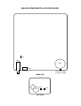
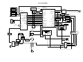
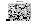
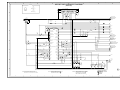
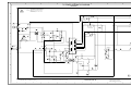
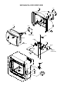
FILE NO. 050-200111
SERVICE MANUAL
COLOR TELEVISION
13A21C
SERVICING NOTICES ON CHECKING
1. KEEP THE NOTICES
6. AVOID AN X-RAY
As for the places which need special attentions,
they are indicated with the labels or seals on the
cabinet, chassis and parts. Make sure to keep the
indications and notices in the operation manual.
2. AVOID AN ELECTRIC SHOCK
There is a high voltage part inside. Avoid an
electric shock while the electric current is
flowing.
Safety is secured against an X-ray by considering about the cathode-ray tube and the high
voltage peripheral circuit, etc.
Therefore, when repairing the high voltage peripheral circuit, use the designated parts and
make sure not modify the circuit.
Repairing except indicates causes rising of high
voltage, and it emits an X-ray from the cathoderay tube.
3. USE THE DESIGNATED PARTS
The parts in this equipment have the specific
characters of incombustibility and withstand
voltage for safety. Therefore, the part which is
replaced should be used the part which has
the same character.
Especially as to the important parts for safety
which is indicated in the circuit diagram or the
table of parts as a
mark, the designated
parts must be used.
4. PUT PARTS AND WIRES IN THE
ORIGINAL POSITION AFTER
ASSEMBLING OR WIRING
7. PERFORM A SAFETY CHECK AFTER
SERVICING
Confirm that the screws, parts and wiring which
were removed in order to service are put in the
original positions, or whether there are the
portions which are deteriorated around the
serviced places serviced or not. Check the
insulation between the antenna terminal or
external metal and the AC cord plug blades.
And be sure the safety of that.
(INSULATION CHECK PROCEDURE)
There are parts which use the insulation
material such as a tube or tape for safety, or
which are assembled in the condition that
these do not contact with the printed board.
The inside wiring is designed not to get closer
to the pyrogenic parts and high voltage parts.
Therefore, put these parts in the original
positions.
5. TAKE CARE TO DEAL WITH THE
CATHODE-RAY TUBE
1. Unplug the plug from the AC outlet.
2. Remove the antenna terminal on TV and turn
on the TV.
3. Insulation resistance between the cord plug
terminals and the eternal exposure metal
[Note 2] should be more than 1M ohm by
using the 500V insulation resistance meter
[Note 1].
4. If the insulation resistance is less than 1M
ohm, the inspection repair should be
required.
[Note 1]
In the condition that an explosion-proof cathoderay tube is set in this equipment, safety is
secured against implosion. However, when
removing it or serving from backward, it is
dangerous to give a shock. Take enough care to
deal with it.
If you have not the 500V insulation
resistance meter, use a Tester.
[Note 2]
External exposure metal: Antenna terminal
Earphone Jack
HOW TO ORDER PARTS
Please include the following informations when you order parts. (Particularly the VERSION LETTER.)
1. MODEL NUMBER and VERSION LETTER
The MODEL NUMBER can be found on the back of each product and the VERSION LETTER can be
found at the end of the SERIAL NUMBER.
2. PART NO. and DESCRIPTION
You can find it in your SERVICE MANUAL.
IMPORTANT
Inferior silicon grease can damage IC's and transistors.
When replacing an IC's or transistors, use only specified silicon grease (YG6260M).
Remove all old silicon before applying new silicon.
GENERAL SPECIFICATIONS
G-1
TV
System
CRT
CRT Size / Visual Size
CRT Type
Deflection
Magnetic Field
BV/BH
Color System
Speaker
Position
Size
Impedance
MAX
10%(Typical)
Sound Output
G-2
Tuning
System
NTSC3.58+4.43 /PAL60Hz
Broadcasting System
Tuner and
Receive CH
CH Coverage
Picture(FP)
Sound(FS)
FP-FS
Intermediate
Frequency
G-3
Power
Preset CH
Stereo/Dual TV Sound
Tuner Sound Muting
Power Source
Power Consumption
Regulation
G-5
Temperature
G-6
G-7
Operating Humidity
On Screen
Menu
Display
AC
DC
at AC
Stand by (at AC)
Per Year
Power Fuse
Safety
Radiation
X-Radiation
Operation
Storage
Protector
G-4
System
Destination
Tuning System
Input Impedance
Menu Type
Picture
Contrast
Brightness
Color
Tint
Sharpness
Audio
Bass
Treble
Balance
BBE On/Off
Stable Sound On/Off
CH Set Up
TV/CABLE(CATV)
Auto CH Memory
Add/ Delete
Language
V-chip
CH Label
Favorite CH
Color Stream DVD/DTV
Control Level
Volume
Brightness
Contrast
Color
Tint (NTSC Only)
Sharpness
Tuning
Bass
Treble
Balance
Back Light
Stereo,Audio Output,SAP
Video
Color Stream
Channel(TV/Cable)
CH Label
Sleep Timer
Sound Mute
V-chip Rating
13 inch / 335.4mmV
Normal
90 degree
+0.45G/0.18G
NTSC
1Speaker
Bottom
3 Inch
8
ohm
1.0
W
0.8
W
No
US System M
1Tuner
Ohers
F-Synth
VHF/UHF 75 ohm
2 - 69, 4A, A-5 - A-1,
A - I, J - W, W+1 - W+84
45.75MHz
41.25MHz
4.50MHz
No
No
Yes
120V AC 60Hz
54 W at AC 120 V 60 Hz
5 W at AC 120 V 60 Hz
-kWh/Year
Yes
CSA
DOC
HWC
+5oC ~ +40oC
-20oC ~ +60oC
Less then 80% RH
Yes
Character
Yes
Yes
Yes
Yes
Yes
Yes
No
No
No
No
No
No
Yes
Yes
Yes
Yes
Yes
No
No
No
No
Yes
Yes
Yes
Yes
Yes
Yes
Yes
No
No
No
No
No
No
Yes
No
Yes
No
Yes
Yes
No
GENERAL SPECIFICATIONS
G-8
G-9
G-10
OSD Language
Clock and
Timer
Remote
Control
Sleep Timer
OSD Language Setting
Max Time
Step
Program(On Tim / Off Tim)
On/Off Timer
Wake Up Timer
Timer Back-up (at Power Off Mode)
more than
Unit
Glow in Dark Remocon
Format
Custom Code
Power Source
Voltage(D.C)
UM size x pcs
Total Keys
Keys
Power
1
2
3
4
5
6
7
8
9
0
100
Multi Brand Keys
CH Up
CH Down
Volume Up
Volume Down
TV/Caption/Text
CH1/CH2
TV/Video(TV/AV)
CH RTN/CH ENT(Quick View)
Sleep
RE Call(Call)
Reset
Menu
Enter
Mute
Exit
MTS(Audio Select)
Set +
Set CH Up(VCR)
CH Down(VCR)
Pause/Still
TV/VCR(VCR)
Code
FF
Rew
Rec
Play
Stop
TV
VCR
Cable
English French
English
120 Min
10 Min
No
No
-Min
RC-EH
No
Toshiba
40-BF h
3V
UM-4 x 2 pcs
27
Keys
Yes
Yes
Yes
Yes
Yes
Yes
Yes
Yes
Yes
Yes
Yes
No
Yes
Yes
Yes
Yes
Yes
Yes
Yes
Yes
Yes
Yes
Yes
Yes
Yes
Yes
No
No
Yes
Yes
No
No
No
No
No
No
No
No
No
No
No
No
No
Spanish
Sec
GENERAL SPECIFICATIONS
G-11
Features
Auto Degauss
Auto Shut Off
Canal+
CATV
Anti-theft
Rental
Memory(Last CH)
Memory(Last Volume)
V-Chip
Yes
Yes
No
Yes
No
No
Yes
Yes
Type
BBE
Auto Search
CH Allocation
SAP
Channel Lock
Just Clock Function
Game Position
CH Label
VM Circuit
Full OSD
Premiere
Comb Filter
G-12
Accessories
Auto CH Memory
Hotel Lock
Closed Caption
Stable Sound
FBT Leak Test Protect
Favorite CH
Owner's Manual
Language
W/ Warranty
Remote Control Unit
Rod Antenna
Poles
Terminal
No
USA,ORION Type
No
No
No
No
No
No
No
No
No
No
No
No
Lines
Yes
No
Yes
No
Yes
No
English/French
No
Yes
No
Loop Antenna
Terminal
U/V Mixer
DC Car Cord (Center+)
Guarantee Card
Warning Sheet
Circuit Diagram
Antenna Change Plug
Service Station List
Important Safety Instruction
Dew/AHC Caution Sheet
AC Plug Adapter
Quick Set-up Sheet
Battery
-
Yes
Yes
UM size x pcs
OEM Brand
AC Cord
AV Cord (2Pin-1Pin)
Registration Card (NDL Card)
ESP Card
PTB Sheet
300 ohm to 75 ohm Antenna Adapter
Envelop
Yes
UM4 x 2
Yes
No
No
No
No
No
No
No
No
No
No
No
No
No
No
No
No
Yes
GENERAL SPECIFICATIONS
G-13
Interface
Switch
Front
Rear
Indicator
Terminals
Front
Rear
G-14
G-15
Set Size
Weight
G-16
Carton
Power
System Select
Main Power SW
Sub Power
Channel Up/Reset
Channel Down/Enter
Volume Up/Set Up
Volume Down/Set Down
MENU=Volume Up+Volume Down
AC/DC
TV/CATV Selector
Degauss
Main Power SW
Power
Stand-by
On Timer
Video Input
Audio Input
Other Terminal
Video Input(Rear1)
Video Input(Rear2)
Audio Input(Rear1)
Audio Input(Rear2)
Video Output
Audio Output
Euro Scart
Color Stream
Diversity
Ext Speaker
DC Jack 12V(Center +)
VHF/UHF Antenna Input
AC Outlet
Approx.
W x D x H (mm)
Net (Approx.)
Gross (Approx.)
Master Carton
Content
Material
Dimensions
W x D x H(mm)
Description of Origin
Gift Box
Material
Dimensions
W x D x H(mm)
Design
Description of Origin
Drop Test
G-17
Cabinet Material
Height (cm)
Container Stuffing
Cabinet Front
Cabinet Rear
Yes
No
No
No
Yes
Yes
Yes
Yes
Yes
No
No
No
No
Yes
No
No
RCA
RCA x 1
Ear Phone
No
No
No
No
No
No
No
No
No
No
No
F Type
No
362 x 360 x 320.5
9.5 kg
( 20.9 lbs)
11.0kg
( 24.4lbs)
No
---Sets
-/--- x -- x -No
Yes
Double/Brown
440 x 408 x 380
As per Buyer's
Yes
Natural
Dropping
At 1
Corner / 3
Edges / 6
Surfaces
62
866
Sets/40' container
PS 94V0 DECABROM
PS 94V0 DECABROM
DISASSEMBLY INSTRUCTIONS
3. After one side is removed, pull in the opposite direction to
remove the other.
1. REMOVAL OF ANODE CAP
Read the following NOTED items before starting work.
* After turning the power off there might still be a potential
voltage that is very dangerous. When removing the
Anode Cap, make sure to discharge the Anode Cap's
potential voltage.
* Do not use pliers to loosen or tighten the Anode Cap
terminal, this may cause the spring to be damaged.
NOTE
Take care not to damage the Rubber Cap.
INSTALLATION
1. Clean the spot where the cap was located with a small
amount of alcohol. (Refer to Fig. 1-3.)
REMOVAL
1. Follow the steps as follows to discharge the Anode Cap.
(Refer to Fig. 1-1.)
Connect one end of an Alligator Clip to the metal part of a
flat-blade screwdriver and the other end to ground.
While holding the plastic part of the insulated Screwdriver,
touch the support of the Anode with the tip of the
Screwdriver.
A cracking noise will be heard as the voltage is discharged.
Location of Anode Cap
GND on the CRT
Fig. 1-3
NOTE
Confirm that there is no dirt, dust, etc. at the spot where
the cap was located.
2. Arrange the wire of the Anode Cap and make sure the
wire is not twisted.
3. Turn over the Rubber Cap. (Refer to Fig. 1-4.)
CRT
Screwdriver
Support
Alligator Clip
GND on the CRT
Fig. 1-1
2. Flip up the sides of the Rubber Cap in the direction of the
arrow and remove one side of the support.
(Refer to Fig. 1-2.)
Fig. 1-4
4. Insert one end of the Anode Support into the anode button,
then the other as shown in Fig. 1-5.
Rubber Cap
CRT
Support
Fig. 1-2
CRT
Support
Fig. 1-5
5. Confirm that the Support is securely connected.
6. Put on the Rubber Cap without moving any parts.
DISASSEMBLY INSTRUCTIONS
2. REMOVAL AND INSTALLATION OF
FLAT PACKAGE IC
REMOVAL
3. When IC starts moving back and forth easily after
desoldering completely, pickup the corner of the IC using
a tweezers and remove the IC by moving with the IC
desoldering machine. (Refer to Fig. 2-3.)
NOTE
1. Put the Masking Tape (cotton tape) around the Flat
Package IC to protect other parts from any damage.
(Refer to Fig. 2-1.)
Some ICs on the PCB are affixed with glue, so be
careful not to break or damage the foil of each IC
leads or solder lands under the IC when removing it.
NOTE
Masking is carried out on all the parts located within
10 mm distance from IC leads.
Masking Tape
(Cotton Tape)
Blower type IC
desoldering
machine
IC
Tweezers
Fig. 2-1
IC
Fig. 2-3
2. Heat the IC leads using a blower type IC desoldering
machine. (Refer to Fig. 2-2.)
4. Peel off the Masking Tape.
NOTE
Do not add the rotating and the back and forth
directions force on the IC, until IC can move back and
forth easily after desoldering the IC leads completely.
5. Absorb the solder left on the pattern using the Braided
Shield Wire. (Refer to Fig. 2-4.)
NOTE
Do not move the Braided Shield Wire in the vertical
direction towards the IC pattern.
Blower type IC
desoldering machine
Braided Shield Wire
Soldering Iron
IC
Fig. 2-2
IC pattern
Fig. 2-4
DISASSEMBLY INSTRUCTIONS
INSTALLATION
1. Take care of the polarity of new IC and then install the
new IC fitting on the printed circuit pattern. Then solder
each lead on the diagonal positions of IC temporarily.
(Refer to Fig. 2-5.)
4. When bridge-soldering between terminals and/or the
soldering amount are not enough, resolder using a Thintip Soldering Iron. (Refer to Fig. 2-8.)
Thin-tip Soldering Iron
IC
Soldering Iron
Fig. 2-8
Solder temporarily
Solder temporarily
Fig. 2-5
2. Supply the solder from the upper position of IC leads
sliding to the lower position of the IC leads.
(Refer to Fig. 2-6.)
Solder
IC
Soldering Iron
Supply soldering
from upper position
to lower position
Fig. 2-6
3. Absorb the solder left on the lead using the Braided
Shield Wire. (Refer to Fig. 2-7.)
NOTE
Do not absorb the solder to excess.
Soldering Iron
IC
Braided Shield Wire
Fig. 2-7
5. Finally, confirm the soldering status on four sides of the
IC using a magnifying glass.
Confirm that no abnormality is found on the soldering
position and installation position of the parts around the
IC. If some abnormality is found, correct by resoldering.
NOTE
When the IC leads are bent during soldering and/or
repairing, do not repair the bending of leads. If the
bending of leads are repaired, the pattern may be
damaged. So, be always sure to replace the IC in this
case.
SERVICE MODE LIST
This unit provided with the following SERVICE MODES so you can repair, examine and adjust easily.
To enter the Service Mode, press both set key and remote control key for more than 1 second.
Set Key
Remocon Key
VOL. (-) MIN
0
Releasing of V-CHIP PASSWORD.
VOL. (-) MIN
1
Initialization of the factory.
NOTE: Do not use this for the normal servicing.
Operations
POWER ON total hours is displayed on the screen.
Refer to the "CONFIRMATION OF USING HOURS".
VOL. (-) MIN
6
Can be checked of the INITIAL DATA of MEMORY IC.
Refer to the "NOTE FOR THE REPLACING OF MEMORY IC".
VOL. (-) MIN
8
Writing of EEPROM initial data.
NOTE: Do not use this for the normal servicing.
VOL. (-) MIN
9
Display of the Adjustment MENU on the screen.
Refer to the "ELECTRICAL ADJUSTMENT" (On-Screen Display Adjustment).
CONFIRMATION OF USING HOURS
POWER ON total hours can be checked on the screen. Total hours are displayed in 16 system of notation.
ADDRESS
1. Set the VOLUME to minimum.
2. Press both VOL. DOWN button on the set and Channel
button (6) on the remote control for more than 1 second.
3. After the confirmation of using hours, turn off the power.
INIT
00
DATA
Initial setting content of MEMORY IC.
83
0010
CRT ON
POWER ON total hours.
= (16 x 16 x 16 x thousands digit value)
+ (16 x 16 x hundreds digit value)
+ (16 x tens digit value)
+ (ones digit value)
FIG. 1
NOTE FOR THE REPLACING OF MEMORY IC
If a service repair is undertaken where it has been required to change the MEMORY IC, the following steps should be taken to
ensure correct data settings while making reference to TABLE 1.
INI
+0
+1
+2
+3
+4
+5
+6
+7
+8
+9
+A
+B
00
88
09
A2
01
06
B3
24
09
28
24
FF
03
Table 1
1. Enter DATA SET mode by setting VOLUME to minimum.
2. Press both VOL. DOWN button on the set and Channel button (6) on the remote control for more than 1 second.
ADDRESS and DATA should appear as FIG 1.
3. ADDRESS is now selected and should "blink". Using the SET + or - keys on the remote, step through the ADDRESS until
required ADDRESS to be changed is reached.
4. Press ENTER to select DATA. When DATA is selected, it will "blink".
5. Again, step through the DATA using SET + or - until required DATA value has been selected.
6. Pressing ENTER will take you back to ADDRESS for further selection if necessary.
7. Repeat steps 3 to 6 until all data has been checked.
8. When satisfied correct DATA has been entered, turn POWER off (return to STANDBY MODE) to finish DATA input.
The unit will now have the correct DATA for the new MEMORY IC.
ELECTRICAL ADJUSTMENTS
1. BEFORE MAKING ELECTRICAL
ADJUSTMENTS
2. BASIC ADJUSTMENTS
Read and perform these adjustments when repairing the
circuits or replacing electrical parts or PCB assemblies.
1.
2.
3.
4.
2-1: RF AGC DELAY
CAUTION
• Use an isolation transformer when performing any
service on this chassis.
• Before removing the anode cap, discharge electricity
because it contains high voltage.
• When removing a PCB or related component, after
unfastening or changing a wire, be sure to put the wire
back in its original position.
Inferior silicon grease can damage IC's and transistors.
• When replacing IC's and transistors, use only specified
silicon grease.
Remove all old silicon before applying new silicon.
Prepare the following measurement tools for electrical
adjustments.
1. Oscilloscope
2. Digital Voltmeter
2-2: CUT OFF
1. Adjust the unit to the following settings.
R.DRIVE=10, B.DRIVE=10, R.BIAS=64, G.BIAS=64,
B.BIAS=64, BRIGHTNESS=100, CONTRAST=64.
2. Place the set with Aging Test for more than 15 minutes.
3. Activate the adjustment mode display of Fig. 1-1 and
press the channel button (01) on the remote control to
select "CUT OFF".
4. Adjust the Screen Volume until a dim raster is obtained.
2-3: FOCUS
On-Screen Display Adjustment
1. In the condition of NO indication on the screen.
Press the VOL. DOWN button on the set and the
Channel button (9) on the remote control for more than
1 second to appear the adjustment mode on the screen
as shown in Fig. 1-1.
TV
00 OSD
15
Fig. 1-1
2. Use the Channel UP/DOWN button or Channel button
(0-9) on the remote control to select the options shown
in Fig. 1-2.
3. Press the MENU button on the remote control to end
the adjustments.
NO.
00
01
02
03
04
05
06
07
08
09
10
11
12
Place the set with Aging Test for more than 15 minutes.
Receive a 63dB monoscope pattern.
Connect the digital voltmeter to R606.
Activate the adjustment mode display of Fig. 1-1 and
press the channel button (02) on the remote control to
select "RF AGC DELAY".
5. Press the VOL. UP/DOWN button on the remote control
until the digital voltmeter is 2.5 ± 0.05V.
FUNCTION
OSD H
CUT OFF
RF AGC DELAY
VIF VCO
H VCO
H PHASE
V SIZE
V SHIFT
R DRIVE
B DRIVE
R BIAS
G BIAS
B BIAS
NO.
13
14
15
16
17
18
19
20
21
22
23
24
FUNCTION
BRIGHTNESS
CONTRAST
COLOR
TINT
SHARPNESS
FM LEVEL
LEVEL
SEPARATION 1
SEPARATION 2
TEST MONO
TEST STEREO
X-RAY TEST
Fig. 1-2
1. Receive the monoscope pattern.
2. Turn the Focus Volume fully counterclockwise once.
3. Adjust the Focus Volume until picture is distinct.
2-4: WHITE BALANCE
NOTE: Adjust after performing CUT OFF adjustment.
1. Place the set with Aging Test for more than 10 minutes.
2. Receive the white 100% signal from the Pattern
Generator.
3. Using the adjustment control, set the brightness and
contrast to normal position.
4. Activate the adjustment mode display of Fig. 1-1 and
press the channel button (10) on the remote control to
select "R.BIAS".
5. Using the VOL. UP/DOWN button on the remote control,
adjust the R.BIAS.
6. Press the CH. UP/DOWN button on the remote control to
select the "R.DRIVE", "B.DRIVE", "G.BIAS" or "B.BIAS".
7. Using the VOL. UP/DOWN button on the remote control,
adjust the R.DRIVE, B.DRIVE, G.BIAS or B.BIAS.
8. Perform the above adjustments 6 and 7 until the white
color is looked like a white.
2-5: SUB TINT/SUB COLOR
1. Receive the color bar pattern. (RF Input)
2. Connect the oscilloscope to TP023.
3. Activate the adjustment mode display of Fig. 1-1 and
press the channel button (16) on the remote control to
select "TINT".
4. Press the VOL. UP/DOWN button on the remote control
until the section "A" becomes a straight line.
(Refer to Fig. 2-1)
5. Connect the oscilloscope to TP022.
6. Press the CH DOWN button once to set to "COLOR"
mode.
7. Press the VOL. UP/DOWN button on the remote control
until the red color level is adjusted to 110% of the white
level. (Refer to Fig. 2-2)
8. Receive the color bar pattern. (Audio Video Input)
9. Press the TV/VIDEO button on the remote control to set to
the AV mode. Then perform the above adjustments 2~7.
ELECTRICAL ADJUSTMENTS
2-9: OSD HORIZONTAL
1. Activate the adjustment mode display of Fig. 1-1.
2. Press the VOL. UP/DOWN button on the remote
control until the difference of A and B becomes
minimum. (Refer to Fig. 2-3)
"A"
Fig. 2-1
TV
0%
00 OSD
15
110%
A
100%
Fig. 2-2
2-6: HORIZONTAL PHASE
1. Receive the center cross signal from the Pattern
Generator.
2. Activate the adjustment mode display of Fig. 1-1 and
press the channel button (05) on the remote control to
select "H PHASE".
3. Press the VOL. UP/DOWN button on the remote
control until the SHIFT quantity of the OVER SCAN on
right and left becomes minimum.
2-7: VERTICAL SIZE
NOTE: Adjust after performing adjustments in section 2-6
1. Receive the crosshatch signal from the Pattern
Generator.
2. Activate the adjustment mode display of Fig. 1-1 and
press the channel button (06) on the remote control to
select "V SIZE".
3. Press the VOL. UP/DOWN button on the remote control
until the rectangle on the center of the screen becomes
square.
4. Receive a broadcast and check if the picture is normal.
2-8: VERTICAL SHIFT
NOTE: Adjust after performing adjustments in section 2-7
1. Receive the crosshatch signal from the Pattern
Generator.
2. Activate the adjustment mode display of Fig. 1-1 and
press the channel button (07) on the remote control to
select "V SHIFT".
3. Press the VOL. UP/DOWN button on the remote
control until the horizontal line becomes fit to the notch
of the shadow mask.
B
Fig. 2-3
2-10: VIF VCO
1. Place the set with Aging Test for more than 10 minutes.
2. Receive an 80dB monoscope pattern.
3. Connect the digital voltmeter between the pin 5 of
CP601 and the GND.
4. Activate the adjustment mode display of Fig. 1-1 and
press the channel button (03) on the remote control to
select "VIF VCO".
5. Press the VOL. UP/DOWN button on the remote control
until the digital voltmeter is 2.5V.
2-11: SUB CONTRAST NORMAL
1. Activate the adjustment mode display of Fig. 1-1
press the channel button (14) on the remote control to
select "CONTRAST".
2. Press the VOL. UP/DOWN button on the remote control
until the contrast step No. becomes "110".
3. Press the TV/VIDEO button on the remote control
to set to the AV mode. Then perform the above
adjustments 2~3.
2-12: BRIGHTNESS
1. Activate the adjustment mode display of Fig. 1-1 and
press the channel button (13) on the remote control to
select "BRIGHTNESS".
2. Press the VOL. UP/DOWN button on the remote control
until the brightness step No. becomes "96".
3. Press the TV/VIDEO button on the remote control to set
to the AV mode. Then perform the above adjustments
1~2.
4. Press the TV/VIDEO button on the remote control to set
to the CS mode. Then perform the above adjustments
1~2.
ELECTRICAL ADJUSTMENTS
3. PURITY AND CONVERGENCE
ADJUSTMENTS
NOTE
1. Turn the unit on and let it warm up for at least 30
minutes before performing the following adjustments.
2. Place the CRT surface facing east or west to reduce the
terrestrial magnetism.
3. Turn ON the unit and demagnetize with a Degauss Coil.
3-1: STATIC CONVERGENCE (ROUGH ADJUSTMENT)
1. Tighten the screw for the magnet. Refer to the adjusted
CRT for the position. (Refer to Fig. 3-1)
If the deflection yoke and magnet are in one body,
untighten the screw for the body.
2. Receive the green raster pattern from the color bar
generator.
3. Slide the deflection yoke until it touches the funnel
side of the CRT.
4. Adjust center of screen to green, with red and blue on the
sides, using the pair of purity magnets.
5. Switch the color bar generator from the green raster
pattern to the crosshatch pattern.
6. Combine red and blue of the 3 color crosshatch pattern
on the center of the screen by adjusting the pair of
4 pole magnets.
7. Combine red/blue (magenta) and green by adjusting the
pair of 6 pole magnets.
8. Adjust the crosshatch pattern to change to white
by repeating steps 6 and 7.
3-2: PURITY
3-3: STATIC CONVERGENCE
NOTE
Adjust after performing adjustments in section 3-2.
1. Receive the crosshatch pattern from the color bar
generator.
2. Combine red and blue of the 3 color crosshatch pattern
on the center of the screen by adjusting the pair of
4 pole magnets.
3. Combine red/blue (magenta) and green by adjusting the
pair of 6 pole magnets.
3-4: DYNAMIC CONVERGENCE
NOTE
Adjust after performing adjustments in section 3-3.
1. Adjust the differences around the screen by moving
the deflection yoke upward/downward and right/left.
(Refer to Fig. 3-2-a)
2. Insert three wedges between the deflection yoke and
CRT funnel to fix the deflection yoke.
(Refer to Fig. 3-2-b)
RGB
R
G
B
RGB
R
G
B
UPWARD/DOWNWARD SLANT
NOTE
Fig. 3-2-a
Adjust after performing adjustments in section 3-1.
1. Receive the green raster pattern from color bar
generator.
2. Adjust the pair of purity magnets to center the
color on the screen.
Adjust the pair of purity magnets so the color at the
ends are equally wide.
3. Move the deflection yoke backward (to neck side)
slowly, and stop it at the position when the whole
screen is green.
4. Confirm red and blue colors.
5. Adjust the slant of the deflection yoke while watching the
screen, then tighten the fixing screw.
DEFLECTION YOKE
DEFLECTION YOKE SCREW
MAGNET SCREW
PURITY MAGNETS
6 POLE MAGNETS
4 POLE MAGNETS
Fig. 3-1
RIGHT/LEFT SLANT
WEDGE
WEDGE
WEDGE
WEDGE POSITION
Fig. 3-2-b
MAJOR COMPONENTS LOCATION GUIDE
R606
TU001
FB401
CP601
FOCUS VOLUME
SCREEN VOLUME
MAIN PCB
TP023
TP022
J801
CRT PCB
BLOCK DIAGRAM
SDA
SCL
AGC
VOL UP
IF
TU001
CH UP
11
5
4
1
X602
3.579545MHz
CHROMA IC
IC601 M61206FP
IC351 AN7511
32 X' TAL
AUDIO OUT 50
MICON IC
IC101 OEC7063A
CH DOWN
CF601
SAW FILTER
VOL DOWN
5
P02/AUDIO MUTE
26 AD6/KEY2
POWER
GREEN G 41
28 G IN
G OUT 15
BLUE B 40
20 B IN
B OUT 16
X101
EFOEC8004T4
27 FAST BLK
5.7V REG OUT 41
1
12 INV FBP OUT
P51/V. SYNC
2
29 V PULSE OUT
SCL1 34
5 SCL
SDA1 32
10 SDA
RESET 25
FBP IN
GREEN OUT
Q603
Q803
REG
5
6
MEMORY IC
SDA SCL IC199
S-24C02BDP-1A
6
H OUT
7
Q604, Q605
5V REG 39
52 EXT AUDIO IN
VREG VCC 55
34 EXT C IN
V OUT 17
REG
Q402
H. DRIVE
Q401
29 X-RAY
H. OUTPUT
V-OUT IC
IC401 AN5522
J703
1
Q504
PROTECT
DRIVE
Q802
START UP VCC 19
42 MCU RESET
20 XOUT
Q503
RED OUT
BLUE OUT
P50/H. SYNC
19 XIN
UNREG + 12V
Q801
R OUT 14
3
SP351
REG
8.7V REG OUT 33
30 R IN
AT+5V
2
SW
Q606
VIF IN (2)
27 AD5/KEY1 RED R 42
OUT1/BLANK BL 39
10 INT1/REMOCON
1
6
SOUND AMP
IC
4
8
40 Y SW OUT
CVIN 17
OS101
POWER ON 13
CONT
64 VIF IN (1)
1
2
Q607
62 RF AGC OUT
PUMP UP
2
AMP
+
J702
FEED BACK
1
2
5
6
BUFFER
SW
Q507
FEED BACK
SW.
T502
13
DEGAUSS COIL
L503
D501~D504
DY
RECTIFIER
FB401
8
9
6
L501
3
16
5
1
F
1
2
S
2
10
HV
13
3
UNREG + 12V
F501
AC IN
7
G
R
F
8
4
2
Q502
Q501
9
B
Heater
VCC
7
3
CRT
J352
S501B
C505_1
TH501
TP002
D109
R511
W821
S501A
D501
Q802
W067
L801_1
R505
R356
D502
D507
D503
R806
R508
C509
CP806
SW105
C819_1
R501
Q501
D405
R805_1
D410
SW104
R804
C506
C508
R432
C448
W803
SW103
R803_1
D510
2
1_
52
C
C530
L405
SW102
C351
R701
W040
SW101
C702
C355
C642
C647
R623
W827
W078
W103
W053
CD351
R613_1
R408
R520
1
R517_
C519_1
R807_1
C516
C435
C424
C437
C403
C515
W046
J702
W062
L101
W815
W809
W813
C115
C118
W060
J703
C613
W016
W004
W102
W002
W003
C128_1
W061
W005
W015
D612
W042
W012
W013
L606
CF604
C623
C003
C121
C122
D615
D616
C124
AGC
C601
C002
D001
C004
W837
W817
C639
R618
C602_1
C634
R624
C603
W818
W105
W081
D613
C130
W001
C621_1
D610
W011
W051
W010
W806
D602
D402
D401
D601
W097
C125
C119
C636
W017
W057
C129
C612
W014
R641
R401
R001
W054
C625
C635
C627
W112
W810
C137
C638
C439
W100
CP601
R415
HS401
R407
R426
D403
R421
01
CP4
IC401
C414
D408
R445
R515
D605
W816
C645
W072
W079
D516
D519
D514
T401
R427
R524
C434
C417_1
R703
W058
W820
C427_1
TU001
W049
R115
C607
IC351
W104
R110
W099
W018
C624
C637
CF601
L601
C606
C632
C604
X602
C352
C354
W835
Q603
Q801
OS101
D504
X101_1
D611
W027
CF603
C609
R002
W031
W032
W029
W028
R405
W007
W052
D406
C605
R410
L607
W076
R606
Q606
W044
W008
R645
R404
C134
R446
W101
W047
C446_1
W819
Q605
Q507
C622
R418_1
IC199
C440
C356
R518
W110
W069
Q402
R413
R525
C630
R417_1
Q607
R514
R523
Q604
W045
R414
W023
W070
W111
W019
W833
W025
A
01
Q504
C407
R423
D505
W822
W098
W107
HS402
R416
D518
C517
802
W050
R507
C418
C443
D411
Q503
Q401
R409
C422
B504
D513
T502
CP
W024
Q803
D506
C520
R802
TP003
R403
D404
01X
W074
C406
S1
R510
HS501
C501
TP024
D508
D512
W026
Q502
J8
D528
C442_1
W106
C502
C801
C503
R542
CP801
_1
CP802B
W804
4A125VOR250V
FH501
FH502
C526_1
S101Y
W068
14
C5
TP004
04
_A_V
L501_1
TP022
TP023
29
R4
C511
FB401
CP502
F501
R5
R500_1
D509
R6
29
PRINTED CIRCUIT BOARDS
MAIN/CRT (INSERTED PARTS)
SOLDER SIDE
CD501_2
.
R509
R513
R111
R360
R813
C353
33
R632
C655
R611
R634
R602
R639
49
C626
R609
R512
R620
R617
R615
R622
C618
R131
R114
R129
R627 R630
R631
R625
R619
R614
R601
C650
R419
R122
R635
R124
R104
IC601
R519
R007
R642
R646
C616
R102
R103
17
1
R633
R120
R116
R130
R626
R406
R702
R628
R638
R127
R123 R121
C117
R006
R107 R105
R106
C113
IC101
R353
R132
R113
R119
R117
C114
C140
R357
R128
R134
C120
C138
R506
R359
R354
R101
R126
C116
C805_1
C804_1
R811
R809
R815
C806_1
R814
R816
R112
PRINTED CIRCUIT BOARDS
MAIN/CRT (CHIP MOUNTED PARTS)
SOLDER SIDE
R605
R420
A
B
C
D
E
F
G
H
MICON/TUNER SCHEMATIC DIAGRAM
ACCESSORY
(MAIN PCB)
8
8
UM-4
BT001
R03(AB)E_20_T
13
4.6
1.3
NC
6.2
NC
4.8
NC
4.8
4.9
0
NC
12
2
1 AGC
3 ADRES
4 SCL
5 SDA
6 V.S
10
30.0
0
0
NC
14
8
15
11 IF
7 BPL
TECC1040PG32D
9 BTL
TU001
UM-4
BT002
R03(AB)E_20_T
TM101
RC-EH010
470 YK
7
FROM/TO CHROMA
6.3V
C002
HZ30-3L
D001
C004
7
0.022 F
C003
50V 4.7 KA
OS101
PIC-28143SY-2
AGC
GND
3 GND
2 B+
TUNER+5V
POWER LED
D109
0
4.9
4.8
1 Vout
W837
R132
R002
R001
18K 1/2W
18K 1/2W
IF
270
SLR-342VCT32
6
6
I2C_OFF
VD
IC101
HD
MICON IC
OEC7063A
3
C137
4.7K
R120
0
4.7K
39
P20/AV2
38
NC
0
P03/(Surround)
P21/AV1
37
NC
0
P04
P22/POWER
36
34
32
NC
0
31
0
4.7K
W809
AFT
W813
R112
4.9
26
W815
2.2K
R113
2.2K
50V 0.1
KA
W835
AT+5V
Y_VIDEO
2.7K
SW101
SKHVBED010
1
0
560
2
560
SW102
SKHVBED010
CH UP
2
0
R126
CH DOWN
3
0
R101
SW103
SKHVBED010
E2
VSS
4
R128
VOL UP
8
SW104
SKHVBED010
7
VOL DOWN
SDA
6
470 YK
0
SYNC
4.9
SW105
SKHVBED010
0
POWER
4.8
MEMORY IC
IC199
S-24C02BDP-1A
4.8
5
C118
6.3V
C119
C128_1
6.3V 100 YK
22
W820
4.9
2
0.1 F
23
12P CH
2.5
0
W819
F
VCC
1.6
RESET
1K
12P CH
C113
2.7K
VSS
2.5
L101
OSC2
3.3uH
R127
Xout
24
OSC1
C114
C115
2.5
Xin
3
R119
0.1
RESET
25
18
CNVSS
SDA
0
2.3
2
SCL
10K
4.8
0
3
X101_1
EFOEC8004T4
AD6/KEY2
2.6
19
1
680
POWER
R107
VCC
AD5/KEY1
FROM/TO CHROMA
4.7K
E0
17
CVIN
220P B
R106
C134
16
V.HOLD
NC
3.2
SCL
AD4/AFT
X-RAY
C116
MODE
15
HLF
4
4.7K
270
E1
X-RAY
+B
R105
R007
4.8
30
AVCC
220P B
29
P25/ON_TIMER AD1/X_RAY_TEST
20
Y
C138
470
560P W
2
1M
F
1
0.01
SDA2
C117
270
FROM DEFLECTION/CRT
NC
3.2
R134
R129
0.1
P24
0.2
0.001 Y
C130
SDA1
1.9
C120
C124
3
P23/SYNC
4.9
1K
CH
R124
POWER
R006
4.8
28
R130
680
AUDIO_MUTE
NC
27
NC
0
200P
33
9
10
11
NC
0
12
100P SL
C121
SCL2
13
0.8
50V 1 KA
INT1/REMOCON
14
C140
C122
SCL1
4.8
W822
47K
INT2/P.FAIL
21
4
R104
TO SOUND/AV
0
4.0
R131
5
FROM TV POWER
X-RAY
R114
100
680
OSD_BLK
35
8
P05/(Center_SP) P10/DEGAUSS_H
0
R115
KA
4.9
0
10K
50V 0.1
50V 0.1 KA
R103
4
5
P02/AUDIO MUTE
0
0
C125
OSD_B
6
10K
0
OSD_G
OUT1/BLANK BL
P01/I2C_OFF
4.8
47K
4.7K
R121
R102
BLUE B
0
50V 0.1 KA
C129
40
3
P00/EXT MUTE
4.7K
R122
41
2
GREEN G
OSD_R
0
7
R110
R111
P51/V.SYNC
0
R117
47K
5
RED R
4.0
4.7
1K 1/4W
R116
P50/H.SYNC
42
1
R123
4
PCB010
TMA511
1
CAUTION: SINCE THESE PARTS MARKED BY
CRITICAL FOR SAFETY,USE ONES
DESCRIBED IN PARTS LIST ONLY
NOTE: THE DC VOLTAGE AT EACH PART WAS MEASURED
WITH THE DIGITAL TESTER WHEN THE COLOR BROADCAST
WAS RECEIVED IN GOOD CONDITION AND PICTURE IS NORMAL.
A
B
C
ARE
D
DEFLECTION SIGNAL
TUNER VIDEO SIGNAL
R.SIGNAL
G.SIGNAL
B.SIGNAL
ATTENTION: LES PIECES REPAREES PAR UN
ETANT
DANGEREUSES AN POINT DE VUE SECURITE
N’UTILISER QUE CELLS DECRITES
DANS LA NOMENCLATURE DES PIECES
E
F
G
1
H
A
B
C
D
E
F
G
H
CHROMA SCHEMATIC DIAGRAM
(MAIN PCB)
8
8
FROM TV POWER
R629
33 3W
UNREG+12V
6
REG
Q604
KTC3203_Y
4.9
R623
120 1/4W
7
7
REG
Q605
KTC3203_Y
7.2
4.9
REG
Q606
KTC3203_Y
7.2
5.5
5.5
M
C622
8.2K
R633
0.015
C625
50V 1 KA
NA
C627
50V 1
C630
100
FROM SOUND/AV
C616
15P CH
100
R628
C636
L606
2.2uH
470
8.5
C647
R615
CF603
EFCT4R5YS5A
16V 47 YK
W816
100
16V 47 YK
R635
C635
C650
4.9
100P SL
R622 L607
5.5
7
11.3
R639
0.01 Y
REG
Q603
KTC3203_Y
CF604
TPSRA4M50C00-A0
68
8.8
15uH
7.9
VIDEO_IN
R638
50V 1
KA
22K
6
6
X602
31
30
29
28
27
W810
25
24
23
22
21
20
19
POWER ON CONT
9
18
10
W818
V_OUT
10V 1000 YK
17
G OUT
R OUT
FROM/TO DEFLECTION/CRT
7.9
V OUT
3.6
10
11
12
13
14
15
16
4.9
3.4 3.9 4.9
2.0 2.0
2.0
11
2.2K
7.9
ABCL
V_FEEDBACK
GND
13
0
STRAT UP Vcc
12
9
0
INV FBP OUT
8
0
AFC FILTER
H OUT
DEF
7
0
SDA
FBP IN
6
4.9
MTZJ12B
R627
100
R630
100
R631
100
R617
1K
1SS133
1SS133
D616
D613
1SS133
D615
12
CLAMP
SWITCHING
Q607
DTC114ESTP
0
R620
D612
MTZJ12B
2.2K
2.2K
R625
R619
R614
G.OUT
R.OUT
GND
TEST POINT
CP601
R613_1
4.9
2
HD
POWER
OSD_B
OSD_BLK
OSD_G
VD
OSD_R
I2C_OFF
SDA
SCL
560 1/2W
0
CAUTION: DIGITAL TRANSISTOR
NOTE: THIS SCHEMATIC DIAGRAM IS THE LATEST AT THE TIME
OF PRINTING AND SUBJECT TO CHANGE WITHOUT NOTICE
1
A
B
NOTE: THE DC VOLTAGE AT EACH PART WAS MEASURED
WITH THE DIGITAL TESTER WHEN THE COLOR BROADCAST
WAS RECEIVED IN GOOD CONDITION AND PICTURE IS NORMAL.
C
CAUTION: SINCE THESE PARTS MARKED BY
CRITICAL FOR SAFETY,USE ONES
DESCRIBED IN PARTS LIST ONLY
D
3
B.OUT
D611
2.2K
MTZJ12B
0.01 Y
C607
D610
C603
50V 1 KA
H_OUT
H_SYNC
8
4.7K
0.01 Y
1000 YK
C637
6.3V
C601
5
R605
F
0
470
C609
3
4
R601
3
4.9
R602
2
4.9
4
0
22K
C634
L601
1.2uH
B IN
R626
1
1.5
IF
H VCO F/B
1.5
SCL
63
RF AGC FILTER
22K +-1%
2.8
17 V OUT
16 B OUT
RF AGC OUT
2.9
0.1
3.579545MHz
32
CHROMA APC FILTER
TV/Y IN
VIDEO/CHROMA GND
5v REG
59
V RAMP FEEDBACK
64 VIF IN (1)
1 VIF IN (2)
C639
AGC
QIF IN
0.01 Y
AFT
AFT OUT
1.9
2K
RESET
C613
50V 1 YK
R641
4.7
R624
TUNER+5V
16V 47 YK
4.9
4.6
SAW FILTER
CF601
SAFGP45M7VHCZR
IN IN G OUTOUT
1 2 3 4 5
NC
7.0
NC
2.8
4.9
VIDEO CHROMA Vcc
V RAMP CAP
64
50V 0.22 KA
CHROMA IC
IC601
M61206FP
2.8
C606
SYNC
57
C618
22P SL
0.01 F
5
C645
0
fsc OUT
VIF Vcc
AT+5V
0.001 Y
11E1-EIC
0
FAST BLK
0
62
R606
55
50V 0.47 KA
R609 C605
C626
C602_1
10K
VIF GND
D605
22K
4.7
G IN
0
0.01 Y
FROM/TO MICON/TUNER
VIF VIDEO OUT
R642
0
SPOT KILLER
2.2
W817
Y_VIDEO
R IN
C638
50V 4.7 KA
2.6
34 EXT C in
33 8.7V REG OUT
32 X’TAL
3.2
470
C624
D601
1SS133
C621_1
4
VREG Vcc
VIF APC FILTER
68K
3.3
ACL/ABCL
8.7
16V 47 YK
D602
MTZJ8.2B
220
VIF VCO F/B
3.2
2.5 3.2 1.9
8.5
36
35
34
33
V PULSE OUT
46 SW REG CONT
47 LIMITER IN
48 IF AGC
49 QIF OUT
2.9
50V 2.2 KA
10M 1/4W
R632
0
37
26
M
58
R618
FM DIRECT OUT
3.0
5.6 0
39
38
C612
C632
5
51
0.0033
52
C623
EXT AUDIO IN
2.2
KA
56
GND
AUDIO BYPASS
53
50V 1
C655
0.0068 Y
KA
60
1
61
W827
2.4
54
C642
50V
AUDIO OUT
Y SW OUT
50
2.3
C604
AUDIO_IN
MCU RESET
10K
5.7 0
41
40
5.7V REG OUT(FOR CPU)
10K
W806
AUDIO_OUT
0.01 Y
R611
5
49
FROM/TO SOUND/AV
0
42
Hi Vcc
R634
7.9 7.9 0
45
44
43
INTELLIGENT MONI
R646
NC
0
3.0 2.2
48
47
46
ARE
ATTENTION: LES PIECES REPAREES PAR UN
ETANT
DANGEREUSES AN POINT DE VUE SECURITE
N’UTILISER QUE CELLS DECRITES
DANS LA NOMENCLATURE DES PIECES
E
F
G
173979-6
B.OUT
6
INT.MONI
5
IIC_OFF
4
SDA
3
SCL
2
GND
1
2
R.SIGNAL
PCB010
G.SIGNAL
TMA511
B.SIGNAL
AUDIO SIGNAL
LUMINANCE SIGNAL
DEFLECTION SIGNAL
TUNER VIDEO SIGNAL
H
1
A
B
C
D
E
F
G
H
TV POWER SCHEMATIC DIAGRAM
(MAIN PCB)
8
8
CAUTION:
ATTENTION:
4A 125V
FOR CONTINUED PROTECTION AGAINST FIRE HAZARD,
REPLACE ONLY WITH THE SAME TYPE 4A 125V (F501)
FUSE.
POUR UNE PROTECTION CONTINUE LES RISQUES
D’INCEIE N’UTILISER QUE DES FUSIBLE DE MEME
TYPE 4A 125V (F501).
TO SOUND/AV
GND
R517_1
D505
SOUND+B
7
C519_1
C516
1W
7
16V
500V 470P B
1.2
470 YK
SB290S
2.7M 1/2W
+-10%
T502
C521_2
5
81290264
10.0
10
12
0
13
5
14
4
15
C509
2
D512
PROTECT DRIVE
Q503
2SA1624
135.0
0
11.3
NC
17
1SS133
R523
10.5
4
1
2
X-RAY
22K 1/2W
1SS133
135.0
R525
2.2K
R512
1SS133
M
11.5
4
D516
R520
R524
150K 1/2W
1.5 2W
3
0.01
2
1SS133
1SS133
D519
D514
FEED BACK 9.5
SWITCHING
Q507
6.0
KTC3198
5.5
68K1/2W
FEED BACK
Q504
LTV-817M-VB
9.5
5.6K
0.1
R513
MTZJ15B
D506
50V 1 YK
TO MICON/TUNER
R514
47K
D518
R515
1SS133
D508
R509
MTZJ15B
1/4W
R508
2.7K
680
R506
16
0
18 NC
C520
0
HS501
763WSA0005
0.1
3
UNREG+12V
0
C511
2.2K
0.047 M
220 1W
0.015 M
R542
0.68 1W
3
BUFFER
Q502
2SC2120Y
4.8
10.3
TO CHROMA
132.3
5.6K
6
3
R505
NC
MHE
6.6
D507
SWITCHING
Q501
144.0 D
2SK2662
G
4.8
0.1 S
C501
250V 0.01 KH
33
250V 0.01 KH
R504
C508
C514_1
S501B
C506
7
3W
10.3
BLACK
WHITE
NC
2KV 680P YR
TP003
003P-2100
W804
S501A
144.0
11
C530
NC
8
100V 10
1.7
51MS040LCC
FH501
FH502
EYF-52BC
EYF-52BC
4
470 YK
C515
16V
R510
1.2M 1/4W
D513
SB290S
1.2M 1/4W
R511
D509
C526_1
C503
D503
1N4005-EIC
D504
200V 220 YK
C502
500V 0.001 B
6
GND
MTZJ18B
D502
5W
1N4005-EIC
4 3
NC
D501
5
1N4005-EIC
1
500V 0.001 B
F501
51MS040LCC
2
5.6
1N4005-EIC
4A 125V
5
R501
L501_1
1R5A102F20
ZPB45BL3R0A
PHE840
TP002
003P-2100
2KV 0.001 YR
160V 100 YXF
UNREG+12V
C517
TH501
AC120V_60Hz
CD501_2
0R414903
+B
RU2AM-EIC
W821
C505_1
2
D510
BL01RN1-A63
TP004
003P-2100
1
1
2
6
CP502
TV-50P-02-A1
TO DEFLECTION/CRT
B504
275V 0.1
DEGAUSS COIL
L503
8R140030
R500_1
SOUND_GND
2
R519
910 1/4W
R507
R518
2.2K +-1%
MTZJ5.6B
D528
1.2K
PCB010
TMA511
1
1
NOTE: THE DC VOLTAGE AT EACH PART WAS MEASURED
NOTE: THIS SCHEMATIC DIAGRAM IS THE LATEST AT THE TIME
OF PRINTING AND SUBJECT TO CHANGE WITHOUT NOTICE
A
B
WITH THE DIGITAL TESTER WHEN THE COLOR BROADCAST
WAS RECEIVED IN GOOD CONDITION AND PICTURE IS NORMAL.
C
D
CAUTION: SINCE THESE PARTS MARKED BY
CRITICAL FOR SAFETY,USE ONES
DESCRIBED IN PARTS LIST ONLY
E
ATTENTION: LES PIECES REPAREES PAR UN
ETANT
DANGEREUSES AN POINT DE VUE SECURITE
N’UTILISER QUE CELLS DECRITES
DANS LA NOMENCLATURE DES PIECES
ARE
F
G
H
E
GND
2
CLAMP
G.OUT
3
3
G.OUT
R.OUT
4
4
R.OUT
B.OUT
5
5
B.OUT
NC
6
6
NC
HEATER
7
7
HEATER
GND
8
8
GND
NC
9
9
NC
180V
10
10
180V
4.7K
470P B
4
3
NC
TP022
TP024
TP023
2
1
AU02A-EIC
2.7K 1/4W
15K 1W
R806
R804
R807_1
CP401
B05B-DVS
R803_1
C434
22
2.7K 1/4W
C427_1
50V 10 YK
R413
4.7K 1/2W
R813
R410
100V 0.15
TF
C422
R416
1 1/2W
25V 470 YK
330 1/2W
100V 22 YK
21
1 YK
330P B
C801
1/2W
68
1
3213012R
COL
HV
FOCUS
7.0
+B
0
R403
NC
22K 1/4W
25.0
C406
S
B+
GND 0
11
AFC
9
HEA
10 TER
8
4
3
SCREEN
ABL
7
4.3
SCREEN
96.4
6.4
GND
0
E12
GND
8
E25
E8
500V 56P SL
5
0
0
NC
3
0
1
48.0
2
FOCUS
F
VIDEO
F
132.5
HS402
763WSA0004
6
5
132.5
CP806
005P-2100
1
SCREEN
7
2KV 0.001 YR
C442_1
0
6
20
C819_1
GND
0
H.OUTPUT
Q401
2SD2627LS-CBC11
130.0
1.6KV 0.0082 ECWH
0
R427
0.3
FROM TV POWER
H.DRIVE
Q402
2SC1473A-QA
50V 22 YK
27.0
7
4
17
130.0
2.7
5
FB401
C446_1
C440
H_OUT
H_SYNC
500V 0.0022 B
ABCL
95.4
250V
C424
16
V_OUT
250V 0.39 PMS
R432
6
C437
4
C443
V_FEEDBACK
3
NC 2
1
100 1/4W
R446
GND
T401
305Y001
4.7K 1/2W
500V 22P SL
1W
D411
L405
12K +-1%
+B
FROM/TO CHROMA
C418
R407
1K
R406
R408
R409
D402
2.7
TO DY
R429
MTZJ11B
98.4
5 7 1
5
4.7
15
1/2W
R
G
B
4.7mH 0909
X-RAY
9
10
8
6
11
15K +-1%
R426
18K 1/4W 2.7K 1/4W
+-1%
R405
D401
MTZJ27B
R401
100K 1/4W
+-1%
820
2.7
V801
A34AGT13X98(L)
R415
2.2
1/2W
560
HS401
763WSA0004
6
3.3K
50V 10
YK
C417_1 R419
22K 1/4W
10K 1/4W
R417_1
R420
100.6
C804_1
R809
19
470
R423
D403
11E1-EIC
R418_1
C439
1
BLUE OUT
Q803
2SC1473A
3.2
GREEN OUT
Q802
2SC1473A
3.2
15K 1W
18
TO MICON/TUNER
1
R414
100 1/4W
RED OUT
Q801
2SC1473A
3.2
CP801
TBS-X01X-A1
560
CD801_1
R814
3.5
C806_1
7
25.0
R805_1
6
12.0
3
14
5
0
4
C414
35V 100
YK
7
4
2.0
8
3
25.0
9
2
3.5
L801_1
1
NC
180V
R816
+
GND
4.7K
NC
180V
NC
HEATER
470P B
560
GND
B.OUT
C805_1
R811
PUMP
UP
R.OUT
R815
NC
HEATER
8
G.OUT
4.7K
AN5522
CLAMP
2.7K 1/4W
IC401
THERMAL
PROTECTION
3
1
2
6
V-OUT IC
4
1
B.OUT
B.OUT
H
GND
GND
R.OUT
R.OUT
G
CP802B
B2013H02-10P
CLAMP
G.OUT
G.OUT
5
GND
CLAMP
CLAMP
F
CP802A
B2013H02-10P
470P B
560
DEFLECTION/CRT SCHEMATIC DIAGRAM(MAIN PCB)
FROM CHROMA
8
D
15K 1W
R802
C
100uH 0305
B
2KV 0.001 B
A
101.6
R645
C407
56P SL
MTZJ6.2B
D404
99.6
J801
HPS3200-010501
D406
2
W833
D405
2
AU02A-EIC
1SS133
D410
47 1/2W
AU02A-EIC
UNREG+12V
PCB110
TCA366
R404
100 1/2W
A
B
C
D408
ATTENTION: LES PIECES REPAREES PAR UN
ETANT
DANGEREUSES AN POINT DE VUE SECURITE
N’UTILISER QUE CELLS DECRITES
DANS LA NOMENCLATURE DES PIECES
11E1-EIC
220K 1/4W
R421
C435
D
100V 0.1 MHE
200V 22 MHE
PCB010
TMA511
C448
1
35V 470 YK
C403
R445
180K 1/4W
CAUTION: SINCE THESE PARTS MARKED BY
CRITICAL FOR SAFETY,USE ONES
DESCRIBED IN PARTS LIST ONLY
E
NOTE: THE DC VOLTAGE AT EACH PART WAS MEASURED
WITH THE DIGITAL TESTER WHEN THE COLOR BROADCAST
WAS RECEIVED IN GOOD CONDITION AND PICTURE IS NORMAL.
ARE
NOTE: THIS SCHEMATIC DIAGRAM IS THE LATEST AT THE TIME
OF PRINTING AND SUBJECT TO CHANGE WITHOUT NOTICE
F
G
R.SIGNAL
G.SIGNAL
B.SIGNAL
DEFLECTION SIGNAL
H
1
A
B
C
D
E
F
G
H
SOUND/AV SCHEMATIC DIAGRAM
(MAIN PCB)
8
8
TO CHROMA
J703
AV1-09D-4
(FRONT)
E
H
AUDIO 2
AUDIO_IN
2
7
R703
7
A_IN
1
25
820 1/4W
47K
R701
75 1/4W
R702
C702
0.0018 B
V_IN
1
2
E
H
26
VIDEO 2
VIDEO_IN
J702
AV1-09D-3
GND
6
6
HEADPHONE_JACK
J352
HSJ1403-01-010
2
C352
R356
3
1
16V 47
YK
12 1/2W
5
5
CD351
CH122301
SPEAKER
SP OUT L+
1
1
SOUND GND
2
2
24
SP351
S08F21
8 OHM
FROM TV POWER
SOUND_GND
4
4
SOUND+B
3.5
6
0
3.4
7
8
+
FROM MICON/TUNER
4
R359
3
5.1
AUDIO_MUTE
47K
SOUND AMP IC
AN7511
8.2
5
-
2
0
IC351
GND
1
0.3
3.9
C354
3
10V 2200 YK
3
R353
POWER
16V 10 KA
C356
0.0015 Y
C353
1
50V
C351
R354
270K
100K
W803
R357
KA
68K
FROM CHROMA
C355
2
50V 0.1 KA
2
WITH THE DIGITAL TESTER WHEN THE COLOR BROADCAST
WAS RECEIVED IN GOOD CONDITION AND PICTURE IS NORMAL.
A
68K
CAUTION: SINCE THESE PARTS MARKED BY
CRITICAL FOR SAFETY,USE ONES
DESCRIBED IN PARTS LIST ONLY
NOTE: THIS SCHEMATIC DIAGRAM IS THE LATEST AT THE TIME
OF PRINTING AND SUBJECT TO CHANGE WITHOUT NOTICE
NOTE: THE DC VOLTAGE AT EACH PART WAS MEASURED
1
23
R360
AUDIO_OUT
B
C
D
ARE
E
PCB010
TMA511
ATTENTION: LES PIECES REPAREES PAR UN
ETANT
DANGEREUSES AN POINT DE VUE SECURITE
N’UTILISER QUE CELLS DECRITES
DANS LA NOMENCLATURE DES PIECES
F
TUNER VIDEO SIGNAL
AUDIO SIGNAL
G
1
H
WAVEFORMS
MICON/TUNER
1 200mV 200ms/div
6 0.5V 20µs/div
11 1V 20µs/div
2 0.5V 20µs/div
7 500mV 20µs/div
12 1V 20µs/div
3 200mV 20µs/div
8
20V 20µs/div
13 1V 20µs/div
DEFLECTION/CRT
4 200mV 5ms/div
9
200mV 20µs/div
14 0.5V 5ms/div
CHROMA
5 0.5V 2ms/div
10 0.5V 5ms/div
15 20V 20µs/div
NOTE: The following waveforms were measured at the point of the corresponding
balloon number in the schematic diagram.
WAVEFORMS
16 2V 20µs/div
21 50V 20µs/div
17 200V 20µs/div
22 50V 20µs/div
26 500mV 20us/div
SOUND/AV
18 10V 5ms/div
23 0.5V 1ms/div
19 10V 5ms/div
24 1V 1ms/div
20 50V 20µs/div
25 500mV 1ms/div
NOTE: The following waveforms were measured at the point of the corresponding
balloon number in the schematic diagram.
MECHANICAL EXPLODED VIEW
201
110
201
113
201
201
114
J801
109
201
114
102
114
PCB110
(CRT PCB)
108
L503
FB401
202
114
V801
203
TU001
203
111
202
205
107
103
204
112
104
106
SP351
105
101
PCB010
(MAIN PCB)
MECHANICAL REPLACEMENT PARTS LIST
Location No. TSB P/N
Reference No.
Description
101
102
103
104
105
106
107
108
109
AD300815
BZ710009
AD300802
AD300808
AD300801
AD300803
AD300804
BZ710260
AD300805
A3J816A720
741WUA0019
713WPAA038
735WPA0396
701WPJB228
713WPAA039
735WPBA226
899HV3T000
702WPAA136
CABINET,FRONT ASSY
SPRING,EARTH
GLASS,LED
SPEAKER HOLDER
CABINET,FRONT
GUIDE,REMOCON
BUTTON,FRAME
HOLDER,ANODE WIRE
CABINET,BACK
110
111
112
113
114
AD300816
AD300843
AD300132
AD300807
BZ710275
722549A027
800WQ00044
7230006818
726000A016
8121J50B54
SHEET,RATING
FELT SHEET
SHEET,CAUTION
SHEET,CRT SERVICEMAN
SCREW,TAPPING(B0) GW20
5x28
201
202
203
204
205
BZ710035
BZ710019
BZ710239
BZ710030
BZ710031
8117540A64
8109630802
8109I30A04
8110630804
8110630A04
SCREW,TAPPING(B0) TRUSS
SCREW,TAP TITE(B) BRAZIER
SCREW,TAP TITE(B) WH7
SCREW,TAP TITE(P) BRAZIER
SCREW,TAP TITE(P) BRAZIER
4x16
3x8
3x10
3x8
3x10
---------------------
AD300809
AD300810
AD300811
AD300817
AD300436
AD300139
AD300140
AD300502
AD300818
AD300845
792WHAA052
792WHAA053
793WCDA987
A3J816A975
J3I70416
J3I70715
J3I70717
J3I70725
J3J81601
JB5UD500
PACKAGE,TOP
PACKAGE,BOTTOM
GIFT BOX
INSTRUCTION BOOK KIT
IMPORTANT SAFETY INSTRUCTIONS
SERVICE STATION LIST
REGISTRATION CARD
ENVELOPE
INSTRUCTION BOOK
POLY BAG
ELECTRICAL REPLACEMENT PARTS LIST
Location No. USA-TOSHIBA
!
!
!
!
!
!
!
!
!
!
!
!
!
!
!
!
!
!
!
!
!
!
Reference No.
RESISTORS
R401
R405
R406
R407
R408
R409
R426
R429
R500
R501
R504
R505
R509
R515
R517
R518
R519
R524
R542
R629
R803
R805
R807
BZ210013
BZ210023
AD300780
BZ210053
AD300037
BZ210114
AD300651
BZ210116
BZ210080
AD300782
AD300660
AD300783
AD300655
AD300656
AD300784
AD300602
AD300658
BZ210097
BZ210058
AD300660
BZ210099
BZ210099
BZ210099
R4X5T4104F
R4X5T4183F
R903N8102J
R002T22R2J
R4X5T6153F
R4X5T6123F
R002T4272J
R655814R7J
R0G3K2275K
R5Y2CD5R6J
R3X28B330J
R3X181221J
R903N8222J
R002T2683J
R3X1811R2J
R4X5T6222F
R903N8122J
R3X18A1R5J
R3X181R68J
R3X28B330J
R3X181153J
R3X181153J
R3X181153J
C354
C403
C414
C418
C434
C437
C442
C443
C446
C448
C502
C503
C505
C506
C508
C511
C514
C515
C517
C519
C521
C526
C819
AD300785
BZ110149
AD300662
BZ110041
AD300064
BZ110136
BZ110002
BZ110046
BZ110157
AD300664
BZ110080
BZ110080
BZ110145
AD300787
AD300787
AD300788
BZ110122
BZ110081
AD300077
BZ110081
AD300060
BZ110089
AD300078
E02LT1222M
E02LT4471M
E02LT4101M
E02LT3471M
E02LT8220M
P4J7F3394J
C01BBP713K
P414F9822H
E02LT5220M
E5EZTC220M
C0J0B0513K
C0J0B0513K
P2472B104M
CB3LF0M14M
CB3LF0M14M
E02LU5010M
C0JLYR7U2K
E02LT2471M
C0JLYR713K
E02LT2471M
E62NFB101M
E02LFC221M
C0JBB0713K
D001
D109
D401
D402
D403
D404
D405
D406
D408
D410
D411
D501
D502
D503
D504
D505
D506
D507
D508
D509
D510
D512
D513
D514
D516
D518
D519
D528
D601
AD300072
BZ410054
AD300069
AD300071
BZ410043
BZ410066
BZ410063
BZ410006
BZ410043
BZ410063
BZ410063
BZ410085
BZ410085
BZ410085
BZ410085
BZ410076
AD300670
AD300670
BZ410006
AD300671
BZ410080
BZ410006
BZ410076
BZ410006
BZ410006
BZ410006
BZ410006
BZ410021
BZ410006
D94TA30013
0021721150
D97U02701B
D97U01101B
D2WT011E10
D97U06R21B
D2WTAU02A0
D1VT001330
D2WT011E10
D2WTAU02A0
D2WTAU02A0
D2WXN40050
D2WXN40050
D2WXN40050
D2WXN40050
D2WXB290S0
D97U01501B
D97U01501B
D1VT001330
D97U01801B
D2WXRU2AM0
D1VT001330
D2WXB290S0
D1VT001330
D1VT001330
D1VT001330
D1VT001330
D97U05R61B
D1VT001330
Description
R,METAL
R,METAL
RC
RC
R,METAL
R,METAL
RC
R,FUSE
RC
R,CEMENT
R,METAL OXIDE
R,METAL OXIDE
RC
RC
R,METAL
R,METAL
RC
R,METAL OXIDE
R,METAL OXIDE
R,METAL OXIDE
R,METAL OXIDE
R,METAL OXIDE
R,METAL OXIDE
100K OHM 1/4W
18K OHM 1/4W
1K OHM 1/8W
2.2 OHM 1/2W
15K OHM 1/6W
12K OHM 1/6W
2.7K OHM 1/4W
4.7 OHM 1W
2.7M OHM 1/2W
5.6 OHM 5W
33 OHM 3W
220 OHM 1W
2.2K OHM 1/8W
68K OHM 1/2W
1.2 OHM 1W
2.2K OHM 1/6W
1.2K OHM 1/8W
1.5 OHM 2W
0.68 OHM 1W
33 OHM 3W
15K OHM 1W
15K OHM 1W
15K OHM 1W
CE
CE
CE
CE
CE
CMPP
CC
CMPP
CE
CE
CC
CC
CMP
CC
CC
CE
CC
CE
CC
CE
CE
CE
CC
2200 UF 10V
470 UF 35V
100 UF 35V
470 UF 25V
22 UF 100V
0.39 UF 250V PMS
0.001 UF 2KV BP
0.0082UF 1.6KV ECWH
22 UF 50V
22 UF 200V
0.001 UF 500V B
0.001 UF 500V B
0.1 UF 275V PHE840
0.01 UF 250V
0.01 UF 250V
1 UF 50V
680 PF 2KV YR
470 UF 16V
0.001 UF 2KV YR
470 UF 16V
100 UF 160V
220 UF 200V
0.001 UF 2KV B
DIODE,ZENER
LED
DIODE,ZENER
DIODE,ZENER
DIODE,SILICON
DIODE,ZENER
DIODE,SILICON
DIODE,SILICON
DIODE,SILICON
DIODE,SILICON
DIODE,SILICON
DIODE,SILICON
DIODE,SILICON
DIODE,SILICON
DIODE,SILICON
DIODE,SILICON
DIODE,ZENER
DIODE,ZENER
DIODE,SILICON
DIODE,ZENER
DIODE,SILICON
DIODE,SILICON
DIODE,SILICON
DIODE,SILICON
DIODE,SILICON
DIODE,SILICON
DIODE,SILICON
DIODE,ZENER
DIODE,SILICON
HZ30-3L TD
SLR-342VCT32
MTZJ27B T-77
MTZJ11B T-77
11E1-EIC
MTZJ6.2B T-77
AU02A-EIC
1SS133T-77
11E1-EIC
AU02A-EIC
AU02A-EIC
1N4005-EIC
1N4005-EIC
1N4005-EIC
1N4005-EIC
SB290S
MTZJ15B T-77
MTZJ15B T-77
1SS133T-77
MTZJ18B T-77
RU2AM-EIC
1SS133T-77
SB290S
1SS133T-77
1SS133T-77
1SS133T-77
1SS133T-77
MTZJ5.6B T-77
1SS133T-77
CAPACITORS
!
!
!
!
!
!
!
!
!
!
!
!
!
!
!
!
DIODES
!
!
!
!
!
!
!
!
!
!
!
!
!
!
ELECTRICAL REPLACEMENT PARTS LIST
Location No. USA-TOSHIBA
Reference No.
DIODES
D602
D605
D610
D611
D612
D613
D615
D616
BZ410058
BZ410043
AD300070
AD300070
AD300070
BZ410006
BZ410006
BZ410006
D97U08R21B
D2WT011E10
D97U01201B
D97U01201B
D97U01201B
D1VT001330
D1VT001330
D1VT001330
IC101
IC199
! IC351
! IC401
IC601
AD300672
AD300790
BZ611001
BZ611053
BZ611055
I56F07063A
A3J813A015
I01DP75110
I01TD55220
I06FC61206
!
!
!
!
Q401
Q402
Q501
Q502
Q503
Q504
Q507
Q603
Q604
Q605
Q606
Q607
Q801
Q802
Q803
BZ510036
AD300791
AD300675
BZ510044
BZ510004
BZ410088
BZ510069
BZ510070
BZ510070
BZ510070
BZ510070
BZ510023
AD300794
AD300794
AD300794
TD30026270
TCKT1473AQ
T25FK26620
TC5T021204
TA3T016240
0002E00610
TCATC31980
TCAT032034
TCAT032034
TCAT032034
TCAT032034
TNYTB03001
TCKT1473A0
TCKT1473A0
TCKT1473A0
L101
L405
! L501
! L503
L601
L606
L607
L801
T401
! T502
AD300676
BZ310004
AD300677
AD300795
AD300678
BZ310009
BZ310043
BZ310041
BZ310080
AD300796
021LA63R3K
021679472K
029T00A7M1
028R140030
0216731R2K
021LA62R2K
021LA6150K
02167F101J
03305Y0018
0481290264
J352
J702
J703
! J801
AD300797
AD300680
AD300681
BZ614004
0602121012
060Q401077
060Q401076
066X120014
SW101
SW102
SW103
SW104
SW105
BZ612001
BZ612001
BZ612001
BZ612001
BZ612001
0504201T31
0504201T31
0504201T31
0504201T31
0504201T31
PCB010
PCB110
AD300813
AD300814
A3J816A01A
A3J816A11A
B504
CD351
CD501
CF601
CF603
CF604
CP401
CP502
CP601
CP801
CP806
CP802A
CP802B
EL001
EL002
F501
FB401
FH501
FH502
OS101
SP351
BZ310016
AD300684
AD300685
AD300621
BZ613015
AD300686
BZ614020
BZ614018
BZ614135
AD300800
BZ614058
BZ614273
BZ614273
BZ614043
BZ614044
AD300688
BZ614111
BZ614005
BZ614005
BZ614171
AD300689
024AT03655
06CH122301
120R414903
1022T45R73
1011T4R504
1012T4R519
069X450029
069W420029
0694260139
069W010030
069W010010
067U010049
067U010049
124116281A
124120301A
081PC04004
043213012R
06710T0006
06710T0006
077Q014003
070Y132018
Description
DIODE,ZENER
DIODE,SILICON
DIODE,ZENER
DIODE,ZENER
DIODE,ZENER
DIODE,SILICON
DIODE,SILICON
DIODE,SILICON
MTZJ8.2B T-77
11E1-EIC
MTZJ12B T-77
MTZJ12B T-77
MTZJ12B T-77
1SS133T-77
1SS133T-77
1SS133T-77
IC
IC
IC
IC
IC
OEC7063A
S-24C02BDP-1A
AN7511
AN5522
M61206FP
TRANSISTOR, SILICON
TRANSISTOR, SILICON
TRANSISTOR,FIELD EFF
TRANSISTOR,SILICON
TRANSISTOR,SILICON
PHOTO COUPLER
TRANSISTOR, SILICON
TRANSISTOR, SILICON
TRANSISTOR, SILICON
TRANSISTOR, SILICON
TRANSISTOR, SILICON
COMPOUND TRANSISTOR
TRANSISTOR, SILICON
TRANSISTOR, SILICON
TRANSISTOR, SILICON
2SD2627LS-CBC11
2SC1473A-Q-TA
ECT 2SK2662
2SC2120Y(TPE2)
2SA1624-AA
LTV-817M-VB
KTC3198-AT(Y,GR)
KTC3203_Y-AT
KTC3203_Y-AT
KTC3203_Y-AT
KTC3203_Y-AT
DTC114ESTP
2SC1473A-TA-(RQ)
2SC1473A-TA-(RQ)
2SC1473A-TA-(RQ)
ICS
TRANSISTORS
!
!
!
!
COILS & TRANSFORMERS
COIL
COIL
COIL,LINE FILTER
COIL,DEGAUSS
COIL
COIL
COIL
COIL
TRANS,HORIZONTAL DRIVE
TRANSFORMER,SWITCHING
3.3 UH
4.7 MH
1R5A102F20
8R140030
1.2 UH
2.2 UH
15 UH
100 UH
305Y001
81290264
JACK,RCA 3.5
RCA JACK
RCA JACK
SOCKET,CATHODE RAY TUBE
HSJ1403-01-010
AV1-09D-3
AV1-09D-4
HPS3200-010501
SWITCH,TACT
SWITCH,TACT
SWITCH,TACT
SWITCH,TACT
SWITCH,TACT
SKHVBED010
SKHVBED010
SKHVBED010
SKHVBED010
SKHVBED010
JACKS
SWITCHES
P.C.BOARD ASSEMBLIES
PCB ASS'Y
PCB ASS'Y
TMA511A
TCA366A
CORE BEADS
CORD,CONNECTOR
CORD,AC BUSH
FILTER,SAW
FILTER,CERAMIC
FILTER,CERAMIC TRAP
CONNECTOR PCB SIDE
CONNECTOR PCB SIDE
CONNECTOR PCB SIDE
CONNECTOR PCB SIDE
CONNECTOR PCB SIDE
WIRE HOLDER
WIRE HOLDER
EYE LET
EYE LET
FUSE
TRANSFORMER,FLYBACK
HOLDER,FUSE
HOLDER,FUSE
REMOTE RECEIVER
SPEAKER
BL01RN1-A63T6
CH122301
0R414903
SAFGP45M7VHCZR
EFCT4R5YS5A
TPSRA4M50C00-A0
B05B-DVS
TV-50P-02-A1
173979-6
TBS-X01X-A1
005P-2100
B2013H02-10P
B2013H02-10P
XRY16X28BD
XRY20X30BD
51MS040LCC
3213012R
EYF-52BC
EYF-52BC
PIC-28143SY-2
S08F21
MISCELLANEOUS
!
!
!
!
!
!
ELECTRICAL REPLACEMENT PARTS LIST
Location No. USA-TOSHIBA
! TH501
TM101
! TU001
! V801
X101
X602
Reference No.
COILS & TRANSFORMERS
BZ410079
AD300690
BZ610125
BZ614141
AD300624
BZ613004
DF5EL3R0A0
076N0EH010
0145K00055
098Q1404B2
1001T8R004
100CT3R505
RC...................
CARBON RESISTOR
CC...................
CE...................
CP...................
CPP..................
CPL..................
CMP.......................
CMPL................
CMPP................
CERAMIC CAPACITOR
ALUMI ELECTROLYTIC CAPACITOR
POLYESTER CAPACITOR
POLYPROPYLENE CAPACITOR
PLASTIC CAPACITOR
METAL POLYESTER CAPACITOR
METAL PLASTIC CAPACITOR
METAL POLYPROPYLENE CAPACITOR
RESISTOR
CAPACITORS
Description
DEGAUSS ELEMENT
TRANSMITTER
TUNER,VHF-UHF
CRT W/DY
CERAMIC,OSCILLATOR
CRYSTAL
ZPB45BL3R0A
RC-EH010
TECC1040PG32D
A34AGT13X98(L)
EFOEC8004T4
HC-49/C
TOSHIBA OF CANADA LTD.
HEAD OFFICE / 191 McNABB STREET MARKHAM,ONTARIO L3R 8H2,CANADA


![Toshiba 27A51 27" TV - C:\Documents and Settings\Owner\My Documents\Toshiba Repair Guide27A51[1]](http://vs1.manualzilla.com/store/data/007253592_1-deec7ca3460b1143c056af7362f16c77-150x150.png)