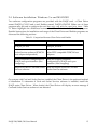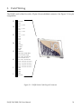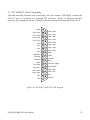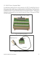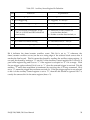
1
DAQP-208/208H/308
Type II PCMCIA
Data Acquisition Adapters
Users Manual
INTERFACE CARDS FOR PERSONAL COMPUTERS
OMEGA ENGINEERING, INC.
One Omega Drive
P.O. Box 4047
Stamford, CT 06907-4047
Tel: (203) 359-1660
Fax: (203) 359-7700
Toll free: 1-800-826-6342
E-mail: [email protected]
www.dasieee.com
WARRANTY/DISCLAIMER
OMEGA ENGINEERING, INC., warrants this unit to be free of defects in materials and workmanship for a period of 13
months from the date of purchase. OMEGA warranty adds an additional one (1) month grace period to the normal one (1)
year product warranty to cover shipping and handling time. This ensures that OMEGA’s customers receive maximum
coverage on each product. If the unit should malfunction, it must be returned to the factory for evaluation. OMEGA’s
Customer Service Department will issue an Authorized Return (AR) number immediately upon phone or written request.
Upon examination by OMEGA, if the unit is found to be defective it will be repaired or replaced at no charge. OMEGA’s
warranty does not apply to defects resulting from any action of the purchaser, including but not limited to mishandling,
improper interfacing, operation outside design limits, improper repair or unauthorized modification. This WARRANTY is
VOID if the unit shows evidence of having been tampered with or shows evidence of being damaged as a result of excessive
corrosion; or current, heat, moisture or vibration; improper specification; misapplication; misuse or other operating conditions
outside of OMEGA’s control. Components which wear are not warranted, including but not limited to contact points, fuses
and triacs.
OMEGA is pleased to offer suggestions on the use of its various products. However, OMEGA neither
assumes responsibility for any omissions or errors nor assumes liability for any damages that result from
the use of its products in accordance with information provided from OMEGA, either verbal or written.
OMEGA warrants only that the parts manufactured by it will be as specified and free of defects. OMEGA
MAKES NO OTHER WARRANTIES OR REPRESENTATIONS OF ANY KIND WHATSOEVER, EXPRESSED OR
IMPLIED, EXCEPT THAT OF TITLE, AND ALL IMPLIED WARRANTIES INCLUDING ANY WARRANTY OF
MERCHANTABILITY AND FITNESS FOR A PARTICULAR PURPOSE ARE HEREBY DISCLAIMED.
LIMITATION OF LIABILITY: The remedies of purchaser set forth herein are exclusive and the total
liability of OMEGA with respect to this order, whether based on contract, warranty, negligence,
indemnification, strict liability or otherwise, shall not exceed the purchase price of the component upon
which liability is based. In no event shall OMEGA be liable for consequential, incidental or special
damages.
CONDITIONS: Equipment sold by OMEGA is not intended to be used, nor shall it be used: (1) as a “Basic Component” under
10 CFR 21 (NRC), used in or with any nuclear installation or activity, medical application or used on humans. Should any
Product(s) be used in or with any nuclear installation or activity, medical application, used on humans or misused in any way,
OMEGA assumes no responsibility as set forth in our basic WARRANTY/DISCLAIMER language, and additionally, the
purchaser will indemnify OMEGA and hold OMEGA harmless from any liability or damage whatsoever arising out of the use
of the Product(s) in such a manner.
RETURN REQUESTS/INQUIRIES
Direct all warranty and repair requests/inquiries to the OMEGA Customer Service Department. BEFORE RETURNING ANY
PRODUCT(S) TO OMEGA, THE PURCHASER MUST OBTAIN AN AUTHORIZED RETURN (AR) NUMBER FROM OMEGA’S
CUSTOMER SERVICE DEPARTMENT (IN ORDER TO AVOID PROCESSING DELAYS). THE ASSIGNED NUMBER SHOULD
THEN BE MARKED ON THE OUTSIDE OF THE RETURN PACKAGE AND ON ANY CORRESPONDENCE. THE
PURCHASER IS RESPONSIBLE FOR SHIPPING CHARGES, FREIGHT, INSURANCE AND PROPER PACKAGING TO
PREVENT BREAKAGE IN TRANSIT.
FOR WARRANTY RETURNS, please have the following information available BEFORE contacting OMEGA:
(1) P.O. Number under which the product was purchased,
(2) Model and serial number of the product under warranty, and
(3) Repair instructions and/or specific problems relative to the product.
FOR NON-WARRANTY REPAIRS, consult OMEGA for current repair charges. Have the following information available
BEFORE contacting OMEGA:
(1) P.O. Number to cover the cost of the repair,
(2) Model and serial number of the product, and
(3) Repair instructions relative to the product.
OMEGA’s policy is to make running changes, not model changes, whenever an improvement is possible. This affords our
customers the latest in technology and engineering.
OMEGA is a registered trademark of OMEGA ENGINEERING, INC. © Copyright 1999 OMEGA ENGINEERING, INC. All
rights reserved. This document may not be copied, photocopied, reproduced, translated or reduced to any electronic medium
or machine readable form, in whole or in part, without prior written consent of OMEGA ENGINEERING, INC.
OMEGAnet? On-line Service:
DAQP-208/208H/308 Users Manual
Internet e-mail:
2
http://www.omega.com
[email protected]
Servicing North America :
USA:
ISO 9001 Certified
One Omega Drive, Box 4047
Stamford, CT 06907-0047
Tel: (203) 359-1660
E-mail: [email protected]
Canada:
976 Bergar
Laval (Quebec) H7L 5A1
Tel: (514) 856-6928
E-mail: [email protected]
FAX: (203) 359-7700
FAX: (514) 856-6886
For immediate technical or application assistance :
USA and Canada:
Sales Service: 1-800-826-6342 / 1-800-TC-OMEGA SM
Customer Service: 1-800-622-2378/ 1-800-622-BEST SM
Engineering Service: 1-800-872-9436 / 1-800-USA-WHEN SM
TELEX: 996404 EASYLINK: 62968934 CABLE: OMEGA
Mexico and Latin America:
Tel: (001) 800-826-6342
En Espanol: (001) 203-359-7803
FAX: (001) 203-359-7807
E-mail: [email protected]
Servicing Europe:
Benelux:
Postbus 8034, 1180 LA Amstelveen, The Netherlands
Tel: (31) 20 6418405
Toll Free in Benelux: 0800 0993344
E-mail: [email protected]
Czech Republic :
ul.Rude armady 1868, 733 01 Karvina-Hraniee
Tel: 42 (69) 6311899
FAX: 42 (69) 6311114
Toll Free: 0800-1-66342
E-mail: [email protected]
France:
9, rue Denis Papin, 78190 Trappes
Tel: (33) 130-621-400
Toll Free in France: 0800-4-06342
E-mail: [email protected]
Germany/Austria:
Daimlerstrasse 26, D-75392 Deckenpfronn, Germany
Tel: 49 (07056) 3017
Toll Free in Germany: 0130 11 21 66
E-mail: [email protected]
DAQP-208/208H/308 Users Manual
3
United Kingdom:
ISO 9002 Certified
One Omega Drive, River Bend Technology Drive
Northbank, Irlam, Manchester
M44 5EX, England
Tel: 44 (161) 777-6611
FAX: 44 (161) 777-6622
Toll Free in England: 0800-488-488
E-mail: [email protected]
It is the policy of OMEGA to comply with all worldwide safety and EMC/EMI regulations that apply.
OMEGA is constantly pursuing certification of it’s products to the European New Approach
Directives. OMEGA will add the CE mark to every appropriate device upon certification.
The information contained in this document is believed to be correct but OMEGA Engineering, Inc.
accepts no liability for any errors it contains, and reserves the right to alter specifications without
notice. WARNING: These products are not designed for use in, and should not be used for, patient
connected applications.
DAQP-208/208H/308 Users Manual
4
Notice
The information contained in this document cannot be reproduced in any form without the
written consent of Omega Engineering Inc. Any software programs accompanying this
document can be used only in accordance with any licensing agreement(s) between Omega
Engineering Inc. and the purchaser. Omega Engineering Inc. reserves the right to change this
documentation or the product to which it refers at any time and without notice.
The authors have taken due care in the preparation of this document and any associated
software program(s). Every attempt has been made to ensure accuracy and completeness.
Under no circumstances will Omega Engineering Inc. be liable for damages of any kind,
incidental or consequential, in regard to or arising from the performance or form of the
materials presented herein or in any software program(s) that may accompany this document.
Omega Engineering Inc. encourages and appreciates feedback concerning this document.
Please send any written comments to the Technical Support Department at the address listed
on the cover of this document.
Copyright ©2001
by Omega Engineering Inc.
All rights reserved. Printed in the U.S.A.
IBM®, PC® and PC-AT® are trademarks of the International Business Machines Corporation.
Windows®, MS-DOS®, Windows 95®, Windows 98®, Windows NT® and Windows 2000®
are trademarks of the Microsoft Corporation. Other product and company names are
registered trademarks or trademarks of their respective holders.
DAQP-208/208H/308 Users Manual
5
Table of Contents
1. Introduction
....................................................... 8
2. Hardware Configuration and Initial Setup
2.1
2.2
2.3
2.4
................. 9
Software Installation: Windows 95/98/2000 ® . . . . . . . . . . . . . . . . . . . . 9
2.1.1 Windows 2000 . . . . . . . . . . . . . . . . . . . . . . . . . . . . . . . . . . . . . . . . . . . . . . . . . . 9
2.1.2 Windows 98 . . . . . . . . . . . . . . . . . . . . . . . . . . . . . . . . . . . . . . . . . . . . . . . . . . . 10
2.1.3 Windows 95 . . . . . . . . . . . . . . . . . . . . . . . . . . . . . . . . . . . . . . . . . . . . . . . . . . . 10
2.1.4 Viewing Resources with Device Manager . . . . . . . . . . . . . . . . . . . . . . . . . 11
Software Installation: Windows NT 4.0 ® . . . . . . . . . . . . . . . . . . . . . . . . 11
Data Acquisition Software and Drivers . . . . . . . . . . . . . . . . . . . . . . . . . . 12
Software Installation: Windows 3.x and MS-DOS® . . . . . . . . . . . . . . 13
2.4.1 Client Driver for MS-DOS . . . . . . . . . . . . . . . . . . . . . . . . . . . . . . . . . . . . . . . 14
2.4.2 Enabler for MS-DOS . . . . . . . . . . . . . . . . . . . . . . . . . . . . . . . . . . . . . . . . . . . . 18
3. Field Wiring
. . . . . . . . . . . . . . . . . . . . . . . . . . . . . . . . . . . . . . . . . . . . . . . . . . . . . . . 21
3.1 UIO-37 Screw Terminal Block . . . . . . . . . . . . . . . . . . . . . . . . . . . . . . . . . . . . 22
3.2 CP-DAQPA Cable Assembly . . . . . . . . . . . . . . . . . . . . . . . . . . . . . . . . . . . . 23
4. Theory of Operation
............................................
4.1 DC/DC Power Supply . . . . . . . . . . . . . . . . . . . . . . . . . . . . . . . . . . . . . . . . . . .
4.2 Analog Input Multiplexer . . . . . . . . . . . . . . . . . . . . . . . . . . . . . . . . . . . . . . . .
4.3 Programmable Gain Control Amplifier . . . . . . . . . . . . . . . . . . . . . . . . . .
4.4 Scan List Register . . . . . . . . . . . . . . . . . . . . . . . . . . . . . . . . . . . . . . . . . . . . . . . .
4.5 Trigger Circuit . . . . . . . . . . . . . . . . . . . . . . . . . . . . . . . . . . . . . . . . . . . . . . . . . . .
4.6 A/D Converter and Data FIFO . . . . . . . . . . . . . . . . . . . . . . . . . . . . . . . . . .
4.7 Interrupt and Status . . . . . . . . . . . . . . . . . . . . . . . . . . . . . . . . . . . . . . . . . . . . . .
4.8 Digital I/O . . . . . . . . . . . . . . . . . . . . . . . . . . . . . . . . . . . . . . . . . . . . . . . . . . . . . . .
4.9 A/D State Machine . . . . . . . . . . . . . . . . . . . . . . . . . . . . . . . . . . . . . . . . . . . . . .
4.10 D/A Circuit . . . . . . . . . . . . . . . . . . . . . . . . . . . . . . . . . . . . . . . . . . . . . . . . . . . . .
4.11 Timer/Counter . . . . . . . . . . . . . . . . . . . . . . . . . . . . . . . . . . . . . . . . . . . . . . . . .
5. I/O Registers
.....................................................
5.1 PCMCIA Interface . . . . . . . . . . . . . . . . . . . . . . . . . . . . . . . . . . . . . . . . . . . . . . . .
5.1.1 Configuration and Option Register (COR) . . . . . . . . . . . . . . . . . . . . . . . . .
5.1.2 Card Configuration and Status Register (CCSR) . . . . . . . . . . . . . . . . . . . .
DAQP-208/208H/308 Users Manual
25
25
26
26
27
28
29
30
30
31
32
32
34
34
35
35
6
5.2 Address Map . . . . . . . . . . . . . . . . . . . . . . . . . . . . . . . . . . . . . . . . . . . . . . . . . . . . . 36
5.2.1 Data FIFO Register (base + 0) . . . . . . . . . . . . . . . . . . . . . . . . . . . . . . . . . . . .
5.2.2 Scan List Queue Register (base + 1) . . . . . . . . . . . . . . . . . . . . . . . . . . . . . .
5.2.3 Status Register (base + 2) . . . . . . . . . . . . . . . . . . . . . . . . . . . . . . . . . . . . . . . .
5.2.4 Digital I/O Register . . . . . . . . . . . . . . . . . . . . . . . . . . . . . . . . . . . . . . . . . . . .
5.2.5 Pacer Clock (base + 4, + 5, + 6) . . . . . . . . . . . . . . . . . . . . . . . . . . . . . . . . . . .
5.2.6 Command Register (base + 7) . . . . . . . . . . . . . . . . . . . . . . . . . . . . . . . . . . . .
5.2.7 D/A Data Port (base + 8, base + 9) . . . . . . . . . . . . . . . . . . . . . . . . . . . . . . .
5.2.8 Timer/Counter Port (base + 10, base + 11) . . . . . . . . . . . . . . . . . . . . . . . .
5.2.9 Auxiliary Control Register (base + 15) . . . . . . . . . . . . . . . . . . . . . . . . . . . .
5.2.10 Auxiliary Status Register (base + 15) . . . . . . . . . . . . . . . . . . . . . . . . . . . . .
6.
Specifications
37
39
44
45
46
47
49
51
53
53
. . . . . . . . . . . . . . . . . . . . . . . . . . . . . . . . . . . . . . . . . . . . . . . . . . . . . 55
DAQP-208/208H/308 Users Manual
7
List of Figures and Tables
Figure 3-1. DAQP Series Card Output Connector . . . . . . . . . . . . . . . . . . . . . . . . . . . . . . . . . . . .
Figure 3-2. CP-DAQPA/UIO-37 D37 Pin Diagram . . . . . . . . . . . . . . . . . . . . . . . . . . . . . . . . . . .
Figure 3-3. UIO-37 Terminal Block . . . . . . . . . . . . . . . . . . . . . . . . . . . . . . . . . . . . . . . . . . . . . . . .
Figure 3-4. DAQP Card with Accessories . . . . . . . . . . . . . . . . . . . . . . . . . . . . . . . . . . . . . . . . . . .
Figure 4-1. Transition Diagram of A/D Conversion Process . . . . . . . . . . . . . . . . . . . . . . . . . . .
Figure 5-1. Pacer Clock Block Diagram . . . . . . . . . . . . . . . . . . . . . . . . . . . . . . . . . . . . . . . . . . . . .
21
22
23
24
31
46
Table 2-1. Comparison Between Client Driver and Enabler . . . . . . . . . . . . . . . . . . . . . . . . . . .
Table 3-1. DAQP Series Card Cable Mapping . . . . . . . . . . . . . . . . . . . . . . . . . . . . . . . . . . . . . . .
Table 5-1. PCMCIA Configuration Registers . . . . . . . . . . . . . . . . . . . . . . . . . . . . . . . . . . . . . . . .
Table 5-2. COR Bit Definition . . . . . . . . . . . . . . . . . . . . . . . . . . . . . . . . . . . . . . . . . . . . . . . . . . . . .
Table 5-3. CCSR Bit Definition . . . . . . . . . . . . . . . . . . . . . . . . . . . . . . . . . . . . . . . . . . . . . . . . . . . .
Table 5-4. DAQP Series Card Address Map . . . . . . . . . . . . . . . . . . . . . . . . . . . . . . . . . . . . . . . . .
Table 5-5. Data FIFO Register Bit Allocation . . . . . . . . . . . . . . . . . . . . . . . . . . . . . . . . . . . . . . . .
Table 5-6. Data FIFO Operation Mode . . . . . . . . . . . . . . . . . . . . . . . . . . . . . . . . . . . . . . . . . . . . .
Table 5-7. Data FIFO Threshold Setting . . . . . . . . . . . . . . . . . . . . . . . . . . . . . . . . . . . . . . . . . . . .
Table 5-8. Data FIFO Flag Status . . . . . . . . . . . . . . . . . . . . . . . . . . . . . . . . . . . . . . . . . . . . . . . . . .
Table 5-9. Scan List Queue Entry Bit Definition . . . . . . . . . . . . . . . . . . . . . . . . . . . . . . . . . . . . .
Table 5-10. Scan List Queue Programming Example 1 . . . . . . . . . . . . . . . . . . . . . . . . . . . . . . . .
Table 5-11. Scan List Queue Programming Example 2 . . . . . . . . . . . . . . . . . . . . . . . . . . . . . . . .
Table 5-12. Control Register Bit Definition . . . . . . . . . . . . . . . . . . . . . . . . . . . . . . . . . . . . . . . . . .
Table 5-13. Status Register Bit Definition . . . . . . . . . . . . . . . . . . . . . . . . . . . . . . . . . . . . . . . . . . .
Table 5-14. Digital Output Register Bit Definition . . . . . . . . . . . . . . . . . . . . . . . . . . . . . . . . . . .
Table 5-15. Digital Input Register Bit Definition . . . . . . . . . . . . . . . . . . . . . . . . . . . . . . . . . . . . .
Table 5-16. Command Register Bit Definition . . . . . . . . . . . . . . . . . . . . . . . . . . . . . . . . . . . . . . .
Table 5-17. Data FIFO Threshold Setting . . . . . . . . . . . . . . . . . . . . . . . . . . . . . . . . . . . . . . . . . . .
Table 5-18. D/A Data Port Bit Definition . . . . . . . . . . . . . . . . . . . . . . . . . . . . . . . . . . . . . . . . . . .
Table 5-19. D/A Update Modes . . . . . . . . . . . . . . . . . . . . . . . . . . . . . . . . . . . . . . . . . . . . . . . . . . .
Table 5-20. Timer/Counter Modes . . . . . . . . . . . . . . . . . . . . . . . . . . . . . . . . . . . . . . . . . . . . . . . .
Table 5-21. Auxiliary Control Register Bit Definition . . . . . . . . . . . . . . . . . . . . . . . . . . . . . . . . .
Table 5-22. Auxiliary Status Register Bit Definition . . . . . . . . . . . . . . . . . . . . . . . . . . . . . . . . . .
13
24
34
35
35
36
37
37
38
39
39
40
40
41
44
45
45
47
48
49
50
51
53
54
DAQP-208/208H/308 Users Manual
8
1. Introduction
DAQP series cards are PCMCIA type II data acquisition adapters with 4 differential or 8
single-ended analog input channels. The number of input channels can be expanded to 128
when used with input expansion cards. DAQP series products include the DAQP-208, the
DAQP-208H and the DAQP-308. Card features include:
? Sampling rate up to 100 kHz with 12 or 16 bit resolution
? 4 differential or 8 single-ended analog input channels, expandable to 128 channels
? Two 12 bit D/A channels with direct or synchronized update
? Bipolar input range up to ±10 volts with programmable gain of 1, 2, 4 or 8
(DAQP-208/308) or gain of 1, 10, 100 or 1000 (DAQP-208H)
? Programmable scan list with up to 2048 channel and gain entries, plus selectable scan
speed of 10, 20 or 40 µs
? Additional 16 bit timer/counter with auto reload, read-out/overflow latches and
internal/external gate control and clock sources
? Software, TTL or analog trigger with
programmable threshold and
pre-trigger capability
Equipped with a 4K data FIFO, the
DAQP card can achieve high speed data
acquisition under various operating
platforms. Also equipped with a 2048
entry scan FIFO, the DAQP supports full
speed, random order channel scanning
and gain selection for all input channels
including expansion channels.
The DAQP card uses a 24-bit pacer clock and a programmable divide-by-2, by-10 or by-100
pre-scaler. The pacer clock can be used with either an internal or external clock source.
DAQP series cards are also equipped with two independent 12 bit D/A output channels with
a bipolar range of -5 to +5 volts. D/A channels can be updated directly when writing the
corresponding D/A port (direct mode) or simultaneously with a synchronization signal.
DAQP-208/208H/308 Users Manual
9
2. Hardware Configuration and Initial Setup
2.1 Software Installation: Windows 95/98/2000 ®
An “INF” file (daqpcard.inf) is included on the root directory of the DaqSuite CD to allow easy
configuration in the Windows environment. Windows uses the “INF” file to determine the
system resources required by the DAQP card, searches for available resources to fill the
requirements and then updates the Windows hardware registry with entries to allocate the
resources. Follow the instructions below to configure your DAQP series card under
Windows.
Card Information Structure (CIS) Differences
DAQP series cards come with 12 and 16 bit versions. Each version may also have different
product names and descriptions depending on the manufacturer or vendor name associated
with the card. This results in differences in the CIS for the specific DAQP card version.
Windows will configure the DAQP card in the same manner regardless of CIS differences. It is
strongly recommended that the DaqSuite CD “INF” file be used to configure the DAQP card
and that it should only be used if Windows 95/98/2000 does not recognize the card upon
insertion. It is not necessary to install the INF file if Windows recognizes the card when
inserted due to the presence of an older INF file in the system. Do not try to modify, merge,
rename or delete the system INF files. If difficulties are encountered during installation,
contact the technical support department at the number shown on the cover of this manual.
2.1.1 Windows 2000
1. Insert the DAQP card into any available PC Card socket. The first time a new PC
Card type is installed the “New Hardware Found” window will open. Click Next
to continue.
2. The New Hardware Found window provides several options to configure the
DAQP card. Select the “Search for a suitable driver for my device” radio button.
Click Next to continue.
3. Insert the DaqSuite CD, select the “CD-ROM drive” check box and click Next to
continue. Windows 2000 will browse the CD until it finds the file ”x:\daqpcard.inf“,
where “x” is the CD-ROM drive letter. Click Next to continue.
4. When Windows finishes the configuration process, click Finish to exit the New
Hardware Found Wizard.
5. Hardware Configuration is not complete until the user has run the desired driver
support installation from the DaqSuite CD demo. This support installation is
required to install Windows 2000 drivers for your DAQP card. Refer to Section 2.3:
Data Acquisition Software and Drivers for a list of driver installation options.
DAQP-208/208H/308 Users Manual
10
2.1.2 Windows 98
1. Insert the DAQP card into any available PC Card socket. The first time a new PC
Card type is installed the “Add New Hardware Wizard” window will open. Click
Next to continue.
2. The Add New Hardware Wizard provides several options to configure the DAQP
card. Select the recommended option radio button: “Search for the best driver for
your device”. Click Next to continue.
3. An Install from Disk dialog box will open. Insert the DaqSuite CD, either type in or
browse for the correct CD-ROM drive letter and then click OK. Windows 98 will
browse the CD until it finds the file ”x:\daqpcard.inf“, where “x” is the CD-ROM
drive letter. Click Next to continue.
4. When Windows finishes the configuration process, click Finish to exit the New
Hardware Found Wizard.
5. Hardware configuration is not complete until the user has run the desired driver
support installation from the DaqSuite CD demo. This support installation is
required to install Windows 98 drivers for your DAQP card. Refer to Section 2.3:
Data Acquisition Software and Drivers for a list of driver installation options.
2.1.3 Windows 95
1. Insert the DAQP card into any available PC Card socket. The first time a new PC
Card type is installed the “New Hardware Found” window will open. Select the
“Driver from disk provided by hardware manufacturer” radio button and click OK
to continue.
2. An Install from Disk dialog box will open. Insert the DaqSuite CD, either type in or
browse for the correct CD-ROM drive letter and then click OK. Windows 95 will
browse the CD until it finds the file ”x:\daqpcard.inf“, where “x” is the CD-ROM
drive letter and then proceed to configure the hardware.
3. Hardware configuration is not complete until the user has run the desired driver
support installation from the DaqSuite CD demo. This support installation is
required to install Windows 95 drivers for your DAQP card. Refer to Section 2.3:
Data Acquisition Software and Drivers for a list of driver installation options.
DAQP-208/208H/308 Users Manual
11
2.1.4 Viewing Resources with Device Manager
Follow the instructions provided here to view resources used by the DAQP card using the
“Device Manager” utility in Windows.
1. Double click the My Computer icon located on the Windows desktop and then
double click the Control Panel icon. Double click the System icon to open the
System Properties window.
2. Click the “Device Manager” tab located at the top of the dialog box. (Windows 2000
users must click the “Hardware” tab and then press the “Device Manager” button).
The Device Manager lists all hardware devices inside the Windows registry.
Additional information is available on any of these devices by clicking on the
device name and then selecting the Properties button.
3. Double click the device group “Data_ Acquisition”. The DAQP card model name
should appear on the list below this category. Double click on the model name to
open the Hardware Properties window.
4. Click the Resources tab located along the top of the dialog box to view the resources
Windows has allocated to the DAQP card.
2.2 Software Installation: Windows NT 4.0 ®
Windows NT 4.0 does not use the “Add New Hardware” wizard to configure new hardware.
Once the DAQP card is installed, run the desired driver support installation from the
DaqSuite CD demo to install Windows NT 4.0 drivers. During the installation process, NT 4.0
registry entries are created to automatically start and run your hardware. Refer to Section 2.3:
Data Acquisition Software and Drivers for a list of driver installation options. After installing
the drivers, the base address and IRQ level must be determined and saved in the
corresponding configuration file for the resources to be assigned to the device. Determine
what I/O Port number and IRQ levels are available from the windows NT diagnostics. Save
these to the device's configuration file (see section 2.2 in the daqdrive manual for a description
on how to use the configuration utility). You must reboot at this point for these setting to take
effect and to determine installation success. To determine if your DAQP card is correctly
installed and to view its assigned resources, follow the instructions listed below.
1. From within Windows NT 4.0 , Select Start | Programs | Administrative Tools
(Common) | Windows NT Diagnostics.
2. When the Windows NT Diagnostics window opens, click the “Resources” tab
located at the top of the dialog box. Press the Devices button located in the bottom
right corner. The DAQP card driver name is “DAQPDRV”. This name should be
listed under the category “Device”.
3. To view the resources assigned to the DAQP card, press the IRQ and I/O Port
buttons at the bottom of the Windows NT Diagnostics window.
DAQP-208/208H/308 Users Manual
12
To remove the DAQP card from your Windows NT 4.0 system, run the associated driver
support uninstallation program using the Add/Remove Programs icon located in the
Control Panel folder. (This will remove all registry entries applicable to your hardware).
When the uninstallation is complete, shut down your computer and remove the hardware. To
verify these actions, reboot and follow steps 1 and 2 above to ensure the “DAQPDRV” listing
no longer appears under the “Device” category.
DAQP-208/208H/308 Users Manual
13
2.3 Data Acquisition Software and Drivers
Data acquisition software and driver support installations are available from the DaqSuite CD
demo main menu.
1. Quatech’s DaqEZ? - This software package was specifically designed to support
all Quatech’s data acquisition adapter functions and is included free of charge with
your hardware. DaqEZ is an easy to use application that requires no programming
knowledge and allows the user to graphically acquire and display real time data
using customized channel labels, charts and displays. (Includes hardware drivers
for Windows 95 or 98).
2. DASYTEC’s DASYLab - DASYLab is designed to solve sophisticated data
acquisition and control tasks quickly. Module symbols representing
inputs/outputs, display instruments or operations to be performed are inserted
into a work sheet and graphically connected. This approach allows complex
applications to be constructed without programming knowledge.
The DaqSuite CD includes a fully functional 30 day evaluation version of DASYLab.
(Includes hardware drivers for Windows 95, 98, 2000 and NT 4.0).
3. 3rd Party Driver Support - Hardware drivers for Windows 95, 98, 2000 and NT
4.0 are available for the following 3rd party data acquisition software packages:
DASYLab from DASYTEC? - Run this installation if DASYLab software is already
installed on the system that will use your Quatech hardware.
LabVIEW? from National Instruments?
- Run this installation if LabVIEW
software is already installed on the system that will use your Quatech hardware.
TestPoint? from Capital Equipment Corporation - Run this installation if TestPoint
software is already installed on the system that will use your Quatech hardware.
4. Drivers/Programming Support - Quatech’s Daqdrive? provides hardware
drivers, a hardware configuration utility and data acquisition programming
examples for Microsoft? and Borland? C/C++, Visual Basic? and Borland
Dephi? . (Includes hardware drivers for Windows 95, 98, 2000 and NT 4.0).
DAQP-208/208H/308 Users Manual
14
2.4 Software Installation: Windows 3.x and MS-DOS®
Two software configuration programs are provided with the DAQP card: a Client Driver
named DAQPA_CL.SYS and a card Enabler named DAQPA_EN.EXE. Either one of these
programs may be used to configure the card but only one may be used at a time. Table
2-1 below highlights the differences between the Client Driver and the Enabler programs.
Detailed instructions for installation and usage of the Client Driver and Enabler programs are
discussed the following sections.
Table 2-1. Comparison Between Client Driver and Enabler
Client Driver
Enabler
DAQPA_CL.SYS
DAQPA_EN.EXE
Interfaces to PCMCIA Card and
Socket Services software (PCMCIA
host adapter independent)
Interfaces directly to Intel 82365SL and
other PCIC compatible PCMCIA host
adapters
Allows automatic configuration of
DAQP card upon insertion (Hot
Swapping)
Does not support automatic
configuration of DAQP card upon
insertion (Hot Swapping)
Requires PCMCIA Card and Socket
Services software
Does not require PCMCIA Card and
Socket Services software
On systems with Card and Socket Services installed, the Client Driver is the preferred method
of installation. To determine if Card and Socket Services software is installed, install the
DAQP series Client Driver. When loaded, the Client Driver will display an error message if
Card and Socket Services software is not detected.
DAQP-208/208H/308 Users Manual
15
2.4.1 Client Driver for MS-DOS
For systems using MS-DOS and PCMCIA Card and Socket Services software, a Client Driver
named “DAQPA_CL.SYS” is provided to configure the DAQP series cards. PCMCIA Card
and Socket Services software is not provided with your DAQP card, but is available from your
vendor.
Some versions of Card and Socket Services dated before 1993 do not support general purpose
I/O cards. After careful installation of the Client Driver, if the DAQP card still does not
configure or operate properly, an updated version of Card and Socket Services software may
be required. The following procedures are used to install the DAQP series Client Driver:
1. Copy the file DAQPA_CL.SYS located in the PCMCIA\DOS\CLIENTS directory of the
DaqSuite CD onto the root directory of the system hard drive.
2. Using an ASCII text editor, open the system's CONFIG.SYS file located in the root
directory of the boot drive.
3. Locate the line in the CONFIG.SYS file where Card and Socket Services software is
installed.
4. AFTER the line installing the Card and Socket Services software, add the following line
to the CONFIG.SYS file:
DEVICE = drive:\DAQPA_CL.SYS (options)
where (options) are the DAQP series Client Driver command line options discussed on
the following pages.
5. Save the CONFIG.SYS file and exit the text editor.
6. Insert the DAQP card into one of the system PCMCIA slots.
NOTE: Since the DAQP series Client Driver supports "Hot Swapping", it is not
necessary to have the DAQP card installed when booting the system. By inserting the
card before booting, the Client Driver will report the card configuration during the boot
process and thereby verify changes made to CONFIG.SYS.
7. Reboot the system and note the message displayed when the Client Driver is loaded. If
the Client Driver reports an “invalid command line option”, correct the entry in the
CONFIG.SYS file and reboot the system again. If the Client Driver reports “Card and
Socket Services not found”, then either Card and Socket Services software must be
installed on the system or the DAQP series Enabler program must be used to configure
the card. If the Client Driver reports the desired card configuration, the installation
process is complete and the DAQP card may be removed and inserted from the system
as desired. On each insertion into the PCMCIA socket, the DAQP card will
automatically be reconfigured to the specified settings.
DAQP-208/208H/308 Users Manual
16
2.4.1.1 Client Driver Command Line Options
The DAQP series Client Driver accepts up to eight command line arguments from the user to
determine the configuration of the DAQP card. If any arguments are provided, the Client
Driver will attempt to configure any DAQP card with the options specified in the order they
are entered on the command line. Each argument must be enclosed in parenthesis and must
be separated from other arguments by a space in the command line. Inside an argument, a
comma (no space) should be used to separate the parameters from each other if there are two
or more parameters. Within each argument, any or all of the following parameters may be
specified:
b address
Specifies the base I/O address of the DAQP card in hexadecimal. “Address”
must be in the range 100H - 3F8H and must reside on an even 8-byte boundary
(“address” must end in 0 or 8). If this option is omitted, a base address will be
assigned by Card and Socket Services software.
i
irq
Specifies the interrupt level (IRQ) of the DAQP card in hexadecimal. “Irq” must
be one of the following values: 3, 4, 5, 7, 9, 10, 11, 12, 14, 15 or 0 if no IRQ if
desired. If this option is omitted, an interrupt level will be assigned by Card
and Socket Services software.
s socket
Specifies the PCMCIA socket number to configure. “Socket” must be in the
range 0 - 15. If this option is omitted, the configuration argument will be applied
to any available DAQP card inserted into any socket in the system.
2.4.1.2 Client Driver Installation Examples
With the Client Driver, the user may specify a list of selections (in the form of command line
arguments) for the configuration of the DAQP series cards. The Client Driver scans this list
from left to right until it finds a selection that is currently available in the system. If none of the
preferred selections are available, the Client Driver requests a configuration from Card and
Socket Services software.
Example 1
DEVICE = C:\DAQPA_CL.SYS
In example 1, no command line arguments are specified. The Client Driver will configure the
DAQP card into ANY socket with a base address and IRQ level assigned by Card and Socket
Services.
Example 2
DEVICE = C:\DAQPA_CL.SYS (b300)
In this example, a single command line argument is provided. The Client Driver will attempt
to configure a DAQP card inserted into ANY socket with a base address of 300H and an IRQ
level assigned by Card and Socket Services. If the base address 300H is not available, the
DAQP card will NOT be configured.
DAQP-208/208H/308 Users Manual
17
Example 3
DEVICE = C:\DAQPA_CL.SYS (s0,b300,i5)
Example 3 is also a single command line argument. The client Driver will attempt to configure
the DAQP card inserted in socket 0 at base address 300H and IRQ level 5. If either address
300H or IRQ level 5 is unavailable, the card will NOT be configured. In addition, the Client
Driver will NOT configure any DAQP card inserted into any socket except socket 0.
Example 4
DEVICE = C:\DAQPA_CL.SYS (b300,i5) (i10) ( )
Three command line arguments are provided in this example. The Client Driver will first
attempt to configure a DAQP card inserted into any socket with a base address 300H and IRQ
level 5. If either address 300H or IRQ level 5 is unavailable, the Client Driver will proceed to
the second command line argument and attempt to configure the card with a base address
assigned by the Card and Socket Services and IRQ level 10. If IRQ level 10 is also unavailable,
the Client Driver will then go to the third command line argument and attempt to configure it
with a base address and an IRQ level assigned by Card and Socket Services.
Example 5
DEVICE = C:\DAQPA_CL.SYS (b300,i5) ( ) (i10)
The difference between example 5 and example 4 is the order of the second and third
command line arguments. The Client Driver will first attempt to configure a DAQP card
inserted into any socket with a base address 300H and IRQ level 5. If either address 300H or
IRQ level 5 is unavailable, the Client Driver will proceed to the second command line
argument and attempt to configure the card with a base address and IRQ level assigned by
Card and Socket Services. Since the second command line argument includes all available
address and IRQ resources, the third command line argument will never be reached by the
Client Driver. The user must ensure command line arguments are placed in a logical order.
Example 6
DEVICE = C:\DAQPA_CL.SYS (s0,b300,i5) (s1,b310,i10)
There are two command line arguments in example 6, which is desirable in systems where
two or more DAQP cards are to be installed. The Client Driver will attempt to configure the
DAQP card in socket 0 with base address 300H and IRQ 5. If there is a DAQP card in socket 1,
it will be configured with base address 310H and IRQ 10. This allows the user to force the card
address and IRQ settings to be socket specific as required by software or cable connections. If
the requested resources are not available, the DAQP cards will not be configured.
DAQP-208/208H/308 Users Manual
18
2.4.1.3 Common Problems
Generic Client Drivers
Many Card and Socket Services packages include a generic client driver (or SuperClient)
which configures standard I/O devices. If one of these generic client drivers is installed, it
may configure the DAQP card and cause the DAQP series Client Driver to fail installation. If
this is the case, try the following:
Modify the operation of the generic client driver so that it will not configure the DAQP
card by placing the DAQP series Client Driver before the generic client driver in the
CONFIG.SYS file. Consult the Card and Socket Services documentation for availability
and details of this feature.
Available Resources
One function of Card and Socket Services software is to track which system resources
(memory addresses, I/O addresses, IRQ levels, etc.) are available for assignment to inserted
PCMCIA cards. Sometimes, however, the Card and Socket Services assumes or incorrectly
determines that a particular resource is unavailable when it actually is available. Most Card
and Socket Services generate a resource table, typically in the form of an “.INI” file, which the
user can modify to adjust the available system resources. Consult the Card and Socket
Services documentation for the availability and details of this feature.
Multiple Configuration Attempts
Some Card and Socket Services have a setting which aborts the configuration process after a
single configuration failure (such as a configuration request for an unavailable resource). The
user should change this setting to allow for multiple configuration attempts. Consult the Card
and Socket Services documentation for the availability and details of this feature.
Older Versions of Card and Socket Services
Some versions of Card and Socket Services dated before 1993 do not support general purpose
I/O cards like the DAQP series PC cards. If after careful installation of the DAQP series Client
Driver the DAQP card still can not be configured or operated properly, an updated version of
Card and Socket Services may be required.
DAQP-208/208H/308 Users Manual
19
2.4.2 Enabler for MS-DOS
For systems that are not operating PCMCIA Card and Socket Services software, the DAQP
series card includes an Enabler program to enable and configure the DAQP card. This
Enabler, DAQPA_EN.EXE, will operate in any DOS system using an Intel 82365SL or PCIC
compatible PCMCIA host adapter.
In order to use the DAQP series Enabler for DOS, the system must NOT be configured with
Card and Socket Services software. If Card and Socket Services software is installed, the
Enabler may interfere with its operation and the devices it controls. Therefore use either the
DAQP series Client Driver or Enabler exclusively.
The DAQP series Enabler does not support automatic configuration of PCMCIA cards upon
insertion, more commonly referred to as “Hot Swapping”. This means the card must be
installed in one of the system's PCMCIA sockets before executing DAQPA_EN.EXE. If more
than one adapter is installed in a system, the Enabler must be executed separately for each
card. Furthermore, DAQPA_EN.EXE should be executed to release the resources used by the
card before it is removed from the PCMCIA socket. Since PCMCIA cards do not retain their
configuration after removal, any card removed from the system must be reconfigured with the
Enabler after being reinserted into it’s PCMCIA socket.
The Enabler requires a region of high DOS memory when configuring the DAQP card. This
region is 1000H (4096) bytes long and by default begins at address D0000H (it may be changed
by the “w” option as described in following sections). If a memory manager such as EMM386,
QEMM or 386MAX is installed on the system, this region of DOS memory must be excluded
from the memory manager’s control (normally by using the “x” switch). Consult the
documentation provided with the memory manager software for instructions on how to
exclude this memory region. Follow the procedures listed here to install the DAQP Enabler:
1. Copy the file DAQPA_EN.EXE located in the PCMCIA\DOS\Enablers directory of the
DaqSuite CD onto the root directory of the system hard drive.
2. Using an ASCII text editor, open the system's CONFIG.SYS file located in the root
directory of the boot drive.
3. Add the following line to the CONFIG.SYS file:
DEVICE = drive:\DAQPA_EN.EXE (options)
where (options) are the DAQP series Enabler command line options discussed on the
following pages. Save the CONFIG.SYS file and exit the text editor.
4. Insert the DAQP card into one of the system PCMCIA slots. NOTE: Since the DAQP
series Enabler does not support "Hot Swapping", it is necessary to have the DAQP card
installed when booting the system.
DAQP-208/208H/308 Users Manual
20
6. Reboot the system and note the message displayed when the Enabler is loaded. If the
Enabler reports the desired card configuration, the installation process is complete.
DAQP-208/208H/308 Users Manual
21
2.4.2.1 Enabler Command Line Options
To configure a DAQP series card, the Enabler requires one command line argument from the
user to determine the configuration. This argument must be enclosed in parenthesis. Within
the argument, a comma (no space) must be used to separate the parameters from each other if
there are two or more parameters. The following parameters may be specified in the
command line argument:
s socket
Specifies the PCMCIA socket number to configure. “Socket” must be in the
range 0 - 15. This option is always required.
b address
Specifies the base I/O address of the DAQP card in hexadecimal. “Address”
must reside on an even 8-byte boundary (“address” must end in 0 or 8). This
option is required if the “r” option is not used.
i
Specifies the interrupt level (IRQ) of the DAQP card in hexadecimal. “Irq” must
be one of the following values: 3, 4, 5, 7, 9, 10, 11, 12, 14, 15, or 0 if no IRQ is
desired. This option is required if the “r” option is not used.
irq
w address Specifies the base address of the memory window required to configure the
DAQP card. Set “address”= D0 for a memory window at D0000, D8 for a
memory window at D8000, etc. Valid settings for address are C8, CC, D0, D4,
D8, and DC. If omitted, “address” = D0 is assumed.
r
Instructs the Enabler to release the resources previously allocated to the DAQP
card. When this option is used, B address and I irq options will be ignored.
Therefore, do NOT use this option when initially configuring the DAQP card.
2.4.2.2 Enabler Examples
Example 1
DEVICE = C:\DAQPA_EN.EXE
No command line argument is specified. The Enabler will report an error and display the
proper usage of the Enabler.
Example 2
DEVICE = C:\DAQPA_EN.EXE (s0,b300,i5)
In this example, the Enabler will configure the DAQP card in socket 0 with a base address
300H and IRQ level 5 using a configuration memory window at D0000H.
Example 3
DEVICE = C:\DAQPA_EN.EXE (i10,b310,s1)
In example 3, the Enabler will configure the DAQP card in socket 1 with a base address at
310H and IRQ level 10 using a configuration memory window at D0000H. Note the parameter
order is not significant.
DAQP-208/208H/308 Users Manual
22
Example 4
DEVICE = C:\DAQPA_EN.EXE (s0,b300,i5,wCC)
Here the Enabler will configure the DAQP card in socket 0 with a base address at 300H and
IRQ level 5 using a configuration memory window at CC000H.
Example 5
DEVICE = C:\DAQPA_EN.EXE (s0,r)
DEVICE = C:\DAQPA_EN.EXE (s0,r,b300,i5)
These two command line arguments are equivalent because of the “r” option. The Enabler
will release the configuration used by the DAQP card in socket 0 using a configuration
memory window at D0000H.
Example 6
DEVICE = C:\DAQPA_EN.EXE (s0,r,wC8)
Here the Enabler will release the configuration used by the DAQP card in socket 1, using a
configuration memory window at C8000H.
2.4.2.3 Common Problems
Memory Range Exclusion
The Enabler requires a region of high DOS memory when configuring a DAQP card. This
region is 1000H (4096) bytes long and by default begins at address D0000H (this default
address can be changed by using the “w” option).
If a memory manager such as EMM386, QEMM or 386MAX is installed on the system, this
region of DOS memory must be excluded from the memory manager’s control (normally by
using the “x” switch). Consult the documentation provided with the memory manager
software for instructions on how to exclude this memory region.
Furthermore, some systems use the high memory area for ROM shadowing to improve
overall system performance. For the Enabler to properly operate, any ROM shadowing must
be disabled in the address range specified for the configuration window. This can usually be
completed by using the system’s CMOS setup utility.
Socket Numbers
The Enabler requires that the socket number be specified for the DAQP card to be configured.
The DAQP card must be inserted into the socket before executing the Enabler.
For the DAQP series Enabler, the lowest socket number is always designated as socket 0 and
the highest socket number as N-1, (assuming there are N sockets available). Some vendors
number their sockets from 1 to N. In that case, the vendor socket number minus 1 should be
used in the “s” option for the DAQP series Enabler.
Card and Socket Services Software
In order to use DAQP series Enabler for DOS, the system must NOT be configured with Card
and Socket Services software. If Card and Socket Services software is installed, the Enabler
may interfere with its operation and the devices it controls.
DAQP-208/208H/308 Users Manual
23
3. Field Wiring
The DAQP card is fitted in with a 32-pin 0.8 mm shielded connector. See Figure 3-1 for pin
assignments.
33
30
25
20
15
10
5
1
Reserved
Ch 0
Ch 0 (-) / Ch 4
Ch 1
Ch 1 (-) / Ch 5
Ch 2
Ch 2 (-) / Ch 6
Ch 3
Ch 3 (-) / Ch 7
GND
DA0
DA1
+5V
GND
ExtClock
ExtGate
ExtOut
GND
FullPower
SSH (Synch. Sample Hold)
DI 0 / External Trigger
DI 1 / GS 0 (Ext. Gain Sel.
DI 2 / External Clock
DI 3 / GS 1 (Ext. Gain Sel.
DO 0 / CS0 (Ext. Chn. Sel. 0)
DO 1 / CS1 (Ext. Chn. Sel. 1)
DO 2 / CS2 (Ext. Chn. Sel. 2)
DO 3 / CS3 (Ext. Chn. Sel. 3)
GND
GND
GND
GND
Reserved
Figure 3-1. DAQP Series Card Output Connector
DAQP-208/208H/308 Users Manual
24
3.1 CP-DAQPA Cable Assembly
The cable assembly included with your DAQP card, part number CP-DAQPA, converts the
card’s 32 pin I/O connector to a standard D37 connector. Figure 3-2 illustrates the D37
connector pin assignments for the CP-DAQPA and the optional screw terminal block UIO-37.
GND
19
Ch0- / Ch4
18
Ch1- / Ch5
17
Ch2- / Ch6
16
Ch3- / Ch7
15
N/C
14
N/C
13
N/C
12
N/C
11
FullPower
10
D/A Ch0
9
ExtGate
8
GND
7
DI1 / GS0
6
DI3 / GS1
5
DO1 / CS1
4
DO3 / CS3
3
N/C
2
N/C
1
37
Ch0+ / Ch0
36
Ch1+ / Ch1
35
Ch2+ / Ch2
34
Ch3+ / Ch3
33
Ch4+ / Ch4
32
Ch5+ / Ch5
31
Ch6+ / Ch6
30
Ch7+ / Ch7
29
GND
28
GND
27
D/A Ch1
26
SSH
25
DI0 / Ext. Trigger
24
DI2 / ExtClk
23
DO0 / CS0
22
DO2 / CS2
21
N/C
20
ExtOut
Figure 3-2. CP-DAQPA/UIO-37 D37 Pin Diagram
DAQP-208/208H/308 Users Manual
25
Table 3-1 lists cable mapping for the CP-DAQPA Hirose-32 to D37 connectors.
Table 3-1. DAQP Series Card Cable Mapping
Hirose32
3
32
D37
31
18,33
37
30
36
29
17,32
28
35
27
16,31
Name
Description
Channel 0
(+)
Channel 0 (-)
Channel 0
A/D input, differential / single-ended
Channel 4
A/D input, differential / single-ended
Channel 1
(+)
Channel
1 (-)
Channel 1
A/D input, differential / single-ended
Channel 5
A/D input, differential / single-ended
Channel 2
(+)
Channel 2 (-)
Channel 2
A/D input, differential / single-ended
Channel 6
A/D input, differential / single-ended
Channel 3
(+)
Channel
3 (-)
Channel 3
A/D input, differential / single-ended
Channel 7
A/D input, differential / single-ended
26
34
25
15,30
24
19
GND
Signal ground (analog input)
23
9
DA0
D/A channel 0 output
22
27
DA1
D/A channel 1 output
21
1
+5V
Power supply output
20
7
GND
Power supply ground return
19
24
ExtClk (shared with A/D)
Timer/Counter external clock input
18
8
ExtGate
Timer/Counter external gate control
17
11
ExtOut
Timer/Counter overflow pulse output
16
7
GND
Power supply ground return
15
10
FullPower (org. D/A 0 ref. in)
1/0 : Full power / Power down
14
26
SSH (org. D/A 1 ref. in)
Synchronous Sample Hold
13
25
Digital in bit 0 (shared)
External trigger (same as in DAS-16)
12
6
Digital in bit 1 (normal mode)
External gain, LSB (expansion mode)
11
24
Digital in bit 2 (shared)
External clock (org. DAS-16 Ctr 0 Gate)
10
5
Digital in bit 3 (normal mode)
External gain, MSB (expansion mode)
9
23
Digital out bit 0 (normal mode)
External channel bit 0 (expansion mode)
8
4
Digital out bit 1 (normal mode)
External channel bit 1 (expansion mode)
7
22
Digital out bit 2 (normal mode)
External channel bit 2 (expansion mode)
6
3
Digital out bit 3 (normal mode)
External channel bit 3 (expansion mode)
5
28
GND
Signal ground (D/A output)
4
28
GND
Signal ground (D/A output)
3
29
GND
Signal ground (digital)
2
29
GND
Signal ground (digital)
1
N/C
Reserved
DAQP-208/208H/308 Users Manual
26
3.2 UIO-37 Screw Terminal Block
For applications requiring discrete wiring connections, the UIO-37 terminal block shown in
Figure 3-3 provides a simple way of connecting signals to the DAQP card. The D37 connector
is available in either male or female and has two rows of screw terminals. The first row is
numbered from pin 1 to pin 19 and the second row from pin 20 to pin 37. Wire gage 16
through 28 is recommended for screw terminal connections. Figure 3-4 illustrates the DAQP
card with accessories.
D37 Connector (Male or Female available)
Figure 3-3. UIO-37 Terminal Block
DAQP Series Card
Hirose 32
D37
UIO-37
CP-DAQP
Figure 3-4. DAQP Card with Accessories
DAQP-208/208H/308 Users Manual
27
4. Theory of Operation
The DAQP card consists of 4 differential or 8 single-ended analog input channels each with a
bipolar input range of ±10v, ±5v, ±2.5v or ±1.25v (programmable gain of 1, 2, 4 or 8). The A/D
converter, either 12 -bit or 16-bit, can be operated at a top speed of 100,000 samples per second
(10 µs per sample). The A/D converter uses left-justified 2's complement coding. For the 16-bit
version, the output ranges from -32768 to 32767. The 12-bit version is structured so that it’s
contents occupy the most significant 12 bits, padding the least significant 4 bits with all zeros
to make a 16-bit output word for each converted input sample.
The DAQP card can be operated as an I/O device, occupying 16 consecutive bytes in the I/O
address space. It can also be configured to operate via memory mapped I/O. The DAQP fully
complies with PCMCIA standard 2.10 as a type II card. The card has no jumpers or DIP
switches. All of the configurable features are software programmable.
Functionally, the DAQP card consists of the following components: the DC/DC power
supply, analog input multiplexer, programmable gain control amplifier, A/D converter, data
FIFO, scan list FIFO, trigger control circuit, pacer clock, interrupt/status registers, digital I/O
register, D/A circuit and associated control circuits.
4.1 DC/DC Power Supply
The DAQP card uses a standard +5 volt digital input power supply from the PCMCIA
connector which the DC/DC power supply converts to the ±15v for the analog front end and
the +5v power supply for the A/D converter. The DC/DC converter uses 140 mA, 67% of the
210 mA total load current, from the digital input power supply to generate the necessary
voltages.
According to the PCMCIA standard, any card that draws more than 100 mA must not be
automatically turned on upon insertion until it is intentionally accessed by writing to the card
configuration and option register (or its allocated I/O space). The DAQP card supports this
specification by providing a unique power down mode control. When the card is first
powered up or after a reset, the DC/DC converter is turned off, so that only the digital portion
of the DAQP card is up and running. This requires only 40 mA from the digital input +5 volt
power supply. The user has the option of reading the card information memory, where the
maximum power consumption is listed for reference, and then decide whether or not to “wake
up” the card. If required, the card can be set to full power mode immediately when it’s
PCMCIA configuration and option register (COR) is written by the software.
After the card is set to full power mode for the first time by writing the PCMCIA configuration
and option register, it can then be set for power down mode by writing a ‘1’ into bit 2, the
power down bit, of the PCMCIA auxiliary control register.
DAQP-208/208H/308 Users Manual
28
4.2 Analog Input Multiplexer
Differential or single-ended configuration is determined by bit 6 of the high byte in the scan
list register. ‘1’ selects differential input, while a ‘0’ selects single-ended input. Expansion
cards will only support single-ended channels. It is strongly recommended that single-ended
or differential selection be uniform for all internal channels (e.g., all 4 channels as differential
or all 8 channels as single-ended). Although it is possible to have some channels configured as
single-ended and others as differential, this may cause confusion and unexpected signal
errors.
With differential configuration, there are 4 channels. However, if the user specifies channels 4
to 7 in a differential configuration, it will short the inputs to ground for system offset
measurement. The readings taken under such a circumstance can be used for offset correction.
The input multiplexers have built-in protection against over-voltage when the board is at full
power and when it is powered down. The protection mechanism will isolate the input from
the rest of the board, as long as the input voltage is within the protection range of ±30 volts.
4.3 Programmable Gain Control Amplifier
DAQP series cards have an internal gain of 1, 2, 4 or 8. For the high gain option: DAQP-208 the
internal gain choices are 1, 10, 100 and 1000. The gain can be changed “on the fly” when
scanning from channel to channel by changing the configuration of the programmable gain
instrumentation amplifiers. The internal gain selection is specified by the scan list entry, (bits
4 and 5 of the high byte). The contents of these two bits will determine the gain of the analog
front end.
The settling time of the analog front end meets speed requirements, however, if the amplifier
is saturated it may need more time to recover. This can cause distortion at the input signal to
the A/D converter. It is recommended that amplifier saturation be avoided by using a low
gain setting and attenuating the input signal whenever possible.
DAQP-208/208H/308 Users Manual
29
4.4 Scan List Register
One entry to the scan list register contains a 16-bit word or two 8-bit bytes. It specifies the
internal channel and gain selection in the high byte or MSB, and the external channel and gain
selection in the low byte or LSB, in addition to other control and configuration settings. The
external selections are used for expansion card channels (up to 128), while the internal
selections are for channels on board the DAQP card. Expansion cards are not included as part
of the DAQP series data acquisition system, however, they can be purchased separately from
your vendor.
The number of entries in the scan list ranges from 1 to 2048. There are no dependencies
implied among the entries of the scan list. The user may choose any valid gain combination
for any channel, internal or external. Channels can be scanned in any order required, repeated
or not, with the same or different gain for each entry.
The scan list must be flushed before programming to guarantee the integrity of each entry.
There must be an even number of bytes programmed into the scan list, with the low byte
sitting at an even offset followed by the high byte, otherwise the channel scan result will be
unpredictable.
It is strongly recommended that the differential/single-ended control bit (bit 14, MSB) be
programmed the same for all the entries in the scan list. Single-ended configuration should be
selected if there are expansion cards connected to the DAQP card. The synchronous sample
hold bit (bit 6, LSB) is reserved for expansion cards.
The first channel flag (bit 7, LSB) has to be set for the first (and ONLY the first) entry of the
scan list. The DAQP card hardware relies on this bit to tell the end (or the start) of the scan. In
normal operations, the DAQP card starts one scan when triggered, (software or TTL trigger in
one-shot mode or sampling pulse triggers from the pacer clock in continuous mode). During
the scan, each entry in the scan list will be processed until it finds the entry that has the first
channel flag set to ‘1’. The hardware then stops scanning and waits for the next trigger. The
scan will continue indefinitely if none of the list entries has the flag set to ‘1’. On the other
hand, if more than one entry has the flag set to ‘1’, the scan list will then be chopped into
pieces. Each piece will require a trigger to be scanned. Should the flag be set to ‘1’ on an entry
other than the first, a “starting offset” will be introduced to the scan list. Channel scanning will
start from the entry with the flag set to ‘1’, run through the list, turn around and end at the one
before it. Although this may be useful for diagnosis or special applications, it is the abnormal
way of setting the first channel flag and should be avoided unless absolutely necessary.
DAQP-208/208H/308 Users Manual
30
4.5 Trigger Circuit
The DAQP card can be triggered by software, an external TTL signal, the analog input passing
through the preset threshold or the pacer clock. For the TTL or analog trigger, an active
trigger edge can be selected for either the low-to-high or high-to-low transition.
In one-shot trigger mode, one trigger (either internal or external), will start one and only one
scan of all channels specified in the scan list. (The pacer clock has no effect in this mode
although it is good practice to program the pacer clock with a divisor greater than 2).
Multiple scans can be initiated by issuing multiple triggers.
In continuous trigger mode (without pre-trigger), the software, TTL or analog trigger initiates
a series of scans. The first scan begins immediately on receiving a trigger, while the rest are
carried out each time the pacer clock fires. The process will continue until an A/D stop
command is received.
If the internal trigger (or the software trigger) is selected, the trig/arm command will serve as
a trigger when received by the DAQP card. For the external trigger sources (TTL or analog),
the same command will be taken as an arm command, which arms the DAQP card so that the
first proper trigger edge following the arm command will serve as the trigger. Unexpected
edge transitions during the trigger source configuration are totally ignored if the DAQP card
is not armed. The pre-trigger option can be selected in continuous mode (not in one-shot
mode) with external trigger sources (not with an internal trigger). If the option is selected, the
arm command starts the pacer clock so the input channels specified in the scan list will be
scanned each time the pacer clock fires. The results will then be stored in the data FIFO. Once
the data FIFO almost full threshold is reached, (it should be programmed as an integer
multiple of the scan list length), the least recent scan is automatically discarded and the most
recent scan is placed into the data FIFO. This cycle will continue until the external trigger
(TTL or analog) is received. From then on, no more scans are discarded and the normal data
acquisition process starts with FIFO half full of data samples. In fact, the A/D event bits (bits 3
and 4 in the status register at base + 2) will not be set until the trigger is received. This
guarantees that no interrupts will be sent before the trigger is received.
The trigger position in the received data can be determined by subtracting the offset of the
programmed data FIFO threshold. The position resolution will be within one pacer clock
cycle. However, the trigger position cannot be determined if the trigger comes before the data
FIFO is filled to it’s programmed threshold. The data lost bit in the status register will be set
to indicate this error.
DAQP-208/208H/308 Users Manual
31
4.6 A/D Converter and Data FIFO
The DAQP card always assumes a bipolar input range of ±10V if the gain is one. The output
data format will always be in 2's complement (and left justified for 12-bit versions). The data
acquisition time of the A/D converter is 2 µs while it’s conversion time is no more than 8 µs.
The output of the A/D converter is fed into a data FIFO providing data buffering of up to 512
samples (2048 with 2K option installed).
The A/D converter, once triggered, will complete conversion for every analog input channel
specified in the scan list at the specified scan speed and then feed the results into the data
FIFO. In between scans, the DAQP card waits until another trigger is received (one-shot mode)
or the pacer clock fires (continuous mode).
The data FIFO has two programmable thresholds, one for almost full and the other for almost
empty. The DAQP card uses the almost full threshold and ignores the other one.
The data FIFO should always be flushed prior to using the arm/trig command to start data
acquisition. When the FIFO is flushed or emptied by the host reading its content, the FIFO
empty flag will be set. As long as there are samples left in the data FIFO, the empty flag will
be cleared.
When the number of data samples in the FIFO becomes greater than the programmed almost
full threshold, the almost full flag is set. When the number becomes less than or equal to the
specified almost full threshold, the flag will be cleared. On power up or reset, the threshold is
defaulted at 7 bytes to full (3.5 samples). Correct setting of the threshold will help achieve
optimal performance of the card.
When the FIFO is full, the full flag will be set, and no more samples can be written into the
FIFO. At the end of each scan, the DAQP card will set the data lost flag if the data FIFO is
already full. This flag will not be set before or during the scan, but at the end of it. Once the
data lost flag is set, it will not be cleared until the status register is read.
The data lost bit in the status register (base + 2) will be set when data continues to enter the
A/D data FIFO while it is already full. With the pre-trigger option, the data lost bit is also set
when an external trigger is received before the programmed data FIFO threshold is reached.
DAQP-208/208H/308 Users Manual
32
4.7 Interrupt and Status
The DAQP card has three interrupt sources, the end-of-scan (EOS) interrupt, the FIFO
threshold interrupt and the timer interrupt. The control register (base + 2, write only) has two
bits to enable or disable the EOS and FIFO interrupts independently. However, it is strongly
recommended that the two interrupts be used exclusively. Bit 5 of the auxiliary control
register (base + 15, write only) enables or disables the timer interrupt.
When the EOS interrupt is enabled, an interrupt is sent to the host at the end of each scan of
the channel list. If there is only one channel in the scan list, the EOS interrupt is reduced to an
EOC (end-of-conversion) interrupt.
The FIFO threshold interrupt, when enabled, is sent to the host when the almost full flag is set.
The host can then use the “string input” instruction to move a block of samples from the FIFO.
The EOS and FIFO threshold event bits in the status register (base + 2, read only) and will be
set whenever the corresponding event happens. These bits can be used for indicating the
source of the interrupt. Once set, the event bits will not be cleared until the host reads the
status register.
When the timer interrupt is enabled, an interrupt is sent to the host whenever the timer
overflows. The corresponding event bit is in the auxiliary status register (bit 4 at base +15,
read only). Reading the register will not clear this event. It can only be cleared by writing a “0”
to bit 5 of the auxiliary control register which disables the timer interrupt.
4.8 Digital I/O
The DAQP card has one digital input port (base + 3, read only) of four bits (bits 0-3), and one
digital output port (base + 3, write only) of four bits (bits 0-3). The output port is latched, but
the input port is not.
Four input lines are connected to the digital input port, each representing one bit in the port.
When reading the digital input port, the CURRENT status of the digital input lines are
returned to the host.
All four input lines are shared with other functions. Bit 0 is shared as the external trigger
input, while bit 2 is shared as the external clock input. Bits 1 and 3 are taken over as the
external gain selection lines if there is an expansion card(s) connected and the expansion bit in
the control register is set to ‘1’. In this case, the digital output lines are driven by the external
channel selection bits of the current scan list entry. Otherwise, they will be connected to the
latched bits 0-3 of the digital output port. The current status of the digital input lines will
always be returned when the host reads the digital input port regardless of whether the lines
are shared or not.
DAQP-208/208H/308 Users Manual
33
4.9 A/D State Machine
The DAQP card has an internal state machine that controls A/D operation, (see Figure 4-1).
The state machine defaults to S0 after power up or reset. The normal state flow would be first
S0 to S3, initiated by a scan list (queue) flush command (RSTQ). Then the queue must be
programmed by writing into the queue (base + 1). With the queue being programmed, the
next step is moving the state machine from S3 back to S0. This is done by issuing a flush data
FIFO command (RSTF), which sets up the gain and channel selections for the first channel in
the scan list and then waits for a trigger to start the scan. When the trigger (ADCLK) comes, the
state machine moves from S0 to S1 and then A/D conversion is started. The state machine will
wait at S2 until the conversion is completed. It then moves to S4, where the A/D conversion
result is written into the data FIFO. The scan rate is determined by the time the state machine
moves from S1 to S4, which can be programmed as either 10, 20 or 40 ms. If there are more
channels left in the scan list, the state machine will skip to S1 for another conversion loop.
Otherwise it will return to S0, waiting for another trigger (or a sampling pulse from the pacer
clock if in continuous trigger mode). Any time during data acquisition, an A/D stop
command will stop the data acquisition by moving the state machine back to S0.
ADCLK (trigger)
S0
RSTF >
data
FIFO
flush
Wait (A/D conversion)
S2
S1
< RSTQ
scan
list flush
S3
< Channels
remaining
S4
< Scan list completed
Figure 4-1. Transition Diagram of A/D Conversion Process
It is important that the sequence of S0-S3-S0 be followed as described above. The user must
issue two commands to the DAQP card: the flush scan list command (RSTQ) and the flush
data FIFO command (RSTF). This guarantees that the scan list and the data FIFO are flushed
properly for the expected data acquisition. Once the flush data FIFO command is issued, the
DAQP card will prepare the first channel in the scan list and then return to state S0 waiting for
the first trigger. Anytime the data FIFO is flushed, the default threshold setting will be
restored (7 bytes to full) by the hardware. The data FIFO threshold should always be
programmed after flushing if the required threshold is different from the default threshold.
DAQP-208/208H/308 Users Manual
34
4.10 D/A Circuit
The DAQP series PC card is equipped with two D/A channels. The 12-bit D/A converter is a
serial converter supporting synchronous update and is configured for a bipolar output range
from -5V to +5V. The 12-bit output data format is always in 2’s complement (right justified),
with the upper 4 bits indicating the output channel number (binary ‘0000’ for channel 0 and
‘0001’ for channel 1).
The D/A data port occupies two bytes (write only) in the I/O space, base + 8 being the low
byte and base + 9 the high byte. It is recommended that the data port be accessed with a single
16 bit I/O write instruction. If an 8 bit I/O instruction is used, the low byte should be written
first, followed by the high byte.
The serial link from the D/A port to the D/A converter contains a 16 bit buffer register and a
16 bit shift register. A data word written into the D/A port is first written into the buffer
register, then is loaded to the shift register and finally sent to the input register of the
corresponding D/A channel. Bit 5 of the auxiliary status register (base + 15, read) indicates
whether the D/A port buffer register is occupied (‘1’) or empty (‘0’). It is recommended that
the D/A port be accessed only when this bit is “0” to prevent possible data loss or corruption.
Inside the D/A converter, each channel has a 16 bit shift register, plus a 12 bit input and a 12
bit output register. The data loaded to the output register determines the analog output of the
D/A channel.
The DAQP series PC card has 4 D/A operation modes (mode 0 to 3). Mode 0 is the direct
update mode. The corresponding D/A channel output register will be updated immediately
after the data word is written into the D/A port (if byte I/O is used, after the high byte is
written). There is no synchronization between the two channels in this mode.
Modes 1, 2 and 3 all use synchronized update in which the two D/A channels are updated
synchronously upon certain event. In mode 1, the event is the independent timer/counter
overflow. In mode 2, the event is external gate control moving from low to high. In mode 3,
the event is the pacer clock. In synchronous update modes, the data word written to each D/A
channel will be buffered in it’s input register first and then gets loaded into the output register
when the corresponding event (depending on the mode) is received. Synchronous update
modes can be used to generate waveforms with accurate phase requirements, such as
orthogonal sinusoidal waveforms (sine and cosine).
4.11 Timer/Counter
In addition to the 24 bit pacer clock, the DAQP series card is equipped with an independent
16 bit timer/counter. It has an internal clock source of 1 MHz and an external clock input that
is shared with the pacer clock external input. The timer circuit contains a 16 bit reload register,
a 16 bit up-counter and a 16 bit read-latch register. The reload register holds the initial value
for the counter. The initial value is also set each time it overflows. The read-latch register will
latch the current count of the counter each time it receives the latch command (writing ‘1’ into
DAQP-208/208H/308 Users Manual
35
bit 3 of the command register at base + 7). The integrity of the latched count is guaranteed by
the logic design.
The timer port is allocated at base + 10 (low byte) and base + 11 (high byte). The 16 bit reload
register is accessed when writing to the port, while the read-latch register is accessed when
reading the port. The up-counter cannot be accessed directly.
Bit 4 of the auxiliary control register selects the timer clock source. The 1 MHz internal clock
source will be selected if the bit is set to “0”. The external clock source (or the counter pulse
input) is selected if the bit is set to “1”. Because of the I/O pin confinement, the timer external
clock input is shared with the pacer clock external input (also shared as digital input bit 2).
Bits 3 and 2 in the auxiliary control register (base + 15) control the timer operation. There are
four modes (modes 0, 1, 2 and 3 corresponding to 00, 01, 10 and 11 respectively). In mode 0,
the counter will stop and reload the initial value when it detects the rising edge of the selected
clock source. In mode 1, the counter will pause counting, but not reload as it does in mode 0.
Mode 2 is the counting mode in which the counter will count up each time it detects the rising
edge of the selected clock source. In mode 3, the counter will be controlled by the external
gate signal. Counting proceeds when the gate signal is high and pauses when it is low.
Three I/O pins are associated with the timer: the external clock source input (shared with the
pacer clock), external gate control (shared with the D/A) and the timer overflow pulse output
(TTL) which goes high when the timer reaches its final count (hexadecimal FFFF).
The reload register can be set up for both counting and timing operations. The value written
into the reload register, referred to as X for the sake of discussion, determines the divisor or
modulus for timing and counting. Since the final count before reloading is always 65535
(hexadecimal FFFF) for the up-counter, the reload (initial) value determines where the
counting will start. Therefore, 65536 - X will be the divisor for timing operations or the
modulus for counting operations. For example, a divide-by-2 timer (or modulus 2 counter)
can be configured by setting X equal to 65534, while X = 0 implies the divisor is 65536 (or the
modulus is 65536). It is recommended that X = 65535 (hexadecimal FFFF) be avoided because
the timer will stick at this final count even though the hardware will not reject or indicate
such a setting. Changing the reload register “on the fly” is allowed, but the setting will not
take effect until the up-counter reaches its final count (65535 or hexadecimal FFFF). The next
clock rising edge will load the counter with the new setting.
Bit 5 in the auxiliary control register (base + 15) enables (when set to 1) or disables (when set
to 0) the timer interrupt. When enabled, an interrupt will be sent each time the up-counter
overflows (passes through its final count). Whether the timer interrupt is enabled or not,
setting bit 4 in the auxiliary status register to “1” indicates the overflow event has been
detected at least once since the last time the bit was cleared by writing a “1” into bit 5 of the
auxiliary control register. Reading the auxiliary status register will not clear this bit.
DAQP-208/208H/308 Users Manual
36
5. I/O Registers
5.1 PCMCIA Interface
The information in this section is provided for those who need low level PCMCIA interface
details for the DAQP card. The client driver or enabler that comes with the DAQP card will be
sufficient for most applications.
The DAQP card performs data acquisition for all host computers equipped with a version 2.10
compliant PCMCIA interface. The DAQP card has a form factor of type II (5 mm thick). The
card is highly flexible with respect to addressing and interrupt level use. It can be configured
either as a memory only interface or as an I/O interface and can be powered up or down with
the help of PCMCIA card and socket services. The DAQP card provides a single interrupt that
can be routed to any system interrupt via the PCMCIA socket controller.
There are two sets of registers on the DAQP card: the program registers and the configuration
registers.
Program registers fall under program control and belong to the DAQP card. The I/O location
of these registers is controlled by the PCMCIA socket configuration and by the contents of the
PCMCIA configuration registers.
The configuration registers are as those defined in the PCMCIA 2.10 specification and are
located in the DAQP card’s configuration space at offset 8000H. The configuration space also
contains the Card Information Structure (CIS) which is located at offset 0000H. The CIS
memory contains information about the DAQP card as defined by the PCMCIA 2.10
specification. It is recommended that configuration and power up/down control of the DAQP
card be carried out through the standard card and socket services although an enabler can be
used to complete these tasks.
Two PCMCIA configuration registers are supported by the DAQP card, (see Table 5-1): the
Configuration Option Register and the Card Configuration and Status Register.
Table 5-1. PCMCIA Configuration Registers
Offset
Access
Description
0x8000
R/W
Configuration Option Register
0x8002
R/W
Card Configuration and Status Register
DAQP-208/208H/308 Users Manual
37
5.1.1 Configuration and Option Register (COR)
Bits 7 and 6 of the Configuration Option Register are defined by the PCMCIA standard as the
SRESET and the LevlREQ Bits. A “1” written into the SRESET bit puts the card in reset state,
while a “0” moves it out of reset state. In reset state, it behaves as if a hardware reset is
received from the host. The LevlREQ bit controls the type of interrupt signal generated by the
DAQP card. Setting the Configuration Index bits to “0” makes the DAQP card a memory only
card (accessed only by memory read/write operations), while setting it to “1” enables the card
for standard I/O. Table 5-2 lists the COR bit definition.
Table 5-2. COR Bit Definition
Bit
Name
Description
7
SRESET
1 = Put the card into reset state
0 = Get out of reset state
6
LevlReq
1 = Level mode interrupt
0 = Edge mode interrupt
5-0
Index Bits
000000 = Memory mode
000001 = I/O mode
5.1.2 Card Configuration and Status Register (CCSR)
The DAQP card uses two bits in this register. When bit 1 is set to “1”, it indicates a pending
interrupt. The bit will remain as “1” until the interrupt source is cleared. Bit 2 is used for
power down control. Setting a “1” at this bit will put the card into power down mode, while a
“0” brings it back to full power mode. The remaining bits are not used. Table 5-3 lists the
CCSR bit definition.
Table 5-3. CCSR Bit Definition
Bit
Name
Description
7--3
Not Used
Reserved, all ‘0’ when writing and reading
2
PwrDwn
1 = Power down mode
0 = Full powered mode
1
Intr
1 = Interrupt pending
0 = No interrupt pending
0
Reserved
Reserved as ‘0’
DAQP-208/208H/308 Users Manual
38
5.2 Address Map
The DAQP card uses eight consecutive I/O locations within the system I/O address space.
The base address of the adapter is determined during hardware configuration. The eight I/O
locations are used by the DAQP card as summarized in the following table.
Table 5-4. DAQP Series Card Address Map
Address
Lines
(A3A2A1A0)
I/O Address
Port Access
Register Description
0000
base + 0
Read/Write
Data FIFO
0001
base + 1
Write Only
Scan List (Queue)
0010
base + 2
Write
Read
Control Register
Status Register
0011
base + 3
Write
Read
Digital Output Register
Digital Input Register
0100
base + 4
Write Only
Pacer Clock, low byte
0101
base + 5
Write Only
Pacer Clock, middle byte
0110
base + 6
Write Only
Pacer Clock, high byte
0111
base + 7
Write Only
Command Register
1000 - 1001
base + 8, 9
Write Only
D/A port
1010 - 1011
base + 10, 11
Write
Read
Timer port (re-load)
Timer port (read latch)
1100 - 1110
base + 12, 13, 14
1111
base + 15
reserved
Write
Read
Auxiliary Control Register
Auxiliary Status Register
The D/A and timer port can be accessed as 16 bit I/O registers and with 8 bit I/O instructions.
The remaining registers are 8 bits. Each is discussed in detail in the following sections.
DAQP-208/208H/308 Users Manual
39
5.2.1 Data FIFO Register (base + 0)
The data FIFO register is considered as the access port to the data FIFO, which holds up to
2048 data words from the A/D conversion results. The port is also used for programming the
data FIFO thresholds, as explained later in this section.
Note: Although the data FIFO register is 8 bits wide, it is strongly recommended that the
register be accessed as a 16 bit word to guarantee integrity. The low byte (LSB or the least
significant byte) should always be accessed first, followed by the high byte (MSB or the most
significant byte). Two consecutive bytes should be read from or written into the port each
time it is accessed. The following table illustrates bit allocation.
Table 5-5. Data FIFO Register Bit Allocation
Bit 7
Bit 6
Bit 5
Bit 4
Bit 3
Bit 2
Bit 1
Bit 0
LSB
D7
D6
D5
D4
D3
D2
D1
D0
MSB
D15
D14
D13
D12
D11
D10
D9
D8
5.2.1.1 Data FIFO Operation Modes
Depending on the mode of operation, the 16-bit word read from or written into the register has
different meanings as shown in the following table.
Table 5-6. Data FIFO Operation Mode
Mod
e
Selection Bit
A/D
Acces
s
Operation
0
0, threshold
Idle
Read
Write
Verify data FIFO threshold
Program data FIFO threshold
1
1, data FIFO
Idle
Read
Write
Read data FIFO
Write data FIFO (diagnosis)
2
0, threshold
Run
Read
Write
Verify data FIFO threshold
Not allowed
3
1, data FIFO
Run
Read
Write
Read data FIFO
Not allowed
The “selection bit” is also called the “program/access” control bit, as defined in the auxiliary
control register (base + 7). Mode 0 is the FIFO program mode, under which the two
consecutive words (four bytes) written into the register address will set the almost full and
DAQP-208/208H/308 Users Manual
40
almost empty thresholds (in bytes). The first word specifies the almost empty threshold, (not
used, can be set to anything), while the second word determines the almost full threshold.
DAQP-208/208H/308 Users Manual
41
The threshold should be set to a value from 1 to FIFO size minus 1. (Default is set to 7 at reset
or power up). Refer to Table 5-7 for FIFO threshold settings.
Table 5-7. Data FIFO Threshold Setting
Threshold
Defaul
t
Threshold Range
Suggested Value
Almost Empty
7
Irrelevant
Irrelevant
Almost Full
7
1...4095
2048
Mode 1 is FIFO test mode, in which data bytes will be written into the data FIFO and read
back from it. The FIFO flags (empty, almost full, and full) will change according to the data
bytes available in the data FIFO and the configured threshold.
Mode 2 should be avoided. Data bytes cannot be written into the FIFO under this mode.
Bytes read from the FIFO will be the same as in mode 0.
Mode 3 is data transfer mode. Data bytes will be written into the FIFO by the A/D converter.
The data byte read from the address is the first available byte in the data FIFO if it is not
empty. If the FIFO is empty then the most recent byte written into the FIFO will be returned.
The data FIFO register is read-only under this mode.
5.2.1.2 Mode Setting
The FIFO operation mode setting is always initiated by the data FIFO flush command with the
access/program bit set to ‘0’ (bit 0 at base + 7) before data acquisition is started. This will set
mode 0 (threshold setting mode). After the threshold is programmed or verified, set the bit to
‘1’ so the following read/write operations to the FIFO will be taken as data access operations.
The A/D circuit is in idle mode before it is moved into run mode by a trigger command (or an
arm command with pre-trigger). For one-shot operation, the A/D circuit will be set to run
mode after it receives the trigger signal. It will not return to idle mode until the specified scan
list is completed or an A/D stop command is received. For continuous trigger operation, the
A/D circuit will stay in run mode after being triggered (or armed with the pre-trigger option)
until an A/D stop command is received.
DAQP-208/208H/308 Users Manual
42
5.2.1.3 FIFO Flags
When reading the register under mode 1 or 3, the first available data byte from the data FIFO
will be returned if it is not empty, otherwise the returned byte is not defined. The FIFO full
flag will be cleared after the data FIFO register is read provided there are no more data bytes
written into the FIFO by the A/D converter under mode 1 or 3. The same will happen to the
FIFO almost full flag if the data bytes available in the FIFO are less than the almost full
threshold. The FIFO empty flag will be set immediately after the last byte is read from the
FIFO. FIFO size is measured in bytes and is 4096. Table 5-8 lists the FIFO flag status.
Table 5-8. Data FIFO Flag Status
Data bytes in FIFO
0
1 to (Threshold - 1)
Threshold to (FIFO size - 1)
FIFO size (4096)
Empty
True
False
False
False
Almost Full
False
False
True
True
Full
False
False
False
True
5.2.2 Scan List Queue Register (base + 1)
The Scan List Queue Register is considered the access port to the scan list queue which can
hold up to 2048 entries (each has two bytes). Each entry specifies an analog input channel and
it’s associated gain as well as other settings.
Note :
Although the scan list queue register is 8 bits wide, it is required that the
register be accessed as a 16-bit word to guarantee integrity. The low byte (LSB or the least
significant byte) should always be accessed first, followed by the high byte (MSB or the most
significant byte). The bit definition is explained in Table 5-9.
Table 5-9. Scan List Queue Entry Bit Definition
Bit
15
14
13-12
11
10-8
7
6
5-4
3-0
Byte
MSB
MSB
MSB
MSB
MSB
LSB
LSB
LSB
LSB
Definition
Reserved
Analog input mode
Internal gain selection
Not in use
Internal channel selection
Starting channel mark
Reserved
External gain selection
External channel selection
DAQP-208/208H/308 Users Manual
Explanation
as 0
1/0 : differential/single-ended
00/01/10/11 : 1/2/4/8
don’t care
0000..1111 : channel 0..7
Set to ‘1’ for the 1st entry in the
list
for expansion cards (SSH)
00/01/10/11 : 1/2/4/8
0000..1111 : channel 0..7
43
5.2.2.1 Scan List Queue Programming
The scan list queue must be programmed when the A/D circuit card is idle. Each queue entry
contains two bytes as described above and the integrity of the entry must be guaranteed. (The
scan list queue is write only). The queue should be flushed before writing into it. Refer to the
Auxiliary Control Register section for information on scan list queue reset. The first entry of
the queue should have bit 7 (LSB) set to “1” as the first channel mark. For the remaining
entries, set the bit to “0”. The synchronous sample hold bit (LSB) is not used by DAQP card
and is reserved for expansion cards that support synchronous sample hold.
Example 1
Table 5-10 lists the required queue entries to specify a scan list of three single-ended internal
channels: 0, 12, and 7; with a gain of 2 for channel 0 and a gain of 4 for channels 12 and 7:
Table 5-10. Scan List Queue Programming Example 1
Entry
Binary
Hex
Explanation
1
0001 0000 1000 0000
1080
2
0010 1100 0000 0000
2C00
Select channel 0, gain 2, 1st entry
entry
Select channel 12, gain 4
3
0010 0111 0000 0000
2700
Select channel 7, gain 4
Example 2
Table 5-10 lists the required queue entries to specify a scan list of 4 differential internal
channels: 2, 1, 6 and 7; with gain of 1 for all channels:
Table 5-11. Scan List Queue Programming Example 2
Entry
Binary
Hex
Explanation
1
0100 0010 1000 0000
4280
Select channel 2, gain 1, 1st entry
2
0100 0001 0000 0000
4100
Select channel 1, gain 1
3
0100 0110 0000 0000
4600
Select channel 6, gain 1
4
0100 0111 0000 0000
4700
Select channel 7, gain 1
DAQP-208/208H/308 Users Manual
44
5.2.2.2 Channel Configuration
Bits 5 and 4 (LSB) in a queue entry specify the gain of the external expansion card for the
external channel selected by bits 0-3 of the same byte. Each expansion card has up to 16
channels (0, 1, 2, ..., 15). Each channel may have a gain of 1, 2, 4 or 8 (low gain voltage input
card) or 1, 10, 100 or 1000 (high gain voltage input card). If there is no expansion card for the
internal channel specified then the external channel and gain selection in the LSB will be
ignored. However, the first channel mark on bit 7 should always be properly set. The internal
channel is selected by bits 8-11 (MSB), while the internal gain for the selected channel is
specified by bit 12 and 13 (MSB). The internal gain can only be 1, 2, 4 or 8. Bit 14 (MSB)
determines whether the input is differential (1) or single-ended (0). There are 8 singled-ended
channels, but only 4 differential channels. This bit should always be set to “0” if the selected
internal channel is connected to an expansion card because the expansion channels are always
single-ended. Bit 15 (MSB) is not used by the DAQP card and should be set to “0”.
5.2.2.3 Analog Input Offset Correction
The input to the A/D converter is shorted to ground if bit 14 (MSB) is set to “1” while the
internal channel selection bits (8-10) specify an internal channels 4-7 (bit 11 is not used). This
configuration can be used for analog input offset correction.Control Register (base + 2)
The control register specifies the pacer clock source and pre-scaler, expansion mode, A/D
interrupt enable control and part of the A/D trigger control. Table 5-12 lists the control
register bit definition.
Table 5-12. Control Register Bit Definition
Bit
7-6
5
4
3
2
1
0
Function
Pacer clock source
and
pre-scaler
Expansion
mode
EOS interrupt
FIFO interrupt
Trigger mode
Trigger source
Trigger edge
Explanation
00 : External clock
01
5 MHz
0/1: Internal,
: disable/enable
0/1 : disable/enable
0/1 : disable/enable
0/1 : one-shot/continuous
0/1 : internal/external
0/1 : rising/falling
5.2.2.4 Clock Source
If selected, the external clock source must not exceed 5 MHz with a minimum pulse width of
200 ns. The external clock frequency can be as low as necessary or even a DC signal and there
is no limit on maximum pulse width.
DAQP-208/208H/308 Users Manual
45
5.2.2.5 Expansion Mode
Bit 5 must be set to “1” if there is an expansion card(s) connected to the DAQP card. All of the
digital output lines (bits 0-3) will be used for external channel selection and two of the four
digital input lines (bit 1 and 3) will be used for external gain selection.
5.2.2.6 Interrupt Enable
Bits 4 and 3 are used for interrupt enable control. The end-of-scan (EOS) interrupt will be
enabled (disabled) by setting bit 4 to “1” (“0”). Setting bit 3 to “1” (“0”) will enable (disable)
the data FIFO interrupt when the A/D data available in the FIFO passes the almost full
threshold. Since the EOS and FIFO threshold events are latched into the status register,
temporarily disabling and then re-enabling the interrupt will not cause an interrupt to be lost
as long as there are no repeated events during the time the interrupt is disabled.
5.2.2.7 Trigger Mode/Source
Bit 2 determines the trigger mode and is set to “0” for one-shot mode and “1” for continuous
trigger mode. In one-shot mode, each trigger signal will start one scan of the analog input
channels specified by the scan list. In continuous mode, the trigger signal will start the first
scan of the analog input channels specified by the scan list and then subsequent scans will be
intiated each time the pacer clock fires until an A/D stop command is received.
Bit 1 specifies the trigger source and is set to “1” for external trigger (either TTL or analog
depending on the setting of bit 7 in the auxiliary control register) and “0” for internal trigger
(software trigger). When set to internal trigger, the trigger edge selection can be ignored. The
external trigger signal shares the same pin on the interface connector with digital input bit 0.
5.2.2.8 Trigger Edge
Bit 0 selects the external trigger edge. To chose the falling edge of the external trigger signal,
set this bit to “1”, otherwise the rising edge is selected. Edge selection is ignored if the
internal trigger source is specified.
DAQP-208/208H/308 Users Manual
46
5.2.2.9 Analog Trigger Threshold
The analog trigger threshold can only be set by the output of D/A channel 1, with an
equivalent range from -10V to +10V (full A/D converter input range). The threshold level is
set at the A/D converter input (after the programmable gain amplifier), not the one at the
input connector (before the PGA). The following formula is used to convert the code value
(C/-2048 to 2047) written into D/A channel 1 to the trigger level set against the analog input
voltage (U) for the selected A/D input channel:
U = (C/2048) * (10/G)
where U is in volts and G is the internal gain of the selected analog input channel. In the case
of an expansion card, further calculation can be performed by converting the value of U
obtained above with the transfer function of the expansion card. There is a fixed hysteresis of
about 10 mV in the analog comparator circuit used for generating the analog trigger. The
accuracy of the analog trigger level is typically 1% of the A/D input range (±10v), or within
±0.1v.
The selected analog input channel is always the one specified as the first entry of the scan list
queue (the one with the first channel mark set to “1”). However, this is not the case with the
pre-trigger option. After receiving the arm command, the A/D converter is already scanning
the analog input channels specified in the scan list. The analog comparator generates an
analog trigger any time it’s input passes through the trigger threshold. For example, if one of
the input channels specified in the scan list is below the threshold while another is above it,
the trigger is generated because the analog comparator input passes through the threshold in
either direction during channel scanning. The following conditions must both be met to use
the analog trigger with pre-trigger option selected: (1) The input channels specified in the scan
list must be either all below or all above the analog trigger threshold before the trigger event
occurs. (2) When the trigger event occurs, at least one of the input channels passes across the
threshold in either direction and at least one input channel stays on the original side.
DAQP-208/208H/308 Users Manual
47
5.2.3 Status Register (base + 2)
The status register is read only and shares the same offset as the control register. It reports
data FIFO flag, A/D interrupt and A/D conversion status. Table 5-13 lists the status register
bit definition.
Table 5-13. Status Register Bit Definition
Bit
7
6
5
4
3
2
1
0
Status
Scanning status
A/D running status
Data lost event
End of scan event
FIFO threshold event
Data FIFO full
Data FIFO almost full
Data FIFO empty
Explanation
0/1 : busy / idle
0/1 : no / yes
0/1 : no / yes
0/1 : no / yes
0/1 : no / yes
0/1 : false / true
0/1 : false / true
0/1 : false / true
Bit 7 shows the scan status and is set to “0” when the DAQP card is scanning the input
channels specified by the scan list and then “1” upon scan completion.
Bit 6 is the A/D running flag. A “1” here indicates indicates the DAQP card has been
triggered and is acquiring data (busy), while a “0” means it is idle. If the pre-trigger is
selected, this bit will be set as soon as the arm command is received. If pre-trigger is not
selected, then this bit will be set after a trigger is received.
Bit 3, 4 and 5 are the event latches. When an event is detected, the corresponding bit will be set
to “1” until the status register is read which then clears all event bits to “0”. Bit 5 is used for
data lost events, bit 4 for end-of-scan (EOS) events and bit 3 for the FIFO threshold event.
When the corresponding interrupt is enabled, a “1” in bit 3 (or bit 4) will also cause an
interrupt. Bits 0, 1 and 2 are the data FIFO flags.
Each time the status register is read, the latched events (bits 3, 4 and 5) will be cleared. This
structure is very efficient, yet it can cause events to be lost if the read action overwrites the
event setting so that the corresponding event gets lost. This can be critical in a tight
“check-and-wait” loop where the status register is read and checked for the expected events to
occur.
DAQP-208/208H/308 Users Manual
48
5.2.4 Digital I/O Register
5.2.4.1 Digital Output
The four digital output lines share the same pins on the interface connector as the four
external channel selection bits. When using an expansion card(s), bit 5 of the control register
(base + 2) should be set to “1” so that the four digital output lines will be driven by the
external channel selection bits from the scan FIFO. If bit 5 of the control register is set to
“0”(default after reset), then the four output lines are driven by the values in bits 0 to 3 latched
during the last write operation. In other words, the digital output bits are valid only when the
DAQP card is NOT in expansion mode. Table 5-14 lists the digital output register bit
definition.
Table 5-14. Digital Output Register Bit Definition
Bits
Normal Mode
Expansion Mode
0-3
Digital output bits 0-3
IgnoredIgnored, the four output lines will
be driven by the external channel selection
bits in the scan list FIFO
4-7
Reserved as all “0”
Ignored
5.2.4.2 Digital Input
Two of the digital input lines are shared with the external trigger (bit 0) and the external clock
(bit 2). The other two lines are used for external gain control in expansion mode (if bit 2 of the
control register is set to “1”). The digital input lines are not latched.
Although the digital input lines are also used as external trigger, external clock and the
external gain selection; the current status of these lines will always be returned when reading
the port. The line status does not affect the digital output register. It’s contents cannot be read
back directly, even though they share the same port offset with the digital input register. Table
5-15 lists the digital input register bit definition.
Table 5-15. Digital Input Register Bit Definition
Bits
Normal Mode
Expansion Mode
0
Digital input bit 0, also serve as external trigger
The same as in normal mode
1
Digital input bit 1
External gain select, low bit
2
Digital input bit 2, also serve as external clock
The same as in normal mode
3
Digital input bit 3
External gain select, high bit
4-7
All “0”
All “0”
DAQP-208/208H/308 Users Manual
49
5.2.5 Pacer Clock (base + 4, + 5, + 6)
The pacer clock is actually a 24-bit auto re-load frequency divider. It contains a 24 bit divisor
register, a 24 bit counter, an internal clock pre-scaler and a clock source multiplexer. Figure
5-1 shows the pacer clock block diagram.
10 MHz
Divide by 2
Divide by 10
Divide by 100
24 bit Counter
Pacer Clock
Output
24 bit Register
External Clock Input
Figure 5-1. Pacer Clock Block Diagram
The clock source selection is specified by bits 6 and 7 in the control register (base + 2). The
24-bit register occupies 3 ports, in which the low byte is located at base + 4, the middle byte at
base + 5 and the high byte at base + 6. All three registers are write only. The pacer clock will
not generate a clock pulse output until the A/D circuit is running (after receiving the arm
command in pre-trigger mode or after receiving a trigger when pre-trigger is not selected).
The pacer clock is not functioning in one-shot mode. In continuous mode, the trigger will
serve as the first clock output pulse, and load the counter from the register. The counter will
count down the input clock pulse until it is zero and then an output clock pulse is generated
and the counter is reloaded. Pacer clock output will continue until the DAQP card receives the
stop command which is generated by writing a ‘1’ to bit 4 of the auxiliary control register (base
+ 7).
The clock rate is determined as follows: Rate = Source Frequency / (Divisor Count + 1) .
Example 1
If an internal clock source is applied at 100 kHz (control register bits 7,6 = 11) and the divisor
count is 49, then the pacer clock output frequency = 100 kHz / (49 + 1) = 2 kHz.
Example 2
If an external clock source is applied at 120 kHz (control register bits 7,6 = 00) and the divisor
count is 39, then the pacer clock output frequency = 120 kHz / (39 + 1) = 3 kHz.
DAQP-208/208H/308 Users Manual
50
5.2.6 Command Register (base + 7)
The command register is used for sending control commands to the DAQP card including
arm/trigger (or start A/D), scan list queue and data FIFO flush, stop A/D and timer/counter
latch commands. It also sets the data program/access mode for the data FIFO. The command
bits (bit 3 to 7) are actually ‘monostable’ or self-clearing after the specified command function
is completed and do not require clearing. Although it is possible, sending multiple
commands in one I/O instruction is not recommended.
The data FIFO program/access bit and the scan speed selection bits are latched each time they
are written. The user must avoid changing these bits accidentally when sending the
commands to the DAQP series cards. Bit definition is shown in Table 5-16.
Table 5-16. Command Register Bit Definition
Bit
Function
Explanation
7
Trigger/Arm command
1 = send trigger/arm, 0 = no action
6
Flush data FIFO command
1 = flush, 0 = no action
5
Flush scan list command
1 = flush, 0 = no action
4
Stop A/D command
1 = stop, 0 = no action
3
Latch timer/counter command
1 = latch, 0 = no action
2-1
Scan rate selection
00 = 100, 01 = 50, 10 = 25 (kHz)
0
Data FIFO program/access
1 = data access, 0 = program threshold
5.2.6.1 Trigger/Arm Command
If the trigger source is internal (software trigger), writing a “1” to bit 7 will send a trigger to the
DAQP card and start the A/D conversion process. If the trigger source is external (TTL or
analog), writing a “1” to bit 7 will serve as the arm command. The arm command tells the
DAQP card to look for the specified external trigger edge from the moment the command is
received. Never issue the arm command and the A/D stop command simultaneously. The
arm command initiates data acquisition and the A/D stop command terminates it.
5.2.6.2 Flush Scan List Queue Command
The scan list queue must be flushed before it can be programmed. This command should be
issued before the flush data FIFO command. The queue may have up to 2048 word entries,
each containing two bytes. It is the user’s responsibility to guarantee the integrity of the
entries.
DAQP-208/208H/308 Users Manual
51
5.2.6.3 Flush Data FIFO Command
The data FIFO should be flushed before data acquisition is initiated by the trigger/arm
command, but not until after the scan list has been configured. The flush command may also
be followed by FIFO threshold programming. After the FIFO is flushed, the FIFO empty flag
will be set to “1” and the almost full and full flags reset to “0”. Anytime the data FIFO is
flushed, the default threshold setting will be restored (7 bytes to full) by the hardware. The
data FIFO threshold should always be programmed after flushing if the required threshold is
different from the default one.
5.2.6.4 A/D Stop Command
Once data acquisition is initiated by the trigger/arm command, it can only be stopped by
receiving the A/D stop command. The A/D stop command should be issued as soon as the
required data points are collected to prevent data FIFO overflow. Data FIFO overflow is the
only flag that indicates lost data during the acquisition process. Without the stop command,
the A/D can continue to run, filling the data FIFO. When the FIFO is full, it will ignore data
samples coming from the A/D converter.
5.2.6.5 Data FIFO Program/Access Control
The A/D data FIFO has two programmable thresholds, almost empty and almost full, and two
associated flags. The almost empty threshold and flag are not used. By default, the thresholds
are set to 7 bytes (7 to full and 7 to empty) when reset, powered up or anytime the FIFO is
flushed. It can be programmed to any value between 1 and FIFO size - 1 (in bytes).
To program the FIFO threshold, make sure the A/D has been stopped. Set this bit to “0” by
writing an all “0” byte to the auxiliary control register. Then send an A/D FIFO flush
command with the same bit setting by writing a byte of 40H (hex 40) to the same register.
This will put the FIFO into program mode. The following read/write operation will be
directed to the threshold registers instead when accessing the data FIFO at base +1. The 4 byte
threshold setting should be written into the data FIFO by doing four consecutive write
operations. Optionally, the threshold setting can be read back for verification by doing four
consecutive read operations. Table 5-17 lists the 4 byte threshold setting format.
Table 5-17. Data FIFO Threshold Setting
Byte
Definition
Valid Range
0
Low byte of the almost empty threshold
0..255
1
High byte of the almost empty threshold
0..15
2
Low byte of the almost full threshold
0..255
3
High byte of the almost full threshold
0..15 (2K option)
DAQP-208/208H/308 Users Manual
52
After the thresholds are programmed, set the access control bit to “1” by writing a byte of 01H
into the auxiliary control register. This will make the following read/write operation access
the data bytes in the FIFO instead of it’s thresholds. It is recommended that the access control
bit be set to “1” when sending other commands (flush scan list, stop A/D, or trig/arm) to the
DAQP card by writing into the auxiliary control register. A useful tip for safe operation is to
set the bit to “0” only when flushing and programming the FIFO thresholds. Although the
almost empty threshold is never used, it must be programmed because the four configuration
bytes must be accessed as an entire entity.
5.2.6.6 Latch Timer/Counter Command
This command will latch the current value of the timer/counter into the 16 bit read latch
register and can be executed if the timer/counter is running (on the fly) or not. The latched
value will not change until a new latch command is issued again.
5.2.7 D/A Data Port (base + 8, base + 9)
The D/A data port can be accessed either as a 16-bit word at base + 8, or two consecutive
bytes at base + 8 (low byte) and base + 9 (high byte). The port is write only. For simplicity,
the 16-bit word is assumed in the following discussion.
Bit 12 to 15 selects the D/A channel, in which bit 13, 14 and 15 must all be set to “0”, while bit
12 is “0” for selecting D/A channel 0 or “1” for D/A channel 1.
Table 5-18. D/A Data Port Bit Definition
Bits
Definition
Explanation
15-13
Reserved
all “0”
12
D/A channel selection
“0” for channel 0, “1” for channel 1
11-0
D/A output code value
-2048..2047 in 2’s complement
5.2.7.1 D/A Channel Output
Bits 0 to 11 specify the D/A channel data, which is always in 2’s complement format. The
bipolar D/A channel output ranges from -5v to +5v, with the corresponding code value from
-2048 to 2047. The actual D/A output voltage (U in Volts) can be determined from the output
code value C using the following formula:
U = (C*5/2048)
The output of D/A channel 1 is used for setting the analog trigger threshold.
DAQP-208/208H/308 Users Manual
53
5.2.7.2 D/A Port Interface
The data link between the D/A data port and the D/A converter is a serial link. The port
interface contains a 16 bit buffer register and a 16 bit shift register. On the other side of the
link, there are input and output registers in each D/A channel of the D/A converter. The
actual analog output voltage will be determined by the code value loaded into the output
register.
A data word written into the D/A port will first be latched into the 16 bit buffer register. It is
then loaded into the 16 bit shift register and shifted into the D/A channel’s input register
across the serial link. Bit 5 in the auxiliary status register is set to “1” to show that the buffer is
occupied when the buffer register is written. It will remain “1” until it’s contents are loaded
into the shift register and then the bit is cleared to indicate the buffer is empty.
Since the serial link needs 16 of the 2 MHz clock cycles to complete one 16 bit data word, it
will take about 8 ms for each data word transfer. The buffer register is loaded into the shift
register when the latter has finished shifting. It is recommended that this bit be checked and
the buffer register be emptied before writing to it otherwise the original data in the buffer
register may be corrupted. The interface hardware will neither prevent this from happening
nor report it as an error.
5.2.7.3 D/A Update Modes
Depending on the D/A update mode, the data word shifted into the D/A channel may either
be passed immediately to the output register (direct update mode) or be loaded into the
output register upon receiving a synchronous event (synchronous update mode).
Table 5-19. D/A Update Modes
Bit 1, 0
Mode
Update
00
0
Direct update, immediately after the data word is written
01
1
Each time when the timer overflows
10
2
Each time when the gate control goes from low to high
11
3
Each time the A/D pacer clock fires
Bits 1 and 0 of the auxiliary control register (base + 15, write) define the D/A update mode. In
mode 0, the D/A converter output register is updated when a data word is shifted to it’s shift
register, bypassing it’s input register, after the D/A port buffer register is written. There is no
synchronization between the two D/A channels in mode 0. They each operate independently.
In modes 1, 2 and 3 (synchronous modes), a data word written to the port buffer register is
loaded to the D/A channel input register before it is written to it’s output register. Then upon
receiving a synchronous event, the output registers of both D/A channels are updated
simultaneously. In mode 1, the synchronous event is timer overflow. In mode 2, the event is
the gate control moving from low to high. In mode 3, it is the pacer clock.
DAQP-208/208H/308 Users Manual
54
5.2.8 Timer/Counter Port (base + 10, base + 11)
The timer/counter port can be accessed as either a 16 bit word at base + 8, or two consecutive
bytes at base + 8 (low byte) and base + 9 (high byte). The port contains a 16 bit reload register,
a 16 bit up-counter and a 16 bit read latch register and the associated control logic.
The reload register is write only. It holds the initial value (or the reload value) for the
up-counter. Each time the counter overflows, the next clock rising edge will reload the counter
with this value. The same value is also loaded to the counter as it’s initial value in mode 0.
The read latch register is read only. It holds the current count of the up-counter when a latch
command is received. The content of this register will not change until the next latch
command is received. The up-counter cannot be accessed directly. It will reload on the next
rising edge of the selected clock from the reload register either when it reaches its final count
of 65535 (hexadecimal FFFF) or when the timer/counter is in mode 0.
5.2.8.1 Timer/Counter Operation Modes
Bits 3 and 4 in the auxiliary control register (base + 15, write) determine the timer modes as
summarized in Table 5-20.
Table 5-20. Timer/Counter Modes
Bits 4,
00
3
01
10
11
Mode
0
1
2
3
Timer/Counter Operation
Stop and reload the up-counter from the reload register
Pause
Start/Continue
Operation controlled by the gate input:
Gate = Low: Pause, Gate = High: Start/Continue
Mode 0 is used for reloading the up-counter. Note that reloading will only occur when the
next rising edge of the selected clock source is received. The internal clock source requires at
least 1 ms to complete reload. When the timer/counter is used for counting external pulses, it
is recommended that mode 0 and the internal clock source be selected first to guarantee the
initial reload by the internal clock Once reload is completed, then the source can be switched
to external.
Mode 1 is designed to temporarily pause the up-counter. In this mode the up-counter will be
frozen.
Mode 2 is considered the “go” mode. The up-counter will either start to count or continue
counting up on the rising edge of the selected clock source. If the up-counter reaches it’s final
count, then it will reload on the next clock rising edge.
In mode 3, up-counter operation is controlled by the external gate signal. The counter “goes”
when the signal is high (“1”) and stops when the signal is low (“0”).
DAQP-208/208H/308 Users Manual
55
5.2.8.2 Timer/Counter Clock Source
Bit 2 of the auxiliary control register (base + 15, write) selects the timer/counter clock source.
The source can be either the internal 1 MHz clock (bit 2 is “0”) or the external clock (bit 2 is
“1”). Because of the pin confinement, the timer/counter external clock input is shared with the
A/D external clock input, which is also digital input bit 2. The external clock should have a
minimum pulse width of 100 ns and a maximum frequency of 5 MHz.
5.2.8.3 Reading Timer/Counter Contents
The contents of the up-counter can be read “on the fly” by sending the read latch command.
Upon receiving the command, the current content of the up-counter is latched into the read
latch register. The timer/counter control logic guarantees the integrity of the latched value.
The read latch operation works in all four timer/counter modes. The latched value in the read
latch register will not change until next read latch command is received.
5.2.8.4 Timer Divisor/Counter Modulus
The up-counter always counts up from it’s initial value (determined by the reload register) to
its final count (always 65535 or hexadecimal FFFF). “D” is the divisor (also called counter
modulus) of the timer and “X” is the value written to the reload register. The relationship
between the two is as follows:
D = 65536 - X
The up-counter counts up from X to 65535. D=1 or X=65535 should be avoided because the
up-counter will stick with these values.
5.2.8.5 Timer/Counter Overflow
When the timer/counter reaches it’s final count of 65535, the next rising edge of the selected
clock source will reload the up-counter from the reload register and set the timer/counter
overflow event latch to “1” (bit 4 of the auxiliary status register). This will cause an interrupt
if the timer/counter interrupt is enabled (bit 5 of the auxiliary control register set to “1”). The
overflow event latch can only be cleared by writing a “0” to bit 5 of the auxiliary control
register. Reading the auxiliary status register will not clear the timer/counter overflow event
latch.
The timer/counter output will be “1” for one clock cycle as the timer/counter overflows after
reaching the final value of 65535. If the timer/counter is paused or stuck at the final count, the
output pin will then be high as long as the final count holds.
The timer/counter is totally independent of the pacer clock, which is dedicated to generating
the sample rate for the A/D converter in continuous trigger mode. The timer/counter can be
used for the D/A converter to synchronize its channel output update.
DAQP-208/208H/308 Users Manual
56
5.2.9 Auxiliary Control Register (base + 15)
This register configures the operation of A/D, D/A and the timer counter. It is 8-bit wide and
write only. Bit 7 picks between TTL and analog trigger source. Bit 6 sets the pre-trigger
option. Bit 5 is for the timer/counter interrupt control. Bits 3 and 4 determine the
timer/counter operation modes while bit 2 selects the timer/counter clock source. Bits 1 and 0
specify the D/A update modes.
Table 5-21. Auxiliary Control Register Bit Definition
Bit
Function
Explanation
7
External trigger source
0 selects TTL trigger
1 selects analog trigger
6
Pre-trigger option
1 = with pre-trigger, 0 = without
5
Timer/Counter interrupt
Clear overflow event latch
1 = Enabled, 0 = Disabled
by writing ‘0’ into this bit
Timer/Counter mode
00 = Reload
01 = Pause
10 = Go
11 = Go/Pause by external gate signal
Timer/Counter clock source
1 = External, 0 = Internal (1 MHz)
D/A update mode
00 = Direct update
01 = When timer/counter overflows
10 = When ext. gate goes low to high
11 = When pacer clock fires
4,3
2
1,0
5.2.10 Auxiliary Status Register (base + 15)
Bits 0-3 and bit 7 in this register are structured so that these bits can be referenced without the
associated side effect of “clear after read” on latched events. The “clear after read” side effect
is preserved for the status register (base + 2). Bits 0 and 1 are the data FIFO flags. Bit 2 is the
data lost event latch. These three bits are defined exactly the same as in the status register.
Bit 3 in this register is the logic “OR” of the two event latches in the status register, (EOS event
latch and data FIFO event latch). This bit is “1” if either the EOS or FIFO event is latched. It is
“0” if both the EOS and FIFO events are cleared by power up, reset or reading the status
register. Table 5-22 lists the bit definition.
DAQP-208/208H/308 Users Manual
57
Table 5-22. Auxiliary Status Register Bit Definition
Bit
Function
Explanation
7
A/D running flag
1 = Running, 0 = Idle
6
A/D trigger flag
1 = Triggered, 0 = Not yet
5
D/A port buffer register flag
1 = Occupied, 0 = Empty
4
Timer/Counter overflow event latch
1 = Overflow latched, 0 = Not yet
3
A/D conversion event latched (Logic
“OR” of A/D EOS and FIFO almost full
event latches)
1 = Either EOS or FIFO almost full
event has been latched
0 = Neither event has been latched yet
2
Data lost event latch
1 = Data lost latched, 0 = Not yet
1
A/D data FIFO almost full flag
1 = FIFO almost full, 0 = Not yet
0
A/D data FIFO empty flag
1 = FIFO empty, 0 = Not empty
Bit 4 indicates the timer/counter overflow event. This bit is set to ”1” whenever the
timer/counter overflow occurs (on the next rising edge of the selected clock source after it
reaches the final count). This bit cannot be cleared by reading the auxiliary status register. It
can only be cleared by writing a “0” into bit 5 of the auxiliary control register. Bit 5 is the D/A
port buffer register flag and is set to “1” if the register is occupied or “0” if it is empty. With
the pre-trigger option selected, bit 6 is set to “1” when the external trigger is received. This bit
remains “1” until data acquisition is terminated by receiving the A/D stop command. Bit 6
set to “0” means the trigger has not been received yet. If the pre-trigger option is not selected
or bit 6 of the auxiliary control register is set to “0”, then this bit should be ignored. Bit 7 is
exactly the same as bit 6 in the status register (base + 2).
DAQP-208/208H/308 Users Manual
58
6. Specifications
A/D Converter
Acquisition + Conversion
Monotonicity
Integral linearity error
Differential linearity error
Full scale error
Aperture delay
Analog Input
Number of input channels
Input range
Programmable gain
Maximum over-voltage
Input impedance
12-Bit Version
2 ms + 8 ms
No missing codes
± 1 LSB
± 1 LSB
± 0.5 %
40 ns
16-Bit Version
2 ms + 8 ms
No missing codes
± 3 LSB
+3/-2 LSB
± 0.5 %
40 ns
4 differential / 8 single-ended, expandable to 128
±10, ±5, ±2.5, ±1.25V
(DAQP-208 and DAQP-308)
±10, ±1, ±0.1, ±0.01V
(DAQP-208H)
1, 2, 4, 8
(DAQP-208 and DAQP-308)
1, 10, 100, 1000
(DAQP-208H)
±30 V
100 MW (DC)
A/D Miscellaneous Specifications
Data FIFO depth
2048 samples
Scan list length
2048 entries
Scan speed
10 ms, 20 ms, 40 ms
Trigger source
Internal (Software) / External (TTL, Analog)
Trigger mode
Continuous / One-shot
Pre-trigger option
Programmable, up to the data FIFO depth
TTL trigger
0.8 V (low) / 2.2 V (high), Rising / Falling edges
Analog trigger
Threshold set in full A/D input range (± 10V)
Rising / Falling directions, 10 mV hysteresis
Sampling rate
0.006 Hz to 100 kHz (with internal clock source)
External clock rate
DC - 5 MHz
D/A Converter
Resolution
Relative Accuracy
Bipolar Zero Error
Differential Nonlinearity
Full scale error
DAQP-208/208H/308 Users Manual
12-bit
± 1 LSB
± 7 LSB max
± 1 LSB max
± 7 LSB max
59
Analog Output
Number of output channels
Output Settling Time
Output range
Output Current
DC Output impedance
2 (single-ended only)
10 ms
±5V (bipolar only)
±2 mA
0.5 W (typical)
Timer/Counter
Word length
Clock Source
External Clock Input
Overflow Output
Divisor / Modulus Range
16-bit, with auto reload and read latch
Internal (1 MHz) / External (DC - 5 MHz)
TTL, pulse width > 100 ns, frequency < 5 MHz
TTL
2 - 65535
Digital I/O
Digital input channels
Digital output channels
Maximum source current
Maximum sinking current
Minimum logic ‘1’ level
Maximum logic ‘0’ level
4 (no latch)
4 (latched)
0.5 mA
2.5 mA
2.4 V
0.8 V
General Specifications
Power consumption
Operating temperature
Storage temperature
Humidity
Size (cable not included)
Weight
210 mA (full power), 70 mA (power down)
0 °C to 50 °C
0 °C to 70 °C
0 to 95%, non-condensing
Standard PCMCIA type II
1.5 oz (for reference only)
DAQP-208/208H/308 Users Manual
60
DAQP-208/208H/308
Users Manual
Version 2.30
April 12, 2000
Part No. 940-0092-230
DAQP-208/208H/308 Users Manual
61