1
05L1739
S05L-1739-00
Note
Before using this information and the product it supports, be sure to read the
general information under Appendix C, “Notices” on page C-1.
First Edition (December 1997)
The following paragraph does not apply to the United Kingdom or any country
where such provisions are inconsistent with local law: INTERNATIONAL
BUSINESS MACHINES CORPORATION PROVIDES THIS PUBLICATION “AS IS”
WITHOUT WARRANTY OF ANY KIND, EITHER EXPRESS OR IMPLIED,
INCLUDING, BUT NOT LIMITED TO, THE IMPLIED WARRANTIES OF
MERCHANTABILITY OR FITNESS FOR A PARTICULAR PURPOSE. Some states
do not allow disclaimer of express or implied warranties in certain transactions;
therefore, this statement may not apply to you.
This publication could include technical inaccuracies or typographical errors. Changes
are periodically made to the information herein; these changes will be incorporated in
new editions of the publication. IBM may make improvements or changes in the
products or the programs described in this publication at any time.
Requests for technical information about IBM products should be made to your IBM
Authorized Dealer or your IBM Marketing Representative.
Copyright International Business Machines Corporation 1997. All rights
reserved.
Note to U.S. Government Users — Documentation related to restricted rights — Use,
duplication or disclosure is subject to restrictions set forth in GSA ADP Schedule
Contract with IBM Corp.
Contents
Figures
. . . . . . . . . . . . . . . . . . . . . . . . . . . . . . . . .
vii
Preface
. . . . . . . . . . . . . . . . . . . . . . . . . . . . . . . . .
ix
Section 1. System Overview . . .
. . . . . . . . . . . . . .
Description
System Board Devices and Features
System Board I/O Address Map . .
Specifications . . . . . . . . . . . . .
Performance Specifications . . .
Physical Specifications . . . . . .
Electrical Specifications
. . . . .
Acoustical Readings
. . . . . . .
Power Supply . . . . . . . . . . . . .
Voltages . . . . . . . . . . . . . .
Output Protection . . . . . . . . .
Voltage Sequencing . . . . . . . .
Power Supply Connector . . . . .
Battery Pack
. . . . . . . . . . . . .
.
.
.
.
.
.
.
.
.
.
.
.
.
.
.
.
.
.
.
.
.
.
.
.
.
.
.
.
.
.
.
.
.
.
.
.
.
.
.
.
.
.
.
.
.
.
.
.
.
.
.
.
.
.
.
.
.
.
.
.
.
.
.
.
.
.
.
.
.
.
.
.
.
.
.
.
.
.
.
.
.
.
.
.
.
.
.
.
.
.
.
.
.
.
.
.
.
.
.
.
.
.
.
.
.
.
.
.
.
.
.
.
.
.
1-1
1-2
1-3
1-5
1-7
1-7
1-8
1-9
1-9
1-10
1-10
1-11
1-11
1-11
1-11
Section 2. System Board . . . . . . . . . . . . . .
Description
. . . . . . . . . . . . . . . . . . . . . . .
Microprocessor . . . . . . . . . . . . . . . . . . . . .
Cache Memory Operation . . . . . . . . . . . . .
Cacheable Address Space . . . . . . . . . . . . .
Bus Adapter . . . . . . . . . . . . . . . . . . . . . . .
Keyboard/Mouse Connector . . . . . . . . . . . . . .
Signals . . . . . . . . . . . . . . . . . . . . . . . .
Connector
. . . . . . . . . . . . . . . . . . . . . .
Scan Codes . . . . . . . . . . . . . . . . . . . . .
Keyboard ID . . . . . . . . . . . . . . . . . . . . .
Displayable Characters and Symbols . . . . . . .
Hard Disk Drive Connector . . . . . . . . . . . . . .
External Bus Connector . . . . . . . . . . . . . . . .
UltraBay II Connector . . . . . . . . . . . . . . . . .
Diskette Drive and Controller . . . . . . . . . . . . .
Memory . . . . . . . . . . . . . . . . . . . . . . . . .
ROM Subsystem
. . . . . . . . . . . . . . . . . .
RAM Subsystem . . . . . . . . . . . . . . . . . . .
System Memory Map . . . . . . . . . . . . . . . .
System Board Memory for the DIMM Connectors
.
.
.
.
.
.
.
.
.
.
.
.
.
.
.
.
.
.
.
.
.
.
.
.
.
.
.
.
.
.
.
.
.
.
.
.
.
.
.
.
.
.
.
.
.
.
.
.
.
.
.
.
.
.
.
.
.
.
.
.
.
.
.
.
.
.
.
.
.
.
.
.
.
.
.
.
.
.
.
.
.
.
.
.
.
.
.
.
.
.
.
.
.
.
.
.
.
.
.
.
.
.
.
.
.
.
.
.
.
.
.
.
.
.
.
.
.
.
.
.
.
.
.
.
.
.
.
.
.
.
.
.
.
.
.
.
.
.
.
2-1
2-2
2-2
2-2
2-3
2-3
2-4
2-4
2-4
2-5
2-6
2-7
2-8
2-9
2-12
2-15
2-16
2-16
2-16
2-17
2-18
Copyright IBM Corp. 1997
. . .
. . .
. .
. . .
. . .
. . .
. . .
. . .
. . .
. . .
. . .
. . .
. . .
. . .
. . .
.
.
.
.
.
.
.
.
.
.
.
.
.
.
.
.
.
.
.
.
.
.
.
.
.
.
.
.
.
.
.
.
.
.
.
.
.
.
.
.
.
.
.
.
.
.
.
.
.
.
.
.
.
.
.
.
.
.
.
.
.
.
.
.
.
.
.
.
.
.
.
.
.
.
.
iii
RT/CMOS RAM . . . . . . . . . . . . . .
Miscellaneous System Functions and Ports
Nonmaskable Interrupt (NMI) . . . . . .
System Control Port A (Hex 0092) . . .
System Control Port B (Hex 0061) . . .
Power-On Password . . . . . . . . . . .
Other Passwords . . . . . . . . . . . . .
Selectable Drive-Startup Sequence . . .
Hardware Compatibility . . . . . . . . . . .
Error Codes . . . . . . . . . . . . . . . . . .
. .
.
. .
. .
. .
. .
. .
. .
. .
. .
.
.
.
.
.
.
.
.
.
.
.
.
.
.
.
.
.
.
.
.
.
.
.
.
.
.
.
.
.
.
.
.
.
.
.
.
.
.
.
.
.
.
.
.
.
.
.
.
.
.
.
.
.
.
.
.
.
.
.
.
.
.
.
.
.
.
.
.
.
.
.
.
.
.
.
.
.
.
.
.
.
.
.
.
.
.
.
.
.
.
Section 3. Subsystems . . . . .
Video Subsystem . . . . . . . . . .
Video Modes . . . . . . . . . . .
Modem Subsystem . . . . . . . . .
ThinkPad Modem . . . . . . . .
MIDI Port Function . . . . . . .
Sound Blaster Support Function
Telephony (Modem) Function .
Audio Subsystem . . . . . . . . . .
MIDI Port Function . . . . . . .
Sound Blaster Support Function
Audio Port Specifications . . . .
Infrared (IR) Subsystem . . . . . .
IRQ Level and DMA Channel .
Enhanced Video Subsystem . . .
Video Port Specification . . . .
PCMCIA Subsystem . . . . . . . .
Pin Assignments . . . . . . . . .
IDE Channel on the UltraBay II . .
MIDI/Joystick Port . . . . . . . . .
MIDI Interface . . . . . . . . . .
Joystick Interface . . . . . . . .
.
.
.
.
.
.
.
.
.
.
.
.
.
.
.
.
.
.
.
.
.
.
.
.
.
.
.
.
.
.
.
.
.
.
.
.
.
.
.
.
.
.
.
.
.
.
.
.
.
.
.
.
.
.
.
.
.
.
.
.
.
.
.
.
.
.
.
.
.
.
.
.
.
.
.
.
.
.
.
.
.
.
.
.
.
.
.
.
.
.
.
.
.
.
.
.
.
.
.
.
.
.
.
.
.
.
.
.
.
.
.
.
.
.
.
.
.
.
.
.
.
.
.
.
.
.
.
.
.
.
.
.
.
.
.
.
.
.
.
.
.
.
.
.
.
.
.
.
.
.
.
.
.
.
.
.
.
.
.
.
.
.
.
.
.
.
.
.
.
.
.
.
.
.
.
.
.
.
.
.
.
.
.
.
.
.
.
.
.
.
.
.
.
.
.
.
.
.
.
.
.
.
.
.
.
.
.
.
.
.
.
.
.
.
.
.
.
.
.
.
Appendix A. System Resources
.
.
.
.
.
.
.
.
.
.
.
.
.
.
.
.
.
.
.
.
.
.
.
.
.
.
.
.
.
.
.
.
.
.
3-1
3-2
3-3
3-5
3-5
3-5
3-5
3-6
3-7
3-7
3-7
3-8
3-9
3-9
3-10
3-10
3-11
3-12
3-14
3-14
3-14
3-14
. . . . . . . . . . . . . . . .
A-1
.
.
.
.
.
.
.
.
.
.
.
.
.
.
.
.
.
.
.
.
.
.
.
.
.
.
.
.
.
.
.
.
.
.
.
.
.
.
.
.
.
.
.
.
.
.
.
.
.
.
.
.
.
.
.
.
.
.
.
.
.
.
.
.
.
.
.
.
.
.
.
.
.
.
.
.
.
.
.
.
.
.
.
.
.
.
.
.
.
.
.
.
.
.
.
.
.
.
.
.
.
.
.
.
.
.
.
.
.
.
Appendix B. System Management API (SMAPI) BIOS
Overview
. . . . . . . . . . . . . . . . . . . . . . . . . .
Overview . . . . . . . . . . . . . . . . . . . . . . . . . . . .
Header Image . . . . . . . . . . . . . . . . . . . . . . . . .
Calling Convention . . . . . . . . . . . . . . . . . . . . . .
Parameter Structure
. . . . . . . . . . . . . . . . . . .
Calling Convention Pseudo Code . . . . . . . . . . . .
Return Codes . . . . . . . . . . . . . . . . . . . . . . . . .
Function Description . . . . . . . . . . . . . . . . . . . . .
iv
2-19
2-29
2-29
2-30
2-31
2-32
2-32
2-33
2-34
2-35
.
.
.
.
.
.
.
.
.
.
.
.
.
.
.
.
.
.
.
.
.
.
.
.
.
.
.
.
.
B-1
B-3
B-4
B-6
B-6
B-10
B-11
B-12
System Information Service
System Configuration Service
Power Management Service
Event Bit Definition . . . . .
Samples . . . . . . . . . . .
Function Declaration . . . .
Installation Check . . . . . .
BIOS Call . . . . . . . . . . .
.
.
.
.
.
.
.
.
.
.
.
.
.
.
.
.
.
.
.
.
.
.
.
.
.
.
.
.
.
.
.
.
.
.
.
.
.
.
.
.
.
.
.
.
.
.
.
.
.
.
.
.
.
.
.
.
.
.
.
.
.
.
.
.
.
.
.
.
.
.
.
.
.
.
.
.
.
.
.
.
.
.
.
.
.
.
.
.
.
.
.
.
.
.
.
.
.
.
.
.
.
.
.
.
.
.
.
.
.
.
.
.
.
.
.
.
.
.
.
.
.
.
.
.
.
.
.
.
B-12
B-22
B-29
B-34
B-53
B-57
B-58
B-62
. . . . . . . . . . . . . . . . . . . . . . . .
. . . . . . . . . . . . . . . . . . . . . . . .
C-1
C-2
. . . . . . . . . . . . . . . . . . . . . . . . . . . . . . . . . .
X-1
Appendix C. Notices
Trademarks . . . . . .
Index
. .
.
. .
. .
. .
. .
. .
. .
v
vi
Figures
1-1.
1-2.
1-3.
1-4.
1-5.
1-6.
1-7.
1-8.
1-9.
1-10.
2-1.
2-2.
2-3.
2-4.
2-5.
2-6.
2-7.
2-8.
2-9.
2-10.
2-11.
2-12.
2-13.
2-14.
2-15.
2-16.
2-17.
2-18.
2-19.
2-20.
2-21.
2-22.
2-23.
2-24.
2-25.
2-26.
2-27.
2-28.
2-29.
Model and Submodel Bytes
. . . . . . . . . . . . .
System Board Devices and Features . . . . . . . .
System Board I/O Address Map . . . . . . . . . . .
Performance Specifications . . . . . . . . . . . . . .
Physical Specifications . . . . . . . . . . . . . . . .
Electrical Specifications . . . . . . . . . . . . . . . .
Acoustical Readings . . . . . . . . . . . . . . . . . .
Power Supply Maximum Current
. . . . . . . . . .
Voltage Pin Assignments for the 56W AC Adapter
Lithium-ion Battery Pack Specifications . . . . . . .
Keyboard and Mouse Signals . . . . . . . . . . . .
Keyboard/Mouse Connector Pin Assignments . . .
Key Numbers for the 84-Key Keyboard . . . . . . .
Key Numbers for the 85-Key Keyboard . . . . . . .
Key Numbers for the External Numeric Keypad . .
. . .
Hard Disk Drive Connector Pin Assignments
240-Pin External Bus Connector Pin Assignments
UltraBay II Connector Pin Assignments . . . . . . .
Diskette Drive Read, Write, and Format Capabilities
System Memory Map . . . . . . . . . . . . . . . . .
DIMM Adapter Card Memory Connector Pin
Assignments . . . . . . . . . . . . . . . . . . . . . .
RT/CMOS RAM Address Map . . . . . . . . . . . .
RT/CMOS Address and NMI Mask Register (Hex
0070)
. . . . . . . . . . . . . . . . . . . . . . . . . .
RT/CMOS Data Register (Hex 0071) . . . . . . . .
Real-Time Clock Bytes (Hex 000–00D) . . . . . . .
Status Register A (Hex 00A) . . . . . . . . . . . . .
Status Register B (Hex 00B) . . . . . . . . . . . . .
Status Register C (Hex 00C) . . . . . . . . . . . . .
Status Register D (Hex 00D) . . . . . . . . . . . . .
Diagnostic Status Byte (Hex 00E) . . . . . . . . . .
Diskette Drive Type Byte (Hex 010) . . . . . . . . .
Diskette Drive Type Bits 7–4 . . . . . . . . . . . . .
Hard Disk Type Byte (Hex 011) . . . . . . . . . . .
Hard Disk Drive Type 2 (Bits 7–4) . . . . . . . . . .
Hard Disk Drive Type 3 (Bits 3–0) . . . . . . . . . .
Hard Disk Drive Type Byte . . . . . . . . . . . . . .
Equipment Byte
. . . . . . . . . . . . . . . . . . . .
Installed Diskette Drive Bits
. . . . . . . . . . . . .
Display Operating Mode Bits . . . . . . . . . . . . .
Copyright IBM Corp. 1997
.
1-2
1-3
1-5
1-7
1-8
1-9
1-9
1-10
1-11
1-12
2-4
2-4
2-5
2-6
2-7
2-8
2-11
2-13
2-15
2-17
.
.
2-18
2-19
.
.
.
.
.
.
.
.
.
.
.
.
.
.
.
.
.
2-20
2-20
2-22
2-22
2-23
2-24
2-24
2-25
2-26
2-26
2-26
2-26
2-26
2-27
2-27
2-27
2-27
.
.
.
.
.
.
.
.
.
.
.
.
.
.
.
.
.
.
.
.
.
.
.
.
.
.
.
.
.
.
.
vii
2-30.
2-31.
2-32.
2-33.
3-1.
3-2.
3-3.
viii
System Control Port A (Hex 0092)
. . . . .
System Control Port B (Hex 0061, Write)
.
System Control Port B (Hex 0061, Read)
.
Error Codes . . . . . . . . . . . . . . . . . . .
BIOS Video VGA Modes . . . . . . . . . . .
Video BIOS Extended Modes—Trident 9397
PCMCIA PC Card Slot Pin Assignments . .
.
.
.
.
.
.
.
.
.
.
.
.
.
.
.
.
.
.
.
.
.
.
.
.
.
.
.
.
.
.
.
.
. .
. .
.
2-30
2-31
2-31
2-35
3-3
3-4
3-12
Preface
This technical reference contains hardware and software interface
information specific to the IBM ThinkPad 770 computer. This
technical reference is intended for those who develop hardware and
software products for the computer. Users should understand
computer architecture and programming concepts.
This publication consists of the following sections and appendixes:
Section 1, “System Overview,” describes the system, features,
and specifications.
Section 2, “System Board,” describes the system-specific
hardware implementations.
Section 3, “Subsystems,” describes the hardware functions
specific to the ThinkPad 770 computer.
Appendix A, “System Resources,” describes the available
system resources for the computer and docking stations.
Appendix B, “System Management API (SMAPI) BIOS
Overview,” describes the system software interface built into the
system, called the System Management Application Program
Interface (SMAPI) BIOS, which controls the system information,
system configuration, and power management features of the
ThinkPad computer.
Appendix C, “Notices,” contains special notices and trademark
information.
An index is also included.
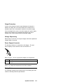
Attention
The term Reserved describes certain signals, bits, and registers that
should not be changed. Use of reserved areas can cause
compatibility problems, loss of data, or permanent damage to the
hardware. When the contents of a register are changed, the state of
the reserved bits must be preserved. Read the register first and
change only the bits that must be changed.
Copyright IBM Corp. 1997
ix
x
Preface
Section 1. System Overview
Description
. . . . . . . . . . . . . .
System Board Devices and Features
System Board I/O Address Map . .
Specifications . . . . . . . . . . . . .
Performance Specifications . . .
Physical Specifications . . . . . .
Electrical Specifications
. . . . .
Acoustical Readings
. . . . . . .
Power Supply . . . . . . . . . . . . .
Voltages . . . . . . . . . . . . . .
Output Protection . . . . . . . . .
Voltage Sequencing . . . . . . . .
Power Supply Connector . . . . .
Battery Pack
. . . . . . . . . . . . .
Copyright IBM Corp. 1997
. .
.
. .
. .
. .
. .
. .
. .
. .
. .
. .
. .
. .
. .
.
.
.
.
.
.
.
.
.
.
.
.
.
.
.
.
.
.
.
.
.
.
.
.
.
.
.
.
.
.
.
.
.
.
.
.
.
.
.
.
.
.
.
.
.
.
.
.
.
.
.
.
.
.
.
.
.
.
.
.
.
.
.
.
.
.
.
.
.
.
.
.
.
.
.
.
.
.
.
.
.
.
.
.
.
.
.
.
.
.
.
.
.
.
.
.
.
.
.
.
.
.
.
.
.
.
.
.
.
.
.
.
.
.
.
.
.
.
.
.
.
.
.
.
.
.
.
.
.
.
.
.
.
.
.
.
.
.
.
.
.
.
.
.
.
.
.
.
.
.
.
.
.
.
.
.
.
.
.
.
.
.
.
.
.
.
.
.
.
.
.
.
.
.
.
.
.
.
.
.
.
.
.
.
.
.
.
.
.
.
1-2
1-3
1-5
1-7
1-7
1-8
1-9
1-9
1-10
1-10
1-11
1-11
1-11
1-11
1-1
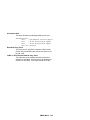
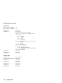
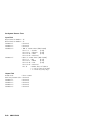
Description
The IBM ThinkPad 770 computer (hereafter called the ThinkPad
computer or the computer) is notebook-size computer that feature
the AT bus architecture. Each computer supports one UltraBay II
and one internal hard disk drive. The ThinkPad 770 computer also
supports an internal CD-ROM drive or an internal DVD drive as an
option.
Programs can distinguish the foregoing computer model from other
ThinkPad models by reading the system ID:
Interrupt 15H
Function code (AH)=23H and (AL)=10H.
Returns
(AL)=27H
The system microprocessor contains an internal cache and cache
controller.
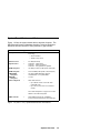
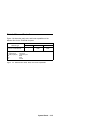
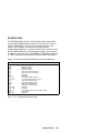
Figure 1-1 lists the model bytes, submodel bytes, and system clock
speed of the system board for each model.
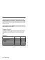
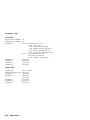
Model
Model Byte
(Hex)
Submodel Byte
(Hex)
System Clock
770
FC
01
33 MHz
Figure 1-1. Model and Submodel Bytes
For a listing of the other systems, refer to the IBM Personal
System/2 and Personal Computer BIOS Interface.
1-2
System Overview
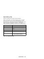
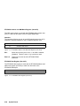
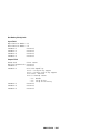
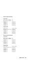
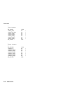
System Board Devices and Features
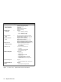
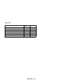
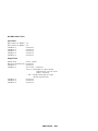
Figure 1-2 lists the system board devices and their features. The
IBM Personal System/2 Hardware Interface Technical Reference
describes devices common to PS/2 products by type number.
Device
Type
Features
Microprocessor
–
Intel Pentium processor with the MMX
technology
200 or 233 MHz
32 KB on-chip cache
External cache
–
512 KB (write back)
System timers
1
Channel 0: system timer
Channel 1: refresh generation
Channel 2: tone generator for speaker
ROM subsystem
–
128 KB by 4 banks (1 KB equals 1024 bytes)
RAM subsystem
–
32 to 256 MB (1 MB equals 1,048,576 bytes)
CMOS RAM
subsystem
–
128 bytes CMOS RAM with real-time
clock/calendar + 4 K byte NVRAM
EEPROM
subsystem
–
1 K bits
Video subsystem
–
XGA video functions:
Up to 65,536 colors on the TFT XGA
(1024x768) LCD
Up to 16,777,216 colors on an external
monitor
See “Video Subsystem” on page 3-2 for more
details on the video subsystem.
DMA controller
1
Seven DMA channels (AT compatible:)
Four 8-bit channels and three 16-bit channels
Figure 1-2 (Part 1 of 2). System Board Devices and Features
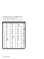
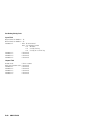
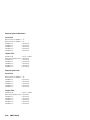
System Overview
1-3
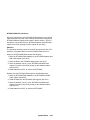
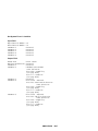
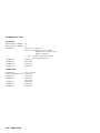
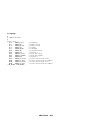
Device
Type
Features
Interrupt controller
1
Keyboard/auxiliary
device controller
1
Diskette drive
controller
2
15 levels of system interrupts
(interrupts are edge-triggered)
Internal keyboard
TrackPoint
Auxiliary device connector
Password security
Supports:
Serial controller
port
2
Parallel controller
port
1
Expansion bus
adapter (PCI-bus)
–
PCMCIA** slots
–
3.5-in. diskette (1.44 MB)
3.5-in. diskette (1.2 MB)
3.5-in. diskette (720 KB)
EIA-232-E interface (16550 compatible)
Programmable as serial port 1, 2, 3, or 4
One 9-pin, D-sub connector
Programmable as parallel port 1, 2, or 3
IEEE P1284-A compatible
Supports bidirectional input and output
Enhanced Parallel Port (EPP) compatible
Extended Capabilities Port (ECP) compatible
Supports externally attached devices:
SelectaDock docking system
Port replicator
Conforms to the standards for:
CardBus
Two Type I or II PC cards
One Type III PC card
Modem subsystem
–
Is driven by:
Infrared subsystem
–
MDSP 3780i
SRAM 32 Kb by 40 bits
Crystal Audio
Voice band CODEC for modem
Internal DAA
Internal omnidirectional microphone
Supports:
ThinkPad IR/SIR/D-ASK (500 KHz) IR
Universal serial bus
(USB)
–
Supports:
USB input and output devices
Figure 1-2 (Part 2 of 2). System Board Devices and Features
1-4
System Overview
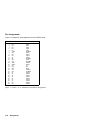
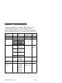
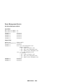
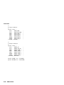
System Board I/O Address Map
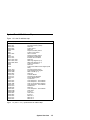
Figure 1-3 is the I/O address map.
Address (Hex)
Device
0000–001F
0020, 0021
0022–002F
0040–0043
0048–004B
0060
0061
0062, 0066
0064
0070, 0071
0072, 0073
0074, 0075, 0076
0081–0083, 0087
0089–008B, 008F
0092
0096
0098
DMA Controller (0–3)
Interrupt Controller (master)
Reserved
System Timer 1
Reserved
Keyboard, Auxiliary Device
System Control Port B
Slave Controller
Keyboard, Auxiliary Device
RT/CMOS and NMI Mask
Extended RT and CMOS
Reserved
DMA Page Registers (0–3)
DMA Page Registers (4–7)
System Control Port A
Reserved
System Flash ROM Control Register (DCR
2282)
Interrupt Controller (slave)
Power Management Register
DMA Controller (4–7)
Reserved
ThinkPad Modem
Secondary IDE Registers
Primary IDE Registers
Joystick Port
Audio Subsystem - Sound Blaster
Audio Subsystem - Sound Blaster
Super I/O Configuration Registers
Audio Subsystem - Sound Blaster
Parallel Port 3
Reserved
Audio Subsystem - Sound Blaster
Serial Port 4
IR Port 4
Serial Port 2
IR Port 2
MIDI Port 1
MIDI Port 2
MIDI Port 3
00A0, 00A1
00B2–00B3
00C0–00DF
00F0–00FF
0130–013F
0170–0177
01F0–01F7
0201
0220–0233
0240–0253
026E, 026F
0260–0273
0278–027A
027B–027F
0280–0283
02E8–02EF
02E8–02EF
02F8–02FF
02F8–02FF
0300–0303
0310–0313
0320–0323
Figure 1-3 (Part 1 of 2). System Board I/O Address Map
System Overview
1-5
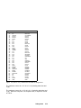
Address (Hex)
Device
0330–0333
0350–035F
0376, 0377
0378–037A
037B–037F
0388–038B
0398–0399
03B4, 03B5, 03BA
03BC–03BE
03C0–03C5
03C6–03C9
03CA, 03CC, 03CE, 03CF,
03D4, 03D5, 03DA,
03D8–03DA
03E0–03E1
03E8–03EF
03E8–03EF
03F0–03F5, 03F7
03F6, 03F7
03F8–03FF
03F8–03FF
0530–0537
0538–053F
0604–060B
0770–077F
0CF8–0CFB
0CFC–0CFF
0DB0–0DBF
0D38–0D3F
0E80–0E87
0E88–0E8F
0F40–0F47
0FF0–0FF7
15E8–15EF
2120–21FF
23C0–23C7
46E8
EF00–EF37
EFA0–EFAD
F104
MIDI Port 4
ThinkPad Modem
Secondary IDE Registers
Parallel Port 2
Reserved
Audio Subsystem - FM Synthesizer
Reserved
Video Subsystem
Parallel Port 1
Video Subsystem
Video DAC
Video Subsystem
PCMCIA Interface (DCR 2959)
Serial Port 3
IR Port 3
Diskette-Drive Controller
Primary IDE Registers
Serial Port 1
IR Port 1
Audio - WSS 1
Audio Control Port 1
Audio - WSS 2
ThinkPad Modem
PCI Configuration Address Register
PCI Configuration Data Register
ThinkPad Modem
Audio Control Port 2
Audio - WSS 3
Audio Control Port 3
Audio - WSS 4
Audio Control Port 4
Power Management Register
Reserved
Reserved
Video Subsystem Enable
Power Management Register
SMBus IO Space Register
Reserved
Figure 1-3 (Part 2 of 2). System Board I/O Address Map
1-6
System Overview
Specifications
Figure 1-4 to Figure 1-7 on page 1-9 list the specifications for the
computers.
Performance Specifications
Device/Cycle
Microprocessor
L1 cache (64bit)
read/write hit
L2 cache (64bit) (for not all
models)
read hit (back-to-back)
write hit (back-to-back)
Memory (64bit) (see Note)
read, page hit
read, raw miss
read, page miss
posted write
write retire rate from
write buffer
Clock Counts
(66 MHz)
200 or 233
MHz
1 CPUCLK
90 ns (60 ns)
90 ns (60 ns)
240 ns
285 ns
345 ns
90 ns
135 ns
Note:
The cycle times shown for access to system
board RAM are based on 70 ns EDO memory.
Figure 1-4. Performance Specifications
System Overview
1-7
Physical Specifications
Size
Width: 313.0 mm (12.3 in.)
Depth: 240.0 / 254.0 mm (9.45 / 10.00 in.)
Height: 56.0 mm (2.20 in.)
Weightñ (approximate value)
3.4 kg (7.4 lb)
3.5 kg (7.7 lb)
Air Temperature
System on (without diskette)
5.0°C to 35.0°C (41°F to 95°F)
System on (with diskette)
10.0°C to 35.0°C (50°F to 95°F)
System off
5.0°C to 43.0°C (41°F to 110°F)
Humidity
System (without diskette)
8% to 95%
System (with diskette)
8% to 80%
Maximum altitudeò: 3,048 m (10,000 ft) in unpressurized conditions
Heat output: 56 W
Acoustical readings (see Figure 1-7 on page 1-9)
Electrical (see Figure 1-6 on page 1-9)
Electromagnetic compatibility: FCC class B
ñ With battery pack installed.
ò This is the maximum altitude at which the specified air temperatures apply. At
higher altitudes, the maximum air temperatures are lower than those specified.
Figure 1-5. Physical Specifications
1-8
System Overview
Electrical Specifications
(56 W)
Input voltageñ
(V ac)
100–240
Frequency (Hz)
50/60
Inputò (kVA)
0.13
ñ Range is automatically selected; sine wave input is required.
ò At maximum configuration.
Figure 1-6. Electrical Specifications
Acoustical Readings
LWAd in bels
<LpA>m in dB
LpAm in dB
Operate
Idle
Operate
Idle
Operate
Idle
770
4.40
3.90
35.0
30.0
30.0
25.5
770 (with
SelectaDock
III)
4.60
4.30
37.5
34.0
31.0
28.0
Notes:
LWAd
Is the declared sound power level for the random sample of
machines.
LpAm
Is the mean value of the A-weighted sound pressure levels at the
operator position (if any) for the random sample of machines.
<LpA>m
Is the mean value of the A-weighted sound pressure levels at the
1 meter position for the random sample of machines.
Operate
Shows the value while using the hard disk drive.
All measurements made in accordance with ANSI S12.10 and reported in
conformance with ISO 9296.
Figure 1-7. Acoustical Readings
System Overview
1-9
Power Supply
The power supply converts the ac voltage to dc voltage and provides
power for the following:
System board set
Diskette drive
Hard disk drive
CD-ROM drive
Auxiliary devices
Keyboard
LCD panel
PCMCIA cards
DVD drive
Voltages
The power supply generates six different dc voltages: VCC5M,
VCC3M, VCC12, and VCCSW. Figure 1-8 shows the maximum
current for each voltage.
Output
Voltage (V dc)
Current (A)
VCC5M
+5.0
5.80
VCC3M
+3.3
6.00
VCC12
+12.0
0.50
VCCSW
+5.0
0.01
Figure 1-8. Power Supply Maximum Current
1-10
System Overview
Output Protection
A short circuit placed on any dc output (between two outputs or
between an output and a dc return) latches all dc outputs into a
shutdown state, with no hazardous condition to the power supply.
If an overvoltage fault occurs in the power supply, the power supply
latches all dc outputs into a shutdown state before any output
exceeds 135% of the nominal value of the power supply.
Voltage Sequencing
When power is turned on, the output voltages reach their operational
voltages within 2 seconds.
Power Supply Connector
The following connector is used with the AC adapter. The total
power capacity of this connector must not exceed 4.0 A.
Refer to Figure 1-9 for the appropriate adapter pin assignments.
Pin
Voltage
1
2
+7.0 V dc to +17.0 V dc (depending on charging conditions)
Ground
Figure 1-9. Voltage Pin Assignments for the 56W AC Adapter
Battery Pack
The ThinkPad computer uses a lithium-ion (Li-ion) battery pack that
meets the following electrical specifications:
System Overview
1-11
Nominal Voltage
+10.8 V dc
Capacity (average)
4.5 ampere hours (AH)
Protection
Overcurrent protection
Overvoltage protection
Overdischarge protection
Thermal protection
Figure 1-10. Lithium-ion Battery Pack Specifications
1-12
System Overview
Section 2. System Board
Description
. . . . . . . . . . . . . . . . . . . . . . . . . . . .
Microprocessor . . . . . . . . . . . . . . . . . . . . . . . . . .
Cache Memory Operation . . . . . . . . . . . . . . . . . .
Cacheable Address Space . . . . . . . . . . . . . . . . . .
Bus Adapter . . . . . . . . . . . . . . . . . . . . . . . . . . . .
Keyboard/Mouse Connector . . . . . . . . . . . . . . . . . . .
Signals . . . . . . . . . . . . . . . . . . . . . . . . . . . . .
Connector
. . . . . . . . . . . . . . . . . . . . . . . . . . .
Scan Codes . . . . . . . . . . . . . . . . . . . . . . . . . .
Keyboard ID . . . . . . . . . . . . . . . . . . . . . . . . . .
Displayable Characters and Symbols . . . . . . . . . . . .
Hard Disk Drive Connector . . . . . . . . . . . . . . . . . . .
External Bus Connector . . . . . . . . . . . . . . . . . . . . .
UltraBay II Connector . . . . . . . . . . . . . . . . . . . . . .
Diskette Drive and Controller . . . . . . . . . . . . . . . . . .
Memory . . . . . . . . . . . . . . . . . . . . . . . . . . . . . .
ROM Subsystem
. . . . . . . . . . . . . . . . . . . . . . .
RAM Subsystem . . . . . . . . . . . . . . . . . . . . . . . .
System Memory Map . . . . . . . . . . . . . . . . . . . . .
. . . .
System Board Memory for the DIMM Connectors
RT/CMOS RAM . . . . . . . . . . . . . . . . . . . . . . . .
RT/CMOS Address and NMI Mask Register (Hex 0070)
RT/CMOS Data Register (Hex 0071) . . . . . . . . . .
RT/CMOS RAM I/O Operations . . . . . . . . . . . . .
CMOS RAM Configuration . . . . . . . . . . . . . . . .
Miscellaneous System Functions and Ports
. . . . . . . . .
Nonmaskable Interrupt (NMI) . . . . . . . . . . . . . . . .
System Control Port A (Hex 0092) . . . . . . . . . . . . .
System Control Port B (Hex 0061) . . . . . . . . . . . . .
Power-On Password . . . . . . . . . . . . . . . . . . . . .
Other Passwords . . . . . . . . . . . . . . . . . . . . . . .
Selectable Drive-Startup Sequence . . . . . . . . . . . . .
Hardware Compatibility . . . . . . . . . . . . . . . . . . . . .
Error Codes . . . . . . . . . . . . . . . . . . . . . . . . . . . .
Copyright IBM Corp. 1997
.
.
.
.
.
.
.
.
.
.
.
.
.
.
.
.
.
.
.
.
.
.
.
.
.
.
.
.
.
.
.
.
.
.
.
.
.
.
.
.
.
.
.
.
.
.
2-2
2-2
2-2
2-3
2-3
2-4
2-4
2-4
2-5
2-6
2-7
2-8
2-9
2-12
2-15
2-16
2-16
2-16
2-17
2-18
2-19
2-20
2-20
2-21
2-25
2-29
2-29
2-30
2-31
2-32
2-32
2-33
2-34
2-35
2-1
Description
This section describes the microprocessor, connectors, memory
subsystems, and miscellaneous system functions and ports for the
ThinkPad computers.
Microprocessor
The ThinkPad 770 uses the Intel Pentium 200 or 233 MHz
processor with the MMX technology.
The Processor has a 32-bit address bus and a 64-bit data bus. It is
software-compatible with all previous microprocessors. The
Processor has an internal, split data and instruction, 32KB write-back
cache. It includes pipelined math coprocessor functions and
superscalar architecture (two execution units).
Cache Memory Operation
In addition to the 32 KB of internal Level 1 (L1) cache memory in the
microprocessor, the system board of the ThinkPad 770 computer
contains an additional 256 KB of external Level 2 (L2) cache
memory.
The cache memory in the Intel Pentium microprocessor and the L2
external cache memory enable the microprocessor to read
instructions and data much faster than if the microprocessor had to
access system memory. When an instruction is first used or data is
first read or written, it is transferred to the cache memory from main
memory. This enables future accesses to the instructions or data to
occur much faster.
The cache is disabled and empty when the microprocessor comes
out of the reset state. The cache is tested and enabled during the
power-on self-test (POST).
The cache memory in the Intel Pentium microprocessor is loaded
from system memory in 32-byte increments, each referred to as a
cache line. A cache line is aligned on a paragraph boundary. A
reference to any byte contained in a cache line results in the entire
line being read into the cache memory (if the data was not already in
the cache). When the microprocessor gives up control of the system
bus, the cache memory enters “snoop” mode and monitors all write
2-2
System Board
and read operations. If memory data is written to a location in the
cache and the cache line is in the “modified” state, the corresponding
cache line is written back to system memory and invalidated.
When the microprocessor performs a memory read, the data address
is used to find the data in the cache. If the data is found (a hit), it is
read from the cache memory and no external bus cycle occurs. If
the data is not found (a miss), an external bus cycle is used to read
the data from system memory. If the address of the missed data is
in cacheable address space, the data is stored in the cache memory
and the remainder of the cache line is read.
When the microprocessor performs a memory write, the data
address is used to search the cache. If the address is found (hit),
the data is written to the cache and no external bus cycle is used to
write the data to system memory. (If the address of the write
operation was not in the cache memory but was in cacheable
address space, the data is read back into the cache memory and the
remainder of the cache line is read.)
Cacheable Address Space
Cacheable address space is defined as system memory that resides
on the system board (0–640 KB and 1 MB–256 MB). Cacheability of
system memory is up to 64 MB in the L2 cache. Nothing in address
range hex A0000–BFFFF, I/O address space, or memory in any AT
slot is cached.
ROM address space (hex C0000–C9FFF and F0000–FFFFF) is L1
cacheable for code read operations only. If data in this address
range is already in cache memory and the address range is written
to, the cached line is invalidated and is read again from RAM, where
the BIOS is shadowed.
Bus Adapter
When the computer is attached to the ThinkPad SelectaDock III
docking system, the PCI adapters or AT-bus adapters can be used
through the docking system.
System Board
2-3
Keyboard/Mouse Connector
Each ThinkPad computer has a keyboard/mouse connector, where
the IBM mouse, keyboard, or numeric keypad is connected.
Signals
The keyboard and mouse signals are driven by open-collector drivers
pulled to 5 V dc through a pull-up resistor. Figure 2-1 lists the
signals.
Sink current
High-level output voltage
Low-level output voltage
High-level input voltage
Low-level input voltage
1 mA
5.0 V
0.5 V
2.0 V
0.8 V
dc minus pullup
dc
dc
dc
Maximum
Minimum
Maximum
Minimum
Maximum
Figure 2-1. Keyboard and Mouse Signals
Connector
The keyboard/mouse connector uses a 6-pin, miniature DIN
connector.
6
5
4
3
2
1
Pin
I/O
Signal Name
1
2
3
4
5
6
I/O
I/O
–
–
I/O
I/O
Mouse Data
Keyboard Data
Ground
+5 V dc
Mouse Clock
Keyboard Clock
Figure 2-2. Keyboard/Mouse Connector Pin Assignments
Note: The maximum current for +5 V dc (pin 4) is 0.5 A for both the
mouse and the numeric keypad.
2-4
System Board
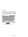
Scan Codes
Figure 2-3 shows the key numbers assigned to keys on the 84-key
keyboard (for the U.S. and Japan). Figure 2-4 on page 2-6 shows
the key numbers assigned to keys on the 85-key keyboard (for
countries other than the U.S. and Japan). For scan codes assigned
to each numbered key, refer to the IBM Personal System/2 Hardware
Interface Technical Reference.
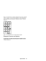
Figure 2-3. Key Numbers for the 84-Key Keyboard
System Board
2-5
Figure 2-4. Key Numbers for the 85-Key Keyboard
Keyboard ID
The keyboard ID consists of 2 bytes: hex 83AB (the built-in keyboard
with the external numeric keypad) or hex 84AB (the built-in keyboard
only). Interrupt 16H, function code (AH)=0AH, returns the keyboard
ID.
2-6
System Board
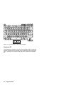
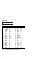
Figure 2-5 shows the key numbers assigned to keys on the external
numeric keypad. For scan codes assigned to each numbered key,
refer to the IBM Personal System/2 Hardware Interface Technical
Reference.
90
95
100
91
96
101
92
97
102
93
98
103
105
106
108
99
104
Figure 2-5. Key Numbers for the External Numeric Keypad
Displayable Characters and Symbols
For displayable characters and symbols that are keyable from the
keyboard, refer to the IBM Personal System/2 Hardware Interface
Technical Reference.
System Board
2-7
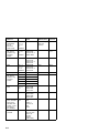
Hard Disk Drive Connector
The hard disk drive connected to the system board is removable.
Figure 2-6 shows the pin assignments for the connector on the
system board.
Pin
1
2
3
4
5
6
7
8
9
10
11
12
13
14
15
16
17
18
19
20
21
22
23
24
25
26
27
28
29
30
Signal
I/O or Feature
DetectIn
Jumper A
Jumper B
Jumper C
Jumper D
RSTDRV
GND
PDD7
PDD8
GND
PDD6
PDD9
GND
PDD5
PDD10
GND
PDD4
PDD11
GND
PDD3
PDD12
GND
PDD2
PDD13
GND
PDD1
PDD14
GND
PDD0
PDD15
O
NC
O
O
O
O
Ground
I/O
I/O
Ground
I/O
I/O
Ground
I/O
I/O
Ground
I/O
I/O
Ground
I/O
I/O
Ground
I/O
I/O
Ground
I/O
I/O
Ground
I/O
I/O
Pin
31
32
33
34
35
36
37
38
39
40
41
42
43
44
45
46
47
48
49
50
51
52
53
54
55
56
57
58
59
60
Signal
Figure 2-6. Hard Disk Drive Connector Pin Assignments
2-8
System Board
I/O or Feature
GND
Ground
NC
NC
-PDREQ
I
GND
Ground
-PDIOW
O
GND
Ground
-PDIOR
O
GND
Ground
PIORDY
I
CSEL
O
-PDACK
O
GND
Ground
IRQ14HDD I
-IOCS16
I
PDA1
O
-PDIAGHDD O
GND
Ground
PDA0
O
PDA2
O
-CS1P
O
-CS3P
O
-DASPHDD I
GND
Ground
VCC5B
Vcc
VCC5B
Vcc
VCC5B
Vcc
VCC5B
Vcc
Reserved
NC
-HDDDETECTI
GND
Ground
External Bus Connector
The docking station is connected through the 240-pin external bus
connector on the rear panel. This connector is installed on the
system board and has the following pin assignments:
60
121 1
240
120
180
61 181
Type Legend:
A: Audio signal
C: System control signal
F: Diskette drive signal
G: Ground
I: IDE hard disk drive signal
J: Joy stick / Midi
K: Keyboard/mouse signal
L: Parallel port
M: PC Card signal
P: PCI-bus signal
R: Reserved
S: Serial port signal
T: ISA-bus signal
U: USB
V: Video signal
W: Power line
System Board
2-9
Pin
001
002
003
004
005
006
007
008
009
010
011
012
013
014
015
016
017
018
019
020
021
022
023
024
025
026
027
028
029
030
031
032
033
034
035
036
037
038
039
040
041
042
043
044
045
046
047
048
049
050
051
052
053
054
055
056
057
058
059
060
2-10
Type
W
W
P
G
P
P
G
P
P
G
P
P
G
P
P
G
P
P
G
P
P
G
P
R
G
P
P
R
R
R
R
P
P
G
P
P
G
P
P
G
P
P
G
P
R
G
S
S
S
S
W
K
G
A
A
A
W
W
W
W
Signal Name
VCC5A
VCC5A
-PCIRST
GND
-ACK_GNT
-CLKRUN
GND
AD30
AD28
GND
AD26
AD24
GND
AD23
AD21
GND
AD19
AD17
GND
CBE2
-IRDY
GND
-DEVSEL
Reserved
GND
-SERR
PAR
Reserved
Reserved
Reserved
Reserved
AD14
AD12
GND
AD10
AD8
GND
AD7
AD5
GND
AD3
AD1
GND
PRDY
Reserved
GND
-DCD
TXD
-RTS
-DSR
KBD_+5V
KBCLK
GND
R_IN
AGND
R_OUT
Dock-POR
Dock-POR
Dock-POR
Dock-POR
System Board
Pin
061
062
063
064
065
066
067
068
069
070
071
072
073
074
075
076
077
078
079
080
081
082
083
084
085
086
087
088
089
090
091
092
093
094
095
096
097
098
099
100
101
102
103
104
105
106
107
108
109
110
111
112
113
114
115
116
117
118
119
120
Type
W
W
W
W
A
A
A
G
K
K
K
G
S
S
S
S
G
P
P
G
P
P
G
P
P
G
P
P
R
R
R
R
P
P
G
P
P
G
P
P
G
P
P
G
P
P
G
P
P
G
P
P
G
P
P
G
P
C
W
W
Signal Name
Dock-PWR
Dock-PWR
Dock-PWR
Dock-PWR
L_OUT
AGND
L_IN
GND
KBDATA
MSDATA
MSCLK
GND
-RI
-CTS
-DTR
RXD
GND
AD0
AD2
GND
AD4
AD6
GND
CBE0
AD9
GND
AD11
AD13
R/-S
Reserved
Reserved
Reserved
AD15
CBE1
GND
-PERR
-STOP
GND
-TRDY
-FRAME
GND
AD16
AD18
GND
AD20
AD22
GND
CBE3
AD25
GND
AD27
AD29
GND
AD31
-REQ
GND
PCICLK
-BATOPDSBL
VCC5B
VCC5B
Pin
121
122
123
124
125
126
127
128
129
130
131
132
133
134
135
136
137
138
139
140
141
142
143
144
145
146
147
148
149
150
151
152
153
154
155
156
157
158
159
160
161
162
163
164
165
166
167
168
169
170
171
172
173
174
175
176
177
178
179
180
Type
C
P
G
T
T
T
T
T
G
P
P
P
I
G
V
V
V
V
G
L
L
L
L
G
L
L
L
L
L
G
G
L
F
G
F
F
F
F
G
F
F
F
F
G
C
C
C
M
G
J
J
J
J
G
C
C
R
U
G
C
Signal Name
-DOCK_ID1
IRQSER
GND
IRQ5
IRQ7
IRQ10
IRQ11
IRQ14
GND
-INTB
-INTC
-INTD
-DASP
GND
CRTID0
CDTID2
DDCCLK_ID3
CRT_RED
GND
SLCT
PE
BUSY
D7
GND
D3
D2
D1
D0
AFD
GND
GND
-ERR
-WRDATA
GND
DRVSEL1
-DRVID0
-MEDID0
DRATE1
GND
-STEP
-MEDID1
-TRACK0
-WPROTECT
GND
-PWRON
POWERGOOD
UNI_SMI
SPKR
GND
JAB1
JAB2
JACX
JACY
GND
I2C_CLK
SUSCLK
Reserved
USB_OC1
GND
-DOCK_ID3
Pin
181
182
183
184
185
186
187
188
189
190
191
192
193
194
195
196
197
198
199
200
201
202
203
204
205
206
207
208
209
210
211
212
213
214
215
216
217
218
219
220
221
222
223
224
225
226
227
228
229
230
231
232
233
234
235
236
237
238
239
240
Type
C
G
U
U
R
G
C
J
J
J
G
J
J
J
C
G
C
M
F
G
F
F
F
F
G
F
F
F
F
G
G
L
L
L
G
L
L
L
L
G
V
G
V
V
V
V
G
I
I
G
P
I
T
T
T
T
T
T
G
C
Signal Name
-DOCK_ID2
GND
USBP1UDBP1+
Reserved
GND
12C_DATA
JBCY
JBCX
JBB2
GND
JBB1
MIDIOUT
MIDIIN
-PWRSWITCH
GND
-BUSSUSSTAT
-PCMCIA_RI
-SIDE1SEL
GND
DRATE0
-WREN
-DRVID1
-DIR
GND
-MOTEN1
-DISKCHG
-INDEX
-RDDATA
GND
GND
-STB
-INIT
-SLIN
GND
D4
D5
D6
-ACK
GND
CRT_GREEN
GND
CRT_BLUE
DDCDATA_ID1
VSYNC
HSYNC
GND
-PHLDA
-PHLD
GND
-INTA
IDE2IRQ
IRQ15
IRQ12
IRQ9
IRQ6
IRQ4
IRQ3
GND
-DOCK_ID0
Figure 2-7. 240-Pin External Bus Connector Pin Assignments
System Board
2-11
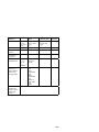
UltraBay II Connector
The removable diskette drive, secondary hard disk drive, DVD drive,
or CD-ROM drive can be connected to the UltraBay II connector on
the system board. This connector has the following pin assignments.
2-12
System Board
Pin
1
2
3
4
5
6
7
8
9
10
11
12
13
14
15
16
17
18
19
20
21
22
23
24
25
26
27
28
29
30
31
32
33
34
35
36
37
38
39
40
41
42
43
44
45
46
47
48
49
50
Signal
I/O and Feature
UBAYID1
UBAYID2
GND
GND
-INDEX
-DRVSEL0
-DISKCHG
-DRVID0
NC
-MEDID0
-MONTEN0
DRATE1
-DIR
-DRVID1
-STEP
GND
-WRDATA
GND
-WREN
-MEDID1
-TRACK0
DRATE0
-WPROTECT
-RDDATA
GND
-SIDE1SEL
UBAYID0
RSTDRV
GND
DD7
DD8
DD6
DD9
GND
DD5
DD10
DD4
DD11
VCC5B
VCC5B
VCC5B
VCC5B
DD3
DD12
DD2
DD13
GND
DD1
DD14
DD0
I
I
GND
GND
I
O
I
I
N/C
I
O
O
O
I
0
GND
O
GND
O
I
I
O
I
I
GND
O
O
O
GND
I/O
I/O
I/O
I/O
GND
I/O
I/O
I/O
I/O
VCC
VCC
VCC
VCC
I/O
I/O
I/O
I/O
GND
I/O
I/O
I/O
Figure 2-8 (Part 1 of 2). UltraBay II Connector Pin Assignments
System Board
2-13
Pin
51
52
53
54
55
56
57
58
59
60
61
62
63
64
65
66
67
68
69
70
71
72
73
74
75
76
77
78
79
80
Signal
I/O and Feature
DD15
GND
-UBAY_HDD
DMARQ
GND
-DIOW
GND
-DIOR
GND
IORDY
CSEL
-DMACK
IRQ
-IOCS16
DA1
-PDIAG
DA0
DA2
-CS1
-CS3
-DASP
-MCS
CD_MUTE
AUDIO_RTN
CD_L_IN
CD_R_IN
GND
GND
UBAYID3
UBAYID4
I/O
GND
I
I
GND
O
GND
O
GND
I
O
O
I
I
O
I/O
O
O
O
O
I
O
I
I
I
I
GND
GND
I
I
Figure 2-8 (Part 2 of 2). UltraBay II Connector Pin Assignments
2-14
System Board
Diskette Drive and Controller
Figure 2-9 shows the read, write, and format capabilities of the
diskette drive for the ThinkPad computer.
Format Size
Diskette Type
3.5-inch 1.0 MB Diskette
3.5-inch 2.0 MB Diskette
720 KB
1.2 MB
1.44 MB
RWF
−
−
RWF
−
RWF
Legend::
1 KB (kilobyte)
1 MB (megabyte)
R
W
F
1024 bytes
1,048,576 bytes
Read
Write
Format
Figure 2-9. Diskette Drive Read, Write, and Format Capabilities
System Board
2-15
Memory
The ThinkPad computers use the following types of memory:
Read-only memory (ROM)
Random access memory (RAM)
Real-time clock/complementary metal-oxide semiconductor RAM
(RT/CMOS RAM)
ROM Subsystem
The ROM subsystem consists of four banks of 128 KB memory.
ROM is active when power is turned on and is assigned to the top of
the first and last 1 MB of address space (hex 000F0000–000FFFFF
and hex FFFF0000–FFFFFFFF). After POST checks that system
memory is operating correctly, the ROM code is copied to RAM at
the same address space, and ROM is disabled.
RAM Subsystem
The RAM subsystem on the system board starts at address
hex 00000000 of the address space. The RAM subsystem for the
ThinkPad 770 is 64 bits wide.
The 32 MB base memory is on the system board. Two 144-pin
8-byte dual inline memory module (DIMM) connectors are provided
on the system board. Both connectors accept an 8 MB, a 16 MB, a
32 MB, a 64 MB, or a 128 MB DIMM. The memory capacity can be
increased up to 256 MB. When two 128 MB DIMMs are installed,
the base 32 MB memory on the system board becomes inoperative.
The total amount of usable memory is less than the amount of
memory installed because of ROM-to-RAM remapping and power
management.
2-16
System Board
System Memory Map
Memory is mapped by the memory controller registers.
Figure 2-10 on page 2-17 shows the memory map for a correctly
functioning system. Memory can be mapped differently if POST
detects an error in system board memory or RT/CMOS RAM. In the
figure, the variable x represents the number of 1 MB blocks of
system board memory starting at or above the hex 100000 boundary.
Hex Address Range
Function
00000000 to 0009FFFF
640 KB system board RAM
000A0000 to 000BFFFF
Video RAM
000C0000 to 000C9FFF
System board video BIOS ROM mapped to
RAM
000C8000 to 000EFFFF
Channel ROM
000F0000 to 000FFFFF
64 KB system board ROM mapped to RAM
00100000 to (00100000 + x
MB)
x MB system board RAM
FFFF0000 to FFFFFFFF
64 KB system board ROM
(same as 000F0000 to 000FFFFF)
Figure 2-10. System Memory Map
System Board
2-17
System Board Memory for the DIMM Connectors
The system board has two DIMM connectors.
Figure 2-11 shows the pin assignments for the DIMM connector.
Pin
Signal
Pin
1
2
3
4
5
6
7
8
9
10
11
12
13
14
15
16
17
18
19
20
21
22
23
24
25
26
27
28
29
30
31
32
33
34
35
36
37
Vss
Vss
DQ0
DQ32
DQ1
DQ33
DQ2
DQ34
DQ3
DQ35
Vcc
Vcc
DQ4
DQ36
DQ5
DQ37
DQ6
DQ38
DQ7
D39
Vss
Vss
DQMB0
DQMB4
DQMB1
DQMB5
Vcc
Vcc
A0
A3
A1
A4
A2
A5
Vss
Vss
DQ8
38
39
40
41
42
43
44
45
46
47
48
49
50
51
52
53
54
55
56
57
58
59
60
61
62
63
64
65
66
67
68
69
70
71
72
73
74
Signal
Pin
Signal
Pin
Signal
D40
DQ9
DQ41
DQ10
DQ42
DQ11
DQ43
Vcc
Vcc
DQ12
DQ44
DQ13
DQ45
DQ14
DQ46
DQ15
DQ47
Vss
Vss
Reserved
Reserved
Reserved
Reserved
CK
CKE
Vcc
Vcc
/RAS
/CAS
/WE
RFU
/S0
RFU
/S1
RFU
RFU
RFU
75
76
77
78
79
80
81
82
83
84
85
86
87
88
89
90
91
92
93
94
95
96
97
98
99
100
101
102
103
104
105
106
Vss
Vss
Reserved
Reserved
Reserved
Reserved
Vcc
Vcc
DQ16
DQ48
DQ17
DQ49
DQ18
DQ50
DQ19
DQ51
Vss
Vss
DQ20
DQ52
DQ21
DQ53
DQ22
DQ54
DQ23
DQ55
Vcc
Vcc
A6
A7
A8
A11
(BS0)
Vss
Vss
A9
110
A12
(BS1)
A10
(AP)
A13
Vcc
Vcc
DQMB2
DQMB6
DQMB3
DQMB7
Vss
Vss
DQ24
DQ56
DQ25
DQ57
DQ26
DQ58
DQ27
DQ59
Vcc
Vcc
DQ28
DQ60
DQ29
DQ61
DQ30
DQ62
DQ31
DQ63
Vss
Vss
SDA
SCL
Vcc
Vcc
107
108
109
111
112
113
114
115
116
117
118
119
120
121
122
123
124
125
126
127
128
129
130
131
132
133
134
135
136
137
138
139
140
141
142
143
144
Figure 2-11. DIMM Adapter Card Memory Connector Pin Assignments
2-18
System Board
RT/CMOS RAM
The RT/CMOS RAM (real-time clock/complementary metal-oxide
semiconductor RAM) module contains the real-time clock and 128
bytes of CMOS RAM. The clock circuitry uses 14 bytes of this
memory; the remainder is allocated to configuration and
system-status information. A battery is built into the module to keep
the RT/CMOS RAM active when the power supply is not turned on.
In addition to the 128 bytes of CMOS/RAM, a CMOS/RAM extension
of 4 KB is provided for configuration and other system information.
Figure 2-12 lists the RT/CMOS RAM bytes and their addresses.
Address (Hex)
RT/CMOS RAM Bytes
000–00D
00E
00F
010
011
012
013
014
015, 016
017, 018
019
01A
01B
01C
01D–02D
02E, 02F
030, 031
032
033–07F
Real-time clock
Diagnostic status
Shutdown status
Diskette drive type
Hard disk 2 and 3 drive type
Hard disk 0 and 1 drive type
Reserved
Equipment
Low and high base memory
Low and high expansion memory
Hard disk 0 extended byte
Hard disk 1 extended byte
Hard disk 2 extended byte
Hard disk 3 extended byte
Reserved
Checksum
Low and high usable memory above 1 MB
Date-century
Reserved
Figure 2-12. RT/CMOS RAM Address Map
System Board
2-19
RT/CMOS Address and NMI Mask Register (Hex 0070)
The NMI mask register is used with the RT/CMOS data register (hex
0071) to read from and write to the RT/CMOS RAM bytes.
Attention
The operation following a write to hex 0070 should access hex 0071;
otherwise, intermittent failures of the RT/CMOS RAM can occur.
Bit
Function
7
6–0
NMI mask
RT/CMOS RAM address
Figure 2-13. RT/CMOS Address and NMI Mask Register (Hex 0070)
Bit 7
When this write-only bit is set to 1, the NMI is masked
(disabled). This bit is set to 1 by a power-on reset.
Bits 6–0
These bits are used to select RT/CMOS RAM
addresses.
RT/CMOS Data Register (Hex 0071)
The RT/CMOS data register is used with the RT/CMOS address and
NMI mask register (hex 0070) to read from and write to the
RT/CMOS RAM bytes.
Bit
Function
7–0
RT/CMOS data
Figure 2-14. RT/CMOS Data Register (Hex 0071)
2-20
System Board
RT/CMOS RAM I/O Operations
During I/O operations to the RT/CMOS RAM addresses, you should
mask interrupts to prevent other interrupt routines from changing the
RT/CMOS address register before data is read or written. After I/O
operations, you should leave the RT/CMOS address and NMI mask
register (hex 0070) pointing to status register D (hex 00D).
Attention
The operation following a write to hex 0070 should access hex 0071;
otherwise, intermittent failures of the RT/CMOS RAM can occur.
Writing to the RT/CMOS RAM requires the following:
1. Write the RT/CMOS RAM address to the RT/CMOS address and
NMI mask register (hex 0070).
2. Write the data to the RT/CMOS data register (hex 0071).
3. Write the address, hex 0F, to the RT/CMOS and NMI mask
register; this leaves hex 0070 pointing to the shutdown status
byte (hex 0F).
4. Read address hex 0071 to restore the RT/CMOS.
Reading from the RT/CMOS RAM requires the following steps:
1. Write the RT/CMOS RAM address to the RT/CMOS and NMI
mask register (hex 0070).
2. Read the data from the RT/CMOS data register (hex 0071).
3. Write the address, hex 0F, to the RT/CMOS and NMI mask
register; this leaves hex 0070 pointing to the shutdown status
byte (hex 0F).
4. Read address hex 0071 to restore the RT/CMOS.
System Board
2-21
Real-Time Clock Bytes (Hex 000–00D): Bit definitions and
addresses for the real-time clock bytes are shown in Figure 2-15.
Address
(Hex)
Function
000
001
002
003
004
005
006
007
008
009
00A
00B
00C
00D
Seconds
Second alarm
Minutes
Minute alarm
Hours
Hour alarm
Day of week
Date of month
Month
Year
Status register
Status register
Status register
Status register
Byte Number
A
B
C
D
0
1
2
3
4
5
6
7
8
9
10
11
12
13
Figure 2-15. Real-Time Clock Bytes (Hex 000–00D)
Note: The setup program initializes status registers A and B when
the time and date are set. Interrupt 1AH is the BIOS
interface to read and set the time and date; it initializes the
registers in the same way that the setup program does.
Status Register A (Hex 00A)
Bit
Function
7
6
Update in progress (UIP)
Countdown chain
1 - resets countdown chain
0 - countdown chain enabled
Oscillator enable
0 - oscillator off
1 - oscillator on
Bank select
Rate-selection bits
5
4
3–0
Figure 2-16. Status Register A (Hex 00A)
Bit 7
2-22
This bit is a status flag that can be monitored. If this bit
is 1, the update transfer will soon occur. If this bit 0, the
update transfer will not occur for at least 244 µs.
System Board
Bits 6–5
If these bits are a pattern of 01, the oscillator is turned
on and the RTC is allowed to keep time. The next
update will occur at 500 ms after a pattern of 01 is
written to these bits.
Bits 4
To use the original bank of memory, select 0. To use
the extended registers, select 1.
Bits 3–0
These bits allow the selection of a divider output
frequency or disable the divider output.
Status Register B (Hex 00B)
Bit
Function
7
6
5
4
3
2
1
0
Set
Enable periodic interrupt
Enable alarm interrupt
Enable update-ended interrupt
Enable square wave
Date mode
24-hour mode
Enable daylight-saving time
Figure 2-17. Status Register B (Hex 00B)
Bit 7
If set to 0, this bit updates the cycle, normally by
advancing the count at a rate of one cycle per second. If
set to 1, it immediately ends any update cycle in
progress, and the program can initialize the 14 time bytes
without any further updates occurring until this bit is set
to 0.
Bit 6
This is a read/write bit that allows an interrupt to occur at
a rate specified by the rate and divider bits in status
register A. If set to 1, this bit enables the interrupt. The
system initializes this bit to 0.
Bit 5
If set to 1, this bit enables the alarm interrupt. The
system initializes this bit to 0.
Bit 4
If set to 1, this bit enables the update-ended interrupt.
The system initializes this bit to 0.
Bit 3
If set to 1, this bit enables the square-wave frequency as
set by the rate-selection bits in status register A. The
system initializes this bit to 0.
System Board
2-23
Bit 2
This bit indicates whether the binary-coded-decimal (BCD)
or binary format is used for time-and-date calendar
updates. If set to 1, this bit indicates binary format. The
system initializes this bit to 0.
Bit 1
This bit indicates whether the hours byte is in 12-hour or
24-hour mode. If set to 1, this bit indicates the 24-hour
mode. The system initializes this bit to 1.
Bit 0
If set to 1, this bit enables the daylight-saving-time mode.
If set to 0, this bit disables the daylight-saving-time mode,
and the clock reverts to standard time. The system
initializes this bit to 0.
Status Register C (Hex 00C)
Bit
Function
7
6
5
4
3–0
Interrupt request flag
Periodic interrupt flag
Alarm interrupt flag
Update-ended interrupt flag
Reserved
Figure 2-18. Status Register C (Hex 00C)
Note: Interrupts are enabled by bits 6, 5, and 4 in status register B.
Bit 7
If set to 1, this bit indicates that an interrupt has
occurred; bits 6, 5, and 4 indicate the type of interrupt.
Bit 6
If set to 1, this bit indicates that a periodic interrupt has
occurred.
Bit 5
If set to 1, this bit indicates that an alarm interrupt has
occurred.
Bit 4
If set to 1, this bit indicates that an update-ended
interrupt has occurred.
Bits 3–0
These bits are reserved.
Status Register D (Hex 00D)
Bit
Function
7
6–0
Valid RAM
Reserved
Figure 2-19. Status Register D (Hex 00D)
2-24
System Board
Bit 7
This read-only bit monitors the internal battery. If set to
1, this bit indicates that the real-time clock has power. If
set to 0, it indicates that the real-time clock has lost
power and the data in CMOS is no longer valid.
Bits 6–0
These bits are reserved.
CMOS RAM Configuration
Figure 2-20 shows the bit definitions for the CMOS RAM
configuration bytes.
Diagnostic Status Byte (Hex 00E)
Bit
Function
7
6
5
4
3
2
1, 0
Real-time clock power
Configuration record and checksum status
Incorrect configuration
Memory size mismatch
Hard disk controller/drive C initialization status
Time status indicator
Reserved
Figure 2-20. Diagnostic Status Byte (Hex 00E)
Bit 7
If set to 1, this bit indicates that the real-time clock has
lost power.
Bit 6
If set to 1, this bit indicates that the checksum is incorrect.
Bit 5
This bit indicates the results of a power-on check of the
equipment byte (hex 014). If set to 1, this bit indicates
that the configuration information is incorrect.
Bit 4
If set to 1, this bit indicates that the memory size does not
match the configuration information.
Bit 3
If set to 1, this bit indicates that the controller or hard disk
drive failed initialization.
Bit 2
If set to 1, this bit indicates that the time is invalid.
Bits 1, 0
These bits are reserved.
Shutdown Status Byte (Hex 00F): This byte is defined by the
power-on diagnostic programs.
System Board
2-25
Diskette Drive Type Byte (Hex 010): This byte indicates the type
of the installed diskette drive.
Bit
Drive Type
7–4
3–0
Diskette drive type
Reserved
Figure 2-21. Diskette Drive Type Byte (Hex 010)
Bits 7–4
These bits indicate the diskette drive type.
Bits 7–4
Description
0110
Diskette drive (2.88MB)
0100
Diskette drive (1.44MB)
Note: Combinations not shown are reserved.
Figure 2-22. Diskette Drive Type Bits 7–4
Bits 3–0
These bits are reserved.
Hard Disk Drive Type Byte (Hex 011): This byte defines the type
of hard disk drive installed. Hex 00 indicates that no hard disk drive
is installed.
Bit
Drive Type
7–4
3–0
Hard disk drive type 2
Hard disk drive type 3
Figure 2-23. Hard Disk Type Byte (Hex 011)
Bit 7–4
Description
0000
1111
No drive installed for hard disk drive 2
Use CMOS 1BH for hard disk drive 2
Figure 2-24. Hard Disk Drive Type 2 (Bits 7–4)
Bit 3–0
Description
0000
1111
No drive installed for hard disk drive 3
Use CMOS 1CH for hard disk drive 3
Figure 2-25. Hard Disk Drive Type 3 (Bits 3–0)
2-26
System Board
Hard Disk Drive Type Byte (Hex 012): This byte defines the type
of hard disk drive installed. Hex 00 indicates that no hard disk drive
is installed.
Bit
Drive Type
7–4
3–0
Hard disk drive 0
Hard disk drive 1
Figure 2-26. Hard Disk Drive Type Byte
Reserved Bytes (Hex 013): These bytes are reserved.
Equipment Byte (Hex 014): This byte defines the basic equipment
in the system for the power-on diagnostic tests.
Bit
Description
7, 6
5, 4
3, 2
1
0
Number of diskette drives
Display operating mode
Reserved
Coprocessor presence
Diskette drive 0 presence
Figure 2-27. Equipment Byte
Bits 7, 6
These bits indicate the number of installed diskette
drives.
Bits 7,6
Number of Diskette Drives
0
0
1
1
One drive
Reserved
Reserved
Reserved
0
1
0
1
Figure 2-28. Installed Diskette Drive Bits
Bits 5, 4
These bits indicate the operating mode of the display
attached to the video port.
Bits 5,4
Display Operating Mode
0
0
1
1
Reserved
40-column mode
80-column mode
Monochrome mode
0
1
0
1
Figure 2-29. Display Operating Mode Bits
System Board
2-27
Bits 3–2
These bits are reserved.
Bit 1
If set to 1, this bit indicates that a coprocessor is
installed.
Bit 0
If set to 1, this bit indicates that physical diskette drive 0
is installed.
Low and High Base Memory Bytes (Hex 015 and Hex 016): The
low and high base memory bytes define the amount of memory
below the 640 KB address space.
The value in these bytes represents the number of 1 KB blocks of
base memory. For example, hex 0280 indicates 640 KB. The low
byte is hex 015; the high byte is hex 016.
Low and High Expansion Memory Bytes (Hex 017 and Hex
018): The low and high expansion memory bytes define the amount
of memory above the 1 MB address space.
The value in these bytes represents the number of 1 KB blocks of
expansion memory. For example, hex 0800 indicates 2048 KB. The
low byte is hex 017; the high byte is hex 018.
Reserved Bytes (Hex 01D–02D): These bytes are reserved.
Configuration Checksum Bytes (Hex 02E and Hex 02F): The
configuration checksum bytes contain the checksum character for
bytes hex 010 through hex 02D of the 64-byte CMOS RAM. The
high byte is hex 02E; the low byte is hex 02F.
Low and High Usable Memory Bytes (Hex 030 and Hex 031):
The low and high usable memory bytes define the total amount of
contiguous memory from 1 MB to 20 MB.
The hexadecimal values in these bytes represent the number of 1
KB blocks of usable memory. For example, hex 0800 is equal to
2048 KB. The low byte is hex 30; the high byte is hex 31.
Date-Century Byte (Hex 032): Bits 7 through 0 of the date-century
byte contain the binary-coded decimal value for the century. For
information about reading and setting this byte, refer to the IBM
Personal System/2 and Personal Computer BIOS Interface.
Reserved Bytes (Hex 033–07F): These bytes are reserved.
2-28
System Board
Miscellaneous System Functions and Ports
This section provides information about nonmaskable interrupts
(NMIs), the power-on password, and hardware compatibility.
Nonmaskable Interrupt (NMI)
The NMI signals the system microprocessor that a channel check
timeout has occurred. This situation can cause lost data or an
overrun error on some I/O devices. The NMI masks all other
interrupts. The interrupt return (IRET) instruction restores the
interrupt flag to the state it was in before the interrupt occurred. A
system reset causes a reset of the NMI.
The NMI requests from system board channel check are subject to
mask control with the NMI mask bit in the RT/CMOS Address
register. See “RT/CMOS Address and NMI Mask Register (Hex
0070)” on page 2-20. The power-on default of the NMI mask is 1
(NMI disabled).
Attention
The operation following a write to hex 0070 should access hex 0071;
otherwise, intermittent failures of the RT/CMOS RAM can occur.
System Board
2-29
System Control Port A (Hex 0092)
Bit
Function
7–4
3
2
1
0
Reserved
Security lock latch
Reserved (must be set to 0)
Alternate gate A20
Alternate hot reset
Figure 2-30. System Control Port A (Hex 0092)
Bits 7–4
These bits are reserved.
Bit 3
This bit provides a security lock for the secured area of
RT/CMOS. If this bit is set to 1, the 8-byte power-on
password is locked by the software. After this bit is set
by POST, it can be cleared only by turning the system
off.
Bit 2
This bit is reserved.
Bit 1
This bit is used to enable the ‘address 20’ signal (A20)
when the microprocessor is in the real address mode. If
this bit is set to 0, A20 cannot be used in real mode
addressing. This bit is set to 0 during a system reset.
Bit 0
This bit provides an alternative method of resetting the
system microprocessor. This alternative method
supports operating systems requiring faster operation
than that provided on the IBM Personal Computer AT.
Resetting the system microprocessor switches the
microprocessor from protected mode to real address
mode.
This bit is set to 0 by either a system reset or a write
operation. If a write operation changes this bit from 0 to
1, the ‘processor reset’ signal is pulsed after the reset
has occurred. While the reset is occurring, the latch
remains set so that POST can read this bit. If the bit is
set to 0, POST assumes that the system was just
powered on. If the bit is set to 1, POST assumes that
the microprocessor has been switched from protected
mode to real mode.
If bit 0 is used to reset the system microprocessor to the
real mode, use the following procedure:
1. Disable all maskable and nonmaskable interrupts.
2-30
System Board
2. Reset the system microprocessor by writing a 1 to
bit 0.
3. Issue a Halt instruction to the system
microprocessor.
4. Reenable all maskable and nonmaskable interrupts.
If you do not follow this procedure, the results are
unpredictable.
Note: Whenever possible, use BIOS as an interface to
reset the system microprocessor to the real
mode. For more information about resetting the
system microprocessor, refer to the IBM Personal
System/2 and Personal Computer BIOS
Interface.
System Control Port B (Hex 0061)
Bit definitions for the write and read functions of this port are shown
in the following figures:
Bit
Function
7–4
3
2
1
0
Reserved
Enable channel check
Enable PCI SERR#
Enable speaker data
Timer 2 gate to speaker
Figure 2-31. System Control Port B (Hex 0061, Write)
Bit
Function
7
6
5
4
3
2
1
0
PCI SERR# (PCI error) status
Channel check status
Timer 2 output
Toggles with each refresh request
Enable channel check
Enable PCI SERR# (PCI error) check
Enable speaker data
Timer 2 gate to speaker
Figure 2-32. System Control Port B (Hex 0061, Read)
Bit 7
If a system board error occurs and the PCI SERR# line is
activated, this bit is set to 1.
System Board
2-31
Bit 6
If set to 1, this bit indicates that a channel check has
occurred.
Bit 5
If read, this bit indicates the condition of the timer/counter
2 ‘output’ signal.
Bit 4
If read, this bit toggles for each refresh request.
Bit 3
If set to 0, this bit enables the channel check. This bit is
set to 1 during a power-on reset.
Bit 2
If set to 0, this bit enables the PCI SERR#.
Bit 1
If set to 1, this bit enables the speaker data.
Bit 0
If set to 1, this bit enables the timer 2 gate.
Power-On Password
RT/CMOS RAM has 8 bytes reserved for the power-on password
and the check character. The 8 bytes are initialized to hex 00. The
microprocessor can access these bytes only during POST. After
POST is completed, if a power-on password is installed, the
password bytes are locked and cannot be accessed by any program.
During power-on password installation, the password (1 to 7
characters) is stored in the security space.
Installing the password is a function of the built-in system program
Easy-Setup. The power-on password does not appear on the screen
when it is installed, changed, or removed. After the power-on
password has been installed, it can be changed or removed only
during POST.
The computer also can have a keyboard password. For more
information, see the keyboard and auxiliary device controller section
of the IBM Personal System/2 Hardware Interface Technical
Reference.
Other Passwords
In addition to the power-on password, the computer provides two
more passwords:
The hard-disk password (HDP) protects the data on your
removable hard disk drive from being accessed by unauthorized
persons.
2-32
System Board
The supervisor password protects the system information in
Easy-Setup from being changed by unauthorized persons.
For more information about these passwords, refer to the ThinkPad
User's Guide.
Selectable Drive-Startup Sequence
Selectable drive-startup (selectable boot) allows you to control the
startup sequence of the drives in your computer. The order in which
the computer looks for the drives for your operating system is the
drive-startup sequence. If you are working with multiple operating
systems, you might want to change the drive-startup sequence to
load the operating system from the hard disk without first checking
the diskette drive, or to do a remote program load (RPL).
Attention
When changing your startup sequence, you must be extremely
careful when doing write operations (such as copying, saving, or
formatting). Your data or programs can be overwritten if you select
the wrong drive.
For more information about the selectable drive-startup sequence,
refer to the ThinkPad User's Guide.
System Board
2-33
Hardware Compatibility
The computer supports most of the interfaces used by the IBM
Personal Computer AT* and the Personal System/2* (PS/2*)
products. In many cases, the command and status organization of
these interfaces is maintained.
The functional interfaces for the computer are compatible with the
following:
The Intel 8259 interrupt controllers (edge trigger mode).
The Intel 8254 timers driven from 1.193 MHz (channels 0, 1, and
2).
The Intel 8237 DMA controller-address/transfer counters, page
registers, and status fields only. The command and request
registers, and the rotate and mask functions, are not supported.
The mode register is partially supported.
The NS16550 serial communications controller.
The Intel Pentium microprocessor.
The Intel 8086**, 8088**, 80286**, 80386**, and i486DX
microprocessors.
The Intel 8087**, 80287**, 80387** math coprocessors.
The Intel 82077AA** diskette drive controller.
The keyboard interface at addresses hex 0060 and hex 0064.
Display modes supported by the IBM Monochrome Display and
Printer Adapter, the IBM Color/Graphics Monitor Adapter, and the
IBM Enhanced Graphics Adapter.
The parallel printer ports (Parallel 1, Parallel 2, and Parallel 3) in
compatibility mode.
2-34
System Board
Error Codes
POST returns a three or more character code message to indicate
the type of test that failed. Figure 2-33 lists the failure indicated with
the associated error code.
Error
Code
Description
101
102
103
104
105
107
108
109
110
111
118
158
159
161
163
173
174
175
177
178
179
183
184
185
186
188
189
190
191XX
195
196
201
202
203
215
221
301
Interrupt failure.
Timer failure.
Timer interrupt failure.
Protected mode failure.
Last 8042 command not accepted.
NMI test failure.
Timer bus test failure.
Low meg-chip select test.
Planar parity.
I/O parity.
Planar parity error logged.
A supervisor password is set, but no hard disk password is set.
The hard disk password is not identical to the supervisor password.
Dead battery.
Date and time are not set; clock not updated.
CMOS CRC error.
Configuration error.
Bad EEPROM CRC 1.
Bad supervisor password checksum.
EEPROM is not functional.
NVRAM error log full.
Supervisor password is needed.
Bad power-on password checksum.
Corrupted startup boot sequence.
Inconsistency between EEPROM and security lock latch 2.
Bad EEPROM CRC 2.
Too many passwords attempted.
Critically low battery condition detected.
PM initialization error. (X can be any character.)
Configuration mismatch error found during hibernation wake-up.
Critical error found during hibernation wake-up.
Memory data error.
Memory line error 00 through 15.
Memory line error 16 through 23.
Memory test failure on on-board memory.
ROM to RAM remap error.
Keyboard error.
Figure 2-33 (Part 1 of 2). Error Codes
System Board
2-35
Error
Code
Description
601
602
604
1101
1201
1701
1780, 1790
1781, 1791
2401
8081
Diskette drive or controller error.
No valid boot record on diskette.
Invalid diskette drive error.
Serial-A test failure.
Serial-B test failure.
Hard disk controller failure.
Hard disk 0 error.
Hard disk 1 error.
System board video error.
PCMCIA presence test failure (PCMCIA revision number also
checked).
PCMCIA register test failure.
System bus error (8042 mouse interface).
External mouse error.
System bus error or mouse error.
System bus error (I/F between 8042 and IPDC).
TrackPoint III error.
System board or TrackPoint III error.
Hard disk error.
Invalid hard disk boot record.
Bank-2 flash ROM checksum error.
No bootable device.
8082
8601
8602
8603
8611
8612
8613
I9990301
I9990302
I9990303
I9990305
Figure 2-33 (Part 2 of 2). Error Codes
2-36
System Board
Section 3. Subsystems
Video Subsystem . . . . . . . . . .
Video Modes . . . . . . . . . . .
Modem Subsystem . . . . . . . . .
ThinkPad Modem . . . . . . . .
MIDI Port Function . . . . . . .
Sound Blaster Support Function
Telephony (Modem) Function .
Audio Subsystem . . . . . . . . . .
MIDI Port Function . . . . . . .
Sound Blaster Support Function
Audio Port Specifications . . . .
Infrared (IR) Subsystem . . . . . .
IRQ Level and DMA Channel .
Enhanced Video Subsystem . . .
Video Port Specification . . . .
PCMCIA Subsystem . . . . . . . .
Pin Assignments . . . . . . . . .
IDE Channel on the UltraBay II . .
MIDI/Joystick Port . . . . . . . . .
MIDI Interface . . . . . . . . . .
Joystick Interface . . . . . . . .
.
.
.
.
.
.
.
.
.
.
.
.
.
.
.
.
.
.
.
.
.
.
.
.
.
.
.
.
.
.
.
.
.
.
.
.
.
.
.
.
.
.
.
.
.
.
.
.
.
.
.
.
.
.
.
.
.
.
.
.
.
.
.
.
.
.
.
.
.
.
.
.
.
.
.
.
.
.
.
.
.
.
.
.
.
.
.
.
.
.
.
.
.
.
.
.
.
.
.
.
.
.
.
.
.
.
.
.
.
.
.
.
.
.
.
.
.
.
.
.
.
.
.
.
.
.
.
.
.
.
.
.
.
.
.
.
.
.
.
.
.
.
.
.
.
.
.
.
.
.
.
.
.
.
.
.
.
.
.
.
.
.
.
.
.
.
.
.
.
.
.
.
.
.
.
.
.
.
.
.
.
.
.
.
.
.
.
.
.
.
.
.
.
.
.
.
.
.
.
.
.
.
.
.
.
.
.
.
.
.
.
.
.
.
.
.
.
.
.
.
.
.
.
.
.
.
.
.
.
.
.
.
.
.
.
.
.
.
.
.
.
.
.
.
.
.
.
.
.
.
.
.
.
.
.
.
.
.
.
.
.
.
.
.
.
.
.
.
.
.
.
.
.
.
.
.
.
.
.
.
.
.
.
.
.
.
.
.
.
.
.
.
.
.
.
.
.
.
.
.
.
.
.
.
.
.
.
.
.
.
.
.
.
.
.
.
.
.
.
.
.
.
.
.
.
.
.
.
.
.
.
.
.
.
.
.
.
.
.
.
.
.
.
.
.
.
.
3-2
3-3
3-5
3-5
3-5
3-5
3-6
3-7
3-7
3-7
3-8
3-9
3-9
3-10
3-10
3-11
3-12
3-14
3-14
3-14
3-14
This section describes the video, DSP, Audio, IR, Enhanced video,
and PCMCIA subsystems of the ThinkPad computers.
Copyright IBM Corp. 1997
3-1
Video Subsystem
The video subsystem consists of the XGA video controller and video
random-access memory (VRAM). The video subsystem supports an
IBM thin-film transistor (TFT) as follows:
Color Depth
LCD
Type
VRAM
Size
XGA TFT
2 MB
On the
LCD
65,536
Resolution
On the
External
Display
16,777,216
On the
LCD
On the
External
Display
1024×768
640×480
800×600
1024×768
1280×1024
1600×1200
The video subsystem also supports PS/2 analog displays without any
additional adapters.
Note: Use of any video subsystem features not documented in this
book can result in future incompatibility.
Color
Resolution
640×480
65,536 colors
800×600
1024×768
16,777,216 colors
3-2
Subsystems
640×480
800×600
A/N
–
APA
A/N
6
APA
APA
10
11
APA
APA
F
13
APA
E
APA
APA
D
12
A/N
7#
7
*
2
APA
4, 5
256
16
2
16
–
16
16
–
4
A/N
2#, 3#
2 ,3
16
16
A/N
2, 3
* *
16
A/N
0#, 1#
0 ,1
16
16
A/N
* *
16
A/N
0, 1
Colors
Type
Mode
(Hex)
40×25
80×30
80×30
80×25
80×25
80×25
40×25
80×25
80×25
80×25
40×25
80×25
80×25
80×25
40×25
40×25
40×25
Alphanumeric
Format
A0000
A0000
A0000
A0000
A0000
A0000
A0000
B0000
B0000
B8000
B8000
B8000
B8000
B8000
B8000
B8000
B8000
Buffer
Start
Address
8×8
8×16
8×16
8×14
8×14
8×8
8×8
8×16
8×14
8×8
8×8
8×16
8×14
8×8
8×16
8×14
8×8
Box
Size
1
1
1
2
2
4
8
8
8
1
1
8
8
8
8
8
8
Max
Pages
320×200
640×480
640×480
640×350
640×350
640×200
320×200
640×400
640×350
640×200
320×200
640×400
640×350
640×200
320×400
320×350
320×200
Pels
960×600
960×720
960×720
960×700
960×700
960×600
960×600
960×600
960×700
960×600
960×600
960×600
960×700
960×600
960×600
960×700
960×600
XGA
Expanded
Size
Video Modes
The video subsystem supports the modes listed in Figure 3-1 and
Figure 3-2 on page 3-4:
Figure 3-1. BIOS Video VGA Modes
Subsystems
3-3
3-4
Subsystems
—
100
—
—
—
101
110
111
112
—
—
—
—
102
103
113
114
115
104
105
116
117
106
107
—
—
VESA Mode
Number
(Hex)
o1: Supported by centering mode only.
Note:
VGA modes
640x400x256
640x400x32k
640x400x64k
640x400xTrue
640x480x256
640x480x32k
640x480x64k
640x480xTrue
720x480x256
720x480x32k
720x480x64k
720x480xTrue
800x600x16
800x600x256
800x600x32k
800x600x64k
800x600xTrue
1024x768x16
1024x768x256
1024x768x32k
1024x768x64k
1280x1024x16
1280x1024x256
1600x1200x16
1600x1200x256
Video Mode
o
o
o
o
o
o
o
o
o
o
o
o
o
o
o
o
o
o
o
o
o
o
o
o
o
o
o
o
o
o
o
o
o
o
o
o
o
o
70
72
75
85
o
o
o
o
o
o
o
o
o
o
o
o
o
o
o
o
o
o
o
o
o
o
o
o
o
o
o
o
o
o
o
o
o
o
o
o
o
o
o
o
o
o
o
o
o
o
o
o
o
o
o
o1
o1
o1
o1
o
o
o
o
o
o
o
o
o
XGA
o
60
87i
96i
TFT
LCD
External Monitor
o
o
o
o
o
o
o
o
o
NTSC
TV Out
o
o
o
o
o
o
o
o
o
o
o
o
o
o
o
o
o
o
PAL
The following shows the video BIOS extended modes for the 770
(containing a video chip Trident Cyber 9397 and 2 MB VRAM):
Figure 3-2. Video BIOS Extended Modes—Trident 9397
Modem Subsystem
The modem subsystem is composed of a digital signal processor
(DSP) and a data access arrangement (DAA):
General MIDI-compatible, 32-voice wave table synthesizer
36.6-kbps data/fax modem
Full-feature telephone
Answering machine
Headphone-free, full-duplex speaker phone
ThinkPad Modem
The modem subsystem provides three system settings: I/O address,
IRQ level, and DMA channel.
I/O Address
IRQ Level
DMA Channel
0130–013F (default)
0350–035F
0770–077F
0DB0–0DBF
IRQ
IRQ
IRQ
IRQ
IRQ
IRQ
IRQ
DMA
DMA
DMA
DMA
3
4
5
7
10 (default)
11
15
0
1
6
7 (default)
MIDI Port Function
The MIDI port function provides one system setting:
I/O Address
0300–0303
0310–0313
0320–0323
0330–0333 (default)
Sound Blaster Support Function
The Sound Blaster support function provides three system settings:
I/O address, IRQ level, and DMA channel.
Subsystems
3-5
I/O Address
IRQ Level
DMA Channel
0220–0233 (default)
0240–0253
0260–0273
0280–0293
0388–038B (synthesizer)
IRQ
IRQ
IRQ
IRQ
DMA
DMA
DMA
DMA
5 (default)
7
10
11
0
1 (default)
6
7
Telephony (Modem) Function
The telephony (modem) function provides the following settings:
Serial Port
COM1
COM2
COM3
COM4
3-6
(I/O:
(I/O:
(I/O:
(I/O:
03F8 - IRQ 4)
02F8 - IRQ 3) (default)
03E8 - IRQ 4)
02E8 - IRQ 3)
Subsystems
Audio Subsystem
The crystal audio subsystem provides 16-bit stereo audio with
high-quality FM music synthesis using four operators per voice. It
can record, compress, and play back voice, sound, and music with
built-in mixer controls. It consists of an embedded microprocessor,
16-bit stereo, 20-voice FM music synthesizer (or 18 simultaneous
4-operator voices), MIDI serial port compatible MPU401 UART mode,
DMA control, and ISA bus interface logic.
The AudioDrive provides the computer with the following audio
features:
High-quality audio (44.1-kHz MPC-2 16-bit audio)
General MIDI compatible, 32-voice wave table synthesizer
Sound Blaster support
MIDI Port Function
The MIDI port I/O address is as follows (only when docked to the
docking station):
I/O Address
0300–0301
0330–0331 (default)
Sound Blaster Support Function
The Sound Blaster support function provides three system settings:
I/O address, IRQ level, and DMA channel.
I/O Address
IRQ Level
DMA Channel
0220–022F (default)
0240–024F
0338–038B (FM synthesizer)
IRQ
IRQ
IRQ
IRQ
DMA 0
DMA 1 (default)
5 (default)
7
10
11
Subsystems
3-7
Audio Port Specifications
Audio Output:
–
–
–
–
⅛-inch mini-jack for headphone
Headphone speaker output: 22 mW (32 ohm) maximum
Maximum output level: 2.4 V pp
Output impedance: 75 ohm
Audio Input:
– ⅛-inch mini-jack for microphone or line input
– Microphone gain: 26-dB minimum, 48.5-dB maximum
– Maximum input level:
Microphone: 1255 mV pp
Line In:
4.0 V pp
– Input impedance:
Microphone: 47 k ohm
Line In:
30 k ohm
3-8
Subsystems
Infrared (IR) Subsystem
The IR subsystem supports the following functions:
MIF/FIR mode
– 567 Kbps
– 1.152 Mbps
– 4.0 Mbps
Sharp** mode
– 9,600 bps
The I/O address can be selected from the following with the system
utility program. The IR subsystem uses one serial port address and
one IR controller register address:
I/O Address
03F8–03FF
02F8–02FF
03E8–03EF
02E8–02EF
03F8–03FF
02F8–02FF
03E8–03EF
02E8–02EF
Serial port 1 (default)
Serial port 2
Serial port 3
Serial port 4
IR controller register 1 (default)
IR controller register 2
IR controller register 3
IR controller register 4
IRQ Level and DMA Channel
The IR subsystem uses one IRQ level and two DMA channels for
ThinkPad mode. (Generic mode and Sharp mode do not require
DMA channels.)
IRQ Level
DMA Channel
IRQ
IRQ
IRQ
IRQ
IRQ
IRQ
DMA 0
DMA 3
3
4 (default)
5
10
11
15
Subsystems
3-9
Enhanced Video Subsystem
The enhanced video subsystem consists of the following functions:
Video acceleration (hardware scaling, interpolation, color space
conversion)
Video overlay
Video capture
One video-in jack (NTSC or PAL1 input)
One video-out jack
MPEG playback
Video Port Specification
S-Video Jack (In/Out)
–
–
–
–
4-pin mini DIN jack (provided with attached special cable)
Color standard: NTSC or PAL
Y signal: 1 V pp 75 ohm with negative composite sync
C signal: 0.286 V pp 75 ohm
Composite Video Jack (In/Out)
– Pin jack (provided with attached special cable)
– Color standard: NTSC or PAL
– 1 V pp 75 ohm with negative composite sync
Dolby surround
1
NTSC: National Television Standards Committee
PAL: Phase-alternation-by-line
3-10
Subsystems
PCMCIA Subsystem
The system board has two PCMCIA (Personal Computer Memory
Card International Association) slots that support the following types
of PC Card:
16 bit PC Card Type–I, II, III 5V, 3.3V
32 bit PC Card Type–I, II, III 5V, 3.3V
However, x.xV, y.yV, DMA, and ZV are not supported.
The maximum current allowable for both slots at the same time is:
1.0 A at 5 V dc
0.8 A at 3.3 V dc
0.1 A at 12 V dc
The PCI1250 PCI-to-Cardbus Controller Unit2 is used as the PC card
controller in the system unit. The available interrupt levels are IRQ
3, 4, 5, 7, 9, 10, 11, 14, and 15.
The system unit resumes operation from suspend mode when it
receives the ‘RI_OUT’ signal. The Type I and Type II PC cards can
be installed into either the upper or the lower slot, or into both slots
at the same time. The Type III PC card, however, must be installed
only in the lower slot. The Type II PC card cannot be used in the
upper slot when a Type III PC card is used.
The PCMCIA slots are designed according to the PC Card standard
made in February 1995.
2
Manufactured by Texas Instruments corporation.
Subsystems
3-11
Pin Assignments
Figure 3-3 shows the pin assignments for the PCMCIA slots.
Pin
1
2
3
4
5
6
7
8
9
10
11
12
13
14
15
16
17
18
19
20
21
22
23
24
25
26
27
28
29
30
16-Bit PC Card
32-Bit PC Card
Ground
D3
D4
D5
D6
D7
CE1#
A10
OE
A11
A9
A8
A13
A14
WE#
IRQ#
Vcc
Vpp
A16
A15
A12
A7
A6
A5
A4
A3
A2
A1
A0
D0
Ground
CAD0
CAD1
CAD3
CAD5
CAD7
CC/BE0#
CAD9
CAD11
CAD12
CAD14
CC/BE1#
CPAR
CPERR#
CGNT#
CINT#
Vcc
Vpp
CCLK
CIRDY#
CC/BE2#
CAD18
CAD20
CAD21
CAD22
CAD23
CAD24
CAD25
CAD26
CAD27
Figure 3-3 (Part 1 of 2). PCMCIA PC Card Slot Pin Assignments
3-12
Subsystems
Pin
31
32
33
34
35
36
37
38
39
40
41
42
43
44
45
46
47
48
49
50
51
52
53
54
55
56
57
58
59
60
61
62
63
64
65
66
67
68
16-Bit PC Card
32-Bit PC Card
D1
D2
IOIS16#
Ground
Ground
CD1#
D11
D12
D13
D14
D15
CE2
VS1#
IORD#
IOWR#
A17
A18
A19
A20
A21
Vcc
Vpp
A22
A23
A24
A25
AS2#
RESET
WAIT#
INPACK#
REG#
SPKR#
STSCHG#
D8
D9
D10
CD2#
GND
CAD29
Reserved
CCLKRUN#
Ground
Ground
CCD1#
CAD2
CAD4
CAD6
Reserved
CAD8
CAD10
CVS1
CAD13
CAD15
CAD16
Reserved
CBLOCK#
CSTOP#
CDEVSEL#
Vcc
Vpp
CTRDY#
CFRAME#
CAD17
CAD19
CVS2
CRST#
CSERR#
CREQ#
CC/BE3#
CAUDIO
CSTSCHG
CAD28
CAD30
CAD31
CCD2#
GND
Figure 3-3 (Part 2 of 2). PCMCIA PC Card Slot Pin Assignments
The maximum current for +5 V dc is 1.0 A (including both slots and
V pp).
The maximum current for +12 V dc is 0.1 A (including both slots and
V pp). When the computer is in suspend mode, it requires a current
of 0.05 A.
Subsystems
3-13
IDE Channel on the UltraBay II
A primary IDE channel is provided on the UltraBay connector,
providing two system settings:
I/O Address
IRQ Level
01F0–01F7
03F6
IRQ 14
A secondary IDE channel is provided on the UltraBay connector,
providing two system settings:
I/O Address
IRQ Level
0170–0177
0376
IRQ 15
If a hard disk is attached to the hard disk connector, an IDE device
on the UltraBay becomes a primary slave. (The hard disk attached
to the hard disk connector is the primary master.) If no hard disk is
attached to the hard disk connector, an IDE device on the UltraBay
is a primary master.
MIDI/Joystick Port
The MIDI/joystick port consists of the following functions:
MIDI port (in/out)
Joystick port
A standard game port connector is provided with a MIDI/joystick
cable.
MIDI Interface
A MIDI communication function is provided with the DSP subsystem.
The MIDI interface is compatible with MPU-401 (UART mode).
Joystick Interface
A joystick interface is provided at I/O address 0201. You can select
whether to enable or disable it with the ThinkPad Features program.
3-14
Subsystems
Appendix A. System Resources
The following summarizes the available system resources for the
computer and docking stations. Values in parentheses are
alternative values that are selectable in the ThinkPad Configurations
program or application programs. The default values are highlighted.
System
Resource
IRQ
I/O Address
(Hex)
Memory
Address (Hex)
DMA
Channel
Timer
0
0040–0043
None
None
Keyboard
1
0060 and 0064
None
None
Serial port
Disabled
Disabled
None
None
4
03F8–03FF
3
02F8–02FF
4
03E8–03EF
3
02E8–02EF
7
03BC–03BE
(and
07BC–07BEñ)
None
0, 1, 3,
or
disabledò
7
0378–037F
(and
0778–077Añ)
5
0278–027F
(and
0678–067Añ)
Parallel port
Disabled
Disabled
Infrared port
4, 3, or
disabled
03F8–03FF,
02F8–02FF,
02E8–02EF, or
03E8–03EF
None
0 and 3
or
disabled
Diskette
controller
6
03F0–03F7
None
2
Video
controller
None
03BA,
03B4–03B5,
03C0–03CF,
03D4–03D5,
03D8–03D9,
03DA,
2100–21FF,
2200–2203,
2300–2323
A0000–BFFFF
and
C0000–C9FFF
None
Copyright IBM Corp. 1997
A-1
System
Resource
IRQ
I/O Address
(Hex)
Memory
Address (Hex)
DMA
Channel
Enhanced
video/MPEG
(for the
enhanced
video model)
11, 3, 4,
5, 7, 9,
10, 15,
or
disabledó
None
(Automatically
set by the
system)ô
None
(For models
with internal
modems only)
ThinkPad
modem
10, 5, 7,
11, 15,
or
disabled
0130–013F,
0350–035F,
0770–077F, or
0DB0–0DBF
None
7, 0, 1,
or 6
Sound blaster
None
0220–022F,
0240–024F,
0260–0273, or
0280–0293
None
None
MIDI
5, 7, 9,
10, 11,
15, or
disabledõ
0330–0332,
0300–0302,
0310–0313, or
0320–0323
None
None
Joystick port
None
0201
None
None
(For models
with internal
modems only)
ThinkPad
modem
3
02F8–02FF
None
None
4
03F8–03FF
4
03E8–03EF
3
02E8–02EF
Disabled
Disabled
WSS codec
base
5, 7, 9,
10, 11,
15
0530–0537,
0604–060B
0E80–0E87,
0F40–0F47
None
0, 1, 3,
Control base
None
0538–053F,
0D38–0D3F
0E88–0E8F,
0FF0–0FF7
None
None
Hard disk
drive, CD-ROM
drive (for the
CD-ROM drive
model), or hard
disk drive in
the UltraBay II
14 or
15ö
01F0–01F7
and
03F6, or
0170–0177
and
0376
None
None
PCMCIA
controller
11
03E0–03E1
(the PC Card
slot in the
docking
station:
03E2–03E3)
None
None
A-2
System
Resource
IRQ
PC Card
I/O Address
(Hex)
Memory
Address (Hex)
DMA
Channel
(Dependent (Dependent on
on the
the PC Card
PC Card
type)
type)
(Dependent on
the PC Card
type)
None
Real time clock
8
0070–0071
None
None
TrackPoint or
mouse
12
0060 and 0064
None
None
Math
coprocessor
exception
13
None
None
None
SCSI controller
SelectaDock III
11, 3, 4,
5, 7, 9,
10, 15,
or
disabled
Automatically
set by the
system
None
None
The IDE hard
disk drive or
IDE CD-ROM
drive in the
docking station
15, 10,
11
0170–0177
and
0376,
01E0–01E7
and
03E6,
01E8–01EF
and
03EE, or
0168–016F
and
036E
None
None
The ISA
adapter card
(option card) in
the docking
station
(Refer to the manual that came with the adapter card.)
A-3
System
Resource
IRQ
I/O Address
(Hex)
Memory
Address (Hex)
DMA
Channel
The PCI
adapter card
(option card) in
the
SelectaDock
11, 3, 4,
5, 7, 9,
10, 15,
or
disabledñ
(Refer to manuals that came with the adapter
card.)
Note: Notes
ñ The I/O addresses in parentheses are also used when ECP is enabled as the
printer operating mode from the ThinkPad Configuration program.
ò When you enable ECP as the printer operating mode from the ThinkPad
Configuration program, you must select one value from the four selections
(including “disabled”).
ó The enhanced video features and the PCI adapter card in the SelectaDock
docking system share the same IRQ11.
ô The memory address higher than the system memory will be automatically set
by the system.
õ Sound Blaster and MIDI share the same IRQ.
ö IRQ 15 and I/O 0170–0177 and 0376 are applicable to the UltraBay II devices
only.
A-4
Appendix B. System Management API
(SMAPI) BIOS Overview
Overview . . . . . . . . . . . . . . . . . . . . .
Header Image . . . . . . . . . . . . . . . . . .
Calling Convention . . . . . . . . . . . . . . .
Parameter Structure
. . . . . . . . . . . .
Sample in Assembler Language . . . .
Sample in C Language . . . . . . . . .
Calling Convention Pseudo Code . . . . .
Return Codes . . . . . . . . . . . . . . . . . .
Function Description . . . . . . . . . . . . . .
System Information Service . . . . . . . .
Get System Identification . . . . . . . .
. . . . . . . . . .
Get CPU Information
Get Display Device Information
. . . .
Get Docking Station Information . . . .
Get UltraBay II Information . . . . . . .
Get Slave Micro Control Unit Information
Get System Sensor Status . . . . . . .
Get Video Information . . . . . . . . . .
Get Refresh Rate Capability . . . . . .
System Configuration Service . . . . . . .
Get Display Device State . . . . . . . .
Set Display Device State . . . . . . . .
Get Pointing Device State . . . . . . . .
Set Pointing Device State . . . . . . . .
Get Hotkey Sticky/Lock . . . . . . . . .
Set Hotkey Sticky/Lock . . . . . . . . .
Power Management Service . . . . . . . .
Get Power Management Mode . . . . .
Set Power Management Mode . . . . .
Get Timer Control . . . . . . . . . . . .
Set Timer Control
. . . . . . . . . . . .
Event Bit Definition . . . . . . . . . . . . .
Get System Event Global Condition . .
Set System Event Global Condition . .
Get System Event 1 Condition . . . . .
Set System Event 1 Condition . . . . .
Get System Event 2 Condition . . . . .
Set System Event 2 Condition . . . . .
Get System Timer . . . . . . . . . . . .
Set System Timer . . . . . . . . . . . .
Copyright IBM Corp. 1997
.
.
.
.
.
.
.
.
.
.
.
.
.
.
.
.
.
.
.
.
.
.
.
.
.
.
.
.
.
.
.
.
.
.
.
.
.
.
.
.
.
.
.
.
.
.
.
.
.
.
.
.
.
.
.
.
.
.
.
.
.
.
.
.
.
.
.
.
.
.
.
.
.
.
.
.
.
.
.
.
.
.
.
.
.
.
.
.
.
.
.
.
.
.
.
.
.
.
.
.
.
.
.
.
.
.
.
.
.
.
.
.
.
.
.
.
.
.
.
.
.
.
.
.
.
.
.
.
.
.
.
.
.
.
.
.
.
.
.
.
.
.
.
.
.
.
.
.
.
.
.
.
.
.
.
.
.
.
.
.
.
.
.
.
.
.
.
.
.
.
.
.
.
.
.
.
.
.
.
.
.
.
.
.
.
.
.
.
.
.
.
.
.
.
.
.
.
.
.
.
.
.
.
.
.
.
.
.
.
.
.
.
.
.
.
.
.
.
.
.
.
.
.
.
.
.
.
.
.
.
.
.
.
.
.
.
.
.
.
.
.
.
.
.
.
.
.
.
.
.
.
.
.
.
.
.
.
.
.
.
.
.
.
.
.
.
.
.
.
.
.
.
.
.
.
.
.
.
.
.
.
.
.
.
.
.
.
.
.
.
.
.
.
.
.
.
.
.
.
.
.
.
.
.
.
.
.
.
.
.
.
.
.
.
.
.
.
.
.
.
.
.
.
.
.
.
.
.
.
.
.
.
.
.
.
.
.
.
.
.
.
.
.
.
.
.
.
.
.
.
.
.
.
.
.
.
.
.
.
.
.
.
.
.
.
.
.
.
.
.
.
.
.
.
.
.
.
.
.
.
.
.
.
.
.
.
.
.
.
.
.
.
.
.
.
.
.
.
.
.
.
.
.
.
.
B-3
B-4
B-6
B-6
B-8
B-9
B-10
B-11
B-12
B-12
B-12
B-13
B-14
B-15
B-16
B-17
B-18
B-19
B-20
B-22
B-22
B-24
B-25
B-26
B-27
B-28
B-29
B-29
B-30
B-31
B-33
B-34
B-35
B-36
B-37
B-38
B-39
B-40
B-41
B-42
B-1
Get Hibernation Timer . . . . .
Set Hibernation Timer . . . . .
Get System Event 3 Condition
Set System Event 3 Condition
Get System Resume Condition
Set System Resume Condition
Get System Resume Timer . .
Set System Resume Timer . .
Request System Standby . . .
Request System Suspend
. .
Request System Hibernation .
Request System Off . . . . . .
Samples . . . . . . . . . . . . . .
Data Structure . . . . . . . . .
Function Declaration . . . . . . .
Installation Check . . . . . . . . .
BIOS Call . . . . . . . . . . . . . .
B-2
SMAPI BIOS
.
.
.
.
.
.
.
.
.
.
.
.
.
.
.
.
.
.
.
.
.
.
.
.
.
.
.
.
.
.
.
.
.
.
.
.
.
.
.
.
.
.
.
.
.
.
.
.
.
.
.
.
.
.
.
.
.
.
.
.
.
.
.
.
.
.
.
.
.
.
.
.
.
.
.
.
.
.
.
.
.
.
.
.
.
.
.
.
.
.
.
.
.
.
.
.
.
.
.
.
.
.
.
.
.
.
.
.
.
.
.
.
.
.
.
.
.
.
.
.
.
.
.
.
.
.
.
.
.
.
.
.
.
.
.
.
.
.
.
.
.
.
.
.
.
.
.
.
.
.
.
.
.
.
.
.
.
.
.
.
.
.
.
.
.
.
.
.
.
.
.
.
.
.
.
.
.
.
.
.
.
.
.
.
.
.
.
.
.
.
.
.
.
.
.
.
.
.
.
.
.
.
.
.
.
.
.
.
.
.
.
.
.
.
.
.
.
.
.
.
.
.
.
.
.
.
.
.
.
.
.
.
.
.
.
.
.
.
.
.
.
.
.
.
.
.
.
.
.
.
.
.
.
.
B-43
B-44
B-45
B-46
B-47
B-48
B-49
B-50
B-51
B-51
B-52
B-52
B-53
B-53
B-57
B-58
B-62
Overview
The ThinkPad Basic Input/Output System (BIOS) provides a special
software interface, called the System Management Application
Program Interface (SMAPI) BIOS, to control the following unique
features of the ThinkPad system:
System Information
This BIOS provides unique ThinkPad information, such as
the system identifier (system ID).
System Configuration
The ThinkPad SMAPI BIOS provides system configuration
control for such features as display device selection or
resource configuration for built-in devices.
Power Management
Through the SMAPI BIOS, the operating system or
application software can control the ThinkPad power
management features (the power mode or
suspend/hibernation/resume options).
“Header Image” on page B-4 describes how to use the SMAPI BIOS.
SMAPI BIOS
B-3
Header Image
Systems that support SMAPI BIOS must provide the following header
image in the F000 segment system ROM area at the 16-byte
boundary. The client needs to search and find this SMAPI BIOS
header image to get the entry point for the service.
Field
Offset
(in
Hex)
Length
Value
Signature
00
4 bytes
'$SMB' (ASCII)
Version (Major)
04
Byte
01h
Version (Minor)
05
Byte
00h
Length
06
Byte
20h
Checksum
07
Byte
–
Information Word
08
Word
–
Reserved 1
0A
Word
–
Real mode 16-bit offset to entry
point
0C
Word
–
Real mode 16-bit code segment
address
0E
Word
–
Reserved 2
10
Word
–
16-bit protected mode offset to
entry point
12
Word
–
16-bit protected mode code
segment base address
14
Double
words
–
32-bit protected mode offset to
entry point
18
Double
words
–
32-bit protected mode code
segment base address
1C
Double
words
–
Signature
ASCII Code '$SMB' is stored at the top of the header
image.
Version (Major or Minor)
Indicates the SMAPI BIOS version.
Length
The length of the header image.
Checksum Checksum byte area. The client verifies that this
header image is valid by using this checksum; the client
should check all header image bytes, and the result will
be zero bytes.
B-4
SMAPI BIOS
Information Word
This area identifies the following BIOS service level:
Information
Bit
Bit
Bit
Bit
Word
ð
1
2
3-15
:
:
:
:
Real/V86 mode interface support
16-bit protected mode support
32-bit protected mode support
Reserved
Real Mode Entry Point
The entry point is specified in segment, offset format.
Clients using Real/V86 mode can use this area for the
far-call value.
16-Bit or 32-Bit Protected Mode Entry Point
The code base code address specifies the physical
address for this BIOS, and the client must prepare the
selector for this BIOS. The length should be 64 KB.
SMAPI BIOS
B-5
Calling Convention
The client can invoke the SMAPI BIOS with a far-call to the entry
point that is specified in the header file. All parameters for the BIOS
and other results are stored in the client data area; the client needs
to prepare an input parameter and output parameter area in its data
area, and informs this area by pushing those pointers onto its stack
before the far-calls.
The SMAPI BIOS uses the stack/data area directly with the selector
when the BIOS is invoked. Therefore, the caller needs to define the
same privilege level as the BIOS.
Parameter Structure
The memory allocation for the input/output field should be prepared
by the caller. The input field specifies the function request to the
SMAPI BIOS, and the BIOS fills in the return value to the output
field.
Input Field
Field
Offset
(in Hex)
Length
Major Function Number
00
Byte
Minor Function Number
01
Byte
Parameter 1
02
Word
Parameter 2
04
Word
Parameter 3
06
Word
Parameter 4
08
Double word
Parameter 5
0C
Double word
B-6
SMAPI BIOS
Output Field
Field
Offset
(in Hex)
Length
Return Code
00
Byte
Auxiliary Return Code
01
Byte
Parameter 1
02
Word
Parameter 2
04
Word
Parameter 3
06
Word
Parameter 4
08
Double word
Parameter 5
0C
Double word
SMAPI BIOS
B-7
Sample in Assembler Language
;
; Input Parameter Structure
;
SMB_INPARM
STRUC
@SMBIN_FUNC
DB
@SMBIN_SUB_FUNC
DB
@SMBIN_PARM_1
DW
@SMBIN_PARM_2
DW
@SMBIN_PARM_3
DW
@SMBIN_PARM_4
DD
@SMBIN_PARM_5
DD
SMB_INPARM
ENDS
?
?
?
?
?
?
?
;
; Output Parameter Structure
;
SMB_OUTPARM
@SMBOUT_RC
@SMBOUT_SUB_RC
@SMBOUT_PARM_1
@SMBOUT_PARM_2
@SMBOUT_PARM_3
@SMBOUT_PARM_4
@SMBOUT_PARM_5
SMB_OUTPARM
B-8
SMAPI BIOS
STRUC
DB
DB
DW
DW
DW
DD
DD
ENDS
?
?
?
?
?
?
?
Sample in C Language
//
// Input Parameter Structure
//
typedef struct {
BYTE
SMBIN_FUNC
;
BYTE
SMBIN_SUB_FUNC ;
WORD
SMBIN_PARM_1
;
WORD
SMBIN_PARM_2
;
WORD
SMBIN_PARM_3
;
DWORD
SMBIN_PARM_4
;
DWORD
SMBIN_PARM_5
;
} INPARM, \PINPARM ;
//
// Output Parameter Structure
//
typedef struct {
BYTE
SMBOUT_RC
;
BYTE
SMBOUT_SUB_RC ;
WORD
SMBOUT_PARM_1 ;
WORD
SMBOUT_PARM_2 ;
WORD
SMBOUT_PARM_3 ;
DWORD
SMBOUT_PARM_4 ;
DWORD
SMBOUT_PARM_5 ;
} OUTPARM, \POUTPARM ;
typedef INPARM
typedef OUTPARM
far \ FPINPARM ;
far \ FPOUTPARM ;
SMAPI BIOS
B-9
Calling Convention Pseudo Code
The following describes the calling convention using pseudo code.
Assembler Language
InputParm
OutputParm
SMB_INPARM
SMB_OUTPARM
< >
< >
16-bit
push
mov
push
push
mov
push
call
add
ds
ax, offset OutputParm
ax
ds
ax, offset InputParm
ax
dword ptr SmapiBios
sp, 8
push
mov
push
push
mov
push
call
add
ds
eax, offset OutputParm
eax
ds
eax, offset InputParm
eax
fword ptr SmapiBios
sp, 16
32-bit
C Language
typedef WORD (far \ SMB)(FPINPARM, FPOUTPARM) ;
SMB
INPARM
OUTPARM
WORD
SmapiBios ;
InputParm ;
OutputParm ;
RC ;
RC = SmapiBios(&InputParm, &OutputParm) ;
B-10
SMAPI BIOS
Return Codes
The following hexadecimal return codes are stored in both the AL
(AX) register and the return code field of the output parameter:
ðð
53
81
86
9ð
91
92
Að
A1
A2
A3
A4
A5
No error
SMAPI function is not available
Invalid parameter
Function is not supported
System error
System is invalid
System is busy
Device error (disk read error)
Device is busy
Device is not attached
Device is disabled
Request parameter is out of range
Request parameter is not accepted
All other values are reserved.
SMAPI BIOS
B-11
Function Description
System Information Service
Get System Identification
Input Field
Major Function Number - ðð
Minor Function Number - ðð
Parameter 1
- Reserved
Parameter 2
- Reserved
Parameter 3
- Reserved
Parameter 4
- Reserved
Parameter 5
- Reserved
Output Field
Return Code
- Error status
Auxiliary Return Code - Return value format
= ðð - ASCII format
= ð1 - Binary format
Parameter 1
- System ID
Parameter 2
- Country Code
Parameter 3
- System BIOS revision
Parameter 4
- (Bits 31-16) Reserved
- (Bits 15-ð) System Management BIOS revision
Parameter 5
- (Bits 31-16) Reserved
- (Bits 15-ð) SMAPI BIOS Interface revision
B-12
SMAPI BIOS
Get CPU Information
Input Field
Major Function Number - ðð
Minor Function Number - ð1
Parameter 1
- Reserved
Parameter 2
- Reserved
Parameter 3
- Reserved
Parameter 4
- Reserved
Parameter 5
- Reserved
Output Field
Return Code
- Error status
Auxiliary Return Code - Reserved
Parameter 1
- Reserved
Parameter 2
- CPU ID
(Bits 15-8) Microprocessor type
(Bits 7-ð) Microprocessor stepping level
= FFFFh : Unknown
Parameter 3
- Clock Information
(Bits 15-8) CPU clock (units: MHz)
= FEh : CPU clock is over 254 MHz
= FFh : Unknown
(parameter 4 is valid)
(Bits 7-ð) Internal clock (units: MHz)
= FEh : Internal clock is over 254 MHz
= FFh : Unknown
(parameter 5 is valid)
Parameter 4
- (Bits 31-16) Reserved
- (Bits 15-ð) CPU clock (units : MHz)
Parameter 5
- (Bits 31-16) Reserved
- (Bits 15-ð) Internal clock (units: MHz)
SMAPI BIOS
B-13
Get Display Device Information
Input Field
Major Function Number - ðð
Minor Function Number - ð2
Parameter 1
- (Bit 8) LCD information
(Bit 9) External CRT information
(Bits 15-1ð) Reserved
(Bits 7-ð) Reserved
Parameter 2
- Reserved
Parameter 3
- Reserved
Parameter 4
- Reserved
Parameter 5
- Reserved
Output Field
Return Code
- Error status
Auxiliary Return Code - Reserved
Parameter 1
- (Bits 15-8)
Built-in display device (panel)
information 1
= ðð : Monochrome STN LCD
= ð1 : Monochrome TFT LCD
= ð2 : Color STN LCD
= ð3 : Color TFT LCD
= FF : Unknown
(Bits 7-ð)
Built-in display device (panel)
information 2
= ðð : 64ðx48ð
= ð1 : 8ððx6ðð
= ð2 : 1ð24x768
= FF : Unknown
Parameter 2
- (Bits 15-8) External CRT monitor
information
= ðð : External CRT is not attached
= 1ð : Color monitor
= 2ð : Monochrome monitor
= FF : Unknown
(Bits 7-ð) Reserved
Parameter 3
- Reserved
Parameter 4
- Reserved
Parameter 5
- Reserved
B-14
SMAPI BIOS
Get Docking Station Information
Input Field
Major Function Number - ðð
Minor Function Number - ð3
Parameter 1
- Reserved
Parameter 2
- Reserved
Parameter 3
- Reserved
Parameter 4
- Reserved
Parameter 5
- Reserved
Output Field
Return Code
- Error status
Auxiliary Return Code - Docking station status
Bit ð - Docking status
= ð : Undock
= 1 : Dock
Bits 5-1 - Reserved
Bit 6 - Security key status
= ð : Lock position
= 1 : Unlock position
Bit 7 - Bus status
= ð : BUS isolated
= 1 : BUS connected
Parameter 1
- Docking station ID
Parameter 2
- Reserved
Parameter 3
- Reserved
Parameter 4
- Reserved
Parameter 5
- Reserved
SMAPI BIOS
B-15
Get UltraBay II Information
Input Field
Major Function Number - ðð
Minor Function Number - ð4
Parameter 1
- Reserved
Parameter 2
- Reserved
Parameter 3
- Reserved
Parameter 4
- Reserved
Parameter 5
- Reserved
Output Field
Return Code
- Error status
Auxiliary Return Code - Reserved
Parameter 1
- Reserved
Parameter 2
- (Bits 15-8) UltraBay device information
= ðð : FDD
= ð1 : Serial device
= ð2 : TV tuner
= 1ð : IDE device
= 2ð : PCMCIA adapter
= 3ð : Battery
= 4ð : AC adapter
= FE : No UltraBay
= FF : Unknown
(Bit 7-ð) UltraBay device ID
= ðð : FDD
= ð1 : Cellular
= ð2 : TV tuner
= 1ð : CD-ROM
= 11 : IDE-HDD
= 12 : DVD
= 13 : ZIP
= FF : ID is not available
Parameter 3
- Reserved
Parameter 4
- Reserved
Parameter 5
- Reserved
B-16
SMAPI BIOS
Get Slave Micro Control Unit Information
Input Field
Major Function Number - ðð
Minor Function Number - ð6
Parameter 1
- Reserved
Parameter 2
- Reserved
Parameter 3
- Reserved
Parameter 4
- Reserved
Parameter 5
- Reserved
Output Field
Return Code
- Error status
Auxiliary Return Code - Return value format
= ðð - ASCII format
= ð1 - Binary format
Parameter 1
- Reserved
Parameter 2
- Slave controller Revision
(= ðFFFF) - Not valid
Parameter 3
- Reserved
Parameter 4
- Reserved
Parameter 5
- Reserved
SMAPI BIOS
B-17
Get System Sensor Status
Input Field
Major Function Number - ðð
Minor Function Number - ð7
Parameter 1
- Reserved
Parameter 2
- Reserved
Parameter 3
- Reserved
Parameter 4
- Reserved
Parameter 5
- Reserved
Output Field
Return Code
- Error status
Auxiliary Return Code - Reserved
Parameter 1
- Reserved
Parameter 2
- Current Status
Bit 8 - LID Status
= ð : Open
= 1 : Close
Bit 9 - Keyboard status
= ð : Close
= 1 : Open
Bit 1ð- AC Adapter
= ð : Not attached
= 1 : Attached
Bits 15-11 : Reserved
Bits 7-ð : Reserved
Parameter 3
- Reserved
Parameter 4
- Reserved
Parameter 5
- Reserved
B-18
SMAPI BIOS
Get Video Information
Input Field
Major Function Number - ðð
Minor Function Number - ð8
Parameter 1
- Reserved
Parameter 2
- Reserved
Parameter 3
- Reserved
Parameter 4
- Reserved
Parameter 5
- Reserved
Output Field
Return Code
- Error status
Auxiliary Return Code - Reserved
Parameter 1
- Video BIOS revision
Parameter 2
- Reserved
Parameter 3
- Reserved
Parameter 4
- Reserved
Parameter 5
- Reserved
SMAPI BIOS
B-19
Get Refresh Rate Capability
Input Field
Major Function Number - ðð
Minor Function Number - ð9
Parameter 1
- mode
= ððxxh - VGA modes
(Bits ð-7 are ignored)
= ð1ðð - 64ðx4ððx256
= ð1ð1 - 64ðx48ðx256
= ð1ð2 - 8ððx6ððx16
= ð1ð3 - 8ððx6ððx256
= ð1ð4 - 1ð24x768x16
= ð1ð5 - 1ð24x768x256
= ð1ð6 - 128ðx1ð24x16
= ð1ð7 - 128ðx1ð24x256
= ð1ð9 - 1ð56x35ðx16
= ð1ðA - 1ð56x473x16
= ð1ðC - 1ð56x48ðx16
= ð11ð - 64ðx48ðx32K
= ð111 - 64ðx48ðx64K
= ð112 - 64ðx48ðx16M
= ð113 - 8ððx6ððx32K
= ð114 - 8ððx6ððx64K
= ð115 - 8ððx6ððx16M
= ð116 - 1ð24x768x32K
= ð117 - 1ð24x768x64K
= ð118 - 1ð24x768x16M
= ð119 - 128ðx1ð24x32K
= ð11A - 128ðx1ð24x64K
= ð11B - 128ðx1ð24x16M
= ðAðð - 16ððx12ððx16
= ðAð1 - 16ððx12ððx256
= ðAð2 - 16ððx12ððx32K
= ðAð3 - 16ððx12ððx64K
= ðAð4 - 16ððx12ððx16M
= Others : Reserved
Parameter 2
- Reserved
Parameter 3
- Reserved
Parameter 4
- Reserved
Parameter 5
- Reserved
Output Field
B-20
SMAPI BIOS
Return Code
- Error status
Auxiliary Return Code - Reserved
Parameter 1
- Reserved
Parameter 2
- Refresh rate capability for
specified mode:
Bit ð - 6ðHz available
Bit 1 - 72Hz available
Bit 2 - 75Hz available
Bit 3 - 43Hz(I) available
Bit 4 - 56Hz available
Bit 5 - 7ðHz available
Bit 6 - 85Hz available
Bit 7 - 48Hz(I) available
Bits 8-15 : Reserved (must be B'ð')
Parameter 3
- Reserved
Parameter 4
- Reserved
Parameter 5
- Reserved
SMAPI BIOS
B-21
System Configuration Service
Get Display Device State
Input Field
Major Function Number - 1ð
Minor Function Number - ðð
Parameter 1
- Request type
= ððððh : Current hardware
= ððð1h : CMOS
(effective after reboot)
Parameter 2
- Reserved
Parameter 3
- Reserved
Parameter 4
- Reserved
Parameter 5
- Reserved
B-22
SMAPI BIOS
Output Field
Return Code
- Error status
Auxiliary Return Code - Reserved
Parameter 1
- Bits 15-8 : Reserved
Bits 7-ð : Capability of display device function
Bit ð - Display function type
= ð : Not support
= 1 : Support
Bits 7-1 : Reserved
Parameter 2
- Bits 15-8 Display current status
Bit ð - Built-in display (panel) status
= ð : Disable
= 1 : Enable
Bit 1 - External CRT status
= ð : Disable
= 1 : Enable
Bit 2 - TV status
= ð : Disable
= 1 : Enable
Bits 6-3 : Reserved
Bit 7 - Dual enable flag
= ð : Disable
= 1 : Enable
Bits 7-ð : Display function type
= ððh : No TV-out model
= ð1h : Not support model for simultaneous
display of TV and CRT
Parameter 3
- Reserved
Parameter 4
- When parameter 2 (bits 7-ð) is ð1h:
Bits 31-16 : Reserved
Bits 15-ð : Display selection mode
Bit ð - Display selection mode
= ð : LCD - CRT selection mode
= 1 : LCD - TV selection mode
Bits 7-1 : Reserved
Parameter 5
- Reserved
SMAPI BIOS
B-23
Set Display Device State
Input Field
Major Function Number - 1ð
Minor Function Number - ð1
Parameter 1
- Request display status
Bit ð - Built-in display (panel) status
= ð : Disable
= 1 : Enable
Bit 1 - External CRT status
= ð : Disable
= 1 : Enable
Bit 2 - TV status
= ð : Disable
= 1 : Enable
Bits 5-3 : Reserved
Bit 6 - Monitor detection ignore
= ð : Do not ignore
= 1 : Ignore
Bit 7 - Dual enable flag
= ð : Disable
= 1 : Enable
Parameter 2
- Reserved
Parameter 3
- Reserved
Parameter 4
- When parameter 2 (bits 7-ð) is ð1h in return
of “Get Display Device State”:
Bits 31-16 : Reserved
Bits 15-ð : Display selection mode
Bit ð - Display selection mode
= ð : LCD - CRT selection mode
= 1 : LCD - TV selection mode
Bits 7-1 : Reserved
Parameter 5
- Reserved
Output Field
Return Code
- Error status
Auxiliary Return Code - Reserved
Parameter 1
- Reserved
Parameter 2
- Reserved
Parameter 3
- Reserved
Parameter 4
- Reserved
Parameter 5
- Reserved
B-24
SMAPI BIOS
Get Pointing Device State
Input Field
Major Function Number - 11
Minor Function Number - ð2
Parameter 1
- Bits 15-8 Request type
= ððh - Current hardware
= ð1h - CMOS (effective after reboot)
Bits 7-ð Reserved
Parameter 2
- Reserved
Parameter 3
- Reserved
Parameter 4
- Reserved
Parameter 5
- Reserved
Output Field
Return Code
- Error status
Auxiliary Return Code - Reserved
Parameter 1
- Bits 15-8 Pointing device current status
Bits 1ð, 8 - Built-in pointing device control
= ðð : Disable
= ð1 : Enable
= 1ð : Auto
= 11 : Reserved
Bit 9 - External pointing device status
= ð : Disable
= 1 : Enable
Bits 15-11: Reserved
Bits 7-ð Pointing device capability
Bit ð - Built-in pointing device status
= ð : Status is not controllable
= 1 : Status is controllable
Bit 1 - External pointing device status
= ð : Status is not controllable
= 1 : Status is controllable
Bit 2 - Built-in pointing device auto control
= ð : Not support
= 1 : Support
Parameter 2
- Reserved
Parameter 3
- Reserved
Parameter 4
- Reserved
Parameter 5
- Reserved
SMAPI BIOS
B-25
Set Pointing Device State
Input Field
Major Function Number - 11
Minor Function Number - ð3
Parameter 1
- Reserved
Parameter 2
- Bits 15-8
Pointing device current status
Bits 1ð, 8 - Built-in pointing device
auto control
= ðð : Disable
= ð1 : Enable
= 1ð : Auto
= 11 : Reserved
Bit 9 - External pointing device status
= ð : Disable
= 1 : Enable
Bits 15-11: Reserved
Bits 7-ð Request type
= ððh - Current hardware
= ð1h - CMOS (effective after reboot)
Bits 7-2: Reserved
Parameter 3
- Reserved
Parameter 4
- Reserved
Parameter 5
- Reserved
Output Field
Return Code
- Error status
Auxiliary Return Code - Reserved
Parameter 1
- Reserved
Parameter 2
- Reserved
Reserved
Parameter 3
- Reserved
Parameter 4
- Reserved
Parameter 5
- Reserved
B-26
SMAPI BIOS
Get Hotkey Sticky/Lock
Input Field
Major Function Number - 13
Minor Function Number - ð2
Parameter 1
- Reserved
Parameter 2
- Reserved
Parameter 3
- Reserved
Parameter 4
- Reserved
Parameter 5
- Reserved
Output Field
Return Code
- Error status
Auxiliary Return Code - Reserved
Parameter 1
- Reserved
Parameter 2
- Bits 15-8 Capability
Bit 8 - Sticky Fn key support
Bit 9 - Sticky & Lock Fn key support
Bits 15-1ð - Reserved
Bits 7-ð Current status
= ðð : Disable
= ð1 : Sticky Fn key
= ð3 : Sticky & Lock Fn key
Parameter 3
- Reserved
Parameter 4
- Reserved
Parameter 5
- Reserved
SMAPI BIOS
B-27
Set Hotkey Sticky/Lock
Input Field
Major Function Number - 13
Minor Function Number - ð3
Parameter 1
- Bits 15-8 Reserved
Bits 7-ð Request Status
= ðð : Disable
= ð1 : Sticky Fn key
= ð3 : Sticky & Lock Fn key
Parameter 2
- Reserved
Parameter 3
- Reserved
Parameter 4
- Reserved
Parameter 5
- Reserved
Output Field
Return Code
- Error status
Auxiliary Return Code - Reserved
Parameter 1
- Reserved
Parameter 2
- Reserved
Parameter 3
- Reserved
Parameter 4
- Reserved
Parameter 5
- Reserved
B-28
SMAPI BIOS
Power Management Service
Get Power Management Mode
Input Field
Major Function Number - 22
Minor Function Number - ðð
Parameter 1
- Reserved
Parameter 2
- Reserved
Parameter 3
- Reserved
Parameter 4
- Reserved
Parameter 5
- Reserved
Output Field
Return Code
- Error status
Auxiliary Return Code - Reserved
Parameter 1
- Reserved
Parameter 2
- Bits 15-8 Power management mode
Battery operation
= ððh - High performance mode
= ð1h - Auto power management mode
= ð2h - Manual power management mode
Bits 7- ð Power management mode
ac operation
= ððh - High performance mode
= ð1h - Auto power management mode
= ð2h - Manual power management mode
Parameter 3
- Reserved
Parameter 4
- Reserved
Parameter 5
- Reserved
SMAPI BIOS
B-29
Set Power Management Mode
Input Field
Major Function Number - 22
Minor Function Number - ð1
Parameter 1
- Bits 15-8 Power management mode
Battery operation
= ððh - High performance mode
= ð1h - Auto power management mode
= ð2h - Manual power management mode
Bits 7-ð Power management mode
ac operation
= ððh - High performance mode
= ð1h - Auto power management mode
= ð2h - Manual power management mode
Parameter 2
- Reserved
Parameter 3
- Reserved
Parameter 4
- Reserved
Parameter 5
- Reserved
Output Field
Return Code
- Error status
Auxiliary Return Code - Reserved
Parameter 1
- Reserved
Parameter 2
- Reserved
Reserved
Parameter 3
- Reserved
Parameter 4
- Reserved
Parameter 5
- Reserved
B-30
SMAPI BIOS
Get Timer Control
Input Field
Major Function Number - 22
Minor Function Number - ð2
Parameter 1
- Reserved
Parameter 2
- Reserved
Parameter 3
- Reserved
Parameter 4
- Reserved
Parameter 5
- Reserved
SMAPI BIOS
B-31
Output Field
Return Code
- Error status
Auxiliary Return Code - Reserved
Parameter 1
- Reserved
Parameter 2
- Bits 15-8 Capability of timer control
Bit 8 - System
(Hibernation/suspend) timer
= ð : Not support
= 1 : Support
Bit 9 - Standby timer
= ð : Not support
= 1 : Support
Bit 1ð - LCD off timer
= ð : Not support
= 1 : Support
Bit 11 - HDD off timer
= ð : Not support
= 1 : Support
Bits 15-12 - Reserved
Bits 7-ð Timer control
Bit ð - System (Hibernation/suspend)
timer
= ð : Disable
= 1 : Enable
Bit 1 - Standby timer
= ð : Disable
= 1 : Enable
Bit 2 - LCD off timer
= ð : Disable
= 1 : Enable
Bit 3 - HDD off timer
= ð : Disable
= 1 : Enable
Bits 7-4 - Reserved
Parameter 3
- Reserved
Parameter 4
- Reserved
Parameter 5
- Reserved
B-32
SMAPI BIOS
Set Timer Control
Input Field
Major Function Number - 22
Minor Function Number - ð3
Parameter 1
- Bits 15-8 Reserved
Bits 7-ð Timer control
Bit ð - System
(Hibernation/suspend) timer
= ð : Disable
= 1 : Enable
Bit 1 - Standby timer
= ð : Disable
= 1 : Enable
Bit 2 - LCD off timer
= ð : Disable
= 1 : Enable
Bit 3 - HDD off timer
= ð : Disable
= 1 : Enable
Bits 7-4 - Reserved
Parameter 2
- Reserved
Parameter 3
- Reserved
Parameter 4
- Reserved
Parameter 5
- Reserved
Output Field
Return Code
- Error status
Auxiliary Return Code - Reserved
Parameter 1
- Reserved
Parameter 2
- Reserved
Reserved
Parameter 3
- Reserved
Parameter 4
- Reserved
Parameter 5
- Reserved
SMAPI BIOS
B-33
Event Bit Definition
Bits 2-ð - Reserved
Bit 3
- Standby
Bit 4
- Suspend
Bit 5
- RediSafe
Bit 6
- Hibernation
Bit 7
- Power off
Note: If bits are duplicated, the highest bit is available.
B-34
SMAPI BIOS
Get System Event Global Condition
Input Field
Major Function Number - 3ð
Minor Function Number - ðð
Parameter 1
- Reserved
Parameter 2
- Reserved
Parameter 3
- Reserved
Parameter 4
- Reserved
Parameter 5
- Reserved
Output Field
Return Code
- Error status
Auxiliary Return Code - Reserved
Parameter 1
- Reserved
Parameter 2
- Bits 15-8 Capability for event
Bit 8 - RediSafe is
controlled by global conditions.
(The RediSafe bit is ignored
in each event condition.)
= ð - Not support
= 1 - Support
Bits 7-ð Global event condition
Bit ð - Enable RediSafe
if suspend is selected.
= ð - Disable
= 1 - Enable
Parameter 3
- Reserved
Parameter 4
- Reserved
Parameter 5
- Reserved
SMAPI BIOS
B-35
Set System Event Global Condition
Input Field
Major Function Number - 3ð
Minor Function Number - ð1
Parameter 1
- Bits 15-8 Reserved
Bits 7-ð Global condition for event
Bit ð - Enable safe suspend if suspend
is selected.
= ð - Disable
= 1 - Enable
Parameter 2
- Reserved
Parameter 3
- Reserved
Parameter 4
- Reserved
Parameter 5
- Reserved
Output Field
Return Code
- Error status
Auxiliary Return Code - Reserved
Parameter 1
- Reserved
Parameter 2
- Reserved
Reserved
Parameter 3
- Reserved
Parameter 4
- Reserved
Parameter 5
- Reserved
B-36
SMAPI BIOS
Get System Event 1 Condition
Input Field
Major Function Number - 31
Minor Function Number - ðð
Parameter 1
- Reserved
Parameter 2
- Reserved
Parameter 3
- Reserved
Parameter 4
- Reserved
Parameter 5
- Reserved
Output Field
Return Code
- Error status
Auxiliary Return Code - Reserved
Parameter 1
- Reserved
Parameter 2
- Hardware and software
event definition
Bits 15-8 - Capability
(see page B-34)
Bits 7-ð - Condition
(see page B-34)
Parameter 3
- Reserved
Parameter 4
- Bits 31-16 : Reserved
Bits 15-ð Power switch detection
event definition
Bits 15-8 - Capability
(see page B-34)
Bits 7-ð - Condition
(See page B-34)
Parameter 5
- Bits 31-16 : Reserved
Bits 15-ð LID close detection
event definition
Bits 15-8 - Capability
(see page B-34)
Bits 7-ð - Condition
(see page B-34)
SMAPI BIOS
B-37
Set System Event 1 Condition
Input Field
Major Function Number - 31
Minor Function Number - ð1
Parameter 1
- Condition for hardware and software event
Bits 15-8 - Capability
(see page B-34)
Bits 7-ð - Condition
(see page B-34)
Parameter 2
- Reserved
Parameter 3
- Reserved
Parameter 4
- Bits 31-16 : Reserved
Bits 15-ð Condition for power
switch detection
Bits 15-8 - Capability
(see page B-34)
Bits 7-ð - Condition
(see page B-34)
Parameter 5
- Bits 31-16 : Reserved
Bits 15-ð Condition for
LID close detection
Bits 15-8 - Capability
(see page B-34)
Bits 7-ð - Condition
(see page B-34)
Output Field
Return Code
- Error status
Auxiliary Return Code - Reserved
Parameter 1
- Reserved
Parameter 2
- Reserved
Parameter 3
- Reserved
Parameter 4
- Reserved
Parameter 5
- Reserved
B-38
SMAPI BIOS
Get System Event 2 Condition
Input Field
Major Function Number - 32
Minor Function Number - ðð
Parameter 1
- System timer expiration
event definition
Bits 15-8 - Capability
(see page B-34)
Bits 7-ð - Condition
(see page B-34)
Parameter 2
- Reserved
Parameter 3
- Reserved
Parameter 4
- Bits 31-16 : Reserved
Bits 15-ð Standby timer expiration
event definition
Bits 15-8 - Capability
(see page B-34)
Bits 7-ð - Condition
(see page B-34)
Parameter 5
- Bits 31-16 : Reserved
Bits 15-ð
Hibernation timer during suspend
mode expiration event definition.
Bits 15-8 - Capability
(see page B-34)
Bits 7-ð - Condition
(see page B-34)
Output Field
Return Code
- Error status
Auxiliary Return Code - Reserved
Parameter 1
- Reserved
Parameter 2
- Reserved
Parameter 3
- Reserved
Parameter 4
- Reserved
Parameter 5
- Reserved
SMAPI BIOS
B-39
Set System Event 2 Condition
Input Field
Major Function Number - 32
Minor Function Number - ð1
Parameter 1
- Condition for system timer expiration
Bits 15-8 - Capability
(see page B-34)
Bits 7-ð - Condition
(see page B-34)
Parameter 2
- Reserved
Parameter 3
- Reserved
Parameter 4
- Bits 31-16 : Reserved
Bits 15-ð Condition for standby
timer expired
Bits 15-8 - Capability
(see page B-34)
Bits 7-ð - Condition
(see page B-34)
Parameter 5
- Bits 31-16 : Reserved
Bits 15-ð Condition for hibernation
timer during suspend mode expired
Bits 15-8 - Capability
(see page B-34)
Bits 7-ð - Condition
(see page B-34)
Output Field
Return Code
- Error status
Auxiliary Return Code - Reserved
Parameter 1
- Reserved
Parameter 2
- Reserved
Parameter 3
- Reserved
Parameter 4
- Reserved
Parameter 5
- Reserved
B-40
SMAPI BIOS
Get System Timer
Input Field
Major Function Number - 32
Minor Function Number - ð2
Parameter 1
- Bits 15-8 Power mode select
= ððh - Reserved
= ð1h - Manual PM mode (ac)
= ð2h - Manual PM mode (battery)
= F3h - High performance mode
= F4h - Auto power management mode
Bits 7-ð Reserved
Parameter 2
- Reserved
Parameter 3
- Reserved
Parameter 4
- Reserved
Parameter 5
- Reserved
Output Field
Return Code
- Error status
Auxiliary Return Code - Reserved
Parameter 1
- Bits 15-8 System timer capability
Bit 8 = ð - Timer cannot be specified
in each power mode
= 1 - Timer can be specified
in each Power mode
Bits 15-9 : Reserved
Bits 7-ð : Reserved
Parameter 2
- Bits 15-8 : Reserved
Bits 7-ð System timer initial value
(units: minutes)
= ððh - Disable system timer
Parameter 3
- Reserved
Parameter 4
- Reserved
Parameter 5
- Reserved
SMAPI BIOS
B-41
Set System Timer
Input Field
Major Function Number - 32
Minor Function Number - ð3
Parameter 1
- Bits 15-8 Power mode select
= ððh - All mode
= ð1h - Manual PM mode (AC)
= ð2h - Manual PM mode (battery)
= F3h - High performance mode
= F4h - Auto power management mode
Bits 7-ð System timer initial
value (units: minutes)
= ððh - Disable system timer
Parameter 2
- Reserved
Parameter 3
- Reserved
Parameter 4
- Reserved
Parameter 5
- Reserved
Output Field
Return Code
- Error status
Auxiliary Return Code - Reserved
Parameter 1
- Reserved
Parameter 2
- Reserved
Reserved
Parameter 3
- Reserved
Parameter 4
- Reserved
Parameter 5
- Reserved
B-42
SMAPI BIOS
Get Hibernation Timer
Input Field
Major Function Number - 32
Minor Function Number - ð6
Parameter 1
- Reserved
Parameter 2
- Reserved
Parameter 3
- Reserved
Parameter 4
- Reserved
Parameter 5
- Reserved
Output Field
Return Code
- Error status
Auxiliary Return Code - Reserved
Parameter 1
- Reserved
Parameter 2
- Bits 15-8 : Reserved
Bits 7-ð Hibernation timer during
suspend mode initial value
(units: minutes)
= ððh - Disable hibernation timer
during suspend mode
Parameter 3
- Reserved
Parameter 4
- Reserved
Parameter 5
- Reserved
SMAPI BIOS
B-43
Set Hibernation Timer
Input Field
Major Function Number - 32
Minor Function Number - ð7
Parameter 1
- Bits 15-8 : Reserved
Bits 7-ð Hibernation timer during
suspend mode initial value
(units: minutes)
= ððh - Disable hibernation timer
during suspend mode
Parameter 2
- Reserved
Parameter 3
- Reserved
Parameter 4
- Reserved
Parameter 5
- Reserved
Output Field
Return Code
- Error status
Auxiliary Return Code - Reserved
Parameter 1
- Reserved
Parameter 2
- Reserved
Reserved
Parameter 3
- Reserved
Parameter 4
- Reserved
Parameter 5
- Reserved
B-44
SMAPI BIOS
Get System Event 3 Condition
Input Field
Major Function Number - 33
Minor Function Number - ðð
Parameter 1
- Reserved
Parameter 2
- Reserved
Parameter 3
- Reserved
Parameter 4
- Reserved
Parameter 5
- Reserved
Output Field
Return Code
- Error status
Auxiliary Return Code - Reserved
Parameter 1
- Reserved
Parameter 2
- Critical low battery condition
detection event definition
Bits 15-8 - Capability
(see page B-34)
Bits 7-ð - Condition
(see page B-34)
Parameter 3
- Reserved
Parameter 4
- Bits 16-31 : Reserved
Bits ð-15 Out-of-environment condition
detection event definition
Bits 15-8 - Capability
(see page B-34)
Bits 7-ð - Condition
(see page B-34)
Parameter 5
- Reserved
SMAPI BIOS
B-45
Set System Event 3 Condition
Input Field
Major Function Number - 33
Minor Function Number - ð1
Parameter 1
- Bits 15-8 : Reserved
Bits 7-ð Condition for critical
low battery condition detection
Bits 7-ð - Condition
(see page B-34)
Parameter 2
- Reserved
Parameter 3
- Reserved
Parameter 4
- Bits 31-8 : Reserved
Bits 7-ð Condition for out-of-environment
condition detection
Bits 7-ð - Condition
(see page B-34)
Parameter 5
- Reserved
Output Field
Return Code
- Error status
Auxiliary Return Code - Reserved
Parameter 1
- Reserved
Parameter 2
- Reserved
Reserved
Parameter 3
- Reserved
Parameter 4
- Reserved
Parameter 5
- Reserved
B-46
SMAPI BIOS
Get System Resume Condition
Input Field
Major Function Number - 34
Minor Function Number - ðð
Parameter 1
- Reserved
Parameter 2
- Reserved
Parameter 3
- Reserved
Parameter 4
- Reserved
Parameter 5
- Reserved
Output Field
Return Code
- Error status
Auxiliary Return Code - Reserved
Parameter 1
- Reserved
Parameter 2
- Condition for resuming trigger
from system suspend mode
Bit ð - Resume switch by hardware
Bit 1 - LID open detection
Bit 2 - RTC alarm (resume timer)
detection
Bit 3 - RI from the serial device
detection
Bits 15-4 - Reserved
Parameter 3
- Capability for resuming trigger from
the system suspend mode
Bit ð - Resume switch by hardware
Bit 1 - LID open detection
Bit 2 - RTC alarm (resume timer)
detection
Bit 3 - RI from the serial device
detection
Bits 15-4 - Reserved
Parameter 4
- Reserved
Parameter 5
- Reserved
SMAPI BIOS
B-47
Set System Resume Condition
Input Field
Major Function Number - 34
Minor Function Number - ð1
Parameter 1
- Condition for resuming trigger
from the system suspend mode
Bit ð - Resume switch by hardware
Bit 1 - LID open detection
Bit 2 - RTC alarm (resume timer)
detection
Bit 3 - RI from the serial device
detection
Bits 15-4 : Reserved
Parameter 2
- Reserved
Parameter 3
- Reserved
Parameter 4
- Reserved
Parameter 5
- Reserved
Output Field
Return Code
- Error status
Auxiliary Return Code - Reserved
Parameter 1
- Reserved
Parameter 2
- Reserved
Parameter 3
- Reserved
Parameter 4
- Reserved
Parameter 5
- Reserved
B-48
SMAPI BIOS
Get System Resume Timer
Input Field
Major Function Number - 34
Minor Function Number - ð2
Parameter 1
- Reserved
Parameter 2
- Reserved
Parameter 3
- Reserved
Parameter 4
- Reserved
Parameter 5
- Reserved
Output Field
Return Code
- Error status
Auxiliary Return Code - Reserved
Parameter 1
- Reserved
Parameter 2
- Reserved
Parameter 3
- Reserved
Parameter 4
- TOD of resume timer (BCD format)
Bits 7-ð - Seconds
(ð-59)
Bits 15-8 - Minutes
(ð-59)
Bits 23-16 - Hours
(ð-23)
Bits 31-24 - Reserved
Parameter 5
- Date of resume timer (BCD format)
Bits 7-ð - Day
(1-31)
Bits 15-8 - Month
(1-12)
Bits 23-16 - Year
(ð-99)
Bits 3ð-24 - Reserved
Bit 31
- Resume date validation
= ð - Valid (specified day)
= 1 - Invalid (every day)
SMAPI BIOS
B-49
Set System Resume Timer
Input Field
Major Function Number - 34
Minor Function Number - ð3
Parameter 1
- Reserved
Parameter 2
- Reserved
Parameter 3
- Reserved
Parameter 4
- TOD of resume timer (BCD format)
Bits 7-ð - Seconds
(ð-59)
Bits 15-8 - Minutes
(ð-59)
Bits 23-16 - Hours
(ð-23)
Bits 31-24 - Reserved
Parameter 5
- Date of resume timer (BCD format)
Bits 7-ð - Day
(1-31)
Bits 15-8 - Month
(1-12)
Bits 23-16 - Year
(ð-99)
Bits 3ð-24 - Reserved
Bit 31
- Resume date validation
= ð - Valid (specified day)
= 1 - Invalid (every day)
Output Field
Return Code
- Error status
Auxiliary Return Code - Reserved
Parameter 1
- Reserved
Parameter 2
- Reserved
Parameter 3
- Reserved
Parameter 4
- Reserved
Parameter 5
- Reserved
B-50
SMAPI BIOS
Request System Standby
Input Field
Major Function Number - 7ð
Minor Function Number - ðð
Parameter 1
- Reserved
Parameter 2
- Reserved
Parameter 3
- Reserved
Parameter 4
- Reserved
Parameter 5
- Reserved
Output Field
Return Code
- Error status
Auxiliary Return Code - Reserved
Parameter 1
- Reserved
Parameter 2
- Reserved
Parameter 3
- Reserved
Parameter 4
- Reserved
Parameter 5
- Reserved
Request System Suspend
Input Field
Major Function Number - 7ð
Minor Function Number - ð1
Parameter 1
- Reserved
Parameter 2
- Reserved
Parameter 3
- Reserved
Parameter 4
- Reserved
Parameter 5
- Reserved
Output Field
Return Code
- Error status
Auxiliary Return Code - Reserved
Parameter 1
- Reserved
Parameter 2
- Reserved
Parameter 3
- Reserved
Parameter 4
- Reserved
Parameter 5
- Reserved
SMAPI BIOS
B-51
Request System Hibernation
Input Field
Major Function Number - 7ð
Minor Function Number - ð2
Parameter 1
- Reserved
Parameter 2
- Reserved
Parameter 3
- Reserved
Parameter 4
- Reserved
Parameter 5
- Reserved
Output Field
Return Code
- Error status
Auxiliary Return Code - Reserved
Parameter 1
- Reserved
Parameter 2
- Reserved
Parameter 3
- Reserved
Parameter 4
- Reserved
Parameter 5
- Reserved
Request System Off
Input Field
Major Function Number - 7ð
Minor Function Number - ð3
Parameter 1
- Reserved
Parameter 2
- Reserved
Parameter 3
- Reserved
Parameter 4
- Reserved
Parameter 5
- Reserved
Output Field
Return Code
- Error status
Auxiliary Return Code - Reserved
Parameter 1
- Reserved
Parameter 2
- Reserved
Parameter 3
- Reserved
Parameter 4
- Reserved
Parameter 5
- Reserved
B-52
SMAPI BIOS
Samples
Data Structure
Assembler Language
;
; Smapi BIOS Header
;
SMB_HEADER
@SMBHDR_SIG
@SMBHDR_VER
@SMBHDR_VER_VER
@SMBHDR_LEN
@SMBHDR_CHKSUM
@SMBHDR_INFO
@SMBHDR_RSV1
@SMBHDR_R_OFFSET
@SMBHDR_R_SEGMENT
@SMBHDR_RSV2
@SMBHDR_P16_OFFSET
@SMBHDR_P16_BASE
@SMBHDR_P32_OFFSET
@SMBHDR_P32_BASET
SMB_HEADER
STRUC
DB
4 dup (?) ; +ðð - Signature
DB
?
; +ð4 - Major version
DB
?
; +ð5 - Minor version
DB
?
; +ð6 - Length
DB
?
; +ð7 - Checksum
DW
?
; +ð8 - Information word
DW
?
; +ðA - Reserve 1
DW
?
; +ðC - Real mode offset
DW
?
; +ðE - Real mode segment
DW
?
; +1ð - Reserve 2
DW
?
; +12 - 16-bit protected mode offset
DD
?
; +14 - 16-bit protected mode base address
DD
?
; +18 - 32-bit protected mode offset
DD
?
; +1C - 32-bit protected mode base address
ENDS
SMAPI BIOS
B-53
Parameters
B-54
;
;Input Parameter
;
SMB_INPARM
@SMBIN_FUNC
@SMBIN_SUB_FUNC
@SMBIN_PARM_1
@SMBIN_PARM_2
@SMBIN_PARM_3
@SMBIN_PARM_4
@SMBIN_PARM_5
SMB_INPARM
STRUC
DB
DB
DW
DW
DW
DD
DD
ENDS
?
?
?
?
?
?
?
;
;Output Parameter
;
SMB_OUTPARM
@SMBOUT_RC
@SMBOUT_SUB_RC
@SMBOUT_PARM_1
@SMBOUT_PARM_2
@SMBOUT_PARM_3
@SMBOUT_PARM_4
@SMBOUT_PARM_5
SMB_OUTPARM
STRUC
DB
DB
DW
DW
DW
DD
DD
ENDS
?
?
?
?
?
?
?
SMAPI BIOS
C Language
//
// SMAPI BIOS Header
//
typedef struct {
BYTE
SMBHDR_SIG]4[
BYTE
SMBHDR_VER
BYTE
SMBHDR_VER_VER
BYTE
SMBHDR_LEN
BYTE
SMBHDR_CHKSUM
WORD
SMBHDR_INFO
WORD
SMBHDR_RSV1
WORD
SMBHDR_R_OFFSET
WORD
SMBHDR_R_SEGMENT
WORD
SMBHDR_RSV2
WORD
SMBHDR_P16_OFFSET
DWORD
SMBHDR_P16_BASE
DWORD
SMBHDR_P32_OFFSET
DWORD
SMBHDR_P32_BASE
} SMB_HEADER, \PSMB_HEADER ;
;
;
;
;
;
;
;
;
;
;
;
;
;
;
//
//
//
//
//
//
//
//
//
//
//
//
//
//
Signature
Major version
Minor version
Length
Checksum
Information word
Reserve 1
Real mode offset
Real mode segment
Reserve 2
16-bit Protect mode
16-bit Protect mode
32-bit Protect mode
32-bit Protect mode
offset
base address
offset
base address
SMAPI BIOS
B-55
Parameters
//
// Input Parameter
//
typedef struct {
BYTE
SMBIN_FUNC
BYTE
SMBIN_SUB_FUNC
WORD
SMBIN_PARM_1
WORD
SMBIN_PARM_2
WORD
SMBIN_PARM_3
DWORD
SMBIN_PARM_4
DWORD
SMBIN_PARM_5
} INPARM, \PINPARM ;
//
// Output Parameter
//
typedef struct {
BYTE
SMBOUT_RC
BYTE
SMBOUT_SUB_RC
WORD
SMBOUT_PARM_1
WORD
SMBOUT_PARM_2
WORD
SMBOUT_PARM_3
DWORD
SMBOUT_PARM_4
DWORD
SMBOUT_PARM_5
} OUTPARM, \POUTPARM ;
;
;
;
;
;
;
;
;
;
;
;
;
;
;
typedef INPARM far \ FPINPARM;
typedef OUTPARM far \ FPOUTPARM;
B-56
SMAPI BIOS
Function Declaration
C Language
//
// Smapi BIOS function
//
typedef WORD (far \ SMB)(FPINPARM, FPOUTPARM) ;
SMAPI BIOS
B-57
Installation Check
Assembler Language: Real Mode
;
; FindSmapi
; ----------;
;
On Entry : None
;
On Exit
: CF =
;
DX
;
BX
;
;
CF =
;
FindSmapi
ð .. Find out
- Segment
- Pointer to header
Proc
1 .. No Smapi BIOS
Near
push
push
push
push
eax
cx
si
ds
mov
mov
mov
mov
mov
ax, BIOS_SEG
; Fððð Segment
ds, ax
bx, ð
; Start point
cx, SMB_CAND_CNT ; Total check count
eax, 'BMS$' ; Target strings
cmp
je
add
loop
stc
jmp
eax, dword ptr ds:[bx].@SMBHDR_SIG
short @f
bx, 1ðh
; Next paragraph
@b
@@:
B-58
SMAPI BIOS
short FindSmapiFin
@@:
;
mov
Find Smapi Head
dx, BIOS_SEG
;
pushf
cld
mov
xor
movzx
Calculate Checksum.. next.
; Save direction flag
; Clear it
si, bx
ax, ax
cx,byte ptr ds:[bx].@SMBHDR_LEN
lodsb
add
loop
ah, al
@b
@@:
popf
cmp
cmc
ah, 1
FindSmapiFin:
pop
pop
pop
pop
ret
ds
si
cx
eax
FindSmapi
Endp
; Restore Direction flags
; Checksum is OK?
SMAPI BIOS
B-59
C Language
typedef struct {
BYTE
SMBHDR_SIG[4]
; // Signature
BYTE
SMBHDR_VER
; // Major version
BYTE
SMBHDR_VER_VER
; // Minor version
BYTE
SMBHDR_LEN
; // Length
BYTE
SMBHDR_CHKSUM
; // Checksum
WORD
SMBHDR_INFO
; // Information word
WORD
SMBHDR_RSV1
; // Reserve 1
WORD
SMBHDR_R_OFFSET
; // Real mode offset
WORD
SMBHDR_R_SEGMENT
; // Real mode segment
} SMB_HEADER_REAL, far \ PFSMB_HEADER_REAL ;
B-60
SMAPI BIOS
BOOLEAN GetSmapiEntry(PSMB pFunc)
{
PFSMB_HEADER_REAL
MyPtr = ðxFððððððð ;
WORD
cnt = ð ;
BYTE
cksum = ð ;
//
// 1) Search for signature first
//
while((cnt++ < ðx1ððð) &&
!(((MyPtr->SMBHDR_SIG)[ð] == '$') &&
((MyPtr->SMBHDR_SIG)[1] == 'S') &&
((MyPtr->SMBHDR_SIG)[2] == 'M') &&
((MyPtr->SMBHDR_SIG)[3] == 'B') )) {
MyPtr++ ;
}
//
// 2) Find the Signature?
//
if (cnt >= ðx1ððð) {
// We cannot find it.
return FALSE ;
} else {
//
// 3) Calculate Checksum
//
for (cnt = ð ; cnt < MyPtr->SMBHDR_LEN ; cnt++)
cksum += (BYTE)((MyPtr->SMBHDR_SIG)[cnt]) ;
if (cksum) {
// Bad Checksum
return FALSE ;
} else {
// Build Return Address
(\pFunc) = ( (DWORD)(MyPtr->SMBHDR_R_OFFSET) +
(((DWORD)(MyPtr->SMBHDR_R_SEGMENT)) << 16) ) ;
return TRUE ;
}
}
}
SMAPI BIOS
B-61
BIOS Call
Assembler Language: 16-Bit Protected Mode
;
; Build Input Parameter Field
;
mov
mov
al, SMB_GET_SYSID
[bx].@Func, al
push
mov
push
push
ds
ax, offset OutputParm
ax
ds
mov
push
call
add
ax, offset InputParm
ax
_SmapiBios
sp, 8
;
; Get information from Output Parm
;
or
ax, ax
jnz
Error
mov
mov
B-62
SMAPI BIOS
bx, offset OutputParm
al, [bx].@Parm1
32-Bit Protected Mode
;
; Build Input Parameter Field
;
mov
ebx, offset InputParm
mov
al, SMB_GET_SYSID
mov
[ebx].@Func, al
push
mov
push
push
mov
push
call
add
ds
eax, offset OutputParm
eax
ds
eax, offset InputParm
eax
_SmapiBios
sp, 16
;
; Get information from Output Parm
;
or
ax, ax
jnz
Error
mov
mov
ebx, offset OutputParm
ax, [ebx].@Parm1
SMAPI BIOS
B-63
C Language
WORD GetSystemID()
{
SMB
SmapiEntry ;
INPARM
MyInput ;
OUTPARM
MyOutput ;
WORD
Rc = -1 ;
if (GetSmapiEntry(&SmapiEntry)) {
MyInput.SMBIN_FUNC
MyInput.SMBIN_SUB_FUNC
= ð ;
= ð ;
if (SmapiEntry(&MyInput, &MyOutput)) {
// No System ID is available
} else {
Rc = MyOutput.SMBOUT_PARM_1 ;
}
} else {
// No Smapi BIOS interface.
// Try to use CBIOS INT 15.
}
return Rc ;
}
B-64
SMAPI BIOS
Appendix C. Notices
References in this publication to IBM products, programs, or services
do not imply that IBM intends to make these available in all countries
in which IBM operates. Any reference to an IBM product, program,
or service is not intended to state or imply that only that IBM product,
program, or service may be used. Any functionally equivalent
product, program, or service that does not infringe any of the
intellectual property rights of IBM may be used instead of the IBM
product, program, or service. The evaluation and verification of
operation in conjunction with other products, except those expressly
designated by IBM, are the responsibility of the user.
IBM may have patents or pending patent applications covering
subject matter in this document. The furnishing of this document
does not give you any license to these patents. You can send
license inquiries, in writing, to:
IBM Director of Licensing
IBM Corporation
500 Columbus Avenue
Thornwood NY 10594
U.S.A.
Copyright IBM Corp. 1997
C-1
Trademarks
The following terms in this publication are trademarks of the IBM
Corporation in the United States or other countries or both:
AT
IBM
Mwave
Personal Computer AT
Personal System/2
PS/2
ThinkPad
TrackPoint
UltraBay
Pentium, MMX, ProShare, LANDesk, and ActionMedia are
trademarks or registered trademarks of Intel Corporation in the
United States and other countries.
Other company, product, and service names, which may be denoted
by a double asterisk (**), may be trademarks or service marks of
others.
C-2
Notices
Index
A
acoustical readings,
specifications 1-9
address 20 gate 2-30
address and NMI mask register,
RT/CMOS 2-20
address map, system board I/O 1-5
address map–RT/CMOS RAM 2-19
air temperature, specifications 1-8
alternative method of resetting 2-30
altitude, specifications 1-8
anticipated page miss 1-7
audio subsystem 3-7
B
battery 2-25
battery pack, specifications 1-11
boot
selectable drive-startup
sequence 2-33
bus adapter 2-3
bus master access to system board
RAM, specifications 1-7
C
cables 1-8
cache memory operation 2-2
CD-ROM drive 1-2
CMOS RAM 2-29
CMOS RAM configuration 2-25
CMOS RAM subsystem 1-3
compatibility
hardware 2-34
configuration CRC bytes, RT/CMOS
RAM 2-28
connectors
external bus 2-9
hard disk drive 2-8
keyboard 2-4
Copyright IBM Corp. 1997
connectors (continued)
mouse 2-4
PCMCIA 3-11
system board DIMM 2-18
UltraBay II 2-12
control ports, system 2-30, 2-31
crystal audio subsystem 3-7
D
data register, RT/CMOS 2-20
date-century byte, RT/CMOS RAM
configuration 2-28
depth, system unit 1-8
devices–system board 1-3
diagnostic status byte, RT/CMOS
RAM configuration 2-25
DIMM 2-16, 2-18
diskette drive type byte 2-26
diskette drive/controller 2-15
display operating mode 2-27
displayable characters 2-7
DMA controller 1-3, 1-7
E
EEPROM subsystem 1-3
electrical specifications 1-8
electromagnetic compatibility,
specifications 1-8
enable NMI 2-20
enhanced video subsystem 3-10
display 3-10
equipment byte, RT/CMOS RAM
configuration 2-27
error codes 2-35
expansion bus adapter 1-4
external bus connector 2-9
X-1
F
L
fault, overvoltage
1-11
G
gate A20
2-30
H
hard disk drive connector 2-8
hard disk password 2-32
hardware compatibility 2-34
heat output, specifications 1-8
height, system unit 1-8
humidity, specifications 1-8
M
I
identifier, model 1-2
infrared subsystem 3-9
interrupt controller 1-4
IR subsystem 3-9
display 3-9
J
joystick/MIDI port
3-14
K
key number 2-5
key numbers for the 84-key
keyboard 2-5
key numbers for the 85-key
keyboard 2-6
key numbers for the external
numeric keypad 2-7
keyboard
connector 2-4
signals 2-4
keyboard ID 2-6
keyboard/auxiliary device
controller 1-4
keyboard/mouse connector 2-4
X-2
LCD (liquid crystal display) 3-2
liquid crystal display (LCD) 3-2
lithium-ion (Li-ion) battery pack,
power supply 1-11
low and high base memory bytes,
RT/CMOS RAM
configuration 2-28
low and high expansion memory
bytes, RT/CMOS RAM
configuration 2-28
low and high usable memory bytes,
RT/CMOS RAM
configuration 2-28
Index
maximum altitude,
specifications 1-8
measurements, system unit 1-8
memory
RAM 2-16
ROM 2-16
RT/CMOS 2-19
system memory map 2-17
microprocessor 1-3
cache memory operation 2-2
Pentium 200 / 233 MHz 2-2
specifications 1-3, 1-7
MIDI/joystick port 3-14
mode switch, protected 2-30
model identifier 1-2
model/submodel bytes 1-2
modem subsystem 1-4, 3-5
display 3-5
mouse
connector 2-4
signals 2-4
N
NMI (nonmaskable interrupt) 2-29
nonmaskable interrupt (NMI) 2-29
O
output protection, power
supply 1-11
output voltage sequencing
overvoltage fault 1-11
1-11
P
page hit 1-7
page miss 1-7
parallel controller port 1-4
passwords
hard disk 2-32
power-on 2-32
supervisor 2-32
PCI error check enable 2-32
PCMCIA 3-11
interface 1-6
slots 1-4
subsystem 3-11
PCMCIA slots 1-4
Pentium 90/120MHz 1-3
performance, system 1-7
POST
cache test 2-2
error codes 2-35
memory errors 2-17
password 2-30, 2-32
reset 2-30
ROM test 2-16
power supply 1-10
power-on password 2-30, 2-32
power-on self-test (POST)
cache test 2-2
error codes 2-35
memory errors 2-17
password 2-30, 2-32
reset 2-30
ROM test 2-16
protected mode switch 2-30
R
RAM (random access
memory) 2-16
RAM I/O operations,
RT/CMOS 2-21
RAM subsystem 1-3, 2-16
random access memory
(RAM) 1-3, 2-16
read-only memory (ROM) 1-3, 2-16
real mode switch 2-30
real-time clock 2-19
real-time clock bytes,
RT/CMOS 2-22
refresh rate, specifications 1-7
refresh request 2-32
register, CD-ROM drive 1-5
registers
RT/CMOS address and NMI
mask 2-20
RT/CMOS data 2-20
status 2-22, 2-23, 2-24
reserved bytes, RT/CMOS RAM
configuration 2-28
reset, alternative method 2-30
ROM (read-only memory) 2-16
RT/CMOS
address and NMI mask register
(hex 0070) 2-20
data register (hex 0071) 2-20
RAM address map 2-19
RAM configuration
configuration CRC bytes 2-28
date-century byte 2-28
diagnostic status byte 2-25
diskette drive type byte 2-26
equipment byte 2-27
hard disk drive 2, 3 type
byte 2-26, 2-27
low and high base memory
bytes 2-28
low and high expansion
memory bytes 2-28
low and high usable memory
bytes 2-28
reserved bytes 2-27, 2-28
shutdown status byte 2-25
RAM I/O operations 2-21
real-time clock bytes 2-22
status register A (hex
00A) 2-22
Index
X-3
RT/CMOS (continued)
real-time clock bytes (continued)
status register B (hex
00B) 2-23
status register C (hex
00C) 2-24
status register D (hex
00D) 2-24
S
scan codes 2-5
selectable drive-startup
sequence 2-33
sequencing, output voltage 1-11
serial controller port 1-4
serial port 1-4
shutdown status byte, RT/CMOS
RAM configuration 2-25
size, specifications 1-8
SMAPI
assembler sample B-8
BIOS call B-62
C language sample B-9
calling convention B-6
configuration B-22
display device B-14, B-22
display device, set B-24
docking station B-15
event bit definition B-34
function declaration B-57
function description B-12
header image B-4
hotkey sticky/lock, set B-28
installation check B-58
parameter structure B-6
pointing device, set B-26
power management B-29
processor (CPU) B-13
pseudo code B-10
refresh rate B-20
request system hibernation B-52
request system off B-52
request system standby B-51
request system suspend B-51
X-4
Index
SMAPI (continued)
return codes B-11
set hibernation timer B-44
set system resume timer B-50
slave micro control unit B-17
system identification B-12
system information B-12
system sensor B-18
timer control B-31
UltraBay B-16
video B-19
Sound Blaster system settings 3-5,
3-7
speaker data enable 2-32
specifications 1-7, 3-11
acoustical readings 1-9
air temperature 1-8
DMA controller 1-7
electrical 1-8
electromagnetic
compatibility 1-8
heat output 1-8
humidity 1-8
maximum altitude 1-8
microprocessor 1-7
PCMCIA 3-11
refresh rate 1-7
size 1-8
weight 1-8
standards, PCMCIA 3-11
status register A (hex 00A) 2-22
status register B (hex 00B) 2-23
status register C (hex 00C) 2-24
status register D (hex 00D) 2-24
supervisor password 2-32
switch to real 2-30
system board
devices 1-3
CMOS RAM subsystem 1-3
diskette drive controller 1-4
DMA controller 1-3
EEPROM subsystem 1-3
expansion bus adapter 1-4
interrupt controller 1-4
keyboard/auxiliary device
controller 1-4
system board (continued)
devices (continued)
microprocessor 1-3
parallel controller port 1-4
RAM subsystem 1-3
serial controller port 1-4
system timers 1-3
video subsystem 1-3
I/O address map 1-5
system control port A 2-30
system control port B 2-31
system management API
(SMAPI) B-1
system memory map 2-17
system resources A-1
system timers 1-3
W
weight, system unit 1-8
width, system unit 1-8
T
temperature 1-8
TFT LCD (thin-film transistor liquid
crystal display) 3-2
thin-film transistor liquid crystal
display (TFT LCD) 3-2
time status indicator 2-25
timers, system 1-3
type II PC card, PCMCIA 3-11
type III PC card, PCMCIA 3-11
U
UltraBay II connector
2-12
V
video subsystem 1-3, 3-2
display 3-2
mode 3-3
TFT LCD 3-2
voltage sequencing, power
supply 1-11
voltage specifications 1-8
voltages, power supply 1-10
Index
X-5
IBM
Part Number: 05L1739
Printed in the United States of America