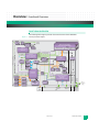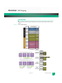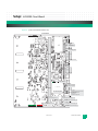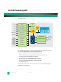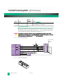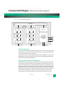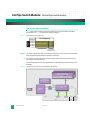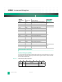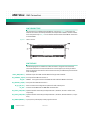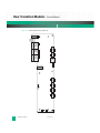
1
User’s Manual from Emerson Network Power ™ Embedded Computing KAT4000: AMC Carrier for ATCA® April 2007 The information in this manual has been checked and is believed to be accurate and reliable. HOWEVER, NO RESPONSIBILITY IS ASSUMED BY ARTESYN COMMUNICATION PRODUCTS FOR ITS USE OR FOR ANY INACCURACIES. Specifications are subject to change without notice. ARTESYN COMMUNICATION PRODUCTS DOES NOT ASSUME ANY LIABILITY ARISING OUT OF USE OR OTHER APPLICATION OF ANY PRODUCT, CIRCUIT, OR PROGRAM DESCRIBED HEREIN. This document does not convey any license under Artesyn Communication Products patents or the rights of others. Artesyn and the Artesyn logo are registered trademarks of Artesyn Technologies and are used by Artesyn Communication Products under license from Artesyn Technologies. All other trademarks are property of their respective owners. Revision Level: Principal Changes: Date: 10007175-00 Original release January 2007 10007175-01 Added “Appendix A” February 2007 10007175-02 Added PCIe functionality; Released 10 GbE-1 GbE fat pipe switch April 2007 Copyright © 2007 Artesyn Communication Products. All rights reserved. Emerson. Consider It Solved is a trademark, and Business-Critical Continuity, Emerson Network Power, and the Emerson Network Power logo are trademarks and service marks of Emerson Electric Co. © 2007 Emerson Electric Co. Regulatory Agency Warnings & Notices The Emerson KAT4000 meets the requirements set forth by the Federal Communications Commission (FCC) in Title 47 of the Code of Federal Regulations. The following information is provided as required by this agency. This device complies with part 15 of the FCC Rules. Operation is subject to the following two conditions: (1) This device may not cause harmful interference, and (2) this device must accept any interference received, including interference that may cause undesired operation. FCC RULES AND REGULATIONS — PART 15 This equipment has been tested and found to comply with the limits for a Class B digital device, pursuant to part 15 of the FCC Rules. These limits are designed to provide reasonable protection against harmful interference in a residential installation. This equipment generates, uses and can radiate radio frequency energy and, if not installed and used in accordance with the instructions, may cause harmful interference to radio communications. However, there is no guarantee that interference will not occur in a particular installation. If this equipment does cause harmful interference to radio or television reception, which can be determined by turning the equipment off and on, the user is encouraged to try to correct the interference by one or more of the following measures: • Reorient or relocate the receiving antenna • Increase the separation between the equipment and receiver • Connect the equipment into an outlet on a circuit different from that to which the receiver is connected • Consult the dealer or an experienced radio/TV technician for help Caution: Making changes or modifications to the KAT4000 hardware without the explicit consent of Emerson Network Power could invalidate the user’s authority to operate this equipment. ! EMC COMPLIANCE The electromagnetic compatibility (EMC) tests used a KAT4000 model that includes a front panel assembly from Emerson Network Power. Caution: For applications where the KAT4000 is provided without a front panel, or where the front panel has been removed, your system chassis/enclosure must provide the required ! electromagnetic interference (EMI) shielding to maintain CE compliance. 10007175-02 KAT4000 User’s Manual i Regulatory Agency Warnings & Notices (continued) EC Declaration of Conformity According to EN 45014:1998 Manufacturer’s Name: Emerson Network Power Embedded Computing Manufacturer’s Address: 8310 Excelsior Drive Madison, Wisconsin 53717 Declares that the following product, in accordance with the requirements of 89/336/EEC, EMC Directive and 99/5/EC, RTTE Directive and their amending directives, Product: ATCA Carrier Model Name/Number: KAT4000/10007505-xx has been designed and manufactured to the following specifications: EN55022:1998 Information Technology Equipment, Radio disturbance characteristics, Limits and methods of measurement EN55024:1998 Information Technology Equipment, Immunity characteristics, Limits and methods of measurement EN300386 V.1.3.1 Electromagnetic compatibility and radio spectrum matters (ERM); Telecommunication network equipment; EMC requirements As manufacturer we hereby declare that the product named above has been designed to comply with the relevant sections of the above referenced specifications. This product complies with the essential health and safety requirements of the EMC Directive and RTTE Directive. We have an internal production control system that ensures compliance between the manufactured products and the technical documentation. Bill Fleury Compliance Engineer Issue date: April 3, 2007 ii KAT4000 User’s Manual 10007175-02 Contents 1 Overview Components and Features . . . . . . . . . . . 1-1 KAT4000 Options. . . . . . . . . . . . . . . . 1-3 Functional Overview . . . . . . . . . . . . . . . . 1-5 Physical Memory Map . . . . . . . . . . . . . . . 1-6 AMC Mapping . . . . . . . . . . . . . . . . . . . . . . 1-9 Additional Information . . . . . . . . . . . . . 1-10 Product Certification . . . . . . . . . . . .1-10 UL Certification . . . . . . . . . . . . . . . . .1-11 RoHS Compliance. . . . . . . . . . . . . . .1-11 Terminology and Notation . . . . . . .1-12 Technical References. . . . . . . . . . . .1-12 Machine State Register. . . . . . . . . . . 3-9 Peripheral Interface . . . . . . . . . . . . . . . . 3-10 MPC8548 Peripheral Modules . . . . . . . 3-11 Three-Speed Ethernet Controllers (TSEC) . . . . . . . . . . . . . . . . . . . . . . . . 3-11 Local Bus Controller (LBC) . . . . . . . 3-12 Chip Select Generation. . . . . . . . . . 3-12 Processor Reset and Clocking Signals. 3-12 MPC8548 Exception Handling . . . . . . . 3-13 JTAG/COP Interface . . . . . . . . . . . . . . . . 3-14 No Processor Configuration . . . . . . . . . 3-15 4 Common Switch Region 2 Setup Electrostatic Discharge . . . . . . . . . . . . . . 2-1 KAT4000 Circuit Board . . . . . . . . . . . . . . 2-1 Front Panel . . . . . . . . . . . . . . . . . . . . . 2-4 Connectors . . . . . . . . . . . . . . . . . . . . . 2-4 Header JP4 . . . . . . . . . . . . . . . . . . . . . . 2-5 Jumpers . . . . . . . . . . . . . . . . . . . . . . . . 2-5 JTAG Interfaces . . . . . . . . . . . . . . . . . . 2-9 LEDs . . . . . . . . . . . . . . . . . . . . . . . . . .2-10 Reset. . . . . . . . . . . . . . . . . . . . . . . . . .2-13 KAT4000 Setup . . . . . . . . . . . . . . . . . . . . 2-15 Identification Numbers . . . . . . . . . .2-15 Power Requirements . . . . . . . . . . . .2-16 Environmental Considerations . . .2-16 Troubleshooting . . . . . . . . . . . . . . . . . . . 2-17 Technical Support . . . . . . . . . . . . . .2-17 Product Repair . . . . . . . . . . . . . . . . .2-18 3 Central Processing Unit MPC8548 Functions . . . . . . . . . . . . . . . . . 3-3 Microprocessor Core (e500). . . . . . . . . . 3-3 L1 Cache. . . . . . . . . . . . . . . . . . . . . . . . 3-3 L2 Cache. . . . . . . . . . . . . . . . . . . . . . . . 3-3 Timer/Counter . . . . . . . . . . . . . . . . . . 3-4 PCI Device and Vendor ID Assignment. 3-4 L2 Control Register (L2CR) . . . . . . . . 3-4 Hardware Implementation Dependent 0 Register. . . . . . . . . . . . . . . . . . . . . . . 3-6 Hardware Implementation Dependent 1 Register. . . . . . . . . . . . . . . . . . . . . . . 3-7 Interrupts and Exception Processing. . . 3-8 10007175-02 Ethernet Core Switch (optional) . . . . . . .4-2 Switch Configuration . . . . . . . . . . . . 4-3 High-Speed Serial Data Path Configuration . . . . . . . . . . . . . . . . . . . 4-3 On-Board Path Device Settings 4-4 Off-Board Path Device Settings 4-4 Ethernet Transceivers . . . . . . . . . . . . 4-5 Ethernet Address for the KAT4000 . . . . .4-5 Ethernet Address for the GbE Fat Pipe Switch Module . . . . . . . . . . . . . . . . . . . . . . . . . . . . .4-6 PCI Express Switch (optional) . . . . . . . . . .4-7 PCI Express Interface . . . . . . . . . . . . . 4-8 EEPROM Interface . . . . . . . . . . . . . . . 4-9 JTAG Controller Interface . . . . . . . . . 4-9 5 Fat Pipe Switch Module GbE Fat Pipe Switch Module . . . . . . . . . . .5-2 GbE Fat Pipe Switch Module Circuit Board . . . . . . . . . . . . . . . . . . . . . . . . . . 5-4 Components and Features. . . . . . . . 5-5 GbE Fat Pipe Switch Module PLD . . 5-6 Product ID/Version Register . . 5-6 Scratch Register . . . . . . . . . . . . . 5-7 I2C Register. . . . . . . . . . . . . . . . . 5-7 Signal Detect Register . . . . . . . 5-8 Switch Reset Register . . . . . . . . 5-8 Module Status Register . . . . . . 5-8 Switch GPIO Register . . . . . . . . 5-9 GPIN/LED Register . . . . . . . . . . . 5-9 10 GbE-1 GbE Fat Pipe Switch Module 5-11 10 GbE-1 GbE Fat Pipe Switch Module Circuit Board. . . . . . . . . . . . . . . . . . . 5-13 Components and Features. . . . . . . 5-14 KAT4000 User’s Manual iii Contents (continued) 10 GbE-1 GbE Fat Pipe Switch Module PLD . . . . . . . . . . . . . . . . . . . . . . . . . . . 5-16 Product ID/Version Register. . 5-16 Scratch Register . . . . . . . . . . . .5-17 I2C Register . . . . . . . . . . . . . . . .5-17 Reserved Register 1 . . . . . . . . .5-18 Switch Reset Register . . . . . . . 5-18 Module Status Register . . . . . . 5-19 Switch GPIO Register. . . . . . . . 5-19 GPIN/LED Register . . . . . . . . . . 5-20 10 GbE-10 GbE Fat Pipe Switch Module5-21 sRIO Fat Pipe Switch Module . . . . . . . . 5-22 6 Memory Configuration Boot Memory Configuration . . . . . . . . . .6-1 User Flash. . . . . . . . . . . . . . . . . . . . . . . . . . .6-1 On-Card SDRAM . . . . . . . . . . . . . . . . . . . . .6-2 NAND Flash . . . . . . . . . . . . . . . . . . . . . . . . .6-2 NVRAM Allocation . . . . . . . . . . . . . . . . . . .6-3 7 CPLD PLD Register Summary . . . . . . . . . . . . . . .7-1 Version and ID Registers . . . . . . . . . . . . . .7-2 Product ID Register (PIDR) . . . . . . . . 7-2 Hardware Version Register (HVR) . . 7-3 PLD Version Register (PVR) . . . . . . . 7-3 Configuration Registers . . . . . . . . . . . . . .7-4 Hardware Configuration Register 0 (HCR0) . . . . . . . . . . . . . . . . . . . . . . . . . 7-4 PLL Configuration Register (PLLC). . 7-4 Miscellaneous Registers . . . . . . . . . . . . . .7-5 LED Control Register (LEDR). . . . . . . 7-5 Jumper Settings Register (JSR). . . . . 7-6 RTM GPIO State Register (RGSR). . . 7-6 RTM GPIO Control Register (RGCR) 7-7 MISC Control Register (MISC) . . . . . 7-7 Scratch Register 1 (SCR1) . . . . . . . . . 7-8 Boot and Reset Registers . . . . . . . . . . . . .7-8 Reset Event Register (RER) . . . . . . . . 7-8 Reset Command Register 1 (RCR1) 7-9 Reset Command Register 2 (RCR2)7-10 Boot Device Redirection Register (BDRR) . . . . . . . . . . . . . . . . . . . . . . . .7-11 Clock Synchronizer Registers . . . . . . . . 7-13 Clock Synchronizer Control Registers 13 (CSC1—CSC3) . . . . . . . . . . . . . . . . . 7-13 iv KAT4000 User’s Manual 10007175-02 Clock Synchronizer Primary Source Registers 1-3 (CPS1—CPS3) . . . . . . 7-14 Clock Synchronizer Secondary Source Registers 1-3 (CSS1—CSS3) . . . . . . 7-15 Clock Control Registers (CCR1—CCR14) 7-17 Clock Synchronizer Interrupt Registers (CSI1-CSI3) . . . . . . . . . . . . . . . . . . . . 7-18 JTAG Interface . . . . . . . . . . . . . . . . . . . . . 7-19 8 AMC Sites AMC Connectors . . . . . . . . . . . . . . . . . . . .8-2 AMC Signals. . . . . . . . . . . . . . . . . . . . . . . . .8-2 Pin Assignments . . . . . . . . . . . . . . . . . . . . .8-4 SATA Lines . . . . . . . . . . . . . . . . . . . . . . . . . .8-6 9 System Management IPMC Overview . . . . . . . . . . . . . . . . . . . . . .9-1 IPMI Messaging. . . . . . . . . . . . . . . . . . . . . .9-3 IPMI Completion Codes . . . . . . . . . . 9-4 IPMB Protocol . . . . . . . . . . . . . . . . . . . . . . .9-5 SIPL Protocol . . . . . . . . . . . . . . . . . . . . . . . .9-6 Message Bridging . . . . . . . . . . . . . . . . . . . .9-7 Standard Commands. . . . . . . . . . . . . . . . .9-9 Vendor Commands . . . . . . . . . . . . . . . . 9-12 Get Status Command . . . . . . . . . . . 9-12 Get Serial Interface Properties Command . . . . . . . . . . . . . . . . . . . . . 9-14 Set Serial Interface Properties Command . . . . . . . . . . . . . . . . . . . . . 9-15 Get Debug Level Command . . . . . 9-16 Set Debug Level Command . . . . . . 9-17 Get Hardware Address Command 9-17 Set Hardware Address Command 9-18 Get Handle Switch Command. . . . 9-18 Set Handle Switch Command . . . . 9-19 Get Payload Communication Time-Out Command . . . . . . . . . . . . . . . . . . . . . 9-19 Set Payload Communication Time-Out Command . . . . . . . . . . . . . . . . . . . . . 9-20 Enable Payload Control Command9-20 Disable Payload Control Command . . . 9-20 Reset IPMC Command . . . . . . . . . . 9-21 Hang IPMC Command . . . . . . . . . . 9-21 Bused Resource Control Command . . . 9-22 Contents (continued) Bused Resource Status Command 9-22 Graceful Reset Command. . . . . . . . 9-23 Diagnostic Interrupt Results . . . . .9-24 Get Payload Shutdown Time-Out Command . . . . . . . . . . . . . . . . . . . . . 9-24 Set Payload Shutdown Time-Out Command . . . . . . . . . . . . . . . . . . . . . 9-25 Get Module State Command . . . . . 9-25 Enable AMC Site Command . . . . . . 9-26 Disable AMC Site Command . . . . .9-26 IPMC Watchdog Timer Commands. . . 9-27 Watchdog Timer Actions . . . . . . . . 9-27 Watchdog Timer Use Field and Expiration Flags . . . . . . . . . . . . . . . . 9-27 Using the Timer Use Field and Expiration Flags. . . . . . . . . . . . . 9-28 Watchdog Timer Event Logging . . 9-28 Monitor Support for Watchdog Timer . . . . . . . . . . . . . . . . . . . . . 9-29 Reset Watchdog Timer Command9-29 Set Watchdog Timer Command . . 9-29 Get Watchdog Timer Command. . 9-31 FRU LEDs . . . . . . . . . . . . . . . . . . . . . . . . . 9-33 Get FRU LED Properties Command9-34 Get LED Color Capabilities Command . 9-34 Set FRU LED State Command. . . . . 9-36 Get FRU LED State Command . . . . 9-38 Entities and Entity Associations . . . . . . 9-39 Sensors and Sensor Data Records . . . . 9-40 FRU Inventory . . . . . . . . . . . . . . . . . . . . . 9-44 E-Keying . . . . . . . . . . . . . . . . . . . . . . . . . . 9-45 Base Point-to-Point Connectivity . 9-45 Carrier Point-to-Point Connectivity9-46 Firmware Upgrade . . . . . . . . . . . . . . . . . 9-47 Firmware Upgrade Status Command . . 9-47 Firmware Upgrade Start Command . . . 9-48 Firmware Upgrade Prepare Command 9-49 Firmware Upgrade Write Command . . 9-49 Firmware Upgrade Complete Command . . . . . . . . . . . . . . . . . . . . . 9-50 Firmware Upgrade Restore Backup Command . . . . . . . . . . . . . . . . . . . . . 9-50 Firmware Upgrade Backup Revision Command . . . . . . . . . . . . . . . . . . . . . 9-51 10007175-02 Firmware Upgrade Termination . . 9-51 Firmware Upgrade Sequence . . . . 9-51 10 Synchronization Clocks MT9045 and MT9046 Clock Synchronizers . 10-2 11 Real-Time Clock Block Diagram. . . . . . . . . . . . . . . . . . . . . 11-1 Operation . . . . . . . . . . . . . . . . . . . . . . . . 11-1 Clock Operation . . . . . . . . . . . . . . . . . . . 11-2 12 Connectors Zone 1 . . . . . . . . . . . . . . . . . . . . . . . . . . . 12-1 Zone 2 . . . . . . . . . . . . . . . . . . . . . . . . . . . 12-2 Zone 3 . . . . . . . . . . . . . . . . . . . . . . . . . . . 12-4 13 Rear Transition Module Components and Features . . . . . . . . . . 13-1 Functional Overview . . . . . . . . . . . . . . . 13-2 Circuit Board . . . . . . . . . . . . . . . . . . . . . . 13-3 Face Plate. . . . . . . . . . . . . . . . . . . . . . . . . 13-5 Connectors . . . . . . . . . . . . . . . . . . . . . . . 13-5 Console Serial Ports. . . . . . . . . . . . . 13-5 Ethernet Port . . . . . . . . . . . . . . . . . . 13-6 Zone 3 . . . . . . . . . . . . . . . . . . . . . . . . 13-6 Setup . . . . . . . . . . . . . . . . . . . . . . . . . . . . 13-6 Identification Numbers . . . . . . . . . 13-7 Installation. . . . . . . . . . . . . . . . . . . . . . . . 13-7 14 Monitor Command-Line Features. . . . . . . . . . . . 14-1 Basic Operation . . . . . . . . . . . . . . . . . . . 14-4 Power-up/Reset Sequence . . . . . . 14-4 POST Diagnostic Results . . . . . . . . 14-6 Monitor SDRAM Usage . . . . . . . . . . 14-6 Monitor Recovery and Updates . . . . . . 14-6 Recovering the Monitor . . . . . . . . . 14-7 Resetting Environment Variables . 14-7 Updating the Monitor via TFTP . . . 14-7 Monitor Command Reference . . . . . . . 14-8 Command Syntax . . . . . . . . . . . . . . 14-8 Command Help . . . . . . . . . . . . . . . . 14-9 KAT4000 User’s Manual v Contents (continued) Typographic Conventions . . . . . . . 14-9 Boot Commands. . . . . . . . . . . . . . . . . . . 14-9 bootd . . . . . . . . . . . . . . . . . . . . . . . . . 14-9 bootelf . . . . . . . . . . . . . . . . . . . . . . . .14-9 bootm . . . . . . . . . . . . . . . . . . . . . . . .14-9 bootp . . . . . . . . . . . . . . . . . . . . . . . . . 14-9 bootv . . . . . . . . . . . . . . . . . . . . . . . .14-10 bootvx . . . . . . . . . . . . . . . . . . . . . . .14-10 dhcp . . . . . . . . . . . . . . . . . . . . . . . . .14-10 rarpboot. . . . . . . . . . . . . . . . . . . . . .14-11 tftpboot . . . . . . . . . . . . . . . . . . . . . .14-11 File Load Commands . . . . . . . . . . . . . . 14-12 loadb . . . . . . . . . . . . . . . . . . . . . . . .14-12 loads . . . . . . . . . . . . . . . . . . . . . . . . .14-12 Memory Commands . . . . . . . . . . . . . . 14-12 cmp. . . . . . . . . . . . . . . . . . . . . . . . . .14-13 cp . . . . . . . . . . . . . . . . . . . . . . . . . . .14-13 find . . . . . . . . . . . . . . . . . . . . . . . . . .14-13 md. . . . . . . . . . . . . . . . . . . . . . . . . . .14-13 mm . . . . . . . . . . . . . . . . . . . . . . . . . .14-14 nm. . . . . . . . . . . . . . . . . . . . . . . . . . .14-14 mw . . . . . . . . . . . . . . . . . . . . . . . . . .14-14 Flash Commands . . . . . . . . . . . . . . . . . 14-15 cp . . . . . . . . . . . . . . . . . . . . . . . . . . .14-15 erase . . . . . . . . . . . . . . . . . . . . . . . . .14-15 flinfo . . . . . . . . . . . . . . . . . . . . . . . . .14-15 protect . . . . . . . . . . . . . . . . . . . . . . .14-16 EEPROM/I2C Commands . . . . . . . . . . 14-16 eeprom . . . . . . . . . . . . . . . . . . . . . .14-16 icrc32 . . . . . . . . . . . . . . . . . . . . . . . .14-17 iloop . . . . . . . . . . . . . . . . . . . . . . . . .14-17 imd . . . . . . . . . . . . . . . . . . . . . . . . . .14-17 imd2 . . . . . . . . . . . . . . . . . . . . . . . . .14-17 imm . . . . . . . . . . . . . . . . . . . . . . . . .14-17 imm2 . . . . . . . . . . . . . . . . . . . . . . . .14-17 imw. . . . . . . . . . . . . . . . . . . . . . . . . .14-18 inm . . . . . . . . . . . . . . . . . . . . . . . . . .14-18 iprobe . . . . . . . . . . . . . . . . . . . . . . . .14-18 iprobe2. . . . . . . . . . . . . . . . . . . . . . .14-18 switchsrom . . . . . . . . . . . . . . . . . . .14-18 IPMC Commands . . . . . . . . . . . . . . . . . 14-18 fru . . . . . . . . . . . . . . . . . . . . . . . . . . .14-18 fruinit . . . . . . . . . . . . . . . . . . . . . . . .14-19 fruled . . . . . . . . . . . . . . . . . . . . . . . .14-19 ipmcfw . . . . . . . . . . . . . . . . . . . . . . .14-19 sensor. . . . . . . . . . . . . . . . . . . . . . . .14-19 Environment Parameter Commands 14-20 vi KAT4000 User’s Manual 10007175-02 printenv. . . . . . . . . . . . . . . . . . . . . . 14-21 saveenv . . . . . . . . . . . . . . . . . . . . . . 14-21 setenv . . . . . . . . . . . . . . . . . . . . . . . 14-21 Test Commands . . . . . . . . . . . . . . . . . . 14-21 diags. . . . . . . . . . . . . . . . . . . . . . . . . 14-21 mtest . . . . . . . . . . . . . . . . . . . . . . . . 14-21 um . . . . . . . . . . . . . . . . . . . . . . . . . . 14-22 Other Commands. . . . . . . . . . . . . . . . . 14-22 autoscr. . . . . . . . . . . . . . . . . . . . . . . 14-22 base . . . . . . . . . . . . . . . . . . . . . . . . . 14-22 bdinfo . . . . . . . . . . . . . . . . . . . . . . . 14-22 coninfo . . . . . . . . . . . . . . . . . . . . . . 14-22 crc32 . . . . . . . . . . . . . . . . . . . . . . . . 14-22 date . . . . . . . . . . . . . . . . . . . . . . . . . 14-22 echo . . . . . . . . . . . . . . . . . . . . . . . . . 14-23 enumpci . . . . . . . . . . . . . . . . . . . . . 14-23 go . . . . . . . . . . . . . . . . . . . . . . . . . . . 14-23 help . . . . . . . . . . . . . . . . . . . . . . . . . 14-23 iminfo . . . . . . . . . . . . . . . . . . . . . . . 14-23 isdram . . . . . . . . . . . . . . . . . . . . . . . 14-23 loop . . . . . . . . . . . . . . . . . . . . . . . . . 14-24 memmap . . . . . . . . . . . . . . . . . . . . 14-24 moninit . . . . . . . . . . . . . . . . . . . . . . 14-24 pci. . . . . . . . . . . . . . . . . . . . . . . . . . . 14-24 phy . . . . . . . . . . . . . . . . . . . . . . . . . . 14-25 ping . . . . . . . . . . . . . . . . . . . . . . . . . 14-25 reset . . . . . . . . . . . . . . . . . . . . . . . . . 14-25 run . . . . . . . . . . . . . . . . . . . . . . . . . . 14-26 script . . . . . . . . . . . . . . . . . . . . . . . . 14-26 showmac. . . . . . . . . . . . . . . . . . . . . 14-26 showpci . . . . . . . . . . . . . . . . . . . . . . 14-26 sleep. . . . . . . . . . . . . . . . . . . . . . . . . 14-26 switch_reg . . . . . . . . . . . . . . . . . . . 14-27 version . . . . . . . . . . . . . . . . . . . . . . . 14-27 vlan. . . . . . . . . . . . . . . . . . . . . . . . . . 14-27 Environment Variables . . . . . . . . . . . . 14-28 Troubleshooting. . . . . . . . . . . . . . . . . . 14-31 Download Formats. . . . . . . . . . . . . . . . 14-32 Binary. . . . . . . . . . . . . . . . . . . . . . . . 14-32 Motorola S-Record . . . . . . . . . . . . 14-32 15 Acronym List 16 Appendix A No-CPU KAT4000 . . . . . . . . . . . . . . . . . . . .A-1 Contents (continued) Ethernet Switch Configuration . . . . . . . A-2 Default Switch Configuration . . . . . A-2 Serial Command Line Interface (CLI). . . A-3 Log In/Log Out Procedures. . . . . . . . A-3 Help Utility. . . . . . . . . . . . . . . . . . . . . . A-3 Command Hierarchy . . . . . . . . . . . . . A-4 Command Usage Instructions . . . . . A-5 Commands . . . . . . . . . . . . . . . . . . . . . A-5 Command Overview . . . . . . . . . A-6 System Commands . . . . . . . . . . A-8 Console Commands . . . . . . . . . A-8 Port Commands . . . . . . . . . . . . . A-9 MAC Commands . . . . . . . . . . .A-10 10007175-02 VLAN Commands . . . . . . . . . . A-12 Aggregation/Trunking Commands A-13 User Group Commands . . . . . A-14 QoS Commands. . . . . . . . . . . . A-14 Mirror Commands . . . . . . . . . . A-16 IP Commands . . . . . . . . . . . . . . A-16 Debug Commands . . . . . . . . . A-17 Web Interface . . . . . . . . . . . . . . . . . . . . . A-18 17 Appendix B Sensor Data Records . . . . . . . . . . . . . . . . .B-1 KAT4000 User’s Manual vii (blank page) viii KAT4000 User’s Manual 10007175-02 Figures Figure 1-1: General System Block Diagram. . . . . . . . . . . . . . . . . . . . . . . . . . . . . . . . . . . . . . . . . . . . . . 1-5 Figure 1-2: KAT4000 Memory Map. . . . . . . . . . . . . . . . . . . . . . . . . . . . . . . . . . . . . . . . . . . . . . . . . . . . . 1-6 Figure 1-3: AMC Port Mapping Regions. . . . . . . . . . . . . . . . . . . . . . . . . . . . . . . . . . . . . . . . . . . . . . . . . 1-9 Figure 2-1: Component Map, Top (Rev. 02) . . . . . . . . . . . . . . . . . . . . . . . . . . . . . . . . . . . . . . . . . . . . . 2-2 Figure 2-2: Component Map, Bottom (Rev. 02). . . . . . . . . . . . . . . . . . . . . . . . . . . . . . . . . . . . . . . . . . 2-3 Figure 2-3: KAT4000 Front Panel . . . . . . . . . . . . . . . . . . . . . . . . . . . . . . . . . . . . . . . . . . . . . . . . . . . . . . 2-4 Figure 2-4: Jumper, Fuse and Switch Locations, Top . . . . . . . . . . . . . . . . . . . . . . . . . . . . . . . . . . . . . . 2-7 Figure 2-5: Jumper, Fuse and Switch Locations, Bottom . . . . . . . . . . . . . . . . . . . . . . . . . . . . . . . . . . 2-8 Figure 2-6: JTAG Hubs . . . . . . . . . . . . . . . . . . . . . . . . . . . . . . . . . . . . . . . . . . . . . . . . . . . . . . . . . . . . . . . . 2-9 Figure 2-7: LEDs, Top. . . . . . . . . . . . . . . . . . . . . . . . . . . . . . . . . . . . . . . . . . . . . . . . . . . . . . . . . . . . . . . . 2-11 Figure 2-8: LEDs, Bottom . . . . . . . . . . . . . . . . . . . . . . . . . . . . . . . . . . . . . . . . . . . . . . . . . . . . . . . . . . . . 2-12 Figure 2-9: KAT4000 Reset Diagram . . . . . . . . . . . . . . . . . . . . . . . . . . . . . . . . . . . . . . . . . . . . . . . . . . 2-14 Figure 3-1: MPC8548 Block Diagram . . . . . . . . . . . . . . . . . . . . . . . . . . . . . . . . . . . . . . . . . . . . . . . . . . . 3-2 Figure 3-2: Processor JTAG/COP Diagram . . . . . . . . . . . . . . . . . . . . . . . . . . . . . . . . . . . . . . . . . . . . . . 3-14 Figure 3-3: Processor JTAG/COP Header . . . . . . . . . . . . . . . . . . . . . . . . . . . . . . . . . . . . . . . . . . . . . . . 3-14 Figure 4-1: Board Area Network . . . . . . . . . . . . . . . . . . . . . . . . . . . . . . . . . . . . . . . . . . . . . . . . . . . . . . . 4-1 Figure 4-2: VSC7376 GbE Switch Block Diagram . . . . . . . . . . . . . . . . . . . . . . . . . . . . . . . . . . . . . . . . . 4-3 Figure 4-3: PEX 8524 Block Diagram . . . . . . . . . . . . . . . . . . . . . . . . . . . . . . . . . . . . . . . . . . . . . . . . . . . 4-8 Figure 4-4: PEX 8524 SPI EEPROM Interface . . . . . . . . . . . . . . . . . . . . . . . . . . . . . . . . . . . . . . . . . . . . . 4-9 Figure 5-1: AMC Port Map Fat Pipes Region–GbE . . . . . . . . . . . . . . . . . . . . . . . . . . . . . . . . . . . . . . . . 5-2 Figure 5-2: Signal Routing of the GbE Fat Pipe Switch Module on the KAT4000 . . . . . . . . . . . . . . 5-2 Figure 5-3: GbE Fat Pipe Switch Module Block Diagram . . . . . . . . . . . . . . . . . . . . . . . . . . . . . . . . . . . 5-3 Figure 5-4: GbE Fat Pipe Switch Module Component Map, Top (Rev. 00). . . . . . . . . . . . . . . . . . . . 5-4 Figure 5-5: GbE Fat Pipe Switch Module Component Map, Bottom (Rev. 00) . . . . . . . . . . . . . . . . 5-4 Figure 5-6: GbE Fat Pipe Switch JTAG . . . . . . . . . . . . . . . . . . . . . . . . . . . . . . . . . . . . . . . . . . . . . . . . . . . 5-5 Figure 5-7: GbE Fat Pipe Switch Reset . . . . . . . . . . . . . . . . . . . . . . . . . . . . . . . . . . . . . . . . . . . . . . . . . . 5-6 Figure 5-8: AMC Port Map Fat Pipes Region–10 GbE-1 GbE . . . . . . . . . . . . . . . . . . . . . . . . . . . . . . 5-11 Figure 5-9: Signal Routing of the 10 GbE-1 GbE Fat Pipe Switch Module on the KAT4000 . . . . 5-11 Figure 5-10: 10 GbE-1 GbE Fat Pipe Switch Module Block Diagram . . . . . . . . . . . . . . . . . . . . . . . . . 5-12 Figure 5-11: 10 GbE-1 GbE Fat Pipe Switch Module Component Map, Top (Rev. 01) . . . . . . . . . . 5-13 Figure 5-12: 10 GbE-1 GbE Fat Pipe Switch Module Component Map, Bottom (Rev. 01) . . . . . . 5-13 Figure 5-13: 10 GbE-1 GbE Fat Pipe Switch JTAG . . . . . . . . . . . . . . . . . . . . . . . . . . . . . . . . . . . . . . . . . 5-15 Figure 5-14: 10 GbE-1 GbE Fat Pipe Switch Reset . . . . . . . . . . . . . . . . . . . . . . . . . . . . . . . . . . . . . . . . 5-16 Figure 5-15: AMC Port Map Fat Pipes Region–10 GbE-10 GbE . . . . . . . . . . . . . . . . . . . . . . . . . . . . . 5-21 Figure 5-16: Signal Routing of the 10 GbE-10 GbE Fat Pipe Switch Module on the KAT4000 . . . 5-21 Figure 5-17: AMC Port Map Fat Pipes Region–sRIO . . . . . . . . . . . . . . . . . . . . . . . . . . . . . . . . . . . . . . 5-22 Figure 5-18: Signal Routing of the sRIO Fat Pipe Switch Module on the KAT4000. . . . . . . . . . . . . 5-22 Figure 7-1: Boot Device Redirection. . . . . . . . . . . . . . . . . . . . . . . . . . . . . . . . . . . . . . . . . . . . . . . . . . . 7-12 Figure 7-2: PLD JTAG Diagram . . . . . . . . . . . . . . . . . . . . . . . . . . . . . . . . . . . . . . . . . . . . . . . . . . . . . . . . 7-20 Figure 8-1: AMC B+ Connector . . . . . . . . . . . . . . . . . . . . . . . . . . . . . . . . . . . . . . . . . . . . . . . . . . . . . . . . 8-2 10007175-02 KAT4000 User’s Manual ix Figures x (continued) KAT4000 User’s Manual Figure 8-2: Diagram of SATA line connections . . . . . . . . . . . . . . . . . . . . . . . . . . . . . . . . . . . . . . . . . . . 8-6 Figure 9-1: IPMC Connections Block Diagram . . . . . . . . . . . . . . . . . . . . . . . . . . . . . . . . . . . . . . . . . . . 9-2 Figure 9-2: Extension Command Request Example. . . . . . . . . . . . . . . . . . . . . . . . . . . . . . . . . . . . . . . 9-7 Figure 9-3: Extension Command Response Example . . . . . . . . . . . . . . . . . . . . . . . . . . . . . . . . . . . . . 9-7 Figure 9-4: IPMB Entity Structure . . . . . . . . . . . . . . . . . . . . . . . . . . . . . . . . . . . . . . . . . . . . . . . . . . . . . 9-40 Figure 10-1: Synchronization Clock Circuit Diagram. . . . . . . . . . . . . . . . . . . . . . . . . . . . . . . . . . . . . . 10-1 Figure 11-1: M41T00 Real-Time Clock Block Diagram . . . . . . . . . . . . . . . . . . . . . . . . . . . . . . . . . . . . 11-1 Figure 12-1: Zone 1 Connector, P10. . . . . . . . . . . . . . . . . . . . . . . . . . . . . . . . . . . . . . . . . . . . . . . . . . . . 12-1 Figure 12-2: Zone 2 Connectors, J20 and J23, and Zone 3 Connectors, J30-J32. . . . . . . . . . . . . . . 12-3 Figure 12-3: Zone 3 Connector, J33 . . . . . . . . . . . . . . . . . . . . . . . . . . . . . . . . . . . . . . . . . . . . . . . . . . . . 12-7 Figure 13-1: RTM General System Block Diagram with Face Plate . . . . . . . . . . . . . . . . . . . . . . . . . . 13-2 Figure 13-2: RTM Component Map, Top (Rev. 00) . . . . . . . . . . . . . . . . . . . . . . . . . . . . . . . . . . . . . . . 13-4 Figure 13-3: Micro-D Console Cable . . . . . . . . . . . . . . . . . . . . . . . . . . . . . . . . . . . . . . . . . . . . . . . . . . . . 13-5 Figure 13-4: Standard Console Cable Wiring, #10007665-xx . . . . . . . . . . . . . . . . . . . . . . . . . . . . . . 13-6 Figure 13-5: Installing a KAT-Z3DB RTM on the KAT4000 . . . . . . . . . . . . . . . . . . . . . . . . . . . . . . . . . 13-8 Figure 14-1: Example Monitor Start-up Display for KAT4000 with GbE Fat Pipe Switch Module 14-2 Figure 14-2: ule Example Monitor Start-up Display for KAT4000 with 10 GbE-1 GbE Fat Pipe Switch Mod. . . . . . . . . . . . . . . . . . . . . . . . . . . . . . . . . . . . . . . . . . . . . . . . . . . . . . . . . . . . . . . . . . . . . . . . 14-3 Figure 14-3: Power-up/Reset Sequence Flowchart . . . . . . . . . . . . . . . . . . . . . . . . . . . . . . . . . . . . . . . 14-5 Figure A-1: No-CPU KAT4000 System Block Diagram . . . . . . . . . . . . . . . . . . . . . . . . . . . . . . . . . . . . . A-1 Figure A-2: Web Interface for the Ethernet Core Switch. . . . . . . . . . . . . . . . . . . . . . . . . . . . . . . . . . A-20 10007175-02 Tables Table 1-1: KAT4000 Address Summary . . . . . . . . . . . . . . . . . . . . . . . . . . . . . . . . . . . . . . . . . . . . . . . . 1-7 Table 1-2: Regulatory Agency Compliance . . . . . . . . . . . . . . . . . . . . . . . . . . . . . . . . . . . . . . . . . . . . 1-10 Table 1-3: Technical References . . . . . . . . . . . . . . . . . . . . . . . . . . . . . . . . . . . . . . . . . . . . . . . . . . . . . 1-12 Table 2-1: Circuit Board Dimensions . . . . . . . . . . . . . . . . . . . . . . . . . . . . . . . . . . . . . . . . . . . . . . . . . . 2-1 Table 2-2: JP4 Signal Descriptions . . . . . . . . . . . . . . . . . . . . . . . . . . . . . . . . . . . . . . . . . . . . . . . . . . . . . 2-5 Table 2-3: Jumpers–JP2 and JP7 . . . . . . . . . . . . . . . . . . . . . . . . . . . . . . . . . . . . . . . . . . . . . . . . . . . . . . 2-6 Table 2-4: J35 Signal Descriptions . . . . . . . . . . . . . . . . . . . . . . . . . . . . . . . . . . . . . . . . . . . . . . . . . . . . 2-10 Table 2-5: Typical Power Requirement. . . . . . . . . . . . . . . . . . . . . . . . . . . . . . . . . . . . . . . . . . . . . . . . 2-16 Table 2-6: Environmental Requirements . . . . . . . . . . . . . . . . . . . . . . . . . . . . . . . . . . . . . . . . . . . . . . 2-16 Table 2-7: Air Flow Requirements . . . . . . . . . . . . . . . . . . . . . . . . . . . . . . . . . . . . . . . . . . . . . . . . . . . . 2-16 Table 3-1: MPC8548 Features . . . . . . . . . . . . . . . . . . . . . . . . . . . . . . . . . . . . . . . . . . . . . . . . . . . . . . . . 3-1 Table 3-2: PCI Device and Vendor ID. . . . . . . . . . . . . . . . . . . . . . . . . . . . . . . . . . . . . . . . . . . . . . . . . . . 3-4 Table 3-3: MPC8548 Peripheral Request Priority . . . . . . . . . . . . . . . . . . . . . . . . . . . . . . . . . . . . . . . 3-10 Table 3-4: MPC8548 Chip Select . . . . . . . . . . . . . . . . . . . . . . . . . . . . . . . . . . . . . . . . . . . . . . . . . . . . . 3-12 Table 3-5: MPC8548 Exceptions . . . . . . . . . . . . . . . . . . . . . . . . . . . . . . . . . . . . . . . . . . . . . . . . . . . . . 3-13 Table 3-6: Processor JTAG/COP Pin Assignments (P1). . . . . . . . . . . . . . . . . . . . . . . . . . . . . . . . . . . 3-15 Table 4-1: KAT4000 PHYs and Address Values . . . . . . . . . . . . . . . . . . . . . . . . . . . . . . . . . . . . . . . . . . 4-4 Table 4-2: Ethernet Core Switch Off-Board Ports . . . . . . . . . . . . . . . . . . . . . . . . . . . . . . . . . . . . . . . . 4-4 Table 4-3: GbE Fat Pipe Module Ethernet Switch Off-Board Ports. . . . . . . . . . . . . . . . . . . . . . . . . . 4-5 Table 4-4: Ethernet Port Address Numbering . . . . . . . . . . . . . . . . . . . . . . . . . . . . . . . . . . . . . . . . . . . 4-6 Table 4-5: PEX 8524 JTAG Signals . . . . . . . . . . . . . . . . . . . . . . . . . . . . . . . . . . . . . . . . . . . . . . . . . . . . . 4-9 Table 5-1: GbE Fat Pipe PLD Registers . . . . . . . . . . . . . . . . . . . . . . . . . . . . . . . . . . . . . . . . . . . . . . . . . 5-6 Table 5-2: BCM56580 Switch Ports. . . . . . . . . . . . . . . . . . . . . . . . . . . . . . . . . . . . . . . . . . . . . . . . . . . 5-14 Table 5-3: 10 GbE-1 GbE Fat Pipe PLD Registers . . . . . . . . . . . . . . . . . . . . . . . . . . . . . . . . . . . . . . . . 5-16 Table 6-1: Memory Configuration Jumper . . . . . . . . . . . . . . . . . . . . . . . . . . . . . . . . . . . . . . . . . . . . . . 6-1 NVRAM Memory Map, User EEPROM 1 (write protected)1 . . . . . . . . . . . . . . . . . . . . . . 6-3 Table 6-2: Table 6-3: NVRAM Memory Map, User EEPROM 2 . . . . . . . . . . . . . . . . . . . . . . . . . . . . . . . . . . . . . . . 6-3 Table 7-1: PLD Registers . . . . . . . . . . . . . . . . . . . . . . . . . . . . . . . . . . . . . . . . . . . . . . . . . . . . . . . . . . . . . 7-1 Table 7-2: JP3 PLD JTAG Pin Assignments . . . . . . . . . . . . . . . . . . . . . . . . . . . . . . . . . . . . . . . . . . . . . 7-19 Table 7-3: JP1 Pin Assignments . . . . . . . . . . . . . . . . . . . . . . . . . . . . . . . . . . . . . . . . . . . . . . . . . . . . . . 7-20 Table 8-1: B1-B4 AMC Pin Assignments . . . . . . . . . . . . . . . . . . . . . . . . . . . . . . . . . . . . . . . . . . . . . . . . 8-4 Table 9-1: Network Function Codes . . . . . . . . . . . . . . . . . . . . . . . . . . . . . . . . . . . . . . . . . . . . . . . . . . . 9-3 Table 9-2: Completion Codes. . . . . . . . . . . . . . . . . . . . . . . . . . . . . . . . . . . . . . . . . . . . . . . . . . . . . . . . . 9-4 Table 9-3: Format for IPMI Request Message . . . . . . . . . . . . . . . . . . . . . . . . . . . . . . . . . . . . . . . . . . . 9-5 Table 9-4: Format for IPMI Response Message . . . . . . . . . . . . . . . . . . . . . . . . . . . . . . . . . . . . . . . . . . 9-6 Table 9-5: IPMC IPMI Commands . . . . . . . . . . . . . . . . . . . . . . . . . . . . . . . . . . . . . . . . . . . . . . . . . . . . . 9-9 Table 9-6: Vendor Command Summary . . . . . . . . . . . . . . . . . . . . . . . . . . . . . . . . . . . . . . . . . . . . . . 9-12 Table 9-7: Get Status Command . . . . . . . . . . . . . . . . . . . . . . . . . . . . . . . . . . . . . . . . . . . . . . . . . . . . . 9-13 Table 9-8: Get Serial Interface Properties Command . . . . . . . . . . . . . . . . . . . . . . . . . . . . . . . . . . . 9-14 Table 9-9: Set Serial Interface Properties Command . . . . . . . . . . . . . . . . . . . . . . . . . . . . . . . . . . . . 9-15 10007175-02 KAT4000 User’s Manual xi Tables xii (continued) KAT4000 User’s Manual Table 9-10: Get Debug Level Command . . . . . . . . . . . . . . . . . . . . . . . . . . . . . . . . . . . . . . . . . . . . . . . 9-16 Table 9-11: Set Debug Level Command . . . . . . . . . . . . . . . . . . . . . . . . . . . . . . . . . . . . . . . . . . . . . . . . 9-17 Table 9-12: Get Hardware Address Command . . . . . . . . . . . . . . . . . . . . . . . . . . . . . . . . . . . . . . . . . . 9-17 Table 9-13: Set Hardware Address Command . . . . . . . . . . . . . . . . . . . . . . . . . . . . . . . . . . . . . . . . . . 9-18 Table 9-14: Get Handle Switch Command. . . . . . . . . . . . . . . . . . . . . . . . . . . . . . . . . . . . . . . . . . . . . . 9-18 Table 9-15: Set Handle Switch Command . . . . . . . . . . . . . . . . . . . . . . . . . . . . . . . . . . . . . . . . . . . . . . 9-19 Table 9-16: Get Payload Communication Time-Out Command . . . . . . . . . . . . . . . . . . . . . . . . . . . 9-19 Table 9-17: Set Payload Communication Time-Out Command. . . . . . . . . . . . . . . . . . . . . . . . . . . . 9-20 Table 9-18: Disable Payload Control Command . . . . . . . . . . . . . . . . . . . . . . . . . . . . . . . . . . . . . . . . . 9-20 Table 9-19: Reset IPMC Command . . . . . . . . . . . . . . . . . . . . . . . . . . . . . . . . . . . . . . . . . . . . . . . . . . . . 9-21 Table 9-20: Hang IPMC Command . . . . . . . . . . . . . . . . . . . . . . . . . . . . . . . . . . . . . . . . . . . . . . . . . . . . 9-21 Table 9-21: Bused Resource Control Command . . . . . . . . . . . . . . . . . . . . . . . . . . . . . . . . . . . . . . . . . 9-22 Table 9-22: Bused Resource Status Command . . . . . . . . . . . . . . . . . . . . . . . . . . . . . . . . . . . . . . . . . . 9-23 Table 9-23: Graceful Reset Command . . . . . . . . . . . . . . . . . . . . . . . . . . . . . . . . . . . . . . . . . . . . . . . . . 9-24 Table 9-24: Diagnostic Interrupt Results Command . . . . . . . . . . . . . . . . . . . . . . . . . . . . . . . . . . . . . 9-24 Table 9-25: Get Payload Shutdown Time-Out Command. . . . . . . . . . . . . . . . . . . . . . . . . . . . . . . . . 9-25 Table 9-26: Set Payload Shutdown Time-Out Command . . . . . . . . . . . . . . . . . . . . . . . . . . . . . . . . . 9-25 Table 9-27: Get Module State Command . . . . . . . . . . . . . . . . . . . . . . . . . . . . . . . . . . . . . . . . . . . . . . 9-25 Table 9-28: Enable AMC Site Command. . . . . . . . . . . . . . . . . . . . . . . . . . . . . . . . . . . . . . . . . . . . . . . . 9-26 Table 9-29: Disable AMC Site Command . . . . . . . . . . . . . . . . . . . . . . . . . . . . . . . . . . . . . . . . . . . . . . . 9-26 Table 9-30: IPMC Watchdog Timer Commands . . . . . . . . . . . . . . . . . . . . . . . . . . . . . . . . . . . . . . . . . 9-27 Table 9-31: Reset Watchdog Timer Command. . . . . . . . . . . . . . . . . . . . . . . . . . . . . . . . . . . . . . . . . . 9-29 Table 9-32: Set Watchdog Timer Command. . . . . . . . . . . . . . . . . . . . . . . . . . . . . . . . . . . . . . . . . . . . 9-30 Table 9-33: Get Watchdog Timer Command . . . . . . . . . . . . . . . . . . . . . . . . . . . . . . . . . . . . . . . . . . . 9-31 Table 9-34: FRU LEDs . . . . . . . . . . . . . . . . . . . . . . . . . . . . . . . . . . . . . . . . . . . . . . . . . . . . . . . . . . . . . . . . 9-33 Table 9-35: Get FRU LED Properties Command . . . . . . . . . . . . . . . . . . . . . . . . . . . . . . . . . . . . . . . . . 9-34 Table 9-36: Get LED Color Capabilities Command . . . . . . . . . . . . . . . . . . . . . . . . . . . . . . . . . . . . . . . 9-34 Table 9-37: Set FRU LED State Command . . . . . . . . . . . . . . . . . . . . . . . . . . . . . . . . . . . . . . . . . . . . . . 9-36 Table 9-38: Get FRU LED State Command . . . . . . . . . . . . . . . . . . . . . . . . . . . . . . . . . . . . . . . . . . . . . . 9-38 Table 9-39: IPMI Sensors . . . . . . . . . . . . . . . . . . . . . . . . . . . . . . . . . . . . . . . . . . . . . . . . . . . . . . . . . . . . . 9-40 Table 9-40: Event Message Format . . . . . . . . . . . . . . . . . . . . . . . . . . . . . . . . . . . . . . . . . . . . . . . . . . . . 9-43 Table 9-41: FRU Definitions . . . . . . . . . . . . . . . . . . . . . . . . . . . . . . . . . . . . . . . . . . . . . . . . . . . . . . . . . . 9-44 Table 9-42: Link Descriptors . . . . . . . . . . . . . . . . . . . . . . . . . . . . . . . . . . . . . . . . . . . . . . . . . . . . . . . . . . 9-45 Table 9-43: Firmware Upgrade Command Summary . . . . . . . . . . . . . . . . . . . . . . . . . . . . . . . . . . . . 9-47 Table 9-44: Firmware Upgrade Status Command . . . . . . . . . . . . . . . . . . . . . . . . . . . . . . . . . . . . . . . 9-47 Table 9-45: Firmware Upgrade Start Command. . . . . . . . . . . . . . . . . . . . . . . . . . . . . . . . . . . . . . . . . 9-48 Table 9-46: Firmware Upgrade Prepare Command . . . . . . . . . . . . . . . . . . . . . . . . . . . . . . . . . . . . . . 9-49 Table 9-47: Firmware Upgrade Write Command . . . . . . . . . . . . . . . . . . . . . . . . . . . . . . . . . . . . . . . . 9-50 Table 9-48: Firmware Upgrade Complete Command . . . . . . . . . . . . . . . . . . . . . . . . . . . . . . . . . . . . 9-50 Table 9-49: Firmware Upgrade Restore Backup Command . . . . . . . . . . . . . . . . . . . . . . . . . . . . . . . 9-51 Table 9-50: Firmware Upgrade Backup Revision Command . . . . . . . . . . . . . . . . . . . . . . . . . . . . . . 9-51 10007175-02 Tables (continued) Table 11-1: RTC Register Map . . . . . . . . . . . . . . . . . . . . . . . . . . . . . . . . . . . . . . . . . . . . . . . . . . . . . . . . 11-2 Table 12-1: Zone 1 Connector, P10 Pin Assignments . . . . . . . . . . . . . . . . . . . . . . . . . . . . . . . . . . . . 12-1 Table 12-2: Zone 2 Connector, J20 Pin Assignments . . . . . . . . . . . . . . . . . . . . . . . . . . . . . . . . . . . . . 12-3 Table 12-3: Zone 2 Connector, J23 Pin Assignments . . . . . . . . . . . . . . . . . . . . . . . . . . . . . . . . . . . . . 12-4 Table 12-4: Zone 3 Connector, J30 Pin Assignments . . . . . . . . . . . . . . . . . . . . . . . . . . . . . . . . . . . . . 12-5 Table 12-5: Zone 3 Connector, J31 Pin Assignments . . . . . . . . . . . . . . . . . . . . . . . . . . . . . . . . . . . . . 12-5 Table 12-6: Zone 3 Connector, J32 Pin Assignments . . . . . . . . . . . . . . . . . . . . . . . . . . . . . . . . . . . . . 12-6 Table 12-7: Zone 3 Connector, J33 Pin Assignments . . . . . . . . . . . . . . . . . . . . . . . . . . . . . . . . . . . . . 12-7 Table 13-1: RTM Circuit Board Dimensions . . . . . . . . . . . . . . . . . . . . . . . . . . . . . . . . . . . . . . . . . . . . . 13-3 Table 13-2: Console Serial Port Pin Assignments, P1, P2 and P4-P7 . . . . . . . . . . . . . . . . . . . . . . . . 13-5 Table 13-3: Ethernet Port Pin Assignments, P3. . . . . . . . . . . . . . . . . . . . . . . . . . . . . . . . . . . . . . . . . . 13-6 Table 14-1: Debug LED Codes . . . . . . . . . . . . . . . . . . . . . . . . . . . . . . . . . . . . . . . . . . . . . . . . . . . . . . . . 14-4 Table 14-2: POST Diagnostic Results–Bit Assignments . . . . . . . . . . . . . . . . . . . . . . . . . . . . . . . . . . 14-6 Table 14-3: Monitor Address per Flash Device . . . . . . . . . . . . . . . . . . . . . . . . . . . . . . . . . . . . . . . . . . 14-7 Table 14-4: Static IP Ethernet Configuration . . . . . . . . . . . . . . . . . . . . . . . . . . . . . . . . . . . . . . . . . . . 14-10 Table 14-5: DHCP Ethernet Configuration. . . . . . . . . . . . . . . . . . . . . . . . . . . . . . . . . . . . . . . . . . . . . 14-11 Table 14-6: Standard Environment Variables . . . . . . . . . . . . . . . . . . . . . . . . . . . . . . . . . . . . . . . . . . 14-28 Table 14-7: Optional Environment Variables. . . . . . . . . . . . . . . . . . . . . . . . . . . . . . . . . . . . . . . . . . . 14-30 Table A-1: General Command Types . . . . . . . . . . . . . . . . . . . . . . . . . . . . . . . . . . . . . . . . . . . . . . . . . . A-5 Table B-1: IPMI Sensor Data Record . . . . . . . . . . . . . . . . . . . . . . . . . . . . . . . . . . . . . . . . . . . . . . . . . . . B-1 Table B-2: KAT4000 IPMC SDR Description . . . . . . . . . . . . . . . . . . . . . . . . . . . . . . . . . . . . . . . . . . . . . B-2 Table B-3: Hot Swap SDR Description. . . . . . . . . . . . . . . . . . . . . . . . . . . . . . . . . . . . . . . . . . . . . . . . . . B-2 Table B-4: IPMB Physical SDR Description . . . . . . . . . . . . . . . . . . . . . . . . . . . . . . . . . . . . . . . . . . . . . . B-4 Table B-5: BMC Watchdog SDR Description . . . . . . . . . . . . . . . . . . . . . . . . . . . . . . . . . . . . . . . . . . . . B-5 Table B-6: +3.3 Volt SDR Description . . . . . . . . . . . . . . . . . . . . . . . . . . . . . . . . . . . . . . . . . . . . . . . . . . B-7 Table B-7: +2.5 Volt SDR Description . . . . . . . . . . . . . . . . . . . . . . . . . . . . . . . . . . . . . . . . . . . . . . . . . . B-9 Table B-8: +1.8 Volt SDR Description . . . . . . . . . . . . . . . . . . . . . . . . . . . . . . . . . . . . . . . . . . . . . . . . . B-11 Table B-9: +1.2 Volt SDR Description . . . . . . . . . . . . . . . . . . . . . . . . . . . . . . . . . . . . . . . . . . . . . . . . . B-13 Table B-10: +1.0 Volt SDR Description . . . . . . . . . . . . . . . . . . . . . . . . . . . . . . . . . . . . . . . . . . . . . . . . . B-15 Table B-11: CPU Volt SDR Description . . . . . . . . . . . . . . . . . . . . . . . . . . . . . . . . . . . . . . . . . . . . . . . . . B-17 Table B-12: Inflow Temp SDR Description . . . . . . . . . . . . . . . . . . . . . . . . . . . . . . . . . . . . . . . . . . . . . . B-19 Table B-13: Outflow Temp SDR Description . . . . . . . . . . . . . . . . . . . . . . . . . . . . . . . . . . . . . . . . . . . . B-21 Table B-14: Version Change SDR Description . . . . . . . . . . . . . . . . . . . . . . . . . . . . . . . . . . . . . . . . . . . B-24 Table B-15: B1 Hot Swap SDR Description . . . . . . . . . . . . . . . . . . . . . . . . . . . . . . . . . . . . . . . . . . . . . . B-25 Table B-16: B2 Hot Swap SDR Description . . . . . . . . . . . . . . . . . . . . . . . . . . . . . . . . . . . . . . . . . . . . . . B-27 Table B-17: B3 Hot Swap SDR Description . . . . . . . . . . . . . . . . . . . . . . . . . . . . . . . . . . . . . . . . . . . . . . B-28 Table B-18: B4 Hot Swap SDR Description . . . . . . . . . . . . . . . . . . . . . . . . . . . . . . . . . . . . . . . . . . . . . . B-30 Table B-19: B1 +12V Current SDR Description . . . . . . . . . . . . . . . . . . . . . . . . . . . . . . . . . . . . . . . . . . B-31 Table B-20: B1 +12V Volt SDR Description . . . . . . . . . . . . . . . . . . . . . . . . . . . . . . . . . . . . . . . . . . . . . B-33 Table B-21: B2 +12V Current SDR Description . . . . . . . . . . . . . . . . . . . . . . . . . . . . . . . . . . . . . . . . . . B-35 Table B-22: B2 +12V Volt SDR Description . . . . . . . . . . . . . . . . . . . . . . . . . . . . . . . . . . . . . . . . . . . . . B-36 10007175-02 KAT4000 User’s Manual xiii Tables xiv (continued) KAT4000 User’s Manual Table B-23: B3 +12V Current SDR Description . . . . . . . . . . . . . . . . . . . . . . . . . . . . . . . . . . . . . . . . . . B-38 Table B-24: B3 +12V Volt SDR Description . . . . . . . . . . . . . . . . . . . . . . . . . . . . . . . . . . . . . . . . . . . . . B-40 Table B-25: B4 +12V Current SDR Description . . . . . . . . . . . . . . . . . . . . . . . . . . . . . . . . . . . . . . . . . . B-41 Table B-26: B4 +12V Volt SDR Description . . . . . . . . . . . . . . . . . . . . . . . . . . . . . . . . . . . . . . . . . . . . . B-43 Table B-27: -48V Volt SDR Description . . . . . . . . . . . . . . . . . . . . . . . . . . . . . . . . . . . . . . . . . . . . . . . . . B-45 Table B-28: -48V Current SDR Description. . . . . . . . . . . . . . . . . . . . . . . . . . . . . . . . . . . . . . . . . . . . . . B-47 Table B-29: -48V Source A Volt SDR Description . . . . . . . . . . . . . . . . . . . . . . . . . . . . . . . . . . . . . . . . B-48 Table B-30: -48V Source B Volt SDR Description . . . . . . . . . . . . . . . . . . . . . . . . . . . . . . . . . . . . . . . . B-50 Table B-31: +3.3V Management SDR Description . . . . . . . . . . . . . . . . . . . . . . . . . . . . . . . . . . . . . . . B-52 Table B-32: +12V Volt SDR Description . . . . . . . . . . . . . . . . . . . . . . . . . . . . . . . . . . . . . . . . . . . . . . . . B-54 Table B-33: -12V Current SDR Description. . . . . . . . . . . . . . . . . . . . . . . . . . . . . . . . . . . . . . . . . . . . . . B-56 Table B-34: F/W (Firmware) Progress SDR Description . . . . . . . . . . . . . . . . . . . . . . . . . . . . . . . . . . . B-58 10007175-02 Registers Register 3-1: L2 Control Register (L2CR). . . . . . . . . . . . . . . . . . . . . . . . . . . . . . . . . . . . . . . . . . . . . . . . . . 3-4 Register 3-2: MPC8548 Hardware Implementation Dependent Register 0 (HID0) . . . . . . . . . . . . . 3-6 Register 3-3: MPC8548 Hardware Implementation Dependent Register 1 (HID1) . . . . . . . . . . . . . 3-8 Register 3-4: CPU Machine State Register (MSR) . . . . . . . . . . . . . . . . . . . . . . . . . . . . . . . . . . . . . . . . . . 3-9 Register 5-1: Product ID/Version Register (PIDV) at 0x00 . . . . . . . . . . . . . . . . . . . . . . . . . . . . . . . . . . . 5-7 Register 5-2: Scratch Register (SCR) at 0x01 . . . . . . . . . . . . . . . . . . . . . . . . . . . . . . . . . . . . . . . . . . . . . . 5-7 Register 5-3: I2C Register (I2C) at 0x02 . . . . . . . . . . . . . . . . . . . . . . . . . . . . . . . . . . . . . . . . . . . . . . . . . . 5-7 Register 5-4: Signal Detect Register (SDET) at 0x03. . . . . . . . . . . . . . . . . . . . . . . . . . . . . . . . . . . . . . . . 5-8 Register 5-5: Switch Reset Register (SRST) at 0x04 . . . . . . . . . . . . . . . . . . . . . . . . . . . . . . . . . . . . . . . . 5-8 Register 5-6: Module Status Register (STAT) at 0x05 . . . . . . . . . . . . . . . . . . . . . . . . . . . . . . . . . . . . . . . 5-9 Register 5-7: Switch GPIO Register (GPIO) at 0x06 . . . . . . . . . . . . . . . . . . . . . . . . . . . . . . . . . . . . . . . . . 5-9 Register 5-8: GPIN/LED Register (GPLED) at 0x07 . . . . . . . . . . . . . . . . . . . . . . . . . . . . . . . . . . . . . . . . . 5-10 Register 5-9: Product ID/Version Register (PIDV) at 0x00 . . . . . . . . . . . . . . . . . . . . . . . . . . . . . . . . . . 5-16 Register 5-10: Scratch Register (SCR) at 0x01 . . . . . . . . . . . . . . . . . . . . . . . . . . . . . . . . . . . . . . . . . . . . . 5-17 Register 5-11: I2C Register (I2C) at 0x02 . . . . . . . . . . . . . . . . . . . . . . . . . . . . . . . . . . . . . . . . . . . . . . . . . 5-17 Register 5-12: Reserved Register 1 at 0x03 . . . . . . . . . . . . . . . . . . . . . . . . . . . . . . . . . . . . . . . . . . . . . . . 5-18 Register 5-13: Switch Reset Register (SRST) at 0x04 . . . . . . . . . . . . . . . . . . . . . . . . . . . . . . . . . . . . . . . 5-18 Register 5-14: Module Status Register (STAT) at 0x05 . . . . . . . . . . . . . . . . . . . . . . . . . . . . . . . . . . . . . . 5-19 Register 5-15: Switch GPIO Register (GPIO) at 0x06 . . . . . . . . . . . . . . . . . . . . . . . . . . . . . . . . . . . . . . . . 5-19 Register 5-16: GPIN/LED Register (GPLED) at 0x07 . . . . . . . . . . . . . . . . . . . . . . . . . . . . . . . . . . . . . . . . . 5-20 Register 7-1: Product ID Register (PIDR) at 0xfc40,0000. . . . . . . . . . . . . . . . . . . . . . . . . . . . . . . . . . . . 7-2 Register 7-2: Hardware Version Register (HVR) at 0xfc40,0004 . . . . . . . . . . . . . . . . . . . . . . . . . . . . . 7-3 Register 7-3: PLD Version Register (PVR) at 0xfc40,0008 . . . . . . . . . . . . . . . . . . . . . . . . . . . . . . . . . . . 7-3 Register 7-4: Hardware Configuration Register 0 (HCR0) at 0xfc40,0010 . . . . . . . . . . . . . . . . . . . . . 7-4 Register 7-5: PLL Configuration Register (PLLC) at 0xfc40,000c . . . . . . . . . . . . . . . . . . . . . . . . . . . . . 7-4 Register 7-6: LED Control Register (LEDR) at 0xfc40,001c . . . . . . . . . . . . . . . . . . . . . . . . . . . . . . . . . . 7-5 Register 7-7: Jumper Settings Register (JSR) at 0xfc40,0018 . . . . . . . . . . . . . . . . . . . . . . . . . . . . . . . . 7-6 Register 7-8: RTM GPIO State Register (RGSR) at 0xfc40,0038 . . . . . . . . . . . . . . . . . . . . . . . . . . . . . . 7-6 Register 7-9: RTM GPIO Control Register (RGCR) at 0xfc40,003c . . . . . . . . . . . . . . . . . . . . . . . . . . . . 7-7 Register 7-10: MISC Control Register (MISC) at 0xfc40,0034 . . . . . . . . . . . . . . . . . . . . . . . . . . . . . . . . . 7-7 Register 7-11: Scratch Register 1 (SCR1) at 0xfc40,002c. . . . . . . . . . . . . . . . . . . . . . . . . . . . . . . . . . . . . 7-8 Register 7-12: Reset Event Register (RER) at 0xfc40,0020. . . . . . . . . . . . . . . . . . . . . . . . . . . . . . . . . . . . 7-9 Register 7-13: Reset Command Register 1 (RCR1) at 0xfc40,0024 . . . . . . . . . . . . . . . . . . . . . . . . . . . . 7-9 Register 7-14: Reset Command Register 2 (RCR2) at 0xfc40,0028 . . . . . . . . . . . . . . . . . . . . . . . . . . . 7-10 Register 7-15: Boot Device Redirection Register (BDRR) at 0xfc40,0030 . . . . . . . . . . . . . . . . . . . . . . 7-12 Register 7-16: Clock Synchronizer Control Registers 1-3 (CSC1-CSC3) at 0xfc40,0040, 0xfc40,0044, 0xfc40,0048, respectively . . . . . . . . . . . . . . . . . . . . . . . . . . . . . . . . . . . . . . . . . . . . . . . . . . . . . . . . . . . . . . . 7-13 Register 7-17: Clock Synchronizer Primary Source Registers 1-3 (CPS1-CPS3) at 0xfc40,0050, 0xfc40,0054, 0xfc40,0058, respectively . . . . . . . . . . . . . . . . . . . . . . . . . . . . . . . . . . . . . . . . . . . . . . . . . . . 7-14 Register 7-18: Clock Synchronizer Secondary Source Registers 1-3 (CSS1-CSS3) at 0xfc40,0060, 0xfc40,0064, 0xfc40,0068, respectively . . . . . . . . . . . . . . . . . . . . . . . . . . . . . . . . . . . . . . . . . . . . . . . . . . . 7-15 10007175-02 KAT4000 User’s Manual i Registers (continued) Register 7-19: Clock Control Registers 1-14 (CCR1-CCR14) at 0xfc40,0070, 0xfc40,0074, 0xfc40,0078, 0xfc40,007c, 0xfc40,0080, 0xfc40,0084, 0xfc40,0088, 0xfc40,008c, 0xfc40,0090, 0xfc40,0094, 0xfc40,0098, 0xfc40,009c, 0xfc40,00a0, 0xfc40,00a4, respectively . . . . . . . . . . . . . . 7-17 Register 7-20: Clock Synchronizer Interrupt Registers 1-3 (CSI1-CSI3) at 0xfc40,00a8, 0xfc40,00ac, 0xfc40,00b0, respectively . . . . . . . . . . . . . . . . . . . . . . . . . . . . . . . . . . . . . . . . . . . . . . . . . . . . . . . . . . . . . . . 7-18 Register 9-1: ii KAT4000 User’s Manual Enable Payload Control Command . . . . . . . . . . . . . . . . . . . . . . . . . . . . . . . . . . . . . . . . . 9-20 10007175-02 Section 1 Overview The KAT4000 is a single-slot Advanced Telecom Computing Architecture (AdvancedTCA®, ATCA™) carrier with up to four Advanced Mezzanine Cards (AMC) expansion modules. This expansion capability enables a wide variety of control and packet processing applications such as WAN access, traffic processing, signaling gateways, media gateways, and many others. ATCA is an open architecture telecom platform as defined by the PICMG® 3.0 Revision 2.0 AdvancedTCA™ Base Specification. The KAT4000 features on-board Ethernet and PCI Express switches for the AdvancedMC Common Options Region, where the majority of control plane data flows, and a flexible modular Fat Pipe Switch (FPS) to address data plane traffic in the AdvancedMC Fat Pipes Region. The FPS is implemented using a plug-over module, enabling simple maintenance and a rapid upgrade path when a newer switch fabric is required. An optional on-board processor gives users additional processing power and can be used to off-load system management or OA&M functionality. The KAT4000 is an intelligent Field Replaceable Unit (FRU) and implements a redundant System Management Bus (SMB). It also fully supports the Intelligent Platform Management Interface (IPMI) with AdvancedTCA extensions to support standards-based shelf management, allowing it to be monitored by a local shelf management controller or by a remote OA&M system over Ethernet. COMPONENTS AND FEATURES The following is a brief summary of the KAT4000 hardware components and features: Processor: The Central Processing Unit (CPU) is a Freescale® Semiconductor MPC8548 PowerQUICC III™ processor, operating at a rate of up to 1.3 GHz with a 533 MHz DDR2 bus. The MPC8548 contains 32-kB separate level-one (L1) data and instruction caches, and 512-kB L2 cache. The processor has a local bus that connects to the socketed, NOR, and NAND flash; Ethernet core switch; fat pipe switch module; and PLD. The processor also has a COP/JTAG for debugging purposes. Chapter 3 provides more information. SDRAM: The KAT4000 includes a 64M x 72-bit Double Data Rate Two (DDR2) Synchronous Dynamic Random Access Memory (SDRAM) Small-Outline Dual In-line Memory Module (SO-DIMM). Options include 512 megabytes and 1 gigabyte. The interface implements eight additional bits to permit the use of Error-Correcting Code (ECC). SDRAM is only implemented on the processor KAT4000 board configuration. “On-Card SDRAM” on page 6-2 provides more information. Flash: The KAT4000 includes three independent Flash regions—socketed, NOR, and NAND. The blade is capable of booting from either an 8-bit, 32-pin PLCC ROM socket up to 512 kilobytes in size, or from a 16-bit NOR Flash region that consists of one or two Flash devices. 10007175-02 KAT4000 User’s Manual 1-1 Overview: Components and Features The NOR Flash consists of two 16 megabyte banks. The supported NAND flash is 512 megabytes or 1 gigabyte. Flash is only implemented on the processor KAT4000 board configuration. Chapter 6 provides more information. CPLD: The KAT4000 uses a Complex Programmable Logic Device (CPLD) to control board reset logic, the Board Configuration, Board Revision and User LED registers, and miscellaneous board logic. Register access to the PLD is only available on the processor KAT4000 board configuration. Chapter 7 provides more information. Ethernet: Depending on the configuration, the KAT4000 Ethernet interface consists of: Reduced Gigabit (RGMII)/Serial Gigabit (SGMII)/1000Base-BX Serializer-Deserializer (SerDes) Ethernet core or fat pipe switch module (Vitesse VSC7376), and 1000Base-BX (SerDes) devices to the AMC sites. One 10/100 eTSEC port from the MPC8548 is available through Zone 3 for Rear Transition Module (RTM) access. This port is for development purposes only. Serial I/O: An EIA-232 console serial port from the MPC8548 (serial 1) is available through an on-board header and is optionally routable to Zone 3 for Rear Transition Module (RTM) access. The default serial port settings are: 9,600 baud, 8 data, no parity, and 1 stop bit. This port is for development purposes only. A second serial port (serial 2) allows the MPC8548 to communicate with the Intelligent Platform Management Controller (IPMC). The default serial port settings are: 115,200 baud, 8 data, no parity, and 1 stop bit. I2C Bus: The private IPMC I2C bus consists of the following devices: temp sensors, the -48V converter, AMC A-to-D converters, and an optional connection to Zone 3 for Rear Transition Module (RTM) access. One processor I2C bus links to the following: two user SEEPROMs, the CPU init SEEPROM, the Real-Time Clock (RTC), the SO-DIMM, and the fat pipe switch module, if used. Another processor I2C bus provides an optional connection to Zone 3 for Rear Transition Module (RTM) access. JTAG Hubs: The IPMC controls the two Joint Test Action Group (JTAG) interfaces (hubs). One JTAG hub is connected to seven ports: the KSL PLD, the IPMC PLD, the fat pipe switch module, and the four AMC sites. The other hub is connected to five ports: the VSC7376 switch, the PEX8524 switch, the clock synchronizers, the IPMC GPIO, and GbE PHYs. See “JTAG Interfaces” on page 2-9 for more information. AMC Sites: The KAT4000 has four single-width, mid-size Advanced Mezzanine Card (AMC) sites which allow for use of up to four compatible AMC modules. Double-width and compact modules can also be accommodated. B+ style AMC connectors are used. The KAT4000 complies 1-2 KAT4000 User’s Manual 10007175-02 Overview: Components and Features with the PICMG® AMC.0 Revision 2.0 Advanced Mezzanine Card Base Specification with the exception of a couple non-conformances. See the KAT4000 Errata for details. Each AMC site is individually configurable. Chapter 8 provides more information. System Management: The KAT4000 supports an Intelligent Platform Management Interface (IPMI) based on a Renesas microcontroller with a UART interface for processor to IPMC communication (fixed rate at 115,200 baud) and dual redundant IPMB-A/B interfaces. The IPMC allows for features such as remote shutdown, remote reset, payload voltage monitoring, temperature monitoring, and access to Field Replaceable Unit (FRU) data. Chapter 9 provides more information. Synchronization Clock: The synchronization clock interface consists of MT9045 or MT9046 T1/E1 system synchronizers. Chapter 10 provides more information. RTC: The Real-Time Clock (RTC) is an ST®Microelectronics M41T00 Serial Access Timekeeper®. Chapter 11 provides more information. Caution: There are no serviceable parts in this product. Return all damaged boards to Emerson for repair (see page 2-18). ! KAT4000 Options No-CPU Configuration: A no-CPU KAT4000 board configuration is available. This configuration includes 256 Kb of SRAM memory used by the internal 8051 microcontroller on the VSC7376 Ethernet core switch for run time code storage. This configuration omits SDRAM and NOR and NAND flash. Appendix A provides more information. Ethernet Core Switch: The Ethernet core switch provides the interconnect between the fat pipe switch module, the Ethernet ports on the AMC sites, two channels on the ATCA backplane Base fabric, the processor, and the Update Channel (optional). A Vitesse VSC7376 GbE switch implements this function. “Ethernet Core Switch (optional)” on page 4-2 provides more information. PCI Express Switch: The PCIe switch provides the interconnect between the AMC sites, the processor, and the fat pipe switch module. A PLX Technology PEX 8524 PCIe switch implements this function. “PCI Express Switch (optional)” on page 4-7 provides more information. Note: Of the Ethernet core switch and the PCI Express switch, at least one of the two switches must be used on the board. The board can also use both switches. 10007175-02 KAT4000 User’s Manual 1-3 Overview: Components and Features Fat Pipe Switch Module: A high-speed fat pipe switch is provided as a plug-over module. It supports GbE, Serial Rapid IO (sRIO), PCI Express (PCIe) or 10 Gigabit Ethernet (10 GbE). This switch provides an interconnect between the AMC sites, the ATCA high-speed fabric ports, the processor, the PCIe switch and the Ethernet core switch. See “Fat Pipe Switch Module”, Chapter 5, for information on your module’s configuration. Rear Transition Module (RTM): The optional transition modules provide access to 16 or 32 ports when AMCs are installed on the KAT4000. AMC site ports 12-20 are routed to Zone 3 for Rear Transition Module (RTM) I/O. 64 AMC signals route to 264 pins in Zone 3 (see “Zone 3” on page 12-4). There are nine T1/E1 ports per AMC site routed as differential pairs (64 signals). There are separate I2C connections to the IPMC and the processor, and two ports each from the fat pipe switch module and the Ethernet Core switch. A serial port and GbE port are provided for development purposes only. 1-4 KAT4000 User’s Manual 10007175-02 Overview: Functional Overview FUNCTIONAL OVERVIEW The following block diagram provides a functional overview for the KAT4000: Figure 1-1: General System Block Diagram To Zone 3 (Optional) NAND Flash Main PLD RTC User 1 SEEPROM GbE PHY PCIe (x1 or x4) User 2 SEEPROM GbE To Zone 3 SERDES GbE sRIO (x4) SROM DDR2-667 2GB -48V Cnvrtr Private I2C AMC A-to-D I 2C Clock IPMC I 2C Fat Pipe 3 To Zone 3 RGMII Xfmr Xfmr (2) 2 IPMB Sensors Base 10007175-02 EIA-232 Xcvr Serial Header 4 SERDES (no conn. for GbE) Fat Pipe Switch Module Fabric Options: GbE, sRIO, 10-1 GbE or 10-10 GbE High Speed Fabric A J23 P10 To processor GMII/RGMII PCIe GbE PHYs (2) PLD Socketed Flash MPC8548 Processor CPU Init SEEPROM PCIe or GbE on port 1 Serial 2 NOR Flash To Update Channel on J20 (Optional) 4 SERDES Optional GbE PHYs (2) SO-DIMM 4 SERDES SERDES SERDES SERDES 2 SGMII Local bus Serial 1 10/100 Debug Eth (MII) VSC7376 Ethernet Core Switch Layer 2 (Optional) 2 SERDES IPMB-L I2C PEX8524 PCI Express Switch (Optional) To Zone 3 2 SERDES To local bus AMC (x4) Single-Width, Half-/Full-/Extended-Height Serial Header 4 SERDES EIA-232 Transceiver To local bus Xfmr 4 SERDES 10/100 PHY High Speed Fabric B To Eth Core Switch (Opt.) 2 4 Clock J20 To Eth Core Switch 9 2 Zone 3 Connections (Opt.) RTM I/O (Optional) Zone 3 KAT4000 User’s Manual 1-5 Overview: Physical Memory Map PHYSICAL MEMORY MAP Fig. 1-2 illustrates the KAT4000 memory map: Figure 1-2: KAT4000 Memory Map Hex Address FC40,00B0 FC40,00AC FC40,00A8 FC40,00A4 Hex Address FFFF,FFFF FFF0,0000 FF80,0000 FF70,0000 FC88,0000 FC80,0000 FC48,0000 FC40,0000 FC18,0000 FC14,0000 FC40,00A0 FC40,009C FC40,0098 FC40,0094 Boot Area (1 MB) Reserved CCSRBAR (MPC8548 Registers, 1 MB) Reserved Socketed Flash (if installed) (512 KB) Reserved CPLD Registers (512 KB) Reserved Fat Pipe Switch Registers (if installed) (256 KB) Reserved FC12,0000 Ethernet Core Switch Registers (128 KB) FC10,0000 Reserved FC00,8000 NAND Flash (32 KB) FC00,0000 Reserved E200,0000 NOR Flash (32 MB) E000,0000 PCIe Switch or sRIO Fat Pipe Module (if installed) (1 GB) A000,0000 8000,0000 PCI Express Switch (if installed) (512 MB) 3FFF,FFFF Reserved 0000,0000 SDRAM DDR2 (512 MB) FC40,007C FC40,0078 FC40,0074 FC40,0070 FC40,006C FC40,0068 FC40,0064 FC40,0060 FC40,005C FC40,0058 FC40,0054 FC40,0050 FC40,004C FC40,0048 FC40,0044 FC40,0040 FC40,003C FC40,0038 FC40,0034 FC40,0030 FC40,002C FC40,0028 FC40,0024 Reserved 1FFF,FFFF FC40,0090 FC40,008C FC40,0088 FC40,0084 FC40,0080 SDRAM DDR2 (1 GB) FC40,0020 FC40,001C FC40,0018 FC40,0014 FC40,0010 FC40,000C FC40,0008 FC40,0004 FC40,0000 1-6 KAT4000 User’s Manual 10007175-02 Clock Sync. Interrupt Register 3 Clock Sync. Interrupt Register 2 Clock Sync. Interrupt Register 1 Clock Control, aTCA CLK3 B Register Clock Control, aTCA CLK3 A Register Clock Control, AMC4 CLK3 Register Clock Control, AMC4 CLK2 Register Clock Control, AMC4 CLK1 Register Clock Control, AMC3 CLK3 Register Clock Control, AMC3 CLK2 Register Clock Control, AMC3 CLK1 Register Clock Control, AMC2 CLK3 Register Clock Control, AMC2 CLK2 Register Clock Control, AMC2 CLK1 Register Clock Control, AMC1 CLK3 Register Clock Control, AMC1 CLK2 Register Clock Control, AMC1 CLK1 Register Reserved Clock Sync. Secondary Source 3 Clock Sync. Secondary Source 2 Clock Sync. Secondary Source 1 Reserved Clock Sync. Primary Source 3 Clock Sync. Primary Source 2 Clock Sync. Primary Source 1 Reserved Clock Sync. Control Register 3 Clock Sync. Control Register 2 Clock Sync. Control Register 1 RTM GPIO Control Register RTM GPIO State Register MISC Control Register Boot Device Redirection Register Scratch Register 1 Reset Command Register 2 Reset Command Register 1 Reset Event Register LED Control Register Jumper Settings Register Reserved Hardware Config. Register 0 PLL Configuration Register PLD Version Register Hardware Version Register Product ID Register Overview: Physical Memory Map Table 1-1 summarizes the physical addresses for the KAT4000 and provides references to more detailed information: Table 1-1: KAT4000 Address Summary Physical Address (hex): Access Mode: Description: FFF0,0000 R/W Boot Area (1 MB) – FF80,0000 – Reserved – See Page: FF70,0000 W – CCSRBAR (MPC8548 Registers, 1 MB) 1 – FC88,0000 Reserved – FC80,0000 R/W Socketed Flash (if installed) (512 KB) 6-1 FC48,0000 – Reserved – FC40,00B0 R/W Clock Synchronizer Interrupt Register 3 (CSI3) 7-18 FC40,00AC R/W Clock Synchronizer Interrupt Register 2 (CSI2) 7-18 FC40,00A8 R/W Clock Synchronizer Interrupt Register 1 (CSI1) 7-18 FC40,00A4 R/W Clock Control, aTCA CLK3 B Register (CCR14) 7-17 FC40,00A0 R/W Clock Control, aTCA CLK3 A Register (CCR13) 7-17 FC40,009C R/W Clock Control, AMC4 CLK3 Register (CCR12) 7-17 FC40,0098 R/W Clock Control, AMC4 CLK2 Register (CCR11) 7-17 FC40,0094 R/W Clock Control, AMC4 CLK1 Register (CCR10) 7-17 FC40,0090 R/W Clock Control, AMC3 CLK3 Register (CCR9) 7-17 FC40,008C R/W Clock Control, AMC3 CLK2 Register (CCR8) 7-17 FC40,0088 R/W Clock Control, AMC3 CLK1 Register (CCR7) 7-17 FC40,0084 R/W Clock Control, AMC2 CLK3 Register (CCR6) 7-17 FC40,0080 R/W Clock Control, AMC2 CLK2 Register (CCR5) 7-17 FC40,007C R/W Clock Control, AMC2 CLK1 Register (CCR4) 7-17 FC40,0078 R/W Clock Control, AMC1 CLK3 Register (CCR3) 7-17 FC40,0074 R/W Clock Control, AMC1 CLK2 Register (CCR2) 7-17 FC40,0070 R/W Clock Control, AMC1 CLK1 Register (CCR1) 7-17 FC40,006C – Reserved – FC40,0068 R/W Clock Synchronizer Secondary Source Register 3 (CSS3) 7-15 FC40,0064 R/W Clock Synchronizer Secondary Source Register 2 (CSS2) 7-15 FC40,0060 R/W Clock Synchronizer Secondary Source Register 1 (CSS1) 7-15 FC40,005C – Reserved – FC40,0058 R/W Clock Synchronizer Primary Source Register 3 (CPS3) 7-14 FC40,0054 R/W Clock Synchronizer Primary Source Register 2 (CPS2) 7-14 FC40,0050 R/W Clock Synchronizer Primary Source Register 1 (CPS1) 7-14 FC40,004C – Reserved – FC40,0048 R/W Clock Synchronizer Control Register 3 (CSC3) 7-13 FC40,0044 R/W Clock Synchronizer Control Register 2 (CSC2) 7-13 FC40,0040 R/W Clock Synchronizer Control Register 1 (CSC1) 7-13 10007175-02 KAT4000 User’s Manual 1-7 Overview: 1-8 Physical Memory Map Physical Address (hex): Access Mode: Description: See Page: (continued) FC40,003C R/W RTM GPIO Control Register (RGCR) 7-7 FC40,0038 R RTM GPIO State Register (RGSR) 7-6 FC40,0034 R/W MISC Control (PCIe, SIO, I2C, Test Clock) Register (MISC) 7-7 FC40,0030 R Boot Device Redirection Register (BDRR) 7-12 FC40,002C R/W Scratch Register 1 (SCR1) 7-8 FC40,0028 W Reset Command Register 2 (RCR2) 7-10 FC40,0024 W Reset Command Register 1 (RCR1) 7-9 FC40,0020 R Reset Event Register (RER) 7-9 FC40,001C R/W LED Control Register (LEDR) 7-5 FC40,0018 R Jumper Settings Register (JSR) 7-6 FC00,0014 – Reserved – FC40,0010 R Hardware Configuration Register 0 (HCR0) 7-4 FC40,000C R/W PLL Configuration Register (PLLC) 7-4 7-3 FC40,0008 R PLD Version Register (PVR) FC40,0004 R Hardware Version Register (HVR) 7-3 FC40,0000 R Product ID Register (PIDR) 7-2 FC18,0000 – Reserved – FC14,0000 R/W Fat Pipe Ethernet Switch Registers (if installed) (256 KB) 5-2 FC12,0000 – Reserved – FC10,0000 R/W Ethernet Core Switch Registers (128 KB) 4-2 FC00,8000 – Reserved – FC00,0000 R/W 6-2 E200,0000 – NAND Flash (32 KB) 1 Reserved E000,0000 R/W NOR Flash (32 MB) 6-1 A000,0000 R/W 4-7 or 5-22 – 8000,0000 R/W PCI Express Switch or sRIO Fat Pipe Switch Module (if installed) (1 GB)2 PCI Express Switch (if installed) (512 MB)2 4000,0000 – Reserved1 – 0000,0000 R/W SDRAM DDR2 (512 MB/1 GB) 6-2 4-7 1. Depends on Flash/memory size. 2. Both the PCI Express Switch and sRIO Fat Pipe Switch Module are optional. If both devices are discovered onboard, then the PCIe switch will be allocated 512 MB and the sRIO fat pipe switch module will be allocated 1 GB of addressable space. If neither device is found onboard, the entire 1.5 GB area is reserved. KAT4000 User’s Manual 10007175-02 Overview: AMC Mapping AMC MAPPING The figure below shows how the KAT4000 maps to the ports defined by the AMC.0 specification: Figure 1-3: AMC Port Mapping Regions Port # Basic Connector Port Mapping ()* ()* "#$ &-()* % &' +, . / +, ( ,"4 1/ / /6' ( ,"4 1/ #1'6/ &' ( ,"4 1/ / /6' Extended Connector ! ! % &' 01 3 2 ." Port # +, (4#5 6" ." ." 1 / B4 B3 B2 B1 ." 1 / 8 ! B2 ! B1 B3 ! ! 7 +, (4#5 6" ." 7 +, (4#5 6" ." 10007175-02 +, +, +, +, Port # &.% (4#5 6" ." B4 &.% &.% Port # +, +, +, +, Port # +, KAT4000 User’s Manual 1-9 Overview: Additional Information Clocks: This region supports a subset of the clock architecture, as defined in the AMC.0 specification. Common Options: This region supports essential interfaces that are common across multiple Fat Pipe implementations. Fat Pipes: This region supports data path connections including GbE, sRIO, PCIe, and 10 GbE. It can carry large amounts of data without significantly degrading the speed of transmission. Extended Options: This region supports Rear Transition Modules. Also, it may be used to extend the Common Options and Fat Pipes Regions, when required. x1, x2, x4: This refers to the link width of the port (the number of lanes that can be used to interconnect between two link partners). ADDITIONAL INFORMATION This section lists the KAT4000 hardware regulatory certifications and briefly discusses the terminology and notation conventions used in this manual. It also lists general technical references. Mean time between failures (MTBF) has been calculated at greater than 315,816 hours for the KAT4000 and greater than 264,795 hours for the KAT4000 with a GbE fat pipe switch module. MTBFs were calculated using Method I Case 3, Telcordia Issue 1 model at 30° C. Product Certification The KAT4000 hardware has been tested to comply with various safety, immunity, and emissions requirements as specified by the Federal Communications Commission (FCC), Industry Canada (IC), Underwriters Laboratories Inc.® (UL), and the European Union Directives (CE mark). The following table summarizes this compliance: Table 1-2: Regulatory Agency Compliance Type: Safety Specification: IEC60950/EN60950 – Safety of Information Technology Equipment (Western Europe) UL60950, CSA C22.2 No. 60950, Third Edition – Safety of Information Technology Equipment, including Electrical Business Equipment (BINational) AS/NZS 60950:2000 – Safety Standard for Australia and New Zealand Global IEC – CB Scheme Report IEC 60950, all country deviations 1-10 KAT4000 User’s Manual 10007175-02 Overview: Additional Information Type: Specification: (continued) Environmental NEBS™: Telcordia™ GR-63 (applies to an entire system) – Section 4.3 Equipment Handling Criteria; Section 4.4.1 Earthquake Environment and Criteria (Zone 4); Section 4.4.3 Office Vibration Environment and Criteria; Section 4.4.4 Transportation Vibration Criteria EMC FCC Part 15, Class B – Title 47, Code of Federal Regulations, Radio Frequency Devices ICES 003, Class A – Industry Canada Interference-causing Equipment Standard for Digital Apparatus NEBS: Telcordia GR-1089 level 3 – Emissions and Immunity (circuit pack level testing only) EN300386 – Electromagnetic Compatibility and Radio Spectrum Matters (ERM), Telecommunication Network Equipment, Electromagnetic Compatibility (EMC) Requirements AS/NZS 3548 003 – Standard for radiated and conducted emissions for Australia and New Zealand, Class A Emerson maintains test reports that provide specific information regarding the methods and equipment used in compliance testing. Unshielded external I/O cables, loose screws, or a poorly grounded chassis may adversely affect the KAT4000’s ability to comply with any of the stated specifications. UL Certification The UL web site at ul.com has a list of Emerson’s UL certifications. 1 To find the list, go to the web site and search in the online certifications directory using Emerson’s UL file number, E190079. There is a list for products distributed in the United States, as well as a list for products shipped to Canada. 2 Products are listed by board type followed by the model name and/or number. The KAT4000 is an AdvancedTCA (ATCA) blade. The model number is KAT4000’s Printed Circuit Board (PCB) artwork number, which is 10007505-xx. RoHS Compliance The KAT4000, all fat pipe modules listed in Chapter 5, and the RTM described in Chapter 13 are compliant with the European Union’s RoHS (Restriction of Use of Hazardous Substances) directive created to limit harm to the environment and human health by restricting the use of harmful substances in electrical and electronic equipment. Effective July 1, 2006, RoHS restricts the use of six substances: cadmium (Cd), mercury (Hg), hexavalent chromium (Cr (VI)), polybrominated biphenyls (PBBs), polybrominated diphenyl ethers 10007175-02 KAT4000 User’s Manual 1-11 Overview: Additional Information (PBDEs) and lead (Pb). Configurations that are RoHS compliant are built with lead-free solder. Configurations that are 5-of-6 are built with tin-lead solder per the lead-in-solder RoHS exemption. To obtain a certificate of conformity (CoC) for the KAT4000 or other modules, send an email to [email protected] or call 1-800-356-9602. Have the part number(s) (e.g., C000####-##) for your configuration(s) available when contacting Emerson. Terminology and Notation Active low signals: An active low signal is indicated with an asterisk * after the signal name. Byte, word: Throughout this manual byte refers to 8 bits, word refers to 16 bits, and long word refers to 32 bits, double long word refers to 64 bits. PLD: This manual uses the acronym, PLD, as a generic term for programmable logic device (also known as FPGA, CPLD, EPLD, etc.). Radix 2 and 16: Hexadecimal numbers end with a subscript 16 or begin with 0x. Binary numbers are shown with a subscript 2. Technical References Further information on basic operation and programming of the KAT4000 components can be found in the following documents: Table 1-3: Technical References Device / Interface: AMC/ATCA Document: 3 Advanced Mezzanine Card Base Specification (PICMG® AMC.0 Rev. 2.0: November 15, 2006) PCI Express and Advanced Switching on AdvancedMC (PICMG® AMC.1 Rev. 1.0: January 20, 2005) AdvancedTCA® Base Specification (PICMG® 3.0 Rev. 2.0: March 18, 2005) Engineering Change Notice 3.0-2.0-001 (PICMG® 3.0 Rev. 2.0: ECN 3.0-2.0-001; June 15, 2005) AdvancedTCA® Ethernet/Fibre Channel for AdvancedTCA® Systems (PICMG® 3.1 Rev. 1.0: January 22, 2003) http://www.picmg.org CPLD MAX®II Device Handbook (Altera® MII5V1-1.3, Preliminary; December 2004) http://www.altera.com 1-12 KAT4000 User’s Manual 10007175-02 Overview: Additional Information Device / Interface: CPU Document: 3 MPC8548E PowerQUICC III™ Integrated Host Processor Family Preliminary Reference Manual (Freescale® Semiconductor MPC8548ERM Rev. 1: July 2005) http://www.freescale.com EEPROM ATMEL® 2-Wire Serial EEPROM 64K AT24C64B Data Sheet (ATMEL® Corp., Rev. 3350D-SEEPR: May 2005) http://www.atmel.com/literature Ethernet HawX-G26 – 26-Port 10/100/1000 Managed Layer 2 Ethernet Switch, VSC7376 Data Sheet (Vitesse Semiconductor Corp., VMDS-10133 Rev. 2.1: August 2005) HawX-G26 Reference Board Manual/Software Manual (Vitesse Semiconductor Corp., RBM0007 Rev. 09: November 24, 2005) http://www.vitesse.com 88E1111 Integrated 10/100/1000 Ultra Gigabit Ethernet Transceiver Datasheet (Marvell® Doc. No. MV-S100649-00, Rev. G: February 10, 2006) http://www.marvell.com BCM5241 10/100Base-TX/FX Mini- Φ ™ Transceiver Preliminary Data Sheet (Broadcom® Corporation Document 5241-DS03-R 6/21/05) http://www.broadcom.com Flash Intel® StrataFlash® Embedded Memory (P30) Data Sheet (Intel, Order Number: 306666 Rev. 002: August 2005) http://www.intel.com AMD® AM29LV040B 4 Megabit (512 K x 8-Bit) CMOS 3.0 Volt-only, Uniform Sector 32-Pin Flash Memory Data Sheet (Advanced Micro Devices, Inc. Publication #21354 Rev: E; June 11, 2004) http://www.amd.com mDOC H3 Embedded Flash Drive (EFD) featuring Embedded TrueFFS® Flash Management Software Preliminary Data Sheet (M-Systems Flash Disk Pioneers Ltd., 92-DS-1205-10 Rev: 0.2; June 2006) http://www.m-systems.com/mobile Hot Swap™ LTC®4211 Hot Swap Controller with Multifunction Current Control (Linear Technology Corporation LT/TP 0702 2K 4211f) LTC®4300A-1/LTC 4300A-2 Hot Swappable 2-Wire Bus Buffers (Linear Technology Corporation LT/TP 0203 2K sn4300a) http://www.linear.com Hot Swap Specification (PICMG® 2.1 Rev. 2.0: January 17, 2001) http://www.picmg.org 10007175-02 KAT4000 User’s Manual 1-13 Overview: Additional Information Device / Interface: IPMI/IPMB Document: 3 IPMI — Intelligent Platform Management Interface Specification v2.0 (Intel Corp., Hewlett-Packard Co., NEC Corp., Dell Computer Corp., Rev. 1.0; Feb. 12, 2004) IPMB — Intelligent Platform Management Bus Communications Protocol Specification v1.0 (Intel Corp., Hewlett-Packard Co., NEC Corp., Dell Computer Corp., Rev. 1.0; Nov. 15, 1999) IPMI Platform Management FRU Information Storage Definition v1.0 (Intel, Document Revision 1.1; Sept. 27, 1999) http://www.intel.com/design/servers/ipmi/spec.htm Renesas 16-Bit Single-Chip Microcomputer Hardware Manual, H8S/2168 Group (Renesas Technology Corp., Rev. 3.00; March 12, 2004) http://www.renesas.com JTAG SCANSTA112 7-port Multidrop IEEE 1149.1 (JTAG) Multiplexer Data Sheet (National Semiconductor Corp., DS200512, May 2004) http://www.national.com PCI Express PCI Express™ Base Specification Revision 1.0 (PCI Special Interest Group (PCI-SIG), July 22, 2002) http://www.pcisig.com PEX 8524 Versatile PCI Express™ Switch Preliminary Data Book (PLX Technology, Inc. Version 0.99: June 2005) http://www.plxtech.com Real-Time Clock Serial Access Timekeeper® M41T00 (ST®Microelectronics, June 2004) http://www.st.com SDRAM (SO-DIMM) Module 512MB 64Mx72 DDR2 SDRAM Unbuffered SO-DIMM ECC Product Specification (Virtium Technology, Inc. Part Number VL491T6553B-D5/CC Rev. 1.3: August 2005) http://www.virtium.com Serial Interface TIA/EIA-232-F: Interface Between Data Terminal Equipment and Data CircuitTerminating Equipment Employing Serial Binary Data Interchange (Electronic Industries Association, October 1997) http://www.eia.com Synchronization Clock Interface MT9045 T1/E1/OC3 System Synchronizer Data Sheet (Zarlink™ Semiconductor Inc., February 2005) MT9046 T1/E1 System Synchronizer with Holdover Data Sheet (Zarlink™ Semiconductor Inc., February 2005) http://www.zarlink.com 1-14 KAT4000 User’s Manual 10007175-02 Overview: Additional Information 3. Frequently, the most current information regarding addenda/errata for specific documents may be found on the corresponding web site. 10007175-02 KAT4000 User’s Manual 1-15 (blank page) 1-16 KAT4000 User’s Manual 10007175-02 Section 2 Setup This chapter describes the physical layout of the board and the setup process, including power requirements and environmental considerations. This chapter also includes troubleshooting, service, and warranty information. ELECTROSTATIC DISCHARGE Before you begin the setup process, please remember that electrostatic discharge (ESD) can easily damage the components on the KAT4000 hardware. Electronic devices, especially those with programmable parts, are susceptible to ESD, which can result in operational failure. Unless you ground yourself properly, static charges can accumulate in your body and cause ESD damage when you touch the board. Caution: Use proper static protection and handle KAT4000 boards only when absolutely necessary. Always wear a wriststrap to ground your body before touching a board. Keep your body ! grounded while handling the board. Hold the board by its edges–do not touch any components or circuits. When the board is not in an enclosure, store it in a static-shielding bag. To ground yourself, wear a grounding wriststrap. Simply placing the board on top of a static-shielding bag does not provide any protection–place it on a grounded dissipative mat. Do not place the board on metal or other conductive surfaces. KAT4000 CIRCUIT BOARD The KAT4000 is a 16-layer, 8U form factor circuit board that conforms to the PICMG 3.0 Rev. 2 and AMC.0 Rev. 2 mechanical specifications with the exception of a couple non-conformances. See the KAT4000 Errata for details. It has the following physical dimensions: Table 2-1: Circuit Board Dimensions Width: Depth: Thickness: Component Height (top side): Component Height (bottom side): 12.687 in. (322.25 mm) 11.024 in. (280.0 mm) 0.075 in. (1.9 mm) < 0.84 in. (21.33 mm) < 0.144 in. (3.65 mm) The following figures show the component maps for the KAT4000 circuit board. Figures are also provided for the front panel, LEDs, fuse, jumper and JTAG locations. 10007175-02 KAT4000 User’s Manual 2-1 Setup: KAT4000 Circuit Board Figure 2-1: Component Map, Top (Rev. 02) CR26 CR25 CR24 CR23 CR22 CR20 CR11 CR17 CR13 CR15 U63 R296 K2 Polar Key ATCA Guide XXXX- R295 C389 YYYYYY R358 R2088 R271 R356 C2034 C2037 C460 R357 R355 C2038 C457 R2089 C381 C390 C388 U59 C386 R309 RN60 C397 RN59 C375 R257 R285 RN36 C311 C310 U78 NAND Flash RN23 R322 R256 R321 R320 R319 R318 C304 J2 R255 J10 C324 C302 U51 R222 RN39 RN43 RN46 RN38 RN42 RN45 RN52 RN55 C470 RN49 RN51 RN54 RN57 RN48 RN50 RN53 RN56 C469 R359 RN61 C468 C459 C98 R2119 R2120 C454 C451 R2048 C446 R2124 R2049 C444 C450 C453 U71 PHY R347 U80 Flash R337 L7 L11 C452 C416 R365 U70 PHY J3 C365 U65 PHY RN30 RN26 C383 U50 C295 R345 C445 C420 RN32 RN31 U66 PHY R254 R302 R313 R301 R312 R183 R178 CR37 CR38 CR39 U79 U82 1000Base-T 1000Base-T C455 C364 C363 C292 C362 C331 C361 R264 R182 R176 R170 R169 R159 R158 R154 C252 R149 R150 R146 R151 R145 R155 R136 R141 R135 R140 CR36 R346 CR35 R344 C253 C242 C228 C208 C456 C294 C293 C89 SW1 R263 C330 M3 U30 JP2 R181 R177 R184 C107 C67 C449 C422 C426 C427 R330 C421 RN34 C417 RN33 RN29 RN28 R280 R239 R247 C297 C257 C230 R171 C243 C269 C268 C68 C16 J20 80-pin ATCA Zone 2 Connector R317 C407 M4 C315 C314 C267 R137 C17 C333 C317 C316 C254 C165 C108 C69 R314 C332 C123 L1 C18 U60 C255 C109 C124 R107 R2053 C318 C258 C229 R131 C134 C197 C125 C190 C126 C99 C111 C110 R108 C75 U2 C7 C11 U11 R2052 C319 C290 C296 C184 U12 C95 C19 C136 C70 C97 R2045 C96 R91 C49 R44 R39 R27 R12 R25 R28 C1 R26 C2 C256 L12 R336 C321 C320 C149 C76 R14 R13 C112 R109 R265 C135 C32 R45 C50 R16 R15 R93 L8 C298 C271 R2051 C137 C127 U13 C77 C342 R279 C138 R179 C270 R2050 C259 C113 R66 C57 U57 C301 C272 C244 C218 C209 C202 C170 C161 C162 C261 C260 C139 C90 C100 C114 C71 C150 C101 C140 RN27 R180 C299 C128 C115 C58 C465 J34 C448 C347 R248 C20 C429 C423 C262 C186 R147 R152 R148 R142 R127 R132 R138 U3 C408 C185 C72 C428 R338 C325 R218 C129 C73 C466 R339 C116 C21 R348 C366 R210 R253 U44 R209 R208 C106 U62 48->12 volt Power Supply C360 R278 C33 R46 C8 C12 C23 C402 R281 Y4 L2 C22 U67 PHY C401 U61 R282 C41 R40 R41 C3 R31 C418 R2123 C2040 U41 C42 C117 R30 R29 C4 R17 C198 C231 C118 C51 R19 R18 L9 R350 U72 C447 C405 C400 C91 R351 U73 R349 C2039 C92 R20 C419 C411 C396 M5 U74 C443 C326 R340 C425 R219 R202 C232 C409 R203 C233 C151 C52 C410 R266 R204 C234 C152 C119 SW2 K1 Polar Key ATCA Guide U75 R341 C439 U35 C235 C153 R342 C432 C2003 U29 C154 C413 C424 C155 C440 C431 Y5 C2002 C156 R343 R333 C438 C157 C120 RN25 C59 C406 R240 C60 R236 C61 C24 C412 U58 R243 R2001 C26 C25 RN37 R334 C348 C2001C2000 C158 U69 C350 C349 C339 RN17 R2016 R2018 R2002 C62 C245 C63 C27 C246 U42 C28 U81 100Base-T R360 C433 C430 C248 C247 C236 C219 C211 C210 C187 C172 C171 R143 C166 R139 R133 R121 R118 R113 R112 L3 C351 R362 R361 L13 C434 C441 RN13 R363 RN58 C435 L10 C367 R94 R1159 R364 RN64 RN62 C414 U77 R353 R352 C436 RN47 U49 C464 J23 80-pin ATCA Zone 2 Connector R221 R217 R216 R190 R153 C183 C463 R277 C462 R276 C182 L20 C2044 R144 Y1 R193 C88 C359 C338 R234 U54 JP1 JP7 C346 R242 R233 R262 U40 U9 PLD U22 R246 C40 C382 C329 R92 M2 R220 R215 R207 R191 R126 R9 R192 C196 R252 R65 R166 R229 U39 R165 R61 R164 R227 R163 R226 R4 R162 R225 R161 R224 C357 C356 C355 C354 U10 F2 R261 C87 R78 R67 C74 R1158 R3 C442 C404 R228 R60 C46 R5 R230 R167 U25 C358 C47 R62 R6 R231 R168 U17 R63 R7 U48 R232 R64 R8 J4 R275 R89 R90 R80 C48 R79 U1 F6 R260 P10 34-pin ATCA Zone 1 Connector C328 F5 M1 R223 R116 R117 C83 R187 U38 R214 R189 R188 C105 C403 R251 F4 C303 R2085 R274 C353 C2030 C2031 F3 R201 E1 CR34 CR33 CR32 CR31 CR30 CR29 CR28 R130 CR27 CR21 CR19 CR18 CR16 CR14 CR12 CR10 CR9 CR7 CR5 R10 CR3 R11 R1 CR1 U47 R2 F1 2-2 KAT4000 User’s Manual 10007175-02 00000000-00 D CR41 C306 C305 RN44 R354 C437 C415 RN40 C467 C275 C274 C273 Y6 RN63 C308 C307 R2029 R2034 R2028 R2035 R335 C277 C276 R2063 RN41 M6 R332 C309 R331 R205 C278 R329 C279 R2027 R2033 R2026 R2032 R2030 R2037 R206 R2031 R2036 C265 C264 C340 R241 C336 U43 C280 R185 C263 C203 R323 R268 C312 C284 R237 C286 C285 J30 80-pin ATCA Zone 3 Connector RN65 R1204 RN22 R324 R267 C191 C188 C163 C141 R95 R42 R325 U55 C282 C220 C204 C221 C176 C130 R81 C313 C281 R97 R96 R82 U68 MPC8548 Processor R2062 R306 R305 R304 R303 C327 C287 C283 C249 C237 C174 C175 C143 C131 R98 R83 R298 C344 R249 C213 C222 C212 C173 R99 R84 C142 C132 R85 C102 R101 R100 R291 C266 C223 C193 C205 RN1 RN6 R104 R86 R292 C368 R287 C181 C144 C159 C167 C177 C192 C199 R102 R87 R293 R283 R290 R244 C288 C178 C179 C145 RN7 C133 C121 R103 C43 R284 R288 R105 R88 C341 RN35 U45 C239 C289 C180 C146 RN10 RN9 C103 RN8 RN5 RN4 RN3 RN2 C200 C168 U76 SRAM R328 R327 R289 L5 C44 C30 R47 R310 RN24 C251 C201 C194 C195 C189 C169 C164 C148 C160 C147 C84 U4 C9 J31 80-pin ATCA Zone 3 Connector C399 C387 R326 C78 C53 C10 U46 JP3 R311 C398 C384 C369 C241 C215 C227 C226 C207 C250 C224 C225 C214 C240 C206 R124 R129 R123 R128 R134 R120 R125 R115 R110 C79 C13 R212 R211 U52 C238 R43 R196 R195 R2013 C85 R119 R122 C80 R114 C36 R2014 C122 R32 C300 C374 C93 U31 R299 R308 C376 R213 R172 R300 M7 RN16 C54 R33 C391 L6 R269 R307 R198 R173 C104 R34 C380 R250 RN19 RN21 R157 U5 C81 R53 C5 C392 C377 C371 C370 R194 C82 C37 C34 C6 C378 C372 C337 R200 R199 U20 U23 U26 J32 80-pin ATCA Zone 3 Connector JP4 C393 R270 U33 U32 R2015 C38 C35 R21 C323 Y2 RN18 R2012 L4 R23 C379 C373 U21 U24 U27 R51 R52 R48 C14 R22 R294 U53 U34 R174 R160 C94 C55 R156 C216 RN15 U64 DDR2 SO-DIMM J1 R258 Y3 R197 R35 R24 M8 C334 R186 R2009 U14 U15 U16 U8 R2007 U6 R2008 U7 R2006 R2005 R2004 C56 C45 R54 C29 C31 R50 R49 C39 R38 R36 C335 U37 R175 RN14 RN12 C64 C15 C291 U18 PLD C65 R37 R259 RN20 RN11 C343 R286 R238 C217 C66 J33 24-pin ATCA Connector C458 C394 C385 U56 C2035 R272 C345 R245 C461 R273 C352 C2036 C86 U36 Clock U28 Clock U19 Clock C395 U2000 R235 C322 CR40 CR2 CR8 CR4 CR6 COPYRIGHT 2006 R297 P1 Setup: KAT4000 Circuit Board Figure 2-2: Component Map, Bottom (Rev. 02) COPYRIGHT 2006 R731 C587 R720 R721 C2029 R578 R572 R563 R546 R543 R535 R529 R518 R436 R420 R410 R399 R396 R388 R378 R375 R373 R370 R368 R366 R771 C710 R750 R371 00 J20 R2024 R2023 R770 R678 R671 R666 R667 R652 R639 R632 R615 R610 R606 R607 R600 R453 R446 R437 C478 C479 C476 C712 R2086 C553 C547 C570 R733 R668 R653 R640 R616 R611 R723 C588 R722 C562 R2069 C2032 C2033 R2054 C549 R2070 R423 R2056 R457 C714 R751 R448 R441 C715 C554 C571 C595 R760 R761 R782 R783 R673 R670 R655 R642 R635 R618 R613 R614 R2132 C2024 C2025 C2026 R784 R1077 R1078 R752 C574 C564 R785 C784 C877 C830 C861 R1097 R1098 R1094 R1090 R1085 R1086 R1083 R1080 R1081 C804 C807 R1203 R1202 R1136 R1135 R1133 C879 R1138 R1149 R1139 R1140 R1137 R1131 R1134 C827 R2099 R2096 F10 R2098 R2097 C881 R1058 R1059 R1060 R1061 C862 U97 C882 C866 R1068 R1156 C648 C813 C889 C890 R1024 R1025 R1026 R1017 R1143 RN78 U98 R1087 M9 R2094 R2093 R2095 R1095 R1088 M10 R1103 R1065 C892 R883 C841 R1028 R1063 R1064 C863 U99 R1096 C637 C639 R866 R867 R868 U94 R1069 C867 R982 R992 C814 R993 R994 R995 C815 U93 C837 R1027 R1009 R1062 R1049 C854 R2075 10007175-02 U92 Flash C764 R1151 R1099 R1100 R1101 R1102 C812 R1003 R1057 R940 R2092 R602 R577 R579 R503 R479 R467 R459 R445 R435 R409 R398 R395 R387 F9 C811 R939 RN77 R2073 R2071 R2072 R2074 C2013 C662 C663 C762 C763 R966 C686 R882 C636 C609 C586 R704 R705 R706 RN75 R749 R664 R665 R758 R759 R818 R819 R820 R821 R822 R823 R824 R825 R826 R827 R828 R829 R830 R831 R832 R833 C657 C658 C659 C660 C661 RN76 C627 C617 C632 C633 C634 C635 RN74 C628 C629 C630 C631 RN73 C616 R757 U89 C618 C569 C546 R542 R528 R517 R2038R562 R568 R569 L16 C551 C545 C529 R501 R502 C506 L14 C505 L15 C534 C528 C539 RN66 C515 R638 R2100 R2103 R1079 R1016 C848 R2078 R748 R1157 C626 U90 R1146 R637 R1130 C847 R954 R1132 R927 R928 C723 R926 R925 R920 C810 C885 R1200 C860 R1046 U91 Flash R808 R809 R810 R811 R812 R813 R814 R815 R816 R817 R1153 R663 R662 R651 R636 RN68 R1129 C888 R1082 R1055 R1056 C859 R1047 R1048 C831 R991 R981 R970 R971 R965 C760 C759 C751 R948 R946 R949 C761 R2102 R2101 C791 C709 C739 R1125 C2005 R2115 R1201 R1015 C840 R2111 C738 C691 C692 C722 C776 C699 C707 C737 C721 C829 C777 C793 C903 R1113 C836 C809 C828 C803 C749 C750 L19 R2041 R1052 R1053 C874C878 R1054 C2006 R2057 C823 C802 C775 C833 C2004 C797 C834 C756 C774 C800 C825 C745 C757 C792 C801 C826 C835 C746 C748 C758 C891 R990 R980 R2114 C799 C808 C773 C755 C747 C708 R1008 R1002 C698 C690 C730 C720 C734 C735 C736 R913 R914 C728 C706 C729 C824 C806 C902 C899 R1014 C704 C681 C685 C744 C772 R2058 R1023 C798 C754 C733 C671 R805 R806 C568 R464 R461 R408 R374 R372 R369 R367 F8 R2059 R747 R718 R719 C552 R561 C504 C678 C669 C2017 C2018 C585 R560 RN67 R466 C638 R630 C533 C501 R465 R878 R877 R875 R865 R767 CR42 R650 R661 R434 C670 C684 C656 R756 R629 R548 R549 R550 R551 R552 R553 R554 R555 R556 R557 R558 R559 R631 R394 C514 C493 C475 R393 C509 C510 R2137 R432 R433 C517 C518 C544 C513 R431 R2079 C532 R429 C607 C608 C614 C615 C593 C538 R430 R392 C682 C683 R900 R897 C771 C703 R1018 R1019 R1020 R1021 R1022 R807 C500 C492 C474 C491 C473 R428 R390 C677 R769 R729 R541 R539 R527 R516 R489 R478 CR2003 R391 R1150 R2010 R58 R56 R389 R745 R746 R803 R804 R1152 C579 C567 C527 C644 R889 R890 R891 R892 R880 R893 R881 R894 R895 R896 R1154 C582 R1155 C573 C566 C537 R1147 R647 R648 R649 R717 C536 R627 R628 C697 C680 C705 R802 C584 C2014 C2015 C2016 R660 R684 C832 C726 C679 R886 R887 R888 C643 RN70 C581 C535 C521 R625 R626 R570 R571 R540 R538 R526 R515 R488 R477 CR2002 R57 R2011 R2061 RN72 RN69 R2064 C561 R1142 R1145 CR2000 C508 R622 R623 R624 C667 C668 R2060 C727 C606 C583 R2090 C689 R646 C789 C790 R2091 R837 R838 C796 RN71 R957 R953 R947 C732 R938 R937 R932 R924 R923 R919 R911 R912 R906 C725 C753 R1066 R1067 C805 R936 R931 R921 R905 R922 R918 R910 R909 C724 R2127 R2128 R2129 R2130 R755 R744 R681 C565 C577 C578 R680 U88 C719 R682 R683 R1148 R1141 C526 C905 R1124 R1119 R1120 R1117 R1118 R1112 R1108 R1109 C887 C560 R716 R1144 C520 C901 C849 R2080 R798 R799 R800 R801 R765 R766 C507 C900 R742 R743 R715 C592 R728 C2023 C2022 R658 R659 R599 R55 R1115 R1116 C898 R1107 U96 R1051 C846 C559 R677 R989 R1001 R796 U95 C845 C576 R676 R988 R1000 R797 R397 U83 VSC7376 GbE Switch R1128 L18 C752 R987 R999 R2021R2022 R764 C601 C2019 R740 R741 R657 C2020 C2021 R768 R2081 C558 R609 R598 R545 R537 R794 R795 R1123 C894 R986 R998 C844 R754 C543 C540 R2125 C531 R2126 C519 C602 C603 C604 C605 R2112 R2116 C872 C873 R2121 R2122 R2117 R2118 C688 R792 R793 R711 R712 R713 R714 R1114 C893 C702 C642 C655 C666 R2113 C864 C865 R964 R944 C557 R675 R873 R874 C641 C822 C868 C869 C870 C871 R2110 R963 R943 C718 C654 C676 R709 R710 R1037 C852 R1038 R1039 R1040 R1041 R1042 R1043 R1044 R1045 C853 C857 C858 C743 C687 C653 C575 R674 C623 R864 R707 R708 C839 C742 C770 C788 R916 R917 R908 R903 R656 R857 R979 R904 R315 R899 R316 R885 R872 R862 R863 R856 R835 R836 R525 R506 R492 C556 R534 R523 R524 R486 R487 R762 R763 C625 C769 C795 C843 C731 C696 C622 C897 R1105 R871 C621 R2109 C768 C647 C652 C675 R870 R1013 R1007 R997 R985 R977 R976 R978 R969 R962 C701 R951 R952 C600 C591 R860 R861 R1012 R1011 R1006 C665 C674 C640 R834 R2020 R961 R942 C717 R869 R859 R858 R855 R739 C695 R935 R1111 R1104 C886 C856 R960 C651 C624 C896 R1093 C855 C821 R930 L17 R975 U87 R929 C620 R619 R620 R621 C838 C842 R753 C741 C767 C787 R934 C694 C883 R974 C766 C794 C740 R564 R573 R565 R574 R566 R575 R567 R576 R2003 R2019 R2000 R2017 C880 R959 C646 C650 C673 U84 PEX8524 Switch R2040R2039 R1050 C850 R1029 R1030 R1031 R1032 R1033 R1034 R1035 R1036 C851 C820 C765 C700 R1004 R1005 R996 R984 R973 R968 R958 R956 R950 R941 C716 C619 C664 C672 C645 R727 R427 R726 R738 R2082 R955 C693 R933 C649 R737 R983 R972 R967 R945 R1010 R884 R915 R907 R902 R879 R876 R1084 C786 R790 R791 C590 C2028 C2027 R452 C876 C785 R901 R898 R451 R1092 R1089 R533 R522 R504 R505 C783 R786 R787 R788 R789 R507 R508 R509 R510 R511 R512 R513 R514 R1075 R1076 C782 C2011 R2083 C598 C599 C612 C613 R493 R494 R495 R496 R497 R498 R499 R500 CR43 CR44 R1073 R1074 C2012 R736 R645 R1071 R1072 C778 C779 C780 C781 R735 C589 R724 R725 C580 C572 C555 R643 R644 U101 R1127 R1121 R1122 C563 R840 R841 R842 R843 R844 R845 R846 R847 R848 R849 R850 R851 R852 R853 R854 R2131 C542 R485 R450 C2042 R2134 C2043 C550 C904 R1126 C548 R694 R695 R696 R2108 R697 R698 R699 R700 R701 R702 R703 R1110 R1106 R1091 R734 R679 R672 R669 R654 R641 R633 R634 R617 R612 R608 R601 R544 R536 R532 R531 R521 C503 R1205 R1206 R1207 R1208 R587 R588 R589 R590 R591 R592 R593 R594 R595 R596 R597 U100 R839 C594 C525 R491 R483 R484 R476 R463 C485 R419 R444 R407 R443 C530 C502 R426 R418 R406 C484 R2133 R2136 C2041 R380 R381 R382 R383 R384 C895 U85 R490 R482 R481 R475 C516 C512 R480 R460 R458 R449 R442 R425 R417 R2104 R2105 R2106 R2107 SW3 U2002 C713 C523 C524 R462 R2076 R2077 R77 R76 R778 R2084 R779 R780 R781 R2065 R424 R416 R415 C495 C490 C488 C489 C477 R386 Q5 R732 U86 CR2001 R59 R776 R777 C499 R111 R106 R2066 R385 C472 R377 R473 R474 C596 C597 C610 C611 R685 R686 R687 R688 R689 R690 R691 R692 R693 R2055 R530 R2025 R439 R440 R414 C496 C497 R405 R404 R470 R471 R472 R2068 C2007 C819 R774 R775 C541 R469 R455 R456 C483 R547 R520 R2067 R411 R412 R413 R580 R581 R582 R583 R584 R585 R586 C522 R468 C498 R400 R401 R402 R403 R519 R376 C471 J35 C487 R379 C511 R454 R447 R438 R422 R421 C494 C480 C481 C486 C482 R2087 CR2004 R68 C2008 C818 C711 R772 R773 F7 C2010 C816 C2009 C817 R730 R603 R604 R605 KAT4000 User’s Manual 2-3 Setup: KAT4000 Circuit Board Front Panel The front panel, shown in Fig. 2-3, consists of four single-width, mid-size Advanced Mezzanine Card (AMC) sites (double-width and compact modules can be accommodated), a hot swap LED, an out of service LED, two user LEDs (see “LEDs” on page 2-10 for more information), and a reset switch. Note: When using a compact AMC module, the module must have a front panel that fully covers the front opening of the KAT4000 to maintain EMC compliance. Figure 2-3: KAT4000 Front Panel B4 H/S Hot Reset Swap AMC4 Switch LED RST AMC3 B3 AMC2 B2 3 2 Out of service and user LEDs OOS B1 KAT4000 Front Panel AMC1 Note: The electromagnetic compatibility (EMC) tests used a KAT4000 model that includes a front panel assembly from Emerson. Caution: For applications where the KAT4000 is provided without a front panel, or where the front panel has been removed, your system chassis/enclosure must provide the required ! electromagnetic interference (EMI) shielding to maintain CE compliance. Connectors The KAT4000 circuit board has various connectors (see Fig. 2-1), summarized as follows: EIA-232: A serial port is accessible off of the CPU through an on-board header for development purposes and routes to Zone 3. Ethernet: A 10/100 Ethernet port is accessible off of the CPU through Zone 3. AMC Expansion Sites J1-J4: Each site is capable of supporting an AMC module, depending on the configuration, using B+ style AMC connectors. J1-J4 map to sites B1-B4 (see Table 8-1 for pin assignments). Backplane Connectors: Whether individual backplane connectors are populated on the KAT4000 depends on the specific product configuration. PICMG 3.0 specification defines three connector zones on the backplane: • Zone 1 is the power connection (dual redundant -48V DC) and system management connections—P10 • Zone 2 is the data transport interface covering: Base, Fabric, and Synchronization clock interfaces—J20 through J24 2-4 KAT4000 User’s Manual 10007175-02 Setup: KAT4000 Circuit Board • Zone 3 (ATCA) is for the optional Rear Transition Module (RTM) I/O interconnect—J30 through J33 P10: This connector provides the power and IPMB to the KAT4000. The P10 connector has four levels of sequential mating to provide the proper functionality during live insertion or extraction of the KAT4000. See Table 12-1 for the pin assignments. J20, J23: The 80-pin Zone 2 (ZD) connectors provide three levels of sequential mating. See Table 12-2 and Table 12-3 for pin assignments. J30-J32: The 80-pin Zone 3 (ZD) connectors provide an interconnect to an optional RTM. Connections include AMC ports 12-20, serial ports, a debug Ethernet port, and various other interfaces. See Table 12-4, Table 12-5 and Table 12-6 for pin assignments. J33: The 24-pin Zone 3 connector provides the 3.3 volt, 12 volt, and transmit/receive signals to the AMCs. See Table 12-7 for the pin assignments. J2000: This hot swap switch header is a connector only–a switch assembly (P/N 10005468-xx) connects to this socket. Header JP4 JP4 is the 16-pin serial port header for the IPMC debug console, fat pipe debug console, and host debug console. See Table 2-2 for signal descriptions. See Fig. 2-4 for the header’s location. Table 2-2: JP4 Signal Descriptions Jumper: JP4 Pin: Signal Description: Pin: Signal Description: 1 IPMC_RS232_TX 2 GND 3 IPMC_RS232_RX 4 GND 5 no connect 6 GND 7 FP_CONN_RX 8 GND 9 FP_CONN_TX 10 GND 11 no connect 12 GND 13 HOST_CONN_RX 14 GND 15 HOST_CONN_TX 16 GND Jumpers The following KAT4000 jumpers select the boot device, SROM initialization, logic probe, and whether the IPMC will communicate with the shelf manager system. See Table 2-3 for jumper descriptions. Fig. 2-4 and Fig. 2-5 show jumper, switch and fuse locations. 10007175-02 KAT4000 User’s Manual 2-5 Setup: KAT4000 Circuit Board Table 2-3: Jumpers–JP2 and JP7 Jumper: JP2 Shunt Description: 1:2 IPMC Mode bit MD2 out-factory use only–used for initial programming of the IPMC controller (default) 3:4 IPMC Mode bit MD1 out-factory use only–used for initial programming of the IPMC controller (default) Register Map: N/A 1:2 Boot from socket in-boot from ROM socket (default) out-boot from soldered flash 3:4 Ignore SROM in-CPU ignores SROM (default) out-CPU loads from SROM JP7 5:6 Boot redirect (see Register Map 7-4 and Register Map 7-15) in-disabled The board only attempts to boot from the device specified by JP7 1:2. out- enabled (default) The board cycles through the boot devices until a valid boot image is executed. 7-7 7:8 Logic probe–Reserved out-(default) 9:10 Standalone (SA) mode in-in ATCA standalone mode, the IPMC disconnects IPMB-0, then activates/deactivates the board itself out-in ATCA normal mode, the IPMC communicates with the shelf manager to activate/deactivate the board (default) Note: Jumper settings for JP7 pins 1:2, 3:4 and 5:6 are not applicable to the no-CPU KAT4000 board configuration. 2-6 KAT4000 User’s Manual 10007175-02 Setup: KAT4000 Circuit Board Figure 2-4: Jumper, Fuse and Switch Locations, Top P1 - CPU JTAG/COP U63 R296 C389 YYYYYY R358 R2088 R356 C2034 C2037 R357 RN60 R1204 RN35 RN62 RN64 RN63 R2120 R335 R331 C467 C454 C450 R2119 R2048 C449 C446 C451 R332 C422 C426 R330 C421 C425 C432 C424 C431 RN34 RN25 L12 R337 L11 C452 R336 L7 C416 RN26 RN30 R302 R313 U70 PHY R301 R312 U65 PHY CR36 U79 CR37 CR38 CR39 1000Base-T SW1 - IPMC Reset C455 R264 SW1 R263 R184 R210 1 3 R253 U44 R209 2 4 JP2 M3 U49 U62 48->12 volt Power Supply R217 R221 R216 R190 C462 U54 C346 R242 R233 JP1 - PLD Config. Header R262 C338 R234 2 JP1 1 R246 C329 R92 R220 R215 R207 R191 R192 R230 R229 U39 R166 R165 R164 R60 R4 R227 R162 R225 R161 R224 C356 C355 C354 F2 R261 C87 R78 C74 R67 U10 U38 C403 F1R251 - Fuse forU47 48-Volt Supply to P10, 1A R2085 C353 10007175-02 F4 F1 F3 E1 R201 C2030 C2031 CR32 CR31 CR34 CR33 CR30 CR29 CR28 R130 CR27 CR19 CR21 CR18 CR16 CR14 CR12 CR10 CR9 CR7 CR5 R10 CR3 R11 CR1 R274 C303 R214 R188 R187 F5 M1 R223 R116 R117 R189 C105 R1 F6 R260 P10 F5 - Fuse 34-pin ATCA Zone 1 for 48-Volt Supply to Power Supply, 10A Connector C328 C83 R2 F6 - Fuse for 48-Volt Supply to Power Supply, 10A C442 C357 R226 R1158 R3 F2 - Fuse C404 for 48-Volt Supply to P10, 1A R228 R163 C46 R5 R231 R168 R167 U25 R61 R6 R252 U48 R232 C47 JP7 - Boot 1:2 Boot from socket (defaultinstalled) 3:4 Ignore SROM 5:6 Enable boot redirection 7:8 Logic probe 9:10 Standalone (SA) mode J4 R275 R64 R126 U17 R63 2 4 6 8 10 JP7 1 3 5 7 9 C382 M2 C358 R80 R89 R90 R79 C48 C196 R62 JP2 - IPMC 1:2 IPMC Mode bit MD2 3:4 IPMC Mode bit MD1 J23 80-pin ATCA Zone 2 Connector C359 U40 U22 R65 R7 U82 1000Base-T C463 R153 R193 C464 R277 R276 U1 R8 CR41 U80 Flash R347 C445 C420 RN32 RN33 RN29 U66 PHY R317 C456 CR35 U9 PLD R9 CR40 C453 U71 PHY R346 C242 C228 C208 RN31 C271 R183 R178 J20 80-pin ATCA Zone 2 Connector C361 C330 R181 C465 J34 C363 R208 C183 R348 C362 C331 C182 L20 C466 R350 U72 C448 C417 C364 C292 U30 R177 C383 R279 C365 U50 C106 C40 K1 Polar Key ATCA Guide R365 R254 C332 C88 C2044 L8 J3 C315 R182 R170 R169 R176 R159 R158 C252 R154 R141 R146 R149 R150 R145 R155 R151 R140 RN28 R280 R239 C301 C272 R247 M4 C316 C107 Y1 SW2 R349 R338 C407 C294 R144 C468 C459 R351 U73 C428 C298 C270 C297 C257 C230 C318 C314 C253 C190 C197 C184 C99 C89 U60 RN27 R180 C244 C218 C209 C202 C170 C161 C150 R171 C243 C333 C319 C296 C293 R137 C67 R265 R314 C267 R136 C68 C16 R2053 C317 C290 C268 R135 C69 C17 C342 C254 C165 C134 C123 L1 C18 R2052 C269 C295 C109 C124 R107 C321 C255 C108 C7 C11 C256 C258 C229 R131 R108 C98 U2 C19 C162 C149 C111 C126 C110 C125 C95 U11 C75 R44 R39 R25 R26 R2050 C90 C49 C112 R109 R2045 C96 U12 C76 R27 C139 C138 C100 C97 C70 R93 R91 U57 C320 R359 U74 R345 C262 C186 R152 R148 R147 R142 R132 R138 R127 C101 C32 R45 U13 C77 C50 R16 R28 R2051 C137 C127 C57 R12 R179 C113 R66 C58 C1 C261 C260 C259 C136 C71 C140 C135 C20 C128 C114 R341 C347 C360 R278 C33 R46 C8 C12 C23 U3 C299 C129 C115 RN56 SW2 - Main Reset U81 100Base-T C469 R340 R339 C408 C185 C116 RN53 R361 R360 C366 R248 C72 C418 U67 PHY C401 U61 R282 R281 L9 C470 R363 R362 RN61 U75 R2123 C2040 C325 R218 RN50 C2039 C402 Y4 C117 C73 C411 C405 U41 R40 R41 R29 C198 C231 C413 C410 C419 C396 M5 RN48 C440 R342 C430 C326 RN57 C441 R333 C429 R219 R202 RN54 R343 R334 C423 R203 RN51 C433 R266 R204 C232 RN49 R344 C234 C406 C400 L2 R13 C390 C339 Y5 U35 C235 C412 U58 C41 C21 L10 U69 C42 C22 RN45 RN37 C427 C248 C247 C236 C219 C211 C2003 C233 C118 C51 RN42 RN58 L13 C434 C348 C2001C2000 C153 RN38 C350 C349 C409 C154 RN46 C351 C2002 U29 C155 C91 C52 C2 C388 RN36 U51 C367 C157 C120 RN43 RN55 R2124 C324 R222 RN39 RN52 C435 C439 R185 J10 C92 R14 C458 C457 U59 R255 R364 R353 R352 C436 C414 U77 R354 C437 C415 RN47 R2049 C304 RN44 C443 C305 J2 C447 C274 C273 Y6 RN40 C444 C306 R2063 RN41 R2029 R2034 R2028 R2035 C438 C307 C245 C246 RN17 C151 R15 C386 R318 U42 C152 C3 RN23 R268 R237 R319 M6 R243 C59 R320 R329 C276 C275 U78 NAND Flash R321 R2031 R2036 C309 C308 J30 80-pin ATCA Zone 3 Connector RN65 R323 R2027 R2033 R2026 R2032 R240 C60 R324 R322 R256 C336 R236 C61 C24 R325 R2030 R2037 R205 C278 C277 C302 C210 C187 C172 R143 C171 C166 R139 R133 R121 R118 RN13 R2001 C26 C25 R2062 R305 R267 C264 C221 C220 C279 U68 MPC8548 Processor R306 R304 R303 R249 C223 C213 C222 C265 C205 C204 C191 C340 R241 U43 R206 R2016 R2018 R2002 C62 R112 R113 C63 C27 R298 RN24 R291 C310 C282 C280 R94 R31 R355 C380 R271 C374 C266 R95 C311 C283 C263 C141 R96 U55 C313 C312 C284 C281 C203 C130 J31 80-pin ATCA Zone 3 Connector 1 U76 SRAM R285 C369 R293 R292 C368 C344 R244 R1159 R30 2 R309 RN59 RN21 C241 C225 C250 C224 C214 C240 RN22 C201 C194 C206 C195 C189 C169 C193 C287 C286 C249 C176 C175 C174 R97 R284 R283 R287 C173 R98 C188 R99 R84 C142 R85 R83 C131 C156 C4 C398 R310 R327 R290 C285 C238 C237 C163 R100 C341 C327 C119 R18 C399 R328 R288 C181 C180 C178 C179 C145 C143 C132 R101 R86 C102 R87 U45 C289 C212 JP3 - PLD Prog. JTAG JP3 R311 C375 C397 R257 C288 C158 R17 R299 C387 C251 C226 C215 C227 C207 R134 C164 C148 C160 C146 RN9 C103 RN5 RN10 RN4 RN8 RN3 RN7 RN2 RN1 RN6 R102 R82 C28 R20 R2089 C381 R286 R238 R250 RN19 C93 U46 1 R326 C239 C144 C159 C167 C177 C192 C199 R103 R88 C44 C30 R47 C133 C121 R104 L3 R19 R300 C384 R289 R105 R42 C10 R212 R211 U52 C200 C168 C122 U4 C9 C300 R186 R157 C94 R124 R120 R125 R115 R129 R123 R119 C147 L5 C43 C13 R196 R195 2 R308 C376 R2013 C84 R81 R43 R32 R34 R270 C85 C78 R122 R110 C79 C53 R33 C391 L6 R269 RN16 R114 C80 R2014 R128 C36 C54 C5 R156 R2008 C81 J32 80-pin ATCA Zone 3 Connector C392 C377 M7 R213 JP4 - Serial Port: 1-4 IPMC 7-10 Fat Pipe Module 13-16 Host CPU 15 C370 R198 U31 R172 C393 C378 C372 C371 R307 R199 J33 24-pin ATCA Connector JP4 R194 C82 C37 C104 R21 C379 C373 C337 R200 U32 R173 U20 U23 U26 R2015 C38 R53 C6 R294 U53 C323 U64 DDR2 SO-DIMM J1 R258 R197 C35 R22 16 M8 Y3 Y2 U33 RN18 R2012 C34 R24 R259 C335 U37 C334 U34 R174 U21 U24 U27 L4 R23 R175 C216 RN15 R160 U7 R2007 U8 R2009 U14 U15 U16 U6 R2006 R2005 R2004 C45 R54 C29 C56 C55 U5 C39 C31 R48 C14 R51 R50 R49 R35 R52 R36 C15 RN14 RN12 C64 R37 C291 U18 PLD C65 R38 C343 RN20 RN11 C217 C66 C2035 C394 C385 C461 R272 U56 C2038 R273 C352 C345 R245 C460 C86 U36 Clock U28 Clock C395 U2000 R235 C322 U19 Clock K2 Polar Key ATCA Guide XXXX- R295 P1 1 C2036 CR26 CR24 CR25 CR23 CR20 CR22 CR11 CR17 CR13 CR15 CR2 CR8 CR4 CR6 %)&.+92 R297 2 F4 - Fuse for 48-Volt Supply to Power Supply, 8A 7 0 F3 - Fuse for 48-Volt Supply to Power Supply, 8A KAT4000 User’s Manual 2-7 Setup: KAT4000 Circuit Board Figure 2-5: Jumper, Fuse and Switch Locations, Bottom J2000 - Hot Swap Switch Header %)&.+92 R750 C553 R2087 C570 R733 R668 R653 R640 R616 R611 R723 C588 R722 C2032 C2033 C562 R2069 R2054 C549 R2070 R778 R2084 R779 R780 R781 R751 C595 R760 R761 R782 R673 R670 R655 R642 R635 R618 R613 R614 R450 R783 C2024 C2025 C2026 R1071 R1072 R784 R752 C574 C564 C784 C901 C905 R1124 R1119 R1120 R1117 R1118 R1112 R1108 R1109 C891 R1082 C847 R1079 R1016 C848 R1097 R1098 R1094 R1090 R1085 R1086 R1083 R1080 R1081 C804 C807 R1203 R1202 R1136 R1135 R991 R981 R970 R971 R965 C760 C759 C751 R948 R946 R1133 C827 R1138 C879 R954 R1149 R1139 R1140 R1137 R1134 R1131 R1132 C810 R2099 R2096 F10 R2098 R2097 C811 U92 Flash C881 U97 C866 R1068 C813 R1156 C648 C636 C764 R1151 R1057 R1058 R1059 R1060 R1061 C862 C609 M9 R2094 R2093 R2095 C841 R1028 R1063 R1064 C863 R1065 R1095 U99 R1096 U94 R1069 C867 R1088 M10 R1103 C892 C639 R883 U93 C837 R1027 R1009 R1062 R1049 C854 R982 R2075 C637 R992 C814 R2073 R2071 R2072 R2074 R602 R866 R867 R868 C882 U98 R1087 R2092 R993 R994 R995 C815 C889 C890 RN78 R1024 R1025 R1026 R1017 R940 R1099 R1100 R1101 R1102 C812 R1003 R939 R1143 R882 C662 C663 C762 C763 R966 C686 RN77 RN75 R749 R818 R819 R820 R821 R822 R823 R824 R825 R826 R827 R828 R829 R830 R831 R832 R833 C657 C658 C659 C660 C661 R1113 C903 R2100 R2103 C2005 C2006 R2115 R1201 R1015 C840 R2111 C830 C861 R2102 R2101 C888 C2004 C823 C885 R1200 C860 R1046 C902 C899 L19 R1125 R1130 R1129 C887 R1014 R1008 R1002 C859 R1047 R1048 C831 RN76 C627 C632 C633 C634 C635 RN74 U90 C628 C629 C630 C631 RN73 C617 U89 C569 R664 R665 R577 R579 R503 R479 R467 10007175-02 C738 R927 R928 R913 R914 C750 R1157 C626 C616 R757 C586 L16 C551 C546 R2038R562 R568 R569 R542 R528 R517 R459 R445 R435 R409 R398 R395 R387 R374 R372 R369 R367 F9 C2013 R1055 R1056 U91 Flash F9 - Fuse for 3.3-Volt Supply to (P1) COP/JTAG, 0.75A R704 R705 R706 C829 C803 C777 C793 R2041 R1052 R1053 C874C878 R1054 C836 C809 C828 C739 C723 R926 R925 R920 R900 R897 R808 R809 R810 R811 R812 R813 R814 R815 C618 R758 R759 C749 C776 C709 R748 R2078 R663 R662 R651 R636 C545 C529 R501 R502 C506 L14 C505 L15 C534 C528 C539 RN66 C515 R638 C802 C775 C833 R949 C761 R1146 R637 R2114 C834 C756 C774 C800 C825 C748 C758 R1018 R1019 R1020 R1021 R1022 R1023 C824 C806 C745 C757 C792 C801 C826 C835 C746 C747 C737 C691 C692 C722 C593 C568 RN68 C734 C735 C736 C699 C707 C721 C708 C791 C720 C698 C690 R805 R806 R816 R817 R1153 R650 R661 R2057 C728 C706 C729 C798 C799 C755 C808 C773 R2058 C730 C638 R878 R877 R875 R865 R767 R747 R718 R719 C797 C704 C681 C671 C685 R957 R953 R947 C732 C754 C744 C772 C733 C677 C678 C669 R2059 C670 C684 C656 R990 R980 C727 RN72 R756 C2017 C2018 C552 R561 F8 R2061 RN70 R769 R729 R2079 R630 C585 R560 RN67 R466 C504 R408 F8 - Fuse (optional) for 2.5-Volt Supply to (P1) COP/JTAG, 0.75A R1150 R1152 C579 C567 CR42 R464 R461 R465 R745 R746 C582 R1155 C573 C566 R629 C533 C501 R434 C607 C608 C614 C615 R631 R2137 R432 R433 R394 C517 C518 C514 C493 C475 R393 C509 C510 R548 R549 R550 R551 R552 R553 R554 R555 R556 R557 R558 R559 C544 C513 R431 C683 C832 C790 C771 C703 C705 C682 C789 C726 C697 R807 C532 R429 C680 C753 F10 - Fuse for 3.3-Volt Supply to (JP3) JTAG, 0.75A R803 R804 C538 R430 C500 R428 C492 C474 C491 C473 R391 C644 R889 R890 R891 R892 R880 R893 R881 R894 R895 R896 R1154 R541 R539 R527 R516 R489 R478 CR2003 R389 R392 KAT4000 User’s Manual R717 C527 R58 R56 R390 2-8 R1147 R647 R648 R649 C679 C689 R802 C584 C2014 C2015 C2016 R684 C667 C668 R2060 R886 R887 R888 C643 C796 C725 R938 R937 R932 R924 R923 R919 R911 R912 R906 RN71 RN69 C581 R660 C537 R627 R628 C606 C583 R2064 C561 C536 R2010 C535 C521 R625 R626 R570 R571 R540 R538 R526 R515 R488 R477 CR2002 R2011 R622 R623 R624 R2090 R765 R766 R646 R1142 R1145 CR2000 C508 R57 C526 R2091 R837 R838 R1066 R1067 C805 R936 R931 R921 R905 R744 R922 R918 R910 R909 U88 C724 R2127 R2128 R2129 R2130 R755 R681 C565 C577 C578 R680 R658 R659 C719 R682 R683 R1148 R1141 C520 C900 C849 C560 R716 R1144 C507 R1115 R1116 C898 R1107 R742 R743 R715 C592 R728 C2023 C2022 R797 U96 R1051 C846 R989 R1001 R796 U95 C845 R677 C559 R599 R55 R1128 L18 C752 C576 R676 R2021R2022 R764 C601 C2019 R740 R741 R657 C2020 C2021 R768 R2081 C558 R609 R598 R545 R537 R987 R999 R988 R1000 R2080 R798 R799 R800 R801 R397 U83 VSC7376 GbE Switch R1123 C894 R986 R998 C844 R754 C543 C540 R2125 C531 R2126 C519 C602 C603 C604 C605 R711 R712 R713 R714 R2112 R2116 C872 C873 R2121 R2122 R2117 R2118 C688 R792 R793 R794 R795 R2113 C864 C865 R964 R944 R675 R873 R874 C702 C642 C655 C666 R1114 C893 C654 C676 C641 C822 C868 C869 C870 C871 R2110 R963 R943 C718 C575 R674 C557 R709 R710 R1037 C852 R1038 R1039 R1040 R1041 R1042 R1043 R1044 R1045 C853 C857 C858 C743 C687 C653 R656 C623 R864 R707 R708 R979 R916 R917 R908 R903 C625 R857 C839 C843 C731 R904 R315 R899 R316 R885 R872 R862 R863 R856 R835 R836 R525 R506 R492 C556 R534 R523 R524 R486 R487 C622 C769 C795 C742 C770 C788 R2109 C768 C696 R1012 R1011 R1006 R951 R952 C600 C647 C652 C675 R870 R1013 R1007 R997 R985 R977 R976 R978 R969 R962 R942 C717 R869 R859 R858 R855 R739 R961 R871 C621 R762 R763 C701 C897 R1105 C856 U87 C591 R860 R861 R834 C695 R935 C665 C674 C640 R1111 R1104 C886 C855 L17 C842 R975 R753 C821 R960 C651 C624 C896 R1093 C883 C880 R1084 R974 C765 R727 C838 R930 R2020 R619 R620 R621 R1050 C850 R1029 R1030 R1031 R1032 R1033 R1034 R1035 R1036 C851 C820 C766 C794 C741 C767 C787 R934 R929 C620 R564 R573 R565 R574 R566 R575 R567 R576 R2003 R2019 R2000 R2017 R959 R958 R956 R950 C700 C646 C650 C673 C694 R1004 R1005 R996 R984 R973 R968 C664 C672 C645 R941 C716 C619 R726 R738 R2082 R955 C693 R933 C649 R737 R1010 R945 R983 R972 R967 R884 C740 R2040R2039 C877 C786 R879 R876 R915 R907 R902 C590 C2028 C2027 R427 U84 PEX8524 Switch C876 C785 R790 R791 R901 R898 R451 R1092 R1089 R533 R522 R504 R505 C783 R786 R787 R507 R508 R509 R510 R511 R512 R513 R514 R1077 R1078 R785 R788 R789 R493 R494 R495 R496 R497 R498 R499 R500 R1075 R1076 C782 C2011 C2012 R736 R2083 C598 C599 C612 C613 R452 U101 CR43 CR44 R1073 R1074 C778 C779 C780 C781 R735 C589 R724 R725 R645 C580 C572 C555 R643 R644 R840 R841 R842 R843 R844 R845 R846 R847 R848 R849 R850 R851 R852 R853 R854 R1127 R1121 R1122 C563 C904 R1126 C571 C542 R485 C550 U100 R839 C594 R694 R695 R696 R2108 R697 R698 R699 R700 R701 R702 R703 C554 R1110 R1106 R1091 C548 R2131 R587 R588 R589 R590 R591 R592 R593 R594 R595 R596 R597 R536 R532 R531 R521 C503 C2042 R2134 C2043 R2132 C715 R734 R679 R672 R669 R654 R641 R633 R634 R617 R612 R608 R601 R544 C525 R491 R483 R484 R476 R463 R1205 R1206 R1207 R1208 U85 R490 R482 R481 C502 R426 R419 R444 R407 R443 C714 C895 C530 C516 C512 R480 R460 R475 R380 C713 U86 C523 C524 R462 R381 R382 R383 R384 C485 R77 R76 R418 R406 C484 R2133 R2136 C2041 SW3 Q5 C2007 C819 R732 R448 R441 R458 R449 R442 R425 R417 R2104 R2105 R2106 R2107 CR2001 U2002 C712 R776 R777 R2065 R424 R416 R415 C495 C490 C488 C489 C477 R386 C2008 C818 C711 R772 R773 C596 C597 C610 C611 C499 R111 R106 R2076 R2077 R59 R423 R2056 R457 R473 R474 R2068 R2066 R385 C472 R377 R2025 R440 R439 C496 C497 R414 R405 R404 C483 C710 R775 R2055 J35 - IPMC JTAG/Emulation Header R68 R771 R774 R685 R686 R687 R688 R689 R690 R691 R692 R693 C541 R470 R471 R472 R530 R455 R456 R520 R2067 R411 R412 R413 R580 R581 R582 R583 R584 R585 R586 R547 R469 C547 R468 C498 R400 R401 R402 R403 C522 R376 C471 J35 C487 R519 C511 R454 R447 R438 R422 R421 C494 C480 C481 C486 C482 F7 R770 R678 R671 R666 R667 R652 R639 R632 R615 R610 R606 R607 R600 R453 R446 R437 1 R731 C478 C479 C476 R2086 CR2004 R379 SW3 - Front Panel Reset R721 R371 00 2 F7 - Fuse for 3.3-Volt Supply to (J35) JTAG, 0.75A C2010 C816 C2009 C817 R730 C587 R720 C2029 R578 R572 R563 R546 R543 R535 R529 R518 R436 R420 R410 R399 R396 R388 R375 R378 R373 R370 R368 R366 J20 R2024 R2023 R603 R604 R605 Setup: KAT4000 Circuit Board JTAG Interfaces The KAT4000 provides the capability for JTAG type boundary scan testing. The IPMC controls the two JTAG interfaces (hubs), see Fig. 2-6. One JTAG hub is connected to the fat pipe switch module, two PLDs, and the four AMC sites. The other hub is connected to the Ethernet core switch, the PCI Express switch, the processor, the GbE PHYs, and the synchronization clock circuitry. See Fig. 2-4 and Fig. 2-5 for the location of individual headers. Figure 2-6: JTAG Hubs Prog. Header JP3 Config. Header JP1 AMC 1 Port 1 Port 1 JTAG/Debug Header J35 IPMC GPIO Master Port 2 SCANSCA112 JTAG Multiplexer SCANSTA112 Port 0 Port 3 JTAG Multiplexer Port 6 GbE PHY (5) Port 4 Clock Synch. (3) PEX8524 PCI Express Switch KSL PLD VSC7376 Ethernet Core Switch Layer 2 IPMC PLD AMC 2 AMC 3 Port 6 AMC 4 Port 4 Port 5 Port 5 MPC8548 Processor Port 2 SCANSCA112 JTAG Multiplexer SCANSTA112 Port 0 Port 3 JTAG Multiplexer Master COP/JTAG P1 Fat Pipe Switch Module P1: The 16-pin JTAG/COP P1 header is provided for debug purposes for the processor. This interface provides for boundary-scan testing and COP debugger support of the CPU (see Fig. 3-2) and is compliant with the IEEE 1149.1 standard. The header pin assignments are defined in Table 3-6. Caution: Install a shunt on JP1 pins 1:2 before using the JTAG/COP interface (P1) to enable CPU JTAG/COP access. Attempting to use the JTAG/COP interface without this shunt in place may ! cause damage to the board. Refer to Table 7-3 for JP1 pin details. JP3: The 10-pin JTAG JP3 header is provided for programming In-System Programmable (ISP) PLDs (see Fig. 7-2). The header pin assignments are defined in Table 7-2. 10007175-02 KAT4000 User’s Manual 2-9 Setup: KAT4000 Circuit Board JP1: The 10-pin JP1 configuration header is provided for PLD programming. Installing a shunt on JP1, pins 1:2, enables the JP3 PLD programming header. The header pin assignments are defined in Table 7-3. J35: J35 is the 14-pin IPMC JTAG/emulation header. See Table 2-4 for signal descriptions. Table 2-4: J35 Signal Descriptions Jumper: J35 Pin: Signal Description: Pin: 1 IPMC_TCK 2 Signal Description: GND 3 IPMC_TRST* 4 GND 5 IPMC_TDO 6 GND 7 IPMC_EMUL_RESI* 8 3_3 volts 9 IPMC_TMS 10 GND 11 IPMC_TDI 12 GND 13 IPMC_RES* 14 GND LEDs See Fig. 2-7 for the on-board Light-Emitting Diodes (LEDs). The KAT4000 has four front panel LEDs. See Fig. 2-8 for their location. The debug LED codes are defined in Table 14-1. The front panel LEDs include: 2 and 3: The yellow (CR2000) and green (CR2002) LEDs are user defined. OOS: The Out Of Service (CR2003) programmable LED controlled by the IPMI controller is either red (North America) or yellow (Europe). When lit, this LED indicates the KAT4000 is in a failed state. HS: The blue Hot Swap LED (CR2001) displays four states: On-the board can be safely extracted Off-the board is operating and not safe for extraction Long blink-insertion in progress Short blink-requesting permission for extraction Caution: Do not remove the KAT4000 while the blue LED is blinking. ! 2-10 KAT4000 User’s Manual Reference the PICMG® 3.0 Revision 2.0 AdvancedTCA™ Base Specification for more detailed LED information. 10007175-02 >" / ?"' 1"6/ @ 1"6/ @ 1"6/ @ 1"6/ @ 1"6/ @ 1"6/ < #/ ?"' 1"6/ :*:+0 :*:+0 :*:+0 :*:+0 :*:+0 :*:+0 :*:+0 :*:+0 :*:+0 :*:+0 :*:+0 :*:+0 PCIe Lane Good & & &! & & & & & & & & & &! & & & & & &! & 10007175-02 & & & ;:.*:2:0 Status: 10/100 Debug Ethernet ;:.*:2:0 (A:2:0 (A:2:0 (:2:0 2(:[email protected]):0 & & CPU Status <:+&*0= & <:&00= & <:(2:%<2= & & & & & & & & 0;<+:0= 0;<+:0= 0;<+:0= 0;<+:0= :0= Boot Device :0= (2:0= Debug & & & & :0;<+:0 :0;<+:0 :0;<+:0 :0;<+:0 Internal 8051 Debug Setup: KAT4000 Circuit Board Figure 2-7: LEDs, Top 2(:.*:0 Activity: Fat Pipe, Core Switch, Base PHYs & &! IPMC PLD Status KAT4000 User’s Manual 2-11 Setup: KAT4000 Circuit Board Figure 2-8: LEDs, Bottom CR2001 CR2000 CR2002 CR2003 2-12 KAT4000 User’s Manual ;<:0:%** Hot Swap 0:%** User 0:%** User 0:%**-0&:%** B&-,/C Out of Service 10007175-02 Setup: KAT4000 Circuit Board Reset The reset signals are routed to the PLD. See Chapter 7 for the reset registers. The following sources can reset the KAT4000: Front Panel: The front panel reset switch can reset the board. Remote IPMI: The KAT4000 is capable of being reset remotely via the IPMI controller. Software: Software is capable of asserting reset to the individual modules (see “reset” on page 14-25). Processor: The processor is also capable of resetting the board. RTM: If a rear transition module is used that utilizes the Zone 3 reset signal, the board can be reset from the RTM. 10007175-02 KAT4000 User’s Manual 2-13 Setup: KAT4000 Circuit Board Figure 2-9: KAT4000 Reset Diagram 3_3V 3_3V DEBUG_HRESET* DEBUG_SRESET* DEBUG_TRST* CPU COP/ JTAG %:9&(2:* 9&(2:&E:* %:(&(2:* <:2&(2:* %:2&(2:* <:9&(2:* <:(&(2:* HRESET_REQ* CPU_TRST* CPU_SRESET* CPU_HRESET* MPC8548 Processor 3_3V (9:&(2:* 1_5V 1_5V 3_3V PWR_OK Voltage Monitor 250mS Delay PWRGD_OR 3_3V 3_3V Front Panel RESET 3_3V POR_RST* Voltage Monitor %(:* OSC_EN Soldered Flash 16/32/64MB Clock Tree 25 MHz 125 MHz 20 MHz 33 MHz IPMC Core Switch Port 3 PHY Core Switch Port 2 PHY %&:&(2:* %&(A:&(2:* 250ms Delay PB_RST* A&:% FLASH_RST* CORESW_RST* KSL CPLD Ethernet Core Switch Base Channel 2 ;:&(2:* BC_RST* Base Channel 1 GbE PHY 3_3V_MP 33 MHz 3_3V 2_5V 1_8V 1_2V 1_0V 1_1V_CPU_CORE OSC33_IPMC **0:&(2:* 3_3V_MP L_PAYLD_EN FP_PWR_GOOD 3_3V_PWRGD 2_5V_PWRGD 1_8V_PWRGD 1_2V_PWRGD 1_0V_PWRGD CPU_CORE_PWRGD **0:A&:&(2:* AMCs Bn_EN* IPMC PLD )0:&(2:* /4 0;<+:&(2:* SCANSCA112_RST* PLD JTAG MUX IPMC_PO_RST* :&(2:* IPMC_RES* Voltage Monitor 250mS Delay Hotswap 3_3V_MP Switch PRIV_I2C_SCL PRIV_I2C_SDA IPMC NVRAM I2C I/O Port AMCs .:&(2:* 00&:&(2:* E_HANDLE OSC_EN -48V to 12V Brick 2-14 IPMC BMR-H8S 16-Bit uP PAYLD_RST* 48A_OK* 48B_OK* KAT4000 User’s Manual EDEBUG_RST* FP_RST* NAND Flash 256/512MB Debug 10/100 Ethernet PHY 10007175-02 Fat Pipe GbE PHY CLK_SYNC1_RST* CLK_SYNC2_RST* CLK_SYNC3_RST* 3_3V_MP IPMC_RST_PB* NAND_WARM_RST* 3_3V :()*BDC:&(2:* IPMC 3_3V_MP RESET NAND_RST* PCIE_RST* DDR2_RST* MT9046 Clock Synchronizers (3) PCI Express Switch DDR2 SODIMM Fat Pipe Module Site Setup: KAT4000 Setup KAT4000 SETUP For step-by-step setup instructions, see the KAT4000 Quick Start Guide, #10008585-xx, or the KAT4000 Quick Start Guide for the No-CPU Carrier Board, #10008506-xx. You need the following items to set up and check the operation of the Emerson KAT4000: ❐ KAT4000 carrier ❐ ATCA chassis and power supply ❐ Compatible AMC modules ❐ Console serial cable(s) ❐ Optional rear transition module and cable ❐ CRT terminal Save the antistatic bag and box for future shipping or storage. Note: This guide assumes that the host is running Red Hat Linux 9.0. If you use a different Linux distribution, you’ll have to adapt these instructions to your implementation. Identification Numbers Before you install the KAT4000 circuit board in a system, you should record the following information: ❐ The board serial number: 711— _______________________________________ . The board serial number appears on a bar code sticker located on the back of the board. ❐ The board product identification: _____________________________________ . This sticker is located near the board serial number. ❐ The monitor version: _______________________________________________ . The version number of the monitor is on the monitor start-up display. ❐ The operating system version and part number:__________________________ . This information is labeled on the master media supplied by Emerson or another vendor. ❐ Any custom or user ROM installed, including version and serial number: ________________________________________________________________ . It is useful to have these numbers available when you contact the Technical Support department at Emerson. 10007175-02 KAT4000 User’s Manual 2-15 Setup: KAT4000 Setup Power Requirements The KAT4000 draws all payload power from the dual redundant -48 volt inputs on the ATCA connector P10 (Zone 1). Under normal operating conditions, the power requirement is shared between the two -48 volt supplies. Power is limited to 200 watts maximum (including AMC and optional RTM sites), with 80W maximum per site and a combined max of 120W to all four sites and the RTM, if used. Optional RTMs receive their power from the KAT4000. Table 2-5 lists the board’s typical power requirements. Table 2-5: Typical Power Requirement Configuration: Watts: 1.3 GHz 8548 processor, 1 GB DDR2 SDRAM, No AMC modules 40 W Note: When the KAT4000 is powered off, so is the RTM. The exact power requirements for the KAT4000 circuit board depend upon the specific configuration of the board, including the CPU frequency and amount of memory installed on the board. Please contact Emerson Technical Support at 1-800-327-1251 if you have specific questions regarding the board’s power requirements. Environmental Considerations As with any printed circuit board, be sure that air flow to the board is adequate. Chassis constraints and other factors greatly affect the air flow rate. The environmental requirements are shown in Table 2-6 and Table 2-7. Table 2-6: Environmental Requirements Environment: Range: Relative Humidity: Operating Temperature 0° to +55° Centigrade, ambient (at board) Not to exceed 85% (non-condensing) Storage Temperature —40° to 70° Centigrade Not to exceed 95% (non-condensing) Altitude 0 to 4,000 meters above sea level n/a Table 2-7: Air Flow Requirements Configuration: 1.3 GHz processor with 1 1 GB DDR2 SDRAM 4 AMC modules Power/Temperature: Air Flow: 182 W @ 55° C (35.5 W per AMC) 21 CFM 1. The physical placement of AMC modules greatly affects air flow requirements. Air flow is required at the processor to maintain junction temperature less than 105° C at specified ambient temperature. 2-16 KAT4000 User’s Manual 10007175-02 Setup: Troubleshooting Cooling requirements are a function of operating software, AMC power consumption and AMC airflow resistance. The KAT4000 thermal performance must be verified in the end user’s operating environment. Contact Emerson Technical Support at 1-800-327-1251 for more information. TROUBLESHOOTING For instructions on how to properly install and configure the KAT4000 in a system, see the KAT4000 Quick Start Guide, #10008585-xx, or the KAT4000 Quick Start Guide for the No-CPU Carrier Board, #10008506-xx. If difficulty persists after referencing the Quick Start Guide, use this checklist: ❐ Be sure all modules are seated firmly: the AMC modules on the KAT4000, the RTM on the KAT4000 (if used), and the KAT4000 in the card cage. ❐ Verify the jumper settings (see Table 2-3). ❐ Be sure the system is not overheating. ❐ Check the cables and connectors to be certain they are secure. ❐ Check your power supply for proper DC voltages. ❐ Check that your terminal is connected to a console port. Technical Support If you need help resolving a problem with your KAT4000, visit http://www.artesyncp.com/support/index.html#postsales on the Internet or send e-mail to [email protected]. Please have the following information available: • KAT4000 serial number • monitor revision level • product identification from the sticker on the KAT4000 board • version and part number of the operating system (if applicable) • whether your board has been customized for options such as a higher processor speed or additional memory • license agreements (if applicable) If you do not have Internet access, please call Emerson for further assistance: (800) 327-1251 or (608) 826-8006 (US) 44-131-475-7070 (UK) 10007175-02 KAT4000 User’s Manual 2-17 Setup: Troubleshooting Product Repair If you plan to return the board to Emerson Network Power for service, visit http://www.artesyncp.com/support on the internet or send e-mail to [email protected] to obtain a Return Merchandise Authorization (RMA) number. We will ask you to list which items you are returning and the board serial number, plus your purchase order number and billing information if your KAT4000 hardware is out of warranty. Contact our Test Services Department for any warranty questions. If you return the board, be sure to enclose it in an antistatic bag, such as the one in which it was originally shipped. Send it prepaid to: Emerson Network Power, Embedded Computing Test Services Department 8310 Excelsior Drive Madison, WI 53717 RMA #____________ Please put the RMA number on the outside of the package so we can handle your problem efficiently. Our service department cannot accept material received without an RMA number. 2-18 KAT4000 User’s Manual 10007175-02 Section 3 Central Processing Unit This chapter is an overview of the processor logic (optional) on the KAT4000. It includes information on the CPU, exception handling, and the I/O parallel port pin assignments. The KAT4000 uses a Freescale MPC8548 PowerQUICC III™ microprocessor. For more detailed information, refer to the MPC8548E PowerQUICC III™ Integrated Host Processor Family Reference Manual. Refer to Fig. 3-1 for a block diagram of the MPC8548. The MPC8548 is divided into two main system blocks as outlined in the following table: Table 3-1: MPC8548 Features Category: MPC8548 Key Features: Microprocessor Core Embedded e500 Core Full 32-bit Book E architecture, integer data types of 8, 16, and 32 bits, 32-bit floating-point data type, capable of issuing and completing two instructions per clock cycle, 7 pipeline stages, Auxiliary Processing Units (APUs), page address translation, core registers, memory management unit L1 Cache 32-kilobyte data and 32-kilobyte instruction cache, 32-byte line, eight-way set associative, parity protection L2 Cache 512 kilobytes, eight-way set associative CPU Core Speed 1 GHz or 1.3 GHz, with a 400 MHz or 533 MHz DDR2 bus, respectively Peripheral Modules Ethernet Four 10/100/1000 enhanced three-speed controllers (eTSEC), full/half-duplex support, for high-speed interconnect, a set of multiplexed pins support two high-speed interface standards: 1x/4x serial RapidIO (with message unit) and up to x4 PCI Express Local Bus Controller (LBC) DDR2 SDRAM memory controller, General Purpose Chip Select Machine (GPCM), and three User-Programmable Machines (UPM) High-Speed Serial Interfaces PCIe, sRIO 10007175-02 KAT4000 User’s Manual 3-1 Central Processing Unit: Figure 3-1: MPC8548 Block Diagram 0<&2 F%& ' I2C . /""/ (#6/> ' I2C . /""/ IRQs .//6 /""/ B.C Serial DDR2 SDRAM Flash GPIO MII, GMII, TBI, RTBI, RGMII, RMII MII, GMII, TBI, RTBI, RGMII, RMII MII, GMII, TBI, RTBI, RGMII, RMII RTBI, RGMII, RMII ; #5(& ; ./6# #5 5/#> 6" 00& /""/ / ; 0 #5 / " ;6 #" ;6 /""/ 2( -- +, %* (4#5 ,/# 2( -- +, (/" &.% / . / /""/ 4x RapidIO 8x PCI Express 7, .7F /""/ PCI-X 133 MHz 75" 0 /""/ 2( -- +, 2( -- +, The MPC8548 PowerQUICC III version follows the PowerQUICC II communications processor. Some new MPC8548 features used on the KAT4000 include: • e500 core 32-bit implementation of the Book E architecture • Serial Management Channel (SMC) UART functionality implemented in SCC • Four integrated 10/100/1000 Ethernet controllers • Double Data Rate Two (DDR2) SDRAM memory controller • 4-port On-Chip Network (OCeaN) full crossbar switch fabric • Enhanced debug features For more detailed information, reference the Freescale application note Migrating from PowerQUICC II to PowerQUICC III. 3-2 KAT4000 User’s Manual 10007175-02 Central Processing Unit: MPC8548 Functions MPC8548 FUNCTIONS The MPC8548 provides the following functions on the KAT4000 module. • Dual UART devices • Two I2C controllers • Programmable interrupt controller • DDR2 SDRAM memory controller • General-purpose I/O (GPIO) • Chip select generation for the local bus devices • DMA capability • PCI-X bus interface • sRIO or PCIe controller • Four three-speed Ethernet controllers MICROPROCESSOR CORE (E500) L1 Cache The MPC8548 processor implements two separate 32-kilobyte, level-one (L1) instruction and data caches that are eight-way, set-associative. The L1 supports a four-state modified/exclusive/shared/invalid (MESI) cache coherency protocol. The caches also employ pseudo-least recently used (PLRU) replacement algorithms within each way. L2 Cache The internal 512 kilobyte L2 cache is an eight-way set associative instruction and data cache. The L2 cache is fully pipelined to provide 32 bytes per clock to the L1 caches. The L2 Control (L2CTL) register configures and operates the L2 SRAM array. The L2CTL is read/write and contents are cleared during power-on reset. The L2 cache is cleared following a power-on or hard reset. Before enabling the L2 cache, configuration parameters must be set in the L2CR and the L2 tags must be globally invalidated. Initialize the L2 cache during system start-up per the following sequence: 1 Power-on reset is automatically performed by the assertion of HRESET* signal. 2 Verify that L2CR[L2E] = 0. 3 Perform an L2 global invalidate by setting L2CR[L21]. 10007175-02 KAT4000 User’s Manual 3-3 Central Processing Unit: Microprocessor Core (e500) 4 Poll L2CR[L2I] until it is cleared. 5 Enable the L2 cache for normal operation and then set the L2CR[L2E]. Timer/Counter Each of the four 32-bit wide timer/counters can be selected to operate as a timer or a counter. Each timer/counter increments with every TCLK rising edge. In counter mode, the counter counts down to terminal count, stops, and issues an interrupt. In timer mode, the timer counts down, issues an interrupt on terminal count, reloads itself to the programmed value, and continues to count. Reads from the counter or timer are completed directly from the counter, and writes are to the timer/counter register. PCI Device and Vendor ID Assignment The KAT4000 has been assigned the following PCI identification number: Table 3-2: PCI Device and Vendor ID Vendor ID: Device ID: Description: 0x1223 0x001B Reported by the PCI bridge The KAT4000 sets the PCI revision ID to the hardware version number located in the CPLD’s Hardware Version register (Register Map 7-2). L2 Control Register (L2CR) Register 3-1: L2 Control Register (L2CR) 0 1 L2E L2I 16 17 reserved 2 3 4 5 L2SIZ 6 8 reserved 18 19 20 21 L2 LO L2 SLC R L2LF R 22 23 9 10 11 12 L2 DO L2I0 R L2IN TDIS 27 28 29 L2STA SHDIS R 24 L2LFRID reserved L2E: L2 Enable—enables L2 cache or memory-mapped SRAM (L2 array). 0 L2 array disabled 1 L2 array enabled L2I: L2 Flash Invalidate 0 L2 status and LRU bits are not being cleared 1 Clears all L2 status bits and LRU 3-4 KAT4000 User’s Manual 10007175-02 13 15 L2SRAM 30 31 L2STASH Central Processing Unit: Microprocessor Core (e500) L2SIZ: L2 SRAM Size—indicates the total available L2 SRAM size (read-only). 00 Reserved 01 256 kilobyte 10 512 kilobyte 11 1024 kilobyte L2DO: L2 Data-Only mode (reserved in full memory-mapped SRAM mode) 0 L2 cache allocates entries for instruction fetches that miss in the L2 1 L2 cache allocates entries for processor data loads that miss in the L2 L2IO: L2 Instruction Only—causes L2 cache to allocate lines for instruction cache transactions only (reserved in full memory-mapped SRAM mode). 0 L2 cache entries allocated for data loads that miss in the L2 and for processor L1 castouts 1 L2 cache allocates entries for instruction fetch misses L2INTDIS: L2 read Intervention Disable (reserved for full memory-mapped SRAM mode) 0 Cache intervention enabled 1 Cache intervention disabled L2SRAM: L2 cache/memory-mapped SRAM block assignment L2SIZ = L2BLKSIZ (1 block): 000 Block 0 = cache 001 Block 0 = SRAM0 010-111 Reserved L2SIZ = L2BLKSIZx2 (2 blocks): Block 0 Block 1 000 Not used Cache 001 SRAM0 Not used 010 SRAM0 Cache 011 SRAM0 SRAM1 100-111 Reserved L2LO: L2 cache Lock Overflow—sticky bit sets when an overlook condition is detected in L2 cache (reserved in full memory-mapped SRAM mode). 0 Lock overflow not detected (clear L2LO in software) 1 Lock overflow condition detected L2SLC: L2 Snoop Lock Clear—sticky bit sets when a snoop invalidated a locked data cache line (reserved in full memory-mapped SRAM mode). 0 Snoop did not invalidate (clear L2LO in software) 1 Snoop invalidated a locked line 10007175-02 KAT4000 User’s Manual 3-5 Central Processing Unit: Microprocessor Core (e500) L2LFR: L2 cache Lock bits Flash Reset—L2 cache must be enabled for reset to occur (reserved in full memory-mapped SRAM mode). 0 L2 cache lock bits are not cleared or the clear operation completed 1 Reset operation clears each L2 cache line’s lock bits L2LFRID: L2 cache Lock bits Flash Reset select Instruction or Data—indicates whether data, instruction, or both bits are reset. 00 Not used 01 Reset data locks if L2LFR=1 10 Reset instruction locks if L2LFR=1 11 Reset both data and instruction locks if L2LFR=1 L2STASHDIS: L2 Stash allocate Disable—disables allocation of lines for stashing. 00 L2 allocates lines 01 L2 does not allocate lines L2STASH: L2 Stash configuration—reserves regions of cache for stash-only operation. 00 No stash-only region 01 One-half of the array is stash-only 10 One-quarter of the array is stash-only 11 One-eighth of the array is stash-only Hardware Implementation Dependent 0 Register The Hardware Implementation Dependent 0 (HID0) register contains bits for CPU-specific features. Most of these bits are cleared on initial power-up of the KAT4000. Please refer to the MPC8548 PowerQuicc III Integrated Communications Processor Reference Manual for more detailed descriptions of the HIDx registers. The following register map summarizes HID0 for the MPC8548 processor: Register 3-2: MPC8548 Hardware Implementation Dependent Register 0 (HID0) 32 33 39 EM CP reserved 48 49 50 R TB EN STB CLK 51 55 reserved 40 41 42 DOZ E NAP SLP 56 57 58 EN_ MAS7 DCF A 43 47 reserved 62 reserved 63 NOP TI EMCP: Enable Machine Check Pin—masks further machine check exceptions caused by assertion of MCP*. 0 MCP* is disabled 1 MCP* is enabled 3-6 KAT4000 User’s Manual 10007175-02 Central Processing Unit: Microprocessor Core (e500) R: Reserved should be cleared. DOZE: Doze power management mode 0 Doze mode disabled 1 Doze mode enabled NAP: Nap power management mode 0 Nap mode disabled 1 Nap mode enabled SLP: Sleep power management mode enable 0 Sleep mode disabled 1 Sleep mode enabled TBEN: Time Base Enable 0 Time base disabled (no counting) 1 Time base enabled STBCLK: Select Time Base Clock—functions if the time base is enabled. 0 Time base is based on the processor clock 1 Time base is based on the TBCLK (RTC) input EN_MAS7: Enable MAS7 update—enables updating MAS7 by tibre and tibsx. 0 MAS7 is not updated 1 MAS7 is updated DCFA: Data Cache Flush Assist—forces data cache to ignore invalid sets on miss replacement selection. 0 DCFA is disabled 1 DCFA is enabled NOPTI: No-op the data and instruction cache touch instructions 0 dcbt, dcbst, and icbt are enabled 1 dcbt, dcbst, and icbt are treated as no-ops Hardware Implementation Dependent 1 Register One of the functions of the Hardware Implementation Dependent 1 (HID1) register is to display the state of the PLL_CFG[0:4] signals. The following register map summarizes HID1 for the MPC8548 CPU: 10007175-02 KAT4000 User’s Manual 3-7 Central Processing Unit: Interrupts and Exception Processing Register 3-3: MPC8548 Hardware Implementation Dependent Register 1 (HID1) 32 33 34 39 PLL_MODE 48 49 reserved 40 PLL_CFG 50 51 AST ME ABE 45 reserved 46 47 RFXE R 52 63 reserved PLL_MODE: Read-only for integrated devices 01 Fixed value for MPC8548 PLL_CFG: This is reflected directly from configuration input pins (read-only). PLL_CFG[0-4] corresponds to the integer divide ratio and PLL_CFG is the half-mode bit. 00010 0 ratio of 2:1 00010 1 ratio of 5:2 (2.5:1) 00011 0 ratio of 3:1 00011 1 ratio of 7:2 (3.5:1) R: Reserved should be cleared. RFXE: Read Fault Exception Enable—controls whether assertion of core_fault_in causes a machine check interrupt. 0 Assertion of core_fault_in cannot cause a machine check 1 A machine check can occur due to assertion of core_fault_in ASTME: Address bus Streaming Mode Enable 0 Mode disabled 1 Mode enabled ABE: Address Broadcast Enable for dcbf, dcbst, dcbi, dcbic, icbic, mbar, msync, tlbsync 0 Disable address broadcasting for cache and TLB control operations 1 Enable address broadcasting for cache and TLB control operations INTERRUPTS AND EXCEPTION PROCESSING The interrupt process begins when an exception occurs. The MPC8548 e500 core processes three types of interrupts: machine check, critical, or noncritical. Each interrupt type has separate control and status register sets as listed in the following priority: Machine Check (highest priority): Machine Check Save and Restore registers (MCSRR0/MCSRR1) save state when they are taken, and use rfmci instruction to restore state. The machine check enable bit, MSR[ME], can mask these interrupts. 3-8 KAT4000 User’s Manual 10007175-02 Central Processing Unit: Interrupts and Exception Processing Noncritical: The processor is able to change program flow to handle conditions generated by external signals, errors, or unusual conditions. The Save and Restore registers, SRR0/SRR1, save state when they are taken and use the rfi instruction to restore state. The external interrupt enable bit, MSR[EE], can mask these asynchronous interrupts. Critical: The Critical Save and Restore registers, CSRR0/CSRR1, save state when they are taken during a noncritical interrupt or regular program flow and use the rfci instruction to restore state. The critical enable bit, MSR[CE], can mask these interrupts. This interrupt also includes watchdog timer time-out inputs. Machine State Register The Machine State register (MSR) configures the state of the MPC8548. On initial power-up of the KAT4000, most of the MSR bits are cleared. Please refer to the MPC8548 PowerQuicc III Integrated Communications Processor Reference Manual for more detailed descriptions of the individual bit fields. Register 3-4: CPU Machine State Register (MSR) 32 36 reserved 37 38 UCLE SPE 48 49 50 51 52 53 54 EE PR R ME R UBLE DE 39 44 reserved 55 57 reserved 45 46 47 WE CE R 62 63 58 59 60 61 IS D R PM reserved R: Reserved should be cleared. UCLE: User-mode Cache Lock Enable—restricts user-mode cache-line locking by the operating system. 0 Any cache lock instruction takes a cache-locking DSI exception 1 A cache-locking DSI is not taken SPE: Signal Processing Engine enable 0 An SPE APU unavailable exception occurs 1 Software can execute supported SPE and SPFP APU instructions WE: Wait state Enable—allows the core complex to signal a request for power management. 0 CPU continues processing 1 CPU enters wait state CE: Critical Enable 0 Critical input and watchdog timer interrupts disabled 1 Critical input and watchdog timer interrupts enabled 10007175-02 KAT4000 User’s Manual 3-9 Central Processing Unit: Peripheral Interface EE: External interrupt Enable—allows the processor to take external input, fixed-interval timer, system management, performance monitor, or decrementer interrupts. 0 Disabled 1 Enabled PR: Privilege level 0 Supervisor-level instructions are executed 1 User-level instructions are executed ME: Machine check Enable 0 Machine check interrupts disabled 1 Machine check interrupts enabled UBLE: User BTB Lock Enable 0 Execution of the BTB lock instructions for user mode disabled 1 Execution of the BTB lock instructions for user mode enabled IS: Instruction address Space 0 CPU directs all instruction fetches to address space 0 1 CPU directs all instruction fetches to address space 1 DS: Data address Space 0 CPU directs data memory accesses to address space 0 1 CPU directs data memory accesses to address space 1 PM: Marks a process for the Performance Monitor 0 Process is not marked 1 Process is marked PERIPHERAL INTERFACE The MPC8548 uses the peripheral bus to communicate with its peripherals. Table 3-3 lists the order in which the processor handles requests from peripherals. Table 3-3: MPC8548 Peripheral Request Priority Priority: Function: Request: Highest 1 Reset in the Communication Processor Command register (CPCR) or System Reset (SRESET*) 2 SDMA bus error 3 Commands issued to the CPCR 4 Emergency (from FCCs, MCCs, and SCCs) IDMA(1-4) emulation (default option 1)11 5 3-10 KAT4000 User’s Manual 6 FCC1 receive 7 FCC1 transmit 10007175-02 Central Processing Unit: Priority: Lowest MPC8548 Peripheral Modules Function: Request: (continued) 8 MCC1 receive 9 MCC2 receive 10 MCC1 transmit 11 MCC2 transmit 12 FCC2 receive 13 FCC2 transmit 14 FCC3 receive 15 FCC3 transmit 16 SCC1 receive 17 SCC1 transmit 18 SCC2 receive 19 SCC2 transmit 20 SCC3 receive 21 SCC3 transmit 22 SCC4 receive 23 SCC4 transmit 24 11 IDMA(1-4) Emulation (option 2) 25 SMC1 receive 26 SMC1 transmit 27 SMC2 receive 28 SMC2 transmit 29 SPI receive 30 SPI transmit 31 I2C receive 32 I2C transmit 33 RISC timer table 34 IDMA(1-4) emulation (option 3)11 1. The priority of each IDMA channel is programmed independently. MPC8548 PERIPHERAL MODULES Three-Speed Ethernet Controllers (TSEC) Two TSECs incorporate a MAC sublayer that supports 10 Mbps, 100 Mbps, and 1 Gbps Ethernet networks. See Chapter 4 for information on the Ethernet interface. 10007175-02 KAT4000 User’s Manual 3-11 Central Processing Unit: Processor Reset and Clocking Signals Local Bus Controller (LBC) The MPC8548 LBC connects to external memory, DSP and ASIC devices. There are three separate state machines: • General-Purpose Chip Select Machine (GPCM) controls access to asynchronous devices • User Programmable Machine (UPM) interfaces synchronous devices • The Synchronous DRAM (SDRAM) controller provides access to standard SDRAM Chip Select Generation The MPC8548 memory controller functions as a chip select (CS) generator to access onboard memory devices, saving the board’s area which results in reduced cost, power consumption, and increased flexibility. Table 3-4 lists the chip selects for the KAT4000 module. Table 3-4: MPC8548 Chip Select Select: Assignment: CS0* Boot (Socketed or NOR Flash) CS1* Flash 0 22 CS2* Flash 1 CS3* Socketed Flash CS4* KSL Programmable Logic Device (PLD) CS5* NAND Flash CS6* Ethernet Core Switch CS7* Fat Pipe 2. Jumper selectable (see “Jumpers” on page 2-5 for jumper options). PROCESSOR RESET AND CLOCKING SIGNALS The MPC8548 external reset and clocking signals include: HRESET*: Hard Reset input completely resets the MPC8548 and causes a power-on reset (POR) sequence. HRESET_REQ*: Hard Reset Request output causes internal block requests that HRESET* be asserted. This can be requested by a hardware device, for example a watchdog timer event. SRESET*: Soft Reset input causes a machine check interrupt assertion to the e500 core to undergo its soft reset sequence. READY: Ready output means the MPC8548 has completed the reset operation and is not in a power-down (nap, doze, or sleep) or debug state. 3-12 KAT4000 User’s Manual 10007175-02 Central Processing Unit: MPC8548 Exception Handling SYSCLK: System Clock is the primary clock input to the e500 core and all the devices and interfaces that operate synchronously with the core. RTC: Real-Time Clock is an input to the MPC8548. Optionally, it can be used to clock the e500 core timer facilities and by the MPC8548 PIC global timer facilities. MPC8548 EXCEPTION HANDLING Each type of CPU exception transfers control to a different address in the vector table. The vector table normally occupies the first 8 kilobytes of RAM (with a base address of 0000,000016) or Flash (with a base address of E000,000016). An unassigned vector position may be used to point to an error routine or for code or data storage. Table 3-5 lists the exceptions recognized by the MPC8548 and the conditions that cause them. Table 3-5: MPC8548 Exceptions Type: Vector Offset Hex Address: reserved 00000 — IVOR0 Critical Input 00100 Caused when MSR[CE]=1 IVOR1 Machine Check 00200 Caused when MSR[ME]=1 IVOR2 Data Storage Interrupt (DSI) 00300 Caused by one of the following exception conditions: read access control, write access control, byte-ordering, cache locking or storage synchronization IVOR3 Instruction Storage Interrupt (ISI) 00400 Caused by one of the following exception conditions: execute access control or byte-ordering IVOR4 External Interrupt 00500 Caused when MSR[EE]=1 IVOR5 Alignment 00600 Caused when the processor core cannot perform a memory access IVOR6 Program Check 00700 Caused by one of the following exception conditions: illegal instruction, privileged instruction, trap or unimplemented operation IVOR7 Floating-Point Unavailable 00800 If MSR[FP]=0, the floating point registers are disabled and attempting to execute any floating point instruction causes a floating point unavailable exception IVOR: Notes: IVOR8 System Call 00900 Caused by the execution of a System Call (sc) instruction IVOR10 Decrementer 00A00 Caused when TSR[DIS]=1, TCR[DIE]=1 and MSR[EE]=1 IVOR11 Interval Timer 00B00 Caused when TSR[FIS]=1, TCR[FIE]=1 and MSR[EE]=1 IVOR12 Watchdog Timer 00C00 Caused when TSR[WIS]=1, TCR[WIE]=1 and MSR[CE]=1 IVOR13 Data TLB Error 00D00 Caused by a Data TLB Miss exception condition IVOR14 Instruction TLB Error 00E00 Caused by an Instruction TLB Miss exception condition 10007175-02 KAT4000 User’s Manual 3-13 Central Processing Unit: JTAG/COP Interface IVOR: Type: Vector Offset Hex Address: IVOR15 Debug 00F00 Notes: (continued) Caused when a debug exception exists in the DBSR and when DBCR0[IDM]=1 and MSR[DE]=1 JTAG/COP INTERFACE A single JTAG/COP header is provided for debug purposes for the processor. This interface provides for boundary-scan testing of the CPU (see Fig. 3-2) and is compliant with the IEEE 1149.1 standard. The header pin assignments are defined in Table 3-6. Caution: Install a shunt on JP1 pins 1:2 before using the JTAG/COP interface (P1) to enable CPU JTAG/COP access. Attempting to use the JTAG/COP interface without this shunt in place may ! cause damage to the board. Refer to Table 7-3 for JP1 pin details. Figure 3-2: Processor JTAG/COP Diagram 3_3V (2.5V optional) .75A PICO_FUSE 3_3V Internal PU TDO TDI TCK TMS MPC8548 Processor 5.11K CPU_TDO CPU_TDI CPU_TCK CPU_TMS TRST* 5.11K CPU_CKSTP_OUT* CPU_HRESET* CPU_SRESET* CPU_TRST* KAT4000 User’s Manual CPU_TDO TDO CPU_TDI CPU_TCK TCK CPU_TMS TMS DEBUG_SRESET* DEBUG_HRESET* CPU_CKSTP_OUT* 15 KSL PLD DEBUG_HRESET* DEBUG_SRESET* DEBUG_TRST* Figure 3-3: Processor JTAG/COP Header 3-14 COP Debug TDI 3_3V CKSTP_OUT* 5.11K 10007175-02 2 TRST* 5.11K 16 Central Processing Unit: No Processor Configuration Table 3-6: Processor JTAG/COP Pin Assignments (P1) Pin: Signal: Pin: Signal: 1 CPU_TDO 2 Not connected 3 CPU_TDI 4 DEBUG_TRST* 5 Not connected 6 JT_3_ 3V (fused) 7 CPU_TCK 8 Not connected 9 CPU_TMS 10 Not connected 11 DEBUG_SRESET* 12 GND 13 DEBUG_HRESET* 14 Not connected 15 CPU_CKSTP_OUT* 16 GND CPU_CKSTP_OUT*: Checkstop Output—when asserted, this output signal indicates that the CPU has detected a checkstop condition and has ceased operation. CPU_TCK: Test Clock Input—scan data is latched at the rising edge of this signal. CPU_TDI: Test Data Input—this signal acts as the input port for scan instructions and data. CPU_TDO: Test Data Output—this signal acts as the output port for scan instructions and data. CPU_TMS: Test Mode Select—this input signal is the test access port (TAP) controller mode signal. DEBUG_HRESET*: Hard Reset—this input signal indicates that a complete Power-on Reset must be initiated by the processor. DEBUG_SRESET*: Soft Reset—this input signal indicates that the processor must initiate a System Reset interrupt. DEBUG_TRST*: Test Reset—this input signal resets the test access port. NO PROCESSOR CONFIGURATION If a processor is not used on the KAT4000, the Ethernet core switch and GbE fat pipe switch module (optional) are managed by an 8051 microcontroller internal to each switch. Custom configuration of the switch is possible through one of two user interfaces on each switch. See “Appendix A” for more information. 10007175-02 KAT4000 User’s Manual 3-15 (blank page) 3-16 KAT4000 User’s Manual 10007175-02 Section 4 Common Switch Region The KAT4000 supports multiple interfaces. This chapter describes the Ethernet core switch, switch configuration, Ethernet address and PCI Express switch. The board area network (BAN) refers to the routing of the Ethernet ports using the Vitesse VSC7376 Gigabit Ethernet (GbE) core switch or the PCIe ports using the PEX 8524 PCI Express switch. The Ethernet core switch provides the interconnect between the fat pipe switch module, the Ethernet ports on the AMC sites, the processor, two channels on the ATCA backplane base fabric, Zone 3, and the Update Channel (optional) (see Fig. 4-1). The PCI Express switch provides the interconnect between the AMC sites, the processor, and the fat pipe switch module. Both switches are optional, however at least one of the two must be used on the board. The board can also use both switches. Figure 4-1: Board Area Network AMC (x4) Single Wide, Mid-Size or Compact PEX8524 PCI Express Switch (Optional) / 7 / 7 PCIe or GbE on port 1 Optional 4 SERDES GbE GbE PHYs (2) GMII/RGMII / SERDES GbE GbE GbE SERDES To Update Channel on J20 (Optional) 4 SERDES 2 SGMII PCIe 2 SERDES 710 4,6 VSC7376 0,2:B1 12,13:B2 Ethernet Core 18,20:B3 22,24:B4 Switch Layer 2 11 (Optional) 15,17 14,16 GbE PHYs (2) 10/100 Debug Eth (MII) 2(-2( 2( RGMII MPC8548 Processor (Optional) PCIe (x1 or x4) GbE PHY 2( SERDES 10/100 PHY Xfmr Xfmr (2) Xfmr To Zone 3 (Optional) IPMB Base P10 10007175-02 811:B3 GbE Fat Pipe 1417:B4 Switch Module 1821:B2 12 (Optional) 2225:B1 13 47 03 High Speed Fabric A J23 4 SERDES GbE 4 SERDES To Zone 3 2 SERDES / PCIe SERDES 8:B1 9:B2 10:B3 11:B4 1 0 High Speed Fabric B To Core Eth Switch (Opt.) 4 Clock J20 To Core Eth Switch 2 Zone 3 Connections (Opt.) RTM I/O (Optional) Zone 3 KAT4000 User’s Manual 4-1 Common Switch Region: Ethernet Core Switch (optional) ETHERNET CORE SWITCH (OPTIONAL) The optional Vitesse VSC7376 GbE switch is a multilayer switch with 26 tri-speed (10/100/1000 Mbps) SGMII Ethernet ports and integrated 1000Base-BX (SerDes) interfaces. The GbE switch supports the following: • Two SGMII Ethernet ports connected from the switch to the ATCA backplane base fabric via PHYs (PICMG 3.0) • Two 1000Base-BX (SerDes) Ethernet ports routed between the processor and the switch • Up to two 1000Base-BX (SerDes) Ethernet ports routed between each AMC site and the switch (AMC.2) • One 1000Base-BX (SerDes) Ethernet port routed between the fat pipe switch module and the switch (AMC.2) • Four 1000Base-BX (SerDes) Ethernet ports connected from the switch to the Update Channel interface on J20 on the backplane (optional) • Two 1000Base-BX (SerDes) Ethernet ports routed between the switch and Zone 3 Features of the switch include: • Layer 2 switching capable of running 26 GbE ports at full bit rate • Layer 2 features implemented: jumbo frames, port mirroring, quality-of-service and traffic shaping • Automatic configuration to a user definable default state at power-up; these include non-volatile Virtual Local Area Network (VLAN) table settings with the ability to modify in the field. The configuration and management of the switch is done via the processor local bus. In the no-CPU configuration, the on-chip 8051 microprocessor controls configuration and management of the switch. • IEEE 802.1Q and port-based VLANs, IEEE 802.1D spanning tree protocol, and IEEE 802.3AD link aggregation control protocol See Fig. 4-2 for a block diagram of the switch. For more information, reference the HawXG26 – 26-Port 10/100/1000 Managed Layer 2 Ethernet Switch, VSC7376 Data Sheet. Note: Proprietary information on the Vitesse switch is not available in this user’s manual. Please refer to the Vitesse web site for documentation, http://www.vitesse.com. 4-2 KAT4000 User’s Manual 10007175-02 Common Switch Region: Ethernet Core Switch (optional) Figure 4-2: VSC7376 GbE Switch Block Diagram Frame Bus one for each front port Policer Categorizer Shaper Rewriter Shared RX and TX FIFO Port Block Port Block Shared RX and TX FIFO Policer Categorizer Analyzer/Arbiter Shaper Rewriter 8051 CPU (iCPU) RS232 Interface Serial Interface Parallel Interface MII Management Interface Control/Status Registers RS232 MIIM GPIO 10/100/1000 MAC SGMII/SerDes 10/100/1000 MAC SGMII/SerDes SI PI or iCPU RAM/Flash Switch Configuration The processor has a local bus connection to the Ethernet core switch and the fat pipe switch module (reads and writes directly to the registers). On power-up, the configuration values are read from flash and the chip is initialized. To configure the switch, see the KAT4000 Quick Start Guide, #10008585-xx. For the no-CPU KAT4000 Ethernet switch configuration, see Appendix A or the KAT4000 Quick Start Guide for the No-CPU Carrier Board, #10008506-xx. High-Speed Serial Data Path Configuration The KAT4000 design implements several types of high-speed serial protocols: Gbe, sRIO, and PCIe. Proper setup of the devices driving data onto and receiving data from the interconnecting transmission lines is important for optimal performance. Configurable device parameters include drive strength, gain, impedance, equalization, and pre-emphasis. The configuration of some serial paths has been set by Emerson and should not be changed. For paths that go off the board (e.g., to AMC sites, the backplane), the user must be aware of device register settings for devices at both ends of the transmission line and set them appropriately to meet device specifications and achieve full bandwidth performance. 10007175-02 KAT4000 User’s Manual 4-3 Common Switch Region: Ethernet Core Switch (optional) On-Board Path Device Settings Caution: On-board device values are determined by Emerson. Do not change these values. Altering on-board device values could cause system failure. ! Note: Proprietary information regarding register function or effect is not available in this user’s manual. Please contact the PHY or switch manufacturer directly for details. Table 4-1 lists the KAT4000 PHYs and their respective addresses. Table 4-1: KAT4000 PHYs and Address Values PHY: Address: Base Channel 1/TSEC2 0x2 Base Channel 2/TSEC3 0x3 TSEC2 (from CPU to Ethernet switch) 0x4 TSEC3 (from CPU to Ethernet switch) 0x5 Fat Pipe/TSEC4 0x6 The Ethernet core switch has the following on-board ports: 14, 15, 16 and 17. The Ethernet switch on the GbE fat pipe switch module uses on-board port 13. Off-Board Path Device Settings Modify off-board register values with the switch_reg or phy commands. See “phy” on page 14-25 or “switch_reg” on page 14-27 for details. Note: Proprietary information regarding register function or effect is not available in this user’s manual. Please contact the switch manufacturer directly for details. Table 4-2 shows the Ethernet core switch default off-board ports. Table 4-2: Ethernet Core Switch Off-Board Ports 4-4 KAT4000 User’s Manual Destination: Port: Update Channel 7,8,9,10 Zone 3 4,6 AMC1-4 12,13,18,20,1 10007175-02 Common Switch Region: Ethernet Address for the KAT4000 Table 4-3 shows the GbE fat pipe’s Ethernet switch default off-board ports. Table 4-3: GbE Fat Pipe Module Ethernet Switch Off-Board Ports Destination: Port: AMC1 22,23,24,25 AMC2 18,19,20,21 AMC3 8,9,10,11 AMC4 14,15,16,17 Fabric Channel 1 4,5,6,7 Fabric Channel 2 0,1,2,3 Ethernet Transceivers The Marvell 88E1111 gigabit Ethernet transceivers are used to interface between the processor MACs and the Ethernet switch ports. They are also used to connect two switch ports to the backplane base channel 1 and 2 interfaces. The 88E1111 device is 10/100/1000BASE-T IEEE 802.3 compliant. The Broadcom BCM5241 10/100BASE-TX/FX transceiver provides a physical interface to the processor’s debug Ethernet MAC (eTSEC1). The BCM5241 complies with the IEEE 802.3 standard. ETHERNET ADDRESS FOR THE KAT4000 The Ethernet address for your board is a unique identifier on a network and must not be altered. The address consists of 48 bits (Medium Access Control—MAC [47:0]) divided into two equal parts. The upper 24 bits define a unique identifier that has been assigned to Artesyn Communication Products by IEEE. The lower 24 bits are defined by Artesyn for identification of each of our products. The Ethernet address for the KAT4000 is a binary number referenced as 12 hexadecimal digits separated into pairs, with each pair representing eight bits. The address assigned to the KAT4000 has the following form: 00 80 F9 xx yy zz 00 80 F9 is Artesyn’s identifier. The last three bytes of the Ethernet address comprise the data for the Ethernet addresses in non-volatile memory (NVRAM). The KAT4000 has been assigned the Ethernet address range 00:80:F9:92:00:00 to 00:80:F9:95:FF:FF. The format is shown in Table 4-4. 10007175-02 KAT4000 User’s Manual 4-5 Common Switch Region: Ethernet Address for the GbE Fat Pipe Table 4-4: Ethernet Port Address Numbering Offset: MAC: Byte 5 15:0 Byte 4 Byte 3 Byte 2 23:16 47:24 Description: Ethernet Identifier (Hex): LSB of (serial number -1000) — MSB of (serial number -1000) — Port 4 (eTSEC4) 95 Port 3 (eTSEC3) 94 Port 2 (eTSEC2) 93 Port 1 (eTSEC1) 92 Assigned to Artesyn by IEEE F9 Byte 1 80 Byte 0 00 The last pair of hex numbers correspond to the following formula: n — 1000, where n is the unique serial number assigned to each board. For example, if the serial number of a KAT4000 is 2867, the calculated value is 1867 (74B16). Therefore, the board’s port 2 Ethernet address is 00:80:F9:93:07:4B. The ports are assigned as follows: eTSEC1—Ethernet debug port, eTSEC2—Ethernet core switch, eTSEC3—Ethernet core switch, and eTSEC4—fat pipe switch module. ETHERNET ADDRESS FOR THE GBE FAT PIPE SWITCH MODULE The GbE fat pipe switch module has been assigned the Ethernet address range 00:80:F9:06:C0:00 to 00:80:F9:06:FF:FF. The address format is the same as described in “Ethernet Address for the KAT4000”. 4-6 KAT4000 User’s Manual 10007175-02 Common Switch Region: PCI Express Switch (optional) PCI EXPRESS SWITCH (OPTIONAL) The optional PLX Technology, Inc. PEX 8524 PCI Express switch device contains 24 PCI Express lanes and up to six ports. The PCIe switch supports the following: • One port connected from each AMC site to the switch (AMC.0 and AMC.1) • One port connected from the processor to the switch (one x1 or one x4 port) • Four lanes connected from the fat pipe switch module to the switch with these possible port configurations: four x1 ports, two x2 ports or one x4 port. Features of the switch include: • PCI Express interface at 2.5 Gbps transfer rate • 24 PCI Express lanes (SerDes [7:0] and [32:16]) and up to six ports (assign x1, x2, or x4 lanes to ports 0, 1, 8, 9, 10 or 11) • Link power management states (L0, L0s, L1, L2/L3 Ready and L3) and device power management states (D0 and D3hot) • EEPROM interface signals • JTAG boundary scan interface signals • Compliant with PCI Express Base 1.0a and PCI Standard Hot Plug r1.0 Note: The device ID for the PEX 8524 switch reads “8532h” because the PEX 8524 and PEX 8532 share the same base device. For more information, reference the PEX 8524 Versatile PCI Express™ Switches Data Book. Note: Proprietary information on the PCIe switch is not available in this user’s manual. Please refer to the PLX Technology web site for documentation, http://www.plxtech.com. 10007175-02 KAT4000 User’s Manual 4-7 Common Switch Region: PCI Express Switch (optional) PCI Express Interface Figure 4-3: PEX 8524 Block Diagram Station 0 Lanes Station 1 Ingress Scheduler Egress Scheduler Crossbar Switch Ingress Crossbar Switch Egress Lanes Port 0 PCI Express Upstream Station 0 Non-Blocking Crossbar Switch Fabric PCI Express Downstream Station 1 Crossbar Switch Egress Crossbar Switch Ingress Egress Scheduler Ingress Scheduler The stations implement the PCI Express Base 1.0a Physical, Data Link, and Transaction layers. Each PCI Express station is able to support up to 16 integrated Serializer/De-serializer 1000Base-BX (SerDes) modules, which provide PCI Express hardware interface lanes. These lanes can be configured to support up to four PCI Express ports per station. The PEX 8524 contains two stations (Station 0 and Station 1), connected by non-blocking Crossbar Switch fabric. From the system model viewpoint, each PCI Express port is a virtual PCI-to-PCI bridge device and contains its own set of PCI Express Configuration registers. One of the ports on either station can be designated the Upstream port (or primary bus in PCI terms). Through use of the Upstream port, the firmware configures the other ports during standard PCI enumeration. Note: The PCI Express Upstream Station supports Upstream ports and Downstream ports at the same time, but lanes from different stations cannot be combined to form ports. 4-8 KAT4000 User’s Manual 10007175-02 Common Switch Region: PCI Express Switch (optional) EEPROM Interface The PEX 8524 has an embedded 64-kilobyte SPI EEPROM controller. This direct interface provides the 7.8 MHz serial clock (EE_SK), chip select (EE_CS*), and data output (EE_DO) for the EEPROM; and receives data input (EE_DI) from the EEPROM. Figure 4-4: PEX 8524 SPI EEPROM Interface +3.3 V +3.3 V PEX 8524 EE_CS* Initialization Serial EEPROM EE_DI EE_DO EE_SK Serial EEPROM Controller ( ( Configuration Data Port 0 Port 1 Port 8 Port 9 Port 10 Port 11 JTAG Controller Interface The PEX 8524 supports a five pin JTAG interface that complies with IEEE standard 1149.1 and 1149.6 Boundary-Scan signals. The JTAG interface consists of the following signals: Table 4-5: PEX 8524 JTAG Signals Signal: Signal Name: Type: Description: JTAG_ TCK Test clock in This is the clock source for the PEX 8524 Test Access Port (TAP) and may be any frequency from 0 to 10 MHz. JTAG_ TDI Test data input in This inputs data to the TAP. JTAG_ TDO Test data output out This transmits serial data from the TAP. JTAG_ TMS Test mode select in The TAP state machine uses the TMS to determine the TAP mode. JTAG_ TRST* Test reset in This resets JTAG and the TAP. It should be toggled or held at 0 for the PEX 8524 to function properly. 10007175-02 KAT4000 User’s Manual 4-9 (blank page) 4-10 KAT4000 User’s Manual 10007175-02 Section 5 Fat Pipe Switch Module The fat pipe switch module is a plug-over module that provides a high-speed interconnect between the AMC modules, the ATCA high-speed fabric ports, the processor, and the Ethernet core switch or the PCIe switch on the KAT4000. There are four configurations of the fat pipe switch module: GbE, 10 GbE-1 GbE, 10 GbE-10 GbE and sRIO. Note: The 10 GbE-10 GbE and sRIO modules are not yet available for order. All fat pipe switch configurations support: • Four ports connected from each AMC site to the fat pipe switch capable of interchangeably using GbE, sRIO or 10 GbE protocols • Eight GbE 1000Base-BX (SerDes) ports connected from the backplane high-speed fabric to the fat pipe switch • Two ports connected from the fat pipe switch to Zone 3 for (optional) RTM access The GbE and 10 GbE configurations also provide: • One port for a dedicated GbE channel from the MPC8548 processor to the fat pipe switch • One port for a dedicated GbE channel from the Ethernet core switch to the fat pipe switch The sRIO configuration also provides: • One or four ports for a dedicated sRIO channel from the MPC8548 processor to the fat pipe switch 10007175-02 KAT4000 User’s Manual 5-1 Fat Pipe Switch Module: GbE Fat Pipe Switch Module GBE FAT PIPE SWITCH MODULE Fig. 5-1 shows how the GbE fat pipe switch module maps to ports defined by the AMC.0 specification; see Fig. 1-3 for the full port mapping diagram. Figure 5-1: AMC Port Map Fat Pipes Region–GbE Port # Basic Connector Port Mapping +, +, +, +, &' 01 +, (4#5 6" ." Fat Pipes: This region supports data path connections such as GbE. It can carry large amounts of data without significantly degrading the speed of transmission. x1: This refers to the link width of the port (the number of lanes that can be used to interconnect between two link partners). The following diagram shows the implementation of the GbE fat pipe switch module on the KAT4000: Figure 5-2: Signal Routing of the GbE Fat Pipe Switch Module on the KAT4000 AMC (x4) Single Wide, Half/Full/Extended Height VSC7376 Ethernet Core Switch Layer 2 4 GbE GbE RGMII Fat Pipe I2C MPC8548 Processor GbE PHY GbE Fat Pipe Switch Module GbE Local bus 4 GbE Base 5-2 KAT4000 User’s Manual 2 GbE 10007175-02 High Speed Fabric A J23 4 GbE High Speed Fabric B Clock J20 RTM I/O (Optional) Zone 3 Fat Pipe Switch Module: GbE Fat Pipe Switch Module The following block diagram provides a functional overview for the GbE fat pipe switch module: Figure 5-3: GbE Fat Pipe Switch Module Block Diagram Switch SRAM* Flash* Power Supplies (2) Clock Clock VSC7376 26-port GbE Switch PLD SEEPROM JTAG (8) GbE ports SPI Management Interface 8-bit data bus Address bus GPIO I2C SDA/SCL GPIO (18) GbE ports 120-pin high-speed connector = 25 (4#5 (& "5 / "> ?"," 45 5 7< 2 ,/ 180-pin high-speed connector 10007175-02 KAT4000 User’s Manual 5-3 Fat Pipe Switch Module: GbE Fat Pipe Switch Module GbE Fat Pipe Switch Module Circuit Board The following figures show the component maps for the GbE fat pipe switch module circuit board. C1 C2 Y1 R2 J1 R1 C3 Figure 5-4: GbE Fat Pipe Switch Module Component Map, Top (Rev. 00) R8 C11 C10 C13 R16 R17 C12 C18 R35 (for processorless KAT4000) U6 Switch SRAM R48 R47 C22 L2 C23 R50 C5 C6 C7 C17 R57 R58 R59 R60 R61 R62 R63 R64 R65 R66 R67 R68 R69 R70 R71 R72 R73 R74 R75 R76 R77 R78 R79 R80 R53 R54 R55 R56 L1 CR1 R40 R41 R42 R44 R43 R46 R45 R49 R52 R51 C21 R39 U4 EEPROM R37 R38 R36 R34 R24 R25 R26 U5 VSC7376 26-Port GbE Switch U2 R32 U1 C19 C20 R21 R23 C15 C16 U3 PLD C14 R9 C9 R10 C8 R12 R11 R14 R15 R20 R19 R22 R28 R27 R30 R29 R31 R33 R18 R13 R7 R6 R5 R4 R3 C4 U7 Flash (for processorless KAT4000) J2 C24 C124 C131 C129 C130 C127 C136 C135 C144 C143 C151 C148 C150 C149 C155 C152 C154 C153 R120 R123 R121 R125 R122 R124 R149 R165 R164 R166 R133 R134 R135 R162 R161 R160 R159 R163 R136 R137 R138 R139 R140 R131 R132 R148 R150 R155 R157 CR2 CR3 CR4 C11 R91 R95 R94 C166 10007175-02 R156 R158 XXXX- KAT4000 User’s Manual R90 R89 R93 R92 R96 C157 R98 R97 C160 R99 R141 R100 R143 R142 R101 R144 R102 R147 R145 R128 R106 R107 R103 R146 C161 C162 R108 R109 R110 R111 R113 R114 R115 R112 R116 C163 C164 YYYYYY 5-4 C12 R88 R151 C137 C128 C85 C74 C89 C111 C109 R87 R86 C156 C159 R117 C103 00001234-00-AA D R118 C104 C115 C114 C158 C165 R119 C117 C116 R152 C139 C140 C98 C57 C66 C65 C71 C70 C78 C87 C94 C95 C110 R127 C141 C90 R104 C133 C142 C147 C134 C75 C121 C120 C119 C123 C122 C146 C138 C132 C125 C118 C112 C105 C91 C106 R105 C107 R129 C108 R130 C99 R85 C82 C92 C145 C76 C83 C100 C80 C81 C77 C84 C93 C101 C102 C58 C68 C67 C73 C72 C79 C88 C97 C96 CR5 C59 R153 C60 C86 R83 C61 C69 R126 C62 C64 R84 R154 C63 C46 C45 C44 C43 C42 C41 C40 C39 C54 C53 C52 C51 C50 C49 C48 C47 C56 R82 C55 R81 C32 C31 C30 C29 C28 C27 C26 C25 C38 C37 C36 C35 C34 C33 Figure 5-5: GbE Fat Pipe Switch Module Component Map, Bottom (Rev. 00) Fat Pipe Switch Module: GbE Fat Pipe Switch Module Components and Features The following is a summary of the GbE fat pipe switch module hardware components and features: VSC7376, HawX-G26 GbE Switch: The Vitesse VSC7376 GbE switch is a multilayer switch with 26 tri-speed (10/100/1000 Mbps) SGMII Ethernet ports and integrated 1000Base-BX (SerDes) interfaces. It is located from FC16,0000-FC17,FFFF. This type of switch is also used on the KAT4000 board. For more information about the VSC7376, see “Ethernet Core Switch (optional)” on page 4-2. The default fat pipe switch is not configured. To configure the switch, see the KAT4000 Quick Start Guide, #10008585-xx. PLD: The PLD is the interface between the local bus and the VSC7376 parallel interface. It contains registers for fat pipe module control. For more information, see “GbE Fat Pipe Switch Module PLD.” I2C SROM EEPROM: The 64 Kb EEPROM is used to store VSC7376 configuration information. Flash: (Available only with the no-CPU KAT4000 board.) The 4 Mb asynchronous flash is used to store firmware on the VSC7376 switch. SRAM Memory: (Available only with the no-CPU KAT4000 board.) The 256 Kb asynchronous SRAM is used by the on-board VSC7376 firmware. JTAG: Resistors allow the JTAG to bypass the switch. See Fig. 5-6 for details. Figure 5-6: GbE Fat Pipe Switch JTAG TMS, TCK / 5 PLD_TDI 2 PLD PLD_TDO_R PLD_TDO VSC7376 Ethernet Switch VSC7376_TDO_R VSC7376_TDO 2 5 2 LEDs: CR2-4 (green) and CR5 (red) on the bottom side of the board are generic LEDs for use by the firmware. High-Speed Connectors: 10007175-02 KAT4000 User’s Manual 5-5 Fat Pipe Switch Module: GbE Fat Pipe Switch Module J1 is a 120-pin high-speed connector that provides an interface to the four AMC sites, the Ethernet core switch and an 88E1111 Gigabit PHY. J2 is a 180-pin high-speed connector that provides an interface to the RTM channel, clock, PLD, processor, and Zone 2 via fabric channels 1 and 2. Reset: Reset of the GbE fat pipe switch is shown in Fig. 5-7. Figure 5-7: GbE Fat Pipe Switch Reset 3_3V / 5 RESET* 2 SWITCH_TRST* PLD SWITCH_RST* VSC7376 GbE Switch GbE Fat Pipe Switch Module PLD The PLD is used to interface to the fat pipe VSC7376 Ethernet switch and is located from FC14,0000-FC15,FFFF. Internal registers of the PLD can only be accessed by the KAT4000’s CPU when not using the built-in 8051 microcontroller on the VSC7376 switch. The PLD cannot be accessed via the 8051 microcontroller. Table 5-1 lists the 8-bit PLD registers followed by the register bit descriptions. Table 5-1: GbE Fat Pipe PLD Registers Address Offset (hex): Access Mode: Mnemonic: Register Name: Register Map: 5-1 0x00 R PIDV Product ID/Version Register 0x01 R/W SCR Scratch Register 5-2 0x02 R/W I2C I2C Register 5-3 0x03 R/W SDET Signal Detect Register 5-4 0x04 R/W SRST Switch Reset Register 5-5 0x05 R STAT Module Status Register 5-6 0x06 R/W GPIO Switch GPIO Register 5-7 0x07 R/W GPLED GPIN/LED Register 5-8 Product ID/Version Register The read-only Product ID/Version register indicates the product type, PLD code version, and hardware version. The values of these bits are hard-coded inside the PLD. 5-6 KAT4000 User’s Manual 10007175-02 Fat Pipe Switch Module: GbE Fat Pipe Switch Module Register 5-1: Product ID/Version Register (PIDV) at 0x00 7 6 5 4 3 2 1 0 PID3 PID2 PID1 PID0 PVER1 PVER0 HVER1 HVER0 PID3–PID0: Product ID 0000 Fat Pipe Module, GbE 0001 Fat Pipe Module, sRIO 0010 Fat Pipe Module, 10 GbE-1 GbE 0011 Fat Pipe Module, 10 GbE-10 GbE (All other values are reserved) PVER1, PVER0: PLD Version 00 Revision 00 HVER1, HVER0: Hardware Version 00 Revision 00 Scratch Register The Scratch register can be used by software for reads and writes. Accessing this register does not have any affect on operations. Default is 0x00. Register 5-2: Scratch Register (SCR) at 0x01 7 6 5 4 3 2 1 0 SCR7 SCR6 SCR5 SCR4 SCR3 SCR2 SCR1 SCR0 SCR7–SCR0: Scratch I2C Register The I2C register controls operations on the I2C bus. Default is 0x0f. Register 5-3: I2C Register (I2C) at 0x02 7 6 5 reserved 4 3 2 1 0 SDA SCL ADD1 ADD0 R: Reserved SDA: SDA Control 0 Drives logic “0” on the I2C data line 1 Tristates I2C data line (pulled high externally) 10007175-02 KAT4000 User’s Manual 5-7 Fat Pipe Switch Module: GbE Fat Pipe Switch Module SCL: SCL Control 0 Drives logic “0” on the I2C clock line 1 Tristates I2C clock line (pulled high externally) ADD1, ADD0: I2C Address Values in these bits drive address to I2C ROM Signal Detect Register The Signal Detect register drives the signal detect signals on the VSC7376 Ethernet switch. Default is 0x00. Register 5-4: Signal Detect Register (SDET) at 0x03 7 6 5 4 3 2 1 0 SDET7 SDET6 SDET5 SDET4 SDET3 SDET2 SDET1 SDET0 SDET7–SDET0: Signal Detect State 0 Drives logic low on net 1 Tristate output. Signal is externally pulled high Switch Reset Register The Switch Reset register allows for software control of reset to the VSC7376 Ethernet switch. Default is 0x00. Register 5-5: Switch Reset Register (SRST) at 0x04 7 6 5 4 reserved 3 2 1 0 SRST R: Reserved SRST: Switch Reset 0 Switch not held in reset 1 Switch held in reset Note: Software must ensure that the switch is held in reset for the minimum amount of time as listed in the VSC7376 Ethernet switch data sheet. Module Status Register The read-only Module Status register contains information relating to the module status, such as power supply state, switch operational mode, and switch interrupt state. 5-8 KAT4000 User’s Manual 10007175-02 Fat Pipe Switch Module: GbE Fat Pipe Switch Module Register 5-6: Module Status Register (STAT) at 0x05 7 6 5 reserved 4 3 2 1 0 CPU S2V5 S1V2 INT1 INT0 R: Reserved CPU: Switch Mode 0 Internal 8051 microcontoller disabled, parallel interface used for management access 1 Internal 8051 microcontroller enabled S2V5: 2.5V Power Supply Status 0 Power supply out of spec 1 Power supply within spec S1V2: 1.2V Power Supply Status 0 Power supply out of spec 1 Power supply within spec INT1, INT0: Switch Interrupts 0 No interrupt pending 1 Interrupt pending Switch GPIO Register The Switch GPIO register drives the GPIO signals on the VSC7376 Ethernet switch. Default is 0x00. Register 5-7: Switch GPIO Register (GPIO) at 0x06 7 6 5 4 3 2 1 0 GPIO7 GPIO6 GPIO5 GPIO4 GPIO3 GPIO2 GPIO1 GPIO0 GPIO7–GPIO0: GPIO State 0 Drive logic low 1 Drive logic high Note: When the internal 8051 microcontroller is enabled, GPIOs 5:4 are disabled, as they are used for other functions. The PLD will tristate these pins. GPIN/LED Register The GPIN/LED register controls general purpose inputs to the PLD from the carrier. There are also four LEDs which are under software control. 10007175-02 KAT4000 User’s Manual 5-9 Fat Pipe Switch Module: GbE Fat Pipe Switch Module Register 5-8: GPIN/LED Register (GPLED) at 0x07 7 6 5 4 3 2 1 0 GPIO2 GPIO1 GPIO0 RSVD LED3 LED2 LED1 LED0 GPIO2–GPIO0: General Purpose Input from VSC7376 RSVD: Reserved LED3–LED0: LED State 0 Off 1 On 5-10 KAT4000 User’s Manual 10007175-02 Fat Pipe Switch Module: 10 GbE-1 GbE Fat Pipe Switch Module 10 GBE-1 GBE FAT PIPE SWITCH MODULE Fig. 5-8 shows how the 10 GbE-1 GbE fat pipe switch module maps to ports defined by the AMC.0 specification; see Fig. 1-3 for the full port mapping diagram. Figure 5-8: AMC Port Map Fat Pipes Region–10 GbE-1 GbE Port # Basic Connector Port Mapping +, +, +, +, &' 01 +,7 +, (4#5 6" ." Fat Pipes: This region supports data path connections such as GbE. It can carry large amounts of data without significantly degrading the speed of transmission. x4: This refers to the link width of the port (the number of lanes that can be used to interconnect between two link partners). The following diagram shows the implementation of the 10 GbE-1 GbE fat pipe switch module on the KAT4000: Figure 5-9: Signal Routing of the 10 GbE-1 GbE Fat Pipe Switch Module on the KAT4000 =.1 5 +, #/ 4#5 /G +, /6 1/ 5 1 5 +, #/ 4#5 .1 5 +, #/ 4#5 /G +, /6 1/ 5 1 5 < AMC (x4) Single Wide, Half/Full/Extended Height VSC7376 Ethernet Core Switch Layer 2 (Optional) 4 MPC8548 Processor Local bus PCIe (x1) Base 10007175-02 GbE GbE* Fat Pipe Switch Module 10 GbE-1 GbE High Speed Fabric A J23 10 GbE 10 GbE Fat Pipe GbE PHY 10 GbE RGMII I2C High Speed Fabric B Clock J20 RTM I/O (Optional) Zone 3 KAT4000 User’s Manual 5-11 Fat Pipe Switch Module: 10 GbE-1 GbE Fat Pipe Switch Module The following block diagram provides a functional overview for the 10 GbE-1 GbE fat pipe switch module: Figure 5-10: 10 GbE-1 GbE Fat Pipe Switch Module Block Diagram Clocks (2) I2C SDA/SCL LED Interface 8-bit data bus Address bus GPIO SDA/SCL JTAG PCI Management Interface (3) 10 GbE ports GPIO PLD Clock BCM56580 16-port GbE/ 4-port 10 GbE Switch (17) GbE ports 120-pin high-speed connector Power Supplies (2) Power Supply PEX8111 PCIe to PCI Bridge SROM Clock PCIe JTAG 180-pin high-speed connector 5-12 KAT4000 User’s Manual 10007175-02 Fat Pipe Switch Module: 10 GbE-1 GbE Fat Pipe Switch Module 10 GbE-1 GbE Fat Pipe Switch Module Circuit Board The following figures show the component maps for the 10 GbE-1 GbE fat pipe switch module circuit board. U2 PLD Y1 R37 C246 C269 U12 R30 R31 C139 C133 C129 C135 C140 C137 C136 C17 C138 C14 R26 C339 C337 U1 R25 R24 L1 C13 R18 R164 C134 C234 C279 C284 CR10 C10 C11 R206 C174 C338 C336 C16 C15 C23 C20 C19 R166 CR7 CR1 J2 C8 C463 C462 L24 C266 L3 C160 C274 L20 C242 L12 L16 C256 R209 Y7 C3 R210R233 C29 C28 C27 R29 C56 R174 R2 R224 R231 R204 U6 R10 C9 R9 R13 U9 C170 C458 C6 C7 C5 R200 R21 C141 R165 R161 C132 R163 R162 C238 L9 C217 C166 C146 C145 C214 L8 L4 C164 R20 PCIe to PCI R81 U13 U8 BCM56580 16-Port GbE/ 4-Port 10 GbE Switch C432 C429 C431 C142 C127 R19 U4 U5 PEX8111 C249 C455 C18 C12 R235 R236 CR8 CR6 CR9 R232 R227 R214 R184 R213 R28 R187 R212 R194 R180 R186 C252 C261 C151 J1 R84 J3 JTAG R203 C24 C131 C459 C130 Figure 5-11: 10 GbE-1 GbE Fat Pipe Switch Module Component Map, Top (Rev. 01) Y2 Figure 5-12: 10 GbE-1 GbE Fat Pipe Switch Module Component Map, Bottom (Rev. 01) C428 R15 R195 C493 R196 R211 R3 R8 R201 C456 R7 R6 R5 R4 CR5 CR4 CR3 CR2 R197 R22 J5 R12 R16 R17 C128 R14 R218 R27 R205 R199 C443 J4 C450 C454 R11 R216 R217 C490 C489 C430 R229 R228 C85 C4 R88 C86 R1 YYYYYY C461 R168 R208 R167 R207 R169 R175 R170 C460 L13 L19 C439 L23 R223 C444 C451 C438 C440 C441 C436 U3 R36 R215 C492 C491 C437 R189 R188 R234 R190 C113 C179 L5 C445 C433 R230 C447C435 C449 C442 C448 C446 C126 C347 C346 C392 C393 C400 C401 C399 C398 C388 C389 C353 C350 C359 C358 R156 R149 R147 R155 R87 R98 R136 R135 R134 R133 R140 R139 R138 R137 R158 R120 R121 R122 L14 C177 C251 C218 C484 C156 C259 C224 C203 C344 C345 C395 C394 C403 C402 C396 C397 C391 C390 C352 C351 C356 C357 C355 C354 R52 10007175-02 C434 R183 R225 R185 R226 R198 R181 C452 R182 C453 C220 C201 C223 C186 C222 C183 C467 C187 C193 C180C464 C204 C373 C374 C377 C376 C385 C384 C387 C386 C361 C360 C367 C366 C369 C368 R35 R39 R38 C272 C32 C2 C31 C1 C408 C411 C407 C410 C409 C406 C405 C404 C424 C427 C423 C426 C144 C143 C425 C422 C421 C420 C417 C419 C412 C413 C414 C415 C418 C416 C342 C343 C341 C340 C349 C348 C253 C196 C190 C241 C270 C244 C375 C372 C382 C383 C380 C381 C378 C379 C363 C362 C364 C365 C370 C371 C250 C482 C197 C154 C226 C178 C481C332 C198C189 C268 C473 C476 C192 C202 C483 C285 C169 C330C323 C335C311 C229 C182 C470 C287 C236 C248 C331 C247 C157 C165 C329 C207 326 C205 C334 C230C188 C194 C333C308 C471 C465 C208 C468 C184 C162 C200 C305 C303 C280 C233 C474 C322 C479 C254 C282C309 C255 C313C324 C237 C171 C211 C167 C206 C267 C278 C478 C475 C290 C232 C319 C265 C314 C312 C210 C320 C227 C199 C185 C277 C163 C191 C283 C300 C306 C289 C307 C302 C298 C301 C212 C469 C158 C480 C321 C264 C486 C299 C273C327C C240C245 C316 C472 C293 C216 C153 XXXX- L21 L22 C26 C25 C22 C21 L11 L10 C175 C275 C477 C304 C297 C488 L18 C292 C296 C317 C173 C328 C228 C485 C310 C325 C315 C318 C219 C291 R171 C295 C466 C294 C262C215 C213 C258C181 C155 C221 C152 L6 R172 R173R179 C487 L2 R141 R34 R142 R191 R32 R202 L7 R23 R33 L17 L15 R192 C457 00001234-00-AA D KAT4000 User’s Manual 5-13 Fat Pipe Switch Module: 10 GbE-1 GbE Fat Pipe Switch Module Components and Features The following is a summary of the 10 GbE-1 GbE fat pipe switch module hardware components and features: BCM56580 10 GbE-1 GbE Switch: The Broadcom BCM56580 is a Layer 2 and 3 network switch with sixteen GbE ports and four 10 GbE ports. The switch uses integrated XAUI SerDes for the 10 GbE ports to the ATCA fabric channels and a single SerDes lane for each 1 GbE port to the AMC modules, complying with the CX-4 and PICMG 3.1 standards. Table 5-2 defines connectivity for the switch’s ports when the fat pipe module is installed on the KAT4000. For more information about this switch, reference the BCM56580 16-Port 2.5 GbE Multilayer Switch with Four 10-GbE/HiGig™ Ports Data Sheet at www.broadcom.com. Table 5-2: BCM56580 Switch Ports 5-14 KAT4000 User’s Manual Port #: 10 GbE-1 GbE Switch Connection: XG1 Fabric Channel 1 (FC1) ports 0-3 XG2 Fabric Channel 2 (FC2) ports 0-3 XG3 Reserved XG4 CPU or Core Switch, build-time configured option (1 GbE only) GE1 AMC 1 port 4 GE2 AMC 1 port 5 GE3 AMC 1 port 6 GE4 AMC 1 port 7 GE5 AMC 2 port 4 GE6 AMC 2 port 5 GE7 AMC 2 port 6 GE8 AMC 2 port 7 GE9 AMC 3 port 4 GE10 AMC 3 port 5 GE11 AMC 3 port 6 GE12 AMC 3 port 7 GE13 AMC 4 port 4 GE14 AMC 4 port 5 GE15 AMC 4 port 6 GE16 AMC 4 port 7 10007175-02 Fat Pipe Switch Module: 10 GbE-1 GbE Fat Pipe Switch Module PEX 8111 PCIe to PCI Bridge: The BCM56580 switch is managed by the PCIe connection from the MPC8548 via the PEX8111 bridge chip. The PCIe to PCI bridge supports forward and reverse transparent bridging between the PCIe and PCI buses. The bridge’s PCI Express port has a single x1 link with a maximum throughput of 250 MB/sec per transmit and receive direction. The PEX 8111 is compliant with the PCI Local Bus Specification (rev. 3.0), the PCI to PCI Bridge Architecture Specification (rev. 1.1), the PCI Express Base Specification (rev. 1.0a) and the PCI Express to PCI/PCI-X Bridge Specification (rev. 1.0). For more information about this bridge, reference the PEX 8111 ExpressLane™ PCI Express to PCI Bridge Data Sheet at www.plxtech.com. PLD: The PLD is the interface between the local bus, the BCM56580 switch, and the PEX 8111 PCIe to PCI bridge. It contains registers for fat pipe module control. For more information, see “10 GbE-1 GbE Fat Pipe Switch Module PLD.” SPI SROM EEPROM: The 128 Kb EEPROM is used to store PEX 8111 bridge configuration information. JTAG: A jumper allows the JTAG to bypass the switch and/or the PEX bridge. See Fig. 5-12 for details. Figure 5-13: 10 GbE-1 GbE Fat Pipe Switch JTAG TMS, TCK / 5 PLD_TDI 2 PLD PLD_TDO_R PLD_TDO BCM56580 10 GbE-1 GbE Switch BCM_TDO_R BCM_TDO PEX 8111 PEX_TDO_R Bridge PEX_TDO 2 5 2 H LEDs: CR2 (green) and CR3-5 (red) on the bottom side of the board are generic LEDs for use by the firmware. High-Speed Connectors: J1 is a 120-pin high-speed connector that provides an interface to the four AMC sites, the BCM56580 switch, and the PEX 8111 PCIe to PCI bridge. J2 is a 180-pin high-speed connector that provides an interface to the RTM channel, PCIe channel, PLD, the I2C connection to the processor, and Zone 2 via fabric channels 1 and 2. J4 and J5 are PMC connectors that attach to a PCI analyzer for debug use only. Reset: Reset of the 10 GbE-1 GbE fat pipe switch is shown in Fig. 5-14. 10007175-02 KAT4000 User’s Manual 5-15 Fat Pipe Switch Module: 10 GbE-1 GbE Fat Pipe Switch Module Figure 5-14: 10 GbE-1 GbE Fat Pipe Switch Reset BCM_PCI_RESET* RESET* PLD BCM56580 10 GbE-1 GbE Switch BCM_TRST* PEX_PCI_RESET*1 PCIE_RST* / 5 2 1asserted with PCIE_RST or for PCI Express Hot Reset or when PCI Express link is down PEX8111 Bridge 10 GbE-1 GbE Fat Pipe Switch Module PLD The PLD is used to interface to the BCM56580 switch. Table 5-3 lists the 8-bit PLD registers followed by the register bit descriptions. Table 5-3: 10 GbE-1 GbE Fat Pipe PLD Registers Address Offset (hex): Access Mode: Mnemonic: Register Name: Register Map: 5-9 0x00 R PIDV Product ID/Version Register 0x01 R/W SCR Scratch Register 5-10 0x02 R/W I2C I2C Register 5-11 0x03 R – Reserved 1 5-12 0x04 R/W SRST Switch Reset Register 5-13 0x05 R STAT Module Status Register 5-14 0x06 R/W GPIO Switch GPIO Register 5-15 0x07 R/W GPLED GPIN/LED Register 5-16 Product ID/Version Register The read-only Product ID/Version register indicates the product type, PLD code version, and hardware version. The values of these bits are hard-coded inside the PLD. Register 5-9: Product ID/Version Register (PIDV) at 0x00 5-16 KAT4000 User’s Manual 7 6 5 4 3 2 1 0 PID3 PID2 PID1 PID0 PVER1 PVER0 HVER1 HVER0 10007175-02 Fat Pipe Switch Module: 10 GbE-1 GbE Fat Pipe Switch Module PID3–PID0: Product ID 0000 Fat Pipe Module, GbE 0001 Fat Pipe Module, sRIO 0010 Fat Pipe Module, 10 GbE-1 GbE 0011 Fat Pipe Module, 10 GbE-10 GbE (All other values are reserved) PVER1, PVER0: PLD Version 00 Revision 00 HVER1, HVER0: Hardware Version 00 Revision 00 Scratch Register The Scratch register can be used by software for reads and writes. Accessing this register does not have any affect on operations. Default is 0x00. Register 5-10: Scratch Register (SCR) at 0x01 7 6 5 4 3 2 1 0 SCR7 SCR6 SCR5 SCR4 SCR3 SCR2 SCR1 SCR0 SCR7–SCR0: Scratch I2C Register The I2C register controls operations on the I2C bus. Default is 0x0f. Register 5-11: I2C Register (I2C) at 0x02 7 6 reserved 5 4 3 2 1 0 SDAS SCLS SDAC SCLC ADD1 ADD0 R: Reserved SDAS: SDA State This read-only bit gives the current state of the I2C SDA line SCLS: SCL State This read-only bit gives the current state of the I2C SCL line SDAC: SDA Control 0 Drives logic “0” on the I2C data line 1 Tristates I2C data line (pulled high externally) 10007175-02 KAT4000 User’s Manual 5-17 Fat Pipe Switch Module: 10 GbE-1 GbE Fat Pipe Switch Module SCLC: SCL Control 0 Drives logic “0” on the I2C clock line 1 Tristates I2C clock line (pulled high externally) ADD1, ADD0: I2C Address Values in these bits drive address to the Ethernet switch Reserved Register 1 This read-only register is reserved for future use. Register 5-12: Reserved Register 1 at 0x03 7 6 5 4 3 2 1 0 reserved R: Reserved Switch Reset Register The Switch Reset register allows for software control of reset to the BCM56580 Ethernet switch. Default is 0x00. Register 5-13: Switch Reset Register (SRST) at 0x04 7 6 5 4 reserved 3 2 1 0 EE_WP JTAG_EN RESET R: Reserved EE_WP: PCI Bus Bridge EEPROM Write Protect 0 Writing to EEPROM is disabled 1 Writing to EEPROM is enabled JTAG_EN: Switch JTAG Enable 0 JTAG is disabled, switch does not operate. Switch register CMIC_TAP_CONTROL is enabled for JTAG control of the switch via PCI or I2C. When this bit is cleared, the PLD and PCI bus bridge are inaccessible over JTAG. 1 JTAG is enabled, normal switch operation RESET: Switch Reset 0 Switch not held in reset 1 Switch held in reset 5-18 KAT4000 User’s Manual 10007175-02 Fat Pipe Switch Module: 10 GbE-1 GbE Fat Pipe Switch Module Note: Software must ensure that the switch is held in reset for the minimum amount of time as listed in the Ethernet switch data sheet. Module Status Register The read-only Module Status register contains information relating to the module status, such as power supply state, switch operational mode, and switch interrupt state. Register 5-14: Module Status Register (STAT) at 0x05 7 6 5 reserved 4 3 2 1 0 S3V3 S2V5 S1V0 reserved R: Reserved S3V3: 3.3V Power Supply Status 0 Power supply out of spec 1 Power supply within spec S2V5: 2.5V Power Supply Status 0 Power supply out of spec 1 Power supply within spec S1V2: 1.0V Power Supply Status 0 Power supply out of spec 1 Power supply within spec Switch GPIO Register The Switch GPIO register drives the GPIO signals on the PLX8111 PCIe to the PCI bridge. Default is 0x00. Register 5-15: Switch GPIO Register (GPIO) at 0x06 7 6 5 4 3 2 1 0 DIR3 DIR2 DIR1 DIR0 GPIO3 GPIO2 GPIO1 GPIO0 DIR3–DIR0: GPIO Direction 0 GPIOx bit reflects the state of the GPIO pin. The corresponding GPIO State bit becomes read-only. 1 GPIOx bit drives the GPIO pin according to the state of the corresponding bit. 10007175-02 KAT4000 User’s Manual 5-19 Fat Pipe Switch Module: 10 GbE-1 GbE Fat Pipe Switch Module GPIO3–GPIO0: GPIO State 0 Logic low 1 Logic high GPIN/LED Register The GPIN/LED register controls general purpose inputs to the PLD from the carrier. There are also four LEDs which are under software control. Register 5-16: GPIN/LED Register (GPLED) at 0x07 7 6 5 4 3 2 1 0 GPIO2 GPIO1 GPIO0 LEDCTRL LED3 LED2 LED1 LED0 GPIO2–GPIO0: General Purpose Input LEDCTRL: LED Mode Control 0 LEDs 2:0 indicate insufficient voltage: LED3 PCI Express Link Up LED2 3.3V supply low LED1 2.5V supply low LED0 1.0V supply low 1 LEDs 3:0 are controlled by bits 3:0 LED3–LED0: LED State 0 Off 1 On 5-20 KAT4000 User’s Manual 10007175-02 Fat Pipe Switch Module: 10 GbE-10 GbE Fat Pipe Switch Module 10 GBE-10 GBE FAT PIPE SWITCH MODULE Fig. 5-15 shows how the 10 GbE-10 GbE fat pipe switch module maps to ports defined by the AMC.0 specification; see Fig. 1-3 for the full port mapping diagram. Note: This fat pipe switch module option is currently not available for order. Figure 5-15: AMC Port Map Fat Pipes Region–10 GbE-10 GbE Port # Basic Connector Port Mapping +, &' 01 +,7 +, (4#5 6" ." Fat Pipes: This region supports data path connections such as 10 GbE. It can carry large amounts of data without significantly degrading the speed of transmission. x4: This refers to the link width of the port (the number of lanes that can be used to interconnect between two link partners). The following diagram shows the implementation of the 10 GbE-10 GbE fat pipe switch module on the KAT4000: Figure 5-16: Signal Routing of the 10 GbE-10 GbE Fat Pipe Switch Module on the KAT4000 =.1 5 +, #/ 4#5 /G +, /6 1/ 5 1 5 +, #/ 4#5 .1 5 +, #/ 4#5 /G +, /6 1/ 5 1 5 < AMC (x4) Single Wide, Half/Full/Extended Height MPC8548 Processor Local bus PCIe (x1) Base 10007175-02 GbE* Fat Pipe Switch Module 10 GbE-10 GbE High Speed Fabric A J23 10 GbE 10 GbE I2C GbE PHY 10 GbE RGMII Fat Pipe 10 GbE VSC7376 Ethernet Core Switch Layer 2 (Optional) High Speed Fabric B Clock J20 RTM I/O (Optional) Zone 3 KAT4000 User’s Manual 5-21 Fat Pipe Switch Module: sRIO Fat Pipe Switch Module SRIO FAT PIPE SWITCH MODULE Fig. 5-17 shows how the sRIO fat pipe switch module maps to ports defined by the AMC.0 specification; see Fig. 1-3 for the full port mapping diagram. Note: This fat pipe switch module option is currently not available for order. Figure 5-17: AMC Port Map Fat Pipes Region–sRIO Port # Basic Connector Port Mapping &.% &.% &' 01 &.% (4#5 6" ." Fat Pipes: This region supports data path connections such as sRIO. It can carry large amounts of data without significantly degrading the speed of transmission. x1, x4: This refers to the link width of the port (the number of lanes that can be used to interconnect between two link partners). The following diagram shows the implementation of the sRIO fat pipe switch module on the KAT4000: Figure 5-18: Signal Routing of the sRIO Fat Pipe Switch Module on the KAT4000 AMC (x4) Single Wide, Half/Full/Extended Height sRIO (x4) MPC8548 Processor Serial RIO (x4) Local bus Fat Pipe Switch Module sRIO Base 5-22 KAT4000 User’s Manual 10007175-02 High Speed Fabric A J23 sRIO (x4) sRIO (x4) I2C sRIO (x4) Fat Pipe High Speed Fabric B Clock J20 RTM I/O (Optional) Zone 3 Section 6 Memory Configuration The KAT4000 includes the following memory devices: • Two banks of NOR Flash (32 MB total) and one bank of socketed Flash (512 KB) • Up to 1gigabyte of DDR2 Synchronous DRAM (SDRAM) • Up to 1 gigabyte of NAND Flash • Two 8-kilobyte banks of non-volatile serial EEPROM memory BOOT MEMORY CONFIGURATION The KAT4000 boot default is the 8-bit ROM socket which occupies the physical address space beginning at FC80,0000. Removing the shunt on jumper JP7, pins 1:2, uses the onboard Flash as the boot device. Read bit 5 of Jumper Settings register at FC40,0018 (see Register Map 7-7) for the boot device selection. Table 6-1: Memory Configuration Jumper Jumper: Function: Options: JP7 pins 1:2 Selects monitor boot device Jumper out, User Flash Jumper in, ROM socket Default Configuration: Jumper in, ROM socket USER FLASH The KAT4000 supports three independent Flash regions, one socketed and two NOR. The KAT4000 will boot from either region and is selected by jumper JP7 (1:2); socketed Flash is the default. User Flash starts at location E000,000016 with one megabyte at the base of Flash reserved for the monitor. • Two banks of NOR Flash are available, 16 MB each (see Table 14-3 for memory address details). • One bank of socketed Flash in a 32-pin PLCC includes up to 512 kilobytes. The Flash devices interface to the most significant data bits of the PowerPC data bus. For example, if the data path is 64 bits wide, the PowerPC data bus is declared as D[0:63], where D0 is the most significant bit and D63 is the least significant bit. The interface to NOR flash memory is 16-bits, which uses bits 0 to 15 on the processor data bus. If booting from user Flash, the processor initially maps one megabyte addressing of Flash memory (beginning at FFF0,000016) at the top of the address space. When an 8-bit Flash device is installed in the PLCC socket, it always appears at FC80,000016 (and is mirrored at FFF0,000016 when the socket is the boot device). 10007175-02 KAT4000 User’s Manual 6-1 Memory Configuration: On-Card SDRAM Caution: When removing socketed PLCC devices, always use an extraction tool designed specifically for that task. Otherwise, you risk damaging the PLCC device. ! The KAT4000 supports a redundant boot bank. This boot bank is automatically used if the primary bank fails to boot properly. The primary and redundant banks are designated from the local processor as well as remotely over IPMI. The watchdog timer on the MPC8548 will be used to change the boot select direction after a watchdog expiration event. ON-CARD SDRAM The KAT4000 supports 512 megabytes and 1 gigabyte of 72-bit wide DDR2 SDRAM. This interface implements eight additional bits to permit the use of Error-Correcting Code (ECC). ECC can also be disabled for specific configurations. The SDRAM interface clock speed is 200 MHz. A low profile, small-outline, dual inline memory module (SO-DIMM) is installed in a 200-pin socket to reduce board density and routing constraints. An I2C serial EEPROM on the SODIMM provides the serial presence detects (SPD). SDRAM occupies physical addresses from 0000,000016 to 3FFF,FFFF16. In addition to the basic SDRAM control functions, the chip provides several additional DRAM-related functions and contains the following performance enhancing features: • Supports page mode—minimizing SDRAM cycles on multiple transactions to the same SDRAM page and can be configured to support up to 16 simultaneously opened pages • Supports Error-Correcting Code (ECC) and Read-Modify-Write (RMW) in the case of partial writes (smaller than 64-bit) to DRAM • ECC provides single bit error correction and two bit error detection NAND FLASH The KAT4000 uses 512 MB or 1 GB of M-systems DiskOnChip NAND Flash, starting at physical address FC00,0000, for non-volatile RAM storage and True Flash File System (TFFS). The DiskOnChip incorporates an embedded flash controller and memory, and features hardware protection and security-enabling features, an enhanced programmable boot block enabling eXecute In Place (XIP) functionality using 16-bit access, user-controlled One Time Programmable (OTP) partitions, and 6-bit Error Detection Code/Error Correction Code (EDC/ECC). 6-2 KAT4000 User’s Manual 10007175-02 Memory Configuration: NVRAM Allocation NVRAM ALLOCATION The KAT4000 uses two eight-kilobyte I2C SROMs for storing non-volatile information such as board, monitor, and operating system configurations, as well as information specific to a user’s application. All Emerson-specific data is stored in the upper two kilobits of each device. The remainder of each device is available for the user’s application. Table 6-2 and Table 6-3 define the organization of data within the SROMs. Table 6-2: NVRAM Memory Map, User EEPROM 1 (write protected) 1 Address Offset (hex): Name: 0x1FF0-0x1FFF 0x1FE0-0x1FEF Boot verify secondary area 2 Boot verify primary area Window Size (bytes): 0x1EE0-0x1EEF Operating system parameters 0x0000-0x1EDF User defined 2 16 16 3 256 7903 1. EEPROM 1 is write protected to facilitate securing data. 2. The boot verify areas are for redundancy (e.g., if an application stops working, access the secondary boot data area to bring up a working application). 3. The operating system parameters area is for future VxWorks implementation. Table 6-3: NVRAM Memory Map, User EEPROM 2 Address Offset (hex): Name: 0x1FF0-0x1FFF Emerson reserved area4 Window Size (bytes): 5887 0x0800-0x08FF Miscellaneous 256 0x07F0-0x07FF Power-on self test (POST) 16 0x0000-0x07EF User defined 2032 4. The Emerson reserved area is for Emerson internal use only for test software error logging and miscellaneous data storage. 10007175-02 KAT4000 User’s Manual 6-3 (blank page) 6-4 KAT4000 User’s Manual 10007175-02 Section 7 CPLD In addition to reset and interrupt registers, the complex programmable logic device (CPLD) provides the peripheral bus interface for: user LEDs, configuration jumpers, board revision, boot device selection, and the hardware configuration register. The CPLD is in-system programmable (ISP). A single JTAG interface is provided for local programming. Remote programming via the IPMC is also possible. All reset sources and loads are connected to the CPLD. The board can be remotely reset via the IPMI controller. Software can also assert a board-level reset. PLD REGISTER SUMMARY The PLD registers start at address FC40,000016. Table 7-1 lists the 8-bit PLD registers followed by the register bit descriptions. Table 7-1: PLD Registers Address Offset (hex): Mnemonic: Register Name: Register Map: 0x00 PIDR Product ID 7-1 7-2 0x04 HVR Hardware Version 0x08 PVR PLD Version 7-3 0x0C PLLC PLL Configuration 7-5 0x10 HCR0 Hardware Configuration 0 7-4 0x14 — Reserved — 0x18 JSR Jumper Settings 7-7 0x1C LEDR LED Control 7-6 0x20 RER Reset Event 7-12 0x24 RCR1 Reset Command 1 7-13 0x28 RCR2 Reset Command 2 7-14 0x2C SCR1 Scratch 1 7-11 0x30 BDRR Boot Device Redirection 7-15 0x34 MISC MISC Control 7-10 0x38 RGSR RTM GPIO State 7-8 0x3C RGCR RTM GPIO Control 7-9 0x40 CSC1 Clock Synchronizer Control 1 0x44 CSC2 Clock Synchronizer Control 2 0x48 CSC3 Clock Synchronizer Control 3 0x4C — Reserved 0x50 CPS1 Clock Synchronizer Primary Source 1 0x54 CPS2 Clock Synchronizer Primary Source 2 0x58 CPS3 Clock Synchronizer Primary Source 3 0x5C — Reserved 10007175-02 7-16 — 7-17 — KAT4000 User’s Manual 7-1 CPLD: Version and ID Registers Address Offset (hex): Mnemonic: Register Name: Register Map: (continued) 0x60 CSS1 Clock Synchronizer Secondary Source 1 0x64 CSS2 Clock Synchronizer Secondary Source 2 0x68 CSS3 Clock Synchronizer Secondary Source 3 0x6C — Reserved 0x70 CCR1 Clock Control, AMC1 CLK1 0x74 CCR2 Clock Control, AMC1 CLK2 0x78 CCR3 Clock Control, AMC1 CLK3 0x7C CCR4 Clock Control, AMC2 CLK1 0x80 CCR5 Clock Control, AMC2 CLK2 0x84 CCR6 Clock Control, AMC2 CLK3 0x88 CCR7 Clock Control, AMC3 CLK1 0x8C CCR8 Clock Control, AMC3 CLK2 0x90 CCR9 Clock Control, AMC3 CLK3 0x94 CCR10 Clock Control, AMC4 CLK1 0x98 CCR11 Clock Control, AMC4 CLK2 0x9C CCR12 Clock Control, AMC4 CLK3 0xA0 CCR13 Clock Control, aTCA CLK3 A 0xA4 CCR14 Clock Control, aTCA CLK3 B 0xA8 CSI1 Clock Synchronizer Interrupt 1 0xAC CSI2 Clock Synchronizer Interrupt 2 0xB0 CSI3 Clock Synchronizer Interrupt 3 7-18 — 7-19 7-20 VERSION AND ID REGISTERS Product ID Register (PIDR) The read-only Product ID register indicates the product name and configuration. The values of these bits are defined by strapping resistors. Default register values are shown in the bottom row of the register table. Register 7-1: Product ID Register (PIDR) at 0xfc40,0000 7-2 KAT4000 User’s Manual 7 6 PID1 PID0 0 0 5 4 3 reserved 2 1 0 ECS PCIE configuration dependent 10007175-02 CPLD: Version and ID Registers PID1, PID0: PID Select 00 KAT4000 01 Reserved 10 Reserved 11 Reserved R: Reserved ECS: Ethernet Core Switch 1 Ethernet Core Switch is installed 0 Ethernet Core Switch is not installed PCIE: PCI Express Switch 1 PCI Express Switch is installed 0 PCI Express Switch is not installed Hardware Version Register (HVR) The read-only Hardware Version register indicates artwork revision and notifies of any other change to the hardware. The values of these bits are defined by strapping resistors. Register 7-2: Hardware Version Register (HVR) at 0xfc40,0004 7 6 5 4 3 2 reserved 1 0 HVR1 HVR0 R: Reserved HVR1, HVR0: Hardware Version Register This is hard-coded in the PLD and changes with every major PCB version. Version starts at Ox00. PLD Version Register (PVR) The read-only PLD Version register provides a hard-coded tracking number that changes with each CPLD code release. Register 7-3: PLD Version Register (PVR) at 0xfc40,0008 7 6 5 4 3 2 1 0 PCV7 PCV6 PCV5 PCV4 PCV3 PCV2 PCV1 PCV0 PCV7-0: PLD Code Version This is hard-coded in the PLD and changes with every major code version. Version starts at Ox00. 10007175-02 KAT4000 User’s Manual 7-3 CPLD: Configuration Registers CONFIGURATION REGISTERS Hardware Configuration Register 0 (HCR0) The read-only Hardware Configuration 0 register indicates various settings of the particular product configuration. The values of these bits are defined by strapping resistors. Default register values are configuration dependent. Register 7-4: Hardware Configuration Register 0 (HCR0) at 0xfc40,0010 7 6 reserved 5 4 BDR 3 reserved 2 1 0 CF1 CF0 DDRF R: Reserved BDR: BDR Enable 1 Enable boot redirect circuitry 0 Disable boot redirect circuitry CF1, CF0, DDRF: CCB and Core Frequencies (MHz) Bits 2:0: CCB: Core: 000 400 800 001 533 800 010 400 1000 011 533 800 100 400 1200 101 533 1333 110 reserved 111 reserved PLL Configuration Register (PLLC) The PLL Configuration register indicates PLL settings for the MPC8548 processor. The initial values of these bits are defined by strapping resistors. The values can be overwritten by software. Default register values are configuration dependent. Register 7-5: PLL Configuration Register (PLLC) at 0xfc40,000c 7 6 5 4 3 2 1 0 R CORE2 CORE1 CORE0 SYS3 SYS2 SYS1 SYS0 R: Reserved 7-4 KAT4000 User’s Manual 10007175-02 CPLD: Miscellaneous Registers CORE2-0: Core CCB PLL Ratio 000 Reserved 001 Reserved 010 Reserved 011 3:2 100 Reserved 101 5:2 110 3:1 111 Reserved SYS3-0: System CCB PLL Ratio 0000 16:1 1100 12:1 All others are reserved MISCELLANEOUS REGISTERS LED Control Register (LEDR) The KAT4000 has multiple light-emitting diodes (LED) for status and software development (see Section “LEDs” for LED location and description). The LED Control register controls the card’s LEDs. Setting (1) the bit enables the LED. By default, the LEDs are not set. Default is 0xd0. Default register values are shown in the bottom row of the register table. Register 7-6: LED Control Register (LEDR) at 0xfc40,001c 7 6 5 4 3 2 1 0 CPUR CPUG R LDM DBG3 DBG2 DBG1 DBG0 1 1 1 0 0 0 0 CPUR: CPU Red LED 1 On 0 Off CPUG: CPU Green LED 1 On 0 Off R: Reserved 10007175-02 KAT4000 User’s Manual 7-5 CPLD: Miscellaneous Registers LDM: LED Debug Mode Setting (0) puts the four debug LEDs into user mode allowing software to turn them off/on individually. By default, they are in hardware debug mode and are connected to specific internal/external signals. 1 Debug mode probes are enabled (default) 0 Debug mode probes are disabled DBG3-0: Debug LEDs 1 On 0 Off Jumper Settings Register (JSR) The read-only Jumper Settings register indicates miscellaneous external settings. Default register values are configuration dependent. Register 7-7: Jumper Settings Register (JSR) at 0xfc40,0018 7 6 5 4 3 2 1 0 PRB IROM BFS R TID3 TID2 TID1 TID0 PRB: Logic Probe Input State IROM: Ignore SROM 1 SROM ignored 0 SROM not ignored BFS: Boot From Socket 1 Boot from socketed flash (default) 0 Boot from NOR flash R: Reserved TID3-0: Transition Module ID RTM GPIO State Register (RGSR) The read-only RTM GPIO State register reads the state of the GPIO lines to/from the RTM. Default register values are configuration dependent. Register 7-8: RTM GPIO State Register (RGSR) at 0xfc40,0038 7-6 KAT4000 User’s Manual 7 6 5 4 3 2 1 0 RIO7 RIO6 RIO5 RIO4 RIO3 RIO2 RIO1 RIO0 10007175-02 CPLD: Miscellaneous Registers RIO7-0: 1 Logic “1" on the net 0 Logic “0" on the net RTM GPIO Control Register (RGCR) The RTM GPIO Control register controls GPIO between the carrier card and the Rear Transition Module (RTM). The GPIO pin buffers are open collector. Set (1) the bit if the RTM will drive the GPIO line to avoid contention. Default register values are shown in the bottom row of the register table. Register 7-9: RTM GPIO Control Register (RGCR) at 0xfc40,003c 7 6 5 4 3 2 1 0 RGC7 RGC6 RGC5 RGC4 RGC3 RGC2 RGC1 RGC0 1 1 1 1 1 1 1 1 RGC7-0: 1 Tristates the driver on the GPIO line, externally pulled high 0 Drives logic “0" onto the GPIO line MISC Control Register (MISC) The MISC Control register controls miscellaneous functions of the board (PCIe, SIO, I2C, Test Clock). Default register values are shown in the bottom row of the register table. Register 7-10: MISC Control Register (MISC) at 0xfc40,0034 7 6 5 4 3 2 1 0 PCIE SRWP1 SRWP0 FWP1 FWP0 NFWP SDA SCL 1 1 1 0 0 1 1 1 PCIE: PCIe Root Complex 1 Root complex for PCIe system 0 Not the root complex for PCIe system SRWP1: Serial ROM 1 Write Protect 1 Write protected 0 Not write protected SRWP0: Serial ROM 0 Write Protect 1 Write protected 0 Not write protected 10007175-02 KAT4000 User’s Manual 7-7 CPLD: Boot and Reset Registers FWP1: Flash 1 Write Protect 1 Not write protected 0 Write protected FWP0: Flash 0 Write Protect 1 Not write protected 0 Write protected NFWP: NAND Flash Write Protect 1 Write protected 0 Not write protected SDA: I2C SDA Output Driver State Bit state indicates PLD’s output level on the bus SCL: I2C SCL Output Driver State Bit state indicates PLD’s output level on the bus Scratch Register 1 (SCR1) Scratch register 1 can be used as a reading/writing test register. Default register values are shown in the bottom row of the register table. Register 7-11: Scratch Register 1 (SCR1) at 0xfc40,002c 7 6 5 4 3 2 1 0 SCR7 SCR6 SCR5 SCR4 SCR3 SCR2 SCR1 SCR0 0 0 0 0 0 0 0 0 SCR7-0: Scratch bits BOOT AND RESET REGISTERS The reset signals are routed to and distributed by the CPLD. To support this functionality, the CPLD includes three registers: one indicates the reason for the last reset, and the other two force one of several types of reset. Reset Event Register (RER) The read-only Reset Event register contains the bit corresponding to the most recent event which caused a reset. If the entire register does not contain a bit (1), it is a Power On Reset (POR) condition. Default register values are dependent on reset events. 7-8 KAT4000 User’s Manual 10007175-02 CPLD: Boot and Reset Registers Register 7-12: Reset Event Register (RER) at 0xfc40,0020 7 6 5 4 3 2 1 0 R SHR WE COPS COPH PAYR R PBR R: Reserved SHR: Software Issued Hard Reset 1 The last reset was caused by a write to the Reset Command register WE: Watchdog Expiration 1 A reset was caused by the expiration of the watchdog timer COPS: MPC8548 COP Soft Reset 1 A COP header soft reset (SRESET) has occurred COPH: MPC8548 COP Hard Reset 1 A COP header hard reset (HRESET) has occurred PAYR: Payload Reset 1 An IPMC Payload reset has occurred PBR: Push Button Reset 1 The switch (POR_RST) caused a reset Reset Command Register 1 (RCR1) Reset Command registers 1 and 2 force one of several types of resets, as shown below. A reset sequence is initiated by writing a one to a valid bit, then the bit is automatically cleared. Set only one bit in this register at a time. If reset when in a locked state, a clock synchronizer will issue a loss of lock interrupt. To prevent this, mask the interrupt from registers 0xa8, 0xaC or 0xb0. The hardware will issue resets to the clock synchronizers for 10ms. Software must wait at least 10ms before accessing these devices. Default register values are shown in the bottom row of the register table. Register 7-13: Reset Command Register 1 (RCR1) at 0xfc40,0024 7 6 5 4 3 2 1 0 CPUH CSR1 CSR2 CSR3 PCIE I2C FSHR CER 0 0 0 0 0 0 0 0 CPUH: CPU Hard Reset 1 Reset 0 No reset (default) 10007175-02 KAT4000 User’s Manual 7-9 CPLD: Boot and Reset Registers CSR1: Clock Synchronizer 1 Reset 1 Reset 0 No reset (default) CSR2: Clock Synchronizer 2 Reset 1 Reset 0 No reset (default) CSR3: Clock Synchronizer 3 Reset 1 Reset 0 No reset (default) PCIE: PCI Express Reset 1 Reset 0 No reset (default) I2C: I2C Bus Reset 1 Reset 0 No reset (default) FSHR: NOR Flash Reset 1 Resets NOR flash to a known state 0 No reset (default) CER: Core Ethernet Reset 1 Reset 0 No reset (default) Reset Command Register 2 (RCR2) Set only one bit in this register at a time. If reset when in a locked state, a clock synchronizer will issue a loss of lock interrupt. To prevent this, mask the interrupt from registers 0xa8, 0xaC or 0xb0. The hardware will issue resets to the clock synchronizers for 10ms. Software must wait at least 10ms before accessing these devices. Default register values are shown in the bottom row of the register table. Register 7-14: Reset Command Register 2 (RCR2) at 0xfc40,0028 7 6 5 4 FPR DER BCR NFR 0 0 0 0 FPR: Fat Pipe Module Reset 1 Reset 0 No reset (default) 7-10 KAT4000 User’s Manual 10007175-02 3 2 1 reserved 0 CPLD: Boot and Reset Registers DER: Debug Ethernet Reset 1 Reset 0 No reset (default) BCR: Base Channel Ethernet Reset 1 Reset 0 No reset (default) NFR: NAND Flash Reset 1 Reset 0 No reset (default) R: Reserved Boot Device Redirection Register (BDRR) The read-only Boot Device Redirection register indicates which of the three devices the CPU is using as the boot device. The BDRR also indicates which device was set as the initial boot device (see Fig. 7-1). The Boot Redirected Bit, BRB[7], is set (1) when the current boot device does not match the initial default boot device. This indicates that the image in the default device was defective, the watchdog timer expired, and the next device was tried. The boot redirect circuitry is enabled or disabled by Register Map 7-4. Default register values are dependent on boot settings. 10007175-02 KAT4000 User’s Manual 7-11 CPLD: Boot and Reset Registers Figure 7-1: Boot Device Redirection H & ! Socketed ROM 1:2 Boot from socketdefault 5:6 Boot device redirection is disabled ; (#$ H6/ & H & & Flash 1 Socketed ROM ! Flash 0 1:2 Boot from soldered flash 5:6 Boot device redirection is enableddefault Initial Register 7-15: Boot Device Redirection Register (BDRR) at 0xfc40,0030 7 BRB 6 5 reserved 4 3 2 1 0 BSJ R SKT FL1 FL0 BRB: Boot Redirected Bit 1 The current boot device does not match the initial default boot device. R: Reserved BSJ: Boot from Socket Jumper 1 Active boot device is socketed flash. SKT: Socket Boot Device 1 The board booted from socket flash. FL1: Flash 1 Boot Device 1 The board booted from flash bank 1. FL0: Flash 0 Boot Device 1 The board booted from flash bank 0. 7-12 KAT4000 User’s Manual 10007175-02 CPLD: Clock Synchronizer Registers CLOCK SYNCHRONIZER REGISTERS Clock Synchronizer Control Registers 1-3 (CSC1—CSC3) The Clock Synchronizer Control registers control the functionality of the clock synchronizer devices. Default is 0x40 for register 1 and 0x00 for registers 2 and 3. Register 7-16: Clock Synchronizer Control Registers 1-3 (CSC1-CSC3) at 0xfc40,0040, 0xfc40,0044, 0xfc40,0048, respectively 7 6 5 4 3 2 FS2 FS1 MS2 MS1 PCCI RSEL 1 0 reserved Default register values for CSC1are shown in the following row. 0 1 0 0 0 0 Default register values for CSC2 and CSC3 are shown in the following row. 0 0 0 0 0 0 FS2, FS1: Input Frequency Select 00 19.44 MHz 01 8 KHz 10 1.544 MHz 11 2.048 MHz MS2, MS1: Mode Select 00 Normal 01 Holdover 10 Freerun 11 Reserved PCCI: Phase Continuity Control Input Controls state changes between Holdover and Normal modes. Please refer to Chapter 7 for further details. RSEL: Input Reference Select 1 Secondary Clock 0 Primary Clock R: Reserved 10007175-02 KAT4000 User’s Manual 7-13 CPLD: Clock Synchronizer Registers Clock Synchronizer Primary Source Registers 1-3 (CPS1—CPS3) The Clock Synchronizer Primary Source registers define the input primary source to the three clock synchronizer devices. Default is 0x00 for register 1, 0x02 for register 2 and 0x04 for register 3. Register 7-17: Clock Synchronizer Primary Source Registers 1-3 (CPS1-CPS3) at 0xfc40,0050, 0xfc40,0054, 0xfc40,0058, respectively 7 6 5 reserved 4 3 2 1 0 PRI4 PRI3 PRI2 PRI1 PRI0 Default register values for CPS1 are shown in the following row. 0 0 0 0 0 Default register values for CPS2 are shown in the following row. 0 0 0 1 0 Default register values for CPS3 are shown in the following row. 0 R: Reserved PRI4-0: Primary Input Source Selection 7-14 KAT4000 User’s Manual Bit: Input Source: 00000 aTCA CLK1 A 00001 aTCA CLK1 B 00010 aTCA CLK2 A 00011 aTCA CLK2 B 00100 aTCA CLK3 A 00101 aTCA CLK3 B 00110 AMC1 CLK1 00111 AMC1 CLK2 01000 AMC1 CLK3 01001 AMC2 CLK1 01010 AMC2 CLK2 01011 AMC2 CLK3 01100 AMC3 CLK1 10007175-02 0 1 0 0 CPLD: Clock Synchronizer Registers Bit: Input Source: 01101 AMC3 CLK2 01110 AMC3 CLK3 01111 AMC4 CLK1 10000 AMC4 CLK2 10001 AMC4 CLK3 10010 reserved ... 11111 reserved Clock Synchronizer Secondary Source Registers 1-3 (CSS1—CSS3) The Clock Synchronizer Secondary Source registers define the input secondary source to the three clock synchronizer devices. Default is 0x01 for register 1, 0x03 for register 2 and 0x05 for register 3. Register 7-18: Clock Synchronizer Secondary Source Registers 1-3 (CSS1-CSS3) at 0xfc40,0060, 0xfc40,0064, 0xfc40,0068, respectively 7 6 5 reserved 4 3 2 1 0 SEC4 SEC3 SEC2 SEC1 SEC0 Default register values for CSS1 are shown in the following row. 0 0 0 0 1 Default register values for CSS2 are shown in the following row. 0 0 0 1 1 Default register values for CSS3 are shown in the following row. 0 0 1 0 1 R: Reserved SEC4-0: Secondary Input Source Selection Bit: Input Source: 00000 aTCA CLK1 A 00001 aTCA CLK1 B 00010 aTCA CLK2 A 10007175-02 KAT4000 User’s Manual 7-15 CPLD: Clock Synchronizer Registers Bit: Input Source: 00011 aTCA CLK2 B 00100 aTCA CLK3 A 00101 aTCA CLK3 B 00110 AMC1 CLK1 00111 AMC1 CLK2 01000 AMC1 CLK3 01001 AMC2 CLK1 01010 AMC2 CLK2 01011 AMC2 CLK3 01100 AMC3 CLK1 01101 AMC3 CLK2 01110 AMC3 CLK3 01111 AMC4 CLK1 10000 AMC4 CLK2 10001 AMC4 CLK3 10010 reserved ... 11111 7-16 KAT4000 User’s Manual reserved 10007175-02 CPLD: Clock Synchronizer Registers Clock Control Registers (CCR1—CCR14) The Clock Control registers control the source clock to the various clock destinations. Default is 0x0E for all 14 registers. Default register values are shown in the bottom row of the register table. Register 7-19: Clock Control Registers 1-14 (CCR1-CCR14) at 0xfc40,0070, 0xfc40,0074, 0xfc40,0078, 0xfc40,007c, 0xfc40,0080, 0xfc40,0084, 0xfc40,0088, 0xfc40,008c, 0xfc40,0090, 0xfc40,0094, 0xfc40,0098, 0xfc40,009c, 0xfc40,00a0, 0xfc40,00a4, respectively 7 OE 6 5 reserved 4 3 2 1 0 CSS4 CSS3 CSS2 CSS1 CSS0 0 1 1 1 0 0 OE: Clock Enable 0 Tristates clock driven to site 1 Drives selected clock source to site R: Reserved CSS4-0: Clock Source Select Defines source of clock to be driven to site. If “self” is selected as source, logic “0” will be driven. Bit: Input Source: Clock Control Register: 00000 AMC1 CLK1 1 00001 AMC1 CLK2 2 00010 AMC1 CLK3 3 00011 AMC2 CLK1 4 00100 AMC2 CLK2 5 00101 AMC2 CLK3 6 00110 AMC3 CLK1 7 00111 AMC3 CLK2 8 01000 AMC3 CLK3 9 01001 AMC4 CLK1 10 01010 AMC4 CLK2 11 01011 AMC4 CLK3 12 01100 aTCA CLK1 A — 01101 aTCA CLK1 B — 01110 aTCA CLK2 A — 01111 aTCA CLK2 B — 10000 aTCA CLK3 A 13 10007175-02 KAT4000 User’s Manual 7-17 CPLD: Clock Synchronizer Registers Clock Control Register: Bit: Input Source: 10001 aTCA CLK3 B 14 10010 Sync #1 - 19.44 MHz — 10011 Sync #1 - 2.048 MHz — 10100 Sync #1 - 1.544 MHz — 10101 8 KHz (see note) — 10110 Sync #2 - 19.44 MHz — 10111 Sync #2 - 2.048 MHz — 11000 Sync #2 - 1.544 MHz — 11001 Sync #3 - 19.44 MHz — 11010 Sync #3 - 2.048 MHz — 11011 Sync #3 - 1.544 MHz — 11100 reserved — reserved — ... — 11111 Note: This 8 KHz source is generated by the PLD based off Sync 1 clocks. Therefore, the Sync 1 part must be enabled for this clock to be active. Clock Synchronizer Interrupt Registers (CSI1-CSI3) The Clock Synchronizer Interrupt registers control the clock synchronizer interrupts. Default is 0xc0 for all three registers. Default register values are shown in the bottom row of the register table. Register 7-20: Clock Synchronizer Interrupt Registers 1-3 (CSI1-CSI3) at 0xfc40,00a8, 0xfc40,00ac, 0xfc40,00b0, respectively 7 6 5 4 3 2 1 0 HM PM HIC PIC HPI PPI HS PS 1 1 0 0 0 0 0 0 HM, PM: Holdover and PLL Lock Loss Interrupt Masks (read/write) 1 Masks interrupt from being generated to CPU 0 Allows interrupt to be generated to CPU Note: Bits (3:2) are not affected by bits (7:6). HIC, PIC: Holdover and PLL Lock Loss Interrupt Clear (write-only) Setting (1) the bit clears interrupts. 7-18 KAT4000 User’s Manual 10007175-02 CPLD: JTAG Interface HPI, PPI: Holdover and PLL Lock Loss Pending Interrupt (read-only) 1 Interrupt latched 0 No interrupt latched HS, PS: Holdover and PLL Lock Loss Status (read-only) 1 Indicates synchronizer in holdover/PLL lock loss state 0 Indicates synchronizer not in holdover, PLL locked JTAG INTERFACE The KAT4000 provides a single 10-pin JTAG header (JP3) for in-system programming of onboard PLDs, as well as Altera PLDs on AMC site 1 (see Fig. 7-2). The header pin assignments are defined in Table 7-2. Table 7-2: JP3 PLD JTAG Pin Assignments Pin: Description: Pin: 1 Test Clock Input (TCK) 2 ground 1 3 Test Data Output (TDO) 4 3.3 volts VCC 5 Test Mode Select (TMS) 6 not connected 7 not connected 8 not connected 9 Test Data Input (TDI) 10 ground 2 10007175-02 Description: KAT4000 User’s Manual 7-19 CPLD: JTAG Interface Figure 7-2: PLD JTAG Diagram AMC 1 Port 1 Config. Header JP1 Programming Header JP3 Master Port 2 SCANSCA112 JTAG Multiplexer SCANSTA112 Port 0 Port 3 JTAG Multiplexer KSL PLD IPMC PLD Port 6 Port 4 Port 5 Fat Pipe Switch Module JP1 is the configuration header for PLD programming. Installing a shunt on jumper JP1, pins 1:2, enables the JP3 PLD programming header. The header pin assignments are defined in Table 7-3. Table 7-3: JP1 Pin Assignments Shunt Description: 1:2 TRANS: Enable programming via header (enables CPU JTAG/COP access) 3:4 LSBSEL0: Select KSL PLD 5:6 LSBSEL1: Select AMC Site 1 7:8 LSBSEL5: Select Fat Pipe Module 9:10 LSBSEL6: Select IPMC PLD 7-20 KAT4000 User’s Manual 10007175-02 Section 8 AMC Sites The KAT4000 provides four Advanced Mezzanine Card (AMC) sites capable of supporting the following AMC form factors: single- or double-width; mid-size or compact. Total power of the AMC sites, including optional RTMs, shall not exceed 120 watts. B+ style AMC connectors are used. Each site is individually configurable. Note: When using a compact AMC module, the module must have a front panel that fully covers the front opening of the KAT4000 to maintain EMC compliance. Note: See PICMG® AMC.0 Rev. 2.0 Advanced Mezzanine Card Base Specification for the maximum allowable component height and PCB width for a custom AMC module designed specifically for the KAT4000. The following features are supported by all AMC interfaces: Serial Ports: These TTL level signals are for general purpose serial communications. The KAT4000 routes the serial ports from the AMC sites directly to the Zone 3 connectors. 10/100/1000 Ethernet Ports: The KAT4000 provides up to two 1000Base-BX Ethernet ports from each AMC site into the Ethernet core switch (VSC7376). PCI Express Ports: (Optional) The KAT4000 provides one PCIe port from each AMC site into the PCI Express switch (PEX 8524). GbE, sRIO, PCIe or 10 GbE Ports: The KAT4000 provides four ports from each AMC site into the fat pipe switch module (optional) capable of using GbE, sRIO, PCIe or 10 GbE protocols. User I/O: The AMC connectors provide the user-defined I/O for custom connectivity. The KAT4000 routes the user I/O pins from the AMC sites directly to the Zone 3 connectors. IPMB-L: The local IPMB interfaces between the KAT4000’s IPMC and the AMC sites’ MMC. 10007175-02 KAT4000 User’s Manual 8-1 AMC Sites: AMC Connectors AMC CONNECTORS The connectors for modules B1 through B4 have 170 pins (see Fig. 8-1) and support the Ethernet core switch, the PCI Express Switch, the Fat Pipe Switch module, and Zone 3. Refer to the component map in Fig. 2-1 for the location and orientation of the AMC B+ connectors on the KAT4000. Figure 8-1: AMC B+ Connector AMC SIGNALS The following signals are available on all four connectors. All signals are bi-directional unless stated otherwise. A sustained tristate line is driven high for one clock cycle before float. The signals are the same for each connector since they are differential pairs. Bn stands for B1 through B4. AMCn_RXD/TXDn+/-: Differential pairs from AMC cards B1-B4 to the fat pipe switch module. Bn_CONSOLE_TX/RX+/-:Serial ports from AMC sites to Zone 3. Bn_EN*: ENABLE This signal connects to the IPMC PLD and enables the MMC on the board. Bn_LEDCTRL_TX/RX+/-: Serial ports from AMC sites to Zone 3. Bn_P1_RX/TX+/-: Power connectors to configuration capacitors for GbE or PCI Express. Bn_PS1*: Connects to the IPMC PLD via a BMR H8S microcontroller. Bn_SATA1_RXD/TXD+/-:Optional module connectivity test loop to B3 Sata 1, B4 Sata 2, B1 Sata 1 and B1 Sata 2, respectively. Bn_SATA2_RXD/TXD+/-:Optional module connectivity test loop to B4 Sata 1, B3 Sata 2, B2 Sata 2 B2 Sata 1, respectively. Bn_TRINGn/RRINGn+/-: Input (receive) and output (transmit) signals to Zone 3. 8-2 KAT4000 User’s Manual 10007175-02 AMC Sites: AMC Signals Bn_TTIPn/RTIPn+/-: Input (receive) and output (transmit) signals to Zone 3. CLK1+/-: CLOCK 1 Connects to the AMC synchronization clock transceivers. CLK2+/-: CLOCK 2 Connects to the AMC synchronization clock transceivers. EXPn_B_RX4/TX4+/-: Optional test loop to B3 port 8 (B1), B4 (B2), B1 (B3) and B2 (B4), respectively. PCI Express interface port output (transmit) or input (receive) signals differential pairs. EXPn_B_RX5/TX5+/-: Optional test loop to B3 port 9 (B1), B4 (B2), B1 (B3) and B2 (B4), respectively. EXPn_B_RX6/TX6+/-: Optional test loop to B3 port 10 (B1), B4 (B2), B1 (B3) and B2 (B4), respectively. EXPn_B_RX7/TX7+/-: Optional test loop to B3 port 11 (B1), B4 (B2), B1 (B3) and B2 (B4), respectively. GIGn_RX/TX+/-: Gigabit Ethernet differential pairs to Ethernet core switch ports 0, 12, 18 and 11, respectively. PCIE_REFCLKn+/-: CLOCK 3 Connects to the PCI Express clock. Bn_SCL: SERIAL I2C CLOCK To IPMC I2C buffer. Bn_SDA: SERIAL I2C DATA/ADDRESS To IPMC I2C buffer. TCK: TEST CLOCK INPUT (JTAG) clocks state information and test data into and out of the device during operation of the TAP. TDI: TEST DATA INPUT (JTAG) serially shifts test data and test instructions into the device during TAP operations. TDO: TEST DATA OUTPUT (JTAG) serially shifts test data and test instructions out of the device during TAP operations. TMS: TEST MODE SELECT (JTAG) controls the state of the TAP controller (input signal) in the device. TRST*: TEST RESET (JTAG) is the asynchronous reset for the JTAG controller (input signal). 10007175-02 KAT4000 User’s Manual 8-3 AMC Sites: Pin Assignments PIN ASSIGNMENTS Each connector has 170 pins (see Fig. 8-1) and supports PCIe and GbE signals, the Ethernet core switch, the PCI Express switch, the fat pipe switch module, user I/O configuration signals and Zone 3. Table 8-1: B1-B4 AMC Pin Assignments 8-4 KAT4000 User’s Manual Pin: B1-B4 Signal: Pin: B1-B4 Signal: 1 GND 2 12 V 3 Bn_PS1* 4 3.3 V 5 3.3 V 6 Reserved 7 GND 8 Reserved 9 12 V 10 GND 11 GIGn_RX+ 12 GIGn_RX- 13 GND 14 GIGn_TX+ 15 GIGn_TX- 16 GND 17 3.3 V 18 12 V 19 GND 20 Bn_P1_RX+ 21 Bn_P1_RX- 22 GND 23 Bn_P1_TX+ 24 Bn_P1_TX- 25 GND 26 3.3 V 27 12 V 28 GND 29 Bn_SATA1_RXD+ 30 Bn_SATA1_RXD- 31 GND 32 Bn_SATA1_TXD+ 33 Bn_SATA1_TXD- 34 GND 35 Bn_SATA2_RXD+ 36 Bn_SATA2_RXD- 37 GND 38 Bn_SATA2_TXD+ 39 Bn_SATA2_TXD- 40 GND 41 Bn_EN* 42 12 V 43 GND 44 AMCn_RXD4+ 45 AMCn_RXD4- 46 GND 47 AMCn_TXD4+ 48 AMCn_TXD4- 49 GND 50 AMCn_RXD5+ 51 AMCn_RXD5- 52 GND 53 AMCn_TXD5+ 54 AMCn_TXD5- 55 GND 56 Bn_SCL 57 12 V 58 GND 59 AMCn_RXD6+ 60 AMCn_RXD6- 61 GND 62 AMCn_TXD6+ 63 AMCn_TXD6- 64 GND 65 AMCn_RXD7+ 66 AMCn_RXD7- 10007175-02 AMC Sites: Pin Assignments Pin: B1-B4 Signal: Pin: B1-B4 Signal: 67 GND 68 AMCn_TXD7+ 69 AMCn_TXD7- 70 GND 71 Bn_SDA 72 12 V 73 GND 74 Bn_CLK1+ 75 Bn_CLK1- 76 GND 77 Bn_CLK2+ 78 Bn_CLK2- 79 GND 80 Bn_CLK3+ 81 Bn_CLK3- 82 GND 83 GND 84 12 V 85 GND 86 GND 87 EXPn_B_TX4- 88 EXPn_B_TX4+ 89 GND 90 EXPn_B_RX4- 91 EXPn_B_RX4+ 92 GND 93 EXPn_B_TX5- 94 EXPn_B_TX5+ 95 GND 96 EXPn_B_RX5- 97 EXPn_B_RX5+ 98 GND 99 EXPn_B_TX6- 100 EXPn_B_TX6+ 101 GND 102 EXPn_B_RX6- 103 EXPn_B_RX6+ 104 GND 105 EXPn_B_TX7- 106 EXPn_B_TX7+ 107 GND 108 EXPn_B_RX7- 109 EXPn_B_RX7+ 110 GND 111 Bn_CONSOLE_RX- 112 Bn_CONSOLE_TX+ 113 GND 114 Bn_LEDCTRL_RX- 115 Bn_LEDCTRL_TX+ 116 GND 117 Bn_RRING1- 118 Bn_RTIP1+ 119 GND 120 Bn_TRING1- 121 Bn_TTIP1+ 122 GND 123 Bn_RRING2- 124 Bn_RTIP2+ 125 GND 126 Bn_TRING2- 127 Bn_TTIP2+ 128 GND 129 Bn_RRING3- 130 Bn_RTIP3+ 131 GND 132 Bn_TRING3- 133 Bn_TTIP3+ 134 GND 135 Bn_RRING4- 136 Bn_RTIP4+ 137 GND 138 Bn_TRING4- 139 Bn_TTIP4+ 140 GND 141 Bn_RRING5- 142 Bn_RTIP5+ 143 GND 144 Bn_TRING5- 10007175-02 KAT4000 User’s Manual 8-5 AMC Sites: SATA Lines Pin: B1-B4 Signal: Pin: B1-B4 Signal: 145 Bn_TTIP5+ 146 GND 147 Bn_RRING6- 148 Bn_RTIP6+ 149 GND 150 Bn_TRING6- 151 Bn_TTIP6+ 152 GND 153 Bn_RRING7- 154 Bn_RTIP7+ 155 GND 156 Bn_TRING7- 157 Bn_TTIP7+ 158 GND 159 Bn_RRING8- 160 Bn_RTIP8+ 161 GND 162 Bn_TRING8- 163 Bn_TTIP8+ 164 GND 165 TCK 166 TMS 167 TRST* 168 TDO 169 TDI 170 GND SATA LINES This section displays the SATA line connections for AMCs in the KAT4000. Use SATA lines to link AMC modules with storage devices (e.g., SATA hard drive or Emerson Ethernet test card). Figure 8-2: Diagram of SATA line connections 8-6 KAT4000 User’s Manual B4 B3 B2 B1 (2 (2 (2 (2 (2 (2 (2 (2 10007175-02 Section 9 System Management The KAT4000 provides an intelligent hardware management system, as defined in the AdvancedTCA® Base Specification (PICMG® 3.0; AMC.0). This system implements an Intelligent Platform Management Controller (IPMC) based on the proprietary BMR-H8S-ATCA® reference design from Pigeon Point Systems. The KAT4000 IPMC implements all the standard Intelligent Platform Management Interface (IPMI) commands and provides hardware interfaces for other system management features such as Hot Swap control, LED control, power control, and temperature and voltage monitoring. The IPMC also supports an EIA-232 interface for serial communications via the Serial Interface Protocol Lite (SIPL) IPMI commands. IPMC OVERVIEW The basic features of the KAT4000 IPMC include: • Conformance to ATCA Base Specification (PICMG 3.0) • Geographical addressing according to PICMG 3.0 • Ability to read and write Field Replaceable Unit (FRU) data on each capable AMC site • Ability to reset IPMC from IPMB-0 • Ability to read an inlet and outlet temperature sensor • Ability to read payload voltage/current levels • Ability to send event messages to a specified receiver • All sensors generate assertion and/or de-assertion event messages • Support for fault tolerant field upgrades • Support for field updates of firmware via the payload processor interface • Hardware added to accommodate console redirection over IPMB 10007175-02 KAT4000 User’s Manual 9-1 System Management: IPMC Overview The following block diagram shows the IPMC connections for the KAT4000. Figure 9-1: IPMC Connections Block Diagram Payload Power Enables and AMC Sites (B1-B4): Management Payload Processor Interface Boot Device Select Payload Reset Temperature Sensors < %6" 2 (/ ! ! < ." 2 (/ <&2 CPU Present . ;6 AMC Sites (B1-B4): Ready, Payload Power Current Monitor :@ :@ :@ <:/ :@ : @ IPMC Debug Console RTM: Present IPMC :@ @"' (/ AMC Sites (B1-B4): Enable RTM: Payload Power Enable RTM: Management Power Enable Pigeon Point Reference Design 9(0 B///>C <&2 0 0& 0 0 ShMC Present (from JP7) IPMC Reset Switch . KAT4000 User’s Manual 10007175-02 .;7; *; IPMB-B IPMB-A .;7 *; 9IDJ ." IPMB-0 9-2 Hot Swap Switch . ." Front Panel LEDs System Management: IPMI Messaging IPMI MESSAGING All IPMI messages contain a Network Function Code field, which defines the category for a particular command. Each category has two codes assigned to it–one for requests and one for responses. The code for a request has the least significant bit of the field set to zero, while the code for a response has the least significant bit of the field set to one. Table 9-1 lists the network function codes (as defined in the IPMI specification) used by the IPMC. Table 9-1: Network Function Codes Hex Code Value(s): Name: Type: Description: 00, 01 Chassis chassis device requests/responses 00 = command/request, 01 = response: common chassis control and status functions 02, 03 Bridge bridge requests/ responses 02 = request, 03 = response: message contains data for bridging to the next bus. Typically, the data is another message, which also may be a bridging message. This function is only present on bridge nodes. 04, 05 Sensor/ Event sensor and event requests/responses 04 = command/request, 05 = response: for configuration and transmission of Event Messages and system Sensors. This function may be present on any node. 06, 07 App application requests/responses 06 = command/request, 07 = response: message is implementation-specific for a particular device, as defined by the IPMI specification 08, 09 Firmware firmware transfer requests/responses 08 = command/request, 09 = response: firmware transfer messages match the format of application messages, as determined by the particular device 0A, 0B Storage non-volatile storage requests/ responses 0A = command/request, 0B = response: may be present on any node that provides nonvolatile storage and retrieval services 0C-2F Reserved – reserved: 36 network functions (18 pairs) 30-3F OEM – vendor specific: 16 network functions (8 pairs). The vendor defines functional semantics for cmd and data fields. The cmd field must hold the same value in requests and responses for a given operation to support IPMI message handling and transport mechanisms. The controller’s Manufacturer ID value identifies the vendor or group. 10007175-02 KAT4000 User’s Manual 9-3 System Management: IPMI Messaging IPMI Completion Codes All IPMI response messages contain a hexadecimal Completion Code field that indicates the status of the operation. Table 9-2 lists the Completion Codes (as defined in the IPMI specification) used by the IPMC. Table 9-2: Completion Codes Code: Description: Generic Completion Codes 00, C0-FF 9-4 KAT4000 User’s Manual 00 Command completed normally C0 Node busy–command could not be processed because command-processing resources are temporarily unavailable C1 Invalid command–indicates an unrecognized or unsupported command C2 Command invalid for given LUN C3 Time-out while processing command, response unavailable C4 Out of space–command could not be completed because of a lack of storage space required to execute the given command operation C5 Reservation canceled or invalid Reservation ID C6 Request data truncated C7 Request data length invalid C8 Request data field length limit exceeded C9 Parameter out of range–one or more parameters in the data field of the Request are out of range. This is different from Invalid data field code (CC) because it indicates that the erroneous field(s) has a contiguous range of possible values. CA Cannot return number of requested data bytes CB Requested sensor, data, or record not present CC Invalid data field in Request CD Command illegal for specified sensor or record type CE Command response could not be provided CF Cannot execute duplicated request–for devices that cannot return the response returned for the original instance of the request. These devices should provide separate commands that allow the completion status of the original request to be determined. An Event Receiver does not use this completion code, but returns the 00 completion code in the response to (valid) duplicated requests. D0 Command response could not be provided, SDR Repository in update mode D1 Command response could not be provided, device in firmware update mode D2 Command response could not be provided, Baseboard Management Controller (BMC) initialization or initialization agent in progress D3 Destination unavailable–cannot deliver request to selected destination. (This code can be returned if a request message is targeted to SMS, but receive message queue reception is disabled for the particular channel.) D4 Cannot execute command, insufficient privilege level D5 Cannot execute command, parameter(s) not supported in present state FF Unspecified error 10007175-02 System Management: Code: IPMB Protocol Description: (continued) Device-Specific (OEM) Codes 01-7E 01-7E Device specific (OEM) completion codes–command-specific codes (also specific for a particular device and version). Interpretation of these codes requires prior knowledge of the device command set. Command-Specific Codes 80-BE 80-BE Standard command-specific codes–reserved for command-specific completion codes (described in this chapter) IPMB PROTOCOL The IPMB message protocol is designed to be robust and support many different physical interfaces. The IPMC supports messages over the IPMB interface. Messages are defined as either a request or a response, as indicated by the least significant bit in the Network Function Code of the message. Table 9-3 shows the format of an IPMI request message followed by each byte description. Table 9-3: Format for IPMI Request Message Byte: 1 2 3 4 5 6 7:N N+1 Bits: 7 6 5 4 3 2 1 0 rsSA netFn rsLUN Checksum rqSA rqSeq rqLUN Command Data Checksum • The first byte contains the responder’s Slave Address, rsSA. • The second byte contains the Network Function Code, netFn, and the responder’s Logical Unit Number, rsLUN. • The third byte contains the two’s-complement checksum for the first two bytes. • The fourth byte contains the requester’s Slave Address, rqSA. • The fifth byte contains the requester’s Sequence Number, rqSeq, and requester’s Logical Unit Number, rqLUN. The Sequence number may be used to associate a specific response to a specific request. • The sixth byte contains the Command Number. 10007175-02 KAT4000 User’s Manual 9-5 System Management: SIPL Protocol • The seventh byte and beyond contain parameters for specific commands (if required). • The final byte is the two’s-complement checksum of all of the message data after the first checksum. An IPMI response message (see Table 9-4) is similar to a IPMI request message. The main difference is that the seventh byte contains the Completion Code, and the eighth byte and beyond hold data received from the controller (rather than data to send to the controller). Also, the Slave Address and Logical Unit Number for the requester and responder are swapped. Table 9-4: Format for IPMI Response Message Byte: Bits: 7 6 1 2 3 4 5 6 7 8:N N+1 5 4 3 2 1 0 rqSA netFn rqLUN Checksum rsSA rsSeq rsLUN Command Completion Code Data Checksum SIPL PROTOCOL The KAT4000 IPMC supports the Serial Interface Protocol Lite (SIPL) protocol. It supports raw IPMI messages in SIPL and handles these messages the same way as it handles IPMI messages from the IPMB-O bus, except that the replies route to either the payload or serial debug interface. Messages are entered as case-insensitive hex-ASCII pairs, separated optionally by a space, as shown in the following examples: [18 00 22]<newline> [180022]<newline> The IPMC does not, however, support SIPL ASCII text commands, as defined by the IPMI specification. The KAT4000 IPMC does support Pigeon Point Systems extension commands, implemented as OEM IPMI commands. These commands use Network Function Codes 2E/2F (hex), and the message body is transferred similarly to raw IPMI messages, as described previously. 9-6 KAT4000 User’s Manual 10007175-02 System Management: Message Bridging The following figures show an example of an extension command request and response, respectively. Figure 9-2: Extension Command Request Example [B8 00 01 0A 40 00 12] Data Pigeon Point IANA Command Code rqSeq (0016) / Bridge (002) NetFn Code (2E16) / LUN (002) Figure 9-3: Extension Command Response Example [BC 00 01 00 0A 40 00 34] Data Pigeon Point IANA Completion Code Command Code rqSeq (00 16) / Bridge (002) NetFn Code (2F16) / LUN (002) MESSAGE BRIDGING The Message Bridging facility is responsible for bridging messages between various interfaces of the KAT4000 IPMC. As required by the AMC.0 specification, the KAT4000 IPMC supports message bridging between the IPMB-0 and IPMB-L interfaces using the standard Send Message command. 10007175-02 KAT4000 User’s Manual 9-7 System Management: Message Bridging The KAT4000 IPMC also supports message bridging between the Payload Interface and IPMB-O, which allows the payload to send custom messages to and receive them from other shelf entities, such as the shelf manager. Message bridging is implemented using the Send/Get Message commands and also via LUN 10 of the KAT4000 IPMC. The following example illustrates how the Send/Get Message and Get Address Info commands can be used by the payload software to get the physical location of the board in the shelf: 1 The payload software sends the Get Address Info command to the BMR-H8S-ATCA. Using the SIPL protocol: [B0 xx 01 00] 2 The BMR-H8S-ATCA returns its IPMB address in the Get Address Info reply. In this example, 7216 is the IPMB-O address of the H8S ATCA. {B4 00 01 00 00 FF 72 FF 00 01 07] 3 The payload software composes a Get Address Info command requesting the responder to provide its addressing information for FRU device 0. The request is composed in the IPMB format. The responder address is set to 2016 (for the shelf manager). The requester address is set to the value obtained in the previous step. {20 B0 30 72 00 01 00 8D] 4 The payload software forwards the command composed in the previous step to the shelf manager using the Send Message command. The Send/Get Message in SIPL format is: [18 xx 34 40 20 B0 30 72 00 01 00 8D] 5 The BMR-H8S-ATCA firmware sends the Get Address Info request to the shelf manager, waits for a reply to this request, and sends this reply to the payload software in the Send/Get Message response. [1C 00 34 00 72 B4 DA 20 00 01 00 00 41 82 FF 00 FF 00 1E] 6 The payload software extracts the Get Address info reply from the Send/Get Message response and gets the physical address of the board from it. The second message bridging implementation, bridging via LUN 10, allows the payload to receive responses to requests sent to IPMB-0 via the Send Message command with request tracking disabled, as well as receive requests from IPMB-0. To provide this functionality, the KAT4000 IPMC places all messages coming to LUN 10 from IPMB-0 in a dedicated Receive Message Queue, and those messages are processed by the payload instead of the IPMC firmware. To read messages from the Receive Message Queue, the payload software uses the standard Get Message command. The payload software is notified about messages coming to LUN 10 via the Get Status command of the SIPL protocol and the payload notification mechanism, or, if the LPC/KCS-based Payload Interface is used, using the KCS interrupt. The Receive Message Queue of the KAT4000 IPMC is limited to 128 bytes, which is 9-8 KAT4000 User’s Manual 10007175-02 System Management: Standard Commands sufficient for storing at least three IPMB messages, but may be not enough for a larger number of messages. Taking this into account, the payload software must read messages from the queue as fast as possible, caching them on the on-carrier payload side for further handling, if it is necessary. If the Receive Message Queue is full, the KAT4000 IPMC rejects all requests coming to LUN 10 with the C0h (Node Busy) completion code and discards all responses coming to this LUN. STANDARD COMMANDS The intelligent peripheral management controller (IPMC) supports standard IPMI commands to query board information and to control the behavior of the board. These commands provide a means to: • identify the controller • reset the controller • return the controller’s self-test results • read and write the controller’s SROMs • read the temperature, voltage, and watchdog sensors • get specific information, such as thresholds, for each sensor • read and write the Field Replaceable Unit (FRU) data • reserve and read the Sensor Data Record (SDR) repository • configure event broadcasts • bridge an IPMI request to the public IPMB and return the response Table 9-5 lists the IPMI commands supported by the IPMC along with the hexadecimal values for each command’s Network Function Code (netFn), Logical Unit Number (LUN), and Command Code (Cmd). Note: All values are hexadecimal. Table 9-5: IPMC IPMI Commands Command: netFn: LUN: Cmd: Set Event Receiver Sensor/Event 04, 05 00 00 Get Event Receiver Sensor/Event 04, 05 00 01 Platform Event (Event Message) Sensor/Event 04, 05 00 02 Get Device SDR Information Sensor/Event 04, 05 00 20 Get Device SDR Sensor/Event 04, 05 00 21 Reserve Device SDR Repository Sensor/Event 04, 05 00 22 Get Sensor Reading Factors Sensor/Event 04, 05 00 23 10007175-02 KAT4000 User’s Manual 9-9 System Management: 9-10 KAT4000 User’s Manual Standard Commands Command: (continued) netFn: Set Sensor Hysteresis Sensor/Event 04, 05 00 24 Get Sensor Hysteresis Sensor/Event 04, 05 00 25 LUN: Cmd: Set Sensor Thresholds Sensor/Event 04, 05 00 26 Get Sensor Thresholds Sensor/Event 04, 05 00 27 Set Sensor Event Enable Sensor/Event 04, 05 00 28 Get Sensor Event Enable Sensor/Event 04, 05 00 29 Rearm Sensor Events Sensor/Event 04, 05 00 2A Get Sensor Events Sensor/Event 04, 05 00 2B Get Sensor Reading Sensor/Event 04, 05 00 2D Set Sensor Type Sensor/Event 04, 05 00 2E Get Sensor Type Sensor/Event 04, 05 00 2F Get Device ID Application 06, 07 00 01 Broadcast 'Get Device ID' Application 06, 07 00 01 Cold Reset Application 06, 07 00 02 Warm Reset Application 06, 07 00 03 Get Self Test Results Application 06, 07 00 04 Get Device GUID Application 06, 07 00 08 Reset Watchdog Timer Application 06, 07 00 22 Set Watchdog Timer Application 06, 07 00 24 Get Watchdog Timer Application 06,07 00 25 Send Message Application 06,07 00 34 Get FRU Inventory Area Info Storage 0A, 0B 00 10 Read FRU Data Storage 0A, 0B 00 11 Write FRU Data Storage 0A, 0B 00 12 Get PCIMG Properties PICMG 2C, 2D 00 00 Get Address Info PICMG 2C, 2D 00 01 FRU Control PICMG 2C, 2D 00 04 Get FRU LED Properties PICMG 2C, 2D 00 05 Get LED Color Capabilities PICMG 2C, 2D 00 06 Set FRU LED State PICMG 2C, 2D 00 07 Get FRU LED State PICMG 2C, 2D 00 08 Set IPMB State Command PICMG 2C, 2D 00 09 Set FRU Activation Policy PICMG 2C, 2D 00 0A Get FRU Activation Policy PICMG 2C, 2D 00 0B Set FRU Activation PICMG 2C, 2D 00 0C Get Device Locator Record ID PICMG 2C, 2D 00 0D Get Port State PICMG 2C, 2D 00 0E Set Port State PICMG 2C, 2D 00 0F Compute Power Properties PICMG 2C, 2D 00 10 Set Power Level PICMG 2C, 2D 00 11 10007175-02 System Management: Standard Commands Command: (continued) netFn: Get Power Level PICMG 2C, 2D 00 12 Bused Resource Control (Release, Query, Force, Bus Free) PICMG 2C, 2D 00 17 LUN: Cmd: The IPMC implements many standard IPMI commands. For example, software can use the watchdog timer commands to monitor the system’s health. Normally, the software resets the watchdog timer periodically to prevent it from expiring. The IPMI specification allows for different actions such as reset, power off, and power cycle, to occur if the timer expires. The watchdog’s ‘timer use’ fields can keep track of which software (Operating System, System Management, etc.) started the timer. Also, the time-out action and ‘timer use’ information can be logged automatically to the System Event Log (SEL) when the time-out occurs. Please refer to the IPMI specification (listed in Table 1-3) for details about each command’s request and response data. The IPMC also implements ATCA commands, see the ATCA Base Specification (PICMG 3.0). 10007175-02 KAT4000 User’s Manual 9-11 System Management: Vendor Commands VENDOR COMMANDS The IPMC supports additional IPMI commands that are specific to Pigeon Point and/or Emerson. This section provides detailed descriptions of those extensions. Table 9-6: Vendor Command Summary Command: netFn: LUN: Cmd: Get Status OEM 2E, 2F 00 00 Get Serial Interface Properties OEM 2E, 2F 00 01 Set Serial Interface Properties OEM 2E, 2F 00 02 Get Debug Level OEM 2E, 2F 00 03 Set Debug Level OEM 2E, 2F 00 04 Get Hardware Address OEM 2E, 2F 00 05 Set Hardware Address OEM 2E, 2F 00 06 Get Handle Switch OEM 2E, 2F 00 07 Set Handle Switch OEM 2E, 2F 00 08 Get Payload Communication Time-Out OEM 2E, 2F 00 09 Set Payload Communication Time-Out OEM 2E, 2F 00 0A 0B Enable Payload Control OEM 2E, 2F 00 Disable Payload Control OEM 2E, 2F 00 0C Reset IPMC OEM 2E, 2F 00 0D Hang IPMC OEM 2E, 2F 00 0E Bused Resource Control OEM 2E, 2F 00 0F Bused Resource Status OEM 2E, 2F 00 10 Graceful Reset OEM 2E, 2F 00 11 Diagnostic Interrupt Results OEM 2E, 2F 00 12 Get Payload Shutdown TimeOut OEM 2E, 2F 00 15 Set Payload Shutdown TimeOut OEM 2E, 2F 00 16 Get Module State OEM 2E, 2F 00 27 Enable AMC Site OEM 2E, 2F 00 28 Disable AMC Site OEM 2E, 2F 00 29 Get Status Command The IPMC firmware notifies the payload about changes of all status bits except for bits 0-2 by sending an unprintable character (ASCII 07, BELL) over the Payload Interface. The payload is expected to use the Get Status command to identify pending events and other SIPL 9-12 KAT4000 User’s Manual 10007175-02 System Management: Vendor Commands commands to provide a response (if necessary). The event notification character is sent in a synchronous manner, and does not appear in the contents of SIPL messages sent to the payload. Table 9-7: Get Status Command Type: Byte: Data Field: Request Data 1:3 PPS IANA Private Enterprise ID, MS Byte first 0x00400A = 16394 (Pigeon Point Systems) Response Data 1 Completion Code 2:4 PPS IANA Private Enterprise ID, MS Byte first 0x00400A = 16394 (Pigeon Point Systems) 5 Bit [7] Graceful Reboot Request If set to 1, indicates that the payload is requested to initiate the graceful reboot sequence Response Data (continued) Bit [6] Diagnostic Interrupt Request If set to 1, indicates that a payload diagnostic interrupt request has arrived Bit [5] Shutdown Alert If set to 1, indicates that the payload is going to be shutdown Bit [4] Reset Alert If set to 1, indicates that the payload is going to be reset Bit [3] Sensor Alert If set to 1, indicates that at least one of the IPMC sensors detects threshold crossing Bits [2:1] Mode The current IPMC modes are defined as: 0 Normal 1 Standalone 2 Manual Standalone Bit [0] Control If set to 0, the IPMC control over the payload is disabled 6 Bits [4:7] Metallic Bus 2 Events These bits indicate pending Metallic Bus 2 requests arrived from the shelf manager: 0 Metallic Bus 2 Query 1 Metallic Bus 2 Release 2 Metallic Bus 2 Force 3 Metallic Bus 2 Free Bits [0:3] Metallic Bus 1 Events These bits indicate pending Metallic Bus 1 requests arrived from the shelf manager: 0 Metallic Bus 1 Query 1 Metallic Bus 1 Release 2 Metallic Bus 1 Force 3 Metallic Bus 1 Free 10007175-02 KAT4000 User’s Manual 9-13 System Management: Type: Response Data (continued) Vendor Commands Byte: Data Field: (continued) 7 Bits [4:7] Clock Bus 2 Events These bits indicate pending Clock Bus 2 requests arrived from the shelf manager: 0 Clock Bus 2 Query 1 Clock Bus 2 Release 2 Clock Bus 2 Force 3 Clock Bus 2 Free Bits [0:3] Clock Bus 1 Events These bits indicate pending Clock Bus 1 requests arrived from the shelf manager: 0 Clock Bus 1 Query 1 Clock Bus 1 Release 2 Clock Bus 1 Force 3 Clock Bus 1 Free 8 Bits [4:7] Reserved Bits [0:3] Clock Bus 3 Events These bits indicate pending Clock Bus 3 requests arrived from the shelf manager: 0 Clock Bus 3 Query 1 Clock Bus 3 Release 2 Clock Bus 3 Force 3 Clock Bus 3 Free Get Serial Interface Properties Command The Get Serial Interface Properties command is used to get the properties of a particular serial interface. Table 9-8: Get Serial Interface Properties Command 9-14 KAT4000 User’s Manual Type: Byte: Data Field: Request Data 1:3 PPS IANA Private Enterprise ID, MS Byte first 0x00400A = 16394 (Pigeon Point Systems) 4 Interface ID 0 Serial Debug Interface 1 Payload Interface 10007175-02 System Management: Vendor Commands Type: Byte: Data Field: (continued) Response Data 1 Completion Code 2:4 PPS IANA Private Enterprise ID, MS Byte first 0x00400A = 16394 (Pigeon Point Systems) 5 Bit [7] Echo On If this bit is set, the IPMC enables echo for the given serial interface Bits [6:4] Reserved Bits [3:0] Baud Rate ID The baud rate ID defines the interface baud rate as follows: 0 9600 bps 1 19200 bps 2 38400 bps 3 57600 bps (unsupported) 4 115200 bps (unsupported) Set Serial Interface Properties Command The Set Serial Interface Properties command is used to set the properties of a particular serial interface. Table 9-9: Set Serial Interface Properties Command Type: Byte: Data Field: Request Data 1:3 PPS IANA Private Enterprise ID, MS Byte first 0x00400A = 16394 (Pigeon Point Systems) 4 Interface ID 0 Serial Debug Interface 1 Payload Interface 5 Bit [7] Echo On If this bit is set, the IPMC enables echo for the given serial interface Bits [6:4] Reserved Bits [3:0] Baud Rate ID The baud rate ID defines the interface baud rate as follows: 0 9600 bps 1 19200 bps 2 38400 bps 3 57600 bps (unsupported) 4 115200 bps (unsupported) Response Data 1 Completion Code 2:4 PPS IANA Private Enterprise ID, MS Byte first 0x00400A = 16394 (Pigeon Point Systems) 10007175-02 KAT4000 User’s Manual 9-15 System Management: Vendor Commands Get Debug Level Command The Get Debug Level command gets the current debug level of the IPMC firmware. Table 9-10: Get Debug Level Command Type: Byte: Data Field: Request Data 1:3 PPS IANA Private Enterprise ID, MS Byte first 0x00400A = 16394 (Pigeon Point Systems) Response Data 1 Completion Code 2:4 PPS IANA Private Enterprise ID, MS Byte first 0x00400A = 16394 (Pigeon Point Systems) 5 Bits [7:5] Reserved Response Data Bit [4] IPMB Dump Enable If set to 1, the IPMC provides a trace of IPMB messages that are arriving to/going from the IPMC via IPMB-O Bit [3] Payload Logging Enable If set to 1, the IPMC provides a trace of SIPL activity on the Payload Interface onto the Serial Debug interface Bit [2] Alert Logging Enable If set to 1, the IPMC outputs important alert messages onto the Serial Debug interface Bit [1] Low-level Error Logging Enable If set to 1, the IPMC outputs low-level error/diagnostic messages onto the Serial Debug interface Bit [0] Error Logging Enable If set to 1, the IPMC outputs error/diagnostic messages onto the Serial Debug interface 9-16 KAT4000 User’s Manual 10007175-02 System Management: Vendor Commands Set Debug Level Command The Set Debug Level command sets the current debug level of the IPMC firmware. Table 9-11: Set Debug Level Command Type: Byte: Data Field: Request Data 1:3 PPS IANA Private Enterprise ID, MS Byte first 0x00400A = 16394 (Pigeon Point Systems) 4 Bits [7:5] Reserved Bit [4] IPMB Dump Enable If set to 1, the IPMC provides a trace of IPMB messages that are arriving to/going from the IPMC via IPMB-O Bit [3] Payload Logging Enable If set to 1, the IPMC provides a trace of SIPL activity on the Payload Interface onto the Serial Debug interface Bit [2] Alert Logging Enable If set to 1, the IPMC outputs important alert messages onto the Serial Debug interface Bit [1] Low-level Error If set to 1, the IPMC outputs low-level error/diagnostic messages onto the Serial Debug interface Bit [0] Error Logging Enable If set to 1, the IPMC outputs error/diagnostic messages onto the Serial Debug interface Response Data 1 Completion Code 2:4 PPS IANA Private Enterprise ID, MS Byte first 0x00400A = 16394 (Pigeon Point Systems) Get Hardware Address Command The Get Hardware Address command reads the hardware address of the IPMC. Table 9-12: Get Hardware Address Command Type: Byte: Data Field: Request Data 1:3 PPS IANA Private Enterprise ID, MS Byte first 0x00400A = 16394 (Pigeon Point Systems) Response Data 1 Completion Code 2:4 PPS IANA Private Enterprise ID, MS Byte first 0x00400A = 16394 (Pigeon Point Systems) 5 Hardware Address 10007175-02 KAT4000 User’s Manual 9-17 System Management: Vendor Commands Set Hardware Address Command The Set Hardware Address command allows overriding of the hardware address read from hardware when the IPMC operates in (Manual) Standalone mode. Table 9-13: Set Hardware Address Command Type: Byte: Data Field: Request Data 1:3 PPS IANA Private Enterprise ID, MS Byte first 0x00400A = 16394 (Pigeon Point Systems) 4 Hardware Address If set to 00, the ability to override the hardware address is disabled NOTE: A hardware address change only takes effect after an IPMC reset. See “Reset IPMC Command” on page 9-21. Response Data 1 Completion Code 2:4 PPS IANA Private Enterprise ID, MS Byte first 0x00400A = 16394 (Pigeon Point Systems) Get Handle Switch Command The Get Handle Switch command reads the state of the Hot Swap handle of the IPMC. Overriding of the handle switch state is allowed only if the IPMC operates in (Manual) Standalone mode. Table 9-14: Get Handle Switch Command 9-18 KAT4000 User’s Manual Type: Byte: Data Field: Request Data 1:3 PPS IANA Private Enterprise ID, MS Byte first 0x00400A = 16394 (Pigeon Point Systems) Response Data 1 Completion Code 2:4 PPS IANA Private Enterprise ID, MS Byte first 0x00400A = 16394 (Pigeon Point Systems) 5 Handle Switch Status 0x00 The handle switch is open 0x01 The handle switch is closed 0x02 The handle switch state is read from hardware 10007175-02 System Management: Vendor Commands Set Handle Switch Command The Set Handle Switch command sets the state of the Hot Swap handle switch in (Manual) Standalone mode. Table 9-15: Set Handle Switch Command Type: Byte: Data Field: Request Data 1:3 PPS IANA Private Enterprise ID, MS Byte first 0x00400A = 16394 (Pigeon Point Systems) 4 Handle Switch Status 0x00 The handle switch is open 0x01 The handle switch is closed 0x02 The handle switch state is read from hardware 1 Completion Code 2:4 PPS IANA Private Enterprise ID, MS Byte first 0x00400A = 16394 (Pigeon Point Systems) Response Data Get Payload Communication Time-Out Command The Get Payload Communication Time-Out command reads the payload communication time-out value. Table 9-16: Get Payload Communication Time-Out Command Type: Byte: Data Field: Request Data 1:3 PPS IANA Private Enterprise ID, MS Byte first 0x00400A = 16394 (Pigeon Point Systems) Response Data 1 Completion Code 2:4 PPS IANA Private Enterprise ID, MS Byte first 0x00400A = 16394 (Pigeon Point Systems) 5 Payload Time-out Payload communication time-out measured in hundreds of milliseconds. Thus, the payload communication time-out may vary from 0.1 to 25.5 seconds. 10007175-02 KAT4000 User’s Manual 9-19 System Management: Vendor Commands Set Payload Communication Time-Out Command The Set Payload Communication Time-Out command sets the payload communication time-out value. Table 9-17: Set Payload Communication Time-Out Command Type: Byte: Data Field: Request Data 1:3 PPS IANA Private Enterprise ID, MS Byte first 0x00400A = 16394 (Pigeon Point Systems) 4 Payload Time-out Payload communication time-out measured in hundreds of milliseconds. Thus, the payload communication time-out may vary from 0.1 to 25.5 seconds. 1 Completion Code 2:4 PPS IANA Private Enterprise ID, MS Byte first 0x00400A = 16394 (Pigeon Point Systems) Response Data Enable Payload Control Command The Enable Payload Control command enables payload control from the Serial Debug interface. Register 9-1: Enable Payload Control Command Type: Byte: Data Field: Request Data 1:3 PPS IANA Private Enterprise ID, MS Byte first 0x00400A = 16394 (Pigeon Point Systems) Response Data 1 Completion Code 2:4 PPS IANA Private Enterprise ID, MS Byte first 0x00400A = 16394 (Pigeon Point Systems) Disable Payload Control Command The Disable Payload Control command disables payload control from the Serial Debug interface. Table 9-18: Disable Payload Control Command 9-20 KAT4000 User’s Manual Type: Byte: Data Field: Request Data 1:3 PPS IANA Private Enterprise ID, MS Byte first 0x00400A = 16394 (Pigeon Point Systems) Response Data 1 Completion Code 2:4 PPS IANA Private Enterprise ID, MS Byte first 0x00400A = 16394 (Pigeon Point Systems) 10007175-02 System Management: Vendor Commands Reset IPMC Command The Reset IPMC command allows the payload to reset the IPMC over the SIPL. Table 9-19: Reset IPMC Command Type: Byte: Data Field: Request Data 1:3 PPS IANA Private Enterprise ID, MS Byte first 0x00400A = 16394 (Pigeon Point Systems) 4 Reset Type Code 0x00 Cold IPMC reset to the current mode 0x01 Cold IPMC reset to the Normal mode 0x02 Cold IPMC reset to the Standalone mode 0x03 Cold IPMC reset to the Manual Standalone mode 0x04 Reset the IPMC and enter Upgrade mode 1 Completion Code 2:4 PPS IANA Private Enterprise ID, MS Byte first 0x00400A = 16394 (Pigeon Point Systems) Response Data Hang IPMC Command The IPMC provides a way to test the watchdog timer support by implementing the Hang IPMC command, which simulates firmware hanging by entering an endless loop. Table 9-20: Hang IPMC Command Type: Byte: Data Field: Request Data 1:3 PPS IANA Private Enterprise ID, MS Byte first 0x00400A = 16394 (Pigeon Point Systems) Response Data 1 Completion Code 2:4 PPS IANA Private Enterprise ID, MS Byte first 0x00400A = 16394 (Pigeon Point Systems) 10007175-02 KAT4000 User’s Manual 9-21 System Management: Vendor Commands Bused Resource Control Command To send a Bused Resource Control command to the shelf manager, the payload uses the Bused Resource Control command of the SIPL. Table 9-21: Bused Resource Control Command Type: Byte: Data Field: Request Data 1:3 PPS IANA Private Enterprise ID, MS Byte first 0x00400A = 16394 (Pigeon Point Systems) 4 Command Types for Shelf Manager to Board 0 Query if board has control of the bus 1 Release requests a board to release control of the bus 2 Force board to release control of bus immediately 3 Bus Free informs board that the bus is available Command Types for Board to Shelf Manager 0 Request to seize control of the bus 1 Relinquish control of the bus, Shelf Manager can reassign control of bus 2 Notify Shelf Manager that control of the bussed resource has been transferred to this board from another authorized board Response Data 5 Bused Resource ID 0 Metallic Test Bus pair #1 1 Metallic Test Bus pair #2 2 Synch clock group 1 (CLK1A and CLK1B pairs) 3 Synch clock group 2 (CLK2A and CLK2B pairs) 3 Synch clock group 3 (CLK3A and CLK3B pairs) 1 Completion Code 2:4 PPS IANA Private Enterprise ID, MS Byte first 0x00400A = 16394 (Pigeon Point Systems) 5 Status 0 Ack; Shelf Manager acknowledges that board has control 1 Error; same as Ack, but Shelf Manager believes board should not have been given control of the resource (optional) 2 Deny; Shelf Manager denies control of resource by the board Bused Resource Status Command If the IPMC receives a Bused Resource Control command from IPMB-0, it asserts an appropriate event and notifies the payload which uses the Bused Resource Status command over the SIPL. When the IPMC receives a Bused Resource Status command, the respective bit in the IPMC status is cleared. The payload must issue a Bused Resource Status command before the payload communication time-out time. If the payload does not issue such a command before the payload communication time-out time, the IPMC sends the 0xC3 completion code (Time-Out) in the appropriate Bused Resource Control command reply. 9-22 KAT4000 User’s Manual 10007175-02 System Management: Vendor Commands Table 9-22: Bused Resource Status Command Type: Byte: Data Field: Request Data 1:3 PPS IANA Private Enterprise ID, MS Byte first 0x00400A = 16394 (Pigeon Point Systems) 4 Command Types for Shelf Manager to Board 0 Query if board has control of the bus (0=In control, 1= No control) 1 Release request a board to release control of the bus (0=Ack, 1=Refused, 2=No control) 2 Force board to release control of bus immediately (0=Ack, 1=No control) 3 Bus Free informs board that the bus is available (0=Accept, 1=Not needed) Command Types for Board to Shelf Manager 0 Request to seize control of the bus (0=Grant, 1=Busy, 2=Defer, 3=Deny) 1 Relinquish control of the bus, Shelf Manager can reassign control of bus (0=Ack, 1=Error) 2 Notify Shelf Manager that control of the bussed resource has been transferred to this board from another authorized board (0=Ack, 1=Error, 2=Deny) Response Data 5 Bused Resource ID 0 Metallic Test Bus pair #1 1 Metallic Test Bus pair #2 2 Synch clock group 1 (CLK1A and CLK1B pairs) 3 Synch clock group 2 (CLK2A and CLK2B pairs) 4 Synch clock group 3 (CLK3A and CLK3B pairs) 6 Status 0 Ack; Shelf Manager acknowledges that board has control 1 Error; same as Ack, but Shelf Manager believes board should not have been given control of the resource (optional) 2 Deny; Shelf Manager denies control of resource by the board 1 Completion Code 2:4 PPS IANA Private Enterprise ID, MS Byte first 0x00400A = 16394 (Pigeon Point Systems) Graceful Reset Command The IPMC supports the Graceful Reboot option of the FRU Control command. On receiving such a command, the IPMC sets the Graceful Reboot Request bit of the IPMC status, sends a status update notification to the payload, and waits for the Graceful Reset command from the payload. If the IPMC receives such a command before the payload communication time-out time, it sends the 0x00 completion code (Success) to the shelf manager. Otherwise the 0xCC completion code is sent. 10007175-02 KAT4000 User’s Manual 9-23 System Management: Vendor Commands The IPMC does not reset the payload on receiving the Graceful Reset command or timeout. If the IPMC participation is necessary, the payload must request the IPMC to perform a payload reset. The Graceful Reset command is also used to notify the IPMC about the completion of the payload shutdown sequence. Table 9-23: Graceful Reset Command Type: Byte: Data Field: Request Data 1:3 PPS IANA Private Enterprise ID, MS Byte first 0x00400A = 16394 (Pigeon Point Systems) Response Data 1 Completion Code 2:4 PPS IANA Private Enterprise ID, MS Byte first 0x00400A = 16394 (Pigeon Point Systems) Diagnostic Interrupt Results The IPMC supports the Issue Diagnostic Interrupt feature of the FRU Control command. The payload is notified about a diagnostic interrupt over the SIPL. The payload is expected to return diagnostic interrupt results before the payload communication time-out using the Diagnostic Interrupt Results command of the SIPL. Table 9-24: Diagnostic Interrupt Results Command Type: Byte: Data Field: Request Data 1:3 PPS IANA Private Enterprise ID, MS Byte first 0x00400A = 16394 (Pigeon Point Systems) 4 If the payload responds before the payload communication time-out, the diagnostic interrupt return code is forwarded to the shelf controller as the completion code of the FRU Control command response. Otherwise, the 0xCC completion code is returned. 1 Completion Code 2:4 PPS IANA Private Enterprise ID, MS Byte first 0x00400A = 16394 (Pigeon Point Systems) Response Data Get Payload Shutdown Time-Out Command When the shelf manager commands the IPMC to shut down the payload (i.e. sends the Set Power Level (0) command), the IPMC notifies the payload by asserting an appropriate alert and sending an alert notification to the payload. Upon receiving this notification, the payload software is expected to initiate the payload shutdown sequence. After performing this sequence, the payload should send the Graceful Reset command to the IPMC over the Payload Interface to notify the IPMC that the payload shutdown is complete. 9-24 KAT4000 User’s Manual 10007175-02 System Management: Vendor Commands To avoid deadlocks that may occur if the payload software does not respond, the IPMC provides a special time-out for the payload shutdown sequence. If the payload does not send the Graceful Reset command within a definite period of time, the IPMC assumes that the payload shutdown sequence is finished, and sends a Module Quiesced Hot Swap event to the KAT4000 controller. Table 9-25: Get Payload Shutdown Time-Out Command Type: Byte: Data Field: Request Data 1:3 PPS IANA Private Enterprise ID, MS Byte first 0x00400A = 16394 (Pigeon Point Systems) Response Data 1 Completion Code 2:4 PPS IANA Private Enterprise ID, MS Byte first 0x00400A = 16394 (Pigeon Point Systems) 5:6 Time-Out measured in hundreds of milliseconds, LSB first Set Payload Shutdown Time-Out Command The Set Payload Shutdown Time-Out command is defined as follows. Table 9-26: Set Payload Shutdown Time-Out Command Type: Byte: Data Field: Request Data 1:3 PPS IANA Private Enterprise ID, MS Byte first 0x00400A = 16394 (Pigeon Point Systems) 4:5 Time-Out measured in hundreds of milliseconds, LSB first Response Data 1 Completion Code 2:4 PPS IANA Private Enterprise ID, MS Byte first 0x00400A = 16394 (Pigeon Point Systems) Get Module State Command The Get Module State command is used to query the state of an AMC via any of the external interfaces. Table 9-27: Get Module State Command Type: Byte: Data Field: Request Data 1:3 PPS IANA Private Enterprise ID, MS Byte first 0x00400A = 16394 (Pigeon Point Systems) 4 AMC Site ID 10007175-02 KAT4000 User’s Manual 9-25 System Management: Vendor Commands Type: Byte: Data Field: (continued) Response Data 1 Completion Code 2:4 PPS IANA Private Enterprise ID, MS Byte first 0x00400A = 16394 (Pigeon Point Systems) 5 AMC Status 0 0 = AMC site is enabled 1 = AMC site is disabled 1 0 = AMC is not present 1 = AMC is present 2 0 = Management power is disabled 1 = Management power is enabled 3 0 = Management power is bad 1 = Management power is good 4 0 = Payload power is disabled 1 = Payload power is enabled 5 0 = Payload power is bad 1 = Payload power is good 6 0 = IPMB-L buffer is not attached 1 = IPMB-L buffer is attached 7 0 = IPMB-L buffer is not ready 1 = IPMB-L buffer is ready Enable AMC Site Command The Enable AMC Site command is used to enable an AMC site. Table 9-28: Enable AMC Site Command Type: Byte: Data Field: Request Data 1:3 PPS IANA Private Enterprise ID, MS Byte first 0x00400A = 16394 (Pigeon Point Systems) 4 AMC Site ID 1 Completion Code 2:4 PPS IANA Private Enterprise ID, MS Byte first 0x00400A = 16394 (Pigeon Point Systems) Response Data Disable AMC Site Command The Disable AMC Site command is used to disable an AMC site. If an AMC site is disabled, the IPMC firmware ignores the AMC inserted and acts as if the AMC is not present. Table 9-29: Disable AMC Site Command 9-26 KAT4000 User’s Manual Type: Byte: Data Field: Request Data 1:3 PPS IANA Private Enterprise ID, MS Byte first 0x00400A = 16394 (Pigeon Point Systems) 4 AMC Site ID 10007175-02 System Management: IPMC Watchdog Timer Commands Type: Byte: Data Field: (continued) Response Data 1 Completion Code 2:4 PPS IANA Private Enterprise ID, MS Byte first 0x00400A = 16394 (Pigeon Point Systems) IPMC WATCHDOG TIMER COMMANDS The IPMC implements a standardized ‘Watchdog Timer’ that can be used for a number of system time-out functions by System Management Software (SMS) or by the monitor. Setting a time-out value of zero allows the selected time-out action to occur immediately. This provides a standardized means for devices on the IPMB to perform emergency recovery actions. Table 9-30: IPMC Watchdog Timer Commands Command: See Page: Optional/Mandatory: Reset Watchdog Timer 9-29 M Set Watchdog Timer 9-29 M Get Watchdog Timer 9-31 M Watchdog Timer Actions The following actions are available on expiration of the Watchdog Timer: • System Reset • System Power Off The System Reset and System Power Off on time-out selections are mutually exclusive. The watchdog timer is stopped whenever the system is powered down. A command must be sent to start the timer after the system powers up. Watchdog Timer Use Field and Expiration Flags The watchdog timer provides a ‘timer use’ field that indicates the current use assigned to the watchdog timer. The watchdog timer provides a corresponding set of ‘timer use expiration’ flags that are used to track the type of time-out(s) that had occurred. The time-out use expiration flags retain their state across system resets and power cycles, as long as the IPMC remains powered. The flags are normally cleared solely by the Set Watchdog Timer command; with the exception of the “don’t log” flag, which is cleared after every system hard reset or timer time-out. 10007175-02 KAT4000 User’s Manual 9-27 System Management: IPMC Watchdog Timer Commands The Timer Use fields indicate: Monitor FRB-2 Time-out: A Fault-resilient Booting, level 2 (FRB-2) time-out has occurred. This indicates that the last system reset or power cycle was due to the system time-out during POST, presumed to be caused by a failure or hang related to the bootstrap processor. Monitor POST Time-out: In this mode, the time-out occurred while the watchdog timer was being used by the monitor for some purpose other than FRB-2 or OS Load Watchdog. OS Load Time-out: The last reset or power cycle was caused by the timer being used to ‘watchdog’ the interval from ‘boot’ to OS up and running. This mode requires system management software, or OS support. The monitor should clear this flag if it starts this timer during POST. SMS ‘OS Watchdog’ Time-out: This indicates that the timer was being used by System Management Software (SMS). During run-time, SMS starts the timer, then periodically resets it to keep it from expiring. This periodic action serves as a ‘heartbeat’ that indicates that the OS (or at least the SMS task) is still functioning. If SMS hangs, the timer expires and the IPMC generates a system reset. When SMS enables the timer, it should make sure the ‘SMS’ bit is set to indicate that the timer is being used in its ‘OS Watchdog’ role. OEM: This indicates that the timer was being used for an OEM-specific function. Using the Timer Use Field and Expiration Flags The software that sets the Timer Use field is responsible for managing the associated Timer Use Expiration flag. For example, if System Management Software (SMS) sets the timer use to “SMS/OS Watchdog,” then that same SMS is responsible for acting on and clearing the associated Timer Use Expiration flag. In addition, software should only interpret or manage the expiration flags for watchdog timer uses that it set. For example, the monitor should not report watchdog timer expirations or clear the expiration flags for non-monitor uses of the timer. This is to allow the software that did set the Timer Use to see that a matching expiration occurred. Watchdog Timer Event Logging By default, the IPMC will automatically log the corresponding sensor-specific watchdog sensor event when a timer expiration occurs. A “don’t log” bit is provided to temporarily disable the automatic logging. The “don’t log” bit is automatically cleared (logging reenabled) whenever a timer expiration occurs. 9-28 KAT4000 User’s Manual 10007175-02 System Management: IPMC Watchdog Timer Commands Monitor Support for Watchdog Timer If a system “Warm Reset” occurs, the watchdog timer may still be running while the monitor executes POST. Therefore, the monitor should take steps to stop or restart the watchdog timer early in POST. Otherwise, the timer may expire later during POST or after the OS has booted. Reset Watchdog Timer Command The Reset Watchdog Timer command is used for starting and restarting the Watchdog Timer from the initial countdown value that was specified in the Set Watchdog Timer command. If a pretime-out interrupt has been configured, the Reset Watchdog Timer command will not restart the timer once the pretime-out interval has been reached. The only way to stop the timer once it has reached this point is via the Set Watchdog Timer command. Table 9-31: Reset Watchdog Timer Command Type: Byte: Data Field: Request Data — — Response Data 1 Completion Code Set Watchdog Timer Command The Set Watchdog Timer command is used for initializing and configuring the watchdog timer. The command is also used for stopping the timer. If the timer is already running, the Set Watchdog Timer command stops the timer (unless the “don’t stop” bit is set) and clears the Watchdog pretime-out interrupt flag (see Get Message Flags command in the IPMI specification v1.5). IPMC hard resets, system hard resets, and the Cold Reset command also stop the timer and clear the flag. Byte 1: This selects the timer use and configures whether an event will be logged on expiration. Byte 2: This selects the time-out action and pretime-out interrupt type. Byte 3: This sets the pretime-out interval. If the interval is set to zero, the pretime-out action occurs concurrently with the time-out action. Byte 4: This clears the Timer Use Expiration flags. A bit set in byte 4 of this command clears the corresponding bit in byte 5 of the Get Watchdog Timer command. Bytes 5 and 6: These hold the least significant and most significant bytes, respectfully, of the countdown value. The Watchdog Timer decrement is one count/100 ms. The counter expires when the count reaches zero. If the counter is loaded with zero and the Reset Watchdog command is issued to start the timer, the associated timer events occur immediately. 10007175-02 KAT4000 User’s Manual 9-29 System Management: IPMC Watchdog Timer Commands Table 9-32: Set Watchdog Timer Command 9-30 KAT4000 User’s Manual Type: Byte: Data Field: Request Data 1 Timer Use [7] 1b=don’t log [6] 1b=don’t stop timer on Set Watchdog Timer command (new for IPMI v1.5) new parameters take effect immediately. If timer is already running, countdown value will get set to given value and countdown will continue from that point. If timer is already stopped, it will remain stopped. If the 1 pretime-out interrupt bit is set, it will get cleared. 0b=timer stops automatically when Set Watchdog Timer command is received [5:3] reserved [2:0] timer use (logged on expiration when “don’t log” bit = 0b) 000b=reserved 001b=Monitor FRB-2 010b=Monitor/POST 011b=OS Load 100b=SMS/OS 101b=OEM 110b-111b=reserved 2 Timer Actions [7] reserved [6:4] pretime-out interrupt (logged on expiration when “don’t log” bit = 0b) 000b=none 001b=SMI 010b=NMI/Diagnostic Interrupt 011b=Messaging Interrupt (this is the same interrupt as allocated to the messaging interface) 100b, 111b =reserved [3] reserved [2:0] time-out action 000b=no action 001b=Hard Reset 010b=Power Down 011b=Power Cycle 100b, 111b=reserved 3 Pretime-out interval in seconds, ‘1’ based 10007175-02 System Management: IPMC Watchdog Timer Commands Type: Byte: Data Field: (continued) Request Data (continued) 4 Timer Use Expiration flags clear (0b=leave alone, 1b=clear timer use expiration bit) [7] reserved [6] reserved [5] OEM [4] SMS/OS [3] OS Load [2] Monitor/POST [1] Monitor FRB-2 [0] reserved 5 Initial countdown value, lsbyte (100 ms/count) Response Data 6 Initial countdown value, msbyte 1 Completion Code 1. Potential race conditions exist with implementation of this option. If the Set Watchdog Timer command is sent just before a pretime-out interrupt or time-out is set to occur, the time-out could occur before the command is executed. To avoid this condition, it is recommended that software set this value no closer than three counts before the pretime-out or time-out value is reached. Get Watchdog Timer Command This command retrieves the current settings and present countdown of the watchdog timer. The Timer Use Expiration flags in byte 5 retain their states across system resets and system power cycles. With the exception of bit 6 in the Timer Use byte, the Timer Use Expiration flags are cleared using the Set Watchdog Timer command. They may also become cleared because of a loss of IPMC power, firmware update, or other cause of IPMC hard reset. Bit 6 of the Timer Use byte is automatically cleared to 0b whenever the timer times out, is stopped when the system is powered down, enters a sleep state, or is reset. Table 9-33: Get Watchdog Timer Command Type: Byte: Data Field: Request Data — — 10007175-02 KAT4000 User’s Manual 9-31 System Management: 9-32 KAT4000 User’s Manual IPMC Watchdog Timer Commands Type: Byte: Data Field: (continued) Response Data 1 Completion Code 2 Timer Use [7] 1b=don’t log [6] 1b=timer is started (running) 0b=timer is stopped [5:3] reserved [2:0] timer use (logged on expiration if “don’t log” bit = 0) 000b=reserved 001b=Monitor FRB-2 010b=Monitor/POST 011b=OS Load 100b=SMS/OS 101b=OEM 110b, 111b=reserved 3 Timer Actions [7] reserved [6:4] pretime-out interrupt 000b=none 001b=SMI 010b=NMI/Diagnostic Interrupt 011b=Messaging Interrupt (this would be the same interrupt as allocated to the messaging interface) 100b, 111b =reserved [3] reserved [2:0] time-out action 000b=no action 001b=Hard Reset 010b=Power Down 011b=Power Cycle 100b, 111b=reserved 4 Pretime-out interval in seconds, ‘1’based 5 Timer Use Expiration flags (1b=timer expired while associated ‘use’ was selected) [7] reserved [6] reserved [5] OEM [4] SMS/OS [3] OS Load [2] Monitor/POST [1] Monitor FRB-2 [0] reserved 10007175-02 System Management: FRU LEDs Data Field: (continued) Type: Byte: Response Data 6 Initial countdown value, lsbyte (100 ms/count) (continued) 7 Initial countdown, msbyte 8 Present countdown value, lsbyte. The initial countdown value and present countdown values should match immediately after the countdown is initialized via a Set Watchdog Timer command and after a Reset Watchdog Timer has been executed. Note that internal delays in the IPMC may require software to delay up to 100 ms before seeing the countdown value change and be reflected in the Get Watchdog Timer command. 9 Present countdown value, msbyte FRU LEDS This section describes the front panel LEDs controlled by the IPMC and documents how to control each LED with the standard FRU LED commands. Reference the PICMG® 3.0 Revision 2.0 AdvancedTCA® Base Specification for more detailed information. The KAT4000 has four Light-Emitting Diodes (LEDs) on the front panel. See Fig. 2-3 for their location. Table 9-34: FRU LEDs ID (hex): Reference Designator: Hot Swap 00 CR2001 The blue Hot Swap LED displays four states: On—the board can be safely extracted Off—the board is operating and not safe for extraction, Long blink—insertion is in progress Short blink—requesting permission for extraction OOS 01 CR2003 The Out Of Service programmable LED controlled by the IPMI controller is either red (North America) or amber (Europe). When lit, this LED indicates the KAT4000 is in a failed state. 2 02 CR2002 The green LED is user defined, but frequently is used as an In Service indicator. When used as an In Service indicator, a lit LED indicates that the KAT4000 is functioning properly. 3 03 CR2000 The amber LED is user defined. LEDs: 10007175-02 Description: KAT4000 User’s Manual 9-33 System Management: FRU LEDs Get FRU LED Properties Command This command allows software to determine which LEDs are under IPMC control. Table 9-35: Get FRU LED Properties Command Type: Byte: Data Field: Request Data 1 PICMG Identifier—indicates that this is a PICMG defined group extension command. Use value 00h. 2 FRU Device ID Response Data 1 Completion Code 2 PICMG Identifier—indicates that this is a PICMG defined group extension command. Use value 00h. 3 General Status LED Properties—indicates the FRU’s ability to control the four general status LEDs. When a bit is set, the FRU can control the associated LED. Bits [7:4] Reserved, set to 0 Bit [3] LED3 Bit [2] LED2 Bit [1] LED1 Bit [0] Blue LED 4 Application Specific LED Count—is the number of application specific LEDs under IPMC control. 00h-FBh Number of application-specific LEDs under IPMC control. If none are present, this field is 00h. FCh-FFh Reserved Get LED Color Capabilities Command LED 1 can be either red or amber, this command is used to determine the valid color prior to issuing a Set FRU LED State command. Table 9-36: Get LED Color Capabilities Command 9-34 KAT4000 User’s Manual Type: Byte: Data Field: Request Data 1 PICMG Identifier—indicates that this is a PICMG defined group extension command. Use value 00h. 2 FRU Device ID 3 LED ID FFh Reserved 10007175-02 System Management: FRU LEDs Type: Byte: Data Field: (continued) Response Data 1 Completion Code CCh If the LED ID contained in the Request data is not present on the FRU 2 PICMG Identifier—indicates that this is a PICMG defined group extension command. Use value 00h. 3 LED Color Capabilities—when a bit is set, the LED supports the color. Bit [7] Reserved, set to 0 Bit [6] LED supports white Bit [5] LED supports orange Bit [4] LED supports amber Bit [3] LED supports green Bit [2] LED supports red Bit [1] LED supports blue Bit [0] Reserved, set to 0 4 Default LED Color in Local Control State Bit [7] Reserved, set to 0 Bits [3:0] 0h Reserved 1h Blue 2h Red 3h Green 4h Amber 5h Orange 6h White 7h-Fh Reserved 5 Default LED Color in Override State Bit [7] Reserved, set to 0 Bits [3:0] 0h Reserved 1h Blue 2h Red 3h Green 4h Amber 5h Orange 6h White 7h-Fh Reserved 10007175-02 KAT4000 User’s Manual 9-35 System Management: FRU LEDs Set FRU LED State Command The Set FRU LED State command allows the state of the FRU LEDs to be controlled by the management system. Table 9-37: Set FRU LED State Command 9-36 KAT4000 User’s Manual Type: Byte: Data Field: Request Data 1 PICMG Identifier—indicates that this is a PICMG defined group extension command. Use value 00h. 2 FRU Device ID 3 LED ID 00h Blue LED (Hot Swap) 01h LED 1 (OOS) 02h LED 2 03h LED 3 04h-FEh OEM defined LEDs FFh Lamp Test (all LEDs under management control are addressed) 10007175-02 System Management: Type: Response Data FRU LEDs Byte: Data Field: (continued) 4 LED Function 00h LED off override 01h-FAh LED blinking override FBh Lamp Test state Turn on LED specified in byte 3 for the duration specified in byte 5, then return to the highest priority state. FCh LED state restored to Local Control state FDh-FEh Reserved FFh LED on override 5 On Duration LED on-time is measured in tens of milliseconds Lamp Test time in hundreds of milliseconds if byte 4=FBh, time value must be less than 128. Other values when Byte 4=FBh are reserved. Otherwise, this field is ignored and shall be set to 0h. 6 Color When Illuminated—sets the override color when LED Function is 01h-FAh and FFh. This byte sets the Local Control color when LED Function is FCh. This byte may be ignored during Lamp Test or may be used to control the color during the lamp test when LED Function is FBh. Bits [7:4] Reserved, set to 0 Bits [3:0] 0h Reserved 1h Use Blue 2h Use Red 3h Use Green 4h Use Amber 5h Use Orange 6h Use White 7h-Dh Reserved Eh Do not change Fh Use default color 1 Completion Code 2 PICMG Identifier—indicates that this is a PICMG defined group extension command. Use value 00h. 10007175-02 KAT4000 User’s Manual 9-37 System Management: FRU LEDs Get FRU LED State Command The Get FRU LED State command allows the state of the FRU LEDs to be controlled by the management system. Table 9-38: Get FRU LED State Command Type: Byte: Data Field: Request Data 1 PICMG Identifier—indicates that this is a PICMG defined group extension command. Use value 00h. 2 FRU Device ID 3 LED ID 00h Blue LED (Hot Swap) 01h LED 1 (OOS) 02h LED 2 03h LED 3 04h-FEh OEM defined LEDs FFh Reserved 1 Completion Code 2 PICMG Identifier—indicates that this is a PICMG defined group extension command. Use value 00h. 3 LED States Bits [7:3] Reserved, set to 0 Bit [2] 1b if Lamp Test has been enabled Bit [1] 1b if override state has been enabled Bit [2] 1b if IPMC has a Local control state 4 Local Control LED Function 00h LED is off (default if Local Control not supported) 01h-FAh LED is blinking Off duration specified by this byte, on duration specified by byte 5 (in tens of milliseconds) FBh-FEh Reserved FFh LED is on 5 On Duration LED on-time is measured in tens of milliseconds Lamp Test time in hundreds of milliseconds if byte 4=FBh, time value must be less than 128. Other values when Byte 4=FBh are reserved. Otherwise, this field is ignored and shall be set to 0h. Response Data 9-38 KAT4000 User’s Manual 10007175-02 System Management: Type: Entities and Entity Associations Byte: Data Field: (continued) 6 Local Control Color Bits [7:4] Reserved, set to 0 Bits [3:0] 0h Reserved 1h Blue 2h Red 3h Green 4h Amber 5h Orange 6h White 7h-Fh Reserved 7 Override State LED Function—is required if either override state or Lamp Test is in effect. 00h LED override state is off 01h-FAh LED override state is blinking Off duration is specified by this byte, on duration specified by byte 8 (in tens of milliseconds) FBh-FEh Reserved FFh LED override state is on 8 Override State On Duration—is required if either override state or Lamp Test is in effect (in tens of milliseconds). 9 Override State Color Bits [7:4] Reserved, set to 0 Bits [3:0] 0h Reserved 1h Blue 2h Red 3h Green 4h Amber 5h Orange 6h White 7h-Fh Reserved 10 Lamp Test Duration—is optional if Lamp Test is not in effect (hundreds of milliseconds). ENTITIES AND ENTITY ASSOCIATIONS The AdvancedTCA specification (see PICMG Engineering Change Notice 3.0 listed in Table 13) uses Entity IDs and Instances to describe physical components associated with FRUs. Device-relative Entities are unique to a specific IPMC and are referenced as follows in the specification: r(<ipmb>,<lun>,<Entity ID>,<Entity Instance – 60>) Using this terminology, a KAT4000 (CPU and no PCIe configuration) installed in Logical Slot 1 (IPMB 82) has the description in Fig. 9-4. 10007175-02 KAT4000 User’s Manual 9-39 System Management: Sensors and Sensor Data Records Figure 9-4: IPMB Entity Structure FRU 0 r(82, 0, A0, 0) - PICMG Front Board FHot SwapF sensor (Type F0) FIPMB PhysicalF sensor (Type F1) FInflow TempF sensor (Type 01) FOutflow TempF sensor (Type 01) FF/W ProgressF sensor (Type 0F) r(82, 0 , 03, 0) - Processor FBMC WatchdogF sensor (Type 23) FCPU VoltF sensor (Type 02) r(82, 0, 0A, 0) - Power Supply F-48V VoltF sensor (Type 02) F-48V CurrF sensor (Type 03) F-48V Feed A VoltF sensor (Type 02) F-48V Feed B VoltF sensor (Type 02) FG3.3V MgmtF sensor (Type 02) FG12V VoltF sensor (Type 02) FG12V CurrF sensor (Type 03) r(82, 0, 14, 0) - Power Module FG3.3VF sensor (Type 02) FG2.5VF sensor (Type 02) FG1.8VF sensor (Type 02) FG1.2VF sensor (Type 02) FG1.0VF sensor (Type 02) FRU 1 r(82, 0, C1, 5) - PICMG AMC Module FB1 Hot SwapF sensor (Type F0) FB1 G12V CurrF sensor (Type 03) FB1 G12V VoltF sensor (Type 02) FRU 2 r(82, 0, C1, 6) - PICMG AMC Module FB2 Hot SwapF sensor (Type F0) FB2 G12V CurrF sensor (Type 03) FB2 G12V VoltF sensor (Type 02) FRU 3 r(82, 0, C1, 7) - PICMG AMC Module FB3 Hot SwapF sensor (Type F0) FB3 G12V CurrF sensor (Type 03) FB3 G12V VoltF sensor (Type 02) FRU 4 r(82, 0, C1, 8) - PICMG AMC Module FB4 Hot SwapF sensor (Type F0) FB4 G12V CurrF sensor (Type 03) FB4 G12V VoltF sensor (Type 02) SENSORS AND SENSOR DATA RECORDS The KAT4000 implements a number of sensors as described in Table 9-39. “Appendix B” details the KAT4000 Sensor Data Record (SDR) parameter values. All values are hexadecimal. Table 9-39: IPMI Sensors 9-40 Sensor Name: Sensor Type: Event/Reading Type: Entity ID: Entity Instance: Event Gen: Hot Swap PICMG FRU Hot Swap=F0 Sensor-specific Discrete=6F PICMG Front Board=A0 Devicerelative=60 Yes B1 Hot Swap PICMG FRU Hot Swap=F0 Sensor-specific Discrete=6F PICMG AMC Module=C1 Devicerelative=61 Yes KAT4000 User’s Manual 10007175-02 System Management: Sensors and Sensor Data Records Sensor Name: (continued) Sensor Type: Event/Reading Type: Entity ID: Entity Instance: Event Gen: B2 Hot Swap PICMG FRU Hot Swap=F0 Sensor-specific Discrete=6F PICMG AMC Module=C1 Devicerelative=62 Yes B3 Hot Swap PICMG FRU Hot Swap=F0 Sensor-specific Discrete=6F PICMG AMC Module=C1 Devicerelative=63 Yes B4 Hot Swap PICMG FRU Hot Swap=F0 Sensor-specific Discrete=6F PICMG AMC Module=C1 Devicerelative=64 Yes IPMB Physical PICMG IPMB Physical Link=F1 Sensor-specific Discrete=6F PICMG Front Board=A0 Devicerelative=60 Yes BMC Watchdog2 Watchdog 2=23 Sensor-specific Discrete=6F Processor=03 Devicerelative=60 Yes -48V Volt Voltage=02 Threshold=01 Power Supply=0A Devicerelative=60 Yes -48V Curr Current=03 Threshold=01 Power Supply=0A Devicerelative=60 Yes -48V Feed A Volt Voltage=02 Threshold=01 Power Supply=0A Devicerelative=60 Yes -48V Feed B Volt Voltage=02 Threshold=01 Power Supply=0A Devicerelative=60 Yes +3.3V Mgmt Voltage=02 Threshold=01 Power Supply=0A Devicerelative=60 Yes +12V Volt Voltage=02 Threshold=01 Power Supply=0A Devicerelative=60 Yes +12V Curr Current=03 Threshold=01 Power Supply=0A Devicerelative=60 Yes +3.3V Voltage=02 Threshold=01 Power Module/DC-to-DC Converter=14 Devicerelative=60 Yes +2.5V Voltage=02 Threshold=01 Power Module/DC-to-DC Converter=14 Devicerelative=60 Yes +1.8V Voltage=02 Threshold=01 Power Module/DC-to-DC Converter=14 Devicerelative=60 Yes +1.5V3 Voltage=02 Threshold=01 Power Module/DC-to-DC Converter=14 Devicerelative=60 Yes +1.2V Voltage=02 Threshold=01 Power Module/DC-to-DC Converter=14 Devicerelative=60 Yes +1.0V Voltage=02 Threshold=01 Power Module/DC-to-DC Converter=14 Devicerelative=60 Yes 10007175-02 KAT4000 User’s Manual 9-41 System Management: Sensors and Sensor Data Records Sensor Name: (continued) Sensor Type: Event/Reading Type: Entity ID: Entity Instance: Event Gen: CPU Volt Voltage=02 Threshold=01 Processor=03 Devicerelative=60 Yes B1 +12 Volt Voltage=02 Threshold=01 PICMG AMC Module=C1 Devicerelative=61 Yes B1 +12 Curr Current=03 Threshold=01 PICMG AMC Module=C1 Devicerelative=61 Yes B2 +12 Volt Voltage=02 Threshold=01 PICMG AMC Module=C1 Devicerelative=62 Yes B2 +12 Curr Current=03 Threshold=01 PICMG AMC Module=C1 Devicerelative=62 Yes B3 +12 Volt Voltage=02 Threshold=01 PICMG AMC Module=C1 Devicerelative=63 Yes B3 +12 Curr Current=03 Threshold=01 PICMG AMC Module=C1 Devicerelative=63 Yes B4 +12 Volt Voltage=02 Threshold=01 PICMG AMC Module=C1 Devicerelative=64 Yes B4 +12 Curr Current=03 Threshold=01 PICMG AMC Module=C1 Devicerelative=64 Yes Inflow Temp Temperature=01 Threshold=01 PICMG Front Board=A0 Devicerelative=60 Yes Outflow Temp Temperature=01 Threshold=01 PICMG Front Board=A0 Devicerelative=60 Yes F/W Progress2 System Firmware Progress (0F) Sensor-specific Discrete=6F PICMG Front Board=A0 Devicerelative=60 Yes 2. Only supported on configurations with a CPU. 3. Only supported on configurations with a CPU and PCIe switch. The IPMC implements a Device Sensor Data Record (SDR) Repository that contains SDRs for the IPMC, the FRU device, and each sensor. A system management controller may use the Get Device SDR command to read the repository and dynamically discover the capabilities of the board. Please refer to the IPMI specification (listed in Table 1-3) for more information on using Sensor Data Records and the Device SDR Repository. Under certain circumstances, some sensors connected to the IPMC can generate Event Messages for the system management controller. To enable these messages, the system management controller must send a Set Event Receiver command to the IPMC, along with the address of the Event Receiver. Table 9-40 shows the format of an Event Message. 9-42 KAT4000 User’s Manual 10007175-02 System Management: Sensors and Sensor Data Records Note: Each byte has eight bits. Table 9-40: Event Message Format Byte: Field: 0 RsSA Description: Responder’s Slave Address (Address of Event Receiver) 1 NetFn/RsLUN Net Function Code (0x04) in upper 6 bits; Responder’s LUN in lower 2 bits 2 Chk1 Checksum #1 3 RqSA Requester’s Slave Address (Address of our board on IPMB) 4 RqSeq/RqLUN Request Sequence number in upper 6 bits; Requester’s LUN in low 2 bits 5 Cmd Command (Always 0x02 for event message) 6 EvMRev Event Message Revision (0x04 for IPMI 1.5) 7 Sensor Type Indicates event class or type of sensor that generated the message 8 Sensor Number A unique number indicating the sensor that generated the message 9 Event Dir/Event Type Upper bit indicates direction (0 = Assert, 1 = Deassert); Lower 7 bits indicate type of threshold crossing or state transition 10 Event Data 0 Data for sensor and event type 11 Event Data 1 (Optional) Data for sensor and event type 12 Event Data 2 (Optional) Data for sensor and event type 13 Chk2 Checksum #2 Event-generating sensors with a Threshold Event/Reading Type (0x01) initiate an event message when a sensor reading crosses the defined threshold. The default thresholds for a particular sensor are retrieved by sending the IPMC a Get Sensor Thresholds command. The system management controller must send the IPMC a Get Sensor Reading command to retrieve the current sensor reading. Please refer to the IPMI specification listed in Table 1-3 for complete details on using these commands. 10007175-02 KAT4000 User’s Manual 9-43 System Management: FRU Inventory FRU INVENTORY The IPMC stores Field Replaceable Unit (FRU) information in its boot memory (SROM). The data structure contains information such as the product name, part number, serial number, manufacturing date, and E-keying information. Please refer to the IPMI specification for complete details on the FRU data structure. Table 9-41 lists the general contents of the KAT4000’s FRU information. Table 9-41: FRU Definitions Item: Description: Common Header Version Version number of the overall FRU data structure defined by the IPMI FRU specification Internal Use Area Version Version number of the Internal Use Area data structure defined by the IPMI FRU specification Internal Use Size 0x100 bytes are allocated for customer use in this area Board Information Area Version Version number of the Board Information Area data structure defined by the IPMI FRU specification Language Code 0x01 = English Manufacturing Date/Time Variable, expressed as the number of minutes since 12:00 AM on January 1, 1996 Board Manufacturer “Emerson Network Power, Embedded Computing” Board Product Name “KAT4000” Board Serial Number Variable, formatted as “711A-XXXX” Board Part Number Variable, formatted as “10XXXXXX-YY-Z” FRU File ID Variable, for example: “p711a_c01” Product Information Area Version Version number of the Product Information Area data structure defined by the IPMI FRU specification Language Code 0x01 = English Manufacturer Name “Emerson Network Power, Embedded Computing” Product Name “KAT4000” Product Part/Model Number Variable, formatted as “10XXXXXX-YY-Z” Product Version Not used, same information is provided by the part number Product Serial Number Variable, formatted as “711A-XXXX” Asset Tag Not Used FRU File ID Variable, for example: “p711a_c01” Multi Record Area E-Keying Records 9-44 KAT4000 User’s Manual See “E-Keying” 10007175-02 System Management: E-Keying Item: Description: (continued) Maximum Module Current (Per Site) 7.0 Amps Maximum Internal Current (All Sites) 15.0 Amps E-KEYING This section details the interfaces governed by E-keying and the protocols they support. Specifically, this includes the interfaces implemented by the KAT4000 and the E-keying definition that corresponds to each interface. The IPMC supports E-keying for the KAT4000 per the PICMG® 3.0, Revision 2.0; PICMG® 3.1, Revision 1.0; and AMC.x specifications. The e-keying information for the blade is stored in the Board Point-to-Point Connectivity Record and Carrier Connectivity Record located in the MultiRecord Area of the FRU Inventory Information (see page 9-44). The Board Pointto-Point Connectivity Record and Carrier Connectivity Record each contain a Link Descriptor list, where each Link Descriptor details one type of point-to-point protocol supported by the referenced channels. Base Point-to-Point Connectivity The KAT4000 supports one 10/100/1000BASE-T port on Base Interface Channels 0 and 1, and also four 10/100/1000BASE-BX ports on the Update Interface Channels. Depending on the configuration, the KAT4000 can support one of the following on Fabric Interface Channels A and B: • One, two or four 1000BASE-BX ports (GbE Fat Pipe Module Configurations) • sRIO x4 ports (sRIO Fat Pipe Switch Module Configurations) • 10 GbE ports (10 GbE-1 GbE or 10 GbE-10 GbE Fat Pipe Switch Module Configurations) Table 9-42 shows the Point-to-Point Connectivity Record Link Descriptors for the KAT4000 with a GbE Fat Pipe Switch Module. Table 9-42: Link Descriptors Field: Value: Description: Link Designator 000100000000b Port 0 Enabled; Base Interface; Channel 1 Link Type 01h PICMG 3.0 Base Interface 10/100/1000BASE-T Link Type Extension 0000b Link Grouping ID 00h Independent Channel Link Designator 000100000001b Port 0 Enabled; Base Interface; Channel 2 Link Type 01h PICMG 3.0 Base Interface 10/100/1000BASE-T Link Type Extension 0000b 10007175-02 KAT4000 User’s Manual 9-45 System Management: E-Keying Description: (continued) Field: Value: Link Grouping ID 00h Independent Channel Link Designator 111101000000b Port 3,2,1,0 Enabled; Fabric Interface; Channel 1 Link Type 01h PICMG 3.1 Ethernet Fabric Interface Link Type Extension 0000b Fixed 1000BASE-BX Link Grouping ID 00h Independent Channel Link Designator 001101000000b Port 1,0 Enabled; Fabric Interface; Channel 1 Link Type 01h PICMG 3.1 Ethernet Fabric Interface Link Type Extension 0000b Fixed 1000BASE-BX Link Grouping ID 00h Independent Channel Link Designator 000101000000b Port 0 Enabled; Fabric Interface; Channel 1 Link Type 01h PICMG 3.1 Ethernet Fabric Interface Link Type Extension 0000b Fixed 1000BASE-BX Link Grouping ID 00h Independent Channel Link Designator 111101000001b Port 3,2,1,0 Enabled; Fabric Interface; Channel 2 Link Type 01h PICMG 3.1 Ethernet Fabric Interface Link Type Extension 0000b Fixed 1000BASE-BX Link Grouping ID 00h Independent Channel Link Designator 001101000001b Port 1,0 Enabled; Fabric Interface; Channel 2 Link Type 01h PICMG 3.1 Ethernet Fabric Interface Link Type Extension 0000b Fixed 1000BASE-BX Link Grouping ID 00h Independent Channel Link Designator 000101000001b Port 0 Enabled; Fabric Interface; Channel 2 Link Type 01h PICMG 3.1 Ethernet Fabric Interface Link Type Extension 0000b Fixed 1000BASE-BX Link Grouping ID 00h Independent Channel Link Designator 111110000001b Port 3,2,1,0 Enabled; Update Channel Interface; Channel 1 Link Type 01h OEM Specific Link Type Extension 0000b Link Grouping ID 00h Independent Channel Carrier Point-to-Point Connectivity The KAT4000 supports one 1000BASE-BX port on AMC port 0 of AMC site B1, B2, B3, and B4. The KAT4000 supports either 1000BASE-BX or PCIe (x1) on AMC port 1 of AMC sites B1, B2, B3, and B4, depending on the configuration. 9-46 KAT4000 User’s Manual 10007175-02 System Management: Firmware Upgrade FIRMWARE UPGRADE The IPMC firmware upgrade is performed using a set of special upgrade request and reply messages that are delivered to and from the IPMC in the same way as standard IPMI commands (for more information, refer to Intelligent Platform Management Bus Communication Protocol specification). These upgrade commands are collectively referred to as the Upgrade protocol in this specification. All upgrade commands have the net function codes 08h/09h that are reserved by the IPMI specification for firmware upgrade commands. Each upgrade request is protected with a checksum that helps to validate the upgrade requests in case they are delivered to the IPMC over a serial interface. A request is considered to be valid if the sum of all of the network function code/LUN byte, the command code byte, and the request body bytes is 0 modulo 256. If the checksum validation fails, the Boot Loader sends a reply with the 0xCC (Invalid Data In Request). The request sender is expected to resend the upgrade request in this case. The upgrade replies are not protected with checksums. Table 9-43 provides a summary of the firmware upgrade commands supported by the Boot Loader. Table 9-43: Firmware Upgrade Command Summary Command: netFn: Firmware Upgrade Status Firmware 08, 09 LUN: Cmd: 00 00 Firmware Upgrade Start Firmware 08, 09 00 01 Firmware Upgrade Prepare Firmware 08, 09 00 02 Firmware Upgrade Write Firmware 08, 09 00 03 Firmware Upgrade Complete Firmware 08, 09 00 04 Firmware Upgrade Restore Backup Firmware 08, 09 00 05 Firmware Upgrade Backup Revision Firmware 08, 09 00 06 The following sections detail the format of the firmware upgrade requests and replies. Firmware Upgrade Status Command The Firmware Upgrade Status command queries the Boot Loader or the IPMC firmware about the firmware upgrade status. This command is supported by both the IPMC firmware and the Boot Loader, which return the current firmware upgrade status and cause in the Firmware Upgrade Status reply. Table 9-44: Firmware Upgrade Status Command Type: Byte: Data Field: Request Data 1 Checksum 10007175-02 KAT4000 User’s Manual 9-47 System Management: Firmware Upgrade Type: Byte: Data Field: (continued) Response Data 1 Completion Code 2:4 PPS IANA Private Enterprise ID, MS Byte first 0x00400A = 16394 (Pigeon Point Systems) 5 Upgrade Status 0 IPMC is not in the firmware upgrade mode 1 IPMC is in the firmware upgrade mode but upgrade session has not been opened yet 2 IPMC is in the firmware upgrade mode and an upgrade session has already been opened (must send Firmware Upgrade Start to open it) 6 Upgrade Cause, if the Upgrade Status parameter is not 0: 0 Boot Loader has read an ESC character from the Serial Debug Interface 1 The firmware has received a Firmware Upgrade Start command 2 The master H8S® IPMC firmware checksum is invalid 3 A watchdog reset has occurred while starting the new IPMC firmware 4 The slave H8S IPMC firmware has failed (i.e. has been in reset for too long) Firmware Upgrade Start Command The Firmware Upgrade Start command switches the IPMC to the upgrade mode. If the IPMC firmware receives this command, it stores a special magic number in a reserved location of SRAM indicating that the Boot Loader is requested to enter the upgrade mode, sends a reply with the 0xC0 (Node Busy) completion code, and reboots. When the requestor receives the Node Busy reply, it resends the Firmware Upgrade Start request. By this time, the IPMC firmware has already rebooted to the Boot Loader. When the Boot Loader receives the Firmware Upgrade Start request, it checks if a firmware upgrade session has not been opened yet. If it has, the Boot Loader returns a reply with the 0xD1 (Device In Firmware Update Mode) completion code. If a firmware upgrade session has not been opened yet, the Boot Loader opens it and returns a success reply. This command is supported by both the IPMC firmware and the Boot Loader. Table 9-45: Firmware Upgrade Start Command 9-48 KAT4000 User’s Manual Type: Byte: Data Field: Request Data 1 Checksum Response Data 1 Completion Code 10007175-02 System Management: Firmware Upgrade Firmware Upgrade Prepare Command The Firmware Upgrade Prepare command prepares the IPMC for programming of a new firmware image. Preparation of the slave H8S flash memory includes only erasing the slave H8S flash, while preparation of the master H8S flash memory includes the following: • Erasing the backup copies of the firmware in the master H8S flash • Making a backup copy of the master H8S firmware in the master H8S flash • Fetching the slave H8S firmware over SPI and making a backup copy of it in the master H8S flash • Erasing the master H8S firmware area This command is supported only by the Boot Loader. If the IPMC firmware receives this command, it sends a reply with the 0xC1 (Invalid Command) completion code. Table 9-46: Firmware Upgrade Prepare Command Type: Byte: Data Field: Request Data 1 This specifies the target device that should be prepared for programming and must have one of the following values: 0 The flash memory of the master H8S 1 The flash memory of the slave H8S 2 Checksum Response Data 1 Completion Code Firmware Upgrade Write Command The Firmware Upgrade Write command programs a portion of a new firmware image onto the IPMC. The Boot Loader internally gathers data transferred to it via Firmware Upgrade Write requests and programs it to flash when the Boot Loader has accumulated an entire flash page. This command is supported only by the Boot Loader. If the IPMC firmware receives this command, it sends a reply with the 0xC1 (Invalid Command) completion code. 10007175-02 KAT4000 User’s Manual 9-49 System Management: Firmware Upgrade Table 9-47: Firmware Upgrade Write Command Type: Byte: Data Field: Request Data 1 Specifies the target device that is to be programmed with the data provided in the request body. The offset of the location at which the data is to be programmed to the target devices is a 3byte value supplied in little-endian format. 2:4 Offset LSB/MSB The offset of the location at which the data is to be programmed to the target devices is a 3-byte value supplied in little-endian format. 5:N Data 1/N Data is required to be transferred sequentially, because the IPMC firmware does not support the read-modify-write operations. Response Data N+1 Checksum 1 Completion Code Firmware Upgrade Complete Command The Firmware Upgrade Complete command completes the programming of the IPMC. When the Boot Loader receives this request, it writes any remaining cached data to flash, sends a success reply, exits the upgrade mode, and reboots. After reboot, the Boot Loader performs the standard firmware integrity checks and if they are a success, boots the IPMC firmware. This command is supported only by the Boot Loader. If the IPMC firmware receives this command, it sends a reply with the 0xC1 (Invalid Command) completion code. Table 9-48: Firmware Upgrade Complete Command Type: Byte: Data Field: Request Data 1 Checksum Response Data 1 Completion Code Firmware Upgrade Restore Backup Command The Firmware Upgrade Restore Backup command makes the Boot Loader restore the firmware from the backup image. If the Boot Loader receives this command, it does the following: • Erases the slave H8S flash memory • Erases the master H8S firmware area • Programs the slave H8S firmware with the backup image stored in the master H8S flash memory • Programs the master H8S firmware area with the backup image stored in the master H8S flash memory 9-50 KAT4000 User’s Manual 10007175-02 System Management: Firmware Upgrade This command is only supported by the Boot Loader. If the IPMC firmware receives this command, it sends a reply with the 0xC1 (Invalid Command) completion code. Table 9-49: Firmware Upgrade Restore Backup Command Type: Byte: Request Data 1 Data Field: Checksum Response Data 1 Completion Code Firmware Upgrade Backup Revision Command The Firmware Upgrade Backup Revision command reads the revision of the backup firmware images stored in the master H8S flash memory. When the Boot Loader receives this command, it validates the checksums of the backup firmware images of the master and slave H8Ss. If either of the images is corrupted (the checksum is bad), the 0xCB (Requested Data Not Present) completion code is returned. Otherwise, the Boot Loader extracts the major and minor revision of the backup firmware and returns them. This command is only supported by the Boot Loader. If the IPMC firmware receives this command, it sends a reply with the 0xC1 (Invalid Command) completion code. Table 9-50: Firmware Upgrade Backup Revision Command Type: Byte: Request Data 1 Data Field: Checksum Response Data 1 Completion Code 2:3 Major and Minor Revisions of the backup firmware Firmware Upgrade Termination The Boot Loader exits the upgrade mode upon an explicit request (the Firmware Upgrade Complete command) from the upgrade initiator. Additionally, the Boot Loader tracks the traffic coming from the firmware upgrade initiator and, if the upgrade data channel has been idle for more than a configurable amount of time, the Boot Loader closes the current upgrade session and reverts to the normal mode. This ensures that the Boot Loader does not get stuck if the upgrade initiator accidentally loses its connection to the KAT4000 or shelf, or does not communicate for another reason. Firmware Upgrade Sequence The normal IPMC firmware upgrade sequence is as follows (in the simple configuration). 1 The IPMC firmware receives a Firmware Upgrade Start command. After parsing this command, the firmware sends a Node Busy reply and reboots to the Boot Loader. The Boot Loader enters the upgrade node. 10007175-02 KAT4000 User’s Manual 9-51 System Management: Firmware Upgrade 2 The upgrade initiator resends the Firmware Upgrade Start command and the Boot Loader returns a success reply indicating that an upgrade session has been opened. 3 The upgrade initiator issues a Firmware Upgrade Prepare (master H8S flash) command to erase the master H8S flash. The Boot Loader erases the master H8S flash and returns a success reply. 4 The upgrade initiator sequentially writes the new master H8S firmware to the master H8S flash using the Flash Upgrade Write command. The Boot Loader acknowledges each write by sending a success reply to the upgrade initiator. 5 The upgrade initiator issues a Firmware Upgrade Prepare (slave H8S flash) command to erase the slave H8S flash. The Boot Loader writes the cached data to the master H8S flash, erases the slave H8S flash, and returns a success reply. 6 The upgrade initiator sequentially writes the new slave H8S firmware to the slave H8S flash using the Flash Upgrade Write command. The Boot Loader acknowledges each write by sending a success reply to the upgrade initiator. 7 The upgrade initiator sends a Firmware Upgrade Complete command to finish the firmware upgrade. The Boot Loader writes the remaining cached data to the slave H8S flash and reboots the IPMC. After reset, the Boot Loader validates the master H8S firmware checksum and passes control to the IPMC. 9-52 KAT4000 User’s Manual 10007175-02 Section 10 Synchronization Clocks The KAT4000 implements a flexible clocking circuit based on a clock selection/holdover chip with a PLD wrapper. This PLD wrapper allows local software control of the source clock selection from these input options: backplane CLK1A/B, backplane CLK2A/B, backplane CLK3A/B, AMCn TCLKA, AMCn TCLKB or AMCn FCLKA. Any of these clock sources can be sent to the following output clocks: backplane CLK3A/B, AMCn TCLKA, AMCn TCLKB or AMCn FCLKA. Transceiver buffers are used to convert all M-LVDS clocks to/from TTL levels. CLK1 and CLK2 on the backplane are inputs only. See Fig. 10-1 for a diagram of this circuitry. See “Clock Synchronizer Registers” on page 7-13 for information on configuring the stratum clock buffers, selecting the primary and secondary clock sources, and selecting the output source. Note: The pins for TCLKC and TCLKD are routed to the Zone 3 connector interface. If these signals are used on a rear transition module, there could be a conflict with an AMC module that uses these clocks. Figure 10-1: Synchronization Clock Circuit Diagram AMC 3 AMC 2 AMC 1 K 9 9 K 9 9 K 9 AMC 4 9 K 9 2 2; = 2 2; = 2 2; = Clock Transceiver Clock Transceiver Clock Transceiver Clock Transceiver (#/> //> Clock Selection 3 Clock Transceiver Three Frequency Output Paths: 19.44 MHz 1.54 MHz 2.048 MHz Primary and Secondary Clock Inputs E-key Enable from Processor </ "#$ Clock Transceiver ! 9 9 Clock Transceiver </ "#$ //> (#/> Clock Selection 2 /" 5 ! 9 /" 5 (#/> //> Clock Selection 1 9 /" 5 PCIe REFCLK Distribution PCIe Clock Source PLD Wrapper Processor Interface via Local Bus 9 2 2; = ATCA J20 * FCLKA is either a PCIe REFCLK or standard clock signal. 10007175-02 KAT4000 User’s Manual 10-1 Synchronization Clocks: MT9045 and MT9046 Clock All clock circuitry and the synchronization clock interface meets all hard requirements as stated in the latest PICMG3.0 and AMC.0 specifications, as well as those in all relevant AMC subspecifications. • Backplane CLK1A/B and CLK2A/B inputs are Stratum Level 4E and Stratum Level 3 or 3E sources, respectively, from the main system clock source. There are no specific Stratum level requirements for the on-board output clocks that may be driven from these Stratum level input clocks. • Backplane CLK3A/B output is selectable as 8 kHz, 1.544 MHz, 2.048 MHz or 19.44 MHz. • Backplane CLK3A/B is a derived REF clk and has no specific Stratum level quality requirements. • Backplane clock interfaces are designed to work within the specified bused M-LVDS electrical requirements. • AMC synchronization clocks are sourced from or drive the ATCA backplane synchronization clock interface. • AMC clock interfaces are designed to work within the specified point-to-point M-LVDS electrical requirements. • Clocks received from and transmitted to AMC sites have no specific Stratum level quality requirements. A configuration of this board is available with no clock interface circuitry. MT9045 AND MT9046 CLOCK SYNCHRONIZERS The MT9045 and MT9046 T1/E1 System Synchronizers contain a digital phase-locked loop (DPLL), which provides timing and synchronization signals for multitrunk T1 and E1 primary rate transmission links. The devices have reference switching and frequency holdover capabilities to help maintain connectivity during temporary synchronization interruptions. The MT9045 is compliant to Stratum 3 and Stratum 4/4E specifications. The MT9046 can be used to provide a cost-reduced clock interface, compliant to only Stratum 4/4E specifications. 10-2 KAT4000 User’s Manual 10007175-02 Section 11 Real-Time Clock The standard Real-Time Clock (RTC) for the KAT4000 is provided by an M41T00 device from STMicroelectronics. This device has power sense circuitry and uses eight bytes of non-volatile RAM for the clock/calendar function. The M41T00 is powered from the +3.3 volt rail during normal operation, and uses a single, super capacitor which provides a minimum two hour backup. BLOCK DIAGRAM Figure 11-1: M41T00 Real-Time Clock Block Diagram OSC1 OSC0 Oscillator 32.768 KHz Divider VBAT Seconds Minutes FT/OUT VCC VSS 1Hz Voltage Sense and Switch Circuitry Century/Hours Control Logic Day Date Month SCL SDA Serial Bus Interface Year Address Register Control OPERATION The M41T00 clock operates as a slave device on the serial bus. To obtain access, the RTC implements a start condition followed by the correct slave address (D0h). Access the eight bytes in the following order: 1 Seconds register 2 Minutes register 3 Century/Hours register 4 Day register 5 Date register 6 Month register 10007175-02 KAT4000 User’s Manual 11-1 Real-Time Clock: Clock Operation 7 Years register 8 Control register The M41T00 clock continually monitors the supply voltage (Vcc) for an out of tolerance condition. If Vcc falls below switch-over voltage (Vso), the M41T00: • Terminates an access in progress • Resets the device address counter • Does not recognize inputs (prevents erroneous data from being written) At power-up, the M41T00 uses Vcc at Vso and recognizes inputs. CLOCK OPERATION Read the seven Clock registers one byte at a time or in a sequential block. Access the Control register (address location 7) independently. An update to the Clock registers is delayed for 250 ms to allow the read to be completed before the update occurs. This delay does not alter the actual clock time. The eight byte clock register sets the clock and reads the date and time from the clock, as summarized in Table 11-1. Table 11-1: RTC Register Map Address: D7 00 01 02 03 04 05 06 07 D6 D5 Data: D4 D3 D2 D1 D0 Function/Range: BCD Format ST 10 Seconds Seconds Seconds 00—59 X 10 Minutes Minutes Minutes 00—59 Hours Century/ Hours 0-1/ 00-23 Day 01—07 CEB CB 10 Hours X X X X X X X OUT FT X 10 Date X 10 M 10 Years S X Day Date Date 01—31 Month Month 01—12 Years 00—99 Control — Years Calibration ST: Stop bit 1 Stops the oscillator 0 Restarts the oscillator within one second CEB: Century Enable Bit 1 Causes CB to toggle either from 0 to 1 or from 1 to 0 at the turn of the century 0 CB will not toggle CB: Century Bit 11-2 KAT4000 User’s Manual 10007175-02 Real-Time Clock: Clock Operation Day: Day of the week Date: Day of the month OUT: Output level 1 Default at initial power-up 0 FT/OUT (pin 7) driven low when FT is also zero FT: Frequency Test bit 1 When oscillator is running at 32,768 Hz, the FT/OUT pin will toggle at 512 Hz 0 The FT/OUT pin is an output driver (default at initial power-up) S: Sign bit 1 Positive calibration 0 Negative calibration Calibration: Calibration bits The calibration circuit adds or subtracts counts from the oscillator divider circuit at the divide by 256 stage. The number of times pulses are blanked (subtracted, negative calibration) or split (added, positive calibration) depends on this five-bit byte. Adding counts accelerates the clock, and subtracting counts slows the clock down. X: Don’t care bit 10007175-02 KAT4000 User’s Manual 11-3 (blank page) 11-4 KAT4000 User’s Manual 10007175-02 Section 12 Connectors There are multiple connectors on the KAT4000. Reference Fig. 2-1 and Fig. 2-2 for their locations. Whether individual backplane connectors are populated on the KAT4000 depends on the specific product configuration. The backplane connectors, Zones 1 through 3, are described in this chapter. ZONE 1 Connector P10 provides the ATCA Zone 1 power (dual redundant -48V DC) and system management connections. Four levels of sequential mating provide proper functionality during live insertion or extraction. Figure 12-1: Zone 1 Connector, P10 1 Table 12-1: Zone 1 Connector, P10 Pin Assignments Pin: Signal: Insertion Sequence: 1 reserved NA 2 reserved NA 3 reserved NA 4 reserved NA 5 Hardware Address bit 0 (HA0) third 6 HA1 third 7 HA2 third 8 HA3 third 9 HA4 third 10 HA5 third 11 HA6 third 12 HA7 (odd parity bit) third 10007175-02 KAT4000 User’s Manual 12-1 Connectors: Zone 2 Pin: Signal: Insertion Sequence: 13 IPMBA Clock (SCL port A) third 14 IPMBA Data (SDA port A) third 15 IPMBB Clock (SCL port B) third 16 IPMBB Data (SDA port B) third 17 no connect third 18 no connect third 19 no connect third 20 no connect third 21 no connect third 22 no connect third 23 no connect third 24 no connect third 25 Shelf ground first 26 Logic ground first 27 Enable B fourth 28 Voltage Return A (-48RTNA) first 29 Voltage Return B (-48RTNB) first 30 -48 volt Early A first 31 -48 volt Early B first 32 Enable A fourth 33 -48 volt A (-48A) second 34 -48 volt B (-48B) third ZONE 2 Zone 2 (ZD) defines five backplane connectors, J20 through J24, which support the data transport interface. The KAT4000 is a Base node board supporting two Base channels, therefore only the J23 connector is installed to support the 10BASE-T, and/or 100BASE-TX, and/or 1000BASE-T Ethernet. Connector J20 is also used for the optional Update Channel and synchronization clock interface. Each connector provides 40 differential signal contact pairs, with each pair carrying an individual L-shaped ground contact. The ZD-style connector provides three levels of sequential mating, the third and shortest signal level is not used with PICMG 3.0 backplanes. The Zone 2 connector array supports four different interfaces to the ATCA backplane: • Base Node Interface (J23) supports two Base channels • Fabric Interface (J23) supports two Fabric channels (The fabric interface connection is controlled by the system E-keying process) 12-2 KAT4000 User’s Manual 10007175-02 Connectors: Zone 2 • Six signal pairs (12 pins) are available to support the optional Synchronization Clock Interface (J20) for 8 KHz, 19.44 KHz, and user defined clocks • Ten signal pairs are available for an optional Update Channel interface (J20) Figure 12-2: Zone 2 Connectors, J20 and J23, and Zone 3 Connectors, J30-J32 Row H Row G Row F Row E Row D Row C Row B Row A 10 6 5 1 Table 12-2: Zone 2 Connector, J20 Pin Assignments Row: AB CD 1 CLK1A+ CLK1A- CLK1B+ CLK1B- 2 no connect no connect no connect no connect 3 UC_TX2+ UC_TX2- UC_RX2+ UC_RX2- 4 UC_TX0+ UC_TX0- UC_RX0+ UC_RX0- 5-10 no connect no connect no connect no connect Row: EF GH 1 CLK2A+ CLK2A- CLK2B+ 2 CLK3A+ CLK3A- CLK3B+ CLK2BCLK3B- 3 UC_TX3+ UC_TX3- UC_RX3+ UC_RX3- 4 UC_TX1+ UC_TX1- UC_RX1+ UC_RX1- 5-10 no connect no connect no connect no connect In Table 12-3, example B1_Dx[m]p signifies: • x is the differential pair (A-D) 10007175-02 KAT4000 User’s Manual 12-3 Connectors: Zone 3 • m is the logical slot number (1-16) • p is the polarity (+, -) Table 12-3: Zone 2 Connector, J23 Pin Assignments Row: Interface: 1 Fabric Channel 2 2 3 Fabric Channel 1 4 CD Tx2[2]- Rx2[2]+ Tx0[2]+ Tx0[2]- Rx0[2]+ Rx2[2]Rx0[2]- Tx2[1]+ Tx2[1]- Rx2[1]+ Rx2[1]- Tx0[1]+ Tx0[1]- Rx0[1]+ Rx0[1]- XBC1_TR0+ XBC1_TR0- XBC1_TR1+ XBC1_TR1- Base Ethernet 2 XBC2_TR0+ XBC2_TR0- XBC2_TR1+ XBC2_TR1- na no connect Tx3[2]+ Tx3[2]- Rx3[2]+ Tx1[2]+ Tx1[2]- Rx1[2]+ Rx1[2]- Tx3[1]+ Tx3[1]- Rx3[1]+ Rx3[1]- 5 Base Ethernet 1 6 7-10 Row: Interface: 1 Fabric Channel 2 2 3 AB Tx2[2]+ Fabric Channel 1 4 EF GH Rx3[2]- Tx1[1]+ Tx1[1]- Rx1[1]+ Rx1[1]- XBC1_TR2+ XBC1_TR2- XBC1_TR3+ XBC1_TR3- Base Ethernet 2 XBC2_TR2+ XBC2_TR2- XBC2_TR3+ XBC2_TR3- na no connect 5 Base Ethernet 1 6 7-10 ZONE 3 These optional Zone 3 type A connectors, J30 through J33, support a Rear Transition Module (RTM). Features include: • Two SerDes ports from the Ethernet core switch • Routing all AMC user I/O • Power routed to support active logic with hot swap control • I2C bus from IPMC for system management purposes • I2C bus from payload processor • Payload processor debug Ethernet port connection • KAT4000 with CPU: Console serial port interfaces for the payload processor • KAT4000 without CPU: Console serial port interfaces for the Ethernet core switch and fat pipe Ethernet switch console ports Connectors J30 through J32 use the same ZD-style connector as Zone 2. 12-4 KAT4000 User’s Manual 10007175-02 Connectors: Zone 3 Spare AMC site I/O will all be routed to Zone 3 as generic differential pairs, carrying anything from SerDes to TDM signals to single-ended GPIO signals, and is capable of data rates as high as 3.125 Gbps. Table 12-4: Zone 3 Connector, J30 Pin Assignments Row: AB CD 1 FP_CONN_TX FP_CONN_RX B3_RTIP4 B3_RRING4 2 B3_TTIP6 B3_TRING6 B3_RTIP6 B3_RRING6 3 B3_TTIP8 B3_TRING8 B3_RTIP8 B3_RRING8 4 RTM_ENET_TX+ RTM_ENET_TX- no connect no connect 5 RTM_ENET_RX+ RTM_ENET_RX- B4_RTIP2 B4_RRING2 6 HOST_CONN_TX HOST_CONN_RX RTM_ID1 PB_RST* 7 B4_TTIP3 B4_TRING3 IPMC_RST_PB* RTM_ID0 8 B4_TTIP4 B4_TRING4 RTM_ID3 no connect 9 B4_TTIP5 B4_TRING5 B4_RTIP5 B4_RRING5 10 B4_TTIP7 B4_TRING7 B4_RTIP7 B4_RRING7 Row: EF GH 1 B3_TTIP5 B3_TRING5 B3_RTIP5 B3_RRING5 2 B3_TTIP7 B3_TRING7 B3_RTIP7 B3_RRING7 3 GIG6_TX+ GIG6_TX- no connect no connect 4 no connect no connect B4_TTIP2 B4_TRING2 5 B4_TTIP1 B4_TRING1 B4_RTIP1 B4_RRING1 6 GIG6_RX+ GIG6_RX- RTM_PS1_CONN* AMC_PP_EN* 7 B4_RTIP3 B4_RRING3 RTM_ID2 no connect 8 no connect no connect B4_RTIP4 B4_RRING4 9 B4_TTIP6 B4_TRING6 B4_RTIP6 B4_RRING6 10 B4_TTIP8 B4_TRING8 B4_RTIP8 B4_RRING8 Table 12-5: Zone 3 Connector, J31 Pin Assignments Row: AB CD 1 no connect no connect RTM_GPIO7 RTM_GPIO6 2 B2_TTIP3 B2_TRING3 RTM_GPIO5 RTM_GPIO4 3 B2_TTIP4 B2_TRING4 no connect no connect 4 B2_TTIP5 B2_TRING5 B2_RTIP5 B2_RRING5 5 B2_TTIP7 B2_TRING7 B2_RTIP7 B2_RRING7 6 RTM_RX0+ RTM_RX0- no connect no connect 7 RTM_RX1+ RTM_RX1- B3_TTIP2 B3_TRING2 8 B3_TTIP1 B3_TRING1 B3_RTIP1 B3_RRING1 9 no connect no connect RTM_RX2+ RTM_RX2- 10 B3_RTIP3 B3_RRING3 RTM_RX3+ RTM_RX3- 10007175-02 KAT4000 User’s Manual 12-5 Connectors: Zone 3 Row: EF GH 1 no connect no connect RTM_GPIO3 2 B2_RTIP3 B2_RRING3 RTM_GPIO1 RTM_GPIO2 RTM_GPIO0 3 GIG4_TX+ GIG4_TX- B2_RTIP4 B2_RRING4 4 B2_TTIP6 B2_TRING6 B2_RTIP6 B2_RRING6 5 B2_TTIP8 B2_TRING8 B2_RTIP8 B2_RRING8 6 GIG4_RX+ GIG4_RX- no connect no connect 7 RTM_TX0+ RTM_TX0- B3_RTIP2 B3_RRING2 8 RTM_TX1+ RTM_TX1- no connect no connect 9 B3_TTIP3 B3_TRING3 RTM_TX2+ RTM_TX2- 10 B3_TTIP4 B3_TRING4 RTM_TX3+ RTM_TX3- Table 12-6: Zone 3 Connector, J32 Pin Assignments Row: AB FP_CONN_TX FP_CONN_RX no connect no connect 2 no connect no connect B1_TTIP2 B1_TRING2 3 B1_TTIP1 B1_TRING1 B1_RTIP1 B1_RRING1 4 no connect no connect RTM_PS0_ CONN no connect 5 B1_RTIP3 B1_RRING3 no connect no connect 6 no connect no connect B1_RTIP4 B1_RRING4 7 B1_TTIP6 B1_TRING6 B1_RTIP6 B1_RRING6 8 B1_TTIP8 B1_TRING8 B1_RTIP8 B1_RRING8 9 no connect no connect no connect no connect 10 no connect no connect B2_RTIP2 B2_RRING2 Row: 12-6 KAT4000 User’s Manual CD 1 EF GH 1 HOST_CONN_TX HOST_CONN_RX no connect no connect 2 I2C_RTM_SCL_ BUFF I2C_RTM_SDA_ BUFF B1_RTIP2 B1_RRING2 3 no connect no connect no connect no connect 4 B1_TTIP3 B1_TRING3 12V_RTM no connect 5 B1_TTIP4 B1_TRING4 no connect no connect 6 B1_TTIP5 B1_TRING5 B1_RTIP5 B1_RRING5 7 B1_TTIP7 B1_TRING7 B1_RTIP7 B1_RRING7 8 no connect no connect no connect no connect 9 no connect no connect B2_TTIP2 B2_TRING2 10 B2_TTIP1 B2_TRING1 B2_RTIP1 B2_RRING1 10007175-02 Connectors: Zone 3 Figure 12-3: Zone 3 Connector, J33 1 6 D C B A Table 12-7: Zone 3 Connector, J33 Pin Assignments A (AMC4): B (AMC3): C (AMC2): D (AMC1): 1 B4_CONSOLE_TX B3_CONSOLE_TX B2_CONSOLE_TX B1_CONSOLE_TX 2 B4_CONSOLE_RX B3_CONSOLE_RX B2_CONSOLE_RX B1_CONSOLE_RX 3 GND GND GND GND 4 B4_LEDCTRL_TX B3_LEDCTRL_TX B2_LEDCTRL_TX B1_LEDCTRL_TX 5 B4_LEDCTRL_RX B3_LEDCTRL_RX B2_LEDCTRL_RX B1_LEDCTRL_RX 6 12V RTM IPMB_RTM_SDA_ BUFF 3.3 V MP RTM IPMB_RTM_SCL_ BUFF 10007175-02 KAT4000 User’s Manual 12-7 (blank page) 12-8 KAT4000 User’s Manual 10007175-02 Section 13 Rear Transition Module The KAT-Z3DB is an optional, single-slot ATCA Rear Transition Module (RTM) providing rear shelf I/O access for the KAT4000. This RTM is for development purposes only. It has not been tested for EMI, EMC or ESD. This RTM connects to the KAT4000’s Zone 3 connectors, J30-J32, and ATCA connector, J33. This chapter describes the physical layout of the RTM and the installation process. COMPONENTS AND FEATURES ATCA RTM Form Factor: The RTM has a K1 alignment feature in Zone 2, an A1 Zone 3 alignment and keying feature, Zone 3 connectors, an ESD discharge strip, four AMC site serial ports, an ethernet debug port, a host serial port, a fat pipe serial port, and board and IPMI reset switches. Console Port Interface: EIA-232 is routed through six micro-D connectors (P1, P2, P4-P7) and one RJ45 connector (P3) at the rear I/O face plate. Reset: The RTM front panel provides two reset switches: a board reset and an IPMI reset. Note: The RTM reset switches are not functional with the rev. 00 KAT4000. 10007175-02 KAT4000 User’s Manual 13-1 Rear Transition Module: Functional Overview FUNCTIONAL OVERVIEW The following block diagram provides a functional overview for the KAT-Z3DB. Figure 13-1: RTM General System Block Diagram with Face Plate KAT-Z3DB Serial I/O Connector EIA-232 10/100 PHY Zone 3 Connectors Micro D SER FP Serial Port to the Fat Pipe Switch Module Micro D SER Host Serial Port to the CPU RJ45 Enet User I/O Board Reset 13-2 KAT4000 User’s Manual 10/100BASE-T Debug Ethernet Port Board Reset Switch IPMI Reset IPMI Reset Switch Micro D SER AMC4 Serial Port to AMC4 Micro D SER AMC3 Serial Port to AMC3 Micro D SER AMC2 Serial Port to AMC2 Micro D SER AMC1 Serial Port to AMC1 10007175-02 Rear Transition Module: Circuit Board CIRCUIT BOARD The KAT-Z3DB circuit board is a rear transition module assembly. It uses a 6-layer printed circuit board with the following dimensions. Table 13-1: RTM Circuit Board Dimensions Width: Depth: 12.687 in. (322.25 mm) 3.481 in. (88.42 mm) The following figure shows the component map for the KAT-Z3DB circuit board. 10007175-02 KAT4000 User’s Manual 13-3 Rear Transition Module: Circuit Board Figure 13-2: RTM Component Map, Top (Rev. 00) A1 ATCA Guide P33 24-Pin R26 R25 R23 R24 P32 ATCA 80-Pin R6 R5 R9 R10 R13 R14 R1 R4 R22 R21 P3 RJ45 SW1 SW2 K1 ATCA Guide L14 L15 L16 L13 P6 Micro D L12 L9 L10 L11 P5 Micro D L8 L6 L5 L7 P4 Micro D KAT4000 User’s Manual L20 L17 L18 L19 P7 Micro D R18 13-4 P1 Micro D R12 R11 L1 L3 L2 L4 R19 R20 CR1 P30 ATCA 80-Pin P2 Micro D L23 L22 L24 L21 R7 R8 P31 ATCA 80-Pin R17 10007175-02 Rear Transition Module: Face Plate FACE PLATE The rear face plate includes openings for six 9-pin micro-D connectors and one RJ45 connector for serial I/O (see Fig. 13-1). There are also two reset switches: a board reset and an IPMI reset. CONNECTORS There are several connectors on the KAT-Z3DB (see Fig. 13-2). Descriptions and pin assignments are listed below. Console Serial Ports There are multiple asynchronous console serial ports on the face plate. P1 is for the host serial port, P2 is for the fat pipe serial port, and P4-P7 are for AMC sites 1-4. These ports operate at EIA-232 signal levels, but do not provide any handshaking functionality. The connectors for the console ports are micro-DB9 connectors, with the following pin assignments. Table 13-2: Console Serial Port Pin Assignments, P1, P2 and P4-P7 Pin: Signal: Pin: Signal: 1 no connect 6 no connect 2 RXD (Data In) 7 no connect 3 TXD (Data Out) 8 no connect 4 no connect 9 no connect 5 ground The standard Emerson console cable (#10007665-xx) is cross-pinned, as shown in Fig. 13-4. A straight-through 9-pin cable (#10007664-xx) also is available. Figure 13-3: Micro-D Console Cable DB9 Connector Ferrite Micro D Connector Pin 5 Pin 1 10007175-02 KAT4000 User’s Manual 13-5 Rear Transition Module: Setup Figure 13-4: Standard Console Cable Wiring, #10007665-xx DB9 Connector Micro DB9 Connector 24 / Ethernet Port The face plate has one 10/100BASE-T Ethernet port, P3, for debug purposes that routes through P30 to the GbE Core Switch. This port is not functional with the no-CPU KAT4000 configuration. This is a standard RJ45 connector, with the following pin assignments. Table 13-3: Ethernet Port Pin Assignments, P3 Pin: Signal: Pin: 1 TX+ 5 Signal: no connect 2 TX- 6 RX- 3 RX+ 7 no connect 4 no connect 8 no connect Zone 3 P30-P32 are the ATCA 80-pin Zone 3 (ZD) connectors for routing serial host and fat pipe data. See Table 12-4, Table 12-5 and Table 12-6 for pin assignments. The 24-pin Zone 3 P33 connector routes serial I/O to the AMCs. See Table 12-7 for pin assignments. SETUP You need the following items to set up and check the operation of the Emerson KAT-Z3DB: ❐ The KAT4000 baseboard ❐ Compatible AMC modules ❐ Micro-D cable, Emerson part number C0007665-00 (cross-pinned) or C0007664-00 (straight-through) 13-6 KAT4000 User’s Manual 10007175-02 Rear Transition Module: Installation ❐ Card cage and power supply ❐ Computer terminal When you unpack the module, save the antistatic bag and box for future shipping or storage. Identification Numbers Before you install the KAT-Z3DB in a system, you should record the following information: • The board serial number: 711G- _____________________________________ . The board serial number appears on a bar code sticker located at the top of the board near A1 (see Fig. 13-2). • The board product identification (ID): ________________________________ . This product ID sticker is located in the middle of the board across from P5 and P6 (see Fig. 13-2). It is useful to have these numbers available when you contact Technical Support at Emerson. INSTALLATION Caution: To avoid damaging the module and/or baseboard, do not force the module onto the baseboard. ! Caution: Use proper static protection and handle KAT4000 boards only when absolutely necessary. Always wear a wriststrap to ground your body before touching a board. Keep your body ! grounded while handling the board. Hold the board by its edges–do not touch any components or circuits. When the board is not in an enclosure, store it in a static-shielding bag. When installing a KAT-Z3DB to the backplane, follow these guidelines: 1 To prevent ESD damage to the KAT4000, wear a grounding wrist strap and use a grounded work surface while handling the board. Note: The ESD strip on the bottom edge of the RTM provides a controlled discharge path before the Zone 3 connectors engage. 2 The KAT-Z3DB receives all its power from the front board. To install or remove the KATZ3DB, either Hot Swap the KAT4000 or install the KAT-Z3DB with the KAT4000’s Hot Swap switch open (no power). 3 First align the RTM Zone 3 connectors (P30-P33) to the KAT4000 connectors (J30-J33). Then align both two-pin ATCA guides: the RTM’s A1 (Zone 3) and K1 (Zone 2) to the 10007175-02 KAT4000 User’s Manual 13-7 Rear Transition Module: Installation KAT4000’s K2 and K1, respectively. Finally mate the RTM’s P33 to the KAT4000 J33 connector and manually push in the module. 4 Lock the Hot Swap ejector handles. Figure 13-5: Installing a KAT-Z3DB RTM on the KAT4000 KA T4 00 H S AM ER C1 KA TZ H S AM ER C2 S AM ER C3 S AM ER C4 3D 3 3 et ard es t et En se Re S Ho ER st SE FP R AR TE S KA N T-Z 3D B 13-8 KAT4000 User’s Manual 10007175-02 H Bo IR IPM B 0 Section 14 Monitor The KAT4000 monitor is based on the Embedded PowerPC Linux Universal Boot (U-Boot) Project program, available under the GNU General Public License (GPL). For instructions on how to obtain the source code for this GPL program, please visit http://www.artesyncp.com, send an e-mail to [email protected], or call Emerson at (800) 327-1251. This chapter describes the monitor’s basic features, operation, and configuration sequences. This chapter also serves as a reference for the monitor commands and functions. COMMAND-LINE FEATURES The KAT4000 monitor uses a command-line interface with the following features: Auto-Repeat: After entering a command, you can re-execute it simply by pressing the ENTER or RETURN key. Command History: Recall previously entered commands using the up and down arrow keys. TFTP Boot: You can use the TFTP protocol to load application images via Ethernet into the KAT4000’s memory. Auto-Boot: You can store specific boot commands in the environment to be executed automatically after reset. Flash Programming: You can write application images into Flash via the U-Boot command line. The upper 1 MB at the base of Flash and 128 KB of each Flash bank is reserved for the monitor and environment variables. One megabyte is reserved at the second bank of flash. The moninit command will load both banks of flash (see “moninit” on page 14-24) with the monitor and default environment variables. When BDRR is enabled (see Table 2-3) and the monitor is loaded to both banks of flash (see “moninit” on page 14-24), the hardware watchdog timer may cause a reset that will then boot from the next flash bank (see Fig. 7-1). At power-up or after a reset, the monitor runs diagnostics and reports the results in the start-up display, see Fig. 14-1. During the power-up sequence, the monitor configures the board according to the environment variables (see “Environment Variables” on page 14-28). If the configuration indicates that autoboot is enabled, the monitor attempts to load the application from the specified device. If the monitor is not configured for autoboot or a failure occurs during power-up, the monitor enters normal command-line mode. Also, the optional “e-keying” environment variable enables connections at power-up, for debug purposes only, to the Update Channel and payload ports that go off the KAT4000. See Table 14-7 for more information. 10007175-02 KAT4000 User’s Manual 14-1 Monitor: Command-Line Features The monitor command prompt in Fig. 14-1 is the result of a successful hardware boot of the KAT4000 with a GbE fat pipe switch module. Figure 14-1: Example Monitor Start-up Display for KAT4000 with GbE Fat Pipe Switch Module U-Boot 1.1.4 (Jan Hardware initialization Monitor command prompt 14-2 KAT4000 User’s Manual 9 2007 - 11:15:43)1.01d CPU: 8548_E, Version: 2.0, (0x80390020) Core: E500, Version: 2.0, (0x80210020) Clock Configuration: CPU: 999 MHz, CCB: 399 MHz, DDR: 199 MHz, LBC: 49 MHz Board:KAT4000 AMC Carrier Emerson Network Power, Embedded Computing cPLD Ver: 2 I2C: ready Clearing ALL of memory ............................... DRAM: 512 MB Testing Top 1M Area of DRAM.......PASSED Relocating code to RAM FLASH: [16MB@e0000000][16MB@e1000000]32 MB L2 cache: enabled PCIe: none In: serial Out: serial Err: serial Ser#: 1086 Diags Mem: PASSED Diags I2C: PASSED Diags Flash: PASSED BootDev: Soldered Flash (Bank 1) I-cache enabled D-cache enabled (write-through) L2 cache enabled . (L2CTL: 0xa0000000) (write-through) IPMC: v0.1.1 DOC: Turbo Mode Net: eTSEC1, eTSEC2, eTSEC3, eTSEC4 Core Eth Sw: VSC7376 Fat Pipe Eth Sw: VSC7376 KAT4000 (Mon 1.01d)=> 10007175-02 Monitor: Command-Line Features The monitor command prompt in Fig. 14-2 is the result of a successful hardware boot of the KAT4000 with a 10 GbE-1 GbE fat pipe switch module. Figure 14-2: Example Monitor Start-up Display for KAT4000 with 10 GbE-1 GbE Fat Pipe Switch Module U-Boot 1.1.4 (Apr 03 2007 - 15:20:30)1.3d Hardware initialization Monitor command prompt CPU: 8548_E, Version: 2.0, (0x80390020) Core: E500, Version: 2.0, (0x80210020) Clock Configuration: CPU: 999 MHz, CCB: 399 MHz, DDR: 199 MHz, LBC: 49 MHz Board: KAT4000 AMC Carrier Emerson Network Power, Embedded Computing cPLD Ver: 5 I2C: ready Clearing ALL of memory ................ DRAM: 512 MB Testing Top 1M Area of DRAM........PASSED Relocating code to RAM FLASH: [16MB@e0000000][16MB@e1000000]32 MB PCIe: Waiting for PCIe Devices... Bus Dev Vend DevID Class Int 04 00 14e4 b580 0280 00 03 00 10b5 8111 0604 00 02 01 10b5 8532 0604 00 02 02 10b5 8532 0604 00 02 03 10b5 8532 0604 00 02 08 10b5 8532 0680 00 02 09 10b5 8532 0604 00 02 0a 10b5 8532 0604 00 09 00 1957 7011 0b20 00 02 0b 10b5 8532 0604 00 01 00 10b5 8532 0604 00 In: serial Out: serial Err: serial Ser#: 1114 Diags Mem: PASSED Diags I2C: PASSED Diags Flash: PASSED BootDev: Socket I-cache enabled D-cache enabled (write-through) L2 cache enabled. (L2CTL: 0x20000000) (write-through) IPMC: v0.2.1 DOC: Turbo Mode Net: eTSEC1, eTSEC2, eTSEC3 Core Eth Sw: VSC7376 Fat Pipe Eth Sw: BCM56580 autoboot in 1 seconds (hit 'h' to stop) KAT4000 (Mon 1.3d)=> 10007175-02 KAT4000 User’s Manual 14-3 Monitor: Basic Operation This prompt is also displayed as an indication that the monitor has finished executing a command or function invoked at the command prompt (except when the command loads and jumps to a user application). The hardware product name, KAT4000, and the current software version number are displayed in the prompt. Prior to the console port being available, the monitor will display a four-bit hexadecimal value on LED1 through LED4 to indicate the power-up status (see Table 14-1). See Fig. 2-7 for the debug LED locations. In the event of a specific initialization error, the LED pattern will be displayed and the board initialization will halt. Table 14-1: Debug LED Codes LED Code: Power-up Status: LED Value: BOARD_PRE_INIT start booting, setup BATs done 0x01 SERIAL_INIT console init done 0x02 CHECKBOARD get processor and bus speeds done 0x03 0x04 SDRAM_INIT RAM / ECC init done AFTER_RELOC U-Boot relocated to RAM done 0x05 MISC_R final init including Ethernet done 0x06 GONE_TO_PROMPT — 0x00 BASIC OPERATION The monitor performs various configuration tasks upon power-up or reset. This section describes the monitor operation during initialization of the KAT4000 board. The flowchart (see Fig. 14-3) illustrates the power-up and global reset sequence (bold text indicates environment variables). Power-up/Reset Sequence The KAT4000 monitor follows the boot sequence in Fig. 14-3 before auto-booting the operating system or application software. At power-up or board reset, the monitor performs hardware initialization, diagnostic routines, autoboot procedures, free memory initialization, and if necessary, invokes the command line. The U-Boot monitor also detects if the optional PCI Express and serial Rapid I/O switches are present. Note that the U-Boot monitor has the ability to timeout while waiting for PCIE_WAIT. See Table 14-6 for default environment variables settings. 14-4 KAT4000 User’s Manual 10007175-02 Monitor: Basic Operation Figure 14-3: Power-up/Reset Sequence Flowchart RESET Initialize HID0 Initialize MSR Relocate the MPC8548 CCSRBDR base address Map LAWBARs/ TLBs Invalidate the L2 cache LED 0001 Invalidate and enable the L1 data cache Init. serial port per baudrate environment var. LED 0011 Is module a root complex Yes Enumerate PCI per enumerate environment variable No Display version string Display CPU, board, and bus speed LED 0100 Initialize I2C Init. SDRAM. Clear per clearmem and configure per ecc environment vars. Perform board diagnostics per powerondiags environment var. Display board serial number Enable MPC8548 external interrupts Relocate IRQ handlers and IRQ traps Initialize Ethernet ports Initialize disk-on-chip Setup initial stack and data region in cache Configure the MPC8548 device chip selects Initialize final stack Relocate U-Boot to RAM LED 0110 Configure dcache per cachemode and dcache environment vars. Configure icache per icache environment variable Initialize flash Enable icache LED 0010 Initialize malloc area Initialize the U-Boot environment Configure L2 cache per l2cache and l2mode environment vars. Initialize core Ethernet switch, if installed Initialize fat pipe Ethernet switch, if installed Turn off debug LEDs and blink front panel red LED per blinked environment var. Display LED 0111 Initialize PCIe 10007175-02 Main Loop KAT4000 User’s Manual 14-5 Monitor: Monitor Recovery and Updates POST Diagnostic Results The KAT4000 Power-On Self-Test (POST) diagnostic results are stored as a 32-bit value in I2C NVRAM at the offset 0x1DD8-0x1DDB. Errors will also be stored in the Vital Products Data section and FRU user space area for access by other devices. Each bit indicates the results of a specific test, therefore this field can store the results of up to 32 diagnostic tests. Table 142 assigns the bits to specific tests. Table 14-2: POST Diagnostic Results–Bit Assignments Bit: Diagnostic Test: 0 SDRAM 1 Flash 2 I2 C Value: 3 Ethernet Core Switch 0 Passed the test 4 Reserved 1 Failure detected 5 PCIe Timeout (if Root Complex) (currently not implemented) 6-31 Reserved Monitor SDRAM Usage Monitor SDRAM usage is typically around 1 MB for monitor code and stack support. Please note that the monitor stack grows downward from below where the monitor code resides (in the upper 512 KB). The monitor C stack will typically not grow beyond 512 KB, therefore the upper 1 MB of SDRAM is reserved for monitor use. Note: The monitor has the ability to preserve (not overwrite) areas of memory defined by the pram environment variable. Caution: Any writes to these areas can cause unpredictable operation of the monitor. ! MONITOR RECOVERY AND UPDATES This section describes how to recover and/or update the monitor, given one or more of the following conditions: • If there is no console output, the monitor may be corrupted and need recovering (see the “Recovering the Monitor” section). • If the monitor still functions, but is not operating properly, then you may need to reset the environment variables (see the “Resetting Environment Variables” section). • If you are having Ethernet problems in the monitor, you may need to set the serial number, since the MAC address is calculated from the serial number variable. 14-6 KAT4000 User’s Manual 10007175-02 Monitor: Monitor Recovery and Updates Recovering the Monitor 1 Make sure that a monitor ROM device is installed in the PLCC socket on the KAT4000. 2 Ensure there is a jumper on JP7, across pins 1 and 2. 3 Issue the following command, where serial_number is the board’s serial number, at the monitor prompt: KAT4000 (1.0) => moninit serial_number moninit will also reset environment variables to the default state. 4 To boot from soldered flash, power down the board and remove the jumper from JP7, pins 1 and 2. The monitor always resides in the top 512 KB block of NOR flash as shown in Table 14-3. Table 14-3: Monitor Address per Flash Device Address Range (hex): Device: E1F8,0000-E1FF,FFFF Monitor Location in Flash Bank1 (16 MB) E0F8,0000-E0FF,FFFF Monitor Location in Flash Bank0 (16 MB) E1F6,0000-E1F6,1000 Redundant Environment Variables E0F6,0000-E0F6,1000 Environment Variables Resetting Environment Variables To restore the monitor’s standard environment variables, execute the following commands and insert the appropriate data in the italicized fields: KAT4000 (1.0) => moninit serial_number noburn Note: Press the ‘s’ key on the keyboard during reset to force the default environment variables to be loaded. See “Environment Variables” for more information. Optionally, save your settings: KAT4000 (1.0) => saveenv Updating the Monitor via TFTP To update the monitor via TFTP, ensure that an appropriate VLAN is set up in the Ethernet switch (see the KAT4000 Quick Start Guide, #10008585-xx) and execute the following commands, inserting the appropriate data in the italicized fields: If necessary, edit your network settings: KAT4000 KAT4000 KAT4000 KAT4000 KAT4000 (1.0) (1.0) (1.0) (1.0) (1.0) => => => => => setenv setenv setenv setenv setenv ipaddr 192.168.1.100 gatewayip 192.168.1.1 netmask 255.255.255.0 serverip 10.64.16.168 ethport all 10007175-02 KAT4000 User’s Manual 14-7 Monitor: Monitor Command Reference Optionally, save your settings: KAT4000 (1.0) => saveenv TFTP the new monitor (binary) image to memory location 0x100000: KAT4000 (1.0) => tftpboot 100000 path_to_file_on_tftp_server Update the monitor: KAT4000 (1.0) => moninit serial_number 100000 If moninit( ) fails, burn the new monitor to a ROM and follow the recovery steps in the “Recovering the Monitor” section. MONITOR COMMAND REFERENCE This section describes the syntax and typographic conventions for the KAT4000 monitor commands. Subsequent sections in this chapter describe individual commands, which fall into the following categories: boot, memory, Flash, environment variables, test, and other commands. Command Syntax The monitor uses the following basic command syntax: <Command> <argument 1> <argument 2> <argument 3> • The command line accepts three different argument formats: string, numeric, and symbolic. All command arguments must be separated by spaces with the exception of argument flags, which are described below. • Monitor commands that expect numeric arguments assume a hexadecimal base. • All monitor commands are case sensitive. • Some commands accept flag arguments. A flag argument is a single character that begins with a period (.). There is no white space between an argument flag and a command. For example, md.b 80000 is a valid monitor command, while md .b 80000 is not. • Some commands may be abbreviated by typing only the first few characters that uniquely identify the command. For example, you can type h instead of help. However, commands cannot be abbreviated when accessing online help. You must type help and the full command name. 14-8 KAT4000 User’s Manual 10007175-02 Monitor: Boot Commands Command Help Access all available monitor commands by pressing the ? key or entering help. Access the monitor online help for individual commands by typing help <command>. The full command name must be entered to access the online help. Typographic Conventions In the following command descriptions, text in Courier shows the command format. Square brackets [ ] enclose optional arguments, and angled brackets < > enclose required arguments. Italic type indicates a variable or field that requires input. BOOT COMMANDS The boot commands provide facilities for booting application programs and operating systems from various devices. bootd Execute the command stored in the “bootcmd” environment variable. Definition: bootd bootelf The bootelf command boots from an ELF image in memory, where address is the load address of the ELF image. Definition: bootelf [ address ] bootm The bootm command boots an application image stored in memory, passing any entered arguments to the called application. When booting a Linux kernel, arg can be the address of an initrd image. If addr is not specified, the environment variable loadaddr is used as the default. Definition: bootm [addr [arg …]] bootp The bootp command boots an image via a network connection using the BootP/TFTP protocol. If loadaddress or bootfilename is not specified, the environment variables loadaddr and bootfile are used as the default. Definition: bootp [loadAddress] [bootfilename] 10007175-02 KAT4000 User’s Manual 14-9 Monitor: Boot Commands To use network download commands (e.g., bootp, bootvx, rarpboot, tftpboot), the environment variables listed in Table 14-4 must be configured. To set a static IP, these environment variables must be specified through the command line interface. Table 14-4: Static IP Ethernet Configuration Environment Variable: Description: ipaddr Local IP address for the board. serverip TFTP/NFS server address. netmask Net mask. gatewayip Gateway IP address. netdev ethaddr eth0 - default 1 MAC address 1. Ensure that each MAC address on the network is unique. bootv The bootv command checks the checksum on the primary image (in Flash) and boots it, if valid. If it is not valid, it checks the checksum on the secondary image (in Flash) and boots it, if valid. If neither checksum is valid, the command returns back to the monitor prompt. Definition: Verify bootup. bootv Write image to Flash and update NVRAM. bootv <primary|secondary> write <source> <dest> <size> Update NVRAM based on image already in Flash. bootv <primary|secondary> update <source> <size> Check validity of images in Flash. bootv <primary|secondary> check bootvx The bootvx command boots VxWorks® from an ELF image, where address is the load address of the VxWorks ELF image. To use this command, the environment variables listed in Table 14-4 must be configured. Definition: bootvx [ address ] dhcp The dhcp command invokes a Dynamic Host Configuration Protocol (DHCP) client to obtain IP and boot parameters by sending out a DHCP request and waiting for a response from a server. 14-10 KAT4000 User’s Manual 10007175-02 Monitor: Boot Commands Definition: dhcp [loadaddress] [bootfilename] To use the dhcp command, your DHCP server must be configured with the variables designated in Table 14-5. Table 14-5: DHCP Ethernet Configuration Environment Variable: Description: Value2: ipaddr Local IP address for the board. Configured by DHCP. e.g., 192.168.1.1 serverip TFTP/NFS server address. This value must be configured after the DHCP IP address is 3 acquired. e.g., 192.168.1.2 netmask Net mask. Obtained by DHCP. — gatewayip Gateway IP address. Obtained by DHCP. — netdev Ethernet device. Obtained by DHCP. eth0 MAC address 00:80:F9:xx:xx:xx Boot image from TFTP server after DHCP acquisition. no ethaddr 4 autoload 5 2. Values for ethaddr, netdev and autoload are set by the user. 3. The value obtained by the DHCP server may not be applicable to your development application. 4. Ensure that each MAC address on the network is unique. 5. If autoload is not set or configured to “yes,” ensure that the DHCP provides proper information for autoboot. If proper autoboot information is not provided, an error may occur. rarpboot The rarpboot command boots an image via a network connection using the RARP/TFTP protocol. If loadaddress or bootfilename is not specified, the environment variables loadaddr and bootfile are used as the default. To use this command, the environment variables listed in Table 14-4 must be configured. Definition: rarpboot [loadaddress] [bootfilename] tftpboot The tftpboot command loads an image via a network connection using the TFTP protocol. The environment variable’s ipaddr and serverip are used as additional parameters to this command. If loadaddress or bootfilename is not specified, the environment variables loadaddr and bootfile are used as the default. To use this command, the environment variables listed in Table 14-4 must be configured. The port used is defined by the ethport environment variable. If all is selected for ethport, the TFTP process will cycle through each port until a connection is found or all ports have failed. 10007175-02 KAT4000 User’s Manual 14-11 Monitor: File Load Commands Definition: tftpboot [loadaddress] [bootfilename] FILE LOAD COMMANDS The file load commands load files over the serial port. loadb The loadb command loads a binary file over the serial port. The command takes two optional parameters: offset: The address offset parameter allows the file to be stored in a location different than what is indicated within the binary file by adding the value off to the file’s absolute address. baudrate: The baudrate parameter allows the file to be loaded at baud instead of the monitor’s console baudrate. The file is not automatically executed, the loadb command only loads the file into memory. Definition: loadb [off] [baud] loads The loads command loads an S-Record file over the serial port. The command takes two optional parameters: offset: The address offset parameter allows the file to be stored in a location different than what is indicated within the S-Record file by adding the value off to the file’s absolute address. baudrate: The baudrate parameter allows the file to be loaded at baud instead of the monitor’s console baudrate. The file is not automatically executed, the loads command only loads the file into memory. Definition: loads [off] [baud] MEMORY COMMANDS The memory commands allow you to manipulate specific regions of memory. For some memory commands, the data size is determined by the following flags: Definition: The flag .b is for data in 8-bit bytes. Definition: The flag .w is for data in 16-bit words. Definition: The flag .l is for data in 32-bit long words. These flags are optional arguments and describe the objects on which the command operates. If you do not specify a flag, memory commands default to 32-bit long words. Numeric arguments are in hexadecimal. 14-12 KAT4000 User’s Manual 10007175-02 Monitor: Memory Commands cmp The cmp command compares count objects between addr1 and addr2. Any differences are displayed on the console display. Definition: cmp [.b, .w, .l] addr1 addr2 count cp The cp command copies count objects located at the source address to the target address. Note: If the target address is located in the range of the Flash device, it will program the Flash with count objects from the source address. The cp command does not erase the Flash region prior to copying the data. The Flash region must be manually erased using the erase command prior to using the cp command. Definition: cp [.b, .w, .l] source target count Example: In this example, the cp command is used to copy 0x1000, 32-bit values from address 0x100000 to address 0x80000. => cp 100000 80000 1000 find The find command searches from base_addr to top_addr looking for pattern. For the find command to work properly, the size of pattern must match the size of the object flag. The -a option searches for the absence of the specified pattern. Definition: find [.b, .w, .l] [-a] base_addr top_addr pattern Example: In this example, the find command is used to search for the 32-bit pattern 0x12345678 in the address range starting at 0x40000, and ending at 0x80000. => find.1 40000 80000 12345678 Searching from 0x00040000 to 0x00080000 Match found: data = 0x12345678 Adrs = 0x00050a6c => md The command md displays the contents of memory starting at address. The number of objects displayed can be defined by an optional third argument, # of objects. The memory’s numerical value and its ASCII equivalent is displayed. Definition: md [.b, .w, .l] address [# of objects] Example: In this example, the md command is used to display thirty-two 16-bit words starting at the physical address 0x80000. => md.w 80000 20 00080000: ffff ffff ffff ffff ffff ffff ffff ffff 00080010: ffff ffff ffff ffff ffff ffff ffff ffff 00080020: ffff ffff ffff ffff ffff ffff ffff ffff 10007175-02 ................ ................ ................ KAT4000 User’s Manual 14-13 Monitor: Memory Commands 00080030: ffff ffff ffff ffff ffff ffff ffff ffff ................ mm The mm command modifies memory one object at a time. Once started, the command line prompts for a new value at the starting address. After a new value is entered, pressing ENTER auto-increments the address to the next location. Pressing ENTER without entering a new value leaves the original value for that address unchanged. To exit the mm command, enter a non-valid hexadecimal value (such as x) followed by ENTER. Definition: mm [.b, .w, .l] address Example: In this example, the mm command is used to write random 8-bit data starting at the physical address 0x80000. => mm.b 80000 00080000: ff ? 12 00080001: ff ? 23 00080002: ff ? 34 00080003: ff ? 45 00080004: ff ? 00080005: ff ? x => md.b 80000 6 00080000: 12 23 34 45 ff ff => .#4E nm The nm command modifies a single object repeatedly. Once started, the command line prompts for a new value at the selected address. After a new value is entered, pressing ENTER modifies the value in memory and then the new value is displayed. The command line then prompts for a new value to be written at the same address. Pressing ENTER without entering a new value leaves the original value unchanged. To exit the nm command, enter a non-valid hexadecimal value (such as x) followed by ENTER. Definition: nm [.b, .w, .l] address mw The command mw writes value to memory starting at address. The number of objects modified can be defined by an optional fourth argument, count. Definition: mw [.b, .w, .l] address value [count] Example: In this example, the mw command is used to write the value 0xabba three times starting at the physical address 0x80000. => mw.w 80000 abba 3 => md 80000 00080000: abbaabba abbaffff ffffffff ffffffff 00080010: ffffffff ffffffff ffffffff ffffffff 14-14 KAT4000 User’s Manual 10007175-02 ................ ................ Monitor: Flash Commands 00080020: 00080030: 00080040: 00080050: 00080060: 00080070: ffffffff ffffffff ffffffff ffffffff ffffffff ffffffff ffffffff ffffffff ffffffff ffffffff ffffffff ffffffff ffffffff ffffffff ffffffff ffffffff ffffffff ffffffff ffffffff ffffffff ffffffff ffffffff ffffffff ffffffff ................ ................ ................ ................ ................ ................ FLASH COMMANDS The Flash commands affect the StrataFlash device on the KAT4000 circuit board. There is one Flash bank on the KAT4000 board. The following Flash commands access the individual Flash bank as Flash bank 1. To access the individual sectors within each Flash bank, the sector numbers start at 0 and end at one less than the total number of sectors in the bank. For a Flash bank with 128 sectors, the following Flash commands access the individual sectors as 0 through 127. cp The cp command can be used to copy data into the Flash device. For the cp command syntax, refer to “Memory Commands” on page 14-12. erase The erase command erases the specified area of Flash memory. Definition: Erase all of the sectors in the address range from start to end. erase start end Erase all of the sectors SF (first sector) to SL (last sector) in Flash bank # N. erase N:SF[-SL] Erase all of the sectors in Flash bank # N. erase bank N Erase all of the sectors in all of the Flash banks. erase all flinfo The flinfo command prints out the Flash device’s manufacturer, part number, size, number of sectors, and starting address of each sector. Definition: Print information for all Flash memory banks. flinfo Print information for the Flash memory in bank # N. flinfo N 10007175-02 KAT4000 User’s Manual 14-15 Monitor: EEPROM/I2C Commands protect The protect command enables or disables the Flash sector protection for the specified Flash sector. Protection is implemented using software only. The protection mechanism inside the physical Flash part is not being used. Definition: Protect all of the Flash sectors in the address range from start to end. protect on start end Protect all of the sectors SF (first sector) to SL (last sector) in Flash bank # N. protect on N:SF[-SL] Protect all of the sectors in Flash bank # N. protect on bank N Protect all of the sectors in all of the Flash banks. protect on all Remove protection on all of the Flash sectors in the address range from start to end. protect off start end Remove protection on all of the sectors SF (first sector) to SL (last sector) in Flash bank # N. protect off N:SF[-SL] Remove protection on all of the sectors in Flash bank # N. protect off bank N Remove protection on all of the sectors in all of the Flash banks. protect off all EEPROM/I2C COMMANDS This section describes commands that allow you to read and write memory on the serial EEPROMs and I2C devices. eeprom The eeprom command reads and writes from the EEPROM. For example: eeprom read 53 100000 1800 100 reads 100 bytes from offset 0x1800 in serial EEPROM 0x53 (right-shifted 7-bit address) and places it in memory at address 0x100000. Definition: Read/write cnt bytes from devaddr EEPROM at offset off. eeprom read devaddr addr off cnt eeprom write devaddr addr off cnt 14-16 KAT4000 User’s Manual 10007175-02 Monitor: EEPROM/I2C Commands icrc32 The icrc32 computes a CRC32 checksum. Definition: icrc32 chip address[.0, .1, .2] count iloop The iloop command reads in an infinite loop on the specified address range. Definition: iloop chip address[.0, .1, .2] [# of objects] imd The imd command displays the primary I2C bus memory. For example: imd 53 1800.2 100 displays 100 bytes from offset 0x1800 of I2C device 0x53 (right-shifted 7-bit address). The .2 at the end of the offset is the length, in bytes, of the offset information sent to the device. The serial EEPROMs all have two-byte offset lengths. The Real-Time Clock (RTC) has a one-byte offset length. The temperature sensors have zero-byte offset lengths. Definition: imd chip address[.0, .1, .2] [# of objects] imd2 The imd2 command displays the secondary I2C bus memory. For example: imd 53 1800.2 100 displays 100 bytes from offset 0x1800 of I2C device 0x53 (right-shifted 7-bit address). The .2 at the end of the offset is the length, in bytes, of the offset information sent to the device. The serial EEPROMs all have two-byte offset lengths. The RTC has a one-byte offset length. The temperature sensors have zero-byte offset lengths. Definition: imd2 chip address[.0, .1, .2] [# of objects] imm The imm command modifies the primary I2C memory and automatically increments the address. Definition: imm chip address[.0, .1, .2] imm2 The imm2 command modifies the secondary I2C memory and automatically increments the address. Definition: imm2 chip address[.0, .1, .2] 10007175-02 KAT4000 User’s Manual 14-17 Monitor: IPMC Commands imw The imw command writes (fills) memory. Definition: imw chip address[.0, .1, .2] value [count] inm The inm command modifies I2C memory, reads it, and keeps the address. Definition: inm chip address[.0, .1, .2] iprobe The iprobe command probes to discover valid primary I2C bus chip addresses. Definition: iprobe iprobe2 The iprobe command probes to discover valid secondary I2C bus chip addresses. Definition: iprobe2 switchsrom The switchsrom command reads bytes from the VSC7376 GbE switch EEPROM and writes bytes to the EEPROM. Definition: switchsrom read <offset> <size> switchsrom write <source address> <size> IPMC COMMANDS IPMI Baseboard Management Controller (BMC) watchdog is supported and serviced throughout the monitor boot process. The BMC watchdog is disabled if the monitor goes to the monitor prompt. fru The fru command opens, closes, saves, sets, shows, dumps, and loads fru data to and from the IPMC. Definition: fru <command> [ arg1 arg2 … ] command := [ open | close | save | set | show | dump | load | create ] fru open <id> fru close fru save fru set <section [chassis|board|product]><field><value> fru set <section> <field> <value> section := [ chassis | board | product ] 14-18 KAT4000 User’s Manual 10007175-02 Monitor: IPMC Commands fru set chassis <field> <value> field := [ type | part | serial ] fru set board <field> <value> field := [ date | maker | name | serial | part | file ] fru set product <field> <value> field := [ maker | name | part | version |serial | asset | file ] fru show fru dump <address> fru load <address><size> Set data in the internal use area. fru set internal <source addr> <internal use offset> <count> The fru create command loads a default fru image to a blank fru device. fru create <id> default <product name> fru create <id> <address> <size> <product name> fruinit The fruinit command initializes the following fru data fields: part number, build date, and serial number in the board and product sections. Definition: fruinit <fru id> <part number> <build date> [ serial number ] fruled The fruled command allows the application programmer to get the status of the red out-ofservice LED or to turn the LED on or off when an application fails to load. Definition: fruled get <fru id> <led id> <led state> <led function (on/off)> <on time> <color> fruled set <fru id> <led id> <led function (on/off)> <on time> <color> Example: Turns the red out-of-service LED on. fruled set 0 1 0xff 0 2 Turns the red out-of-service LED off. fruled set 0 1 0 0 2 ipmcfw The ipmcfw command restores the previous IPMC firmware from the backup IPMC firmware stored in the controller. The upgrade argument upgrades the IPMC firmware with the upgrade image held in memory. Definition: ipmcfw [restore] [upgrade <source address>] sensor The sensor command probes, reads, and prints the sensor information from the IPMI. 10007175-02 KAT4000 User’s Manual 14-19 Monitor: Environment Parameter Commands Definition: sensor [probe|read|dump] Sensor probe prints out each sensor number and name. sensor probe <sensor number> Sensor read prints out the sensor reading for sensor. sensor read <sensor number> Sensor dump prints out the raw Sensor Data Record (SDR) information for sensor. sensor dump <sensor number> ENVIRONMENT PARAMETER COMMANDS The monitor uses on-board, non-volatile memory for the storage of environment parameters. Environment parameters are stored as ASCII strings with the following format. <Parameter Name>=<Parameter Value> Some environment variables are used for board configuration and identification by the monitor. The environment parameter commands deal with the reading and writing of these parameters. Refer to “Environment Variables” on page 14-28 for a list of monitor environment variables. Redundant environment parameters allow you to store a “backup” copy of environment parameters should they ever become corrupt. The redundant environment parameters are only used if the main parameters are corrupt. To save environment variables: 1 Use moninit to save default environment variables to both primary and secondary environment parameters. 2 Use saveenv to save to the primary environment variables. 3 Set the next save to the secondary image. For example: Primary Env Variables (0xE0F6,0000) Secondary Env Variables, if installed (0xE1F6,0000) 14-20 KAT4000 User’s Manual 10007175-02 Monitor: Test Commands printenv The printenv command displays all of the environment variables and their current values to the display. Definition: Print the values of all environment variables. printenv Print the values of all environment variable (exact match) ‘name’. printenv name … saveenv The saveenv command writes the environment variables to non-volatile memory. Definition: saveenv setenv The setenv command adds new environment variables, sets the values of existing environment variables, and deletes unwanted environment variables. Definition: Set the environment variable name to value or adds the new variable name and value to the environment. setenv name value Removes the environment variable name from the environment. setenv name TEST COMMANDS The commands described in this section perform diagnostic and memory tests. diags The diags command runs the Power-On Self-Test (POST). Definition: diags mtest The mtest command performs a simple SDRAM read/write test. Definition: mtest [start [end [pattern]]] 10007175-02 KAT4000 User’s Manual 14-21 Monitor: Other Commands um The um command is a destructive memory test. Press the ‘q’ key to quit this test; the monitor completes running the most recent iteration, and exits to the default prompt after displaying cumulative results for the completed iterations. Definition: um [.b, .w, .l] base_addr [top_addr] OTHER COMMANDS This section describes all the remaining commands supported by the KAT4000 monitor. autoscr The autoscr command runs a script, starting at address addr, from memory. A valid autoscr header must be present. Definition: autoscr [addr] base The base command prints or sets the address offset for memory commands. Definition: Displays the address offset for the memory commands. base Sets the address offset for the memory commands to off. base off bdinfo The bdinfo command displays the Board Information Structure. Definition: bdinfo coninfo The coninfo command displays the information for all available console devices. Definition: coninfo crc32 The crc32 command computes a CRC32 checksum on count bytes starting at address. Definition: crc32 address count date The date command will set or get the date and time, and reset the RTC device. 14-22 KAT4000 User’s Manual 10007175-02 Monitor: Other Commands Definition: Set the date and time. date [MMDDhhmm[[CC]YY][.ss]] Display the date and time. date Reset the RTC device. date reset echo The echo command echoes args to console. Definition: echo [args..] enumpci The enumpci command enumerates the PCIe bus (when the hardware is the PCIe Root Complex in the system). Definition: enumpci go The go command runs an application at address addr, passing the optional argument arg to the called application. Definition: go addr [arg…] help The help (or ?) command displays the online help. Without arguments, all commands are displayed with a short usage message for each. To obtain more detailed information for a specific command, enter the desired command as an argument. Definition: help [command …] iminfo The iminfo command displays the header information for an application image that is loaded into memory at address addr. Verification of the image contents (magic number, header, and payload checksums) are also performed. Definition: iminfo addr [addr …] isdram The isdram command displays the SDRAM configuration information (valid chip values range from 50 to 57). 10007175-02 KAT4000 User’s Manual 14-23 Monitor: Other Commands Definition: isdram addr loop The loop command executes an infinite loop on address range. Definition: loop [.b, .w, .l] address number_of_objects memmap The memmap command displays the board’s memory map layout. Definition: memmap moninit The moninit command resets the NVRAM and serial number, and it writes the monitor to Flash. The KAT4000 must be booted from the boot socket for this command to function in the default state. The proper region of Flash memory will be unlocked and erased prior to copying the monitor software into it. The command flags, .s or .d, force the monitor to be programmed to a single (.s) bank of flash or dual (.d) banks of flash. If the command flags are not used, then moninit checks for the number of banks of flash. If there are two banks of flash, then moninit automatically programs both banks for redundancy. Also, the serial number can be obtained from the fru data if “fru” is used as a parameter. Definition: Initialize environment variables and serial number in NVRAM and copy the monitor from the socket to NOR (soldered) Flash. moninit[.s, .d] <serial# or “fru”> Initialize environment variables and serial number in NVRAM but do not update the monitor in NOR Flash. moninit[.s, .d] <serial# or “fru”> noburn Initialize environment variables and serial number in NVRAM and copy the monitor from <src_address> into NOR Flash. moninit[.s, .d] <serial# or “fru”> <src_address> pci The pci command enumerates the PCI bus. It displays enumeration information about each detected device. The pci command allows you to display values for and access the PCI Configuration Space. Definition: Display a short or long list of PCI devices on the bus specified by bus. pci [bus] [long] 14-24 KAT4000 User’s Manual 10007175-02 Monitor: Other Commands Show the header of PCI device bus.device.function. pci header b.d.f Display the PCI configuration space (CFG). pci display[.b, .w, .l] b.d.f [address] [# of objects] Modify, read, and keep the CFG address. pci next[.b, .w, .l] b.d.f address Modify, automatically increment the CFG address. pci modify[.b, .w, .l] b.d.f address Write to the CFG address. pci write[.b, .w, .l] b.d.f address value phy The phy command reads or writes to the contents of the PHY registers. The values changed via this command are not persistent and clear after a hard or soft reset. The port options are all, eTSEC1, eTSEC2, eTSEC3, and eTSEC4, and base1 and base2 via the switch. “R” reads the register contents at the address specified. “W” writes the address value to the register address specified. “A” reads the contents of all registers. Definition: phy [port] [R|W|A] (address) (value) Example: The following is an example of a read of register address 0x1a. phy eTSEC2 r 0x1a The following is an example of a write to register address 0x1a where 0 is the data to write. phy eTSEC2 w 0x1a 0 ping The ping command sends a ping over Ethernet to check if the host can be reached. The port used is defined by the ethport environment variable. If all is selected for ethport, the ping process cycles through each port until a connection is found or all ports have failed. Definition: ping host reset The reset command performs a hard reset of the CPU by writing to the reset register on the board. Without any arguments, the KAT4000 CPU is reset. Definition: reset 10007175-02 KAT4000 User’s Manual 14-25 Monitor: Other Commands run The run command runs the commands in an environment variable var. Definition: run var [ … ] Use $ for variable substitution; the syntax “$(variable_name)” should be used for variable expansion. Example: => setenv cons_opts console=tty0 console=ttyS0,\$(baudrate) => printenv cons_opts cons_opts=console=tty0 console=ttyS0,$(baudrate) Use the \ character to escape execution of the $ as seen in the setenv command above. In this example, the value for baudrate will be inserted when cons_opts is executed. script The script command runs a list of monitor commands out of memory. The list is an ASCII string of commands separated by the ; character and terminated with the ;; characters. <script address> is the starting location of the script. Note: A script is limited to 1000 characters. Definition: script <script address> showmac The showmac command displays the Processor MAC addresses assigned to each Ethernet port. Definition: showmac showpci The showpci command scans the PCIe bus and lists the base address of the devices. The default PCI interface is PCI 1. Definition: showpci sleep The sleep command executes a delay of N seconds. Definition: Delay execution for N seconds (N is a decimal value). sleep N 14-26 KAT4000 User’s Manual 10007175-02 Monitor: Other Commands switch_reg The switch_reg command reads or writes to the Ethernet core switch or fat pipe Ethernet switch registers. The values changed via this command are not persistent and clear after a hard or soft reset. Option values are as follows: switch (core or fp), port (0 - 25), block (1-7), and sub-block (0-15). “R” reads the register contents at the address specified. “W” writes the address value to the register address specified. Definition: switch_reg [switch] [port op | block sub-block op [R|W]] (address) (value) Example: The following is an example of a read of register address 0x1a. switch_reg core 0 r 0x1a The following is an example of a write to register address 0x1a where 0 is the data to write. switch_reg core 0 w 0x1a 0 version The version command displays the monitor’s current version number. Definition: version vlan The vlan command creates one or more new VLANs using vid as the VLAN identification (VID) value and deletes one or more existing VLANs whose VLAN ID matches the VLAN ID value vid. These variables are set using a comma-separated list of port names. This command sets an untagged port-based VLAN and the VLAN table entry with the port’s default VID. In this configuration, each port is assigned to one VLAN. Definition: vlan add [core|fp] <vid1>=portlist1> <vid2>=<portlist2>… vlan delete [core|fp] <vid1> <vid2>… vlan show [core|fp] Example: To create VLAN 1 on the core switch: vlan add core 1=14,15 To create VLANs 2-3 on the fat pipe switch: vlan add fp 2=18,17,0,3,19,22,6 3=21,17,1,4,20,23,10 To delete VLAN 1 on the core switch: vlan delete core 1 To delete VLANs 2-3 on the fat pipe switch: vlan delete fp 2 3 To delete all VLANs on the fat pipe switch: vlan delete fp all 10007175-02 KAT4000 User’s Manual 14-27 Monitor: Environment Variables To show VLANs in use on the fat pipe switch: vlan show fp ENVIRONMENT VARIABLES Press the ‘s’ key on the keyboard during reset to force the default monitor environment variables to be loaded during hardware initialization but before diagnostic testing. Table 14-6 lists the monitor’s standard environment variables. Table 14-6: Standard Environment Variables 14-28 KAT4000 User’s Manual Variable: Default Value: baudrate 9600 Console baud rate. Valid rates: 9600, 14400, 19200, 38400, 57600, 115200 bmc_wd_timeout -1 This sets the time-out in seconds for the BMC watchdog before booting the OS. If set to -1, then the BMC watchdog is disabled before booting the OS. Valid options: -1, 1-65535 bootcmd "" Command to execute when auto-booting or executing the ‘bootd’ command. bootdelay 1 Choose the number of seconds the Monitor counts down before booting user application code. Valid options: time in seconds, -1 to disable autoboot bootfile "" Path to boot file on server (used with TFTP)—set this to “path/file.bin” to specify filename and location of the file to load. bootretry -1 Set the number of seconds the Monitor counts down before booting user application code (used only with autoboot). If the boot commands fails, it will try again after bootretry seconds. Valid options: time in seconds, -1 to disable bootretry bootstopkey h Press during power-up/reset initialization to terminate the monitor autoboot sequence and go to the monitor prompt. cachemode write Sets the L1 cache mode to write-through or copy-back. Valid options: write, copy clearmem on Select whether to clear unused SDRAM (memory used by monitor is excluded) on power-up and reset. Valid options: on, off dcache on Enables the processor L1 data cache. Valid options: on, off ecc on Enable ECC initialization—all of memory is cleared during ECC initialization. Valid options: on, off Description: 10007175-02 Monitor: Environment Variables Variable: Default Value: ecc_1bit_report off Select the reporting of single bit, correctable ECC errors to the console (errors of 2 or more bits are always reported). Valid options: on, off enumerate on PCI bus enumeration. Valid options: on, off ethaddr 00:80:F9: 92:00:0000:80:F9: 92:FF:FF KAT4000 board Ethernet address for TSEC_1 port. The last digits are the board serial number in hex. eth1addr 00:80:F9: 93:00:0000:80:F9: 93:FF:FF KAT4000 board Ethernet address for TSEC_2 port. The last digits are the board serial number in hex. eth2addr 00:80:F9: 94:00:0000:80:F9: 94:FF:FF KAT4000 board Ethernet address for TSEC_3 port. The last digits are the board serial number in hex. eth3addr 00:80:F9: 95:00:0000:80:F9: 95:FF:FF KAT4000 board Ethernet address for TSEC_4 port. The last digits are the board serial number in hex. ethport all Select which Ethernet port will be used for TFTP and ping. Valid options: all, eTSEC1, eTSEC2, eTSEC3, eTSEC4 The ports are assigned as follows: eTSEC1—Ethernet debug port, eTSEC2—Ethernet core switch, eTSEC3—Ethernet core switch, and eTSEC4—fat pipe switch module. fru_id undefined Corresponds to KAT4000 processing resources. Valid options: Not defined in default configuration— reported at bootup from the IPMC gatewayip 0.0.0.0 Select the network gateway machine IP address. hostname EMERSON _KAT4000 Target hostname icache on Enables the processor L1 instruction cache. Valid options: on, off Description: (continued) ipaddr 0.0.0.0 Board IP address l2cache on Enables the L2 cache. Valid options: on, off loadaddr 0x100000 Define the address to download user application code to (used with TFTP). logical_slot undefined ATCA chassis logical slot number of KAT4000 location. Valid options: Not defined in default configuration—reported at bootup from the IPMC model KAT4000 Board model number netmask 0.0.0.0 Board sub-network mask 10007175-02 KAT4000 User’s Manual 14-29 Monitor: Environment Variables Variable: Default Value: pcie_wait 0 Specifies time to wait until PCIe enumeration occurs. When hit ‘q’ during pcie_wait, no PCIe enumeration will occur and a POST fail flag will be set. Valid options: <??> time in seconds physical_slot undefined ATCA chassis physical slot number of KAT4000 location. Valid options: Not defined in default configuration— reported at bootup from the IPMC powerondiags on Turns POST diagnostics on or off after power-on/reset. Valid options: on, off preboot undefined Command to execute immediately before auto-booting or coming to the prompt. rootpath eng/ artesyn/ Pathname of the NFS’ server root file system. serial# xxxxx Board serial number serverip 0.0.0.0 Boot server IP address shelf_addr undefined ATCA chassis shelf address provided by shelf-manager. Valid options: Not defined in default configuration— reported at bootup from the IPMC stderr serial Sets the standard destination for console error reporting. Valid options: serial, nc (Net Console) stdin serial Sets the standard source for console input. Valid options: serial, nc (Net Console) stdout serial Sets the standard destination for console output. Valid options: serial, nc (Net Console) switch_srom_init off Switch initialization: EEPROM or over PCI (default). Valid options: on, off tftp_port TSEC_1 Selects which Ethernet port will be used for tftp. Valid options: all, TSEC_1, TSEC_2, TSEC_3, TSEC_4 write_enable_socket off Enable writing to the flash socket. Valid options: on, off Description: (continued) The monitor supports optional environment variables that enable additional functionality. The moninit command (see “moninit” on page 14-24) clears all environment variables and sets the standard environment variables to the default values. All optional environment variables are removed after moninit. However, it can clear all optional variables. Table 14-7 lists the monitor’s optional environment variables. Table 14-7: Optional Environment Variables 14-30 KAT4000 User’s Manual Variable6: Description: app_lock_base Assigns where to start block lock protection at the base of NOR (soldered) flash. If assigned region does not fall within the NOR flash area, no user/application locking will occur, except for the monitor block-locking protection. 10007175-02 Monitor: Troubleshooting Variable6: Description: (continued) app_lock_size Size of user NOR (soldered) flash protection area. bootverifycmd Sets the U-Boot boot command that is used to execute the primary and secondary application images when using the bootv command. If not defined, bootv uses the U-Boot go command as the default. dhcp-client-id Populates the Client Identifier (Option 61) in the DHCP request Packet. See “dhcp” on page -10. dhcp-user-class Populates the User Class Information (Option 77) in the DHCP request Packet. See “dhcp” on page -10. e_keying Enables the Update Channels and payload ports that go off the KAT4000: fat pipe switch module to high-speed fabric, fat pipe switch module to AMCs, and GbE from fat pipe switch module to Ethernet core switch. For debug use only. If e-keying is set to ”on” or if the variable is not present, the ports are disabled. The e-keying variable is only used on power-up. pri_bootargs Sets the boot arguments that are passed into the primary application images when using the bootv command. If not defined, bootv will pass the bootargs configuration parameters into the primary application image. pci_memsize Sets the amount of SDRAM memory made available on the PCI bus. The minimum setting is 16 megabytes. If not set, 128 MB of SDRAM are available over PCI. This parameter takes a hex value. Valid options: all, size in hex (0x8000000=128 MB) pram This memory region is at the very top of memory and can be reserved—not to be cleared on start-up or reset. Default size of the protected memory region is 0. pram is defined in kilobytes and is a base 10 number. The smallest allowable size is 4 (4 kB) and the largest recommended size is 32768 (32 MB). pram should be 4 kB aligned, otherwise U-Boot will round pram to the next 4 kB size. sec_bootargs Sets the boot arguments that are passed into the secondary application images when using the bootv command. If not defined, bootv will pass the bootargs configuration parameters into both the primary and secondary application images. 6. The moninit command does not initialize these variables. Each parameter is only defined if a change from the default setting is desired and is not defined after initialization of the environment variables. TROUBLESHOOTING To bypass the full board initialization sequence, attach a terminal to the console located on the front of the KAT4000. Configure the terminal parameters to be: 9600 bps, no parity, 8 data bits, 1 stop bit Reset the KAT4000 while holding down the ‘s’ key. Pressing the ‘s’ key forces a configuration based on default environment variables. 10007175-02 KAT4000 User’s Manual 14-31 Monitor: Download Formats DOWNLOAD FORMATS The KAT4000 monitor supports binary and Motorola S-Record download formats, as described in the following sections. Binary The binary formats (and associated commands) include: • Executable binary files (go) • VxWorks and QNX® ELF (bootm, bootvx, or bootelf) • Compressed (gzipped) VxWorks and QNX ELF (bootm) • Linux kernel images (bootm) • Compressed (gzipped) Linux kernel images (bootm) Motorola S-Record S-Record download uses the standard Motorola S-Record format. This includes load address, section size, and checksum all embedded in an ASCII file. 14-32 KAT4000 User’s Manual 10007175-02 Section 15 Acronym List AMC ASCII ATA ATCA BIOS BDRR BMC Cmd CPU CRT CSA CT DDR2 EC ECC EIA EMC ESD ETSI FCC FRU GbE GMII GNU GPIO GPL I2C IANA IEC IO IPMB IPMC IPMI ISP IVOR JTAG LED Advanced Mezzanine Card American Standard Code for Information Interchange Advanced Technology Attachment Advanced Telecom Computing Architecture or AdvancedTCA Basic Input/output System Boot Device Redirection Register Baseboard Management Controller Command code Central Processing Unit Cathode Ray Tube Canadian Standards Association Computer Telephony Double Data Rate Two European Community Error-correcting Code Electronic Industries Alliance Electromagnetic Compatibility Electrostatic Discharge European Telecommunications Standards Institute Federal Communications Commission Field Replaceable Unit Gigabit Ethernet Gigabit Media Independent Interface GNU’s Not Unix General Purpose Input Output General Public License Inter-integrated Circuit Internet Assigned Numbers Authority International Electrotechnical Commission Input/Output Intelligent Platform Management Bus Intelligent Platform Management Controller Intelligent Platform Management Interface In-system Programmable Interrupt Vector Offset Register Joint Test Action Group Light-emitting Diode 10007175-02 KAT4000 User’s Manual 15-1 Acronym List: (continued) LPC LUN MAC MMC NEBS netFn OEM OS PCI PCIe PHY PLD POST RMA RMII RTC RTM SATA SDR SDRAM SEL SERDES SGMII SMC SO-DIMM SPI sRIO SROM TBD TDM UART UL USB XAUI 15-2 KAT4000 User’s Manual Low Pin Count Logical Unit Number Medium/media Access Control/controller Module Management Controller Network Equipment-Building System Network Function Code Original Equipment Manufacturer Operating System Peripheral Component Interconnect PCI Express Physical Interface Programmable Logic Device (also known as FPGA, CPLD, EPLD) Power-on Self Test Return Merchandise Authorization Reduced Media Independent Interface Real-Time Clock Rear Transition Module Serial ATA Sensor Data Record Synchronous Dynamic Random Access Memory System Event Log Serializer/Deserializer Serial Gigabit Media Independent Interface Serial Management Channel Small-Outline Dual In-line Memory Module Serial Peripheral Interface Serial Rapid IO Serial Read Only Memory To Be Determined Time Division Multiplexed Universal Asynchronous Receiver/Transmitter Underwriters Laboratories Universal Serial Bus X (10) Gigabit Attachment Unit Interface 10007175-02 Section A Appendix A NO-CPU KAT4000 The following block diagram provides a functional overview for the no-CPU KAT4000 board configuration. This configuration includes 256 Kb of SRAM memory used by the internal 8051 microcontroller on the VSC7376 Ethernet core switch for run time code storage. This configuration omits SDRAM and NOR and NAND flash. Also, this configuration may not support some IPMC payload features. Figure A-1: No-CPU KAT4000 System Block Diagram AMC (x4) Single-Width, Half-/Full-/Extended-Height GbE PHYs (2) Clock To Zone 3 Socketed Flash Private I2C AMC A-to-D -48V Cnvrtr Sensors Serial 2 Switch SRAM 4 SERDES IPMC EIA-232 Xcvr Serial Header PCIe (x1 or x4) 2 IPMB Base High Speed Fabric A J23 P10 10007175-02 To Core Eth Switch (Opt.) 4 SERDES Xfmr Xfmr (2) Fat Pipe Switch Module To local bus GbE sRIO (x4) 4 SERDES Local bus 2 SERDES To Zone 3 4 SERDES SERDES SERDES SERDES 2 SGMII IPMB-L I2C PCIe or GbE on port 1 VSC7376 Ethernet Core Switch Layer 2 (Optional) To Update Channel on J20 (Optional) PEX8524 PCI Express Switch (Optional) 2 High Speed Fabric B 4 Clock J20 To Core Eth Switch 9 2 RTM I/O (Optional) Zone 3 KAT4000 User’s Manual A-1 Appendix A: Ethernet Switch Configuration ETHERNET SWITCH CONFIGURATION If a processor is not used on the KAT4000, the Ethernet core switch and GbE fat pipe switch module (optional) are managed by an 8051 microcontroller internal to each switch. Custom configuration of the switch is possible through one of two user interfaces on each switch: 1 Serial command line interface (CLI) 2 Web interface Both interfaces use the VSC7376 switch’s internal 8051 microprocessor to accept commands and configure the switch. Configuration changes are stored in a serial EEPROM and will remain through system reset. Note: The web interface offers only a subset of the CLI configuration options. Therefore, an Ethernet switch configured via the CLI may not reflect properly on the web interface. Note: Switching between interfaces while configuring a switch is not recommended. To configure the switches and VLANs, or set up the COM port via the serial Command Line Interface (CLI) or web interface, see the KAT4000 Quick Start Guide for the No-CPU Carrier Board, #10008506-xx. Default Switch Configuration The default switch configuration is a VLAN unaware L2 switch with automatic learning/aging enabled on all ports: • System: The system name string is p711_core or p711_fatpipe. • Console: The password string is empty and inactivity timeout is disabled. The prompt is “>”. • Port: All used ports are enabled and flow control is disabled. Max frame size is 1518. • MAC table: The table is empty, auto learning and aging is enabled. The aging timer is 300 seconds. • VLANs: The KAT4000 Quick Start Guide for the No-CPU Carrier Board, #10008506-xx, defines the default port-based VLANs for the no-CPU KAT4000’s Ethernet core switch and GbE fat pipe switch module. See page 14-27 for the monitor vlan command. • Aggregation: No ports are aggregated, but aggregation mode is set to XOR. • User Groups: User group 1 exists and includes all ports. • QoS: Port mode is enabled. The four highest VLAN tag priorities are given high priority. Default priority is high. All shaper and policers are disabled. A-2 KAT4000 User’s Manual 10007175-02 Appendix A: Serial Command Line Interface (CLI) • Mirror: Mirroring is disabled. • IP: IP mode is disabled and no IP address/mask/gateway is configured. To enable the web interface, an IP address must be configured. SERIAL COMMAND LINE INTERFACE (CLI) Through the serial-based switch configuration, you have all the configuration options found in the web application and more. The command line offers the option of configuring the devices directly, without having to create a separate VLAN just for the web configuration. The direct serial method allows for the board to be fully configured without using a dedicated Ethernet port for configuration. General CLI usage instructions and command details are described below. Log In/Log Out Procedures 1 To get access to the CLI, log in when prompted. No password is required. 2 Logout at any time and at any context level using the exit command. Help Utility Access help by pressing the ? key or entering help. The help info depends on the context: • At top level, a list of command groups is displayed. • At group level, a list of the command syntaxes for the current group is displayed. • If the help command is issued for a specific command, the command syntax and a description of the command are shown. The command hierarchy and the help utility are demonstrated in the following example: > ? <enter> Commands at top level: System – System commands Console – Console commands Port – Port commands MAC - MAC table commands VLAN – VLAN commands Aggregation – Aggregation/Trunking commands User Group – User Group commands QoS – QoS commands Mirror – Mirror commands IP – IP commands Debug - Debug commands > console <enter> Console> ? <enter> Commands at Console level: Console Configuration Console Password [<password>] Console Timeout [<timeout>] 10007175-02 KAT4000 User’s Manual A-3 Appendix A: Serial Command Line Interface (CLI) Console Prompt [<prompt string>] -----Up Console> password ? Syntax: Console Password [<password>] Description: Set or display console password. The empty string (“”) disables the password check. [<password>]: Password string of up to 16 characters. Console> Command Hierarchy The CLI is hierarchical with two levels, top level and group level. The group level consists of the following groups: • System • Console • Port • MAC • VLAN • Aggregation • User Group • QoS • Mirror • IP • Debug • Test Note: The “Test” group is for Emerson internal use only. At top level, enter a command by giving the full command string, including group, or change context into a group by entering the name of the group. At group level, enter commands for the particular group chosen without specifying the group name or return to the top level by entering the up command. The current level and group is indicated by the prompt. At top level, the prompt will be: > At group level, the prompt will display the actual group, for example: System> A-4 KAT4000 User’s Manual 10007175-02 Appendix A: Serial Command Line Interface (CLI) Also, at group level use the slash (/) key to refer to a context relative to the top level (e.g., from the system group, enter a /console/configuration command or change context into the console group by entering /console). Command Usage Instructions • Commands are not case-sensitive. • Use the horizontal arrow-keys . and . to move the cursor within the command you are entering. • Use the backspace key (provided you are using a terminal that sends the BS (8) character when the backspace key is pressed) to delete chars from the command you are entering. • Use the vertical arrow-keys . and . to scroll through a command history buffer of the latest 20 commands issued. • If using a terminal that supports <home> and <end> keys (e.g., HyperTerminal), use these keys to move the cursor to respectively the start of the command line and the end of the command line. Commands Table A-1 shows general parameter types used in command syntaxes and descriptions. Note: The following command types use port IDs versus the port number (i.e., the physical number of the port). Port numbers (“port #”=”port ID”-1) are used when discussing Ethernet switch ports. For example, VLAN port ID 1 is the same as Ethernet switch port 0. Table A-1: General Command Types Command Type: Description: <port> Port identifier: Any number in the range 1-26. <portlist> Comma and/or dash separated port list. This type can be used for specifying individual ports or a range of ports. The keyword ‘none’ can be used to specify an empty port list. The keyword ‘all’ can be used to specify all ports. Example: 1,3,8-12 <macaddress> MAC Address; format: “hh-hh-hh-hh-hh-hh”, “hh:hh:hh:hh:hh:hh” or “hhhhhhhhhhhh”. The hh is a hexadecimal number in the range 0x00 to 0xFF. Example: 00-00-24-F1-02-03 <vid> VLAN ID: Decimal number in the range 1-4095. The keyword ‘all’ can be used to specify all VLAN IDs. See note. 10007175-02 KAT4000 User’s Manual A-5 Appendix A: Serial Command Line Interface (CLI) Command Type: <vidlist> Description: (continued) Comma and/or dash separated VLAN ID list. This type can be used for specifying individual VLAN IDs or a range of VLAN IDs. The keyword ‘none’ can be used to specify an empty VLAN ID list. Example: 1,2,4-6 <class> Internal class of service, 1-8 (highest=1). <grouplist> Comma and/or dash separated user group list. This type can be used for specifying individual user groups or a range of user groups. The range is 1-26. The <portlist> type is very useful when setting up multiple ports in the same mode. For example, the following commands will divide the ports into two untagged VLANs and enable VLAN awareness: Example: vlan vlan vlan vlan vlan add 1 1-8 add 2 9-16 pvid 1-8 1 pvid 9-16 2 aware all enable Command Overview ? Help Up Exit System Configuration [all] System Restore Default [keepIP] System Name [<name>] System Initialize [<serialnum>] System Reboot Console Configuration Console Password [<password>] Console Timeout [<timeout>] Console Prompt [<prompt_string>] Port Configuration [<portlist>] Port Mode [<portlist>] [<mode>] Port Flow Control [<portlist>] [enable|disable] Port State [<portlist>] [enable|disable] Port MaxFrame [<portlist>] [<framesize>|reset] Port Statistics [<portlist>] [clear] Port Excessive Collisions Drop [enable|disable] MAC Configuration MAC Add <macaddress> <portlist>|none [<vid>] MAC Delete <macaddress> [<vid>] MAC Lookup <macaddress> [<vid>] MAC Table <vidlist> MAC Flush MAC Agetime [<agetime>] MAC Learning [<enable|disable>] VLAN Configuration [<portlist>] VLAN Add <vidlist> [<portlist>] VLAN Delete <vidlist> VLAN Lookup <vidlist> A-6 KAT4000 User’s Manual 10007175-02 Appendix A: Serial Command Line Interface (CLI) VLAN Aware [<portlist>] [enable|disable] VLAN PVID [<portlist>] [<vid>|none] VLAN Frame Type [<portlist>] [all|tagged] Aggr Configuration Aggr Add <portlist> Aggr Delete <portlist> Aggr Lookup <portlist> Aggr Mode [smac|dmac|xor] User Group Configuration User Group Add <grouplist> [<portlist>] User Group Delete <grouplist> User Group Lookup <grouplist> QoS Configuration [<portlist>] QoS Mode [<portlist>] [tag|port|diffserv] QoS Default [<portlist>] [<class>] QoS Tagprio [<portlist>] [<tagpriolist>] [<class>] QoS DiffServ [<dscpno>] [<class>] QoS Userprio [<portlist>] [<tagprio>] QoS Shaper [<portlist>] [disable|<rate>] QoS Policer [<portlist>] [disable|<rate>] Mirror Configuration Mirror Port [<port>] Mirror Source [<portlist>] [enable|disable] IP Configuration IP Setup [<ipaddress> [<ipmask> [<ipgateway>]]] [<vid>] IP Mode [enable|disable] IP ARP IP Ping <ip_addr> <number_of_passes> Debug Read Register <block> [<subblock>] <address> Debug Write Register <block> <subblock> <address> <value> Debug PHY Read <portlist> [<address>] Debug PHY Write <portlist> <address> <value> Debug SetRegs [clear | <address>] [<port_no>] [<value>] Detailed Command Descriptions: Some of the commands have optional parameters. If the optional parameter is omitted, a default value may be used or the command may display the current setting (i.e., function as a get command). In Example 1, the omitted parameter is interpreted as the display command: Example 1: Syntax: System Name [<name>] >system name <enter> System Name: SuperSwitch-01 In Example 2, the omitted parameter is interpreted as the default value (VLAN ID 1): Example 2: Syntax: MAC Add <macaddress> <portlist> [<vid>] >mac add 010203ABCDEF 16 <enter> The following sections list the individual commands by showing the syntax and a description of each command. 10007175-02 KAT4000 User’s Manual A-7 Appendix A: Serial Command Line Interface (CLI) System Commands System Configuration: Syntax: System Configuration [all] Description: Show system name, software version, hardware version and management MAC address. Optionally show the full configuration. [all]: Show the total switch configuration (Default: System configuration only). System Restore Default:Syntax: System Restore Default [keepIP] Description: Restore factory default configuration. [keepIP]: Preserve IP configuration (Default: Not preserved). System Name: Syntax: System Name [<name>] Description: Set or show the system name. The empty string (“”) clears the system name. [<name>]: String of up to 16 characters (Default: Show system name). System Initialize: Syntax: System Initialize [<serialnum>] Description: Set Ethernet address and initialize NVRAM to default configuration. [<serialnum>]: Second half of the carrier board’s serial number, for example, 1001, if the serial number is 711A-1001 (Default: Show serial number). System Reboot: Syntax: System Reboot Description: Reboot the switch. Console Commands Console Configuration: Syntax: Console Configuration Description: Show configured console password and timeout. Console Password: Syntax: Console Password [<password>] Description: Set or show the console password. The empty string (“”) disables the password check. A-8 KAT4000 User’s Manual 10007175-02 Appendix A: Serial Command Line Interface (CLI) [<password>]: Password string of up to 16 characters. Console Timeout: Syntax: Console Timeout [<timeout>] Description: Set or show the console inactivity timeout in seconds. The value zero disables timeout. [<timeout>]: Timeout value in seconds, 0, 60-10000. Console Prompt: Syntax: Console Prompt [<prompt_string>] Description: Set or show the console prompt string. The empty string (“”) clears the prompt string. [<prompt_string>]: Command prompt string of up to 10 characters. Port Commands Port Configuration: Syntax: Port Configuration [<portlist>] Description: Show the configured and current speed, duplex mode, flow control mode and state for the port. <portlist>: Port list (Default: All ports). Port Mode: Syntax: Port Mode [<portlist>] [<mode>] Description: Set or show the speed and duplex mode for the port. <portlist>: Port list (Default: All ports). <mode>: Port speed and duplex mode (Default: Show configured and current mode). 10hdx: 10 Mbit/s, half duplex. 10fdx: 10 Mbit/s, full duplex. 100hdx: 100 Mbit/s, half duplex. 100fdx: 100 Mbit/s, full duplex. 1000fdx: 1 Gbit/s, full duplex. auto: Auto negotiation of speed and duplex. Port Flow Control: Syntax: Port Flow Control [<portlist>] [enable|disable] Description: Set or show flow control mode for the port. <portlist>: Port list (Default: All ports). 10007175-02 KAT4000 User’s Manual A-9 Appendix A: Serial Command Line Interface (CLI) [enable|disable]: Enable/disable flow control (Default: Show flow control mode). Port State: Syntax: Port State [<portlist>] [enable|disable] Description: Set or show the state for the port. <portlist>: Port list (Default: All ports). [enable|disable]: Enable/disable port state (Default: Show state). Port MaxFrame: Syntax: Port MaxFrame [<portlist>] [<framesize>|reset] Description: Set or show the maximum frame size in bytes (including FCS) for frames received on the port. Tagged frames are allowed to be 4 bytes longer than the maximum frame size. Use the reset option to return to the default setting. [<portlist>]: Port list (Default: All ports). [<framesize>|reset]: Maximum frame size or reset to 1518 bytes (Default: Show maximum frame size). Port Statistics: Syntax: Port Statistics [<portlist>] [clear] Description: Show or clear statistics for the port. <portlist>: Port list (Default: All ports). [clear]: Clear port statistics (Default: Show statistics). Port Excessive Collisions Drop: Syntax: Port Excessive Collisions Drop [enable|disable] Description: Enable or disable drop of frames when excessive collisions occur in half duplex mode. [enable|disable]: Enable/disable frame drop (Default: Show excessive collisions drop mode). MAC Commands MAC Configuration: Syntax: MAC Configuration Description: Show the permanently stored MAC table and the MAC aging timer. MAC Add: Syntax: A-10 KAT4000 User’s Manual 10007175-02 Appendix A: Serial Command Line Interface (CLI) MAC Add <macaddress> <portlist>|none [<vid>] Description: Add a static MAC address table entry and VLAN ID on ports. <macaddress>: MAC address, 12-digit hex string, optionally separated with dashes or colons (e.g., 010203ABCDEF, 01-02-03-AB-CD-EF or 01:02:03:AB:CD:EF). <portlist>: Port list. Use ”none” to specify no ports. [<vid>]: VLAN ID, 1-4095 (Default: 1). MAC Delete: Syntax: MAC Delete <macaddress> [<vid>] Description: Delete MAC address and VLAN ID. <macaddress>: MAC address, 12-digit hex string, optionally separated with dashes or colons (e.g., 010203ABCDEF, 01-02-03-AB-CD-EF or 01:02:03:AB:CD:EF). [<vid>]: VLAN ID (Default: 1). MAC Lookup: Syntax: MAC Lookup <macaddress> [<vid>] Description: Lookup MAC address and VLAN ID. <macaddress>: MAC address, 12-digit hex string, optionally separated with dashes or colons (e.g., 010203ABCDEF, 01-02-03-AB-CD-EF or 01:02:03:AB:CD:EF). [<vid>]: VLAN ID, 1-4095 (Default: 1). MAC Table: Syntax: MAC Table <vidlist> Description: Show MAC table for the VLAN IDs specified. Since the list can be very long, only the first 20 entries are shown. <vidlist>: VLAN ID list. MAC Flush: Syntax: MAC Flush Description: Removes non-static MAC address table entries. MAC Age Time: Syntax: MAC Agetime [<agetime>] Description: Set or show the MAC age timer in seconds. The value zero disables aging. [<agetime>]: Age timer in seconds, 0 or 10-65535 (Default: Show timer). MAC Learning: Syntax: 10007175-02 KAT4000 User’s Manual A-11 Appendix A: Serial Command Line Interface (CLI) MAC Learning [<enable|disable>] Description: Enable/disable MAC table auto-learning. [enable|disable]: Enable or disable MAC table learning (default: disable). VLAN Commands VLANs use port IDs versus the port number (i.e., the physical number of the port). Port numbers (“port #”=”port ID”-1) are used when discussing Ethernet switch ports. For example, VLAN port ID 1 is the same as Ethernet switch port 0. VLAN Configuration: Syntax: VLAN Configuration [<portlist>] Description: Show the VLAN aware mode, port VLAN ID and accepted frame type for the port and the permanently stored VLAN table. [<portlist>]: Port list (Default: All ports). VLAN Add: Syntax: VLAN Add <vidlist> [<portlist>] Description: Add VLAN entry and include ports in member set. <vidlist>: VLAN ID list. [<portlist>]: Port list (Default: All ports). VLAN Delete: Syntax: VLAN Delete <vidlist> Description: Delete VLAN entry (all ports excluded from member set). <vidlist>: VLAN ID list. VLAN Lookup: Syntax: VLAN Lookup <vidlist> Description: Lookup VLAN entry and show port list. <vidlist>: VLAN ID list. VLAN Aware: Syntax: VLAN Aware [<portlist>] [enable|disable] Description: Set or show the VLAN awareness mode for the port. VLAN aware ports will strip the VLAN tag from received frames and insert the tag in transmitted frames (except PVID). VLAN unaware ports will not strip the tag from received frames or insert the tag in transmitted frames. A-12 KAT4000 User’s Manual 10007175-02 Appendix A: Serial Command Line Interface (CLI) [<portlist>]: Port list (Default: All ports). [enable|disable]: Enable/disable VLAN awareness (Default: Show awareness). VLAN PVID: Syntax: VLAN PVID [<portlist>] [<vid>|none] Description: Set or show the port VLAN ID. Untagged frames received on the port will be classified to this VLAN ID. Frames classified to this VLAN ID will be sent untagged on the port. [<portlist>]: Port list (Default: All ports). [<vid>|none]: Port VLAN ID, 1-4095 (Default: Show PVID). The ’none’ option can be used for trunk links. VLAN Frame Type: Syntax: VLAN Frame Type [<portlist>] [all|tagged] Description: Set or show the accepted frame type for the port. [<portlist>]: Port list (Default: All ports). [all|tagged]: Accept all or only tagged (Default: Show frame type). Aggregation/Trunking Commands Aggregation Configuration: Syntax: Aggr Configuration Description: Shows the aggregation groups and the aggregation mode. Aggregation Add: Syntax: Aggr Add <portlist> Description: Add link aggregation group including ports. <portlist>: Aggregation port list. Aggregation Delete: Syntax: Aggr Delete <portlist> Description: Delete link aggregation group. <portlist>: Port list. Aggregations including any of the ports will be deleted. Aggregation Lookup: Syntax: Aggr Lookup <portlist> 10007175-02 KAT4000 User’s Manual A-13 Appendix A: Serial Command Line Interface (CLI) Description: Lookup and display link aggregation group. <portlist>: Port list. Aggregations including any of the ports will be shown. Aggregation Mode: Syntax: Aggr Mode [smac|dmac|xor] Description: Set or show link aggregation traffic distribution mode. [smac|dmac|xor]: Aggregation mode, SMAC, DMAC or XOR (Default: Show mode). User Group Commands User groups provide a way other than VLANs for making port groupings. With user groups it is possible to share a port between more user groups. User Group Configuration: Syntax: User Group Configuration Description: Show the user groups. User Group Add: Syntax: User Group Add <grouplist> [<portlist>] Description: Add user group entry including the ports. <grouplist>: User group ID list. [<portlist>]: Port list (Default: All ports). User Group Delete: Syntax: User Group Delete <grouplist> Description: Delete user group entry. <grouplist>: User group ID list. User Group Lookup: Syntax: User Group Lookup <grouplist> Description: Lookup user group entry and show port members. <grouplist>: User group ID list. QoS Commands QoS Configuration: Syntax: QoS Configuration [<portlist>] A-14 KAT4000 User’s Manual 10007175-02 Appendix A: Serial Command Line Interface (CLI) Description: Show the configured QoS mode, default class and DSCP mapping for the port. [<portlist>]: Port list (Default: All ports). QoS Mode: Syntax: QoS Mode [<portlist>] [tag|port|diffserv] Description: Set or show the QoS mode for the port. [<portlist>]: Port list (Default: All ports). [tag|port|diffserv]: Enable tag, port or IP differentiated services class of service for the port (Default: Show mode). QoS Default: Syntax: QoS Default [<portlist>] [<class>] Description: Set or show the default class. In tag mode, the default class is used for untagged frames. In port mode, the default class is used as the port priority. In diffserv mode, the default class is used for non-IP frames. [<portlist>]: Port list (Default: All ports). [<class>]: Internal class of service (Default: Show class). QoS Tagprio: Syntax: QoS Tagprio [<portlist>] [<tagpriolist>] [<class>] Description: Set or show the VLAN user priority mapping. [<portlist>]: Port list (Default: All ports). [<tagpriolist>]: VLAN user priority list, 0-7 (Default: All user priorities). [<class>]: Internal class of service (Default: Show class). QoS DiffServ: Syntax: QoS DiffServ [<dscpno>] [<class>] Description: Set or show the IP Differentiated Services mapping. [<dscpno>]: IP DSCP list, 0-63 (Default: All DSCP values). [<class>]: Internal class of service (Default: Show class). QoS Userprio: Syntax: QoS Userprio [<portlist>] [<tagprio>] Description: Set or show the default VLAN user priority for received untagged frames. [<portlist>]: Port list (Default: All ports). 10007175-02 KAT4000 User’s Manual A-15 Appendix A: Serial Command Line Interface (CLI) [<tagprio>]: VLAN tag user priority, 0-7 (Default: Show user priority). QoS Shaper: Syntax: QoS Shaper [<portlist>] [disable|<rate>] Description: Set or show the shaper configuration. [<portlist>]: Port list (Default: All ports). [disable|<rate>]: Disable or set leaky bucket rate to a % of the port speed [0%-100%] (Default: Show shaper rate). QoS Policer: Syntax: QoS Policer [<portlist>] [disable|<rate>] Description: Set or show the policer configuration. [<portlist>]: Port list (Default: All ports). [disable|<rate>]: Disable or set leaky bucket rate to a % of the port speed [0%-100%] (Default: Show policer rate). Mirror Commands Mirror Configuration: Syntax: Mirror Configuration Description: Show the mirror destination port and mirror mode for source ports. Mirror Port: Syntax: Mirror Port [<port>] Description: Set or show the mirror destination port. [<port>]: Mirror destination port (Default: Show mirror port). Mirror Source: Syntax: Mirror Source [<portlist>] [enable|disable] Description: Set or show the source port mirror mode. [<portlist>]: Source port list (Default: All ports). [enable|disable]: Enable/disable mirroring of frames received on port (Default: Show mir- ror mode). IP Commands IP Configuration: Syntax: A-16 KAT4000 User’s Manual 10007175-02 Appendix A: Serial Command Line Interface (CLI) IP Configuration Description: Show configured IP address, mask, gateway, VLAN ID and mode. IP Setup: Syntax: IP Setup [ipaddress> [<ipmask> [ipgateway>]]] [<vid>] Description: Set or show IP configuration. [<ipaddress>]: IP address (Default: Show IP configuration). [<ipmask>]: IP subnet mask (Default: Subnet mask for address class). [<ipgateway>]: Default IP gateway (Default: 0.0.0.0). [<vid>]: VLAN ID, 1-4095 (Default: 1). IP Mode: Syntax: IP Mode [enable|disable] Description: Activate or deactivate the IP configuration. [enable|disable]: Enable/disable IP (Default: Show IP mode). IP Arp: Syntax: IP Arp Description: Show the current content of the ARP table. IP Ping: Syntax: IP Ping <ip_addr> <number_of_passes> Description: Send one ICMP ECHO packet to the IP address provided. <ip_addr>: IP address to ping. <number_of_passes>: Number of passes to ping (default: 1). Debug Commands Debug Read Register: Syntax: Debug Read Register <block> [<subblock>] <address> Description: Read register address. <block>: Block identifier, 0-7 or 0x0-0x7. <subblock>: Sub block identifier, 0-15 or 0x0-0xf. <address>: Register address within block, 0-255 or 0x00-0xff. Debug Write Register: Syntax: 10007175-02 KAT4000 User’s Manual A-17 Appendix A: Web Interface Debug Write Register <block> <subblock> <address> <value> Description: Write value to register address. <block>: Block identifier, 0-7 or 0x0-0x7. <subblock>: Sub block identifier, 0-15 or 0x0-0xf. <address>: Register address within block, 0-255 or 0x00-0xff. <value>: Register value, 0-4294967295 or 0x00000000-0xffffffff. Debug PHY Read: Syntax: Debug PHY Read <portlist> [<address>] Description: Read PHY register for port. <portlist>: Port list. [<address>]: Register address, 0-31 or 0x00-0x1f (Default: Read all registers). Debug PHY Write: Syntax: Debug PHY Write <portlist> <address> <value> Description: Write value to PHY register for port. <portlist>: Port list. <address>: Register address, 0-31 or 0x00-0x1f. <value>: Register value to write, 0-65535 or 0x0000-0xffff. Debug SetRegs: Syntax: Debug SetRegs [clear | <address>] [<port_no>] [<value>] Description: Saves user manual defined switch registers to EEPROM to make values persistent, or clears/resets register values. <address>: Register address, 0x1a or 0x1b. <port_no>: Port number, 0-25. <value>: Register value to be stored. WEB INTERFACE From the web interface it is possible to: • Set port mode • Enable/disable flow control • Configure simple port-based VLANs A-18 KAT4000 User’s Manual 10007175-02 Appendix A: Web Interface • Configure aggregation groups • Configure QoS • Read and clear statistics counters • Restore system defaults Note: The web interface uses port IDs versus the port number (i.e., the physical number of the port). Port numbers (“port #”=”port ID”-1) are used when discussing Ethernet switch ports. For example, VLAN port ID 1 is the same as Ethernet switch port 0. All operations are password protected. The password must be entered at login. The password is the same as that used in the command line interface. IP mode is disabled in the factory default configuration. To use the web interface, first enable and configure the IP via the command line interface. Set the IP address, mask, and gateway according to your environment. Provided below is an example of how to enable the web interface via the command line interface (CLI): >IP Setup 10.10.129.189 255.255.255.0 10.10.128.14.1 1 It is recommended that the port you plan to use to access the web interface be on its own dedicated VLAN. This is because in systems where two or more KAT4000 ports are connected to another Ethernet switch, it may not be possible to access the web interface through that Ethernet switch (depending on the switch and how it is configured). Note: It is possible to configure the switch so the web interface is no longer accessible. For example, if configured to access the interface through VID 1 by default, always be sure that the port you are using to access the web interface remains on VLAN 1. If the web interface is no longer accessible, use the CLI to recover. 10007175-02 KAT4000 User’s Manual A-19 Appendix A: Web Interface Figure A-2: Web Interface for the Ethernet Core Switch A-20 KAT4000 User’s Manual 10007175-02 Section B Appendix B SENSOR DATA RECORDS This appendix details the KAT4000 IPMI Sensor Data Record (SDR) parameter values from “Sensors and Sensor Data Records” on page 9-40. Table B-1 is a summary of all the KAT4000 SDRs with a link to the detailed sensor record. All values are hexadecimal. The no-CPU KAT4000 configuration includes all of the SDRs listed in Table B-1 with the exception of the following: BMC Watchdog, CPU Volt, and F/W (Firmware) Progress. Table B-1: IPMI Sensor Data Record Sensor Name: Record ID (hex): Table Information: KAT4000 0000 Table B-2 on page B-2 Hot Swap 0001 Table B-3 on page B-2 IPMB Physical 0002 Table B-4 on page B-4 Table B-5 on page B-5 BMC Watchdog 0003 +3.3 Volt 0004 Table B-6 on page B-7 +2.5 Volt 0005 Table B-7 on page B-9 Table B-8 on page B-11 +1.8 Volt 0006 +1.2 Volt 0007 Table B-9 on page B-13 +1.0 Volt 0008 Table B-10 on page B-15 CPU Volt 0009 Table B-11 on page B-17 Inflow Temp 000a Table B-12 on page B-19 Outflow Temp 000b Table B-13 on page B-21 Version Change 000c Table B-14 on page B-24 Table B-15 on page B-25 B1 Hot Swap 000d B2 Hot Swap 000e Table B-16 on page B-27 B3 Hot Swap 000f Table B-17 on page B-28 B4 Hot Swap 0010 Table B-18 on page B-30 B1 +12V Current 0011 Table B-19 on page B-31 B1 +12V Volt 0012 Table B-20 on page B-33 B2 +12V Current 0013 Table B-21 on page B-35 B2 +12V Volt 0014 Table B-22 on page B-36 B3 +12V Current 0015 Table B-23 on page B-38 B3 +12V Volt 0016 Table B-24 on page B-40 B4 +12V Current 0017 Table B-25 on page B-41 B4 +12V Volt 0018 Table B-26 on page B-43 -48V Volt 0019 Table B-27 on page B-45 -48V Current 001a Table B-28 on page B-47 -48V Source A Volt 001b Table B-29 on page B-48 -48V Source B Volt 001c Table B-30 on page B-50 +3.3V Management 001d Table B-31 on page B-52 10007175-02 KAT4000 User’s Manual B-1 Appendix B: Sensor Data Records Sensor Name: Record ID (hex): Table Information: (continued) +12V Volt 001e Table B-32 on page B-54 +12V Current 001f Table B-33 on page B-56 F/W (Firmware) Progress 0020 Table B-34 on page B-58 Table B-2: KAT4000 IPMC SDR Description KAT4000: Value: Parameter: Status: Record ID 0000 — — SDR Version 51 — — Record Type 12 Controller — Record Length 12 — — Device Slave Address 00 — — Channel Number 00 — — Power State Notification / Global Notification cc ACPI System Power State notification required ACPI Device Power State notification required Device Capabilities 29 Controller Status dynamic Controller Logs Init Agent Errors yes Log Init Agent Errors Accessing Controller yes Misc Controller Info enable event message generation from controller IPMB Event Generator — FRU Inventory Device — Sensor Device — FRU Entity ID a0 PICMG Front Board — FRU Entity Instance 60 — — OEM 00 — — Table B-3: Hot Swap SDR Description B-2 KAT4000 Records: Value: Parameter: Status: Record ID 0001 — — SDR Version 51 — — Record Type 01 Full Sensor Record — Record Length 33 — — Sensor Owner ID 00 — — Sensor Owner LUN 00 — — Sensor Number 00 — — Entity ID a0 () — Entity Instance 60 — — KAT4000 User’s Manual 10007175-02 Appendix B: Sensor Data Records Status: (continued) KAT4000 Records: Value: Parameter: Sensor Initialization 67 Init Scanning — Init Sensor Type — Sensor Capabilities 41 Init Events — Sensor Scanning enabled Event Generation enabled Ignore Sensor no Auto Re-Arm enabled Sensor Hysteresis no hysteresis Sensor Threshold Access no threshold Event Message Control global disable only () — — Sensor Type f0 Event/Reading Type Code 6f Sensor Specific Assertion Event Mask 00ff — — Deassertion Event Mask 0000 — — Discrete Reading Mask 00ff — — Sensor Units 1 00 Analog Data Format unsigned Rate Unit none Modifier Unit none Percentage no — Sensor Units 2 - Base Unit 00 Unspecified Sensor Units 3 - Modifier Unit 00 Unspecified — Linearization 00 — — M 00 — — M, Tolerance 00 — — B 00 — — B, Accuracy 00 — — Accuracy, Accuracy Exp 00 — — R exp, B Exp 00 — — Analog Characteristic Flags 00 — — Nominal Reading 00 — — Normal Maximum 00 — — Normal Minimum 00 — — Sensor Maximum Reading 00 — — Sensor Minimum Reading 00 — — Upper Non-Recoverable Threshold 00 — — Upper Critical Threshold 00 — — Upper Non-Critical Threshold 00 — — Lower Non-Recoverable Threshold 00 — — 10007175-02 KAT4000 User’s Manual B-3 Appendix B: Sensor Data Records KAT4000 Records: Value: Parameter: Status: (continued) Lower Critical Threshold 00 — — Lower Non-Critical Threshold 00 — — Positive-Going Threshold Hyst Value 00 — — Negative-Going Threshold Hyst Value 00 — — OEM 00 — — ID String Type / Length Code c8 — — Table B-4: IPMB Physical SDR Description KAT4000 Records: Value: Parameter: Status: Record ID 0002 — — SDR Version 51 — — Record Type 01 Full Sensor Record — Record Length 38 — — Sensor Owner ID 00 — — Sensor Owner LUN 00 — — Sensor Number 00 — — Entity ID a0 () — Entity Instance 60 — — Sensor Initialization 67 Init Scanning — Init Sensor Type — Sensor Capabilities — Sensor Scanning enabled Event Generation enabled Ignore Sensor no Auto Re-Arm enabled Sensor Hysteresis no hysteresis Sensor Threshold Access no threshold Event Message Control global disable only Sensor Type f1 () — Event/Reading Type Code 6f Sensor Specific — Assertion Event Mask 000f Deassertion Event Mask 0000 Discrete Reading Mask 000f Sensor Units 1 00 Analog Data Format unsigned Rate Unit none Sensor Units 2 - Base Unit B-4 41 Init Events KAT4000 User’s Manual 00 Modifier Unit none Percentage no Unspecified — 10007175-02 Appendix B: Sensor Data Records KAT4000 Records: Value: Parameter: Status: (continued) Sensor Units 3 - Modifier Unit 00 Unspecified — Linearization 00 — — M 00 — — M, Tolerance 00 — — B 00 — — B, Accuracy 00 — — Accuracy, Accuracy Exp 00 — — R exp, B Exp 00 — — Analog Characteristic Flags 00 — — Nominal Reading 00 — — Normal Maximum 00 — — Normal Minimum 00 — — Sensor Maximum Reading 00 — — Sensor Minimum Reading 00 — — Upper Non-Recoverable Threshold 00 — — Upper Critical Threshold 00 — — Upper Non-Critical Threshold 00 — — Lower Non-Recoverable Threshold 00 — — Lower Critical Threshold 00 — — Lower Non-Critical Threshold 00 — — Positive-Going Threshold Hyst Value 00 — — Negative-Going Threshold Hyst Value 00 — — OEM 00 — — ID String Type / Length Code cd — — Table B-5: BMC Watchdog SDR Description KAT4000 Records: Value: Parameter: Record ID 0003 — Status: — SDR Version 51 — — Record Type 01 Full Sensor Record — Record Length 37 — — Sensor Owner ID 00 — — Sensor Owner LUN 00 — — Sensor Number 00 — — Entity ID 03 Processor — 10007175-02 KAT4000 User’s Manual B-5 Appendix B: KAT4000 Records: Value: Parameter: Status: (continued) Entity Instance 60 — — Sensor Initialization 67 Init Scanning — Init Sensor Type — Init Events — Sensor Capabilities 41 Sensor Scanning enabled Event Generation enabled Ignore Sensor no Auto Re-Arm enabled Sensor Hysteresis no hysteresis Sensor Threshold Access no threshold Event Message Control global disable only Sensor Type 23 Watchdog2 — Event/Reading Type Code 6f Sensor Specific — Assertion Event Mask 010f Timer Interrupt — Power Cycle — Power Down — Hard Reset — Timer Expired status only Deassertion Event Mask 0000 — — Discrete Reading Mask 010f Timer Interrupt — Sensor Units 1 Sensor Units 2 - Base Unit B-6 Sensor Data Records 00 00 Power Cycle — Power Down — Hard Reset — Timer Expired status only Analog Data Format unsigned Rate Unit none Modifier Unit none Percentage no Unspecified — Sensor Units 3 - Modifier Unit 00 Unspecified — Linearization 00 — — M 00 — — M, Tolerance 00 — — B 00 — — B, Accuracy 00 — — — Accuracy, Accuracy Exp 00 — R exp, B Exp 00 — — Analog Characteristic Flags 00 — — Nominal Reading 00 — — Normal Maximum 00 — — KAT4000 User’s Manual 10007175-02 Appendix B: Sensor Data Records KAT4000 Records: Value: Parameter: Status: (continued) Normal Minimum 00 — — Sensor Maximum Reading 00 — — Sensor Minimum Reading 00 — — Upper Non-Recoverable Threshold 00 — — Upper Critical Threshold 00 — — Upper Non-Critical Threshold 00 — — Lower Non-Recoverable Threshold 00 — — Lower Critical Threshold 00 — — Lower Non-Critical Threshold 00 — — Positive-Going Threshold Hyst Value 00 — — Negative-Going Threshold Hyst Value 00 — — OEM 00 — — ID String Type / Length Code cc — — Table B-6: +3.3 Volt SDR Description KAT4000 Records: Value: Parameter: Status: Record ID 0004 — — SDR Version 51 — — Record Type 01 Full Sensor Record — Record Length 30 — — Sensor Owner ID 00 — — Sensor Owner LUN 00 — — Sensor Number 00 — — Entity ID 14 Power Module / DC-to-DC Converter — Entity Instance 60 — — Sensor Initialization 7f Init Scanning — Init Sensor Type — Init Hysteresis — Init Thresholds — Init Events — Sensor Scanning enabled Event Generation enabled 10007175-02 KAT4000 User’s Manual B-7 Appendix B: KAT4000 Records: Value: Parameter: Status: (continued) Sensor Capabilities 69 Ignore Sensor no Auto Re-Arm enabled Sensor Hysteresis hysteresis is settable/readable Sensor Threshold Access threshold is settable/readable Event Message Control global disable only Voltage — Sensor Type 02 Event/Reading Type Code 01 Threshold — Assertion Event Mask 4801 Lower Non-Recoverable Threshold comparison returned Upper Non-Recoverable Going High supported Deassertion Event Mask Discrete Reading Mask Sensor Units 1 B-8 Sensor Data Records 4801 3f3f 00 Lower Non-Critical Going Low supported Lower Non-Recoverable Threshold comparison returned Upper Non-Recoverable Going High supported Lower Non-Critical Going Low supported Upper Non-Recoverable Threshold settable Upper Critical Threshold settable Upper Non-Critical Threshold settable Lower Non-Recoverable Threshold settable Lower Critical Threshold settable Lower Non-Critical Threshold settable Upper Non-Recoverable Threshold readable Upper Critical Threshold readable Upper Non-Critical Threshold readable Lower Non-Recoverable Threshold readable Lower Critical Threshold readable Lower Non-Critical Threshold readable Analog Data Format unsigned Rate Unit none Modifier Unit none Percentage no — Sensor Units 2 - Base Unit 04 Volts Sensor Units 3 - Modifier Unit 00 Unspecified — Linearization 00 — — M a2 — — M, Tolerance 00 — — B 00 — — B, Accuracy 00 — — Accuracy, Accuracy Exp 00 — — R exp, B Exp c0 — — Analog Characteristic Flags 07 — — Nominal Reading cc — — KAT4000 User’s Manual 10007175-02 Appendix B: Sensor Data Records KAT4000 Records: Value: Parameter: Status: (continued) Normal Maximum d6 — — Normal Minimum c2 — — Sensor Maximum Reading ff — — Sensor Minimum Reading 00 — — Upper Non-Recoverable Threshold f5 — — Upper Critical Threshold 00 — — Upper Non-Critical Threshold 00 — — Lower Non-Recoverable Threshold a3 — — Lower Critical Threshold 00 — — Lower Non-Critical Threshold 00 — — Positive-Going Threshold Hyst Value 02 — — Negative-Going Threshold Hyst Value 02 — — OEM 00 — — ID String Type / Length Code c5 — — Table B-7: +2.5 Volt SDR Description KAT4000 Records: Value: Parameter: Status: Record ID 0005 — — SDR Version 51 — — Record Type 01 Full Sensor Record — Record Length 30 — — Sensor Owner ID 00 — — Sensor Owner LUN 00 — — Sensor Number 00 — — Entity ID 14 Power Module / DC-to-DC Converter — Entity Instance 60 — — Sensor Initialization 7f Init Scanning — Init Sensor Type — Init Hysteresis — Init Thresholds — Init Events — Sensor Scanning enabled Event Generation enabled 10007175-02 KAT4000 User’s Manual B-9 Appendix B: KAT4000 Records: Value: Parameter: Status: (continued) Sensor Capabilities 69 Ignore Sensor no Auto Re-Arm enabled Sensor Hysteresis hysteresis is settable/readable Sensor Threshold Access threshold is settable/readable Event Message Control global disable only Voltage — Sensor Type 02 Event/Reading Type Code 01 Threshold — Assertion Event Mask 4000 Lower Non-Recoverable Threshold comparison returned Deassertion Event Mask 4000 Lower Non-Recoverable Threshold comparison returned Discrete Reading Mask 3f3f Upper Non-Recoverable Threshold settable Upper Critical Threshold settable Sensor Units 1 B-10 Sensor Data Records 00 Upper Non-Critical Threshold settable Lower Non-Recoverable Threshold settable Lower Critical Threshold settable Lower Non-Critical Threshold settable Upper Non-Recoverable Threshold readable Upper Critical Threshold readable Upper Non-Critical Threshold readable Lower Non-Recoverable Threshold readable Lower Critical Threshold readable Lower Non-Critical Threshold readable Analog Data Format unsigned Rate Unit none Modifier Unit none Percentage no — Sensor Units 2 - Base Unit 04 Volts Sensor Units 3 - Modifier Unit 00 Unspecified — Linearization 00 — — M 7b — — M, Tolerance 00 — — B 00 — — B, Accuracy 00 — — Accuracy, Accuracy Exp 00 — — R exp, B Exp c0 — — Analog Characteristic Flags 07 — — Nominal Reading cc — — Normal Maximum d6 — — Normal Minimum c2 — — Sensor Maximum Reading ff — — KAT4000 User’s Manual 10007175-02 Appendix B: Sensor Data Records KAT4000 Records: Value: Parameter: Status: (continued) Sensor Minimum Reading 00 — — Upper Non-Recoverable Threshold f4 — — Upper Critical Threshold 00 — — Upper Non-Critical Threshold 00 — — Lower Non-Recoverable Threshold a3 — — Lower Critical Threshold 00 — — Lower Non-Critical Threshold 00 — — Positive-Going Threshold Hyst Value 02 — — Negative-Going Threshold Hyst Value 02 — — OEM 00 — — ID String Type / Length Code c5 — — Table B-8: +1.8 Volt SDR Description KAT4000 Records: Value: Parameter: Status: Record ID 0006 — — SDR Version 51 — — Record Type 01 Full Sensor Record — Record Length 30 — — Sensor Owner ID 00 — — Sensor Owner LUN 00 — — Sensor Number 00 — — Entity ID 14 Power Module / DC-to-DC Converter — Entity Instance 60 — — Sensor Initialization 7f Init Scanning — Init Sensor Type — Sensor Capabilities Sensor Type 69 02 Init Hysteresis — Init Thresholds — Init Events — Sensor Scanning enabled Event Generation enabled Ignore Sensor no Auto Re-Arm enabled Sensor Hysteresis hysteresis is settable/readable Sensor Threshold Access threshold is settable/readable Event Message Control global disable only Voltage — 10007175-02 KAT4000 User’s Manual B-11 Appendix B: KAT4000 Records: Value: Parameter: Status: (continued) Event/Reading Type Code 01 Threshold — Assertion Event Mask 4000 Lower Non-Recoverable Threshold comparison returned Deassertion Event Mask 4000 Lower Non-Recoverable Threshold comparison returned Discrete Reading Mask 3f3f Upper Non-Recoverable Threshold settable Upper Critical Threshold settable Sensor Units 1 B-12 Sensor Data Records 00 Upper Non-Critical Threshold settable Lower Non-Recoverable Threshold settable Lower Critical Threshold settable Lower Non-Critical Threshold settable Upper Non-Recoverable Threshold readable Upper Critical Threshold readable Upper Non-Critical Threshold readable Lower Non-Recoverable Threshold readable Lower Critical Threshold readable Lower Non-Critical Threshold readable Analog Data Format unsigned Rate Unit none Modifier Unit none Percentage no — Sensor Units 2 - Base Unit 04 Volts Sensor Units 3 - Modifier Unit 00 Unspecified — Linearization 00 — — M 62 — — M, Tolerance 00 — — B 00 — — B, Accuracy 00 — — Accuracy, Accuracy Exp 00 — — R exp, B Exp c0 — — Analog Characteristic Flags 07 — — Nominal Reading b8 — — Normal Maximum cb — — Normal Minimum a6 — — Sensor Maximum Reading ff — — Sensor Minimum Reading 00 — — Upper Non-Recoverable Threshold dd — — Upper Critical Threshold 00 — — Upper Non-Critical Threshold 00 — — KAT4000 User’s Manual 10007175-02 Appendix B: Sensor Data Records KAT4000 Records: Value: Parameter: Status: (continued) Lower Non-Recoverable Threshold 93 — — Lower Critical Threshold 00 — — Lower Non-Critical Threshold 00 — — Positive-Going Threshold Hyst Value 03 — — Negative-Going Threshold Hyst Value 03 — — OEM 00 — — ID String Type / Length Code c5 — — Table B-9: +1.2 Volt SDR Description KAT4000 Records: Value: Parameter: Status: Record ID 0007 — — SDR Version 51 — — Record Type 01 Full Sensor Record — Record Length 30 — — Sensor Owner ID 00 — — Sensor Owner LUN 00 — — Sensor Number 00 — — Entity ID 14 Power Module / DC-to-DC Converter — Entity Instance 60 — — Sensor Initialization 7f Init Scanning — Init Sensor Type — Sensor Capabilities 69 Init Hysteresis — Init Thresholds — Init Events — Sensor Scanning enabled Event Generation enabled Ignore Sensor no Auto Re-Arm enabled Sensor Hysteresis hysteresis is settable/readable Sensor Threshold Access threshold is settable/readable Event Message Control global disable only Voltage — Sensor Type 02 Event/Reading Type Code 01 Threshold — Assertion Event Mask 4000 Lower Non-Recoverable Threshold comparison returned Deassertion Event Mask 4000 Lower Non-Recoverable Threshold comparison returned 10007175-02 KAT4000 User’s Manual B-13 Appendix B: KAT4000 Records: Value: Parameter: Status: (continued) Discrete Reading Mask 3f3f Upper Non-Recoverable Threshold settable Upper Critical Threshold settable Sensor Units 1 B-14 Sensor Data Records 00 Upper Non-Critical Threshold settable Lower Non-Recoverable Threshold settable Lower Critical Threshold settable Lower Non-Critical Threshold settable Upper Non-Recoverable Threshold readable Upper Critical Threshold readable Upper Non-Critical Threshold readable Lower Non-Recoverable Threshold readable Lower Critical Threshold readable Lower Non-Critical Threshold readable Analog Data Format unsigned Rate Unit none Modifier Unit none Percentage no — Sensor Units 2 - Base Unit 04 Volts Sensor Units 3 - Modifier Unit 00 Unspecified — Linearization 00 — — M 62 — — M, Tolerance 00 — — B 00 — — B, Accuracy 00 — — Accuracy, Accuracy Exp 00 — — R exp, B Exp c0 — — Analog Characteristic Flags 07 — — Nominal Reading 7b — — Normal Maximum 87 — — Normal Minimum 6f — — Sensor Maximum Reading ff — — Sensor Minimum Reading 00 — — Upper Non-Recoverable Threshold 93 — — Upper Critical Threshold 00 — — Upper Non-Critical Threshold 00 — — Lower Non-Recoverable Threshold 62 — — Lower Critical Threshold 00 — — Lower Non-Critical Threshold 00 — — KAT4000 User’s Manual 10007175-02 Appendix B: Sensor Data Records KAT4000 Records: Value: Parameter: Status: (continued) Positive-Going Threshold Hyst Value 03 — — Negative-Going Threshold Hyst Value 03 — — OEM 00 — — ID String Type / Length Code c5 — — Table B-10: +1.0 Volt SDR Description KAT4000 Records: Value: Parameter: Status: Record ID 0008 — — SDR Version 51 — — Record Type 01 Full Sensor Record — Record Length 30 — — Sensor Owner ID 00 — — Sensor Owner LUN 00 — — Sensor Number 00 — — Entity ID 14 Power Module / DC-to-DC Converter — Entity Instance 60 — — Sensor Initialization 7f Init Scanning — Init Sensor Type — Sensor Capabilities 69 Init Hysteresis — Init Thresholds — Init Events — Sensor Scanning enabled Event Generation enabled Ignore Sensor no Auto Re-Arm enabled Sensor Hysteresis hysteresis is settable/readable Sensor Threshold Access threshold is settable/readable Event Message Control global disable only Voltage — Sensor Type 02 Event/Reading Type Code 01 Threshold — Assertion Event Mask 4000 Lower Non-Recoverable Threshold comparison returned Deassertion Event Mask 4000 Lower Non-Recoverable Threshold comparison returned 10007175-02 KAT4000 User’s Manual B-15 Appendix B: KAT4000 Records: Value: Parameter: Status: (continued) Discrete Reading Mask 3f3f Upper Non-Recoverable Threshold settable Upper Critical Threshold settable Sensor Units 1 B-16 Sensor Data Records 00 Upper Non-Critical Threshold settable Lower Non-Recoverable Threshold settable Lower Critical Threshold settable Lower Non-Critical Threshold settable Upper Non-Recoverable Threshold readable Upper Critical Threshold readable Upper Non-Critical Threshold readable Lower Non-Recoverable Threshold readable Lower Critical Threshold readable Lower Non-Critical Threshold readable Analog Data Format unsigned Rate Unit none Modifier Unit none Percentage no — Sensor Units 2 - Base Unit 04 Volts Sensor Units 3 - Modifier Unit 00 Unspecified — Linearization 00 — — M 62 — — M, Tolerance 00 — — B 00 — — B, Accuracy 00 — — Accuracy, Accuracy Exp 00 — — R exp, B Exp c0 — — Analog Characteristic Flags 07 — — Nominal Reading 67 — — Normal Maximum 76 — — Normal Minimum 57 — — Sensor Maximum Reading ff — — Sensor Minimum Reading 00 — — Upper Non-Recoverable Threshold 7b — — Upper Critical Threshold 00 — — Upper Non-Critical Threshold 00 — — Lower Non-Recoverable Threshold 52 — — Lower Critical Threshold 00 — — Lower Non-Critical Threshold 00 — — KAT4000 User’s Manual 10007175-02 Appendix B: Sensor Data Records KAT4000 Records: Value: Parameter: Status: (continued) Positive-Going Threshold Hyst Value 03 — — Negative-Going Threshold Hyst Value 03 — — OEM 00 — — ID String Type / Length Code c5 — — Table B-11: CPU Volt SDR Description KAT4000 Records: Value: Parameter: Record ID 0009 — Status: — SDR Version 51 Sensor Model v1.5 — Record Type 01 Full Sensor Record — Record Length 33 — — Sensor Owner ID 00 — — Sensor Owner LUN 00 — — Sensor Number 00 — — Entity ID 03 Processor — Entity Instance 60 — — Sensor Initialization 7f Sensor Capabilities Sensor Type 69 02 Init Scanning — Init Sensor Type — Init Hysteresis — Init Thresholds — Init Events — Sensor Scanning enabled Event Generation enabled Ignore Sensor no Auto Re-arm enabled Sensor Hysteresis hysteresis is settable/readable Sensor Threshold Access threshold is settable/readable Event Message Control global disable only Voltage — Event/Reading Type Code 01 Threshold — Assertion Event Mask 4000 Lower Non-Recoverable Threshold comparison returned Deassertion Event Mask 4000 Lower Non-Recoverable Threshold comparison returned 10007175-02 KAT4000 User’s Manual B-17 Appendix B: KAT4000 Records: Value: Parameter: Status: (continued) Discrete Reading Mask 3f3f Upper Non-Recoverable Threshold settable Sensor Units 1 B-18 Sensor Data Records 00 Upper Critical Threshold settable Upper Non-Critical Threshold settable Lower Non-Recoverable Threshold settable Lower Critical Threshold settable Lower Non-Critical Threshold settable Upper Non-Recoverable Threshold readable Upper Critical Threshold readable Upper Non-Critical Threshold readable Lower Non-Recoverable Threshold readable Lower Critical Threshold readable Lower Non-Critical Threshold readable Analog Data Format unsigned Rate Unit none Modifier Unit none Percentage no Sensor Units 2 - Base Unit 04 Volts — Sensor Units 3 - Modifier Unit 00 Unspecified — Linearization 00 Linear — M 62 — — — M, Tolerance 00 — B 00 — — B, Accuracy 00 — — — Accuracy, Accuracy Exp 00 — R exp, B Exp c0 — — Analog Characteristic Flags 07 — — Nominal Reading 71 — — Normal Maximum 7c — — Normal Minimum 66 — — Sensor Maximum Reading ff — — Sensor Minimum Reading 00 — — Upper Non-Recoverable Threshold 87 — — Upper Critical Threshold 00 — — Upper Non-Critical Threshold 00 — — Lower Non-Recoverable Threshold 5a — — Lower Critical Threshold 00 — — Lower Non-Critical Threshold 00 — — KAT4000 User’s Manual 10007175-02 Appendix B: Sensor Data Records KAT4000 Records: Value: Parameter: Status: (continued) Positive-Going Threshold Hyst Value 03 — — Negative-Going Threshold Hyst Value 03 — — OEM 00 — — ID String Type / Length Code c8 — — Table B-12: Inflow Temp SDR Description KAT4000 Records: Value: Parameter: Status: Record ID 000a — — SDR Version 51 — — Record Type 01 Full Sensor Record — Record Length 36 — — Sensor Owner ID 00 — — Sensor Owner LUN 00 — — Sensor Number 00 — — Entity ID a0 — — Entity Instance 60 — — Sensor Initialization 7f Init Scanning — Init Sensor Type — Sensor Capabilities 69 Init Hysteresis — Init Thresholds — Init Events — Sensor Scanning enabled Event Generation enabled Ignore Sensor no Auto Re-Arm enabled Sensor Hysteresis hysteresis is settable/readable Sensor Threshold Access threshold is settable/readable Event Message Control global disable only Sensor Type 01 Temperature — Event/Reading Type Code 01 Threshold — 10007175-02 KAT4000 User’s Manual B-19 Appendix B: Status: (continued) KAT4000 Records: Value: Parameter: Assertion Event Mask 7a95 Lower Non-Recoverable Threshold comparison returned Lower Critical Threshold comparison returned Deassertion Event Mask Discrete Reading Mask Sensor Units 1 B-20 Sensor Data Records 7a95 3f3f 80 Lower Non-Critical Threshold comparison returned Upper Non-Recoverable Going High supported Upper Critical Going High supported Upper Non-Critical Going High supported Lower Non-Recoverable Going Low supported Lower Critical Going Low supported Lower Non-Critical Going Low supported Lower Non-Recoverable Threshold comparison returned Lower Critical Threshold comparison returned Lower Non-Critical Threshold comparison returned Upper Non-Recoverable Going High supported Upper Critical Going High supported Upper Non-Critical Going High supported Lower Non-Recoverable Going Low supported Lower Critical Going Low supported Lower Non-Critical Going Low supported Upper Non-Recoverable Threshold settable Upper Critical Threshold settable Upper Non-Critical Threshold settable Lower Non-Recoverable Threshold settable Lower Critical Threshold settable Lower Non-Critical Threshold settable Upper Non-Recoverable Threshold readable Upper Critical Threshold readable Upper Non-Critical Threshold readable Lower Non-Recoverable Threshold readable Lower Critical Threshold readable Lower Non-Critical Threshold readable Analog Data Format twos complement Rate Unit none Modifier Unit none Percentage no Sensor Units 2 - Base Unit 01 Degrees C — Sensor Units 3 - Modifier Unit 00 Unspecified — Linearization 00 — — M 64 — — M, Tolerance 00 — — B 00 — — KAT4000 User’s Manual 10007175-02 Appendix B: Sensor Data Records KAT4000 Records: Value: Parameter: Status: (continued) B, Accuracy 00 — — Accuracy, Accuracy Exp 00 — — R exp, B Exp e0 — — Analog Characteristic Flags 07 — — Nominal Reading 16 — — Normal Maximum 37 — — Normal Minimum 00 — — Sensor Maximum Reading 7f — — Sensor Minimum Reading 80 — — Upper Non-Recoverable Threshold 4b — — Upper Critical Threshold 41 — — Upper Non-Critical Threshold 37 — — Lower Non-Recoverable Threshold f1 — — Lower Critical Threshold f6 — — Lower Non-Critical Threshold fb — — Positive-Going Threshold Hyst Value 02 — — Negative-Going Threshold Hyst Value 02 — — OEM 00 — — ID String Type / Length Code cb — — Table B-13: Outflow Temp SDR Description KAT4000 Records: Value: Parameter: Status: Record ID 000b — — SDR Version 51 — — Record Type 01 Full Sensor Record — Record Length 37 — — Sensor Owner ID 00 — — Sensor Owner LUN 00 — — Sensor Number 00 — — Entity ID a0 — — Entity Instance 60 — — 10007175-02 KAT4000 User’s Manual B-21 Appendix B: Status: (continued) KAT4000 Records: Value: Parameter: Sensor Initialization 7f Init Scanning — Init Sensor Type — Sensor Capabilities 69 Init Hysteresis — Init Thresholds — Init Events — Sensor Scanning enabled Event Generation enabled Ignore Sensor no Auto Re-Arm enabled Sensor Hysteresis hysteresis is settable/readable Sensor Threshold Access threshold is settable/readable Event Message Control global disable only Sensor Type 01 Temperature — Event/Reading Type Code 01 Threshold — Assertion Event Mask 7a95 Lower Non-Recoverable Threshold comparison returned Lower Critical Threshold comparison returned Deassertion Event Mask B-22 Sensor Data Records KAT4000 User’s Manual 7a95 Lower Non-Critical Threshold comparison returned Upper Non-Recoverable Going High supported Upper Critical Going High supported Upper Non-Critical Going High supported Lower Non-Recoverable Going Low supported Lower Critical Going Low supported Lower Non-Critical Going Low supported Lower Non-Recoverable Threshold comparison returned Lower Critical Threshold comparison returned Lower Non-Critical Threshold comparison returned Upper Non-Recoverable Going High supported Upper Critical Going High supported Upper Non-Critical Going High supported Lower Non-Recoverable Going Low supported Lower Critical Going Low supported Lower Non-Critical Going Low supported 10007175-02 Appendix B: Sensor Data Records KAT4000 Records: Value: Parameter: Status: (continued) Discrete Reading Mask 3f3f Upper Non-Recoverable Threshold settable Upper Critical Threshold settable Sensor Units 1 80 Upper Non-Critical Threshold settable Lower Non-Recoverable Threshold settable Lower Critical Threshold settable Lower Non-Critical Threshold settable Upper Non-Recoverable Threshold readable Upper Critical Threshold readable Upper Non-Critical Threshold readable Lower Non-Recoverable Threshold readable Lower Critical Threshold readable Lower Non-Critical Threshold readable Analog Data Format twos complement Rate Unit none Modifier Unit none Percentage no Sensor Units 2 - Base Unit 01 Degrees C — Sensor Units 3 - Modifier Unit 00 Unspecified — Linearization 00 — — M 64 — — — M, Tolerance 00 — B 00 — — B, Accuracy 00 — — Accuracy, Accuracy Exp 00 — — R exp, B Exp e0 — — Analog Characteristic Flags 07 — — Nominal Reading 20 — — Normal Maximum 37 — — Normal Minimum 00 — — Sensor Maximum Reading 7f — — Sensor Minimum Reading 80 — — Upper Non-Recoverable Threshold 55 — — Upper Critical Threshold 4b — — Upper Non-Critical Threshold 41 — — Lower Non-Recoverable Threshold f1 — — Lower Critical Threshold f6 — — Lower Non-Critical Threshold fb — — 10007175-02 KAT4000 User’s Manual B-23 Appendix B: Sensor Data Records KAT4000 Records: Value: Parameter: Status: (continued) Positive-Going Threshold Hyst Value 02 — — Negative-Going Threshold Hyst Value 02 — — OEM 00 — — ID String Type / Length Code cc — — Table B-14: Version Change SDR Description KAT4000 Records: Value: Parameter: Status: Record ID 000c — — SDR Version 51 — — Record Type 01 Full Sensor Record — Record Length 39 — — Sensor Owner ID 00 — — Sensor Owner LUN 00 — — Sensor Number 00 — — Entity ID a0 — — Entity Instance 60 — — Sensor Initialization 67 Init Scanning — Init Sensor Type — Sensor Capabilities B-24 41 Init Events — Sensor Scanning enabled Event Generation enabled Ignore Sensor no Auto Re-Arm enabled Sensor Hysteresis no hysteresis Sensor Threshold Access no threshold Event Message Control global disable only — — — Sensor Type 2b Event/Reading Type Code 6f Sensor Specific Assertion Event Mask 00ff — — Deassertion Event Mask 0000 — — Discrete Reading Mask 00ff — — Sensor Units 1 00 Analog Data Format unsigned Rate Unit none Modifier Unit none Percentage no — Sensor Units 2 - Base Unit 00 Unspecified Sensor Units 3 - Modifier Unit 00 Unspecified — Linearization 00 — — KAT4000 User’s Manual 10007175-02 Appendix B: Sensor Data Records KAT4000 Records: Value: Parameter: Status: (continued) M 00 — — M, Tolerance 00 — — B 00 — — B, Accuracy 00 — — Accuracy, Accuracy Exp 00 — — R exp, B Exp 00 — — Analog Characteristic Flags 00 — — Nominal Reading 00 — — Normal Maximum 00 — — Normal Minimum 00 — — Sensor Maximum Reading 00 — — Sensor Minimum Reading 00 — — Upper Non-Recoverable Threshold 00 — — Upper Critical Threshold 00 — — Upper Non-Critical Threshold 00 — — Lower Non-Recoverable Threshold 00 — — Lower Critical Threshold 00 — — Lower Non-Critical Threshold 00 — — Positive-Going Threshold Hyst Value 00 — — Negative-Going Threshold Hyst Value 00 — — OEM 00 — — ID String Type / Length Code ce — — Table B-15: B1 Hot Swap SDR Description KAT4000 Records: Value: Parameter: Status: Record ID 000d — — SDR Version 51 — — Record Type 01 Full Sensor Record — Record Length 36 — — Sensor Owner ID 00 — — Sensor Owner LUN 00 — — Sensor Number 00 — — Entity ID c1 AMC Module — Entity Instance 65 — — 10007175-02 KAT4000 User’s Manual B-25 Appendix B: Status: (continued) KAT4000 Records: Value: Parameter: Sensor Initialization 67 Init Scanning — Init Sensor Type — Sensor Capabilities B-26 Sensor Data Records 41 Init Events — Sensor Scanning enabled Event Generation enabled Ignore Sensor no Auto Re-Arm enabled Sensor Hysteresis no hysteresis Sensor Threshold Access no threshold Event Message Control global disable only — — — Sensor Type f0 Event/Reading Type Code 6f Sensor Specific Assertion Event Mask 00ff — — Deassertion Event Mask 0000 — — Discrete Reading Mask 00ff — — Sensor Units 1 00 Analog Data Format unsigned Rate Unit none Modifier Unit none Percentage no — Sensor Units 2 - Base Unit 00 Unspecified Sensor Units 3 - Modifier Unit 00 Unspecified — Linearization 00 — — M 00 — — M, Tolerance 00 — — B 00 — — B, Accuracy 00 — — Accuracy, Accuracy Exp 00 — — R exp, B Exp 00 — — Analog Characteristic Flags 00 — — Nominal Reading 00 — — Normal Maximum 00 — — Normal Minimum 00 — — Sensor Maximum Reading 00 — — Sensor Minimum Reading 00 — — Upper Non-Recoverable Threshold 00 — — Upper Critical Threshold 00 — — Upper Non-Critical Threshold 00 — — Lower Non-Recoverable Threshold 00 — — KAT4000 User’s Manual 10007175-02 Appendix B: Sensor Data Records KAT4000 Records: Value: Parameter: Status: (continued) Lower Critical Threshold 00 — — Lower Non-Critical Threshold 00 — — Positive-Going Threshold Hyst Value 00 — — Negative-Going Threshold Hyst Value 00 — — OEM 00 — — ID String Type / Length Code cb — — Table B-16: B2 Hot Swap SDR Description KAT4000 Records: Value: Parameter: Status: Record ID 000e — — SDR Version 51 — — Record Type 01 Full Sensor Record — Record Length 36 — — Sensor Owner ID 00 — — Sensor Owner LUN 00 — — Sensor Number 00 — — Entity ID c1 AMC Module — Entity Instance 66 — — Sensor Initialization 67 Init Scanning — Init Sensor Type — Sensor Capabilities 41 Init Events — Sensor Scanning enabled Event Generation enabled Ignore Sensor no Auto Re-Arm enabled Sensor Hysteresis no hysteresis Sensor Threshold Access no threshold Event Message Control global disable only — — — Sensor Type f0 Event/Reading Type Code 6f Sensor Specific Assertion Event Mask 00ff — — Deassertion Event Mask 0000 — — Discrete Reading Mask 00ff — — Sensor Units 1 00 Analog Data Format unsigned Rate Unit none Sensor Units 2 - Base Unit 00 Modifier Unit none Percentage no Unspecified — 10007175-02 KAT4000 User’s Manual B-27 Appendix B: Sensor Data Records KAT4000 Records: Value: Parameter: Status: (continued) Sensor Units 3 - Modifier Unit 00 Unspecified — Linearization 00 — — M 00 — — M, Tolerance 00 — — B 00 — — B, Accuracy 00 — — Accuracy, Accuracy Exp 00 — — R exp, B Exp 00 — — Analog Characteristic Flags 00 — — Nominal Reading 00 — — Normal Maximum 00 — — Normal Minimum 00 — — Sensor Maximum Reading 00 — — Sensor Minimum Reading 00 — — Upper Non-Recoverable Threshold 00 — — Upper Critical Threshold 00 — — Upper Non-Critical Threshold 00 — — Lower Non-Recoverable Threshold 00 — — Lower Critical Threshold 00 — — Lower Non-Critical Threshold 00 — — Positive-Going Threshold Hyst Value 00 — — Negative-Going Threshold Hyst Value 00 — — OEM 00 — — ID String Type / Length Code cb — — Table B-17: B3 Hot Swap SDR Description B-28 KAT4000 Records: Value: Parameter: Status: Record ID 000f — — SDR Version 51 — — Record Type 01 Full Sensor Record — Record Length 36 — — Sensor Owner ID 00 — — Sensor Owner LUN 00 — — Sensor Number 00 — — Entity ID c1 AMC Module — Entity Instance 67 — — KAT4000 User’s Manual 10007175-02 Appendix B: Sensor Data Records Status: (continued) KAT4000 Records: Value: Parameter: Sensor Initialization 67 Init Scanning — Init Sensor Type — Sensor Capabilities 41 Init Events — Sensor Scanning enabled Event Generation enabled Ignore Sensor no Auto Re-Arm enabled Sensor Hysteresis no hysteresis Sensor Threshold Access no threshold Event Message Control global disable only — — — Sensor Type f0 Event/Reading Type Code 6f Sensor Specific Assertion Event Mask 00ff — — Deassertion Event Mask 0000 — — Discrete Reading Mask 00ff — — Sensor Units 1 00 Analog Data Format unsigned Rate Unit none Modifier Unit none Percentage no — Sensor Units 2 - Base Unit 00 Unspecified Sensor Units 3 - Modifier Unit 00 Unspecified — Linearization 00 — — M 00 — — M, Tolerance 00 — — B 00 — — B, Accuracy 00 — — Accuracy, Accuracy Exp 00 — — R exp, B Exp 00 — — Analog Characteristic Flags 00 — — Nominal Reading 00 — — Normal Maximum 00 — — Normal Minimum 00 — — Sensor Maximum Reading 00 — — Sensor Minimum Reading 00 — — Upper Non-Recoverable Threshold 00 — — Upper Critical Threshold 00 — — Upper Non-Critical Threshold 00 — — Lower Non-Recoverable Threshold 00 — — 10007175-02 KAT4000 User’s Manual B-29 Appendix B: Sensor Data Records KAT4000 Records: Value: Parameter: Status: (continued) Lower Critical Threshold 00 — — Lower Non-Critical Threshold 00 — — Positive-Going Threshold Hyst Value 00 — — Negative-Going Threshold Hyst Value 00 — — OEM 00 — — ID String Type / Length Code cb — — Table B-18: B4 Hot Swap SDR Description KAT4000 Records: Value: Parameter: Status: Record ID 0010 — — SDR Version 51 — — Record Type 01 Full Sensor Record — Record Length 36 — — Sensor Owner ID 00 — — Sensor Owner LUN 00 — — Sensor Number 00 — — Entity ID c1 AMC Module — Entity Instance 68 — — Sensor Initialization 67 Init Scanning — Init Sensor Type — Sensor Capabilities — enabled Event Generation enabled Ignore Sensor no Auto Re-Arm enabled Sensor Hysteresis no hysteresis Sensor Threshold Access no threshold Event Message Control global disable only — — — Sensor Type f0 Event/Reading Type Code 6f Sensor Specific Assertion Event Mask 00ff — — Deassertion Event Mask 0000 — — Discrete Reading Mask 00ff — — Sensor Units 1 00 Analog Data Format unsigned Rate Unit none Sensor Units 2 - Base Unit B-30 41 Init Events Sensor Scanning KAT4000 User’s Manual 00 Modifier Unit none Percentage no Unspecified — 10007175-02 Appendix B: Sensor Data Records KAT4000 Records: Value: Parameter: Status: (continued) Sensor Units 3 - Modifier Unit 00 Unspecified — Linearization 00 — — M 00 — — M, Tolerance 00 — — B 00 — — B, Accuracy 00 — — Accuracy, Accuracy Exp 00 — — R exp, B Exp 00 — — Analog Characteristic Flags 00 — — Nominal Reading 00 — — Normal Maximum 00 — — Normal Minimum 00 — — Sensor Maximum Reading 00 — — Sensor Minimum Reading 00 — — Upper Non-Recoverable Threshold 00 — — Upper Critical Threshold 00 — — Upper Non-Critical Threshold 00 — — Lower Non-Recoverable Threshold 00 — — Lower Critical Threshold 00 — — Lower Non-Critical Threshold 00 — — Positive-Going Threshold Hyst Value 00 — — Negative-Going Threshold Hyst Value 00 — — OEM 00 — — ID String Type / Length Code cb — — Table B-19: B1 +12V Current SDR Description KAT4000 Records: Value: Parameter: Status: Record ID 0011 — — SDR Version 51 — — Record Type 01 Full Sensor Record — Record Length 37 — — Sensor Owner ID 00 — — Sensor Owner LUN 00 — — Sensor Number 00 — — Entity ID c1 AMC Module — Entity Instance 65 — — 10007175-02 KAT4000 User’s Manual B-31 Appendix B: Status: (continued) KAT4000 Records: Value: Parameter: Sensor Initialization 5d Init Scanning — Init Sensor Type — Sensor Capabilities 69 Init Hysteresis — Init Thresholds — Sensor Scanning enabled Ignore Sensor no Auto Re-Arm enabled Sensor Hysteresis hysteresis is settable/readable Sensor Threshold Access threshold is settable/readable Event Message Control global disable only Current — Sensor Type 03 Event/Reading Type Code 01 Threshold — Assertion Event Mask 0800 Upper Non-Recoverable Going High supported Deassertion Event Mask 4800 Lower Non-Recoverable Threshold comparison returned Discrete Reading Mask Sensor Units 1 B-32 Sensor Data Records 3838 00 Upper Non-Recoverable Going High supported Upper Non-Recoverable Threshold settable Upper Critical Threshold settable Upper Non-Critical Threshold settable Upper Non-Recoverable Threshold readable Upper Critical Threshold readable Upper Non-Critical Threshold readable Analog Data Format unsigned Rate Unit none Modifier Unit none Percentage no Sensor Units 2 - Base Unit 05 Amps — Sensor Units 3 - Modifier Unit 00 Unspecified — Linearization 00 — — M 8a — — — M, Tolerance 40 — B 00 — — B, Accuracy 00 — — Accuracy, Accuracy Exp 00 — — R exp, B Exp c0 — — Analog Characteristic Flags 07 — — Nominal Reading 66 — — Normal Maximum bf — — Normal Minimum 00 — — Sensor Maximum Reading ff — — KAT4000 User’s Manual 10007175-02 Appendix B: Sensor Data Records KAT4000 Records: Value: Parameter: Status: (continued) Sensor Minimum Reading 00 — — Upper Non-Recoverable Threshold ff — — Upper Critical Threshold 00 — — Upper Non-Critical Threshold 00 — — Lower Non-Recoverable Threshold 00 — — Lower Critical Threshold 00 — — Lower Non-Critical Threshold 00 — — Positive-Going Threshold Hyst Value 03 — — Negative-Going Threshold Hyst Value 00 — — OEM 00 — — ID String Type / Length Code cc — — Table B-20: B1 +12V Volt SDR Description KAT4000 Records: Value: Parameter: Status: Record ID 0012 — — SDR Version 51 — — Record Type 01 Full Sensor Record — Record Length 37 — — Sensor Owner ID 00 — — Sensor Owner LUN 00 — — Sensor Number 00 — — Entity ID c1 AMC Module — Entity Instance 65 — — Sensor Initialization 5d Init Scanning — Init Sensor Type — Sensor Capabilities 69 Init Hysteresis — Init Thresholds — Sensor Scanning enabled Ignore Sensor no Auto Re-Arm enabled Sensor Hysteresis hysteresis is settable/readable Sensor Threshold Access threshold is settable/readable Event Message Control global disable only Voltage — Sensor Type 02 Event/Reading Type Code 01 Threshold — Assertion Event Mask 0800 Upper Non-Recoverable Going High supported 10007175-02 KAT4000 User’s Manual B-33 Appendix B: Sensor Data Records KAT4000 Records: Value: Parameter: Status: (continued) Deassertion Event Mask 4800 Lower Non-Recoverable Threshold comparison returned Upper Non-Recoverable Going High supported Discrete Reading Mask 3838 Upper Non-Recoverable Threshold settable Upper Critical Threshold settable Sensor Units 1 B-34 00 Upper Non-Critical Threshold settable Upper Non-Recoverable Threshold readable Upper Critical Threshold readable Upper Non-Critical Threshold readable Analog Data Format unsigned Rate Unit none Modifier Unit none Percentage no — Sensor Units 2 - Base Unit 04 Volts Sensor Units 3 - Modifier Unit 00 Unspecified — Linearization 00 — — M 06 — — M, Tolerance 00 — — B 00 — — B, Accuracy 00 — — Accuracy, Accuracy Exp 00 — — R exp, B Exp e0 — — Analog Characteristic Flags 07 — — Nominal Reading c8 — — Normal Maximum d6 — — Normal Minimum 00 — — Sensor Maximum Reading fe — — Sensor Minimum Reading 00 — — Upper Non-Recoverable Threshold f0 — — Upper Critical Threshold 00 — — Upper Non-Critical Threshold 00 — — Lower Non-Recoverable Threshold 00 — — Lower Critical Threshold 00 — — Lower Non-Critical Threshold 00 — — Positive-Going Threshold Hyst Value 02 — — Negative-Going Threshold Hyst Value 00 — — OEM 00 — — KAT4000 User’s Manual 10007175-02 Appendix B: Sensor Data Records KAT4000 Records: Value: Parameter: Status: (continued) ID String Type / Length Code cc — — Table B-21: B2 +12V Current SDR Description KAT4000 Records: Value: Parameter: Status: Record ID 0013 — — SDR Version 51 — — Record Type 01 Full Sensor Record — Record Length 37 — — Sensor Owner ID 00 — — Sensor Owner LUN 00 — — Sensor Number 00 — — Entity ID c1 AMC Module — Entity Instance 66 — — Sensor Initialization 5d Init Scanning — Init Sensor Type — Sensor Capabilities 69 Init Hysteresis — Init Thresholds — Sensor Scanning enabled Ignore Sensor no Auto Re-Arm enabled Sensor Hysteresis hysteresis is settable/readable Sensor Threshold Access threshold is settable/readable Event Message Control global disable only Current — Sensor Type 03 Event/Reading Type Code 01 Threshold — Assertion Event Mask 0800 Upper Non-Recoverable Going High supported Deassertion Event Mask 4800 Lower Non-Recoverable Threshold comparison returned Discrete Reading Mask Sensor Units 1 Sensor Units 2 - Base Unit 3838 00 05 Upper Non-Recoverable Going High supported Upper Non-Recoverable Threshold settable Upper Critical Threshold settable Upper Non-Critical Threshold settable Upper Non-Recoverable Threshold readable Upper Critical Threshold readable Upper Non-Critical Threshold readable Analog Data Format unsigned Rate Unit none Modifier Unit none Percentage no Amps — 10007175-02 KAT4000 User’s Manual B-35 Appendix B: Sensor Data Records KAT4000 Records: Value: Parameter: Status: (continued) Sensor Units 3 - Modifier Unit 00 Unspecified — Linearization 00 — — M 8a — — M, Tolerance 40 — — B 00 — — B, Accuracy 00 — — Accuracy, Accuracy Exp 00 — — R exp, B Exp c0 — — Analog Characteristic Flags 07 — — Nominal Reading 66 — — Normal Maximum bf — — Normal Minimum 00 — — Sensor Maximum Reading ff — — Sensor Minimum Reading 00 — — Upper Non-Recoverable Threshold ff — — Upper Critical Threshold 00 — — Upper Non-Critical Threshold 00 — — Lower Non-Recoverable Threshold 00 — — Lower Critical Threshold 00 — — Lower Non-Critical Threshold 00 — — Positive-Going Threshold Hyst Value 03 — — Negative-Going Threshold Hyst Value 00 — — OEM 00 — — ID String Type / Length Code cc — — Table B-22: B2 +12V Volt SDR Description B-36 KAT4000 Records: Value: Parameter: Status: Record ID 0014 — — SDR Version 51 — — Record Type 01 Full Sensor Record — Record Length 37 — — Sensor Owner ID 00 — — Sensor Owner LUN 00 — — Sensor Number 00 — — Entity ID c1 AMC Module — Entity Instance 66 — — KAT4000 User’s Manual 10007175-02 Appendix B: Sensor Data Records Status: (continued) KAT4000 Records: Value: Parameter: Sensor Initialization 5d Init Scanning — Init Sensor Type — Sensor Capabilities 69 Init Hysteresis — Init Thresholds — Sensor Scanning enabled Ignore Sensor no Auto Re-Arm enabled Sensor Hysteresis hysteresis is settable/readable Sensor Threshold Access threshold is settable/readable Event Message Control global disable only Voltage — Sensor Type 02 Event/Reading Type Code 01 Threshold — Assertion Event Mask 0800 Upper Non-Recoverable Going High supported Deassertion Event Mask 4800 Lower Non-Recoverable Threshold comparison returned Discrete Reading Mask Sensor Units 1 3838 00 Upper Non-Recoverable Going High supported Upper Non-Recoverable Threshold settable Upper Critical Threshold settable Upper Non-Critical Threshold settable Upper Non-Recoverable Threshold readable Upper Critical Threshold readable Upper Non-Critical Threshold readable Analog Data Format unsigned Rate Unit none Modifier Unit none Percentage no — Sensor Units 2 - Base Unit 04 Volts Sensor Units 3 - Modifier Unit 00 Unspecified — Linearization 00 — — M 06 — — M, Tolerance 00 — — B 00 — — B, Accuracy 00 — — Accuracy, Accuracy Exp 00 — — R exp, B Exp e0 — — Analog Characteristic Flags 07 — — Nominal Reading c8 — — Normal Maximum d6 — — Normal Minimum 00 — — Sensor Maximum Reading fe — — 10007175-02 KAT4000 User’s Manual B-37 Appendix B: Sensor Data Records KAT4000 Records: Value: Parameter: Status: (continued) Sensor Minimum Reading 00 — — Upper Non-Recoverable Threshold f0 — — Upper Critical Threshold 00 — — Upper Non-Critical Threshold 00 — — Lower Non-Recoverable Threshold 00 — — Lower Critical Threshold 00 — — Lower Non-Critical Threshold 00 — — Positive-Going Threshold Hyst Value 02 — — Negative-Going Threshold Hyst Value 00 — — OEM 00 — — ID String Type / Length Code cc — — Table B-23: B3 +12V Current SDR Description KAT4000 Records: Value: Parameter: Status: Record ID 0015 — — SDR Version 51 — — Record Type 01 Full Sensor Record — Record Length 37 — — Sensor Owner ID 00 — — Sensor Owner LUN 00 — — Sensor Number 00 — — Entity ID c1 AMC Module — Entity Instance 67 — — Sensor Initialization 5d Init Scanning — Init Sensor Type — Sensor Capabilities B-38 69 Init Hysteresis — Init Thresholds — Sensor Scanning enabled Ignore Sensor no Auto Re-Arm enabled Sensor Hysteresis hysteresis is settable/readable Sensor Threshold Access threshold is settable/readable Event Message Control global disable only Current — Sensor Type 03 Event/Reading Type Code 01 Threshold — Assertion Event Mask 0800 Upper Non-Recoverable Going High supported KAT4000 User’s Manual 10007175-02 Appendix B: Sensor Data Records KAT4000 Records: Value: Parameter: Status: (continued) Deassertion Event Mask 4800 Lower Non-Recoverable Threshold comparison returned Upper Non-Recoverable Going High supported Discrete Reading Mask 3838 Upper Non-Recoverable Threshold settable Upper Critical Threshold settable Sensor Units 1 00 Upper Non-Critical Threshold settable Upper Non-Recoverable Threshold readable Upper Critical Threshold readable Upper Non-Critical Threshold readable Analog Data Format unsigned Rate Unit none Modifier Unit none Percentage no Sensor Units 2 - Base Unit 05 Amps — Sensor Units 3 - Modifier Unit 00 Unspecified — Linearization 00 — — M 8a — — — M, Tolerance 40 — B 00 — — B, Accuracy 00 — — Accuracy, Accuracy Exp 00 — — R exp, B Exp c0 — — Analog Characteristic Flags 07 — — Nominal Reading 66 — — Normal Maximum bf — — Normal Minimum 00 — — Sensor Maximum Reading ff — — Sensor Minimum Reading 00 — — Upper Non-Recoverable Threshold ff — — Upper Critical Threshold 00 — — Upper Non-Critical Threshold 00 — — Lower Non-Recoverable Threshold 00 — — Lower Critical Threshold 00 — — Lower Non-Critical Threshold 00 — — Positive-Going Threshold Hyst Value 03 — — Negative-Going Threshold Hyst Value 00 — — OEM 00 — — 10007175-02 KAT4000 User’s Manual B-39 Appendix B: Sensor Data Records KAT4000 Records: Value: Parameter: Status: (continued) ID String Type / Length Code cc — — Table B-24: B3 +12V Volt SDR Description KAT4000 Records: Value: Parameter: Status: Record ID 0016 — — SDR Version 51 — — Record Type 01 Full Sensor Record — Record Length 37 — — Sensor Owner ID 00 — — Sensor Owner LUN 00 — — Sensor Number 00 — — Entity ID c1 AMC Module — Entity Instance 67 — — Sensor Initialization 5d Init Scanning — Init Sensor Type — Sensor Capabilities — Init Thresholds — Sensor Scanning enabled Ignore Sensor no Auto Re-Arm enabled Sensor Hysteresis hysteresis is settable/readable Sensor Threshold Access threshold is settable/readable Event Message Control global disable only Voltage — Sensor Type 02 Event/Reading Type Code 01 Threshold — Assertion Event Mask 0800 Upper Non-Recoverable Going High supported Deassertion Event Mask 4800 Lower Non-Recoverable Threshold comparison returned Discrete Reading Mask Sensor Units 1 Sensor Units 2 - Base Unit B-40 69 Init Hysteresis KAT4000 User’s Manual 3838 00 04 Upper Non-Recoverable Going High supported Upper Non-Recoverable Threshold settable Upper Critical Threshold settable Upper Non-Critical Threshold settable Upper Non-Recoverable Threshold readable Upper Critical Threshold readable Upper Non-Critical Threshold readable Analog Data Format unsigned Rate Unit none Modifier Unit none Percentage no Volts — 10007175-02 Appendix B: Sensor Data Records KAT4000 Records: Value: Parameter: Status: (continued) Sensor Units 3 - Modifier Unit 00 Unspecified — Linearization 00 — — M 06 — — M, Tolerance 00 — — B 00 — — B, Accuracy 00 — — Accuracy, Accuracy Exp 00 — — R exp, B Exp e0 — — Analog Characteristic Flags 07 — — Nominal Reading c8 — — Normal Maximum d6 — — Normal Minimum 00 — — Sensor Maximum Reading fe — — Sensor Minimum Reading 00 — — Upper Non-Recoverable Threshold f0 — — Upper Critical Threshold 00 — — Upper Non-Critical Threshold 00 — — Lower Non-Recoverable Threshold 00 — — Lower Critical Threshold 00 — — Lower Non-Critical Threshold 00 — — Positive-Going Threshold Hyst Value 02 — — Negative-Going Threshold Hyst Value 00 — — OEM 00 — — ID String Type / Length Code cc — — Table B-25: B4 +12V Current SDR Description KAT4000 Records: Value: Parameter: Status: Record ID 0017 — — SDR Version 51 — — Record Type 01 Full Sensor Record — Record Length 37 — — Sensor Owner ID 00 — — Sensor Owner LUN 00 — — Sensor Number 00 — — Entity ID c1 AMC Module — 10007175-02 KAT4000 User’s Manual B-41 Appendix B: KAT4000 Records: Value: Parameter: Status: (continued) Entity Instance 68 — — Sensor Initialization 5d Init Scanning — Init Sensor Type — Sensor Capabilities 69 Init Hysteresis — Init Thresholds — Sensor Scanning enabled Ignore Sensor no Auto Re-Arm enabled Sensor Hysteresis hysteresis is settable/readable Sensor Threshold Access threshold is settable/readable Event Message Control global disable only Current — Sensor Type 03 Event/Reading Type Code 01 Threshold — Assertion Event Mask 0800 Upper Non-Recoverable Going High supported Deassertion Event Mask 4800 Lower Non-Recoverable Threshold comparison returned Discrete Reading Mask Sensor Units 1 B-42 Sensor Data Records 3838 00 Upper Non-Recoverable Going High supported Upper Non-Recoverable Threshold settable Upper Critical Threshold settable Upper Non-Critical Threshold settable Upper Non-Recoverable Threshold readable Upper Critical Threshold readable Upper Non-Critical Threshold readable Analog Data Format unsigned Rate Unit none Modifier Unit none Percentage no Sensor Units 2 - Base Unit 05 Amps — Sensor Units 3 - Modifier Unit 00 Unspecified — Linearization 00 — — M 8a — — — M, Tolerance 40 — B 00 — — B, Accuracy 00 — — Accuracy, Accuracy Exp 00 — — R exp, B Exp c0 — — Analog Characteristic Flags 07 — — Nominal Reading 66 — — Normal Maximum bf — — Normal Minimum 00 — — Sensor Maximum Reading ff — — KAT4000 User’s Manual 10007175-02 Appendix B: Sensor Data Records KAT4000 Records: Value: Parameter: Status: (continued) Sensor Minimum Reading 00 — — Upper Non-Recoverable Threshold ff — — Upper Critical Threshold 00 — — Upper Non-Critical Threshold 00 — — Lower Non-Recoverable Threshold 00 — — Lower Critical Threshold 00 — — Lower Non-Critical Threshold 00 — — Positive-Going Threshold Hyst Value 03 — — Negative-Going Threshold Hyst Value 00 — — OEM 00 — — ID String Type / Length Code cc — — Table B-26: B4 +12V Volt SDR Description KAT4000 Records: Value: Parameter: Status: Record ID 0018 — — SDR Version 51 — — Record Type 01 Full Sensor Record — Record Length 37 — — Sensor Owner ID 00 — — Sensor Owner LUN 00 — — Sensor Number 00 — — Entity ID c1 AMC Module — Entity Instance 68 — — Sensor Initialization 5d Init Scanning — Init Sensor Type — Sensor Capabilities 69 Init Hysteresis — Init Thresholds — Sensor Scanning enabled Ignore Sensor no Auto Re-Arm enabled Sensor Hysteresis hysteresis is settable/readable Sensor Threshold Access threshold is settable/readable Event Message Control global disable only Voltage — Sensor Type 02 Event/Reading Type Code 01 Threshold — Assertion Event Mask 0800 Upper Non-Recoverable Going High supported 10007175-02 KAT4000 User’s Manual B-43 Appendix B: Sensor Data Records KAT4000 Records: Value: Parameter: Status: (continued) Deassertion Event Mask 4800 Lower Non-Recoverable Threshold comparison returned Upper Non-Recoverable Going High supported Discrete Reading Mask 3838 Upper Non-Recoverable Threshold settable Upper Critical Threshold settable Sensor Units 1 B-44 00 Upper Non-Critical Threshold settable Upper Non-Recoverable Threshold readable Upper Critical Threshold readable Upper Non-Critical Threshold readable Analog Data Format unsigned Rate Unit none Modifier Unit none Percentage no — Sensor Units 2 - Base Unit 04 Volts Sensor Units 3 - Modifier Unit 00 Unspecified — Linearization 00 — — M 06 — — M, Tolerance 00 — — B 00 — — B, Accuracy 00 — — Accuracy, Accuracy Exp 00 — — R exp, B Exp e0 — — Analog Characteristic Flags 07 — — Nominal Reading c8 — — Normal Maximum d6 — — Normal Minimum 00 — — Sensor Maximum Reading fe — — Sensor Minimum Reading 00 — — Upper Non-Recoverable Threshold f0 — — Upper Critical Threshold 00 — — Upper Non-Critical Threshold 00 — — Lower Non-Recoverable Threshold 00 — — Lower Critical Threshold 00 — — Lower Non-Critical Threshold 00 — — Positive-Going Threshold Hyst Value 02 — — Negative-Going Threshold Hyst Value 00 — — KAT4000 User’s Manual 10007175-02 Appendix B: Sensor Data Records KAT4000 Records: Value: Parameter: Status: (continued) OEM 00 — — ID String Type / Length Code cc — — Table B-27: -48V Volt SDR Description KAT4000 Records: Value: Parameter: Status: Record ID 0019 — — SDR Version 51 — — Record Type 01 Full Sensor Record — Record Length 34 — — Sensor Owner ID 00 — — Sensor Owner LUN 00 — — Sensor Number 00 — — Entity ID 0a — — Entity Instance 60 — — Sensor Initialization 7f Init Scanning — Init Sensor Type — Sensor Capabilities 69 Init Hysteresis — Init Thresholds — Init Events — Sensor Scanning enabled Ignore Sensor no Auto Re-Arm enabled Sensor Hysteresis hysteresis is settable/readable Sensor Threshold Access threshold is settable/readable Event Message Control global disable only Voltage — Sensor Type 02 Event/Reading Type Code 01 Threshold — Assertion Event Mask 4801 Lower Non-Recoverable Threshold comparison returned Upper Non-Recoverable Going High supported Deassertion Event Mask 4801 Lower Non-Critical Going Low supported Lower Non-Recoverable Threshold comparison returned Upper Non-Recoverable Going High supported Lower Non-Critical Going Low supported 10007175-02 KAT4000 User’s Manual B-45 Appendix B: KAT4000 Records: Value: Parameter: Status: (continued) Discrete Reading Mask 3f3f Upper Non-Recoverable Threshold settable Upper Critical Threshold settable Upper Non-Critical Threshold settable Sensor Units 1 B-46 Sensor Data Records 00 Lower Non-Recoverable Threshold settable Lower Critical Threshold settable Lower Non-Critical Threshold settable Upper Non-Recoverable Threshold readable Upper Critical Threshold readable Upper Non-Critical Threshold readable Lower Non-Recoverable Threshold readable Lower Critical Threshold readable Lower Non-Critical Threshold readable Analog Data Format unsigned Rate Unit none Modifier Unit none Percentage no — Sensor Units 2 - Base Unit 04 Volts Sensor Units 3 - Modifier Unit 00 Unspecified — Linearization 00 — — M 23 — — M, Tolerance 40 — — B 00 — — B, Accuracy 00 — — Accuracy, Accuracy Exp 00 — — R exp, B Exp d0 — — Analog Characteristic Flags 07 — — Nominal Reading a5 — — Normal Maximum f8 — — Normal Minimum 7c — — Sensor Maximum Reading ff — — Sensor Minimum Reading 00 — — Upper Non-Recoverable Threshold f8 — — Upper Critical Threshold 00 — — Upper Non-Critical Threshold 00 — — Lower Non-Recoverable Threshold 7c — — Lower Critical Threshold 00 — — Lower Non-Critical Threshold 00 — — KAT4000 User’s Manual 10007175-02 Appendix B: Sensor Data Records KAT4000 Records: Value: Parameter: Status: (continued) Positive-Going Threshold Hyst Value 02 — — Negative-Going Threshold Hyst Value 02 — — OEM 00 — — ID String Type / Length Code c9 — — Table B-28: -48V Current SDR Description KAT4000 Records: Value: Parameter: Status: Record ID 001a — — SDR Version 51 — — Record Type 01 Full Sensor Record — Record Length 34 — — Sensor Owner ID 00 — — Sensor Owner LUN 00 — — Sensor Number 00 — — Entity ID 0a — — Entity Instance 60 — — Sensor Initialization 7f Init Scanning — Init Sensor Type — Sensor Capabilities 69 Init Hysteresis — Init Thresholds — Init Events — Sensor Scanning enabled Ignore Sensor no Auto Re-Arm enabled Sensor Hysteresis hysteresis is settable/readable Sensor Threshold Access threshold is settable/readable Event Message Control global disable only Current — Sensor Type 03 Event/Reading Type Code 01 Threshold — Assertion Event Mask 0800 Upper Non-Recoverable Going High supported Deassertion Event Mask 4800 Lower Non-Recoverable Threshold comparison returned Discrete Reading Mask 3838 Upper Non-Recoverable Going High supported Upper Non-Recoverable Threshold settable Upper Critical Threshold settable Upper Non-Critical Threshold settable Upper Non-Recoverable Threshold readable Upper Critical Threshold readable Upper Non-Critical Threshold readable 10007175-02 KAT4000 User’s Manual B-47 Appendix B: Sensor Data Records KAT4000 Records: Value: Parameter: Status: (continued) Sensor Units 1 00 Analog Data Format unsigned Rate Unit none Modifier Unit none Percentage no Sensor Units 2 - Base Unit 05 Amps — Sensor Units 3 - Modifier Unit 00 Unspecified — Linearization 00 — — M 11 — — M, Tolerance 40 — — B 00 — — B, Accuracy 00 — — Accuracy, Accuracy Exp 00 — — R exp, B Exp c0 — — Analog Characteristic Flags 07 — — Nominal Reading 93 — — Normal Maximum ef — — Normal Minimum 00 — — Sensor Maximum Reading ff — — Sensor Minimum Reading 00 — — Upper Non-Recoverable Threshold ff — — Upper Critical Threshold 00 — — Upper Non-Critical Threshold 00 — — Lower Non-Recoverable Threshold 00 — — Lower Critical Threshold 00 — — Lower Non-Critical Threshold 00 — — Positive-Going Threshold Hyst Value 02 — — Negative-Going Threshold Hyst Value 00 — — OEM 00 — — ID String Type / Length Code c9 — — Table B-29: -48V Source A Volt SDR Description B-48 KAT4000 Records: Value: Parameter: Status: Record ID 001b — — SDR Version 51 — — Record Type 01 Full Sensor Record — Record Length 3a — — KAT4000 User’s Manual 10007175-02 Appendix B: Sensor Data Records KAT4000 Records: Value: Parameter: Status: (continued) Sensor Owner ID 00 — — Sensor Owner LUN 00 — — Sensor Number 00 — — Entity ID 0a — — Entity Instance 60 — — Sensor Initialization 7f Init Scanning — Init Sensor Type — Sensor Capabilities 69 Init Hysteresis — Init Thresholds — Init Events — Sensor Scanning enabled Event Generation enabled Ignore Sensor no Auto Re-Arm enabled Sensor Hysteresis hysteresis is settable/readable Sensor Threshold Access threshold is settable/readable Event Message Control global disable only Voltage — Sensor Type 02 Event/Reading Type Code 01 Threshold — Assertion Event Mask 4801 Lower Non-Recoverable Threshold comparison returned Upper Non-Recoverable Going High supported Deassertion Event Mask Discrete Reading Mask 4801 3f3f Lower Non-Critical Going Low supported Lower Non-Recoverable Threshold comparison returned Upper Non-Recoverable Going High supported Lower Non-Critical Going Low supported Upper Non-Recoverable Threshold settable Upper Critical Threshold settable Upper Non-Critical Threshold settable Lower Non-Recoverable Threshold settable Lower Critical Threshold settable Lower Non-Critical Threshold settable Upper Non-Recoverable Threshold readable Upper Critical Threshold readable Upper Non-Critical Threshold readable Lower Non-Recoverable Threshold readable Lower Critical Threshold readable Lower Non-Critical Threshold readable 10007175-02 KAT4000 User’s Manual B-49 Appendix B: Sensor Data Records KAT4000 Records: Value: Parameter: Status: (continued) Sensor Units 1 00 Analog Data Format unsigned Rate Unit none Modifier Unit none Percentage no Sensor Units 2 - Base Unit 04 Volts — Sensor Units 3 - Modifier Unit 00 Unspecified — Linearization 00 — — M 1a — — M, Tolerance 40 — — B 00 — — B, Accuracy 00 — — Accuracy, Accuracy Exp 00 — — R exp, B Exp d0 — — Analog Characteristic Flags 07 — — Nominal Reading ab — — Normal Maximum ff — — Normal Minimum 00 — — Sensor Maximum Reading ff — — Sensor Minimum Reading 00 — — Upper Non-Recoverable Threshold ff — — Upper Critical Threshold 00 — — Upper Non-Critical Threshold 00 — — Lower Non-Recoverable Threshold 00 — — Lower Critical Threshold 00 — — Lower Non-Critical Threshold 00 — — Positive-Going Threshold Hyst Value 02 — — Negative-Going Threshold Hyst Value 02 — — OEM 00 — — ID String Type / Length Code cf — — Table B-30: -48V Source B Volt SDR Description B-50 KAT4000 Records: Value: Parameter: Status: Record ID 001c — — SDR Version 51 — — Record Type 01 Full Sensor Record — Record Length 3a — — KAT4000 User’s Manual 10007175-02 Appendix B: Sensor Data Records KAT4000 Records: Value: Parameter: Status: (continued) Sensor Owner ID 00 — — Sensor Owner LUN 00 — — Sensor Number 00 — — Entity ID 0a — — Entity Instance 60 — — Sensor Initialization 7f Init Scanning — Init Sensor Type — Sensor Capabilities 69 Init Hysteresis — Init Thresholds — Init Events — Sensor Scanning enabled Event Generation enabled Ignore Sensor no Auto Re-Arm enabled Sensor Hysteresis hysteresis is settable/readable Sensor Threshold Access threshold is settable/readable Event Message Control global disable only Voltage — Sensor Type 02 Event/Reading Type Code 01 Threshold — Assertion Event Mask 4801 Lower Non-Recoverable Threshold comparison returned Upper Non-Recoverable Going High supported Deassertion Event Mask Discrete Reading Mask 4801 3f3f Lower Non-Critical Going Low supported Lower Non-Recoverable Threshold comparison returned Upper Non-Recoverable Going High supported Lower Non-Critical Going Low supported Upper Non-Recoverable Threshold settable Upper Critical Threshold settable Upper Non-Critical Threshold settable Lower Non-Recoverable Threshold settable Lower Critical Threshold settable Lower Non-Critical Threshold settable Upper Non-Recoverable Threshold readable Upper Critical Threshold readable Upper Non-Critical Threshold readable Lower Non-Recoverable Threshold readable Lower Critical Threshold readable Lower Non-Critical Threshold readable 10007175-02 KAT4000 User’s Manual B-51 Appendix B: Sensor Data Records KAT4000 Records: Value: Parameter: Status: (continued) Sensor Units 1 00 Analog Data Format unsigned Rate Unit none Modifier Unit none Percentage no Sensor Units 2 - Base Unit 04 Volts — Sensor Units 3 - Modifier Unit 00 Unspecified — Linearization 00 — — M 1a — — M, Tolerance 40 — — B 00 — — B, Accuracy 00 — — Accuracy, Accuracy Exp 00 — — R exp, B Exp d0 — — Analog Characteristic Flags 07 — — Nominal Reading ab — — Normal Maximum ff — — Normal Minimum 00 — — Sensor Maximum Reading ff — — Sensor Minimum Reading 00 — — Upper Non-Recoverable Threshold ff — — Upper Critical Threshold 00 — — Upper Non-Critical Threshold 00 — — Lower Non-Recoverable Threshold 00 — — Lower Critical Threshold 00 — — Lower Non-Critical Threshold 00 — — Positive-Going Threshold Hyst Value 02 — — Negative-Going Threshold Hyst Value 02 — — OEM 00 — — ID String Type / Length Code cf — — Table B-31: +3.3V Management SDR Description B-52 KAT4000 Records: Value: Parameter: Status: Record ID 001d — — SDR Version 51 — — Record Type 01 Full Sensor Record — Record Length 35 — — KAT4000 User’s Manual 10007175-02 Appendix B: Sensor Data Records KAT4000 Records: Value: Parameter: Status: (continued) Sensor Owner ID 00 — — Sensor Owner LUN 00 — — Sensor Number 00 — — Entity ID 0a — — Entity Instance 60 — — Sensor Initialization 7f Init Scanning — Init Sensor Type — Sensor Capabilities 69 Init Hysteresis — Init Thresholds — Init Events — Sensor Scanning enabled Event Generation enabled Ignore Sensor no Auto Re-Arm enabled Sensor Hysteresis hysteresis is settable/readable Sensor Threshold Access threshold is settable/readable Event Message Control global disable only Voltage — Sensor Type 02 Event/Reading Type Code 01 Threshold — Assertion Event Mask 4801 Lower Non-Recoverable Threshold comparison returned Upper Non-Recoverable Going High supported Deassertion Event Mask Discrete Reading Mask 4801 3f3f Lower Non-Critical Going Low supported Lower Non-Recoverable Threshold comparison returned Upper Non-Recoverable Going High supported Lower Non-Critical Going Low supported Upper Non-Recoverable Threshold settable Upper Critical Threshold settable Upper Non-Critical Threshold settable Lower Non-Recoverable Threshold settable Lower Critical Threshold settable Lower Non-Critical Threshold settable Upper Non-Recoverable Threshold readable Upper Critical Threshold readable Upper Non-Critical Threshold readable Lower Non-Recoverable Threshold readable Lower Critical Threshold readable Lower Non-Critical Threshold readable 10007175-02 KAT4000 User’s Manual B-53 Appendix B: Sensor Data Records KAT4000 Records: Value: Parameter: Status: (continued) Sensor Units 1 00 Analog Data Format unsigned Rate Unit none Modifier Unit none Percentage no Sensor Units 2 - Base Unit 04 Volts — Sensor Units 3 - Modifier Unit 00 Unspecified — Linearization 00 — — M aa — — M, Tolerance 00 — — B 00 — — B, Accuracy 00 — — Accuracy, Accuracy Exp 00 — — R exp, B Exp c0 — — Analog Characteristic Flags 07 — — Nominal Reading c3 — — Normal Maximum cc — — Normal Minimum b9 — — Sensor Maximum Reading ff — — Sensor Minimum Reading 00 — — Upper Non-Recoverable Threshold e9 — — Upper Critical Threshold 00 — — Upper Non-Critical Threshold 00 — — Lower Non-Recoverable Threshold 9c — — Lower Critical Threshold 00 — — Lower Non-Critical Threshold 00 — — Positive-Going Threshold Hyst Value 02 — — Negative-Going Threshold Hyst Value 02 — — OEM 00 — — ID String Type / Length Code ca — — Table B-32: +12V Volt SDR Description B-54 KAT4000 Records: Value: Parameter: Status: Record ID 001e — — SDR Version 51 — — Record Type 01 Full Sensor Record — Record Length 34 — — KAT4000 User’s Manual 10007175-02 Appendix B: Sensor Data Records KAT4000 Records: Value: Parameter: Status: (continued) Sensor Owner ID 00 — — Sensor Owner LUN 00 — — Sensor Number 00 — — Entity ID 0a — — Entity Instance 60 — — Sensor Initialization 7f Init Scanning — Init Sensor Type — Sensor Capabilities 69 Init Hysteresis — Init Thresholds — Init Events — Sensor Scanning enabled Event Generation enabled Ignore Sensor no Auto Re-Arm enabled Sensor Hysteresis hysteresis is settable/readable Sensor Threshold Access threshold is settable/readable Event Message Control global disable only Voltage — Sensor Type 02 Event/Reading Type Code 01 Threshold — Assertion Event Mask 4801 Lower Non-Recoverable Threshold comparison returned Upper Non-Recoverable Going High supported Deassertion Event Mask Discrete Reading Mask 4801 3f3f Lower Non-Critical Going Low supported Lower Non-Recoverable Threshold comparison returned Upper Non-Recoverable Going High supported Lower Non-Critical Going Low supported Upper Non-Recoverable Threshold settable Upper Critical Threshold settable Upper Non-Critical Threshold settable Lower Non-Recoverable Threshold settable Lower Critical Threshold settable Lower Non-Critical Threshold settable Upper Non-Recoverable Threshold readable Upper Critical Threshold readable Upper Non-Critical Threshold readable Lower Non-Recoverable Threshold readable Lower Critical Threshold readable Lower Non-Critical Threshold readable 10007175-02 KAT4000 User’s Manual B-55 Appendix B: Sensor Data Records KAT4000 Records: Value: Parameter: Status: (continued) Sensor Units 1 00 Analog Data Format unsigned Rate Unit none Modifier Unit none Percentage no Sensor Units 2 - Base Unit 04 Volts — Sensor Units 3 - Modifier Unit 00 Unspecified — Linearization 00 — — M 06 — — M, Tolerance 00 — — B 00 — — B, Accuracy 00 — — Accuracy, Accuracy Exp 00 — — R exp, B Exp e0 — — Analog Characteristic Flags 07 — — Nominal Reading c8 — — Normal Maximum d6 — — Normal Minimum ba — — Sensor Maximum Reading ff — — Sensor Minimum Reading 00 — — Upper Non-Recoverable Threshold f0 — — Upper Critical Threshold 00 — — Upper Non-Critical Threshold 00 — — Lower Non-Recoverable Threshold a0 — — Lower Critical Threshold 00 — — Lower Non-Critical Threshold 00 — — Positive-Going Threshold Hyst Value 02 — — Negative-Going Threshold Hyst Value 02 — — OEM 00 — — ID String Type / Length Code c9 — — Table B-33: -12V Current SDR Description B-56 KAT4000 Records: Value: Parameter: Status: Record ID 001f — — SDR Version 51 — — Record Type 01 Full Sensor Record — Record Length 34 — — KAT4000 User’s Manual 10007175-02 Appendix B: Sensor Data Records KAT4000 Records: Value: Parameter: Status: (continued) Sensor Owner ID 00 — — Sensor Owner LUN 00 — — Sensor Number 00 — — Entity ID 0a — — Entity Instance 60 — — Sensor Initialization 7f Init Scanning — Init Sensor Type — Sensor Capabilities 69 Init Hysteresis — Init Thresholds — Init Events — Sensor Scanning enabled Ignore Sensor no Auto Re-Arm enabled Sensor Hysteresis hysteresis is settable/readable Sensor Threshold Access threshold is settable/readable Event Message Control global disable only Current — Sensor Type 03 Event/Reading Type Code 01 Threshold — Assertion Event Mask 0800 Upper Non-Recoverable Going High supported Deassertion Event Mask 4800 Lower Non-Recoverable Threshold comparison returned Discrete Reading Mask Sensor Units 1 3838 00 Upper Non-Recoverable Going High supported Upper Non-Recoverable Threshold settable Upper Critical Threshold settable Upper Non-Critical Threshold settable Upper Non-Recoverable Threshold readable Upper Critical Threshold readable Upper Non-Critical Threshold readable Analog Data Format unsigned Rate Unit none Modifier Unit none Percentage no Sensor Units 2 - Base Unit 05 Amps — Sensor Units 3 - Modifier Unit 00 Unspecified — Linearization 00 — — M 6d — — — M, Tolerance 00 — B 00 — — B, Accuracy 00 — — Accuracy, Accuracy Exp 00 — — 10007175-02 KAT4000 User’s Manual B-57 Appendix B: Sensor Data Records KAT4000 Records: Value: Parameter: Status: (continued) R exp, B Exp d0 — — Analog Characteristic Flags 07 — — Nominal Reading 53 — — Normal Maximum a1 — — Normal Minimum 00 — — Sensor Maximum Reading fe — — Sensor Minimum Reading 00 — — Upper Non-Recoverable Threshold cf — — Upper Critical Threshold 00 — — Upper Non-Critical Threshold 00 — — Lower Non-Recoverable Threshold 00 — — Lower Critical Threshold 00 — — Lower Non-Critical Threshold 00 — — Positive-Going Threshold Hyst Value 03 — — Negative-Going Threshold Hyst Value 00 — — OEM 00 — — ID String Type / Length Code c9 — — Table B-34: F/W (Firmware) Progress SDR Description B-58 KAT4000 Records: Value: Parameter: Record ID 0020 — Status: — SDR Version 51 — — Record Type 01 Full Sensor Record — Record Length 37 — — Sensor Owner ID 00 — — Sensor Owner LUN 00 — — Sensor Number 00 — — Entity ID a0 — — Entity Instance 60 — — Sensor Initialization 67 KAT4000 User’s Manual Init Scanning — Init Sensor Type — Init Events — Sensor Scanning enabled Event Generation enabled 10007175-02 Appendix B: Sensor Data Records Status: (continued) KAT4000 Records: Value: Parameter: Sensor Capabilities 41 Ignore Sensor no Auto Re-Arm enabled Sensor Hysteresis no hysteresis Sensor Threshold Access no threshold Event Message Control global disable only — Sensor Type 0f System Firmware Progress Event/Reading Type Code 6f Sensor Specific — Assertion Event Mask 0007 System Firmware Progress — System Firmware Hang — System Firmware Error — Deassertion Event Mask 0000 — — Discrete Reading Mask 0007 System Firmware Progress — System Firmware Hang — System Firmware Error — Sensor Units 1 00 Analog Data Format unsigned Rate Unit none Modifier Unit none Percentage no — Sensor Units 2 - Base Unit 00 unspecified Sensor Units 3 - Modifier Unit 00 unspecified — Linearization 00 — — M 00 — — M, Tolerance 00 — — B 00 — — B, Accuracy 00 — — — Accuracy, Accuracy Exp 00 — R exp, B Exp 00 — — Analog Characteristic Flags 00 — — Nominal Reading 00 — — Normal Maximum 00 — — Normal Minimum 00 — — Sensor Maximum Reading 00 — — Sensor Minimum Reading 00 — — Upper Non-Recoverable Threshold 00 — — Upper Critical Threshold 00 — — Upper Non-Critical Threshold 00 — — Lower Non-Recoverable Threshold 00 — — 10007175-02 KAT4000 User’s Manual B-59 Appendix B: B-60 Sensor Data Records KAT4000 Records: Value: Parameter: Status: (continued) Lower Critical Threshold 00 — — Lower Non-Critical Threshold 00 — — Positive-Going Threshold Hyst Value 00 — — Negative-Going Threshold Hyst Value 00 — — OEM 00 — — ID String Type / Length Code cc — — KAT4000 User’s Manual 10007175-02 Index A air flow rate . . . . . . . . . . . . . . . . . .2-16 AMC connectors . . . . . . . . . . . . . 2-4, 8-2 custom modules . . . . . . . . . . . . . 8-1 overview . . . . . . . . . . . . . . . . . . . 1-2 pin assignments . . . . . . . . . . . . . 8-4 reference manual . . . . . . . . . . .1-12 ATCA reference manual . . . . . . . . . . .1-12 B back panel connectors . . . . . . . . . . . . . . . . . 2-4 binary download format . . . . . . .14-32 block diagram CPU . . . . . . . . . . . . . . . . . . . . . . . 3-2 general system . . . . . . . . . . . . . . 1-5 IPMC connections . . . . . . . . . . . . 9-2 real-time clock . . . . . . . . . . . . .11-1 board optional devices . . . . . . . . . . . . . 1-3 product ID . . . . . . . . . . . . . . . . .2-15 serial number . . . . . . . . . . . . . .2-15 boot from redundant boot bank . . . . . 6-2 memory configuration . . . . . . . . 6-1 boot commands, monitor . . . . . .14-9 C caution statements board install/remove . . . . . . . .13-7 boards without front panel . . . . . 2-4 removing socketed PLCC device. 6-2 writes to monitor area . . . . . . .14-6 chip-select generator, CPU . . . . . .3-12 circuit board dimensions . . . . . . . . 2-1 compliance . . . . . . . . . . . . . . . . . .1-10 component map bottom . . . . . . . . . . . . . . . . . . . . 2-3 top . . . . . . . . . . . . . . . . . . . . . . . 2-2 connectors AMC pin assignments . . . . . . . . . 8-4 backplane zones 1-3 . . . . . . . . .12-1 console port . . . . . . . . . . . . . . .13-5 J20 through J24 . . . . . . . . . . . . .12-2 J30 through J33 . . . . . . . . . . . . .12-4 overview . . . . . . . . . . . . . . . . . . . 2-4 P1, P2, P4-P7 pinouts . . . . . . . .13-5 P10 . . . . . . . . . . . . . . . . . . . . . . 12-1 contents, table of . . . . . . . . . . . . . . ii-iii CPLD JTAG header . . . . . . . . . . . . . . . 7-19 reference manual . . . . . . . . . . . 1-12 registers . . . . . . . . . . . . . . . . . . . 7-1 CPU block diagram . . . . . . . . . . . . . . 3-2 cache memory . . . . . . . . . . . . . . 3-3 chip-select generator . . . . . . . . 3-12 exception handling . . . . . . . . . . 3-13 functions on the KAT4000 . . . . . 3-3 interrupts and exceptions . . . . . 3-8 overview . . . . . . . . . . . . . . . . . . . 1-1 peripheral request priority . . . . 3-10 reference manual . . . . . . . . . . . 1-13 reset and clocking signals. . . . . 3-12 custom AMC requirements . . . . . . 8-1 customer support. See technical support. D DRAM . . . . . . . . . . . . . . . . . . . . . . . 6-2 overview . . . . . . . . . . . . . . . . . . . 1-1 reference manual . . . . . . . . . . . 1-14 E EEPROM reference manual . . . . . . . . . . . 1-13 EIA-232 connector . . . . . . . . . . . . . . . . . . 2-4 E-keying . . . . . . . . . 9-45, 12-2, 14-1 environment parameter commands, monitor. . . . . . . . . . . . . . . . . . . .14-20 environment variables . . . . . . . . . 14-7 equipment for setup . . . . . . . . . . . 2-15 ESD prevention . . . . . . . . . . . . . . . . 2-1 Ethernet address . . . . . . . . . . . . . . . . . . . . 4-5 Artesyn identifier . . . . . . . . . . . . 4-5 connector . . . . . . . . . . . . . . . . . . 2-4 core switch . . . . . . . . . . . . . . . . . 4-2 overview . . . . . . . . . . . . . . . . . . . 1-2 reference manual . . . . . . . . . . . 1-13 transceivers . . . . . . . . . . . . . . . . 4-5 ethernet core switch overview . . . . . . . . . . . . . . . . . . . 1-3 Ethernet switch configuration . . . . 4-3 exception handling, CPU . . . . . . . 3-13 10007175-02 F fat pipe switch 10 GbE-1 GbE . . . . . . . . . . . . . . 5-11 PLD registers . . . . . . . . 5-16 10 GbE-10 GbE . . . . . . . . . . . . . 5-21 GbE . . . . . . . . . . . . . . . . . . . . . . . 5-2 PLD registers . . . . . . . . . 5-6 overview . . . . . . . . . . . . . . . 1-4, 5-1 sRIO . . . . . . . . . . . . . . . . . . . . . 5-22 features IPMI . . . . . . . . . . . . . . . . . . . . . . 9-1 overview . . . . . . . . . . . . . . . . . . . 1-1 figures, list of . . . . . . . . . . . . . . . . .iii-ix file load commands, monitor . . . 14-12 Flash commands, monitor . . . . . . . 14-15 overview . . . . . . . . . . . . . . . . . . . 1-1 reference manual . . . . . . . . . . . 1-13 regions . . . . . . . . . . . . . . . . . . . . 6-1 fuses . . . . . . . . . . . . . . . . . . . . . . . . 2-8 G GbE switch features . . . . . . . . . . . . . . . . . . . 4-2 glossary of acronyms . . . . . . . . . . 15-1 grounding . . . . . . . . . . . . . . . . . . . 2-1 H hardware implementation dependent registers (HIDx) . . . . . . . . . 3-6 to 3-8 header, JP4 . . . . . . . . . . . . . . . . . . . 2-5 Hot Swap . . . . . . . . . . . . . . . . . . . 2-10 reference manual . . . . . . . . . . . 1-13 I I2C bus overview . . . . . . . . . . . . . . . . . . . 1-2 installation of the board . . . . . . . . 2-15 IPMB reference manual . . . . . . . . . . . 1-14 IPMI completion codes . . . . . . . . . . . 9-4 E-keying information . . . . . . . . 9-45 entity IDs and instances . . . . . . 9-39 FRU information . . . . . . . . . . . . 9-44 network function codes . . . . . . . 9-3 reference manual . . . . . . . . . . . 1-14 request/response messages . . . 9-5 KAT4000 User’s Manual i-1 (continued) Serial Interface Protocol Lite (SIPL) protocol . . . . . . . . . . . . . . . . . . . 9-6 standard commands . . . . . . . . . . 9-9 vendor commands . . . . . . . . . .9-12 IPMI sensor data records . . . . . . . . . B-1 J JP4 header . . . . . . . . . . . . . . . . . . . . 2-5 JTAG CPLD configuration header, JP1 2-10 CPLD interface . . . . . . . . . . . . .7-19 CPLD JTAG header, JP3 . . . . . . . . 2-9 CPU JTAG/COP . . . . . . . . . . . . .3-14 CPU JTAG/COP header, P1 . . . . . 2-9 interface . . . . . . . . . . . . . . . . . . . 1-2 IPMC JTAG/emulation header, J35 . . 2-10 optional interfaces . . . . . . . . . . . 2-9 JTAG hubs overview . . . . . . . . . . . . . . . . . . . 1-2 jumpers . . . . . . . . . . . . . . . . . . . . . . 2-8 device selection . . . . . . . . . . . . . 2-5 L L2 cache, CPU . . . . . . . . . . . . . . . . . 3-3 LEDs . . . . . . . . . . . . . . . . . . . . . . .2-10 FRU/IPMC . . . . . . . . . . . . . . . . .9-33 M machine state register (MSR) . . . . . 3-9 mean time between failures (MTBF) . . . 1-10 memory boot device . . . . . . . . . . . . . . . . . 6-1 commands, monitor . . . . . . . .14-12 monitor auto-booting . . . . . . . . . . . . . .14-1 auto-repeat. . . . . . . . . . . . . . . .14-1 basic operation . . . . . . . . . . . . .14-4 boot commands . . . . . . . . . . . .14-9 command history . . . . . . . . . . .14-1 command reference . . . . . . . . .14-8 command syntax . . . . . . . . . . .14-8 command-line interface . . . . . .14-1 environment parameter commands 14-20 environment variables . . . . . .14-28 file load commands . . . . . . . .14-12 Flash commands . . . . . . . . . . .14-15 Flash programming . . . . . . . . .14-1 i-2 KAT4000 User’s Manual memory commands . . . . . . . .14-12 Motorola S-record . . . . . . . . .14-32 other commands . . . . . . . . . .14-22 power-up/reset sequence flowchart ipmcfw . . . . . . . . . . . . . . . . . . 14-19 iprobe . . . . . . . . . . . . . . . . . . . 14-18 isdram . . . . . . . . . . . . . . . . . . 14-23 loadb . . . . . . . . . . . . . . . . . . . 14-12 loads. . . . . . . . . . . . . . . . . . . . 14-12 loop . . . . . . . . . . . . . . . . . . . . 14-24 md . . . . . . . . . . . . . . . . . . . . . 14-13 memmap . . . . . . . . . . . . . . . . 14-24 mm. . . . . . . . . . . . . . . . . . . . . 14-14 moninit . . . . . . . . . . . . . . . . . 14-24 mtest . . . . . . . . . . . . . . . . . . . 14-21 mw . . . . . . . . . . . . . . . . . . . . . 14-14 nm . . . . . . . . . . . . . . . . . . . . . 14-14 pci . . . . . . . . . . . . . . . . . . . . . 14-24 phy . . . . . . . . . . . . . . . . . . . . . 14-25 ping . . . . . . . . . . . . . . . . . . . . 14-25 printenv . . . . . . . . . . . . . . . . . 14-21 protect . . . . . . . . . . . . . . . . . . 14-16 rarpboot . . . . . . . . . . . . . . . . . 14-11 reset . . . . . . . . . . . . . . . . . . . . 14-25 run . . . . . . . . . . . . . . . . . . . . . 14-26 saveenv . . . . . . . . . . . . . . . . . 14-21 script . . . . . . . . . . . . . . . . . . . 14-26 sensor . . . . . . . . . . . . . . . . . . . 14-19 setenv . . . . . . . . . . . . . . . . . . 14-21 showmac . . . . . . . . . . . . . . . . 14-26 showpci . . . . . . . . . . . . . . . . . 14-26 sleep . . . . . . . . . . . . . . . . . . . . 14-26 switch_reg . . . . . . . . . . . . . . . 14-27 switchsrom . . . . . . . . . . . . . . 14-18 tftpboot . . . . . . . . . . . . . . . . . 14-11 um . . . . . . . . . . . . . . . . . . . . . 14-22 version . . . . . . . . . . . . . . . . . . 14-27 vlan. . . . . . . . . . . . . . . . . . . . . 14-27 14-5 recovery . . . . . . . . . . . . . . . . . . 14-6 start-up display of KAT4000 with 10 GbE-1 GbE fat pipe module . . . 14-3 start-up display of KAT4000 with GbE fat pipe module . . . . . . . . . . . . 14-2 test commands . . . . . . . . . . .14-21 TFTP booting . . . . . . . . . . . . . . 14-1 troubleshooting . . . . . . . . . . .14-31 typographic conventions . . . . . 14-9 U-Boot . . . . . . . . . . . . . . . . . . . 14-1 updates . . . . . . . . . . . . . . . . . . 14-7 version number . . . . . . . . . . . . 2-15 monitor commands autoscr . . . . . . . . . . . . . . . . . .14-22 base . . . . . . . . . . . . . . . . . . . .14-22 bdinfo . . . . . . . . . . . . . . . . . . .14-22 bootd . . . . . . . . . . . . . . . . . . . . 14-9 bootelf . . . . . . . . . . . . . . . . . . . 14-9 bootm . . . . . . . . . . . . . . . . . . . 14-9 bootp . . . . . . . . . . . . . . . . . . . . 14-9 bootv . . . . . . . . . . . . . . . . . . .14-10 bootvx . . . . . . . . . . . . . . . . . .14-10 cmp . . . . . . . . . . . . . . . . . . . .14-13 coninfo . . . . . . . . . . . . . . . . . .14-22 cp . . . . . . . . . . . . . . . 14-13, 14-15 crc32 . . . . . . . . . . . . . . . . . . .14-22 date . . . . . . . . . . . . . . . . . . . .14-22 dhcp . . . . . . . . . . . . . . . . . . . .14-10 diags . . . . . . . . . . . . . . . . . . . .14-21 echo . . . . . . . . . . . . . . . . . . . .14-23 eeprom . . . . . . . . . . . . . . . . . .14-16 enumpci . . . . . . . . . . . . . . . . .14-23 erase . . . . . . . . . . . . . . . . . . . .14-15 find . . . . . . . . . . . . . . . . . . . . .14-13 flinfo . . . . . . . . . . . . . . . . . . . .14-15 fru . . . . . . . . . . . . . . . . . . . . . .14-18 fruinit . . . . . . . . . . . . . . . . . . .14-19 fruled . . . . . . . . . . . . . . . . . . .14-19 go . . . . . . . . . . . . . . . . . . . . . .14-23 help . . . . . . . . . . . . . . 14-9, 14-23 icrc32 . . . . . . . . . . . . . . . . . . .14-17 iloop . . . . . . . . . . . . . . . . . . . .14-17 imd . . . . . . . . . . . . . . . . . . . . .14-17 iminfo . . . . . . . . . . . . . . . . . . .14-23 imm . . . . . . . . . . . . . . . . . . . .14-17 imw . . . . . . . . . . . . . . . . . . . .14-18 inm . . . . . . . . . . . . . . . . . . . . .14-18 10007175-02 N NAND flash . . . . . . . . . . . . . . . . . . . 6-2 no-CPU KAT4000 . . . . . . . . . . . . . . A-1 Ethernet switch configuration . . A-2 default settings . . . . . . . A-2 overview . . . . . . . . . . . . . . . . . . . 1-3 serial command line interface (CLI) . A-3 VLAN setup . . . . . . . . . . . . . . . . A-2 web interface . . . . . . . . . . . . . . A-18 notation conventions . . . . . . . . . . 1-12 NVRAM memory map . . . . . . . . . . 6-3 O operating temperature . . . . . . . . 2-16 (continued) overview, IPMI . . . . . . . . . . . . . . . . . 9-1 P PCI device and vendor ID . . . . . . . . . 3-4 revision ID . . . . . . . . . . . . . . . . . . 3-4 signals . . . . . . . . . . . . . . . . . . . . . 8-2 PCI Express switch EEPROM controller . . . . . . . . . . . 4-9 features. . . . . . . . . . . . . . . . . . . . 4-7 JTAG . . . . . . . . . . . . . . . . . . . . . . 4-9 overview . . . . . . . . . . . . . . . . . . . 1-3 reference manual . . . . . . . . . . .1-14 PLD overview . . . . . . . . . . . . . . . . . . . 1-2 power supply requirements . . . . .2-16 product code, Ethernet . . . . . . . . . . 4-5 product ID . . . . . . . . . . . . . . . . . . .2-15 product repair . . . . . . . . . . . . . . . .2-18 programmable logic device (PLD) 5-6, 5-16, 7-1 R real-time clock block diagram . . . . . . . . . . . . . .11-1 operation . . . . . . . . . . . . . . . . .11-1 overview . . . . . . . . . . . . . . . . . . . 1-3 reference manual . . . . . . . . . . .1-14 register map . . . . . . . . . . . . . . .11-2 redundant boot bank . . . . . . . . . . . 6-2 references, manuals, and data books . . 1-12 registers 10 GbE-1 GbE fat pipe switch module 5-16 to 5-20 10 GbE-10 GbE fat pipe switch module . . . . . . . . . . . .5-16 to 5-20 BDRR . . . . . . . . . . . . . . . . . . . . .7-11 boot and reset . . . . . . . 7-8 to 7-12 CCR . . . . . . . . . . . . . . . . . . . . . .7-17 clock synchronizer . . .7-13 to 7-19 configuration . . . . . . . . . 7-4 to 7-5 CPS . . . . . . . . . . . . . . . . . . . . . .7-14 CSC . . . . . . . . . . . . . . . . . . . . . .7-13 CSI . . . . . . . . . . . . . . . . . . . . . . .7-18 CSS . . . . . . . . . . . . . . . . . . . . . .7-15 GbE fat pipe switch module . 5-6 to 5-9 HCR0 . . . . . . . . . . . . . . . . . . . . . . 7-4 HVR . . . . . . . . . . . . . . . . . . . . . . . 7-3 JSR . . . . . . . . . . . . . . . . . . . . . . . 7-6 LEDR . . . . . . . . . . . . . . . . . . . . . . 7-5 MISC . . . . . . . . . . . . . . . . . . . . . . 7-7 miscellaneous. . . . . . . . . 7-5 to 7-8 PIDR . . . . . . . . . . . . . . . . . . . . . . 7-2 PLLC . . . . . . . . . . . . . . . . . . . . . . 7-4 PVR . . . . . . . . . . . . . . . . . . . . . . . 7-3 RCR1 . . . . . . . . . . . . . . . . . . . . . . 7-9 RCR2 . . . . . . . . . . . . . . . . . . . . . 7-10 RER . . . . . . . . . . . . . . . . . . . . . . . 7-8 RGCR . . . . . . . . . . . . . . . . . . . . . 7-7 RGSR . . . . . . . . . . . . . . . . . . . . . . 7-6 SCR1 . . . . . . . . . . . . . . . . . . . . . . 7-8 version and ID . . . . . . . . . 7-2 to 7-3 regulatory certifications . . . . . . . . 1-10 reset and clocking signals, CPU . . . . . 3-12 sources . . . . . . . . . . . . . . . . . . . 2-13 returning boards . . . . . . . . . . . . . . 2-18 RoHS . . . . . . . . . . . . . . . . . . . . . . . 1-11 RTC overview . . . . . . . . . . . . . . . . . . . 1-3 RTM block diagram . . . . . . . . . . . . . 13-2 circuit board . . . . . . . . . . . . . . . 13-3 connectors . . . . . . . . . . . . . . . . 13-5 face plate . . . . . . . . . . . . . . . . . 13-5 features . . . . . . . . . . . . . . . . . . 13-1 installation . . . . . . . . . . . . . . . . 13-7 overview . . . . . . . . . . . . . . . . . . . 1-4 setup . . . . . . . . . . . . . . . . . . . . 13-6 S SATA lines . . . . . . . . . . . . . . . . . . . . 8-6 SDR . . . . . . . . . . . . . . . . . . . . . . . . 9-40 SDRAM. See DRAM. sensor data records . . . . . . . . . . . 9-40 serial command line interface (CLI) aggregation/trunking commands . . A-13 command hierarchy . . . . . . . . . . A-4 command overview . . . . . . . . . . A-6 commands . . . . . . . . . . . . . . . . . A-5 console commands . . . . . . . . . . A-8 debug commands . . . . . . . . . .A-17 help . . . . . . . . . . . . . . . . . . . . . . A-3 IP commands . . . . . . . . . . . . . .A-16 log in/log out . . . . . . . . . . . . . . . A-3 MAC commands . . . . . . . . . . . .A-10 mirror commands . . . . . . . . . .A-16 no-CPU KAT4000 . . . . . . . . . . . . A-3 10007175-02 port commands . . . . . . . . . . . . . A-9 QoS commands . . . . . . . . . . . . A-14 system commands . . . . . . . . . . . A-8 user group commands . . . . . . . A-14 VLAN commands . . . . . . . . . . . A-12 serial data path configuration . . . . 4-3 serial I/O connector . . . . . . . . . . . . . . . . . . 2-4 overview . . . . . . . . . . . . . . . . . . . 1-2 serial interface reference manual . . . . . . . . . . . 1-14 serial number . . . . . . . . . . . . . . . . 2-15 user ROM . . . . . . . . . . . . . . . . . 2-15 serial ports, console . . . . . . . . . . . 13-5 setup requirements . . . . . . . . . . . 2-15 signal descriptions, PCI. . . . . . . . . . 8-2 specifications environmental . . . . . . . . . . . . . 2-16 mechanical . . . . . . . . . . . . . . . . . 2-1 power . . . . . . . . . . . . . . . . . . . . 2-16 SROM . . . . . . . . . . . . . . . . . . . . . . . 6-3 static control . . . . . . . . . . . . . . . . . 2-1 switches . . . . . . . . . . . . . . . . . . . . . 2-8 synchronization clock . . . . . . . . . . 10-1 overview . . . . . . . . . . . . . . . . . . . 1-3 reference manual . . . . . . . . . . . 1-14 system management overview . . . . . . . . . . . . . . . . . . . 1-3 T table of contents . . . . . . . . . . . . . . ii-iii tables, list of . . . . . . . . . . . . . . . . . .iv-xi technical references . . . . . . . . . . . 1-12 technical support terminology . . . . . . . . . . . . . . . . . 1-12 test commands, monitor . . . . . . 14-21 timer/counters . . . . . . . . . . . . . . . . 3-4 troubleshooting general . . . . . . . . . . . . . . . . . . . 2-17 monitor . . . . . . . . . . . . . . . . . 14-31 U UL certifications . . . . . . . . . . . . . . 1-11 UL file number . . . . . . . . . . . . . . . 1-11 V version monitor . . . . . . . . . . . . . . . . . . 2-15 operating system . . . . . . . . . . . 2-15 VLAN setup . . . . . . . . . . . . . . . . . . . 4-3 KAT4000 User’s Manual i-3 (continued) W watchdog timer . . . . . . . . . . . . . .9-27 watchdog, BMC . . . . . . 14-18, 14-28 i-4 KAT4000 User’s Manual web interface no-CPU KAT4000 . . . . . . . . . . .A-18 VLAN setup . . . . . . . . . . . . . . . .A-18 10007175-02 Z zone 1-3 connectors. . . . . . . . . . . 12-1 Notes ____________________________________________________________________________________________ ____________________________________________________________________________________________ ____________________________________________________________________________________________ ____________________________________________________________________________________________ ____________________________________________________________________________________________ ____________________________________________________________________________________________ ____________________________________________________________________________________________ ____________________________________________________________________________________________ ____________________________________________________________________________________________ ____________________________________________________________________________________________ ____________________________________________________________________________________________ ____________________________________________________________________________________________ ____________________________________________________________________________________________ ____________________________________________________________________________________________ ____________________________________________________________________________________________ ____________________________________________________________________________________________ ____________________________________________________________________________________________ ____________________________________________________________________________________________ ____________________________________________________________________________________________ ____________________________________________________________________________________________ ____________________________________________________________________________________________ ____________________________________________________________________________________________ ____________________________________________________________________________________________ ____________________________________________________________________________________________ ____________________________________________________________________________________________ ____________________________________________________________________________________________ ____________________________________________________________________________________________ ____________________________________________________________________________________________ 10007175-02 KAT4000 User’s Manual Emerson Network Power. The global leader in enabling Business-Critical Continuity™. ■ AC Power Systems ■ Connectivity ■ DC Power Systems ■ Embedded Computing ■ Embedded Power ■ Integrated Cabinet Solutions ■ Outside Plant ■ Power Switching & Controls ■ Precision Cooling ■ Services ■ Site Monitoring ■ Surge & Signal Protection Business-Critical Continuity, Emerson Network Power and the Emerson Network Power, Embedded Computing Emerson Network Power logo are trademarks and 8310 Excelsior Drive ■ Madison, WI 53717-1935 USA service marks of Emerson Electric Co. US Toll Free: 1-800-356-9602 ■ Voice: +1-608-831-5500 ■ FAX: 1-608-831-4249 © 2006 Emerson Electric Co. Email: [email protected] www.artesyncp.com E M E R S O N. C O N S I D E R I T S O L V E D.™