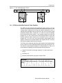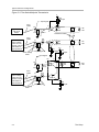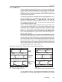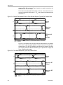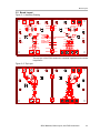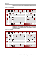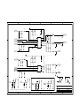
1
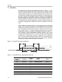
Multipoint-Low Voltage Differential Signaling (M-LVDS) Evaluation Module User’s Guide April 2004 High Performance Analog SLLU039B IMPORTANT NOTICE Texas Instruments Incorporated and its subsidiaries (TI) reserve the right to make corrections, modifications, enhancements, improvements, and other changes to its products and services at any time and to discontinue any product or service without notice. Customers should obtain the latest relevant information before placing orders and should verify that such information is current and complete. All products are sold subject to TI’s terms and conditions of sale supplied at the time of order acknowledgment. TI warrants performance of its hardware products to the specifications applicable at the time of sale in accordance with TI’s standard warranty. Testing and other quality control techniques are used to the extent TI deems necessary to support this warranty. Except where mandated by government requirements, testing of all parameters of each product is not necessarily performed. TI assumes no liability for applications assistance or customer product design. Customers are responsible for their products and applications using TI components. To minimize the risks associated with customer products and applications, customers should provide adequate design and operating safeguards. TI does not warrant or represent that any license, either express or implied, is granted under any TI patent right, copyright, mask work right, or other TI intellectual property right relating to any combination, machine, or process in which TI products or services are used. Information published by TI regarding third-party products or services does not constitute a license from TI to use such products or services or a warranty or endorsement thereof. Use of such information may require a license from a third party under the patents or other intellectual property of the third party, or a license from TI under the patents or other intellectual property of TI. Reproduction of information in TI data books or data sheets is permissible only if reproduction is without alteration and is accompanied by all associated warranties, conditions, limitations, and notices. Reproduction of this information with alteration is an unfair and deceptive business practice. TI is not responsible or liable for such altered documentation. Resale of TI products or services with statements different from or beyond the parameters stated by TI for that product or service voids all express and any implied warranties for the associated TI product or service and is an unfair and deceptive business practice. TI is not responsible or liable for any such statements. Following are URLs where you can obtain information on other Texas Instruments products and application solutions: Products Amplifiers Applications amplifier.ti.com Audio www.ti.com/audio Data Converters dataconverter.ti.com Automotive www.ti.com/automotive DSP dsp.ti.com Broadband www.ti.com/broadband Interface interface.ti.com Digital Control www.ti.com/digitalcontrol Logic logic.ti.com Military www.ti.com/military Power Mgmt power.ti.com Optical Networking www.ti.com/opticalnetwork Microcontrollers microcontroller.ti.com Security www.ti.com/security Mailing Address: Telephony www.ti.com/telephony Video & Imaging www.ti.com/video Wireless www.ti.com/wireless Texas Instruments Post Office Box 655303 Dallas, Texas 75265 Copyright 2004, Texas Instruments Incorporated EVM IMPORTANT NOTICE Texas Instruments (TI) provides the enclosed product(s) under the following conditions: This evaluation kit being sold by TI is intended for use for ENGINEERING DEVELOPMENT OR EVALUATION PURPOSES ONLY and is not considered by TI to be fit for commercial use. As such, the goods being provided may not be complete in terms of required design-, marketing-, and/or manufacturing-related protective considerations, including product safety measures typically found in the end product incorporating the goods. As a prototype, this product does not fall within the scope of the European Union directive on electromagnetic compatibility and therefore may not meet the technical requirements of the directive. Should this evaluation kit not meet the specifications indicated in the EVM User’s Guide, the kit may be returned within 30 days from the date of delivery for a full refund. THE FOREGOING WARRANTY IS THE EXCLUSIVE WARRANTY MADE BY SELLER TO BUYER AND IS IN LIEU OF ALL OTHER WARRANTIES, EXPRESSED, IMPLIED, OR STATUTORY, INCLUDING ANY WARRANTY OF MERCHANTABILITY OR FITNESS FOR ANY PARTICULAR PURPOSE. The user assumes all responsibility and liability for proper and safe handling of the goods. Further, the user indemnifies TI from all claims arising from the handling or use of the goods. Please be aware that the products received may not be regulatory compliant or agency certified (FCC, UL, CE, etc.). Due to the open construction of the product, it is the user’s responsibility to take any and all appropriate precautions with regard to electrostatic discharge. EXCEPT TO THE EXTENT OF THE INDEMNITY SET FORTH ABOVE, NEITHER PARTY SHALL BE LIABLE TO THE OTHER FOR ANY INDIRECT, SPECIAL, INCIDENTAL, OR CONSEQUENTIAL DAMAGES. TI currently deals with a variety of customers for products, and therefore our arrangement with the user is not exclusive. TI assumes no liability for applications assistance, customer product design, software performance, or infringement of patents or services described herein. Please read the EVM User’s Guide and, specifically, the EVM Warnings and Restrictions notice in the EVM User’s Guide prior to handling the product. This notice contains important safety information about temperatures and voltages. For further safety concerns, please contact the TI application engineer. Persons handling the product must have electronics training and observe good laboratory practice standards. No license is granted under any patent right or other intellectual property right of TI covering or relating to any machine, process, or combination in which such TI products or services might be or are used. Mailing Address: Texas Instruments Post Office Box 655303 Dallas, Texas 75265 Copyright 2004, Texas Instruments Incorporated EVM WARNINGS AND RESTRICTIONS It is important to operate this EVM within the supply voltage range of 3 V to 3.6 V. Exceeding the specified supply range may cause unexpected operation and/or irreversible damage to the EVM. If there are questions concerning the supply range, please contact a TI field representative prior to connecting the input power. Applying loads outside of the specified output range may result in unintended operation and/or possible permanent damage to the EVM. Please consult the EVM User’s Guide prior to connecting any load to the EVM output. If there is uncertainty as to the load specification, please contact a TI field representative. During normal operation, some circuit components may have case temperatures greater than 125°C. The EVM is designed to operate properly with certain components above 125°C as long as the input and output ranges are maintained. These components include but are not limited to linear regulators, switching transistors, pass transistors, and current sense resistors. These types of devices can be identified using the EVM schematic located in the EVM User’s Guide. When placing measurement probes near these devices during operation, please be aware that these devices may be very warm to the touch. Mailing Address: Texas Instruments Post Office Box 655303 Dallas, Texas 75265 Copyright 2004, Texas Instruments Incorporated Preface How to Use This Manual This document contains the following chapters: - Chapter 1—The M-LVDS Evaluation Module - Chapter 2—Test Setup - Chapter 3—Bill of Materials, Board Layout, and PCB Construction - Appendix A—Schematic Related Documentation From Texas Instruments and Others - Introduction to M-LVDS (SLLA108) - LVDS Designer’s Notes (SLLA014A). - Reducing EMI With Low Voltage Differential Signaling (SLLA030B). - Interface Circuits for TIA/EIA−644 (LVDS) (SLLA038B). - Transmission at 200 Mpbs in VME Card Cage Using LVDM (SLLA088). - LVDS Multidrop Connections (literature number SLLA054). - SN65MLVD20x data sheets, Multipoint-LVDS Line Drivers and Receivers, (SLLS573 and SLLS558) - Electromagnetic Compatibility Printed Circuit Board and Electronic Module Design, VEC workshop, Violette Engineering Corporation. FCC Warning This equipment is intended for use in a laboratory test environment only. It generates, uses, and can radiate radio frequency energy and has not been tested for compliance with the limits of computing devices pursuant to subpart J of part 15 of FCC rules, which are designed to provide reasonable protection against radio frequency interference. Operation of this equipment in other environments may cause interference with radio communications. In which case the user, at his own expense, is required to take the necessary measures to correct this interference. Read This First v vi Running Title—Attribute Reference Contents 1 The M-LVDS Evaluation Module . . . . . . . . . . . . . . . . . . . . . . . . . . . . . . . . . . . . . . . . . . . . . . . . . . 1.1 Overview . . . . . . . . . . . . . . . . . . . . . . . . . . . . . . . . . . . . . . . . . . . . . . . . . . . . . . . . . . . . . . . . . 1.2 M-LVDS Standard TIA/EIA−899 . . . . . . . . . . . . . . . . . . . . . . . . . . . . . . . . . . . . . . . . . . . . . . 1.3 M-LVDS EVM Kit Contents . . . . . . . . . . . . . . . . . . . . . . . . . . . . . . . . . . . . . . . . . . . . . . . . . . 1.4 Configurations . . . . . . . . . . . . . . . . . . . . . . . . . . . . . . . . . . . . . . . . . . . . . . . . . . . . . . . . . . . . . 1.4.1 Point-to-Point . . . . . . . . . . . . . . . . . . . . . . . . . . . . . . . . . . . . . . . . . . . . . . . . . . . . . . 1.4.2 Multidrop . . . . . . . . . . . . . . . . . . . . . . . . . . . . . . . . . . . . . . . . . . . . . . . . . . . . . . . . . . 1.4.3 Multipoint . . . . . . . . . . . . . . . . . . . . . . . . . . . . . . . . . . . . . . . . . . . . . . . . . . . . . . . . . . 1.4.4 EVM Operation With Separate Power Supplies . . . . . . . . . . . . . . . . . . . . . . . . . . 1.5 Recommended Equipment . . . . . . . . . . . . . . . . . . . . . . . . . . . . . . . . . . . . . . . . . . . . . . . . . . 1-1 1-2 1-3 1-4 1-5 1-5 1-6 1-6 1-7 1-8 2 Test Setup . . . . . . . . . . . . . . . . . . . . . . . . . . . . . . . . . . . . . . . . . . . . . . . . . . . . . . . . . . . . . . . . . . . . . 2.1 Typical Cable Test Configurations . . . . . . . . . . . . . . . . . . . . . . . . . . . . . . . . . . . . . . . . . . . . 2.1.1 Point-to-Point Simplex Transmission . . . . . . . . . . . . . . . . . . . . . . . . . . . . . . . . . . . 2.1.2 Point-to-Point Parallel Terminated Simplex Transmission . . . . . . . . . . . . . . . . . 2.1.3 Two-Node Multipoint Transmission . . . . . . . . . . . . . . . . . . . . . . . . . . . . . . . . . . . . 2.2 Test Results . . . . . . . . . . . . . . . . . . . . . . . . . . . . . . . . . . . . . . . . . . . . . . . . . . . . . . . . . . . . . . . 2-1 2-2 2-2 2-3 2-3 2-5 3 Bill of Materials, Board Layout, and PCB Construction . . . . . . . . . . . . . . . . . . . . . . . . . . . . . 3.1 Bill of Materials . . . . . . . . . . . . . . . . . . . . . . . . . . . . . . . . . . . . . . . . . . . . . . . . . . . . . . . . . . . . 3.2 Board Layout . . . . . . . . . . . . . . . . . . . . . . . . . . . . . . . . . . . . . . . . . . . . . . . . . . . . . . . . . . . . . . 3.3 PCB Construction . . . . . . . . . . . . . . . . . . . . . . . . . . . . . . . . . . . . . . . . . . . . . . . . . . . . . . . . . . 3-1 3-2 3-3 3-6 A Schematic . . . . . . . . . . . . . . . . . . . . . . . . . . . . . . . . . . . . . . . . . . . . . . . . . . . . . . . . . . . . . . . . . . . . . . A-1 Chapter Title—Attribute Reference vii Running Title—Attribute Reference Figures 1−1. 1−2. 1−3 1−4 1−5 1−6 1−7 1−8 2−1 2−2 2−3 2−4 2−5 2−6 3−1 3−2 3−3 3−4 3−5 3−6 M-LVDS Unit Interval Definition . . . . . . . . . . . . . . . . . . . . . . . . . . . . . . . . . . . . . . . . . . . . . . . . . Expanded Graph of Receiver Differential Input Voltage Showing Transition Region . . . . Point-to-Point Simplex Circuit . . . . . . . . . . . . . . . . . . . . . . . . . . . . . . . . . . . . . . . . . . . . . . . . . . Parallel Termination Simplex Circuit . . . . . . . . . . . . . . . . . . . . . . . . . . . . . . . . . . . . . . . . . . . . . Multidrop or Distributed Simplex Circuit . . . . . . . . . . . . . . . . . . . . . . . . . . . . . . . . . . . . . . . . . . Five-Node Multipoint Circuit . . . . . . . . . . . . . . . . . . . . . . . . . . . . . . . . . . . . . . . . . . . . . . . . . . . . Two-Node Multipoint Circuit . . . . . . . . . . . . . . . . . . . . . . . . . . . . . . . . . . . . . . . . . . . . . . . . . . . . EVM Configuration for Including a Ground Potential Difference Voltage Between Nodes Point-to-Point Simplex Transmission . . . . . . . . . . . . . . . . . . . . . . . . . . . . . . . . . . . . . . . . . . . . Point-to-Point Parallel Terminated Simplex Transmission . . . . . . . . . . . . . . . . . . . . . . . . . . . Two-Node Multipoint Transmission . . . . . . . . . . . . . . . . . . . . . . . . . . . . . . . . . . . . . . . . . . . . . . Point-to-Point Parallel Simplex Typical Eye Pattern Data . . . . . . . . . . . . . . . . . . . . . . . . . . . Parallel Terminated Point-to-Point Parallel Simplex Typical Eye Pattern Data . . . . . . . . . . Two-Node Multipoint Typical Eye Pattern Data . . . . . . . . . . . . . . . . . . . . . . . . . . . . . . . . . . . . Assembly Drawing . . . . . . . . . . . . . . . . . . . . . . . . . . . . . . . . . . . . . . . . . . . . . . . . . . . . . . . . . . . . Top Layer . . . . . . . . . . . . . . . . . . . . . . . . . . . . . . . . . . . . . . . . . . . . . . . . . . . . . . . . . . . . . . . . . . . Second Layer . . . . . . . . . . . . . . . . . . . . . . . . . . . . . . . . . . . . . . . . . . . . . . . . . . . . . . . . . . . . . . . . Third Layer . . . . . . . . . . . . . . . . . . . . . . . . . . . . . . . . . . . . . . . . . . . . . . . . . . . . . . . . . . . . . . . . . . Bottom Layer . . . . . . . . . . . . . . . . . . . . . . . . . . . . . . . . . . . . . . . . . . . . . . . . . . . . . . . . . . . . . . . . Trace Configurations in Printed-Circuit Boards . . . . . . . . . . . . . . . . . . . . . . . . . . . . . . . . . . . . 1-2 1-4 1-5 1-5 1-6 1-6 1-7 1-8 2-2 2-3 2-4 2-5 2-6 2-6 3-3 3-3 3-4 3-4 3-5 3-7 Tables 1−1 1−2 2−1 3−1 3−2 viii M−LVDS Devices Supported by the EVM . . . . . . . . . . . . . . . . . . . . . . . . . . . . . . . . . . . . . . . . Receiver Input Voltage Threshold Requirements . . . . . . . . . . . . . . . . . . . . . . . . . . . . . . . . . . EVM Configuration Options . . . . . . . . . . . . . . . . . . . . . . . . . . . . . . . . . . . . . . . . . . . . . . . . . . . . M-LVDS EVM Bill of Materials . . . . . . . . . . . . . . . . . . . . . . . . . . . . . . . . . . . . . . . . . . . . . . . . . . EVM Layer Stack Up . . . . . . . . . . . . . . . . . . . . . . . . . . . . . . . . . . . . . . . . . . . . . . . . . . . . . . . . . . 1-2 1-4 2-2 3-2 3-8 Chapter 1 The M-LVDS Evaluation Module This document describes the multipoint low-voltage differential-signaling (M-LVDS) evaluation module (EVM) used to aid designers in development and analysis of this new signaling technology. The Texas Instruments SN65MLVD200A, SN65MLVD201, SN65MLVD202A, SN65MLVD203, SN65MLVD204A, SN65MLVD205A, SN65MLVD206, SN65MLVD207 series are low-voltage differential line drivers and receivers complying with the M-LVDS standard (TIA/EIA−899). The EVM kit contains the assembled printed-circuit board and all of the released devices referred to in Table 1−1. Using the EVM to evaluate these devices should provide insight into the design of low-voltage differential circuits. The EVM board allows the designer to connect an input to one or both of the drivers and configure a point-to-point, multidrop, or multipoint data bus. The EVM can be used to evaluate device parameters while acting as a guide for high-frequency board layout. The board allows for the connection of a 100-Ω controlled impedance cable of varying lengths. This provides the designer with a tool for evaluation and successful design of an end product. Topic Page 1.1 Overview . . . . . . . . . . . . . . . . . . . . . . . . . . . . . . . . . . . . . . . . . . . . . . . . . . . . . 1-2 1.2 M-LVDS Standard TIA/EIA−899 . . . . . . . . . . . . . . . . . . . . . . . . . . . . . . . . . 1-3 1.3 M-LVDS EVM Kit Contents . . . . . . . . . . . . . . . . . . . . . . . . . . . . . . . . . . . . . 1-4 1.4 Configurations . . . . . . . . . . . . . . . . . . . . . . . . . . . . . . . . . . . . . . . . . . . . . . . . 1-5 1.5 Recommended Equipment . . . . . . . . . . . . . . . . . . . . . . . . . . . . . . . . . . . . . 1-8 The M-LVDS Evaluation Module 1-1 Overview 1.1 Overview The EVM comes with all the production devices in Table 1−1. The SN65MLVD201 and SN65MLVD207 are installed on the circuit board, and can easily be replaced with the other devices supplied. The M-LVDS devices evaluated with this EVM are in the SN75ALS180 and SN75176 footprint. Use of these industry standard footprints allows the designer to easily configure the parts into a simplex or half-duplex data bus. These are all TIA/EIA−899 M-LVDS standard compliant devices. While initially intended for half-duplex or multipoint applications, M-LVDS devices are not precluded from being used in a point-to-point or multidrop configuration. In these configurations there can be a distinct advantage to the additional current drive provided by an M-LVDS driver. The M-LVDS devices shown in Table 1−1 all include output slew-rate limited drivers, thus the need for different nominal signaling rates. The M-LVDS standard recommends the transition time not exceed 0.5 of the unit interval (UI). The definition of transition time (tr and tf) in M-LVDS is the 10% to 90% levels shown in Figure 1−1. Using the maximum transition time for each of the drivers and the 0.5(tUI) rule results in the signaling rates shown in Table 1−1. This slew-rate control differentiates M-LVDS devices from LVDS (TIA/EIA−644A) compliant devices. The slower transition times available with M-LVDS help to reduce higher frequency components in the transmitted signal. This reduces EMI and allows longer stubs on the main transmission line. For this reason it is generally better to select a driver with a specified signaling rate no greater than is required in the system. Figure 1−1. M-LVDS Unit Interval Definition tr tf 90% 50% 10% UI Table 1−1. M-LVDS Devices Supported by the EVM 1-2 Nominal Signaling Rate (Mbps) Footprints Receiver Type Part Number Status 100 SN75176 Type-1 SN65MLVD200AD Production 200 SN75176 Type-1 SN65MLVD201D Production 100 SN75ALS180 Type-1 SN65MLVD202AD Production 200 SN75ALS180 Type-1 SN65MLVD203D Production 100 SN75176 Type-2 SN65MLVD204AD Production 100 SN75ALS180 Type-2 SN65MLVD205AD Production 200 SN75176 Type-2 SN65MLVD206D Production 200 SN75ALS180 Type-2 SN65MLVD207D Production The M-LVDS Evaluation Module M-LVDS Standard TIA/EIA−899 The EVM has been designed with the individual driver and receiver section (SN75ALS180 footprint, U1) on one half of the board and the transceiver section (SN75176 footprint, U2) on the other half (see Figure 3−1). The EVM as delivered incorporates two 100-Ω termination resistors at each driver output, receiver input, and transceiver I/O. These allow the user to evaluate a single driver, receiver, or transceiver, while not having to deal with a transmission line or additional I/Os. Jumpers are included to allow the two sections of the EVM to either share the same power and ground or be run off of independent supplies. Ground shifts or common-mode offsets can be introduced by the removal of these jumpers and using separate power supplies. 1.2 M-LVDS Standard TIA/EIA−899 The M-LVDS standard was created in response to a demand from the data communications community for a general-purpose high-speed balanced interface standard for multipoint applications. The TIA/EIA−644 standard defines the LVDS electrical-layer characteristics used for transmitting information in point-to-point and multidrop architectures. TIA/EIA−644 does not address data transmission for multipoint architectures, therefore the need for development of a new standard. The standard, Electrical Characteristics of Multipoint-Low-Voltage Differential Signaling (M-LVDS) TIA/EIA−899, specifies low-voltage differential signaling drivers and receivers for data interchange across half-duplex or multipoint data bus structures. M-LVDS is capable of operating at signaling rates up to 500 Mbps. In other words, when the devices are used at the nominal signaling rate, the rise and fall times will be within the specified values in the standard. The M-LVDS standard defines the transition time (tr and tf) to be 1 ns or slower into a test load. Using this information combined with the requirement that the transition time not exceed 0.5 of the unit interval (UI), gives a minimum unit interval of 2 ns, leading to the 500 Mpbs maximum signaling rate. The standard defines Type-1 and Type-2 receivers. Type-1 receivers include no provisions for failsafe and have their differential input voltage thresholds near zero volts. Type-2 receivers have their differential input voltage thresholds offset from zero volts to detect the absence of a voltage difference. Type-1 receivers maximize the differential noise margin and are intended for the maximum signaling rate. Type-2 receivers are intended for control signals, slower signaling rates, or where failsafe provisions are needed. The bus voltage logic state definition can be seen in Table 1−2 and Figure 1−2. The M-LVDS Evaluation Module 1-3 M-LVDS EVM Kit Contents Table 1−2. Receiver Input Voltage Threshold Requirements Receiver Type Low High Type-1 −2.4 V ≤ VID ≤ −0.05 V 0.05 V ≤ VID ≤ 2.4 V Type-2 −2.4 V ≤ VID ≤ 0.05 V 0.15 V ≤ VID ≤ 2.4 V Figure 1−2. Expanded Graph of Receiver Differential Input Voltage Showing Transition Region Type−1 and Type−2 Receiver Differential Input Thresholds Type 1 Type 2 2.4 ÎÎÎÎÎÎÎÎÎÎÎÎ ÎÎÎÎÎÎÎÎÎÎÎÎ ÎÎÎÎÎÎÎÎÎÎÎÎ ÎÎÎÎÎÎÎÎÎÎÎÎ ÎÎÎÎÎÎÎÎÎÎÎÎ ÎÎÎÎÎÎÎÎÎÎÎ ÎÎÎÎÎÎÎÎÎÎÎÎ ÎÎÎÎÎÎÎÎÎÎÎ ÎÎÎÎÎÎÎÎÎÎÎ ÎÎÎÎÎÎÎÎÎÎÎ ÎÎÎÎÎÎÎÎÎÎÎ High 0.15 High VID (V) 0.1 0.05 0 Low −0.05 Low −2.4 Transition Region 1.3 M-LVDS EVM Kit Contents The M-LVDS EVM kit contains the following: J M-LVDS EVM PWB with SN65MLVD201D and SN65MLVD207D installed (6424409B) J Additional devices SN65MLVD200A, SN65MLVD202A, SN65MLVD203, SN65MLVD204A, SN65MLVD205A, SN65MLVD206 J M-LVDS EVM kit documentation (user’s guide) J SN65MLVD20x data sheets, Multipoint-LVDS Line Driver and Receiver, (SLLS573 and SLLS558) 1-4 The M-LVDS Evaluation Module Configurations 1.4 Configurations The M-LVDS EVM board allows the user to construct various bus configurations. The two devices on the EVM allow for point-to-point simplex, parallel-terminated point-to-point simplex, and two-node multipoint operation. All of these modes of operation can be configured through onboard jumpers, external cabling, and different resistor combinations. The devices which are delivered with the EVM change output operation but, configuration of jumpers to setup the transmission type is independent of the devices installed 1.4.1 Point-to-Point The point-to-point simplex configuration is shown in Figure 1−3. The setup schematic for this option is shown in Figure 2−1. Although this is not the intended mode of operation for M-LVDS, it works well for high noise or long higher-loss transmission lines. Due to the increased drive current, a single 100-Ω termination resistor on the EVM will result in a differential bus voltage (VOD) twice as large as a doubly terminated line. This practice is acceptable as long as the combination of input voltage and common-mode voltage does not exceed absolute maximum ratings of the line circuits. Figure 1−3. Point-to-Point Simplex Circuit U1 U1 T This configuration can also have a termination at the source and load (parallel terminated), thereby, keeping normal M-LVDS signal levels as shown in Figure 1−4. The schematic for this option is shown in Figure 2−2. Due to the increased drive current, double termination can be used to improve transmission line characteristics . Figure 1−4. Parallel Termination Simplex Circuit U1 U1 T T The M-LVDS Evaluation Module 1-5 Configurations 1.4.2 Multidrop A multidrop configuration (see Figure 1−5) with two receiver nodes can be simulated with the EVM. To get additional receiver nodes on the same bus requires additional EVMs. M-LVDS controlled driver transition times and higher signal levels help to accommodate the multiple stubs and additional loads on the bus. This does not exempt good design practices, which would keep stubs short to help prevent excessive signal reflections. A bus line termination could be placed at both ends of the transmission line, improving the signal quality by reducing return reflections to the driver. This would allow the use of standard compliant TIA/EIA 644A receivers on the bus in addition to M-LVDS receivers. Figure 1−5. Multidrop or Distributed Simplex Circuit T 1.4.3 Multipoint The multipoint configuration is the primary application of the M-LVDS devices and the associated standard. The M-LVDS standard allows for any combination of drivers, receivers, or transceivers up to a total of 32 on the line. Figure 1−6 shows a representation of a five-node multipoint configuration using transceivers. Increased drive current, in addition to the wider commonmode input, allows M-LVDS parts to drive multiple receivers over longer line lengths with up to 2 V of ground noise. Figure 1−6. Five-Node Multipoint Circuit T T A two-node multipoint setup (see Figure 1−7) can be configured with the EVM. Additional EVMs are needed for more nodes. The test setup and schematic for this configuration is shown in Figure 2−3. 1-6 The M-LVDS Evaluation Module Configurations Figure 1−7. Two-Node Multipoint Circuit T T U2 U1 1.4.4 EVM Operation With Separate Power Supplies The EVM has been designed with independent power planes for the two devices. The two devices can be powered with independent supplies or with a single supply. Sending and receiving data between backplanes, racks, or cabinets where separate power sources may exist can have offset ground potentials between nodes. Jumpers W7, 8, 9, and 10 tie the two separate power and ground planes together. If two separate supplies are used and jumpers W7, 8, 9, and 10 are removed, care should be taken to ensure the absolute maximum device ratings are not exceeded. Keep in mind that if jumpers W7, 8, 9, and 10 are not removed when using separate power supplies, a difference in potential between the supplies causes a current to flow between supplies and through the jumpers. The EVM can be configured with three power supplies with isolated outputs in such a way as to input a fixed offset between the grounds (see Figure 1−8). This induces a ground potential difference voltage between U1 and U2. To demonstrate this capability, the following steps should be followed. - Adjust PS1 and PS3 to the supply voltage (3.3 V) and current limit to 50 mA. - Set PS2 to 0 V - Induce a ground offset by varying the output of PS2. PS2 Output The PS2 output should not exceed ± 2 V to remain within the device ratings. The M-LVDS Evaluation Module 1-7 Recommended Equipment Figure 1−8. EVM Configuration for Including a Ground Potential Difference Voltage Between Nodes + PS1 − J13 J14 + W10 W8 W7 W9 PS2 J17 − J18 + PS3 Jumpers removed from W7, W8, W9, W10 − 1.5 Recommended Equipment - 3.3 Vdc at 0.5-A power supply or multiple power supplies (with both devices powered and enabled the board draws about 35 mA). - A 100-Ω transmission medium from the driver to the receiver, (twisted-pair cable recommended, CAT5 cable for example). - A function or pattern generator capable of supplying 3.3-V signals at the desired signaling rate. - A multiple-channel high-bandwidth oscilloscope, preferably above the 1-GHz range - Differential or single ended oscilloscope probes. 1-8 The M-LVDS Evaluation Module Chapter 2 Test Setup This chapter describes how to setup and use the M-LVDS EVM. Topic Page 2.1 Typical Cable Test Configurations . . . . . . . . . . . . . . . . . . . . . . . . . . . . . . 2-2 2.2 Test Results . . . . . . . . . . . . . . . . . . . . . . . . . . . . . . . . . . . . . . . . . . . . . . . . . . 2-5 Test Setup 2-1 Typical Cable Test Configurations 2.1 Typical Cable Test Configurations Each of the following test configurations is a transmission line consisting of a twisted-pair cable connected on the 2-pin connectors (P1, P2, or P3). Table 2−1 shows the possible configurations. In addition to the different transmission topologies, the EVM can also be configured to run off two or three separate power supplies, as described in the previous section. This would allow the user to induce a ground shift or offset between the two different drivers and receivers. This setup can be used with any transmission line test. Table 2−1. EVM Configuration Options Configuration Jumpers In Resistors In Resistors Out Diagram Point-to-point simplex transmission W1, 2, 7, 8, 9, 10 R4 R5, 6, 7 Figure 2−1 Point-to-point parallel terminated simplex transmission W1, 2, 7, 8, 9, 10 R4, 7 R5, 6 Figure 2−2 Two-node multipoint transmission W1, 2, 3, 4, 7, 8, 9, 10 R5, 16 R2, 4, 6, 7, 13 15 Figure 2−3 2.1.1 Point-to-Point Simplex Transmission 1) Connect a twisted-pair cable from P1 to P2. 2) Verify resistor R4 is installed. 3) Remove resistors R5, R6, and R7. This properly terminates the transmission line at one end. 4) Enable the driver by connecting the jumper on W2 between pin 1 and pin 2, or U1 pin 4 to VCC. 5) Enable the receiver by connecting the jumper on W1 between pin 2 and pin 3, or U1 pin 3 to GND. Figure 2−1. Point-to-Point Simplex Transmission VCC Jumper W2 Input Signal 50- Ω Cable Signal Source with 50-Ω Output 5 50-Ω Cable Active Voltage Probe J1 R2 453 TP1 Output Signal 9 U1 10 R3 49.9 TP2 50- Ω cable or Active Voltage Probe into one Channel of Scope Terminated in High Impedance 2-2 4 J2 R7 100 P2 R6 100 Twisted Pair Cable 2 12 U1 3 11 VCC R4 100 P1 R5 100 W1 Jumper Test Setup Typical Cable Test Configurations 2.1.2 Point-to-Point Parallel Terminated Simplex Transmission 1) Connect a twisted-pair cable from P1 to P2. 2) Verify resistor R4 and R7 are installed. 3) Remove resistors R5 and R6. This properly terminates the transmission line at both ends. 4) Enable the driver by connecting the jumper on W2 between pin 1 and pin 2, or U1 pin 4 to VCC. 5) Enable the receiver by connecting the jumper on W1 between pin 2 and pin 3, or U1 pin 3 to GND. Figure 2−2. Point-to-Point Parallel Terminated Simplex Transmission VCC Jumper W2 Input Signal 50-Ω Cable Signal Source with 50-Ω Output 5 50-Ω Cable J1 R2 453 TP1 Active Voltage Probe 9 U1 10 R3 49.9 TP2 50- Ω cable or Active Voltage Probe into one Channel of Scope Terminated in High Impedance 2.1.3 4 J2 R7 100 R6 100 P2 Twisted Pair Cable 2 12 U1 3 11 VCC Output Signal R4 100 P1 R5 100 W1 Jumper Two-Node Multipoint Transmission 1) Connect a twisted-pair cable between P1, P2, and P3. 2) Verify resistor R5 and R16 are installed. 3) Remove resistors R4, R6, R7, and R15. This properly terminates the transmission line at both ends. 4) Enabling the driver in a two-node multipoint configuration will be a slightly more challenging task. The user can either jumper enable a single driver and send all of the data on the bus through a single driver, or sync the driver enable to the data and send data from each driver. Enable a single driver by connecting the jumper on W4 between pin 1 and pin 2 which connects U2 pin 3 to VCC, or by connecting the jumper on W2 between pin 1 and pin 2 which connects U1 pin 4 to VCC. 5) Enable the receivers by connecting the jumpers on W1 and W3 between pin 2 and pin 3, or U1 pin 3 to GND and U2 pin 2 to GND. Test Setup 2-3 Typical Cable Test Configurations Figure 2−3. Two-Node Multipoint Transmission VCC W2 Jumper Input Signal 50-Ω Cable Signal Source with 50-Ω Output 4 J2 5 R3 49.9 TP2 50- Ω cable or Active Voltage Probe into one Channel of Scope Terminated in High Impedance 50-Ω Cable J1 R7 100 10 P2 R6 100 P1 R5 100 Twisted Pair Cable R2 453 2 12 R4 100 U1 3 TP1 Active Voltage Probe 9 U1 11 VCC W1 Jumper Output Signal VCC W4 Jumper Input Signal 3 U2 J8 4 50- Ω cable or Active Voltage Probe into one Channel of Scope Terminated in High Impedance R15 100 P3 R16 100 R13 453 1 TP3 VCC 2 Active Voltage Probe 2-4 J7 7 R14 49.9 TP4 50-Ω Cable 6 Output Signal W3 Jumper Test Setup Test Results 2.2 Test Results The test configurations described in Section 2.1 were used to simulate pointto-point simplex, parallel-terminated point-to-point simplex, and two-node multipoint. The test results are shown in the following figures. A Tektronix HFS9003 was used to generate input signals, and a Tektronix TDS784D was used to collect the output data. The EVM was populated with a SN65MLVD207D and SN65MLVD201D for U1 and U2 respectively. The eye patterns were measured with the source (Tektronix HFS9003) generating 215−1 PRBS NRZ data. In all cases, the length of the transmission line is approximately 21 inches (53 cm), and adds to the propagation delay in the device. This can be seen in the figures below as a time delay from input to output Figure 2−4 shows the point-to-point simplex transmission eye patterns. Trace 1 is the driver input signal applied to J2. The output signal is shown below measured on both J1 (Figure 2−4 left picture), and TP1 (Figure 2−4 right picture). The receiver output in both figures shows the offset zero crossing, which is due to the Type-2 receiver incorporated into the SN65MLVD207 device. The reduced offset from a Type-1 receiver can be seen in Figure 2−6, receiver number 2 output. Measuring the output signal on J1 with a 50-Ω cable terminated into 50-Ω at the scope will attenuate the signal due to the 453-Ω resistor in series with the receiver output. The resistor is installed as a current limit for termination into a 50-Ω load. As can be seen in the traces below the magnitude of trace 2 on the left is one-tenth of trace 2 on the right. Measuring the signal with a high-impedance probe on TP1 requires replacing R2, the 453-Ω resistor, with a short to reduce signal roll-off. Measuring the output on TP1 allows the user to see absolute signal levels out of the device. Figure 2−4. Point-to-Point Parallel Simplex Typical Eye Pattern Data Driver Input Receiver Output Differential Bus Voltage 50-Ohm Output Termination Receiver Output Scaled 10:1 High Impedance Output Termination, R2 Shorted The eye patterns in Figure 2−5 are parallel-terminated point-to-point simplex data where trace 1 is the input signal applied to J2, and trace 2 is the output Test Setup 2-5 Test Results signal on TP1, R2 is shorted. Type-2 behavior is again observed on the SN65MLVD207 receiver output. Trace three shows the differential voltage on the bus. Note that the bus voltages are nominal M-LVDS levels of 1.1 VPP due to the lower load seen by the current driver. Figure 2−5. Parallel Terminated Point-to-Point Parallel Simplex Typical Eye Pattern Data Driver Input Receiver Output Differential Bus Voltage Figure 2−6 represents the two-node multipoint transmission eye patterns where trace 1 is the input signal applied to J2, and traces 2 and 3 are the output signals seen at TP1 and TP3 respectively with R2 and R13 shorted. The offset zero-crossing shows the difference between Type−2 (Receiver #1 Output) and Type−1 (Receiver #2 Output). Figure 2−6. Two-Node Multipoint Typical Eye Pattern Data Driver Input Receiver #1 Output Receiver #2 Output 2-6 Test Setup Chapter 3 Bill of Materials, Board Layout, and PCB Construction This chapter contains the bill of materials, board layout of the M-LVDS, and describes the printed-circuit board. Topic Page 2.1 Bill of Materials . . . . . . . . . . . . . . . . . . . . . . . . . . . . . . . . . . . . . . . . . . . . . . . 3-2 3.2 Board Layout . . . . . . . . . . . . . . . . . . . . . . . . . . . . . . . . . . . . . . . . . . . . . . . . . 3-3 3.3 PCB Construction . . . . . . . . . . . . . . . . . . . . . . . . . . . . . . . . . . . . . . . . . . . . . 3-6 Bill of Materials, Board Layout, and PCB Construction 3-1 Bill of Materials 3.1 Bill of Materials Table 3−1. M-LVDS EVM Bill of Materials Item No. Qty. 1 2 C1, C2 Capacitor, SMT1206, 50 V, 10%, 0.01 µF AVX 12101C103JATMA 2 4 C5, C6, C9, C10 Capacitor, SMT1206, 16 V, 10%, 1 µF AVX 1206YC105KAT 3 4 C3, C4, C7, C8 Capacitor, SMT1210, 10 V, 10%, 10 µF AVX 1210ZG106ZAT2A 4 2 J11, J13, J15, J17 Banana jack, red Allied ST−351A J11, J15 5 2 J12, J14, J16, J18 Banana jack, black Allied ST−351B J12, J16 6 4 J1 − J 10 Connector Allied 713−4339 J3 − J6, J9, J10 7 4 TP1 − TP4 Header (make from 4−103239−0) AMP 4−103239−0x2 8 3 P1 − P3 Header (make from 4−103239−0) AMP 4−103239−0x2 9 4 W7 − W10 Header (make from 4−103239−0) AMP 4−103239−0x2 10 4 W1 − W4 Header (make from 4−103239−0) AMP 4−103239−0x3 11 1 U1 IC, SMT, 14P, High speed 50-Ω line driver/receiver TI †SN65MLVD202AD IC, SMT, 8P High speed 50-Ω line driver/receiver TI 12 † 1 Reference Designation U2 Description MFG Part # Not Installed SN65MLVD205AD SN65MLVD203D SN65MLVD207D †SN65MLVD200AD SN65MLVD204AD SN65MLVD201D SN65MLVD206D 13 2 R1, R3, R12, R14 Resistor, SMT, 1/4 W, 1%, 49.9 Ω Dale CRCW121049R9F 14 2 R2, R13 Resistor, SMT, 1/4 W, 1%, 453 Ω Dale CRCW12104530F 15 6 R8 − R11, R17, R18 Resistor, SMT, 1/4 W, 1%, 0.0 Ω Dale CRCW12100000F 16 6 R4 − R7, R15, R16 Resistor, SMT, 1/4 W, 1%, 100 Ω Dale CRCW12101000F 17 4 1/2” nylon, hex, standoff Keystone 1902C 18 4 Phillips, pan head, screw 19 8 Jumper, shorting R1, R12 R8 − R11, R17, R18 H703−ND Only one will be installed. 3-2 Bill of Materials, Board Layout, and PCB Construction Board Layout 3.2 Board Layout Figure 3−1. Assembly Drawing J8 J7 J18 R12 TP4W4 W3 VCC01 J15 GND01 VCC01 R14 J16 GND01 TP3 VCC01 GND01 VCC01 J14 W10GND GND VCC W8 J1 J2 J13 VCC R1 W2 W1 TP1 VCC TP2 R2 VCC J12 R4 P1 R5 GND R8 R10 R3 R13 MADE IN U2 U.S.A. TEXAS INSTRUMENTS U1 A/W NO. # 6424409B R15 R7 PWA. EVM. P3 P2 SN65MLVD SERIAL NO. R6 R16 R11 R17 W7 J9 VCC01 VCC J6 J5 GND GND01 W9 J11 GND R9 R18 J10 GND01 J17 J4 J3 The top layer of the EVM contains the controlled impedance and matched length traces. Figure 3−2. Top Layer Bill of Materials, Board Layout, and PCB Construction 3-3 Board Layout The second layer of the EVM has the separate ground planes. These are the reference planes for the controlled impedance traces on the top layer. Figure 3−3. Second Layer ÏÏÏÏÏÏÏÏÏÏÏÏÏÏÏ ÌÌÌÌÌÌÌÌÌÌÌÌÌÌÌ ÏÏÏÏÏÏÏÏÏÏÏÏÏÏÏ ÌÌÌÌÌÌÌÌÌÌÌÌÌÌÌ ÏÏÏÏÏÏÏÏÏÏÏÏÏÏÏ ÌÌÌÌÌÌÌÌÌÌÌÌÌÌÌ ÏÏÏÏÏÏÏÏÏÏÏÏÏÏÏ ÌÌÌÌÌÌÌÌÌÌÌÌÌÌÌ ÏÏÏÏÏÏÏÏÏÏÏÏÏÏÏ ÌÌÌÌÌÌÌÌÌÌÌÌÌÌÌ ÏÏÏÏÏÏÏÏÏÏÏÏÏÏÏ ÌÌÌÌÌÌÌÌÌÌÌÌÌÌÌ ÏÏÏÏÏÏÏÏÏÏÏÏÏÏÏ ÌÌÌÌÌÌÌÌÌÌÌÌÌÌÌ ÏÏÏÏÏÏÏÏÏÏÏÏÏÏÏ ÌÌÌÌÌÌÌÌÌÌÌÌÌÌÌ ÏÏÏÏÏÏÏÏÏÏÏÏÏÏÏ ÌÌÌÌÌÌÌÌÌÌÌÌÌÌÌ ÏÏÏÏÏÏÏÏÏÏÏÏÏÏÏ ÌÌÌÌÌÌÌÌÌÌÌÌÌÌÌ ÏÏÏÏÏÏÏÏÏÏÏÏÏÏÏ ÌÌÌÌÌÌÌÌÌÌÌÌÌÌÌ ÏÏÏÏÏÏÏÏÏÏÏÏÏÏÏ ÌÌÌÌÌÌÌÌÌÌÌÌÌÌÌ ÏÏÏÏÏÏÏÏÏÏÏÏÏÏÏ ÌÌÌÌÌÌÌÌÌÌÌÌÌÌÌ ÏÏÏÏÏÏÏÏÏÏÏÏÏÏÏ ÌÌÌÌÌÌÌÌÌÌÌÌÌÌÌ ÏÏÏÏÏÏÏÏÏÏÏÏÏÏÏ ÌÌÌÌÌÌÌÌÌÌÌÌÌÌÌ The third layer of the EVM has the power planes. These are matched to the ground planes to reduce radiated emission and crosstalk, while increasing distributed capacitance. ÏÏÏÏÏÏÏÏÏÏÏÏÏÏÏ ÌÌÌÌÌÌÌÌÌÌÌÌÌÌÌ ÏÏÏÏÏÏÏÏÏÏÏÏÏÏÏ ÌÌÌÌÌÌÌÌÌÌÌÌÌÌÌ ÏÏÏÏÏÏÏÏÏÏÏÏÏÏÏ ÌÌÌÌÌÌÌÌÌÌÌÌÌÌÌ ÏÏÏÏÏÏÏÏÏÏÏÏÏÏÏ ÌÌÌÌÌÌÌÌÌÌÌÌÌÌÌ ÏÏÏÏÏÏÏÏÏÏÏÏÏÏÏ ÌÌÌÌÌÌÌÌÌÌÌÌÌÌÌ ÏÏÏÏÏÏÏÏÏÏÏÏÏÏÏ ÌÌÌÌÌÌÌÌÌÌÌÌÌÌÌ ÏÏÏÏÏÏÏÏÏÏÏÏÏÏÏ ÌÌÌÌÌÌÌÌÌÌÌÌÌÌÌ ÏÏÏÏÏÏÏÏÏÏÏÏÏÏÏ ÌÌÌÌÌÌÌÌÌÌÌÌÌÌÌ ÏÏÏÏÏÏÏÏÏÏÏÏÏÏÏ ÌÌÌÌÌÌÌÌÌÌÌÌÌÌÌ ÏÏÏÏÏÏÏÏÏÏÏÏÏÏÏ ÌÌÌÌÌÌÌÌÌÌÌÌÌÌÌ ÏÏÏÏÏÏÏÏÏÏÏÏÏÏÏ ÌÌÌÌÌÌÌÌÌÌÌÌÌÌÌ ÏÏÏÏÏÏÏÏÏÏÏÏÏÏÏ ÌÌÌÌÌÌÌÌÌÌÌÌÌÌÌ ÏÏÏÏÏÏÏÏÏÏÏÏÏÏÏ ÌÌÌÌÌÌÌÌÌÌÌÌÌÌÌ ÏÏÏÏÏÏÏÏÏÏÏÏÏÏÏ ÌÌÌÌÌÌÌÌÌÌÌÌÌÌÌ ÏÏÏÏÏÏÏÏÏÏÏÏÏÏÏ ÌÌÌÌÌÌÌÌÌÌÌÌÌÌÌ Figure 3−4. Third Layer 3-4 Bill of Materials, Board Layout, and PCB Construction Board Layout The bottom layer of the EVM contains bulk and decoupling capacitors to be placed close to the power and ground pins on the device. Figure 3−5. Bottom Layer C9 C10 C8 C7 VCC01 C5 C4 GND01 VCC C2 C1 C6 C3 GND Bill of Materials, Board Layout, and PCB Construction 3-5 PCB Construction 3.3 PCB Construction Information in this section was obtained from the following source: - Electromagnetic Compatibility Printed Circuit Board and Electronic Module Design, VEC workshop, Violette Engineering Corporation. Characteristic impedance is the ratio of voltage to current in a transmission line wave traveling in one direction. This characteristic impedance is the value that is matched with our termination resistors so as to reduce reflections. This reduction in reflections improves signal to noise ratio on the line and reduces EMI caused by common mode voltages and spikes. Two typical approaches are used for controlled impedance in printed-circuit board construction, microstrip and stripline. Microstrip construction is shown in Figure 3−6. The characteristic impedance of a microstrip trace on a printed-circuit board is approximated by: ZO + 60 Ǹ0.475år ) 0.67 ln 4h 0.67(0.8 W ) t) (1) where εr is the permeability of the board material, h is the distance between the ground plane and the signal trace, W is the trace width, and t is the thickness of the trace. The differential impedance for a two microstrip traces can be approximated as follows with S being the distance between two microstrip traces: Z DIFF + 2 ZO ǒ1 * 0.48e*0.96sńhǓ (2) Stripline construction is also shown in Figure 3−6, the signal lines should be centered between the ground planes. The characteristic impedance of a stripline trace in a printed-circuit board is approximated by: Z O + 60 Ǹår ln 4h 0.67p(0.8 W ) t) (3) where εr is the permeability of the board material, h is the distance between the ground plane and the signal trace, W is the trace width, and t is the thickness of the trace. The differential impedance for a two stripline traces can be approximated as follows with S being the distance between two stripline traces: Z DIFF + 2 Note: 3-6 ZO ǒ1 * 0.374e*2.9sńhǓ (4) For edge-coupled striplines, the term 0.374 may be replaced with 0.748 for lines which are closely coupled (S < 12 mils, or 0,3 mm). Bill of Materials, Board Layout, and PCB Construction PCB Construction Figure 3−6. Trace Configurations in Printed-Circuit Boards W t W Board Material h MICROSTRIP S W t STRIPLINE Stripline construction is the preferred configuration for differential signaling. This configuration reduces radiated emissions from circuit board traces due to better control of the lines of flux. The additional ground plane also allows for better control of impedance on the traces. It can be seen from the functions and physical construction parameters that careful consideration must be given to these parameters for a robust board design. For instance it is not uncommon for εr to vary 10% across one board, affecting skew. This is a good reason to keep differential lines close. Other factors to keep in mind when doing a printed-circuit layout for transmission lines are as follows: 1) Differences in electrical length translate into skew. 2) Careful attention to dimensions, length and spacing help to insure isolation between differential pairs. 3) Where possible use ideal interconnects, point-to-point with no loads or branches. This keeps the impedance more uniform from end to end and reduce reflections on the line. 4) Discontinuities on the line, vias, pads, test points will: J Reduce characteristic impedance J Increase the prop delay, and rise-time degradation J Increase signal transition time 5) Prioritize signals and avoid turns in critical signals. Turns can cause impedance discontinuities. 6) Within a pair of traces, the distance between the traces should be minimized to maintain common-mode rejection of the receivers. Differential transmission works best when both lines of the pair are kept as identical as possible. Bill of Materials, Board Layout, and PCB Construction 3-7 PCB Construction Table 3−2 shows the layer stack up of the EVM with the defined trace widths for the controlled impedance etch runs using microstrip construction. Table 3−2. EVM Layer Stack Up Differential Model Material Type: FR 406 Layer No. Layer Type Thickness (mils) Copper Weight Line Width (mils) Spacing (mils) Impedance (Ω) Line Width (mils) Impedance (Ω) 1 Signal 0.0006 0.5 oz (start) 0.027 0.230 100 0.0420 50 0.027 0.230 100 0.0420 50 PREPREG 0.025 2 Plane CORE 0.0012 1 0.004 3 Plane PREPREG 0.0012 1 0.025 4 3-8 Single-Ended Model Signal 0.0006 0.5 oz (start) Bill of Materials, Board Layout, and PCB Construction Appendix A Schematic This Appendix contains the EVM schematic. Schematic A-1 1 2 3 4 5 6 V CC R2 453 W1 ReceiverO utput D W2 C1 0.01uF J1 R1* 49.9 D R8* 0.0 TP1 J3* ReceiverInput+ U1 1 2 ReceiverEnable 3 D riverEnable 4 5 D riverInput J2 5 R3 49.9 TP2 7 NC V cc R V cc RE A DE B D Z GND Y GND NC 14 R4 100 13 P1 R5 100 12 R9* 0.0 J4* 11 RecieverInputJ5* 10 D riverO utputR10* 0.0 9 8 R7 100 SN 65M LV D 202,203,205,O R 207 P2 R6 100 C R11* 0.0 C J6* GND D riverO utput+ V CC01 W3 R13 453 W4 C2 0.01uF ReceiverO utput J7 R12* 49.9 TP3 R17* 0.0 J9* TransceiverI/O U2 1 B 2 ReceiverEnable 3 D riverEnable 4 D riverInput J8 R V cc RE B DE A D GND 8 B 7 R15 100 6 P3 R16 100 5 R18* 0.0 SN 65M LV D 200,201,204 OR 206 R14 49.9 J10* TransceiverI/O TP4 V CC J13 J14 J17 V CC J18 V CC01 J11* J12* J15* V CC V cc W8 W9 W 10 V CC01 V cc01 V cc A W7 J16* V CC01 C7 10uF C10 1.0uF C8 10uF V cc01 C9 1uF A C3 10uF C6 1.0uF C4 10uF C5 1uF Title M -LVDS EVM SCHEM ATIC Size O PTIO N AL B * These partsare forboard testpurposesonly and notinstalled in the finalproduct. D ate: File: 1 2 3 4 5 N um ber Revision 6424409 27-Feb-2002 Sheet of C:\Userdata\Protel_database\LV D M 200_EVDMraw .ddb n By: Loren D em ers 6