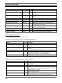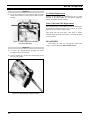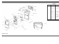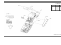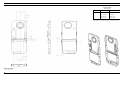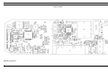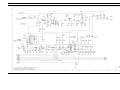
1
Maintenance Manual Prism HP / LPE-200 SCAN And SYSTEM PORTABLE RADIOS 800 MHz tab ericssonz AE/LZB 119 1641 R1B MANUAL REVISION HISTORY REVISION R1A R1B DATE OCT 1995 JUL 1996 REASON FOR CHANGE Original issue Add LPE-200 info. Correct Assembly Diagrams and Parts List NOTICE! This manual covers Ericsson and General Electric products manufactured and sold by Ericsson Inc. NOTICE! Repairs to this equipment should be made only by an authorized service technician or facility designated by the supplier. Any repairs, alterations or substitution of recommended parts made by the user to this equipment not approved by the manufacturer could void the user’s authority to operate the equipment in addition to the manufacturer’s warranty. NOTICE! The software contained in this device is copyrighted by Ericsson Inc. Unpublished rights are reserved under the copyright laws of the United States. This manual is published by Ericsson Inc., without any warranty. Improvements and changes to this manual necessitated by typographical errors, inaccuracies of current information, or improvements to programs and/or equipment, may be made by Ericsson Inc., at any time and without notice. Such changes will be incorporated into new editions of this manual. No part of this manual may be reproduced or transmitted in any form or by any means, electronic or mechanical, including photocopying and recording, for any purpose, without the express written permission of Ericsson Inc. Copyright October 1995, Ericsson Inc 2 AE/LZB 119 1641 R1B TABLE OF CONTENTS SPECIFICATIONS......................................................................................................................................................................4 GENERAL...............................................................................................................................................................................4 DIGITAL .................................................................................................................................................................................5 RECEIVE ................................................................................................................................................................................5 TRANSMIT.............................................................................................................................................................................5 DESCRIPTION ...........................................................................................................................................................................6 MECHANICAL .......................................................................................................................................................................7 OPTIONS AND ACCESSORIES................................................................................................................................................7 OPERATION...............................................................................................................................................................................8 CONTROLS ............................................................................................................................................................................8 KEYPAD SCAN/SYSTEM FUNCTIONS..............................................................................................................................9 CIRCUIT ANALYSIS...............................................................................................................................................................10 SOFTWARE..........................................................................................................................................................................10 RECEIVER............................................................................................................................................................................10 RX Front End.....................................................................................................................................................................10 Rx Back End ......................................................................................................................................................................11 TRANSMITTER ...................................................................................................................................................................13 Transmit Frequency Generation.........................................................................................................................................13 TX/Converter/Modulator (N150).......................................................................................................................................13 Transmit Band Pass Filter ..................................................................................................................................................14 Buffer Amplifier (V104)....................................................................................................................................................14 Power Amplifier (N101) ....................................................................................................................................................14 Directional Coupler (W100) ..............................................................................................................................................14 Power Sensor Circuit (N102-A).........................................................................................................................................14 Power Control Buffer (N102-B) ........................................................................................................................................15 Transmit Low-Pass Filter/Antenna Switch.........................................................................................................................15 Transmit Modulation .........................................................................................................................................................15 SYNTHESIZER.....................................................................................................................................................................15 Dual Synthesizers (N203/N204) ........................................................................................................................................15 Bilateral Switch (N201) .....................................................................................................................................................16 Main Voltage Controlled Oscillator (U200) ......................................................................................................................16 Main Synthesizer (N203) ...................................................................................................................................................16 Auxiliary Synthesizer (N204) ............................................................................................................................................16 Reference Oscillator (U201) ..............................................................................................................................................16 DC POWER DISTRIBUTION ..............................................................................................................................................16 Synthesizer Regulator (N290)............................................................................................................................................16 Receiver Regulator (N490) ................................................................................................................................................16 Transmit Regulator (N190)................................................................................................................................................17 Tx Switch (V192) ..............................................................................................................................................................17 B+ Switch (V191)..............................................................................................................................................................17 Analog Regulator (N900)...................................................................................................................................................17 +5V-D Switching Regulator (N902) ..................................................................................................................................17 LCD NEGATIVE BIAS GENERATOR ...............................................................................................................................18 SERVICE...................................................................................................................................................................................18 EQUIPMENT REQUIRED ...................................................................................................................................................18 PROGRAMMING .................................................................................................................................................................18 Personality Programming...................................................................................................................................................18 Flash Programming ............................................................................................................................................................19 Programming Mode ...........................................................................................................................................................19 BASIC TROUBLESHOOTING ............................................................................................................................................19 3 AE/LZB 119 1641 R1B TABLE OF CONTENTS (Con’t) INTRODUCTION ERROR CODES .....................................................................................................................................22 Error Code Overview.........................................................................................................................................................22 Error Code Format .............................................................................................................................................................22 Fatal Errors ........................................................................................................................................................................22 Non-Fatal Errors ...............................................................................................................................................................23 Special Error Codes ..........................................................................................................................................................23 ERROR CODES - SPECIFIC................................................................................................................................................23 Hardware Fatal System Error ............................................................................................................................................23 Operational Software Fatal System Errors ........................................................................................................................24 Operational Software Non Fatal System Errors ................................................................................................................25 Radio Programming Errors ................................................................................................................................................26 DISASSEMBLY PROCEDURE ...............................................................................................................................................28 PA Module Replacement ...................................................................................................................................................30 Filters Z400 And Z401 Replacement .................................................................................................................................30 REASSEMBLY .....................................................................................................................................................................30 ASSEMBLY DIAGRAMS AND PARTS LIST........................................................................................................................31 OUTLINE DIAGRAM ..............................................................................................................................................................38 SCHEMATIC DIAGRAMS ......................................................................................................................................................40 SPECIFICATIONS* GENERAL FCC Identification Number DOC Certification Number AXATR-336-A 287-194-340NA Input Voltage 7.5 Vdc (nominal) Frequency Range: Transmit Receive * 806 - 824 MHz 851 - 869 MHz 851 - 869 MHz Frequency Stability ±1.5 PPM Dimensions (Typical)H x W x D: Less knobs and antenna with High Capacity Battery with Extra High Capacity Battery 144 mm x 67 mm x 43 mm 157 mm x 67 mm x 43 mm Weight: with High Capacity Battery with Extra High Capacity Battery 20.8 oz. (589 g) 22.0 oz. (624g) Operable Temperature Range -30°C to +60°C (-22°F to +140°F) * The following models operate 807.5 - 824 Mhz (Limited bandsplit): KRD 103 103/A11, A12, A21, A22 4 Continued AE/LZB 119 1641 R1B SPECIFICATIONS∗ (Con't) DIGITAL AEGIS: Vocoding Method Data Rate Error Corr. Eff: Cryptographic (Optional): Encryption Tech: Key Permutations: Key Storage: Adaptive Multiband Encoding 9600 BPS 8.3 dB at 5% BER Non Linear/Block Transformation 1.8 x 10¹⁹ VGE Algorithm 7.2 x 10¹⁶ DES Algorithm 8 banks of 7 keys RECEIVE Channel Spacing 25/12.5 kHz (NPSPAC) Sensitivity (12 dB SINAD) 0.28 µV Spurious and Image Rejection -70 dB Selectivity: @ 12.5 kHz NPSPAC @ 25 kHz -20 dB -72 dB Intermodulation -72 dB Frequency Separation Full Bandwidth Audio Output 500 mW @ 3% Maximum Distortion TRANSMIT RF Power Output 0.5 - 3 Watts (Normal Trunked) Spurious and Harmonics Meets FCC/DOC Limits (-16 dBm) Modulation/Deviation ±5 kHz Frequency Separation Full Bandwidth FM Hum & Noise (Companion Receiver) -40 dB Audio Distortion Less than 3% @ 1000 Hz, 3 kHz deviation Frequency Stability (-30°C to +60°C: + 25 Ref) ±1.5 PPM Audio Frequency Response EIA ∗ These specifications are intended primarily for the use of the service technician. See the appropriate Specification Sheet for the complete specifications. 5 AE/LZB 119 1641 R1B DESCRIPTION The Ericsson Inc. Prism HP and LPE-200 Portable Radios are rugged, high-quality, high-performance FM twoway communications unit designed to operate in either ANALOG or DIGITAL environments. It is available in either Scan or System versions. These are Ericsson’s smallest and most sophisticated high-specification portable radios, designed to meet worldwide requirements. They utilize custom designed integrated circuits to set new standards for size and weight for a high power, high specification two way radio. These radios are synthesized and can be programmed to operate on both EDACS trunked or conventional communications systems. The Prism HP is the first land mobile terminal product capable of being upgraded for Time Division Multiple Access (TDMA) operation. Features include: • • • • Field Upgradability (Prism HP only) Upgradeable to TDMA in the field through FLASH software and a plug-in DSP module, provides an easy, inexpensive evolution path to TDMA operation as future capacity requirements dictate. Also, conventional only radios can be upgraded to EDACS or AEGIS and optional features such as Prosound can be added. Compact Size Designed small and light with rounded edges to fit comfortably in your hand, while providing specifications and performance superior to larger, heavier radios. Light Weight, Rugged Constructions Features a molded case made of a polycarbonate blend surrounding a metal casting. This construction provides a lightweight yet durable housing designed to withstand years of rugged use. High System/Group Capacity Both the Scan and the System versions can manage up to 800 different EDACS system/group combinations with up to 300 conventional channels. EDACS systems/groups can be configured in many different ways to meet specific user needs. • Dual Mode Capability Conventional operation by simply selecting a preprogrammed conventional system. • Transmit Indicator A red LED indicator on the top of the radio indicates when the radio is transmitting. 6 • Display System and group information, status icons and menu operation is supported by the 3-line, 12-character, alphanumeric back lit Liquid Crystal Display (LCD). • Top-Mounted Rotary Knobs The rugged rotary knobs are designed for ease of operation by allowing tactile access to groups, systems, conventional channels, as well as volume and power control. Knobs are designed with metal protective sleeves which help prevent bent and broken knobs due to impact. • Keypad The back lit keypad allows the user to access the many radio functions. The 6-button SCAN provides easy access to preprogrammed telephone and individual radio ID’s, while the 15-button System keypad expands this capability, allowing direct entry of these numbers. The LPE-200 radios have a keypad with translucent keys. A detailed description of the keypads and their additional function is found in the OPERATION section. • Emergency ID And Alarm The user can alert the dispatcher to an emergency by pressing a recessed red button located on the top of the radio which sends user ID and an emergency signal. • Universal Device Connector (UDC) The UDC provides the PC programmer and optional accessories access to the radio for ease and versatility of radio functionality. • Variable Power Control PC Programmable from 0.5 to 3 watts • Weatherproof Radios operate reliably under adverse conditions. These portable radios meet military standards MIL810C, D and E specifications for temperature and pressure extremes, solar radiation, driven rain, humidity, salt fog, blowing dust, shock and vibration. • Vibration Meets EIA, U.S. Forest Service and MIL-810 environmental and vibration-stability requirements. • Personality Programming Can easily be hooked up to a personal computer in the field, to allow system and radio parameters to be flexibly programmed as requirements change, without changing parts or opening the radio case. AE/LZB 119 1641 R1B MECHANICAL The radios are packaged in a polycarbonate blend exterior housing. A six-cell back mounted nickel cadmium battery pack provides a nominal 7.5 volts. Two different nickel cadmium battery packs offering high and extended capacities are available for use with the portable radios. The top of the radio has a Volume, Channel/ Area/System select knob, Emergency/Home button, TX LED and a screw-on antenna mount connector. Located on the front is a 3-line 12 character per line dot matrix LCD with backlighting. A chip-on-glass filtered super twisted nematic LCD with a transflective rear film is used. A 36 mm speaker and electret microphone are located above the LCD. Below the speaker is either a 6-button keypad for Scan operation or a 15-button keypad for System operation. A push-to-talk bar is located on the left side along with a Clear/Monitor button and option button. On the opposite side a UDC connector is located for plug-in accessories and PC programming. One printed wire board assembly contains the transmitter/receiver, audio and logic circuitry. A separate printed wire board assembly (daughter board) contains the DSP Module. One plug-in module is used for FM operation. A second module supports FM and TDMA operation. (Prism HP only). The radio board assembly is cradled in a zinc die casting which is used as a PA heat sink and for housing rigidity. A sheet metal shield completes the RF shielding. OPTIONS AND ACCESSORIES PART NUMBER DESCRIPTION Batteries BKB 191 203 High Capacity NICAD Battery BKB 191 202 Extra High Capacity NICAD Battery BKB 191 203/A2 High Capacity NICAD Battery (FM Intrinsically Safe) BKB 191 202/A2 Extra High Capacity NICAD Battery (FM Intrinsically Safe) Chargers BML 161 51/505 120 Volt, Rapid (Ericsson label) BML 161 51/506 120 Volt, Rapid (GE label) BML 161 51/507 230 Volt, Rapid (Ericsson label) BML 161 51/513 120 Volt, Multi Rapid (Ericsson label) BML 161 51/514 120 Volt, Multi Rapid (GE label) BML 161 51/515 230 Volt, Multi Rapid (Ericsson label) Antenna KRE 101 1223/01 800 MHz Whip Antenna KRE 101 1216/01 800 MHz Gain, Elevated Feed Carrying Accessories The keypad and LCD assembly are separate from the main board and interconnect by a flex-circuit. This flexcircuit also interconnects the speaker, microphone and UDC assemblies. Top controls mount to another flex-circuit board that plugs into the main radio board assembly. Radio circuitry is centered mainly on one radio board. This board is mounted in a metal housing with a metal shield covering the top of the board. This enclosure is penetrated only by a flex cable which ties the front, user interface part of the radio to the board and a 3-pin battery connector. Surface mount components populate both top and bottom of the radio board allowing a combination of both RF and digital circuits. Only a few leaded parts are used where no surface mount components are available. KRY101 1605/01 Leather Case With Belt Loop KRY101 1605/A2 Leather Case W/Swivel And Belt Loop KRY 101 1609/A1 Belt Loop With Swivel KRY 101 1232/2 Plastic Belt Clip KRY 101 1607/1 Leather Shoulder Strap Audio Accessories KRY 101 1617/1 Speaker Microphone (GE label) KRY 101 1617/3 Speaker Microphone (Ericsson label) KRY 101 1617/A2 Speaker Mic., With Antenna (GE label) KRY 101 1617/A4 Speaker Mic., With Antenna (Ericsson label) RLD 541 07/11 Earpiece Kit, Speaker Microphone 7 AE/LZB 119 1641 R1B OPERATION The Prism series of portable radios is designed for EDACS and conventional mode operation. When the unit is used in a trunked EDACS, the digital control channel is automatically monitored. When the user initiates a call, the unit sends a digital request through a control channel to the site controller. The site controller then assigns the calling radio and all members of the talk group to an available working channel. All operations in EDACS configurations are supported from a single-site system to wide-area trunking networks. For more detailed operating instructions refer to Operator’s Manual AE/LZT 123 1868. CONTROLS The radio features two rotary control knobs and an emergency button mounted on the top of the radio, with side-mounted push-to-talk, monitor/clear and option buttons. The front-mounted keypad has 6 buttons on the Scan and 15 buttons on the System (refer to Figure 1). • Power/Volume Knob This knob controls power to the radio (On/Off) and adjusts the Volume level of the speaker. • Control Knob A 16-position rotary switch can select systems, groups or conventional channels. The knob is fitted with a variable hardware stop for radio customization. • Emergency Button A recessed red button on the top of the radio initiates an emergency alert to the dispatcher and talk group members. • PTT Button The weather-sealed Push-To-Talk (PTT) button must be pressed before voice transmission begins. Pressing the PTT button transmits the unit ID. In trunked mode, the ID is transmitted upon depression of the PTT button. • Clear/Monitor Button In the trunked mode, the weather-sealed Clear/Monitor button is used: 1) to exit the current operation, removing all displays associated with it and return the radio to the selected talk group. 2) to hang-up individual and telephone interconnect calls. 8 In the conventional mode, the Clear/Monitor button functions are: 1) to unsquelch the receiver to allow channel monitoring prior to transmission. 2) to remove Channel Guard Decoding from a channel. • Option Button The weather-sealed option button activates one of a number of programmable software options selected during PC programming. Programmable options include high/low power setting, keypad lock, LCD contrast, LCD and keypad back lighting. Power On/Off Volume Knob System/Group/ Channel Knob Antenna TX LED Emergency Button Battery Release Button Option Button Clear/Monitor Button Push-To-Talk (PTT) Button Figure 1 - Controls (Top, Back and Left Panel Views) AE/LZB 119 1641 R1B KEYPAD SCAN/SYSTEM FUNCTIONS Key Function (Scan only) Adds/Deletes selected groups or channels from the Scan list of the currently selected system. SCN Turns the Scan operation On and Off. A/D (Scan only) Figure 2 - Scan Keypad OPT (Scan only) 1 (System only) 1-9, *, 0, # 2 3 * # 4 6 9 (System only) Figure 3 - System Keypad Key ▲ ▼ Function Primary Function: Allows user to select either system, groups, or channels, depending on personality programming. The buttons act as STEP UP or STEP DOWN. Pressing one of these buttons displays the next or previous stored system, group or channel. Secondary Function: Changes the selection for an item within a list. M Primary Function: Accesses the pre-stored menu. The menu can include high/low power setting, keypad lock, LCD contrast, LCD and keypad back lighting. Secondary Function: Activates a selected item within a list. After a menu list is accessed, scroll through the list using the , keys and then activate specific items with the M key. This is similar to an “Enter” key. Activates one of a number of programmable software options, selected during the PC programming. Programmable options include high/low transmitter power and talkaround. Used to select a specific system. If the rotary knob is used to select the system and more than 16 systems are programmed in the radio, the key is used to select additional banks (groupings) of systems. 1 These keys are used to place telephone interconnect and individual (unit-to-unit) calls. The keys operate like a normal telephone keypad. Used to select a specific group. (System only) Used to turn the SCAN operation on and off. (System only) Used to place telephone interconnect calls. (System only) Used to initiate individual calls. (System only) (System only) (System only) (System only) Used to turn private encryption feature on and off. Adds groups or channels from the Scan list of the currently selected system. Deletes selected groups or channels from Scan list of the currently selected system. 9 AE/LZB 119 1641 R1B storage and personality storage. This software supports read/write of EEPROM data such as Tracking Data and Feature Encryption. Data compression is used to reduce FLASH application loading time. CIRCUIT ANALYSIS The portable radio is unique in the generation of the transmit carrier. The transmit section has an offset frequency loop operating at 134.4 MHz. This means the synthesizer is operating at a frequency that is not harmonically related to the output frequency. This design is intended to prevent frequency “pulling” of the transmitter in the TDMA mode (Prism HP only). • The radio contains five custom integrated circuits as follows: • ATTIE (D601) - Has three major functions: digitizing, voice CODEC and digital to analog conversions. • HILLARY (D701) - Contains the microprocessor, phase digitizer, frequency discriminator and sigma/delta modulator to provide digital modulation. FLASH Application Software - the main radio controller software. It is divided into the platform and application modules. The platform software provides the hardware level interface, operating system, run-time libraries and software standby (sleep) operation. The application software provides all of the user interface trunked signaling, conventional signaling, diagnostics, debugging capability, UDC device support and personality interface. DSP software includes: • FM Audio Processing - Transmit • FM Audio Processing - Receive JACQUI (N150) - Generates the transmit carrier frequency from the main VCO frequency. Generates the transmit offset oscillator frequency and provides modulation through the I/Q inputs. • Transmit Waveform Generation • Transmit Waveform Combinations • Demodulation/Decoding • CHERYL ( N203) - The main and auxiliary frequency synthesizers for the main VCO and the 2nd Local Oscillator (LO). • Demodulation/Decoding Combinations • DIANE (N551) - Contains the 2nd mixer and the LO for the 2nd mixer. Contains a limiter circuit which provides a balanced output to HILLARY. Provides the receiver 2nd IF and the Receiver Signal Strength Indicator (RSSI) signal. • The Schematic Diagram for this unit consist of 16 sheets. Component coordinates are provided so the technician can locate different points with ease. For example: A point may be labeled 7-B16. This means that this point connects to a point shown on sheet 7 with coordinates B (read up) and 16 (read right). Borders with vertical and horizontal coordinates are provided to facilitate this capability. SOFTWARE Software in the microprocessor handles basic radio controls, interfaces and system protocols. The HILLARY chip and DSP handles all modulation, demodulation and speech processing functions. Microprocessor software consists of: • 10 RAM Bootloader Software - downloaded by the PC programmer into the radio and executed. This software communicates with the PC using a full network protocol (x3.28). Serial data is transferred through the radio UART for FLASH application loading, DSP code RECEIVER RX Front End The 851-869 MHz RF receive frequency is passed from the antenna through a low pass filter/antenna switch to the input of fixed ceramic band pass filter Z400 (Pin 1). The band pass center frequency is 860 MHz and the gain through the filter is typically -1.5 dB. The output of Z400 (Pin 2) is coupled through capacitor C400 and impedance matching inductor L400 to the base of RF amplifier transistor V400. RF Amplifier (V400) RF amplifier transistor V400 provides typically +16 dB of gain to the RF signal. The gain of this stage is controlled by feedback voltage from IF AMP 1 transistor V500 which sets the bias of V400. The emitter voltage of V500 is connected to the collector of V400 through resistors R504 and R401, and filter capacitors C506 and C507. This voltage can be metered at TP400. The bias to the base of V400 is set by resistor R400. RF coil L401 tunes the amplifier load. The output of V400 is coupled through fixed ceramic band pass filter Z401 (Pin 1). The band pass center frequency is 860 MHz and the gain through the filter is typically -1.5 dB. The output of Z401 (Pin 2) is connected to the input of mixer circuit Z402 (Pin 5). AE/LZB 119 1641 R1B Local Oscillator Buffer (V450) The injection frequency (940.4-958.4 MHz) from the synthesizer circuit is applied to the base of Local Oscillator (LO) NPN buffer transistor V450 through capacitor C450 and inductor L450. This signal at the input of V450 is 0 dBM and is amplified to +4 dBm. This signal can be metered at TP450. The output of V450 is connected to the input of mixer Z402 (Pin 1). Mixer (Z402) The LO frequency and the RF signal are mixed to provide an Intermediate Frequency of 89.4 MHz (example: 940.4 MHz - 851 MHz = 89.4 MHz). This signal on the output of Z450 (Pin 4) is applied to the base of IF AMP 1 NPN transistor V500 through filter capacitor C505, inductor L500 and coupling capacitor C504. IF Amp 1 (V500) IF AMP 1 amplifies the 89.4 IF signal +15 dB. The collector voltage for V500 is from the emitter of LO BUFFER amplifier V450 and can be metered at TP500 (3.8 V). The emitter voltage of V500 is used as feed back to control the gain of RF amplifier V400. The output from the collector of V500 is connected through coupling capacitor C502 to the input of band pass Filter Z500 (Pin 4). IF Filter (Z500) IF band pass Filter Z500 is a 4-pole crystal filter. The gain of Z500 is -3 dB and the center frequency is 89.4 MHz. The output of Z500 (Pin 6) is coupled to the emitter circuit of IF AMP 2 through a limiting zener diode circuit consisting of zener diodes V502-1 and V502-2 and coupling capacitor C508. of 88.95 MHz is internally applied to another input of the mixer circuit. This results in a second IF of 450 kHz (89.4 MHz -88.95 MHz = 450 kHz) on the output of the mixer (N551, Pin 20, Mixer Out). This signal is then routed through a 450 kHz Narrow/Wide ceramic filter to set the channel bandwidth to 25 kHz or 12.5 kHz. The output of the filter is routed to N551, Pin 18, IF In1. This input (-3 dB) to N551 is amplified and sent two places. The output (N551, Pin 16, IF Out 1) signal goes through capacitor C553 to the input of 450 kHz Ceramic Filter Z550, Pin 2. The output of Z550 on Pin 1 is connected through capacitor C552 to N551, Pin 14, IF In2. This input to N551 is further amplified and balanced outputs, RxIF and RxIF_B, are sent to HILLARY (D701). These two lines, one positive and the other negative, are used to cancel out any noise that might get on the line. These balance outputs are typically +3 dBm and can be metered at test points TP551 and TP552. The Receiver Signal Strength Indicator (RSSI) circuitry internally monitors the RF signal strength. The RF level is represented by a DC voltage level proportional to signal strength. Feedback resistors R554 and R561 set the gain of the RSSI output on Pin 7. This signal becomes the FAST RSSI signal going to ATTIE (D601). Feedback resistor R554 connects from the RSSI output on Pin 7 to Pin 8, RSSI Feedback. The RSSI signal can be metered at test point TP550. 2nd Local Oscillator Rx Back End A 2nd LO circuit internal to N551 generates the 88.9 MHz injection frequency for the mixer circuit. The tank circuit for this oscillator consists of capacitors C556 through C560, variable capacitor V550 and inductor L551. This tank circuit connects to N551, Pin 3 (OSC Emitter) and Pin 4 (OSC Base). A LO_VCTRL control voltage is applied through resistor R555 to V550 to adjust the capacity of the circuit and maintain the integrity of the injection frequency. The LO_VCTRL control voltage is a DC level generated in CHERYL and filtered by resistors R225 and R226 and capacitors C217, C218 and C219. This voltage (nominally 2.6 volts) comes from auxiliary synthesizer N204 and goes to the oscillator tank circuit. A +12 dB signal is then returned to a prescaler circuit in the synthesizer. The synthesizer provides a signal to the loop filter which outputs the control voltage. IF Chip (N551) Narrow/Wide Switch (N553) The IF input (89.4 MHz) to IF Chip N551 is connected through coupling capacitor C550 and inductor L550 to N551 Pin 1, (RF+). Internal to N551 (DIANE), this input signal is amplified and applied to an input of a second mixer circuit. A second LO synthesizer injection frequency The narrow/wide switch/450 kHz filter circuit consists of bilateral switch N553 and 450 kHz band pass filters Z551 and Z552. This arrangement is actually two filters, one for 25 kHz channel width and one for 12.5 kHz channel width (Dual Mode). The filter labeled 450 WIDE is for the 25 kHz channel mode and the filter labeled 450 NARROW is IF Amp 2 (V501) The typical emitter voltage of V501 is 0.8 V. The typical base voltage is 1.6V and the typical collector voltage is 3.1 V. These voltage levels produce the proper bias for an input impedance of 250 ohms. This in turn loads the Z500 crystal filter properly. The 89.4 MHz IF output on the collector of V501 connects to the input of a 450 kHz IF chip (N551) located in the rear section of the Prism HP. 11 AE/LZB 119 1641 R1B for 12.5 kHz channel mode. The selection of operation is controlled by HILLARY (D701). Selecting a preprogrammed digital or conventional channel causes an input from D701 to be applied on the base of inverter transistor V551. This places an input on bilateral switch N553 (Pins 12 & 13). If this input is +5 Volts, the 450 NARROW filter is switched into the circuit and the 450 WIDE filter is switched out of the circuit. If the input is 0 Volts, the 450 WIDE filter is switched into the circuit and the 450 NARROW is switched out. The input to N553 can be metered at test point TP553 (typically 5.4 volts for the 25 kHz channel mode and 0.2 volts for the 12.5 kHz channel mode). Digital I/O Lines The balanced RxIF and RxIF_B (B implies “Barred” indicating that the condition is true when the line is low) lines connect through resistor and capacitor RF decoupling circuits to HILLARY D701. RxIF connects through resistors R715 and R714 and capacitor C707 to D701, Pin 8. RxIF_B connects through resistors R717 and R718 and capacitor C709 to D701, Pin 7. Both of these lines connect to a Phase Digitizer internal to D701. Phase Digitizer (D701) The phase digitizer demodulates the 450 kHz IF to recover the digitized receive audio. The output of the phase demodulator is connected to Rx DSP Interface (Refer to Schematic Diagram, Sheet 13). The Rx DSP Interface output of D701 connects to the DSP module through D701, Pin 69 (RXSIF_DSPDATA), Pin 73 (RXSIF_DSPCLK) and Pin 74 (RXIF_DSPSYNC). DSP interface lines connect to DSP TDR (TDM DATA RX), DSP TCKDR (TDM CLOCK RX) and DSP TRSR (TDM FRAME SYNC TX) respectively. These lines can be metered on the DSP module at test points TP8 (data), TP15 (clock) and TP14 (sync), respectively. DSP Module The Digital Signal Processing (DSP) Module does all the Channel Guard filtering, provides squelch, audio mute, 1.5, 3, and 4.5 dB of volume attenuation and changes the digitized audio into an analog signal. The output of the DSP module is on X21-17 (PCM_DSEAR). This output can be metered at test point TP3 on the DSP module. Host Interface The PCM_DSPEAR line connects to D701, Pin 64 and goes to the PCM/DSP HOST INTERFACE. The audio output of D701 is on Pin 40 (PCM_CDCEAR) and connects to D601, Pin 34 (DPCI). 12 ATTIE (D601) This signal (PCM_CDCEAR) is then put through a decoder, low pass filter, volume control circuit and an amplifier. The low pass filter, filters out an 8 kHz sample rate. The volume control provides 24 dB in 6 dB steps. The output of D601 is on Pin 22 (RXAUDIO). The signal can be metered at test point TP601. At maximum volume there should be 350 mVolts RMS (1.0VP-P) with a 1 kHz tone and 3 kHz deviation. Operational Amplifier (N300) This signal (RXAUD1) connects through capacitor C611 and resistor R625 to operational amplifier N300, Pin 6 (-B). Feedback for the amplifier is through resistor R627. The gain of this amplifier is changed by the RX_VOL_ATTN line (D701, Pin 116) to provide a total of 48 dB of volume control attenuation. This is accomplished by the RX_VOl_ATTN line going high, causing transistor V604-1 to conduct and connecting 10k ohms resistor R626 across 68k ohms resistor R627 to reduce the gain of N300B. The output of this amplifier is on Pin 7 (RXAUD2). Audio Power Amplifier (N600) This signal is attenuated through resistor R629 then coupled through coupling capacitor C613 to audio power amplifier N600A, Pin 7 (+IN). This signal is also connected through resistor R628 and coupling capacitor C612 to the Universal Device Connector (UDC_AUDIO_OUT). The audio input to N600A can be metered at test point TP602 and at maximum volume should be 250 mVP-P. The input will be 21 mV RMS (60 mVp-p) to produce 500 mWatts output into 16 ohms. Power amplifiers N600A and N600B provide differential outputs on Pin 1 (+OUT) which is AUDIO_PA_HI and Pin 3 (+OUT) which is SPK_LO. The bridged output of these two lines provides 2.83 V RMS for 500 mWatts output into 16 ohms. The SPK_LO line connects through the flex circuit to the low side of the speaker. The AUDIO_PA_HI connects through resistor R641 to the other side of the speaker (SPKR_HI). Resistor R641 is used to attenuate the speaker audio during duplex operation. Normally MOSFET V602 is turned on, bypassing R641 to get the full volume to the speaker. V602 is controlled by a binary output line from HILLARY labelled DUPLEX_SPKR_ATTEN. When this line is at 0 volts, transistor V603 is off and the collector is high which turns on both V602 MOSFETs, by-passing R641. SPKR_HI then connects through the flex circuit to the high side of the speaker. Two series MOSFETS are used to prevent forward biasing the characteristic diodes across the MOSFETS with audio when the MOSFETS are OFF. AE/LZB 119 1641 R1B TRANSMITTER Transmit Frequency Generation The main VCO, in the synthesizer circuit, is programmed to generate the 1st LO receive injection frequency (940.4 to 959.4 MHz). This carrier frequency is mixed with a transmit offset frequency of 134.4 MHz to generate the carrier and two side band frequencies. The carrier and upper side band are suppressed and only the lower side band is transmitted. For example: the carrier frequency of 940.4 MHz minus the offset frequency of 134.4 MHz is equal to the transmitted lower side band frequency of 806 MHz. On the upper end of the band, the carrier frequency of 959.4 MHz minus the offset frequency of 134.4 MHz is equal to the transmitted lower side band frequency of 824 MHz. TX/Converter/Modulator (N150) Transmit Offset The PRISM HP/LPE-200 transmit offset frequency is 134.4 Mhz. This frequency is generated by a seven-timesmultiplier circuit off the reference oscillator. The output of this VCO is applied to a Phase-Lock-Loop (PLL) where it is divided by 7 (134.4 ÷ 7 = 19.2 MHz) and compared to a reference frequency of 19.2 MHz. The 19.2 MHz reference frequency is generated by oscillator module U201 in the synthesizer circuit. A DC phase lock voltage, which is the difference of the two input frequencies, on N150, Pin 9 (PHSOUT) is applied to a loop filter. This loop filter consists of capacitors C151, C152 and C155 and resistors R153 and R154. The DC voltage can be metered at test point TP150 and should be 1-4 volts while transmitting and 0 volts while receiving. The output of the filter connects to the tank circuit through resistors R155 and R160. The tank circuit for the VCO and consists of capacitors, C160, C161, and two variable capacitors in V180 and inductor L154. The loop filter and the tank circuit are tuned to 7x19.2 MHz or 134.4 MHz. The tank circuit connects across N150, Pins 6 (TANK_1) and 7 (TANK_2). The DC voltage applied to the loop filter changes the capacitance of the variable capacitors within V180 of the tank circuit to maintain the VCO output of 134.4 MHz. When the transmitter is keyed, transistor V152 conducts to increase the bandwidth for PLL acquisition. Single Side Band Mixer The main VCO frequency is amplified then passed through a 90-degrees phase shifting network to the SSB mixer. The 134.4 MHz offset frequency is also amplified and passed through a 90-degree phasing network to the SSB mixer. These two signals are summed together to produce the carrier frequency, an upper side band and a lower side band. The carrier and upper side band are suppressed by 40 dB. The lower side band passes at full amplitude. There are two outputs of the lower side band from the SSB, each 90degrees out of phase. Each signal is connected to another mixer circuit where it is summed with the transmit modulation from HILLARY. Resistor R159 sets the gain for phase detection. Low Pass Filters There are two modulating inputs from HILLARY, one is the I input (MODI and MODI_B) and one is the Q input Figure 4 - Frequency Generation 13 AE/LZB 119 1641 R1B (MODQ and MODQ_B). The I input passes through a low pass filter consisting of capacitors C191, C192 and C193, resistor R166 and inductors L156 and L157. The output of this filter connects to N150, Pins 43 (I) and 42 (I_bar). The Q input passes through a low pass filter consisting of capacitors C194, C195 and C196, resistor R167 and inductor L158 and L159. The output of this low pass filter connects to N150, Pins 41 (Q) and 40 (Q_bar). The I and Q inputs are summed with the lower side band then the outputs of these mixer circuits are summed to produce the lower side band with transmit modulation. This signal is amplified and connected through N150, Pin 34 (DUAL TX) to the input of a transmit band pass filter. Transmit Band Pass Filter The TX_RF signal (0 dBm) connects through coupling capacitor C125 to the input of a TX Band Pass Filter. Filtering of the TX_RF line is provided by capacitor C126. The TX Band Pass Filter is tuned to the transmit carrier frequency by applying control voltage RX_TX _TUNE. RX_TX TUNE comes from ATTIE D601 (DAC02). This control voltage ranges typically from 1 to 4 volts and can be metered at test point TP100. This control voltage is applied through resistors R101 and R102 to the cathodes of variable capacitors V105 and V106 respectively. This application varies the capacitance of V105 and V106, to tune the filter to the lower side band of the transmit carrier frequency. The actual carrier frequency and the upper sideband are attenuated. The lower sideband output of the band pass filter (-8 dB) connects through coupling capacitors C121 and C139 to the base of buffer amplifier transistor V104. Filtering is provided by capacitor C120. 1 2 3 4 5 Pin/Vc Vdd1 Vdd2 Vdd3 Pout Figure 5 - Power Amplifier B+ (7.2 Vdc) connects to N101 through RF chokes L114-1, L114-2 and L114-3. Additional RF filtering of the B+ line is provided by capacitors C132 through C137. This voltage is applied to N101, Pin 2 (Vdd1), Pin 3 (Vdd2) and Pin 4 (Vdd3). Vdd1, 2 and 3 refers to drain voltages 1, 2 and 3 shown above. The RF input from the buffer amplifier circuit and the power control voltage from Power Control Buffer N102-A is applied to N101, Pin 1 (Pin/Vc). The + 3 dB on the input of N101 is amplified to 3 watts on the output. This output can be regulated by the power control circuit to as low as 0.1 watts by means of the DC level at Pin 1. The output on N101, Pin 5 (+) connects through inductor L106 and filter capacitor C115 to Directional Coupler W100, Pin 4 (PORT 2). Directional Coupler (W100) The RF output connected to W100, Pin 4 (PORT 2) connects directly through W100 to Pin 1 (PORT 1) where it is output to the antenna circuit. The connection between Pin 9 (PORT 3) and Pin 6 (PORT 4) is part of the sensing circuit (See Figure 4). RF Output RF Input 1 Port 1 Buffer Amplifier (V104) 2 When transmitting the collector voltage for transistor V104 is provided through PIN diode V101 and is controlled by DPTT. The collector voltage is typically 4.1Vdc. The base voltage of V104 is typically 1.9 Volts and the emitter voltage is typically 1.2 Volts. The emitter voltage can be metered at test point TP101. The RF output from the collector (+3 dBM) connects through coupling capacitor C116 and resistor R105 to power amplifier N101, Pin 1 (Pin/Vc). 3 Power Amplifier (N101) Power amplifier N101 is a three stage Class C operated RF power amplifier module designed to operate over the frequency range of 806-870 MHz (see Figure 5). 14 Port 2 4 7 GND GND 10 5 9 8 Port 3 Port 4 6 50 Ohms Power Sense Circuit N102-A Figure 6 - Directional Coupler Power Sensor Circuit (N102-A) The power sensor circuit consist of part of W100, comparator amplifier N102-A and associated circuitry in between. A regulated 5.5 volts (VTX) from transmit regulator N190 is applied to N102-A, Pin 8, (V+). This voltage forward biases Schottky diodes V103-1 and V103-2. When forward biased diode V103-1 has 0.3 volts on the AE/LZB 119 1641 R1B anode, a reference voltage of 0.15 volts is on N102-A, Pin 3 (+IN). Forward biasing V103-2 causes a current to flow through directional coupler W100, Pins 6 and 9 (PORT 3 and PORT 4). This circuit provides temperature compensation for power detection. A voltage directly proportional to the RF power output is applied to N102-A, Pin 2 (-IN). This is due to the rectification of the coupled RF energy into V103-2. A negative DC voltage is developed at the anode of V103-2 proportional to the coupled RF power. This negative DC voltage results in a positive DC voltage at the output of N102-A. This output is the TX_PWR_SENSE line and can be metered at test point TP102. At 3 watts output this voltage is typically between 2.8 Vdc and 3.2 Vdc. This line connects to ATTIE, Pin 52 (D601) through decoupling circuit resistors R602 and R603 and capacitor C601. ATTIE converts this DC level to a digital word which is fed to the microprocessor in HILLARY. This word is compared to the value in Tracking Data which represents 3 watts of output power. A word is then generated and fed back to ATTIE. ATTIE generates a TX_POWER_CONTROL DC signal on Pin 62 (DAC01). This signal connects through a decoupling circuit consisting of resistors R614 and R615 and capacitor C605 to a voltage divider consisting of resistors R116 and R117. The output of the divider circuit connects to power control buffer amplifier N102-B, Pin 5 (+IN). The output of N102-B drives Pin 1 of the power amplifier. Power Control Buffer (N102-B) A regulated 5.5 Vdc is applied to power control buffer N102-B, Pin 8 (V+). The buffer circuit is a shaping circuit which provides a control voltage on Pin 7 (+OUT). This voltage after passing through resistor R120 is typically 2.5 Vdc to 3.0 Vdc at 3 watt output and can be metered at test point TP103. This control voltage connects through filter capacitor C138, RF choke L113 and resistor R105 to power amplifier N101, Pin 1 (Pin/Vc). This voltages regulates the power output of N101. The output of the PA is increased or decreased by the DC level applied to N102, Pin 1. The feedback loop is stable when the output power level produces a detected level equal to the level prestored as a tracking value equal to 3 watts. The voltage on the cathode of V101 (5.3 Vdc) connects through inductor L104, capacitor C112, resistor R100, capacitor C113 and inductor L107 to the collector of buffer amplifier V104 (See Buffer Amplifier (V104)). Transmit Modulation The microphone input is through capacitor C300 and resistor R301 to operational amplifier N300, Pin 2 (-A) (Refer to Schematic Diagram sheet 10). The output of N300 is on Pin 1 (Out A). This output is connected to ATTIE D601, Pin 19 (AUX). This audio signal is amplified, limited, passed through a low pass filter and an encoder circuit where the analog signal is digitized. The digitized output of the encoder connects through D601, Pin 35 (DPCO) to HILLARY D701, Pin 41 (PCM_CDCMIC) where it is connected to a PCM interface. The output of the interface connects through D701, Pin 68 to the DSP module through X11-18 (See Schematic Diagram, Sheet 13). The actual connection to the DSP board is at X21-18 (PMC_DSPMIC). The transmit digitized audio can be metered at test point TP6 on the DSP board. This signal is then connected to D1, Pin 63 (DR). The audio is filtered and connected through D1, Pin 133 (TDX) to X21-13 (TXSIF_DSPDATA). This signal can be metered at test point TP4. This connection then connects through X11-13 to HILLARY D701, Pin 77 where it goes through a TX DSP INTERFACE. The output of the interface applies the digitized audio to the input of a sigma/delta modulator or DAC. In the sigma/delta modulator a sample of the audio is taken at a 19.2 MHz rate. This generates a pulse that the width varies with the audio. The outputs of the DAC are through D701, Pin 15 (MODI), Pin 14 (MODI_B), Pin 16 (MODQ) and Pin 17 (MODQ_B). The pulse rate of each of these outputs is 9.6 MHz or one-half of the 19.2 MHz clock rate. These outputs are connected through low pass filters to the inputs of JACQUI N150 where modulation takes place. The output of the low pass filters is a true analog signal consisting of complex wave forms and a pulse of 800 mV Peak-Peak. SYNTHESIZER Transmit Low-Pass Filter/Antenna Switch Dual Synthesizers (N203) When the transmit circuit is keyed (Push-To-Talk switch pressed), SW_B+ (7.0 Vdc) is applied through RF choke L105 to PIN diode V100. With 7.0 volt applied, V100 and PIN diode V101 are forward biased. The RF signal is then allowed to pass through the low-pass filter to the antenna. The 6.2 volts on the cathode of V100 connects through inductor L103 to the anode of PIN diode V101. Capacitor C108, L103 and C109 make a parallel resonant circuit which prevents RF from flowing into the RX port. There are two synthesizers in the synthesizer circuit. One is the main synthesizer which generates the 1st LO frequency (940.4 to 959.4 MHz). The other synthesizer circuit is the auxiliary synthesizer which generates the 2nd LO frequency (88.95 MHz). These synthesizer circuits are programmed by STROBE 1, CLOCK and DATA. These programming inputs also go to JACQUI. The only difference is that JACQUI uses STROBE 2. This is so that when strobed, the programming information gets written to 15 AE/LZB 119 1641 R1B the proper device. The main synthesizer can be programmed in 12.5 kHz steps. These inputs can be metered at TP205 (CLOCK), TP206 (DATA) and TP207 (STROBE 1). Bilateral Switch (N201) Bilateral Switch N201 selects the loop filter required for programming the main VCO in 12.5 kHz steps. A +5 Volt signal (LOOP_SEL) from HILLARY connects to N201, Pin 5 (2_C Control) causing N201 to switch in the required resistor-capacitor combinations. The selected loop connects to the VCO at U200, Pin 2 (Vcont). Main Voltage Controlled Oscillator (U200) A signal from HILLARY (VCO_BAND_1) turns transistor V201 on or off to select the band over which the VCO will operate. The collector output of V201 connects to U200, Pin 10 (SW). The output of U200 on Pin 8 (Output) connects through buffer transistor V200 to the RX_ LO through coupling capacitor C208. The TX_LO is taken from the voltage divider consisting of resistors R203 and R205. The feedback for the synthesizer circuit is taken from the voltage divider consisting of resistors R202 and R204 and can be metered at test point TP202. The level of this signal is typically 25 mV RMS. This feedback signal connects through coupling capacitor C207 to N203, Pin 5 (INM1). The voltage level at this point is typically 4.5 V. Main Synthesizer (N203) In synthesizer N203 the feedback signal from the VCO is input to a prescaler where it is divided down to produce a 19.2 MHz signal. This signal is compared with the 19.2 MHz reference frequency generated by reference oscillator U201. When these two signals are equal, a lock voltage is connected through N203, Pin 13 (PHI) or Pin 14 (PHP) to the selected loop filter, locking the circuit to the output frequency. Auxiliary Synthesizer (N203) The VCO in DIANE oscillates at the 2nd LO frequency of 88.95 MHz. A +12 dB (100 mV RMS) feedback signal is returned to N203, Pin 10 (INA). This signal can be metered at test point TP208. A prescaler circuit divides this signal down to 19.2 MHz. This signal is compared to the 19.2 MHz reference frequency generated by U201. When these two signals are equal, a lock voltage is connected through N203, Pin 11 (PHA) to DIANE through a filter circuit consisting of resistors R225 and R226 and capacitors C217 through C219. This voltage can be metered at test point TP209 and is typically 1-4 volts. This lock voltage locks the 2nd LO on frequency. 16 Reference Oscillator (U201) Reference Oscillator U201 provides a reference frequency of 19.2 MHz at 1.5 PPM for the Phase-LockLoop circuit in the JACQUI module (the main synthesizer for the receiver 1st LO, HILLARY and ATTIE). The output level of this module is +16 dBM and can be metered at test point TP204. The output of U201, Pin 3 (Output) connects through a band-pass filter consisting of capacitor C235, inductor L202 and capacitor C236. This output then connects to the JACQUI circuit through the REF_OSC line and to Frequency Synthesizer N203, Pin 8 (INR) through coupling capacitor C223. The voltage level on Pin 8 is typically 330 mV. A buffered output from JACQUI on Pin 19, drives the clock input of HILLARY and ATTIE. An Automatic Frequency Control (AFC) line from ATTIE (DAC03) provides a control voltage ranging typically from 0.5 volts to 4.5 volts to maintain oscillator integrity. This DC level adjusts the reference oscillator frequency and is set by tracking data. Filtering of this line is provided by capacitors C222 and C234. Supply voltage for U201 is supplied by synthesizer regulator N290 through the VSYN line. This voltage connects through resistor R218 to U201, Pin 4 (Vcc) and is filtered by capacitors C220 and C221. DC POWER DISTRIBUTION Battery voltage (7.2 Volts) connects to battery connector X101, the positive terminal (BATT +) Pin 1 and the negative terminal (BATT -) Pin 3. Fuse F190 and diode V190 provide short circuit and reverse polarity protection. If the battery terminals were connected incorrectly (positive to negative and negative to positive), V190 would conduct and fuse F190 would blow. Synthesizer Regulator (N290) Battery voltage connects through a decoupling circuit consisting of inductor L290 and capacitor C290 to voltage regulator N290, Pin 6 (Vin). A PWR ENABLE_B line, originating from Power Switch V905, connects to N290, Pin 1 (Cntrl). When the Cntrl input is low, N290 is enabled and a regulated 5.5 Volts is on N290, Pin 4 (Vout). Filtering for this line is provided by capacitor C291. This voltage can be metered at test point TP290 and becomes the VSYN line going to the synthesizer circuit. Receiver Regulator (N490) Battery voltage connects through a decoupling circuit consisting of inductor L490 and capacitor C490 to receiver voltage regulator N490, Pin 6 (Vin). A RX_ON signal, generated by D701, connects through enabling switch transistor V490 to N490, Pin 1 (Cntrl). Resistor R290 connected to the base of transistor V490 is the pull-up AE/LZB 119 1641 R1B resistor for RX_ON. Regulator N490 is normally enabled. When RX_ON goes high, V490 conducts and N490 is enabled. The control voltage can be metered at test point TP490. With N490 enabled a regulated 5.5 Volts is on N490, Pin 4 (Vout). This voltage can be metered at TP491. Capacitor C491 provides line filtering. This voltage becomes the VREC line going to the receive circuit to enable the LO buffer, IF Amp 1, IF Amp 2, IF chip and the bilateral switch in the 450 kHz Narrow/Wide filter circuit. Transmit Regulator (N190) Battery voltage connects through a decoupling circuit consisting of inductor L190 and capacitor C198 to transmit voltage regulator N190, Pin 6 (Vin). The PWR_ ENABLE_B line connects to Pin 1 (Cntrl) to enable the regulator. When the Cntrl is low, the regulator is enabled. When enabled, a regulated 5.5 Volts is on Pin 4 (Vout). This voltage can be monitored at test point TP190. Filtering for this Voltage Transmit (VTX) line is provided by capacitor C199. The VTX line connects to power control circuit N102-A, power control buffer N102-B, transistor switch V153 and TX/Converter/Modulation circuit N150 (JACQUI). Tx Switch (V192) The Tx Switch consists of transistor V192. Transistor V192 is normally off (receive). When the Delayed Push-ToTalk (DPTT) line goes high (transmitter keyed), transistor V192 conducts and the base of B+ Switch PNP transistor V191 goes low. point TP907 and is 0 Vdc when the power switch is on and 7.5 Vdc when the power switch is off. When enabled, the output on N900, Pin 1 is a regulated +5 Volts. This voltage can be metered at test point TP901. Filtering is provided by capacitor C901. The output of N900 becomes the +5V_A line. The +5V_A connects to the base of transistor V905, causing V905 to conduct. Transistor V905 conducting causes the collector (PWR_ENABLE_B) to go low and enable the RF regulators. The +5V_A also goes to the emitter of PNP transistor V906. This caused V906 to conduct placing an active high on the Shut Down (SHDN) input of +5V_D switching regulator N902. The +5V_A also goes to the TX/RX audio circuits in ATTIE (D601). +5V-D Switching Regulator (N902) B+ is connected to N902, Pins 1, 15 and 16 (U+). When an active high is on N902, Pin 2 (SHDN), N902 turns on and produces +5V_D on the output to power all digital circuits. Processor Reset +5V_D is connected through resistor R901 to open collector output N900, Pin 5 (ERROR). Timing is provided by pull-up resistor R901 and capacitor C905. The ERROR voltage can be metered at test point TP903. This voltage is normally + 5 Volts or 0 Vdc on reset. This voltage also connects back to N902, Pin 7 (SS) Soft-Start. When capacitor C905 charges up, the output of buffer gate D900 goes high. This high on D701, Pin 1 (RESPOW_B) starts the processor. B+ Switch (V191) B+ Switch transistor V191 supplies 7.0 volts to the directional coupler in the antenna circuit. When the base of this PNP transistor goes low, 7.0 volts is on the collector and can be metered at test point TP191. This voltage goes to directional coupler W100, Pin 1 (PORT 1). The B+ Switch circuit and the TX Switch circuit are tagged BUFFER on the Block Diagram (Sheet 1 of the Schematic Diagram). Analog Regulator (N900) Battery voltage connects directly to analog regulator N900, Pin 8 (Input). Capacitor C900 provides filtering at this point. To enable N900, Pin 3 (EN) must be grounded. This is accomplished by grounding one end of resistor R912 when the power switch is turned on. The voltage divider relationship between pull-up resistor R909 and resistor R910 is enough to produce a ground which will enable N900. This signal is typically < 0.6 Volts when the radio is on and > 2.0 volts when the radio is off and can be metered at test point TP904. The ground at R912 can be metered at test Power Switch Turned Off Due to software programming, when the power switch is switched off, the power to all circuits may not be immediately turned off. For example, the processor may need to transmit log off messages before that happens. When the radio is turned on and the processor is started, a PWR_LATCH signal (2.6 Volts) is applied to the base of transistor V903 turning it on. The collector of V903 goes low and the enable line to N900 is latched in a low state, holding N900 on. N900 can be held on indefinitely if programmed to do so. A PWR_SW_SENSE line monitors the condition of the power switch so the processor knows when to start the power down program. When the power switch is on, diode V904, Pin 3 is low. The +5V_A through resistor R911 forward biases V904 and holds the PWR_SW_SENSE line low. When the power switch is turned off, the diode is no longer forward biased. Pull-up resistor R911 now pulls the PWR _SW_SENSE line high to indicate to the processor that the power switch has been turned off. 17 AE/LZB 119 1641 R1B Low Battery Power Down The battery voltage is monitored with A/D input to ATTIE. To protect the battery against deep discharge conditions a LOW_BATT_PWR_OFF line is provided to shut the radio down until a fresh battery is attached. When the battery voltage falls below 5.6 Volts, diode V900 is forward biased conducting through V902. When the LOW_BATT_PWR_OFF line is switched high, V901 and V902 latch on forcing enable pin N900-3 high, which results in shutting the radio off. LCD NEGATIVE BIAS GENERATOR A 96 kHz, 5V p-p square wave from HILLARY D70157 is rectified and inverted to a negative supply voltage by C922, V909 and C923. This negative voltage is controlled to the LCD by V910 to vary the display contrast. Thermistor R604 is monitored via the A/D input to ATTIE. As the temperature varies, the bias is varied using 4 binary output lines from HILLARY: • • • • LCD_BIAS 0 LCD_BIAS 1 LCD_BIAS 2 LCD_BIAS 3 SERVICE Due to the state of the art manufacturing processes and the complexity of the circuits designed into the radio, field test and repair to the hardware is very limited. It is not practical to service the main circuit board in this radio to component level. Technicians servicing this radio should be concerned with isolating the problem to hardware or software. Software errors or problems are usually corrected by reloading the personality, flash, etc. NOTE It is recommended that all hardware repairs to the main circuit board be done at Ericsson Inc. in Lynchburg, VA. On occasion it may become necessary to perform certain hardware repairs in the field. Therefore, Service Parts will provide replacement parts for the following hardware items: • • • • • • 18 Flex Assembly Loudspeaker Battery Connector PA Module DSP Module Main PCB Assembly • • • • • Keypad Vol/Grp Switch Module Rx RF Filter (Z400) Rx RF Filter (Z401) Fuse Keeping in mind the service philosophy for this product, it is not the intent of this service section to provide detailed instructions for testing and troubleshooting the portable radio. This section will provide the following: • Programming instructions (Personality, Flash and Equipment Setup) • Basic Troubleshooting (determine if problem is hardware or software) • Error Codes • Dissassembly EQUIPMENT REQUIRED Equipment Description Part Number 1. EDACS-3 Programming Software TQ-3374 2. Programming Interface Module With Power Supply (19B800850P2) TQ-3370 (19D438367G2) 3. Programming Cable TQ-3368 (19B801971P3) 4. RS-232 Cable 19B235027P1 5. Test Box TQ-0609A 6. Test Cable 19B801971P6 7. Radio Test Set customer supplied 8. IBM PC/XT/AT/286/386/486 or any true compatible with MSDOS version 3.3 or later. customer supplied PROGRAMMING Personality Programming The EDACS-3 PC Programmer (TQ-3374) Version 13 or later is used to edit, read or write the personality to the radio. A personality is simply a computer file generated (created) by the user of the EDACS-3 program. The computer file (or personality) is downloaded into the radio and contains data that will direct certain operating characteristics of the radio unit. The EDACS-3 PC Programming software communicates with the radio through the TQ-3370 programming box (item 2 in the equipment list). Figure 7 provides a diagram of the Equipment Setup required to PC Program the radio. Refer to the PC Programming manual (TQ-3374) for detailed software operating instructions. The CONV-1 PC Programmer (TQ-3367) Version 12 or later is used to program conventional only radios. AE/LZB 119 1641 R1B Flash Programming 3. Power the radio ON. Release the buttons. The “FLASH” software is the current version of the Prism HP radio operating software. When changes and enhancements are made to the operating code, the new operating code can be “FLASHED” to the radio, upgrading the operating code without any hardware changes to the radio. Flash software is simply a computer file which is read from a disk and downloaded to the radio using the EDACS3 PC Programmer. The Equipment Setup shown in Figure 7 is same as for Personality Programming. Refer to the PC Programming manual (TQ-3374) for detailed software operating instructions. 4. All pixels on the display should be lit until communication with the PC begins. Programming Mode The EDACS-3 PC Programmer cannot communicate with the radio unless the radio is in the Programming Mode. To place the radio in Programming Mode: 1. Initially the radio should be OFF. 2. Press and hold the PTT, Monitor and Clear buttons. BASIC TROUBLESHOOTING The objective of this section is to guide in quickly isolating a problem to either hardware or software. Software errors and problems can usually be corrected in the field. Hardware failures are difficult to isolate and sometimes very tedious to repair without specialized tools. As stated previously, hardware repair to this radio is very limited at best and not recommended. Service Parts has set up a Repair and Return policy. Service Parts has also made provisions for Circuit Board and Module replacement as required. This section includes a General Troubleshooting Table and Test Point Diagram for checking Nominal Transmit/Receive Levels (not recommended). Start by following Table 1 - General Troubleshooting and then use the remaining reference material as needed. Figure 7 - Programming And Test Equipment Setup 19 AE/LZB 119 1641 R1B Table 1 - General Troubleshooting Symptom Possible Cause/Action Required Completely Inoperative (no display or audio on power up) Power Supply Problem? 1. Check battery voltage with a voltmeter. 2. Charge battery or replace battery. 3. Check to be sure battery contacts are not broke or bent. 4. Clean battery contacts. 5. Check Fuse (F190). At power -up an error message is displayed. 1. See the Error Message Tables in the following pages for type of error and for a probable solution. 2. Always attempt to reprogram the personality and flash using the EDACS-3 PC Programmer. Receiver inoperative or weak. 1. Channel Guard or Type 99 Enabled? 2. Defective antenna/ or antenna switch assembly - replace antenna/ or antenna switch assembly. 3. Main Board failure? • Return to Lynchburg Depot for repair (recommended) or • Troubleshoot Main Board using the test point diagrams in Figure 8. Replace or repair board as required. Transmitter inoperative or low power 1. Programmed Incorrectly - check personality. 2. Weak battery - check voltage 3. Defective antenna/ or antenna switch assembly - replace antenna/ or antenna switch assembly. 4. PA Module failure - replace PA Module. 5. Main Board failure? • Return to Lynchburg Depot for repair (recommended) or • Troubleshoot Main Board using the test point diagrams in Figure 8. Replace or repair board as required. Transmitter and Receiver Inoperative on some channels 1. Programmed Incorrectly - check personality. 2. Main Board failure? • Return to Lynchburg Depot for repair (recommended) or • Troubleshoot Main Board using the test point diagrams in Figure 8. Replace or repair board as required. 20 AE/LZB 119 1641 R1B NOTE Receive RF levels measured with a -50 dBm signal injected at the antenna port. NOTE Transmit levels measured using a mid-band frequency and high power. Figure 8 - Transmit Path - Test Points and Levels 21 AE/LZB 119 1641 R1B ERROR CODES INTRODUCTION This section lists all the radio errors and warnings. The radio displays errors and warnings to the user to indicate problems that have occurred. Radio errors can occur at any time from power up to power down. Each error code in the list includes an explanation of what went wrong and what action to take to correct the problem. Error codes are divided into three categories: • Fatal operational error codes. These errors will cause the radio to reset. • Non-fatal operational error codes. These errors will not cause the radio to reset. • Radio programming error codes. These errors are displayed on the radio or the programming PC display during radio programming. ERROR CODE OVERVIEW Error Code Format The errors are displayed on the radio display as follows: message ERR=xxxx Where: xxxx is the error code and message is one of the messages listed below. Fatal Errors Fatal errors will cause the radio to display the error message and error code and then reset to its starting operation. The reset condition will remain until the fatal error is corrected. Error message HARDWARE SOFTWARE FREQDATA PERSDATA NETWORK Fatal Errors Description BIOS errors. General software failure. Frequency data error. Personality errors. Network errors. An example of a personality error is shown below: 22 AE/LZB 119 1641 R1B Non-Fatal Errors Non-fatal errors are displayed for a short period (about two seconds) then normal radio operation will resume. Non-Fatal Errors Description Undocumented error. Feature encryption error. DSP error. Attempt to keyload w/o bank storage. Attempt to keyload w/o private DSP file loaded. Error message UNKNOWN FEAT ERR DSP ERR NO KBANK NO PVT Special Error Codes When the synthesizer becomes unlocked on any frequency (RX or TX), the radio will display a message and sound an alert tone. The message will be displayed for approximately 2 seconds and the alert tone will continuously beep on and off. During this time, the radio is trying to reload the synthesizer to get a lock condition. If the lock condition is achieved, the unlock indications will cease. If the lock condition can not be achieved, the user will not be able to RX or TX on that frequency. The message displayed on the radio is shown below: ERROR CODES - SPECIFIC Hardware Fatal System Errors Hardware fatal errors will automatically reset the radio. When the radio reset does not correct the problem, the radio must be serviced. Error Name FATAL_SYS_TRAP FATAL_NMI_ERROR FATAL_RAM_ERROR FATAL_FLSH_CHKSUM FATAL_TG_LOAD FATAL_DSP_LOAD FATAL_ABBIE_LOAD FATAL_EE_LOAD FATAL_INTOUT_LOAD FATAL_INTIN_LOAD FATAL_RADIO_LOAD FATAL_MODEM_LOAD FATAL_EXTIO_LOAD FATAL_SCI_LOAD Message HARDWARE HARDWARE HARDWARE HARDWARE HARDWARE HARDWARE HARDWARE HARDWARE HARDWARE HARDWARE HARDWARE HARDWARE HARDWARE HARDWARE Code 0 1 2 4 10 11 12 13 15 16 17 18 19 20 FATAL_I2C_NOSI HARDWARE 22 Description Fatal system error trap number. NMI occurred outside of sleep. 8k RAM test error. Flash checksum test error. TG driver failed initialization. DSP driver failed initialization. ABBIE driver failed initialization. EEPROM driver failed initialization. Standard input/output driver failed initialization. Standard input driver failed initialization. RADIO driver failed initialization. MODEM driver failed initialization. External I/O driver failed initialization. Serial communication interface driver failed initialization. I2C failed to return SI status. 23 AE/LZB 119 1641 R1B FATAL_LCD_NOACK FATAL_LCD_HARD_FAIL FATAL_SCI_NOHEAP HARDWARE HARDWARE HARDWARE 40 41 50 FATAL_DSP_NOACK FATAL_DSP_FIFOOVR FATAL_DSP_BADMSG FATAL_DSP_WRONGRESP FATAL_DSP_TWOACKS FATAL_DSP_NORESOURCE FATAL_BL_NOHEAP FATAL_BL_SCI_ATTACH FATAL_RXSIF HARDWARE HARDWARE HARDWARE HARDWARE HARDWARE HARDWARE HARDWARE HARDWARE HARDWARE 60 61 62 63 64 65 91 92 98 LCD did not ack message. LCD hardware is invalid. Serial communication interface out of heap (RAM memory) space. DSP did not ack message. DSP RX FIFO overflow. Unknown message received from DSP. Unexpected response received from DSP. Back-to-back ACKS received from DSP. DSP queue is full. Software memory error - Boot loader. Boot loader could not attach to SCI. Phase samples are not changing. Operational Software Fatal System Errors Software fatal errors will automatically reset the radio. When the radio reset does not correct the problem, the radio must be serviced. Some of the errors listed below contain additional information to help resolve the problem. Error Name RADC_PITD_ERROR Message TRACKING Code 200 RADC_PIHW_ERROR PERSDATA 201 RADC_FREQ_ERROR FREQDATA 202 RADC_PITD_MALLOC_ERROR SOFTWARE 203 RADC_PITD_CKSUM_ERROR SOFTWARE 204 DACS_MODEM_FATAL_ERROR SOFTWARE 301 DACS_RADC_FAILURE DACS_TU_PUT_CISYSMSG_ERROR CONV_RADC_ERROR SOFTWARE SOFTWARE SOFTWARE 302 303 400 CONV_PUT_UIMSG_ERROR SOFTWARE 402 CONV_MODEM_RXOVR CONV_MODEM_RXAVR CONV_MODEM_FATAL_ERROR SOFTWARE SOFTWARE SOFTWARE 403 404 405 CONV_PERS_ERROR PI_NOPERS_ERROR PERSDATA PERSDATA 407 500 PI_CRC_ERROR PERSDATA 501 PI_DESC_CRC_ERROR PERSDATA 502 24 Description Personality tracking data error. Reprogram the tracking data. Personality hardware data error. Reprogram the personality. Personality frequency data error. Reprogram the personality. Personality tracking data malloc error. Reprogram the tracking data. Personality tracking data checksum error. Reprogram the tracking data. Unable to correctly configure the modem for EDACS operation. Reprogram the personality. Power cycle the radio. CI message buffer is not enabled. Error calling RADC function. Power cycle the radio. UI message buffer not enabled. Power cycle the radio. Conventional DIGV modem overflow. Conventional DIGV modem underflow. Unable to correctly configure the modem for conventional DIGV operation Conventional personality error. Personality data is not present. Program the personality. Flash personality CRC did not match EEPROM. Reprogram the personality. Crucial personality data has incorrect CRC. Reprogram the personality. AE/LZB 119 1641 R1B PI_MALLOC_ERROR SOFTWARE 503 UI_FATAL_DEVICE_ERROR UI_FATAL_SWTO_MALLOC_ERROR UI_FATAL_SWTO_MAX_ERROR UI_FATAL_WINDOW_MAX_ERROR UI_FATAL_WINDOW_MALLOC_ERROR UI_FATAL_MESSAGE_INVPARM PERSDATA SOFTWARE SOFTWARE SOFTWARE SOFTWARE SOFTWARE 600 601 602 603 604 605 UI_FATAL_RI_MSGBUF_FULL SOFTWARE 606 UI_FATAL_RISYS_MSGBUF_FULL SOFTWARE 607 UI_FATAL_CI_MSGBUF_FULL UI_FATAL_DEVICE_NOTSUPPORTED SOFTWARE PERSDATA 608 609 UI_FATAL_AUXIO_MALLOC_ERROR UI_FATAL_NET_DEVICE_ERROR UI_FATAL_NO_TONE_DATA UI_FATAL_UIIO_MSGBUF_FULL UI_FATAL_PROMOTE_MALLOC_ERROR UI_FATAL_REMAP_MALLOC_ERROR TU_FATAL_RXBUF_MALLOC_ERROR TU_FATAL_TXBUF_MALLOC_ERROR TU_FATAL_PUT_UIMSG_ERROR TU_FATAL_PUT_RISYSMSG_ERROR TU_FATAL_FASTPUT_TXMSG_ERROR AEGIS_RXBUF_MALLOC_ERROR AEGIS_KEYLOAD_MALLOC_ERROR AEGIS_KEYLOAD_ERROR AEGIS_DATAMEM_MALLOC_ERROR AEGIS_KEYLOAD_NOTABLE AEGIS_KEYLOAD_BAD_TABLESIZE AEGIS_KEYLOAD_CORRUPT_TABLE SOFTWARE PERSDATA PERSDATA SOFTWARE SOFTWARE SOFTWARE SOFTWARE SOFTWARE SOFTWARE SOFTWARE SOFTWARE SOFTWARE SOFTWARE SOFTWARE SOFWARE SOFTWARE SOFTWARE SOFTWARE 610 611 613 614 615 616 701 702 703 704 705 802 803 804 805 806 807 808 Could not allocate memory to store crucial personality data. Input/output device error. Software memory error. Software error, power cycle the radio. Too many open windows. Software memory error. Invalid parameter to ui_put_message(). Software error, report how error was encountered. UI Task message buffer full error. Software error, report how error was encountered. Radio Interface System (EDACS/CONV) task message buffer full. CI Task message buffer full. I/O device type (from personality) not supported. Software memory error. Network I/O device error. No tone data is available in personality. UI I/O BBOS message buffer full. No memory available. No memory available. No memory available. No memory available. BB message to UI task failed. BB message to RISYS task failed. BIOS call for Voter Monitor failed. No memory available. No Keyloader table memory available. General keyload error has occurred. No memory is allocated for data. No key table was found in EEPROM. Key table found in EEPROM is wrong size. Key table has been corrupted in EEPROM. Operational Software Non-Fatal System Errors Software non-fatal errors will be displayed for a short duration and then the radio will try to resume normal operation. If the error persist, the radio will continue to display the appropriate message everytime the error ocurrs. Some of the errors listed below contain additional information to help solve the problem. 25 AE/LZB 119 1641 R1B Error Name PIFEAT_SNR_ERROR Message FEAT ERR Code 550 PIFEAT_READ_ERROR FEAT ERR 551 PIFEAT_CRC_ERROR FEAT ERR 552 RI_DSPDOWN_NOATTEMPT RI_DSPDOWN_NOTFOUND RI_DSPDOWN_CRCFAIL RI_DSPDOWN_ENCERR RI_DSPDOWN_PMFAIL DSP ERR DSP ERR DSP ERR DSP ERR DSP ERR 850 851 852 853 854 RI_DSPDOWN_DMFAIL DSP ERR 855 RI_DSPDOWN_BIOSERR AEGIS_KEYLOAD_NOBANKS AEGIS_PVT_NONE DSP ERR NO KBANK NO PVT 856 860 870 Description Feature encryption - Cannot read radio ROM serial number. Personality feature encryption read failure or data not available. decryption failure. Personality feature encryption CRC failure. DSP not found. DSP file not found. DSP file is corrupted. Radio feature encryption does not match DSP file. DSP file is corrupted or hardware failure. Reprogram radio or power cycle the radio. DSP file is corrupted or hardware failure. Reprogram radio or power cycle the radio. Hardware failure. Attempt to keyload radio w/o bank storage. Attempt to keyload radio w/o private DSP file. Radio Programming Errors Programming errors are divided into three categories. Protocol Errors Produced By The Low Level Communication Routines Message Successful Protocol- Canceled by receiver Code 0 5 Protocol- Canceled by sender 6 Protocol- Terminate transmission Protocol- Transmit error 7 8 Protocol- Protocol initialization error 9 Description Command was performed successfully. x328 protocol received a cancel, The radio detected a cancel command. x328 protocol transmitted cancel. The radio is canceling the read command. x328 protocol received an end of transmission. x328 protocol could not transmit. Reliable communication can not be established. It could be radio or PC hardware problems (programming cable, interface box or radio hardware). x328 protocol not initialized or failed to initialize. Radio Errors That Are Returned From The Bootloader Software Message Radio- Programmed successfully Code 10 Radio- Comport configuration failed Radio- Flash erase failed 11 12 Radio- Flash write failed 13 Radio- Flash code CRC did not match 14 26 Description Radio responded with a success. Radio acknowledged successful programming. Radio could not configure its comport (hardware failure). Radio failed to erase the flash memory. The radio flash memory part is unusable or it can not detect the 12 volts power, Check the programming box and cables. Radio failed in writing to the flash memory. Retry the programming process (hardware failure). Flash code not programmed correctly, CRC did not match, the operating software will not execute. Re-program the radio. AE/LZB 119 1641 R1B Radio- Canceled by receiver Radio- Canceled by sender Radio- End of transmission received Radio- Transmit error 15 16 17 18 Radio- Invalid command Radio- No application code 19 20 Radio- Application code error Radio- EEPROM programming error Radio- Baud rate has changed 21 22 23 The radio operating software received a cancel command. The radio software received or sent an end of transmission. Radio could not transmit the required data. Check all hardware connections and try programming again. Radio did not understand the received command. No application code is loaded, radio can not accept personality commands. Reprogram the operating software (flash code) and reprogram personality. The radio application code failed to perform the command. Could not program the radio EEPROM part. The radio acknowledged a successful baud communication baud rate change. PC Errors Produced By The PC Programming Software Message PC- Cannot allocate memory Code 50 PC- Cannot open data file 51 PC- Cannot read data file PC- Cannot write to file PC- File not found 52 53 54 PC- File is larger than radio memory 55 PC- Incorrect Tracking data RF band split PC- Incorrect Tracking data version PC- Tracking data check sum error PC- Time-out, radio not responding 57 58 59 60 PC- Comport configuration error PC- Abort, message canceled PC-Requested personality data does not exist. 61 62 63 Description The PC programming software could not allocate adequate memory space to perform the function. The specified file (code or personality) could not be opened (file does not exist or has access protection). The specified file (code or personality) could not be read. The specified file (code or personality) could not be written. The specified file (code or personality) is not found in the current directory. The radio flash part size is unknown or the operating software file size is larger than the radio's flash memory size. Incorrect tracking data RF band split. Incorrect tracking data version. Tracking data check sum error. Radio not connected or not turned on or the selected PC comport number is invalid. Comport configuration error, can not set comport. Aborted by operator, message canceled. The personality table does not exist (tracking or encryption table). 27 AE/LZB 119 1641 R1B DISASSEMBLY PROCEDURE Figure 11 5. To disassemble the Prism radio: Figure 9 1. Remove the battery pack by pushing the battery release button and sliding the battery pack straight back until it stops, then lift the battery pack out. When replacing the battery pack align the ribs on the sides of the battery pack with the slots in the sides of the radio. Push down and slide the battery pack into place. Once the plastic snaps have been released, separate the metal frame from the front cover. First lift up on the bottom of the metal frame and then slide and lift the metal frame down and away from the front cover. NOTE If the radio is equipped with a belt clip it may be necessary to lift up on the clip when replacing battery pack Figure 11 - Metal Frame Separated From The Front Cover Figure 12 Figure 9 - Removing the Battery Pack Figure 10 2. Remove the control knobs and stop washer. 3. Using a T7x50 TORX driver, remove the screws at (A). 4. Insert a small flat head screwdriver between the plastic front cover and the metal frame at location (B). Gently pry each side of the plastic front cover out while prying the metal frame up to release the plastic snaps securing the metal frame to the front cover. B 6. Carefully unplug the flex circuit at the bottom of the radio (C). 7. Remove gasket. Note: when replacing the gasket watch for bulging sections. 8. Using a flat head screw driver, remove the PA nuts at (D) 9. Pry clips loose from both sides of the metal frame at (E). C D A E Figure 12 - Remove Flex Circuit, PA Nuts And Side Clips Figure 10 - Removing Front Cover 28 AE/LZB 119 1641 R1B Figure 13 Figure 15 10. Using a flat blade screwdriver, push on the battery contacts. Be careful not to damage the gasket. Applying pressure on the battery contacts will slowly separate the main circuit board and shield from the metal frame. 12. Remove the board from the shield by prying up on a corner and working around the board to release the snaps. Figure 13 - Push Battery Contacts Figure 14 11. Carefully unplug the small flex at the top of the radio (F). NOTE This connector is not keyed. When replacing be careful to plug back properly. Figure 15 - Separating Board From Shield Figure 16 13. To remove the switch assembly use a small flat blade screw driver and pry up on the bottom latch. F Figure 16 - Removing the Switch Assembly (Pry up on bottom latch) Figure 14 - Board/Shield Separated From Metal Frame 29 AE/LZB 119 1641 R1B Figure 17 14. Pry up on the hook to release from the latch and push down on the switches to remove the assembly from the housing. PA Module Replacement Remove the PA Module by unsoldering the five (5) leads attached to the Main Board (see the Outline Diagram). Solder new module in same location. Filters Z400 And Z401 Replacement Filter Z400 has four (4) leads that go all the way through the board and are soldered on the reverse side of the board. Unsolder the four leads to remove Z400. Filter Z401 also has four leads. But Z401 is surface mounted on the same side of the board. Unsolder the leads to remove Z401. Figure 17 - Removing Switch Assembly (Pry up on the latch) Figure 18 15. To remove the Antenna Switch Assembly the switch assembly must be removed first. 16. Unscrew the RF nut. Remove the switch being careful not to lose the washer. Figure 18 - Removing the Antenna Switch 30 REASSEMBLY Reassemble the radio by reversing the instructions (steps 1-16) provided in the Dissassembly Section. ASSEMBLY DIAGRAM AND PARTS LIST AE/LZB 119 1641 R1B Prism Radio 800 MHz SYMBOL PART NUMBER DESCRIPTION 1 SXK 107 3807 Front Assembly (Scan) 1 SXK 107 3807/2 Front Assembly (LPE-200 Scan) 1 SXK 107 3808 Front Assembly (System) 1 SXK 107 3808/2 Front Assembly (LPE-200 System) 2 SXK 107 3814 Rear Assembly (807.5 - 824 MHz TX) 2 SXK 107 3814/2 Rear Assembly (806 - 824 MHz TX) MARRIAGE HARDWARE KIT 3 SXA 120 4145 Main Gasket 4 SXA 124 025/0080 Screw (2) 6 SXA 120 4118 Washer Stop. Knob 7 SXA 120 4117 Channel Knob 8 SXA 120 4116 Vol Knob * COMPONENTS ADDED, DELETED, OR CHANGED BY PRODUCTION CHANGES. Radio, 800 MHz (151 88-KRD 103 103/A1 Uen, Rev. A) 31 AE/LZB 119 1641 R1B ASSEMBLY DIAGRAM AND PARTS LIST Front Assembly (Scan) SXK 107 3807 SYMBOL PART NUMBER DESCRIPTION Front Cover 1 2 SXA 120 4112 Keypad Scan 2 SXA 120 4112/02 Keypad Scan (LPE-200) 3 SXA 120 4122 Keypad Retainer 4 ROA 117 2216 Flex Assembly/Printed Bd 6 SXA 120 4119 Speaker Gasket 7 RLE 906 18/2 Loudspeaker 8 SXA 120 4121 PTT Actuator 9 SXA 120 4120 Side Control Bezel 10 SXA 120 4136 Side Control Keypad 11 SXA 120 4128 Gasket: UDC PWB 12 SXA 120 4129 Gasket: PTT 13 SVF 930 1252 UDC Label * COMPONENTS ADDED, DELETED, OR CHANGED BY PRODUCTION CHANGES. Front Assembly SCAN (151 88-SXK 107 3807 Uen, Rev. E) 32 ASSEMBLY DIAGRAM AND PARTS LIST AE/LZB 119 1641 R1B Front Assembly (System) SXK 107 3808 SYMBOL PART NUMBER DESCRIPTION Front Housing 1 2 SXA 120 4115 Keypad (System) 2 SXA 120 4115/02 Keypad System (LPE-200) 3 SXA 120 4122 Keypad Retainer 4 ROA 117 2216 Flex Assembly/Printed Bd 6 SXA 120 4119 Speaker Gasket 7 RLE 906 18/2 Loudspeaker 8 SXA 120 4121 PTT Actuator 9 SXA 120 4120 Side Control Bezel 10 SXA 120 4136 Side Control Keypad 11 SXA 120 4128 Gasket: UDC PWB 12 SXA 120 4129 Gasket: PTT * COMPONENTS ADDED, DELETED, OR CHANGED BY PRODUCTION CHANGES. Front Assembly SYSTEM (151 88-SXK 107 3808 Uen, Rev. E) 33 AE/LZB 119 1641 R1B ASSEMBLY DIAGRAM AND PARTS LIST Rear Assembly SXK 107 3814 SYMBOL PART NUMBER DESCRIPTION 1 SXK 107 3816 Rear Housing Casting 2 SXA 120 4110 Rear Cosmetic Cover 3 RNT 403 351/01 Antenna Switch Assembly 3 SXA 120 4137 RF Gasket Nut 3 4 SXA 120 4133 Switch Retainer 5 ROA 117 2220 Switch Module Assembly 6 SXA 120 4134 Switch Gasket Assembly 7 ROA 117 2212 DSP Module 8 ROA 117 2201 Main Board Asm (807.5 - 824 MHz) 8 ROA 117 2201/1 Main Board Asm (806 - 824 MHz) 9 SXK 107 3818 RF/ Logic Shield 10 SXA 120 4137 RF Gasket 11 SXA 120 4155 PA Nuts * COMPONENTS ADDED, DELETED, OR CHANGED BY PRODUCTION CHANGES. Radio Rear Assembly (151 88-SXK 107 3814, Rev. C) 34 ASSEMBLY DIAGRAM AND PARTS LIST AE/LZB 119 1641 R1B 800 MHz Main Board Assembly ROA 117 2201 SYMBOL PART NUMBER 1 DESCRIPTION Printed Circuit Board N101 RYTUA 901 07/01 PA Module X101 RPT 403 303/01 Battery Connector Z400 RTN 202 699/01 Filter Z401 RTN 202 728/01 Filter * COMPONENTS ADDED, DELETED, OR CHANGED BY PRODUCTION CHANGES. 800 MHz Main Circuit Board Assembly (151 88-ROA 117 2201, Rev. D) 35 AE/LZB 119 1641 R1B ASSEMBLY DIAGRAM AND PARTS LIST RF/LOGIC SHIELD SXK 107 3818 SYMBOL PART NUMBER DESCRIPTION 1 SXA 120 4111 Shield 2 SXA 120 4139 Shield Wall 3 SXA 120 4149 Speaker Pad 4 SXA 120 4148 Shield Insulator * COMPONENTS ADDED, DELETED, OR CHANGED BY PRODUCTION CHANGES. RF/Logic Shield (151 88-SXK 107 3818, Rev. C) 36 AE/LZB 119 1641 R1B This page intentionally left blank 37 AE/LZB 119 1641 R1B OUTLINE DIAGRAM FRONT SIDE 800 MHz Circuit Board (1078-ROA 117 2201 Uen, Sheet 1, Rev. E) 38 OUTLINE DIAGRAM AE/LZB 119 1641 R1B BACK SIDE 800 MHz Circuit Board (1078-ROA 117 2201 Uen, Sheet 2, Rev. E) 39 AE/LZB 119 1641 R1B Block Diagram (1911-ROA 117 2201/1, Sheet 1, Rev. A) 40 SCHEMATIC DIAGRAM SCHEMATIC DIAGRAM AE/LZB 119 1641 R1B Transmitter (1911-ROA 117 2201/1, Sheet 2, Rev. A) 41 AE/LZB 119 1641 R1B Transmit Offset (1911-ROA 117 2201/1, Sheet 3, Rev. A) 42 SCHEMATIC DIAGRAM SCHEMATIC DIAGRAM AE/LZB 119 1641 R1B Synthesizer (1911-ROA 117 2201/1, Sheet 4, Rev. A) 43 AE/LZB 119 1641 R1B Receiver Front End (1911-ROA 117 2201/1, Sheet 5, Rev. A) 44 SCHEMATIC DIAGRAM SCHEMATIC DIAGRAM AE/LZB 119 1641 R1B Receiver Back End (1911-ROA 117 2201/1, Sheet 6, Rev. A) 45 AE/LZB 119 1641 R1B RF Regulators (1911-ROA 117 2201/1, Sheet 7, Rev. A) 46 SCHEMATIC DIAGRAM SCHEMATIC DIAGRAM AE/LZB 119 1641 R1B Digital I/O Lines to RF Section (1911-ROA 117 2201/1, Sheet 8, Rev. A) 47 AE/LZB 119 1641 R1B Analog I/O Lines to RF Section (1911-ROA 117 2201/1, Sheet 9, Rev. A) 48 SCHEMATIC DIAGRAM SCHEMATIC DIAGRAM AE/LZB 119 1641 R1B TX/RX Audio (1911-ROA 117 2201/1, Sheet 10, Rev. A) 49 AE/LZB 119 1641 R1B TX/RX Audio (1911-ROA 117 2201/1, Sheet 11, Rev. A) 50 SCHEMATIC DIAGRAM SCHEMATIC DIAGRAM AE/LZB 119 1641 R1B Flex Connector (1911-ROA 117 2201/1, Sheet 12, Rev. A) 51 AE/LZB 119 1641 R1B DSP Connectors (1911-ROA 117 2201/1, Sheet 13, Rev. A) 52 SCHEMATIC DIAGRAM SCHEMATIC DIAGRAM AE/LZB 119 1641 R1B System Memory (1911-ROA 117 2201/1, Sheet 14, Rev. A) 53 AE/LZB 119 1641 R1B Regulators/Power Switch (1911-ROA 117 2201/1, Sheet 15, Rev. A) 54 SCHEMATIC DIAGRAM SCHEMATIC DIAGRAM AE/LZB 119 1641 R1B LCD Bias, LED Driver, UDC SWA+ OUT (1911-ROA 117 2201/1, Sheet 16, Rev. A) 55 AE/LZB 119 1641 R1B Attie D601 (1911-ROA 117 2201/1, Sheet 17, Rev. A) 56 SCHEMATIC DIAGRAM SCHEMATIC DIAGRAM AE/LZB 119 1641 R1B Hillary D701 (1911-ROA 117 2201/1, Sheet 18, Rev. A) 57 AE/LZB 119 1641 R1B This page intentionally left blank Ericsson Inc. Private Radio Systems Mountain View Road Lynchburg, Virginia 24502 1-800-528-7711 (Outside USA, 804-528-7711) AE/LZB 119 1641 R1B Printed in U.S.A.