1
PRV-LX1 DVD-Video Recorder
Field Training Guide
Rev.1
Technical Training Department
1925 E. Dominguez Street
Long Beach, CA 90810
Table Of Contents
Overall block diagram………………………………………..3~4
Block diagram overview……………………………………..5~6
Disassembly instructions……………………………………7~17
Service mode………………………………………………….18~21
Viewing log files……………………………………………....22~23
Status LED’s……………………………………………..…….24
Troubleshooting…………………………………………..…..25~28
Block diagram JKIB, JKDB, JKOB, HPVB & 422 IB…….29
Block diagram DECB assembly…………………………….30
Block diagram PCIB assembly………………………….…..31
Block diagram AVIB assembly……………………………...32~33
Block diagram PWRB, FLKB, DRV1B, DRV2B & USB…..34
Block diagram PWRB assembly………………………….…35
Upgrade Instructions………………………………………….36
PRV-LX1 DVD-Video Recorder
356
# "
%'
)*
%
)*
%'
"#
%'
"#
"#
"#
"#
%
"#
"
"
"#
("
:<5
.
""-
""-
""-
%
"#
)%*
)%*
('$
(+
(+
#%%$
#
,
,'
,'
# ,
,
-
-
,'
,
2/3
# "
$
DECB ASSY
JKDB ASSY 3/3
)*
)*
EXSYNC
)*
)*
LTC IN
'
)*
-"#
,"#
,
-
422IB ASSY
)*
"#
"#
,'
,
,
-
-
,'
%
2+
23
*''-.
!"#
2/2
PCIB ASSY
23
2
2
2 2 $0 *
*
"
&
&
$
&
2
2
2
'
'$
%
1
&$
,
%
,6
86
2
,6
( $
,6
1 ,6
664
664
1614
%-%
0%
# #
#
01
!
$
8589:
1/3 DECB ASSY
Video Input
Audio Input
2 $6
161
%
2
23
2 2
2
2
664
1 23
4
1 1 ,
1 1
2
,
%
,
2 2 664
23
,
7
Video Output
Audio Output
2
1614
2
DV Input
7
,&
2
2 2
2
2
" (
,
/
,/,
1
%
,
#
%
8
8
%
$
2+
2+
2+
# "
$
$
*
2
2
# "
/
2
&
2 $ *
*
&
,
$ , *
*
?
"
" '
?$
?
2+
?
%'
(2'
?$
)'*
,
"( :)
AVIB ASSY
HPVB ASSY
%%
?
(2'
2+
'
%
"#
)*
)*
)*
%
2 ,6
* +
FLASH
32M
'((!) #
$% $&
%
%!
%#
$2
(2'
(> @%(>
%'
(2'
"
%'
(2'
"
01
!
8
,6
# #
,6
$2
#
(
?
.;
'
&'$#
%/
&'$#
""-
""-
01
""-
%
)*
!
- %
)*
)'*
2"
&% (
1/3 AVIB ASSY
86
" 2 "
" /
,'
'
" 89=
- !"
#
%''
$
"#
" "#
%
'
("
!"
;
!"
8=85
(> "
"
Video Driver & Switching IC
/
&'$#
(
("
"#
%'
"#
"
'
)"2*
) *
)*
)*
3.
!"
JKOB ASSY
"#
"
%-
%
%-
%
&'$#
%'
"#
! %
# "
7858
&'$#
# "
!$
')"2*
'
' '
8589:
# " !"
+& ! 234
"
'
'-'0
')"2*
$
"
"
"
'
%
$
8
,6
,
/
* 1
)*
/,
)*
,'
$
'')*
'')*
'')*
" " $
)*
"
" ""
-
'
)*
)*
-%
JKIB ASSY
-
!$
6
6
26
26
5
,
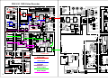
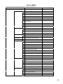
Overall Block Diagram
FAN (DRV2)
234
# " %
356
# "
%'
)*
%
)*
%'
"#
%'
"#
"#
"#
"
"#
("
!"
;
- .
""-
""-
""-
#%%$
)%*
)%*
('$
(+
(+
#
,'
"#
"
" $ *
*
1/2 PCIB ASSY
"
FLASH
32M
$
*
$0 *
*
,'
,'
# ,
,
-
-
,
)*
)*
-"#
,"#
,
-
)*
"#
"#
,'
,'
,
,
-
-
&
$
&
%
KEYB
ASSY
&
01
!
$
1/2
PWRB
2
,6
ASSY ,6
,6
1 ,6
664
664
1614
# #
#
8589:
2/2 ATX
POWER
120GB HDD
$6
161
%
2
23
2 2 2
MASTER
DRIVE 1
1
&$
,
%
REAR USB (4Px2)
,
7
2
2
23
4
1 %
1 ,
,
2
1
USBB ASSY
,
2 1 ,
1/2
ATX POWER
2 664
VGA
1 UPS
7
,&
664
ETHERNET (15P)
FLKB
ASSY
2
2
1614
23
SLAVE
DRIVE 2 (OPTION)
2
2
2
%
,
/
,/,
1
%
2
2
PC Mother Board
%-%
0%
( $
%
,
86
8
8
$
2
" 2
2 IDE 2
'
)*
'
" 2 %
2
)*
)*
2 #
(
,
2
" "#
'
'$
2 $
2
# "
%%
/
&
2
AVIB ASSY
,
RS422
Control
2+
2+
2+
?$
$
8
2
?
# "
2+
*
*
23
*''-.
$ , &
?
2+
%'
(2'
'
%
"#
'
?$
?
# "
?
%
(2'
2+
)*
)*
,'
)*
23
/
@%(>
%'
(2'
(2'
(> %
%!
%#
$2
"
%'
(2'
%
01
!
"
?
'
&'$#
%/
&'$#
""-
%
)*
)'*
"( :)
!"#
# #
%
)*
01
,
1/3
* +
$2
#
(
#
%''
$
"#
2"
""-
89=
""-
'((!) #
.;
!
("
"
(> "
"
%
'
/
&'$#
%
"#
(
("
"#
$% $&
&% (
)*
)*
%'
"#
:<5
!"
DRV2B
ASSY
2 ,6
,6
!"
"#
86
" 2 "
" - !"
8=85
)'*
"
'
)"2*
) *
%-
%
%-
%
&'$#
%'
"#
"#
"
7858
&'$#
# "
!$
! ')"2*
DECB ASSY
,6
'
' '
8589:
! !"
+& $
8
/
DVI OUTPUT
COM 2
'
'-'0
')"2*
%
$
"
,
"
"
'
# "
* 1
/,
"
DRV1B
ASSY
2/2 PWRB ASSY
PCI SLOT 3
IDE 1
FAN (REAR
,6
MASTER
FAN (DRV1)
2/3
)*
,'
$
)*
'')*
PCI SLOT 2
'')*
-
'')*
-%
" " $
)*
"
" ""
-
!$
'
)*
)*
6
6
26
26
5
FRONT USB
(4Px2)
4.
Block Diagram Overview
(JKIB Assembly)
All inputs Video and Audio (Composite, Component Beta or SMPTE,
S-Video, DV, Balanced and Unbalanced Audio) enter and pass
though the JKIB assembly and enter the AVIB assembly. If using the
composite input in through mode the unprocessed audio and video
pass back directly to the JKOB output assembly for monitor viewing.
(AVIB)
Video and Audio signals entering the AVIB assembly are subject to
analog to digital conversion, time based correction and digital noise
reduction will be added if selected by the user. On this assembly the
signals next are MPEG encoded and sent out to the PCIB assembly.
(PCIB)
The two main functions of the PCIB assembly are.
1. RS422 control interface.
2. PCI interface for the MPEG encoded signals.
Output signals from this board enter the PC Mother board (PCI slot 3)
(DECB)
The DECB assembly receives its input from the PC Mother board
(PCI slot 2) into its PCI interface conversion IC. After conversion back
to a MPEG stream the signals pass through the MPEG decoder and
digital to analog converters for both audio and video. At this point the
analog video and audio output to the JKIB assembly.
(JKOB)
The JKOB or jack panel output board receives input audio and video
signals from the JKIB assembly. In turn it outputs directly to the back
panel.
5.
Block Diagram Overview
(PC Mother Board)
The main circuit board assembly in this device is a very high quality
Pentium based personal computer main board. It interfaces directly
with the front panel control by an RS232 connection on COM 2. In
addition it has front and rear USB ports, a RS232 connection for a
UPS, 3 PCI slots (2 used), an Ethernet connection and VGA output.
Main system processor (Intel Celeron 2 GHz) with 256 Mb ram.
(ATX Power)
The ATX power assembly is similar to a home or office PC supply. It
provides +12, -12, +5, -5 and +3.3 voltage supplies to the PWRB
assembly.
(PWRB)
This main power supply assembly provides DC supply to all circuit
boards and drives 3 of the 5 fans used in this product.
(JKDB)
This assembly contains the RS422 interface and output RS422
connector. It also interfaces the external sync input to the DECB
board and the LTC (linear time code) to the PCIB board.
(422IB)
The RS422 input connector assembly provides input to the 422 driver
IC located on the JKDB board.
(HPVB)
Headphone output volume and driver assembly. Located on the front
panel.
(FLKB)
Front panel assembly. This board includes the florescent display
driver and IR remote control decoder. This board along with its main
CPU communicate directly to the PC motherboard through the RS232
Com 2 port.
6.
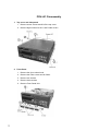
PRV-LX1 Disassembly
1. Top cover and side panels
1. Remove seven screws and lift off the top cover.
2. Remove eight screws for the L and R side covers.
2. Front Panel
1. Remove the front volume knob.
2. Remove the Filter covers and Air filters.
3. Remove two screws.
4. Remove three screws
5. Remove Front Panel Unit.
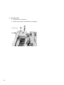
7.
Front & Rear Bridges must be removed in order to access drives and board
assemblies.
1. Remove 12 screws for the front & 8 screws for the rear bridge.
2. Remove bridges.
8.
3. Drive Assy LX1
1. Disconnect two connectors.
2. Remove four screws and DVDR Drive Assembly.
9
9.
4. HDD Assy
1. Disconnect two connectors.
2. Remove four screws.
Attention: One screw is under the label.
3. Pull up on the handle and remove HDD Assy.
10.
5. AVIB Assy
1. Remove four screws.
2. Remove Rear bridge.
3. Disconnect four FFC cables and four connectors.
4. Remove four screws.
5. Remove AVIB Assy with AVI shield and base.
11.
6. JKIB Assy & JKOB Assy
1. Disconnect two FFC cables and a connector.
2. Remove nine screws (JKIB Assy).
3. Remove nine screws (JKOB Assy).
4. Remove three screws.
5. Remove JKIB Assy with PCI cover and Jack stay.
X
6. Remove JKOB Assy.
12.
7. DECB Assy & PCIB Assy
1. Disconnect two connectors.
2. Remove two screws of Rear Panel.
3. Remove two screws.
4. Pull up DECB Assy from PCI slot of Mother Board.
5. Pull up PCIB Assy from PCI slot.
6. Remove two screws, 4P Power connector and Flat cable clamp.
13.
8. PWRB Assy
1. Remove Center stay and Front Bridge with 12 screws.
2. Disconnect eight connectors.
3. Remove three screws.
4. Remove the hook of Card edge spacer.
5. Remove PWRB Assy.
14.
9. MOTHER BOARD Assy
1. Disconnect two connectors.
2. Remove seven screws.
3. Remove MOTHER BOARD Assy
10. ATX Power Supply Unit
1. Remove one screw inside.
2. Remove four screws outside.
3. Remove ATX Power Supply Unit.
15.
11. Exchange the FAN of Power Supply
1. Remove a screw and move switch barrier.
1. screw
Switch barrier
2. Remove Fan cover and disconnect a connector.
Fan connector
3. Exchange the FAN.
4. Connect FAN connector.
5. Install Fan cover.
6. Move switch barrier and secure a screw.
16.
*Cable Styling of Power Supply
17.
Service Mode
Test mode Function List Using Service Remote Control (GGF1067 or GGF1381)
Input Remote Control Code
Function
[ESC]+[TEST]
Test Mode
[CX]
memo
FAN Test Mode
[0]
All FAN ON
[1]
All FAN OFF
[2]
Left FAN ON
[3]
Left FAN OFF
[4]
Right FAN ON
[5]
Right FAN OFF
[6]
Rear FAN ON
[7]
Rear FAN OFF
[9]
Exit
[P.RUN]
LED/FL Test Mode
[0]
Exit
[1]
Turn on all FL/LED light
[2]
Turn off all FL/LED light
[TV/LDP]
Front Panel switch Test Mode
[0]
Exit
[STEREO]+[8]
Region number of Drive1 on display
[STEREO]+[9]
Region number of Drive2 on display
[REP.A]
System Information on display
[0]
Exit
[1]
Main System on display
[2]
USB Interface on display
[3]
Network Interface on display
[4]
Primary Master Drive on display
[5]
Primary Slave Drive on display
[6]
Secondary Master Drive on display
[7]
Secondary Slave Drive on display
[8]
Error History of Drive1 on display
[9]
Error History of Drive2 on display
[REP.B]
*1
*2
connected Drive2
connected Drive2
Loop back Test Mode
[0]
Exit
[1]
RS-422A Loop Back Test
[2]
RS-232C Loop Back Test
[3]
RS-422A Loop Back Test (Error Stop)
[4]
RS-232C Loop Back Test (Error Stop)
[A.MON]
Power On Time Clear
[0]
HDD Access Time
Caution! This will clear the timer
[1]
Power On Time of PRV-LX1
Caution! This will clear the timer
[8]
Copy the setting file
for using FTP(Network)
[9]
Copy the log file
for using FTP(Network)
18.
Service Mode
Input Remote Control Code
Function
[ESC]+[TEST]
Test Mode
[PLAY]
memo
Measuring Error Rate
[ESC]+[TEST]
[SCAN F]
+0x10000
[SCAN R]
-0x10000
[1]
Start measuring of Drive1
[2]
Start measuring of Drive2
▲/■
Stop measuring
[0]
RS-422A and 232C Interface Test
[1]
RS-422A Loop Back Test
[2]
RS-232C Loop Back Test
[3]
LAN Test
[4]
USB Test
[5]
Measuring Error Rate of Drive1
[6]
Measuring Error Rate of Drive2
[7]
LTC on FL
[CLEAR]
Clear on display
[ESC]
Escape Test Mode
Auto start [1]-[4]
*3
(ESC)+(front panel buttons or remote control Open or close drive trays
[ESC]+[DISP]
Debug Mode
[DISP]
*4
Enter next page
---Page1--- : PRV-LX1 Information
---Page2--- : DVD Play Information
---Page3--- : Decode Information of DECB Assy
---Page4--- : Encode Information of PCIB Assy and AVIB Assy
---Page5--- : Encode Information of Application
---Page6--- : Linux information
*1: Test mode of front panel button input
When you enter this mode all segments on the FL display light up. Pressing front panel keys will turn off segments
one by one.
After the all keys have been pushed, only 3 blocks remain on. (only 2 blocks-> with 2 drives)
*2: System Information on display
[1]: Main System
-CPU
--- Confirmation of the CPU clock
-Memory
--- Confirmation of the capacity of memories
-User Data
--- Confirmation of the free space of the HDD (User Area)
-PCI
--- Confirmation of the PCI boards was recognized from Linux OS
[2]: USB
- Connected USB products on display. (keyboard & mouse)
[3]: Network
-IP Address/Network/MAC Address
19.
Service Mode
-10base/100base
[4]: HDD (IDE Primary-Master)
-Information of connected HDD
[5]: HDD (IDE Primary -Slave)
-No connect
[6]: DVD-R/RW (Drive1)
-Information of Drive1
[7]: DVD-R/RW (Drive2)
-Information of Drive2
[8]: Error History of Drive1
[9]: Error History of Drive2
*3: Measuring the error rate of DVD drive unit
[5]: Drive1
-Insert the disc and select this function.
-Threshold level (3.3e-3) DVD-ROM,-R-RW
[6]: Drive2
-Insert the disc and select this function.
-Threshold level (3.3e-3) DVD-ROM,-R-RW
*4: Debug mode
-[ESC]+[DISP]
: Enter the debug mode.
-[DISPLAY] : Select the next page.
-[SIDE-A or B]
: Enter the sub mode of debug mode.
-[ESC]
: Escape the debug mode.
---Page 1---: PRV-LX1 information
-Program
: application version
-OS
-FLCOM
: os version
: FL cpu version
-VD-RW
: Firmware version
-Shimuke
: 0: Japan model, 1: KU model (USA), 2: WY model (EU)
: (1/1/-1)
: Region number (Decoder board/Drive1/Drive2)
: -1 means no connection
---Page 2---: Engineering use only.
--Page 3---: Decode Information of DECB Assy
20.
Service Mode
-Select the error history --> Push [SIDE-A] on GGF1067 one time.
“No device error” on display stands for no error.
“The numbers on display stands for error code.
(Ex.)
10-030305210700
40-030306093005
50-030401112233
04-030405131500
EE-YYMMDDHHMMSS
EE: Error code, YY…..SS: Date
50(error) stands for 40(error) and 10(Error) ware occurred at the same time.
Error Code
Detail
01
Xiline Configurations Error
04
SH SDRAM Access error
10
Video Encoder Initialize Error
20
AV Decoder Initialize Error
40
AV Decoder SDRAM Access Error
Note: Press Side-A
again for more error
information. Pages 3,
4 and 5.
---Page 4---: Encode Information of PCIB and AVIB Assy
-Select the error history --> Push (Side-A) to Enter the sub mode.
2003/07/29 10:30:20 == 09 03 ==
(
Data
)
(EC)
Error Code
Detail
Error Code
Detail
01
Data Read Time error
D3
Reset Error (AUDIO Enc.)
02
Copy Protection Error
D4
Initialize Error (AUDIO Enc.)
03
task 09: Illegal frame number Error
D5
Standby Error (AUDIO Enc.)
03
task 32: No digital signal Error
D6
Command Error (AUDIO Enc.)
04
PCI Destination Address Timeout Error
D7
Command Timeout Error (AUDIO Enc.)
05
PCI Map Timeout Error
DC
Hard Error (VIDEO Enc.)
C9
Hard Error
DD
Reset Error (VIDEO Enc.)
CA
Reset Error
DE
Initialize Error (VIDEO Enc.)
CA
task 0A: Stream Buffer Full Error
DF
Standby Error (VIDEO Enc.)
CB
Initialize Error
E0
Command Error (VIDEO Enc.)
CC
Standby Error
E1
DV Decode Error
CD
Command Error
E2
DV Encode Error
CE
Stream Timeout Error
E3
FS Change Error (before)
CF
Command Timeout Error
E4
FS Change Error (After)
D0
Buffer Full Error
E5
Command timeout Error (VIDEO Enc.)
D2
Hard Error (AUDIO Enc.)
E6
Command Execute Error (VIDEO Enc.)
Notes: No page 5 unless in record mode. Page 5 functions the same as page 4.
Page 6 for Engineering use only.
21.
Viewing and Confirmation of log files
<Items Needed>
1. Personal Computer with LAN card
2. Network cable (Cross type)
<Method of opening a log file>
1. Setup Network connection of the personal computer.
IP Address: 192.168.0.15
Subnet mask: 255.255.255.0
Gateway: 192.168.0.1
2. Turn off the personal computer.
3. Set Network connection of the PRV-LX1.
IP Address: 192.168.0.16
Subnet mask: 255.255.255.0
Gateway: 192.168.0.1
4. Turn off PRV-LX1.
5. Connect the personal computer to PRV-LX1 with Network cable.
6. Turn on PRV-LX1 and the personal computer.
7. Open the log files using IE (Internet Explorer).
8. Input “ftp://192.168.0.16” at IE.
9. Input the user and password.
User: DVDRecService
Password: DVDRecService
10. Open “poweron.log” using Internet Explorer (save file and open with Excel)
22.
<Log list>
POWER-ON=7 ------- Power on Times
1 : Power On : Mon Jun 23 21:19:26 EDT 2003 ------- Power on date
Shimuke=x, Region=x,x,x PowerOnKey=xxxxx
Power Off : Mon Jun 23 22:12:16 EDT 2003 ------- Power off date
2 : Power On : Tue Jul 8 10:10:12 EDT 2003
Shimuke=x, Region=x,x,x PowerOnKey=xxxxx
3 : Power On : Tue Jul 8 10:12:32 EDT 2003
Shimuke=x, Region=x,x,x PowerOnKey=xxxxx
----- Found a power failure in the previous power on ----- ----Found a power failure
Power Off : Tue Jul 8 10:15:16 EDT 2003
4 : Power On : Tue Jul 8 14:10:22 EDT 2003
Shimuke=x, Region=x,x,x PowerOnKey=xxxxx
!!!!!! The root file system has been recovered !!!!!!!! ---The files have been recovered
Power Off : Tue Jul 8 14:12:16 EDT 2003
5 : Power On : Tue Jul 8 15:10:22 EDT 2003
Shimuke=x, Region=x,x,x PowerOnKey=xxxxx
!!!!!! NO DECODER BOARD ERROR (REBOOT) !!!!!!!!
--Not detect decoder unit
6 : Power On : Tue Jul 8 16:10:22 EDT 2003
Shimuke=x, Region=x,x,x PowerOnKey=xxxxx
!!!!!! NO DECODER BOARD ERROR AGAIN !!!!!!!! --Not detect decoder unit
Power Off : Tue Jul 8 16:12:16 EDT 2003
7 : Power On : Tue Jul 8 18:10:22 EDT 2003
Shimuke=x, Region=x,x,x PowerOnKey=xxxxx
23.
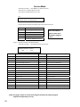
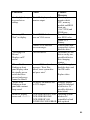
PRV-LX1
Ass'y Ass'y No. ST LED
PWRB DWZ1106 D9
HDD_IND
D10
V+5VSB
D11
V+5V
D12
V+3.3VD
D13
V+2.5VD
D19
V+5VSB_M
D24
FAN DET
D25
PS_ON
Status LED's
Function
HDD access indicator
Check STB +5V line
Check +5V line
Check +3.3V line
Check +2.5V line
Check STB+5V line for MB
Check FAN status
Status of LED on
HDD access
Output +5V from Power supply (STB+5V line)
Output +5V from Power supply (+5V line)
Output +3.3V from IC201
Output +2.5V from IC101
Output +5V from RY1 (+5VSB line)
STB or FAN status is okay
Without Option Drive: Check REAR and Drive1 FAN all time
With Option Drive: Check REAR, Drive1 and Drive2 FAN all time
Check PS_ON signal from
MB
Output high level signal from STB or MB
When D25 is on, D11, D12 and D13 are off.
PS-ON sequence
1. Turn on the rear power switch -> Light on D10, D24 and D25
2. Turn on the front power switch -> D19 light on,
and then D25 light off, next D11, D12 and D13 light on.
finally D681(USBB) light on.
PCIB DWP1080 D2101 V-12V
Check PCI -12V line
Output -12V from MB
D2102 V+12V
Check PCI +12V line
Output +12V from MB
D2301 V+5M
Check PCI +5V
Output +5V from MB, TH2351(PolySwitch) is okay
D2304 FPGA active Check the status of Xilinx IC Default: light on, trance far data: blink
D2305 PTD[0]
Status: the encoder [0]
Error status (power on)
Status: the encoder [1]
D2306 PTD[1]
LED status
[3][2][1][0]
Status: the encoder [2]
D2307 PTD[2]
No error
0000
Status: the encoder [3]
D2308 PTD[3]
PCIB Xilinx ( IC2309 )
0001
AVIB Xilinx ( IC5004 )
0010
reserved
0011
SDRAM ( IC2404 )
0100
Slalom ( IC2001 )
0101
Slalom SDRAM ( IC2003 )
0110
George ( IC3502 )
0111
Vaikilt ( IC5002 )
1000
Aprilia ( IC6003 )
1001
Celynx ( IC4001 )
1010
Dvxcel ( IC7004 )
1011
Audery ( IC6002 )
1100
DECB
D1181 PTD[0]
Status: the decoder [0]
Normal:
D1182 PTD[1]
Status: the decoder [1]
Play
random
D1185 PTD[2]
Status: the decoder [2]
Stop
All LED turn off
D1186 PTD[3]
Status: the decoder [3]
Error Status:
Flash writing NG
All LED turn on
Xilinx Configuration Error all LED blink 1sec by 1sec
SH SDRAM Error
D1181 turns on
Video Encoder Initialize ErrD1182 turns on
AV1 Initialize Error
D1185 turns on
AV1 SDRAM Error
D1186 turns on
AVIB DWV1198 D3201 V+12I
Check +12V line
Output +12V from PWRB
D3202 V+5DI
Check +5V line
Output +5V from PWRB, IC3205 (ICP-S2.3) is okay
D3203 V+3_3I
Check +3.3V line
Output +3.3V from PWRB
D3204 V+2_5I
Check +2.5V line
Output +2.5V from PWRB
D5001 ENC OK
Check the status of Xilinx IC Default: light on, transfer data: blink
D5002 WMKD7
Status the encoder [3]
=PCIB Error Status:
Status the encoder [2]
D5003 WMKD6
Status the encoder [1]
D5004 WMKD5
Status the encoder [0]
D5005 WMKD4
24.
PRV-LX1 Trouble Shooting
Items needed:
USB Keyboard
VGA Monitor
USB Mouse
Volt Meter
Network Crossover Cable
Service Manual
Test Discs (DVDR, DVDRW)
Service Remote GGF1381 or GGF1067
Overview: The PRV-LX1 is a Computer based product
with wireless remote control capability and a front
panel interface. Basic overall troubleshooting of this
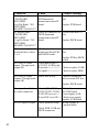
device will be similar to that of a Personal Computer.
Condition
Check
Counter
Measure
No standby light with
the main power
switch on (back
panel).
Check condition of
LED (D10) located on the
(PWRB) board.
If LED is off check
ICP (IC8) and
supply from ATX
power board.
Possible defective
ATX or PWRB
board.
Check connector
CN3 (PWRB) to
(FLKB). Possible
defective PWRB
Board.
Check (D10) on
(RED).
25.
Condition
Check
Counter
Measure
Standby light changes
to green but no
startup.
Check FL display and
monitor output.
No startup “Please
Wait” on display.
Check CMOS checksum
error on VGA screen.
If no display or
monitor check
CPU, memory
module and BIOS
short pin.
(1 & 2 JP14) and
FLKB assy.
Press F1 to load a
new BIOS value.
Check 2.5V
Battery.
If error reads (nonsystem disc) replace
hard disc drive.
Disconnect DVDR
drives one by one,
possible defective
drive hanging
startup.
Check DC supply to
hard disc drive and
flat IDE cable.
Connect VGA and read
screen messages.
“Detecting IDE
Drivers”
Displays on PC
screen.
Check all drives.
“Please Wait”
flashing on front
panel display when
the standby power
switch has been
pressed and power
cannot be shutoff.
“Please Wait”
flashing on front
panel and constant
beep sound.
Connect VGA and read
messages. “Boot Disc
failure, insert system disc
and press enter”.
On the FL display
errors read >>>>>>>
Replace drive.
No display on monitor and
no VGA output.
Memory module
could be dislodged
of defective. Or
possibly defective
main board.
FSCK-ERROR BOOT/USR Operating system
FSCK-ERROR HOME
needs to be
FSCK-ERROR VAR
reinstalled or hard
POWER ON FSCK-ERROR disk replaced
26.
Condition
Check
Counter Measure
FL display reads:
“NO BOARD
ENCODER”
Log File Reads: “NO
ENCODER
BOARD!!!!AGAIN!!!!”
FL display reads:
“NO BOARD
DECODER”
Log File Reads: “NO
DECODER
BOARD!!!!AGAIN!!!!”
No record or playback
from hard disc or drive
1 or 2.
Check all connectors on Reseat board into PCI
PCIB board and
slot.
connection to main PC
board.
Replace PCIB board.
Check all connectors on Reseat board into PCI
DECB board and
slot.
connection to main PC
board.
Replace DECB board.
Check connection to
main board from PCIB
and DECB boards.
Reseat boards into PCI
slot.
Replace PCIB or DECB
boards.
No Video or Audio
inputs. Through mode
output OK.
Video input at pin 10
(CN3501) AVIB board.
If present>>>>>>>>>>
No signal>>>>>>>>>>
No Video or Audio
outputs. Through mode
output OK.
Check DECB assy.
Check or replace AVIB.
Check or replace JKIB.
Check all connectors
and reseat into PCI slot.
Replace DECB board.
No output from Video
or Audio connectors.
Check LED’s D3201,
D3202, D3203, D3204.
If all LED’s are on>>>
If any LED’s are Off>>
No DV input or output.
Check operation setup.
Check JKIB, AVIB and
DECB connectors.
27.
Check all connectors to
the AVIB board.
Power Supply is OK.
Check power supply.
Replace AVIB board.
Wrong settings in
Function Menu.
Condition
Check
Counter Measure
No RS422 control.>>>> Check operation setup. Correct settings in
Check JKDB and PCIB Function Menu.
connectors.
No RS232 control.
Run Loop Back Test in
No LAN control.
service mode.
Not locking on External Check operation setup
Sync input.
(rear panel switch).
Correct switch setting.
Check JKDB and
DECB connectors.
Notes:
Utilizing Service Mode in conjunction with the monitor
output, front panel display and VGA output will
considerably shorten troubleshooting time.
(See Service mode & Log File sections)
Most all PC board assemblies in this device have LED
Status indicators that can be used to detect problems.
(See LED Status section)
28.
6dB
AMP
JKIB ASSY
SYNC
SEP.
JA7941
Ex Sync
Y
LTC
JA7402
CV
CLAMP
CN7611
AMP
AMP(Beta)
Y
AMP(SMPTE)
Cb
CN7901
Thru
JA7403
422
DRV/RCV
CN7903
AMP(Beta)
Cr
CN7952
AMP
AMP(SMPTE)
AMP
AMP(SMPTE)
JA7601
Thru
L
R
CN7951
AMP(Beta)
2
V Select
Thru
A Select
Beta/SMPTE
422 IB ASSY
CN3501
Thru
JA7961
XLR
L
AMP
XLR
R
AMP
CN7402
JA7404
DV
CN4001
JA7854
LTR/SQZ
Y/Cb/Cr
Y/Cb/Cr
IC7803
P/I
Cr
Y/Cb/Cr
JA7852
CN7801
Y
Cb
Y/C
JA7853
CV
CV
JA7855
SPDIF
JA7851
6dB
CV
Thru
CN7802
Y/C
CN7851
Y/C
CN1811
SPDIF
Thru
L
L
R
AMP
AMP
XLR L
MUTE
Thru
JA7981
R
XLR R
AMP
JKOB
ASSY
HPVB
ASSY
+5V
+9V
+9V
-9V
MUTE
CN7613
CN7701
6dB
AMP
CN661
JA661
29.
COMP
AMP
CN3202
CN1471
JKDB ASSY
S7941
CN7941
C
CN7902
JA7401
IC1311
PCI I/F
Xilinx FPGA
IC1211
MPU
SH-3
SH-3_ADRS
PCI BUS
SH-3_DATA
SH-3_CTRL
MPEG_
BITSTREAM
IC1512
64M
SDRAM
IC1513
MPEG Dec.
AV-1
IC1612
32M
FLASH
IC1611
64M
SDRAM
P/XI
Y/Pb/Pr
IC1851-IC1853
ANALOG
SW
Component
Y/Cb/Cr
AV-1_VIDEO
IC1711
VIDEO
Enc.
Composite
S-VIDEO (Y/C)
AV-1_AUDIO
IC1751
AUDIO
DAC
Audio (L/R)
: Digital Signal and Control Signal
: Digital AV Signal
: Analog Video Signal
: Analog Audio Signal
30.
B
JKDB ASSY
AVIB ASSY
DECB ASSY
CN7902 (11 pin)
CN1183 (7 pin)
CN3301 (4 pin), CN3002 (50 pin), CN3001 (50 pin)
CN2102 (11 pin)
CN2405 (7 pin)
CN2101 (4 pin), CN2103 (50 pin), CN2104 (50 pin)
RS232C
MPEG
Stream
MPU BUS
RS422
IC2405
HD6417709AF100B
MPU
IC2406
MBM29DL322BE90PFTN
IC2309
XC2S100PQ208
32M FLASH ROM
Pcif Xilinx
PCI BUS
IC2404
K4S643232F-TC60
64M SDRAM
(Main Memory)
IC2001
PD5219
Slalom
(DMA Control,
CPU IF, etc.)
IC2003
HY57V641620HGT-7
64M SDRAM
(Stream Buffer)
PCIB ASSY
CN2301, CN2302 (PCI Card Edge: 124 pin)
MOTHER BOARD ASSY
31.
From DINB ASSY
(OPTION)
CN8203
Digital Video Signal
From DOOB ASSY
(OPTION)
CN8602
CN5501
DV I/O Signal
CN5503
SDI_D0,7
Video656
data
DECB ASSY
CN1651
CN6002
AVI_D0,7
Video656
data
SDO_D0,7
Video656
data
AVIB ASSY
CN3501
Analog Video V or Y
Analog Video C
R_ADD0,7
IC3501
George
Video A/D
Analog Video Cb
Analog Video Cr
IC5004
LTC_SW
XILINX
Video656
data
F_AD0,7
IC5001
64M SDRAM
IC5002
Vaikilt
TBC/DNR
Video656 data
L_A1,9
L_D0,15
CN7611
L_A0,7
L_A0,7
L_D0,7
JKIB ASSY
L_D0,7
D_DVDR0,7
Video656
data
D_DVD0,7
Video656
data
Host Address/Data Bus
1394
Differential
CN4001
IC4002
DVPhysical
PHY0,7
DVI0,7
DV Stream
data
IC4001
DV Stream DV-Link
data
L_A1,3
CN7402
A
JKIB ASSY
L_D0,15
L_A1,9
IC7002
64M SDRAM
IC7004
DVXcel
MPEGENC
DV CODEC
IC7003
64M SDRAM
L_D0,15
Host Address/Data Bus
EBSDW0,7
MPEG data
L_A0,15
L_D0,15
IC3004
BUF
IC3002,IC3003
BUF
IC3002,IC3003
BUF
EBS0,7
MPEG data
C_A0,15
C_D0,15
CN3002
CN3001
CN2103
CN2104
PCIB ASSY
PCIB ASSY
To SDIB
From SDIB
27MHz which was locked with SDI signal
From Vaikilt
PCO
PLL Control Signal
VCXO
27MHz
Oscillation
Block
A
B
IC3308
27MHz
BUF
27MHz
To each device
Multiplexer AHC2G53
IC3309
PLL1700
PLL IC
IC3310
BUF
18.432MHz
To each device
36.864MHz
To each device
32.
From DINB ASSY
(OPTION)
CN8203
Digital Audio Signal
From DOOB ASSY
(OPTION)
CN8602
CN1651
CN5503
CN6002
H
CN5501
CN3501
DV I/O Signal
SDI_DAI,SDI_BCK,
SDI_LRCK,AESI_DAI,
AE S I_BCK,AESI_LRCKI
Analog Audio
RCA or XLR
IC3801
TC9412A
EVolume
IC3802
PCM1800
Audio A/D
ADATI,
BCKI,
LRCKI
DECB ASSY
AV1_DAI,AV1_BCK,
AV1_LRCK
SDO_DAI,
SDO_BCK,
SDO_LRCK
IC5004
LTC_SW
XILINX
AVIB ASSY
Recording only
FADATI,FBCKI,
FLRCKI
L_A0,15
ADATAO,BCKAO,
LRCKAO
IC6003
Aplilia
Audio I/F
ADATSR,BCKSR,
LRCKSR
L_AD0,7
IC6002
Audery
AC3ENC
CN7611
A
ADATDX,BCKAU,
LRCKAU
L_D0,15
JKIB ASSY
L_A0,7
L_D0,7
ADATDV,
BCKDV,
LRCKDV
Host Address/Data Bus
1394
Differential
CN4001
IC4002
DVPhysical
PHY0,7
IC4001
DV Stream DV-Link
data
DVI0,7
DV Stream
data
L_A1,3
CN7402
JKIB ASSY
L_D0,15
L_A1,9
ADATSO,BCKSOI,
LRCKSO
ADATSI,BCKSI,
LRCKSI
ADATX,BCKAPX,
LRCKX
IC7004
DVXcel
MPEGENC
DV CODEC
L_D0,15
Host Address/Data Bus
L_A0,15
L_D0,15
IC3004
BUF
IC3002,IC3003
BUF
C_D0,15
CN3001
CN2104
G
33.
EBSDW0,7
MPEG data
PCIB ASSY
C_A0,15
EBS0,7
MPEG data
CN3002
CN2103
PCIB ASSY
IC6004
CS8420
SRC
IC7002
64M SDRAM
IC7003
64M SDRAM
+D1, -D1, +D2, -D2
CN1
+3.3,±5,±12V
+5VSB,PWR_OK
PS_ON
PWR_SW
+5VSB
PWRB ASSY
PWR_OK
CN2
AVIB Block
CN681
+5V
CN5
CN684
N
USBB ASSY
USB+5V
+3.3,±5,±12V,
PWR_OK
CN4
MOTHER
BOARD
ASSY
ATX
PSU
FANCONT(Rear)
CN9
FANCONT(DRV1)
CN10
FANCONT(DRV2)
9
CN3
CN11
CN501
Serial
Communication
Block
CN504
COM2
3
V+5V_FLK
LED
Block
SIN
IC501
FL UCOM
2 SOUT
SW
Block
1
Digital Input
Analog Input
J
FLKB ASSY
IC502
FL DRIVER
IC503
FL DRIVER
V501
FL TUBE
V502
FL TUBE
CN503
CN502
CN601
CN631
KEYB ASSY
SW
Block
Digital Input
LED
Block
SW
Block
Digital Input
Analog Input
Analog Input
LED
Block
CN602
CN641
DRV2B ASSY
SW
Block
Digital Input
LED
Block
DRV1B ASSY
Analog Input
34.
I
PWR_OK
PWRB ASSY
Power Control Block
USBB ASSY
+2.5V Power
Generation Block
AVIB ASSY
+3.3V Power
Generation Block
AVIB ASSY
+12V Power
Generation Block
FAN
+5V
To
ATX
POWER
SUPPLY
UNIT
CN1
-31V FL Power
Generation Block (-30.5V)
FLKB ASSY
-28V FL Power
Generation Block (-27.0V)
FLKB ASSY
-24V FL Power
Generation Block (-23.5V)
+5VSB
+5VB
FLKB ASSY
FLKB ASSY, PWRB ASSY
Power Control Block
CN4
To MOTHER BOARD ASSY
PWR_SW
+3.3V
+5V
+12V
-12V
-5V
35.
CN4
To MOTHER BOARD ASSY
FAN_CONT(DRV1)
FAN
FAN_CONT(DRV2)
FAN
FAN_CONT(Rear)
FAN
FAN Detection Block
FLKB ASSY
How to install upgrades or the Program
Operating System
1. With the unit in the “Standby condition” press
Enter and Standby for at least 3 seconds. Wait for
the unit to power up and tray one will open
automatically. Florescent display will read
“Program-Install”.
2. Insert the Program Disc and press Enter for 2
seconds. Florescent display will read “DownloadFull”.
3. Using the composite video output monitor the
program downloading progress.
4. When the program has finished downloading both
DVDR trays will open automatically and the unit will
power down back to standby condition. (Leaving
the trays open).
5. Power the unit back up and check for revision
update numbers by entering the Function
menu/Setup/System/Information.
Note: Total upgrade time will be about 5 minuets
36.