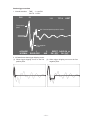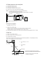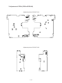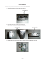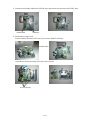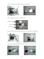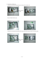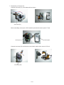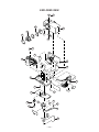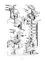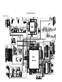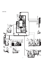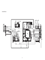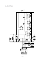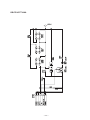
1
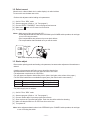
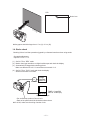
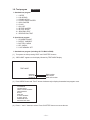
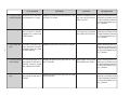
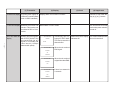
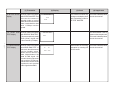
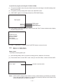
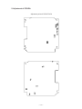
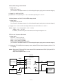
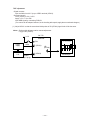
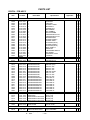
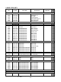
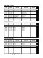
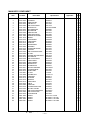
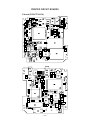
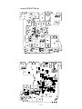
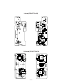
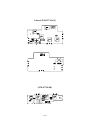
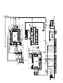
(without price)
QV-770
(KX-773)
APR. 1998
INDEX
R
CONTENTS
SPECIFICATIONS ......................................................................................................................................1
BLOCK DIAGRAM .....................................................................................................................................2
ADJUSTMENT ...........................................................................................................................................3
1-1. Loading color parameter ................................................................................................................3
1-2. Defect correct ..................................................................................................................................4
1-3. Strobe adjust ...................................................................................................................................4
1-4. Strobe check ...................................................................................................................................5
1-5. Display appearance when using flash. ......................................................................................... 7
1-6. Current consumption .....................................................................................................................7
1-7. IrDA Test ..........................................................................................................................................7
1-8. Test program ...................................................................................................................................8
1. Standard test program (including QV-770 Built in ROM) ........................................................8
2. Special test program (including QV-770 Built in ROM) ......................................................... 12
Battery check ............................................................................................................................12
Key check ..................................................................................................................................13
Last memory set .......................................................................................................................13
2. Adjustment of PCB-DA .................................................................................................................... 14
Adjustment of VCC7, VCC3, voltage check of VCC1 ....................................................................15
Operation Check ..............................................................................................................................15
3. Adjustment of PCB-L .......................................................................................................................16
VCC3, VCC5 voltage check LA-PCB ..............................................................................................17
VCC2 adjustment and VCC7, VCC8, VEE2 voltage check ...........................................................17
VCO free run frequency adjustment ..............................................................................................17
BL drive voltage adjustment ........................................................................................................... 18
VCOM AC adjustment and VCOM DC coarse adjustment ............................................................18
Bright voltage setting and contrast adjustment (PCB-LA) ..........................................................19
Color adjustment (PCB-LA) ............................................................................................................19
TINT adjustment ...............................................................................................................................20
DISASSEMBLY ........................................................................................................................................21
EXPLODED VIEW .................................................................................................................................... 26
PARTS LIST ............................................................................................................................................. 28
PRINTED CIRCUIT BOARDS .................................................................................................................. 33
SCHEMATIC DIAGRAMS ........................................................................................................................37
TROUBLE SHOOTING ............................................................................................................................43
SPECIFICATIONS
Item
Recording System
Specification
Digital (JPEG base); PC Link software can be used to input images in CAM,
JPEG, TIFF and other format.
Signal System
NTSC
Recording Medium
Flash memory (4 MB)
Memory Capacity
FINE; 30 images (Approx. 124 KB compressed)
NORMAL; 60 images (Approx. 62 KB compressed)
ECONOMY; 120 images (Approx. 32 KB compressed)
Imaging Element
1/4-inch CCD (Total Pixels: 350,000; Effective Pixels: 330,000)
Lens
Fixed focal point with macro position; F2, f = 3.9 mm
Focus Range
NORMAL: 70 cm to ∞
MACRO: 14 cm to 16 cm (From surface of protective lens)
Light Metering
TTL center priority by CCD
Exposure Metering
Program AE, Aperture Priority AE
Exposure Range
EV +5 to 18
Exposure Correction
–2 EV to +2 EV (1/4 EV units)
Shutter
CCD shutter
Shutter Speed
1/8 to 1/4000 second
White Balance
Automatic, Fixed
Self-timer
10 seconds
Flash Modes
Auto Flash, Flash On, Flash Off
Resolution Modes
FINE, NORMAL, ECONOMY
Monitor/Viewfinder
1.8” TFT, low-glare color LCD (122,100 pixels)
Computer output image
640 × 480 pixels
Input/Output Terminals
DIGITAL OUT, VIDEO OUT, AC adaptor connector
Clock
January 1, 1997 00:00:00 to December 31, 2049 11:59:59 (Auto calendar)
Power Supply
Four batteries (AA-size alkaline or lithium batteries) /AC adaptor (AD-C620)
Power consumption
Approximately 6.8 W
Battery Life
Continuous Playback:
Alkaline Batteries (LR6); Approx. 190 minutes
Lithium Batteries (FR6); Approx. 320 minutes
Continuous Recording:
Alkaline Batteries (LR6); Approx. 690 shots
Lithium Batteries (FR6); Approx. 1,430 shots
Note: The values noted above indicate the number of hours before battery
failure under normal operating temperature (25 °C), as estimated by battery
manufacturers. These values are for reference only, and do not guarantee
that any particular set of batteries actually will provide the service life indicted. Low temperatures shorten battery life.
Dimensions
129(W) × 66(H) × 38(D) mm
Weight
Approximately 200 g
Accessories
Wrist strap, soft case, Alkaline batteries (AA-size × 4), Video cord
—1—
BLOCK DIAGRAM
KB–PCB
KA–PCB
LED
6-pin
CA–PCB
3.5V
T.G
BR9040F
delete
Vdr V
3.3V
IrDA
CCDCS AD0 EPCS 15.0V
CCDPS AD1 EPRB -5.5V
MCK32 AD2 EPSK 5.0V
MCK
AD3 EPDI 3.3V
WEN
AD4 IRISA AGND
SCK
AD5 IRISB DGND
SD0
AD6 MAC1
HR1
AD7
FR1
AD8
CCDRST AD9
CAGC VCC3-2(CPU controlled
CLPOB
3.3V)
YUV
Processor
CXD3120R
Motor
Drive
3.3V
OSD
3.3V
Video
3.1V
VIDEO
Signal
Generator
RS232C
RS232C
Auto Iris Lens
INTR
—2—
3.3V
15.0V
- 5.5V
5.0V
Battery Voltage
5-pin
IRIS+
IRISMAC1
Vcc3-2
GND
18-pin
Strobe Ass'y
Battery
voltage
High Voltage
Generator
Xe Lamp
Photo
Sensor
MB91181
Controller
20-pin
Solenoid
ROM
uPD6461
CXD2450R 3.3V
Photo INT
3.3V
EDO_DRAM
3.3V EEPROM
27-pin
3.3V
15V
-5.5V
DA–PCB
3.3V
CDS+AGC
CCD
LED
KEY2
3.3V
GND
6-pin
3.3V
GND
FLASH/M_MEMORY
CXD2310A1
optional
3.3V3.3
3.3V
ADC
CXA2096N 3.3V
ICX098AK 15V
KEY0
KEY1
PON
Comparator
6.0V
Battery
voltage
PLAYB
SCH
BL
RTSW
PW
PW0
VIDEO
VCC5
VCC3
VCCA
VCC
DGND
GND
LA–PCB
STRG
SCHG
SCEND
SECNT
SCSEL
5V
GND
2-pin
AC_ADP
7-pin
5V
Voltage Controller
Voltage Controller
3.3V
5.0V
13.5V
7.5V
5.0V
-15.0V
3.0V
6.0V
5-pin
Transformer
FUNC key
(PLAYB)
BL
LB–PCB
6.0V
14-pin
5V, 7.5V
Detection SW
(RSTW)
BLA–PCB, BLB–PCB
BL1
NC
GND
NC
BL2
IR3Y29BM
Chroma
VCC0 FRP
VCC2 PLAYB
VR
VEE2
VG
VCC8
VB
GND
CSYNC
HDB
COD18T1016 ***
27-pin
3V
Display
Controller
(CM7018)
VSH MLCK
VDD HCNT
VR
CLR
VG
OE
VB
SRTL
VSS SRTR
MODE1 VBC
CS
VGL
VCOM VREFH
MODE2 VGH
RESET
GSRT
GP CK
VREFL
LCD module
VSH : 5.0V
VGH : 13.5V
VGL : -15.0V
VDD : 3.0V
VSS : GND
ADJUSTMENT
1-1. Loading color parameter
Execute when replacing camera unit
Load parameter in memory of camera unit. (Light box not needed.)
(1) Set QV-770 to “PLAY” mode. (Computer communication does not work in “REC” mode.)
(2) Connect QV-770 and PC with link cable RS-232.
(3) Operate adjustment software on MS-DOS.
PON773E. EXE
(4) Make sure PC’s monitor indicates that loading parameter is complete.
Note:
When done continue the program in the following order.
1. DEFECT CORRECT
2. STROBE ADJUST
***********************************
*
Prameter Installer
*
*
for KX-773
*
*
Ver 1.60
*
***********************************
[NG] (example 1)
Display when Failure occurs.
[OK]
Loading Parameter to Flash Memoty....OK.
Verifying data.....OK.
Adjustment complete.
***
Time Out Error
***
[NG] (example 2)
Verify error unable to load parameter.
Check camera.
Notes: • When NG is displayed check connections and settings.
• Use AC adapters.
To
Link cable RS-232C port
To digital terminal
QV-770
PC
—3—
1-2. Defect correct
When there is a blurred black dot in a white display it is called a defect.
To correct this use the data next to this.
• Perform this adjustment after loading color parameters.
(1)
(2)
(3)
(4)
(5)
Set QV-770 to “REC” mode.
Start test program. (Refer to “1-8. Test program”.)
Choose “DEFECT CORRECT” from test program and execute.
Make sure “ ” mark on LCD turns from red to blue.
Turn power off.
Notes: • Make sure no light goes through CCD.
• As the adjustment data is written in the EEPROM by the POWER switch operation, do not forget
to turn it off using the switch.
• Pixel compensations are performed up to two pixel defects.
• The compensation data is deleted once you exit the mode.
AD-C620
QV-770
Block CCD completely from light.
1-3. Strobe adjust
Execute after replacing strobe and loading color parameter, because strobe adjustment informations are
deleted.
• Loading color parameter and Defect correct should be done before.
• Distance between strobe lens and gray paper should be one meter.
• The adjustment must be done in a dark room.
• For gray paper use Superior Oxford Gray No.22. (Note: Use lighter color surface of the paper.)
• The two sizes listed below are available as spare parts. (Can also found in camera store.)
Code No. Name
Specification
1904 5411 Gray paper of Superior Oxford No.22 (1.75 × 2.7 m)
1904 5412 Gray paper of Superior Oxford No.22 (2.72 × 11 m)
• For power supply use AC adapter.
(1)
(2)
(3)
(4)
(5)
(6)
Set QV-770 to “REC” mode.
Start test program. (Refer to “1-8. Test program”.)
Choose “Strobe adjust” from test program and execute.
Shoot a picture of a specified gray paper. Flash icon should be red before shooting.
Make sure that the flash icon on LCD turns from red to blue.
Turn power off.
Note: As the adjustment data is written in the “EEPROM” by the “POWER” switch operation, do not forget
to turn it off using the switch.
—4—
LCD
Strobe icon
er
et
1
m
Gr
ay
pa
pe
r
✽ Gray paper should be larger than 1.5 m (H) × 2.0 m (W).
1-4. Strobe check
Checking if there is a false operation triggered by a distorted waveform when using strobe.
• Set strobe adjustment.
• Input DC in 6.0 ± 0.1 V.
(1) Set QV-770 to “REC” mode.
(2) Monitor the trigger waveform on digital oscilloscope and check the display.
(3) Automatically recharged after shooting picture.
Make sure that the DC in 6.0 V current does not exceed 1.2 A.
(4) Set QV-770 to “PLAY” mode and check the display.
Should not be white or too dark.
A
Ammeter
Voltage
Regulator
DC6.0±0.1V
TIME: 1.0 µsec/DIV
VOLTS: 1V/DIV (AC)
Digital oscilloscope
• Put oscilloscope probe on Camera unit.
• Earth of the probe should be hooked as shown above.
✽ If it is NG, make sure the wiring of strobe circuit.
—5—
Strobe trigger waveform
1. Normal waveform
CH1
TIME : 1 µ sec/DIV
VOLTS : 1 V/DIV
1V
1µV
757µV
UERT
First positive
pulse.
OK if second positive pulse is shown.
First negative
pulse.
ACQUIRE
NORMAL
1
ENVELOPE
2
AVS
REPET SAVE ON
ON | OFF ON | OFF
2. NG waveforms when trigger skipping occurs.
(1) When trigger skipping occurs on the first
positive pulse.
(2) When trigger skipping occurs on the first
negative pulse.
—6—
1-5. Display appearance when using flash.
(1)
(2)
(3)
(4)
Shoot picture with Normal F2.
Shoot picture with Normal F8.
Shoot picture with Macro mode Normal F8.
Set QV-770 to “PLAY” mode and check the display.
Notes: • (1) and (2) should look alike. (3) should be darker than (2).
• (1) and (2) should not be white or too dark.
• QV-770 and test chart (Material that does not reflect) should be 70 cm apart.
Strobe lens
Test chart
70 cm
Monitor
QV-770
Superior Oxford Gray No.22
1-6 Current consumption
• Input DC in = 6.0 V ± 0.1 V.
(1) Set QV-770 to “REC” mode.
Maximum current consumption: 525 mA (Not including re-charge of strobe)
Example: Maximum current consumption in “PLAY” mode: 371 mA
(2) Reducing the input voltage from 6V, make sure that the battery warning changes at 5.0V ± 0.1 V input.
1-7 IrDA Test
(1) Make sure no sunlight comes in.
(2) Make sure there are no inverter light around.
(3) Use black cloth to cover jig.
After making the adjustments above make sure communication is possible at ± 15° and distance of 50 cm.
(Refer to User’s Manual for the infrared transport.)
QV-770
X
50 × COS (75) × –3.5 × 2
8.5
Y
50 × SIN (75)
48.0
IrTP sensor
Y
48 cm
50cm
IrTP sensor
75°
QV-770
It must be 48 cm apart and lined up pararell.
Make sure that TRANP communication is possible.
X : Distance between camera case edges.
Y : Distance in straight line.
X
8.5 cm
—7—
1-8. Test program
Classified
1. Standard test program
1.
2.
3.
4.
5.
6.
7.
8.
9.
10.
11.
10STEP
COLOR BAR
CROSS HATCH
50 PER. WHITE RASTER
GRAY RASTER
CLACK
APO OFF
IR TEST MASTER
IR TEST SLAVE
SEND ENQ TEST
RECEIVE ENQ TEST
2. Special test program
1.
2.
3.
4.
5.
STOROBE ADJUST
DEFECT CORRECT
BATTERY CHECK
KEY CHECK
LAST MEMORY SET
1. Standard test program (including QV-770 Built in ROM)
(1) Turn power on while pressing “DISP” and “SHUTTER” buttons.
(2) “WELCOME!” appears on the display followed by TEST MODE display.
TEST MODE
98030401
ADJ01.60
PTPXX.XX
ROM version
ADJ version
patch soft version
(3) Press “MENU” button and “Tran.P” button simultaneously to display the standard test program menu.
10 STEP
COLOR BAR
CROSS HATCH
50PER. WHITE RASTER
GRAY RASTER
BLACK
APO OFF
IR TEST MASTER
IR TEST SLAVE
SEND ENQ TEST
RECEIVE ENQ TEST
(4) Press “–” and “+” buttons to select. Press “SHUTTER” button to execute the test.
—8—
—9—
(1) Transaction
(2) Display
(3) Check
(4) Supplement
1. 10-step black
and white display
Displays black and white
bar gradated in 11 steps
Displays 10-step black and white bar on the
LCD and TV monitor
Utilized for brightness voltage and contrast adjustment on PCB-L.
When checking with an oscilloscope, terminate it with
75 ohm resistance. Returns
to Test mode display by [+]
or [–] buttons.
2. Color bar display
Provides color bar signal to
the LCD and TV monitor
(displays 75 % white level
VIDEO signal)
Displays color bar on the LCD and TV monitor
Make sure that white level
75% color bar is outputted
from VIDEO OUT terminal.
When checking with an oscilloscope, terminate it with
75 ohm resistance. Returns
to Test mode display by [+]
or [–] buttons.
3. Cross hatch display
Provides cross hatch signal to LCD and TV monitor
(displays white line mesh
on black display)
Displays cross hatch on LCD and TV monitor
4. 50 percent white
raster display
Provides brightness 50 %
gray signal to LCD and TV
monitor. Used for VCOM
DC adjustment on PCB-L.
Displays brightness 50% gray color on LCD
and TV monitor.
5. Gray raster display
Provides brightness 50 %
gray signal to LCD and TV
monitor
Displays brightness 50% gray color on LCD
and TV monitor.
When checking with an oscilloscope, terminate it with
75 ohm resistance. Returns
to Test mode display by [+]
or [–] buttons.
Refer to page 18 for VCOM
DC adjustment on PCB-L.
When checking with an oscilloscope, terminate it with
75 ohm resistance. Returns
to Test mode display by [+]
or [–] buttons.
When checking with an oscilloscope, terminate it with
75 ohm resistance. Returns
to Test mode display by [+]
or [–] buttons.
(1) Transaction
(2) Display
(3) Check
(4) Supplement
6. Black color display Provides black signal to
LCD and TV monitor (Black
level of VIDEO standard)
Displays black on LCD and TV monitor.
Returns to Test mode display by [+] or [-] buttons.
7. APO OFF display Disables Auto Power Off
function. This function can
be utilized in REC or PLAY
modes.
Normal REC or PLAY modes
The unit returns to normal
mode when power switch is
turned off.
— 10 —
8. IR TEST MASTER Used for IrDA test together
with IR TEST SLAVE. This
display
test sends ENQ (OX ø5)
signal for 2 seconds with
10ms interval (115Kbps
data transfer speed).
FACTORY TEST
MASTER
ACTIVE
FACTORY TEST
MASTER
Immediately after selecting IR TEST MASTER and pressed the
shutter button.
When the unit received
ENQ signal.
OK
SUCCESS
FACTORY TEST
MASTER
When the unit received
a signal other than ENQ.
NG
FACTORY TEST
MASTER
NG
TIMEOUT
If there is no answer for
2 seconds.
Make sure that the display
indicates OK.
This mode is disabled when
the unit is turned off.
(1) Transaction
9. IR TEST SLAVE
display
Used for IrDA test together
with IR TEST MASTER. This
test sets the camera in
standby mode to receive
data. When the unit receives
data, it sends back the data
with 115Kbps transfer
speed.
— 11 —
10. SEND ENQ
TEST display
Used for IrDA test together
with RECEIVE ENQ TEST.
This test continuously sends
ENQ (OXø5) signal with
10ms intervals (115Kbps)
11. RECEIVE ENQ
TEST display
Used for IrDA test together
with SEND ENQ TEST. In
this mode, the unit becomes
receive standby status.
When the unit receives a
data, it discriminates if the
data is ENQ signal. OK
counter counts up when the
unit receives 10 ENQ signals and NG counter counts
up when the unit receives
other signals than ENQ.
(2) Display
FACTORY TEST
SLAVE
ACTIVE
(3) Check
(4) Supplement
The unit does not show any
change on the display since
this is subsidiary mode for
IR TEST MASTER.
This mode is disabled when
the unit is turned off.
The data transfer result is
shown on the reception unit.
This mode is disabled when
the unit is turned off.
IRDA SELECT MENU
SEND
OK
NG
00000
00000
Discriminate the receiving
operation by counting OK
or NG counts.
This mode is disabled when
the unit is turned off.
2. Special test program (including QV-770 Built in ROM)
(1) Turn power on at REC mode, then press “Mode” button twice and change to “Serial Recording mode”
then turn power OFF.
(2) Turn power on while pressing “DISP“ button and “SHUTTER” button.
(3) “WELCOME!” appears on the display followed by TEST MODE display.
TEST MODE
98030401
ADJ01.60
PTPXX.XX
ROM version
ADJ version
patch soft version
(4) Press “MODE” button twice, then press “MENU” button and “Tran-P” button simultaneously to display
the special program menu.
STROBE ADJUST
DEFECT CORRECT
BATTERY CHECK
KEY CHECK
LAST MEMORY SET
(5) Press “–” button and “+” to select. Press “SHUTTER” button to execute the test.
Note: • Refer to “1-3. Strobe adjust”.
• Refer to “1-2. Defect correct”.
Battery check
• Used when measuring battery life.
(1) After selecting Battery check set intervals for taking pictures. (Maximum 30 seconds)
(2) Press shutter button to enter “REC” mode. In this you can select Flash, or flash off or flash AUTO.
TOTAL SHOT
1
Number of pictures taken.
Notes: • TOTAL SHOT numbers will not remain in memory. (When batteries go dead they are deleted).
• Timers stop while WAIT is displayed. (1 shot takes 10 seconds). Does not mean 6 shots in one
minute. Actually about 5.5 shots in one minut.
— 12 —
Key check
• Displays “Digital” values for key input.
20TIMES KEY SAMOLING
INTERVALS OF 10MS
PUSH ANY KEY!!
NO KEY
000 000 000 000 000
000 000 000 000 000
000 000 000 000 000
000 000 000 000 000
Note: • Number on display should be reference.
Last memory set
• Set last memory value to default.
LAST MEMORY COMPLETE ! !
DISP MODE
ON
LAST PAGE
1PAGE
AUTOPLAY TIME
3SEC
VGA TYPE
NORMAL
STORBE MODE
AUTO
REC CONTINIOUS
CONT.S
REC SELF-TIMER
SIGGLE
SCREEN SAVER
ON
PLEASE POWER OFF ! !
(1) When power is turned on, make sure the display as shown above.
Note: • Even when you follow the command, the picture remains in memory.
— 13 —
2. Adjustment of PCB-DA
Adjustment points of PCB-K773-DA
— 14 —
Adjustment of VCC7, VCC3, voltage check of VCC1
• Supply voltage
CP150 = 5.0 ± 0.05 [V]
CP130 = 3.3 ± 0.05 [V]
CP100 = 5.0 ± 0.05 [V]
(You can use an AC adaptor however, for the checking after repairs, apply above mentioned voltages.)
(1) Adjust VR131 for VCC7(CP121) to be 15.0 ± 0.3 V
(2) Adjust VR130 for VEE3(CP120) to be –5.5 ± 0.1 V
(3) Make sure that VCC1(CP102) is 3.2 ± 0.16 V
Operation Check
• Supply voltage
CP150 = 5.0 ± 0.05 [V]
CP130 = 3.3 ± 0.05 [V]
CP100 = 5.0 ± 0.05 [V]
(You can use an AC adaptor however, for the checking after repairs, apply above mentioned voltages.)
1. Set QV-770 to “PLAY” mode. (Computer communication does not work in “REC” mode.)
2. Connect QV-770 and PC with link cable.
3. Operate adjustment software on MS-DOS.
T773E. EXE
4. Make sure PC’s monitor indicates that loading parameter is complete.
(1)
(2)
(3)
(4)
(5)
(6)
(7)
(8)
(9)
(10)
(11)
(12)
(13)
Make sure that serial communication is OK.
Make sure DRAM is OK.
Make sure flash memory is OK.
Make sure OSD is OK.
Make sure Battery Voltage warning level is OK. (value 164 to 243)
Make sure color bar is outputted.
Make sure backlight controller is OK.
Make sure LED controller is OK.
Check key input.
Make sure VIDEO SW controller is OK.
Make sure each button is OK.
Make sure IrDA is OK.
Make sure to turn power OFF.
— 15 —
3. Adjustment of PCB-L (PCB-LA/PCB-LB)
Adjustment points of PCB-K773-LA
Adjustment points of PCB-K773-LB
— 16 —
VCC3, VCC5 voltage check PCB-LA
• Voltage supply
CP151 = 5.0 ± 0.05 V.
(You can use an AC adaptor however, for the checking after repairs, apply above mentioned voltages.)
(1) Apply 5.0 ± 0.05 V to CP150.
(2) Make sure VCC3 (CP160) is 3.3 ± 0.1 V and VCC5 (CP152) is 5.0 ± 0.15 V.
VCC2 adjustment and VCC7, VCC8, VEE2 voltage check
• Voltage supply
VCL0(CP101)=5.0±0.05V.
(You can use an AC adaptor however, for the checking after repairs, apply above mentioned voltages.)
(1) Apply 5.0 V ± 0.05 V to VCL0 and adjust VR100 so that VCC2 will be 5.0 ± 0.02 V.
Notes: • VCC7 = 7.3 ~ 8.3 [V], VCC8 = 12.0 ~ 14.0 [V]
• VEE2 = –12.3 ~ –16.7 [V]
In addition, disconnect the power and make sure all output voltages are 0 V.
VCO free run frequency adjustment
• Voltage supply
VCC2=5 V ± 0.05 (V) (CP181).
VCC8 = 13.5 ± 0.05 (V) (CP180).
VEE2 = –15.0 ± 0.05 (V) (CP182).
Connect CP705 (CSY) and CP700 (GNP).
(You can use an AC adaptor however, for the checking after repairs, apply above mentioned voltages.)
(1) Monitoring CP710 (HDB) with a frequency counter, adjust VR720 so that the frequency will be 15.734
± 0.1 [KHz].
Notes: • Disconnect CP705 and CP700, then connect PCB-LA and make sure CP705 (CSY) and CP710
(HDB) are synchronized.
• Keep room temperature at 20 ± 10°C.
QV-770
PCB-LB
VCC2
Power suppry
VCC8
VEE2
(CP181)
CSY
(CP180)
(CP182)
CS
(CP705)
CSY
(CP705)
HDB
(CP710)
oscilloscope
HDB
frequency
counter
PCB-LA
PCB assy
— 17 —
BL drive voltage adjustment
• Voltage supply
VCL0 (CP101)=5.0±0.05[V]
Apply 3.3 V ± 5% to PW.
(You can use an AC adaptor however, for the checking after repairs, apply above mentioned voltages.)
(1) Apply 5.0 ± 0.05 V to VCL0 and adjust VR900 so that CP901(VBL) will be 6.1 ± 0.1 V.
Notes: • Make sure that the current consumption is not abnormally large.
• CN920 is open.
QV-770
PCB-LA
VCL0
A
(CP101)
VBL
(CP901)
Power suppry
3.3 V
V
PW
VCOM AC adjustment and VCOM DC coarse adjustment (PCB-LB)
• Voltage supply
VCC2 = 5 V ± 0.05 (V) (CP181).
VCC8 = 13.5 ± 0.05 (V) (CP180).
VEE2 = –15.0 ± 0.05 (V) (CP182).
(You can use an AC adaptor however, for the checking after repairs, apply above mentioned voltages.)
(1) Make sure that the amplitude of VCOM output (CP771) is 6.6 ± 0.3 V.
(2) Adjust VR770 so that the potential of VCOM output (CP711) will be 4.8 ± 0.2 V.
QV-770
PCB-LB
VCC8
Power
suppry
VCC2
VEE2
high level
4.8 [V]
0 [V]
–1.8 [V]
(CP180)
(CP181
VCOM
(CP182) (CP771)
— 18 —
oscilloscope
amplitude
6.6 [V]
Bright voltage setting and contrast adjustment (PCB-LA)
• Signal contents
10STEP (NTSC)
Input oscillation level 0.5 Vp-p to VIDEO terminal (CP302).
• Voltage supply
VCL0 (CP101)=5 V ± 0.05 (V).
Apply 3.3 V± 5% to PW.
Connect PCB-LB and input.
(You can use an AC adaptor however, for the checking after repairs, apply above mentioned voltages.)
(1) Adjust VB waveform (CP324) as shown below by triggering FRP (CP305) signal.
(2) Adjust waveform A at 3.5 ± 0.05 V by adjusting RGB, AMP VR(VR302).
(3) Adjust contranst terminal voltage (CP306) at 1.5V ± 0.05V by adjusting contrast VR (VR303).
(4) Keep waveform B at 2.1 ± 0.05V by adjusting Bright VR (VR304).
(5) Keep waveform C at 2.9 ± 0.05V by adjusting contrast VR (VR303).
Note: • Make sure that waveforms are not distorted.
2.1 V
QV-770
PCB-LA
PW
SG
Waveform
C
(CP101)
(CP302)
VB
(CP324)
Waveform B
Waveform
A
2.9 V
Power
suppry
VCL0
3.5 V
3.3 V
VIDEO
(0.5 Vp-p)
osilloscope
Color adjustment (PCB-LA)
• Signal contents
Input oscillation level 0.5 Vp-p to VIDEO terminal (CP302).
• Set Power Supply
VCL0 (CP101) to 5.0 ± 0.05 V.
Apply 3.3 V ± 5% to PW.
Input HDB signal by connecting PCB-LB.
(You can use an AC adaptor however, for the checking after repairs, apply above mentioned voltages.)
(1) Adjust VR300 so that the first and fourth pulses of VB(CP324) signal will be the same.
Notes: • Perform this adjustment after contrast adjustment.
• Trigger FRP (CP305)
QV-770
3.3 V
PCB-LA
1 2 3 4
PW
Power
suppry
SG
VCL0
(CP101)
VB
(CP324)
(CP302)
oscilloscope
VIDEO
(0.5 Vp-p)
— 19 —
TINT adjustment
• Signal contents
Input oscillation level 0.5 Vp-p to VIDEO terminal (CP302).
• Set power supply
VCL0 (CP101) to 5.0 ± 0.05V.
Apply 3.3 V ± 5 % to PW.
Input HDB signal by connecting PCB-LB.
(You can use an AC adaptor however, for the checking after repairs, apply above mentioned voltages.)
(1) Adjust VR301 so that the second and third pulses of VB (CP324) signal level will be the same.
Notes: • Perform this adjustment after contrast adjustment.
• Trigger FRP (CP305).
QV-770
3.3 V
PCB-LA
1 2 3 4
PW
Power
suppry
SG
VCL0
(CP101)
VB
(CP324)
(CP302)
oscilloscope
VIDEO
(0.5 Vp-p)
— 20 —
DISASSEMBLY
Numbers in the parethesis correspond to the numbers in EXPLODED VIEW.
1. Unscrew two screws (S1) on the bottom of the camera.
two screws (S1)
2. Rotate the camera unit and unscrew two screws (S1).
Open console cover (2), then unscrew two screws (S1).
two screws (S1)
two screws (S1)
3. Separate upper case (14) and lower case (25). Remove console (2) and battery cover (41).
— 21 —
4. Disconnect two flexible cables from PCB-DA ass’y and remove two connectors from PCB-L ass’y.
D
k
flexible cable
connector
5. Disassembly of upper case.
Remove flexible cable from PCB-L ass’y, then remove SUB773-LB2 ass’y.
flexible cable
Unscrew four screws (S2) fixing PCB-L ass’y then remove it.
four screws (S2)
— 22 —
Unscrew three screws (S2) fixing backlight, then remove the backlight.
three screws (S2)
When assembling, make sure to put each sheet in order.
diffusion sheet (10)
filter sheet (9)
LCM spacer (8)
Remove two screws (S2) fixing PCB-K773-KB ass’y (20), then remove PCB-K773-KB ass’y (20).
two screws (S2)
Remove LCD (6). When assembling, make sure reverse side of the LCD is free from dust.
— 23 —
6. Disassembly of Main case.
Unscrew two screws (S4) fixing camera unit, then remove camera unit.
two screws
(S4)
Remove PCB-K773A-KA (43).
Unscrew two screws (S4) fixing PCB-K773-DA ass’y (24), then remove PCB-K773-DA ass’y (24).
two screws
(S4)
— 24 —
7. Disassembly of Camera Unit.
Unscrew one screw (S1), then disassemble as shown.
one screw (S1)
When assembling convex part of CCD should be placed with concave part of F knob.
convex part
concave part
Unscrew one screw (S3) and disconnect two flexible cables, them remove CCD unit.
one screw (S3)
— 25 —
EXPLODED VIEW
27
29
39
40
30
31
28
S3
38
33
32
38
37
33
S2
S3
34
36
S3
35
S3
S1
38
— 26 —
S1
15
S4
S1
7
S4
18
17 12
13
26
S4
16
S4
14
24
44
20
S2
19
11
S2
6
S4
22
8
2
9
3
43
10
S1
25
23
S1
21
S1
S2
41
S2
S1
S2
1
5
S2
4
— 27 —
S2
S2
42
PARTS LIST
DIGITAL PCB ASS'Y
Item
IC507
IC508
IC400
IC582
IC530
IC550
IC515
IC150
IC531
IC502
IC503
IC131
IC510
IC580
IC590
IC586
IC588
IC500
IC560
IC584
IC130
IC540
IC505
JK510
JK515
Q515
Q134
Q169
Q520
Q522
Q130
Q133
Q521
Q588
Q508
Q510
Q131
Q132
Q507
Q511
Q539
Q580
Q583
D130
D132
D131
D510
D513
H500
H502
VR130
VR131
Code No.
Parts Name
Specification
ICs
2012 5747 IC
MB81V16165B50LPFTN
2012 4347 IC
TC58V32FT
2114 5808 IC
CXD3120R
2105 3633 IC
TC7S00FU-TE85L
2116 0119 IC
BA10358F-T1
2105 6398 IC
LB1846M-TE-L
2105 6378 IC
MM1228XFBE
2114 5806 IC
TK11232BMCL
2105 6361 IC
XC61AC2402MR
2114 5810 IC
S-80930ALMP-DAT-T2
2114 5810 IC
S-80930ALMP-DAT-T2
2105 5999 IC
XC6383F501MR
2105 5712 IC
TC7S04FU(TE85L)
2105 2170 IC
TC4S66F-TE85L
2105 5719 IC
TC7W32FU(TE12L)
2105 3521 IC
TC7S08FU(TE85L)
2105 5215 IC
TC7W74FU(TE12L)
2114 5838 IC
MB91181PBT-G
2114 5839 IC
RPM851-E4
2114 5817 IC
S-80936ANMP-DD0-T2
2114 5607 IC
TK11830MTL
2012 5950 IC
UPD6466GS-514-E1
2012 6054 IC
LH5G85T0
JACKS
3501 8197 JACK
HSJ1169-019010
3501 5439 JACK
HSJ1456-01-210
TRANSISTORS
2254 0448 FET/CHIP
2SK1580-T1
2253 0434 TRANSISTOR/CHIP
2SD1328-T(TX)
2259 2716 TRANSISTOR/CHIP
2SC4617-TLR
2259 2716 TRANSISTOR/CHIP
2SC4617-TLR
2259 2716 TRANSISTOR/CHIP
2SC4617-TLR
2251 0847 TRANSISTOR/CHIP
2SB1386-T100R
2250 1579 TRANSISTOR/CHIP
2SA1774-TLR
2250 1579 TRANSISTOR/CHIP
2SA1774-TLR
2250 1579 TRANSISTOR/CHIP
2SA1774-TLR
2259 2731 TRANSISTOR/DIGITAL
DTA114EE-TL
2259 2731 TRANSISTOR/DIGITAL
DTA114EE-TL
2259 2715 TRANSISTOR/DIGITAL
DTC144EE-TL
2259 2715 TRANSISTOR/DIGITAL
DTC144EE-TL
2259 2715 TRANSISTOR/DIGITAL
DTC144EE-TL
2259 2715 TRANSISTOR/DIGITAL
DTC144EE-TL
2259 2715 TRANSISTOR/DIGITAL
DTC144EE-TL
2259 2715 TRANSISTOR/DIGITAL
DTC144EE-TL
2259 2715 TRANSISTOR/DIGITAL
DTC144EE-TL
DIODES
7101 1194 DIODE/CHIP
MA111-(TX)
7101 1194 DIODE/CHIP
MA111-(TX)
2390 1379 DIODES/SCHOTTKY/CHIP MA729-(TX)
2390 1379 DIODES/SCHOTTKY/CHIP MA729-(TX)
2390 1379 DIODES/SCHOTTKY/CHIP MA729-(TX)
OSCILLATORS
2590 2720 OSCILLATOR
DSX840GA-23.9M
2590 2736 OSCILLATOR
CX-11F-14.3M
VARIABLE RESISTORS
2775 1491 RESISTOR/SEMI-FIXED
EVM-1XSX50B54
2775 1491 RESISTOR/SEMI-FIXED
EVM-1XSX50B54
Notes: Q – Quantity used per unit
R – Rank
— 28—
Applicable
Q R
1
1
1
1
1
1
1
1
1
1
1
1
1
1
1
1
1
1
1
1
1
1
1
C
C
C
C
C
C
C
C
C
C
C
C
C
C
C
C
C
C
C
C
C
C
C
1 C
1 C
1
1
1
1
1
1
1
1
1
1
1
1
1
1
1
1
1
1
C
C
C
C
C
C
C
C
C
C
C
C
C
C
C
C
C
C
1
1
1
1
1
C
C
C
C
C
1 C
1 C
1 C
1 C
LINEAR PCB ASS'Y
Item
IC545
IC150
IC300
IC160
IC900
IC920
IC100
SW150
Q950
Q160
Q100
Q900
Q300
Q543
Q541
Q540
Q101
Q102
Q150
Q151
Q901
D110
D111
D113
D101
D112
D150
D900
D160
T100
T900
FU152
FU150
FU151
VR300
VR301
VR304
VR302
VR303
VR100
VR900
H300
JK100
Code No.
Parts Name
Specification
ICs
2105 6425 IC
2105 3374 IC
2114 5840 IC
2114 5841 IC
2114 5842 IC
2105 6463 IC
2105 6464 IC
SWITCH
3412 2002 SWITCH
TRANSISTORS
2253 0700 FET/CHIP
2114 5807 FET/CHIP
2253 0308 TRANSISTOR/CHIP
2253 0308 TRANSISTOR/CHIP
2253 0133 TRANSISTOR/CHIP
2259 2716 TRANSISTOR/CHIP
2251 0926 TRANSISTOR/CHIP
2250 1579 TRANSISTOR/CHIP
7101 5791 TRANSISTOR/CHIP
2259 2715 TRANSISTOR/CHIP
2259 2715 TRANSISTOR/CHIP
2259 2715 TRANSISTOR/CHIP
2259 2715 TRANSISTOR/CHIP
DIODES
7101 1194 DIODE/CHIP
7101 1194 DIODE/CHIP
7101 1194 DIODE/CHIP
2390 2450 DIODE/CHIP
2390 1379 DIODES/SCHOTTKY/CHIP
2390 1379 DIODES/SCHOTTKY/CHIP
2390 1379 DIODES/SCHOTTKY/CHIP
2390 1379 DIODES/SCHOTTKY/CHIP
CONVERTER & TRANSFORMER
3065 0713 CONVERTER/DC-DC
3012 1176 TRANSFORMER/INVERTER
FUSES
3632 0732 FUSE
3632 0724 FUSE
3632 0724 FUSE
VARIABLE RESISTORS
2775 1484 RESISTOR/SEMI-FIXED
2775 1484 RESISTOR/SEMI-FIXED
2775 1484 RESISTOR/SEMI-FIXED
2775 1491 RESISTOR/SEMI-FIXED
2775 1491 RESISTOR/SEMI-FIXED
2775 1505 RESISTOR/SEMI-FIXED
2775 1505 RESISTOR/SEMI-FIXED
OSCILLATOR
2590 1239 OSCILLATOR
JACK
3501 6755 JACK/POWER
Notes:
Q – Quantity used per unit
R – Rank
Applicable
Q R
XC61AN3802MR
RS5RM5045A-T1
IR3Y29BM
R1220V332B-E2
S-8327E50MC-EKE-T2
TC7ST02FU-TE85L
XC6371F453PR
1
1
1
1
1
1
1
SPVC2-1-T
1 C
2SK1485-T1
SI3441DV-T1
2SD1119-R(TX)
2SD1119-R(TX)
2SD1819A-R(TX)
2SC4617-TLR
2SB1412TLQ
2SA1774-TLR
DTA144EE-TL
DTC144EE-TL
DTC144EE-TL
DTC144EE-TL
DTC144EE-TL
1
1
1
1
1
1
1
1
1
1
1
1
1
C
C
C
C
C
C
C
C
C
C
C
C
C
MA111-(TX)
MA111-(TX)
MA111-(TX)
SC016-2-TE12RA
MA729-(TX)
MA729-(TX)
MA729-(TX)
MA738-(TX)
1
1
1
1
1
1
1
1
C
C
C
C
C
C
C
C
6CA-02
ETJ-09K002AM
1 C
1 C
KE25
KE13
KE13
1
1
1
A
A
A
EVM-1XSX50B24
EVM-1XSX50B24
EVM-1XSX50B24
EVM-1XSX50B54
EVM-1XSX50B54
EVM-1XSX50B55
EVM-1XSX50B55
1
1
1
1
1
1
1
C
C
C
C
C
C
C
HC-49/U-S-A
1 C
HEC3600-010120
1 C
— 29—
C
C
C
C
C
C
C
SUB LINEAR PCB ASS'Y
Item
SW700
IC770
IC700
IC780
D700
D721
D720
VR770
VR720
Code No.
Parts Name
SWITCH
3412 1106 SWITCH/SLIDE
ICs
2114 5805 IC
2012 5983 LSI
2105 4501 IC
DIODES
7101 1194 DIODE/CHIP
2360 3060 DIODE/ZENER/CHIP
2390 1358 DIODE/VARICAP
VARIABLE RESISTORS
2775 1827 RESISTOR/SEMI-FIXED
2775 1484 RESISTOR/SEMI-FIXED
Specification
Applicable
Q R
SSSS212-12
1
B
NJM3414AV-TE1
CM7018L3-T4N
RN5RL30AA-TR
1 C
1 C
1 C
MA111-(TX)
MA8100-H(TX)
MA329-(TX)
1 C
1 C
1 C
EVM-1XSX50B13
EVM-1XSX50B24
1 C
1 C
TOP KEY PCB ASS'Y
Item
Code No.
Parts Name
SW800
SW801
SW802
SW803
SW804
SW805
SWITCHES
3412 2002
3412 1995
3412 1995
3412 1995
3412 1995
3412 1995
SWITCH
SWITCH
SWITCH
SWITCH
SWITCH
SWITCH
Specification
Applicable
SPVC2-1-T
SKQRAA-T
SKQRAA-T
SKQRAA-T
SKQRAA-T
SKQRAA-T
Q R
1
1
1
1
1
1
C
C
C
C
C
FRONT KEY PCB ASS'Y
Item
SW806
SW807
SW808
Q800
D800
Code No.
Parts Name
SWITCHES
3412 1995
3412 1995
3412 1995
TRANSISTOR
7911 0126
LED
2370 1396
Notes:
Specification
Applicable
Q R
SWITCH
SWITCH
SWITCH
SKQRAA-T
SKQRAA-T
SKQRAA-T
1 C
1 C
1 C
TRANSISTOR/DIGITAL
DTC144EUA-T106
1 C
LED
SLC-22DU3F
1 C
Q – Quantity used per unit
R – Rank
— 30—
MAIN BODY CONPONENT
Item
Code No.
1
2
3
4
5
6
7
8
9
10
11
12
13
14
15
16
17
18
19
20
21
22
23
24
25
26
27
28
29
30
31
32
33
34
35
36
37
38
39
40
41
42
43
44
S1
S2
S3
S4
6612 9180
6612 9250
6612 9350
6612 9540
6613 0020
2725 1347
6612 9220
6612 9310
6612 9320
6612 9330
6611 4390
6611 4410
6612 6160
6612 9110
6612 9140
6612 9190
6612 9200
6612 9370
6612 9580
6613 0039
6613 0040
6613 0037
6612 9210
6613 0750
6613 0041
6613 0042
6612 9430
6612 9440
6612 9451
6612 9460
6612 9470
1014 9857
1014 9858
6612 9160
6612 9170
6612 9270
6612 9410
6612 9530
6613 0060
6613 0070
6613 0035
6613 0012
6612 9099
6612 9430
5861 3692
5860 0301
5861 3690
5860 0091
Notes:
Parts Name
Specification
GRIP
COVER/CN
LABEL/COVER
CABLE/FLAT
PCB ASSY/LINEAR
MODULE/LCD
BUTTON/FRONT
SPACER/LCM
SHEET/FILTER
SHEET/DIFFUSION
SCREW/FOR STAND
SPRING
PLATE/EARTH
CASE/UPPER
PANEL/DP
KNOB/POWER
KNOB/REC
TAPE/DOUBLE SIDE
CUSHION
PCB ASSY/KEY/FRONT
BL ASSY
HOLDER ASSY/BATTERY
BUTTON/TOP
PCB ASSY/DIGITAL
CASE/LOWER
CASE/CAMERA
KNOB/FOCUS
LEVER/FOCUS
PROTECTOR/LENS
COVER/SENSOR
PANEL/LENS
CL UNIT
STROBE UNIT
CASE/SIDE
STOPPER
SPRING/C
CASE/CAM B
CABLE
CASE/CAM
COVER/PROTECTOR
BATTERY COVER
PCB ASSY/LINEAR/SUB
PCB ASSY/KA/TOP
PLATE/RATING
SCREW
SCREW
SCREW
SCREW
Q – Quantity used per unit
R – Rank
K340982-1
K240813-1
K441321-1
K441330-1
K341115*1
COD18T1022RN
K340986-1
K441256-1
K441257-1
K441258-1
R340024-1
R440045-1
R440256-1
K140419-1
K240809-1
K340983-1
K340984-1
K441334-1
K441337-1
K441366*1
K341120*1
K341121*1
K340985-1
K341271*1
K240905*1
K240912*1
K340996-1
K340997-1
K441262A-1
K441263-1
K341018-1
LS-025D
CA-KX-773
K240811-1
K240812-1
K441253-1
K240817-1
K240793-1
K140421-1
K240818-1
K341119*1
K140464*2
K441465*1
K441282-1
PS3 FLAT1.7X4 NI
BT3 BIND 1.7X3.5 NI
BT3 BIND 1.7X4.0 BK
BT3 BIND 1.7X4.5 BK
— 31—
Applicable
Q R
1
1
1
1
1
1
1
1
1
1
1
1
1
1
1
1
1
1
1
1
1
1
1
1
1
1
1
1
1
1
1
1
1
1
1
1
1
1
1
1
1
1
1
1
7
10
4
6
X
C
X
X
B
B
C
X
C
C
X
X
X
X
C
C
C
X
X
C
B
B
C
B
X
X
C
C
X
X
X
B
B
X
X
X
X
X
X
X
B
B
C
X
C
C
C
C
ACCESSORY
Item
Code No.
45
46
47
1014 9871
5861 3578
1014 8773
Notes:
Parts Name
Specification
CASE/SOFT
STRAP
CORD/VIDEO
Applicable
SC-773
ST-K775
VC-K723-FC
47
46
— 32 —
R
1 X
1 X
1 X
Q – Quantity used per unit
R – Rank
45
Q
PRINTED CIRCUIT BOARDS
D board (PCB-K773A-DA)
— 33 —
L board (PCB-K773A-LA)
— 34 —
L board(PCB-K773A-LB)
CA board (PCB-K773A-CA)
— 35 —
K board (PCB-K773A-KA)
(PCB-K773A-KB)
— 36 —
SCHEMATIC DIAGRAMS
DA-CIR-K0773AAA
— 37 —
LA-CIR-K0773AAA
— 38 —
LB-CIR-ZK0773AAA
— 39 —
KX-CIR-ZK0773AAA
— 40 —
KA-CIR-K0773AAA
— 41 —
KB-CIR-K0773AAA
— 42 —
TROUBLE SHOOTING
Trouble 1 : No display
• LCD connector or BL connector is OPEN.
→ Insert connector. If broken, replace it.
Trouble 2 : Erratic display when using strobe.
• Interruption when using strobe.
→ Refer to “1-4. Strobe check”.
Trouble 3 : Cannot switch between REC/PLAY.
• Broken slide switch of PCB-L ass’y or improper assemble.
→ Replace switch or re-assemble.
Trouble 4 : Short battery life.
• Refer to User’s Manual (P15, 16, 75).
→ Varies depending on manufacturer, kind of battery, temperature, storage period.
The time specified in user’s manual is generalization and is not guaranteed.
Trouble 5 : When switching from PLAY to REC LCD display turns blue and key input does no work.
(Unable to turn power off)
• Faulty connection between PCB-DA ass’y and camera unit or camera unit failure.
→ Reconnect connector or replace either L case ass’y or CL unit or CAM case unit.
Trouble 6 : Faulty display (not using strobe).
• Bad connector connection between PCB-DA ass’y and camera unit.
→ Reconnect the connector.
• EEPROM data error.
→ Operate color parameter.
• Camera unit failure.
→ Replace CL unit or CAM case unit.
— 43 —
CASIO TECHNO CO.,LTD.
Overseas Service Division
8-11-10, Nishi-Shinjuku
Shinjuku-ku, Tokyo 160-0023, Japan