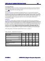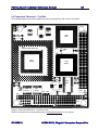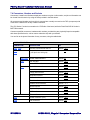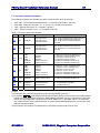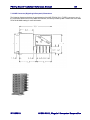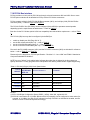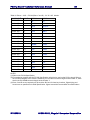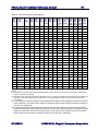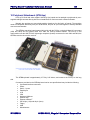
1
PC/II+p
Socket 7 Class Embedded Modular
Computer for Low-Power Applications
Technical Reference Manual
Please obtain copies of the Supplement and Addendum documents for PCpi specific
information. Supplement document gives an overview of changes that occur when
migrating to the megatel PCPi platform. The Addendum provides technical details of
options or features on the PCpi that were not offered on the PC/II+p.
Document Number: MT002615
Revision: 1.5
Version: Release
TERMS OF USE FOR THIS MANUAL
Those portions of this Manual (including this part) containing Notices of Copyright, Warranty, Intellectual Property,
Trademark Information and legal cautions may not be altered, concealed or deleted by anyone without the explicit
consent of Megatel in writing.
The information contained in this Manual may be used only for the purposes permitted by and subject to license
Agreements contained in this document and in other product documentation, in Web-Site legal notices and in
Confidentiality Agreements governing the disclosure and use of this information. This Manual is provided to the User for
informational purposes only. The User may use a single copy of this Manual for their personal use only, and the User
may not reproduce, modify and create derivative works to this Manual without the written authorization of Megatel.
LIMITED WARRANTIES
Megatel makes no representation or warranty with respect to any circuitry or software not embedded within a Megatel
Product.
Megatel warrants that for a period of one (1) year, beginning on the date that Megatel ships a Megatel product, the thencurrent documentation and specifications will materially conform to the Hardware and Software contained therein and will
operate in accordance with Megatel's published specifications and documentation for that product at the date it is
shipped, provided that the user’s sole remedy and Megatel's sole liability for breach of this warranty shall be to return
any defective Megatel Produce for replacement or repair or (if such replacement or repair is not economically feasible
then, at Megatel’s election) for credit to the User. The User is responsible for all costs associated with return freight and
insurance to (and from) Megatel's designated location.
This LIMITED WARRANTY is contingent upon the proper use of the product. The WARRANTY is void if repairs are
necessary due to accident, unusual physical, electrical or electro-magnetic stress, misuse, shipping or causes other than
ordinary use including causes due to any user-supplied BIOS or other software if applicable. The WARRANTY is also
void if the Hardware product has been modified or disassembled, or if the serial number label on the Product is altered or
removed, or if any repairs or modifications are attempted by anyone not authorized by Megatel, or if any physical
modification is made to the factory-set configuration if applicable, or if any modification is made to the physical board,
without prior written permission from Megatel.
EXCLUSIVE WARRANTIES
THE FOREGOING WARRANTIES AND REMEDIES ARE EXCLUSIVE AND ARE IN LIEU OF ALL OTHER
WARRANTIES, EXPRESS OR IMPLIED, EITHER IN FACT OR BY OPERATION OF LAW, STATUTORY OR
OTHERWISE INCLUDING WARRANTIES OF MERCHANTABILITY, FITNESS FOR A PARTICULAR PURPOSE.
MEGATEL SHALL NOT BE LIABLE UNDER THIS WARRANTY IF THE ALLEGED DEFECT IN THE PRODUCT DOES
NOT EXIST OR WAS CAUSED BY USER'S OR ANY THIRD PERSON'S (FOR WHOM MEGATEL IS NOT
RESPONSIBLE AS PROVIDED HEREIN) MISUSE, NEGLECT, IMPROPER INSTALLATION OR TESTING,
UNAUTHORIZED ATTEMPTS TO REPAIR, OR ANY OTHER CAUSE BEYOND THE RANGE OF THE INTENDED
USE, OR BY ACCIDENT, FIRE, LIGHTNING OR OTHER HAZARD.
Megatel makes no Warranty or Representation about the accuracy of anything contained in this Manual, which is
provided to the User for informational purposes. The User shall make no claim in damages (including but not limited to
special, general, direct, indirect and consequential damages) or otherwise against Megatel arising from its use, or the
use by others, of this Manual.
Megatel Products are not designed for use in applications where they are relied upon for the protection and preservation
of human life, including such applications as control of aircraft, air traffic, aircraft navigation or aircraft communications,
or in the design, construction, operation or maintenance of any nuclear facility, or in the operation or maintenance of any
direct life support system. The products may have such applications but the parties making such use should assure itself
that all safety concerns are addressed fully. Megatel disclaims any express or implied warranty of fitness for such uses
in the absence of Megatel’s specific undertaking in writing in that regard.
COPYRIGHTS AND TRADEMARKS
No part of this document may be copied or reproduced in any form or by any means without prior written permission from
Megatel Computer (1986) Corporation. Entire contents Copyright © 1999-2000, Megatel Computer (1986) Corporation,
Toronto, Canada. Printed in Canada.
"megatel", PC/II+p, +p, "Mass I/O" are trademarks or registered trademarks of Megatel Computer (1986) Corporation
"Intel", "Pentium" are registered trademarks of Intel Corporation
"IBM", "XT" are registered trademarks of IBM Corporation
"Microsoft", "MS-DOS", "MS" are registered trademarks of Microsoft Corporation
All other trademarks are registered trademarks of their respective owners.
PC/II+p
Socket 7 Class
Embedded Modular
Computer for LowPower Applications
The PC/II+p board is a rugged full featured
PENTIUM or K6 SBC that has been engineered
with available leading edge components and
software. This board supports the available lowpower socket 7 processors, and utilizes the ALI
chipset which provides both PCI and ISA buses. It
is PC/104 compliant and 104Family I/O compliant.
This board is available with a broad set of options
that can be mixed in any combination to maximize
price and performance. On-board options include
your choice of processor, 69030-based Super VGA
& LCD output, Ethernet, Flash disk (Disk-on-Chip)
and 16 to 64 MB of soldered-down high-speed
SDRAM. Many other options and base features are
packed into this tiny board, all of which are
combined into a small rugged package that is
powered from a single 5V supply.
•
Megatel PC/II+p Board with Low Power Socket
7 Processor, on-chip L1 Cache, and ALI north
and south bridges with Local Bus Memory
•
Supports 66 MHz Bus and CPU Core Speeds
up to 266 MHz
•
32 MB to 64 MB of high-speed soldered down
SDRAM memory
•
8- or 16-Bit PC/104 Bus
•
165-Pin Mass I/O interface uses H.M. 2mm
IEC Connector System
•
AT Keyboard and PS/2-Style mouse
•
USB 12 Mbps, one hub & two ports
•
Intel (Chips) Advanced 69030 CRT and Flat
Panel Display Controller on the PCI Local Bus,
and 4 MB of Fast on-chip Video DRAM
memory
•
Crystal CS8900 Ethernet 10Base-T and AUI
Controller & Filters with on-chip RAM buffers,
and on-board Configuration EEPROM and
LEDs, and Header
•
ATA/IDE Ultra 33 Hard drive interface
•
Dual Serial 16C550 ports supports full RS-232
communications, 230K baud
•
Parallel Port ECP/EPP (1284 style)
•
Floppy Interface, Watchdog, Advanced Y2K
Real-Time Clock and all basic AT peripherals
•
256 KB Flash Bios (soldered) for Megatel
Custom 100% AT compatible bios and option
bios modules
•
Flash Disk Disk-on-Chip Socket (up to 144+
MB)
To Contact Us: Megatel Computer Corporation, 125 Wendell Ave, Weston, ON M9N 3K9, Canada
Tel:+1 416 245-2953 Fax:+1 416 245-6505 Toll Free: 1-888-SMALL-PC
Website: http://www.megatel.ca/ Email: [email protected]
PC/II+p Board Technical Reference Manual
4
Revision List
Page
REVISION MT002605 2000/02/02
Prerelease Version for PC/II+p v2.00
Manual reformatted
Component Top, Bottom & Dimension Diagrams updated
Component naming updated
Video Resolution, Colors, Refresh & Clocks Support updated
1ff
30, 31, 96
Various
n/a
REVISION MT002606 2000/04/25
Prerelease Version for PC/II+p v2.01
NOTE: As of PCB Version 2.01, the preliminary specification for the PC/II+p has been modified as follows:
- Changed the Supported Processors to one of the following:
(a) the Intel Low-Power Embedded Pentium Processor operating at 166 MHz or 266 MHz; and
(b) the AMD Embedded K6-2E Processor operating at 233 MHz.
- Changed the Video Controller to the Intel 69030 Advanced CRT/Flat Panel Accelerator,
which includes an on-chip high-speed 4 MB video memory
- Changed the main memory support to 1 or 2 banks of soldered SDRAM, 32 MB to 64 MB
- Changed the larger on-board power supplies to high-efficiency switching supplies that support
the required Core voltage (1.9V), and +3.3V; a small +2.5V I/O supply is also provided.
Please also NOTE that revision 2.01 of the PCB is PRE-PRODUCTION; therefore, the
SPECIFICATION CONTAINED HEREIN IS PRELIMINARY AND IS SUBJECT TO CHANGE.
Component Top, Bottom & Dimension Diagrams updated
Board Block Diagram updated
Bill of Materials updated
General corrections
30, 31, 96
20
28
Various
REVISION MT002606 2000/07/08
Prerelease Version for PC/II+p v2.01
NOTE: This revision of PCB Version 2.01 finalizes several issues related to functionality, including provision
of the panel ENAVEE polarity option which is included. Other issues relate to manufacture. PCB artwork for
copper thermal sink areas were also updated.
- Added the "panel ENAVEE polarity" option "c"
91
- Model number updated
88 - 93
- Option M (Memory) Code 0 (No Memory) deleted; Min of 32 MB SDRAM is required
91
- Added CRT Interface Signals table
73
- Added Panel Interface Signals table
74
REVISION MT002612 2000/10/28
Release Version for PC/II+p v2.02
NOTE: This revision of PCB Version 2.02 addresses several manufacturing issues. Except as noted below,
functionality, mechanical and electrical interfaces are unchanged.
- Memory supported (32 MB or 64 MB) options updated
3, 16, 51, 12, 25, 89, 91
- Certification requirement of CPU processors added
36
- References to M1543 changed to M1543C (step -B1 is used on this board)
Various
- Absolute Maximum Ratings updated
23
- DC Electrical Characteristics updated
25
- Drawings updated
20, 30, 31, 96
MT002615
©1999-2001, Megatel Computer Corporation
PC/II+p Board Technical Reference Manual
5
REVISION MT002613 2001/01/28
Release Version for PC/II+p v2.03
NOTE: This revision of PCB Version 2.03 provides full support for the Intel Embedded Low Power 266 MHz
processor.
Notice of new document MT004702, "Ethernet Appbook" added to Ethernet Section
Interrupt IRQ Map updated
DMA Channel MAP updated
Clarification on the use of the RSTSW# I/O Pin (Manual Reset Switch) Added
38
81
82
64,24
REVISION MT002614 2001/03/15
Release Version for PC/II+p v2.04
Additions and Corrections to this manual include the following:
Added Power Connector description and pinout
Added Fan Connector description and pinout
Added Connector Pinout index
Hyperlinks added for all connector reference IDs (eg. J907 jumps to definitions for J907)
PC/104 speed default setting changed to 8.25 MHz
Preface added
59
41
33
Various
54
11
REVISION MT002615 2001/03/20
Release Version for PC/II+p v2.04
Documentation changes include the following:
Enable/Disabling port 92h description
PC/104 SYSCLK (ISA) Clock Speed Values
Watchdog
NMI Register aliases 70h,72h and 71h,73h
USB is Memory mapped by Windows Drivers; I/O map entries removed
PCI Configuration registers (Address & Data DWORDs) in I/O space added
USB IRQ 11 Mapping added
MT002615
54
54
76-77
78
78
78
81
©1999-2001, Megatel Computer Corporation
PC/II+p Board Technical Reference Manual
Table of Contents
6
Page
1 INTRODUCTION................................................................................................................................12
1.1 PC/II+p Overview ........................................................................................................................12
2 REFERENCE DOCUMENTS.............................................................................................................14
2.1 Datasheets ..................................................................................................................................14
2.2 Reference Standards...................................................................................................................14
2.3 Other References ........................................................................................................................14
3 SPECIFICATION SUMMARY............................................................................................................15
3.1 PC/II+p Board Specifications.......................................................................................................15
3.2 PC/II+p Board Block Diagram .....................................................................................................20
4 SETTINGS .........................................................................................................................................21
4.1 Jumper Settings – Cpu Type and Clock Frequencies.................................................................21
4.2 Jumper Settings – Other .............................................................................................................22
5 ELECTRICAL SPECIFICATIONS .....................................................................................................23
5.1 Absolute Maximum Ratings.........................................................................................................23
5.2 Recommended Operating Conditions .........................................................................................24
5.3 DC Characteristics.......................................................................................................................25
5.4 Voltage Monitor ...........................................................................................................................26
5.5 PC/104 Bus Drive Current...........................................................................................................27
6 COMPONENT SUMMARY ................................................................................................................28
6.1 Bill of Materials ............................................................................................................................28
6.2 Component Placement – Top Side .............................................................................................30
6.3 Component Placement – Bottom Side ........................................................................................31
7 FUNCTIONAL SPECIFICATIONS ....................................................................................................32
7.1 Bridge ..........................................................................................................................................32
7.2 Bus, DRAM Memory, Peripheral Controllers...............................................................................32
7.3 Clock............................................................................................................................................32
7.4 Connectors, Headers and Sockets..............................................................................................33
7.4.1 Connector Sample Part Numbers.........................................................................................34
7.4.2 AMP Connector (Right-Angle Receptacle) Dimensions .......................................................35
7.5 Cpu Processor.............................................................................................................................36
7.6 Disk..............................................................................................................................................37
7.7 Ethernet Interface ........................................................................................................................38
7.7.1 Ethernet Interface Pinout ......................................................................................................39
7.8 Fan Connector – J008 .................................................................................................................41
7.8.1 Fan Connector – J008 – Pinout ............................................................................................41
7.9 Flash ROM – BIOS......................................................................................................................42
7.10 Flash Disk..................................................................................................................................43
7.11 Floppy Disk Interface.................................................................................................................44
7.11.1 Floppy Disk Interface Pinout...............................................................................................45
7.12 IDE / ATA Ultra 33 Interface......................................................................................................46
7.12.1 IDE Interface Pinout............................................................................................................47
7.13 Keyboard & Mouse Interface.....................................................................................................50
7.13.1 Keyboard Interface Pinout ..................................................................................................50
7.13.2 Mouse Interface Pinout.......................................................................................................50
7.14 Memory......................................................................................................................................51
7.15 Mouse........................................................................................................................................51
MT002615
©1999-2001, Megatel Computer Corporation
PC/II+p Board Technical Reference Manual
7
7.16 North Bridge ..............................................................................................................................52
7.17 Parallel Port ...............................................................................................................................52
7.17.1 Parallel Port Pinout .............................................................................................................53
7.18 PC/104 Bus Interface ................................................................................................................54
7.18.1 PC/104 Pinout.....................................................................................................................56
7.19 Power (+5V) Connector - J907..................................................................................................59
7.19.1 Power (+5V) Connector Pinout - J907................................................................................59
7.20 Processor ..................................................................................................................................59
7.21 Real-Time Clock ........................................................................................................................60
7.21.1 Real-Time Clock – Features ...............................................................................................60
7.21.2 Real-Time Clock – Setting Time and Date .........................................................................60
7.21.3 Real-Time Clock – Using the NVRAM ................................................................................60
7.21.4 Real-Time Clock – Interrupt 1Ah Functions........................................................................61
7.21.5 Real-Time Clock – Memory Map ........................................................................................62
7.22 Reset Switch..............................................................................................................................64
7.22.1 Reset Switch Interface Pinout.............................................................................................64
7.23 Serial Ports ................................................................................................................................65
7.23.1 Serial COM1 Pinout ............................................................................................................66
7.23.2 Serial COM2 Pinout ............................................................................................................67
7.24 South Bridge..............................................................................................................................68
7.25 Speaker Output .........................................................................................................................68
7.25.1 Speaker Interface Pinout ....................................................................................................68
7.26 Timers / Counters ......................................................................................................................69
7.27 USB Ports..................................................................................................................................70
7.27.1 USB Interface Pinout ..........................................................................................................70
7.28 Video – 69030 CRT & Panel Controller.....................................................................................71
7.28.1 Video Analog CRT Display Support....................................................................................71
7.28.2 Video Flat Panel Display Support .......................................................................................71
7.28.3 Video Mode Support – Standard VGA Modes....................................................................73
7.28.4 Video Mode Support – Extended Modes............................................................................73
7.28.5 Video CRT Interface – J903 ...............................................................................................73
7.28.6 Video Panel Interface – J904..............................................................................................74
7.29 Watchdog ..................................................................................................................................76
7.29.1 Watchdog Modes ................................................................................................................76
7.29.2 Watchdog functions ............................................................................................................76
7.29.3 WatchdogEnable() Function ...............................................................................................77
7.29.4 WatchdogDisable() Function ..............................................................................................77
7.29.5 WatchdogStrobe() Function................................................................................................77
8 SYSTEM RESOURCE MAPS ...........................................................................................................78
8.1 I/O Address Map..........................................................................................................................78
8.2 Memory Map – First Megabyte....................................................................................................80
8.3 Interrupt IRQ Map........................................................................................................................81
8.4 DMA Channel Map ......................................................................................................................82
9 MASS I/O CONNECTOR PINOUT ....................................................................................................83
9.1 Mass I/O Pinout ...........................................................................................................................83
9.2 Mass I/O Power & Ground Pins ..................................................................................................85
10 PERIPHERAL ATTACHMENT (QTB/DXP) ....................................................................................86
11 ORDERING INFORMATION ...........................................................................................................88
11.1 PC/II+p Product Numbering ......................................................................................................88
11.2 PC/II+p Specific Order Example................................................................................................89
11.3 PC/II+p Order Options...............................................................................................................90
MT002615
©1999-2001, Megatel Computer Corporation
PC/II+p Board Technical Reference Manual
8
11.3.1 Option a – Watchdog ..........................................................................................................90
11.3.2 Option b – Power Supply Arrangement ..............................................................................90
11.3.3 Option c – Panel ENAVEE Polarity.....................................................................................91
11.3.4 Option E – Ethernet ............................................................................................................91
11.3.5 Option H – Flash Disk.........................................................................................................91
11.3.6 Option K – Real-Time Clock & Battery ...............................................................................91
11.3.7 Option M – Memory, SDRAM .............................................................................................91
11.3.8 Option P – Processor..........................................................................................................91
11.3.9 Option S – Serial I/O...........................................................................................................92
11.3.10 Option V – Video...............................................................................................................92
11.3.11 Option X – PC104.............................................................................................................92
11.3.12 Option Y – MASS I/O 5X11 ..............................................................................................92
11.3.13 Option Z – MASS I/O 5X22...............................................................................................93
12 SERVICE INFORMATION ...............................................................................................................94
13 PHYSICAL SPECIFICATIONS........................................................................................................96
MT002615
©1999-2001, Megatel Computer Corporation
PC/II+p Board Technical Reference Manual
List of Figures
Figure 1
Figure 2
Figure 3
Figure 4
Figure 5
Figure 6
Figure 7
Figure 8
Figure 9
9
Page
PC/II+p Block Diagram (V2.04) .............................................................................................20
Component Placement – Top Side (v2.04) ...........................................................................30
Component Placement – Bottom Side (v2.04) ......................................................................31
Diagram – J905 – Ethernet 2x5 Pin .100 Inch R/A Male Header ..........................................39
Diagram – J901 – PC/104 (Rows A and B) – 2 X 32 .100" Header .....................................56
Diagram – J902 – PC/104 (Rows C and D) – 2 X 20 .100" Header .....................................56
Diagram – J907 – +5v Power Header ...................................................................................59
Diagram – MASS I/O J903, J904 (Rows A-E) – 5X11, 5X22 2-mm HM Connector .............83
PC/II+p Physical Dimensions (v2.04) ....................................................................................96
List of Tables
Page
Table 1 Jumper Settings – Cpu Type and Clock Frequencies ............................................................21
Table 2 Jumper Settings – Other .........................................................................................................22
Table 3 Electrical – Absolute Maximum Ratings..................................................................................23
Table 4 Electrical – Recommended Operating Conditions ..................................................................24
Table 5 Electrical – DC Characteristics ...............................................................................................25
Table 6 Electrical – Voltage Monitor Characteristics ...........................................................................26
Table 7 Electrical – PC/104 Bus Drive Current....................................................................................27
Table 8 Board Component List (v2.04) ................................................................................................28
Table 9 Connector Option Part Numbers.............................................................................................34
Table 10 Supported Processors List (v2.04)........................................................................................36
Table 11 Pinout – J905 – Ethernet 2x5 Pin .100 Inch R/A Male Header.............................................39
Table 12 Signals – J905 – Ethernet 10Base-T Interface .....................................................................40
Table 13 Signals – J905 – Ethernet AUI Interface...............................................................................40
Table 14 Signals – Fan J008 – 1x2 .100 inch Pin Header..................................................................41
Table 15 ETHERNET Drivers & Utilities ..............................................................................................42
Table 16 VIDEO Drivers & BIOS Options ............................................................................................42
Table 17 Signals – J904 – Floppy Disk Interface ...............................................................................45
Table 18 Signals – J903 – IDE/ATA Interface .....................................................................................47
Table 19 Signals – J904 – Keyboard Interface ....................................................................................50
Table 20 Signals – J904 – Mouse Interface.........................................................................................50
Table 21 Total System Memory Options..............................................................................................51
Table 22 Signals – J904 – Parallel LPT1 Interface..............................................................................53
Table 23 PC/104 SYSCLK (ISA) Clock Speed Values ........................................................................54
Table 24 PC/104 (ISA) Refresh Periods ..............................................................................................55
Table 25 PC/104 (ISA) 16-Bit Memory Wait States.............................................................................55
Table 26 PC/104 (ISA) 16-Bit I/O Wait States .....................................................................................55
Table 27 Pinout – J901 – PC/104 (Rows A and B) – 2 X 32 .100" Header ........................................56
Table 28 Pinout – J902 – PC/104 (Rows C and D) – 2 X 20 .100" Header........................................58
Table 29 Pinout – Power +5v J907 – 1x12 PIN .100" R/A Male Header.........................................59
Table 30 Real-Time Clock Memory Map .............................................................................................62
Table 31 RTC Extended RAM Memory Map .......................................................................................63
Table 32 Signals – J904 – Reset Switch Interface ..............................................................................64
Table 33 Serial Channel Baud Rates (From ALI M1543C Datasheet) ................................................65
Table 34 Signals – J904 – Serial COM1 Interface...............................................................................66
Table 35 Signals – J904 – Serial COM2 Interface...............................................................................67
Table 36 Signals – J904 – PC Speaker Output Interface ....................................................................68
Table 37 Signals – J904 – USB Ports 0 & 1 Interface .........................................................................70
Table 38 Flat Panel Interface Signal Mapping .....................................................................................72
Table 39 Signals – J903 – Video CRT Display Interface.....................................................................73
Table 40 Signals – Mass I/O J904 – Panel Interface...........................................................................74
Table 41 I/O Map .................................................................................................................................78
MT002615
©1999-2001, Megatel Computer Corporation
PC/II+p Board Technical Reference Manual
Table 42
Table 43
Table 44
Table 45
Table 46
Table 47
Table 48
10
Memory Map – First Megabyte .............................................................................................80
Interrupt Map.........................................................................................................................81
DMA Map ..............................................................................................................................82
Pinout – MASS I/O J903 (Rows A, B, C, D and E) – 5 X 11 2mm HM Connector ...............83
Pinout – MASS I/O J904 (Rows A, B, C, D and E) – 5 X 22 2mm HM Connector ...............84
Signals – Mass I/O J903,J904 – Power & Miscellaneous.....................................................85
QTB/dxp Connector List........................................................................................................87
MT002615
©1999-2001, Megatel Computer Corporation
PC/II+p Board Technical Reference Manual
11
Preface
This document uses hyperlinks to assist you in navigating.
In this document, hyperlink text is underlined - but color is normally black.
Underlining is not used elsewhere.
In some cases where, within a table, hyperlink text is also colored, the hyperlink text will not be black in that
case but, instead, reflect the color normally used in the table for the corresponding item.
MT002615
©1999-2001, Megatel Computer Corporation
PC/II+p Board Technical Reference Manual
12
1 Introduction
Thank you for your interest in the Megatel PC/II+p Cpu board, one of the 104Family of scalable complete
computer boards from Megatel. If you have chosen this board for your applications, you have chosen a
rugged, reliable high-performance and low-cost solution. This board has been engineered to be compatible
not only with other boards in the Megatel 104Family line, but also to the PC/104 industry standard for
embedded computer-based products.
This document has sections that are organized as follows: Reference Documents, Specification Summary,
Settings, Electrical Specifications, Component Summary, Functional Specifications, (which are presented
topical order), and System Resource Maps sections.
The remaining sections contain Mass I/O Connector Pinout, Peripheral Attachment (QTB/dxp), Ordering
Information, and Physical Specifications.
This document also includes specifications for all connector interfaces, a component bill of materials for the
major parts on the board, component placement templates, a functional specification for the board's various
peripheral support features, and a list of the options for the board including the jumpers and manufacture
options. Please feel free to contact Megatel or one of its distributors or agents if you require more
information.
1.1 PC/II+p Overview
The basic PC/II+p is PC/104 compliant in its form factor and electrical interfaces. As a member of the
Megatel 104Family, it is easily interchangeable with other members of the family to provide the feature set
and performance range you require. The PC/II+p provides on-board 8-Bit or 16-Bit PC/104 bus connectors to
allow direct drop-in compatibility with existing and new PC/104 designs.
The PC/II+p board is powered by a standard 296-pin or 321-pin Low-Power Socket 7 or compatible
Processor. The board supports processors from Intel (Low Power Pentium MMX 166 & 266) and AMD (K62E/233). The processor speed and voltage options are listed later in this document. The local 64-bit
processor bus operates at 66 MHz which directly interfaces to the ALI M1531B north bridge to provide an onboard 33 MHz PCI bus and memory controller. The ALI M1543C south bridge interfaces directly to the PCI
bus, generates a full ISA bus, and provides AT architecture and legacy peripheral support.
Soldered down SDRAM is provided to support from 32 MB up to 64 MB of high-speed (10 ns or better)
memory. One or two banks of soldered SDRAM can be populated.
The board also contains a 256 KB flash device to hold system BIOS, and optionally contains a 32-pin DIPtype socket that can be user-populated with a M-SYSTEM's Disk-On-Chip® or compatible device to provide
up to 144 MB or greater of Flash Disk memory.
A rich complement of peripheral controllers and interfaces in included. Optional Full Video is provided by the
Chips & Tech advanced 69030 controller that supports simultaneous CRT and a wide variety of 8/16/24-Bit
flat panels. Optional Ethernet is provided by the Crystal CS8900 controller with integrated frame buffer
memory and filters, and on-board transformers support either or both 10Base-T and AUI Ethernet interfaces.
An Ultra-33 ATA/IDE controller (provided by the M1543C south bridge) supports a primary controller with up
to four devices. AT-style Keyboard, PS/2-style mouse, and Floppy are provided by the M1543C south bridge.
Up to 2 full RS-232 Serial ports are also provided with optional on-board RS-232 Transceivers for all
standard RS-232 signals. A USB hub that supports two USB ports is supported by the M1543C, using either
FS (12 Mbits/Sec) or LS (1.5 Mbits/Sec). An up-to-date Y2K Real-Time Clock controller is provided, the
Dallas DS1685 that provides extended alarm and interrupt generation features, extended NVRAM, a unique
silicon serial number and other extended features.
MT002615
©1999-2001, Megatel Computer Corporation
PC/II+p Board Technical Reference Manual
13
All peripheral I/O, including Video CRT, 24-Bit Flat Panel, Keyboard, Mouse, IDE, 2 Serial and Parallel ports
are pulled to a Mass I/O Connector on the board. The Ethernet is provided separately on a standard 2x5 pin
header. A 12-pin power header is provided to supply the single +5V rail to the board and the +5V rail is
regulated to +3.3V, +2.5V and the CPU Core Voltage (+1.9V typical) by two on the board high-efficient
switching regulators and a tiny linear regulator. On-board voltage monitors are provided to manage power
levels, and a hardware-enabled software-controlled Watchdog is available on the board.
The on-board core BIOS is contained in a 256 KB flash ROM which is configured and shadowed into
conventional system RAM at boot time. The flash ROM also contains option BIOS modules (for example, the
Chips/Intel Video bios) which may be loaded into conventional system RAM at boot time depending upon
options ordered with the board. The BIOS is fully AT compliant.
The FR4 PCB is manufactured to megatel technology standards, and was routed to a minimum number of
layers. It uses a separate ground plane and multiple power planes to provide a controlled impedance
environment for the high-speed operation of the board. The board template specification is given later in this
document. The on-board power monitors tightly hold the board in RESET state while power is ramping up or
down outside of the ±5% operating range and until all clocks are stable.
PC/II+p uses up-to-date low-cost components and provides a powerful SBC engine. Careful engineering was
used throughout its design to provide robust operation. Compared to conventional PC/104 Cpu boards, the
PC/II+p provides a unique solution that combines high performance, very high density and low cost. The
board is offered in its base configuration that consists of minimal memory, system controller and CPU. All
options are orthogonal and any combination of peripherals can be populated and custom performance
settings can be ordered at your option to meet your price/performance requirements.
For scalable designs, the Pc/II+p and the other 104Family members offer you a solution with an excellent
combination of a low-cost and high-tech engineered performance.
MT002615
©1999-2001, Megatel Computer Corporation
PC/II+p Board Technical Reference Manual
14
2 Reference Documents
2.1 Datasheets
Acer Laboratories Inc.
Aladdin IV – M1531B Cpu-to-PCI bridge, Memory, Cache and Buffer Controller
Data Sheet, Version 1.2, Jan 1998
Acer Laboratories Inc.
Aladdin – M1543 Desktop South Bridge Datasheet, Version 1.25, Jan 1998
AMD
AMD-K6-2E Embedded Processor Datasheet, Advanced Micro Devices, Pub#
22529, Revision B/0, January/2000.
Analog Devices
EMI/EMC Compliant ±15 kV ESD Protected RS-232 Line Drivers/Receivers
(ADM211E), 1996
Chips/Intel
69030 Databook, Dual HiQVideo Accelerator with 4MB Embedded Memory,
Revision 1.3, November 24,1999; Pub# DB182.3, Stock# 010-182-003
Chips/Intel
69000 HiQVideo Series Application Note Book, Revision 1.1, December 4,
1998; Pub# AN119.1; Stock# 020119-001
Crystal Semiconductor Corp CS8900 Highly Integrated Ethernet Controller Datasheet, DS150PP2, Dec 95
Crystal Semiconductor Corp Crystal LAN CS8900 Ethernet Controller Technical Reference Manual,
AN83REV1, Version 1.31, Sep 1996
Dallas Semiconductor
DS1706S 3.3V and 5.0V MicroMonitor Datasheet, Feb 1998
Dallas Semiconductor
DS1685 Real Time Clock Datasheet, Mar 1998
Intel
Low-Power Embedded Pentium Processor with MMX Technology Datasheet,
Order Number 273184-003, September/1999
Intel
Extended Temperature Pentium Processor with MMX Technology Datasheet,
Order number 273232
Intel
Embedded Pentium Processor Family Developer's Manual, Order Number
273204
Pulse/Valor
ST7010 10Base-T Transformer Datasheet, Rev C
Pulse/Valor
Ethernet AUI Transformers (ST7033) Datasheet, E/AUI105-01, Nov 1995
2.2 Reference Standards
Annabooks
ANSI
ANSI
IEEE
IEEE
Intel
Intel
PC/104 Consortium
PCI Special Interest Group
AT Bus Design IEEE P996-Compatible, Edward Solari
AT Attachment with Packet Interface Extension (ATA/ATAPI-4), ANSI X3.297,
1997
BIOS Enhanced Disk Drive Specification (EDD), T13/1226DT
P996.1 Standard for Compact Embedded-PC Modules
IEEE 1284 Extended Capabilities Port Protocol and ISA Standard, Revision
1.09, Jan 1993
Socket 5 Specification – Pentium Processor Family Developer's Manual,
Volume 1: Pentium Processors, Order number 241428; Chapter 32
Socket 7 Specification – Pentium Processor Family Developer's Manual, 1997;
Chapter 17
PC/104 specification – Revision 2.3 – June 1996
Small PCI Specification, Version 1.0, May 1996
2.3 Other References
Microsoft Press
Annabooks
MT002615
The Programmer's PC Sourcebook, Thom Hogan
PCI Hardware and Software, Architecture & Design, Edward Solari & George
Willse, 4th Edition, 1998
©1999-2001, Megatel Computer Corporation
PC/II+p Board Technical Reference Manual
15
3 Specification Summary
3.1 PC/II+p Board Specifications
Board Form Factor:
Board Type:
3.775 x 3.550 inch, PC/104 compliant
FR4
Architecture:
PC®/AT
Central Processing Unit:
CPGA 321-Pin Socket, for Low-Power "Socket 7" or Compatible Processor
Accepts 321-Pin CPGA Processors or 296-Pin SPGA Low-Power
Processors (from Intel or AMD – see below for supported processors)
Full Socket 7 Compliance.
Intel Low-Power Pentium MMX Processor (166 Mhz and 266 MHz)
Local Bus Speed – 66 MHz
Superscalar (Pipelined) Architecture
32-Bit Cpu with 64-Bit Data Bus
Dual Pipeline
Integrated Pipelined Floating-Point Unit
Integrated Pipelined MMX Unit
Cache – Separate 16 KB Write-Back Data and 16 KB Code Caches
Voltages – Core 1.9V; I/O 2.5V
Package – PPGA-296
AMD K6-2E Embedded Processor (AMD-K6/-2E/233AMZ – 233 MHz)
Local Bus Speed – 66 MHz
Superscalar (6-Stage Pipelined) Architecture
10 Parallel Execution Units, 2-Level 8192-Entry Branch Prediction,
Out-of-Order Execution, Speculative Execution, Register Renaming
Integrated Pipelined Floating-Point Unit (IEEE 754/854)
Integrated Pipelined MMX Unit
Cache – Separate 32 KB Write-Back Data and 32 KB Code Caches
Decode Cache – 20 KB
Branch-Target Cache – 8K-Entry
Package – CPGA-321
Voltage – Core 1.9V; I/O – 3.3V
Cache Memory:
L1 On-Chip Cache
32 KB or 64 KB – Separate Code/Data Organization
High performance write-back
Type of Cache and Additional Caching depends upon Processor
DMA:
(7) Channels, 32-Bit addressing
Four 8-Bit Channels, Three 16-Bit Channels
Provides compatible DMA transfers
Provides Type F transfers
Timer/Counters:
AT-compatible (8254 type) timers
for System Timer, Refresh Request and Speaker Output Use
MT002615
©1999-2001, Megatel Computer Corporation
PC/II+p Board Technical Reference Manual
16
PC Speaker Output:
Available on Mass I/O connector
Memory Bus:
Address Bus:
64-Bit Data bus
32-Bit Address bus
Power Monitoring:
Dual 5% monitor – 5V rail and on-board 3.3V
Reset hold time – 130 ms minimum, 200 ms typical
Transient voltage immunity
Manual Reset:
Available on Mass I/O Connector
Debounced, generates minimum of 130ms reset on Low to High
Initiated by pulling Manual Reset signal line Low, then High
Memory:
SDRAM (soldered) memory
Minimum System Memory 32 MB (soldered SDRAM)
Maximum System Memory 64 MB (soldered SDRAM)
SDRAM – 66 MHz (10 ns) typical
Memory Options:
SDRAM Soldered-down: 32 or 64 MB
Keyboard:
Mouse:
PS/2-style Keyboard supported
PS/2-style Mouse supported
Printer/Parallel Port:
(1) Full ECP / EPP / PS2 / SPP / 1284-style Parallel Port supported
Supports Standard mode
Supports IBM PC/XT, PC/AT and PS2 Bi-directional mode
Supports Enhanced mode
Supports Enhanced Parallel Port (EPP) mode
Supports High Speed mode
Supports Extended Capabilities Port (ECP) mode
Includes Protection Circuit (Printer Powered Up or at higher voltage)
Serial/RS232 Ports:
(1) or (2) high performance 16550-compatible UARTs
16-byte Send/Receive FIFOs
Supports baud rates to 460 K-baud using 24 MHz Clock Divided by 13
(1.8462 MHz reference is divided by Divisor to generate
16x Clock)
Full EIA-RS232E and CCITT V.28 Transceivers included
Output swing ±9V with all Transmitter Outputs
loaded with 3K ohms to Ground
ATA/IDE Hard Drives:
Integrated 2-Channel Dedicated PCI IDE Ultra 33 Master Controller
Supports up to 4 IDE devices
Supports Ultra 33 Sync DMA mode transfers up to 33 MBytes/S
Supports DMA Mode 2 Timing
Supports PIO Modes up to Mode 5 Timing
Supports Multiword DMA Mode 0,1,2 with independent timing
- 4 Drives
Supports dedicated Pins of ATA interface for Each Channel
Flash Disk:
Socket for user-supplied solid-state disk (32 Pin DIP)
Supports M-System Disk-on-Chip®
(up to 144 MB or greater of flash disk memory module, user-populated)
MT002615
©1999-2001, Megatel Computer Corporation
PC/II+p Board Technical Reference Manual
17
Video CRT & Flat Panel:
Intel 69030 HiQVideo Accelerator
VGA register set compatibility and I/O accessibility
Includes On-Chip SDRAM
4 MB of high-speed SDRAM for video buffer
Memory SDRAM operation at 83 MHz
Memory SDRAM transfers up to 664 MBytes/sec
Supports Analog CRT RGB Video Interface
Supports 24-Bit Flat Panel Interface
Flexible Panel Interface – TFT/MIM, DSTN, SSTN, EL, Plasma
Supports Mono and Color
Supports VGA, SVGA, XGA, SXGA, UXGA resolutions
Supports Quarter VGA 32-x240, 320x200
Supports 16:9 Aspect Ratio Panels, 1024x600
Supports Panel Power On/Off Sequencing
Supports HiQColor Technology
Up to 16.7M Colors on STN LCDs and 24-bit active matrix LCDs
256 Gray Shades
Support for Dot Clock to 170 MHz
Support for Flexible Display Modes
Single View Mode – up to 1600 x 1200 x 16 bpp at 60 Hz refresh
Dual Independent Mode - up to 1280 x 1024 x 8 bpp at 60 Hz
refresh
Supports Simultaneous CRT / Flat Panel operation
Supports Graphics Acceleration
64-bit Single Cycle BitBLT Engine
Many Features
Supports panels from popular manufacturers
such as Sharp, Optrex, Toshiba, Hitachi, Fujitsu, Samsung,
NEC, Sanyo and others
Chips/Intel drivers & Option BIOS included
Ethernet:
Crystal CS8900 High-performance 10Base-T and AUI controller option
IEEE 802.3 compliant MAC engine, full duplex operation
On-chip RAM buffers – for Transmit & Receive frames
AUI port for 10Base-2, 10Base-5 and 10Base-F
10Base-T filters included
10Base-T and AUI isolation transformers are included
10Base-T port has automatic polarity detection and correction
Auto negotiation function
LED for inbound/outbound frames to/from local controller included
LED for either valid 10Base-T link present, or other general function
Floppy Disk:
Integrated Floppy Disk Controller – 2.88 MB (formatted)
Compatible to PD765A and 82077SL Architecture
Supports two 16-byte data FIFOs
Supports two (2) 3.5" floppy disk drives
Supports 3.5" FDD modes – 720 KB / 1.2 MB / 1.44 MB
Supports 1 Mbps / 500 Kbps / 300 Kbps / 250 Kbps data transfers
Supports swappable Drives A and B
Real-Time Clock, Alarm:
Dallas-Certified DS1685 – Y2K Real-Time Clock Controller
Periodic Interrupt Generator – settable from 122 us to 500 ms
Alarm Interrupt Generator – settable to any time 24 hour period
242-byte NVRAM included
12 or 24 hour format
MT002615
©1999-2001, Megatel Computer Corporation
PC/II+p Board Technical Reference Manual
18
Daylight savings time support
Unique 48-Bit Serial Number can be used for customer application
Watchdog:
Dallas DS1706 with Watchdog
Hardware timer is strobed once per second or faster
Hardware timer expiry issues system RESET
Hardware disable function via jumper
Software BIOS Disable, enable and strobe functions
USB
Integrated controller supports one root hub with two USB ports
Supports OpenHCI 1.0a specification
Supports FS (12 Mbits/Sec) serial transfers
Supports LS (1.5 Mbits/Sec) serial transfers
Supports legacy keyboard and mouse software with USB keyboard and
mouse
Connectors:
Power Connector (1) standard 1x12 right-angle header (+5V)
PC/104 Connectors (1) 2x32 and (1) 2x20 pin and socket header
stack-through and non stack-through
board stacking or other arrangements are customer specified
Ethernet Header (1) 2x10 right-angle header or customer specified
Mass I/O Connectors (1) 5x22 and (1) 5x11 IEC 2mm HM, or customer specified
total of 5x33 2mm grid
AMP Z-PACK 2mm HM Connector System
Type B22 and C
Support all variations straight and right-angle
male and female
Support top mounting (bottom by request)
Support 2mm headers on request (including board stacking headers)
IEC917 and IEC1076-4-101 compliant
All connectors except for Power are optional
Sockets:
(1) 321-Pin CPGA ZIF P55C (Low-Power) Socket-7 Processor Socket
(1) 32-Pin DIP Socket for Flash Disk compatible to M-System MD2200
Peripheral I/O Signals:
Signal Pins – Mass I/O Connector, PC/104 Headers and Ethernet Header
Signal Pins
Ethernet 10Base-T – 4
Ethernet AUI – 6
Ethernet LEDs – 2 (on-board dual LEDs)
Floppy Disk Bus – 15
IDE/ATA Bus – 28
Keyboard – 2
Mouse – 2
Parallel I/O – 17
PC/104 8-Bit Bus – 64
PC/104 16-bit Bus Extension – 40
Reset Switch – 1
Serial COM1 – 8
Serial COM2 – 8
MT002615
©1999-2001, Megatel Computer Corporation
PC/II+p Board Technical Reference Manual
19
Speaker Output – 1
USB port A – 2
USB port B – 2
Video Analog (CRT) – 5
Video Panel Interface (24-bit) – 32
Power & Ground
Supply Voltage:
Supply Power Rating:
Supply Regulation:
+5V Max Rise Time:
Single supply at +5V 5%
+5V Supply requires regulation to within 5%
(+3V to +5V) required within 100 ms
Storage Temperature:
Operating Temperature:
-50C to +125C, battery excluded
Commerical 0C to +70C standard
Industrial -20C to +85C : please call megatel for availability
Industrial -40C to +85C : please call megatel for availability
Operating Software:
Application Software:
Bios Software:
DOS, Windows, Windows 95, Windows NT4.0
x86 compatible
256 KB Flash EEPROM for Bios
Bios write protection (hardware)
Chips & Technologies 69030 VGA Driver BIOS included
AT compatible BIOS and Architecture
MT002615
©1999-2001, Megatel Computer Corporation
PC/II+p Board Technical Reference Manual
20
3.2 PC/II+p Board Block Diagram
For a description of component reference identifiers in the diagram, see section 6.1.
LOW-POWER SOCKET 7 CPU (SUCH AS AMD K62E, OR INTEL PENTIUM MMX)
POWER
MONITOR
CENTRAL
U2
L1
CACHE
16-64 KB
PROCESSOR
FPU
MMX
LOCAL BUS - 64-BIT / 66 MHZ
i
NORTH
BRIDGE
M1531B
RESET
SWITCH
DRAM
CONTROLLER
(M1531B)
SDRAM
16 - 64 MB
PCI BUS - 32-BIT / 33 MHZ
J904
USB HUB
CONTROLLER
(M1543)
USB (2)
IDE MASTER /
ULTRA 33
CONTROLLER
(M1543)
VIDEO PANEL
ACCELERATOR
69030
HIGH-SPEED
ON-CHIP 4 MB
VIDEO DRAM
J903
(4) IDE
PC104 BUS
J8
J904
SOUTH
BRIDGE
M1543
FLAT PANEL
J903
ISA BUS - 16-BIT
J901,J902
MONITOR
10BASE-T
J905
ETHERNET
CONTROLLER
CS8900
FLASH
BIOS
256 KB
EEPROM
1 KBIT
AUI
LEGACY I/O
CONTROLLER
(M1543)
WATCHDOG
RTC
U6
FLASH DISK
2 - 144 MB
J903,J904
SPEAKER
LPT1
ECP/EPP
COM1, COM2
AT KEYBOARD
PS/2 MOUSE
3.5"
FLOPPY
Figure 1 PC/II+p Block Diagram (V2.04)
MT002615
©1999-2001, Megatel Computer Corporation
PC/II+p Board Technical Reference Manual
21
4 Settings
4.1 Jumper Settings – Cpu Type and Clock Frequencies
Refer to Section 6.2 for the Component Placement – Top Side diagram. All jumpers are normally on the TOP
side of the board. This table applies only to jumpers J003, J004, J005, and J006. These jumpers are
populated as required by the processor option that you select. If 'no processor installed' is selected for the
processor option, the user should install the processor and set these jumpers as indicated in the table which
follows.
Please READ the notes at the end of this table.
Table 1 Jumper Settings – Cpu Type and Clock Frequencies
J003
J004
J005
J006
CPU
CORE
(MHz)
LOCAL
BUS
(MHz)
PCI
BUS
(MHz)
SUPPORTED PROCESSOR
open-x
open
open
open
166.6
66.6
33.3
AMD K6-2E/166
closed
open
closed
closed
closed
closed
open-x
open-x
166.6
266.6
66.6
66.6
33.3
33.3
INTEL FV-80503CSM-66/166 (SL27X)
INTEL FV-80503CSM-66/266 (SL274)
All other combinations
Not Supported
Reserved
NOTES:
(0) This table is preliminary; Contact Megatel to obtain a list of supported processors.
(1) Terminology used in table above:
open: shunt not installed
open-x: shunt normally not installed, or jumper may not be populated
closed: shunt installed
(2) Not all models or frequencies, that are supported by some of the processors, are supported by the
PC/II+p.
(3) The board will be shipped with jumpers specified above unless a custom processor or no processor is
ordered, in which case the jumpers should also be specified when the board is ordered. If you require
additional assistance in that case, please contact Megatel Engineering.
(4) Please be forewarned of the following:
– Megatel recommends you use ONLY a supported processor and a supported combination of
jumpers.
– The board must be equipped with a heatsink fan combination, or be externally cooled using a crossflow type of cooling arrangement which is appropriate for BOTH the speed of the host bus and Cpu
frequency selected, AND the environment within which the board is operating. Please specify the
intended operating speed range of the board to megatel when ordering this board to ensure that the
board is equipped with the appropriate heatsink fan combination. Do NOT operate the Cpu and/or Bus at
a speed beyond which it was designed to be operated and within the ranges indicated as Reserved.
– Before any of the Clock Frequencies jumpers are changed, ensure that the board is being supplied with
sufficient power to accommodate the increased speed of the Host Local Bus and the CPU Processor. Do
NOT operate the CPU and/or Bus at a speed beyond which it was design to be operated and within the
ranges indicated as Reserved.
MT002615
©1999-2001, Megatel Computer Corporation
PC/II+p Board Technical Reference Manual
22
4.2 Jumper Settings – Other
Refer to Section 6.2 for placement of Jumpers. All jumpers are normally on the TOP side of the board.
Table 2 Jumper Settings – Other
JUMPER
SETTING
SELECTED OPTION
COMMENT
J009
open
External bios
Used by Megatel manufacturing only
closed
Normal operation
(default)
Jumper must be present for normal
operation
open
Normal operation
(default)
closed
Program bios
Used by Megatel manufacturing only
open
Watchdog disabled
(default)
closed
Watchdog enabled
This option can be ordered; please refer
to section 11.3.1. The watchdog
controller and its internal functionality
will always operate, whether or not this
jumper is installed. However, the
system will ONLY be forced into reset
state at the time of a watchdog timer
expiry if the watchdog is enabled, the
timer has expired and this jumper is
INSTALLED.
open
Normal operation
(default)
closed
Reset RTC CMOS memory
This function is required to be enabled
by the BIOS. Before closing (installing)
this jumper, VCC Power may be
present or not present. When the
jumper is installed and the function has
been enabled by the BIOS, the contents
of the RTC NV SRAM User memory
(242 bytes used for system
configuration) is cleared. The jumper is
required to be removed before power is
applied (if power is applied when the
jumper is installed, remove the jumper
and then cycle the power to restore
operation). On reboot, default
configuration parameters are restored
by the BIOS.
J010
J014
J019
MT002615
©1999-2001, Megatel Computer Corporation
PC/II+p Board Technical Reference Manual
23
5 Electrical Specifications
The PC/II+p operates on a single +5V ± 5% supply. Power is supplied to the board through J907, the +5V
Power Connector. On-board power requirements at +3.3V, +2.5V and VCPUCORE are generated on-board,
using regulators (dual switching supplies provide +3.3V and VCPUCORE voltages). The board contains a
split power plane, two dedicated power planes, and a dedicated ground plane. A power supervisor with a
dual voltage monitor controls on-board RESET (POWERGOOD) signals during power ramp states.
The PC/II+p board sources +5V to the PC/104 bus. Other PC/104 bus voltages (-5v, +12v and -12v) are not
connected from the bus to the board.
The PC/II+p board sources +5V @3.0 A and +3.3V @50 mA to the MASS I/O connector, for use by optional
transition (QTB) connector boards Transition boards may be designed to be supplied only from the PC/II+p
Cpu board through the Mass I/O connector; or they may be directly supplied with external power; or they
may be supplied from both sources.
5.1 Absolute Maximum Ratings
Table 3 Electrical – Absolute Maximum Ratings
Parameter
Symbol
Min
Max
Units
Digital
VCC
-0.3
6.0
V
Power Supply Current
(Except
Peripherals)
ICC
Ambient Temperature
(Power Applied)
TA
-55
TS
-65
Power Supply
Storage Temperature
NOTES
mA
(3)
+125
°C
(1)
+150
°C
(2)
Current "from" CPU board
VM
3000
mA
(4)
"to" QTB board (Through
Mass I/O Connector)
Warning: Operation at or beyond these limits may result in permanent damage to the board or to
components attached to the board. Always operate the board at the Recommended
Operating Conditions, see below.
NOTES
(1) Temperature is given for a board for which a Battery is NOT included onboard (an order option). If the
board contains lithium battery, then the absolute temperature board ratings must be modified to meet the
more restrictive ratings for lithium batteries. Refer to manufacturer's specifications for Lithium Batteries.
Never exceed the ratings of a lithium battery if a battery is present on the board.
(2) Temperature is given for a board for which power is NOT applied and a Battery is NOT included onboard
(an order option). If the board contains a lithium battery, then the absolute temperature board ratings must
be modified to meet the more restrictive ratings for lithium batteries. Refer to manufacturer's
specifications for Lithium Batteries. Never exceed the ratings of a lithium battery if a battery is
present on the board.
(3) The maximum current specification refers to the maximum current through +5V Power connector, J907
using a board populated with all options, and assumes that each component on the board is
simultaneously pulling the manufacturer's maximum specified power.
(4) Specifies power supplied from the CPU board "to" the Transition Board. Note that power MUST NOT be
supplied to be CPU board through the Mass I/O connector – It must be supplied to the board from
an external source, through the standard Power connectors provided on the board.
MT002615
©1999-2001, Megatel Computer Corporation
PC/II+p Board Technical Reference Manual
24
5.2 Recommended Operating Conditions
Table 4 Electrical – Recommended Operating Conditions
Parameter
Power Supply
Power Supply Rise Time
Operating Ambient
Temperature
Digital
Symbol
Min
Typical
Max
Units
VCC
4.75
5.0
5.25
V
100
ms
+70
°C
(1)
+125
°C
(2)
+3.0V to +5.0V
SVCC
(Power Applied)
TA
0
TS
-55
Storage Ambient
Temperature
20.0
Humidity
(Untested)
HA
10
90
% RH
MR-RSTSW# Input Level
Low Level
RSTSWL
-0.03
+0.5
V
NOTES
(3)
High Level RSTSWH
+2.8
+3.6
V
(3)
MR-RSTSW# Input Level
NOTES
(1) Temperature is given for a board for which a Battery is NOT included onboard (an order option). If the
board contains lithium battery, then the absolute temperature board ratings must be modified to meet the
more restrictive ratings for lithium batteries. Refer to manufacturer's specifications for Lithium Batteries.
Never exceed the ratings of a lithium battery if a battery is present on the board.
(2) Temperature is given for a board for which power is NOT applied and a Battery is NOT included onboard
(an order option). If the board contains a lithium battery, then the absolute temperature board ratings must
be modified to meet the more restrictive ratings for lithium batteries. Refer to manufacturer's
specifications for Lithium Batteries. Never exceed the ratings of a lithium battery if a battery is
present on the board.
(3) Connector J904, pin MR-RSTSW# (the RSTSW# input pin) drives the Dallas DS1706 Reset Switch pin.
The DS1706 VCC is operated at +3.3V, and therefore the limits specified in the above table apply to
the PC/II+p and must NOT be exceeded. For compatibility to other Megatel 104Family boards, however,
and in accordance with Dallas recommendations, Megatel highly recommends that the RSTSW# line be
tied to GROUND to force a reset, and otherwise be left open; in the latter case, an internal 40K resistor in
the Dallas DS1706 chip pulls up the Manual Reset Switch pin to a high level during normal operation of
the board.
MT002615
©1999-2001, Megatel Computer Corporation
PC/II+p Board Technical Reference Manual
25
5.3 DC Characteristics
Table 5 Electrical – DC Characteristics
Parameter
Power Supply
Power Supply Current
Symbol
Min
Typical
Max
Units
(digital)
VCC
4.75
5.0
5.25
V
+5V Supply
ICC5
Power
PDD5
1.1A
NOTES
A
(1),(2)
W
(1)
Over Recommended Operating Conditions
NOTES
(1) Power requirements will vary depending upon the Cpu speed, amount of main memory and other options
chosen. Instantaneous power is also a function of the application[s] being run at any point in time.
Minimum Configuration – Pentium 166, Bus 66 MHz, 32 MB SDRAM, Flash Bios, K/B, Mouse, IDE,
Floppy, Real-Time Clock, Parallel Port;
Typical Configuration – Pentium 166, Bus 66 MHz, 32 MB SDRAM, Flash Bios, Video, K/B, Mouse,
IDE, Floppy, Real-Time Clock, Parallel Port, Serial Port;
Maximum Configuration – AMD 233 MHz, Bus 66 MHz, 64 MB SDRAM, Flash Bios, Flash Disk 144
MB, Ethernet 10Base-T & AUI, Video, K/B, Mouse, IDE, Floppy, Real-Time Clock, Parallel Port, 2 Serial
Port, USB Hub and 2 USB.
(2) Please contact Megatel for the latest Power information.
MT002615
©1999-2001, Megatel Computer Corporation
PC/II+p Board Technical Reference Manual
26
5.4 Voltage Monitor
A MicroMonitor is included on the board, the Dallas Semiconductor DS1706S, to provide both a watchdog
function and a dual-voltage monitor function. This section discusses the voltage monitor function; refer to
section 7.29 for a description of the watchdog function.
+3.3V Monitor
The +3.3V power supply is monitored by the DS1706S. When the +3.3V power supply falls below the
minimum Vcc tolerance (2.85v to 3.00v), the RST# output of the part is pulled low for a minimum of 130ms.
The RST# output is tied to the PC/II+p POWERGOOD signal that signals a reset to the board. The DS1706S
part's power supply voltage detection tolerance (2.85v to 3.00v) provides a minimum of 10% variation in the
+3.3V power supply, and a maximum of 15% variation in the +3.3V power supply. Megatel generates +3.3V
from the upstream supply (+5V) regulated to within 5% of +3.3V, which meets the requirements of
components on the board.
+5V Monitor
The upstream +5V power supply is monitored as well by the DS1706S. When the IN pin falls below the
minimum IN trip point (Vtp) tolerance (1.20v to 1.30v), the NMI# output of the part is pulled low. Because The
NMI# output of the part is tied to the RBRST# input of the part, the part pulls the RST# output of the part low
for a minimum of 130ms. The RST# output is tied to the PC/II+p POWERGOOD signal that signals a reset to
the board. A 1% precision voltage divider allows sense of the +5V supply using the IN pin of the part, and is
set to allow the +5V supply to drop to a minimum of 4.53V before tripping. The trip range, allowing for
tolerances, is 4.05V to 4.53V. Megatel recommends that the board should be operated with +5.0V on
the board, and in no case should the +5V supply be allowed to drop below 5% of its nominal value.
Other voltage planes on the board are regulated locally from the +5V supply rail.
Table 6 Electrical – Voltage Monitor Characteristics
Parameter
DS1706 VCCM
Symbol
Min
Typical
Max
Units
VCCM
3.15
3.3
3.45
V
VCCM Trip Point DS1706
(+3.3v
monitor)
VCCTP
2.85
2.93
3.00
V
IN - VCC5 Input Trip Point
(+5v
monitor)
VTP
4.05
4.29
4.53
V
Reset Active Time
TRST
130
205
285
ms
VCC Detect to RST and RST#
TRFP
130
204
285
ms
PBRST# Stable Low to RST
and RST#
TDLY
250
ns
VIN Detect to NMI#
TIPD
8
µs
5
Over Recommended Operating Conditions
MT002615
©1999-2001, Megatel Computer Corporation
PC/II+p Board Technical Reference Manual
27
5.5 PC/104 Bus Drive Current
The PC/104 bus drive current is specified by the PC/104 Specification, Version 1.3, listed in section 2.2. The
PC/II+p board complies to this standard. Most PC/104 bus signals have a reduced bus drive requirement of 4
mA. The 4 exceptions are open collector driven signals, which must drive 330-ohm pullup resistors defined
by the P996 specification.
The following signals must be driven with devices capable of providing 20 mA sink current:
MEMCS16#, IOCS16#, MASTER# and ENDXFR#.
All other signals may be driven with devices capable of providing 4 mA sink current. The following table of
source and sink currents apply to devices attached to the PC/104 (ISA) bus connector for the PC/II+p:
Table 7 Electrical – PC/104 Bus Drive Current
Symbol
IRQ[15:14], IRQ[11:9], IRQ[7:3]
RESETDRV
SD[15:8]
SD[7:0]
SA[19:17]
SA[16:0]
SBHE#
LA[23:17]
IOCS16#
MEMCS16#
MEMR#
MEMW#
AEN
IOCHRDY
ENDXFR# (NOWS#)
IOCHCHK#
SYSCLK
BALE
IOR#
IOW#
SMEMR#
SMEMW#
DRQ[7:5], DRQ[3:0]`2`3`1`5`6`7
DACK[7:5]#, DACK[3:0]#
TC
REFRESH#
MASTER#
Over Recommended Operating Conditions
MT002615
Sink
9.6
12
12
12
12
12
12
12
-`
12
12
12
12
12
12
12
12
12
12
12
Schmitt
9.6
-
Source
9.6
16
12
12
12
12
12
12
20
12
12
12
20
12
12
16
12
12
12
Schmitt
9.6
-
Units
mA
mA
mA
mA
mA
mA
mA
mA
mA
mA
mA
mA
mA
mA
mA
mA
mA
mA
mA
mA
mA
©1999-2001, Megatel Computer Corporation
PC/II+p Board Technical Reference Manual
28
6 Component Summary
6.1 Bill of Materials
The major components on the PC/II+p board are contained in the following table. See Notes.
Table 8 Board Component List (v2.04)
DESCRIPTION 1
PART 2
VENDOR
TRANSFORMER – Isolation, Ethernet AUI
ST7033
VALOR
1
TRANSFORMER – Isolation, Ethernet 10Base-T
ST7010
VALOR
J003,J004
J005,J006
4
JUMPER – 1x2 2mm, Cpu Type & Speed Select
M22-2010802
HARWIN
J008
1
HEADER – 1x2 .100, Cpu Fan (+5v & Ground)
M20-999-02-06
HARWIN
J009,J010
2
JUMPER – 1x2 2mm, Used by Megatel Manufacturing Only
M22-2010802
HARWIN
J014
1
JUMPER – 1x2 2mm, Watchdog Enable/Disable
M22-2010802
HARWIN
J019
1
JUMPER – 1x2 2mm, RTC CMOS Reset
M22-2010802
HARWIN
1
CONNECTOR – PC104AB, 2X32 .100 Straight-Female Non
Stack-through
ESQ-132-12-G-D
SAMTEC
1
CONNECTOR – PC104AB, 2x32 .100 Straight-Female Stackthrough
ESQ-132-14-G-D
SAMTEC
1
CONNECTOR – PC104CD, 2x20 .100 Straight-Female Non
Stack-through
ESQ-120-12-G-D
SAMTEC
1
CONNECTOR – PC104CD, 2x20 .100 Straight-Female Stackthrough
ESQ-120-14-G-D
SAMTEC
1
CONNECTOR – MASSIO, 5x11 HM 2mm Right-Angle Male
106012-1
AMP
1
CONNECTOR – MASSIO, 5x11 HM 2mm Right-Angle Female
100161-1
AMP
1
CONNECTOR – MASSIO, 5x11 HM 2mm Straight Male
100159-1
AMP
1
CONNECTOR – MASSIO, 5x11 HM 2mm Straight Female
106775-1
AMP
1
CONNECTOR – MASSIO, 5x22 HM 2mm Right-Angle Male
352131-1
AMP
1
CONNECTOR – MASSIO, 5x22 HM 2mm Right-Angle Female
188836-1
AMP
1
CONNECTOR – MASSIO, 5x22 HM 2mm Straight Male
352132-1
AMP
1
CONNECTOR – MASSIO, 5x22 HM 2mm Straight Female
352268-1
AMP
J905
1
CONNECTOR – ETHERNET, 2X5 .100 Header
M20-998-05-08
HARWIN
J907
1
CONNECTOR – POWER, 1x12 .100 Right-Angle Pin Header
22-05-2121
MOLEX
J908
1
JUMPER – 1x2 2mm, Used by Megatel Manufacturing Only
M22-2010802
HARWIN
L001,L002
2
INDUCTOR – POWER SUPPLIES
U001
1
CLOCK SYNTHESIZER/DRIVER
U002
1
SOCKET – CPGA-321 FOR SOCKET7 CPU, TH P55CM
PIM321-7D37B6-V
T&B/AUGAT
0
CPU – INTEL LOW-POWER PENTIUM MMX 166 MHz (Optional)
FV80503CSM66166
INTEL
0
CPU – INTEL LOW-POWER PENTIUM MMX 266 MHz (optional)
FV80503CSM66266
INTEL
AMD
REF
QTY
BT01
1
D001
1
DUAL LED – ETHERNET, LOCAL ACTIVITY & LINK ACTIVITY
F001
1
F002
J901
J902
J903
J904
BATTERY – 3.0V 16 mm Lithium
COILCRAFT
0
CPU – AMD K6 166 MHz (Optional)
AMD K6-2E/233AMZ
U003
1
ETHERNET – Configuration EEPROM
93C46
U004
1
ETHERNET – Ethernet Controller, 10Base-T & AUI, & Filters
CS8900
MT002615
CRYSTAL
©1999-2001, Megatel Computer Corporation
PC/II+p Board Technical Reference Manual
29
DESCRIPTION 1
PART 2
VENDOR
1
FLASH ROM – BIOS, 2Mbit (256KB) Flash
29EE020
SST
1
SOCKET – FLASH DISK
DIP 32
0
FLASH DISK MODULE – 12 MB (USER SUPPLIED)
MD2200-12MB
M-SYSTEMS
0
FLASH DISK MODULE – 24 MB (USER SUPPLIED)
MD2200-24MB
M-SYSTEMS
0
FLASH DISK MODULE – 72 MB (USER SUPPLIED)
MD2200-72MB
M-SYSTEMS
0
FLASH DISK MODULE – 144 MB (USER SUPPLIED)
MD2200-144MB
M-SYSTEMS
U007
1
NORTH BRIDGE – HOST BUS TO PCI, & DRAM CONTROLLER
M1531B
ALI
U008
1
SOUTH BRIDGE – PCI BUS TO ISA BUS, & SUPER I/O
M1543C-B1
ALI
U010,U011
U012,U013
4
SDRAM – 8 MB Memory, 66 MHz typical
4
SDRAM – 16 MB Memory, 66 MHz typical
U014
1
MONITOR – Power Monitor & Watchdog Controller
DS1706
DALLAS
U017,U018
2
RS-232 TRANSCEIVER – COM1 & COM2
ADM211E
ANALOG
U019
1
REAL-TIME Y2K CLOCK
DS1685E
DALLAS
U020
1
VIDEO CONTROLLER – CRT & FLAT PANEL
B69030
INTEL
U021
1
SWITCHING REGULATOR, CPU CORE 1.9V
7558
U022
1
LINEAR REGULATOR, I/O 2.5V
1763
LINEAR
U023
1
SWITCHING REGULATOR, +3.3V
1644
MAXIM
U024
1
LOGIC – DECODER GATE
Y001
1
CRYSTAL – 14.31818 MHz
Y002
1
CRYSTAL – 20 MHz (Ethernet)
Y003
1
CRYSTAL – 32.768 KHz, -30C+80C (South Bridge)
Y004
1
CRYSTAL – 32.768 KHz, -30C+80C (Real Time Clock)
REF
QTY
U005
U006
NOTES
(1) For component specifications, refer to the applicable data sheets from the component respective
manufacturer.
(2) All part numbers are generic, and boards may be shipped with alternate sourced parts which are
functionally equivalent. If substitution of parts is required by Megatel, Megatel will make every attempt to
provide a functionally equivalent parts, and Megatel reserves the right to change any component on the
board (for example, if a component becomes obsolete, a second source part may be substituted).
(3) Your configuration, selected by the order model number, determines which parts are populated on a your
board. Some parts in this table are optional, and some are alternately sourced parts.
MT002615
©1999-2001, Megatel Computer Corporation
PC/II+p Board Technical Reference Manual
30
6.2 Component Placement – Top Side
The following diagram shows the components on the top (component) side of the PC/II+p board.
J003
J004
J005
J006
L002
U022
1763
J904
U023
1644
U020
69030
Y001
14.318 MHZ
U002
SOCKET-7 AMD / INTEL CPU
BAT1
3V
U007
M1531B
J908
U008
M1543
Y004
32K
U021
7558
Y002
Y003
32K
L001
20M
D001
F002
ST7010
F001
ST7033
J010 J009
J903
J019
J901
J902
J905
J907
Figure 2 Component Placement – Top Side (v2.04)
NOTE Some parts may not be populated; refer to Ordering Information for your options.
MT002615
©1999-2001, Megatel Computer Corporation
PC/II+p Board Technical Reference Manual
31
6.3 Component Placement – Bottom Side
The following diagram shows the components on the bottom (solder) side of the PC/II+p board.
U012
U013
U011
48LCxM16
48LCxM16
1
U010
48LCxM16
1
48LCxM16
1
1
1
U005
4829EE020
U001
U017
ADM211E
1
1
U006
FLASH DISK
1
1
U018
ADM211E
U014
DS1706
1
1
U003
93C46
U004
CS8900
U019
DS1685
1
1
1
U024
Figure 3 Component Placement – Bottom Side (v2.04)
NOTE Some parts may not be populated; refer to Ordering Information for your options.
MT002615
©1999-2001, Megatel Computer Corporation
PC/II+p Board Technical Reference Manual
32
7 Functional Specifications
7.1 Bridge
See Bus, DRAM Memory, Peripheral Controllers, Section 7.2.
7.2 Bus, DRAM Memory, Peripheral Controllers
The PC/II+p board utilizes the ALI Aladdin M1531B north bridge controller for Socket 7 CPUs, and the ALI
Aladdin M1543C-B1 south bridge controller, to generate the PCI and ISA buses respectively.
The north bridge provides bridging between the 66 MHz Pentium-class host bus (FSB) and the 33 MHz PCI
bus. The north bridge's integrated memory controller also operates the on-board Synchronous DRAM using
a 64-bit data bus. One or two banks of SDRAM are supported.
The south bridge provides bridging between the 33 MHz PCI bus and the ISA bus. The PC/104 bus (a
compatible derivative of the ISA bus) is directly generated by the south bridge. The south bridge peripheral
and AT control functions are also fully usable by the PC/II+p board. The south bridge I/O functions include
DMA controller, Interrupt Controller, 8254 counters/timers, PS2/AT-style keyboard, PS2 mouse, IDE/ATA
Ultra-33 controller, USB root hub and 2 ports, two serial ports, and one 1284-ECP/EPP various mode parallel
port.
Please refer to the Acer Laboratories Inc. documents for the M1531B and M1543C-B1 to obtain complete
detailed descriptions of these two controllers, as listed in the section "Datasheets" in this document.
7.3 Clock
See Section 7.21.
MT002615
©1999-2001, Megatel Computer Corporation
PC/II+p Board Technical Reference Manual
33
7.4 Connectors, Headers and Sockets
Connectors, Headers and Sockets sample part numbers are given in this section, and pinout information can
be viewed from this section by using the links provided in the table below.
All connectors and headers are through-hole type and are normally mounted on the TOP (component) side
of the board. Headers can be top or bottom mounted.
The CPU Socket 7 socket is mounted on the TOP side of the board, while the Flash Disk DIP-32 Socket is
BOTTOM mounted.
Customer-specified connectors, headers and/or sockets, provided they are physically footprint-compatible
with those specified herein, can be custom ordered to ship with your boards.
You can link to the pinout information for any connector, using the table below.
INDEX OF PINOUTS
CONNECTOR
DESCRIPTION
See
J901, J902
PC/104 Connectors AB and CD
Section 7.18.1
J903,
J904
Mass I/O Connectors
(165-pin 2-mm 5X33 grid)
Section 9.1
J903, J904
Power & Miscellaneous
Section 9.2
J903
IDE Interface
Section 7.12.1
Video CRT Interface
Section 7.28.5
Serial COM1 Interface
Section 7.23.1
Serial COM2 Interface
Section 7.23.2
Floppy Disk Interface
Section 7.11.1
Keyboard Interface
Section 7.13.1
Mouse Interface
Section 7.13.2
Panel Interface
Section 7.28.6
Parallel Printer Interface
Section 7.17.1
Reset Interface
Section 7.22.1
Speaker Output Interface
Section 7.25.1
USB Interface
Section 7.27.1
J905
Ethernet Connector
Section 7.7.1
J907
Power Connector (+5V)
Section 7.19.1
J008
Fan Connector
Section 7.8.1
J904
MT002615
©1999-2001, Megatel Computer Corporation
PC/II+p Board Technical Reference Manual
34
7.4.1 Connector Sample Part Numbers
The following connectors are available (by option, except for J907 which is required):
•
•
•
•
J901,J902 – PC/104 Connectors AB and CD – 2 x 32 and 2 x 20 Header (.100 inch)
J903,J904 – Mass I/O Connector – 5 x 11, 5 x 22 or 5 x 33 HM 2-mm connector
J905 – Ethernet Connector – 2 x 5 Header (.100 inch)
J907 – Power Connector (+5V) – 1 x 12 Header (.100 inch)
Table 9 Connector Option Part Numbers
REF
J901
J902
J903
PINS
64
40
110
VENDOR
SAMPLE PART NUMBER
DESCRIPTION
SAMTEC
ESQ-132-12-G-D
ESQ-132-14-G-D
EW-32-09-G-D-xxx
2X32 .100 INCH S-RECEPTACLE NON-STK/THRU
2X32 .100 INCH S-RECEPTACLE STK/THRU
2X32 .100 INCH S-PLUG STK/THRU BOARD
STACKER
SAMTEC
ESQ-120-12-G-D
ESQ-120-14-G-D
EW-20-09-G-D-xxx
2X20 .100 INCH S-RECEPTACLE NON-STK/THRU
2X20 .100 INCH S-RECEPTACLE STK/THRU
2X20 .100 INCH S-PLUG STK/THRU BOARD
STACKER
SAMTEC
188836-1
352268-1
352131-1
352132-1
ESQT-122-03-G-Q
ESQT-122-03-G-S
H.M. 2MM 5X22 TYPE B22 RA-RECEPTACLE
H.M. 2MM 5X22 TYPE B22 S-RECEPTACLE
H.M. 2MM 5X22 TYPE B22 RA-PLUG
H.M. 2MM 5X22 TYPE B22 S-PLUG
H.M. 2MM 4X22 HEADER S-RECEPTACLE
H.M. 2MM 1X22 HEADER S-RECEPTACLE
100161-1
106775-1
106012-1
100159-1
ESQT-111-03-G-Q
ESQT-111-03-G-S
H.M. 2MM 5X11 TYPE C RA-RECEPTACLE
H.M. 2MM 5X11 TYPE C S-RECEPTACLE
H.M. 2MM 5X11 TYPE C RA-PLUG
H.M. 2MM 5X11 TYPE C S-PLUG
H.M. 2MM 4X11 HEADER S-RECEPTACLE
H.M. 2MM 1X11 HEADER S-RECEPTACLE
AMP
AMP
AMP
AMP
SAMTEC
J904
55
AMP
AMP
AMP
AMP
SAMTEC
SAMTEC
J903,
J904
165
SAMTEC
ESQT-133-03-G-Q-xxx
ESQT-133-03-G-S-xxx
H.M. 2MM 4X33 HEADER S-RECEPTACLE
H.M. 2MM 1X33 HEADER S-RECEPTACLE
J905
10
SPECIALTY
SAMTEC
HARWIN
2HT05R05-4433
EW-05-09-G-D-xxx
M20-998-05-08
2x5 .100 INCH R/A
2x5 .100 INCH BOARD STACKER
2x5 .100 INCH ROW POST
J907
12
MOLEX
22-05-2121
1x12 .100 INCH HEADER
NOTES
(1) Connectors J901,J902 are specified by the PC/104 Specification version 2.3.
(2) To interface J903,J904 to the Megatel side-by-side I/O board (QTB), PC/II+p boards are normally shipped
with the two right-angle female connectors, AMP 188836-1 and AMP 100161-1 or equivalent, which mate
with the two right-angle male connectors on the QTB, AMP 352131-1 and AMP 106012-1 or equivalent.
The straight versions may be special-ordered. for vertical board-stacking applications, you may also order
HM 2mm stacking headers.
(3) All connector part numbers are sample values; equivalent connectors may also be used.
MT002615
©1999-2001, Megatel Computer Corporation
PC/II+p Board Technical Reference Manual
35
7.4.2 AMP Connector (Right-Angle Receptacle) Dimensions
The following diagram and picture is representative of the AMP Z-PACK 5X11 (TYPE C) connector, one of
the connectors used on the PC/II+p Mass I/O Interface, and were provided by AMP. Please refer to the AMP
Z-PACK HM 2MM catalog for more information.
MT002615
©1999-2001, Megatel Computer Corporation
PC/II+p Board Technical Reference Manual
36
7.5 Cpu Processor
PC/II+p contains a 321-Pin socket for a Socket 7 Processor. Socket 7 specification is backward compatible
with Socket 5 and with many 296-Pin SPGA and CPGA processors. Bus speeds up to 66 MHz are supported
by the Socket 7.
There are potentially many Socket 7 processors that are available, and PC/II+p has been designed to
support a standard set of LOW POWER processors which operate at a standard set of voltages and speeds,
that are available from multiple vendors. The list of supported processors is given in the following table.
Table 10 Supported Processors List (v2.04)
MANUF
PROCESSOR PART
CORE FREQ
BUS FREQ
MAX POWER
AMD
K6-2E/233AMZ
233 MHz
66 MHz
5.4 w
INTEL
PENTIUM FV80503CSM66166
166 MHz
66 MHz
8.5 w
INTEL
PENTIUM FV80503CSM66266
266 MHz
66 MHz
10.7 w
NOTES
(1) MAX POWER is as stipulated by the manufacturer; typically this value will be much lower.
(2) User-supplied processors MUST be certified by Megatel; contact megatel Engineering or your
representative for more information.
You may also order the PC/II+p to contain just the Socket 7 socket on-board, if you intend to supply the
processor in the field. Contact Megatel, a distributor or retailer for assistance in making any special order.
Any processor used on this product MUST be certified by Megatel to maintain your product's warranty please contact your representative or Megatel Engineering for more information.
All of the supported processors operate the Host local bus at 66 MHz, and each has both common features
with the others, and features unique to it. All processors support all standard operating software such as
Linux, Windows or DOS.
Socket 7 processors such as the Pentium are superscalar (pipelined) processors, with multiple pipelines
each containing a varying number of execution stages. They contain an integrated Floating-Point unit which
may be separately pipelined, and may contain a separate MMX execution unit or one which is combined with
the Floating Point Unit. They are architecturally decoupled to improve decoding and execution overlap, and
provide a number of features to enhance performance including Out-of-Order execution, Branch Prediction,
Data Dependency Removal, Register Renaming and Data Forwarding, and Speculative Execution.
Socket 7 Processors include on-chip cache (L1) of varying size and organization depending upon the internal
operating frequency of the processor. INTEL processors contain split caches totaling 32 KB (one cache for
code, and a write-back cache for data). AMD processors contain larger split caches totaling 64 KB (one
cache for code, and a write-back cache for data). Additional cache or buffering for Branching, code and
decoding may be present.
Floating Point units support floating-point operations and data types which usually conform to IEEE 754 or
IEEE 854 specifications. MMX operations conform to published Intel MMX standards.
For complete processor specifications, please refer to the Intel & AMD processor datasheets listed in the
section "Datasheets" in this document.
MT002615
©1999-2001, Megatel Computer Corporation
PC/II+p Board Technical Reference Manual
37
7.6 Disk
See Flash Disk, section 7.10.
See Floppy Disk Interface, section 7.11.
See IDE / ATA Ultra 33 Interface, section 7.12.
MT002615
©1999-2001, Megatel Computer Corporation
PC/II+p Board Technical Reference Manual
38
7.7 Ethernet Interface
PC/II+p contains an optional, highly-integrated LAN Ethernet Interface, that is used in networking
applications. This option includes the single-chip Crystal CS8900 controller (U004), a configuration EEPROM
(U003), isolation transformers for either 10Base-T (F002) and/or AUI (F001), depending upon the option
ordered, a dual LED (D001) for link and local activity, and an on-board Ethernet header (J905).
PC/II+p provides the Attachment Unit Interface (AUI) port signals and the 10Base-T differential signals on a
10-Pin 2x5 0.100 on-board header, J905. These signals can be accessed directly from the board, or can be
cabled to a Megatel transition board (for example, the QTB/Dxp-sm) where they can be accessed from a
header or through an RJ-45 connector. Alternatively, when connected to the Megatel Ethernet Paddle Board,
the AUI port signals are provided on a DB15 connector and the 10Base-T port signals are provided on a RJ45 connector. The AUI port can be connected to an Ethernet Transceiver cable drop to provide a fully IEEE
802.3 AUI interface, while the 10Base-T interface also fully complies to IEEE 802.3.
The Crystal CS8900 Ethernet controller (U004) contains an IEEE 802.3 MAC engine that operates in the I/O
memory space. The controller contains on-chip RAM for buffering receive & transmit frames, and supports
full duplex operation, supports a 10BASE-T port with analog filters & automatic polarity correction, and
supports an AUI port. Programmable transmit features of the controller include automatic re-transmission on
collision, and automatic padding and CRC generation. Programmable receive features of the controller
include Automatic-switch between DMA & on-chip memory, early interrupts for frame preprocessing, and
automatic rejection of erroneous packets. An on-board configuration EEPROM (U003) is provided for jumperless configuration, and on-board transformers (F001 and F002) for each interface are provided. The CS8900
supports I/O transfers at up to 10 Megabits/sec. Depending upon which media is active, the AUI or 10Base-T
interface is automatically enabled. This automatic selection can be overridden by software configuration.
Drivers for most operating systems, including Linux, DOS, and Windows, are available.
The CS8900 LINKLED# (Link Good LED, or Host-Controlled Output) signal drives one of the on-board
LED's. This LED is, by default, configured to mark the presence of valid link pulses (Link Good). It may be
reprogrammed by the customer for any other purpose, as follows:
•
•
when the HCE0 bit of the CS8900 Self Control register (Register 15) is clear, this active-low output to the
LED is low when the CS8900 detects the presence of valid link pulses;
when the HCE0 bit is set, the host may drive this pin low by setting the HCBO in the Self Control register.
The CS8900 LANLED# (LAN Activity LED) signal drives the other on-board LED. During normal operation,
this active-low output goes low for 6 ms whenever there is a receive packet, a transmit packet or a collision.
For detailed specifications of the Ethernet Controller and Interface, please refer to the datasheets for the
Ethernet Controller and Isolation Transformers, found in section 2, "Reference Documents" in this document.
The document, "Ethernet Appbook", Document number MT004702, also provides information on using the
Ethernet feature on the PC/II+p board.
MT002615
©1999-2001, Megatel Computer Corporation
PC/II+p Board Technical Reference Manual
39
7.7.1 Ethernet Interface Pinout
Figure 4 Diagram – J905 – Ethernet 2x5 Pin .100 Inch R/A Male Header
2
4
6
8
10
⊕
⊕
1
⊕
⊕
3
⊕
⊕
5
⊕
⊕
7
⊕
⊕
9
NOTES
1
Top (component) view is shown.
Table 11 Pinout – J905 – Ethernet 2x5 Pin .100 Inch R/A Male Header
PIN GROUP
PIN#
PIN NAME
E2-ETHERNET2 AUI
1
E2-CLSN-
E2-ETHERNET2 AUI
2
E2-CLSN+
E1-ETHERNET1 10BASE-T
3
E1-RD-
E1-ETHERNET1 10BASE-T
4
E1-RD+
E2-ETHERNET2 AUI
5
E2-RCV-
E2-ETHERNET2 AUI
6
E2-RCV+
E1-ETHERNET1 10BASE-T
7
E1-TD-
E1-ETHERNET1 10BASE-T
8
E1-TD+
E2-ETHERNET2 AUI
9
E2-TRMT-
E2-ETHERNET2 AUI
10
E2-TRMT+
MT002615
©1999-2001, Megatel Computer Corporation
PC/II+p Board Technical Reference Manual
40
Table 12 Signals – J905 – Ethernet 10Base-T Interface
PIN NAME
E1-TD-
PIN#
7
SIGNAL NAME
Negative Transmit Data
E1-TD+
8
Positive Transmit Data
E1-RD-
3
Negative Receive Data
E1-RD+
4
Positive Receive Data
SIGNAL DESCRIPTION
Negative Differential Manchester-encoded
Transmit Data Line, 10 Mbps, from onboard
10 BASE T Isolation Transformer (1:SQRT(2))
Pin 11. Connect to external RJ45 connector
Pin 2.
Positive Differential Manchester-encoded
Transmit Data Line, 10 Mbps, from onboard
10 BASE T Isolation Transformer (1:SQRT(2))
Pin 9. Connect to external RJ45 connector Pin
1.
Negative Differential Manchester-encoded
Receive Data Line, 10 Mbps, to onboard 10
BASE T Isolation Transformer (1:1) Pin 16.
Connect to external RJ45 connector Pin 6.
Positive Differential Manchester-encoded
Receive Data Line, 10 Mbps, to onboard 10
BASE T Isolation Transformer (1:1) Pin 14.
Connect to external RJ45 connector Pin 3.
Table 13 Signals – J905 – Ethernet AUI Interface
PIN NAME
E2-CLSN-
PIN#
1
SIGNAL NAME
Negative Collision In
E2-CLSN+
2
Positive Collision In
E2-TRMT-
9
Negative Transmit Data
E2-TRMT+
10
Positive Transmit Data
E2-RCV-
5
Negative Receive Data
E2-RCV+
6
Positive Receive Data
MT002615
SIGNAL DESCRIPTION
Negative Differential AUI Collision Input Line,
to onboard AUI Isolation Transformer Pin 13.
Connect to external DB15 connector Pin 9.
Positive Differential AUI Collision Input Line,
to onboard AUI Isolation Transformer Pin 10.
Connect to external DB15 connector Pin 2.
Negative Differential Manchester-encoded
Transmit Data Line, 10 Mbps, from onboard
AUI Isolation Transformer Pin 16. Connect to
external DB15 connector Pin 10.
Positive Differential Manchester-encoded
Transmit Data Line, 10 Mbps, from onboard
AUI Isolation Transformer Pin 15. Connect to
external DB15 connector Pin 3.
Negative Differential Manchester-encoded
Receive Data Line, 10 Mbps, to onboard AUI
Isolation Transformer (1:1) Pin 10. Connect to
external DB15 connector Pin 12.
Positive Differential Manchester-encoded
Receive Data Line, 10 Mbps, to onboard AUI
Isolation Transformer (1:1) Pin 9. Connect to
external DB15 connector Pin 5.
©1999-2001, Megatel Computer Corporation
PC/II+p Board Technical Reference Manual
41
7.8 Fan Connector – J008
The FAN connector (J008) is a basic feature on PC/II+p boards and is always shipped. This connector
supplies +5V and Ground pins which may be used to power a CPU-mounted fan.
For PC/II+p systems containing a high performance version of the processor, a fan may be used for cooling
purposes, depending upon the application. Lower speed processor configurations may not require a fan to
be installed. However, the thermal characteristics of the enclosure may dictate the use of a fan, and this
depends upon the application.
7.8.1 Fan Connector – J008 – Pinout
J008 is shipped as a 1X2 .100" pitch pin header.
Table 14 Signals – Fan J008 – 1x2 .100 inch Pin Header
PIN NAME
+5V
PIN#
1
SIGNAL NAME
+5V
SIGNAL DESCRIPTION
+5V
GND
2
GND
Ground
MT002615
©1999-2001, Megatel Computer Corporation
PC/II+p Board Technical Reference Manual
42
7.9 Flash ROM – BIOS
The standard ROM on the PC/II+p is a 2 Mbit (256K Byte) flash EEPROM. This EEPROM contains the
system BIOS and all option BIOS modules, including the SVGA BIOS and any other bios modules required
to interface to on-board peripherals. All PC/II+p boards are shipped with a flash BIOS.
BIOS code is shadowed in system memory located between C0000h and FFFFFh. The system BIOS code
occupies the top segment of real mode memory (F0000h to FFFFFh). Option ROM BIOS modules are
shadowed into the region C0000h to DFFFFh. Option BIOS modules will be loaded depending upon the
configuration of the PC/II+p board.
The following tables describe the drivers that are available for use with the PC/II+p board. Both drivers and
optional ROM BIOS modules are listed. Please contact Megatel if you have specific requirements, and to
receive the driver information, or visit our web site.
Table 15 ETHERNET Drivers & Utilities
DRIVER NAME
REVISION
Netware ODI DOS Client
Netware ODI OS/2 Client
Netware ODI Server Driver
OS/2 NDIS2 Driver
DOS NDIS2 Driver
Windows NT/95 NDIS3 Driver
Windows for Workgroup NDIS3 Driver
Packet Driver
Setup utility
2.62
2.59
2.60
2.68
2.68
3.20
2.57
2.55
2.66
Table 16 VIDEO Drivers & BIOS Options
DRIVER NAME
REVISION
HiQVideo Driver for Win NT 3.5x
HiQVideo Driver for Win 95
Display Driver for Windows 3.x
Display Driver for OS/2
HiQVideo VGA BIOS
1.1.5
1.2.6
1.3.2
2.2.7
2.0.0
MT002615
©1999-2001, Megatel Computer Corporation
PC/II+p Board Technical Reference Manual
43
7.10 Flash Disk
PC/II+p contains a 32-Pin DIP socket (U006) that can be user-populated with a flash disk device.
Megatel supports flash disk modules which are compatible with the Disk-on-Chip® product provided by MSystems. The Disk-on-Chip® product is available in sizes up to at least 144 MB. For more detailed
information on Disk-on-Chip® products, please contact M-Systems.
MT002615
©1999-2001, Megatel Computer Corporation
PC/II+p Board Technical Reference Manual
44
7.11 Floppy Disk Interface
PC/II+p contains an integrated 2.88 MB (formatted) Floppy Disk Drive Controller. The M1543-based
controller interface signals are made available on the Mass I/O connector, J904. For signal definitions, refer
to Table 17.
The controller is software compatible with the industry-standard 82077SL and PD765A architecture and
supports 16-byte data FIFOs. It contains a high-performance data separator. It supports 3 modes of 3.5"
Floppy drives – 720 KB, 1.2 MB and 1.44 MB. It supports standard 1 Mbps, 500 Kbps, 300 Kbps and 250
Kbps data transfer rates. The controller also supports swappable drives A and B.
For more detailed information about the Floppy Disk Interface, please refer to the Acer Laboratories M1543C
datasheet, found in section 2, "Reference Documents" in this document.
MT002615
©1999-2001, Megatel Computer Corporation
PC/II+p Board Technical Reference Manual
45
7.11.1 Floppy Disk Interface Pinout
Table 17 Signals – J904 – Floppy Disk Interface
PIN NAME
F1-DENSL0#
PIN#
e20
SIGNAL NAME
Density Select
SIGNAL DESCRIPTION
This signal Indicates whether a low (250/300 Kb/s) or
high (500/1000 Kb/s) data rate has been selected.
F1-DIR#
d21
Direction
This active low output determines the direction of the
head movement (low = step-in, high = step-out).
During the write or read modes, this output is high.
F1-DKCHG#
a22
Disk Change
This disk interface input indicates when the disk drive
door has been opened. This active-low signal is read
from bit D7 of address xx7h.
F1-DS0#
a20
Drive Select 0
Active low, output selects drive 0.
F1-DS1#
b20
Drive Select 1
Active low, output selects drive 1.
F1-HDSEL#
b22
Head Select
This active low output determines which disk drive
head is active. Low = Head 0, high (open) = Head 1.
F1-INDEX#
d20
Index Status
This active low Schmitt Trigger input signal senses
from the disk drive that the head is positioned over
the beginning of a track, as marked by an index hole.
F1-MTR0#
c20
Motor On 0
Active-low output selects motor drive 0.
F1-MTR1#
e21
Motor On 1
Active-low output selects motor drive 1.
F1-RDATA#
c22
Read Serial
Data
This active-low, raw data read signal from the disk is
connected here. Each falling edge represents a flux
transition of the encoded data.
F1-STEP#
c21
Step Head
This active low output signal produces a pulse at a
software-programmable rate to move the head during
a seek operation.
F1-TRK0#
e22
Track 00
This active low Schmitt Trigger input signal senses
from the disk drive that the head is positioned over
the outermost track.
F1-WDATA#
b21
Write Serial
Data
This active low output is a write- precompensated
serial data to be written onto the selected disk drive.
Each falling edge causes a flux change on the
media.
F1-WGATE#
a21
Write Gate
This active-low, high-drive output enables the write
circuitry of the selected disk drive. This signal
prevents glitches during power-up and power-down.
This prevents writing to the disk when power is
cycled.
F1-WP#
d22
Write Protected
Status
This active-low Schmitt Trigger input signal senses
from the disk drive that a disk is write-protected. Any
write command is ignored.
MT002615
©1999-2001, Megatel Computer Corporation
PC/II+p Board Technical Reference Manual
46
7.12 IDE / ATA Ultra 33 Interface
PC/II+p contains an integrated IDE/ATA Master controller. The IDE interface signals are provided on the
Mass I/O Connector, J903 – refer to Table 18.
The controller is capable of accelerated PIO data transfers as well as acting as a PCI bus master on behalf
of an IDE DMA slave device.
The controller features are:
•
•
•
•
•
•
•
•
•
•
•
Supports PCI bus mastering
Supports transfer rate up to 132 Mbytes/Second
Supports ATA PIO modes 0, 1, 2, 3, 4 & 6 timing
Supports ATA DMA modes 0, 1, 2 on enhanced specifications
Supports compatible and native PCI mode
Contains 10 doubleword FIFO for posted-write or read-ahead buffer, for each channel
Supports programmable command and data transfer timing for each device
Supports operation of two hard disks, even if they have different PIO modes
Supports ATAPI CD-ROM concurrent operation
Supports simultaneous hard disk and CD-ROM operations
Supports Ultra 33 high performance ATA bus for 33 Mbytes/Second transfer rate
For more detailed information about the Floppy Disk Interface, please refer to the Acer Laboratories M1543C
datasheet, found in section 2, "Reference Documents" in this document.
MT002615
©1999-2001, Megatel Computer Corporation
PC/II+p Board Technical Reference Manual
47
7.12.1 IDE Interface Pinout
Table 18 Signals – J903 – IDE/ATA Interface
PIN NAME
PIN#
SIGNAL NAME
SIGNAL DESCRIPTION
A1-DA0
a6
Address Bus 0
This signal is Address Bit 0 of the ATA Address Bus
that is connected to IDE Channel.
A1-DA1
b6
Address Bus 1
This signal is Address Bit 1 of the ATA Address Bus
that is connected to IDE Channel.
A1-DA2
e7
Address Bus 2
This signal is Address Bit 2 of the ATA Address Bus
that is connected to IDE Channel.
A1-CS0#
d7
Chip Select 1 for Ch 0
This is one of the two chip select signals from the host
used to select the Command Block registers. When
A1-DMACK# is asserted, A1-CS0# and A1-CS1# shall
be negated and transfers shall be 16-bits wide.
A1-CS1#
c7
Chip Select 3 for Ch 1
This is one of the two chip select signals from the host
used to select the Command Block registers. When
A1-DMACK# is asserted, A1-CS0# and A1-CS1# shall
be negated and transfers shall be 16-bits wide.
A1-DD0
a4
Data Bus 0
Bidirectional Data Bit 0 between Host/Device
A1-DD1
c4
Data Bus 1
Bidirectional Data Bit 1 between Host/Device
A1-DD2
e4
Data Bus 2
Bidirectional Data Bit 2 between Host/Device
A1-DD3
b3
Data Bus 3
Bidirectional Data Bit 3 between Host/Device
A1-DD4
d3
Data Bus 4
Bidirectional Data Bit 4 between Host/Device
A1-DD5
a2
Data Bus 5
Bidirectional Data Bit 5 between Host/Device
A1-DD6
c2
Data Bus 6
Bidirectional Data Bit 6 between Host/Device
A1-DD7
e2
Data Bus 7
Bidirectional Data Bit 7 between Host/Device
A1-DD8
d2
Data Bus 8
Bidirectional Data Bit 8 between Host/Device
A1-DD9
b2
Data Bus 9
Bidirectional Data Bit 9 between Host/Device
A1-DD10
e3
Data Bus 10
Bidirectional Data Bit 10 between Host/Device
A1-DD11
c3
Data Bus 11
Bidirectional Data Bit 11 between Host/Device
A1-DD12
a3
Data Bus 12
Bidirectional Data Bit 12 between Host/Device
A1-DD13
d4
Data Bus 13
Bidirectional Data Bit 13 between Host/Device
A1-DD14
b4
Data Bus 14
Bidirectional Data Bit 14 between Host/Device
A1-DD15
e5
Data Bus 15
Bidirectional Data Bit 15 between Host/Device
MT002615
©1999-2001, Megatel Computer Corporation
PC/II+p Board Technical Reference Manual
48
PIN NAME
PIN#
SIGNAL NAME
SIGNAL DESCRIPTION
1-DIOR#
b5
IO Read Command
A1-DIOR#,A1-DDMARDY#,A1-HSTROBE
DIOR# is the strobe signal asserted by the host to read
device registers or the data port.
HDMARDY# is a flow control signal for Ultra DMA data
in bursts. This signal is asserted by the host to indicate
to the device that the host is ready to receive Ultra
DMA data in bursts. The host may negate HDMARDY#
to pause an Ultra DMA data in burst.
HSTROBE is the data out strobe signal from the host
for an Ultra DMA data out burst. Both the rising and
falling edge of HSTROBE latch the data from A1DD(15:0) into the device. The host may stop
generating HSTROBE edges to pause an Ultra DMA
data out burst.
A1-DIOW#
c5
IO Write Command
A1-DIOW#,A1-STOP
A1-DIOW# is the strobe signal asserted by the host to
write device registers or the data port.
A1-STOP is the Stop Ultra DMA Burst signal.
A1-DIOW# shall be negated by the host prior to
initiation of an Ultra DMA burst. A1-STOP shall be
negated by the host before data is transferred in an
Ultra DMA burst. Assertion of A1-STOP by the host
during an Ultra DMA burst signals the termination of
the Ultra DMA burst.
A1-DMACK#
e6
DACK for IDE Master
This signal is used by the host in response to
A1-DMARQ to initiate DMA transfers.
A1-DMARQ
d5
DMA Request for IDE
Master
This signal is used for DMA data transfers between
host and device. It is asserted by the device when it is
ready to transfer data to or from the host. For
Multiword DMA transfers, the direction of data transfer
is controlled by the
signals, A1-DIOR# and A1-DIOW#. This signal is used
in a handshake manner with A1-DMACK#, i.e., the
device shall wait until the host asserts A1-DMACK#
before negating A1-DMARQ, and re-asserting A1DMARQ if there is more data to transfer. When a DMA
operation is enabled,
A1-CS0# and A1-CS1# shall not be asserted and
transfers shall be 16-bits wide.
A1-IOCS16#
c6
Device 16-Bit I-O
This is the input pin from the IDE device which, during
PIO transfer modes 0, 1 or 2, indicates to the host
system that the 16-bit data port has been addressed
and that the device is prepared to send or receive a
16-bit data word.
MT002615
©1999-2001, Megatel Computer Corporation
PC/II+p Board Technical Reference Manual
49
PIN NAME
PIN#
SIGNAL NAME
SIGNAL DESCRIPTION
A1-IORDY
a5
IDE Ready
A1-INTRQ
d6
IDE Interrupt
A1-IORDY,A1-DDMARDY#,A1-DSTROBE
A1-IORDY This signal is negated to extend the host
transfer cycle of any host register access (Read or
Write) when the device is not ready to respond to a
data transfer request. If the device requires to extend
the host transfer cycle time at PIO modes 3 and
above, the device shall utilize A1-IORDY.
A1-DDMARDY# is a flow control signal for Ultra DMA
data out bursts. This signal is asserted by the device to
indicate to the host that the device is ready to receive
Ultra DMA data out bursts. The device may negate A1DDMARDY# to pause an Ultra DMA data out burst.
A1-DSTROBE is the data in strobe signal from the
device for an Ultra DMA data in burst. Both the rising
and falling edge of A1-DSTROBE latch the data from
A1-DD(15:0) into the host. The device may stop
generating A1-DSTROBE edges to pause an Ultra
DMA data in burst.
This signal is used by the selected device to interrupt
the host system. When the IEN bit is cleared to zero,
and the device is selected,
A1-INTRQ is enabled through a tri-state buffer and
driven either asserted or negated. When the IEN bit is
set to one, or the device is not selected, the A1-INTRQ
signal is in a high impedance state. When asserted,
this signal is negated by the device within 400 ns of
the negation of A1-DIOR# that reads the Status
register. When asserted, this signal is negated by the
device within 400 ns of the negation of
A1-DIOW# that writes the Command register. When
the device is selected by writing to the Device/Head
register while an interrupt is pending, A1-INTRQ is
asserted within 400 ns of the negation of A1-DIOW#
that writes the Device/Head register. When the device
is deselected by writing to the Device/Head register
while an interrupt is pending, A1-INTRQ is negated
within 400 ns of the negation of
A1-DIOW# that writes the Device/Head register. For
devices implementing the Overlapped feature set, if
interrupts are being disabled using IEN at the same
instant that the device asserts A1-INTRQ, the
minimum pulse width of A1-INTRQ should be at least
40 ns.
MT002615
©1999-2001, Megatel Computer Corporation
PC/II+p Board Technical Reference Manual
50
7.13 Keyboard & Mouse Interface
PC/II+p contains an integrated PS2/AT-style keyboard and PS2-style Mouse controller. The 8042 compatible
controller is supported by the Acer Laboratories M1543C south bridge and I/O controller. The keyboard and
mouse interface signals are pulled to the Mass I/O Connector, J904. EMI suppression for both the keyboard
and mouse clock and data lines is provided on-board.
The pinouts of the keyboard and mouse interfaces are given in Table 19 and Table 20, below. For more
information, please refer to the datasheet for the Acer Laboratories M1543C, found in section 2, "Reference
Documents" in this document.
7.13.1 Keyboard Interface Pinout
Table 19 Signals – J904 – Keyboard Interface
PIN NAME
K1-CLK
PIN#
b8
SIGNAL NAME
Keyboard Clock
SIGNAL DESCRIPTION
This output is the keyboard interface clock.
K1-DAT
c8
Keyboard Data
This input is the keyboard serial data line.
7.13.2 Mouse Interface Pinout
Table 20 Signals – J904 – Mouse Interface
PIN NAME
M1-CLK
PIN#
d9
SIGNAL NAME
Mouse Clock
SIGNAL DESCRIPTION
This output is the PS2 Mouse clock.
M1-DAT
e9
Mouse Data
This input is the mouse serial data line.
MT002615
©1999-2001, Megatel Computer Corporation
PC/II+p Board Technical Reference Manual
51
7.14 Memory
The PC/II+p board is shipped with soldered 66 MHz (10 ns) typical, 3.3v Synchronous DRAM memory,
soldered to the bottom of the board.
The amount of soldered on a given board is automatically detected by the BIOS; there are no memory
jumpers to configure.
DMA can directly access memory anywhere in the 32-bit physical address space. In addition, L2 caching can
access memory up to a theoretical limit of 1 GB of main memory, which therefore imposes an absolute
system memory limit.
There are 4 population sites on the board for the two banks of soldered-down SDRAM. Either 4Mx16 or
8Mx16 parts are installed, providing amounts of 32 MB or 64 MB. The valid combinations of populated &
memory by total memory given in the following table.
Table 21 Total System Memory Options
TOTAL MEMORY
SOLDERED SDRAM MEMORY
(MB)
DEVICES x ORG
32 MB
32
4 x 4Mx16
64 MB
64
4 x 8Mx16
7.15 Mouse
See Section 7.13, Keyboard & Mouse Interface.
MT002615
©1999-2001, Megatel Computer Corporation
PC/II+p Board Technical Reference Manual
52
7.16 North Bridge
See Bus, DRAM Memory, Peripheral Controllers, Section 7.2.
7.17 Parallel Port
PC/II+p provides an integrated Parallel Port controller. The parallel port interface signals are provided on the
Mass I/O Connector, J904.
The parallel port supports various modes, including
•
•
•
•
•
•
•
SPP mode – Standard bi-directional mode
PS/2 parallel port mode
Parallel port FIFO mode
ECP mode – Extended Capabilities mode
EPP mode – Enhanced parallel port mode
Test mode
Configuration mode.
The parallel port features the following:
•
•
•
•
•
•
•
In Standard mode, the port is compatible to the IBM PC/XT, PC/AT and PS/2 bi-directional mode;
Enhanced mode – Enhanced parallel port (EPP) mode;
The ECP port features a high performance half-duplex forward and reverse channel; Interlocked
handshake; Optional RLE compression (64:1); Channel addressing; Active output drivers; Adaptive
signal timing; Link and data layer separation; and Peer-to-peer capability;
The ECP port employs two 16-byte FIFO's dedicated to data flow in both directions and an automatic
high burst-bandwidth channel that supports DMA in both forward and reverse directions;
The ECP "Pword" – implemented as 8-bits (one byte);
A pad protect circuit prevents possible damage to the printer port due to printer power up;
The parallel port is software configurable – there are no jumpers required.
A pinout of the Parallel Port (LPT1) interface is given in Table 22.
For detailed specifications on the operation of the Parallel Port, please refer to the datasheets for the Acer
Laboratories M1543C, found in section 2, "Reference Documents" in this document.
MT002615
©1999-2001, Megatel Computer Corporation
PC/II+p Board Technical Reference Manual
53
7.17.1 Parallel Port Pinout
Table 22 Signals – J904 – Parallel LPT1 Interface
PIN NAME
P1-AFD#
PIN#
b9
SIGNAL NAME
Autofeed Output
SIGNAL DESCRIPTION
This active low output causes the printer to
automatically feed one line after each line is printed.
This signal is the complement of bit 1 of the Printer
Control Register.
P1-AKN#
e12
Acknowledge
This active low output from the printer indicates it has
received the data and is ready to accept new data.
Bit 6 of the Printer Status Register reads the PACK#
input.
P1-BUSY
d12
Busy
Status of the printer; high indicates the printer is busy
and not ready to receive new data. Bit 7 of the Printer
Status Register is the complement of the BUSY
input.
P1-D0
a9
Port Data – Bit0
Bi-directional parallel data bit 0 between host/printer.
P1-D1
d10
Port Data – Bit1
Bi-directional parallel data bit 1 between host/printer.
P1-D2
b10
Port Data – Bit2
Bi-directional parallel data bit 2 between host/printer.
P1-D3
e11
Port Data – Bit3
Bi-directional parallel data bit 3 between host/printer.
P1-D4
d11
Port Data – Bit4
Bi-directional parallel data bit 4 between host/printer.
P1-D5
c11
Port Data – Bit5
Bi-directional parallel data bit 5 between host/printer.
P1-D6
b11
Port Data – Bit6
Bi-directional parallel data bit 6 between host/printer.
P1-D7
a11
Port Data – Bit7
Bi-directional parallel data bit 7 between host/printer.
P1-ERR#
e10
Error
This active low signal indicates an error condition at
the printer.
P1-INIT#
c10
Initiate Output
This active low signal is bit 2 of the printer control
register. This is used to initiate the printer when low.
P1-PE
c12
Paper End
Printer is out of paper status. Bit 5 of the Printer
Status Register reads the PE input.
P1-SLCT
b12
Printer Selected
Status
Active high output from the printer indicates that it
has power on. Bit 4 of the Printer Status Register
reads the SLCT input.
P1-SLIN#
a10
Printer select
input
Active low signal selects the printer. This is the
complement of bit 3 of the Printer Control Register.
P1-STB#
c9
Strobe Output
Active low pulse strobes data into the printer. This
output signal is the complement of bit 0 of the Printer
Control Register.
MT002615
©1999-2001, Megatel Computer Corporation
PC/II+p Board Technical Reference Manual
54
7.18 PC/104 Bus Interface
PC/II+p provides a 16-bit (or 8-bit) PC/104 bus through on-board connectors J901 and J902. One or more
PC/104 option modules can be attached to PC/II+p via the PC/104 bus connectors.
PC/II+p supports a 64-pin (2x32) PC/104 AB Bus connector (J901), and a 40-pin (2x20) PC/104 CD Bus
connector (J902) — Refer to Figure 5 and Figure 6.
The PC/104 SYSCLK line (ISA Clock) can be configured (via the BIOS) to operate at several speeds
depending upon the requirements of attachments — Refer to Table 23.
Bus drive for the PC/104 bus (which is ISA bus compatible) has reduced drive requirement — refer to Table
7.
The PC/104 (ISA) bus may also be configured (via the BIOS) to:
•
•
•
•
enable or disable port 92H (Reg 43h, bit 7);
set the ISA refresh period (bits 5-4) — refer to Table 24;
set the 16-bit ISA wait states (bits 3-2) — refer to Table 25;
set the 16-bit ISA I/O wait states (bits 1-0) — refer to Table 26.
Pinouts for the PC/104AB connector (J901) and the PC/104CD connector (J902) are included for reference
below — refer to Table 27 and Table 28.
Please refer to the documents, "PC/104 specification – Revision 2.3 – June 1996" and "P996.1 Standard or
Compact Embedded-PC Modules".
NOTE: the term "default" in the tables below indicates the setting that is shipped in the bios unless you
specify otherwise. For utility programs which manipulate these values, please contact megatel Engineering.
Table 23 PC/104 SYSCLK (ISA) Clock Speed Values
VALUE
OF REG 42h
BITS 2-0
SPEED FORMULA
5.50 MHz
101
PCICLK/6
6.60 MHz
100
PCICLK/5
7.16 MHz
000
(14.318 MHz)/2
8.25 MHz
011
PCICLK/4
11.00 MHz
010
PCICLK/3
16.50 MHz
001
PCICLK/2
CLOCK
SELECT
COMMENT
Default Speed
NOTES
(1) PCI to ISA Bridge Configuration Space (IDSEL = AD18), Index 42h, register bits 2-0
(2) PCICLK is assumed to be 33.3 MHz. Because PCICLK potentially can be configured to other values (for
example, to 30.0 MHz), the ISA CLOCK selected is actually PCICLK/n as indicated in the table, and the
values in column 2 should be adjusted accordingly.
MT002615
©1999-2001, Megatel Computer Corporation
PC/II+p Board Technical Reference Manual
55
Table 24 PC/104 (ISA) Refresh Periods
VALUE
OF REG 43h
BITS 5-4
ISA REFRESH PERIOD
SETTING
COMMENT
00
15 uSec
Default
01
30 uSec
10
60 uSec
11
120 uSec
Table 25 PC/104 (ISA) 16-Bit Memory Wait States
VALUE
OF REG 43h
BITS 3-2
REFRESH PERIOD SETTING
COMMENT
00
normal 16-bit access
Default
01
insert 1 wait state
10
insert 2 wait states
11
insert 3 wait states
Table 26 PC/104 (ISA) 16-Bit I/O Wait States
VALUE
OF REG 43h
BITS 1-0
WAIT STATE SETTING
COMMENT
00
normal 16-bit access
Default
01
insert 1 wait state
10
insert 2 wait states
11
insert 3 wait states
MT002615
©1999-2001, Megatel Computer Corporation
PC/II+p Board Technical Reference Manual
56
7.18.1 PC/104 Pinout
Figure 5 Diagram – J901 – PC/104 (Rows A and B) – 2 X 32 .100" Header
1 2 3 4 5 6 7 8 9 10 11 12 13 14 15 16 17 18 19 20 21 22 23 24 25 26 27 28 29 30 31 32
⊕ ⊕ ⊕ ⊕ ⊕ ⊕ ⊕ ⊕ ⊕ ⊕ ⊕ ⊕ ⊕ ⊕ ⊕ ⊕ ⊕ ⊕ ⊕ ⊕ ⊕ ⊕ ⊕ ⊕ ⊕ ⊕ ⊕ ⊕ ⊕ ⊕ ⊕ ⊕ B
⊕ ⊕ ⊕ ⊕ ⊕ ⊕ ⊕ ⊕ ⊕ ⊕ ⊕ ⊕ ⊕ ⊕ ⊕ ⊕ ⊕ ⊕ ⊕ ⊕ ⊕ ⊕ ⊕ ⊕ ⊕ ⊕ ⊕ ⊕ ⊕ ⊕ ⊕ ⊕ A
NOTES
(1) Top (component) view is shown.
Figure 6 Diagram – J902 – PC/104 (Rows C and D) – 2 X 20 .100" Header
0
⊕
⊕
1
⊕
⊕
2
⊕
⊕
3
⊕
⊕
4
⊕
⊕
5
⊕
⊕
6
⊕
⊕
7
⊕
⊕
8
⊕
⊕
9 10 11 12 13 14 15 16 17 18 19
⊕ ⊕ ⊕ ⊕ ⊕ ⊕ ⊕ ⊕ ⊕ ⊕ ⊕ C
⊕ ⊕ ⊕ ⊕ ⊕ ⊕ ⊕ ⊕ ⊕ ⊕ ⊕ D
NOTES
(1) Top (component) view is shown.
Table 27 Pinout – J901 – PC/104 (Rows A and B) – 2 X 32 .100" Header
PIN GROUP 1,3
COL 2
ROW A
ROW B
PC104 - AB
1
IOCHCHK*
0V
PC104 - AB
2
SD7
RESETDRV
PC104 - AB
3
SD6
+5V
PC104 - AB
4
SD5
IRQ9
PC104 - AB
5
SD4
-5V
PC104 - AB
6
SD3
DRQ2
PC104 - AB
7
SD2
-12V
PC104 - AB
8
SD1
ENDXFR*
(NOWS#)
PC104 - AB
9
SD0
+12V
PC104 - AB
10
IOCHRDY
(KEY) 3
PC104 - AB
11
AEN
SMEMW*
PC104 - AB
12
SA19
SMEMR*
PC104 - AB
13
SA18
IOW*
PC104 - AB
14
SA17
IOR*
PC104 - AB
15
SA16
DACK3*
PC104 - AB
16
SA15
DRQ3
PC104 - AB
17
SA14
DACK1*
PC104 - AB
18
SA13
DRQ1
PC104 - AB
19
SA12
REFRESH*
MT002615
©1999-2001, Megatel Computer Corporation
PC/II+p Board Technical Reference Manual
PIN GROUP 1,3
COL 2
ROW A
ROW B
PC104 - AB
20
SA11
SYSCLK
PC104 - AB
21
SA10
IRQ7
PC104 - AB
22
SA9
IRQ6
PC104 - AB
23
SA8
IRQ5
PC104 - AB
24
SA7
IRQ4
PC104 - AB
25
SA6
IRQ3
PC104 - AB
26
SA5
DACK2*
PC104 - AB
27
SA4
TC
PC104 - AB
28
SA3
BALE
PC104 - AB
29
SA2
+5V
PC104 - AB
30
SA1
OSC
PC104 - AB
31
SA0
0V
PC104 - AB
32
0V
0V
57
NOTES
(1) Refer to the PC/104 Specification.
(2) Pin numbering complies with the PC/104 Specification, which is also used on the PC/II+p board. Refer to
the connector diagram in this section.
(3) Rows C and D are not required on 8-bit modules. B10 and C19 are key locations. Signal timing and
function are as specified in the P996 Specification. Signal source/sink currents differ from P996 values.
MT002615
©1999-2001, Megatel Computer Corporation
PC/II+p Board Technical Reference Manual
58
Table 28 Pinout – J902 – PC/104 (Rows C and D) – 2 X 20 .100" Header
PIN GROUP 1,3
PC104 - CD
COL 2
0
ROW C
ROW D
0V
0V
PC104 - CD
1
SBHE*
MEMCS16*
PC104 - CD
2
LA23
IOCS16*
PC104 - CD
3
LA22
IRQ10
PC104 - CD
4
LA21
IRQ11
PC104 - CD
5
LA20
IRQ12
PC104 - CD
6
LA19
IRQ15
PC104 - CD
7
LA18
IRQ14
PC104 - CD
8
LA17
DACK0*
PC104 - CD
9
MEMR*
DRQ0
PC104 - CD
10
MEMW*
DACK5*
PC104 - CD
11
SD8
DRQ5
PC104 - CD
12
SD9
DACK6*
PC104 - CD
13
SD10
DRQ6
PC104 - CD
14
SD11
DACK7*
PC104 - CD
15
SD12
DRQ7
PC104 - CD
16
SD13
+5V
PC104 - CD
17
SD14
MASTER*
PC104 - CD
18
SD15
0V
PC104 - CD
19
(KEY) 3
0V
NOTES
(1) Refer to the PC/104 Specification.
(2) Pin numbering complies with the PC/104 Specification, which is also used on the PC/II+p board. Refer to
the connector diagram in this section. Numbering for PC/104CD connector begins at the number '0', while
that for the PC/104AB connector begins at the number '1'.
(3) Rows C and D are not required on 8-bit modules. B10 and C19 are key locations. Signal timing and
function are as specified in the P996 Specification. Signal source/sink currents differ from P996 values.
MT002615
©1999-2001, Megatel Computer Corporation
PC/II+p Board Technical Reference Manual
59
7.19 Power (+5V) Connector - J907
The PC/II+p is shipped with J907 installed. J907 is a +5V Power Header that sources +5V from an external
supply to the board. All other on-board power planes (such as +3.3V, +2.5V, +1.9V) are generated by onboard high-efficiency switching regulators.
The +5V power connector, J907, is part of the basic board.
7.19.1 Power (+5V) Connector Pinout - J907
Figure 7 Diagram – J907 – +5v Power Header
1
⊕
2
⊕
3
⊕
4
⊕
5
⊕
6
⊕
7
⊕
8
⊕
9
⊕
10
⊕
11
⊕
12
⊕
NOTES
(1) J907 is a 1x12 .100" pitch connector, typically a right-angle pin header
(2) Top (component) view is shown.
Table 29 Pinout – Power +5v J907 – 1x12 PIN .100" R/A Male Header
PIN NAME
+5V
PIN#
1
SIGNAL NAME
+5V
SIGNAL DESCRIPTION
+5v
+5V
2
+5V
+5v
+5V
3
+5V
+5v
GND/KEY
4
GND/KEY
Ground (or Key)
GND
5
GND
Ground
GND
6
GND
Ground
GND
7
GND
Ground
GND
8
GND
Ground
GND
9
GND
Ground
+5V
10
+5V
+5v
+5V
11
+5V
+5v
+5V
12
+5V
+5v
7.20 Processor
See Section 7.5.
MT002615
©1999-2001, Megatel Computer Corporation
PC/II+p Board Technical Reference Manual
60
7.21 Real-Time Clock
The PC/II+p contains an optional Real-Time Clock (RTC), a Dallas Semiconductor DS1685E. This clock is a
full-function part, and is certified as Year-2000 compliant by Dallas. The RTC uses a 32.768 KHz crystal and
a 3.0V Lithium battery. The battery is soldered onto the circuit board.
Information contained in the following sub-sections is presented in summary form. For more detailed
information about the Real-Time Clock, please refer to the DS1685E datasheet specified in section 2,
"Reference Documents" in this document.
7.21.1 Real-Time Clock – Features
•
•
•
•
•
•
•
•
•
•
242 Bytes battery backed up NVRAM
RAM Clear input
Low battery current (500 nA)
Leap Year to year 2100 provides Year 2000 compliance
Century byte with Automatic Rollover provides Year 2000 compliance
24 0r 12 Hour Format
Programmable Alarm, Settable at Any Time hh:mm:ss, with Interrupt
Programmable Timer, Settable to Periods Ranging from 122 uSec to 500 mSec
Daylight Savings Time Support
Unique 48-Bit Silicon Laser-Written Serial Number, Can be used by Customer Applications
The PC/II+p is factory-shipped with the Real-Time Clock set to the correct time and date for the default
North-American EST (Eastern Standard Time) time zone, or to the customer-specified time-zone. The
software for the Real-Time Clock is included in the system BIOS for boards containing the Real-Time Clock
option.
The Lithium battery is rated for 125 mAh (typical) in an operating range of -20C to +70C. Discharge current is
500 nA, and storage temperature is -40C to +60C.
7.21.2 Real-Time Clock – Setting Time and Date
The DOS clock is updated automatically by the Real-Time Clock upon Boot-Up. Should you change the time
or date in DOS, the PC/II+p will conversely update the Real-Time Clock hardware time and date. The
PC/II+p uses standard DOS instructions to change the time and date. If you are using standard DOS, and if
the time and date are displayed at boot time, you may at that point change the time and date if desired.
Standard DOS commands to change the TIME and DATE can also be used.
Time and date are also settable in most operating systems; please refer to the operating system
documentation for details.
7.21.3 Real-Time Clock – Using the NVRAM
The BIOS utilizes the battery backed up NVRAM to store its configuration information which it needs to
access at boot time and at other times. Besides the time and data information contained in the Real-Time
Clock hardware, the BIOS stores information about the Video preferences, floppy disk drive configuration,
and panel information.
A total of 114 Bytes of RAM in bank 0, and 128 Bytes of RAM in bank 1 are supported (total of 242 Bytes of
RAM).
MT002615
©1999-2001, Megatel Computer Corporation
PC/II+p Board Technical Reference Manual
61
7.21.4 Real-Time Clock – Interrupt 1Ah Functions
The BIOS supports AT compatible real-time clock functions using software interrupt 1Ah. In addition, the
PC/II+p BIOS supports the following functions using the software interrupt 1Ah, which provide read and write
access to bank 0 and bank 1 SRAM memory in the real-time clock, and read access to the unique serial
number encoded in the real-time clock chip.
1. FUNCTION 0FFh – WRITE AND READ BANK-0 SRAM
This function writes a byte to RTC SRAM Bank 0, or reads a byte from RTC SRAM Bank 0.
MOV
MOV
MOV
AH,0FFh
DL,<RTC bank 0 register number>
DH,<Direction>
Bit 0 = 0 (WRITE), Bit 0 = 1 (READ)
Bit 1-7 = Unused
Used if DH.0 = 0, Unused if DH.0 = 1
MOV AL,<8-Bit Value to be Written>
INT
1Ah
-- returns here with
/FX.CF = 1 (Error)
/FX.CF = 0 (No Error)
/AH = Destroyed
/AL = value read from RTC or written to RTC>
2. FUNCTION 0FBh – WRITE AND READ BANK-1 EXTENDED SRAM
This function writes a byte to RTC Bank 1 Extended SRAM, or reads a byte from RTC Bank 1 Extended
SRAM.
MOV
MOV
MOV
AH,0FBh
DL,<RTC bank 1 register number>
DH,<Direction>
0 – 7Fh
Bit 0 = 0 (WRITE), Bit 0 = 1 (READ)
Bit 1-7 = Unused
Used if DH.0 = 0, Unused if DH.0 = 1
MOV AL,<8-Bit Value to be Written>
INT
1Ah
-- returns here with
/FX.CF = 1 (Error)
/FX.CF = 0 (No Error)
/AH = Destroyed
/AL = value read from RTC or written to RTC>
3. FUNCTION 0FCh – READ RTC SERIAL NUMBER
This functions reads the silicon serial number that is embedded in the RTC chip. Each RTC chip is
manufactured to contain a unique serial number.
MOV AH,0FCh
LES
DI,<pointer to seven-byte buffer that will receive the serial number field>
INT
1Ah
-- returns here with
/FX.CF = 1 (Error)
/FX.CF = 0 (No Error)
/[ES:DI+0] = Silicon Serial Number Byte 1 through Byte 6
/[ES;DI+6] = Silicon Serial Number CRC byte
MT002615
©1999-2001, Megatel Computer Corporation
PC/II+p Board Technical Reference Manual
62
7.21.5 Real-Time Clock – Memory Map
Table 30 Real-Time Clock Memory Map
RTC
Bank 0
Bank 1
Offset
Description
Access
Description
Access
00
Seconds
R(bits 0-7),
Seconds
R(bits 0-7),
W(bits 0-6)
W(bits 0-6)
01
Seconds Alarm
RW
Seconds Alarm
RW
02
Minutes
RW
Minutes
RW
03
Minutes Alarm
RW
Minutes Alarm
RW
04
Hours
RW
Hours
RW
05
Hours Alarm
RW
Hours Alarm
RW
06
Day of the Week
RW
Day of the Week
RW
07
Day of the Month
RW
Day of the Month
RW
08
Month
RW
Month
RW
09
Year
RW
Year
RW
0A
Register A
R(bits 0-7),
Register A
R(bits 0-7),
W(bits 0-6)
W(bits 0-6)
0B
Register B
RW
Register B
RW
0C
Register C
R
Register C
R
0D
Register D
R
Register D
R
0E-3F
RAM Bytes 00-3F
RAM Bytes 00-3F
40
RAM Byte 40
RTC Model Number
41
RAM Byte 41
1st Byte Serial Number
42
RAM Byte 42
2nd Byte Serial Number
43
RAM Byte 43
3rd Byte Serial Number
44
RAM Byte 44
4th Byte Serial Number
45
RAM Byte 45
5th Byte Serial Number
46
RAM Byte 46
6th Byte Serial Number
47
RAM Byte 47
CRC Byte
48
RAM Byte 48
Century Byte
49
RAM Byte 49
Date Alarm
4A
RAM Byte 4A
Extended Control Reg 4A
4B
RAM Byte 4B
Extended Control Reg 4B
4C
RAM Byte 4C
Reserved
4D
RAM Byte 4D
Reserved
4E
RAM Byte 4E
RTC Address - 2
MT002615
©1999-2001, Megatel Computer Corporation
PC/II+p Board Technical Reference Manual
RTC
Bank 0
Offset
Description
4F
RAM Byte 4F
RTC Address - 3
50
RAM Byte 50
Extended RAM Address
51
RAM Byte 51
Reserved
52
RAM Byte 52
Reserved
53
RAM Byte 53
Extended RAM Data Port
54-7F
RAM Bytes 54-7F
Reserved
63
Bank 1
Access
Description
Access
Table 31 RTC Extended RAM Memory Map
Via 50 &
53
Bank 0
Bank 1 Extended RAM
00-7F
-
RAM Bytes 00-7F
MT002615
RW
©1999-2001, Megatel Computer Corporation
PC/II+p Board Technical Reference Manual
64
7.22 Reset Switch
PC/II+p responds to a "reset switch" signal input (MR-RSTSW#) from the Mass I/O Connector, J904. The
reset switch signal is Active Low. It should be left unconnected if unused. See the column, "SIGNAL
DESCRIPTION", in Table 32 below, for requirements.
The on-board supervisor asserts System RESET for as long as MR-RSTSW# is held low, and for 130 to 200
ms after this signal is floated. An on-board pull-up of 40 KΩ is used.
The pinout for this interface is given in Table 32.
7.22.1 Reset Switch Interface Pinout
Table 32 Signals – J904 – Reset Switch Interface
PIN NAME
MR-RSTSW#
PIN#
e8
SIGNAL NAME
Manual Reset
SIGNAL DESCRIPTION
Hard Reset Input, Active low. This signal drives the
Manual-Reset Input. An internal 40k• pull-up resistor
(typical) is provided on this signal line. Leave open if
unused. Reset remains asserted as long as this signal
is held low and for 200ms (typical; minimum 140ms)
after this signal is floated.
Normally there are two levels expected on this input
line, an Active LOW level (-0.03V to +0.5V), and an
Inactive HIGH level (Vcc-0.5V to Vcc+0.3V).
However, for compatibility with the Megatel 104Family,
Megatel strongly recommends that this input line
should be tied to GROUND to activate the RESET
function, and left OPEN otherwise. In any case, under
no circumstances should this line be pulled higher than
VCC3+0.3V (for the PC/II+p, this limit is +3.6V).
MT002615
©1999-2001, Megatel Computer Corporation
PC/II+p Board Technical Reference Manual
65
7.23 Serial Ports
PC/II+p basic board contains a standard RS-232 port; optionally, a second standard RS-232 port may be
ordered. Each serial port includes a high performance 16C550 compatible UARTs (provided by the ALI
M1543C), and contains an associated Analog ADM211E transceiver. RS-232 serial interface signals are
provided on the Mass I/O Connector, J904.
All serial ports are fully 16C550 compatible and contain send/receive 16-byte FIFOs, standard modem
control and data I/O interface signals, a programmable baud rate generator, and are MIDI compatible. The
I/O ports are configured by the BIOS as COM1 and COM2. COM1 uses Interrupt Request IRQ4, and is
based in I/O address space at 3F8h. COM2 uses Interrupt Request IRQ3, and is based in I/O address space
at 2F8h.
PC/II+p uses the ADM211E receiver/driver on each serial interface to provide RS-232 levels. The transceiver
is EIA-RS232E and CCITT V.28 compliant. Input tolerance on all inputs is ±25V, and output swing on all
outputs is ±9V with all transmitter outputs loaded with 3K ohms to Ground. The transceivers run at +5V and
use on-chip voltage doublers and inverters. Refer to the ADM211E datasheet for determining the power
which may be drawn by attached devices.
Each port contains an independent programmable baud rate generator. The 24 MHz crystal oscillator
frequency reference input is divided by 13, resulting in a frequency of 1.8462 MHz. This frequency is then
divided by a divisor specified in the Divisor register to obtain a frequency which is 16 X the baud rate being
selected. Standard divisors from 50 to 115200 baud are supported. The UART channel ADM211E
transceiver can support speeds up to 230K baud.
Table 33 Serial Channel Baud Rates (From ALI M1543C Datasheet)
Desired baud rate
Decimal Divisor for 16X Clock
50
75
110
134.5
150
300
600
1200
1800
2000
2400
3600
4800
7200
9600
19200
38400
57600
115200
230400
2304
1536
1047
857
768
384
192
96
64
58
48
32
24
16
12
6
3
2
1
32770
Percent
Error
0.1%
0.2%
0.2%
0.4%
0.2%
0.2%
0.2%
0.2%
0.2%
0.2%
0.2%
0.2%
0.2%
0.2%
0.2%
0.2%
0.2%
0.2%
0.2%
0.2%
High speed mode bit in Index
F0h (See ALI documentation)
X
X
X
X
X
X
X
X
X
X
X
X
X
X
X
X
X
X
X
1
Pinouts for the two serial port interfaces are given in Table 34 and Table 35.
MT002615
©1999-2001, Megatel Computer Corporation
PC/II+p Board Technical Reference Manual
66
For more detailed information about serial I/O, please refer to the Acer Laboratories M1543C datasheet,
found in section 2, "Reference Documents" in this document.
7.23.1 Serial COM1 Pinout
Table 34 Signals – J904 – Serial COM1 Interface
PIN NAME
PIN#
SIGNAL NAME
SIGNAL DESCRIPTION
C1-CTS#
a13
Clear to Send
This active low input is the handshake signal which notifies the
UART that the modem is ready to receive data. The CPU can
monitor the status of C1-CTS# signal by reading bit 4 of Modem
Status Register (MSR). A C1-CTS# signal state change from low
to high after the last MSR read will set MSR bit 0 to a 1. If bit 3 of
Interrupt Enable Register is set, the interrupt is generated when
C1-CTS# changes state. The C1-CTS# signal has no effect on
the transmitter. Note : Bit 4 of MSR is the complement of C1CTS#.
C1-DCD#
a12
Data Carrier
Detect
This active low input is a handshake signal which notifies the
UART that carrier signal is detected by the modem. The CPU
can monitor the status of the C1-DCD# signal by reading bit 7 of
Modem Status Register (MSR). A C1-DCD# signal state change
from low to high after the last MSR read will set MSR bit 3 to a 1.
If bit 3 of Interrupt Enable Register is set, the interrupt is
generated when the C1-DCD# input changes state. Note : bit 7
of MSR is the complement of DCD.
C1-DSR#
e13
Data Set Ready
This active low input is the handshake signal which notifies the
UART that the modem is ready to establish the communication
link. The CPU can monitor the status of the C1-DSR# signal by
reading bit5 of Modem Status Register (MSR). A C1-DSR#
signal state change from low to high after the last MSR read will
set MSR bit 1 to a 1. If bit 3 of Interrupt Enable Register is set,
the interrupt is generated when C1-DSR# changes state. Note:
Bit 5 of MSR is the complement of C1-DSR#.
C1-DTR#
e14
Data Terminal
Ready
This active low output is the handshake output signal that
signifies to modem that the UART is ready to establish data
communication link. This signal can be programmed by writing to
bit 0 of Modem Control Register (MCR).
C1-RI#
d14
Ring Indicator
This active low input is the handshake signal which notifies the
UART that the telephone ring signal is detected by the modem.
The CPU can monitor the status of the C1-RI# signal by reading
bit 6 of Modem Status Register (MSR). A C1-RI# signal state
change from low to high after the last MSR read will set MSR bit
2 to a 1. If bit 3 of Interrupt Enable Register is set, the interrupt is
generated when the C1-RI# input changes state. Note : bit 6 of
MSR is the complement of C1-RI#.
C1-RTS#
c13
Request to Send
This Active low output is the handshake output signal that
notifies the modem that the UART is ready to transmit data. This
signal can be programmed by writing to bit 1 of Modem Control
Register (MCR). The hardware reset will clear the C1-RTS#
signal to inactive mode (high).
C1-RXD
d13
Receive Data
Receive data serial input line.
C1-TXD
b13
Transmit Data
Transmit data serial output line.
MT002615
©1999-2001, Megatel Computer Corporation
PC/II+p Board Technical Reference Manual
67
7.23.2 Serial COM2 Pinout
Table 35 Signals – J904 – Serial COM2 Interface
PIN NAME
PIN#
SIGNAL NAME
SIGNAL DESCRIPTION
C2-CTS#
c15
Clear to Send
This active low input is the handshake signal which notifies the
UART that the modem is ready to receive data. The CPU can
monitor the status of C2-CTS# signal by reading bit 4 of Modem
Status Register (MSR). A C2-CTS# signal state change from low
to high after the last MSR read will set MSR bit 0 to a 1. If bit 3 of
Interrupt Enable Register is set, the interrupt is generated when
C2-CTS# changes state. The C2-CTS# signal has no effect on
the transmitter. Note : Bit 4 of MSR is the complement of C2CTS#.
C2-DCD#
c14
Data Carrier
Detect
This active low input is a handshake signal which notifies the
UART that carrier signal is detected by the modem. The CPU
can monitor the status of the C2-DCD# signal by reading bit 7 of
Modem Status Register (MSR). A C2-DCD# signal state change
from low to high after the last MSR read will set MSR bit 3 to a 1.
If bit 3 of Interrupt Enable Register is set, the interrupt is
generated when the C2-DCD# input changes state. Note : bit 7
of MSR is the complement of C2-DCD#.
C2-DSR#
b14
Data Set Ready
This active low input is the handshake signal which notifies the
UART that the modem is ready to establish the communication
link. The CPU can monitor the status of the C2-DSR# signal by
reading bit5 of Modem Status Register (MSR). A C2-DSR#
signal state change from low to high after the last MSR read will
set MSR bit 1 to a 1. If bit 3 of Interrupt Enable Register is set,
the interrupt is generated when C2-DSR# changes state. Note:
Bit 5 of MSR is the complement of C2-DSR#.
C2-DTR#
b15
Data Terminal
Ready
This active low output is the handshake output signal that
signifies to modem that the UART is ready to establish data
communication link. This signal can be programmed by writing to
bit 0 of Modem Control Register (MCR).
C2-RI#
a15
Ring Indicator
This active low input is the handshake signal which notifies the
UART that the telephone ring signal is detected by the modem.
The CPU can monitor the status of the C2-RI# signal by reading
bit 6 of Modem Status Register (MSR). A C2-RI# signal state
change from low to high after the last MSR read will set MSR bit
2 to a 1. If bit 3 of Interrupt Enable Register is set, the interrupt is
generated when the C2-RI# input changes state. Note : bit 6 of
MSR is the complement of C2-RI#.
C2-RTS#
e15
Request to Send
This Active low output is the handshake output signal that
notifies the modem that the UART is ready to transmit data. This
signal can be programmed by writing to bit 1 of Modem Control
Register (MCR). The hardware reset will clear the C2-RTS#
signal to inactive mode (high).
C2-RXD
a14
Receive Data
Receive data serial input line.
C2-TXD
d15
Transmit Data
Transmit data serial output line.
MT002615
©1999-2001, Megatel Computer Corporation
PC/II+p Board Technical Reference Manual
68
7.24 South Bridge
See Bus, DRAM Memory, Peripheral Controllers, Section 7.2.
7.25 Speaker Output
Output sound waveform signals carried by the Speaker Output signal are generated by Timer 2. The speaker
output is controlled by the Speaker Control register in the ALI M1543C (register index 0B3h) which also is
available at the standard (ISA compatible) I/O port 61h – bit 1 provides enable/disable control of the speaker
output. The state of Timer 2 output can be read from port 61h, bit 5.
A conditioned speaker output signal, MS-SPEAKER, is provided on the Mass I/O Connector, J904, on pin
a7. This signal is intended to drive a piezo-electric audio transducer connected between the Speaker Output
signal pin and Ground. A conditioning circuit is included on-board.
A pinout of the Speaker interface is given in Table 36.
For more detailed information, please refer to the Acer Laboratories M1543C datasheet, found in section 2,
"Reference Documents" in this document.
7.25.1 Speaker Interface Pinout
Table 36 Signals – J904 – PC Speaker Output Interface
PIN NAME
MS-SPKROUT
MT002615
PIN#
a7
SIGNAL NAME
Conditioned
Speaker Output
SIGNAL DESCRIPTION
This signal is used to control the PC Speaker and
should connect to a piezo-electric transducer.
©1999-2001, Megatel Computer Corporation
PC/II+p Board Technical Reference Manual
69
7.26 Timers / Counters
PC/II+p contains the three standard timers/counters, that are compatible to the AT standard 8254. The clock
input for each is tied to a clock of 1.193 MHz, which is derived by dividing the system 14.31818 MHz clock by
12, and which provides a minimum timing resolution of 838 ns.
Timer 0 output is tied to IRQ0 (Interrupt controller 1, level 0).
Timer 1 output is used to initiate a refresh cycle for system memory.
Timer 2 is used to generate signals that produce sound waveforms on the Speaker Output signal.
ISA compatible I/O ports 40h, 41h, 42h and 43h provide access to the three timer counter channels and a
timer counter command mode register. ISA compatible I/O port 61h provides timer counter 2 OUT status in
bit 5 (R only), and timer counter disable/enable control in bit 0 (RW).
For more detailed information, please refer to the Acer Laboratories M1543C datasheet, found in section 2,
"Reference Documents" in this document.
MT002615
©1999-2001, Megatel Computer Corporation
PC/II+p Board Technical Reference Manual
70
7.27 USB Ports
PC/II+p contains an integrated USB controller within the ALI M1543C south bridge, that provides one root
hub with two USB ports based on OpenHCI 1.0a Specification. The 4 differential data signals (2 for each
port) are provided on the Mass I/O Connector, J904.
Serial transfers are supported as follows:
FS – 12 Mbits/Second
LS – 1.5 Mbits/Second
The USB state machine is driven by a 48 MHz crystal oscillator to generate all USB signals. The controller
also contains a PCI interface and master and target host control functions.
The USB register level programming interface is characterized as:
Base class – 0Ch – serial bus controller
SubClass – 03h – universal serial bus
Programming Interface – 10h – OpenHCI
The interface consists of two pairs of differential signals, U1-D+ and U1-D- for port 0, and U2-D+ and U2-Dfor port 1. In addition, +5V power and Ground are provided on the USB port connectors normally located on
a transition board (for example, on the Megatel Qtb/Dxp-sm board). The USB VCC +5V pin is normally
protected by an off-board .5A resettable fuse.
Please contact Megatel for an up-to-date list of drivers supporting USB peripherals.
7.27.1 USB Interface Pinout
Table 37 Signals – J904 – USB Ports 0 & 1 Interface
PIN NAME
U1-D+
PIN#
d19
SIGNAL NAME
Differential Data (Pos)
SIGNAL DESCRIPTION
Positive Differential Data
U1-D-
c19
Differential Data (Neg)
Negative Differential Data
U2-D+
b19
Differential Data (Pos)
Positive Differential Data
U2-D-
a19
Differential Data (Neg)
Negative Differential Data
MT002615
©1999-2001, Megatel Computer Corporation
PC/II+p Board Technical Reference Manual
71
7.28 Video – 69030 CRT & Panel Controller
PC/II+p contains a complete analog and flat panel Video interface. The analog CRT display and 24-bit flat
panel interface signals are provided on the Mass I/O connector, J904. The Video Interface option includes
4MB of fast 83 MHz on-chip video memory.
The 69030 controller operates at +3.3V, and all video and panel interface digital signals are driven to +3.3V
levels.
The PC/II+p Video Controller, an Intel 69030, supports an interface that is compatible with the IBM-PS/2
Video Graphics Array (VGA) and SGVA standard. The controller operates on the local PCI bus, and supports
both Analog monitors and a wide variety of Flat Panels. It contains a powerful 64-bit Graphics Engine,
Palette/DAC and Clock Synthesizer. The embedded 4 MB of 83 MHz SDRAM video memory is accessed
internally by the controller functions, providing a maximum transfer rate of 664 Mbyte/seconds.
This video memory is normally used to buffer all video data and it is mapped by the video controller into Main
memory address space. The hardware register and gate interface is standard VGA, and the BIOS is also
VGA compatible. Drivers for all common operating systems are available. Simultaneous CRT and LCD
display mode is available, and there are many Software support features available.
A variety of video enhancement features are supported, particularly for flat panels, by the Intel/Chips® 69030
Video Controller. These features comprise those supported by the predecessor 65xxx family as well as a
number of new innovative features. Please refer to the Intel/Chips® 69030 reference documentation for a list
of features available and panels supported.
7.28.1 Video Analog CRT Display Support
PC/II+p supports high resolution fixed frequency and variable frequency analog monitors in interlaced and
non-interlaced modes of operation. The maximum dot clock supported is 170 MHz, and the maximum
memory clock supported by the embedded 4 MB of SDRAM is 83 MHz. Therefore, the maximum resolution
supported is 1600x1200x16bpp at 60 Hz refresh. Please refer to the Intel 69030 documentation for detailed
information.
All standard VGA modes are supported on most CRT monitors. Extended modes are also supported.
7.28.2 Video Flat Panel Display Support
The on-board Intel/Chips 69030 controller supports all flat panel display technologies, including plasma,
electroluminescent (EL) and liquid crystal (LCD). LCD panel interfaces are provided for single panel, single
drive (SS) and dual panel, dual drive (DD) configurations.
The controller utilizes the on-board video memory for its integrated frame buffer. Up to 24-bit panels are
supported by the PC/II+p. Standard and high-res passive STN and active matrix TFT/MIN LCDs are
supported.
Up to 16M colors on 24-bit active matrix LCDs, up to 16M colors on passive STN LCDs and up to 256 gray
shades on monochrome panels are supported.
The flat panel interface can interface to a variety of panels, as illustrated in the following table; please refer to
the Intel/Chips® 69030 Video Controller reference documentation for details.
MT002615
©1999-2001, Megatel Computer Corporation
PC/II+p Board Technical Reference Manual
72
Table 38 Flat Panel Interface Signal Mapping
69030
Mass
I/O
Pin#
Mass I/O
Pin
Name
Pin
Name
Mono Mono Mono Color Color Color Color Color STN
SS
DD
DD
TFT
TFT
TFT
TFT
SS
8-bit 8-bit 16-bit 9/12/ 18 bit 24 bit
HR
8-bit
16 bit
18/24
(x4bP)
bit
Color Color Color Color
STN
STN
STN
STN
SS
DD
DD
DD
16-bit 8-bit 16-bit 24-bit
(4bP) (4bP) (4bP)
B - e6
L1-FPD0
P0
P0
UD3
UD7
B0
–
B0
FB0
R1
R1
UR1
UR0
UR0
B - a5
L1-FPD1
P1
P1
UD2
UD6
B1
–
B1
FB1
B1
G1
UG1
UG0
UG0
B - b5
L1-FPD2
P2
P2
UD1
UD5
B2
B0
B2
FB2
G2
B1
UB1
UB0
UB0
B - c5
L1-FPD3
P3
P3
UD0
UD4
B3
B1
B3
FB3
R3
R2
UR2
UR1
LR0
B - d5
L1-FPD4
P4
P4
LD3
UD3
B4
B2
B4
SB0
B3
G2
LR1
LR0
LG0
B - e5
L1-FPD5
P5
P5
LD2
UD2
G0
B3
B5
SB1
G4
B2
LG1
LG0
LB0
B - a4
L1-FPD6
P6
P6
LD1
UD1
G1
B4
B6
SB2
R5
R3
LB1
LB0
UR1
B - b4
L1-FPD7
P7
P7
LD0
UD0
G2
B5
B7
SB3
B5
G3
LR2
LR1
UG1
B - c4
L1-FPD8
P8
–
–
LD7
G3
–
G0
FG0
–
B3
–
UG1
UB1
B - d4
L1-FPD9
P9
–
–
LD6
G4
–
G1
FG1
–
R4
–
UB1
LR1
B - e4
L1-FPD10
P10
–
–
LD5
G5
G0
G2
FG2
–
G4
–
UR2
LG1
B - a3
L1-FPD11
P11
–
–
LD4
R0
G1
G3
FG3
–
B4
–
UG2
LB1
B - b3
L1-FPD12
P12
–
–
LD3
R1
G2
G4
SG0
–
R5
–
LG1
UR2
B - c3
L1-FPD13
P13
–
–
LD2
R2
G3
G5
SG1
–
G5
–
LB1
UG2
B - d3
L1-FPD14
P14
–
–
LD1
R3
G4
G6
SG2
–
B5
–
LR2
UB2
B - e3
L1-FPD15
P15
–
–
LD0
R4
G5
G7
SG3
–
R6
–
LG2
LR2
B - a2
L1-FPD16
P16
–
–
–
–
–
R0
FR0
–
–
–
–
LG2
B - b2
L1-FPD17
P17
–
–
–
–
–
R1
FR1
–
–
–
–
LB2
B - c2
L1-FPD18
P18
–
–
–
–
R0
R2
FR2
–
–
–
–
UR3
B - d2
L1-FPD19
P19
–
–
–
–
R1
R3
FR3
–
–
–
–
UG3
B - e2
L1-FPD20
P20
–
–
–
–
R2
R4
SR0
–
–
–
–
UB3
B - b1
L1-FPD21
P21
–
–
–
–
R3
R5
SR1
–
–
–
–
LR3
B - d1
L1-FPD22
P22
–
–
–
–
R4
R6
SR2
–
–
–
–
LG3
B - e1
L1-FPD23
P23
–
–
–
–
R5
R7
SR3
–
–
–
LB3
B - d6 L1-SHFCLK SHFCLK SHFCLK SHFCLK SHFCLK SHFCLK SHFCLK SHFCLK SHFCLK
Pixels/Clock
8
8
16
1
1
1
2
–
SHFCLK
2-2/3
SHFCLK SHFCLK SHFCLK SHFCLK
5-1/3
2-2/3
5-1/3
8
NOTES
(1) The 69030 also supports panel interfaces that transfer one pixel per word, but which use both edges of SHFCLK to
transfer one pixel on each edge.
(2) The higher order output lines should be used when only 9 or 12 bits are needed from the 9/12/16-bit TFT interface, or
when only 18 bits are needed from the 18/24-bit TFT or TFT HR interfaces. The lower order bits should be left
unconnected.
(3) For STN-DD panels, pins P0 through P35 are organized into groups corresponding to the upper and lower
parts of the panel. The names of the signals for the upper and lower parts follow a naming convention of
Uxx and Lxx, respectively.
(4) For panels that require a pair of adjacent pixels be sent with every shift clock, pins P0 through P23 are
organized into groups corresponding to the first and second (from right to left) pixels of each pair of pixels
being sent. Pins P24-P35 are unused by the PC/II+p. The names of the signals for the first and second
pixels of each such pair follow a naming convention of Fxx and Sxx, respectively.
MT002615
©1999-2001, Megatel Computer Corporation
PC/II+p Board Technical Reference Manual
73
7.28.3 Video Mode Support – Standard VGA Modes
At the time of revision of this document, a definitive list of modes supported by the 69030 was not yet
available in publishing format. Please contact Intel for a list of supported modes.
7.28.4 Video Mode Support – Extended Modes
At the time of revision of this document, a definitive list of modes supported by the 69030 was not yet
available in publishing format. Please contact Intel for a list of supported modes.
7.28.5 Video CRT Interface – J903
Table 39 Signals – J903 – Video CRT Display Interface
PIN NAME
V1-B
PIN#
c1
SIGNAL NAME
CRT Blue
SIGNAL DESCRIPTION
This Active High output signal is the BLUE CRT
analog video output from the internal color palette
DAC. The DAC is designed for a 37.5 ohm
equivalent load on each pin (e.g. 75 ohm resistor on
the board, in parallel with the 75 ohm CRT load).
Output.
V1-G
d1
CRT Green
This Active High output signal is the GREEN CRT
analog video output from the internal color palette
DAC. The DAC is designed for a 37.5 ohm
equivalent load on each pin (e.g. 75 ohm resistor on
the board, in parallel with the 75 ohm CRT load).
Output.
V1-HSYNC
b1
Horizontal Sync
(or Composite Sync)
(HSYNC or CSYNC) This Active High/Low output
signal is the CRT Horizontal Sync (polarity is
programmable) or the "Composite Sync". Output.
V1-R
e1
CRT Red
This Active High output signal is the RED CRT
analog video output from the internal color palette
DAC. The DAC is designed for a 37.5 ohm
equivalent load on each pin (e.g. 75 ohm resistor on
the board, in parallel with the 75 ohm CRT load).
Output.
V1-VSYNC
a1
Vertical Sync
(VSYNC) This Active High/Low output signal is the
CRT Vertical Sync (polarity is programmable).
Output.
MT002615
©1999-2001, Megatel Computer Corporation
PC/II+p Board Technical Reference Manual
74
7.28.6 Video Panel Interface – J904
Table 40 Signals – Mass I/O J904 – Panel Interface
PIN NAME
L1-ACTI
PIN#
c7
SIGNAL NAME
Activity Indicator
SIGNAL DESCRIPTION
(ACTI) This signal is the Activity Indicator output. It may
be configured for other functions (see Intel/Chips 69030
Datasheet). I/O
L1-ENABKL
b7
Enable Backlight
(ENABKL) This signal is the Enable Backlight output
signal.
L1-ENAVDD
e7
Enable VDD
Power sequencing controls for panel driver electronics
voltage VDD. I/O.
L1-ENAVEE
a6
Enable VEE
(ENAVEE or ENABKL) Power sequencing controls for
panel LCD bias voltage VEE, I/O. The polarity of the
signal on this pin, which is originally derived from the
Intel/Chips 69030 controller as active HIGH, can be
selected to be output as either active HIGH or active LOW
by option "c" – see section 11.3.3.
L1-FLM
b6
First Line Marker
Flat Panel equivalent of VSYNC. Active high. Output.
L1-FPD0
e6
Data Output P0
Flat panel data output P0. Active high. Output.
L1-FPD1
a5
Data Output P1
Flat panel data output P1. Active high. Output.
L1-FPD2
b5
Data Output P2
Flat panel data output P2. Active high. Output.
L1-FPD3
c5
Data Output P3
Flat panel data output P3. Active high. Output.
L1-FPD4
d5
Data Output P4
Flat panel data output P4. Active high. Output.
L1-FPD5
e5
Data Output P5
Flat panel data output P5. Active high. Output.
L1-FPD6
a4
Data Output P6
Flat panel data output P6. Active high. Output.
L1-FPD7
b4
Data Output P7
Flat panel data output P7. Active high. Output.
L1-FPD8
c4
Data Output P8
Flat panel data output P8. Active high. Output.
L1-FPD9
d4
Data Output P9
Flat panel data output P9. Active high. Output.
L1-FPD10
e4
Data Output P10
Flat panel data output P10. Active high. Output.
L1-FPD11
a3
Data Output P11
Flat panel data output P11. Active high. Output.
L1-FPD12
b3
Data Output P12
Flat panel data output P12. Active high. Output.
L1-FPD13
c3
Data Output P13
Flat panel data output P13. Active high. Output.
L1-FPD14
d3
Data Output P14
Flat panel data output P14. Active high. Output.
L1-FPD15
e3
Data Output P15
Flat panel data output P15. Active high. Output.
L1-FPD16
a2
Data Output P16
Flat panel data output P16. Active high. Output.
L1-FPD17
b2
Data Output P17
Flat panel data output P17. Active high. Output.
L1-FPD18
c2
Data Output P18
Flat panel data output P18. Active high. Output.
L1-FPD19
d2
Data Output P19
Flat panel data output P19. Active high. Output.
L1-FPD20
e2
Data Output P20
Flat panel data output P20. Active high. Output.
L1-FPD21
b1
Data Output P21
Flat panel data output P21. Active high. Output.
L1-FPD22
d1
Data Output P22
Flat panel data output P22. Active high. Output.
MT002615
©1999-2001, Megatel Computer Corporation
PC/II+p Board Technical Reference Manual
75
PIN NAME
L1-FPD23
PIN#
e1
SIGNAL NAME
Data Output P23
SIGNAL DESCRIPTION
Flat panel data output P23. Active high. Output.
L1-LP
c6
Latch Pulse
Flat Panel equivalent of HSYNC. May also be configured
as BLANK# or as Display Enable (DE) for TFT Panels.
Some panels use the signal name of CL1. Active high.
Output.
L1-M
d7
M signal
This signal is the M-signal for panel AC drive control (may
also be called ACDCLK). May also be configured as
BLANK# or as Display Enable (DE) for TFT Panels. Active
High. Output.
L1-SHFCLK
d6
Shift Clock
(SHFCLK) This signal is the pixel clock for flat panel data.
Active high. Output.
MT002615
©1999-2001, Megatel Computer Corporation
PC/II+p Board Technical Reference Manual
76
7.29 Watchdog
PC/II+p contains a DS1706S Microprocessor Supervisor that provides a Watchdog timer function. The
Watchdog WDS# output is tied to RST# causing a CPU reset (of duration 200 microseconds minimum) to
occur when the watchdog timer triggers. For more detailed information about this part, please refer to the
Dallas Semiconductor DS1706 datasheet, listed in section 2, "Reference Documents" in this document.
A optional jumper (J014) is included on the PC/II+p between WDS# and RST# to allow the Watchdog timer
output to be permanently disabled. Remove the jumper (open) to disable Watchdog reset output, or install
the jumper (closed) to enable watchdog reset output. The jumper should be removed if the watchdog timer is
NEVER used.
When jumper J014 is inserted (closed), the Watchdog timer can be set to Watchdog Enabled mode or
Watchdog Disabled mode. By default at boot time, it is programmed by the BIOS to be in Watchdog Disabled
mode.
To allow the Watchdog timer to trigger and cause a CPU reset, the Watchdog jumper must be inserted, the
Watchdog timer must be in the Watchdog Enabled mode, and a strobe to the Watchdog timer must NOT
have been issued for a duration of 1 second.
7.29.1 Watchdog Modes
The Watchdog timer hardware is always running, and whether or not a timer expiry occurs depends upon
which mode the PC/II+p hardware has been set and the actions of the application:
Watchdog Disabled Mode.
When the Watchdog timer is in Watchdog Disabled mode, the PC/II+p hardware automatically issues
strobes to the Watchdog timer at a frequency of 2 Hz to prevent timer expiry. In this mode, the Watchdog
timer never expires, therefore the Watchdog timer is effectively disabled. This is the default mode
programmed into the PC/II+p hardware by the BIOS at boot time. This mode is also set by using the
WatchdogDisable() function.
Watchdog Enabled Mode.
When the Watchdog timer is in Watchdog Enabled mode, the PC/II+p hardware does NOT automatically
issue strobes to the Watchdog timer. The application program must therefore issue strobes at a frequency
of at least 1 Hz or better, to keep the Watchdog timer from expiring. Expiry of the Watchdog timer in this
mode will cause the system to be forced into RESET unless the application continues to issue strobes, or
exits from this mode. The application calls the function WatchdogStrobe() once for each strobe that is to
be issued to the Watchdog timer. This mode is set by using the WatchdogEnable() function. Use the
function WatchdogDisable() to exit from this mode.
7.29.2 Watchdog functions
There are three bios functions for the watchdog timer – WatchdogEnable(), WatchdogDisable(), and
WatchdogStrobe(). WatchdogEnable() and WatchdogDisable() set the Watchdog timer hardware into
Watchdog Enabled and Watchdog Disabled modes, respectively. WatchdogStrobe() issues one strobe to the
Watchdog timer.
MT002615
©1999-2001, Megatel Computer Corporation
PC/II+p Board Technical Reference Manual
77
7.29.3 WatchdogEnable() Function
This function causes the Watchdog timer to enter the Watchdog Enabled mode – the application must issue
periodic strobes at a frequency of 1 Hz or better, using the function WatchdogStrobe(), to prevent a
Watchdog timer expiry and subsequent system Reset.
A MASM example follows:
MOV AH,0FEh
MOV AL,<01h>
INT
15h
-- returns here after the Enabled Watchdog MODE has been entered
/ ALL Registers are preserved
7.29.4 WatchdogDisable() Function
This function causes the Watchdog timer to enter the Watchdog Disabled mode (the default mode set by the
BIOS at boot time) – the Watchdog timer is automatically strobed by the PC/II+p hardware and the
application does not need to issue strobes. This mode is supported entirely by the PC/II+p hardware
independent of the CPU.
A MASM example follows:
MOV AH,0FEh
MOV AL,<00h>
INT
15h
-- returns here after the specified watchdog MODE has been entered
/ ALL Registers are preserved
7.29.5 WatchdogStrobe() Function
This function causes one strobe to be issued to the Watchdog timer – the Watchdog timer is restarted. In
Watchdog Enabled mode, the application must call this function at a frequency of 1 Hz or better to prevent
expiry of the Watchdog timer and subsequent system Reset. If the Watchdog timer is in Watchdog Disabled
mode, the application need not call this function (calling it in this mode is treated as a No Operation).
A MASM example follows:
MOV AH,0FDh
INT
15h
-- returns here after one strobe has been issued to the watchdog
/ ALL Registers are preserved
MT002615
©1999-2001, Megatel Computer Corporation
PC/II+p Board Technical Reference Manual
78
8 System Resource Maps
8.1 I/O Address Map
Table 41 I/O Map
I/O ADDRESS
REGION 1
0000-000F
0010-0014
0020-0021
0040-0043
0060
0061
0064
0070
0071
0072
0073
0080-008E
008F
0092
00A0-00A1
00C0-00DF
00F0
00F1
00F8-00FF
0102
0170-0177
01F0-01F7
0220-0227
0228-022F
0278-027F
02B0-02DF
02F8-02FF
0300-030F
0338-033F
0370-0371
0370-0377
0378-037A
MT002615
USED BY
DESCRIPTION
USED FOR
M1543C
M1543C
M1543C
M1543C
M1543C
M1543C
M1543C
M1543C
M1543C
M1543C
M1543C
M1543C
M1543C
M1543C
M1543C
M1543C
DMA controller 1
IDE Native Mode Primary Channel
Interrupt controller 1
Timer Counter Channel 0, 1, 2, Mode
Keyboard controller
NMI Status, Speaker Control
Keyboard Status/Command
Real-Time Clock RAM Address, NMI mask
Real-Time Clock RAM Data
Real-Time Clock RAM Address, NMI mask
Real-Time Clock RAM Data
DMA page registers – 74LS612
Refresh Address Register – Addr 23 to 17
Alternate gate a20, fast reset register
Interrupt controller 2
DMA controller 2
Clear math coprocessor busy
Reset math coprocessor
Math coprocessor
VGA global enable
IDE Secondary Channel
IDE Primary Channel
Alternate Serial Port
Alternate Serial Port
Parallel Port – LPT2
Reserved
Serial Port – COM2
Ethernet controller
Alternate Serial Port
PNP Configuration Port 0
FLOPPY #2 Disk Controller
LPT1 (Standard mode)
8237A-5
Reserved
8259A-MASTER
8254
KEYBOARD
KEYBOARD
KEYBOARD
DS1685
DS1685
DS1685
DS1685
DMA
REFRESH
A20 GATE
8259A-SLAVE
8237A-5
FPU
FPU
FPU
VIDEO
IDE SECONDARY
IDE PRIMARY
69030
M1543C
M1543C
M1543C
M1543C
M1543C
M1543C
CS8900
M1543C
M1543C
M1543C
M1543C
Reserved
Video – EGA
COM2
ETHERNET
PNP BIOS
FLOPPY (ALT ADDR)
LPT1
©1999-2001, Megatel Computer Corporation
PC/II+p Board Technical Reference Manual
I/O ADDRESS
REGION 1
037B-037F
03B4-03B5
03BA
03BC-03BE
03BD
03C0-03C1
03C2
03C4-03C5
03C6-03C9
03CA
03CB
03CC
03CD
03CE-03CF
03D0-03D1
03D2-03D3
03D4-03D5
03D6-03D7
03DA
03E8-03EF
03F0-03F1
03F0-03F7
03F8-03FF
040B
0480-048F
04D0-04D1
04D6
0778-077A
0CF8-0CFB
0CFC-0CFF
79
USED BY
DESCRIPTION
USED FOR
M1543C
69030
69030
M1543C
M1543C
69030
69030
69030
69030
69030
69030
69030
69030
69030
69030
69030
69030
69030
69030
LPT1 (EPP mode)
VGA crtc index / data
VGA status register / Feature Control Register
Alternate Parallel Port
PNP (Plug & Play)
VGA attrib controller index / data
VGA input status register 0 / MSR
VGA sequence index / data
VGA color palette registers
VGA feature control register
Memory space shadowing register (MSS)
VGA misc output register
I/O space shadowing register (IOSS)
VGA graphics controller index/data
Video flat panel extension regs index/data
Video multimedia extension regs index/data
VGA CRTC index/data (CGA emulation)
Video configuration extensions data/index
VGA status register/FCR (CGA emulation)
COM3 – Serial Port
PNP Configuration Port 1
FLOPPY #1 Disk Controller
COM1 – Serial Port
DMA Channel Extended Mode Register 0-3
DMA page registers – 32bit
INT Controller Edge/Level Trigger Settings
DMA Channel Extended Mode Register 4-7
LPT1 – ECP mode
PCI Configuration Address Register
PCI Configuration Data Register
LPT1 – EPP
VGA BIOS
VGA BIOS
M1543C
M1543C
M1543C
M1543C
M1543C
M1543C
M1543C
M1543C
M1541
M1541
PNP BIOS
VGA BIOS
VGA BIOS
VGA BIOS
VGA BIOS
VGA BIOS
VGA BIOS
VGA BIOS
VGA BIOS
VGA BIOS
VGA BIOS
VGA BIOS
VGA BIOS
VGA BIOS
VGA BIOS
Reserved
PNP BIOS
FLOPPY #1
COM1
DMA
DMA
Interrupt Controller
DMA
LPT1 – ECP
PC104-Plus(PCI) Bus
PC104-Plus(PCI) Bus
NOTES
(1) Addresses are expressed in hexadecimal notation; all addresses are in the 65K physical I/O address
space supported by the processor.
MT002615
©1999-2001, Megatel Computer Corporation
PC/II+p Board Technical Reference Manual
80
8.2 Memory Map – First Megabyte
A total of up to 64 Megabytes of main memory can be shipped on-board. The mapping of memory in the first
megabyte of main memory (A.K.A. real-mode memory) is given in Table 42, below.
Table 42 Memory Map – First Megabyte
MEMORY ADDRESS
REGION 1
0x00000000 – 0x0009FFFF
0x000A0000 – 0x000AFFFF
0x000B0000 – 0x000B7FFF
0x000B8000 – 0x000BFFFF
LENGTH
DESCRIPTION
640 KB
64 KB
32 KB
32 KB
Base Memory Address Region.
Video 69030 – VGA Frame Buffer
Video 69030 – MDA Emulation Character Buffer
Video 69030 – CGA Emulation Frame Buffer
Option BIOS Memory Address Region. This memory
address region is ALWAYS shadowed. All memory
accesses to this region are always forwarded to
system memory, never to the system bus. This region
typically contains the VGA BIOS.
Reserved.
Reserved.
Flash Disk Memory Address Region. This memory
address region is used to access the Flash Disk, and
it can be shadowed with system memory when access
to Flash Disk is not required. Memory accesses are
forwarded to the system bus, causing X32CS# (Flash
Disk Chip Select) to be asserted only if X32CS# is
enabled.
BIOS ROM Memory Address Region. This memory
address region is used for standard BIOS ROM.
Memory write accesses to this address region are
always forwarded to system memory, never to the
system bus. Memory read accesses to this address
region are forwarded to the system bus, only if
enabled, otherwise they are forwarded to system
memory.
0x000C0000 – 0x000CFFFF
64 KB
0x000D0000 – 0x000DFFFF
0x000E0000 – 0x000E7FFF
64 KB
32 KB
0x000E8000 – 0x000EFFFF
32 KB
0x000F0000 – 0x000FFFFF
64 KB
NOTES
(1) Addresses are expressed in hexadecimal notation; all addresses are in the first 1MB of physical address
space (also known as 'real memory' address region).
MT002615
©1999-2001, Megatel Computer Corporation
PC/II+p Board Technical Reference Manual
81
8.3 Interrupt IRQ Map
Table 43 Interrupt Map
INTERRUPT REQUEST
NUMBER
IRQ0
IRQ1
IRQ2
IRQ3
IRQ4
IRQ5
IRQ6
IRQ7
IRQ8
IRQ9
IRQ10
IRQ11
IRQ12
IRQ13
IRQ14
IRQ15
SOURCE
DESCRIPTION
NOTES
M1543C
M1543C
TIMER 0
KEYBOARD
Cascade to Interrupt Controller 2
COM2
COM1
ETHERNET (Optional - NOTE 2)
FDC
LPT1
Real Time Clock – Timer/Alarm
1
1
1
1
1
1,2
1
1
1
ETHERNET (Default)
USB Controller (Default)
ETHERNET (Optional - NOTE 2)
PS/2 MOUSE
(Numeric Coprocessor)
IDE
1
1
1,2
1
1
1
M1543C
M1543C
CS8900
M1543C
DS1685
CS8900
M1543C
CS8900
M1543C
M1543C
NOTES
(1) Interrupt request numbers are enumerated from 0 through 15 per the conventional AT standard. Interrupt
request levels are numbered 0 through 7 in each physical 8259A interrupt controller. The interrupt
controllers are tied together through interrupt level 2 of control #1 (that is, interrupt pending requests are
presented from interrupt controller #2 to level 2 of interrupt controller #1). The physical implementation of
interrupt controllers is internal to the ACC 2089. This implementation mirrors the implementation of two
8259A controllers, so that the interface is identical to the AT standard. When an interrupt is pending for
IRQ8-IRQ15, the interrupt is in-service in both controllers, in controller #1 at level 2, and controller #2 at
level 0-7; both controllers are normally acknowledged after service completes to clear the pending
interrupt, per the standard AT standard.
(2) ETHERNET interrupts can be assigned to IRQ10, IRQ5 and IRQ11; IRQ10 is the default. Refer to
Megatel document "ETHERNET Appbook", Document number MT004702.
MT002615
©1999-2001, Megatel Computer Corporation
PC/II+p Board Technical Reference Manual
82
8.4 DMA Channel Map
Table 44 DMA Map
DMA REQUEST NUMBER 1
DRQ0
DRQ1
DRQ2
DRQ3
DRQ4
DRQ5
DRQ6
DRQ7
SOURCE
DESCRIPTION
Floppy Disk Controller
M1543C
Cascade for DMA Controller 1
NOTES
(1) DMA request numbers are enumerated from 0 through 7 per the conventional AT standard. Two DMA
controllers, the first containing four 8-bit channels (0-3 – DRQ0-DRQ3) is cascaded to channel 0 of the
second controller (DRQ4). Controller #2 contains four 16-bit channels.
MT002615
©1999-2001, Megatel Computer Corporation
PC/II+p Board Technical Reference Manual
83
9 Mass I/O Connector Pinout
All peripheral I/O, with the exception of Ethernet (J905), is made available through an on-board 5 X 33 2mm
H.M. (hard metric) grid Mass I/O Connector. The Mass I/O Connector is normally shipped as two connectors,
J903, a 5 X 11 2mm connector, and J904, a 5 X 22 2mm connector. The PC/II+p board can be ordered with
either, both or none of these two connectors installed, although both would be installed in a typical case. In
addition, the PC/II+p board can be shipped with any combination of user-specified 2mm headers.
Diagrams of J903 and J904 are given in Figure 8 below.
Pinouts of J903 and J904 are given in Table 45 and Table 46, and signal descriptions for Power & Ground
are given in Table 47 below. The signal descriptions for all other I/O groups are given in their respective
sections in this document.
9.1 Mass I/O Pinout
Figure 8 Diagram – MASS I/O J903, J904 (Rows A-E) – 5X11, 5X22 2-mm HM Connector
E
D
C
B
A
11 10
⊕ ⊕
⊕ ⊕
⊕ ⊕
⊕ ⊕
⊕ ⊕
9
⊕
⊕
⊕
⊕
⊕
8
⊕
⊕
⊕
⊕
⊕
J903
7 6 5 4 3
⊕ ⊕ ⊕ ⊕ ⊕
⊕ ⊕ ⊕ ⊕ ⊕
⊕ ⊕ ⊕ ⊕ ⊕
⊕ ⊕ ⊕ ⊕ ⊕
⊕ ⊕ ⊕ ⊕ ⊕
Card Edge
2
⊕
⊕
⊕
⊕
⊕
1
⊕
⊕
⊕
⊕
⊕
J904
22 21 20 19 18 17 16 15 14 13 12 11 10
⊕ ⊕ ⊕ ⊕ ⊕ ⊕ ⊕ ⊕ ⊕ ⊕ ⊕ ⊕ ⊕
⊕ ⊕ ⊕ ⊕ ⊕ ⊕ ⊕ ⊕ ⊕ ⊕ ⊕ ⊕ ⊕
⊕ ⊕ ⊕ ⊕ ⊕ ⊕ ⊕ ⊕ ⊕ ⊕ ⊕ ⊕ ⊕
⊕ ⊕ ⊕ ⊕ ⊕ ⊕ ⊕ ⊕ ⊕ ⊕ ⊕ ⊕ ⊕
⊕ ⊕ ⊕ ⊕ ⊕ ⊕ ⊕ ⊕ ⊕ ⊕ ⊕ ⊕ ⊕
9
⊕
⊕
⊕
⊕
⊕
8
⊕
⊕
⊕
⊕
⊕
7
⊕
⊕
⊕
⊕
⊕
6
⊕
⊕
⊕
⊕
⊕
5
⊕
⊕
⊕
⊕
⊕
4
⊕
⊕
⊕
⊕
⊕
3
⊕
⊕
⊕
⊕
⊕
2
⊕
⊕
⊕
⊕
⊕
1
⊕
⊕
⊕
⊕
⊕
NOTES
(1) Top (component) view is shown. This is the view when facing a either a straight connector from the top, or
a right-angle connector facing the outer side (the mating side).
Table 45 Pinout – MASS I/O J903 (Rows A, B, C, D and E) – 5 X 11 2mm HM Connector
PIN GROUP
V1-VIDEO1
- CRT1
A1-IDE1
A1-IDE1
A1-IDE1
A1-IDE1
A1-IDE1
A1-IDE1
POWER
MT002615
POS
1
2
3
4
5
6
7
8
9
10
11
ROW e
V1-R
ROW d
V1-G
ROW c
V1-B
ROW b
V1-HSYNC
ROW a
V1-VSYNC
A1-DD7
A1-DD10
A1-DD2
A1-DD15
A1-DMACK#
A1-DA2
Reserved
Reserved
Reserved
Reserved
A1-DD8
A1-DD4
A1-DD13
A1-DMARQ
A1-INTRQ
A1-CS0#
Reserved
Reserved
Reserved
GND
A1-DD6
A1-DD11
A1-DD1
A1-DIOW#
A1-IOCS16#
A1-CS1#
Reserved
Reserved
Reserved
GND
A1-DD9
A1-DD3
A1-DD14
A1-DIOR#
A1-DA1
Reserved
Reserved
Reserved
Reserved
+5V
A1-DD5
A1-DD12
A1-DD0
A1-IORDY
A1-DA0
Reserved
Reserved
Reserved
Reserved
+5V
©1999-2001, Megatel Computer Corporation
PC/II+p Board Technical Reference Manual
84
Table 46 Pinout – MASS I/O J904 (Rows A, B, C, D and E) – 5 X 22 2mm HM Connector
PIN GROUP
POS
ROW e
ROW d
ROW c
ROW b
ROW a
L1-PANEL
1
L1-FPD23
L1-FPD22
GND
L1-FPD21
+5V
L1-PANEL
2
L1-FPD20
L1-FPD19
L1-FPD18
L1-FPD17
L1-FPD16
L1-PANEL
3
L1-FPD15
L1-FPD14
L1-FPD13
L1-FPD12
L1-FPD11
L1-PANEL
4
L1-FPD10
L1-FPD9
L1-FPD8
L1-FPD7
L1-FPD6
L1-PANEL
5
L1-FPD5
L1-FPD4
L1-FPD3
L1-FPD2
L1-FPD1
L1-PANEL
6
L1-FPD0
L1-SHFCLK
L1-LP
L1-FLM
L1-ENAVEE
L1-PANEL
MS-SPEAKER
7
L1-ENAVDD
L1-M
L1-ACT
L1-ENABKL
MS-SPKOUT
MR-RESET
MISCELLANEOUS
K1-KEYBOARD
8
MR-RSTSW
PWRGOOD
K1-DAT
K1-CLK
+3.3V
M1-MOUSE
P1-PARALLEL1 - LPT1
9
M1-DAT
M1-CLK
P1-STB#
P1-AFD#
P1-D0
P1-PARALLEL1 - LPT1
10
P1-ERR#
P1-D1
P1-INIT#
P1-D2
P1-SLIN#
P1-PARALLEL1 - LPT1
11
P1-D3
P1-D4
P1-D5
P1-D6
P1-D7
P1-PARALLEL1 - LPT1
C1-SERIAL1 - COM1
12
P1-AKN#
P1-BUSY
P1-PE
P1-SLCT
C1-DCD
C1-SERIAL1 - COM1
13
C1-DSR
C1-RXD
C1-RTS
C1-TXD
C1-CTS
C1-SERIAL1 - COM1
C2-SERIAL2 - COM2
14
C1-DTR
C1-RI
C2-DCD
C2-DSR
C2-RXD
C2-SERIAL2 - COM2
15
C2-RTS
C2-TXD
C2-CTS
C2-DTR
C2-RI
16
Reserved
Reserved
Reserved
Reserved
Reserved
17
Reserved
Reserved
Reserved
Reserved
Reserved
18
Reserved
Reserved
Reserved
Reserved
Reserved
U1-USBPORT1
U2-USBPORT2
19
Reserved
U1-D+
U1-D-
U2-D+
U2-D-
F1-FLOPPY1
20
F1-DENSL0#
F1-INDEX#
F1-MTR0#
F1-DS1#
F1-DS0#
F1-FLOPPY1
21
F1-MTR1#
F1-DIR#
F1-STEP#
F1-WDATA#
F1-WGATE#
F1-FLOPPY1
22
F1-TRK0#
F1-WP#
F1RDATA#
F1-HDSEL#
F1-DKCHG#
MT002615
©1999-2001, Megatel Computer Corporation
PC/II+p Board Technical Reference Manual
85
9.2 Mass I/O Power & Ground Pins
Table 47 Signals – Mass I/O J903,J904 – Power & Miscellaneous
PIN NAME
+3.3V
PIN#
J904 - a8
SIGNAL NAME
+3.3v
SIGNAL DESCRIPTION
+3.3V – SOURCED BY CPU BOARD; DO NOT
SUPPLY EXTERNAL POWER TO THIS PIN
+5V
J904 - a1
+5V
Power +5V – SOURCED BY CPU BOARD; DO
NOT SUPPLY EXTERNAL POWER TO THIS PIN
+5V
J903 - b11
+5V
Power +5V – SOURCED BY CPU BOARD; DO
NOT SUPPLY EXTERNAL POWER TO THIS PIN
+5V
J903 - a11
+5V
Power +5V – SOURCED BY CPU BOARD; DO
NOT SUPPLY EXTERNAL POWER TO THIS PIN
GND
J904 - c1
Ground
Ground
GND
J903 - d11
Ground
Ground
GND
J903 - c11
Ground
Ground
PWRGOOD
J904 - d8
Power Good
This signal is the Power Good output signal. It
pulses low for 200 ms (typical, minimum 130 ms)
when triggered by RSTSW# or by a Watchdog
Timer Expired event, and it remains low whenever
VCC is below the reset threshold or when the
RSTSW# signal input is a logic low. This output
signal remains low for 200ms (typical, minimum
130 ms) after one of the following occurs: VCC
rises above the reset threshold, the watchdog
triggers a reset, or the RSTSW# input signal goes
low to high.
MT002615
©1999-2001, Megatel Computer Corporation
PC/II+p Board Technical Reference Manual
86
10 Peripheral Attachment (QTB/dxp)
PC/II+p, PC/II+dx and other megatel 104Family Cpu boards can be attached to peripherals by usersupplied cabling that mates directly with the on-board Mass I/O Connector and/.or Ethernet Header.
Megatel also provides an economical transition board set for this family of boards. The transition
cards are compatible electrically with prior QTB boards, and pull all Cpu board signals to industry-standard
connectors and headers.
The QTB/dxp transition board mates side-by-side with the PC/II+p, using both Mass I/O connectors
(J903 and J904) and an optional cable from J905, the PC/II+p Ethernet header. The PC/II+p in this
configuration uses the AMP Z-PACK right-angle receptacle (female) connectors for both J903 and J904; the
QTB/dxp uses the plug (male) versions.
CPU board shown with the QTB/Dxp transition plug-in
board is the PC/II+dx member of the 104Family
The QTB/dxp board is approximately 3.775 by 2.95 inches, and mates to the PC/II+p on the long
side.
Connectors provided on the QTB/dxp board can be user-specified and may include the following:
• Cpu board interface connectors
• Power
• Serial – 2 ports
• Parallel port
• LCD
• VGA
• Keyboard & Mouse
• Ethernet AUI
• Ethernet 10Base-T
• IDE 40-pin (.100) and 44-pin (2mm)
• Floppy
• USB
• Miscellaneous
MT002615
©1999-2001, Megatel Computer Corporation
PC/II+p Board Technical Reference Manual
87
The QTB/dxp also contains an active termination circuit for the SCSI bus, using Dallas
Semiconductor DS2107 active terminators. Jumper JMP1 on the circuit board can be installed to remove the
active terminator from the host end of the SCSI bus. This would be used to insert the host into the middle of
the SCSI bus. Without the jumper installed, the host termination is active.
The following table summarizes the connectors and headers available on a QTB/dxp transition
board. To obtain detailed information concerning the QTB/dxp board, please refer to the megatel QTB/dxp
Technical Reference documentation.
Table 48 QTB/dxp Connector List
Ref
Connector / Header Description
J001
Mass I/O Board Connector – 5x22 AMP Z-PACK 2mm HM Right-angle plug (male)
J002
Mass I/O Board Connector – 5x11 AMP Z-PACK 2mm HM Right-angle plug (male)
J003
4-Pin System Power (+5v, Gnd, Gnd, N/C)
J004
COM1 Header – 10-pin 2x5 (0.100" pitch) Header
J005
COM2 Header – 10-pin 2x5 (0.100" pitch) Header
J006
COM3 Header – 10-pin 2x5 (0.100" pitch) Header - Unused for the PC/II+p
J006
COM4 Header – 10-pin 2x5 (0.100" pitch) Header - Unused for the PC/II+p
J008
LPT1 Parallel Port (Printer) Header – 26-Pin 2x13 (0.100" pitch) Header
J009
LCD Header – 36-pin 2x18 (0.100" pitch) Header
J010
Reset Switch – 3-Pin Standard Straight-Up or 4-pin Right-angle SPST Momentary Switch
J011
Keyboard Connector – MiniDIN6 PS/2-style Keyboard Connector (at edge of card)
J012
Mouse Connector – MiniDIN6 PS/2-style Mouse Connector (mounted at edge of card)
J013
Miscellaneous Header – 6-pin 1x6 (2mm pitch) Header
J014
VGA Monitor Connector – DE15 Female (mounted at edge of card)
J015
Ethernet AUI Power Connector – 4-pin (+12v,Gnd,Gnd,N/C)
J016
Ethernet AUI Header – 16-pin 2x8 (0.100" pitch) Header
J017
Ethernet 10Base-T Connector – RJ-45 Connector (mounted at edge of card)
J018
Ethernet Board Header – 10-pin 2x5 (0.100" pitch) Header
J019
SCSI Header – 26-pin 2x13 (0.100" pitch) Header - Unused for the PC/II+p
J020
SCSI Header – 50-pin 2x25 (0.100" pitch) Header - Unused for the PC/II+p
J021
IDE/ATA Header – 40-pin 2x20 (0.100" pitch) Header
J022
IDE/ATA Header – 44-pin 2x22 (2mm pitch) Header
J023
Floppy Connector – 34-pin 2x17 (0.100" pitch) Header
J024
USB Header – 8-pin 2x4 (0.100" pitch) Stacked Connector
MT002615
©1999-2001, Megatel Computer Corporation
PC/II+p Board Technical Reference Manual
88
11 Ordering Information
The PC/II+p may be ordered directly from Megatel or through one of our representatives. Inquire today!
Small quantity orders (1-4) and OEM development kits are normally available much more quickly, within 2
weeks. For larger orders, please allow 4 to 6 weeks for delivery.
11.1 PC/II+p Product Numbering
To determine the model number for a specifically configured PC/II+p board, use the guide below. Please
contact your agent, distributor or megatel if you need assistance. There are a large number of options, and
we have an easy-to-use model number calculator on our Website http://www.megatel.ca to help you.
Watchdog
Power Supply Arrangement
Panel ENAVEE Polarity
PC104
MASSIO 5X11
MASSIO 5X22
Video
Ethernet
Flash Disk-on-Chip Socket
Serial I/O
Real-Time Clock & Battery
Processor
Memory - SDRAM
Generic PC/II+p Product Number :
PC/II+P/ P M - V E H S K - X Y Z - a b c
Replace each letter following '/' by the code value given in tables below. '-'s are optional, and ‘0’s are
required. Specify the full model number.
Options available (given below) are described in the following pages.
Option P – Processor
Option M – Memory – SDRAM
Option V – Video
Option E – Ethernet
Option H – Flash Disk-on-Chip Socket
Option S – Serial
MT002615
Option K – Real-Time Clock & Battery
Option X– PC104
Option Y – MASS I/O 5X11
Option Z – MASS I/O 5X22
Option a – Watchdog
Option b – Power Supply Arrangement
Option c – Panel ENAVEE Polarity
©1999-2001, Megatel Computer Corporation
PC/II+p Board Technical Reference Manual
89
11.2 PC/II+p Specific Order Example
Watchdog
Power Supply Arrangement
Panel ENAVEE Polarity
PC104
MASSIO 5X11
MASSIO 5X22
Video
Ethernet
Flash Disk-on-Chip Socket
Serial I/O
Real-Time Clock & Battery
Processor
Memory - SDRAM
Example:
PC/II+P/ P M - V E H S K - X Y Z - a b c
PC/II+P/ 1 1 - 1 3 1 2 1 - 6 4 4
2 1 1
P=1
M=1
V=1
E=3
H=1
S=2
K=1
X=6
Y=4
Z=4
a=2
b=1
c=1
AMD K6-2E/233AMZ 233 MHZ Processor
32 MB SDRAM Soldered
Video with 4 MB Video DRAM
Ethernet 10Base-T & AUI with Filter/Transformer and on-board Header
Flash Disk Socket
Dual RS-232 Serial Ports
Real-Time Clock & Battery
16-Bit PC/104 non-stacking sockets
MASS I/O 5X11 connector is Right/angle receptacle
MASS I/O 5X22 connector is Right/angle receptacle
Watchdog header and shunt installed (watchdog enabled)
Single Supply (+5V)
Panel ENAVEE signal is Active HIGH
MT002615
©1999-2001, Megatel Computer Corporation
PC/II+p Board Technical Reference Manual
90
11.3 PC/II+p Order Options
Options are listed in the following sub-sections, in alphabetical order of OPTION LETTER.
All features not listed in this section are shipped on all boards (for example, USB, IDE, Floppy, Keyboard, &
Mouse interfaces and others). Some features require the selection of Option "Y" and Option "Z" (Mass I/O
connectors) – refer to feature sections in this document for more information on use of the Mass I/O
connector, or to section 9 of this document, for a complete list of peripheral groups that require a Mass I/O
connector to be selected.
The following options are given below:
Option a
Option b
Option c
Option E
Option H
Option K
Option M
Option P
Option S
Option V
Option X
Option Y
Option Z
Watchdog Enable
Power Supply Arrangement
Panel ENAVEE Polarity
Ethernet Option
Flash Disk-on-Chip® Socket
Real-Time Clock & Battery
Memory - SDRAM
Processor
Serial I/O
Video
PC104
MASS I/O 5x11
MASS I/O 5x22
11.3.1 Option a – Watchdog
0
NONE
1
JUMPER ONLY
Watchdog Jumper Installed, but Jumper Socket is NOT installed – Watchdog is Disabled on
the Shipped board. To Enable the watchdog, insert a jumper socket on J014, and enable
the watchdog by calling the Enable Watchdog BIOS function.
2
JUMPER & SHUNT
Watchdog Jumper Installed, and Jumper Socket is Installed – Watchdog is ready to be
used. As shipped, the BIOS will initially leave the watchdog in disabled state. TO use
Watchdog, call the Enable Watchdog BIOS function.
NOTES. Refer to Watchdog description in section 7.29.
11.3.2 Option b – Power Supply Arrangement
1
Single +5v 5% Supply; +5v supplied through J907
NOTES: A single power supply is required; always use code 1 for this option. On-board power supplies are
shipped, for the +3.3v, +2.5v and +1.9v (typical) power planes used by the Pentium- and K6-based board.
MT002615
©1999-2001, Megatel Computer Corporation
PC/II+p Board Technical Reference Manual
91
11.3.3 Option c – Panel ENAVEE Polarity
0
ENAVEE is UNUSED
Select is video will not be ordered, or the panel interface will not be used.
The ENAVEE signal is used to control power sequencing on some types of panels.
1
ENAVEE is ACTIVE HIGH
2
ENAVEE is ACTIVE LOW
11.3.4 Option E – Ethernet
0
NONE
1
10Base-T, with filter & transformer, pulled to the Ethernet Header
2
AUI, with filter & transformer, pulled to the Ethernet Header
3
10Base-T and AUI, with filters & transformers, pulled to the Ethernet Header
11.3.5 Option H – Flash Disk
0
NONE
1
Flash Disk Socket, 32-pin DIP, suitable for M-Systems Disk-on-Chip®
11.3.6 Option K – Real-Time Clock & Battery
0
NONE
1
Real-Time Clock with Battery Backup is installed
NOTES. The Real Time Clock’s RAM holds BIOS system configuration data; when not installed, the
configuration data is hard-coded into the BIOS for the user. Contact Megatel Engineering for details on how
to order hard-coded BIOS configuration.
11.3.7 Option M – Memory, SDRAM
1
32 MB Soldered SDRAM
2
64 MB Soldered SDRAM
11.3.8 Option P – Processor
0
Socket Only (for user-populated Socket 7 compatible processor)
1
AMD K6-2E/233AMZ Processor, 233 MHz
2
INTEL FV80503CSM66166, 166 MHz
3
INTEL FV80503CSM66266, 266 MHz
NOTES. The Supported processors and Order Codes in this table are SUBJECT TO CHANGE.
Contact Megatel before ordering.
MT002615
©1999-2001, Megatel Computer Corporation
PC/II+p Board Technical Reference Manual
92
11.3.9 Option S – Serial I/O
1
1 SERIAL PORT (COM1), standard RS-232, with drivers/receivers, pulled to MASS I/O
Connector; included in base board
2
2 SERIAL PORTS (COM1 & COM2), standard RS-232, with drivers/receivers, pulled to
MASS I/O Connector
NOTES. One port (COM1) is included in the base board, and an appropriate MASS I/O connector is required
to interface the serial channel[s] to external serial devices; see options "Y" and "Z".
11.3.10 Option V – Video
0
NONE
1
VIDEO
Video Option with 4MB Video Memory; all video (both CRT and 24-bit panel interfaces) are
pulled to the Mass I/O Connector
11.3.11 Option X – PC104
0
NONE
1
8-BIT Non-stackthrough Headers
2
8-BIT Non-stackthrough Sockets
3
8-BIT Stackthrough Headers
4
8-BIT Stackthrough Sockets
5
16-BIT Non-stackthrough Headers
6
16-BIT Non-stackthrough Sockets
7
16-BIT Stackthrough Headers
8
16-BIT Stackthrough Sockets
C
CUSTOM
11.3.12 Option Y – MASS I/O 5X11
0
NONE
1
Mass I/O 5X11 Straight Receptacle – AMP Z-PACK IEC 2MM HM
2
Mass I/O 5X11 Right Angle Plug – AMP Z-PACK IEC 2MM HM
3
Mass I/O 5X11 Straight Plug – AMP Z-PACK IEC 2MM HM
4
Mass I/O 5X11 Right Angle Receptacle – AMP Z-PACK IEC 2MM HM
C
CUSTOM
NOTES. Mass I/O J903 and J904 Connectors are normally required if any peripheral function except for
Ethernet is required; If in doubt, please refer to section 9 of this document, for a complete list of peripheral
groups that require this option.
MT002615
©1999-2001, Megatel Computer Corporation
PC/II+p Board Technical Reference Manual
93
11.3.13 Option Z – MASS I/O 5X22
0
NONE
1
Mass I/O 5X22 Straight Receptacle – AMP Z-PACK IEC 2MM HM
2
Mass I/O 5X22 Right Angle Plug – AMP Z-PACK IEC 2MM HM
3
Mass I/O 5X22 Straight Plug – AMP Z-PACK IEC 2MM HM
4
Mass I/O 5X22 Right Angle Receptacle – AMP Z-PACK IEC 2MM HM
C
CUSTOM
NOTES. Mass I/O J903 and J904 Connectors are normally required if any peripheral function except for
Ethernet is required; If in doubt, please refer to section 9 of this document, for a complete list of peripheral
groups that require this option.
MT002615
©1999-2001, Megatel Computer Corporation
PC/II+p Board Technical Reference Manual
94
12 Service Information
If you feel your board requires service, Megatel Service Department will do all it can to get you up and
running – quickly.
If you purchased your board from a Distributor:
Our distributors are technically capable and will help you to determine and correct your problem. Since your
proof of purchase was obtained from the Distributor, please return your board to them. Please follow their
instructions for returning your board for service.
If you purchased your board directly from Megatel:
Please Call or Fax to Megatel's Service Department prior to shipping, to receive your RMA# (Return
Materials Authorization number). You may also submit a request for an RMA# from our web-site
http://www.metatel.ca. Boards that do not have RMA#s will not receive priority. To receive an RMA#, you will
be required to provide the following information:
1.
2.
3.
4.
5.
Company Name
Board Model Number or Product Order Number
Board Serial Number
Description of the Problem
Purchase Order Number
Special Shipping Instructions
Along with the information on the Megatel SERVICE FORM (see next page), please include the following on
one of your commercial invoices:
1. The value of the board(s) – this value must match the invoice(s) we sent with the boards
2. A copy of the invoice(s) we sent with the boards (Proof of Purchase)
3. Be sure to state one of the following
a) "Canadian Goods Being Returned for Repair"
b) "Canadian Goods Being Returned for Warranty Repair"
c) "Canadian Goods Being Returned"
One copy of the above documents is to be placed inside the shipping box and one copy is to be placed on
the outside of the shipping box (marked for CUSTOMS). Other products (i.e. disk drives, LCD panels, etc.)
that were not purchased from Megatel, but will be used as part of the servicing of the returned board, must
be shipped separately and listed in the Megatel SERVICE FORM (next page) under "Equipment Sent
Separately" heading. Products not purchased from Megatel should be shipped under a temporary import
license of the maximum time limit.
Send PREPAID to the SERVICE DEPT. at:
MEGATEL COMPUTER CORPORATION
125 WENDELL AVENUE
WESTON, ONTARIO
M9N 3K9 CANADA
Our harmonized Number: 8471.92.00
Call us at +1 416 245-2953 between the hours of 9am to 5pm EST or send a Fax to +1 416 245-6505.
MT002615
©1999-2001, Megatel Computer Corporation
PC/II+p Board Technical Reference Manual
95
PRIOR TO SHIPPING: : Please call Megatel
to receive your RMA#. Only boards sent with
an RMA# will be given priority. This RMA#
must appear on all paper work and be clearly
marked on the outside of the shipping box.
Megatel SERVICE FORM
RMA#:
Date Called:
Your Company Name:
Your Contact Name:
Your Company Address:
Ship To:
Bill To:
Your Telephone Number:
Extension:
Your Fax Number:
Extension:
Equipment You are Sending to Us: Pleasefill in the following as completely and accurately as possible
Product #
Serial #
Description of the Problem
Purchase Order Number for this Return
Equipment Sent Separately
Courier
Waybill#
Description (include Model#, Serial#)
Courier Company to be Used for Returning this Shipment: Please Circle or Check One
FEDEX
EMERY
UPS AIR
PUROLATOR
ALPHA
TRANS
BAISLEY
OTHER
Special Instructions/Comments You have for us:
MT002615
©1999-2001, Megatel Computer Corporation
PC/II+p Board Technical Reference Manual
96
13 Physical Specifications
The physical size of the PC/II+p is compliant with the PC/104 Specification. The size is 3.775 x 3.550 inches
(95.9 x 90.2 mm). In the diagram, connectors J901 and J902 are specified by the PC/104 specification, and
J903, J904, J905 and J907 are the megatel Mass I/O 5X11 connector, Mass I/O 5X22 connector, Ethernet
Header and Power Connector, respectively.
3.491
3.250
0.350
DIA 0.250 PAD TYP. 4 PLCS
J904
0.125 DIA HOLE TYP. 4 PLCS
a1
5X33 2mm HM GRID
3.775
2mm HM
3.575
J903
a1 3.388
1.050
0.200
0.250
0.100 TYP.
0.100 TYP.
0.500
0.400
0.300
0.200
1
1
2mm HM
32 B
32 A
J901
J905
1.656
0
0
0.175
J902
19 C
19 D
J907
0.425
0.750
2.050
3.350
3.550
2X5 HEADER 0.100
1X12 HEADER 0.100
Figure 9 PC/II+p Physical Dimensions (v2.04)
MT002615
©1999-2001, Megatel Computer Corporation
PC/II+p Board Technical Reference Manual
97
Keyword Index
+
+1.9V, 13
+12V, 56
+2.5V, 4, 13, 23
+3,3V, 59
+3.3V, 4, 13, 23, 26, 29, 71, 84, 85
+5V, 13, 18, 19, 23, 25, 26, 33, 34, 41, 57, 58, 59,
64, 65, 70, 83, 84, 85
1
1.25mm, 41
10 BASE T, 40
104Family, 3, 12, 13, 86
10Base-T, 3, 12, 14, 17, 18, 25, 28, 38, 40, 86,
87, 91
-12V, 56
16C550, 3, 65
1x2, 41
2
2F8h, 65
2-mm, 33
3
3.5", 17, 44
5
5V, 56
6
69030, 3, 4, 12, 14, 17, 19, 71, 72, 73, 74, 78, 79,
80
8
8254, 15, 32, 69, 78
8259A, 78, 81
B
A
A1-CS0#, 47, 48, 83
A1-CS1#, 47, 48, 83
A1-DA0, 47, 83
A1-DA1, 47, 83
A1-DA2, 47, 83
MT002615
A1-DD0, 47, 83
A1-DD1, 47, 83
A1-DD10, 47, 83
A1-DD11, 47, 83
A1-DD12, 47, 83
A1-DD13, 47, 83
A1-DD14, 47, 83
A1-DD15, 47, 83
A1-DD2, 47, 83
A1-DD3, 47, 83
A1-DD4, 47, 83
A1-DD5, 47, 83
A1-DD6, 47, 83
A1-DD7, 47, 83
A1-DD8, 47, 83
A1-DD9, 47, 83
A1-DIOR#, 48, 49, 83
A1-DIOW#, 48, 49, 83
A1-DMACK#, 47, 48, 83
A1-DMARQ, 48, 83
A1-INTRQ, 49, 83
A1-IORDY, 49, 83
a20, 78
ACTI, 74
Address Bus, 16, 47
ADM211E, 14, 29, 65
AEN, 27, 56
Alarm, 17, 60, 62, 81
Alternate gate a20, 78
AMD, 4, 12, 14, 15, 21, 25, 28, 36, 91
AMP, 18, 28, 34, 35, 86, 87, 92, 93
Architecture, 14, 15, 17, 19
ATA, 3, 12, 14, 16, 18, 32, 37, 46, 47, 87
ATAPI, 14, 46
Attachment Unit Interface, 38
audio, 68
AUI, 3, 12, 14, 17, 18, 25, 28, 38, 39, 40, 86, 87,
91
B, 56, 58
BALE, 27, 57
battery, 19, 23, 24, 60
BATTERY, 28
baud, 3, 16, 65
Bill of Materials, 28
BIOS, 2, 12, 13, 14, 17, 18, 19, 22, 29, 42, 51, 54,
60, 61, 65, 71, 78, 79, 80, 90, 91
©1999-2001, Megatel Computer Corporation
PC/II+p Board Technical Reference Manual
BIOS ROM, 80
BLANK#, 75
Block Diagram, 20
Board Form Factor, 15
Board Type, 15
board-stacking, 34
Branch Prediction, 15, 36
bridge, 12, 14, 32, 50, 70
Bridge, 14, 29, 32, 52, 54, 68
BT01, 28
C
C1-CTS, 66, 84
C1-CTS#, 66
C1-DCD, 66, 84
C1-DCD#, 66
C1-DSR, 66, 84
C1-DSR#, 66
C1-DTR, 66, 84
C1-DTR#, 66
C1-RI, 66, 84
C1-RI#, 66
C1-RTS, 66, 84
C1-RTS#, 66
C1-RXD, 66, 84
C1-TXD, 66, 84
C2-CTS, 67, 84
C2-CTS#, 67
C2-DCD, 67, 84
C2-DCD#, 67
C2-DSR, 67, 84
C2-DSR#, 67
C2-DTR, 67, 84
C2-DTR#, 67
C2-RI, 67, 84
C2-RI#, 67
C2-RTS, 67, 84
C2-RTS#, 67
C2-RXD, 67, 84
C2-TXD, 67, 84
cache, 36
L1, 3, 15, 36
Cache, 3, 14, 15
CCITT V.28, 16, 65
CD-ROM, 46
Central Processing Unit, 15
Clock, 5, 14, 16, 17, 21, 25, 29, 50, 54, 60, 65, 71,
72, 75, 81, 91
CLOCK, 28, 29, 54
Clock Frequencies, 21
colors
maximum, 71
COM1, 18, 29, 33, 65, 66, 79, 81, 84, 87, 92
COM2, 18, 29, 33, 65, 67, 78, 81, 84, 87, 92
Component Placement – Bottom Side, 31
MT002615
98
Component Placement – Top Side, 30
Component Summary, 28
Composite Sync, 73
Configuration,PCI, 79
Connector, 33, 41
Connectors, 18, 33, 34, 86, 92, 93
Counter, 78
Counters, 69
CPU, 3, 13, 21, 23, 28, 29, 66, 67, 76, 85
Cpu Type, 21, 28
CRT, 3, 4, 12, 13, 17, 19, 29, 33, 71, 73, 92
crystal, 60, 65, 70, 71
CRYSTAL, 28, 29
CS8900, 3, 12, 14, 17, 28, 38, 78, 81
D
D001, 28, 38
DAC, 71, 73
DACK, 27, 48
DACK0, 58
DACK1, 56
DACK2, 57
DACK3, 56
DACK5, 58
DACK6, 58
DACK7, 58
Data Dependency Removal, 36
Data Forwarding, 36
Datasheets, 14
M1531, 14
M1543, 14
Day of the Month, 62
Day of the Week, 62
Daylight Savings Time, 60
DD
dual drive panels, 71
DE, 75
Dimensions, 35, 96
Disk, 3, 12, 14, 16, 17, 18, 37, 43, 44, 45, 46, 78,
79, 82, 91
Disk-on-Chip, 3, 16, 43, 91
Display Driver, 42
DMA, 15, 16, 32, 38, 46, 48, 49, 51, 52, 78, 79, 82
DOS, 2, 19, 36, 38, 42, 60
dot clock
maximum, 71
Dot Clock, 17
DRAM, 3, 29, 32, 51, 52, 68
DRQ, 27
DRQ0, 58, 82
DRQ1, 56, 82
DRQ2, 56, 82
DRQ3, 56, 82
DRQ4, 82
DRQ5, 58, 82
©1999-2001, Megatel Computer Corporation
PC/II+p Board Technical Reference Manual
DRQ6, 58, 82
DRQ7, 58, 82
DS1685, 12, 14, 17, 78, 81
DS1685E, 29, 60
DS1706, 18, 26, 29, 76
DS1706S, 14, 26, 76
DSTN, 17
E
E1-RD-, 39, 40
E1-RD+, 39, 40
E1-TD-, 39, 40
E1-TD+, 39, 40
E2-CLSN-, 39, 40
E2-CLSN+, 39, 40
E2-RCV-, 39, 40
E2-RCV+, 39, 40
E2-TRMT-, 39, 40
E2-TRMT+, 39, 40
ECP mode, 52, 79
EEPROM, 3, 19, 28, 38, 42
EIA-RS232E, 16, 65
EL, 17, 71
Electrical Specifications, 23
ENABKL, 74
ENAVEE, 4, 74, 88, 89, 90, 91
ENDXFR, 27, 56
EPP mode, 52, 78
Ethernet, 3, 12, 13, 14, 17, 18, 25, 28, 29, 33, 34,
38, 39, 40, 78, 83, 86, 87, 88, 89, 90, 91, 92,
93, 96
ETHERNET, 28, 42, 78, 81
F
F001, 28, 38
F002, 28, 38
F1-DENSL0#, 45, 84
F1-DIR#, 45, 84
F1-DKCHG#, 45, 84
F1-DS0#, 45, 84
F1-DS1#, 45, 84
F1-HDSEL#, 45, 84
F1-INDEX#, 45, 84
F1-MTR0#, 45, 84
F1-MTR1#, 45, 84
F1-RDATA#, 45, 84
F1-STEP#, 45, 84
F1-TRK0#, 45, 84
F1-WDATA#, 45, 84
F1-WGATE#, 45, 84
F1-WP#, 45, 84
fan, 21
Fan, 28, 33, 41
FAN, 41
MT002615
99
Fan Connector, 41
FIFO, 46, 52
FIFOs, 16, 17, 44, 65
Flash, 3, 12, 16, 18, 19, 25, 29, 33, 37, 42, 43, 80,
88, 89, 90, 91
Flash Disk, 3, 12, 16, 18, 25, 43, 80, 88, 89, 90,
91
FLASH DISK, 29
flash ROM, 13
Flat Panel Interface Signal Mapping, 72
Floating Point, 36
Floppy, 3, 12, 17, 18, 25, 33, 37, 44, 45, 46, 82,
86, 87, 90
FLOPPY, 78, 79
Frame Buffer, 80
FSB, 32
Function,WatchdogDisable, 77
Function,WatchdogEnable, 77
Function,WatchdogStrobe, 77
Functional Specifications, 32
Functions,Watchdog, 76
G
GND, 41, 83, 84, 85
Graphics Engine, 71
H
HA, 24
HEADER, 28, 34
Headers, 33
heatsink, 21
HiQVideo, 14, 17, 42
I
ICC5, 25
IDE, 3, 12, 13, 16, 18, 25, 32, 33, 37, 46, 47, 48,
49, 78, 81, 86, 87, 90
IEEE 754, 15, 36
IEEE 802.3, 17, 38
IEEE 854, 36
INTEL, 21, 28, 29, 36, 91
Interrupt 1Ah, 61
interrupt controller, 81
Introduction, 12
IOCHCHK, 56
IOCHCHK#, 27
IOCHRDY, 27, 56
IOCS16, 27, 48, 58, 83
IOR, 56
IOR#, 27
IOW, 56
IOW#, 27
IRQ, 27, 81
IRQ0, 69, 81
©1999-2001, Megatel Computer Corporation
PC/II+p Board Technical Reference Manual
IRQ1, 81
IRQ10, 58, 81
IRQ11, 58, 81
IRQ12, 58, 81
IRQ13, 81
IRQ14, 58, 81
IRQ15, 58, 81
IRQ2, 81
IRQ3, 57, 65, 81
IRQ4, 57, 65, 81
IRQ5, 57, 81
IRQ6, 57, 81
IRQ7, 57, 81
IRQ8, 81
IRQ9, 56, 81
ISA, 3, 5, 12, 14, 27, 29, 32, 54, 55, 68, 69
J
J001, 33
J002, 33
J003, 21, 28, 33
J004, 21, 28, 33
J005, 21, 28, 33
J006, 21, 28
J007, 33
J008, 28, 33, 41
J009, 22, 28
J010, 22, 28
J014, 22, 28, 76, 90
J019, 22, 28
J901, 28, 34, 54, 56, 96
J902, 28, 34, 54, 56, 58, 96
J903, 28, 34, 46, 47, 73, 83, 85, 86, 92, 93, 96
J904, 24, 28, 34, 44, 45, 50, 52, 53, 64, 65, 66,
67, 68, 70, 71, 74, 83, 84, 85, 86, 92, 93, 96
J905, 28, 34, 38, 39, 40, 83, 86, 96
J907, 23, 28, 34, 59, 90, 96
J908, 28
J910, 59
JUMPER, 22, 28, 90
Jumper Settings, 21
Jumper Settings – Other, 22
jumpers, 12, 21, 22, 51, 52
K
K1-CLK, 50, 84
K1-DAT, 50, 84
K6-2E, 4, 12, 14, 15, 21, 28, 36, 91
keyboard, 18, 32, 50
Keyboard, 3, 12, 13, 16, 18, 33, 50, 51, 78, 86,
87, 90
L
L001, 28
MT002615
100
L002, 28
L1-ACT, 84
L1-ACTI, 74
L1-ENABKL, 74, 84
L1-ENAVDD, 74, 84
L1-ENAVEE, 74, 84
L1-FLM, 74, 84
L1-FPD0, 72, 74, 84
L1-FPD1, 72, 74, 84
L1-FPD10, 72, 74, 84
L1-FPD11, 72, 74, 84
L1-FPD12, 72, 74, 84
L1-FPD13, 72, 74, 84
L1-FPD14, 72, 74, 84
L1-FPD15, 72, 74, 84
L1-FPD16, 72, 74, 84
L1-FPD17, 72, 74, 84
L1-FPD18, 72, 74, 84
L1-FPD19, 72, 74, 84
L1-FPD2, 72, 74, 84
L1-FPD20, 72, 74, 84
L1-FPD21, 72, 74, 84
L1-FPD22, 72, 74, 84
L1-FPD23, 72, 74, 84
L1-FPD3, 72, 74, 84
L1-FPD4, 72, 74, 84
L1-FPD5, 72, 74, 84
L1-FPD6, 72, 74, 84
L1-FPD7, 72, 74, 84
L1-FPD8, 72, 74, 84
L1-FPD9, 72, 74, 84
L1-LP, 75, 84
L1-M, 75, 84
L1-SHFCLK, 72, 75, 84
LA, 27
LA17, 58
LA18, 58
LA19, 58
LA20, 58
LA21, 58
LA22, 58
LA23, 58
LAN, 14, 38
LCD, 3, 71, 74, 86, 87, 94
LED, 17, 28, 38
Linux, 36, 38
LPT1, 52, 53, 78, 79, 81, 84, 87
M
M1531B, 12, 29, 32
M1543, 12, 14, 29, 32, 44, 46, 50, 52, 65, 68, 69,
70, 78, 79, 81, 82
M1-CLK, 50, 84
M1-DAT, 50, 84
MAC engine
©1999-2001, Megatel Computer Corporation
PC/II+p Board Technical Reference Manual
Ethernet, 17, 38
Manchester-encoded, 40
Manual Reset, 16, 64
Map
Memory, 80
Maps, 78
Mass I/O, 3, 12, 13, 16, 18, 23, 33, 34, 35, 44, 46,
50, 52, 64, 65, 68, 70, 71, 72, 74, 83, 85, 86,
87, 90, 92, 93, 96
Connector Pinout, 12, 83
MASSIO, 28, 89
MASSIO 5X11, 88
MASSIO 5X22, 88
MASTER, 27, 58, 78
MEMCS16, 27, 58
Memory, 3, 4, 14, 15, 16, 17, 29, 32, 51, 52, 55,
62, 63, 68, 79, 80, 88, 89, 90, 91, 92
RTC Memory Map, 62
Memory Bus, 16
memory clock supported
supported, 71
Memory Map, 80
MEMR, 58
MEMR#, 27
MEMW, 58
MEMW#, 27
MicroMonitor, 14, 26
MMX, 12, 14, 15, 28, 36
Model Number. See Product Numbering
modes
video, supported, 73
Modes,Watchdog, 76
Modes,Watchdog,Disabled, 76
Modes,Watchdog,Enabled, 76
monitors, 13, 71
mouse, 3, 12, 18, 32, 50
Mouse, 13, 16, 18, 25, 33, 50, 51, 86, 87, 90
MR-RSTSW, 24, 64, 84
MR-RSTSW#, 64
M-signal, 75
MS-SPKROUT, 68
M-Systems, 43, 91
N
Netware, 42
NMI, 26, 78
NVRAM, 12, 17, 60
O
Option a, 88, 90
Option b, 88, 90
Option BIOS, 80
Option c, 88, 90, 91
Option E, 88, 90, 91
MT002615
101
Option H, 88, 90, 91
Option K, 88, 90, 91
Option M, 4, 88, 90, 91
Option P, 88, 90, 91
Option S, 88, 90, 92
Option V, 88, 90, 92
Option X, 88, 90, 92
Option Y, 88, 90, 92
Option Z, 88, 90, 93
options, 3, 12, 13, 23, 25, 30, 31, 88, 90, 92
Order Example, 89
Ordering Information, 88
OSC, 57
Other References, 14
Out-of-Order execution, 36
Overview, 12
P
P1, 56, 58
P1-AFD#, 53, 84
P1-AKN#, 53, 84
P1-BUSY, 53, 84
P1-D0, 53, 84
P1-D1, 53, 84
P1-D2, 53, 84
P1-D3, 53, 84
P1-D4, 53, 84
P1-D5, 53, 84
P1-D6, 53, 84
P1-D7, 53, 84
P1-ERR#, 53, 84
P1-INIT#, 53, 84
P1-PE, 53, 84
P1-SLCT, 53, 84
P1-SLIN#, 53, 84
P1-STB#, 53, 84
P996, 57, 58
Packet Driver, 42
palette, 73, 79
Palette, 71
Panel, 3, 4, 13, 17, 19, 33, 71, 74, 75, 88, 89, 90,
91
parallel, 32, 52, 53, 73
Parallel, 3, 13, 15, 16, 18, 25, 33, 52, 53, 78, 79,
86, 87
PC Speaker, 68
PC Speaker Output, 16, 68
PC/104, 3, 5, 12, 13, 14, 15, 18, 23, 27, 32, 33,
34, 54, 55, 56, 57, 58, 96
PC/104 Specification, 27
PC/II+p Board Specifications, 15
PC104AB, 28
PC104CD, 28
PCI, 3, 12, 14, 16, 21, 29, 32, 46, 54, 70, 71, 79
PCI Configuration, 79
©1999-2001, Megatel Computer Corporation
PC/II+p Board Technical Reference Manual
PDD5, 25
Pentium, 2, 4, 12, 14, 15, 25, 32, 36, 90
PENTIUM, 28, 36
Physical Specifications, 96
PIO data transfers, 46
pixels, 72
Plasma, 17
Plug & Play, 79
PNP, 78, 79
Power, 1, 3, 4, 12, 14, 15, 16, 17, 18, 19, 22, 23,
24, 25, 29, 33, 34, 74, 83, 85, 86, 87, 88, 89,
90, 96
POWER, 28, 36, 83, 85
Power (+5V and +3.3V) Headers, J907 and J910,
59
Power Header for +5V, 59
Power Monitoring, 16
POWERGOOD, 23, 26
Printer, 16, 33, 53, 87
processor, 36, 41
Processor, 3, 4, 12, 14, 15, 18, 21, 36, 88, 89, 90,
91
Product Numbering, 88
protection, 2
PWRGOOD, 84, 85. See POWERGOOD
Q
QTB, 12, 23, 34, 38, 86, 87
R
Real-Time Clock, 3, 12, 17, 25, 60, 61, 62, 78, 88,
89, 90, 91
Reference Documents, 14
Refresh, 4, 15, 55, 78
REFRESH, 56
Refresh Periods, 55
REFRESH#, 27
Register Renaming, 15, 36
regulation, 19
REGULATOR, 29
regulators, 13, 23
reset, 16, 22, 26, 64, 66, 67, 76, 78, 85
Reset, 16, 18, 22, 26, 28, 33, 64, 78, 87
RESET, 13, 18, 23, 64, 84
RESETDRV, 27, 56
resolution
maximum, 71
Resource Maps, 78
ring, 66, 67
RJ45, 40
RJ-45, 38, 87
ROM, 13, 29, 42, 46, 80
RS232, 16
RS-232, 3, 12, 14, 29, 65, 92
MT002615
102
RST#, 26, 76
RSTSW#, 85
RTC, 22, 28, 60, 61, 62, 63
S
SA, 27
SA0, 57
SA1, 57
SA10, 57
SA11, 56
SA12, 56
SA13, 56
SA14, 56
SA15, 56
SA16, 56
SA17, 56
SA18, 56
SA19, 56
SA2, 57
SA3, 57
SA4, 57
SA5, 57
SA6, 57
SA7, 57
SA8, 57
SA9, 57
SAMTEC, 28, 34
SBHE, 27, 58
SD, 27
SD0, 56
SD1, 56
SD10, 58
SD11, 58
SD12, 58
SD13, 58
SD14, 58
SD15, 58
SD2, 56
SD3, 56
SD4, 56
SD5, 56
SD6, 56
SD7, 56
SD8, 58
SD9, 58
SDRAM, 3, 4, 12, 16, 17, 25, 29, 32, 51, 71, 88,
89, 90, 91
Video, 4MB, 71
serial, 2, 12, 18, 32, 45, 50, 61, 65, 66, 67, 70, 92
Serial, 3, 12, 13, 16, 18, 25, 33, 45, 60, 61, 62, 65,
66, 67, 70, 78, 79, 86, 88, 89, 90, 92, 94
SERIAL NUMBER, 61
Service Information, 94
Settings, 21
Setup utility, 42
©1999-2001, Megatel Computer Corporation
PC/II+p Board Technical Reference Manual
shadow, 42, 80
SHFCLK, 72, 75
Size. See Physical Specifications. See Physical
Specifications
SMEMR, 56
SMEMR#, 27
SMEMW, 56
SMEMW#, 27
Socket, 1, 3, 12, 14, 15, 16, 18, 32, 36, 88, 89, 90,
91
SOCKET, 28, 29
Socket 7, 33
Socket, Flash Disk, 33
Sockets, 18, 33, 92
Software, 2, 14, 18, 19, 71
Speaker, 15, 16, 18, 33, 68, 69, 78
Specification Summary, 15
Speculative Execution., 36
Speed Select, 28
SPP mode, 52
SRAM, 22, 61
SS
single drive panels, 71
SSTN, 17
stacking, 18, 34
STN-DD panels, 72
Storage, 19, 23, 24
strobes, 53
Supervisor, 76
Supply. See Power. See Power. See Power. See
Power. See Power. See Power. See Power.
See Power. See Power. See Power. See
Power. See Power. See Power. See Power.
See Power. See Power. See Power. See Power
supported, 12, 15, 16, 21, 32, 36, 50, 60, 65, 70,
71, 73, 79
SVCC, 24
SVGA, 17, 42
SXGA, 17
SYSCLK, 5, 27, 54, 56
System Resource Maps, 78
T
TA, 23, 24
TC, 27, 57
TDLY, 26
Temperature, 14, 19, 23, 24
TFT, 17, 71, 72, 75
Timer, 15, 60, 68, 69, 78, 81, 85
Timer 2, 68, 69
Timer/Counters, 15
Timers, 69
TIPD, 26
transfer rate
IDE, 46
MT002615
103
Video, 71
TRANSFORMER, 28
transition board, 38, 70, 86, 87. See QTB
TRFP, 26
trip, 26
TRST, 26
TS, 23, 24
U
U001, 28
U002, 28
U003, 28, 38
U004, 28, 38
U005, 29
U006, 29, 43
U1-D-, 70, 84
U1-D+, 70, 84
U2-D-, 70, 84
U2-D+, 70, 84
Ultra-33, 12, 32
USB, 3, 12, 18, 19, 25, 32, 70, 86, 87, 90
UXGA, 17
V
V1-B, 73, 83
V1-G, 73, 83
V1-HSYNC, 73, 83
V1-R, 73, 83
V1-VSYNC, 73, 83
VCC, 22, 23, 24, 25, 26, 70, 85
VCCTP, 26
VCPUCORE, 23
VGA, 3, 17, 19, 42, 71, 73, 78, 79, 80, 86, 87
Video, 3, 4, 12, 13, 17, 19, 25, 33, 60, 71, 73, 74,
78, 79, 80, 88, 89, 90, 92
VIDEO, 29, 42, 78, 92
Voltage Monitor, 26
VTP, 26
W
Wait States, 55
warranty, 36
Warranty, 2
Watchdog, 3, 13, 18, 22, 28, 29, 76, 77, 85, 88,
89, 90
Watchdog Functions, 76
Watchdog Jumper, 76
Watchdog Mode,Disabled, 76
Watchdog Mode,Enabled, 76
Watchdog Strobe,Frequency, 76
Watchdog Strobe,User Frequency, 76
Watchdog, Modes, 76
WatchdogDisable, 76, 77
WatchdogEnable, 76, 77
©1999-2001, Megatel Computer Corporation
PC/II+p Board Technical Reference Manual
WatchdogStrobe, 76, 77
WDS#, 76
Windows, 19, 36, 38, 42
write protection, 19
104
Y
Y2K, 3, 12, 17, 29
Z
X
Z-PACK, 18, 35, 86, 87, 92, 93
XGA, 17
MT002615
©1999-2001, Megatel Computer Corporation