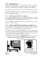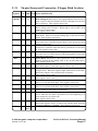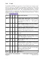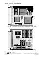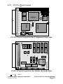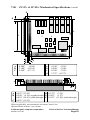
1
The megatel
PC/II+ & PC/II+i
Technical Manual
386SL & 486SL Based Single-Board Computers
megatel computer (1986) corporation
Copyright©
1 July 1999
Release 1.00
Order Number: MA990734-1.00e
megatel computer (1986) corporation
125 Wendell Avenue Weston, Ontario Canada M9N 3K9
©1999 megatel computer corporation
PC/II+ & PC/II+i Technical Manual
Tel: (416) 245-2953 Fax: (416) 245-6505
MA990734-1.00e
Page 1
Limited Warranty
All products (including software) sold are under a LIMITED WARRANTY on
a return-to-factory basis against defects in workmanship and materials for a
period of one year from the date of shipment.
This LIMITED WARRANTY is contingent upon the proper use of the product.
The WARRANTY is void if repairs are necessary due to accident, unusual
physical, electrical, or electro-magnetic stress, misuse, shipping, or causes other
than ordinary use. The WARRANTY will also not apply if the product has been
modified by the BUYER, or if the product has been disassembled by the BUYER.
Disassembly includes the removal of the serial number label on the Product
without prior written permission from megatel.
Any repairs attempted by the customer will void the WARRANTY. Any tips
suggested in the manual or other documentation which involve physical changes
to the board or a reconfiguration of the software will, if attempted, void the
WARRANTY.
Copyright Notice and Trademark acknowledgements. No part of this document
may be copied or reproduced in any form or by any means without prior written
permission from megatel computer (1986) corporation.
Entire contents copyright© megatel computer (1986) corporation, Toronto,
Ontario, Canada, 1993. Printed in Canada.
Disclaimer
megatel makes no representations or warranties with respect to any circuitry
not embodied within a megatel product. megatel specifically disclaims any
implied warranties of merchantability for any particular purpose of any megatel
product.
This manual is for information purposes only. megatel will not be liable for any
direct, indirect, special, incidental, or consequential damages resulting from any
information obtained from this manual.
megatel does not recommend the use of its products in life support applications
wherein in failure or malfunction of the component may directly threaten life or
injury. As part of the terms and conditions of sale, the user of megatel products in
life support applications assumes all risks of such use and indemnifies megatel
against all damages.
megatel assumes no responsibilty for errors which might appear in this document,
and reserves the right to revise this document without notice.
Service Information
Should a megatel product require service, please contact the megatel
Service Department between the hours of 9:00am to 5:00pm EST at TEL. (416)245-2953, or send us a fax at FAX (416)-245-6505.
“megatel” is a registered trademark of megatel computer (1986) corporation
“Intel” is trademarks of Intel Corporation.
“Molex” is a registered trademark of Molex, Inc.
"V-40H" is a trademark of NEC Corporation
“IBM” is a trademark of International Business Machine Corporation & PC, XT® is a registered trademark of IBM
“Apple Macintosh” is a registered trademark of Apple Inc.
“Trantor” is a registered trademark of Trantor Systems, Ltd.
MA990734-1.00e
PC/II+ & PC/II+i Technical Manual
Page 2
©1999 megatel computer corporation
MA990734-1.00e
** WARNING **
MAKE SURE:
The CORRECT VOLTAGE IS APPLIED to the
PC/II+ and PC/II+i
• The voltages required to operate the PC/II+ & PC/II+i are +5V and GND.
• Using a QTB/II*, QTB/104* or QTB/104AT* +5V & GND are connected to the
PC/II+ & PC/II+i via the 96-pin Peripheral Connector and/or the 64-pin ISA
Bus Connector.
• One power connector found on the QTB/II, QTB/104 and QTB/104AT is that of a
4-pin male 3.5" floppy-disk styled power connector (QTB/II uses a straight up
type connector, whereas the QTB/104 and QTB/104AT use the right angle versions).
Molex Part #53133 for the right angle version, with the mating or "housing"
connector Part #5507.
• The total current drawn from the 3.5" floppy-disk styled power connector can
exceed 100mA (3A max).
• The QTB/104 and the QTB/104AT have an additional 8-pin (2x4) right angle
male header power connector for PC/104 power connection compatibility.
4 3 2 1
Male Right Angle
1 +5V
3 GND
3.5" Floppy-styled
2 GND
4 +12V
Power Connector
Male Right Angle
PC/104 compatible
Power Connector
2
8
1
7
1
2
3
4
GND
+5V
KEY
+12V
5
6
7
8
-5V
-12V
GND
+5V
The PC/II+ and PC/II+i is the
FIRST ITEM TURNED ON & the LAST ITEM TURNED OFF
• NEVER turn off the PC/II+ or PC/II+i when there are other peripherals connected
and powered on, such as a printer.
• This is especially important, as the bus and the printer ports are NOT buffered†.
The unbuffered bus and printer port was done to reduce the power requirement of
the board.
• Below is an example of a buffering/filtering circuit which can be used for a single
printer port line.
+5V
R1
D2
R2
From Printer Port Line
To Printer Port
D1
Ground
D1: 1N4148 Signal Diode
D2: +5V TransZorb (Transient Voltage Suppressor)
R1 & R2: 27Ω Resistors
*Note: For more detailed information on the QTB/II, QTB/104 and QTB/104AT,
please see your "QTB Manual".
†Note: The ISA Bus Clock is normally buffered
©1999 megatel computer corporation
MA990734-1.00e
PC/II+ & PC/II+i Technical Manual
Page 3
Table Of Contents
PC/II+ & PC/II+i Technical Manual
Page
Limited Warranty .......................................................................... 2
Disclaimer .................................................................................... 2
Service Information ...................................................................... 2
** WARNING ** ........................................................................ 3
1.00
PC/II+ & PC/II+i Introductions .................................. 7
1.10
1.11
1.12
1.13
1.20
1.30
1.31
1.32
1.40
1.50
1.60
1.61
1.62
1.63
1.70
1.71
1.72
1.80
1.81
1.82
Introduction to the PC/II+ ....................................................... 7
PC/II+ General Specifications ................................................. 7
Introduction to the PC/II+i ...................................................... 8
PC/II+i General Specifications ................................................ 8
General System Notes ............................................................ 9
Power Supply ........................................................................... 9
Reset ......................................................................................... 9
Bus Drive Current .................................................................... 9
Bus Termination Option ........................................................... 9
Main Memory ........................................................................ 10
BIOS/Option ROM/User Memory ......................................... 10
On-board EPROM Enable/Disable Jumper (J5) .................... 10
Interrupts and DMA ............................................................. 11
Interval Timer ....................................................................... 12
Real-Time Clock ................................................................... 13
Real-Time Clock General Information ................................... 13
Real Time Clock Interrupt 1AH ............................................. 14
Real Time Clock Memory Map .............................................. 15
64-pin 8-bit ISA Bus Interface (J2) ..................................... 16
64-pin 8-bit Bus Header Pinout (J2) ....................................... 17
64-pin 8-bit Bus Pinout (J2) ................................................... 18
16-bit Bus Expansion Interface (J3) ................................... 25
16-bit Bus Header Pinout (J3) ................................................ 26
10-pin 16-bit Bus Expansion Pinout (J3) ............................... 26
2.00
96-Pin Peripheral I/O Connector (J1) ........................ 28
2.10
2.11
2.12
2.13
2.14
Video Interface ...................................................................... 29
LCD Control ........................................................................... 29
LCD Driver Files .................................................................... 30
Some Compatible LCD Signal Names ................................... 31
LCD Portion of RTC Memory Map ....................................... 31
continued on next page
PC/II+ & PC/II+i Technical Manual
Page 4
©1999 megatel computer corporation
MA990734-1.00e
Table Of Contents
PC/II+ & PC/II+i Technical Manual
2.15
2.20
2.21
2.30
2.31
2.40
2.41
2.50
2.51
2.52
2.53
2.54
2.60
2.61
2.62
2.63
2.64
2.70
2.71
2.72
Page
96-pin Eurocard Connector: Video Section ............................ 32
Using VGA 65530 Video Controller with VGA Monitor ...... 32
Using VGA 65530 Video Controller with EGA Monitor ....... 32
Using VGA 65530 Video Controller with STN LCD's .......... 32
Chart 1: Common Interfaces (pin assignments) and Settings 33
Parallel Printer Port ............................................................. 34
96-pin Eurocard Connector: Printer Section .......................... 35
Floppy Disk Interface ........................................................... 36
96-pin Eurocard Connector: Floppy Disk Section ................. 37
SCSI Interface ....................................................................... 38
96-pin Eurocard Connector: SCSI Section ............................. 39
Serial Communications Ports .............................................. 40
Com1: Primary Communications Port ................................... 40
Com2: Secondary Communications Port ............................... 40
96-pin Eurocard Connector: Com1 RS-232 Section .............. 41
96-pin Eurocard Connector: Com2 RS-232 Section .............. 42
Auxiliary I/O ......................................................................... 43
96-pin Eurocard Connector: Speaker Section ........................ 43
96-pin Eurocard Connector: Reset Section ............................ 43
96-pin Eurocard Connector: Keyboard Section ..................... 43
Com4 ....................................................................................... 44
Other I/O Pinouts & Descriptions ....................................... 45
96-pin Eurocard Connector: Reserved Pins ........................... 45
96-pin Eurocard Connector: Power Supply Section .............. 45
3.00
ISA High Integration Ethernet Controller ................ 46
3.10
Ethernet 10-pin Header ........................................................... 47
4.00
Flashd ............................................................................. 48
Non-Volatile On-board Solid State Disk ................................ 48
5.00
I/O Addresses ............................................................... 49
Standard I/O Map .................................................................... 49
6.00
Parts Lists & Parts Layouts ........................................ 50
6.10
6.11
6.20
6.21
PC/II+ Parts List ..................................................................... 50
PC/II+ Parts Layout ................................................................ 51
PC/II+i Parts List .................................................................... 52
PC/II+i Parts Layout ............................................................... 53
7.00
8.00
9.00
PC/II+ & PC/II+i Mechanical Specifications ............ 54
References ..................................................................... 56
megatel Service Procedure ......................................... 57
megatel SERVICE FORM ................................................. 58
©1999 megatel computer corporation
MA990734-1.00e
PC/II+ & PC/II+i Technical Manual
Page 5
Notes
PC/II+ & PC/II+i Technical Manual
Page 6
©1999 megatel computer corporation
MA990734-1.00e
1.00 PC/II+ & PC/II+i Introductions
1.10
Introduction to the PC/II+
The PC/II+ is a surface mounted single-board computer based on the
Intel386™SL microprocessor and the Intel® 82360SL I/O Subsystem. It
features up to 10MBytes of on-board user DRAM; up to 256KByte BIOS
ROM; on-board 2MByte Solid State Disk; a graphics display controller
supporting color LCD panels and analog VGA/SVGA monitors; a floppy
disk controller; two full IBM compatible RS-232 serial communication
ports; a partial RS-232 Serial port (used via BIOS calls); an Ethernet Local
Area Network (802.3 compliant AUI & TPE [10BASE-T] signal interfaces);
one parallel printer port; a serial keyboard port; a real time clock-calandar
with battery back-up; and an 8-bit ISA or 16-bit Bus interface.
1.11
PC/II+ General Specifications
CPU & MEMORY:
•Intel386™SL Microprocessor
•25MHz CPU clock frequency
•Static Intel386 CPU core
•AT compatible BIOS and Architecture
•Up to 256KByte BIOS ROM
•Up to 10MByte User DRAM
INPUT/OUTPUT:
•On-board 8-bit ISA or 16-bit Bus Expansion
•Standard IBM XT Keyboard port
•IBM compatible bi-directional Parallel Port
•2 IBM compatible RS-232 Serial ports
•1 RS-232 Serial subsystem
(Txdata, Rxdata, & BIOS Interface)
•AT Real-time clock (& Battery Back-up)
VGA VIDEO CONTROLLER:
•Supports Analog VGA/SVGA Monitors
FLOPPY DISK CONTROLLER:
and LCD, EL & Gas Plasma displays
•CMOS Floppy Disk Controller
•Up to 512KB Video DRAM
•Can drive 360KByte, 720KByte, 1.2MByte,
•Enhanced backward compatibility
or 1.44MByte capacity drives
with EGA™, CGA™, Hercules™
•Can support up to two drives
& MDA™ standards
•Will boot standard versions of PC,
•Supports Color flat panels (ie. TFT & STN) MS DOS®, and DR DOS
•Supports panels from popular
manufacturers such as Sharp,
NETWORK:
Densitron and Seiko/Epson
•On-board Ethernet LAN
•VGA Register Set Compatible
(Local Area Network)
•802.3 compliant AUI and TPE (10BASE-T)
SCSI CONTROLLER:
serial interfaces
•ASPI compatible SCSI controller
•Automatic switching between AUI and
•Standard IBM PC AT Hard Disk BIOS
TPE ports
support via SCSI port
•64KBytes local DRAM
•Complete interface for SCSI
•16-bit I/O accesses local DRAM with
compatible hard drives
zero added wait states
•Multi-media software supports
CD ROMs, audio devices and optical
MISCELLANEOUS:
storage
•Only 100mmx100mm (4"x4")
•Requires only +5V operation
SOLID STATE DISK:
•Power consumption less than 5 Watts
•On-board 2MByte solid state disk (typical)
•megatel drivers for reading & writing
©1999 megatel computer corporation
MA990734-1.00e
PC/II+ & PC/II+i Technical Manual
Page 7
1.12
Introduction to the PC/II+i
The PC/II+i is a surface mounted single-board computer based on the
Intel486SL™ microprocessor and the Intel® 82360SL I/O Subsystem. It
features up to 16MBytes of on-board user DRAM (protected mode); up to
256KByte BIOS in Flash™ EPROM; on-board 2MByte Solid State Disk;
a graphics display controller supporting color LCD panels and analog VGA/
SVGA monitors; a floppy disk controller; two full IBM compatible RS232 serial communication ports; a partial RS-232 Serial port (used via BIOS
calls); an Ethernet Local Area Network (802.3 compliant AUI & TPE
[10BASE-T] signal interfaces); one parallel printer port; a serial keyboard
port; a real time clock-calandar with battery back-up; and an 8-bit ISA or
16-bit Bus interface.
1.13
PC/II+i General Specifications
CPU & MEMORY:
•Intel486™SL Microprocessor
•25MHz or 33MHz CPU clock frequency
•Built-in 8K Cache; floating point unit
•Full 32-bit DRAM Data Bus
•486DX compatibility & performance
•AT compatible BIOS and Architecture
•Up to 256KByte BIOS in Flash™ EPROM
•4MByte or 16MByte User DRAM
•PC/104 Bus Compatible option with Adapter
•ISA Bus Compatible option with Adapter
INPUT/OUTPUT:
•On-board 8-bit ISA or 16-bit Bus Expansion
•Standard IBM PC Keyboard port
•8-bit general purpose Parallel Port
•2 IBM compatible RS-232C Serial ports
•1 BIOS compatible RS-232C serial port
(Txdata, Rxdata, to a BIOS interface)
•Independent software selectable BAUD rates
•Voltage converter for serial +/- voltages
•AT Real-time clock with Battery Back-up
•M-Systems Flash File System
SOLID STATE DISK:
FLOPPY DISK CONTROLLER:
•On-board 2MByte solid state disk (typical) •CMOS Floppy Disk Controller
•Can drive 360KByte, 720KByte, 1.2MByte,
•megatel drivers for reading & writing
or 1.44MByte capacity drives
VGA VIDEO CONTROLLER:
•Can support up to two drives
•Supports Analog VGA/SVGA Monitors
•Will boot standard versions of PC,
and LCD, EL & Gas Plasma displays
MS DOS®, and DR DOS
•Up to 512KB Video DRAM
•Enhanced backward compatibility
NETWORK:
with EGA™, CGA™, Hercules™
•On-board Ethernet LAN (Local Area Network)
& MDA™ standards
•802.3 compliant AUI and TPE (10BASE-T)
•Supports Color flat panels (ie. TFT & STN) serial interfaces
•Supports panels from popular
•Automatic switching between AUI and
manufacturers such as Sharp & Seiko
TPE ports
•64KBytes local DRAM
SCSI CONTROLLER:
•16-bit I/O accesses local DRAM with
•5380 compatible SCSI controller
zero added wait states
•ASPI compatible software drivers included
•Standard IBM PC AT Hard Disk BIOS
MISCELLANEOUS:
support via SCSI port (INT13h)
•Only 100mmx100mm (4"x4")
•Complete interface for SCSI
•Requires only +5V operation
compatible hard drives
•Power consumption of 6 Watts (typical for
•Multi-media software supports CD ROMs, 33MHz board with 4MBytes DRAM)
audio devices and optical storage
•MTBF: Not less than 200,000 hours
PC/II+ & PC/II+i Technical Manual
Page 8
©1999 megatel computer corporation
MA990734-1.00e
1.20 General System Notes
Power Supply
The PC/II+ & PC/II+i use +5V ±5%.
The voltage Rise time should be from +2V to +5V within 10ms.
Reset
The /Reset line found at J1 pin 31A (96-pin eurocard connector)
should be driven by an open-collector or mechanical switch.
Bus Drive Current
All Bus signals except for the /BS16 signal can be driven with
devices capable of providing 4mA sink current.
/BS16 signal can be driven with devices capable of providing
10mA sink current.
Note: The /BS16 signal is equivalent to the /IOCS16 and
/MEMCS16 signal.
Bus Termination Option
AC Bus termination provides termination close to the
characteristic impedance of the signal lines without exceeding
the DC output current capabilities of the drivers. This increases
data integrity and system reliability. A resistor-capacitor
network of 40-60 ohms in series with 30-70pF can be connected
between each bus signal and ground.
©1999 megatel computer corporation
MA990734-1.00e
PC/II+ & PC/II+i Technical Manual
Page 9
1.30 Main Memory
The standard PC/II+ utilizes a total of 2MByte, 4MByte, 8MByte or
10MBytes of user DRAM. In the 4MByte system, page-interleaving is
utilized. The PC/II+i utilizes 4MBytes or 16MBytes of user DRAM.
The average/effective wait states in H.S. Fast Page Mode is 0.2 wait states.
The BIOS automatically checks the memory at Power-On to determine
the amount of RAM available. No straps or jumpers are needed to specify
the size of the Main Memory.
1.31
BIOS/Option ROM/User Memory
The standard ROM installed on the PC/II+ or PC/II+i is a 2Mbit
(256KByte) E28F020 Flash EPROM which contains the BIOS (including
the VGA BIOS and SCSI Option ROM) for the system.
There is 128kBytes of user Option Module space/Bus space located from
address C0000h to DFFFFh.
1.32
On-board EPROM Enable/Disable Jumper (J5)
Since the PC/II+ or PC/II+i on-board Flash BIOS EPROM is soldered
onto the board, a 2-pin jumper has been installed to allow an external
EPROM, which contains our BIOS, to be used via the bus.
To disable the on-board Flash BIOS EPROM remove the shorting plug,
from the 2-pin jumper, that is located at the edge of the board that sides the
196-pin 386SL and the 44-pin 82595 Ethernet controller. By removing the
shorting plug, the on-board BIOS EPROM is disabled.
This jumper is used strictly by megatel and must be installed
in order for the PC/II+ or PC/II+i to function properly.
Do not remove.
386SL
J5
1
1
82595
PC/II+ & PC/II+i Technical Manual
Page 10
To Use On-board
BIOS EPROM:
Leave shorting plug on.
©1999 megatel computer corporation
MA990734-1.00e
1.40 Interrupts and DMA
The PC/II+ & PC/II+i utilizes the Intel® 82360SL to provide 8259
compatible interrupt request lines and 8237 compatible DMA channels.
Within the 82360SL, two interrupt controllers are used to provide interrupt
request lines and two DMA controllers are used to provide DMA request
lines. One interrupt line (IRQ2) is used to cascade the two interrupt
controllers together leaving a total of 14 interrupt request lines. One DMA
channel (DRQ4) is used to cascade the two DMA controllers together
leaving a total of 7 DMA channels. The interrupt request lines and DMA
channels are shown in the tables below.
Interrupt (IRQ)
(Controller 1) (Controller 2)
0
1
2
9
3
4
5
6
7
8
10
11
12
13
14
15
DMA (DRQ)
(Controller 1) (Controller 2)
0
1
2
3
4
5
6, 7
Description
Available
On Bus
Timer
Keyboard
VGA Controller
(NOTE: In ISA systems, IRQ2=IRQ9)
Serial Port (Com2)
Serial Port (Com1)
Unused
Floppy Disk Controller
Printer
RTC Timer/Alarm
Unused
Ethernet
Mouse
Reserved (Numeric Co-Processor)
Reserved (IDE Hard Drive)
SCSI Controller
Description
SCSI Controller
Unused
Floppy Disk
Unused
Cascades to Controller 1 via
DMA Channel 4
Reserved
Unused (DRQ6 tied to DRQ7;
/DACK7 tied to /MASTER)
Yes
Yes
Yes
Yes
Yes
Yes
Yes
Yes*
Available
On Bus
Yes
Yes
Yes
Yes*
*Note: Inputs Interrupt 14 & DRQ6 & DRQ7 are hardwired together as DRQ16.
Outputs /DACK6 & /DACK7 are logically ANDED to generate /DACK16.
Overall Note: Since devices tied to Interrupt lines normally Tri-State their outputs,
Interrupts may be shared if the interrupt handler is written to
determine which device actually generated an interrupt.
©1999 megatel computer corporation
MA990734-1.00e
PC/II+ & PC/II+i Technical Manual
Page 11
1.50 Interval Timer
The PC/II+ & PC/II+i utilize the Intel® 82360SL to provide 8254
compatible Programmable Timer Counters.
Timer 0, Timer 1 & Timer 2 are clocked by a 1.193MHz clock, resulting in
a minimum timing resolution of 838ns. The Gate inputs for Timer 0 and
Timer 1 are tied high. The Gate inputs for Timer 2 are controlled by the
Timer 2 Gate Bit, which is Bit 0 of Port 061h.
The output from Timer 0 is connected to interrupt input IRQ0 on the
Interrupt Controller. This timer is used by the operating system for its
internal real-time clock.
The output from Timer 1 is used to generate a CPU Hold Request when it
is time for a refresh cycle.
Timer 2 is used to generate signals for the Speaker output. The Timer 2
output is gated with the SPEAKER DATA bit (bit 1 of Port 061h) to drive
the SPKR output. The combination of the Timer 2 Gate control bit and
the SPEAKER Data bit allow complex waveforms to be generated on
the Speaker output. The state of the TIMER 2 output can be read at Port
061h bit 5.
The Speaker output, SPKR, is pin A9 of the 96-pin eurocard connector
(J1). It is intended to drive a piezo-electric audio transducer
connected between the SPKR pin and ground.
PC/II+ & PC/II+i Technical Manual
Page 12
©1999 megatel computer corporation
MA990734-1.00e
1.60 Real-Time Clock
1.61
Real-Time Clock General Information
The Real-time Clock (RTC) on the PC/II+ & PC/II+i is part of the Intel®
82360SL. The RTC section also uses a 32.768 kHz crystal and a 3.0V
Lithium battery. The battery is soldered onto the circuit board.
Features of the clock chip include:
• 128 Bytes battery backed up CMOS RAM
• Low standby current (5µA @ 3.0V)
• Four Year Calendar
• 24 or 12 Hour Format
• Automatic word addressing incrementing
• Programmable alarm, timer, and interrupt function
The clock comes set at proper date and time from the factory for North
American EST. The software for the clock is included as part of the BIOS
with boards containing the Real-Time-Clock option. Standard features of
the RTC option include both leap year and year changeover.
The DOS clock is updated automatically by the RTC upon Boot Up. Should
you change the time or date in DOS, the PC/II+ & PC/II+i will conversely
update the RTC chip. The PC/II+ & PC/II+i uses standard DOS instructions
to change the time and the date. If you are using standard DOS where the
time and date is displayed upon boot up, you may change the time and date
at this point. While in DOS, the time and date can also be changed by
typing TIME, then entering the desired time and typing DATE, then entering
the desired date.
The 128 Bytes of battery backed CMOS RAM is also used to store
information pertaining to the CMOS RAM SETUP & LCD Driver file
values.
The CMOS RAM SETUP includes such information as the time and date;
the amount of useable memory available; video mode (monitor type); floppy
disk drive type and whether there are one or two drives connected. (For
more information regarding the CMOS RAM SETUP, please read the
"Options and Defaults in the PC/II+ Series SBC CMOS RAM SETUP"
section in the "PC/+v & PC/II+ Series Products User's Manual")
When using an LCD panel, EL or Plasma display, a driver file must be
loaded into the 65530 Video controller registers. The LCD driver file values
are stored in the CMOS RAM of the Real-Time Clock and loaded into the
proper 65530 registers upon boot up (For more information regarding LCD
driver files, please read the "65530 LCD Manual", formerly entitled the
"PC/II+ LCD Manual").
continued on next page
©1999 megatel computer corporation
MA990734-1.00e
PC/II+ & PC/II+i Technical Manual
Page 13
The real time clock is addressed at I/O Address 0070h-0071h and drives
IRQ8.
The 3.0V Lithium battery is rated for 190mAh to 200mAh (typical) in an
operation temperature range of -20˚C to +70˚C. The storage temperature
range is -40˚C to +60˚C and the Self discharge is less than 1% per year at
25˚C. It is intended for use with the Real-Time Clock only.
1.62
Real Time Clock Interrupt 1AH
The PC/II+ & PC/II+i support the Interrupt 1AH AT compatible clock
functions.
CLKGET & CLKPUT are two other real time clock functions that are
implemented on the PC/II+ & PC/II+i, accessible through INT1AH.
Function Prior To INT1AH Upon Return from INT1AH
CLKGET AH=FEH
AL=Value in real time clock register
DL=register*
DH=1DH
NOTE: *register=specify real time clock register
CLKPUT AH=FFH
No values returned
DL=register*
DH=1CH
AL=value**
NOTE: *register=specify real time clock register
**value =specify value to go into register
PC/II+ & PC/II+i Technical Manual
Page 14
©1999 megatel computer corporation
MA990734-1.00e
1.63
Real Time Clock Memory Map
Register Address
Function
Decimal Hexadecimal
000
001
002
003
004
005
006
007
008
009
010-013
014
015
016
017
018
019
020
021
022
023
024
025
026
027
028-045
046
047
048
049
050
051
053-064
065
066-074
075
076
077
078-079
080-127
Note:
00h
01h
02h
03h
04h
05h
06h
07h
08h
09h
0Ah-0Dh
0Eh
0Fh
10h
11h
12h
13h
14h
15h
16h
17h
18h
19h
1Ah
1Bh
1Ch-2Dh
2Eh
2Fh
30h
31h
32h
33h
35h-40h
41h
42h-4Ah
4Bh
4Ch
4Dh
4Eh-4Fh
50h-7Fh
Control/Status
100ths of a Second
Seconds
Minutes
Hours
Year/Century
Month/Day
Timer
Reserved for Alarm Control
Reserved for Alarm Registers or Ram
Status Registers A, B, C, D
Diagnostic Status Byte
Shutdown Status Byte
Floppy Drive Type Byte
Reserved
Fixed Drive Type Byte
Reserved
Equipment Byte
Base Memory Size (Low Byte)
Base Memory Size (High Byte)
Expanded Memory Size (Low Byte)
Expanded Memory Size (High Byte)
Drive C - Fixed Drive Type (Extended Byte)
Drive D - Fixed Drive Type (Extended Byte)
Reserved
Reserved
Checksum (Low Byte) for registers 10h-2Dh
Checksum (High Byte) for registers 10h-2Dh
Expanded Memory Size (Low Byte)
Expanded Memory Size (High Byte)
Date Century Byte
Information Flags
Reserved
Equipment Byte (Extended)
Reserved
Reserved - LCD Signature
Reserved - LCD Type Byte
Reserved
Reserved
Reserved
When using the Direct Edit of the CMOS RAM SETUP, only registers 10h
to 7Fh are accessible.
©1999 megatel computer corporation
MA990734-1.00e
PC/II+ & PC/II+i Technical Manual
Page 15
1.70 64-pin 8-bit ISA Bus Interface (J2)
The PC/II+ & PC/II+i Bus interface provides a quick route for adding
a variety of standard I/O functions while keeping the complexity and
physical size of the system to a minimum. OEM users who are designing
their own special purpose I/O functions, may find it convenient to use the
PC/II+ or PC/II+i Bus interface.
Note: I/O cycles, with /BS16 selected as a 16-bit bus, must be qualified
with /IOR and /IOW OR with the top bits (A15 to A19) addressing
00000hex. (see "16-bit Bus Expansion" chapter)
The 8-bit ISA Bus connector (J2) found on the standard PC/II+ & PC/II+i
is that of a 64-pin dual row header (2x32, on 0.100" [2.54mm] spacing).
The last 62 pins of J2 (pins A1 to A31 and B1 to B31) correspond to the PC
Bus interface.
The 8-bit ISA Bus connector found on the custom PC/II+ & PC/II+i is
that of a 62-pin male edge connector.
* WARNING *
The following signals used on the PC/II+ & PC/II+i 8-bit Bus
are NOT Power pins.
PC/II+ & PC/II+i
J2 Pin #
B5
B7
B9
PC/II+ & PC/II+i 8-bit
Bus Name
IRQ10
/DACK16
IRQ14 (DRQ16)
Old XT or AT
Signal Name
-5V
-12V
+12V
Bus Termination Option
AC Bus termination provides termination close to the characteristic
impedance of the signal line without exceeding the DC output current
capabilities of the drivers. This increases data integrity and system
reliability. A resistor-capacitor network of 40-60 ohms in series with 3070pF can be connected between each bus signal and ground.
Bus Drive Current
All Bus signals except for the /BS16 signal can be driven with devices
capable of providing 4mA sink current.
The /BS16 signal can be driven with devices capable of providing 10mA
sink current. Note: The /BS16 signal is equivalent to the /IOCS16 and the
/MEMCS16 signal.
For Bus timing, please refer to the "References" section of this manual.
PC/II+ & PC/II+i Technical Manual
Page 16
©1999 megatel computer corporation
MA990734-1.00e
1.71
64-pin 8-bit Bus Header Pinout (J2)
J2
Pin A0
Pin B0
* WARNING *
Some of these signals (*) USED TO BE power pins
DO NOT CONNECT POWER TO THESE PINS!!!
PC Bus
Name
PC/II+(i)
J2
PC/II+(i)
J2
PC Bus
Name
GND
/IOCHK
D7
D6
D5
D4
D3
D2
D1
D0
IORDY
AEN
A19
A18
A17
A16
A15
A14
A13
A12
A11
A10
A9
A8
A7
A6
A5
A4
A3
A2
A1
A0
A0
A1
A2
A3
A4
A5
A6
A7
A8
A9
A10
A11
A12
A13
A14
A15
A16
A17
A18
A19
A20
A21
A22
A23
A24
A25
A26
A27
A28
A29
A30
A31
B0
B1
B2
B3
B4
B5
B6
B7
B8
B9
B10
B11
B12
B13
B14
B15
B16
B17
B18
B19
B20
B21
B22
B23
B24
B25
B26
B27
B28
B29
B30
B31
+5V
GND
RESET
+5V
IRQ2
IRQ10*
DRQ2
/DACK16*
/0WS
IRQ14 (DRQ16)*
GND
/MEMW
/MEMR
/IOW
/IOR
/DACK3
DRQ3
/DACK1
DRQ1
REFRESH
CLK
IRQ7
IRQ6
IRQ5
IRQ4
IRQ3
/DACK2
TC
ALE
+5V
OSC
GND
©1999 megatel computer corporation
MA990734-1.00e
PC/II+ & PC/II+i Technical Manual
Page 17
1.72
64-pin 8-bit Bus Pinout (J2)
Symbol
Pin No. Type Name and Function
A0-A19 A31-A12
O
CPU Address lines: These lines provide the
memory and I/O address for the entire bus
cycle. These lines are active high.
D0-D7
A9-A2
I/O Bi-directional Data Bus: Data is input on
these lines during memory, I/O, and interrupt
acknowledge read cycles. Data is output on
these lines during memory and I/O write
cycles.
These lines are active high.
+AEN
A11
O
Address Enable: AEN is used to indicate
that DMA transfers are taking place. This
line is active high. When this line is active,
the DMA controller has control of the
address bus, the data-bus Read command
lines (memory and I/O) and the data-bus
Write command lines (memory and I/O).
+IORDY
A10
I
I/O Channel Ready: I/O Channel Ready is
the acknowledgement from the addressed
memory or I/O device that it will complete
the data transfer. This line is active high. A
low input on this line will insert wait-states
into the processor's bus cycle to lengthen I/
O or memory cycles so that it may complete
its read or write transfer. This line should
not be held low for no more than 2.5
microseconds.
/IOCHK
A1
I
I/O Channel Check: -I/OCHK provides the
CPU with parity error information regarding
the memory or devices using the I/O channel.
This signal is active low. When this signal is
active, an interrupt is generated to the CPU.
+OSC
B30
O
Oscillator: The OSC is a constant speed
14.31818MHz clock. This signal is not
synchronous with the system clock and has
a duty cycle of 50%.
continued on next page
PC/II+ & PC/II+i Technical Manual
Page 18
©1999 megatel computer corporation
MA990734-1.00e
1.72
64-pin 8-bit Bus Pinout (J2) (continued)
Symbol
Pin No. Type Name and Function
+ALE
B28
O
Address Latch Enable: This signal is used
to latch valid addresses and memory
decodes from the microprocessor. When
used with AEN, this signal is available to
the I/O channel to indicate valid
microprocessor or DMA addresses. ALE is
an active high signal and microprocessor
addresses are latched on the falling edge
(high to low) of the ALE signal.
TC
B27
O
Terminal Count: A pulse is put on this
line to indicate that the current DMA
transfer has reached the terminal count.
This signal is active high.
/REFRESH
B19
O
Refresh: This signal is used to refresh
dynamic ram and can be driven by a
microprocessor on the I/O channel This
signal is active low. In the traditional
PC/XT architecture this channel is also
known as -DACK0.
/DACK1
/DACK3
B17
B15
O
O
DMA Acknowledge 1 & 3 (Spare):
DACK1 & DACK3 are used to
acknowledge DMA requests which notifies
the individual peripheral it has been granted
a DMA cycle. These lines are active low.
/DACK2
B26
O
DMA Acknowledge 2 (Floppy): DACK2
is used to acknowledge DMA requests
which notifies the individual peripheral it
has been granted a DMA cycle.
This line is active low.
+DRQ1
+DRQ3
B18
B16
I
I
DMA Request Line 1 and 3 (Spare):
These lines are individual asynchronous
channel request lines input used by
peripheral circuits to obtain DMA service.
In the traditional XT architecture DRQ1 is
unused and DRQ3 is used for a fixed disk
controller.
These lines are active high.
continued on next page
©1999 megatel computer corporation
MA990734-1.00e
PC/II+ & PC/II+i Technical Manual
Page 19
1.72
64-pin 8-bit Bus Pinout (J2) (continued)
Symbol Pin No. Type
Name and Function
+DRQ2
B6
I
DMA Request Line 2 (Floppy): DRQ2 is an
individual asynchronous channel request
input used by the floppy disk controller to
obtain DMA service. This line is active high.
+IRQ2
(IRQ9)
B4
I
Interrupt Request 2 (EGA/VGA):
IRQ2 is an asynchronous input used to request
interrupt service. An interrupt request is
executed by raising IRQ2 (low to high) and
holding it high until it is acknowledged (edge
triggered mode), or holding IRQ2 at a high
level until it is acknowledged (level triggered
mode). This line is active high. In the PC/II+
& PC/II+i architecture, this line is used by
the video controller. In the traditional XT/
AT architecture this channel is used by LPT2
and some network cards.
+IRQ3
B25
I
Interrupt Request 3 (Com2): IRQ3 is an
asynchronous input used to request interrupt
service. An interrupt request is executed by
raising IRQ3 (low to high) and holding it high
until it is acknowledged (edge triggered
mode), or holding IRQ3 at a high level until it
is acknowledged (level trigger mode). This
line is active high. In the PC/II+, PC/II+i and
traditional XT/AT architecture, this channel is
used by the Com2 port and some network
cards.
+IRQ4
B24
I
Interrupt Request 4 (Com1): IRQ4 is
asynchronous input used to request interrupt
service. An interrupt request is executed by
raising IRQ4 (low to high) and holding it high
until it is acknowledged (edge triggered
mode), or holding IRQ4 at a high level until it
is acknowledged (level triggered mode). This
line is active high. In the PC/II+, PC/II+i and
traditional XT/AT architecture, this channel is
used by the Com1 port and some network
cards.
continued on next page
PC/II+ & PC/II+i Technical Manual
Page 20
©1999 megatel computer corporation
MA990734-1.00e
1.72
64-pin 8-bit Bus Pinout (J2) (continued)
Symbol Pin No. Type Name and Function
+IRQ5
B23
I
Interrupt Request 5 (Spare): IRQ5 is an
asynchronous input used to request interrupt
service. An interrupt request is executed by
raising IRQ5 (low to high) and holding it high
until it is acknowledged (edge triggered
mode), or holding IRQ5 at a high level until
it is acknowledged (level triggered mode). This
line is active high. In the PC/II+, PC/II+i
and traditional XT/AT architecture, this
channel is used by the fixed disk controller.
+IRQ6
B22
I
Interrupt Request 6 (Floppy Disk): IRQ6 is
an asynchronous input used to request interrupt
service. An interrupt request is executed by
raising IRQ6 (low to high) and holding it high
until it is acknowledged (edge triggered
mode), or holding IRQ6 at a high level until it
is acknowledged (level triggered mode). This
line is active high. In the PC/II+, PC/II+i and
traditional XT/AT architecture, this channel is
used by the floppy disk controller.
+IRQ7
B21
I
Interrupt Request 7 (Printer Port): IRQ7 is
an asynchronous input used to request interrupt
service. An interrupt request is executed by
raising IRQ7 (low to high) and holding it high
until it is acknowledged (edge triggered
mode), or holding IRQ7 at a high level until it
is acknowledged (level triggered mode). This
line is active high. In the PC/II+, PC/II+i and
traditional XT/AT architecture, this channel is
used by the parallel printer port (LPT1).
CLK
B20
O
Bus Clock: Clock is the processor clock. This
clock is a square wave with a frequency of
12.5MHz or 16MHz (PC/II+i only). Note:
Special orders will allow boards to be shipped
with a hardware strapped clock of 1/2 the
System Clock.
/IOR
B14
O
I/O Read: IOR instructs an I/O device to place
data onto the I/O channel.
This signal is active low.
continued on next page
©1999 megatel computer corporation
MA990734-1.00e
PC/II+ & PC/II+i Technical Manual
Page 21
1.72 64-pin 8-bit Bus Pinout (J2) (continued)
Symbol
Pin No. Type Name and Function
/IOW
B13
O
I/O Write: IOW instructs an I/O device to
read data off of the I/O channel. This signal
is active low.
/MEMR
B12
O
Memory Read: MEMR instructs the
memory to place data onto the I/O channel.
The signal is active low.
/MEMW
B11
O
Memory Write: MEMW instructs the
memory to read data off of the I/O channel.
This signal is active low.
RESET
B2
O
Reset Drive: Reset Drv indicates that a
reset conditon is in progress. This signal
is active high and is synchronized to the
falling edge of CLK.
B0, B3
B29
I
VCC: Externally supplied +5V
+5V
GND
A0, B1 I/O
B10, B31
GND: Power return of power supply
WARNING
The following pin assignments are
NO LONGER USED AS POWER PINS
DO NOT APPLY POWER TO THESE PINS!!!!
IRQ14
B9
I
B9
I
(No longer
+12V)
/DRQ16
Interrupt Request 14 (Spare): IRQ14 is
an asynchronous input used to request
interrupt service. An interrupt request is
executed by raising IRQ14 (low to high)
and holding it high until it is acknowledged
(edge triggered mode), or holding IRQ14
at a high level until it is acknowledged
(level triggered mode). This line is active
high. In the traditional AT architecture,
this channel is used by the IDE fixed disk.
DMA Request Line 16: IRQ14, DRQ6
& DRQ7 are hardwired together as
DRQ16.
continued on next page
PC/II+ & PC/II+i Technical Manual
Page 22
©1999 megatel computer corporation
MA990734-1.00e
1.72
64-pin 8-bit Bus Pinout (J2) (continued)
WARNING
Some of the following pin assignments are
NO LONGER USED AS POWER PINS
DO NOT APPLY POWER TO THESE PINS!!!!
Symbol
/0WS
Pin No. Type Name and Function
B8
O
Zero Wait States: In the traditional XT
architecture, this pin was used for /Card
Select. In the PC/II+, PC/II+i and
traditional AT architecture, this pin is used
for 0WS (zero wait states).
This pin is active low.
B7
O
DMA Acknowledge 16 (Spare): DACK16
is used to acknowledge DMA requests
which notifies the individual peripheral it
has been granted a DMA cycle. These lines
are active low. In the traditional XT and
AT this pin was used for -12V or unused.
/DACK6 & /DACK7 are logically ANDED
together to generate /DACK16.
B5
I
Interrupt Request 10 (Spare): IRQ10 is
an asynchronous input used to request
interrupt service. An interrupt request is
executed by raising IRQ10 (low to high)
and holding it high until it is acknowledged
(edge triggered mode), or holding IRQ10
at a high level until it is acknowledged
(level triggered mode). This line is active
high. In the traditional XT architecture,
this channel is used for -5V. In the
traditional AT architecture, this channel is
unused.
(No Longer
/Card Select)
/DACK16
(No Longer
-12V)
IRQ10
(No Longer
-5V)
©1999 megatel computer corporation
MA990734-1.00e
PC/II+ & PC/II+i Technical Manual
Page 23
Notes
PC/II+ & PC/II+i Technical Manual
Page 24
©1999 megatel computer corporation
MA990734-1.00e
1.80 16-bit Bus Expansion Interface (J3)
The PC/II+ & PC/II+i also provide an expansion to a 16-bit Data Bus
interface, in the form of the additional 10-pin single row header strip (J3)
(1x10, on 0.100" [2.54mm] spacing).
Note: I/O cycles, with /BS16 selected as a 16-bit bus, must be qualified
with /IOR and /IOW OR with the top bits (A15 to A19) addressing
00000hex.
Bus Termination Option
AC Bus termination provides termination close to the characteristic
impedance of the signal line without exceeding the DC output current
capabilities of the drivers. This increases data integrity and system
reliability. A resistor-capacitor network of 40-60 ohms in series with 3070pF can be connected between each bus signal and ground.
Bus Drive Current
All Bus signals except for the /BS16 signal can be driven with devices
capable of providing 4mA sink current.
The /BS16 signal can be driven with devices capable of providing 10mA
sink current.
Note: The /BS16 signal is equivalent to the /IOCS16 and /MEMCS16 signal.
For Bus timing, please refer to the "References" section of this manual.
©1999 megatel computer corporation
MA990734-1.00e
PC/II+ & PC/II+i Technical Manual
Page 25
1.81
16-bit Bus Header Pinout (J3)
J3
PC Bus Name
/BS16
D15
D14
D13
D12
D11
D10
D9
D8
/SBHE
1.82
PC/II+ & PC/II+i
(J3) Pin No.
1
2
3
4
5
6
7
8
9
10
10-pin 16-bit Bus Expansion Pinout (J3)
Symbol
/BS16
Pin 1
Pin No. Type Name and Function
1
I
Bus Select 16: This signal indicates that
an ISA bus peripheral wishes to execute a
16-bit I/O cycle. This signal has an active
pull-up, so when not driven, the default
I/O bus cycle is 8 bits.
This signal is active low.
D15 to D8 2, 3, 4, 5, I/O
6, 7, 8, 9
Bi-directional Data Bus: Data is
input on these lines during memory, I/O,
and interrupt acknowledge read cycles.
Data is output on these lines during
memory and I/O write cycles.
These lines are active high.
/SHBE
System Byte High Enable: This signal
indicates that data is being transferred on
the upper byte of the 16-bit data bus (D8
to D15).
This signal is active low.
10
O
PC/II+ & PC/II+i Technical Manual
Page 26
©1999 megatel computer corporation
MA990734-1.00e
Notes
©1999 megatel computer corporation
MA990734-1.00e
PC/II+ & PC/II+i Technical Manual
Page 27
2.00 96-Pin Peripheral I/O Connector (J1)
32
1
Right Angle 96-pin DIN
(Eurocard Connector)
C
B
A
C
B
A
32
1
Straight Up 96-pin Header
PIN
1
2
3
4
5
6
7
8
9
10
11
12
13
14
15
16
17
18
19
20
21
22
23
24
25
26
27
28
29
30
31
32
A
VID-P3 (SB or VID)
VID-P5 (SR)
VID-P8*
VID-SCK
VID-M†
VID-P10 (ANBLUE)
VID-P11 (ANRED)
RESERVED
SPEAKER
PRN-SLCT
PRN-PE
PRN-BUSY
PRN-AKN
PRN-D7
PRN-D6
PRN-D5
PRN-D4
PRN-D3
PRN-D2
PRN-D1
PRN-D0
PRN-STRB
SCSI-D0
SCSI-D1
SCSI-D2
SCSI-D3
SCSI-D4
SCSI-D5
SCSI-D6
SCSI-D7
SCSI-DP
/RESET
ROWS
B
VCC
VID-P0 (BLUE)
VID-P1 (GREEN)
VID-P2 (RED)
VID-GND
VID-P6 (LD0)
COM2-RI
COM2-DTR
COM2-CTS
COM2-TXD
COM2-RTS
COM2-RXD
COM2-DSR
COM2-DCD
COM4-RX
COM4-TX
KBD-DATA
KBD-CLK
PRN-SELECTIN
PRN-INIT
PRN-ERR
PRN-AUTO
SCSI-ATN
SCSI-BSY
SCSI-AKN
SCSI-RST
SCSI-MSG
SCSI-SEL
SCSI-C/D
SCSI-REQ
SCSI-I/O
VCC
Component (Top) View
C
GND
VID-FRM (VSYNC)
VID-LC (HSYNC)
VID-P9 (ANGREEN)
VID-P4 (INT or SG)
VID-P7 (LD1)
COM1-RI
COM1-DTR
COM1-CTS
COM1-TXD
COM1-RTS
COM1-RXD
COM1-DSR
COM1-DCD
FDD-DCHG
FDD-HS
FDD-RDD
FDD-WP
FDD-TRK0
FDD-WE
FDD-WD
FDD-STP
FDD-DIRC
FDD-MD2
FDD-DS1
FDD-DS2
FDD-MD1
FDD-IDX
FDD-GND
RESERVED
FDD-RPM
GND
*Note: J1A pin 3 can be connected to P8 instead of being connected to /ENAVEE.
†Note: J1A pin 5 can be connected to /BLANK instead of being connected to the
M signal.
PC/II+ & PC/II+i Technical Manual
Page 28
©1999 megatel computer corporation
MA990734-1.00e
2.10
Video Interface
The Video Interface on the PC/II+ & PC/II+i utilizes the Chips® 65530 Video
Controller. This interface is compatible with the IBM-PS/2 Video Graphics Array
(VGA).
The VGA Controller I/O Address is 03B0h-03DFh and utilizes IRQ2 (IRQ9).
The Video Interface includes a separate 512KByte* of Read/Write memory called
the "Display Buffer or Character generator video RAM", in which the data to be
displayed is stored. The Display Buffer is normally mapped into the CPU's address
space at 0A0000h to 0BFFFFh.
*Note: Configurations using 256KByte or 1MByte, instead of the standard
512KByte, is available.
The display controller incorporates high speed Local Bus Interface for improved
performance. Optionally, the display memory may be linearly mapped in the private
local bus memory space above the normal ISA 16MByte boundry.
2.11
LCD Control
megatel's PC/II+ & PC/II+i are unique in that they provide direct full
panel LCD control as an integral part of the on-board video functions.
Some of the features, which are part of the Chips® 65530 video controller
chip, are as follows:
• IBM VGA and Register level compatibility.
• Enhanced backward compatibility to EGA™, CGA™, Hercules™, and MDA™
standards
• Interlaced and non-interlaced CRT Displays with resolutions of up to 1024x768
with 16 colors (a resolution of 800x600 with up to 256 colors) can be connected
to the PC/II+ & PC/II+i.
• LCD, EL and Plasma panels with resolutions of: 640x200, 640x400, 640x480,
800x600, 1024x768, 1280x1024 can be connected to the PC/II+ & PC/II+i.
• Up to 64-level gray levels on monochrome LCD, EL and gas plasma panels
• Up to 185,193 colors on color TFT LCD, EL and gas plasma panels and up to
226,981 colors on color STN LCD panels.
• A single-screen panel or dual-screen panel (panels that are split into top and
bottom halves) can be driven.
• Data can be sent to the panel in parallel 4 bits or 8 bits at a time or in series.
16-bit data can be sent when using the megatel Video Paddle Board*
• Vertical and Horizontal Compensation of displayed text or graphics images on
a flat panel.
• SMARTMAP™ intelligent color to gray scale conversion
• Programmable polynomial based Frame Rate Control grey scale algorithm
supports fast response "mouse quick" displays by reducing flicker without
increasing panel vertical refresh rate.
• Integrated RAMDAC
*Note: For more information on the Video Paddle Board, please see the "PC/+v
& PC/II+ Series Products User's Manual"
©1999 megatel computer corporation
MA990734-1.00e
PC/II+ & PC/II+i Technical Manual
Page 29
2.12
LCD Driver Files
An LCD, EL or Gas Plasma display is, to the PC/II+ & PC/II+i CMOS
RAM SETUP, considered a "Special" Display Type. To use one of these
displays, a software driver must be used to initialize (or set) the Chips®
65530 video controller registers to the values which correspond to the
display being used.
The PC/II+ & PC/II+i BIOS contains Generic LCD Software Drivers, in
the form of a Table, that allow many of the popular LCD, EL and Gas
Plasma displays to be used. An "LCD Driver File List", which contains
our current list of Hex Settings, Panel Manufacturers and Pinouts* can be
found in the "65530 LCD Manual", formerly entitled the "PC/II+ LCD
Manual".
*WARNING: It is the user's responsibility to check for correctness in pinout.
To implement one of the LCD Software Drivers, one must use the CMOS
RAM SETUP. One of the fields in the CMOS RAM SETUP is the "Display
Type". This should be set to "Special" when using an LCD, EL or Gas
Plasma Display. A new field should appear beside the selected "Special"
setting. Scroll through this field until you have reached the desired twodigit Hex Setting†.
†Note: Be sure to save these settings when exiting the CMOS RAM SETUP.
Intelligent dot matrix LCD panels do not require the same type of software
drivers as do the LCD, EL and Gas Plasma displays. These types of panels
are used via the printer port and with an ASCII software program, can
output your message etc... .
Note: For more information regarding the CMOS RAM SETUP, please
see "Real-Time Clock" chapter.
PC/II+ & PC/II+i Technical Manual
Page 30
©1999 megatel computer corporation
MA990734-1.00e
2.13
Some Compatible LCD Signal Names
Since there are no "standard" signal names for LCD, EL, and Gas Plasma
displays, the following table lists some of the compatible signal names
used by various panel manufacturers. For a more complete listing of
compatible signal names, please read the "65530 LCD Manual", formerly
entitled the "PC/II+ LCD Manual".
QTB/II
Sharp
SCK
LC
FLM
P0 to P3
Kyocera
CP2; CK; CKD†
CP
CP1; LP
LOAD
S; YD
FRM
UD3 to UD0
HD3 to HD0
P4 to P7
LD3 to LD0
P8**
P9 to P11
M‡
/BLANK‡
XCLK
R0 to R2
M
H.D; ENAB
LD3 to LD0
DF
Hitachi
Epson
CL2; CP
XSCL*
CL1; LOAD LP; YSCL
FLM
DIN
UD3 to UD0 UD3 to UD0
LD3 to LD0 LD3 to LD0
R0
R1 to R3
M; DF
DTMG
FR
Matsushita
/CLOCK
*HSYNC
VSYNC
DATA-03 to
DATA-00
DATA-E3 to
DATA-E0
M
DISPTMG
*Note: May not always be the case, please refer to the manufacturers
specifications.
†Note: Unless used with the Video Paddle Board, the SCK signal has to be
inverted by user.
‡Note: The PC/II+ & PC/II+i come with the M signal available. The
PC/II+ & PC/II+i would have to be specially ordered to have the
/Blank signal available INSTEAD of the M signal.
**Note: The PC/II+ & PC/II+i come with the /ENAVEE (Enable VEE)
signal available at the P8 pin. The PC/II+ & PC/II+i would
have to be specially ordered to have the P8 signal (ie. a TFT
LCD's R0 signal) available at this pin INSTEAD of the /ENAVEE
signal.
2.14
LCD Portion of RTC Memory Map
Register Addresses
Decimal
Hex
FUNCTION
075
076
Reserved-LCD Signature
Reserved-LCD Type Byte
4Bh
4Ch
©1999 megatel computer corporation
MA990734-1.00e
PC/II+ & PC/II+i Technical Manual
Page 31
2.15
96-pin Eurocard Connector: Video Section
Using VGA 65530 Video Controller with VGA Monitor
Symbol
Pin No. Type
P11
A7
O
P10
A6
O
P9
C4
O
FRM
C2
O
LC
C3
O
VIDEO GND
B5
I/O
Name and Function
ANRED: Analog Red signal
ANBLUE: Analog Blue signal
ANGRN: Analog Green signal
VSYNC: Vertical sync signal
HSYNC: Horizontal sync signal
VIDEO GND: Video Ground
Using VGA 65530 Video Controller with EGA Monitor
Symbol
Pin No. Type
P0
B2
O
P1
B3
O
P2
B4
O
P3
A1
O
P4
C5
O
P5
A2
O
FRM
C2
O
LC
C3
O
VIDEO GND
B5
I/O
Name and Function
BLUE: Primary Blue signal
GREEN: Primary Green signal
RED: Primary Red signal
SB: Secondary Blue signal (Monochrome)
SG: Secondary Green signal (Intensity)
SR: Secondary Red signal
VSYNC: Vertical sync signal
HSYNC: Horizontal sync signal
VIDEO GND: Video Ground
Using VGA 65530 Video Controller with STN LCD's
(See Chart 1, next page)
Symbol
P0
P1
P2
P3
P4
P5
P6
P7
M
FRM
LC
SCK
VIDEO GND
Pin No.
B2
B3
B4
A1
C5
A2
B6
C6
A5
C2
C3
A4
B5
Type
O
O
O
O
O
O
O
O
O
O
O
O
I/O
PC/II+ & PC/II+i Technical Manual
Page 32
Name and Function
Panel display data (Bottom screen)
Panel display data (Bottom screen)
Panel display data (Bottom screen)
Panel display data (Bottom screen)
Panel display data (Top screen)
Panel display data (Top screen)
Panel display data (Top screen)
Panel display data (Top screen)
Panel AC signal
Scanning start signal for panel
Data latch clock for panel
Shift clock for panel
VIDEO GND: Video Ground
©1999 megatel computer corporation
MA990734-1.00e
Chart 1: Common Interfaces (pin assignments) and Settings
Below are commonly-used Panel & CRT interfaces and settings.
Signals
Available
From
PC/II+ &
PC/II+i
Eurocard
P0
P1
P2
P3
P4
P5
P6
P7
----------------P8
P9
P10
P11
SCK
M
FLM
LP
Signals
Available
with
megatel
Video
Adapter
P0 (PNL0)
P1 (PNL1)
P2 (PNL2)
P3 (PNL3)
P4 (PNL4)
P5 (PNL5)
P6 (PNL6)
P7 (PNL7)
LP0† (PNL8)
LP1† (PNL9)
LP2† (PNL10)
LP3† (PNL11)
LP4† (PNL12)
LP5† (PNL13)
LP6† (PNL14)
LP7† (PNL15)
P8
P9
P10
P11
SCK
M
FLM
LP
Mono Mono Color Color Color
Single Dual TFT STN STN
Panel Panel 4-bit 4-bit Extended
Pack*
4-bit
Pack*
D0
D1
D2
D3
D4
D5
D6
D7
------------------------CL2
M
FLM
LP
UD3
UD2
UD1
UD0
LD3
LD2
LD1
LD0
UD7
UD6
UD5
UD4
LD7
LD6
LD5
LD4
--------CL2
M
FLM
LP
B0
B1
B2
B3
G0
G1
G2
G3
----------------R0
R1
R2
R3
CL2
M
FLM
LP
B2...
R3...
G3...
B3...
R4...
G4...
B4...
R5...
R0...
G0...
B0...
R1...
G1...
B1...
R2...
G2...
--------CL2
M
FLM
LP
R0-G0...
B0-R1...
G1-B1...
R2-G2...
B2-R3...
G3-B3...
R4-G4...
B4-R5...
----------------SHFCLKU
------SHFCLKL
M
FLM
LP
Color
STN DD
16-bit
Interface*
UG1...
UB1...
UR2...
UG2...
LG1...
LB1...
LR2...
LG2...
UR0...
UG0...
UB0...
UR1...
LG1...
LB1...
LR2...
LG2...
--------CL2
M
FLM
LP
CRT
Signals‡
BLUE
GREEN
RED
B (VID)
G (INT)
SR
ANGREEN
ANBLUE
ANRED
VSYNC
HSYNC
Notes:
* These are the starting signal names of the "pack".
† These are Latched P0 to P7 signals using SCK active high edge.
‡ Not all of these signals are used at one time.
This page is an altered excerpt from page 164 of the CHIPS® 65520/530 High Performance Flat Panel/CRT VGA Controllers
Data Sheet Preliminary, November 1992
©1999 megatel computer corporation
MA990734-1.00e
PC/II+ & PC/II+i Technical Manual
Page 33
2.20
Parallel Printer Port
The PC/II+ & PC/II+i bi-directional Parallel Printer Port is part of the
Intel® 82360SL chip, which is compatible with the standard PS/2-style
printer interface. The IEEE STD1284 standard signaling method for a bidirectional parallel peripheral interface for personal computers is used.
The printer port uses Pins A10 - A22 and B19 - B22 of Eurocard Connector
J1 (8 data lines, 5 status inputs, and 4 control outputs).
The status inputs can be read from bits 3 to 7 of I/O Port 379h.
The control outputs are set by writing to Bits 0-3 of I/O Port 37Ah, and
can also be read back to determine the actual logic levels on the outputs
(as opposed to the logic values written to Port 37Ah). The control lines
are open-collector outputs with internal 4.7kΩ pullups.
The eight data bits are written to the latch at I/O Port 378h. Reading
Port 378h returns the actual state of the data outputs. The data lines are 3state TTL outputs.
Bi-directional operation of the Printer Port is achieved by setting Bit 5 of
the Control Register (Port 37Ah). When Bit 5 is set (Bit 5=1), the data
lines are inputs. When Bit 5 is not set (Bit 5=0), the data lines are outputs.
The interrupt from the Parallel Printer Interface may be disabled under
software control, calling IRQ7 to be used on the PC Bus. Clearing Bit 4 of
Port 37Ah disables the printer interrupt, while setting Bit 4 enables the
interrupt from the printer port. To receive a printer interrupt, IRQ7 must
be unmasked in the 8259.
PC/II+ & PC/II+i Technical Manual
Page 34
©1999 megatel computer corporation
MA990734-1.00e
2.21
96-pin Eurocard Connector: Printer Section
Symbol
Pin No.
SLCT
A10
13
I
Select: Indicates the printer is selected.
This signal is active high.
PE
A11
12
I
Paper End: Indicates the printer has sensed
the end of paper. This signal is active high.
/BUSY
A12
11
I
Busy: Indicates that the printer is busy and
cannot accept data. This signal is active low.
/AKN
A13
10
I
Acknowledge: When active the printer has
received the character (data) and is ready to
accept another. This signal is active low.
D7, D6,
D5, D4,
D3, D2,
D1, D0
DB25 Type Name and Function
A14, A15, 9, 8,
A16, A17, 7, 6,
A18, A19, 5, 4,
A20, A2 13, 2
O Data Bit 7 to 0: Data is output on these
lines to the printer.
These lines are active high.
STRB
A22
1
O Strobe: Clocks data to the printer with a 0.5
microsecond (minimum) pulse.
This signal is active high.
Valid data must be present for a minimum of
0.5 microseconds prior to and after the strobe
pulse.
/SELECTIN
B19
17
O Select in: Selects the printer.
This signal is active low.
/INIT
B20
16
O Initialize Printer: This signal uses a 50
microsecond pulse (minimum) to initialize the
printer. This signal is active low.
/ERR
B21
15
I
/AUTO
B22
14
O Auto Feed XT: When active, it causes the
printer to line-feed after a line is printed. This
line is active low.
GND
C1/C32
Error: When this signal is active, it indicates
an error has been encountered.
This signal is active low.
18, 19, I/O Ground: 0V
20, 21,
22, 23,
24, 25 .
©1999 megatel computer corporation
MA990734-1.00e
PC/II+ & PC/II+i Technical Manual
Page 35
2.30
Floppy Disk Interface
The Floppy Disk interface of the PC/II+ & PC/II+i uses the WD37C65
Floppy Disk Controller chip together with custom logic for write data
pre-compensation, drive and motor select functions. With the standard
BIOS software, one or two double-density, single- or double-sided 5.25inch or 3.5-inch floppy disk drives can be connected.
DMA Channel 2 is used in conjunction with data transfers between
the main memory of the PC/II+ & PC/II+i and the 37C65. The interrupt
output from the 37C65 drives IRQ6 and the floppy adapter occupies I/O
Addresses 3F0h-3F7h
A total of 4 outputs are available for drive select (DSEL) and motor
select (MTR) functions. Normally the DSEL0 and DSEL1 outputs
(J14-14 and -12) are used to select the drive to be accessed, and MTR0
and MTR1 (J14-10 and -16) enable the spindle motor on the drive.
megatel's BIOS supports all four types of IBM PC drives. You can format
the drives as 360kB, 720kB, 1.2MB, or 1.44MB drives. The proper methods
of formatting are outlined in the PC DOS, Microsoft DOS and DR DOS
manual. Normally the DSEL0 and DSEL1 outputs are used to select the
drive to be accessed, and MTR0 and MTR1 enable the spindle motor on
the drive. The /RPM output is used to change the spindle motor speed of
high density drives to allow the reading of low density media (RPM=1 for
300 RPM in 360kB mode and RPM=0 for 360 RPM in 1.2MB mode).
NOTES:
1. Some disk drives may have to be reconfigured when used with a twisted cable,
different drive speeds and/or whether the drive is used as Drive A or Drive B.
Reconfiguration is done by moving the jumpers that are physically on the disk
drive. For proper jumper settings, please refer to the manual that came with
your drive.
2. The default setting for the "Floppy" option in the CMOS RAM SETUP is for a
3.5" 1.44MB Floppy Disk. This will allow the reading of 720kB, 1.2MB, and
360kB disks--but will not allow formatting to occur. To enable formatting,
please set the "Floppy" option in the CMOS RAM SETUP, to the drive size you
are using. For more information regarding the CMOS RAM SETUP, please see
the "Real-Time Clock" chapter.
PC/II+ & PC/II+i Technical Manual
Page 36
©1999 megatel computer corporation
MA990734-1.00e
2.31
96-pin Eurocard Connector: Floppy Disk Section
Symbol Pin HDR Type Name and Function
No.
/DCHG C15
34
/HS
C16
32
/RDD
C17
30
/WP
C18
28
/TRK0
C19
26
/WE
C20
24
/WD
C21
22
/STP
C22
20
/DIRC
C23
18
/MD2
C24
16
/DS1
C25
14
/DS2
C26
12
/MD1
C27
10
/IDX
C28
8
/RPM
C31
2
GND
C29
6&
Odd#'s
I
Disk Changed: When active, this signal indicates that the drive
door is open or that the diskette has been changed since the last
drive selection. This signal is active low.
O Head Select: This signal selects the head side of the floppy disk
that is being read or written. When high it selects side 0 and
when low it selects side 1.
This signal is active low.
I Read Disk Data: When active, this signal reads data from the
disk media. Data is read on the falling edge of the encoded data
pulse. This signal is active low.
I Write Protect: This signal senses the status from the disk drive
and when active, indicates that the disk is write protected. This
signal is active low.
I Track 0: This signal senses the status from the disk drive and
when active, indicates when the head is positioned over the track
0. This signal is active low.
O Write Enable: Just prior to writing on the diskette, this line
becomes active to allow current to flow through the write head.
This line is active low.
O Write Data: When active, this signal writes to the disk media.
Data is written on the falling edge of the encoded data pulse.
This signal is active low.
O Step Pulse: This signal issues an active pulse to move the drive
head from track to track. This signal is active low.
O Direction: This signal determines the direction of the head
stepper motor. When this signal is high, the direction is outward.
When this signal is low, the direction is inward.
This signal is active low.
O Motor On Drive 2: When active, drive 2 has its motor enabled.
This signal is active low.
O Drive Select (Drive 1): When this signal is active, it selects
drive 1 to read and write data. This signal is active low.
O Drive Select (Drive 2): When this signal is active, it selects
drive 2 to read and write data. This signal is active low.
O Motor On Drive 1: When this signal is active, drive 1 has its
motor enabled. This signal is active low.
O Index: This signal senses the status from the disk drive and when
active indicates the head is positioned over the beginning of a
track marked by an index hole.
This signal is active low.
I Revolutions Per Minute: Used with dual speed drives.
When this signal is active, it reduces the spindle speed from the
nominal 360RPM to 300RPM. This signal is active low.
I/O Ground: 0V
©1999 megatel computer corporation
MA990734-1.00e
PC/II+ & PC/II+i Technical Manual
Page 37
2.40
SCSI Interface
The PC/II+ & PC/II+i utilize the 5380 SCSI compatible Controller to
provide a SCSI interface.
The SCSI port uses pins A23 to A30 and B23 to B31 of the 96-pin Eurocard
Connector J1.
The SCSI Controller I/O Address is 2B0h to 2BFh; Interrupt IRQ15 and
DMA 0.
The PC/II+ & PC/II+i also uses software drivers to enable the use of SCSI
hard drives as well as other audio and optical storage devices such as CD
ROMs.
This SCSI interface is ASPI compatible.
Note: For more information regarding the software and formatting, please
refer to your SCSI Software Guide and the READ.ME file on the
"Megatel PC/II+ / PC/II+i Distribution Diskette".
PC/II+ & PC/II+i Technical Manual
Page 38
©1999 megatel computer corporation
MA990734-1.00e
2.41
96-pin Eurocard Connector: SCSI Section
Symbol
Pin
No.
/D0, /D1,
/D2, /D3,
/D4, /D5,
/D6, /D7
A23, A24,
A25, A26,
A27, A28,
A29, A30
DB25 Type Name and Function
8, 21, I/O Bi-directional Data Bus: Data is input on these lines during
22, 10,
the I/O read cycle and is output on these lines during an I/O
23, 11,
write cycle.
12, 13
These data lines are active low.
/DP
A31
20
I/O Bi-directional Data Bus Parity: Data parity is odd. This signal
is active low.
/ATN
B23
17
I/O Attention: Indicates an attention condition. This signal is received
in the Target role and is driven by an Initiator.
This signal is active low.
/BSY
B24
6
I/O Busy: When active, this signal indicates that the SCSI Bus is being
used. It can be driven by both the Initiator and the Target device.
This line is active low.
/AKN
B25
5
I/O Acknowledge: When driven by an initiator, indicates
acknowledgement of a -REQ/-AKN data-transfer handshake. As
the Target, this signal is received as a response to the -REQ signal.
This signal is active low.
/RST
B26
4
I/O SCSI Bus Reset: When this signal is active, it indicates a SCSI
Bus RESET condition. This signal is active low.
/MSG
B27
2
I/O Message: This signal is driven by the Target during the Message
phase. This signal is received by the Initiator.
This signal is active low.
/SEL
B28
19
I/O Select: This signal is used by an Initiator to select a Target, or
used by a Target to reselect an Initiator. This signal is active low.
/C/D
B29
15
I/O Control/Data: This signal is driven by the Target and indicates
whether Control information or Data information is on the Data
Bus. This signal is received by the Initiator.
This signal is active low.
/REQ
B30
1
I/O Request: When driven by a Target, this line indicates a request
for a -REQ/-AKN data-transfer handshake. This signal is received
by the Initiator.
This signal is active low.
/I/O
B31
3
I/O Input/Output: Driven by the Target, this signal controls the
direction of data movement on the SCSI Bus. This signal is also
used to distinguish between Selection and Reselection phases.
This signal is active low.
GND
C1/C32
TERM
---
7, 9, I/O Ground: 0V
14, 16,
18, 24
25
I/O Terminal Power (+5V via a diode)
©1999 megatel computer corporation
MA990734-1.00e
PC/II+ & PC/II+i Technical Manual
Page 39
2.50 Serial Communications Ports
The PC/II+ & PC/II+i 16C450 Asynchronous Communications Elements
(ACE) are part of the Intel® 82360SL which provides two full IBM
compatible RS-232 serial ports (Com1 and Com2).
On-board the PC/II+ & PC/II+i, are line drivers and receivers with
RS-232C signal levels and a Maxim 7660 Monolithic Voltage Converter
which supplies negative voltage to the RS-232C drivers.
2.51
Com1: Primary Communications Port
The interrupt from Channel 1 (Com1) drives IRQ4 on the interrupt
controller. Com1 can be found at I/O Address 03F8h-03FFh.
2.52
Com2: Secondary Communications Port
The interrupt from Channel 2 (Com2) drives IRQ3 on the interrupt
controller. Com2 can be found at I/O Address 02F8h-02FFh.
The interrupts IRQ3 and IRQ4 can be masked at the interrupt controller.
Note: For other Communication options, such as Com4, please refer to
the "Auxiliary I/O" chapter.
PC/II+ & PC/II+i Technical Manual
Page 40
©1999 megatel computer corporation
MA990734-1.00e
2.53
96-pin Eurocard Connector: Com1 RS-232 Section
Symbol Pin DE9 Type Name and Function
No.
/RI
C7
9
I
Com1-Ring Indicator: When this signal is active,
it indicates that a ringing signal is being received
by the Modem or Data set.
This signal is active low.
/DTR
C8
4
O
Data Terminal Ready: When this signal is active,
it indicates that the Com port is ready to receive.
This signal is active low.
/CTS
C9
8
I
Clear To Send: When this signal is active, it
indicates that the remote device is ready to transmit.
This signal is active low.
TXD
C10
3
O
Transmit Data (Sout-Serial Output): This signal
serially transmits data to the communication link.
This signal is set to a logic level 1 upon a Master
Reset.
/RTS
C11
7
O
Request To Send: When this signal is active, it
indicates that the Asynchronous Communication
Element (ACE) that it is ready to transmit data.
This signal is active low.
RXD
C12
2
I
Receive Data (Sin-Serial Input): This signal
serially receives data from the communications
link.
/DSR
C13
6
I
Data Set Ready: This signal is used by the remote
device to indicate that it is ready to establish a link
and transfer data with the ACE.
This signal is active low.
/DCD
C14
1
I
Data Carrier Detect (RLSD-Receiver Line
Signal Detect): When this signal is active, it
indicates that the local set has detected a data carrier
or signal which meets its signal quality conditions.
This signal is active low.
GND
C1/
C32
5
I/O
Ground: 0V
©1999 megatel computer corporation
MA990734-1.00e
PC/II+ & PC/II+i Technical Manual
Page 41
2.54
96-pin Eurocard Connector: Com2 RS-232 Section
Symbol Pin DE9 Type Name and Function
No.
/RI
B7
9
I
Com2-Ring Indicator: When this signal is active, it
indicates that a ringing signal is being received by
the Modem or Data set.
/DTR
B8
4
O
Data Terminal Ready: When this signal is active, it
indicates that the Com port is ready to receive.
This signal is active low.
/CTS
B9
8
I
Clear To Send: When this signal is active, it indicates
that the remote device is ready to transmit.
This signal is active low.
TXD
B10
3
O
Transmit Data (Sout-Serial Output): This signal
serially transmits data to the communication link.
This signal is set to a logic level 1 upon a Master
Reset.
/RTS
B11
7
O
Com2-Request To Send: When this signal is active,
it indicates that the Asynchronous Communication
Element (ACE) that it is ready to transmit data.
This signal is active low.
RXD
B12
2
I
Receive Data (Sin-Serial Input): This signal serially
receives data from the communications link.
/DSR
B13
6
I
Data Set Ready: This signal is used by the remote
device to indicate that it is ready to establish a link
and transfer data with the ACE.
This signal is active low.
/DCD
B14
1
I
Com2-Data Carrier Detect (RLSD-Receiver Line
Signal Detect): When this signal is active, it indicates
that the local set has detected a data carrier or signal
which meets its signal quality conditions.
This signal is active low.
GND
C1/
C32
5
I/O Ground: 0V
PC/II+ & PC/II+i Technical Manual
Page 42
©1999 megatel computer corporation
MA990734-1.00e
2.60 Auxiliary I/O
2.61
96-pin Eurocard Connector: Speaker Section
The combination of the Timer 2 Gate control bit and the Speaker Data bit,
allow complex waveforms to be generated on the speaker output.
Symbol
Pin No.
Type
A9
O
C1/C32
I/O
SPEAKER
GND
2.62
Name and Function
Speaker: This signal comes from a (SPKR)
driver circuit and is designed to be used with
a Piezo Electric Transducer.
Ground: 0V
96-pin Eurocard Connector: Reset Section
This line should be driven with an open-collector or mechanical switch.
Symbol
Pin No.
Type
/RESET
A32
I
2.63
Name and Function
Reset: When this signal is in its active state, it
results in a hardware reset of the PC/II+ & the
PC/II+i. This line is active low.
96-pin Eurocard Connector: Keyboard Section
The keyboard interface is designed to accept a standard XT-compatible or
auto-switching serial keyboard. The keyboard port is found at Port 60h
and drives IRQ1. Note: Pins not listed in the chart below are not connected.
Symbol
Pin
No.
5-pin 6-pin Type Name and Function
DIN Mini
DATA
B17
2
1
I/O
Bi-directional Serial Data: This is the
serial data line for the keyboard.
CLOCK
B18
1
5
I/O
Bi-directional Clock: This is the
clock line used to synchronize data
transmission from the keyboard to the
PC/II+ & PC/II+i.
+5V
B1/
B32
5
4
I/O
Vcc: +5V
GND
C1/
C32
4
3
I/O
Ground: 0V
©1999 megatel computer corporation
MA990734-1.00e
PC/II+ & PC/II+i Technical Manual
Page 43
2.64
Com4
The PC/II+ & PC/II+i also provides a Com4, which is an "always ready"
RS-232 serial port. The BIOS is programmed to handle the Com4 serial
port through standard BIOS Calls (INT 14h) with 8-data bits, 1-stop bit
and protocol lines always ready. The standard IBM baud rates of 2400,
4800 and 9600 are supported. Any other baud rate mode is defaulted to
19200. Com4 is not compatible if one talks to the port directly. Com4 is
found at I/O Address 0074h.
Symbol Pin DE9 Type Name and Function
No.
/RI
---
9
I
Com4 Ring Indicator: This channel
indicates that a ring signal is being received
by the Modem or Data set. This signal is
active low.
/DTR
---
4
O
Data Terminal Ready: When this signal is
active, it indicates that the Com port is ready
to receive. This signal is active low.
/CTS
---
8
I
Clear To Send: When this signal is active,
it indicates that the remote device is ready to
transmit. This signal is active low.
TXD
B16
3
O
Transmit Data: This line Transmits Data
serially.
/RTS
---
7
O
Request To Send: When this signal is active,
it indicates that the Com port is ready to send
data. This signal is active low.
RXD
B15
2
I
RS-232 Receive Data: This line Receives
Data serially.
/DSR
---
6
I
Data Set Ready: This signal is used by the
remote device to indicate that it is ready to
send data. This signal is active low.
/DCD
---
1
I
Data Carrier Detect: When this signal is
active, it indicates that the local set has
detected a data carrier signal.
This signal is active low.
GND
---
5
I/O Ground: 0V
PC/II+ & PC/II+i Technical Manual
Page 44
©1999 megatel computer corporation
MA990734-1.00e
2.70 Other I/O Pinouts & Descriptions
2.71
96-pin Eurocard Connector: Reserved Pins
Symbol
Pin No. Type
Name and Function
RESERVED
A8
I/O
RESERVED: DO NOT USE
RESERVED
C30
I/O
RESERVED: DO NOT USE
2.72
96-pin Eurocard Connector: Power Supply Section
Symbol
Pin No.
Type
Name and Function
VCC
B1, B32
I/O
+5V: +/-5%
GND
C1, C32
B5, C29
I/O
Ground: 0V
Note: The voltage Rise Time should be from +2V to +5V within 10ms.
©1999 megatel computer corporation
MA990734-1.00e
PC/II+ & PC/II+i Technical Manual
Page 45
3.00 ISA High Integration Ethernet Controller
The Intel®82595 Ethernet Controller is a highly integrated LAN (Local
Area Network) controller, that is used in networking applications.
The PC/II+ & PC/II+i pulls the Attachment Unit Interface (AUI) port
signals and the Twisted Pair Ethernet (TPE) port signals to a 10-pin header
(2x5 on 0.100" [2.54mm] spacing). When connected to the megatel
QTB/104 or QTB/104AT*, the TPE port signals are pulled to a 10BASE-T
Connector (RJ-45) and the AUI port signals are pulled to a 16-pin header.
Power for the AUI port would be provided externally to a 4-pin AUI power
connector on the QTB/104 or QTB/104AT.
*Note: The QTB/104 and QTB/104AT are transition (break-out) accessory
boards. For more information on "QTB's" read the "QTB Manual".
The AUI port can be connected to an Ethernet Transceiver cable drop to
provide a fully compliant IEEE 802.3 AUI interface. The AUI port
can also be connected to a transceiver to provide a fully compliant IEEE
802.3 10BASE2 (Cheapernet) interface. The TPE port provides a fully
compliant IEEE 10BASE-T interface.
Depending on which medium is active, the AUI or TPE interface is
automatically enabled. This automatic selection can be overwritten by
software configuration. The TPE interface also features a polarity fault
detection and correction circuit which detects and corrects a polarity error
on the receive twisted pair wire, the most common wiring fault in twisted
pair networks.
Ethernet can be found at I/O Addresses 0300h-030Fh and drives IRQ11.
For proper operation of the Ethernet option, megatel's integrated network
BIOS would have to be used.
PC/II+ & PC/II+i Technical Manual
Page 46
©1999 megatel computer corporation
MA990734-1.00e
3.10
Symbol
Ethernet 10-pin Header
/iCLN
Pin
No.
1
iCLSN
2
--
2
I
Positive CLSN: This is the positive input to a differential
amplifier connected to the CLSN pair of the AUI cable
(Collision In A)
RD-
3
6
--
I
Receive Data-: Active low Manchester Encoded data
received from the twisted pair
RD+
4
3
--
I
Receive Data+: Active high Manchester Encoded data
received from the twisted pair
/iRCV
5
--
12
I
Negative RCV: The negative input to a differential
amplifier connected to the RCV pair of the AUI cable (Data
In B). It is driven with 10Mb/s Manchester Encoded data.
iRCV
6
--
5
I
Positive RCV: The positive input to a differential amplifier
connected to the RCV pair of the AUI cable (Data In A). It
is driven with 10Mb/s Manchester Encoded data.
TD-
7
2
--
O
Transmit Data Invert: Twisted Pair Output Driver. Active
low Manchester Encoded data with embedded predistortion information to be transmitted onto the twisted
pair.
TD+
8
1
--
O
Transmit Data: Twisted Pair Output Driver. Active high
Manchester Encoded data with embedded pre-distortion
information to be transmitted onto the twisted pair.
/iTRMT
9
--
10
O
Negative TRMT: Negative side of the differential output
driver pair that drives 10Mb/s Manchester Encoded data
on the TRMT pair of the AUI cable (Data Out B).
iTRMT
10
--
3
O
Positive TRMT: Positive side of the differential output
driver pair that drives 10Mb/s Manchester Encoded data
on the TRMTpair of the AUI cable (Data Out A).
GND
--
--
1, 4,
6, 8,
11,
14
I/O Ground: 0V
+12V
--
--
13
I/O Power: +12V
Notes:
10
AUI Type Name and Function
BASE-T DE15
-9
I Negative CLSN: This is the negative input to a differential
amplifier connected to the CLSN pair of the AUI cable
(Collision In B)
Pins not listed are not connected. There is a 3-1/2" floppy-styled power
connector on the QTB/104 and on the QTB/104AT which allows the
connection of AUI power of +12V and GND.
©1999 megatel computer corporation
MA990734-1.00e
PC/II+ & PC/II+i Technical Manual
Page 47
4.00 Flashd
Non-Volatile On-board Solid State Disk
The custom PC/II+ & PC/II+i can be configured with a 1MByte or 2MByte
non-volatile Solid State Disk. All required programming voltages are
provided on-board. Reading and writing to the disk is accomplished with
megatel drivers.
Note: For the procedure on programming the on-board solid state disk,
please read the READ.ME file on the "Megatel PC/II+ / PC/II+i
Distribution Diskette"
PC/II+ & PC/II+i Technical Manual
Page 48
©1999 megatel computer corporation
MA990734-1.00e
5.00
I/O Addresses
Standard I/O Map
Address
(in Hex)
0000-000F
0010-001F
0020-002F
0030-003F
0040-004F
0050-005F
0060-006F
0070-0071
0072-0073
0074
0075-007F
0080-008F
0090-009F
00A0-00BF
00C0-00DF
00E0-00EF
00F0-00FF
0100-016F
0170-017F
0180-01EF
01F0-01FF
0200-0277
0278-027F
0280-02AF
02B0-02B7
02B8-02BF
02C0-02F7
02F8-02FF
0300-030F
0310-035F
0360-036F
0370-0377
0378-037F
0380-03AF
03B0-03DF
03E0-03EF
03F0-03F7
03F8-03FF
I/O Device Function
DMA Controller 1
Aliased
Interrupt Controller 1
RESERVED
Timer
Aliased
Keyboard & System Control
RTC Control and Data Port
RESERVED
COM4
RESERVED
DMA Page Registers
RESERVED
Interrupt Controller 2
DMA Controller 2
PC BUS
RESERVED
PC BUS
RESERVED
PC BUS
RESERVED
PC BUS
Parallel Printer Port 2
PC BUS
SCSI Controller
Aliased
PC BUS
Serial Port 2 (COM 2)
Ethernet
PC BUS
RESERVED
PC BUS
Parallel Printer Port 1
PC BUS
VGA Video Controller/Printer Adapter
PC BUS
Floppy Disk Adapter
Serial Port 1 (COM 1)
*Note: A 10-bit significance in port addresses cause port aliasing at regular I/O
address intervals. With the exception of the Video Controller, all I/O
Addresses are defaults (set in the RTC) and may be disabled by moving
to any unused location (which will allow the newly-freed location to be
used on the bus). Also see "8-bit Bus Interface" chapter.
©1999 megatel computer corporation
MA990734-1.00e
PC/II+ & PC/II+i Technical Manual
Page 49
6.00 Parts Lists & Parts Layouts
6.10
PC/II+ Parts List
Part
B: PC/II+
B: BATT
C: 220
C: 104
C: 106
D: BAV74
D: BAV99
D: LED-G
F: FL1046
J: 96MR/ADIN
J: 2x32
J: 1x10
J: 2x5
R: 270
R: 56R2
R: 750
R: 78R0
R: 182R0
R: 100R0
R: 221
R: 102
R: 104
T: ST7033
U: 82386SL
U: 82360SL
U: MT4C4M4B1
U: E28F020
U: E28F008
U: F28F008
U: ICD2051
U: 2064
U: 37C65
U: 5380
U: 14C88
U: 1489
U: 7660
U: 65530
U: MT4C4256
U: MT4C4001J
U: 74HC32
U: 74AC08
U: 662
Particulars
1 - PC/II+ PCB
1 - 3.0V Lithium Battery
3 - 22pf Capacitors
40 - 0.1µf Capacitors
13 - 10µf Capacitors
3 - Dual-diode (series)
4 - Dual-diode (common cathode)
1 - LED
1 - Filter
1 - 96-pin DIN Eurocard Connector
1 - 64-pin Bus Header
1 - 10-pin Bus Extension Strip
1 - 20-pin Ethernet Header
10 - 27Ω Resistors 5%
2 - 56.2Ω Resistors 1%*
2 - 75Ω Resistors 5%
2 - 78Ω Resistors 1%*
2 - 182Ω Resistors 1%*
1 - 100Ω Resistor 1%*
7 - 220Ω Resistor 5%
7 - 1KΩ Resistor 5%
1 - 10KΩ Resistor 5%
1 - Isolated Transformer
1 - Microprocessor SuperSet
1 - ISA Peripheral I/O SuperSet Subsystem
4 or 8 - 4Mx4 DRAM (if installed)
1 - 2Mbit (256KB) Flash ROM
1 - 8Mbit (1MB) Flash ROM (if installed)
1 - 8Mbit (1MB) Flash ROM (if installed)
1 - Dual Programmable Clock Oscillator
1 - LCA
1 - Floppy Disk Controller
1 - SCSI Controller
2 - RS-232 Drivers
3 - RS-232 Receivers
1 - Voltage Converter
1 - Video Controller
5 - 256Kx4 DRAM (if installed)
4 or 8 - 1Mx4 DRAM (if installed)
1 - 2 input OR Gate
1 - 2 input AND Gate
1 - +12V Flash Charge Pump
*Note: Two resistors may be used instead of one single resistor.
PC/II+ & PC/II+i Technical Manual
Page 50
©1999 megatel computer corporation
MA990734-1.00e
6.11
PC/II+ Parts Layout
5380
J4
T1
82360SL
CRY3
2064
37C65
LED
BATT
CRY1
65530
J5
80386SL
J1
J3
12345
12345
12345
12345
12345
12345
12345
12345
12345
12345
12345
12345
12345
12345
12345
12345
12345
12345
12345
12345
12345
12345
12345
12345
12345
12345
12345
12345
12345
12345
12345
12345
12345
12345
12345
12345
12345
12345
12345
F1
J2
2051 CRY2
1Mx4 or
4Mx4
1Mx4 or
4Mx4
1Mx4 or
4Mx4
1Mx4 or
4Mx4
256Kx4
1Mx4 or
4Mx4
256Kx4
1Mx4 or
4Mx4
256Kx4
1Mx4 or
4Mx4
256Kx4
82595
1489
7660
662
1489
14C88
1489
14C88
E28F020
F28F008
1Mx4 or
4Mx4
ATC32
AC08
ABC
123456
123456
123456
123456
123456
123456
123456
123456
123456
123456
123456
123456
123456
123456
123456
123456
123456
123456
123456
123456
123456
123456
123456
123456
123456
123456
123456
123456
123456
123456
123456
123456
123456
123456
123456
123456
123456
123456
123456
123456
256Kx4
PC/II+ Parts Layout for the Component (top) Side
E28F008
A
B
PC/II+ Parts Layout for the Solder (bottom) Side
or
= Pin 1
©1999 megatel computer corporation
MA990734-1.00e
PC/II+ & PC/II+i Technical Manual
Page 51
6.20
PC/II+i Parts List
Part
B: PC/II+i
B: BATT
C: 220
C: 104
C: 106
D: BAV74
D: BAV99
D: LED-G
F: FL1046
J: 96MR/ADIN
J: 2x32
J: 1x10
J: 2x5
R: 270
R: 56R2
R: 750
R: 78R0
R: 182R0
R: 100R0
R: 221
R: 102
R: 104
T: ST7033
U: 82486SL
U: 82360SL
U: MT4C4M4B1
U: E28F020
U: E28F008
U: F28F008
U: ICD2051
U: 2064
U: 37C65
U: 5380
U: 14C88
U: 1489
U: 7660
U: 65530
U: LT1086CT-3.3
U: MT4C4256
U: MT4C4001J
U: 74HC32
U: 74AC08
U: 662
Particulars
1 - PC/II+i PCB
1 - 3.0V Lithium Battery
3 - 22pf Capacitors
40 - 0.1µf Capacitors
13 - 10µf Capacitors
3 - Dual-diode (series)
4 - Dual-diode (common cathode)
1 - LED
1 - Filter
1 - 96-pin DIN Eurocard Connector
1 - 64-pin Bus Header
1 - 10-pin Bus Extension Strip
1 - 20-pin Ethernet Header
10 - 27Ω Resistors 5%
2 - 56.2Ω Resistors 1%*
2 - 75Ω Resistors 5%
2 - 78Ω Resistors 1%*
2 - 182Ω Resistors 1%*
1 - 100Ω Resistor 1%*
7 - 220Ω Resistor 5%
7 - 1KΩ Resistor 5%
1 - 10KΩ Resistor 5%
1 - Isolated Transformer
1 - Microprocessor SuperSet
1 - ISA Peripheral I/O SuperSet Subsystem
4 or 8 - 4Mx4 DRAM (if installed)
1 - 2Mbit (256KB) Flash ROM
1 - 8Mbit (1MB) Flash ROM (if installed)
1 - 8Mbit (1MB) Flash ROM (if installed)
1 - Dual Programmable Clock Oscillator
1 - LCA
1 - Floppy Disk Controller
1 - SCSI Controller
2 - RS-232 Drivers
3 - RS-232 Receivers
1 - Voltage Converter
1 - Video Controller
1 - 1.5A, 3.3V Voltage Regulator
5 - 256Kx4 DRAM (if installed)
4 or 8 - 1Mx4 DRAM (if installed)
1 - 2 input OR Gate
1 - 2 input AND Gate
1 - +12V Flash Charge Pump
*Note: Two resistors may be used instead of one single resistor.
PC/II+ & PC/II+i Technical Manual
Page 52
©1999 megatel computer corporation
MA990734-1.00e
6.21
PC/II+i Parts Layout
5380
J4
T1
82360SL
CRY3
2064
37C65
LED
BATT
CRY1
80486SL
J5
65530
J1
J3
12345
12345
12345
12345
12345
12345
12345
12345
12345
12345
12345
12345
12345
12345
12345
12345
12345
12345
12345
12345
12345
12345
12345
12345
12345
12345
12345
12345
12345
12345
12345
12345
12345
12345
12345
12345
12345
12345
12345
F1
J2
CRY2
2051
LT1086
1Mx4 or
4Mx4
1Mx4 or
4Mx4
1Mx4 or
4Mx4
1Mx4 or
4Mx4
256Kx4
1Mx4 or
4Mx4
256Kx4
1Mx4 or
4Mx4
256Kx4
1Mx4 or
4Mx4
256Kx4
82595
1489
7660
662
1489
14C88
1489
14C88
E28F020
F28F008
1Mx4 or
4Mx4
ATC32
ABC
123456
123456
123456
123456
123456
123456
123456
123456
123456
123456
123456
123456
123456
123456
123456
123456
123456
123456
123456
123456
123456
123456
123456
123456
123456
123456
123456
123456
123456
123456
123456
123456
123456
123456
123456
123456
123456
123456
123456
123456
256Kx4
PC/II+i Parts Layout for the Component (top) Side
E28F008
A
B
PC/II+i Parts Layout for the Solder (bottom) Side
or
= Pin 1
©1999 megatel computer corporation
MA990734-1.00e
PC/II+ & PC/II+i Technical Manual
Page 53
7.00 PC/II+ & PC/II+i Mechanical Specifications
0
i
F
G
H
j
E
h
g
123456
123456
123456
123456
123456D1
123456
123456
123456
123456
123456
123456
123456
123456
123456
123456
123456
123456
123456
123456
123456
123456
123456
123456
123456
123456
123456
123456
123456
123456
123456
123456
123456
123456
123456
123456
123456
123456
123456
123456D1
123456
D
CB A
K
D2
J
I
0
a
b
D1
d
c
e
f
A
B
C
D
E
F
G
H
I
J
K
0.010" (0.25)
0.020" (0.51)
0.225" (5.72)
3.400" (86.36)
0.325" (8.26)
0.200" (5.08)
0.100" (2.54)
0.010" (0.25)
1.575" (40.01)
0.163" (4.14)
1.462" (37.13)
D1=0.110" (2.79) dia
a
b
c
d
e
f
g
h
i
j
0.100"
0.190"
0.805"
1.320"
3.775"
3.850"
0.400"
0.300"
3.400"
3.000"
(2.54)
(4.83)
(20.45)
(33.54)
(95.89)
(97.79)
(10.16)
(7.62)
(86.36)
(76.20)
D2=0.035" (0.89) dia
Where applicable, measurements are taken Centre Line.
Measurements within ( ) are in mm
continued on next page
PC/II+ & PC/II+i Technical Manual
Page 54
©1999 megatel computer corporation
MA990734-1.00e
7.00
PC/II+ & PC/II+i Mechanical Specifications (cont'd)
0
0 A
C
B
d
c
b
a
A
B
C
0.200"
3.300"
2.650"
(5.08)
(83.82)
(67.31)
a
b
c
d
0.100" (2.54)
0.200" (5.08)
0.300" (7.62)
3.375" (85.73)
BC
A
DE F
A 0.435" (11.05)
D 0.132" (3.35)
B 0.240" (6.10) (regular header) E 0.062" (1.57)
0.410" (10.41) (stack-through) F 0.435" (11.05) (stack-through)
C 0.435" (11.05)
Where applicable, measurements are taken Centre Line.
Measurements within ( ) are in mm.
©1999 megatel computer corporation
MA990734-1.00e
PC/II+ & PC/II+i Technical Manual
Page 55
8.00 References
"AT BUS DESIGN IEEE P996 compatible", Edward Solari, Published by
Annabooks 12145 Alta Carmel Court, suite 250, San Diego CA. 92128,
copyright ©1990 by Annabooks
ISBN 0-929392-08-6
"The programmer's PC sourcebook", Thom Hogan.--2nd ed., Published
by Microsoft Press, A Division of Microsoft Corporation, One Microsoft
Way, Redmond, Washington, 98052-6399, copyright ©1991 by Thom
Hogan
ISBN 1-55615-321-X
PC/II+ & PC/II+i Technical Manual
Page 56
©1999 megatel computer corporation
MA990734-1.00e
9.00 megatel Service Procedure
If you feel your board requires service, megatel’s Service Department will do all
it can to get you up and running—quickly.
If you purchased your board from our Distributor:
Our Distributors are technically capable to help you get back on track. Since your
proof of purchase is from one of our Distributors, you will have to return your
board to them. Please follow their instructions for returning your board for service.
If you purchased your board directly from megatel:
Place a Call or Fax to megatel’s Service Department prior to shipping, to receive
your RMA# (Return Materials Authorization Number). Boards that do not have
RMA#’s will not receive priority. To receive an RMA#, you will be required to
provide the following information: 1. Company Name
2. Board Model Number & Serial Number
3. Description of Problem
4. Purchase Order Number
Special Shipping Instructions:
Along with the information requested on the megatel SERVICE FORM (follows
these shipping instructions), please include the following on one of your
commercial invoices:
1. The value of the board(s)
(this value must match the invoice(s) we sent with the board)
2. A copy of the invoice(s) we sent with the boards (Proof of Purchase)
3. Be sure to state one of the following:
•“Canadian Goods Being Returned for Repair”
•“Canadian Goods Being Returned for Warranty Repair”
•“Canadian Goods Being Returned”
One copy of the above documents is to be placed inside the shipping box and one
copy is to be placed on the outside of the shipping box (marked for CUSTOMS)
Other products (ie. Disk drives, LCD panels, etc...) which are not purchased from
megatel, but will be used as part of the servicing of the returned board, must be
shipped separately and listed in the megatel SERVICE FORM under the
“Equipment Sent Separately” heading. Products not purchased from megatel
should be shipped under a temporary import license of the maximum time limit.
Send PREPAID to the SERVICE DEPT. at: megatel computer corporation
125 WENDELL AVENUE
WESTON, ONTARIO
M9N 3K9
CANADA
Our Harmonized Number: 8471.92.00
Call us at (416) 245-2953 between the hours of 9am to 5pm EST or send a Fax to
us at (416) 245-6505.
©1999 megatel computer corporation
MA990734-1.00e
PC/II+ & PC/II+i Technical Manual
Page 57
...Photocopy and fill in...Photocopy and fill in....Photocopy and fill in....Photocopy and fill...
megatel SERVICE FORM
RMA#:
Call megatel PRIOR TO SHIPPING to receive your
RMA#. Only boards sent with an RMA# will be given
priority. This RMA# must appear on all paperwork and be
clearly marked on the outside of the shipping box.
Date Called:
Company Name:
Contact Name:
Company Address
Ship To:
Bill To:
Telephone Number:
Facimile Number:
Extension:
Extension:
Fill in the following as completely and as accurately as possible.
Model# Serial#
Description of Problem
Purchase Order Number for this return:
Equipment Sent Separately:
(include Model# & Serial#)
Courier Used:
Waybill Number:
Courier Company Name: (Please Circle One)
(Company you wish us to use to return this shipment. Our usual is FED EX)
FED EX
BAISLEY
EMERY
UPS AIR
PUROLATOR
DHL
OTHER:______________________________ (If possible)
Special Comments/Instructions you have for us:
...Photocopy and fill in...Photocopy and fill in...Photocopy and fill in....Photocopy and fill ....
PC/II+ & PC/II+i Technical Manual
©1999 megatel computer corporation
Page 58
MA990734-1.00e
©1999 megatel computer corporation
MA990734-1.00e
PC/II+ & PC/II+i Technical Manual
Page 59
megatel computer (1986) corporation
125 Wendell Avenue Weston, Ontario
Canada M9N 3K9
PC/II+ & PC/II+i Technical Manual
©1999 megatel computer corporation
Tel:
(416)
245-2953
Fax:
(416)
245-6505 MA990734-1.00e
Page 60