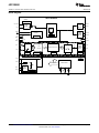
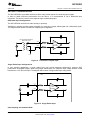
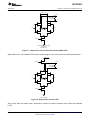
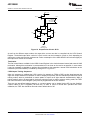
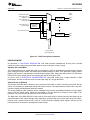
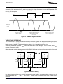
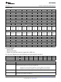
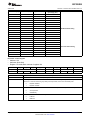
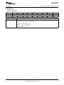
1
ADC12EU050
www.ti.com
SNAS444I – JANUARY 2008 – REVISED APRIL 2013
ADC12EU050 Ultra-Low Power, Octal, 12-bit, 45 MSPS Sigma-Delta Analog-to-Digital
Converter
Check for Samples: ADC12EU050
FEATURES
1
•
•
•
•
•
•
•
•
2
™
Xignal CT∑Δ ADC Technology
45MSPS Sampling Rate
Anti-Alias Filter Free Nyquist Sample Range
Unique Instant Overload Recovery (IOR)
Wide 2.10 VPP Input Range
1.2V Supply Voltage
Integrated Precision LC PLL
Serial Control via SPI Compatible Interface
APPLICATIONS
•
•
•
•
Medical Imaging, Ultrasound
Industrial Ultrasound, such as Non-Destructive
Testing
Communications
Battery Powered Portable Systems
KEY SPECIFICATIONS
•
•
•
•
•
•
•
•
DESCRIPTION
The ADC12EU050 is a 12-bit, ultra-low power, octal
A/D converter for use in high performance analog to
digital applications. The ADC12EU050 uses an
innovative continuous time sigma delta architecture
offering ultra low power consumption and an alias
free sample bandwidth up to 22.5MHz. The input
stage of each channel features a proprietary system
to ensure instantaneous recovery from overdrive.
Instant overload recovery (IOR) with no memory
effect ensures the elimination of phase errors
resulting from out of range input signals. The
ADC12EU050 reduces interconnection complexity by
using programmable serialized outputs which offer
the industry standard LVDS and SLVS modes. Power
consumption of only 46mW per channel @ 45MSPS
gives a total chip power consumption of 364mW. The
ADC12EU050 can operate entirely from a 1.2V
supply, although a separate output driver supply of up
to 1.8V can be used. The device operates from 0 to
+70 °C and is supplied in a 10 x 10 mm2, 68-pin
VQFN package.
Resolution 12 Bits
Conversion Rate 45 MSPS
SNR : 69.3 dBFS (typ) @ 45 MSPS
fIN = 4.4MHz
THD –76.6 dB (typ) @ 45 MSPS
fIN = 4.4MHz
Per Channel Power 46 mW/ch (typ) @ 45 MSPS
Total Active Power 364 mW (typ) @ 45 MSPS
Inter-Channel Isolation >110 dB @
fIN = 4.4 MHz
Operating Temp. Range 0 to +70 °C
1
2
Please be aware that an important notice concerning availability, standard warranty, and use in critical applications of
Texas Instruments semiconductor products and disclaimers thereto appears at the end of this data sheet.
All trademarks are the property of their respective owners.
PRODUCTION DATA information is current as of publication date.
Products conform to specifications per the terms of the Texas
Instruments standard warranty. Production processing does not
necessarily include testing of all parameters.
Copyright © 2008–2013, Texas Instruments Incorporated
ADC12EU050
SNAS444I – JANUARY 2008 – REVISED APRIL 2013
www.ti.com
Block Diagram
ADC12EU050
CMOS IN
CLK+ (SE)
PLL
LVDS
Input
CLK-
Output
LVDS
SLVS
BCLK+
BCLK-
LC
VCO
ADC
CONTROL
SLEEP
RST
Output
LVDS
SLVS
Register
1.2V
VA
Register
WCLK+
WCLK-
AGND
1.2V to 1.8V
1.2V
VD
DGND
DGND
Clipping Control
VINn+
12 bit
3 bit
1.3 kÖ
Serializer
CTÐ?
Digital Decimation Filter
Modulator
VINn-
Register
Register
Register
DCAP
RREF
IRef
DOn+
DOn-
Register
SPI Control
To Registers
0.5V
DC
Ref
select
Register
SDATA
2
Output
LVDS
SLVS
8 times
Reference and Bias
VREFB
1 bit
1.3 kÖ
Register
VREFT
VDR
Submit Documentation Feedback
SCLK
SSEL
Copyright © 2008–2013, Texas Instruments Incorporated
Product Folder Links: ADC12EU050
ADC12EU050
www.ti.com
SNAS444I – JANUARY 2008 – REVISED APRIL 2013
VIN1-
VIN1+
VA
VIN2-
VIN2+
VA
VIN3-
VIN3+
VA
VIN4-
VIN4+
VA
VIN5-
VIN5+
VA
VIN6-
VIN6+
Connection Diagram
68
67
66
65
64
63
62
61
60
59
58
57
56
55
54
53
52
VA
1
51 VA
VIN0+
2
50 VIN7-
VIN0-
3
49 VIN7+
VREFB
4
48 CLK-
VREFT
5
47 CLK+ (SE)
DCAP
6
46 SSEL
RREF
7
45 SCLK
ADC12EU050
VA
8
RST
9
44 SDATA
43 VD
Pin 0 - AGND
Exposed pad
(rear of package)
SLEEP 10
42 VD
VD 11
41 DGND
VD 12
40 DGND
DGND 13
39 WCLK-
DGND 14
38 WCLK+
DO0+ 15
37 BCLK-
DO0- 16
36 BCLK+
29
30
31
32
33
34
DO7-
28
DO7+
DO3+
27
DO6-
DGND
26
DO6+
DO2-
25
DGND
DO2+
24
DO5-
23
DO5+
22
VDR
21
DO4-
20
DO4+
19
DO3-
18
DO1-
35 VDR
DO1+
VDR 17
Figure 1. 68-Pin VQFN
See NKE0068A Package
Submit Documentation Feedback
Copyright © 2008–2013, Texas Instruments Incorporated
Product Folder Links: ADC12EU050
3
ADC12EU050
SNAS444I – JANUARY 2008 – REVISED APRIL 2013
www.ti.com
PIN DESCRIPTIONS
Pin No.
Name
Type
Function and Connection
Input
Differential analog inputs to the ADC, for channels 0 to 7. The
negative input pin may be connected via a capacitor to AGND or the
inputs may be transformer coupled for single ended operation.
Differential inputs are recommended for best performance.
ANALOG I/O
2
3
67
68
64
65
61
62
58
59
55
56
52
53
49
50
VIN0+
VIN0VIN1+
VIN1VIN2+
VIN2VIN3+
VIN3VIN4+
VIN4VIN5+
VIN5VIN6+
VIN6VIN7+
VIN7-
4
VREFB
Optional negative reference voltage to improve multi-channel ADC
matching. This pin must be connected to AGND.
VREFT
Optional positive reference voltage to improve multi-channel ADC
matching. If using the internal reference, this pin should be left tied
to AGND through a 100nF capacitor. If using an external reference
voltage, this pin should be connected to the positive reference
voltage, which must lie in the range specified in the Electrical
Characteristics table.
6
DCAP
Input
This pin provides the capacitance for the low pass filter in the
modulator’s DAC. It must be connected to AGND through a minimum
100nF capacitor. It is possible to decrease the noise close to the
carrier by increasing this capacitor, up to a maximum of 10μF. See
APPLICATION INFORMATION for further information on the
selection of this capacitor.
7
RREF
Input/Output
External bias reference resistor. This pin must always be connected
to AGND through a resistor, whether the internal reference or an
external reference voltage is used. The resistor value must be 10kΩ
±1%.
9
RST
Input
This pin is an active low reset for the entire ADC, both analog and
digital components. The pin must be held low for 500ns then
returned to high in order to ensure that the chip is reset correctly.
10
SLEEP
Input
Sleep mode. Toggling this pin to high will cause the ADC to enter the
low power sleep mode. When the pin is returned to low, the chip will,
after the specified time to exit sleep mode, return to normal
operation.
15
16
18
19
20
21
23
24
25
26
28
29
31
32
33
34
DO0+
DO0DO1+
DO1DO2+
DO2DO3+
DO3DO4+
DO4DO5+
DO5DO6+
DO6DO7+
DO7-
Output
Differential Serial Outputs for channels 0 to 7. Each pair of outputs
provides the serial output for the specific channel. The default output
is reduced common mode LVDS format, but by programming the
appropriate control registers, the output format can be changed to
SLVS or LVDS.
By programming TX_term (bit 4) in the LVDS Control register, it is
possible to internally terminate these outputs with 100 ohm resistors.
36
37
BCLK+
BCLK-
Output
Bit clock. Differential output clock used for sampling the serial
outputs. Information on timing can be seen in the ELECTRICAL
CHARACTERISTICS.
By programming TX_term (bit 4) in the LVDS Control register, it is
possible to internally terminate these outputs with 100 ohm resistors.
5
DIGITAL I/O
4
Submit Documentation Feedback
Copyright © 2008–2013, Texas Instruments Incorporated
Product Folder Links: ADC12EU050
ADC12EU050
www.ti.com
SNAS444I – JANUARY 2008 – REVISED APRIL 2013
PIN DESCRIPTIONS (continued)
Pin No.
Name
Type
Function and Connection
38
39
WCLK+
WCLK-
Output
Word Clock. Differential output frame clock. Information on timing
can be seen in ELECTRICAL CHARACTERISTICS.
By programming TX_term (bit 4) in the LVDS Control register, it is
possible to internally terminate these outputs with 100 ohm resistors.
44
SDATA
Input/Output
SPI data input and output. This pin is used to send and receive SPI
address and data information. The direction of the pin is controlled
internally by the ADC based on the SPI protocol.
45
SCLK
Input
SPI clock. In order to use the SPI interface, a clock must be provided
on this pin. See ELECTRICAL CHARACTERISTICS for SPI clock
and timing information.
46
SSEL
Input
SPI chip select. This active low pin is used to enable the serial
interface.
47
48
CLK+ (SE)
CLK-
Input
Differential Input Clock. The input clock must be 45MHz. It is used
by the PLL to generate the internal sampling clocks. A single ended
clock can also be used, and should be connected to pin 47.
1, 8, 51, 54,
57, 60, 63,
66
VA
Power
Analog Power Supply. All pins should be connected to the same
1.2V supply, with voltage limits as in the Electrical Specification.
POWER SUPPLY
0
AGND
Ground
Analog Ground Return.
11, 12, 42,
43
VD
Power
Digital Power Supply. Connect to 1.2V, with voltage limits as in the
Electrical Specification.
13, 14, 22,
30, 40, 41
DGND
Ground
Digital and Output Driver Ground Return.
17, 27, 35
VDR
Power
Output Driver Power Supply. Can be connected to 1.2V – 1.8V,
depending on application requirements. Voltage limits are described
in more detail in the Electrical Specification.
These devices have limited built-in ESD protection. The leads should be shorted together or the device placed in conductive foam
during storage or handling to prevent electrostatic damage to the MOS gates.
ABSOLUTE MAXIMUM RATINGS
(1) (2)
Supply Voltage (VA, VD)
−0.3V to 1.4V
IO Supply Voltage (VDR)
-0.3 to 2.0V
Voltage at Analog Inputs
-0.3 to 1.4V
Voltage at SPI Inputs
-0.3 to 2.5V
Input Current, VIN+, VIN-
±1mA
Input Current, other pins
ESD Susceptibility
±10mA
Human Body Model
2000V
Machine Model
200V
Charged Device Mode
Soldering Temperature
1,000V
Infrared, 10 seconds
235°C
−65°C to +125°C
Storage Temperature Range
Soldering process must comply with Texas Instruments' Reflow Temperature Profile specifications. Refer to www.ti.com/packaging.
(1)
(2)
Absolute maximum ratings are those values beyond which the safety of the device cannot be ensured. They are not meant to imply that
the device should be operated at these limits.
All voltages are measured with respect to GND = AGND = DGND = 0V, unless otherwise specified.
Submit Documentation Feedback
Copyright © 2008–2013, Texas Instruments Incorporated
Product Folder Links: ADC12EU050
5
ADC12EU050
SNAS444I – JANUARY 2008 – REVISED APRIL 2013
OPERATING RATINGS
www.ti.com
(1) (2)
Operating Temperature Range
0°C to +70°C
Supply Voltage (VA=VD)
+1.16 to +1.26V
IO Supply Voltage (VDR)
+1.16 to +1.89V
Minimum rise time on VA, VD, VDR at power-up
40µs
Analog Inputs (VINN+, VINN-)
-0.10 to VA
SPI Inputs (SDATA, SSEL, SCLK)
+1.16 to +2.50V
VREFT (When using external reference)
475mV to 525mV
VREFB
AGND
VCM Input Common Mode Range (Differential Input)
0.4V to 1.2V
Ground Difference |AGND-DGND|
(1)
(2)
<50mV
Operating Ratings indicate conditions for which the device is specified to be functional, but do not specify specific performance limits.
Specifications and test conditions are specified in the Electrical Characteristics section. Operation of the device beyond the Operating
Ratings is not recommended as it may degrade the device lifetime.
All voltages are measured with respect to GND = AGND = DGND = 0V, unless otherwise specified.
ELECTRICAL CHARACTERISTICS
Unless otherwise specified, the following conditions apply: VA = VD = 1.2V; VDR = 1.2V; VREF = internal; RREF = 10kohm ±1%;
CL = 5pF; 100Ω terminated at the receiver; fCLK = 45MHz; fS = 45MSPS. Boldface limits apply for TA = TMIN to TMAX; All other
limits apply for TA = +25°C.
Symbol
Parameter
Typical (1)
Conditions
Limits
Units
12
Bits
LSB
Static Converter Characteristics
Resolution (No missing codes
ensured)
INL
Integral Non Linearity
±0.75
±3.0
DNL
Differential Non Linearity
±0.35
±0.75
LSB
PSE
Positive Full Scale Error
±0.66
±3
%FS
NSE
Negative Full Scale Error
±0.58
±3
%FS
GE
Gain Error
±1.23
%FS
Dynamic Converter Characteristics – Instant Overload Recovery (IOR) Off
SNR
Signal to Noise Ratio (2)
SINAD
Signal to Noise and Distortion (2)
ENOB
Effective Number of Bits
THD
Total Harmonic Distortion
H2
Second Harmonic Distortion
H3
Third Harmonic Distortion
SFDR
Spurious Free Dynamic Range
IMD
Intermodulation Distortion
(1)
(2)
6
fCLK = 45MHz, fIN = 4.4MHz, VIN = -0.5dBFS
69.3
fCLK = 45MHz, fIN = 9.5MHz, VIN = -0.5dBFS
69.0
fCLK = 45MHz, fIN = 4.4MHz, VIN = -0.5dBFS
68.5
fCLK = 45MHz, fIN = 9.5MHz, VIN = -0.5dBFS
68.5
fCLK = 45MHz, fIN = 4.4MHz, VIN = -0.5dBFS
11.1
fCLK = 45MHz, fIN = 9.5MHz, VIN = -0.5dBFS
11.1
fCLK = 45MHz, fIN = 4.4MHz, VIN = -0.5dBFS
-76
fCLK = 45MHz, fIN = 9.5MHz, VIN = -0.5dBFS
-78
fCLK = 45MHz, fIN = 4.4MHz, VIN = -0.5dBFS
-81
fCLK = 45MHz, fIN = 9.5MHz, VIN = -0.5dBFS
-79
fCLK = 45MHz, fIN = 4.4MHz, VIN = -0.5dBFS
-83
fCLK = 45MHz, fIN = 9.5MHz, VIN = -0.5dBFS
-97
fCLK = 45MHz, fIN = 4.4MHz, VIN = -0.5dBFS
77
fCLK = 45MHz, fIN = 9.5MHz, VIN = -0.5dBFS
78
dBc
-70
dBFS
f1 = 9.6MHz, VIN = -6dBFS
f2 = 10.1MHz, VIN = -6dBFS
67.0
dBFS (min)
62.5
dBFS (min)
dBFS
dBFS
10.1
Bits (min)
-65
dBc (max)
Bits
dBc
-66
dBc (max)
-67
dBc (max)
66
dBc (min)
dBc
dBc
Typical figures are at TA = 25°C, and represent most likely parametric norms at the time of product characterization. The typical
specifications are not ensured.
This parameter is specified in dBFS. This indicates the value which would be obtained with a full-scale input.
Submit Documentation Feedback
Copyright © 2008–2013, Texas Instruments Incorporated
Product Folder Links: ADC12EU050
ADC12EU050
www.ti.com
SNAS444I – JANUARY 2008 – REVISED APRIL 2013
ELECTRICAL CHARACTERISTICS (continued)
Unless otherwise specified, the following conditions apply: VA = VD = 1.2V; VDR = 1.2V; VREF = internal; RREF = 10kohm ±1%;
CL = 5pF; 100Ω terminated at the receiver; fCLK = 45MHz; fS = 45MSPS. Boldface limits apply for TA = TMIN to TMAX; All other
limits apply for TA = +25°C.
Symbol
Typical (1)
Limits
Units
fCLK = 45MHz, fIN = 4.4MHz, VIN = -0.5dBFS
67.6
65.5
dBFS (min)
fCLK = 45MHz, fIN = 9.5MHz, VIN = -0.5dBFS
67.4
fCLK = 45MHz, fIN = 4.4MHz, VIN = -0.5dBFS
67.0
61.5
dBFS (min)
fCLK = 45MHz, fIN = 9.5MHz, VIN = -0.5dBFS
67.0
fCLK = 45MHz, fIN = 4.4MHz, VIN = -0.5dBFS
10.8
fCLK = 45MHz, fIN = 9.5MHz, VIN = -0.5dBFS
10.8
fCLK = 45MHz, fIN = 4.4MHz, VIN = -0.5dBFS
-76
fCLK = 45MHz, fIN = 9.5MHz, VIN = -0.5dBFS
-77
fCLK = 45MHz, fIN = 4.4MHz, VIN = -0.5dBFS
-80
fCLK = 45MHz, fIN = 9.5MHz, VIN = -0.5dBFS
-78
fCLK = 45MHz, fIN = 4.4MHz, VIN = -0.5dBFS
-83
fCLK = 45MHz, fIN = 9.5MHz, VIN = -0.5dBFS
-96
fCLK = 45MHz, fIN = 4.4MHz, VIN = -0.5dBFS
76
fCLK = 45MHz, fIN = 9.5MHz, VIN = -0.5dBFS
77
dBc
-70
dBFS
Parameter
Conditions
Dynamic Converter Characteristics – Instant Overload Recovery (IOR) On
SNR
Signal-to-Noise Ratio (3)
SINAD
Signal-to-Noise and Distortion (3)
ENOB
Effective Number of Bits
THD
Total Harmonic Disortion
H2
Second Harmonic Distortion
H3
Third Harmonic Distortion
SFDR
Spurious Free Dynamic Range
IMD
Intermodulation Distortion
f1 = 9.6MHz, VIN = -6dBFS
f2 = 10.1MHz, VIN = -6dBFS
dBFS
dBFS
9.9
Bits (min)
-64
dBc (max)
Bits
dBc
-65
dBc (max)
-67
dBc (max)
65
dBc (min)
dBc
dBc
Inter-channel Characteristics
Channel to channel gain match
Inter-channel Isolation
VIN
Full Scale Analog Input Voltage
Maximum Input for Instantaneous
Recovery from Overload
RIN
VCM
±0.1
fIN = 4.4MHz @ -0.1dBFS
dB
IOR mode off
2.10
VPP
IOR mode on
1.56
VPP
IOR mode on, fIN < 12MHz
2.61
Generated internally
Input Impedance of VReft
VREFOUT
IA
Internal Reference Voltage
Analog Supply Current
dB
110
Adjacent channel terminated
Differential Input Impedance
Internal Input Common Mode
±0.5
605
2.75
VPP (max)
2.4
kΩ (min)
2.8
kΩ (max)
574
mV (min)
637
mv (max)
480
mV (min)
520
mV (max)
20
Generated internally
502
kΩ
fCLK = 45 MHz
147
163
mA (max)
Power Characteristics
ID
Digital Supply Current
fCLK = 45 MHz
123
147
mA (max)
IDR
Output Driver Supply Current
LVDS, VDR = 1.8V, fCLK = 45 MHz
37
45
mA (max)
Power consumption
fCLK = 45 MHz, Equalizer off
364
412
mW (max)
fCLK = 45 MHz, Equalizer on
409
470
mW (max)
Sleep
40
50
mW (max)
Power Down
5
15
mW (max)
fCLK = 45 MHz, Equalizer off
46
mW
fCLK = 45 MHz, Equalizer off
51
mW
Per channel power consumption
PSRR
Power supply rejection ratio
100mV, 100kHz to 1MHz sinusoid on VA
65
dB
CMRR
Common mode rejection ratio
100mV, 1MHz sinusoid on VIN+ and VIN-
60
dB
(3)
This parameter is specified in dBFS. This indicates the value which would be obtained with a full-scale input.
Submit Documentation Feedback
Copyright © 2008–2013, Texas Instruments Incorporated
Product Folder Links: ADC12EU050
7
ADC12EU050
SNAS444I – JANUARY 2008 – REVISED APRIL 2013
www.ti.com
ELECTRICAL CHARACTERISTICS (continued)
Unless otherwise specified, the following conditions apply: VA = VD = 1.2V; VDR = 1.2V; VREF = internal; RREF = 10kohm ±1%;
CL = 5pF; 100Ω terminated at the receiver; fCLK = 45MHz; fS = 45MSPS. Boldface limits apply for TA = TMIN to TMAX; All other
limits apply for TA = +25°C.
Symbol
Parameter
Conditions
Typical (1)
Limits
Units
Recovery time from sleep
12
µs (max)
Recovery time from power down
18
ms (max)
Recovery time from single channel
power down
6
µs (max)
DIGITAL DECIMATION FILTER CHARACTERISTICS
Unless otherwise specified, the following conditions apply: VA = VD = 1.2V; VDR = 1.2V; VREF = internal; RREF = 10kohm ±1%;
CL = 5pF; 100Ω terminated at the receiver; fCLK = 45MHz; fS = 45MSPS. Boldface limits apply for TA = TMIN to TMAX; All other
limits apply for TA = +25°C.
Symbol
Conditions (1)
Parameter
Typical (2
)
Pass Band
fCLK = 45MHz
19.8
Pass Band Transition
fCLK = 45MHz, -3dB attenuation
22.5
Pass Band Ripple
fIN < 22MHz
Stop Band Begin
fCLK = 45MHz
(1)
(2)
MHz
31.05
fIN < 22MHz, Equalizer on
Units
MHz
±0.01
Stop Band Attenuation
Group Delay Ripple (peak to peak)
Limits
dB
MHz
72
dB (min)
0.05
Samples (max)
As the filter is a digital circuit, Digital Decimation Filter Characteristics scale with input clock frequency, fCLK.
Typical figures are at TA = 25°C, and represent most likely parametric norms at the time of product characterization. The typical
specifications are not ensured.
EXTERNAL INPUT CLOCK AND PLL CHARACTERISTICS
Unless otherwise specified, the following conditions apply: VA = VD = 1.2V; VDR = 1.2V; VREF = internal; RREF = 10kohm ±1%;
CL = 5pF; 100Ω terminated at the receiver; fCLK = 45MHz; fS = 45MSPS. Boldface limits apply for TA = TMIN to TMAX; All other
limits apply for TA = +25°C.
Symbol
Parameter
Conditions
Typical (1)
Limits
Units
45
MHz (min)
45.5
MHz (max)
20
% (min)
80
% (max)
External Input Clock
fCLK
Allowed input clock frequency
tCLK
Allowed input clock period
1/fCLK
fCLK DC
Allowed input clock duty cycle
tJIN
Allowed RMS clock jitter on input
clock.
Integrated from 10Hz to BWloop
VCMCLK
Allowed input clock common mode
See
VICLK
Allowed input clock voltage swing
50
300
(2)
Differential clock input.
(2)
ns
fs rms
400
mV (min)
VDR
mV (max)
200
mV peak-peak
(min)
VDR
mV peak-peak
(max)
400
PLL
f∑Δ
(1)
(2)
8
Over-sampling frequency
712
MHz (min)
728
MHz (max)
Typical figures are at TA = 25°C, and represent most likely parametric norms at the time of product characterization. The typical
specifications are not ensured.
The combination of common mode and voltage swing on the clock input must ensure that the positive voltage peaks are not above VDR
and the negative votlage peaks are not below AGND.
Submit Documentation Feedback
Copyright © 2008–2013, Texas Instruments Incorporated
Product Folder Links: ADC12EU050
ADC12EU050
www.ti.com
SNAS444I – JANUARY 2008 – REVISED APRIL 2013
EXTERNAL INPUT CLOCK AND PLL CHARACTERISTICS (continued)
Unless otherwise specified, the following conditions apply: VA = VD = 1.2V; VDR = 1.2V; VREF = internal; RREF = 10kohm ±1%;
CL = 5pF; 100Ω terminated at the receiver; fCLK = 45MHz; fS = 45MSPS. Boldface limits apply for TA = TMIN to TMAX; All other
limits apply for TA = +25°C.
Symbol
Parameter
BWloop
PLL Loop filter bandwidth
tJ
RMS Clock Jitter on Bit Clock output
Conditions
Typical (1)
Limits
Units
Low Bandwidth
400
kHz
High Bandwidth
1.4
MHz
2
ps peak
DIGITAL INPUT AND OUTPUT CHARACTERISTICS
Unless otherwise specified, the following conditions apply: VA = VD = 1.2V; VDR = 1.2V; VREF = internal; RREF = 10kohm ±1%;
CL = 5pF; 100Ω terminated at the receiver; fCLK = 45MHz; fS = 45MSPS. Boldface limits apply for TA = TMIN to TMAX; All other
limits apply for TA = +25°C.
Symbol
Parameter
Conditions
Typical (1)
Limits
Units
Digital Inputs (SDATA, SSEL, SCLK, SLEEP, RST)
VIH
Logical input “1” voltage
Test run at 2MHz
900
mV (min)
VIL
Logical input “0” voltage
Test run at 2MHz
300
mV (max)
IIN1
Logical "1" Input current
1
µA (max)
IIN0
Logical "0" Input current
-1
µA (min)
CIN
Input Capacitance
Specified by design
5
pF
Digital Outputs (SDATA)
VOH
Logical output “1” voltage
Test run at 2MHz, VDR = 1.2V
VDR
850
mV (min)
VOL
Logical output “0” voltage
Test run at 2MHz, VDR = 1.2V
DRGND
250
mV (max)
IOH
Logical "1" Output Current
-0.75
mA (min)
IOL
Logical "0" Output Current
1
mA (max)
Output Drive Capability (SDATA)
CLOAD
Load capacitance
R = 4.7 kohm, VDR > 1.8V
50
pF
R = 4.7 kohm, VDR = 1.2V
50
pF
Open Drain Mode
VEXT
Maximum allowed external voltage on
Open Drain mode activated
SDATA
RSDATA
Recommended SDATA external pull-up
Open Drain mode activated
resistor
(1)
2.5
4.7
V
kΩ
Typical figures are at TA = 25°C, and represent most likely parametric norms at the time of product characterization. The typical
specifications are not ensured.
Submit Documentation Feedback
Copyright © 2008–2013, Texas Instruments Incorporated
Product Folder Links: ADC12EU050
9
ADC12EU050
SNAS444I – JANUARY 2008 – REVISED APRIL 2013
www.ti.com
AC AND TIMING CHARACTERISTICS
Unless otherwise specified, the following conditions apply: VA = VD = 1.2V; VDR = 1.2V; VREF = internal; RREF = 10kohm ±1%;
CL = 5pF; 100Ω terminated at the receiver; fCLK = 45MHz; fS = 45MSPS. Boldface limits apply for TA = TMIN to TMAX; All other
limits apply for TA = +25°C.
Symbol
Parameter
Typical (1)
Conditions
Limits
Units
44.5
MSPS (min)
45.5
MSPS (max)
General ADC Output Timing Parameters
fs
Sample Rate
Conversion Latency
19
Samples
ns
tBCLK
Bit clock period
fCLK = 45MHz
3.7
tWCLK
Word clock period
fCLK = 45MHz
22.2
tS
Outputs Data Edge to Output Clock
Edge Setup Time
fCLK = 45MHz
800
325
ps (min)
tH
Output Data Edge to Output Clock
Edge Hold Time
fCLK = 45MHz
850
470
ps (min)
tDV
Output Data Valid Window
fCLK = 45MHz
1380
885
ps (min)
tR, tF
Output Rise/Fall time
fCLK = 45MHz
320
tDFS
Data Edge to Word Edge Skew
fCLK = 45MHz
-295
(2)
ns
ps (min)
-720
ps (min)
220
ps (max)
LVDS Output Parameters, OCM = 0 (VDR = 1.2V)
VOD
Differential Output Voltage
VOCM
Output Common Mode Voltage
LVDS mode, I_drive[1:0] = 00 (2.5mA), RL
= 100Ω
270
LVDS mode, I_drive[1:0] = 01 (3.5mA), RL
= 100Ω
370
LVDS mode, I_drive[1:0] = 11 (5.0mA), RL
= 100Ω
520
LVDS mode, OCM = 0 (for VDR = 1.2V)
945
mV
318
mV (min)
428
mV (max)
mV
895
mV (min)
1000
mV (max)
LVDS Output Parameters, OCM = 1 (VDR = 1.8V)
VOD
Differential Output Voltage
VOCM
Output Common Mode Voltage
LVDS mode, I_drive[1:0] = 00 (2.5mA), RL
= 100Ω
265
LVDS mode, I_drive[1:0] = 01 (3.5mA), RL
= 100Ω
350
LVDS mode, I_drive[1:0] = 11 (5.0mA), RL
= 100Ω
485
LVDS mode, OCM = 1
1265
mV
280
mV (min)
417
mV (max)
mV
1200
mV (min)
1340
mv (max)
SLVS Output Parameters
VOD
Differential Output Voltage
VOCM
(1)
(2)
10
Output Common Mode Voltage
SLVS mode, I_drive[1:0] = 00 (2.5mA), RL
= 100Ω
245
SLVS mode, I_drive[1:0] = 01 (3.5mA), RL
= 100Ω
330
SLVS mode, I_drive[1:0] = 11 (5.0mA), RL
= 100Ω
475
SLVS mode
225
mV
262
mV (min)
393
mV (max)
mV
185
mV (min)
270
mV (max)
Typical figures are at TA = 25°C, and represent most likely parametric norms at the time of product characterization. The typical
specifications are not ensured.
This parameter is specified by design and/or characterization and is not tested in production.
Submit Documentation Feedback
Copyright © 2008–2013, Texas Instruments Incorporated
Product Folder Links: ADC12EU050
ADC12EU050
www.ti.com
SNAS444I – JANUARY 2008 – REVISED APRIL 2013
AC AND TIMING CHARACTERISTICS (SERIAL INTERFACE)
Unless otherwise specified, the following conditions apply: VA = VD = 1.2V; VDR = 1.2V; VREF = internal; RREF = 10kohm ±1%;
CL = 5pF; 100Ω terminated at the receiver; fCLK = 45MHz; fS = 45MSPS. Boldface limits apply for TA = TMIN to TMAX; All other
limits apply for TA = +25°C.
Symb
ol
Parameter
Typical (1)
Conditions
Limits
Units
Serial Interface
tSSELS
SSEL setup time
250
tSSELH
SSEL hold time
250
ns
tWS
SDATA setup time, write transaction
250
15
ns (max)
tWH
SDATA hold time, write transaction
250
10
ns (max)
tSCLK
SCLK period
1
0.2
µs (min)
tSCLKL
SCLK low time
ns
450
ns (min)
tSCLKH SCLK high time
450
ns (min)
tSCLKR SCLK rise time
50
ns
tSCLKF
50
ns
500
ns
SCLK fall time
tSSELHI SSEL high time
Applies to read and write transactions
tRS
SDATA valid setup time, read
transaction
100
-5
ns (min)
tRH
SDATA valid hold time, read transaction
250
10
ns (min)
(1)
Typical figures are at TA = 25°C, and represent most likely parametric norms at the time of product characterization. The typical
specifications are not ensured.
TIMING DIAGRAMS
System Clock
tWCLK
WCLK-
Word Clock
WCLK+
tBCLK
BCLK+
Bit Clock
BCLKtR
tH
tDV
tF
DOn+
Output data
D10 D11
D0
D1
D2
D3
D4
D5
D6
D7
D8
D9
D10 D11
D0
D1
D2
D3
D4
D5
DOntS
Sample n
Sample n+1
Figure 2. LVDS/SLVS Output Timing
Submit Documentation Feedback
Copyright © 2008–2013, Texas Instruments Incorporated
Product Folder Links: ADC12EU050
11
ADC12EU050
SNAS444I – JANUARY 2008 – REVISED APRIL 2013
www.ti.com
VDR
VOCM + VOD/2
Differential
output signal
VOCM
VOCM - VOD/2
0
Figure 3. Output Level Definitions
tSCLK
tSSELS
tSCLKL
tWH
tSCLKH
SCLK
SDATA
90%
90%
10%
10%
D7
R/W
A7
tSSELH
tSCLKF
tSCLKR
tWS
D0
SSEL
Figure 4. SPI Write Timing
tRH
tSSELHI
tRS
A7
,
SDATA
,
SCLK
D7
D0
SSEL
Figure 5. SPI Read Timing
12
Submit Documentation Feedback
Copyright © 2008–2013, Texas Instruments Incorporated
Product Folder Links: ADC12EU050
ADC12EU050
www.ti.com
SNAS444I – JANUARY 2008 – REVISED APRIL 2013
FUNCTIONAL DESCRIPTION
The ADC12EU050 employs a number of unique strategies to provide a high performance multi-channel ADC that
offers a significant power consumption reduction when compared to compteting architectures, as well as easing
system level design. The ultra-low power performance of the ADC12EU050 is derived from the implementation of
a fast continuous time sigma delta (CT∑Δ) modulator. Other features of this technology are:
• Intrinsic anti-alias filter – the digital decimating filter provides an intrinsic anti-alias filter, eliminating external
analog filter components, and simplifying multi-channel designs.
• Instant overload recovery (IOR) system ensures extremely fast recovery from overload (<1ps), and no settling
errors on return from overload.
• Ultra-low inter-channel crosstalk.
• Digital Equalizer provides low group delay and hence minimizes signal path delay variation.
The major signal path blocks are: clipping control; CT∑Δ modulator; digital decimation filter; 12 bit serializer; and
finally the LVDS/SLVS outputs. The PLL is critical to the operation of the ADC12EU050, and the PLL also
provides the bit and word clock outputs. The SPI Control Interface gives uncomplicated user access to the ADC
registers.
12-BIT SIGMA DELTA ADC CORE
The ADC12EU050 comprises eight analog ADC channels using a CT∑Δ architecture, which provides very high
dynamic performance with ultra-low power, while operating from a minimal 1.2V supply.
The CT∑Δ ADC architecture uses a third order sigma delta modulator operating at a nominal 16 times oversampling rate in combination with a 3-bit quantizer. The modulator output is coupled to a power efficient digital
decimation filter that decimates the high rate modulator output (720MHz) to provide output data at a 45 MSPS
sample rate.
A benefit of the CT∑Δ design is that the ADC requires no external anti-alias filters for most applications. This
benefit is derived from a combination of the design of the analog sigma delta modulator and digital decimation
filter. The digital filter achieves a steep transition band, and provides 72 dB of attenuation in the stop band. Using
the digital equalizer, the signal transfer characteristics including phase performance can be optimized so as to
minimise group delay variation. In applications where it is not required, the digital equalizer can be disabled to
further save power.
DIFFERENTIAL INPUT STAGE
The ADC can capture high speed analog signals without resorting to a complex fast sample-and-hold amplifier
(SHA) as used in pipeline ADCs. This is where CT∑Δ technology derives much of its power and performance
benefits. This feature also assists external circuit design. In the case of the SHA inputs of pipeline ADCs, the
effective input capacitance is time variant, requiring a powerful input buffer to drive to the resolution limits of the
system. The input stage of the ADC is purely resistive (1.3kΩ single ended) driving into virtual earth. As a result
the ADC12EU050 is extremely easy to drive as its input impedance is not complex. It also means that external
lower power input buffering circuitry can used, and can be completely eliminated in some cases.
Submit Documentation Feedback
Copyright © 2008–2013, Texas Instruments Incorporated
Product Folder Links: ADC12EU050
13
ADC12EU050
SNAS444I – JANUARY 2008 – REVISED APRIL 2013
CLK
www.ti.com
CLK
VIN+
CLK
CLK
OPAMP
VIN-
CLK
CLK
Figure 6. SHA Input Stage
VIN+
OPAMP
VIN-
Figure 7. Continuous Time Sigma Delta Input Stage
INSTANT OVERLOAD RECOVERY
The ADC12EU050 features an overload handling system which provides instantaneous recovery from signals
driving the ADC inputs beyond the full-scale input range. The ADC can operate in two different modes. In the
default ADC mode (IOR mode off) a full-scale input range of 2.10 VPP is supported, here the ADC operates with
some inherent overload recovery time, similar to a conventional ADC.
In the IOR mode, the ADC has a reduced 1.56 VPP full scale input range, but provides a significant benefit in that
the ADC can now be driven by input voltages as high as 5 dB beyond the nominal full-scale (fIN < 12MHz), that is
2.75 VPP, and will recover instantaneously. In a number of applications this feature can help simplify input stage
design and manufacturing set-up and calibration. The ADC12EU050 recovers immediately from overload with no
missing codes and no settling time.
The proprietary strategy used within the ADC12EU050 uses high speed patented clamp techniques to limit the
input signal and keep it within the stable input range of the ADC. This process happens at a speed equivalent to
the on-chip over-sampling rate of 720MHz. The advantage of this system is that it responds immediately to out of
range signals. While the inputs are over-range the ADC outputs a full scale result. As the over-range input is
removed the ADC adjusts to the input signal level and is able to provide sampled data instantaneously. The
ADC’s behavior on emerging from overload is repeatable and independent of whether the input signal was
positive or negative going at the point of overload. The diagram below shows a 5dB overloaded input (2.75 VPP
versus 1.56 VPP Full scale), with 240,000 sample periods overlaid. There is no ringing and recovery from
overload is instantaneous.
14
Submit Documentation Feedback
Copyright © 2008–2013, Texas Instruments Incorporated
Product Folder Links: ADC12EU050
ADC12EU050
www.ti.com
SNAS444I – JANUARY 2008 – REVISED APRIL 2013
Figure 8. Instant Overload Recovery
INTEGRATED PRECISION LC PLL
The ADC12EU050 family includes an integrated high performance “clean up” phase locked loop (PLL),
simplifying the need for a low jitter external clock. The PLL serves three important functions; it generates a highly
accurate internal sampling clock source of up to 720 MHz; a clock for the LVDS serializers at 540 MHz; and it
provides a low jitter clock for other internal components. With its jitter clean-up capability this PLL allows lower
performance system clocks to be used.
DIGITAL DECIMATION FILTER AND EQUALIZER
The digital decimation filter is an integral part of the sigma delta architecture. It decimates the over-sampled data
from the modulator down to the sample rate, and its extremely sharp low pass characteristic combined with the
modulator’s broad band response provides the intrinsic anti-alias filter. The digital low pass filter exhibits 72dB of
attenuation in the stop band. The following diagram shows the digital filter transfer function at 40MSPS,
compared to a third order Butterworth transfer function. Due to the digital implementation of the filter, the filter
parameters automatically scale with the ADC sampling frequency.
Figure 9. Digital Filter Transfer Function
Submit Documentation Feedback
Copyright © 2008–2013, Texas Instruments Incorporated
Product Folder Links: ADC12EU050
15
ADC12EU050
SNAS444I – JANUARY 2008 – REVISED APRIL 2013
www.ti.com
Such steep digital filters introduce group delay problems, but the ADC12EU050 includes a digital equalizer,
which reduces group delay ripple variation to less than 0.05 samples. In applications where group delay is not of
concern, the equalizer can be turned off through the SPI interface in order to save power.
The following two diagrams show the group delay ripple of the digital decimation filter at 50MSPS, firstly with the
equalizer disabled, and secondly with the equalizer enabled.
Figure 10. Group Delay with Equalizer Off
Figure 11. Group Delay with Equalizer On
SERIAL DATA OUTPUTS
Sampled data is transformed into high speed serial LVDS/SLVS output data streams. The low amplitude
differential signal swings of LVDS/SLVS help to reduce digital system noise.
It is possible to select between LVDS and SLVS modes by simple programming through the SPI control
interface. The output common mode can also be programmed through the SPI control interface, allowing it to be
adjusted based on the value of VDR.
POWER MANAGEMENT MODES
The ADC12EU050 operates normally at ultra-low power levels. In addition, several power management modes
are provided:
• Power Down (accessible through PD bit of Top Control Register)
• Sleep (SLEEP pin, or SLEEP bit of Top Control Register)
• Single channel power down (PD0-7 of ADC/LVDS Channel Power Down Register)
Power Down is the lowest power consumption mode, but with a longer wake-up time than Sleep mode. In power
down mode, all circuits in the chip are turned off, including the PLL, reference and bias circuits.
Power consumption in Sleep mode is higher than in Power Down mode, but pin access (SLEEP pin) and fast
wake-up enables duty cycle powering of the ADC.
The device also allows channel by channel power-down through the ADC/LVDS Channel Power Down register.
When a single channel is powered down, the sigma delta modulator, digital decimating filter and LVDS outputs
for that channel will be shut off, with the corresponding single channel reduction in power consumption.
SPI CONTROL INTERFACE
The ADC12EU050 provides configurability via the serial control interface. This provides IOR mode control power
management control, output configuration control, data output test patterns to provide LVDS/SLVS training
sequences, as well as many other user configurable options. Full details of the SPI registers can be found in
Programming Guide.
The SPI pins (SDATA, SCLK, SSEL), as well as the pins RST and SLEEP, have been designed to operate with
voltage levels up to 2.5V, despite the low 1.2V core voltage. As a result, no external level shift components are
required for this control interface.
16
Submit Documentation Feedback
Copyright © 2008–2013, Texas Instruments Incorporated
Product Folder Links: ADC12EU050
ADC12EU050
www.ti.com
SNAS444I – JANUARY 2008 – REVISED APRIL 2013
UNCORRELATED NOISE REFERENCE FOR EACH CHANNEL
In many early multi-channel ADC designs, a single voltage reference was used to provide the reference level for
each channel. Unfortunately, this ensures that the noise at each ADC’s reference terminal is cross correlated.
Multi-channel systems often make use of a 3 dB processing gain increase that results from each channel
doubling. Without a specific technique to prevent the reference terminals seeing correlated noise the expected 3
dB gain is compromised. In the case of the ADC12EU050, a unique system has been implemented to decorrelate the noise at each ADC channel.
APPLICATION INFORMATION
POWER-UP SEQUENCE
The ADC12EU050 has three separate power supplies: Analog (VA), Digital (VD) and the output drive voltage (
VDR). The ADC contains a power on reset circuit, connected to VA, and so to ensure correct reset of both analog
and digital logic of the ADC, the power supplies should be provided in the following order:
1. VDR
2. VD
3. VA
If this order is not followed, then the user should issue a reset via the reset pin (RST) immediately after power
up. Additionally, it is required that the rise time for each voltage supply is longer than the minimum rise time
stated in the ELECTRICAL CHARACTERISTICS.
There is no required sequence for powering down the ADC.
ADC START-UP SEQUENCE
After any reset, either power-on reset, software reset via SPI or hardware reset via the RST pin, the chip
undergoes a series of internal calibrations and the PLL/VCO will lock to the external clock.
After reset, the ADC12EU050’s registers have the default values shown in register tables. The registers can be
programmed via the SPI after reset, even during the period while the chip is performing the internal calibrations
mentioned in the previous paragraph.
During reset and until the PLL is locked, the LVDS outputs will not provide valid data. Furthermore, the ADC has
an inherent data conversion latency, which is related to the pipeline stages of the digital decimating filter. Until
the data conversion latency has passed, the data outputs will be invalid.
Thus the maximum time until valid sampled data is received at the outputs is:
PLL lock time + ADC Latency
Specific values for these times can be found in the ELECTRICAL CHARACTERISTICS.
USING ADC LOW POWER MODES
As explained previously in FUNCTIONAL DESCRIPTION, the ADC12EU050 offers several power management
modes.
Sleep mode offers the fastest wake-up time, and should be used in applications where duty cycle powering of the
ADC is required. In this case it is recommended to toggle sleep mode via the SLEEP pin, which will give a faster
cycle time than programming the SLEEP bit through the SPI, due to the extra time required to send a command
through the SPI port.
The Power Down mode is accessible via the SPI port. Due to the power-up time of the ADC coupled with the
programming time of the SPI port, this mode should be used to power the chip down for longer time periods.
Channel power down allows one or more channels to be turned off independently, with the corresponding power
saving.
Submit Documentation Feedback
Copyright © 2008–2013, Texas Instruments Incorporated
Product Folder Links: ADC12EU050
17
ADC12EU050
SNAS444I – JANUARY 2008 – REVISED APRIL 2013
www.ti.com
CLOCK SELECTION CONSIDERATIONS
The ADC12EU050 has an on-chip PLL, which simplifies the task of clock source selection and clock network
design.
Clock Input Connection
The ADC is designed to accept either single ended or differential clock inputs. Furthermore, the clock source can
be a sine or square wave. In order to obtain the best performance, a differential square wave clock should be
used. When using a differential clock, the clock traces should be routed as 100Ω differential pairs, and
terminated with a 100Ω resistor close to the chip. A single ended clock input should be connected to pin 47
(CLK+/SE), and pin 48 (CLK-) should be grounded.
On-chip PLL
The benefit of having an on chip PLL is that in most applications a high precision clock source is not required.
The external clock's contribution to aperture jitter is reduced dramatically by the jitter clean-up properties of the
PLL, which ensures that any RMS jitter outside of the PLL bandwidth is attenuated. The PLL also significantly
relaxes the input clock duty cycle requirements, accepting input clock duty cycles of 20% to 80%.
40
40
20
20
0
0
GAIN (dB)
GAIN (dB)
The PLL offers two choices of bandwidth. For the majority of systems, the default bandwidth of 400kHz is
suitable. If the system already contains a high performance clock, with excellent RMS jitter performance up to a
1.4MHz bandwidth, then the PLL’s high bandwidth mode may be used.
-20
-40
-20
-40
-60
-60
Loop Bandwidth at 0.415 MHz
Loop Bandwidth at 1.50 MHz
-80
1
10
10
2
10
3
10
4
5
10
10
6
10
7
Loop Bandwidth at 0.380 MHz
Loop Bandwidth at 1.280 MHz
8
10
-80
1
10
OFFSET (Hz)
10
2
10
3
10
4
5
10
10
6
10
7
8
10
OFFSET (Hz)
Figure 12. PLL Phase Noise Transfer Function: fs =
40MHz
Figure 13. PLL Phase Noise Transfer Function: fs =
50MHz
On the input clock, excessive RMS jitter within the PLL bandwidth will be seen in the output spectrum as
sidebands, or close in phase noise, around the fundamental signal.
Input Clock Selection
For systems which do not have a requirement for a high performance clock, any standard product 45MHz crystal
oscillator will allow the ADC12EU050 to perform to specifications. If the system requires high performance clocks
for other system components, then Texas Instruments' LMK family of clock conditioners are recommended.
Output Clock Synchronization Across Multiple Chips
In systems containing more than one ADC12EU050, it is often required that the timing of output samples is
synchronized across the multiple chips. The PLL in the ADC12EU050 takes care of this automatically by aligning
the output clocks with the input clock. The user must ensure, using correct board layout and clock buffering
techniques, that the input clock to each ADC12EU050 is synchronized. If this is the case, then the output frame
clocks will also be synchronized. This means that output samples are aligned.
18
Submit Documentation Feedback
Copyright © 2008–2013, Texas Instruments Incorporated
Product Folder Links: ADC12EU050
ADC12EU050
www.ti.com
SNAS444I – JANUARY 2008 – REVISED APRIL 2013
ADC INPUT CONSIDERATIONS
The ADC12EU050’s sigma delta architecture offers many flexible options for connecting input signals.
In order to obtain maximum performance from the device, it is recommended to use a differential input
connection. The device, however, also supports single ended analog input.
Differential Input Configurations
The ADC12EU050 can be driven either actively or passively.
Transformer coupling provides another possibility for converting a single ended signal into a differential signal.
The diagram below shows a transformer coupled input configuration.
ADC
Recommended transformer:
Mini-circuits T1-6T
VIN+
1st stage
of ÐÂ
Modulator
VIN-
VCM
Figure 14. Transformer Coupled Input
Single Ended Input Configurations
In cost sensitive applications, a single ended input may provide adequate performance, however ADC
performance will degrade slightly. When using single ended inputs, the maximum input voltage allowed is 3dB
less than the 2.10V full scale input. The diagram below shows a single ended input configuration.
ADC
VIN+
VIN-
1st stage
of ÐÂ
Modulator
Figure 15. Single Ended Input
Input Coupling and Common Mode
Submit Documentation Feedback
Copyright © 2008–2013, Texas Instruments Incorporated
Product Folder Links: ADC12EU050
19
ADC12EU050
SNAS444I – JANUARY 2008 – REVISED APRIL 2013
www.ti.com
The ADC12EU050 internally generates a common mode of 0.62V. It is possible to provide input signals with
other common modes however, the full scale input range of the ADC must be kept in mind.
For this reason, it is recommended that the device inputs are AC coupled. The recommended capacitor value is
100nF.
External Series Resistance
Due to the purely resistive input circuit of the sigma delta architecture, the ADC12EU050 allows the user to scale
down large input signals by adding external series resistors. The gain achieved by adding external resistors can
be calculated as a simple voltage divider, as follows:
VFS/VIN = 20 * log (RADC /( RADC + REXT)) dB
(1)
The diagram below shows this configuration, and defines the values in the equation above.
ADC
REXT
Differential
Input p
VIN+
Differential
Input n
VIN-
1st stage
of ÐÂ
Modulator
REXT
Figure 16. External Series Resistance
RADC, the input resistance of the ADC, is nominally 1.3kΩ. Due to manufacturing the value of this resistance can
vary by up to 15%. This is not important for the operation of the ADC, since the ADC depends only on internal
resistors being matched, but it should be taken into account when performing calculations.
ADC OUTPUT CONSIDERATIONS
The ADC12EU050 offers a variety of output settings in order to cater for different system design and integration
needs.
Output Driver Voltage, VDR
The ADC output driver voltage, VDR, can be set between 1.2V and 1.8V. A VDR of 1.2V will offer the lowest
power consumption. Because VDR can be varied, the ADC12EU050 provides, via the SPI registers, the ability to
adjust the output common mode voltage.
Output Modes And Output Common Mode
Three different output modes are also supported: SLVS, LVDS and reduced common mode LVDS. SLVS and
LVDS modes output data according to their respective specifications.
Reduced common mode LVDS must be used when the output driver voltage, VDR, is 1.2V. The standard LVDS
common mode voltage is 1.2V, which is obviously not feasible if VDR is 1.2V. Therefore, the output common
mode voltage must be set to 1.0V by setting the bit OCM in the LVDS Control Register to 0.
20
Submit Documentation Feedback
Copyright © 2008–2013, Texas Instruments Incorporated
Product Folder Links: ADC12EU050
ADC12EU050
www.ti.com
SNAS444I – JANUARY 2008 – REVISED APRIL 2013
VDR = 1.2V
VOUT+
Optional
internal 1005
termination
VOUT-
VIN-
VIN+
VOCM = 1.0V
Bias N
Reduced Common Mode LVDS
Half Bridge
VDD Referenced
Figure 17. Output Driver Circuit: Reduced Common Mode LVDS
When VDR is 1.8V, the standard LVDS common mode voltage of 1.2V must be used, by setting OCM equal to 1.
VDR = 1.8V
VOUT+
Bias P
Optional
internal 1005
termination
VOUT-
VIN-
VIN+
VOCM = 1.25V
Bias N
LVDS
Classic full bridge
Figure 18. Output Driver Circuit: LVDS
SLVS mode offers the lowest power consumption, followed by reduced common mode LVDS then standard
LVDS.
Submit Documentation Feedback
Copyright © 2008–2013, Texas Instruments Incorporated
Product Folder Links: ADC12EU050
21
ADC12EU050
SNAS444I – JANUARY 2008 – REVISED APRIL 2013
www.ti.com
VDR = 1.2V
VOUT+
Bias P
Optional
internal 1005
termination
VOUT-
VIN-
VIN+
VOCM = 175 mV
SLVS
Half Bridge
VSS Referenced
Figure 19. Output Driver Circuit: SLVS
As well as the different output modes, the output drive current can also be controlled via the LVDS Control
Register. The default output drive current is 2.5mA, but this can be increased to 3.5mA or 5mA, depending on
output trace routing and receiver requirements. Power consumption of the ADC12EU050 will increase slightly as
the output driver current is increased.
Termination
The final control feature available in the LVDS Control Register is the choice between internal and external 100Ω
termination. Although the termination is recommended to be as close to the receiver as possible, in some cases
it may be necessary or desirable to perform this termination at the transmitter. Internal 100Ω termination at the
transmitter (the ADC12EU050) is enabled by setting the bit TX_term to 1.
LVDS Output Training Sequences
Often it is necessary to calibrate the LVDS receiver, for example an FPGA or DSP, so that skew between the
eight ADC output channels is minimized. In order to simplify this process, the ADC12EU050 provides three LVDS
training modes, where a pre-defined or custom pattern is output on all eight channels simultaneously. While a
training mode is active, the word and bit clocks are output as usual. In order to select a training mode, the TSEL
bits of the Decimator Control Register (16h) must be programmed via the SPI interface.
There are two pre-defined training patterns, or a custom pattern can be loaded via the SPI into the Serializer
Custom Pattern 0 and 1 Registers (10h and 12h). In order to return to normal ADC operation after skew
calibration, the TSEL bits should be returned to their default value of 00.
22
Submit Documentation Feedback
Copyright © 2008–2013, Texas Instruments Incorporated
Product Folder Links: ADC12EU050
ADC12EU050
www.ti.com
SNAS444I – JANUARY 2008 – REVISED APRIL 2013
ADC
Outputs
CH0 Decimator Output
Training Sequence 1:
000000111111
CH0 Serializer
DO0+
DO0-
CH7 Serializer
DO7+
DO7-
Training Sequence 2:
101010101010
Training Sequence 3:
Custom Pattern
Serializer
Custom Pattern
Registers
10h and 11h
TSEL[0]
TSEL[1]
CH7 Decimator Output
From Decimator
Control Register 16h
Figure 20. LVDS Training Select operation
USING IOR MODE
As discussed in FUNCTIONAL DESCRIPTION, IOR mode provides instantaneous recovery from overload
conditions, with no ringing and correct data output as soon as the input returns in range.
Standard Use of IOR Mode
The recommended way to enable IOR mode is by setting bit 4 (IOR) of the Modulator Overload Control register
(04h). Setting this bit will enable IOR mode with the default settings for DGF in the Decimator Clipping Control
register (14h) and OL in the Modulator Overload Control register (04h). Setting the IOR mode bit to 0 will restore
DGF and OL to their default values, hence putting the chip back into ADC mode.
As can be seen in ELECTRICAL CHARACTERISTICS, using IOR mode gives a slight reduction in SNR
performance, and also a reduction of the full scale input range to 1.56Vpp differential.
Advanced Use of IOR Mode
The registers described above allow the user to customize IOR mode. In order to correctly set the DGF and OL
values, it is necessary to understand how the IOR mode functions. The implementation of IOR mode in the ADC
consists of analog and digital parts working in tandem.
The analog clipping circuitry, controlled by OL, is designed to protect the sigma delta modulator from large signal
inputs. Using an analog clamp, signals are soft-limited to the less than the 2.10Vpp full scale range of the
modulator. OL gives the value at which the circuit will begin to clamp.
The digital filter of the ADC12EU050 is where the full scale input range is selected and the hard limiting of the
signal takes place. DGF selects the gain of the digital filter, and hence the new full scale input range of the ADC.
In order to set a custom value for DGF, CGS, bit 7 of the Decimator Clipping Control register, must be set. The
DGF can then be set, based on the application requirements.
Submit Documentation Feedback
Copyright © 2008–2013, Texas Instruments Incorporated
Product Folder Links: ADC12EU050
23
ADC12EU050
SNAS444I – JANUARY 2008 – REVISED APRIL 2013
www.ti.com
OL should then be set to a value approximately half-way between the new full scale input range (which was just
selected by DGF) and the default full scale input range of 2.10Vpp. OL must be set to a value higher than DGF,
otherwise the signal will be limited by the analog clipping circuitry, rather than the digtal circuitry, and overload
recovery will be impacted.
Input
Output
Analog Clipping
Digital Saturation
IOR Mode full
scale input
1.56 Vpp
differential
Analog sigma delta modulator clips at
voltage selected by OL register.
This protects the Sigma-delta modulator
from overload.
Over-rage input, up to
5 dB above full scale.
Digital Filter saturates at IOR
mode full scale, determined
by DGF register.
Figure 21. IOR Mode Signal Modification
THE VOLTAGE REFERENCE
The ADC provides an on chip, ±5% tolerance voltage reference, together with all necessary biasing circuits and
current sources. A 10kΩ (±1%) resistor must be connected between RREF and AGND in order to establish the
biasing current of the ADC. The internal reference voltage, VREF, is available at the RREF pin.
When using the internal reference, VREFT should be connected to AGND through a 100nF capacitor, while VREFB
must be connected to AGND.
Chip-to-chip gain matching between several ADC12EU050 ADCs can be improved by connecting the VREFT pins
of the ADCs. This is show in the figure below.
10 k5
(± 1%)
10 k5
(± 1%)
VREFB
RREF
VREFT
ADC
n
VREFB
RREF
VREFT
ADC
2
VREFB
VREFT
RREF
ADC
1
10 k5
(± 1%)
AGND
plane
Figure 22. Reference Sharing
If a tighter tolerance reference is required for improved thermal stability, an external voltage reference can be
connected between the VREFT and VREFB pins. The RREF resistor must be connected even when using an external
reference.
24
Submit Documentation Feedback
Copyright © 2008–2013, Texas Instruments Incorporated
Product Folder Links: ADC12EU050
ADC12EU050
www.ti.com
SNAS444I – JANUARY 2008 – REVISED APRIL 2013
DCAP CAPACITOR SELECTION
The DCAP pin provides the capacitance for the low pass filter between the DAC bias block and the DAC in the
sigma-delta modulator. The filter blocks noise from the DAC Bias block from entering the DAC. Any noise which
passes through this filter will be seen in the spectrum as side skirts around the carrier. The filter circuit, which is
a first order RC filter, is shown in the diagram below.
ADC12EU050 ä? Modulator
RDCAP
DAC
Bias
DAC
1.5 k5
DCAP
CDCAP
AGND
Figure 23. DCAP RC Filter
The DCAP pin must be connected to AGND through a low leakage, minimum 100nF capacitor. If the application is
especially sensitive to close to the carrier phase noise, then it is recommended to increase DCAP, up to a
maximum of 10µF. For other applications where close to the carrier phase noise is not important, the capacitor
can be kept small in order to reduce costs and minimise board space. The corner frequency of this filter is
determined by the equation:
f = 1/(2πRDCAPCDCAP)
(2)
BOARD LAYOUT CONSIDERATIONS
Proper grounding, layout and routing are essential to ensure accurate conversion in any high speed ADC.
Maintaining separate analog and digital areas of the board is recommended in order to achieve the specified
performance. This includes using a split ground plane, since the significant digital portion of the chip can produce
noise on the digital/IO ground (DGND).
When designing the ADC12EU050 into a system, It is critical that the exposed pad is connected to analog
ground (AGND). The exposed pad provides the analog ground connection for the ADC12EU050, and so this
connection is required for electrical rather than thermal reasons.
It is recommended to decouple the power supplies using a large capacitor (e.g. 47µF) for low frequency noise,
and small capacitors (e.g. 100nF) placed close to each supply pin.
Analog and digital supplies (VA and VD) may be provided from the same supply, however in this case it is
recommended that the supplies are isolated from each other with a ferrite bead or inductor. If the IO driver supply
(VDR ) is 1.2V, then it may also be taken from the same supply, with isolation as described above.
The clock and data output traces, as well as the clock input trace (when using a differential input clock), should
be routed as 100Ω impedance differential pairs. If not using the option for 100Ω internal termination, then the
clock and data output trances should be terminated with a 100Ω resistor close to the receiver.
If the system requires regulators to provide the ADC12EU050 1.2V operating voltage, Texas Instruments
recommends the LP3878SD-ADJ Low Noise “Ceramic Stable” Adjustable Regulator or the LP3879 Low Noise
“Ceramic Stable” Regulator. Datasheets for both parts are available from the Texas Instruments website.
Submit Documentation Feedback
Copyright © 2008–2013, Texas Instruments Incorporated
Product Folder Links: ADC12EU050
25
ADC12EU050
SNAS444I – JANUARY 2008 – REVISED APRIL 2013
www.ti.com
10 µH
100 nF
100 nF
47 µF
100 nF
100 nF
100 nF
100 nF
VDR
47 µF
47 µF
10 µH
10 µH
VA
VD
Transformer drive circuit.
Other possible drive circuits
shown in Applications
Information.
100 nF
VA
Pins
505
ADT1-6T
VCM
100 nF
100 nF
45 MHz clock. See
Applications
Infomation for more
information on
clocking the
ADC12EU050
VIN0+
VIN0-
DO0+
DO0-
1005
VIN1+
VIN1-
DO1+
DO1-
1005
VIN2+
VIN2VIN3+
VIN3-
DO2+
DO2-
1005
DO3+
DO3-
1005
VIN4+
VIN4VIN5+
VIN5-
DO4+
DO4-
1005
DO5+
DO5-
1005
VIN6+
VIN6VIN7+
VIN7-
DO6+
DO6-
1005
DO7+
DO7-
1005
WCLK+
WCLK-
1005
BCLK+
BCLK-
1005
CLK+ (SE)
CLK100 nF
10 k5 ±1%
VDR
VDR
Pins
VD
Pins
VREFT
VREFB
RREF
Note: External 1005 termination
on the ADC12EU050 is optional.
Internal termination can be
enabled via SPI.
DCAP
10 µF
RST
SLEEP
SSEL
SCLK
SDATA
To SPI
controller
AGND
DGND
Figure 24. ADC12EU050 Application Diagram
26
Submit Documentation Feedback
Copyright © 2008–2013, Texas Instruments Incorporated
Product Folder Links: ADC12EU050
ADC12EU050
www.ti.com
SNAS444I – JANUARY 2008 – REVISED APRIL 2013
Programming Guide
THE SERIAL CONTROL INTERFACE
The ADC12EU050 provides several user controlled functions which are accessed through a standard SPI
compatible, 3 wire Serial Interface, as shown in the diagram below.
output_enable
SPI
controller
(Master)
e.g. DSP,
Microcontroller,
FPGA
serial_out
serial_in
SDATA
clock
SCLK
chip_select_b
SSEL
ADC
Figure 25. Three Wire Control Interface
Wired OR mode is supported in order to connect multiple ADC12EU050 devices to one SPI Master. The clock
and data buses are common to all ADC devices, and the chip select SSEL is used to control which SPI is
currently active. The SPI master must have a unique pin available for each ADC’s SSEL. The diagram below
illustrates the connection.
VD
SPI
Controller
(Master)
output_enable
serial_out
serial_in
clock
e.g. DSP,
Microcontroller, chip_select_b_1
FPGA
chip_select_b_N
SDIO Pads
configured in open
drain mode
SDATA
SCLK
SSEL
ADC
SDATA
SCLK
ADC
SSEL
Figure 26. Multi-Wire Control Interface
When connecting multiple devices, the SDATA pin must be set in Open Drain mode. Open Drain mode is enabled
by setting the SPIOD bit in the Top Control Register of all connected ADC12EU050 devices. When SDATA is in
open drain mode, the user must ensure that a pull-up resistor is connected to the SDATA bus. Further details on
Open Drain mode are given in SDATA PAD OPEN DRAIN MODE.
SERIAL CONTROL INTERFACE PROTOCOL
Both read and write transactions are made up of eight address bits and eight data bits. The final address bit of
the address phase determines whether the transaction will be a read transaction or a write transaction – logic
level low for write, logic level high for read. The following diagram shows the protocol.
Submit Documentation Feedback
Copyright © 2008–2013, Texas Instruments Incorporated
Product Folder Links: ADC12EU050
27
ADC12EU050
SNAS444I – JANUARY 2008 – REVISED APRIL 2013
www.ti.com
SCLK
SSEL
SDATA
A7
A6
A5
A4
A3
A2
A1
R/W
D7
SDATA is driven from externally
D6
D5
D4
D3
D2
D1
D0
If R/W = 1 (read), the SPI drives SDATA.
If R/W = 0 (write), SDATA is driven from externally.
Figure 27. Serial Control Interface Protocol
The eight address bits, A[7:1] + R/W, are sent first. The data, D[7:0], is then sent for a write transaction, or D[7:0]
is received for a read transaction. Address and data are sent and received with the most-significant-bit (MSB)
first. The SPI is enabled using the active low input SSEL. If SSEL is high the SPI cannot be accessed, although
SSEL is not a reset signal and registers will maintain their value when SSEL is toggled. SSEL must be held low
during the entire transaction.
Timing requirements for the Serial Interface are described in ELECTRICAL CHARACTERISTICS.
SERIAL INTERFACE TRANSACTION CANCELLATION
A transaction may be cancelled before the address and data stages are completed by toggling SSEL to high at
any stage during an SPI access. This action is not recommended, as transaction cancellation during a write
transaction may corrupt register contents and during a read transaction will result in incorrect data.
After canceling a transaction with SSEL the ADC may be in an unknown state due to an incomplete and hence
corrupted write to a register. It is therefore recommended to reset the chip via Software Reset (SRES) after a
cancelled transaction.
SDATA PAD OPEN DRAIN MODE
If the SDATA voltage at the board level is required to be higher than the ADC12EU050’s VDR, the Open Drain
mode should be used. In Open Drain mode, the ADC’s SDATA will pull the output low, and SDATA will be pulled up
to the external level by a pull-up resistor connected to the board’s positive voltage rail, VEXT.
The intended use of Open Drain mode is when the ADC, including VDR, is running at 1.2V, and a VEXT of 1.8V
is required.
Open Drain mode is enabled by setting the SPIOD bit in the Top Control Register via the Serial Interface. When
in Open Drain mode, a pull-up resistor (RSDATA) must be connected between SDATA and VEXT. ELECTRICAL
CHARACTERISTICS shows the required settings for VEXT and RSDATA.
SERIAL CONTROL INTERFACE READ AND WRITE SPEED
SCLK (pin 45) controls the speed of interaction with the ADC. The SPI interface supports write to and read from
speeds as defined in the ELECTRICAL CHARACTERISTICS.
SERIAL CONTROL INTERFACE REGISTER DESCRIPTIONS
The following tables show the complete set of user accessible SPI registers, with descriptions of the functionality
of each bit.
Reset values of all registers are also described in the tables below.
28
Submit Documentation Feedback
Copyright © 2008–2013, Texas Instruments Incorporated
Product Folder Links: ADC12EU050
ADC12EU050
www.ti.com
SNAS444I – JANUARY 2008 – REVISED APRIL 2013
Register Index
Address
b[7]
b[6]
b[5]
b[4]
b[3]
b[2]
b[1]
b[0]
Default
Reserved
CBR
Reserved
SRES
SPIOD
SLEEP
PD
00h
PD5
PD4
PD3
PD2
PD1
PD0
00h
Reserved
Reserved
IOR
OL[3]
OL[2]
OL[1]
OL[0]
00h
Reserved
Reserved
Reserved
Reserved
Reserved
SHBW
STCAL
00h
100HYS
50HYS
20HYS
10HYSOFF
HYSOFF
00h
Top Control Register
00h
Reserved
ADC / LVDS Channel Power Down Register
02h
PD7
PD6
Modulator Overload Control Register
04h
Reserved
PLL Control Register
08h
Reserved
LVDS Input Clock Hysteresis
0Ah
Reserved
Reserved
INVCLK
Serializer Custom Pattern 0 Register
10h
Custom
Custom
Custom
Custom
Custom
Custom
Custom
Custom
Pattern
Pattern
Pattern
Pattern
Pattern
Pattern
Pattern
Pattern
[7]
[6]
[5]
[4]
[3]
[2]
[1]
[0]
Custom
Custom
Custom
Custom
Pattern
Pattern
Pattern
Pattern
[11]
[10]
[9]
[8]
00h
Serializer Custom Pattern 1 Register
12h
Reserved
Reserved
Reserved
Reserved
00h
Decimator Clipping Control Register
14h
Reserved
Reserved
a[2]
a[1]
a[0]
b[2]
b[1]
b[0]
00h
Reserved
Reserved
EQON
DFS
MSB
TSEL[1]
TSEL[0]
00h
Reserved
Reserved
TX_term
I_drive[1]
I_drive[0]
OCM
SLVS
00h
ID [6]
ID [5]
ID [4]
ID [3]
ID [2]
ID [1]
ID [0]
Decimator Control Register
16h
Reserved
LVDS Control Register
18h
Reserved
Chip ID Register
1Eh
ID [7]
Top Control Register
•
•
•
Address: 00h
Attributes: Write Only
Register 01h reads back contents of register 00h, if CBR is set.
The Top Control Register is the basic initialization and control register for the device.
b[7]
Description
b[6]
Reserved
Default
0
0
b[5]
b[4]
b[3]
b[2]
b[1]
b[0]
CBR
Reserved
SRES
SPIOD
SLEEP
PD
0
0
0
0
0
0
Bit
7:6
5
HEX
00 h
Description
Reserved. Write as zero for future compatibility.
CBR: Control Bus Read. When asserted register 00h (this register) can be read, but no other registers. When
de-asserted all other registers can be read, but not register 00h.
0
Register 00h cannot be read from address 01h. All other registers can be read back.
1
Register 00h can be read from address 01h. All other registers cannot be read back.
4
Reserved: Write as zero for future compatibility.
3
SRES: Software Reset. When asserted the software reset will reset the whole device. SRES performs the
same function as the hardware reset (RST pin).
Submit Documentation Feedback
Copyright © 2008–2013, Texas Instruments Incorporated
Product Folder Links: ADC12EU050
29
ADC12EU050
SNAS444I – JANUARY 2008 – REVISED APRIL 2013
www.ti.com
Bit
Description
The SRES is self clearing in approximately 2µs.
2
0
Software Reset Inactive
1
Software Reset Active
SPIOD: SPI Open Drain mode.
1
0
Digital Logic Output
1
Open Drain Mode. Enables SPI Driver to operate above VDR
SLEEP: Sleep Mode. Powers down the device with the exception of the PLL and the reference blocks. The
time to wake-up from sleep mode is < 10µs.
0
0
Sleep Mode Inactive
1
Sleep Mode Active
PD: Power Down Mode. Completely powers down the device. The power up time is approximately 20ms.
0
PD Mode Inactive, device operates normally
1
PD Mode Active, device powered down
ADC / LVDS Channel Power Down Register
•
•
•
Address: 02h
Attributes: Write Only
Register 03h reads back contents of register 02h
The ADC/LVDS Channel Power Down Register provides the capability to independently power down each ADC
channel.
Description
Default
b[7]
b[6]
b[5]
b[4]
b[3]
b[2]
b[1]
b[0]
PD7
PD6
PD5
PD4
PD3
PD2
PD1
PD0
0
0
0
0
0
0
0
0
Bit
7
6
5
4
3
2
30
HEX
00 h
Description
PD7: Power Down Channel 7
0
Channel Active
1
Channel Power Down
PD6: Power Down Channel 6
0
Channel Active
1
Channel Power Down
PD5: Power Down Channel
0
Channel Active
1
Channel Power Down
PD4: Power Down Channel 4
0
Channel Active
1
Channel Power Down
PD3: Power Down Channel 3
0
Channel Active
1
Channel Power Down
PD2: Power Down Channel 2
0
Channel Active
1
Channel Power Down
Submit Documentation Feedback
Copyright © 2008–2013, Texas Instruments Incorporated
Product Folder Links: ADC12EU050
ADC12EU050
www.ti.com
SNAS444I – JANUARY 2008 – REVISED APRIL 2013
Bit
Description
1
PD1: Power Down Channel 1
0
0
Channel Active
1
Channel Power Down
PD0: Power Down Channel 0
0
Channel Active
1
Channel Power Down
Modulator Overload Control Register
•
•
•
Address: 04h
Attributes: Write Only
Register 05h reads back contents of register 04h
b[7]
b[6]
Description
b[5]
b[4]
Reserved
Default
0
0
b[3]
b[2]
0
0
IOR
0
0
4
b[0]
HEX
0
0
00 h
OL[3:0]
Bit
7:5
b[1]
Description
Reserved. Write as zero for future compatibility.
IOR: Enable IOR Mode (Instant Overload Recovery)
This bit can be used to quickly enable IOR mode with the default IOR settings for DGF (see register 14h) and
OL.
3:0
0
IOR Mode Disabled
1
IOR Mode Enabled
OL[3:0]: The bits define the differential peak voltage (in VPP) at which the analog input signal is clipped when
in IOR mode. In IOR mode the analog clipping is set to 1.746 VPP. In the default ADC mode clipping of the
analog input signal is disabled.
Should it be decided to over-ride the default setting, it is important to follow the guidelines for setting OL, as
described in APPLICATION INFORMATION.
OL[3:0]
Clipping Voltage
VPP
0 (IOR Mode default)
1.746
0001
1.694
0010
1.64
0011
1.586
0100
1.534
0101
1.480
0110
1.426
0111
1.374
1000
2.172
1001
2.120
1010
2.066
1011
2.012
1100
1.960
1101
1.906
1110
1.852
1111
1.800
Submit Documentation Feedback
Copyright © 2008–2013, Texas Instruments Incorporated
Product Folder Links: ADC12EU050
31
ADC12EU050
SNAS444I – JANUARY 2008 – REVISED APRIL 2013
www.ti.com
PLL Control Register
•
•
•
Address: 08h
Attributes: Write Only
Register 09h reads back contents of register 08h
b[7]
b[6]
b[5]
0
0
0
Description
b[4]
b[3]
b[2]
0
0
Reserved
Default
0
Bit
b[1]
b[0]
SHBW
STCAL
0
0
HEX
00 h
Description
7:2
Reserved. Write as zero for future compatibility.
1
SHBW: Set PLL to High Bandwidth. The selection of the PLL bandwidth permits to set the sensitivity of the
PLL to input clock jitter. Less bandwidth decreases the sensitivity to input clock jitter.
The PLL Bandwidth is related to the sampling frequency, the exact values of which can be found in
ELECTRICAL CHARACTERISTICS.
The PLL will pass any input clock jitter up to the PLL bandwidth, while jitter above the PLL bandwidth will be
attenuated. Low bandwidth mode should be used for high jitter input clocks, while high bandwidth mode can be
used for high-quality, low jitter input clocks.
0
0
PLL bandwidth is set to Low Bandwidth (400kHz).
1
PLL bandwidth is set to High Bandwidth (1.4MHz).
STCAL: Start VCO calibration. The calibration can be manually started in order to assure that the frequency
tuning margin is maximum, for example, in case of large temperature change during operation it can be useful
to restart the calibration.
0
The VCO calibration starts automatically if a Loss of Lock is detected
1
The VCO calibration is restarted.
LVDS Input Clock – Hysteresis
•
•
•
Address: 0Ah
Attributes: Write Only
Register 0Bh reads back contents of register 0Ah
b[7]
Description
b[6]
Reserved
Default
0
0
b[5]
b[4]
b[3]
INVCLK
100HYS
50HYS
20HYS
0
0
0
0
Bit
7:6
5
4
3
32
b[2]
b[1]
10HYS
OFF
0
b[0]
HEX
HYSOFF
0
00 h
Description
Reserved. Write as zero for future compatibility.
INVCLK: Invert Input Reference Clock. This bit is used to invert the input clock.
0
Reference input clock not inverted.
1
Reference input clock inverted.
100HYS: Enable 100mV hysteresis. This bit enables 100mV hysteresis. It should be used for a CMOS input
clock only.
0
Normal operation (10mV hysteresis)
1
100mV hysteresis (CMOS input clock only)
50HYS: Enable 50mV hysteresis. This bit enables 50mV hysteresis. It should be used for a CMOS input clock
only.
0
Normal operation (10mV hysteresis)
1
50mV hysteresis. (CMOS input clock only)
Submit Documentation Feedback
Copyright © 2008–2013, Texas Instruments Incorporated
Product Folder Links: ADC12EU050
ADC12EU050
www.ti.com
SNAS444I – JANUARY 2008 – REVISED APRIL 2013
Bit
Description
2
20HYS: Enable 20mV hysteresis. This bit enables 20mV hysteresis. It should be used for an LVDS input
clock only.
1
0
Normal operation (10mV hysteresis)
1
20mV hysteresis. (LVDS input clock only)
10HYSOFF: Disable 10mV hysteresis. 10mV hysteresis is the default setting. This bit is used to disable
10mV hysteresis, in the case where another hysteresis setting is desired, for example when using a CMOS
input clock.
0
0
10mV hysteresis. (LVDS input clock only)
1
10mV hysteresis disabled.
HYSOFF: Disable all hysteresis settings. This bit is used to disable all hysteresis settings.
0
Normal operation (10mV hysteresis)
1
All hysteresis settings disabled.
Serializer Custom Pattern 0 Register
•
•
•
Address: 10h
Attributes: Write Only
Register 11h reads back contents of Register 10h
This register in conjunction with User Register 12 provides storage for the custom de-skew pattern. See User
Register 16 for a description of how this training sequence is used.
b[7]
b[6]
b[5]
Description
b[4]
b[3]
b[2]
b[1]
b[0]
HEX
0
0
0
00 h
Custom Pattern [7:0]
Default
0
0
0
0
0
Bit
Description
7:0
Custom Pattern [7:0]. This pattern forms the lower byte of Custom Pattern [11:0] which is output by the
serializer when the Training Sequence Select bits (bits 1:0) of the Decimator Control Register are set to select
Training sequence 3.
Serializer Custom Pattern 1 Register
•
•
•
Address: 12h
Attributes: Write Only
Register 13h reads back contents of Register 12h
This register in conjunction with User Register 10 provides storage for the custom de-skew pattern. See User
Register 16 for a description of how this training sequence is used.
b[7]
b[6]
Description
b[5]
b[4]
b[3]
Reserved
Default
0
0
b[2]
b[1]
b[0]
HEX
0
00 h
Custom Pattern [11:8]
0
0
0
Bit
0
0
Description
7:4
Reserved. Write as zero for future compatibility.
3:0
Custom Pattern [11:8]. This pattern forms the upper 4 bits of Custom Pattern [11:0] which is output by the
serializer when the Training Sequence Select bits (bits 1:0) of the Decimator Control Register are set to select
Training sequence 3.
Submit Documentation Feedback
Copyright © 2008–2013, Texas Instruments Incorporated
Product Folder Links: ADC12EU050
33
ADC12EU050
SNAS444I – JANUARY 2008 – REVISED APRIL 2013
www.ti.com
Decimator Clipping Control Register
•
•
•
Address: 14h
Attributes: Write Only
Register 15h reads back contents of Register 14h
Description
Default
b[7]
b[6]
CGS
Reserved
0
0
b[5]
b[4]
b[3]
b[2]
0
0
a[2:0]
0
b[1]
b[0]
HEX
0
00 h
b[2:0]
0
0
Bit
Description
7
CGS: Custom Gain Setting. This bit is used to override the automatic gain settings for ADC and IOR modes.
If the user wishes to write a custom digital gain coefficient using a[2:0] and b[2:0] of this register, then the CGS
bit must be set.
6
5:3
0
Normal operation Automatic gain settings used
1
Custom Gain Setting Gain setting from a[2:0] and b[2:0] used.
Reserved. Write as zero for future compatibility.
a[2:0]: Digital Gain Coefficient. In clipping mode the input range of an ADC channel is limited to 1.56Vpp. In
ADC mode the input range is 2.10Vpp. The output of the digital filter has to be scaled according to the selected
mode (the filter data has to be mapped in to the 12bit output data), the difference between 1.6Vpp and 2.2Vpp
is -2.6dB, hence the digital filter gain has to be set to 2.6dB when in IOR mode and to 0dB when in clipping
mode (default mode) . This is performed by setting a Digital Gain Factor which is calculated using the following
formula:
DGF =
32 + 4 x DGFa + DGFb
26
The mapping of the coefficient values for a[2:0] is as follows:
011 = Not used. Defaults to 2
010 = 2
001 = 1
000 = 0
111 = -1
110 = -2
101 = Not used. Defaults to -2
100 = Not used. Defaults to -2
The mapping of the coefficient values for b[2:0] is shown below. The table on the following page shows the
available Digital Gain Coefficient settings.
2:0
b[2:0]: Digital Gain Coefficient.
The mapping of the coefficient values for b[2:0] is as follows:
011 = Not used. Defaults to 2
010 = 2
001 = 1
000 = 0
111 = -1
110 = -2
101 = Not used. Defaults to -2
100 = Not used. Defaults to -2
34
Submit Documentation Feedback
Copyright © 2008–2013, Texas Instruments Incorporated
Product Folder Links: ADC12EU050
ADC12EU050
www.ti.com
SNAS444I – JANUARY 2008 – REVISED APRIL 2013
Coefficent a[2:0]
Coefficent b[2:0]
Digital Gain (dB)
Equivalent full scale
input range (VPP)
010
010
4.16
1.30
010
001
3.95
1.33
010
000
3.74
1.37
010
111
3.52
1.40
010
110
3.29
1.44
001
001
3.06
1.48
001
000
2.82
1.52
001
111
2.58
1.56
001
110
2.33
1.61
000
001
2.07
1.65
000
000
1.80
1.71
000
111
1.53
1.76
000
110
1.24
1.82
111
001
0.95
1.88
111
000
0.64
1.95
111
111
0.33
2.02
111
110
000
2.10
110
001
-0.34
2.18
110
000
-0.70
2.28
110
111
-1.07
2.38
110
110
-1.45
2.48
IOR Mode default setting
ADC mode default setting
Decimator Control Register
•
•
•
Address: 16h
Attributes: Write Only
Register 17h reads back contents of register 16h
b[7]
Description
b[6]
b[5]
Reserved
Default
0
0
b[4]
b[3]
b[2]
EQON
DFS
MSB
0
0
0
0
Bit
7:5
4
3
2
b[1]
b[0]
HEX
TSEL[1:0]
0
0
00 h
Description
Reserved. Write as zero for future compatibility.
EQON: Equalizer Enable. This bit is used to enable or disable the digital equalizer. The equalizer can be
switched on in order to reduce the group delay of the output data, at the cost of increased power.
0
Equalizer disabled
1
Equalizer enabled
DFS: Data Format Select. Selects the format, either Offset Binary or Twos Complement of the output data
0
2s Complement
1
Offset Binary
MSB: Select the bit order of the LVDS output data stream
0
LSB first
1
MSB first
Submit Documentation Feedback
Copyright © 2008–2013, Texas Instruments Incorporated
Product Folder Links: ADC12EU050
35
ADC12EU050
SNAS444I – JANUARY 2008 – REVISED APRIL 2013
www.ti.com
Bit
Description
1:0
TSEL[1:0]: Training Sequence Select. These bits select the LVDS output data.
The default mode of operation is where the filter output data is serialized.
In the remaining modes the selected training sequence is repeatedly output from the serializer this allows the
receiving data capture circuitry to perform the de-skewing process.
One of three known words can be selected, the first two words are hard-coded in the block, the third one, the
custom pattern, is written into User Registers 10h and 12h the Serializer Custom Pattern Registers.
Note: The outputs bit-clock and word-clock are not affected by the value of the Training Sequence Select bits.
00
ADC data[11:0]
01
Training sequence 1: 000000111111
10
Training sequence 2: 101010101010
11
Training sequence 3: custom pattern
LVDS Control Register
•
•
•
Address: 18h
Attributes: Write Only
Register 19h reads back contents of register 18h
b[7]
Description
b[6]
b[5]
Reserved
Default
0
0
b[4]
b[3]
TX_term
0
0
0
Bit
7:5
4
3:2
1
b[2]
I_drive[1:0]
0
b[1]
b[0]
OCM
SLVS
0
0
HEX
00 h
Description
Reserved. Write as zero for future compatibility.
TX_term: Enable Internal 100 Ohm termination for data outputs.
0
Internal 100 ohm termination disabled
1
Internal 100 ohm termination enabled
I_drive[1:0]: Controls the current drive of the data outputs.
00
2.5 mA
01
3.5 mA
10
Reserved
11
5 mA
OCM: Output Common mode. Allows the output common mode to be shifted depending on the setting of VDR.
If bit 0 of this register, SLVS, is set to 1 then changing OCM will have no impact on the output common mode.
The output common mode in SLVS mode is fixed, as described in the ELECTRICAL CHARACTERISTICS.
For VDR = 1.2V, OCM must be set to 0.
For VDR = 1.8V, OCM must be set to 1.
0
0
Output Common Mode, VOCM = 1.0V
1
Output Common Mode, VOCM = 1.25V
SLVS: Select the format for output data, either LVDS or SLVS. The differences in timing and electrical
specifications between the two modes can be seen in the ELECTRICAL CHARACTERISTICS.
If this bit is set to 1 (SLVS mode), OCM has no effect and the output common mode will be set for SLVS as
described in the ELECTRICAL CHARACTERISTICS.
When LVDS mode is selected, the output common mode must be selected using the OCM bit of this register.
36
0
LVDS Mode
1
SLVS Mode
Submit Documentation Feedback
Copyright © 2008–2013, Texas Instruments Incorporated
Product Folder Links: ADC12EU050
ADC12EU050
www.ti.com
SNAS444I – JANUARY 2008 – REVISED APRIL 2013
Chip ID Register
•
•
Address: 1Eh
Attributes: Read Only
b[7]
b[6]
b[5]
b[4]
Description
b[3]
b[2]
b[1]
b[0]
HEX
0
0
0
00 h
ID [7:0]
Default
0
0
0
0
Bit
7:0
0
Description
ID[7:0]: Chip ID Register. Reading from this register will provide the chip version.
The expected Chip ID for the ADC12EU050 is 12.4.
X = ID[7]*8 + ID[6]*4 + ID[5]*2 + ID[4]
Y = ID[3]*8 + ID[2]*4 + ID[1]*2 + ID[0]
Chip ID = Version X.Y
Submit Documentation Feedback
Copyright © 2008–2013, Texas Instruments Incorporated
Product Folder Links: ADC12EU050
37
ADC12EU050
SNAS444I – JANUARY 2008 – REVISED APRIL 2013
www.ti.com
REVISION HISTORY
Changes from Revision H (April 2013) to Revision I
•
38
Page
Changed layout of National Data Sheet to TI format .......................................................................................................... 37
Submit Documentation Feedback
Copyright © 2008–2013, Texas Instruments Incorporated
Product Folder Links: ADC12EU050
PACKAGE OPTION ADDENDUM
www.ti.com
13-Sep-2014
PACKAGING INFORMATION
Orderable Device
Status
(1)
ADC12EU050CIPLQ/NOPB
ACTIVE
Package Type Package Pins Package
Drawing
Qty
VQFN
NKE
68
168
Eco Plan
Lead/Ball Finish
MSL Peak Temp
(2)
(6)
(3)
Green (RoHS
& no Sb/Br)
CU SN
Level-4-260C-72 HR
Op Temp (°C)
Device Marking
(4/5)
-40 to 85
12EU050P
(1)
The marketing status values are defined as follows:
ACTIVE: Product device recommended for new designs.
LIFEBUY: TI has announced that the device will be discontinued, and a lifetime-buy period is in effect.
NRND: Not recommended for new designs. Device is in production to support existing customers, but TI does not recommend using this part in a new design.
PREVIEW: Device has been announced but is not in production. Samples may or may not be available.
OBSOLETE: TI has discontinued the production of the device.
(2)
Eco Plan - The planned eco-friendly classification: Pb-Free (RoHS), Pb-Free (RoHS Exempt), or Green (RoHS & no Sb/Br) - please check http://www.ti.com/productcontent for the latest availability
information and additional product content details.
TBD: The Pb-Free/Green conversion plan has not been defined.
Pb-Free (RoHS): TI's terms "Lead-Free" or "Pb-Free" mean semiconductor products that are compatible with the current RoHS requirements for all 6 substances, including the requirement that
lead not exceed 0.1% by weight in homogeneous materials. Where designed to be soldered at high temperatures, TI Pb-Free products are suitable for use in specified lead-free processes.
Pb-Free (RoHS Exempt): This component has a RoHS exemption for either 1) lead-based flip-chip solder bumps used between the die and package, or 2) lead-based die adhesive used between
the die and leadframe. The component is otherwise considered Pb-Free (RoHS compatible) as defined above.
Green (RoHS & no Sb/Br): TI defines "Green" to mean Pb-Free (RoHS compatible), and free of Bromine (Br) and Antimony (Sb) based flame retardants (Br or Sb do not exceed 0.1% by weight
in homogeneous material)
(3)
MSL, Peak Temp. - The Moisture Sensitivity Level rating according to the JEDEC industry standard classifications, and peak solder temperature.
(4)
There may be additional marking, which relates to the logo, the lot trace code information, or the environmental category on the device.
(5)
Multiple Device Markings will be inside parentheses. Only one Device Marking contained in parentheses and separated by a "~" will appear on a device. If a line is indented then it is a continuation
of the previous line and the two combined represent the entire Device Marking for that device.
(6)
Lead/Ball Finish - Orderable Devices may have multiple material finish options. Finish options are separated by a vertical ruled line. Lead/Ball Finish values may wrap to two lines if the finish
value exceeds the maximum column width.
Important Information and Disclaimer:The information provided on this page represents TI's knowledge and belief as of the date that it is provided. TI bases its knowledge and belief on information
provided by third parties, and makes no representation or warranty as to the accuracy of such information. Efforts are underway to better integrate information from third parties. TI has taken and
continues to take reasonable steps to provide representative and accurate information but may not have conducted destructive testing or chemical analysis on incoming materials and chemicals.
TI and TI suppliers consider certain information to be proprietary, and thus CAS numbers and other limited information may not be available for release.
In no event shall TI's liability arising out of such information exceed the total purchase price of the TI part(s) at issue in this document sold by TI to Customer on an annual basis.
Addendum-Page 1
Samples
PACKAGE OPTION ADDENDUM
www.ti.com
13-Sep-2014
Addendum-Page 2
PACKAGE OUTLINE
NKE0068A
VQFN - 0.9 mm max height
SCALE 1.700
PLASTIC QUAD FLATPACK - NO LEAD
10.1
9.9
B
A
PIN 1 ID
10.1
9.9
0.9 MAX
C
SEATING PLANE
7.7 0.1
4X (45 X0.42)
18
34
17
35
SYMM
4X
8
1
64X 0.5
0.1 C
0.05
0.00
(0.2)
51
52
68
PIN 1 ID
(OPTIONAL)
SYMM
68X
0.7
0.5
68X
0.3
0.2
0.1
0.05
C A
C
B
4214820/A 12/2014
NOTES:
1. All linear dimensions are in millimeters. Any dimensions in parenthesis are for reference only. Dimensioning and tolerancing
per ASME Y14.5M.
2. This drawing is subject to change without notice.
3. The package thermal pad must be soldered to the printed circuit board for thermal and mechanical performance.
www.ti.com
EXAMPLE BOARD LAYOUT
NKE0068A
VQFN - 0.9 mm max height
PLASTIC QUAD FLATPACK - NO LEAD
( 7.7)
SYMM
68X (0.8)
(1.19) TYP
52
68
68X (0.25)
1
51
(1.19)
TYP
64X (0.5)
SYMM
(9.6)
( 0.2) TYP
VIA
35
17
34
18
(9.6)
LAND PATTERN EXAMPLE
SCALE:8X
0.07 MAX
ALL AROUND
0.07 MIN
ALL AROUND
SOLDER MASK
OPENING
METAL
SOLDER MASK
OPENING
NON SOLDER MASK
DEFINED
(PREFERRED)
METAL UNDER
SOLDER MASK
SOLDER MASK
DEFINED
SOLDER MASK DETAILS
4214820/A 12/2014
NOTES: (continued)
4. This package is designed to be soldered to a thermal pad on the board. For more information, see Texas Instruments literature
number SLUA271 (www.ti.com/lit/slua271).
www.ti.com
EXAMPLE STENCIL DESIGN
NKE0068A
VQFN - 0.9 mm max height
PLASTIC QUAD FLATPACK - NO LEAD
(9.6)
(1.19) TYP
68X (0.8)
68
36X
( 0.99)
52
68X (0.25)
1
51
(1.19)
TYP
64X (0.5)
SYMM
(9.6)
METAL
TYP
35
17
18
34
SYMM
SOLDER PASTE EXAMPLE
BASED ON 0.125 mm THICK STENCIL
EXPOSED PAD
60% PRINTED SOLDER COVERAGE BY AREA
SCALE:8X
4214820/A 12/2014
NOTES: (continued)
5. Laser cutting apertures with trapezoidal walls and rounded corners may offer better paste release. IPC-7525 may have alternate
design recommendations.
www.ti.com
IMPORTANT NOTICE
Texas Instruments Incorporated and its subsidiaries (TI) reserve the right to make corrections, enhancements, improvements and other
changes to its semiconductor products and services per JESD46, latest issue, and to discontinue any product or service per JESD48, latest
issue. Buyers should obtain the latest relevant information before placing orders and should verify that such information is current and
complete. All semiconductor products (also referred to herein as “components”) are sold subject to TI’s terms and conditions of sale
supplied at the time of order acknowledgment.
TI warrants performance of its components to the specifications applicable at the time of sale, in accordance with the warranty in TI’s terms
and conditions of sale of semiconductor products. Testing and other quality control techniques are used to the extent TI deems necessary
to support this warranty. Except where mandated by applicable law, testing of all parameters of each component is not necessarily
performed.
TI assumes no liability for applications assistance or the design of Buyers’ products. Buyers are responsible for their products and
applications using TI components. To minimize the risks associated with Buyers’ products and applications, Buyers should provide
adequate design and operating safeguards.
TI does not warrant or represent that any license, either express or implied, is granted under any patent right, copyright, mask work right, or
other intellectual property right relating to any combination, machine, or process in which TI components or services are used. Information
published by TI regarding third-party products or services does not constitute a license to use such products or services or a warranty or
endorsement thereof. Use of such information may require a license from a third party under the patents or other intellectual property of the
third party, or a license from TI under the patents or other intellectual property of TI.
Reproduction of significant portions of TI information in TI data books or data sheets is permissible only if reproduction is without alteration
and is accompanied by all associated warranties, conditions, limitations, and notices. TI is not responsible or liable for such altered
documentation. Information of third parties may be subject to additional restrictions.
Resale of TI components or services with statements different from or beyond the parameters stated by TI for that component or service
voids all express and any implied warranties for the associated TI component or service and is an unfair and deceptive business practice.
TI is not responsible or liable for any such statements.
Buyer acknowledges and agrees that it is solely responsible for compliance with all legal, regulatory and safety-related requirements
concerning its products, and any use of TI components in its applications, notwithstanding any applications-related information or support
that may be provided by TI. Buyer represents and agrees that it has all the necessary expertise to create and implement safeguards which
anticipate dangerous consequences of failures, monitor failures and their consequences, lessen the likelihood of failures that might cause
harm and take appropriate remedial actions. Buyer will fully indemnify TI and its representatives against any damages arising out of the use
of any TI components in safety-critical applications.
In some cases, TI components may be promoted specifically to facilitate safety-related applications. With such components, TI’s goal is to
help enable customers to design and create their own end-product solutions that meet applicable functional safety standards and
requirements. Nonetheless, such components are subject to these terms.
No TI components are authorized for use in FDA Class III (or similar life-critical medical equipment) unless authorized officers of the parties
have executed a special agreement specifically governing such use.
Only those TI components which TI has specifically designated as military grade or “enhanced plastic” are designed and intended for use in
military/aerospace applications or environments. Buyer acknowledges and agrees that any military or aerospace use of TI components
which have not been so designated is solely at the Buyer's risk, and that Buyer is solely responsible for compliance with all legal and
regulatory requirements in connection with such use.
TI has specifically designated certain components as meeting ISO/TS16949 requirements, mainly for automotive use. In any case of use of
non-designated products, TI will not be responsible for any failure to meet ISO/TS16949.
Products
Applications
Audio
www.ti.com/audio
Automotive and Transportation
www.ti.com/automotive
Amplifiers
amplifier.ti.com
Communications and Telecom
www.ti.com/communications
Data Converters
dataconverter.ti.com
Computers and Peripherals
www.ti.com/computers
DLP® Products
www.dlp.com
Consumer Electronics
www.ti.com/consumer-apps
DSP
dsp.ti.com
Energy and Lighting
www.ti.com/energy
Clocks and Timers
www.ti.com/clocks
Industrial
www.ti.com/industrial
Interface
interface.ti.com
Medical
www.ti.com/medical
Logic
logic.ti.com
Security
www.ti.com/security
Power Mgmt
power.ti.com
Space, Avionics and Defense
www.ti.com/space-avionics-defense
Microcontrollers
microcontroller.ti.com
Video and Imaging
www.ti.com/video
RFID
www.ti-rfid.com
OMAP Applications Processors
www.ti.com/omap
TI E2E Community
e2e.ti.com
Wireless Connectivity
www.ti.com/wirelessconnectivity
Mailing Address: Texas Instruments, Post Office Box 655303, Dallas, Texas 75265
Copyright © 2014, Texas Instruments Incorporated