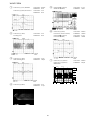
1
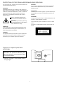
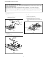
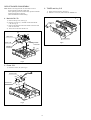
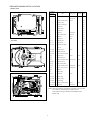
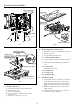
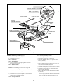
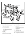
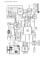
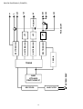
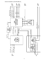
XD-DV290
K(B),EZ(B)
SERVICE MANUAL
DVD PLAYER
BASIC DVD MECHANISM : LDM-H109
(6721R-0300A)
S/M Code No. 09-99C-337-5R2
DA
TA
RE
VI
SIO
N
This Service Manual is the “Revision Publishing” and replaces “Simple Manual”
K<B>:(S/M Code No.09-99C-337-5T2)
EZ<B>:(S/M Code No.09-99C-337-5T3).
TABLE OF CONTENTS
SPECIFICATIONS .................................................................................................................................. 3
ACCESSORIES/PACKAGE LIST ........................................................................................................... 3
PROTECTION OF EYES FROM LASER BEAM DURING SERVICING/
Precaution to replace Optical block......................................................................................................... 4
DISASSEMBLY INSTRUCTIONS ...................................................................................................... 5-10
ELECTRICAL MAIN PARTS LIST ........................................................................................................ 11
TRANSISTOR ILLUSTRATION ............................................................................................................ 12
BLOCK DIAGRAM-1 (OVERALL) ......................................................................................................... 13
BLOCK DIAGRAM-2 (POWER) ............................................................................................................ 14
BLOCK DIAGRAM-3 (RF/DSP/SERVO) ............................................................................................... 15
BLOCK DIAGRAM-4 (AUDIO) .............................................................................................................. 16
BLOCK DIAGRAM-5 (MPEG) ............................................................................................................... 17
BLOCK DIAGRAM-6 (SYSTEM CONTROL) ........................................................................................ 18
WIRING-1 (MAIN: COMPONENT SIDE) ........................................................................................ 19, 20
WIRING-2 (MAIN: CONDUCTOR SIDE) ........................................................................................ 21, 22
SCHEMATIC DIAGRAM-1 (MAIN 1/5) ............................................................................................ 23, 24
SCHEMATIC DIAGRAM-2 (MAIN 2/5) ............................................................................................ 25, 26
SCHEMATIC DIAGRAM-3 (MAIN 3/5) ............................................................................................ 27, 28
SCHEMATIC DIAGRAM-4 (MAIN 4/5) ............................................................................................ 29, 30
SCHEMATIC DIAGRAM-5 (MAIN 5/5) ............................................................................................ 31, 32
SCHEMATIC DIAGRAM-6 (JACK) ................................................................................................. 33, 34
WIRING-3 (JUNCTION/JACK) ........................................................................................................ 35, 36
SCHEMATIC DIAGRAM-7 (JUNCTION) ........................................................................................ 37, 38
WIRING-4 (TIMER/KEY/POWER) .................................................................................................. 39, 40
SCHEMATIC DIAGRAM-8 (TIMER/KEY) ....................................................................................... 41, 42
SCHEMATIC DIAGRAM-9 (POWER) ............................................................................................. 43, 44
WAVE FORM ................................................................................................................................... 45-47
TROUBLE-SHOOTING .................................................................................................................... 48-57
LCD DISPLAY ....................................................................................................................................... 58
IC DESCRIPTION ............................................................................................................................ 59-77
IC BLOCK DIAGRAM ....................................................................................................................... 78-80
MECHANICAL EXPLODED VIEW 1/1 .................................................................................................. 81
MECHANICAL PARTS LIST 1/1 ........................................................................................................... 82
MECHANISM EXPLODED VIEW 1/1 ............................................................................................. 83, 84
MECHANISM PARTS LIST 1/1 ............................................................................................................. 85
2
SPECIFICATIONS
DVD VIDEO PLAYER
Power supply
Power consumption
Mass
External dimensions
Signal system
Laser
Frequency range (digital audio)
Signal-to-noise ratio (digital audio)
Audio dynamic range (digital audio)
Harmonic distortion(digital audio)
Wow and flutter
Operating conditions
100V~240V, 50Hz
20 W
3.5kg(7.7lbs)
430 * 91 * 293 (W * H * D)
NTSC
SSemiconductor laser, wavelength 655nm (DVD) /795nm (CD)
2Hz to 44kHz
More than 105dB (EIAJ)
More than 95dB (EIAJ)
0.003%
Below measurable level (less than +0.001% (W.PEAK) (EIAJ)
Temperature : 5˚C(41˚F) to 35˚C(95˚F),
Operation status : Horizontal
OUTPUTS
Video outputs
S video outputs
Component video output
Audio output (digital audio)
Audio output (optical audio)
Audio output (analog audio)
•
•
1.0V (p-p), 75Ω, negative sync., RCA jack x 1
(Y) 1.0V (p-p), 75Ω, negative sync., Mini DIN 4-pin * 1
(C) 0.286V (p-p), 75Ω
(Y) 1.0V (p-p), 75Ω,negative sync., RCA jack * 1
(Pb)/(Pr) 0.7V (p-p), 75Ω
0.5V(p-p), 75Ω, RCA jack * 1
Optical connector * 1
2.0Vrms (1kHz, 0dB), 330Ω, RCA jack (L, R) * 2
Design and specifications are subject to change without notice .
Weight and dimensions shown are approximate.
ACCESSORIES/PACKAGE LIST
REF. NO
1
2
3
4
5
PART NO.
S8-35R-S00-09G
S8-615-20G-000
S7-11R-2N0-13A
S5-640-17B-000
S5-640-18B-000
KANRI
NO.
DESCRIPTION
INSTRUCTION ASSY
DVD-2520N CABLE ASSY
REMOTE CONTROLLER A
PLUG ASSY PHONE CORD 1WAY
PLUG ASSY PHONO CORD
3
PROTECTION OF EYES FROM LASER BEAM DURING SERVICING
This set employs laser. Therefore, be sure to follow carefully the
instructions below when servicing.
CAUTION
Use of controls or adjustments or performance of procedures
other than those specified herein may result in hazardous
radiation exposure.
WARNING!
WHEN SERVICING, DO NOT APPROACH THE LASER EXIT
WITH THE EYE TOO CLOSELY. IN CASE IT IS NECESSARY TO
CONFIRM LASER BEAM EMISSION. BE SURE TO OBSERVE
FROM A DISTANCE OF MORE THAN 30cm FROM THE
SURFACE OF THE OBJECTIVE LENS ON THE OPTICAL
PICK-UP BLOCK.
ATTENTION
L'utilisation de commandes, réglages ou procédures autres que
ceux spécifiés peut entraîner une dangereuse exposition aux
radiations.
ADVARSEL!
Caution: Invisible laser radiation when
open and interlocks defeated avoid exposure to beam.
Advarsel:Usynling laserståling ved åbning,
når sikkerhedsafbrydere er ude af funktion.
Undgå udsættelse for stråling.
Usynlig laserståling ved åbning, når sikkerhedsafbrydereer ude
af funktion. Undgå udsættelse for stråling.
This Compact Disc player is classified as a CLASS 1 LASER
product.
The CLASS 1 LASER PRODUCT label is located on the rear
exterior.
VAROITUS!
Laiteen Käyttäminen muulla kuin tässä käyttöohjeessa mainitulla tavalla saattaa altistaa käyt-täjän turvallisuusluokan 1 ylittävälle näkymättömälle lasersäteilylle.
CLASS 1
KLASSE 1
LUOKAN 1
KLASS 1
VARNING!
LASER PRODUCT
LASER PRODUKT
LASER LAITE
LASER APPARAT
Om apparaten används på annat sätt än vad som specificeras i
denna bruksanvising, kan användaren utsättas för osynling
laserstrålning, som överskrider gränsen för laserklass 1.
Precaution to replace Optical block
(LPC-512A)
Body or clothes electrostatic potential could ruin
laser diode in the optical block. Be sure ground
body and workbench, and use care the clothes
do not touch the diode.
Solder
1) After the connection, remove solder shown in
the right figure.
4
DISASSEMBLY INSTRUCTIONS
CAUTION BEFORE STARTING SERVICING
Electronic parts are susceptible to static electricity and may easily damaged, so do not forget to take a proper
grounding treatment as required.
Many screws are used inside the unit. To prevent missing, dropping, etc. of the screws, always use a
magnetized screw driver in servicing. Several kinds of screws are used and some of them need special
cautions. That is, take care of the tapping screws securing molded parts and fine pitch screws used to secure
metal parts. If they are used improperly, the screw holes will be easily damaged and the parts can not be
fixed.
CABINET DISASSEMBLY
1. Top Case
3. Front Panel
1) Release 7 screws (A). (See Fig-1)
2) Lift the top case with holding the back of it, and remove
it in the direction of the arrow.
Top Case
(A)
(A)
1)
2)
3)
4)
Eject the disc tray. (See Fig-2)
Remove the tray door. (See Fig-2)
Release 2 screws (B).
Pull the front panel toward you while pressing 7
stoppers to disengage, and remove the front panel. (See
Fig-3)
(A)
(A)
(A)
(A)
(A)
(B)
Stopper
(B)
Stopper
Front Panel
Fig-1
Fig-3
2. Tray Door
1) Eject the disc tray.
2) Lift up the tray door in the direction of the arrow.
Tray Door
Disc Tray
Fig-2
5
CIRCUIT BOARD DISASSEMBLY
Note: Before removing the main circuit board, be sure to
shortcircuit the laserdiode output land.
After replacing the main circuit board, open the land after
inserting the flexible connector.
(Refer to Mechanism Disassembly)
6. TIMER and Key C.B
1) Remove the front panel. (See Fig-3)
2) Release 5 screws (E), and remove the TIMER C.B.
4. Main/JACK C.B
1) Remove the top case. (See Fig-1)
2) Release 10 screws (C), and take out the main/JACK
C.B. (See Fig-4)
3) Remove the flexible connectors and the connector from
main circuit board.
4) Then, remove the main JACK C.B.
Key C.B
(E)
(E)
(E)
(E)
(C)
(E)
(C)
JACK C.B
(C)
(C)
TIMER C.B
Main C.B
Flexible
connector
(C)
Flexible
connector
Fig-6
(C)
(C) (C)
(C)
Fig-4
5. Power C.B
1) Release 4 screws (D). (See Fig-5)
Power Code
(D)
(D)
(D)
(D)
Power C.B
Fig-5
6
DECK MECHANISM PARTS LOCATION
• Bottom View
Procedure
Parts
Starting No.
1
Junction P.C.Board
Fixing Type
4 Screws,
Disassembly Figure
Bottom
4-1
4 Locking Tabs
• Top View
2 Screws
2
Bracket Assembly Clamp
3
Bracket Clamp
4-2
4-2
4
Clamp Assembly Disk
4-2
5
Plate Clamp
4-2
5
6
Magnet Clamp
4-2
5, 6
7
Clamp Lower
2
8
Tray Disk
1 Locking Tab
4-3
2, 8
9
Base Assembly Feed
1 Connector
4-4
2, 8
10
Rubber R
1 Screw
4-4
2, 8
11
Spring Skew
1 Hook
4-4
2, 8, 11
12
Shaft PU Main
4-4
2, 8, 11
13
Shaft PU Sub
4-4
2, 8, 12, 13
14
Mechanism Assembly
4-4
2, 8, 12-14
15
Guide Freed PU
2, 8, 12-14
16
Spring Guide Feed
2, 8, 12-16
17
Pick up Assembly General
2, 8, 9
18
Motor (Mech.)
2, 8, 9
19
Shaft Lead Screw
2, 8, 9
20
Motor Assembly PU Freed 2 Locking Tabs
2, 8, 9-20
21
Base PU (Outsert)
1, 2, 8, 9
22
Base Assembly Main
1, 2, 8, 9
23
Holder Assembly Deck on 1 Locking Tab
2, 8, 9
24
Frame Assembly Up/Down
2, 8, 9
25
Rubber F
4-5
2, 8
26
Belt Loading
4-5
2, 8, 26
27
GearPulley
2, 8, 26, 27
28
Gear Loading
4-5
2, 8, 26-28
29
Gear Emergency
4-5
2, 8, 26-29
30
Cam Loading
4-2
PU Unit
1, 2, 8, 26-30 31
Motor Assembly Loading
1, 2, 8, 26-31 32 Base Main
4-4
1Screw
4-4
4-4
3Screws
Bottom
4-4
4-4
Bottom
4-4
4-4
4-5
Bottom
4-5
4-5
2 Locking Tabs
4-5
1 Screw
4-5
2 Screws
1 Locking Tab
Bottom
4-5
4-5
Note: When reassembling, perform the procedure in reverse order.
The “Bottom” on Disassembly column of above
Table indicates the part should be disassembled at the
Bottom side.
7
DECK MECHANISM ASSEMBLY
DECK ASSEMBLY
TRAY DISK
(B)
(L1)
(L2)
(L1)
EMERGENCY
EJECT HOLE
(L1)
(L1)
(C4)
(C3)
(C2)
(S1)
LEVER
JUNCTION
C.B
(C1)
(S1)
(S1)
(A)
(A)
(B)
(S1)
BOTTOM SIDE VIEW
Fig-7
Fig-9
8. Bracket Assembly Clamp (Fig-8)
BRACKET CLAMP
PLATE CLAMP
MAGNET CLAMP
CLAMP
ASSEMBLY DISK
1) Put the Deck Assembly on original position. (Top side)
2) Release 2 Screws (S2).
3) Lift up the Bracket Assembly Clamp.
(A)
8-1.
CLAMP LOWER
Clamp Assembly Disk
1) Place the Clamp Assembly Disk as Fig-(A).
2) Lift up the Clamp Assembly Disk in direction of arrow
(A).
3) Separate the Clamp Assembly Disk from the Bracket
Clamp.
(S2)
(S2)
(Fig-A)
8-1-1. Plate Clamp
1) Turn the Plate Clamp to counterclockwise direction and
then lift up the Plate Clamp.
BRACKET CLAMP
8-1-2. Magnet Clamp
8-1-3. Clamp Lower
8-2.
DECK ASSEMBLY
Bracket Clamp
9. Tray Disk (Fig-9)
1) Insert and push a Driver in the emergency eject hole (A)
at the front side, or put the Driver on the Lever (B) of
the Gear Emergency and pull the Lever (B) in direction
of arrow (A) so that the Tray Disk is ejected about 1520mm.
2) Pull the Tray Disk until the moving is locked by the
Locking Tab (L2).
3) Unlock the Locking tab (L2) in direction of arrow (B).
4) Separate the Tray Disk completely.
Fig-8
7. Junction C.B (Fig-7)
1)
2)
3)
4)
Put the Deck Assembly face down. (Bottom side)
Release 4 Screws (S1).
Unlock 4 Locking tabs (L1).
Lift up the Junction C.B a little to disconnect the
Connector (C1).
5) Disconnect 3 Connectors (C2, C3, C4).
8
CABLE FLEXIBLE
MOTOR ASSEMBLY PU FEED
BASE PU (OUTSERT)
SHAFT PU SUB
(A)
SHAFT PU MAIN
Fig-(A)
PICK UP
ASSEMBLY GENERAL
P.C. BOARD
(C5)
RED
BLACK
(S3)
SPRING
GUIDE FEED
GUIDE FEED PU
(S4)
RUBBER R
SPRING SKEW
(L4)
BASE PU (OUTSERT)
(A)
MOTOR
ASSEMBLY PU
FEED
(L3)
(A)
MOTOR (MECH.)
SHAFT LEAD SCREW
(S5)
(S5)
Fig-10
10. Base Assembly Feed (Fig-10)
10-5-3. Pick Up Assembly General
1) Disconnect the Connector (C5)
2) Release the Screw (S3).
10-6. Motor (mech.)
1) Release the 3 Screws (S5) at bottom side.
2) Push down the Motor (Mech.) and separate from the
Base PU (Outsert).
10-1. Rubber R
10-2. Spring Skew
10-7. Shaft Lead Screw
1) Press the (A) position of the Spring Skew and unlock
the Spring Skew locking.
1) Push the Shaft Lead Screw in direction on arrow (A) a
little and lift up the Shaft Lead Screw.
10-3. Shaft PU Main
10-4. Shaft PU SUB
10-8. Motor Assembly PU Feed.
10-5. Mechanism Assembly PU Unit
1) Unlock the Locking tab (L3) and lift up the P.C.Board.
2) Unlock two Locking Tabs (L4) and push down the
Motor Assembly PU Feed.
3) Separate the Motor Assembly PU Feed from the Base
PU (Outsert).
10-5-1. Guide Feed PU
1) Release the Screw (S4) and separate the Guide Feed PU
from the Pick up Assembly General.
Note: When reassembling, place the Motor Assembly PU
Feed as Fig-(A) and insert the Cable Flexible to the
Hole (A) of the Base PU (Outsert). (See Fig-(A))
Note: When reassembling, be careful not to change the
Shaft PU Main (Long) and the Shaft PU Sub (Short).
10-5-2. Spring Guide Feed
10-9. Motor (mech.)
9
(R2)
Fig-(B)
(R1)
FRAME ASSEMBLY UP/DOWN
RUBBER F
Fig-(D)
GEAR EMERGENCY
(S6)
(R1)
(R2)
GEAR PULLY
BASE MAIN
GEAR LOADING
CAM LOADING
(L6)
(S7)
(L7)
HOLDER
ASSEMBLY
DECK ON
(L6)
(L5)
Fig-(C)
BELT LOADING
(L5)
MOTOR ASSEMBLY LOADING
CONNECTOR(2 PIN)
(A)
Fig-(E)
BOTTOM SIDE VIEW
Fig-(A)
Fig-11
11-6. Gear Loading
11. Base Assembly Main (Fig-11)
11-1. Holder Assembly Deck On
11-7. Gear Emergency
1) Push the Locking tabs (L5) at bottom side of the Holder
Assembly Deck On in direction of arrow (A) and
separate to bottom side. (See Fig-(A))
Note: When reassembling, confirm that the Hole (A) of the
Cam Loading is aligned to the Hole (B) of the Gear
Emergency as Fig-(C).
For this alignment, place the Gear Emergency and
Cam Loading as Fig-(D), and then move the Gear
Emergency in direction of arrow (B) until these two
gears are aligned as Fig-(C).
11-2. Frame Assembly Up/Down.
1) Push the two Locking tabs (L6) and lift up the Frame
Assembly Up/Down.
Note: When reassembling, insert the Lever (R1) of the
Frame Assembly Up/Down to the Groove (R2) of the
Gear Emergency and lock the two Locking Tabs
(L6). (See Fig-(B))
11-8. Cam Loading
11-9. Motor Assembly Loading
1) Release two Screws (S7).
2) Unlock the Locking tab (L7) and separate the Motor
Assembly Loading to bottom side.
11-3. Rubber F
11-4. Belt Loading
11-5. Gear Pulley
Note: When reassembling, confirm that the Connector (2
Pin) is aligned as Fig-(E)
1) Release the Screw (S6) and lift up the Gear Pulley.
11-10. Base Main
10
ELECTRICAL MAIN PARTS LIST
REF. NO
PART NO.
KANRI
NO.
DESCRIPTION
REF. NO
IC
SI-AM2-980-01A
SI-AL2-402-10E
SI-AL4-981-92B
SI-RH5-983-20A
SI-RH6-859-20A
IC,AM29F800B-120EC
IC,AT24C02N-10SC-2.7
IC,AT49F8192A-90TC
IC,BA5983FP-E2
IC,BA6859AFP-E2
SI-RW8-610-00A
SI-HY2-580-10A
SI-GS7-142-60E
SI-HI6-417-03B
SI-SS4-310-00A
IC,BT861
IC,GDC25D801AA
IC,GM71C4260CJ-60
IC,HD6417034AFI20
IC,KA431AZ
SI-SS7-542-00A
SI-SS7-808-00H
SI-KE3-930-00G
SI-KE4-310-00A
87-001-196-010
IC,KA7542Z
IC,KA78R08 4P
IC,KIA393F-EL
IC,KIA431 3P
IC,KIA7042P
SI-SS4-161-02F
SI-SA8-661-12C
SI-JR3-414-00C
SI-JR4-580-00B
SI-BB1-716-00A
IC,KM4161020CT-G7
IC,LC866112B-5N21
IC,NJM3414AM-TE1,3K/REEL
IC,NJM4580M
IC,PCM1716E 28P
SI-BB1-700-00A
SI-SH2-050-00A
SI-SH3-130-00A
SI-TI7-437-40K
SI-SK6-153-00A
IC,PLL1700E 20P
IC,PQ20WZ5U 20WZ51
IC,PQ3DZ13U
IC,SN74AHC374PWLE
IC,STR-G6153T 5P
SI-TO1-254-00B
SI-TO1-254-00A
SI-TO7-040-00F
SI-MQ5-316-25A
SI-CU3-000-00A
IC,TA1254AF
IC,TA1254F
IC,TC7W04FU
IC,V53C16256HK50
IC,ZIVA3-PE0
SI-GS7-216-16C
ICGM72V161621ET-7
PART NO.
C204
C207
C213
C214
C215
KANRI
DESCRIPTION
NO.
SC-H71-06C-611
C-CAP,10UF-6.3V
SC-H71-06C-611
C-CAP,10UF-6.3V
SC-H71-06C-611
C-CAP,10UF-6.3V
SC-H71-06C-611
C-CAP,10UF-6.3V
SC-H71-06C-611
C-CAP,10UF-6.3V
C216
C218
C219
C220
C224
SC-H71-06C-611
SC-H71-06C-611
SC-H71-06C-611
SC-H81-07C-621
SC-H71-06C-611
C-CAP,10UF-6.3V
C-CAP,10UF-6.3V
C-CAP,10UF-6.3V
C-CAP,100UF-6.3V
C-CAP,10UF-6.3V
C226
C230
C302
C310
C311
SC-H71-06C-611
SC-H71-06C-611
SC-H81-07C-691
SC-H71-06F-621
SC-H71-06F-621
C-CAP,10UF-6.3V
C-CAP,10UF-6.3V
C-CAP,100UF-6.3V
C-CAP,10UF-16V
C-CAP,10UF-16V
C708
C709
C712
C713
C714
SC-H71-06C-611
SC-H82-27D-611
SC-H71-06C-611
SC-H71-06C-611
SC-H71-06F-621
C-CAP,10UF-6.3V
C-CAP,220UF-10V
C-CAP,10UF-6.3V
C-CAP,10UF-6.3V
C-CAP,10UF-16V
C718
CE201
CE202
CE203
CE205
SC-H71-06C-611
SC-H84-76C-611
SC-H84-76C-611
SC-H84-76C-611
SC-H84-76C-611
C-CAP,10UF-6.3V
C-CAP,47UF-6.3V
C-CAP,47UF-6.3V
C-CAP,47UF-6.3V
C-CAP,47UF-6.3V
CE206
CE210
CE211
CE221
CE223
SC-H84-76C-611
SC-H84-76C-611
SC-H84-76C-611
SC-H84-76C-611
SC-H84-76C-611
C-CAP,47UF-6.3V
C-CAP,47UF-6.3V
C-CAP,47UF-6.3V
C-CAP,47UF-6.3V
C-CAP,47UF-6.3V
CE228
CE609
CE610
CE710
X101
SC-H84-76C-611
SC-H81-07F-611
SC-H81-07F-611
SC-H84-76C-611
S2-12H-B20-02A
C-CAP,47UF-6.3V
C-CAP,100UF-16V
C-CAP,100UF-16V
C-CAP,47UF-6.3V
CCR20.0MC6T TDK 20000000H
X301
S2-02R-427-01G
C-RESO 27MHZ 20P
TRANSISTOR
ST-R10-500-9AD
ST-R10-300-9AE
ST-R10-500-9AB
ST-R11-510-0AA
ST-R12-670-9AC
TR,KRA105M
TR,KRC103M
TR,KRC105M
TR,KSB1151-Y
TR,KTA1267-GR
ST-R15-040-9BF
ST-R15-050-9AD
ST-R31-980-9AC
ST-R13-040-9BA
ST-R10-000-9CB
TR,KTA1504S-Y
TR,KTA1505S-Y
TR,KTC3198-TP-BL
TR,KTD1304S
TR,UMX1N
ST-R10-000-9BM
87-070-334-070
SM-TZ6-8CT-000
TR,UMZ1N 3K
ZENER,MTZ10B
ZENER,MTZ6.8C
JUNCTION C.B
C-DIODE,KDS193
C-TR,2SA1037K-Q
C-TR,KRC103S-T1
C-TR,KTC3875S-GR-T1
DIODE,1N5402
87-020-465-080
SD-R10-451-0AA
SD-D01-000-9CA
SD-R18-020-9AA
87-A40-284-080
DIODE,1SS133
DIODE,B10A45V1
DIODE,EG01CW
DIODE,ERA18-02KFRB
DIODE,ERA22-10
SD-D01-000-9AC
83-NEG-677-080
SD-R49-500-9AA
87-017-352-010
87-070-173-010
DIODE,EU01W
DIODE,MTZ5.6B
DIODE,RB495D
DIODE,RU3YXLF-C1 100V2
DIODE,S1WBA60
87-010-140-080
87-010-140-080
87-010-140-080
87-010-140-080
SR-D01-01H-633
CAP,E 47-16V
CAP,E 47-16V
CAP,E 47-16V
CAP,E 47-16V
RES,1-1/2W
R452
SR-D01-01H-633
RES,1-1/2W
C500
C502
C506
C507
C512
SC-E22-73D-638
SC-E10-63F-638
SC-E47-63J-638
SC-E10-63F-638
87-010-140-080
CAP,E
CAP,E
CAP,E
CAP,E
CAP,E
C513
DIG501
LED501
RC501
SW501
87-010-140-080
S3-02H-V00-1D0
SD-L32-531-9AA
S7-12R-083-8GA
S5-562-19B-000
CAP,E 47-16V
7-BT-259GK DH
LED SPR325MVWT31(GRN)
TSOP1238UQ1 TEMIC 8MM 37 RC
SW,SKHV10910B
SW502
SW503
SW503
SW504
SW505
S5-562-19B-000
S5-562-19B-000
S5-562-19B-000
S5-562-19B-000
S5-562-19B-000
SW,SKHV10910B
SW,SKHV10910B
SW,SKHV10910B
SW,SKHV10910B
SW,SKHV10910B
SW506
SW507
SW510
SW511
SW512
S5-562-19B-000
S5-562-19B-000
S5-562-19B-000
S5-562-19B-000
S5-562-19B-000
SW,SKHV10910B
SW,SKHV10910B
SW,SKHV10910B
SW,SKHV10910B
SW,SKHV10910B
SW513
S5-562-19B-000
SW,SKHV10910B
TIMER C.B
DIODE
SD-D19-300-9AB
ST-R10-370-9BB
ST-R10-300-9AA
ST-R38-750-9AC
SD-R15-402-0BA
CE450
CE451
CE452
CE453
R451
220-10V
10-16V
47UF-35V
10-16V
47-16V
MAIN C.B
11
REF. NO
SW514
X501
PART NO.
KANRI
DESCRIPTION
NO.
S5-562-19B-000
SW,SKHV10910B
S6-160-20P-000
CSA6.00MGU MURATA 6MHZ
REF. NO
JACK C.B
PART NO.
C906
C907
C913
C916
C918
KANRI
DESCRIPTION
NO.
S6-240-87B-000
CAP,100P-1KV
SA-1B3-0KH-2M0
CAP,220PF-400V
87-012-379-010
CAP,3300PF-400V
87-010-387-010
CAP,E 470UF-25V KME
87-010-112-080
CAP,E 100-16V
CV1
CV2
CV3
CV6
CV8
87-010-060-080
SC-E22-76F-638
87-010-237-910
87-015-681-080
87-010-140-080
CAP,E
CAP,E
CAP,E
CAP,E
CAP,E
100-16V
220UF-16V
1000UF-16V
10-16V
47-16V
C919
C921
C923
C924
C925
87-010-408-040
SC-E22-76F-638
87-010-237-910
87-010-237-910
87-010-375-080
CAP,E
CAP,E
CAP,E
CAP,E
CAP,E
47UF-50V
220UF-16V
1000UF-16V
1000UF-16V
330-10V
CV10
CV12
CV13
CV14
CV15
SC-E10-86F-630
87-015-681-080
87-015-684-080
87-015-681-080
87-015-681-080
CAP,E
CAP,E
CAP,E
CAP,E
CAP,E
1000-16V
10-16V
47-16V
10-16V
10-16V
C926
C927
C929
C932
C934
87-010-408-040
87-015-684-080
87-010-112-080
SC-E47-7CD-638
SC-E47-7CD-638
CAP,E
CAP,E
CAP,E
CAP,E
CAP,E
47UF-50V
47-16V
100-16V
470UF-10V
470UF-10V
CV16
CV21
JACK1
JACK2
JACK3
87-016-577-080
87-010-060-080
S6-12H-K26-02A
S5-720-75A-000
S6-12R-IH0-05D
CAP,E 470UF-16V
CAP,E 100-16V
TOTX178 TOSHIBA AN/DIP
BJP-202L BAEEN BLACK
JACK,PPJ6031J
!F901
!IC903
!L901
!L901
L902
S5-850-11T-000
S6-570-62B-000
S6-161-45H-000
S6-161-45J-000
S6-330-88G-000
FUSE,1600MA 250V
SENSOR PC123Y
FILTER SHT LFS2020V4-04350
FL BUJEON V-04350
COIL,CHOCK TP 5MM
JACK4
JACK8
S6-12R-BH0-08A
YKF51-5506 JALCO HORIZONT4P
L903
R901
R902
R911
R922
S6-330-88D-000
S6-140-07R-000
SR-S10-03K-619
SR-S05-10K-619
SR-S12-00J-619
COIL,20UH
RES,2.7-2W
RES,100K-2W
RES,0.51-2W
RES,M/F 120-1W
!T901
!V901
S6-420-23T-000
S6-560-04F-000
PT,SHT-023T/KSE-023T
SVR681D10A SAMYANG 680V
KEY C.B
SW508
S5-562-19B-000
SW,SKHV10910B
POWER C.B
C900
C901
C902
C902
C905
87-010-408-040
S6-240-88B-000
S6-240-88B-000
S6-240-88F-000
87-016-375-010
CAP,E 47UF-50V
CAP,0.1UF-250V
CAP,0.1UF-250V
CAP,PCX2 275V 0.1UF,M
CAP,0.01UF-630V
• Regarding connectors, they are not stocked as they are not the initial order items.
The connectors are available after they are supplied from connector manufacturers upon the order is received.
CHIP RESISTOR PART CODE
Chip Resistor Part Coding
8 8
A
Figure
Resistor Code
Value of resistor
Chip resistor
L
W
t
:A
Resistor Code : A
1.0
0.5
0.35
104
Dimensions (mm)
Wattage
1/16W
Type
1005
Symbol
CJ
Tolerance
5%
1/16W
1/10W
1608
2125
5%
5%
CJ
CJ
1/8W
3216
5%
CJ
Form
L
t
1.6
0.8
0.45
108
2
1.25
0.45
118
3.2
1.6
0.55
128
W
TRANSISTOR ILLUSTRATION
C2
C
B
ECB
ECB
KRA105M
KRC105M
KRC103M
KSB1151
E
BCE
2SA1037K KTC3875S
KTA1504S KTC4419
KTA1505S KTD1304S
KTC3198
12
KSE13005F
B1
E1
E2
B2
C1
UMX1N
UMZ1N
13
AC 100
~240V,
50
~60Hz
OPEN S/W
LIMIT S/W
FL DISPLAY
POWER
BOARD
focus, tracking sled
KEY INPUT
IC500
LC866112
AGND,GND,UGND
+5VU
+5VD
+5VA
+9V
-21.8V
-27V
-22.5V
Loading
spindle
PICK
UP
CLOSE S/W
M
DECK MECHANISM
M
LOADING
MOTOR
SPINDLE
MOTOR
DVD : A, B, C, D
DVD : RF
CD : A, B, E, F
REMOCON
RECEIVER
DRAM
33.8688MHz
REQZI
SDCLKI, ZISENB
DVD_DATA[0:7]
IIC_DATA,
IIC_CLK
S_CLK, S_DATA,
DPLL_L
D[00:07]
A[00:02]
DAC_L0,
S_CLK
S_DATA
IC703/IC601~603
PCM176x4
AUDIO
DAC
DA_DATA,
DA_LRCK,
DA_BCK
DA_XCK
DA_DATA,
DA_LRCK,
DA_BCK
IC306
GM72V1621
1M X 16bit
SDRAM
27MHz
X-TAL
IC308
PLL1700
CLOCK
GENERATROR
SENS, FOK, SLD_FG,
MSDAT0,DEFECT,DSP_SENSE,
SQSO, SQCK, SCOR, AO[0:5]
XLAT, S_CLK, S_DATA, DO[0:7]
IC206
DVDSP-3301
CD/DVD DSP
DVD SERVO
FLASH
MEMORY
IC108
SH7034
SPINDLE_FG, SLD_FG
RXDO/TXDO/SCKO
F_Reg/M_Reg/M_Reset/MD_SW
POWER CONTROL
IC401
BA5983
POWER
DRIVER
FDO,TDO,
FMO
MON, SPINDLE_DRV
FE, TE, RFRP, SBADD, DVD/CD RF
TEBAL, FEBAL,
DPOCTL, EQF, EQB
LOADING DRIVE
IC400
BA6859FP
SPINDLE
MOTOR
DRIVER
IC201
TA1254F
RF SIGNAL
PROCESSOR
DRAM
256K x 16bit
ICADDR[0:8]
Comp.
R
L
IC301
ZiVA-3
MPEG A/V
Decoder
DVD_SD_CS0,
DVD_UDQM
DVD_MD[0:15]
DVD_MA[0:11]
L
AUDIO
OUT
R
AMP
DVD_SD_CAS,
DVD_SD_RAS
DVD_SD_CLK
DVD_MWE
C
Y
Pr
Pb
FILTER
Component
VIDEO OUT
Y
FILTER
Composite, Y, C
IC800/IC801
BT865A/861A
NTSC/PAL
Encoder
27MHz
ICDATA[00:15]
DVD_LDQM, DVD_SD_CS1
VDATA[0:7]
IC307
GM72V1621
1M x 16bit
SDRAM
Vsync
RFRP, RFCen,
TE, Vref
Hsync
Composite
DISC
BLOCK DIAGRAM-1 (OVERALL)
Q901
KTC4419
SWITCHING IC
RECTIFIER
14
AC100V~240V
FEED B.
LPF
LPF
RECTIFIER(5.2V)
LPF
RECTIFIER(10V)
RECTIFIER(14V)
RECTIFIER(FLD)
PWR ON/OFF
REG(8V)
U5V
A5V
D5V
8V
12V
-24V
F-
F+
BLOCK DIAGRAM-2 (POWER)
TRANS
LINE FILTER
M/D
PICK
UP
spindle
4
15
focus, tracking, loading, sled
IC400
BA6859AFP
Spindle
Motor Driver
CD : A, B, E,F
DVD : RF
4
IC401
BA5983
Power Driver
IC201
TA1254AF
RF Signal
Processor
FDO, TDO, FMO
IC206
GDC25D801AA
CD/DVD DSP
IC205
DRAM
256K x 16bit
loading drive
SPINDLE_FG, SLD_FG
TEBAL, FEBAL,
DPOCTL, EQF, EQB
MON, SPINDLE_DRV
5
DVD/CD RF
FE,TE,RFRP,SBADD 4
RFZ_HOLD
MIRR,TZC
ICADDR[0:8]
9
DVD : A,B,C,D
2
16
IC204
comp.
ICDATA[00:15]
RFRP, RFCen,
4
TE, Vref
ZO[0:7]
8
MCK
AO[0:5]
4
XLAT,S_CLK, S_DATA
3
DO[0:7]
SQSO, SQCK, SCOR
3
8
SENS, FOK, SLD_FG,
MSDATO, DEFECT, DSP_SENSE
5
UCOM
I/F
MPEG
I/F
MPEG
I/F
UCOM
I/F
UCOM
I/F
BLOCK DIAGRAM-3 (RF/DSP/SERVO)
MPEG I/F
(IC301)
µ-com I/F
(IC108)
16
DA_DATA0
DA_XCK
DA_BCK
DA_LRCK
DAC_L0
S_CLK
S_DATA
MPEG_RST
CH 1/2 : DOWNMIX Lt / Rt
IC703
PCM1716
Audio DAC
R0
L0
IC704
LPF &
Buffer
NJM4580M
OP AMP
Rt
Lt
TO
JACK BOARD
BLOCK DIAGRAM-4 (AUDIO)
17
18
FRONT
I/F
MICOM_RESET
2
2
A[19:21]
D[00:04]
/IOCSI, /WR 2
SENS_MCOM,
MICOM_WAIT
2
A[01:19]
IC114
EEPROM
AT24C02
2
16
D[00:15]
A[01:21] 21
16
8
2
9
16
D[00:15]
IC107
DRAM
256K x 16
A[01:09]
D[00:15]
EXP_W2,
/PWR_CLT
D[00:07]
8
D[00:07], A[00:05], E_SIN, E_CLK
LOAD FR, F/R, LOCK, DEFECT, FOK,
DSP_SENSE
2
IC102
74HC374
8
MPEG_CTL,
E_DR,
/ZOOM_RST,
/S_XRST,
XLAT,
ACT_MUTE,
V_MUTE,
A_MUTE
DSP
I/F
SERVO
I/F
MCK
VIDEO
I/F(A/V)
UCOM
I/F
SERVO
I/F
Y/C
COMPOSITE1
Pr
Pb
Y
AUDIO
I/F(A/V)
S_CLK, S_DATA, DPLL_L
IC801
BT861A
NTSC/PAL
Encoder
BCA_CODE SPINDLE_FG, SLD_FG,
27MHz
X-TAL
IC308
PLL1700
CLOCK
GENERATROR
MPEG_CLK
DA_XCK
VDATA[0:7]
HSYNC, VSYNC
SPDIF
DA_BCK
DA_DATA[0:3]
IC108
SH7034
MAIN µ-COM
2
IC106
FLASH
MEMORY
512K x 16
19
4
DVD_LDOM,
DVD_SD_CSI
IIC_CLK,
IIC_DATA
D[00:07], A[00:02], IIC_CLK, IIC_DATA, SCLK0,
MPEG_INT
IC101
XC9536
EXPANDER
PWR_CTL,
SENS, LIMIT_SW,
MIC_ON, CLOSE_SW,
OPEN_SW, MPEG_WAIT,
ZIERR
8
12
IC307
GM72V1621
1M x 16bit
SDRAM
16
IC301
ZiVA-3
MPEG A/V
Decoder
ECHO, MIC_A, DISC_A, S_DATA, S/CLK
4
DVD_SD_CAS
DVD_SD_RAS
DVD_SD_CLK
DVD_MWE
DVD_MA[0:11]
DVD_MD[0:15]
IC306
GM72V1621
1M x 16bit
SDRAM
MPEG_ERROR,
DAC_L0,
RF_LAT,
/DSP_CS,
/MPEG_CS,
/PP_CS
6
2
8
3
2
8
DVD_SD_CS0, DVD_UDOM 2
IIC_DATA, IIC_CLK
MPEG_ERROR
D[00:07]
A[00:02]
REQZ1
SDCLK1,ZISENB
MPEG
I/F
A/V
I/F
µ-COM
I/F
DSP
I/F
DVD_DATA[0:7]
BLOCK DIAGRAM-5 (MPEG)
BLOCK DIAGRAM-6 (SYSTEM CONTROL)
WIRING-1 (MAIN: COMPONENT SIDE)
14
13
12
11
10
9
8
6
7
4
5
3
2
1
A
MAIN C.B
(COMPONENT SIDE)
TO/FROM
POWER C.B
CON902
TO/FROM
JUNCTION C.B
CN402
TO/FROM
JUNCTION C.B
CN404
B
2
20
2
19
1
1
26
10
25
1
E
E
C
64
49
48
1
1
2
TO/FROM JACK C.B
CON06
TO/FROM TIMER C.B
CN507
E
R801
33
16
R184
C128
14
17
15
5
1
R191
1
5
5
8
5
1
4
R787
R714
1
53
52
105
84
R726
C715
R723
R721
C713
E
57
85
56
R399
E
R364
R365
R366
112
1
105
F
2
104
TO/FROM JACK C.B
CON07
156
157
29
1
28
1
156
157
208
15
21
Cxxx
1
G
22
40
R384 208
1
R385
1
53
R307
2
22
R729
C712
14
21
R732
CE711
D
1
104
NOTE
R727
C227
2
32
52
R312
R309
H
Lxxx
Rxxx
20
21
I
C
E
B
E
J
19
20
WIRING-2 (MAIN: CONDUCTOR SIDE)
1
2
3
4
5
6
7
9
8
11
10
12
13
A
MAIN C.B
(CONDUCTOR SIDE)
B
20
11
1
10
C
D
25
24
48
1
1
E
44
50
1
50
25
26
25
26
4
1
3
8
5
1
4
40
34
1
1
6
33
11
12
23
22
3 1
4 6
1
F
4
8
8
5
1
4
C728
5
20
11
10
20
1
R188
28
15
1
14
R777
G
21
R717 CE712
R736
E
NOTE
E
Cxxx
5
R193
E
5
E
H
C202
8
1
80
E
E
E
1
E
61
60
1
4
E
Lxxx
8
5
E
20
Rxxx
1
I
21
R823
E
40
C
B
E
4
41
E
J
21
22
E
14
SCHEMATIC DIAGRAM-1 (MAIN 1/5)
23
24
SCHEMATIC DIAGRAM-2 (MAIN 2/5)
25
26
SCHEMATIC DIAGRAM-3 (MAIN 3/5)
27
28
SCHEMATIC DIAGRAM-4 (MAIN 4/5)
29
30
SCHEMATIC DIAGRAM-5 (MAIN 5/5)
31
32
AA+12V
SCART1 (16:9)
SCART2 (DVD/AV)
COMPO1
L1
R1
U (B)
V (G)
SCHEMATIC DIAGRAM-6 (JACK)
QV01
KTA1267
CV16
470µF
/16V
RV31
180
QV03
KRC103M
RV32
680
RV03
10K
QV07
KTA1267
RV33
75
DV02
1SS133
RV08
820
QV02
KRC103M
RV04
2.2K
RV05
1.0K
CV12
10µF
CV24
220µF
/16V
JK08
SCART JACK
JACK08
EURO AV (TV)
A Rout
FV06
A Lout
GND
GND
BVD01
BEAD
BLUE
CONTROL
FV07
BVD02
BEAD
GREEN
FV08
GND
GND
RED
BVD03
BEAD
GND
GND
V.–out
FV05
LV01
1µH
GND
33
34
WIRING-3 (JUNCTION/JACK)
1
2
3
4
5
6
7
8
9
A
JACK03
JACK04
AUDIO OUT
S-VIDEO
OUT
12
1
VIDEO
OUT
1
C
D
E
JUNCTION C.B
TO/FROM
MAIN C.B
CON202
SW1
M1
INSIDE
LIMIT
SW
SPINDLE
MOTOR
M
TO/FROM
MAIN C.B
CON201
TO/FROM
MAIN C.B
CON201
TO/FROM
MAIN C.B
CON801
M2
(SLED MOTOR)
M3
(LOADING MOTOR)
M
M
F
G
H
NOTE
I
OPEN/CLOSE
SWITCH
E
J
PICK UP
ASSY
C
B
TO/FROM
POWER C.B
CON904
K
35
14
JACK08
EURO AV (TV)
R
JACK C.B
3
13
L
DIGITAL OUT
JACK01
JACK02
OPTICAL COAXIAL
B
11
10
36
5
10
15
20
SCHEMATIC DIAGRAM-7 (JUNCTION)
37
38
WIRING-4 (TIMER/KEY/POWER)
1
2
3
4
5
6
7
8
9
10
11
12
A
B
C
D
E
F
G
H
I
J
K
39
40
13
14
SCHEMATIC DIAGRAM-8 (TIMER/KEY)
41
42
SCHEMATIC DIAGRAM-9 (POWER)
POWER C.B
C932
470µ/10V
A5V REG.
4
1
3
2
INSULATOR
POWER
CONTROL
AC 200-240V
50Hz
43
44
TO TIMER C.B
CN503
+8V REG.
TO JUNCTION C.B
CN401
TO MAIN C.B
CON999
T901
WAVE FORM
1
IC201 Pin ( (LVL) SBADD
IC201 Pin ¡ (FEO) Focus Error
2
3
VOLT/DIV:
TIME/DIV:
VOLT/DIV:
TIME/DIV:
5
500mV
2mS
2.9V
2mS
6
IC201 Pin ) (TEO)
Tracking Error
VOLT/DIV: 2.2V
TIME/DIV: 2mS
IC201 Pin ) (TEO)
VBR Tracking Error
VOLT/DIV: 2.27V
TIME/DIV: 500µS
7
IC206 Pin 88 (A OUT3)
SLED Drive (FMO)
VOLT/DIV: 2.12V
TIME/DIV: 10mS
IC201 Pin ¡ (FEO)
Focus Error (In Focus search)
IC206 Pin 83 (A OUT1)
Focus Drive (FDO)
VOLT/DIV:
TIME/DIV:
VOLT/DIV:
TIME/DIV:
IC801 Pin #-^ (P0-P3)
IC801 Pin (-™ (P4-P7)
MPEG Data
VOLT/DIV: 280mV
TIME/DIV: 500µS
Tek Stop : 1 00kS/s
[
3290 Acqs
T
]
Record
Length
Fit to Screen
OFF
500
points in
10divs
T
1000
points in
20divs
2500
points in
50divs
3
Ch3
4
Time Base
Main
IC201 Pin • (RFO)
VOLT/DIV: 0.5V
TIME/DIV: 0.1µS
45
M 500µs
1.00V
Trigger
Position
50%
Record
Length
2500
Horiz
Scale
(/div)
CH1
Horiz
Pos
280/mV
FastFrame
Setup
more
1 of 3
200mV
100mS
2.14V
100mS
8
IC801 Pin 57 (DACC)
Composite
@
VOLT/DIV: 500mV
TIME/DIV: 20µS
IC801 Pin 71 (CLK IN)
MPEG Clock
Tek Stop : 1 00kS/s
[
3290 Acqs
T
VOLT/DIV: 280mV
TIME/DIV: 500µS
]
Edge Slope
T
3
Ch3
Source
Ch1
Type
<Edge>
9
IC801 Pin 58 (DACB)
Chrominance
#
VOLT/DIV: 500mV
TIME/DIV: 20µS
M 500µs
1.00V
Coupling
DC
CH1
Slope
280/mV
Level
280mV
IC801 Pin ≤ (VSYNC)
Vertical SYNC
Tek Stop : 10.0kS/s
[
13 Acqs
T
Mode
&
Holdoff
VOLT/DIV: 280mV
TIME/DIV: 5mS
]
Edge Slope
T
3
Ch3
Source
Ch1
Type
<Edge>
$
0
IC801 Pin
Luminance
59
(DACA)
VOLT/DIV: 500mV
TIME/DIV: 20µS
M 5 .00ms CH1
1.00V
Coupling
DC
Slope
280/mV
Level
280mV
IC801 Pin ∞ (HSYNC)
Tek Stop : 2.50MS/s
[
7 Acqs
T
Mode
&
Holdoff
VOLT/DIV: 280mV
TIME/DIV: 20µS
]
Edge Slope
Tek Stop : 2.50MS/s
4 Acqs
[T
]
T
T
3
M 20.0µs
Ch3
3
Type
<Edge>
M20.0µs
Ch3
!
500mV
IC801 Pin
IC801 Pin
SDA/SCL
75
76
(SID)
(SIC)
Glitch Ch1
2 Apr 1999
14:47:27
%
VOLT/DIV: 2.06V
TIME/DIV: 25mS
46
1.00V
Source
Ch1
Coupling
DC
IC801 Pin + (DACF)
Component Pb
CH1
Slope
280/mV
Level
280mV
Mode
&
Holdoff
VOLT/DIV: 500mV
TIME/DIV: 20µS
^
&
IC801 Pin , (DACE)
Component Pr
VOLT/DIV: 500mV
TIME/DIV: 20µS
IC801 Pin < (DACA)
Component Y
VOLT/DIV: 500mV
TIME/DIV: 20µS
47
TROUBLE-SHOOTING
1. Power Circuit
•
•
•
•
Input Voltage: 120V
It is possible to malfunction, if the unload condition is left for a long time when power is on.
(More than Dummy load 100mA)
A Primary side is abnormal when the fuse is short, secondary side is abnormal when the IC103 oscillates intermittently.
The resistor value of both terminal is measured with DVM crossing each other to check the each element is normal or abnormal.
(It is normal when the numerical value is different each other.)
START
Is F901 normal?
A primary side is abnormal.
Check the GND of C901 and
IC901 Pin 3 with oscilloscope.
NO
Is IC901 Pin 3
Is IC905
switching normally?
normal?
<Fig-3-1>
YES
YES In condition of DC140V.
(Feedback is abnormal)
When IC901
oscillating
NO
Is CN903 Pin 3 5.2V?
Are D908, D909,
D907, D910, D906
and D905 normal?
YES
Replace Q908
and Q909.
NO Is CON903 Pin 3
5.2V?
YES
NO
Replace
IC902.
NO
Check Q904
and ZD903.
Replace
defective
parts.
NO
NO
YES
Check or
replace
D908.
Are D901, R904,
R905 and R906
normal?
NO
YES
After connect
CON903
Pin 1, 3 short.
Are R922, C927, R921 NO
and R918 normal?
NO
Is PC901 normal?
YES
(A)
NO
Are R907, D902,
D903 and R902
normal?
YES
Board is
abnormal
Is voltage of
BD901 140V?
YES
YES
NO
Does oscillate
continuously when
the CON903 is
disconnected ?
YES Secondary side
is abnormal.
Front Circuit
NO
END
Are CON902
Pin 5, 6 and
9 5V?
YES
Replace defective
parts.
Is CON904
Pin 3 8V?
YES
Is CON902
Pin 3 12V?
YES
To (A).
Are CON903
Pin 5 -24V, Pin 7 -20V and
Pin 8 -16V?
NO
YES
IC901 Pin 3
Normal switching waveform on the
stand-by mode at the AC110V
END
48
2. µ-COM Circuit
A. No Power
POWER ON
Power RED LED on?
NO
Refer to Front Part.
YES
Does Bar appear
at FLD?
YES
NO
Do all five Bars
appear?
NO
Does Logo appear
on the screen?
NO
Is CON107
connected normally?
YES
Reconnect it.
Check power.
(Refer to power)
NO
If power is
normal
YES
OK
NO
Is CON107 Pin 6
normal?
Refer to Front Part
1
YES
1
A
Is oscillation of
X101 normal?
NO
NO
Check the oscillation
The
waveform on A [00:21]
and D [00:15] of IC108
normal?
YES
YES
Check short
Are IC107 Pin $, •
and ª normal?
NO
NO
Check short.
Are IC101
Pin 7, 8 normal?
OK
YES
A
YES
Replace IC101.
Replace IC107
or IC108.
Replace Main B/D.
END
49
B. Audio abnormal
C. Video abnormal
AUDIO ABNORMAL
VIDEO ABNORMAL
Check Audio jack.
Check Video jack.
YES (If OK)
YES (If OK)
Check PLL FC of
MPEG part.
Refer to Video part.
YES (If OK)
YES (If OK)
Refer to Encoder part.
Refer to Audio part.
YES (If OK)
YES (If OK)
Refer to MPEG part.
Refer to MPEG part.
YES (If OK)
YES (If OK)
Replace B/D.
Replace B/D.
END
END
D. Open/Close abnormal
OPEN/CLOSE ABNORMAL
Check Front.
YES (If OK)
Check the
connection of
CON107.
YES
NO
Check the connection of MD.
YES
Check IC101
Pin #, $.
YES
Refer to SERVO part.
50
NO
Reconnect it.
E. Picture abnormal
PICTURE ABNORMAL
Check the disc.
Refer to Servo part
If OK
Check PLL IC of MPEG part
YES (If OK)
Check DSP
YES (If OK)
Check MPEG
YES (If OK)
Replace B/D
END
F. Disc Error
DISC ERROR
Check Disc
YES (If OK)
Refer to Servo part
YES (If OK)
Replace B/D
END
51
3. MPEG Circuit
Power is on
Does aiwa Logo appear
on the screen?
NO
Check power & clock.
A
YES
YES
Does the
moving picture of the DVD Disc
play on the screen
normally?
NO
Is MPEG data
signal normal?
YES
YES
YES
Is error signal normal?
NO
OK
NO
Check CD/DVD DSP
output signal.
B
OK
Check MPEG Decoder
input signal.
C
Check CD/DVD DSP
output signal.
D
OK
Does the
moving picture of the video
CD play on the screen
normally?
NO
Is MPEG data
signal normal?
NO
I OPTION
If included VCD function.
Is Clock normal?
E
Check CD/DVD DSP
output signal.
F
OK
YES
YES
Check MPEG Decoder
input signal.
Check MPEG Decoder
input signal.
G
Check clock signal
H
Check clock signal
I
NO
YES
Does the
audio sound output
normally?
YES
NO
Does the audio
sound output from MPEG
decoder?
YES
END
52
4. Front Circuit (Digitron & key)
START
Power on.
NO
LED ON?
NO
Is oscillation of
X501 normal?
YES
Check Power.
YES
Is Digitron on
normally?
NO
YES
CD
Do all
the buttons work
normally?
NO
Check waveform
of IC500 Pin 6.
Replace IC501.
YES
NO
Is waveform of IC500
Pin 76 normal?
YES
NO
Check waveform
of IC500 Pin #.
YES
YES
Check waveform of
IC500 Pin #.
NO
NO
Solder Key part.
Replace IC500.
YES
Solder defective parts again
Check waveform
of Q500 Pin 2.
YES
Check and replace R516,
R507, R506, R500, R505,
R504, R512 and R503.
Does remote control
work normally?
YES
NO
Replace Q500.
Replace LED501.
Does pulse
waveform of RE500
Pin 3 appear?
NO
YES
Is RE500 Pin 2
5V?
NO
Solder defective parts
YES
Is IC500
Pin ≤ connected to
RE500 Pin 3?
Replace RE500
YES
YES
Complete repairing
Front B/D.
NO
Re-solder.
Replace IC500.
YES
YES
53
Recheck
5. RF/Servo Circuit
A.
CHECK POINT (General)
Does signal goes
“High” to IC206 Pin 194 when
the power is on?
NO
YES
Does signal
pulse input to IC206 Pin
when the power
is on?
58
,
59
NO
Check “2.µ-COM Part”.
YES
Does TTL
pulse output to IC206
Pin 140 , 142 ?
NO
Does
33.8688MHz clock input
to IC206 Pin 63 ?
YES
YES
Replace IC206
(IC206 soldering or IC defect).
Is IC206
Pin
83, 84 , 88 , 89
voltage
about 2.2V?
NO
Replace IC700
(IC700 soldering or IC defect).
YES
END
54
NO
Replace X301 or IC308
(30MHz clock defect)
B.
No disc
Power on
Does tray open
or close?
Check loading Part.
NO
Push Pick-up to inner track
to the end by hand.
YES
Does
CON202 Pin & change
high to low?
NO
DECK assembly is defective.
(Limit sw)
NO
check µ-COM Part.
YES
Pressing
the open/close key repeatedly,
check the voltage of CON202 Pin 9
change 0V to 5V
YES
Junction Board
Does
the voltage change at
IC401 Pin %, ^ more than 2V on the
basis of 4.5V?
NO
Replace IC401.
YES
Fig-1. SLED Driver waveform
Does the pick-up
slide inner or outer
track?
YES
NO
DECK assembly is defective.
Check SLED Driver output.
IC206 Pin 88 IC401 Pins *, &.
IC206 Pin 88 no output : IC206 is defective
IC401 Pin * no output : IC401 is defective
Fig-2. Focus Driver waveform
Does
the pick-up lens move up
and down?
NO
Check Focus Driver output.
IC206 Pin 83 no output : IC700 is defective
(IC206 Pin 83 , IC401 Pins !, @) IC401 Pin 1, 2 no output : IC701 is defective
YES
Slide the pick-up to
inner track.
END
55
C.
DISC IN
OPEN/CLOSE
Fig-3. FOCUS ERROR waveform
NO
FOCUS ON?
Check
the focus error moving the
lens up and down. (IC201
Pin ¡)
NO
52 , 53 , 54 , 55
58 , 59 , 60 , 61
in DVD Mode
in CD Mode
IC201 no output: Pick-up is defective.
YES
YES
Check IC201 Pin
Check IC201 Pin
Does the
TTL level change at IC206
Pin 78 and 132 moving
the lens?
NO
Replace IC206.
YES
Replace µ-COM or IC206.
NO
Does the disc turn?
Check CON404 Pin 4, 6
Motor turn when the Pin 4 is
less than 1.6V
Check IC206 and IC403 when the Pin 4 is abnormal
YES
NO
IC206 Pin 169 is “High”?
Check A
YES
NO
Does the signal
pulse input at IC700 Pin ≥,
• and ª?
Is OK the track jump.
YES
YES
NO
Does the screen appear?
Video Par is defective.
Check “5.MPEG Circuit.”
Check “7.OSD/Video Circuit.”
YES
END
56
Replace IC700.
NO
µ-COM part is
defective. Check
“2.µ-COM Circuit.”
D.
CHECK A
Fig-5. RF
waveform
NO
Check RF Eye-Pattern.
RF: 1.0-2.1V (IC201 Pin •)
Check IC201 Pin
Check IC201 Pin
52 , 53 , 54 , 55
58 , 59 , 60 , 61
in DVD Mode.
in CD Mode.
No signal: Pick-up is defective
YES
NO
Is the eye-pattern vivid?
YES
Does the
sawtooth waveform emit
at IC201 Pin )?
NO
Does the 1.6V emit?
NO
YES
YES
Replace IC206.
Check IC206 Pin
84 .
No signal at IC206: IC206 is defective
• Check IC206 Pin 162
• Check the clock at the IC206
Pin •, º.
• Both are normal: IC206 is defective
END
57
Replace IC201.
LCD DISPLAY
58
IC DESCRIPTION
IC, BT861
Pin No.
Pin Name
I/O
Description
Secondary video input port. Pixel data (TTL compatible) in 8-bit YCrCb format. A
1-6
VID2-7
I
higher index corresponds to a greater bit significance. Data on the VID port is latched
by rising edge of VIDCLK. (Connected to GND.)
7
VDD
—
Digital power.
8
GND
—
Digital ground.
9
VIDCLK
I
2x pixel clock for secondary video input port. Synchronization circuitry exists for this
port to lock it to the primary video port. (Connected to GND.)
Video data valid qualifier. A logical 1 indicates data on VID [7:0] is valid data. The
10
VIDVALID
I
sense of this signal is controlled by the VIDVALIDI bit of register 0x1C. (Connected
to GND.)
11
VIDVACT
I
Vertical active display region. The sense of this signal is controlled by the VIDVACTI
bit of register 0x1C. (Connected to GND.)
Horizontal active pixel signal. A logical 1 indicates data on VID [7:0] is in the
12
VIDHACT
I
horizontal display region. The sense of this signal is controlled by the VIDHACTI bit
of register 0x1C. (Connected to GND.)
Primary video input port. TTL compatible pixel data in 8-bit YCrCb format. A higher
13-16
P0-P3
I
index corresponds to a greater bit significance. (1) Data is latched on the rising edge of
the system clock.
17
GND
—
18
VDDMAX
—
Digital ground. Refer to the PC Board Considerations section of this
This pin must be tied to the maximum digital input value. Use 3.3 V if only “3.3 V
inputs are used, and 5 V if 5 V inputs are used.”
Primary video input port. TTL compatible pixel data in 8-bit YCrCb format. A higher
19-22
P4-P7
I
index corresponds to a greater bit significance. (1) Data is latched on the rising edge of
the system clock.
Composite blanking control input (TTL compatible). BLANK is registered on the
23
BLANK
I
rising edge of the system clock. The P [7:0] inputs are ignored while BLANK is a
logical 0. The sense of this signal is controlled by the BLANKI bit of register 0x19.
Vertical sync input/output (TTL compatible). As an output (master mode “operation),
24
VSYNC
I/O
VSYNC is output following the rising edge of the system” “clock. As an input (slave
mode operation), VSYNC is registered on the” rising edge of the system clock. The
sense of this signal is controlled by the VSYNCI bit of register 0x19.
Horizontal sync input/output (TTL compatible). As an output (master mode
25
HSYNC
I/O
“operation), HSYNC is output following the rising edge of the system” “clock. As an
input (slave mode operation), HSYNC is registered on the” rising edge of the system
clock. The sense of this signal is controlled by the HSYNCI bit of register 0x19.
Field control output (TTL compatible). FIELD transitions after the rising “edge of the
system clock, two clock cycles following falling HSYNC. The” sense of this signal is
26
FIELD
O
controlled by the FIELDI bit of register 0x19. The state of this pin at power-up
determines the default state of the PCLK_SEL “register. If not loaded, this pin will be
pulled low with an internal pull-down” resistor.
27
GND
—
Digital ground.
28
VDD
—
Digital power.
59
Pin No.
Pin Name
I/O
Description
“Alpha blend pins. Provides for 1-, 2-, or 4-bit external blend selection” between video
29, 30
ALPHA0, 1
I
and graphic overlay data. Signals are latched using the system clock. (Connected to
GND.)
31-36
OSD0-5
I
Dedicated graphic overlay port. Pixel data (TTL compatible) in 8-bit YCrCb format.
Signals are latched using the system clock. (Connected to GND.)
37
GND
—
Digital ground.
38
VDD
—
Digital power.
39, 40
OSD6 ,7
I
Dedicated graphic overlay port. Pixel data (TTL compatible) in 8-bit YCrCb format.
Signals are latched using the system clock. (Connected to GND.)
41
AGND
—
Analog ground.
42
DACF
O
Component chrominance U channel, component blue, or composite video.
43
DACE
O
Component chrominance V channel, component green, or composite video.
44
DACD
O
“Component luminance, component red, or optional luma-delayed” composite video.
45
VBIAS2
AGND; the capacitor must be as close to the device as possible to keep lead lengths to
an absolute minimum.
46
VAA
Analog power.
This pin to VAA. The capacitor must be as close to the device as possible to keep lead
47
COMP2
lengths to an absolute minimum. COMP1 is used with DACs A/B/C and COMP2 is
used with DACs D/E/F.
Full-scale adjust control pin. Resistors RSET1 and RSET2 connected between these
48
FSADJ2
I
pins and AGND controls the full-scale output current on the “analog outputs. For
standard operation, use the nominal values shown” under Recommended Operating
Conditions. FSADJ2 controls DACs D/E/F.
49
VREF
O
Voltage reference pin.
50
N/C
—
Not used.
51
AGND
—
Analog ground.
52
VAA
—
Analog power.
Full-scale adjust control pin. Resistors RSET1 and RSET2 connected between these
53
FSADJ1
I
pins and AGND controls the full-scale output current on the “analog outputs. For
standard operation, use the nominal values shown” under Recommended Operating
Conditions. FSADJ1 controls DACs A/B/C.
54
COMP1
O
Compensation pin.
55
VAA
—
Analog power.
56
VBIAS1
—
DAC bias voltage.
57
DACC
O
Composite video.
58
DACB
O
Modulated chrominance video signal or optional luma-delayed composite video.
59
DACA
O
Luminance video or optional composite video.
60
AGND
—
Analog ground.
61
GND
—
Digital ground.
Alternate slave address input (TTL compatible). A logical 1 corresponds to “write
62
ALTADDR
I
address of 0x88 and a read address of 0x89, while a logical 0” corresponds to a write
address of 0x8A and a read address of 0x8B. See the Serial Programming Interface
section for more detail. (Connected to GND.)
60
Pin No.
Pin Name
I/O
Description
Reset control input (TTL compatible). Setting to zero resets both video “timing
63
RESET
I
(horizontal, vertical, subcarrier counters to the start of VSYNC of” “first field) and the
serial control interface, and resets the registers. RESET” must be a logical 1 for normal
operation.
64
VDD
—
Digital power. Refer to the PC Board Considerations section of this
65
GND
—
Digital ground.
66
PGND
—
Dedicated ground for PLL.
67
XTI
I
Crystal input for genlock PLL. (Not used.)
68
XTO
O
Crystal output for genlock PLL. (Not used.)
69
VPLL
—
Dedicated power supply for PLL. (Connected to VDD.)
70
CLKO
O
2x pixel clock for the primary video port. Generated by PLL or pass-through from
CLKIN pin. (Not used.)
71
CLKIN
I
2x pixel clock input (TTL compatible).
Field indicator for video input port. A logical 1 indicates data is from an odd field. The
72
VIDFIELD
I
sense of this signal is controlled by the VIDFIELDI bit of register 0x1C. (Connected to
GND.)
73
TTXREQ
O
Teletext request output (TTL compatible). (Connected to VDD.)
74
TTXDAT
I
Teletext bit stream input (TTL compatible). (Connected to GND.)
75
SID
I/O
Serial interface data input/output (TTL compatible). Data is written to and read from
the device via this serial bus.
76
SIC
I
Serial interface clock input (TTL compatible). The maximum clock rate is 400 kHz.
77
GND
—
Digital ground.
78
VDD
—
Digital power.
Secondary video input port. Pixel data (TTL compatible) in 8-bit YCrCb format. A
79, 80
VID0, 1
I
higher index corresponds to a greater bit significance. Data on the VID port is latched
by rising edge of VIDCLK. (Connected to GND.)
61
IC, CL61330
Pin No.
Pin Name
I/O
1
P100
I/O
Description
Programmable I/O pins.
8-bit bi-directional host data bus. Host writes data to the decoder Code FIFO via
2-4
HDATA0-2
I/O
HDATA [7:0]. MSB of the 32-bit word is written first. The host also reads and writes
the decoder internal registers and local SDRAM/ROM via HDATA [7:0].
5
VDD_3.3
—
3.3-V supply voltage for I/O signals.
8-bit bi-directional host data bus. Host writes data to the decoder Code FIFO via
6
HDATA3
I/O
HDATA [7:0]. MSB of the 32-bit word is written first. The host also reads and writes
the decoder internal registers and local SDRAM/ROM via HDATA [7:0].
7
VSS
—
Ground for core logic and I/O signals.
8-bit bi-directional host data bus. Host writes data to the decoder Code FIFO via
8-11
HDATA4-7
I/O
HDATA [7:0]. MSB of the 32-bit word is written first. The host also reads and writes
the decoder internal egisters and local SDRAM/ROM via HDATA [7:0].
12
VDD_2.5
—
2.5-V supply voltage for core logic.
Hardware reset. An external device asserts RESET (activeLOW) to execute a decoder
13
RESET
I
hardware reset. “ To ensure proper initialization after power is stable, assert RESET
for at least 20 ms.”
14
VSS
—
Ground for core logic and I/O signals.
Transfer not complete/data acknowledge. Active LOW to indicate host initiated
15
/WAIT
O
transfer is not complete. WAIT is asserted after the falling edge of CS and
reassertedwhendecoderis ready to “complete transfer cycle. Open drain signal,” must
be pulled-up via 1kW to 3.3 volts. Driven high for 10 ns before tristate.
16
/INT
O
“Host interrupt. Open drain signal, must be pulled-up via 4.7kW to 3.3 volts. Driven
high for” 10 ns before tristate.
17
VDD
—
3.3-V supply voltage for I/O signals.
18
/AMWE
—
Not used.
19
VSS
—
Ground for core logic and I/O signals.
21-26
HDATA8-13
I/O
Programmable I/O pins. Input mode after reset.
27
VDD
—
3.3-V supply voltage for I/O signals.
28
HDATA14
I/O
Programmable I/O pins. Input mode after reset.
29
VSS
—
Ground for core logic and I/O signals.
30
HDATA15
I/O
Programmable I/O pins. Input mode after reset.
31-35
HADDR12-16
I/O
Programmable I/O pins. Output mode after reset.
36
VDD
—
3.3-V supply voltage for I/O signals.
37
HADDR17
I/O
Programmable I/O pins. Output mode after reset.
38
VSS
—
Ground for core logic and I/O signals.
39
HADDR18
I/O
Programmable I/O pins. Output mode after reset.
40
VDD
—
2.5-V supply voltage for core logic.
41
HADDR19
I/O
Programmable I/O pins. Output mode after reset.
42
VSS
—
Ground for core logic and I/O signals.
43-46
HADDR20-23
I/O
Programmable I/O pins. Output mode after reset.
20
62
Pin No.
Pin Name
I/O
Description
47
VDD
—
3.3-V supply voltage for I/O signals.
48
BEO
I/O
Programmable I/O pins. Output mode after reset.
49
VSS
—
Ground for core logic and I/O signals.
50, 51
NC
O
No Connection
52
P101
I/O
Programmable I/O pins.
53, 54
MDATA15, 0
I/O
Memory data.
55
VDD
—
3.3-V supply voltage for I/O signals.
56
MDATA14
I/O
Memory data.
57
VSS
—
Ground for core logic and I/O signals.
58-60
MDATA1, 13, 2
I/O
Memory data.
61
VDD_3.3
—
3.3-V supply voltage for I/O signals.
62
MDATA12
I/O
Memory data.
63
VSS
—
Ground for core logic and I/O signals.
64
MDATA3
I/O
Memory data.
65
VDD
—
2.5-V supply voltage for core logic.
66
MDATA11
I/O
Memory data.
67
VSS
—
Ground for core logic and I/O signals.
68
MDATA4
I/O
Memory data.
69
VDD
—
3.3-V supply voltage for I/O signals.
70
MDATA10
I/O
Memory data.
71
VSS
—
Ground for core logic and I/O signals.
72-74
MDATA5, 9, 6
I/O
Memory data.
75
VDD
—
3.3-V supply voltage for I/O signals.
76
MDATA8
I/O
Memory data.
77
VSS
—
Ground for core logic and I/O signals.
78
MDATA7
I/O
Memory data.
79
LDQM
O
SDRAM LDQM.
80
UDQM
O
SDRAM UDQM.
81
VDD
—
3.3-V supply voltage for I/O signals.
82
/MWE
O
SDRAM write enable. Decoder asserts active LOW to request a write operation to the
SDRAM array.
83
VSS
—
Ground for core logic and I/O signals.
84
SD-CLK
O
SDRAM system clock.
85
/SD-CAS
O
Active LOW SDRAM column address.
86
/SD-RAS
O
Active LOW SDRAM row address.
87
VDD
—
3.3-V supply voltage for I/O signals.
88
SD-CS1
O
Active LOW SDRAM bank select.
89
VSS
—
Ground for core logic and I/O signals.
90
SD-CS0
O
Active LOW SDRAM bank select.
91
VDD
—
2.5-V supply voltage for core logic.
92
NC
O
No Connection.
63
Pin No.
Pin Name
I/O
Description
93
VSS
—
Ground for core logic and I/O signals.
94
NC
O
No Connection
95
VDD
—
3.3-V supply voltage for I/O signals.
96
MADDR9
O
Memory address.
97
VSS
—
Ground for core logic and I/O signals.
98-100
MADDR1, 8, 10
O
Memory address.
101
VDD
—
3.3-V supply voltage for I/O signals.
102
MADDR7
O
Memory address.
103
VSS
—
Ground for core logic and I/O signals.
104-106
MADDR0, 8, 1
O
Memory address.
107
VDD
—
3.3-V supply voltage for I/O signals.
108
MADDR5
O
Memory address.
109
VSS
—
Ground for core logic and I/O signals.
110-112
MADDR2, 4, 3
O
Memory address.
113
VDD
—
3.3-V supply voltage for I/O signals.
114
MADDR12
O
Memory address.
115
VSS
—
Ground for core logic and I/O signals.
116
MADDR13
O
Memory address.
117
VDD
—
2.5-V supply voltage for core logic.
118
MADDR14
O
Memory address.
119
VSS
—
Ground for core logic and I/O signals.
120-122
MADDR15-17
O
Memory address.
123
VDD
—
3.3-V supply voltage for I/O signals.
124
MADDR18
O
Memory address. (Not used.)
125
VSS
—
Ground for core logic and I/O signals.
126, 127
MADDR19, 20
O
Memory address. (Not used.)
128
/ROM_CS
O
Open drain signal, must be pulled-up via 4.7kW to 3.3 volts.
129
P102
I/O
Programmable I/O pins.
130
NC
O
No Connection.
131, 132
VDD
—
3.3-V supply voltage for I/O signals.
133
P103
I/O
Programmable I/O pins.
134, 135
VDD
—
3.3-V supply voltage for I/O signals.
136
VSS
—
Ground for core logic and I/O signals.
137
VDD
—
3.3-V supply voltage for I/O signals.
138
P104
I/O
Programmable I/O pins.
139, 140
VDD
—
3.3-V supply voltage for I/O signals.
141
P105
I/O
Programmable I/O pins.
Video data bus. Byte serial CbYCrY data synch- ronous with VCLK. At power-up, the
142, 143
VDATA0, 1
O
decoder does not drive VDATA. During boot-up, the decoderuses configuration
parameters to drive or 3-state VDATA.
144
VDD
—
2.5-V supply voltage for core logic.
64
Pin No.
Pin Name
I/O
Description
Video data bus. Byte serial CbYCrY data synch- ronous with VCLK. At power-up, the
145
VDATA2
O
decoder does not drive VDATA. During boot-up, the decoderuses configuration
parameters to drive or 3-state VDATA.
146
VSS
—
Ground for core logic and I/O signals.
147
P105
I/O
Programmable I/O pins.
Video data bus. Byte serial CbYCrY data synch- ronous with VCLK. At power-up, the
148
VDATA3
O
decoder does not drive VDATA. During boot-up, the decoderuses configuration
parameters to drive or 3-state VDATA.
149
VDD
—
3.3-V supply voltage for I/O signals.
Video data bus. Byte serial CbYCrY data synch- ronous with VCLK. At power-up, the
150
VDATA4
O
decoder does not drive VDATA. During boot-up, the decoderuses configuration
parameters to drive or 3-state VDATA.
151
VSS
—
Ground for core logic and I/O signals.
Video data bus. Byte serial CbYCrY data synch- ronous with VCLK. At power-up, the
152
VDATA5
O
decoder does not drive VDATA. During boot-up, the decoderuses configuration
parameters to drive or 3-state VDATA.
153
P107
I/O
Programmable I/O pins.
Video data bus. Byte serial CbYCrY data synch- ronous with VCLK. At power-up, the
154, 155
VDATA6, 7
O
decoder does not drive VDATA. During boot-up, the decoderuses configuration
parameters to drive or 3-state VDATA.
156
P108
I/O
157
/HSYNC
I/O
Programmable I/O pins.
Horizontal sync. The decoder begins out putting pixel data for a new horizontal line
after the falling (active) edge of HSYNC.
Vertical sync. Bi-directional, the decoder outputs the top border of a new field on the
158
/VSYNC
I/O
first HSYNC after the falling edge of VSYNC. VSYNC can accept vertical
synchronization or top/bottom field notification from an external source. (VSYNC
HIGH = bottom fie
159
DA-IEC
O
Bitstream data in IEC-1937 or PCM data out in IEC-958 format.
160
VDD
—
3.3-V supply voltage for I/O signals.
161
DA-DATA0
O
PCM data out, eight channels. Serial audio samples relative to DA-BCK clock.
162
VSS
—
Ground for core logic and I/O signals.
163-165
DA-DATA1-3
O
PCM data out, eight channels. Serial audio samples relative to DA-BCK clock.
166
DA-LRCK
O
PCM left-right clock. Identifies the channel for each audio sample. the polarity is
programmable.
167
DA-BCK
O
PCM bit clock. Divided by 8 from DA-XCK, DA-BCK can be either 48 or 32 times
the sampling clock.
168
VDD
—
169
DA-XCK
I/O
2.5-V supply voltage for core logic.
Audio master frequency clock. Used to generate DA-BCK and DA-LRCK. DA-XCK
can be either 384 or 256 times the sampling frequency.
170
VSS
—
Ground for core logic and I/O signals.
171
DAI-DATA
I
PCM input data, two channels. Serial audio samples relative to DAI-BCK clock.
172
DAI-LRCK
I
PCM input left-right clock.
65
Pin No.
Pin Name
I/O
173
DAI-BCK
I
174
P109
I/O
175
CLKSEL
I
176
A_VDD
—
177
VCLK
I
178
SYSCLK
I
Description
PCM input bit clock.
Programmable I/O pins.
Clock Select: Internal = VDD, External = VSS
3.3-V analog supply voltage.
Video clock. Clocks out data on input. VDATA [7:0]. Clock is typically 27 MHz.
System clock. Decoderrequires an external 27MHz TTL oscillator. Drive with the
same 27-MHz as VCK.
179
A-VSS
—
Serial CD data. This pin is shared with DVD compressed data DVD-DATA0. ERROR
DVD-DATA0/CD180
DATA
Analog ground for PLL.
I
200 I Error in input data. If ERROR signal is not available from the DSP it must be
grounded.
181
182
VDD
DVD-DATA1/CD-
—
I
LRCK
183
184
VSS
DVD-DATA2/CD-
—
I
Ground for core logic and I/O signals.
CD bit clock. Decoder acceptmultipleBCKrates. This pin is shared with DVD
compressed data DVD-DATA2.
Asserted HIGH indicates a corrupted byte. Decoder keeps the previous valid picture
DVD-DATA3/CDC2PO
Programmable polarity 16-bit word synchronization to the decoder (right channel
HIGH). This pin is shared with DVD compressed data DVD-DATA1.
BCK
185
3.3-V supply voltage for I/O signals.
I
on-screen until the next valid picture is decoded. This pin is shared with DVD
compressed data DVD-DATA3.
DVD parallel compressed data from DVD DSP. When DVD DSP sends 32-bit words,
it must write the
186-189
DVD-DATA4/
I
CDG_SDATA
DVD-DATA5/CDG_VFSY
MSB first. CDG-SDATA: CD+G (Subcode) Data.
DVD-DATA6/CDG_SOSI
Indicates serial subcode data input.
DVD-DATA7/CDG_SCLK
CDG-VSFY: CD+G (Subcode) Frame Sync. Indicates
frame-start or composite synchronization input. CDG-S0S1: CD+G (Subcode) Block
Sync. Indicates block-start synchronization input. CDG-SCLK: CD+G (Subcode)
Clock. Indicates subcode data clock input or out-put.
190
PI101
I/O
191
VREQUEST
O
Programmable I/O pins.
Video request. Decoder asserts VREQUEST to indicate that the video input buffer has
available space. Polarity is programmable.
Video strobe. Programmable dual mode pulse. Asynchronous and synchronous. In
192
VSTROBE
I
Asynchronous mode, anexternal sourcepulses VSTROBE to indicate data is ready for
transfer. In synchronous mode VSTROBE clocks data.
193
VDD
—
194
AREQUEST
O
3.3-V supply voltage for I/O signals.
Audio request. Decoder asserts AREQUEST to indicate that the audio input buffer has
available space. (Not used.)
195
VSS
—
Ground for core logic and I/O signals.
In synchronous mode, Video data acknowledge. Asserted when DVD data is valid.
196
V-DACK/ASTROBE
I
Polarity is programmable. In asynchronous mode, data strobing for audio bit stream
input.
197
VDD
—
2.5-V supply voltage for core logic.
66
Pin No.
Pin Name
I/O
Description
198
A-DACK
I
199
VSS
—
201
HOST&SEL
I
Pull up.
202-204
HADDR0-2
I
Host address bus. 3-bit address bus selects one of eight host interface registers.
205
DTACKSEL
I
Audio data acknowledge.
Ground for core logic and I/O signals.
200
Tie HIGH to select WAIT signal, LOW to select DTACK signal (Motorola 68K
mode).
206
/CS
I
Host chip select. Host asserts CS to select the decoder for a read or write operation.
The falling edge of this signal triggers the read or write operation.
207
R/W
I
Read/write strobe in M mode. write strobe in I mode. Host asserts R/W LOW to select
write and
208
/RD
I
Read strobe in I mode. Must be held HIGH in M Mode LOW to select Read.
67
IC, GDC25D801
Pin No.
Pin Name
I/O
Description
1-16
DAT1-16
I/O
Bi-directional data to DRAM.
17
VSS
—
Digital GND.
18-21
ADD1-4
O
Address output to DRAM.
22
VDD
I
Digital power supply.
23-27
ADD5-9
O
Address output to DRAM.
28
X2_MCK
I
Master clock from oscillator for 2x decoding.
29
VSS
—
30
MCK
I
31
VDD
—
Digital power supply.
32
RAS
O
Row address strobe to DRAM.
33
UCAS
O
Column address upper byte control strobe to DRAM.
34
LCAS
O
Column address lower byte control strobe to DRAM.
35
WE
O
Write enable signal to DRAM.
36
OE
O
Output enable signal to DRAM.
37
SCAN_IN
I
Scan data input (Not used.)
38
TEST_SE
I
Test mode selection (low for normal) (Connected to GND.)
39-45
TEST_OUT12-6
O
Test output (Not used.)
46
T_SEL
I
Test selection : 0 for normal.
47-52
TEST_OUT5-0
O
Test output (Not used.)
53-56
TEST_SEL0-3
I
Test mode output selection.
57
TESTSERVO
I
TEST PIN (NORMAL STATE = H ) (Connected to VDD.)
58
E_SIN
I
SERVO DSP PGM. DOWNLOADING DATA INPUT.
59
E_CLK
I
SERVO DSP PGM. DOWNLOADING CLK.
60
E_ENB
I
SERVO DSP DOWNLOADING ENABLE.
61
E_DRB
I
SERVO DSP PGM. DOWNLOADING DIRECTION.
62
VSS
—
63
SERVO CLK
I
SERVO DSP CLOCK INPUT.
64
E_SOUT
O
SERVO DSP PGM. DOWNLOADING DATA OUTPUT.
65
VDD
—
Digital power supply.
66-68
E_ST0-2
O
SERVO DSP DOWNLOADING STATUS 0-2.
69
GPIO7
I/O
SERVO DSP GENERAL I/O: FSON (FOCUS OK INVERTING).
70
GPIO6
I/O
SERVO DSP GENERAL I/O: PSEL.
71
GPIO5
I/O
SERVO DSP GENERAL I/O: ADADDR3 (Not used.)
72
GPIO4
I/O
SERVO DSP GENERAL I/O: FKRST (Not used.)
73
GPIO3
I/O
SERVO DSP GENERAL I/O: FKSET (Not used.)
74
GPIO2
I/O
SERVO DSP GENERAL I/O: FEL (Not used.)
75
GPIO1
I/O
SERVO DSP GENERAL I/O.
76
GPIO0
I/O
SERVO DSP GENERAL I/O: DSP_SENSE.
77
VSS
—
Digital GND.
78
SENS
O
SERVO DSP INTERNAL STATUS MONITOR.
79
VDD
—
Digital power supply.
Digital GND.
Master clock from oscillator.
Digital GND.
68
Pin No.
Pin Name
I/O
Description
80
SCLK
I
Serial Command CLOCK.
81
SDATA
I
Serial Command DATA.
82
XLAT
I
Serial Command LATCH.
83
AOUT1
O
TDF.
84
AOUT2
O
TDF.
85
AVDD
—
Analog power supply for ADC.
86
VCM
I
87
AGND
—
Analog GND for ADC.
88
AOUT3
O
TDF.
89
AOUT4
O
TDF.
90
DGND
—
Digital GND for ADC.
91
RFVCM
I
92
DVDD
—
Digital power supply for ADC.
93
AGND
—
Analog GND for ADC.
94
VREFN
I
TDF.
95
VREFP
I
TDF.
96
INP
I
TDF (Connected to VREF.)
97
AGND
—
98
AIN4
I
TDF (Connected to VREF.)
99
AIN3
I
TDF.
100
AVDD
—
101
AIN2
I
TDF.
102
AIN1
I
TDF.
103
AIN0
I
TDF.
104
ADCVCM
I
TDF (Connected to VREF.)
105
SCK
O
PLL clock output.
106-111
EXT_AD0-5
I
ADC data input (Not used.)
112
SELEFM
I
EFMDATA INPUT SELECTION (Connected to GND.)
113
EXCK
I
SUB DATA REQUEST INPUT (Not used.)
114
SQCK
I
SUB Q DATA REQUEST.
115
C16M
O
5.6448 MHz (DIGITAL OUT CLOCK) (Not used.)
116
DOTX
O
CD DIGITAL DATA OUTPUT (Not used.)
117
VDD
—
Digital power supply.
118
SQSO
O
SUB Q DATA OUTPUT.
119
VSS
—
Digital GND.
120
PWMCH1
O
PWM CHANNEL1 (x3 CARRIER).
121
PWMCH2
O
PWM CHANNEL1 (x3 CARRIER).
122
PWMCH3
O
PWM CHANNEL1 (x3 CARRIER): SLED DRIVE OUTPUT.
123
PWMCH4
O
PWM CHANNEL1 (x1 CARRIER): PDO_CTR PWM OUTPUT.
124
PWMCH5
O
PWM CHANNEL1 (x1 CARRIER): RF_GAIN_CTL PWM OUTPUT.
125
PWMCH6
O
PWM CHANNEL1 (x1 CARRIER): TE_BAL_CTL PWM OUTPUT.
TDF.
TDF (Connected to VREF.)
Analog GND for ADC.
Analog power supply for ADC.
69
Pin No.
Pin Name
I/O
Description
126
DEFECT_IN_A
I
EXTERNAL DEFECT INPUT PIN.
127
SI_ENC1
I
SLED ENCODER1 INPUT.
128
SI_ENC2
I
SLED ENCODER2 INPUT (Connected to GND.)
129
TZC
I
TRACK CROSS PULSE 2 INPUT.
130
MIRR
I
TRACK CROSS PULSE 1 INPUT.
131
MSDATAO
O
SERVO DSP INTENAL STATUS SERIAL OUTPUT.
132
FOK
O
INTERNAL GENERATED FOK (Focus OK) H=OK.
133
VDD
—
Digital power supply.
134
DEFECT
O
INTERNAL GENERATED DEFECT: H=DEFECT.
135
VSS
—
Digital GND.
136
SLD_FG
O
SLD_FG=(SL_ENC1) XOR (SL_ENC2) (Not used.)
137
C_SIG
O
TRACK CROSS PULSE.
138
COMP
O
TRACK CROSS MONITOR (Not used.)
139
INT1_
O
SERVO DSP INTERRUPT 1 MONITOR (MICOM COMMAND INT) (Not used.)
140
INT2_
O
SERVO DSP INTERRUPT 2 MONITOR (FOCUS SERVO INT) (Not used.)
141
VSS
—
Digital GND.
142
INT3_
O
SERVO DSP INTERRUPT 1 MONITOR (TRACK SERVO INT) (Not used.)
143
INT4_
I
SERVO DSP INTERRUPT 1 MONITOR (Not used.)
144
VDD
—
145
PADCSB
I
A/D 7824 OUTPUT ENABLE (LOW ACTIVE) (Not used.)
146
ADCOMP
I
A/D 7824 A/D CONVERTER A/D CONVERSION END STATUS (Not used.)
147-154
VDCDATA0-7
I
A/D 7824 A/D CONVERTER DATA BUS0-7. (Connected to GND.)
155
ADADDR0
O
A/D 7824 A/D CONVERTER ADDRESS (Not used.)
156
DVDD
—
Digital power supply for ADC.
157
ADADDR1
I
158
DGND
—
Digital GND for ADC.
159
AGND
—
Analog GND for ADC.
160
VRT
I
161
AVDD
—
162
RF
I
TDF.
163
VRM
I
TDF.
164
VRB
I
TDF.
165
MDS
O
Spindle motor control signal (Not used.)
166
MDP
O
Spindle motor control signal (Not used.)
167
OVER64
O
Not used.
168
MON
O
Spindle motor ON/OFF control signal.
169
LOCK
O
CLV servo lock signal.
170
FG_M
I
TDF.
171
VSS
—
Digital GND.
172
SCAN_OUT
O
SCAN DATA OUTPUT (Not used.)
173
VDD
—
Digital power supply.
Digital power supply.
A/D 7824 A/D CONVERTER ADDRESS (Not used.)
TDF.
Analog power supply for ADC.
70
Pin No.
Pin Name
I/O
Description
174
INT
O
Interrupt request to Host.
175
RN
I
Read strobe from HOST.
176
WN
I
Write strobe from HOST.
177
CS
I
Chip select from HOST.
178-183
A0-5
I
Internal register address from HOST.
184
VSS
—
185
PS0
I
186
VDD
—
Digital power supply.
187-193
PS1-7
I/O
Bi-directional data to Host.
194
RESET
I
HARDWARE RESET.
195
REQ_DIVX
I
Data request from DIVX module.
196
REQ_MPEG
I
Data request from MPEG.
197-204
MPEG1-8
O
MPEG data.
205
SENB
O
MPEG data valid signal (low for valid).
206
SDCLK
O
MPEG data transfer clock.
207
SERR
O
MPEG data error detection signal (low indicates error occurred).
208
SYNC
O
MPEG data sector sync. signal.
Digital GND.
Bi-directional data to HOST.
71
IC, HD6417034AFI20
Pin No.
Pin Name
I/O
1
Z06
I/O
Description
SUB Q Code Sync Detection Signal (CD Disc Mode).
1. Interrupt request signal to µ-COM (DVD disc mode).
2. Type: a. Track miss occurred
b. Search End
2
DSP_INT
c. New sector out start
I/O
d. DSI data is ready
e. New sector in
f. System data is ready
g. Back track jump request
3
GND
I
GND.
4-11
D00-D07
I/O
12
GND
I
13, 14
D08, D09
I/O
15
VCC
I
16-21
D10-D15
I/O
22
GND
I
GND.
23-30
A00-A07
O
Address Line 00-07.
31
GND
I
GND.
32-39
A08-A15
O
Address Line 08-15.
40
GND
I
GND.
41, 42
A16, A17
O
Address Line 16, 17.
43
VCC
I
5VD.
44-47
A18-A21
O
Address Line 18-21.
48
/ROM_CS
O
Chip Enable For Flash ROM.
49
/CASH
O
CAS for Higher Byte for DRAM.
50
/IOCS1
O
Chip Enable to Multiplexer (IC101).
51
/CASL
O
CAS for Lower Byte for DRAM.
52
GND
I
GND.
53
BCA_CODE
I/O
BCA Code Input when DIVX Disc Mode ™ Not used.
54
/RAS
I/O
RAS for DRAM.
55
DPLL_L
I/O
Digital PLL IC Serial Data Latch Out.
56
/MICOM_WAIT
I/O
MPEG IC Internal Status Serial Input.
57
/WR
I/O
Write Signal for DRAM/FlashROM/DSP/MPEG.
58
E_SOUT
I/O
Servo DSP Program Downloading Data Out.
59
/RD
I/O
Read Signal for DRAM/FlashROM/DSP/MPEG.
60
DSP_SENSE
I/O
Command response signal (SERVO/DSP ™ µ-COM).
61
GND
I
62
E_SIN
I/O
Servo DSP Program Downloading Data IN.
63
E_CLK
I/O
Servo DSP Program Downloading Clock.
64
MPEG_WR
I/O
MPEG and Host I/F Read/Write Control Output.
65
M_REQ
I/O
Serial Communication Request to Front µ-COM.
Data Line 00-07.
GND.
Data Line 08, 09.
5VD.
Data Line 10-15.
GND.
72
Pin No.
Pin Name
I/O
Description
66
F_REQ
I/O
Serial Communication Request from Front µ-COM.
67
/STROBE
I/O
Flash ROM Download I/F (Data Strobe in).
1. Servo Event detection signal input
2. Type: a. Focus Error S-curve detection
68
SENS_MCOM
I/O
b. 1 track jump completed
c. 10 track jump completed
d. etc
69
MPEG_INT
I/O
Interrupt Input from MPEG (IC301).
70
VCC
I
5VD.
71
NC
—
NC.
72
GND
I
GND.
73
X1
I
Crystal (20MHz) Input.
74
X2
O
Crystal (20MHz) Output.
75
VCC
I
76
NC
—
77
VCC
I
78
NC
—
79
MICOM_RESET
I
Low Active Reset Input from Front.
80
VCC
I
5VD.
81, 82
GND
I
GND.
83-85
VCC
I
5VD.
86
VCC
I
3.3VD.
87
SBADD
I
SBADD (Sub Beam Add) Signal Input from RF IC ™ Not used.
88
ECHO
I
DC voltage of Echo Volume Input.
89
MIC_A
I
Mic Audio Signal Input for Karaoke Score Function ™ Not used.
90
DISC_A
I
Disc Audio Signal Input for Karaoke Score Function ™ Not used.
91
GND
I
GND.
92
F/R
I
Spindle Rotation direction Input from Spindle Motor IC.
93
LOCK
I
CLV Servo Locking Signal Input from DSP IC.
94
DEFECT
I
DISC DEFECT DETECTION Signal Input (Active High).
95
FOK
I
FOCUS OK signal (H=OK) from DSP.
96
GND
I
GND.
97
IIC_DATA
I/O
IIC Bus Data for EEPROM (IC114) and Video ENCODER.
98
IIC_CLK
I/O
IIC Bus Clock for EEPROM (IC114) and Video ENCODER.
99
VCC
I
100
LOAD_FR
I/O
Tray Open and Close Control output.
101
MSDATA0
I/O
Servo DSP IC Internal Status Serial Input.
102
S_DATA
I/O
103
S_CLK
I/O
104
SLD_FG
I/O
Sled Motor FG Input.
105
SPINDLE_FG
I/O
Input the FG Signal of Spindle Motor.
5VD.
NC.
5VD.
Serial command interface port between RF or SERVO/DSP IC and µ-COM.
73
Pin No.
Pin Name
I/O
Description
106
GND
I
107
RXDO
I/O
Serial Data Input from Front.
108
TXDO
I/O
Serial Data OUT to Front.
109
SQSO
I/O
SUB Q Data Input from Servo & DSP IC.
110
MODE_SW
I/O
Program Download mode detect (Download mode is “L”).
111
SCKO
I/O
Serial Interface Clock to Front.
112
SQCK
I/O
SUB Q Data Request to Servo & DSP IC.
GND.
74
IC, LC866112B-5N21
Pin No.
Pin Name
I/O
Description
1
P35
I
Select down SW input from CN505 (SW509).
2
P36
I
Enter SW input from SW501.
3
P37
I
Select right SW input CN505 (SW509).
4
PWM1
O
Not used.
5
TEST1
—
Not used (Test port).
6
/RES
I
Reset signal input from IC501 3 pin.
7
XT1
I
Not used (Input for 32.768kHz crystal oscillation).
8
XT2
O
Not used (Output for 32.768kHz crystal oscillation).
9
VSS
—
GND.
10
CF1
I
Ceramic resonator X501 (6MHz) oscillation input.
11
CF2
O
Ceramic resonator X501 (6MHz) oscillation output.
12
VDD
—
VCC (5V).
13
P80
I
KEY IN input from CN504.
14, 15
P81, P82
I
Reserved.
16
P83
I
Shuttle 3 line A/D input.
17-20
P84-P87
I
Not used.
21
MODE_SW
I/O
22
M_REQ
I
Request signal (Active “LOW”) from IC108 (Main µ-COM, SH7034).
23
P72
I
Not used.
24
P73
I
Remocon receiver signal input.
25-31
G1-G7
O
VFD display control signal output. DIG 501 G1 to G7.
32-40
P1-P9
O
VFD display control signal output. DIG 501 P1 to P9.
41
VPP
I
VCC (5VAU).
42
VKK
I
-27V from CN503 (SMPS).
43-52
P10-P19
O
VFD display control signal output. DIG 501 P10 to P19.
53-56
S26-S29
—
Not used.
57
S30
—
D503 option (Present at AIWA remocon model).
58
S31
—
Not used.
59
P00
—
Diode option input.
60-64
P01-P05
—
65
ZOOM_RST
I/O
66
V07
—
67
VSS
—
GND.
68-70
P10-P12
—
Reserved.
71
F_RXD
O
Serial data to IC108 (Main µ-COM, SH7034).
72
F_TXD
I
Serial data input from IC108 (Main µ-COM, SH7034).
73
F_CLK
I
Serial clock input from IC108 (Main µ-COM, SH7034).
74
F_REQ
O
Request signal (Active “LOW”) to IC108 (Main µ-COM, SH7034).
75
M_RESET
O
Reset signal (Active “LOW”) to IC108 (Main µ-COM, SH7034).
76
PWR_CTL
O
Power control (Active “HIGH”) to main board.
77
P31
I/O
“LOW” at program download mode.
Not used.
Not used.
75
Pin No.
Pin Name
I/O
Description
78
P32
I
UP signal input from CN505 (SW509).
79
P33
I
JOG signal “JSW1” input CN505 (JS500).
80
P34
I
LEFT signal input from CN505 (SW509).
76
IC, XC9536-15VQ44C
Pin No.
Pin Name
I/O
Description
1
SCART1
O
Wide disc playback high output (16:9 mode detect).
2
SCART2
O
DVD power on HIGH (HIGH signal output to SCART 8 pin, SCART enable).
3
TEST PIN
O
For software debugging.
4
GND
—
Ground.
5
PWR_CTL
O
Power control output to expander IC.
6
TEST PIN
O
For software debugging.
7
MPEG_CS
O
IC301 (MPEG IC, ZIBA-3) chip select.
8
DSP_CS
O
IC206 (DSP IC, GDC25D801) chip select.
9
TD1
I
10
TMS
I
11
TCK
I
12
PP_CS
O
Software download adapter select.
13
CLOSE_SW
I
Tray limit SW input (LOW is input at tray close end position).
14
OPEN_SW
I
Tray limit SW input (LOW is input at tray open end position).
15
VCC
—
16
SENSE
I
17
GND
—
18
ZISERR
I
EDC (Error detection & correction) signal input from IC206 (DSP IC, GDC25D801).
19
DAC_LO
O
Audio DAC latch strobe signal.
20
DINO_CS
O
Not used.
21
WR
I
IC108 (Main µ-COM, SH7034) bus write signal.
22
MICOM_WAIT
O
µ-COM WAIT signal.
23
MIC_ON
I
Karaoke MIC input.
24
TDO1
O
JTAG program port for CPLD Upgrade.
25
GND
—
Ground.
26
VCC
—
VCC.
27
RF_LAT
O
IC201 (RF IC, TA1254) serial interface latch signal.
28-30
A21-A19
I
IC108 (Main µ-COM, SH7034) address signal.
31
MPEG_WAIT
I
Wait signal from IC301. (MPEG IC, ZIBA-3)
32
LIMIT_SW
I
Sled limit switch input.
33
MICOM_RESET
I
µ-COM, expander reset signal input.
34
EXP_W2
O
IC103 (Expander, 74HC374) latch strobe.
35
VCC
—
VCC.
36
PWR_CTL
I
Power control input from IC500 (Front µ-COM).
37
MPEG_ERROR
O
EDC (Error detection & correction) signal output to IC301 (MPEG IC, ZIBA-3).
38
SENSE_MCOM
O
IC206 (DSP IC, GDC25D801) interface signal to IC108 (Main µ-COM, SH7034).
39-43
DO0-DO4
I/O
44
IOCS1
I
JTAG program port for CPLD upgrade.
VCC.
Interface signal for IC206 (DSP IC, GDC25D801).
Ground.
IC108 (Main µ-COM, SH7034) data bus.
IC101 (CPLD, XC9536) chip select from IC108 (Main µ-COM, SH7034).
77
IC BLOCK DIAGRAM
IC, BA5983FP
IC, BA6859AFP
78
IC, KIA393F
IC, PLL1700E
79
IC, SN74AHC374PWLE
IC, TA1254F
80
MECHANICAL EXPLODED VIEW 1/1
P.C.B
REF. NO
PART NO.
250
280
283
300
452
KANRI
DESCRIPTION
NO.
S1-10R-014-3A0
CASE TOP
S7-21R-F12-5A0
PANEL ASSY FRONT[NO
S5-81R-000-7A0
TRAY DOOR ASSY
S4-10R-AHC-02B
NI NM CORE SP-2 1 POW<EZ>
S3-530-51A-000
SCREW,SPECIAL
462
463
464
S3-530-46K-000
S3-530-51B-000
S3-530-46N-000
SPECIAL SCREW 3-10 B.K
SPECIAL SCREW
SPECIAL SCREW 3-8 BK
463
463
COLOR NAME TABLE
Basic color symbol
Color
Basic color symbol
Color
Basic color symbol
Color
B
Black
C
Cream
D
Orange
G
Green
H
Gray
L
Blue
LT
Transparent Blue
N
Gold
P
Pink
R
Red
S
Silver
ST
Titan Silver
T
Brown
V
Violet
W
White
WT
Transparent White
Y
Yellow
YT
Transparent Yellow
LM
Metallic Blue
LL
Light Blue
GT
Transparent Green
LD
Dark Blue
DT
Transparent Orange
463
463
P.C.B
452
LDM-H109
452
280
463
P.C.B
283
452
MAIN CHASSIS
ASSY
452
463
462
P.C.B
300
250
462
463
463
P.C.B
464
463
462
462
MECHANICAL PARTS LIST 1/1
81
82
MECHANISM EXPLODED VIEW 1/1
031
418
A02
A06
038
418
040
035
004
427
428
041
PU BASE
039
418
012
037
418
MAIN BASE
011
423
419
018
013
014
P.C.B
017
026
015
016
019
418
418
418
418
83
84
MECHANISM PARTS LIST 1/1
REF. NO
PART NO.
004
011
012
013
014
KANRI
DESCRIPTION
NO.
S8-10H-105-5A0
CLAMP,LDM-R608 BRACKET
S2-10H-101-1A0
FRAME UP/DOWN
S0-40H-103-9B0
RUBBER F(D2)
S4-00H-101-0A0
LOADING BELT
S4-70H-112-9A0
PULLEY GEAR
015
016
017
018
019
S6-81R-102-1A0
S4-70H-113-1A0
S4-30H-000-4A0
S4-70H-113-0A0
S9-31H-000-3A0
LOADING MOTOR ASSY
LOADING GEAR
LOADING CAM
EMERGENCY GEAR
HOLDER ASSY DECK ON
026
031
035
037
038
S3-90H-102-1A0
S3-70H-108-5B0
S3-70H-108-5A0
S6-80H-B10-24B
S9-70H-110-0A0
DISC TRAY
SHAFT PU SUB
SHAFT PU MAIN
MOTOR(MECH)
SPRING SKEW
039
040
041
428
A02
S3-71H-100-9A0
S6-81H-102-0A0
S0-40H-104-0B0
SS-ZZH-101-6A0
S8-61H-001-1A0
LEAD SCREW SHAFT
PU FEED MOTOR ASSY
RUBBER R(D2)
SCREW,+2.0-3.5
DISC CLAMP ASSY
A06 S4-05H-108-0B0
MECHANISM ASSY
85
2–11, IKENOHATA 1–CHOME, TAITO-KU, TOKYO 110-8710, JAPAN TEL:03 (3827) 3111
931196
Printed in Singapore