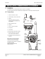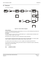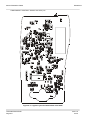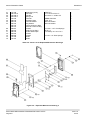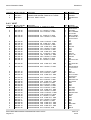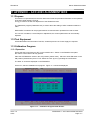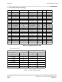
1
SP200/210
Service Manual
Published by Maxon Electronics Ltd
36a Gibson Avenue
Padstow Sydney
NSW Australia 2211
Tel: +61 (0) 2 9707 2000
Fax: +61 (0) 2 9707 3328
e-mail [email protected]
Internet: www.maxon.com.au
Any queries regarding information in this manual, please contact the Technical Services Group Leader at the above address.
Information provided in this document is believed correct at time of printing but is subject to change without notice.
Maxon will not accept liability for any loss, damage or costs howsoever caused as a result of the information provided.
SM-SP200/210
Maxon SP200/210 Radio
AMENDMENT RECORD SHEET
All amendments to this manual should be incorporated as soon as they are received and recorded below:
Issue No.
Effective Date
Reason for Change
Date
Signature
All Engineering Bulletins relevant to this product should be placed at the rear of this binder. Please ensure
that this manual is updated with any replacement pages, which may accompany these Engineering Bulletins.
Always read all Engineering Bulletins before carrying out work on a radio.
Please read the WARNINGS on the next page before referring to subsequent sections.
Issue 1.0
03/01
AMENDMENT RECORD SHEET
Page i
Maxon SP200/210 Radio
SP200/210
WARNINGS
•
Components containing beryllium oxide are used in the equipment. Dust from this material is a
health hazard if inhaled or allowed to come into contact with the skin. Great care must be taken
when handling these components. They must not be broken or subjected to excessive heat.
•
Never operate the radio transmitter without the correct Maxon antenna, or a suitable artificial
load, connected.
•
Never modify a radio, or accessory, except as instructed in the Service Manual, Engineering
Bulletins or formal communication as this may invalidate any warranty, guarantee or type
approval.
•
Do not operate this equipment in environments containing explosive materials or vapour.
WARNINGS
Page ii
Issue 1.0
03/01
SP200/210
TABLE OF CONTENTS
1
INTRODUCTION
1.1
1.2
1.3
2
SPECIFICATIONS
2.1
3
5
General
ACCESSORIES & OPTIONS
3.1
3.2
3.3
4
Using this Manual
Amendments to this Manual
Contact Information
Pre-Install Check
Accessories
Options
INSTALLATION, COMMISSIONING & ALIGNMENT
1-1
1-1
1-1
1-2
2-1
2-1
3-1
3-1
3-1
3-1
4-1
4-1
4-1
4-2
4-6
4-6
4-6
4-7
4-8
4-8
4-9
4-10
4-11
4-11
4-14
DETAILED FUNCTIONAL DESCRIPTION
5-1
TROUBLESHOOTING
6.1
Diagnostic Function
6.2
Troubleshooting Chart
6.3
Voltage Charts
6.3.1
Transistors (Main Circuit)
6.3.2
Integrated Circuits
7
Page Number
4.1
Installation
4.2
Connections
4.3
Commissioning
4.3.1
Test Equipment Connection
4.3.2
Transmitter Performance Tests
4.3.3
Receiver Performance Tests
4.4
Power Adjustment
4.5
Alignment
4.5.1
Preparation
4.5.2
Disassembly and Re-assembly of the Radio
4.5.3
PLL Alignment
4.5.4
Squelch Sensitivity
4.5.5
Transmitter Alignment
4.5.6
Receiver Alignment
5.1
Introduction
5.2
Common Circuits
5.3
Audio ASIC
5.3.1
Audio Signal Path
5.3.2
Sat Signal Path
5.3.3
Miscellaneous Signals and Controller
5.4
Audio/SAT Circuits
5.5
Common RF Circuits
5.6
Transmitter
5.7
Receiver
6
Maxon SP200/210 Radio
5-1
5-1
5-2
5-2
5-3
5-3
5-4
5-5
5-7
5-8
6-1
6-1
6-2
6-3
6-3
6-4
PROGRAMMING
7-1
7.1
SMP6100
7.1.1
Introduction
7.1.2
Getting Started
7.1.3
Programming
7-1
7-1
7-1
7-1
Issue 1.0
03/01
TABLE OF CONTENTS
Page iii
Maxon SP200/210 Radio
8
EXPLODED MECHANICAL DRAWINGS & PARTS LISTS
8.1
Parts List
8.2
Spare Parts
8.3
Mechanical Parts
8.4
SL100 VHF Parts List
8.4.1
V2 Control Circuit
8.4.2
V2 RF
8.4.3
TCXO Assembly
8.4.4
V2 VCO
8.4.5
V2 Front End
8.5
SL100 UHF Parts List
8.5.1
U2 Control Circuit
8.5.2
U2 RF
8.5.3
TCXO
8.5.4
VCO
9
CIRCUIT DIAGRAMS & PCB LAYOUTS
10
SPARE PARTS
10.1 Spare Parts
10.1.1 Component Replacement
11
APPENDIX – ACC-2003 ALIGNMENT BOX
11.1 Purpose
11.2 Test Equipment
11.3 Calibration Program
11.3.1 Operation
11.3.2 Adjustment of ASIC values
11.3.3 Transmit Adjustments
11.3.4 Receive Adjustments
11.4 Default Settings
11.4.1 V1 Band Default Settings
11.4.2 V2 Band Default Settings
11.4.3 U1 Band Default Settings
11.4.4 U2 Band Default Settings
SP200/210
8-1
8-1
8-1
8-3
8-8
8-8
8-10
8-13
8-14
8-14
8-15
8-15
8-17
8-20
8-21
9-1
10-1
10-1
10-2
11-1
11-1
11-1
11-1
11-1
11-4
11-6
11-7
11-8
11-8
11-9
11-10
11-11
LIST OF FIGURES
Figure 4-1 - Connections and controls............................................................................................................4-1
Figure 4-2 – Connections................................................................................................................................4-2
Figure 4-3 - Hirose connector .........................................................................................................................4-2
Figure 4-4 – Commissioning Test Setup using SK2055 Service Kit...............................................................4-2
Figure 4-5 – Commissioning Kit ......................................................................................................................4-3
Figure 4-6 – Test Equipment Set-up using Discrete Test Equipment ............................................................4-4
Figure 4-7 – Test Equipment Set-up using a Communications Test Set........................................................4-4
Figure 4-8 - SK 3100 Service Kit.....................................................................................................................4-5
Figure 4-9 - Back Panel Adjusters ..................................................................................................................4-7
Figure 4-10 - Removal of battery ....................................................................................................................4-9
Figure 4-11 - Replacing the battery.................................................................................................................4-9
Figure 4-12 – Replacing the battery................................................................................................................4-9
Figure 4-13 – Removing the belt clip ..............................................................................................................4-9
Figure 4-14 – Adjustment Points...................................................................................................................4-10
Figure 4-15 – ACC-2003 Alignment Box Test Setup ....................................................................................4-12
Figure 5-1 – ASIC Block Diagram ...................................................................................................................5-3
Figure 5-2 – Synthesiser Block Diagram ........................................................................................................5-5
Figure 5-3 - Transmitter Block Diagram..........................................................................................................5-7
Figure 5-4 - Receiver Block Diagram..............................................................................................................5-8
WARNINGS
Page iv
Issue 1.0
03/01
SP200/210
Maxon SP200/210 Radio
Figure 6-1 – Legend Layout for Top Side of Digital PCB ............................................................................... 6-5
Figure 6-2 - Legend Layout for Bottom Side of Digital PCB ........................................................................... 6-6
Figure 6-3 - Legend Layout for Top Side of RF PCB ..................................................................................... 6-7
Figure 6-4 - Legend Layout for Bottom Side of RF PCB ................................................................................ 6-8
Figure 8-1 - Exploded Mechanical Drawing 1................................................................................................. 8-3
Figure 8-2 - Exploded Mechanical Drawing 2................................................................................................. 8-5
Figure 8-3 – Exploded Mechanical Drawing 3 ................................................................................................ 8-6
Figure 9-1 – Digital Board Layout Top Side.................................................................................................... 9-3
Figure 9-2 - Digital Board Layout Bottom Side ............................................................................................... 9-4
Figure 9-3 - RF Board Layout Top Side.......................................................................................................... 9-5
Figure 9-4 - RF Board Layout Bottom Side .................................................................................................... 9-6
Figure 9-5 – Front-End Board Layout ............................................................................................................. 9-7
Figure 9-6 – VCO Board Layout ..................................................................................................................... 9-7
Figure 9-7 – TCXO Board Layout ................................................................................................................... 9-8
Figure 11-1 – Calibration Program Initial Screen ......................................................................................... 11-1
Figure 11-2 - Calibration Program Primary Screen ...................................................................................... 11-2
Figure 11-3 - ASIC Control Screen (Rx) ....................................................................................................... 11-3
Figure 11-4 - ASIC Control Screen (Tx) ....................................................................................................... 11-4
Figure 11-5 - ASIC Control Screen (Rx) ....................................................................................................... 11-5
Figure 11-6 - Modulation wave shape .......................................................................................................... 11-6
LIST OF TABLES
Table 6-1 – Diagnostics .................................................................................................................................. 6-1
Table 6-2 – Troubleshooting chart.................................................................................................................. 6-2
Table 6-3 - Main Circuit Transistor Voltages .................................................................................................. 6-3
Table 6-4 - Integrated Circuit Voltages (Receive) .......................................................................................... 6-4
Table 6-5 - Integrated Circuit Voltages (Transmit) ......................................................................................... 6-4
Table 8-1 - Parts List for Exploded Mechanical Drawing 1............................................................................. 8-4
Table 8-2 - Parts List for Exploded Mechanical Drawing 2............................................................................. 8-6
Table 3 – V1 Default Frequency Table ......................................................................................................... 11-8
Table 4 – V1 Default ASIC Settings.............................................................................................................. 11-8
Table 5 – V2 Default Frequency Table ......................................................................................................... 11-9
Table 6 – V2 Default ASIC Settings.............................................................................................................. 11-9
Table 7 - U1 Default Frequency Table........................................................................................................ 11-10
Table 8 - U1 Default ASIC Settings ............................................................................................................ 11-10
Table 9 – U2 Default Frequency Table....................................................................................................... 11-11
Table 10 – U2 Default ASIC Settings ......................................................................................................... 11-11
Issue 1.0
03/01
TABLE OF CONTENTS
Page v
Maxon SP200/210 Radio
WARNINGS
Page vi
SP200/210
Issue 1.0
03/01
SP200/210
Maxon SP200/210 Radio
1 INTRODUCTION
This Maxon Service Manual is a comprehensive guide to the maintenance and field repair of this
equipment. It covers a number of versions of the SP200/210 radio and its accessories. Differences
between the versions are indicated, as appropriate, in the text.
Before using this manual please read the whole of this introductory chapter, this will help you to make
the best use of it. If you have not done so already, please also read the warnings on page ii before
proceeding any further.
The range of SP200/210 radios is as follows:
SP200/210
199 fixed channel, (V2) VHF or (U2) UHF radio.
1.1 Using this Manual
At any one time you will need to refer to only a small part of the manual. It has been organised as
follows to make this as easy and as quick as possible.
Chapter 2 - Specification, gives the detailed specification.
Chapter 3 - Accessories and Options. Lists the Accessories and Options that are available.
Chapter 4 - Installation, Commissioning & Alignment. Describes connections to the radio, how to
commission it and how to Align the radio should this becomes necessary. You will also
find it helpful to read the operating instructions in the User Manual and Chapter 7 on
Programming.
Chapter 5 - Detailed Functional Description.
Chapter 6 - Troubleshooting and PCB Drawings.
Chapter 7 - Programming.
Chapter 8 - Exploded Mechanical Drawings and Parts Lists.
Chapter 9 - Circuit Diagrams and PCB Layouts.
Chapter 10 - Spare Parts & Maintenance Policy.
Chapter 11 – ACC-2003 Alignment Box
1.2 Amendments to this Manual
From time to time during its lifetime this product will be changed and improved. To cover such
changes, amendments to this manual will be issued in the form of replacement and/or additional
pages. It is important that anyone working on a product has all the relevant information. Therefore you
should incorporate amendments to this manual on receipt. Please follow the instructions
accompanying the amendment (in the form of an Engineering Bulletin) and be sure to complete the
amendment record at the front of this manual.
On occasion it may be necessary to issue product information more quickly than can be achieved with
an amendment. In this case the information will be distributed as an Engineering Bulletin. Engineering
Bulletin numbers are prefixed with a category letter – A, B or C. e.g.,
CATEGORY C - ENGINEERING BULLETIN 120
Issue 1.0
03/01
INTRODUCTION
Page 1-1
Maxon SP200/210 Radio
SP200/210
Category definitions are:
‘A’ Category A Engineering Bulletins will only be released if, by using the equipment manufactured
by Maxon or its subcontractors, a risk to operator safety or an infringement of Type Approval is
probable.
All units affected should be returned for modification to Maxon Europe Works Department on
receipt of such a Bulletin.
‘B’ Category B Engineering Bulletins are for equipment manufactured by Maxon that may have
component batch problems.
All equipment’s affected, that are in service, are to be returned to the Distributor or Dealer
workshop for modification. Maxon will supply replacement components free of charge.
‘C’ Category C Engineering Bulletins are for improvement or modification to equipment
manufactured by Maxon.
Dealer/Distributor to modify affected units in the field on the next service call. Maxon will supply
components free of charge.
Please place these at the back of this manual and refer to them before carrying out any work. This
Service Manual should be updated with any accompanying replacement pages. You may wish to
retain the previous issue pages for future reference.
1.3 Contact Information
Should you have any queries regarding this manual, or the information within it, please contact:
The Technical Support Group
Maxon Electronics Australia.
36a Gibson Aveune
Padstow Sydeny
NSW Australia 2211
Telephone: +61 (0) 2 97072000
Fax: +61 (0) 2 97073328
Technical Support e-mail: [email protected]
Internet: www.maxon.com.au
INTRODUCTION
Page 1-2
Issue 1.0
03/01
SP200/210
Maxon SP200/210 Radio
2 SPECIFICATIONS
2.1 General
Performance Specifications
R&TTE Appendix IV CE 168
ETS 300.086 Jan 91
I-ETS 300 219 Oct 93
ETS 300 279 Feb 96
TIA/EIA-603
Band
VHF
UHF
Channel Spacing
12.5kHz or 25kHz
Channel spacing is programmable.
RF Output Power
1W / 5W (programmable and variable)
Modulation Type
G3E
Audio Power
1W (Internal 4 Ω speaker)
500mW (External 8Ω speaker),
Intermediate Frequencies
45.1MHz First I.F.,
455kHz Second I.F.
Number of Channels
199
!
146 – 174MHz (V2)
440 – 470MHz (U2)
Switching Range (without retuning)
V2
U2
146 to 174MHz Rx
146 to 174MHz Tx
440 to 470MHz Rx
440 to 470MHz Tx
Frequency Source
Synthesiser
Operation Rating
Intermittent 90:5:5 (STBY:RX:TX)
Power Supply
7.5Vdc nominal
Current Consumption
Standby (muted) with battery save on
Standby (muted) with battery save off
Unmuted with 100% AF power
Transmit @ 5W RF output
<40mA
<80mA
<250mA
<2.4A
1350mAH
>8.5Hrs
Battery Life (minimum)
All figures stated with Power Save On
Issue 1.0
03/01
DRAFT
SPECIFICATIONS
Page 2-1
Maxon SP200/210 Radio
SP200/210
Environmental
Operating Temperature Range
Storage Temperature Range
-15 to +35°C (nominal)
-20 to +55°C (extreme),
-40 to +80°C (storage)
Charging Temperature Range
0 to +30°C
Humidity
EIA/TIA 603 (95%)
Protection against ingress of
dust and water
IEC 529 IP54
Vibration
BS2011 : Part 2.1Fc IEC 68-2-6
Part 2.1Fd IEC 68-2-34
Robustness
Mil Std 810 C Procedures I, II & V
ESD
20kV (C-MIC >= 15kV)
EMC
EMC Directive 89/336/EEC May 89
Physical Dimensions
112 x 61 x 40mm
(Excluding antenna and with QPA1350 pack)
Synthesiser
Reference Crystal
Frequency:
Holder:
Accuracy:
Ageing Rate:
12.8MHz
HC-18
± 3ppm over –30 to +60°C
< 2ppm / Year in the first year
< 1ppm / Year in subsequent years
Synthesiser Lock Time:
Switching Times
Tx to Rx, same frequency
Rx to Tx, same frequency
Rx to Rx
(over switching bandwidth)
Rx to Tx / Tx to Rx
(over switching bandwidth)
< 10mS
< 20mS
< 20mS
< 20mS
< 20mS
Receiver Sensitivity
<-118dBm (VHF), <-117dBm (UHF)
Squelch Sensitivity
7 – 12dB SINAD
Adjacent Channel Selectivity
Better than 70dB
Sub Audio Tones – CTCSS / DCS
Decode Sensitivity Method (decrease signal level @ 10% peak deviation)
All tones
<=9dB SINAD
CTCSS Tone Range
67 – 250Hz @ 0.3% accuracy
50 – 260Hz @ 0.3% accuracy (non-standard tones)
DCS Tone Standard
Standard & Inverted
Programmer
SPECIFICATIONS
Page 2-2
SMP 6100
DRAFT
Issue 1.0
03/01
SP200/210
Maxon SP200/210 Radio
3 ACCESSORIES & OPTIONS
3.1 Pre-Install Check
The SP200/210, as purchased, is supplied with an Antenna, charger and power supply, belt clip and User
Manual.
3.2 Accessories
A wide range of accessories are available for the SP200/210. The list below represents a summary of
accessories available at the time this manual was published. For up-to-date listings, and for price and
availability, please refer to the current Price Book.
Order Code
Description
Batteries
QPA-1350
1350mAh NimH battery.
Chargers
QPA-1185-2
QPA-1185-3
QPA-1185
QPA-1195-2
QPA-1195-3
CA1246
2-pin (European) Intelligent fast charger with mains adapter
3-pin (UK) Intelligent fast charger with mains adapter
Spare cup for the above chargers (No PSU)
6 + 6 Intelligent fast charger (Euro)
6 + 6 Intelligent fast charger (UK)
In-car charger
Speaker / Microphone accessories
MA100-01
Small Remote speaker mic.
MA100-02
Standard Remote speaker mic.
Headset Accessories
HS100-02
QPA1432
QPA1433
QPA1455
HS100-01
Lightweight headset
Lightweight headset
Two-way covert kit
Earbud
Earbud with Earhanger
Cases
CA1487
CA1475
CA1476
CA-7059
Lightweight Nylon case.
Soft Leather case
Soft Leather case with window
Belt Clip
Programmer
SMP6100
SP200/210 Programming Kit
3.3 Options
None
Issue 1.0
03/01
ACCESSORIES & OPTIONS
Page 3-1
Maxon SP200/210 Radio
ACCESSORIES & OPTIONS
Page 3-2
SP200/210
Issue 1.0
03/01
SP200/210
Maxon SP200/210 Radio
4 INSTALLATION, COMMISSIONING & ALIGNMENT
4.1 Installation
The SP200/210 is a hand-held radio and thus requires no installation.
The User should ensure that the batteries are charged before commencing commissioning tests.
4.2 Connections
1. Antenna connector: socket.
2. Channel Busy / Talk tri-colour LED.
3. Display
5
4. Main Power switch and volume
control. Fully anti-clockwise is the
OFF position.
BACK
5. Battery Release Catch.
6. Speaker.
7. Push To Talk (PTT) button.
8. Microphone.
9. Scan button.
4
3
2
1
10. Monitor button (unmutes the radio).
11. Channel select keys: Up / Down
keys, used to select channels.
6
12. Accessories socket (microphone &
speaker)
7
Note: Socket 12 is the Accessories
Connector, which may be used to
connect the radio to the following:
An optional remote speaker / microphone
An optional headset
A PC for programming using
SMP6100software
8
9
12
10
11
Figure 4-1 - Connections and controls
Issue 1.0
03/01
INSTALLATION, COMMISSIONING & ALIGNMENT
Page 4-1
Maxon SP200/210 Radio
SP200/210
The Accessory connector is wired as follows:
PTT / Mic
Ground
Speaker
Figure 4-2 – Connections
The small multi-pin connector, which is connected
to the other end of the test lead, is wired
as follows:
PTT / Mic
Screen
1
2
6
View from
5
rear of
connector
3
4
Speaker
Figure 4-3 - Hirose connector
4.3 Commissioning
This section covers the tests, which should be undertaken prior to handover of the radio to the end
user. All of the following tests can be carried out without having to gain access to the interior of the
radio.
Recommended Test Equipment
The alignment and performance test procedures assume the use of the following equipment. The
functions of most of the equipment may be found in a “Communications Test Set”. This type of
equipment is available from a number of test equipment manufacturers.
Throughout this book reference will be made to the use of the Communications Test Set. Where
applicable, the equivalent discrete item of test equipment may be used.
COMMUNICATION TEST SET
VOLT METER
.
RF
.
OSCILLOSCOPE
DEMOD
AF OUT
DC POWER SUPPLY
AF IN
TEST BOX
SK2055
RADIO
Figure 4-4 – Commissioning Test Setup using SK2055 Service Kit
INSTALLATION, COMMISSIONING & ALIGNMENT Page 4-2
Issue 1.0
03/01
SP200/210
Maxon SP200/210 Radio
Commissioning Equipment
2
1
3
5
4
Figure 4-5 – Commissioning Kit
Note: For those dealers who already have the SK2055 Service Kit (SL25/55) the audio cable (2),
CA8700, may be purchased. This interfaces the Service Kit to the SP200/210 and allows all simple,
commissioning audio measurements to be made. SMA adapter (5), ME210089 will also be required.
Flexi-pcb (3), ME110016 may be required if simple internal adjustments are to be made.
Note: The equipment shown in Figure 4-5 allows only VCO and power adjustments to be made to the
SP200/210. The full Service Kit, SK3100, is required for setting deviation.
Please refer to Figure 4-6 for the set-up using discrete test equipment and Figure 4-4 for the set-up
using the Communications Test Set. If the ACC-2003 Interface Box is used, please refer to
Figure 4-7.
Issue 1.0
03/01
INSTALLATION, COMMISSIONING & ALIGNMENT
Page 4-3
Maxon SP200/210 Radio
SP200/210
Discrete Test Equipment
RF Signal Generator (with CTCSS/1kHz
tone)
RF Power Meter
RF Frequency Counter
Spectrum Analyser and notch filter
(optional)
Audio Signal Generator
Audio Power Meter
SINAD Meter
Modulation Meter
Oscilloscope
Voltmeter
DC Power Supply, 0 - 10V 3A min.
Combined Equipment
Communications Test Set (e.g. Marconi
TF2955, Stabilock 4015 or similar).
Accessories
ME210089 SMA to BNC Adapter.
CA8700 Audio Lead for use with SK2055
Service Kit to perform audio
measurements.
SK3100 Service Kit
ACC-2002 SL100 Programming Lead
RF SIGNAL GENERATOR
WATT METER WITH
20dB ATTENUATOR
AUDIO POWER METER
AUDIO
MODULATION- METER
DISTORTION METER
TEST BOX
SK2055
DC POWER SUPPLY
RADIO
OSCILLOSCOPE
SINAD METER
AUDIO GENERATOR
SPECTRUM ANALYZER (optional)
154.625
VOLT METER
FREQUENCY COUNTER
Figure 4-6 – Test Equipment Set-up using Discrete Test Equipment
COMMUNICATION TEST SET
VOLT METER
.
RF
.
OSCILLOSCOPE
DEMOD
AF OUT
DC POWER SUPPLY
AF IN
INTERFACE BOX
ACC-2003
RADIO
Figure 4-7 – Test Equipment Set-up using a Communications Test Set
INSTALLATION, COMMISSIONING & ALIGNMENT Page 4-4
Issue 1.0
03/01
SP200/210
Maxon SP200/210 Radio
SK 3100 Service Kit
1
2
4
3
Figure 4-8 - SK 3100 Service Kit
This kit can be used for commissioning in the same way as the SK2055 (ignoring computer
connections). The above kit also includes a battery eliminator.
Note: If the Interface Box is used, ensure that it is set to manual, Audio enable is off and PTT is off
before powering up.
If programming the radio with the Battery eliminator connected, the curly cord must be disconnected
from the Interface Box.
The SK 3100 service kit is used with the
SP200/210 radio and provides most of the
interface cables and tools which will be required
for test and alignment of the SP200/210.
The SK 3100 Service Kit does not provide the
programming cable, ACC-2002. This is
available as part of the SMP6100
Programming Kit (see Section 3).
1. ACC-2003 Radio Interface Test Box. This
provides an audio interface, a battery
eliminator / programming interface and a
PTT switch.
2. ME210089 SMA to BNC Adapter
3. Trimmer Tools. These are used to adjust
the trimmers and ferrite cores within the
radio.
4. ME110016 Flexi-PCB. Used to
interconnect the Digital and RF pcbs for
servicing.
Issue 1.0
03/01
Prerequisites
For the following tests, signal generator
modulation level should be set to Average
System Deviation, i.e. 60% of maximum
system deviation.
The level should therefore be set to:
1.5 kHz for 12.5 kHz channel spacing
2.4 kHz for 20 kHz channel spacing
3.0 kHz for 25 kHz channel spacing
If the radio has had components installed to
change the channel spacing and/or operating
band from those installed at the factory,
ensure that the correct components are
installed in the receiver and transmitter stages
prior to testing.
Refer to the appropriate Electrical Parts List if
necessary.
INSTALLATION, COMMISSIONING & ALIGNMENT
Page 4-5
Maxon SP200/210 Radio
EEPROM programming
Ensure that the radio has the required
customer parameters programmed, otherwise
ensure that the radio is programmed with at
least the lowest, middle and highest Rx/Tx
frequencies prior to aligning the VHF and UHF
scanning handheld series radio.
Ensure that High and Low power are
programmed.
When CTCSS and DCS performance checks
are also required, ensure that the lowest,
middle and highest Rx/Tx frequencies include:
Lowest Rx/Tx freq. ch. 67.0 Hz CTCSS
Middle Rx/Tx freq. ch. DCS Code 072
Highest Rx/Tx freq. ch. 250.3 Hz CTCSS
The middle Rx/Tx frequencies should be
halfway between the lowest and the highest
frequencies.
SP200/210
e. Switch to a channel with a low power
and ensure that the nominal power is
1W ± 1.5dB.
Frequency Error
a. Check that the transmit frequency is within
+/- 500Hz (VHF) or +/- 750Hz (UHF) of
the frequency which is programmed
into the radio.
Deviation and Distortion
a. Set the radio to the middle Tx
frequency.
b. Set the audio signal generator to 1kHz
tone, low output impedance PTT and
adjust the AF generator level for 60%
system deviation:
12.5kHz channel spacing
20kHz channel spacing
25kHz channel spacing
c.
Programming details are given in Section 7.
4.3.1 Test Equipment Connection
Use a battery or connect the power supply
leads from the battery eliminator to the power
supply. The red, positive, lead connects to
+7.5Vdc. The black, negative, lead connects
to the negative, terminal of the power supply.
A connection diagrams are given in
Figures 4-4, 4-6 or 4-7.
Set the radio to a channel with High power.
4.3.2 Transmitter Performance Tests
Power Output
This test is only possible using the battery
eliminator.
a. Connect the transmitter to the
Communications Test Set (CTS).
b. Set the power supply to 7.5Vdc and
connect a dc voltmeter across the
power supply to monitor the supply
voltage.
c.
Set the CTS to the same frequency as
the radio. Activate PTT. Check and
record the power output. The nominal
power output is 5W ± 1.5dB (3.5 to 7W)
d. Reduce the power supply voltage to
6.0Vdc and PTT. The output power
should be greater than 50% of the level
measured above.
INSTALLATION, COMMISSIONING & ALIGNMENT Page 4-6
1.5kHz dev.
2.4kHz dev.
3kHz dev.
Measure the audio distortion. This
should be less than 5%.
d. Increase the audio signal generator
level by 20dB (10x voltage). The peak
deviation should be:
12.5kHz channel spacing <= 2.25kHz dev.
20kHz channel spacing
<= 3.6kHz dev.
25kHz channel spacing
<= 4.5kHz dev.
4.3.3 Receiver Performance Tests
Sensitivity
The SINAD performance test may be used to
test the sensitivity of the receiver.
a. Connect the Communications Test Set,
modulated with a 1kHz tone, to the
radio.
b. Set the frequency to correspond to the
Rx frequency of one of the channels
programmed into the radio.
c.
Using the Test Box, ensure that the AF
output from the Interface Box is connected
to the CTS SINAD meter.
d. Set the volume control to mid-range.
e. Set the Test Set deviation to:
12.5kHz channel spacing
20kHz channel spacing
25kHz channel spacing
f.
1.5kHz dev.
2.4kHz dev.
3kHz dev.
Adjust the RF signal generator level
until the SINAD meter reads 12dB.
Issue 1.0
03/01
SP200/210
g. Check that the signal generator RF
level is < -117dBm (UHF) or
< -118dBm (VHF).
Squelch
a. Ensure that both the radio and the
Test Set are set to the
appropriate channel spacing.
Maxon SP200/210 Radio
This section is included here as it is not
necessary to disassemble the radio in order to
set the power output.
A stable power source is required and
therefore the ACC-2003 Interface Box should
be used as this contains a battery eliminator.
For squelch adjustments, see Section 4.5.6.
b. With the above setting, reduce the RF
level to –130dBm. The radio should be
mute.
c.
Adjust the RF level until the SINAD
meter reads 10dB. The radio should
unmute. (Note: it will be necessary to
press and hold the monitor button to read
< 10dB SINAD).
20/25kHz
12.5kHz
Squelch
Audio Output
a. Set the RF signal generator to 1mV pd
(-47.0dBm) and the tone and deviation
as above.
b. Connect the audio power meter to the
external accessories socket on the
radio, via the test box.
c.
Adjust the volume control on the radio
under test to maximum (fully clockwise).
The voltmeter should indicate >= 1.55V.
The audio power meter should read
>= 300mW.
d. Decrease the volume control on the radio
so that the voltmeter reads 1.0V. Check
that the audio distortion is <5%.
High
Low
Power
Figure 4-9 - Back Panel Adjusters
a. Select a mid-frequency channel with
High Power.
b. Set the PTT switch to on.
c.
Adjust RV1 (High) to give 5W ± 0.1W.
d. Set the PTT switch to off.
e. Select a mid-frequency channel with
Low Power.
f.
Set the PTT switch to on.
g. Adjust RV3 (Low) to give 1W ± 0.1W.
Note: The audio power meter should be set to
8Ω.
h. Set the PTT switch to off.
This concludes the Performance Tests.
i.
If the Radio should fail any of these tests it will
be necessary to turn to the next section on
Alignment.
Repeat steps a to h until switching
between the two channels gives Low
Power of 1W and High Power of 5W.
j.
Switch to a low frequency, low power
channel.
k.
Set the PTT switch to on.
l.
Check that the power output is
1W ± 1.5dB (0.7 to 1.41W).
4.4 Power Adjustment
Note: Any power adjustments made should be
within R&TTE parameters.
Transmit periods longer than 5 minutes are to
be avoided.
Power setting potentiometers are located
underneath the upper label on the back of
the radio. A replacement label is shipped
with every radio.
Issue 1.0
03/01
m. Set the PTT switch to off.
n. Repeat steps k to m for a low power,
high frequency channel.
INSTALLATION, COMMISSIONING & ALIGNMENT
Page 4-7
Maxon SP200/210 Radio
SP200/210
4.5 Alignment
CAUTION
This radio contains static sensitive devices.
Static safe precautions should be observed, in
particular we would recommend the use of a
suitable floor mat, table mat, bonding cords
and a wrist strap. The soldering iron should
have an earthed tip.
Tests without Disassembly
Power Output, Deviation, Balance and
Squelch adjustment do not require the radio to
be disassembled.
Care should be exercised in the handling of
static sensitive components and they should
always be transported in the correct
containers.
Never remove, or insert, static sensitive
devices with the power applied.
4.5.1 Preparation
To perform the following tests it is necessary
to program the radio as follows:
VHF
Ch.
1
2
3
4
5
6
7
8
9
10
Tx(MHz)
146.025
160.025
173.975
173.975
173.975
146.025
160.025
173.975
173.975
173.975
Rx(MHz)
146.025
160.025
173.975
173.975
173.975
146.025
160.025
173.975
173.975
173.975
CTCSS
None
None
None
67Hz
250.3
None
None
None
67Hz
250.3
Tx(MHz)
440.025
455.025
469.975
469.975
469.975
440.025
455.025
469.975
469.975
469.975
Rx(MHz)
440.025
455.025
469.975
469.975
469.975
440.025
455.025
469.975
469.975
469.975
CTCSS
None
None
None
67Hz
250.3
None
None
None
67Hz
250.3
UHF
Ch.
1
2
3
4
5
6
7
8
9
10
Channel spacing as required. Channels 1 to 5
should be set to Low Power and channels 6 to
10 set to High Power.
Ensure that the Power Save is OFF.
INSTALLATION, COMMISSIONING & ALIGNMENT Page 4-8
Issue 1.0
03/01
SP200/210
Maxon SP200/210 Radio
4.5.2 Disassembly and Re-assembly of
the Radio
1
Radio
In order to carry out the following PLL and
Alignment procedures it will be necessary to
gain access to the inside of the radio.
Care should be exercised when opening up
the radio for maintenance or repair.
REMOVING AND REPLACING THE
BATTERY
Removal
Holding the radio chassis in one hand, press
and hold the battery release catch (1) on the
top of the battery pack.
Figure 4-10 - Removal of battery
Using the other hand, slide the battery down,
towards the bottom of the radio and off the
battery guide rail (2).
Replacement
With the slides of the battery positioned in line
with the radio battery rail guides, slide the
battery into position until a click is heard.
2
Figure 4-11 - Replacing the battery
REMOVING AND REPLACING THE BELT
CLIP
Removal
Lift the locking lever (3) located on the top of
the belt clip with one hand and pull the belt clip
out of the belt clip rail towards the battery /
radio top.
Replacement
With the slides of the belt clip positioned in line
with the belt clip rail guides, slide the belt clip
into position until a click is heard.
Figure 4-12 – Replacing the battery
3
Figure 4-13 – Removing the belt clip
Issue 1.0
03/01
INSTALLATION, COMMISSIONING & ALIGNMENT
Page 4-9
Maxon SP200/210 Radio
REMOVING AND REPLACING THE MAIN
ASSEMBLY
Removal
With the battery pack removed, there are four,
black, cross-head screws visible.
These can now be removed along with the
black, cross head screw holding the
accessories socket dust cover.
SP200/210
LOCATION OF ADJUSTMENT POINTS
Unscrew the antenna and slide off the volume
control knob.
Replace the battery but do not push all of the
way home. Gripping the lower sides of the
battery, and the lower sides of the radio lever
the two apart at the bottom of the radio to
separate the two.
C208
L203
TCXO
TP1
Withdraw the module from the case.
Remove the battery from the module.
This level of disassembly will be enough for
test purposes.
Note: A screwdriver, or similar object, should
never be used to force open the radio as the
sealing gasket is likely to be damaged.
To reassemble the radio, carry out the above
instructions in reverse, ensuring that the seal
is pushed down into the cover. Take care not
to damage the sealing gasket.
With the two parts of the radio separated, for
servicing, it will be necessary to link the two
pcbs using the flexi-pcb ME110016, which is
part of the Service Kit.
RF PCB
Figure 4-14 – Adjustment Points
4.5.3 PLL Alignment
Before any alignment is carried out to the
transmitter, or receiver, it is necessary to align
the Phase Locked Loop (PLL). The PLL
consists of the Rx VCO, Tx VCO and TCXO.
If the PLL is out of lock, an audible warning
will be heard UL will appear on the LCD
display.
Note: This alert will also be heard when a
channel is programmed out of the range of
operation of the radio, or it is not programmed
at all.
Note: If the power save parameter is
programmed there will be a periodic change at
TP1. Measurement should be based on the
steady state voltage, with power save off.
In order to carry out repairs, the two halves of
the radio may need to be linked using the flexipcb, ME110016.
This is part of the Service Kit and the Interface
Box and leads will also be required for some
of the tests.
Connect the radio under test to the Test
Equipment.
INSTALLATION, COMMISSIONING & ALIGNMENT Page 4-10
Issue 1.0
03/01
SP200/210
Rx VCO
a. Select Channel 1.
b. Check that the VCO tuning voltage at
TP1 is >5.7V +/- 0.25V (VHF) or >1.0V
+/- 0.25V (UHF).
c.
Select Channel 3
d. Check that the voltage at TP1 is <12.5V.
Tx VCO
a. Select Channel 1.
b. Set the PTT switch to on and check that
the voltage at TP1 is 1.0V +/- 0.25V
(VHF) or 2.0V +/- 0.25V (UHF).
c.
Maxon SP200/210 Radio
4.5.4 Squelch Sensitivity
The RF input level to open the squelch is
usually set in the range –123.5 to –117dBm
(0.15 to 0.3mV). The squelch should open at
a SINAD between 7 and 12dB (no CCITT).
The squelch should close between 2 and 4dB
of the value at which it opens.
RV2 sets the squelch level for 12.5kHz
channel spacing and RV4 sets the squelch
level for 20/25kHz channel spacing.
Note: RV2 MUST be set before RV4.
4.5.5 Transmitter Alignment
Power Adjustment
See Section 4.4.
Select Channel 3.
d. Check that the voltage at TP1 is <12.5V.
e. Set the PTT switch to off.
Note: If TP1 is below 0.6V or above 12.5V, in
any of the above tests, L203 may be adjusted.
L203 is covered in wax and therefore great
care will need to be taken when removing the
wax.
TCXO
a. Select Channel 2.
b. Set the PTT switch to on.
c.
Using the frequency counter, adjust the
TCXO control, so that the transmit
frequency is within +/- 200Hz of the
required frequency.
d. Set the PTT switch to off.
If no further alignment is to be carried out, it
may be necessary to check the squelch
setting.
Issue 1.0
03/01
INSTALLATION, COMMISSIONING & ALIGNMENT
Page 4-11
Maxon SP200/210 Radio
SP20/210
All further adjustments require the use of the ACC-2003 Alignment Box.
Refer to the ACC-2003 User Manual (on floppy disk) for operational information.
OSCILLOSCOPE
RADIOCOMMUNICATIONS
TEST SET
SERIAL DATA
DEMOD
AF IN
AF OUT
AUDIO
AUDIO IN
Power ATE
ACC-2003
INTERFACE
BOX
ATE
TXD
AUDIO
RXD
PTT
Power
AUDIO OUT
DC POWER SUPPLY
SERIAL DATA
7.5VDC @ 2.4A max.
Figure 4-15 – ACC-2003 Alignment Box Test Setup
Please refer to the ACC-2003 Interface Test Jig User Guide for details on how to use the ACC-2003
Interface Box.
The radio should remain programmed as Section 4.5.1 with ASIC values being read as per the
instructions.
Note: The ASIC programmer DOES NOT read frequency data, so only default frequencies will be
displayed even though the actual radio is programmed and operational on different frequencies.
Any adjustments to deviation and balance must be carried out in accordance to the R&TTE directive.
INSTALLATION, COMMISSIONING & ALIGNMENT Page 4-12
Issue 1.0
03/01
SP200/210
Maxon SP200/210 Radio
Balance Adjustment
a. Select Channel 3 (using software).
If necessary, adjust TXTRIM1 to keep within
the system deviation.
b. Set the audio generator to a 310Hz tone,
low output impedance, at a level of
400mV.
h. Press Shift + R to return to receive.
c.
Press Shift + T on the keyboard to
transmit.
d. Adjust TXTRIM2/TXTRIM3 to give a
square wave on the oscilloscope
(check that audio enable is ON on the
Interface Box.
CTCSS / DCS deviation
a. Select Channel 4.
b. Turn off the audio signal generator so
that the RF signal generator is not
modulated.
c.
Press Shift + T on the keyboard.
e. Press Shift + R to turn off the transmitter.
d. Adjust SATRIM2 for the desired CTCSS
tone peak deviation (± 50Hz) which is:
Audio deviation adjustment
a. Select Channel 3 and press Shift + T to
turn on the transmitter.
12.5kHz channel spacing 0.25kHz dev.
or 20kHz channel spacing0.4kHz dev.
or 25kHz channel spacing0.5kHz dev.
b. Set the audio generator to 1kHz and
adjust its level for 60% peak system
deviation. Ensure that, depending upon
the channel spacing of channel 3, the
deviation is either:
e. Press Shift + R to return to receive.
12.5kHz channel spacing 1.5kHz dev.
or 20kHz channel spacing2.4kHz dev.
or 25kHz channel spacing3kHz dev.
f.
Select Channel 5.
g. Press Shift + T and check that
the deviation is the same as above.
If the deviation is greater than above,
adjust SATTRIM2.
h. Press Shift + R to return to receive.
c.
Measure the audio distortion. This
should be less than 5%.
d. Increase the audio level by 20dB (10x
voltage).
i.
Select Channel 4.
j.
Press Shift + T to transmit.
k.
Turn the audio generator back on so that
the RF signal generator is modulated
with a 310Hz tone.
e. Adjust TXTRIM1. to set the deviation to:
12.5kHz channel spacing 2.25kHz dev.
or 20kHz channel spacing3.6kHz dev.
or 25kHz channel spacing4.5kHz dev.
f.
Slowly sweep the audio signal generator
between 300Hz and 3kHz. Record the
peak deviation. The peak deviation
should be:
12.5kHz channel spacing <= 2.5kHz dev.
or 20kHz channel spacing<= 4kHz dev.
or 25kHz channel spacing<= 5kHz dev.
If necessary, adjust TXTRIM1 to keep within
the system deviation.
g. Repeat para. f with the radio set to
Channel 1.
12.5kHz channel spacing 2.5kHz dev.
or 20kHz channel spacing4.0kHz dev.
or 25kHz channel spacing5.0kHz dev.
l.
Press Shift + R to return to receive.
Select Channel 5 and press Shift + T.
Check that the peak deviation is less than:
12.5kHz channel spacing <= 2.5kHz dev.
or 20kHz channel spacing<= 4.0kHz dev.
or 25kHz channel spacing<= 5.0kHz dev.
If necessary, adjust TXTRIM to keep within the
system deviation.
m. Press Shift + R to return to receive.
n. Write the changes to the radio.
Issue 1.0
03/01
INSTALLATION, COMMISSIONING & ALIGNMENT
Page 4-13
Maxon SP200/210 Radio
SP200/210
This completes the transmitter alignment
process.
4.5.6 Receiver Alignment
Audio Volume Level
a. Set the test set to the appropriate
frequency at –47dBm with 1kHz tone
modulation at 60% system deviation:
12.5kHz channel spacing 1.5kHz dev.
or 20kHz channel spacing2.4kHz dev.
or 25kHz channel spacing3kHz dev.
b. Select Channel 1.
c.
With the calibration program running on
the PC, select Rx_Vol.
d. Turn the volume control to maximum.
e. Using the PageUp and PageDown keys,
press until the desired maximum volume
level is achieved.
Note: -17.5dB corresponds to 2.10V (+/-0.2V)
into 4 ohm speaker.
At maximum volume, nominal distortion is
10%.
f.
Write the changes to the radio.
It may be necessary to carry out adjustment of
the squelch setting, see Section 4.5.4.
This completes the receiver alignment
process.
The following parameters would NOT normally
be adjusted unless specific environmental
conditions necessitate a change:
INTRIM on the receiver (Audio from IF IC.)
SATRIM on the receiver (gain received – sub
audible tone)
Refer to the ACC-2003 User Guide for details.
INSTALLATION, COMMISSIONING & ALIGNMENT Page 4-14
Issue 1.0
03/01
SP200/210
Maxon SP200/210 Radio
5 DETAILED FUNCTIONAL DESCRIPTION
5.1 Introduction
This section provides a detailed description of the operation of the radio.
5.2 Common Circuits
Power Circuits
Battery voltage, or external voltage through the accessories connector, is applied via a 4A fuse (plus
diode protection) directly to the RF power module and, after the on/off switch, to the dc to dc converter
and voltage regulator. The majority of the circuitry is powered via IC1, which regulates the +7.5V dc
supply down to +5V.
Transistors Q2 and Q32, in conjunction with the Tx Enable and Rx Enable lines from the
microcontroller, apply +5V Tx or +5V Rx to the relevant circuitry during receive or transmit. Thus, for
instance, the receive front end amplifier is only powered during receive and the power control IC is
only powered during transmit.
It is possible to program the radio for power saving. This mode causes the microcontroller to pulse the
Rx Enable line high and low for periods between 100 and 300mS. The time may be selected when
programming the radio. As soon as the radio detects a signal it switches into normal mode.
Microcontroller
The microcontroller (IC403) is a One Time Programmed Processor chip based on the Hitachi HD3837
processor with onboard ROM and RAM.
It controls all functions performed by the radio, in conjunction with control signals from push buttons,
switches etc. It controls the data to/from the EEPROM and to the PLL IC, Audio ASIC as well as
controlling external data from the programmer and alignment interface. The microcontroller generates
the enable lines, controlling routing of signals and the indicators (LED,LCD and bleeps).
The microcontroller also generates and decodes the SAT tones (filtered by the ASIC).
EEPROM
Relevant channel information, such as Rx / Tx frequencies and CTCSS / DCS codes, is stored in the
EEPROM (IC404) which is a X25330. This information may be programmed and erased via the
accessories socket. Certain parameters can also be altered via the pushbuttons and keys on the
radio, i.e. scan channels and priority channel. The EEPROM has 32768 (8x4096) capacity and data is
written serially.
Channel Select Circuit
Up to 199 channels may be selected, using the channel keys on the front panel. Pressing the channel
keys earths pins 40 and 41 of the microcontroller, so enabling the decoding for the appropriate Rx and
Tx frequencies, and associated data, to be selected from the EEPROM.
Issue 1.0
03/01
DETAILED FUNCTIONAL DESCRIPTION
Page 5-1
Maxon SP200/210 Radio
SP200/210
5.3 Audio ASIC
The audio ASIC (IC406) processes both the audio signal and the sub-audible tones, including filtering,
amplifying, setting attenuations levels etc. It is a programmable device, controlled by the
microcontroller, hence alteration of deviation levels is achieved by the ACC-2003 Alignment Software.
The internal block diagram is shown in Figure 5-1. The audio and SAT routes within the ASIC will be
described separately.
5.3.1 Audio Signal Path
A1
A2
ASW1
INTRIM
300Hz HPF
ASW2
DE-EMPHASIS
PRE-EMPHASIS
RXVOL
AMP
LIMITER
ASW3
VLPF
TXTRIM1
TXSUM
ATTN
TXTRIM2/3
A3/A4/INV
Buffers discriminator audio input from Pin 30 (INI) and passes it to
Analogue Switch 1 (ASW1). It has a gain of x1.
Amplifies the analogue signal from the mic input terminal (IN2) and
passes this signal to Analogue Switch 1. It has a gain of 10dB.
This is a two-way analogue switch. It is controlled by the serial control
interface. Default value is 0, which is Rx (A1).
Sets the deviation for the input analogue signal sensitivity. The control
range of this device is –3.5 to +4dB controllable in 16 steps. The
control is a 4 bit signal where the default value is 1000, which
corresponds to 0dB.
th
Comprises an 8 order filter with a cut-off frequency of 300Hz.
Attenuation of the unwanted is at least 30dB.
This is a four-way analogue switch, controlled by the serial control
interface. It passes the received audio to the de-emphasis circuit or
the transmit audio to the pre-emphasis circuit. Alternatively, the preemphasis or de-emphasis can be bypassed. The control signal is a 2
bit signal with 00 as the default, which is de-emphasis.
Applies de-emphasis to the received audio at 6dB/octave. At 1kHz, the
gain is x1.
Applies pre-emphasis to the transmit audio at 6dB/octave. At 1kHz,
the gain is x1.
Controls the magnitude of the Rx audio signal which is passed, via the
volume control (VR5) to the speaker in 16 steps from 0dB attenuation
up to 37.5dB attenuation, to Rxout on pin 28.
This amplifier provides gain, to the Tx audio, in 8 steps from +20dB to
+41dB.
Applies limiting at 0dB (2.8V p-p). The output of this stage is controlled
in 4 steps from 0dB to –5.4dB attenuation by a 2 bit control signal.
This is a two-way analogue switch, controlled by the serial control
interface. It passes the Tx audio, or the SAT to the low-pass filter.
th
This is a 6 order low pass filter, which is controlled by the serial
control interface. The cut-off point is switched between 2.55kHz and
3kHz.
Provides deviation adjustment of Tx audio in 16 steps from +3.5dB
gain to –4dB attenuation. Uses a 4 bit control signal.
Mixes (Adds) the signal from TXTRIM1 with the SAT signals from
COMPIN+, or selects one or other of the signals. Can also apply 50dB
muting. Controlled by the serial control interface.
Attenuates the signal from TXSUM by either 0dB or 6dB.
Signal follows two routes (to VCO & TCXO) for final deviation
adjustment in 32 stages from +3.75dB to –4dB. Controlled by 5 bit
signal.
Final output buffer amplifier for Tx analogue signal. Gain is 0dB. A3
output (modout 1 on pin 1) goes to the VCO and A4 (modout 2 on pin
2) goes to TCXO, are non-inverting outputs. The inverting output (INV)
from A4 is not used.
DETAILED FUNCTIONAL DESCRIPTION
Page 5-2
Issue 1.0
03/01
SP200/210
Maxon SP200/210 Radio
5.3.2 Sat Signal Path
ASW4
VSCLPF
SATRIM1
SATRIM2
COM
ASW4 switches between RxSAT (RDIN) and Tx SAT (TXIN) and
routes to the filter.
Seventh order Elliptic Variable Switched Capacitor Low Pass Filter.
Cut-off frequency is variable from 50Hz to 300Hz. Level adjustable in
0.5dB steps from –3dB to +2.5dB. Output is on pin 23 FLT OUT.
Not used.
SAT level adjustment. Amplitude is controlled in 0.5dB steps from –
3dB to +2.5dB. Output is on pin 23 FLTOUT.
Compares the external reference voltage (COMPPIN-) with the applied
SAT signal which is from FLTOUT to COMPIN+ and it goes to Logic
High and Logic Low at this point. The output COMPOUT (pin 21) goes
to the microcontroller IC406. NB in transmit the SAT is switched into
TXSUM.
5.3.3 Miscellaneous Signals and Controller
ADC / DAC
CONTROL
DATA
CLOCK
ENBL
AGND.DGND
ADC is not used. DACs are 8 bit devices.
Control serial interface for control lines.
Operates as output line for a READ instruction and as input line for a
WRITE instruction, Pin 18.
This is the synchronous input terminal for communication with the
microcontroller, pin 12.
With an active low, data read and write is enabled.
Reference analogue and digital grounds.
Figure 5-1 – ASIC Block Diagram
Issue 1.0
03/01
DETAILED FUNCTIONAL DESCRIPTION
Page 5-3
Maxon SP200/210 Radio
SP200/210
5.4 Audio/SAT Circuits
CTCSS / DCS Decoder Circuits
Discriminator audio from pin 9 IC5 is applied, via IC408D, to pin 3 of the audio ASIC. The audio
th
frequencies of the signal are filterecd out by the 7 order Elliptic Low Pass Filter, leaving only the SAT
audio tones. The level is then set by the ASIC and is routed via IC407A back to the ASIC for
comparison with a reference voltage. This produces the logic data signal. This logic signal on pin 21
(IC406) is fed into the microcontroller (IC403) where it is matched with a programmed frequency. If
there is a successful match, decode occurs, which is shown by a green LED on the top of the radio
and audio is heard. If there is an invalid decode, the LED will light yellow (BUSY)
CTCSS / DCS Encoder Circuits
During TX encode the tone squelch digital signal is produced as a 3-bit parallel word at pins 48, 49
and 50 of the micro controller (IC403). The 3-bit digital signal is converted to an analogue signal by
resistors R420, 421 and 423. The analogue signal is fed into IC406 pin 4 where it is filtered and its
deviation level is set.
The filtered encode output from pin 23 (IC406) is fed back into pin 22 (IC406) via IC407a (LM358).
The filtered encode signal is mixed with the audio signal from TXTRIM1 by TXSUM. Via ATTN, the
mixed signals are applied to TXTRIM2/TXTRIM3, which controls the modulation to the VCO and
TCXO respectively (see RF description).
External Mic / PTT Control Circuit
The external microphone is connected via a 3.5 mm stereo jack socket on the right-hand side of the
radio. The internal mic and speaker are disabled when the external connector is plugged the
SPK/MIC jack socket.
When the external PTT is depressed, a low impedance is presented to the base of Q403 (below 20k
ohm). Q402 and Q403 switch on and so Q402 collector is low (normally tied high). This point is
connected to IC403 (microcontroller) pin 43 (PTT). The same point is connected to the normal PTT
button, SW403, which is earthed when depressed.
The mic audio itself is switched through IC401A by the Tx enable line to IC408D amplifier stage and
through to the audio ASIC for filtering and deviation level setting. As described previously, this audio
signal is added to the SAT and routed to the TCXO and VCO.
Rx Audio
The discriminator audio is fed directly into the audio ASIC from the RF section (see later). The ASIC
sets the gain and filters out any SAT. The output is fed to the volume control (VR5). The alert tones
and switch on melody is routed from the microcontroller via link LK27 to the same point to the volume
control.
The AF from the volume control is fed to the audio amplifier, a TDA7233, which is activated by the
mute circuit. The output is then fed to the internal or external speaker.
Mute Circuit
The microcontroller (IC403) has a mute circuit which is output on pin 13 (7233EN). The operation of
the mute depends upon a number of factors, such as is the demodulator receiving a mute signal from
the FM detector and does the signal have the correct CTCSS / DCS. The microcontroller will also
change the state of the mute if the monitor button is depressed (SW402), assuming that this function
has been enabled in the programming
Pin 13 is connected to Q414, Q415 via R446, which mutes the TDA7233IC.
DETAILED FUNCTIONAL DESCRIPTION
Page 5-4
Issue 1.0
03/01
SP200/210
Maxon SP200/210 Radio
Battery Low Indicator Circuit
When the battery voltage drops below 5.6 VDC a Battery Low indication is given. Due to the volts drop
across D403, a voltage below 5.6V on the battery gives a voltage less than 5V on the base of Q405. ,
Q405 switches on its when base is below 5v (current flow through R413), which switches on Q404, so
driving pin 52 of the microcontroller low (normally tied high). The micro controller disables the
transmitter and at the same time enables the red LED and sends an alert tone to warn the user. The
battery should be replaced or recharged at this time (one transmission is allowed after the low battery
warning).
LEDs and indicators
The red and green LEDs are switched on, via Q407and Q411, by control lines from the
microcontroller. Both the red and green LEDs being lit indicate the condition ‘busy’ i.e. orange. Both
the LCD and backlight are driven from the microcontroller.
The alert tones are generated in the microcontroller and are fed through a filter to the volume control
via link 27. There is an option of routing the tones directly to the audio amp via link28.
5.5 Common RF Circuits
PLL Synthesiser
The PLL synthesiser circuit is common to both the transmitter and receiver.
The synthesiser comprises:
TCXO
DC - DC
Converter
Loop Filter
Data
IC 2
PLL
Charge Pump
Tx or Rx
VCO
~
RF Out
Figure 5-2 – Synthesiser Block Diagram
12.8 MHz TCXO
The TCXO contains a crystal oscillator, which has 2-stage thermistor network compensation, and a
modulation port. Accuracy is +/-2.5 PPM from -30°C to +60°C. Frequency adjustment is provided by
TC701.
VCO
The VCO is configured as a Colpitts oscillator using transistor Q202, varactor diodes D201 / 202,
frequency setting inductor L203 and associated components. Cascade bias is provided by Q201.
The frequency of operation is controlled by reverse biasing D201 in the range of 1 to 12 V dc (from the
PLL). During receive Q9 is switched on by the Rx enable (active low), so switching D203 in circuit (via
Q203), which puts C208 (variable capacitor) in parallel with the varactor diodes and adjustable
inductor.
Issue 1.0
03/01
DETAILED FUNCTIONAL DESCRIPTION
Page 5-5
Maxon SP200/210 Radio
SP200/210
In transmit the VCO has modulation from the audio processing circuitry applied to D202. C204 is used
to provide compensation for non-linearity caused by the modulation diode and maintains a constant
modulation regardless of the frequency of operation.
PLL IC
The reference frequency from the TCXO, at 12.8 MHz, is connected to pin 20 of IC2 (MC145191).
The appropriate VCO is connected to pin 11.
The external reference frequency, TCXO input, is divided by the reference divider (REFDIV), which is
set to divide by 2048 for 12.5kHz or 25kHz channels (6.25kHz) or to divide by 2560 for 20kHz
channels (5kHz). This is known as the reference frequency, Fr.
The comparison frequency is determined by the settings which are stored within the EEPROM
(IC404). Choice of these comparison frequencies means that the minimum step size of the synthesiser
is either 5kHz or 6.25kHz and therefore, 12.5kHz, 20kHz and 25kHz channel spacings can be
accommodated.
IC2 is programmed on pin 19, to obtain the desired frequency, by serial data from the microcontroller
(IC403 pin 21). IC2 Pin 19 is the data input and pin 18 is the clock input and pin 17 is the PLL enable
line.
The VCO frequency, Fin, is divided down by the programmable divider (64/65 prescaler VARDIV) to,
again, produce 5kHz or 6.25kHz. This frequency is known as the variable frequency, Fv.
In the phase/frequency comparator, the phase difference between the reference frequency, Fr, and
the VCO signal, Fv, is compared.
When Fv = Fr, the phase detector output (pins 3 and 4, IC2) produces narrow negative pulses and Fv
and Fr pulse widths are identical. When Fv > Fr, pin 4 (V) pulses negative, with pin 3 (R) remaining
high. When Fv < Fr, pin 3 (R) pulses negative with pin 4 (V) remaining high. The signal at pins 3 and
4 is smoothed by the loop filter and applied to the VCO.
Out-of-Lock Detector
The out-of-lock detector output remains essentially high with narrow low-going pulses when in lock.
The output pulses low when Fr and Fv are out of phase or at a different frequency (results in wider
pulses). These pulses at pin 2 are buffered by Q5 and then integrated by R1 and C11. The resultant
voltage is fed to the microcontroller, IC403, pin 53.
IC2 has two output ports:
Port A pin 16
Port B pin 15
Configurable digital port, which is used as tx enable 2, which controls the application
of volts to the PA stage.
Open drain digital output, which is used as a power save control.
Pin 13 labelled test2 allows the technician to see the output of the dual modules prescaler for trouble
shooting purposes, no connection should be made to this pin.
Charge Pump and Loop Filter
Transistors Q6 to Q8 and Q11, and associated components, form the charge pump. The phase
detector output from IC2 pins 3 and 4 are combined by the charge pump to produce a 0 to 12V tuning
voltage.
The voltage signal is filtered by the loop filter (R12 – R14, C21 - C24) to remove harmonics of the
reference frequency.
DC to DC Converter
The DC to DC converter, converts the +7.5 V to a 16 V suppy. This is used to provide the tuning
voltage for the VCO. A wide voltage range is required to allow for the wideband operation of the radio.
Q904, Q905 and associated components, form a 200kHz oscillator. The output of the oscillator is
rectified (voltage tripled) by D901, D902 and D903. C901, C902 and C916 provide filtering. The
resultant 16Vdc is passed to R909 and then becomes the supply rail for the charge pump.
DETAILED FUNCTIONAL DESCRIPTION
Page 5-6
Issue 1.0
03/01
SP200/210
Maxon SP200/210 Radio
5.6 Transmitter
The transmitter comprises:
Figure 5-3 - Transmitter Block Diagram
Buffer
The RF output level from the VCO is 0dBm. This is amplified to +17dBm by the buffer amplifier
consisting of Q16, Q17, Q3 and associated components. All stages are simple common-emitter
amplifiers with resistive biasing and tuned collectors. A pi-type attenuator (R31, 32 and 34) is used
between the two stages.
PA module
The PA module consists of a hybrid amplifier. Pin 3 is permanently connected to the battery voltage
and pin 2 is connected to the supply when switched by Q22, which is controlled via the power control
circit by the Tx enable line. The RF input is on pin 1 and the output is on pin 4.
Low pass filter
L7, L8, L11, C73, C74, C75 and C76 form a 7th order Chebyshev low pass filter. Unwanted
harmonics are reduced by 65dB.
Antenna Switch
When transmitting, the diodes D5 and D6 are forward biased, allowing the RF to pass to the antenna.
D6 is shorted to ground which makes L13 look open circuit (1/4 wave tuned stub). This prevents the
Tx signal from passing to the receiver stage.
In receive, the diodes D5 and D6 are reverse biased. L13 is now in circuit, passing the signal from the
antenna to the front end without signal loss.
Automatic power control (APC) circuits
The APC circuit consists of IC3B, Q19, Q21, Q22 and associated components. The PA supply current
passes through R109. Variations in power output, produce variations in supply current, which is
amplified by IC3A and Q19.
The voltage on the wiper of RV1 is passed to IC3B and compared with the fixed reference voltage
developed by the potential divider R45 and R46. The output of IC3B, pin 7, controls Q21 and Q22 to
provide supply voltage to the PA driver transistors Q501 and Q502. RV3 controls the low power
setting and is switched into circuit by Q23.
A change in PA output will result in an inverse change in driver supply voltage maintaining a constant
RF output.
Issue 1.0
03/01
DETAILED FUNCTIONAL DESCRIPTION
Page 5-7
Maxon SP200/210 Radio
SP200/210
5.7 Receiver
The receiver comprises:
Rx
VCO
Local
Oscillator
~
~
Audio
Filter
Audio
Amplifier
FM LimiterDiscriminator
Squelch
Circuit
Figure 5-4 - Receiver Block Diagram
Antenna Switch
In receive, the diodes D5 and D6 are reverse biased. L13 is now in circuit, passing the signal from the
antenna to the front end without signal loss.
Front End
The receive signal is routed to the RF Front End module, pin 1. It passes through a matching circuit
consisting of C601 to C603 / L601 & L602.
Diode D601 serves as protection from RF overload from nearby transmitters.
The input signal is coupled to the base of Q601 which serves as an RF amplifier. The output of Q601
is then coupled to a bandpass filter consisting of C604 to C620 / L603 to L607.
The output of the front end module, pin 6, is then coupled to the double-balanced mixer D9.
The receiver front end module is factory pre-tuned and requires no adjustment. Repair is effected by
replacement of the entire module.
The modules are:
VHF
UHF
146 MHz to 174 MHz
440 MHz to 470 MHz.
DETAILED FUNCTIONAL DESCRIPTION
Page 5-8
Issue 1.0
03/01
SP200/210
Maxon SP200/210 Radio
First Mixer
D9, T1 and T2 form a double balanced mixer which provides the 45.1MHz intermediate frequency
output. The filtered frequency from the front end module is coupled to T1.
The Local oscillator input from the VCO is coupled to T2.
The output of the mixer is taken from the tap on transformer T1 and fed to the single pole diplexer,
comprising L15 / C93 and R65 (High-pass terminating filter) and L14 / C92 (Low-pass coupling filter)
The 45.1MHz crystal filter provides a bandwidth of +/-7.2 kHz. This filter provides a high degree of
protection from spurious and intermodulation products. Additionally, a 90 MHz trap (C93 / L15) is
placed at the filter input.
The output of the filter is coupled by C43 to the base of the post filter IF amplifier Q25.
Second mixer, Second IF, FM detector
The output of the IF amplifier is fed into the narrowband FM IF Integrated Circuit, IC5 (MC3372). This
is a single conversion FM receiver which contains the second mixer, second IF amplifier, and FM
detector.
The second local oscillator frequency is determined by the crystal X1 connected to pin 1 of IC5. In this
case the crystal has a frequency of 44.645MHz. The first IF signal is applied to the mixer and the
resultant frequency of 455KHz, is the difference between the IF signal and second local oscillator.
The 455KHz IF signal is output from pin 3 and is applied to a 455KHz band-pass filter, CF1 (20/25 kHz
channel spacing) or CF2 (12.5 kHz channel spacing). The selection of the filters is accomplished by
diodes D13 (input) and D14 (output) whose bias is controlled by the N/S SW line on the
microcontroller (IC403, pin 25).
The microcontroller takes the relevant channel spacing data from the EEPROM. A High on the N/S
SW line switches the 455kHz signal to CF1, a low switches the signal to CF2.
The output of the relevant IF filter is passed to pin 5, which is the input to the limiting amplifier.
The limiting amplifier is biased externally by R19 & R95 and connected by C52 to the quadrature
detector (X2). The output connects to pin 8. The quadrature circuitry provides a 90° phase shift at the
IF centre frequency, which enables audio to be recovered. Any detected signal is produced at pin 9 of
IC5 and applied to the Receiver Audio Circuit and the Mute (Squelch) Circuit.
Squelch (Mute) Circuit
The mute circuit switches off the audio amplifier when no audio signal is present. The squelch circuit
consists of IC5 and RV2 (RV4) and their associated components. The noise signal from pin 9 of IC5
is amplified by an internal amplifier in IC5 and fed to the 16kHz bandpass filter.
16kHz Band Pass Filter
The audio signal from pin 9 of IC5 is filtered by a 16 kHz band pass filter consisting of L16, L17 / C111
to C113. The noise in the IF passband is accepted and voice frequencies and their products are
rejected.
Any noise present at the output of the filter is applied to the noise detector circuit via RV2 (RV4). RV2
(RV4) is used to adjust the squelch circuit sensitivity and is normally adjusted to produce a noise
squelch opening sensitivity of 10 to 12 dB SINAD.
For 12.5 kHz channel spacing, RV4 is switched in, by the microcontroller and Q28, to attenuate signal
at RV2 for 25 kHz channels. A High on the N/S SW line switches in RV4.
The output from the band pass filter is applied to the filter amplifier input on pin 10 of IC5.
Issue 1.0
03/01
DETAILED FUNCTIONAL DESCRIPTION
Page 5-9
Maxon SP200/210 Radio
SP200/210
Noise detector circuit
The noise detector circuit, in conjunction with IC5, consists of transistors Q26, Q27, thermistor TH1
and diode D11. Any noise signal present is applied to Q27 from pin 11 of IC5. The signal is amplified
by Q27, rectified by D11 and then buffered by Q26. The buffered signal is applied to pin 12 of IC5
(Squelch input).
The squelch trigger output (pin 14, IC5) is applied to the microcontroller BUSY input on pin 54 of
IC403. The actual audio mute is from the microcontroller.
When noise is present, the voltage at pin 12 of IC5 (Squelch input) exceeds 0.7V. This causes the
squelch trigger output to go open circuit, which turns on Q24 and the busy line goes low, which mutes
the receiver audio circuit.
When no noise is present, the voltage at pin 12 of IC5 is less than 0.7 V and pin 14 of IC5 is
grounded, which switches Q24 off, so the busy line goes high, unmuting the receiver audio circuit.
Resistor R74 is used to provide hysteresis of 3 to 6 dB.
AF Output Low Pass Filter
A low pass filter formed by C115, C116 and R91 removes any extraneous 455 kHz energy from the
AF output of the FM receiver chip.
Speaker Audio Amplifier
After signal detection and audio filtering the signal is passed to the digital board, to the audio ASIC
(via IC408 for SAT). ). After the audio ASIC (see previous description) the signal is then routed, via
the volume control (VR5), to pin 8 of IC402. IC402 is a TDA7233 audio amplifier, which is enabled by
the control line from the microcontroller via Q415 and Q414.
DETAILED FUNCTIONAL DESCRIPTION
Page 5-10
Issue 1.0
03/01
SP200/210
Maxon SP200/210 Radio
6 TROUBLESHOOTING
This section includes voltage and troubleshooting charts which should assist the engineer to isolate
and repair the fault. Voltage measurements should be made using a high-impedance voltmeter and
the values given are with respect to ground.
Obvious checks, such as battery performance on load, should be made before pulling the radio apart.
Substitution of another set of batteries, or the use of a power supply, isolates this cause.
The alignment procedures, given in Section 5, list how standard tests such as SINAD measurements
can be made. These can be used to check the performance of the receiver.
Careful alignment, using suitable test equipment, and quality interface cables should ensure that the
radios meet their specified performance.
6.1 Diagnostic Function
The diagnostic function is designed to inform the user about the operational status of the radio.
The possible audible and visual warnings are:
Status
Normal
Description
Power On Ready
Busy
Correct S.A. Tone
Transmit
Transmit Not Allowed
LED Colour
N/A
Yellow
Green
Red
Red Flashing
Scan
Priority Scan Mode
Priority Lookback
Flashing Green
Green Flashing
Green Flashing
Priority
Edit
Scan Edit
Edit Priority Channel
SE
N/A
Warning
Time-Out Timer
Two Red
Flashes
Single Red
Flash
N/A
Pt
Busy Lock
Tx Inhibit
Battery Low
EEprom
PLL Error
Flashing Yellow
N/A
Flashing Red
N/A
N/A
bL
_h/r0
LC
Er
UL
Single Tone/Triple
Tone Repeated
Repeating Single Tone
Two Beeps
Repeating Triple Tone
Repeating Single Tone
Repeating Dual Tone
Scanning
Error
Edit Scan List
LCD Indication
188
Channel Number
Alternating UL
with Channel No.
N/A
Lb/Channel
Number
PE
Audible Tone
Melody
N/A
N/A
N/A
Repeating Dual Tone
N/A
N/A
N/A
N/A
Table 6-1 – Diagnostics
Note: All audible tones can be programmed OFF for silent operation.
Issue 1.0
03/01
TROUBLESHOOTING
Page 6-1
Maxon SP200/210 Radio
SP200/210
6.2 Troubleshooting Chart
Symptoms
Radio does not work
Warning Tone and
radio does not work
Poor Rx sensitivity
(-10 to –60dBm)
Defective Rx
PLL Error
Low / No Tx power
No modulation
No programming
Causes
1. Battery is discharged
(below 6V =/-10%)
2. Fuse blown
3. 5V supply missing
1. PLL error
2. EEPROM failure
3. Low battery
1.
2.
3.
4.
5.
6.
1.
2.
1.
2.
3.
1.
Defective Antenna switch
Defective front-end
Defective mixer
IF IC
VCO output level
LO frequency
VCO frequency change or drop
in level
Defective voltage source
Defective 12.8MHz TCXO
Voltage source for Rx VCO / Tx
VCO
Defective PLL
Tx Amp
1. Audio ASIC
Remedy
1. Replace battery
2. Replace Fuse
3. Check IC5 (5V +/-0.2V)
1. Check TCXO/VCO/PLL IC
freqs programmed
2. Re-program
3. Replace, or charge, battery
1. Check D5 & D6
2. Check front end
3. Check D9, T1 & T2
4. Check X1, CF1/CF2 & IC5
5. Check Rx VCO level >+1.2dBm
6. Retune TCXO
1. Repair VCO
Defective IF IC (IC1)
2. Check IC1
1. Replace TCXO
2. Check Rx VCO / Tx VCO
3. Replace IC2. Check DC/DC
converter
1. Check Q9, IC9 & power control
loop
1. Check IC406
1. Defective programming lead
2. Check accessories connector.
Table 6-2 – Troubleshooting chart
TROUBLESHOOTING
Page 6-2
Issue 1.0
03/01
SP200/210
Maxon SP200/210 Radio
6.3 Voltage Charts
The following voltages have been measured on a VHF radio. The Control Circuit, Main Circuit and
Integrated Circuit voltages apply to the UHF radio as well.
6.3.1 Transistors (Main Circuit)
Ref. No.
Q5
Q6
Q7
Q10
Q11
Q12
Q13
Q14
Q15
Q16
Q17
Q18
Q19
Q20
Q21
Q22
Q23
Q24
Q25
Q26
Q30
B
0
4.0
5
0.5
3.0
5
14
0.5
4.0
0
3.0
0
4.0
0
4.0
4.5
4.0
0
4.5
0
4.0
Rx
C
0
0.7
0
0
4.0
0
14
0
4.0
3.0
0
4.0
0
4
4.0
0
0.7
4.5
0.7
0.7
0
E
0
1.5
0
0
0
0
14
0
0
4.0
0
4.0
4.5
4
0
0
4.5
5
4.5
0
0
B
0
4.0
4.5
0
4.5
0
3.0
3.0
4.0
0
3.0
0
4.5
4.0
0
0
4.0
0
4.5
3.0
4.0
Tx
C
2.0
1.0
0.7
0
4.5
0
15
0
0.7
4.0
0
4
0
0.7
4
0.4
0.7
4.5
0.7
0
0
E
0
1.5
0
0
4.5
3.3
15
0
4.0
4.0
0
4
4.5
4.0
4
0
4.5
5
4.5
4.0
0
Table 6-3 - Main Circuit Transistor Voltages
Issue 1.0
03/01
TROUBLESHOOTING
Page 6-3
Maxon SP200/210 Radio
SP200/210
6.3.2 Integrated Circuits
Receive
Pin
1
2
3
4
5
6
7
8
9
10
11
12
13
14
15
16
17
18
19
20
IC1
3.5
3
3.5
3.6
3.3
3.3
3.3
3.7
0
0.8
1
0
3.5
0
0
1.8
IC3
1.8
AUDIO
4
AUDIO
AUDIO
GND
GND
GND
0.5
0.5
4.5
0
2.5
2.5
IC4
1.9
0
1.9
1.9
1.9
5
1.9
A
CLK
0
5
0
1.9
1.9
IC5
GND
GND
GND
4.5
GND
6
IC6
1.2
1.4
1.6
1.5
0
0
0
0
4
0
2.5
4.5
0
4
AUDIO
4.5
IC9
1.6M
4.5
4.5
4.5
4.5
0
0
0
4.5
2
2
4.5
3
4.5
0
0
4.5
0
0
2
IC11
1
GND
0
GND
AUDIO
6
3
1
IC12
0
0
0
0
GND
4.5
4.5
4.5
IC18
AUDIO
AUDIO
AUDIO
4.5
AUDIO
AUDIO
AUDIO
AUDIO
AUDIO
AUDIO
4.5
AUDIO
AUDIO
AUDIO
Table 6-4 - Integrated Circuit Voltages (Receive)
Transmit
Pin
1
2
3
4
5
6
7
8
9
10
11
12
13
14
15
16
17
18
19
20
IC1
-
IC3
0
0
0
0
0
GND
GND
GND
4.5
4.5
0
1.9
1.9
1.9
1.9
4.5
IC4
1.9
0
1.9
1.9
1.9
5
1.9
A
CLK
0
5
0
1.9
1.9
IC5
GND
GND
GND
4.5
GND
6
IC6
1.8
1.6
1.7
1.5
0
0
0
0
0
0
0
0
1.0
0
0
4.5
IC9
1.6M
4.5
4.5
4.5
4.5
0
0
0
4.5
2
2
4.5
3
0
0
4.5
4.5
0
0
2
IC11
1
GND
0
GND
1.2
6
6
1
IC12
0
0
0
0
GND
4.5
4.5
4.5
IC18
AUDIO
AUDIO
AUDIO
4.5
AUDIO
AUDIO
AUDIO
AUDIO
AUDIO
AUDIO
4.5
AUDIO
AUDIO
AUDIO
Table 6-5 - Integrated Circuit Voltages (Transmit)
TROUBLESHOOTING
Page 6-4
Issue 1.0
03/01
SP200/210
Maxon SP200/210 Radio
COMPONENT LOCATION – Top Side of Digital pcb
Figure 6-1 – Legend Layout for Top Side of Digital PCB
Issue 1.0
03/01
TROUBLESHOOTING
Page 6-5
Maxon SP200/210 Radio
SP200/210
COMPONENT LOCATION - Bottom side of Digital pcb
Figure 6-2 - Legend Layout for Bottom Side of Digital PCB
TROUBLESHOOTING
Page 6-6
Issue 1.0
03/01
SP200/210
Maxon SP200/210 Radio
COMPONENT LOCATION – Top side of RF pcb
Figure 6-3 - Legend Layout for Top Side of RF PCB
Issue 1.0
03/01
TROUBLESHOOTING
Page 6-7
Maxon SP200/210 Radio
SP200/210
COMPONENT LOCATION – Bottom side of RF pcb
Figure 6-4 - Legend Layout for Bottom Side of RF PCB
TROUBLESHOOTING
Page 6-8
Issue 1.0
03/01
SP200/210
Maxon SP200/210 Radio
7 PROGRAMMING
7.1 SMP6100
7.1.1 Introduction
The SMP6100 allows programming of the
SP200/210 radio and enables you to:
1. Program frequencies and built-in signalling
operations.
2. Customise radios to your own requirements.
7.1.3 Programming
Having entered the SMP6100 programmer
you are greeted with the front screen. Select
the appropriate product.
SP200 (American Version)
SL100 (European Version)
Select the appropriate band.
and also provides access to a range of other
product features.
Having selected a radio, the Setup & Select
Data Source Menu is displayed.
Conventions Used
Setup & Select Data Source
In the following instructions, <enter> means
press the Return key. On your keyboard, this
may also be called the Enter Key or the
Carriage Return Key.
At any menu, <Esc> returns you to the
previous menu.
7.1.2 Getting Started
The following items are required to program
the SP200/210 radio
SMP6100 software (copied from the Launch
Pack CD, or downloaded from Maxon’s
Website at maxon.co.uk)
Programming cable (25-way D type to radio
aux. connector)
To Run SMP6100
Copy the SMP6100 executable file onto your
hard drive.
The software may be run from DOS via the
hard drive, or within a Windows™
environment.
Ensure that SMP6100 is run in “full screen”
mode. This can be achieved by pressing
<Alt><enter> at the same time or by clicking
on the 4 arrowed box.
Note: It is recommended that a backup of the
software diskette is taken. Maxon Europe
permit and recommend that a copy be made
and stored in a safe place in case of
accidental damage or loss.
Issue 1.0
03/01
1. Select Communication Port
2. Read Radio
3. Set Path to Data Files
4. Read Existing File
5. Restore / return to last file
6. Create New File
7. Close
Setting Rx / Tx Frequencies
An 8 digit radio frequency field is displayed.
The relevant frequency for Rx and Tx can be
entered. Press <enter> to enter values and
follow instructions on screen. Press F1 for
additional information. Press <Esc> to return
to main screen.
Having entered the Rx frequency, and the
Channel spacing, the next screen relates to
Tone options:
The following sub-menu is displayed:
Select Tone Type
No change
No option
Select CTCSS tone
Non-standard CTCSS tone #1
Non-standard CTCSS tone #2
Select DCS tone
External option
This option allows CTCSS or DCS tone codes
to be programmed for each channel. When
CTCSS is programmed, only calls with the
specified code will be heard. In normal
operation, the radio will remain quiet until the
correct code is received. The status indicator
will glow green, the loudspeaker will open and
the call will be heard. DCS works in exactly
PROGRAMMING
Page 7-1
Maxon SP200/210 Radio
the same way except that a digital burst is
used instead of any audio tone.
Select one of the tone options for receive
operation and press <enter>
Select Features Menu
Having accessed the Personality Programmer
Screen and entered your radio’s data, press
the right arrow key to access the Select
Features Menu.
To disable power save mode, press <enter>
when in RX delay time.
(Selection of the left arrow key or <Esc> will
redisplay the previous menu.)
Scanning:
Press <enter> when scanning is highlighted,
to select scanning option. Press <F1> for
information on scanning routines.
SP200/210
On selection of option 1, the following subwindow is displayed:
SWITCH OFF RADIO TO EXIT PROGRAMMING
OR PRESS ANY KEY
Please ensure radio is connected
to computer and switched OFF
$$$
Please hold down the monitor button
then switch on radio
Please release monitor button after
‘uu’.
Follow the instructions displayed in the screen
window. Once the monitor button has been
released after the second LED flash, the
following sub-window is displayed:
SWITCH OFF RADIO TO EXIT PROGRAMMING
To change scanning parameters and scanning
routines, follow instructions on screen. For
“All channel scan”, no channel information
needs to be entered since it will automatically
scan all channels. For “Group scan” press
<enter> to set up groups. To return to main
menu press <esc>.
If problems occur while programming,
turn the radio off to return to a menu.
To set up the scan “group” use the up and
down arrow keys and press <space bar> to
enable group. To go to screen to allow
entering of channels into the group press
<enter>. To select the channel use the arrow
keys and press <enter>. Only the channels
numbers shown in black can be selected,
since the channels in white have no frequency
information. To return to main menu press
<esc>.
The radio’s light MUST be green
Please press then release monitor button.
Programming: Writing ‘Word’
N.B To allow user entry of scan groups (via
the keypad), it is necessary to select group
scan with an empty group enabled. Using All
Channel Scan prevents editing by the user.
Program/Print/Save
Program/Print/Save
Program Radio
Print Data
Save Data to Disk
Change Data
Program Radio
PROGRAMMING
Page 7-2
Verify that your radio is a model [radio model
number]
Interrupts are disabled for programming
If problems occur during programming, check
you have specified:
- the correct communication port
- the programming leads are all connected
- the radio is fitted with a charged battery
If problems do occur, turn the radio off, on and
then off again.
When programming is complete, the following
sub-window is displayed:
***FILENAME***
:
and the radio scrolls through with the word
‘end’.
If the radio data has not previously been
saved under a filename, a filename window is
displayed. If you wish to save this data to file,
type an eight character filename and press
<enter>.
Issue 1.0
03/01
SP200/210
Maxon SP200/210 Radio
Having pressed <enter>, the following subwindow is displayed:
Enter record information if desired <CR> to end
If you wish to assign some text to the file (i.e.
a description of the data type etc.), type it now
and press <enter>
The following screen prompt is then displayed
at the bottom of the screen:
Type a serial number if you want to retrieve this
data by serial no.
Enter Radio Serial No.
This function will allow you to recall a data file
by serial number alone at a later date.
Having typed the serial number (or <enter> if
you do not wish to use this facility), the
Program/Print/Save Menu is redisplayed with
option 1 now reading “Program another with
same data”.
If you wish to program another radio with the
same data, select option 1. Otherwise, press
<enter> to return to the Select Features Menu.
Print Data
This option produces a print-out of the
Personality Programmer data.
The following screen prompt is displayed:
Y for Yes will cause a form feed to move
paper to top of page
If you wish to use this facility, type Y
Save Data to Disk
This option saves the current data to a file. On
selection of option 3, a filename window is
then displayed together with the following
screen prompt:
Type a filename to save this data or <CR> to
use the name shown.
If you wish to save this data to another
filename, type an eight character filename and
press <enter>.
Issue 1.0
03/01
PROGRAMMING
Page 7-3
Maxon SP200/200 Radio
PROGRAMMING
Page 7-4
SP200/210
Issue 1.0
03/01
SP200/210
Maxon SP200/210 Radio
8 EXPLODED MECHANICAL DRAWINGS & PARTS
LISTS
8.1 Parts List
The following pages detail the mechanical and electronic parts for the Maxon SL100 radio.
Refer to the following two pages for the exploded diagram.
When using the Parts List, you will notice that each part number has been allocated a category: A, B or C.
The definitions of these categories are as follows:
A=
An item which is manufactured by Maxon Korea and can be ordered as a stock item.
B=
An item which is manufactured in the Far East and can be ordered as a stock item.
C=
An item which may be sourced locally and is therefore not available as a stock item.
H=
An item which is only available as part of an assembly (see table below) and is therefore not
available as a stock item.
8.2 Spare Parts
The following items only are held as replacement parts for the SL100.
Please consult our Web Site price list for price and any additions to the list:
Category
B
B
B
B
B
B
B
B
B
B
B
A
A
B
B
B
B
A
B
B
B
B
B
A
B
B
B
B
B
B
B
B
B
Issue 1.0
03/01
Code & Part No.
280-110-2
420-125-1
420-206-0
420-771-3
421-197-0
421-203-2
421-204-3
422-470-1
422-930-0
436-046-5
450-528-0
508-725-A
508-726-AA
508-727-BA
508-751-A
612-081
612-306
719-655
772-427
772-462
772-496
772-497
826-393
826-396
895-544
895-545
895-546
895-547
895-557
895-660
895-661
895-685
895-753
Description
Fuse 60V 4A
Speaker 1W 4 ohms
Microphone (condenser)
Jack (3.5mm stereo connector)
Antenna connector
Connector (CON404 - between boards)
Connector (CON404 – between boards)
Connector (Speaker/Mic)
Spring connector (Battery terminal)
Switch Tact
Volume Control (VR5)
Battery Case Assembly
Upper Cover Assembly
Back Cover Assembly
Up/Down Switches
Screw
Screw
Bare Upper Cover
Front End Shield Can
Shield Can (PA Shield)
Shield Can (Digital Board Shield)
Shield Can (Rx shield)
Knob Volume
Belt Clip Holder Assembly
PTT Pad
Key Pad
Dust Cap
Option Key
Gasket
Cushion
Cushion
Cushion for mic
Rubber Cap
Item No.
17
19
22
46
27
20
29
65
1
30
12
59,60,64
10
4
2
9
6
73
66
72
EXPLODED MECHANICAL DRAWINGS & PARTS LISTS
Page 8-1
Maxon SP200/210 Radio
Category
B
B
B
B
B
Code & Part No.
895-754
895-763
906-706
906-929
937-498
SP200/210
Description
O-ring
Con O-ring
Felt
Insulation Plate (speaker)
Owner’s Manual
Item No.
15
SL100U2
Category
A
A
A
A
A
A
A
Code & Part No.
221-325-7
568-59C-CA
568-59F-U2
568-59L-CD
568-59R-C
568-59T-CXO
568-59V-U2
Description
Power Module Assembly
Control Circuit Assembly
Front End Assembly
LCD Module Assembly
RF Circuit Assembly
TCXO Assembly
VCO Assembly
SL100V2
Category
A
A
A
A
A
A
A
Code & Part No.
221-324-6
568-58C-CA
568-58F-V2
568-58L-CD
586-58R-CA
568-58T-CXD
568-58-V-V2
Description
Power Module Assembly
Control Circuit Assembly
Front End Assembly
LCD Module Assembly
RF Circuit Assembly
TCXO Assembly
VCO Assembly
EXPLODED MECHANICAL DRAWINGS & PARTS LISTS
Page 8-2
Issue 1.0
03/01
SP200/210
Maxon SP200/210 Radio
Please note that this section details the complete parts list of the radio. This information is provided for
information only and does not imply that these parts are available as spares. Please note the category
designation, as described above.
For details on servicing, please refer to Section 10.
8.3 Mechanical Parts
Figure 8-1 - Exploded Mechanical Drawing 1
Issue 1.0
03/01
EXPLODED MECHANICAL DRAWINGS & PARTS LISTS
Page 8-3
Maxon SP200/210 Radio
SP200/210
No.
1
2
3
4
5
6
7
8
9
10
11
12
13
14
15
16
Part No.
719-665-A
895-546
853-196
895-545
853-197
895-557
795-878
723-955
895-547
895-544
895-550
826-393
906-923
814-279
906-706
895-490
Part Name
Upper Cover
Dust Cap
Insert (U/Cover)
Key Pad
Insert (U/Cover)
Gasket
Overlay
Bracket
Option Key
PTT Pad
Lens LED
Knob Volume
Double Sided Tape
Lens LCD
Felt (Spk)
Gasket
17
18
19
20
21
22
23
24
76
420-125-1
850-924
420-206-0
508-751-A
416-097-A
420-771-3
252-209-0
895-589
Speaker
Bushing Mic.
Mic. Condenser
Dome Sw.
PCB Digital
Miniature Jack
LCD
Back Lighter
Description
Lexan 141-70456
Silicone Rubber
BSBM M2x3.5x10.3H
Silicone Rubber
BSBM M2x3.5x14H
Silicone Rubber
Lexan T0.25
SUS T0.4
Silicone Rubber
Silicone Rubber
Silicone Rubber
Lexan 141-70456
3M 9448HK T0.16
Acrylic
Dia. 32.5mm Felt T0.3mm
Dia. 39.5 x 0.33 x T1.0 ENA
Sponge
4 ohm 1.0W 40mm G-4404
Dia. 7.5mm x 5.5H PVC
WM-063-AT 6 DIA.
101.1 x 55.5 x 1.0 FR4 2/S
HSJ-0861-01-410
TTR 1866 DPFDPW
13 x 2.6 x T3.2 Silicone Rubber
Qty
1
1
2
1
2
1
1
1
1
1
1
1
1
1
1
1
1
1
1
1
1
1
1
Table 8-1 - Parts List for Exploded Mechanical Drawing 1
EXPLODED MECHANICAL DRAWINGS & PARTS LISTS
Page 8-4
Issue 1.0
03/01
SP200/210
Maxon SP200/210 Radio
Figure 8-2 - Exploded Mechanical Drawing 2
No.
25
26
27
28
29
30
31
32
33
34
35
36
Part No.
406-767-A
252-107-1
436-046-5
251-234-7
612-081
772-462
221-324-6
772-427
406-787-A
651-156
772-429
406-785-A
Issue 1.0
03/01
Part Name
PCB LCD
LED Display
Sw TACT
LED Chip
(+) Machine Screw (BH)
Shield Can
Power Module
Shield Can (Front End)
PCB Front End
NUT
Shield Can (TCXO)
PCB TCXO
Description
20.6 x 15 x 1.0 FR4 1/1
SLE0022M
SKPT-110VA
SML-020MLTT86 SMD
M2 x 4 ZN-Plat
NSP T0.2
NSP T0.2
27 x 10 x 0.8 FR4 1/1
M7 BSBM
BSP T0.25 NI-PLAT
19 x 11 x 1.0 FR4 1/1
Qty
1
1
3
1
3
1
1
1
1
1
1
1
EXPLODED MECHANICAL DRAWINGS & PARTS LISTS
Page 8-5
Maxon SP200/210 Radio
37
38
39
40
41
42
43
44
66
67
71
72
73
74
75
772-428
406-764-B
416-096-A
422-930-0
753-049
906-542
895-549
895-763
895-753
895-754
895-661
600-804
906-939
895-685
895-660
772-496
772-497
SP200/210
Shield Can (VCO)
PCB VCO
PCB RF
Spring Coil
Terminal
Insulation Plate
Terminal Gasket
Ring Gasket
Volume Control O Ring
Antenna Control O Ring
Cushion
Plastic Screw (Mic)
Double Sided Tape
Cushion
Cushion
Shield
Shield
NSP T0.2
21 x 18 x 0.8 FR4 1/1
99 x 53.3 x 1.0 FR4 2/S
BSBM Gold-Plat
Fiber T0.3
Silicone Rubber
Silicone Rubber
10 x 2.5 x 1.0 T EVA Sponge
M1.8 x 5
For Battery 24 x 33 x T0.4
15 x 9 x 1.0T EVA Sponge
1
1
1
2
3
1
1
1
1
1
1
2
1
1
1
1
1
Table 8-2 - Parts List for Exploded Mechanical Drawing 2
Figure 8-3 – Exploded Mechanical Drawing 3
EXPLODED MECHANICAL DRAWINGS & PARTS LISTS
Page 8-6
Issue 1.0
03/01
SP200/210
No.
45
46
47
48
49
50
51
52
53
54
55
56
57
58
59
60
61
62
63
64
65
68
70
73
Part No.
719-656
421-197-0
959-046-B
95A-177-A
95A-670
719-657
752-958
906-858
752-808
753-061
406-766-A
906-857
753-037
719-659
732-975
611-388
826-395
881-656
826-396
853-170
612-306
895-686
895-452
895-660
Issue 1.0
03/01
Maxon SP200/210 Radio
Part Name
Cover Back
Connector ANT
Label Name
Label FCC No.
Label Battery
Cover Battery
Terminal
Double Sided Tape
Contact Plate
Spacer (For Battery)
PCB Battery
Double Sided Tape
Terminal
Battery Pack (1350mAH)
Holder
(+) Machine Screw (PH)
Knob Latch (1350mAH)
Spring (For Latch)
Latch
Insert (Holder)
(+) Machine Screw
Gasket
Gasket Ring
Cushion
Description
ALDC
SMA-P(M) SW-2449
Polyester 39.5 x 20.5
Polyester 39.5 x 14.5
Yupo Paper 25.5 x 49.5
Lexan 141-70456
BSP T1.2 Gold Plate
32 x 17 x T0.4 TESA 4976
18 x T0.15 Ni-Plate (DPB-1190A)
ABS94HB- L401-9001
38.2 x 87.6 x 0.5 M1 FLEX 1/0
34 x 10 x T0.4 TESA 4976
BSBM Gold Plate
Lexan 141-70456
PC Lexan 141-70456
M2.6 x 6 (+) PH
Lexan 141-70456
SUS 304 WPA Dia. 0.3
SUS T1.0
BSBM M2.6
(BH) M2 x 5 Zn-Plate
Silicone Rubber Black
15 x 9 x 1.0T EVA Sponge
Qty
1
1
1
1
1
1
2
1
5
1
1
4
1
1
1
1
1
1
1
4
1
4
1
EXPLODED MECHANICAL DRAWINGS & PARTS LISTS
Page 8-7
Maxon SP200/210 Radio
SP200/210
8.4 SL100 VHF Parts List
8.4.1 V2 Control Circuit
Category
C
Code & Part No.
05B-000-5Z
Description
CHIP RESISTOR 0 1/16W 5% T 1608
Qty
10
C
C
C
05B-100-2Z
05B-102-4Z
05B-103-5Z
CHIP RESISTOR 10 1/16W 5% T 1608
CHIP RESISTOR 1K 1/16W 5% T 1608
CHIP RESISTOR 10K 1/16W 5% T 1608
1
1
4
C
05B-104-6Z
CHIP RESISTOR 100K 1/16W 5% T 1608
9
C
C
05B-105-7Z
05B-124-4Z
CHIP RESISTOR 1M 1/16W 5% T 1608
CHIP RESISTOR 120K 1/16W 5% T 1608
2
4
C
C
C
C
C
C
C
C
C
C
05B-152-9Z
05B-153-0Z
05B-154-1Z
05B-183-7Z
05B-202-1Z
05B-203-2Z
05B-204-3Z
05B-220-7Z
05B-222-9Z
05B-223-0Z
CHIP RESISTOR
CHIP RESISTOR
CHIP RESISTOR
CHIP RESISTOR
CHIP RESISTOR
CHIP RESISTOR
CHIP RESISTOR
CHIP RESISTOR
CHIP RESISTOR
CHIP RESISTOR
1.5K 1/16W 5% T 1608
15K 1/16W 5% T 1608
150K 1/16W 5% T 1608
18K 1/16W 5% T 1608
2K 1/16W 5% T 1608
20K 1/16W 5% T 1608
200K 1/16W 5% T 1608
22 1/16W 5% T 1608
2.2K 1/16W 5% T 1608
22K 1/16W 5% T 1608
1
1
1
1
1
2
1
2
2
3
C
C
C
C
C
C
C
C
05B-224-1Z
05B-273-5Z
05B-331-4Z
05B-334-7Z
05B-363-3
05B-393-0Z
05B-472-8Z
05B-473-9Z
CHIP RESISTOR
CHIP RESISTOR
CHIP RESISTOR
CHIP RESISTOR
CHIP RESISTOR
CHIP RESISTOR
CHIP RESISTOR
CHIP RESISTOR
220K 1/16W 5% T 1608
27K 1/16W 5% T 1608
330 1/16W 5% T 1608
330K 1/16W 5% T 1608
36K 1/16W 5% T 1608
39K 1/16W 5% T 1608
4.7K 1/16W 5% T 1608
47K 1/16W 5% T 1608
2
3
1
2
1
1
3
13
C
C
C
C
C
C
C
C
C
05B-513-2
05B-561-5Z
05B-682-1Z
05B-683-2Z
05B-752-1Z
05B-753-2Z
05B-823-2Z
130-A01-7Y
130-A49-5Y
C
C
130-A73-6Y
130-A74-7Y
CHIP RESISTOR 51K 1/16W 5% T 1608
CHIP RESISTOR 560 1/16W 5% T 1608
CHIP RESISTOR 6.8K 1/16W 5% T 1608
CHIP RESISTOR 68K 1/16W 5% T 1608
CHIP RESISTOR 7.5K 1/16W 5% T 1608
CHIP RESISTOR 75K 1/16W 5% T 1608
CHIP RESISTOR 82K 1/16W 5% T 1608
CHIP CERAMIC 0.015UF GRM39 X7R153K 25V P
CHIP CERAMIC 0.0018UF GRM39 X7R182K 50V
P
CHIP CERAMIC 0.01UF GRM39 X7R103K 25V
CHIP CERAMIC 0.1UF GRM39 Y5V104Z 25V P
EXPLODED MECHANICAL DRAWINGS & PARTS LISTS
Page 8-8
3
1
1
1
1
1
1
1
1
1
10
Location
RLK4.7.8.11.
15.22.26.29.3
0.34
R466
R490
R403.413.430
.440
R409.454.455
.456.457.458
459 460 461.
R408.445
R441.486.405
.428
R416
R421
R(LK18)
R422
R435
R491.492
R438
R477.482
R424.483
R412.470.RL
K27
R404.464
R425.427.429
R484
R471.488
R420
R472
R401.443.444
R407.410.411
.415.419.432.
433.450.451.
467.473.474.
475
R418.436.489
R402
R406
R426
R487
R423
R493
C494
C495
C402
C401.408.422
.423.431. 451
452 453 486
490
Issue 1.0
03/01
SP200/210
Category
C
C
C
C
C
C
C
C
C
C
C
Maxon SP200/210 Radio
Code & Part No.
130-A75-8Y
130-A99-0Y
130-249-9
130-261-9Y
130-340-7Y
130-432-7Y
130-529-2
130-624-4
131-089-7Y
131-089-9Y
131-100-6Y
Description
CHIP CERAMIC
CHIP CERAMIC
CHIP CERAMIC
CHIP CERAMIC
CHIP CERAMIC
CHIP CERAMIC
CHIP CERAMIC
CHIP CERAMIC
CHIP CERAMIC
CHIP CERAMIC
CHIP CERAMIC
C
C
131-564-8Y
132-260-8Y
CHIP CERAMIC 15PF GRM39 COG150J 50V P
CHIP CERAMIC 220PF GRM39 COG221J 50V P
2
5
C
134-770-2Y
CHIP CERAMIC 470PF GRM39 X7R471K 50V P
9
C
C
C
136-840-2Y
141-052-5Z
141-059-2
CHIP CERAMIC 680PF GRM39 X7R681K 50V P
CHIP TANTALUM 100UF 293D107X0006E2T6V
CHIP TANTALUM 10UF 293D106X06R3A2T6.3V
1
1
4
C
C
144-720-0Z
144-722-2Z
CHIP TANTALUM 4.7UF 293D475X0020C2T20V
CHIP TANTALUM 4.7UF 293D475X0010A2T10V
1
5
C
C
C
202-085-9Z
202-092-5
202-095-8Z
TRANSISTOR KRC101SNA
BRT KRA110SPK
TRANSISTOR KRC104SND
1
1
6
C
C
C
C
C
C
C
C
C
C
C
C
C
C
C
C
C
C
202-106-5
218-039-1Z
221-196-7
221-203-0
221-204-1
221-492-4
222-018-5A
223-224-9
231-064-4
243-051-5
243-052-6
243-063-6
262-775-7
310-659-2
4A6-090-E
406-767-B
416-097-E
420-771-3
TRANSISTOR KTA1504SY
TRANSISTOR KRA101S
I.C EEPROM X25330SI (SOIC8PIN)
I.C AUDIO AMP TDA7233D (SO-8)
I.C OTP HD6473837UX
I.C ASIC MSIMXA
I.C KIA324F-EL
I.C MC14066BDR2:SO14
I.C OP AMP LM358MX
DIODE SI CHIP KDS184S
DIODE SI CHIP KDS193
DIODE SWITCHING KDS181S A3
CRYSTAL CHIP 3.579545M 50PM 12P
COIL CHIP 10UH:LER015T100K
P.C.B ASS'Y 125.1X113 X1.0 FR4 2/S
P.C.B LCD 20.7 X15 X1.0 FR4 2/S
P.C.B DIGITAL 101.1X55.5 X1.0 FR4 2/S
JACK MINIATURE HSJ-0861-01-410
1
1
1
1
1
1
1
1
1
1
1
2
1
1
1
1
1
1
Issue 1.0
03/01
0.001UF GRM39 X7R102K 50V P
0.012UF GRM39 X7R123K 25V P
0.0022UF GRM39 X7R222J 50V P
0.022UF GRM39 X7R223K 50V P
0.0033UF GRM39 X7R332K 50V P
0.0047UF GRM39 X7R472K 50V P
0.056UF GRM39 X7R563K 16V
0.68UF GRM40 Y5V684Z 16V P
1UF GRM40 Y5V105Z 16V P
1UF GRM426Y5V105Z 16V P
0.1UF GRM39 X7R104K 50V P
Qty
2
1
1
1
1
2
1
1
3
1
5
Location
C415.445
C436
C418
C421
C432
C488.489
C444
C425
C433.434.435
C416
C403.414.427
.487.404
C428.429
C438.439.440
.441.493
C405.407.410
.411.412.413.
419 437 447
C424
C442
C406.420.430
.454
C443
C417.446.450
.491.492
Q402
Q401
Q404.406.40
8.414.415.41
6
Q405
Q403
IC404
IC402
IC403
IC406
IC408
IC401
IC407
D404
D403
D401.402
X401
L401
J401
EXPLODED MECHANICAL DRAWINGS & PARTS LISTS
Page 8-9
Maxon SP200/210 Radio
Category
C
C
C
Code & Part No.
421-203-2
422-470-1
436-046-5
SP200/210
Description
CONNECTOR DF15(6.2)-30DP-0.65V(51)
CONNECTOR WAFER 53048-0410 1.25W/B
SW TACT SKPT-1101VA
Qty
1
1
3
Location
CON404
CON401
SW402.403.4
05
Code & Part No.
05B-000-5Z
Description
CHIP RESISTOR 0 1/16W 5% T 1608
Qty
5
C
C
05B-100-2Z
05B-101-3Z
CHIP RESISTOR 10 1/16W 5% T 1608
CHIP RESISTOR 100 1/16W 5% T 1608
2
7
C
C
05B-102-4Z
05B-103-5Z
CHIP RESISTOR 1K 1/16W 5% T 1608
CHIP RESISTOR 10K 1/16W 5% T 1608
4
8
C
C
C
C
C
C
C
C
C
C
C
C
05B-104-6Z
05B-105-7Z
05B-121-1Z
05B-122-2Z
05B-123-3Z
05B-151-8Z
05B-152-9Z
05B-180-4Z
05B-182-6Z
05B-183-7Z
05B-202-1Z
05B-220-7Z
CHIP RESISTOR
CHIP RESISTOR
CHIP RESISTOR
CHIP RESISTOR
CHIP RESISTOR
CHIP RESISTOR
CHIP RESISTOR
CHIP RESISTOR
CHIP RESISTOR
CHIP RESISTOR
CHIP RESISTOR
CHIP RESISTOR
100K 1/16W 5% T 1608
1M 1/16W 5% T 1608
120 1/16W 5% T 1608
1.2K 1/16W 5% T 1608
12K 1/16W 5% T 1608
150 1/16W 5% T 1608
1.5K 1/16W 5% T 1608
18 1/16W 5% T 1608
1.8K 1/16W 5% T 1608
18K 1/16W 5% T 1608
2K 1/16W 5% T 1608
22 1/16W 5% T 1608
1
1
1
2
1
1
1
2
4
2
1
5
C
05B-222-9Z
CHIP RESISTOR 2.2K 1/16W 5% T 1608
5
C
05B-223-0Z
CHIP RESISTOR 22K 1/16W 5% T 1608
8
C
C
C
05B-224-1Z
05B-271-3Z
05B-272-4Z
CHIP RESISTOR 220K 1/16W 5% T 1608
CHIP RESISTOR 270 1/16W 5% T 1608
CHIP RESISTOR 2.7K 1/16W 5% T 1608
1
2
7
C
C
C
C
C
C
C
C
C
C
C
C
C
C
C
C
C
C
C
05B-273-5Z
05B-301-7Z
05B-332-5Z
05B-390-7Z
05B-391-8Z
05B-393-0Z
05B-471-7Z
05B-472-8Z
05B-473-9Z
05B-474-0Z
05B-475-1Z
05B-510-9Z
05B-512-1Z
05B-513-2
05B-560-4Z
05B-562-6Z
05B-752-1Z
05B-822-1Z
05B-911-8Z
CHIP RESISTOR
CHIP RESISTOR
CHIP RESISTOR
CHIP RESISTOR
CHIP RESISTOR
CHIP RESISTOR
CHIP RESISTOR
CHIP RESISTOR
CHIP RESISTOR
CHIP RESISTOR
CHIP RESISTOR
CHIP RESISTOR
CHIP RESISTOR
CHIP RESISTOR
CHIP RESISTOR
CHIP RESISTOR
CHIP RESISTOR
CHIP RESISTOR
CHIP RESISTOR
2
4
3
1
1
1
2
2
2
4
1
1
1
1
1
1
2
1
2
Location
R124.LK3.D9
03.C10.Q17
R79.908
R11.15.66.88.
97.130.26
R54.71.86.94
R1.53.82.98.1
03.104.106.1
11
R2
R50
R21
R37.55
R17
R63
R96
R25.34
R4.5.7.22
R83.84
R6
R23.24.41.64.
89
R3.18.46.901.
902
R45.67.68.76.
77.102.105.1
12
R72
R56.110
R13.14.78.81.
92.150.151
R905.907
R29.30.31.32
R12.52.95
R59
R10
R85
R91.909
R27.903
R75.115
R58.69.70.87
R135
R65
R20
R19
R28
R9
R904.906
R35
R8.16
8.4.2 V2 RF
Category
C
27K 1/16W 5% T 1608
300 1/16W 5% T 1608
3.3K 1/16W 5% T 1608
39 1/16W 5% T 1608
390 1/16W 5% T 1608
39K 1/16W 5% T 1608
470 1/16W 5% T 1608
4.7K 1/16W 5% T 1608
47K 1/16W 5% T 1608
470K 1/16W 5% T 1608
4.7M 1/16W 5% T 1608
51 1/16W 5% T 1608
5.1K 1/16W 5% T 1608
51K 1/16W 5% T 1608
56 1/16W 5% T 1608
5.6K 1/16W 5% T 1608
7.5K 1/16W 5% T 1608
8.2K 1/16W 5% T 1608
910 1/16W 5% 1608
EXPLODED MECHANICAL DRAWINGS & PARTS LISTS
Page 8-10
Issue 1.0
03/01
SP200/210
Category
Maxon SP200/210 Radio
Code & Part No.
Description
Qty
Location
C
C
C
C
C
C
C
C
C
C
C
05C-104-6Z
05C-683-2Z
06F-108-3
060-153-3Z
060-203-5Z
075-102-5
075-103-6
098-333-8
101-058-9
130-A17-6Y
130-A60-4Y
CHIP RESISTOR 100K 1/16W 1% T 1608
CHIP RESISTOR 68K 1/16W 1% T 1608
CHIP RESISTOR 0.1 1W 1% 1218
CHIP RESISTOR 15K 1/10W 5% T 2012
CHIP RESISTOR 20K 1/10W 5% T 2012
RES.CHIP TRIMMER 1K RH03E1C13X
RES.CHIP TRIMMER 10K RH03E1C14X
THERMISTOR CHIP 33K:NTCCS32163SH333KC
ELECT CAPACITOR 10UF 16V 20% 3X5
CHIP CERAMIC 0.001UF GRM40 X7R102K 50V P
CHIP CERAMIC 0.1UF GRM40 X7R104K 25V P
2
2
1
1
1
2
2
1
1
2
4
C
130-A73-6Y
CHIP CERAMIC 0.01UF GRM39 X7R103K 25V
21
C
130-A74-7Y
CHIP CERAMIC 0.1UF GRM39 Y5V104Z 25V P
8
C
130-A75-8Y
CHIP CERAMIC 0.001UF GRM39 X7R102K 50V P
10
C
C
C
C
130-250-9
130-341-8Y
130-443-7
131-089-7Y
CHIP CERAMIC
CHIP CERAMIC
CHIP CERAMIC
CHIP CERAMIC
0.0027UF GRM39 X7R272J 50V P
0.033UF GRM39 X7R333K 16V P
0.47UF GRM40 Y5V474Z 16V P
1UF GRM40 Y5V105Z 16V P
1
1
1
7
C
C
C
C
C
C
C
C
C
C
C
131-092-8Y
131-093-9Y
131-100-6Y
131-240-5Y
131-404-7Y
131-405-8Y
131-816-6Y
132-012-1Y
132-025-3Y
132-259-8Y
132-260-8Y
CHIP CERAMIC
CHIP CERAMIC
CHIP CERAMIC
CHIP CERAMIC
CHIP CERAMIC
CHIP CERAMIC
CHIP CERAMIC
CHIP CERAMIC
CHIP CERAMIC
CHIP CERAMIC
CHIP CERAMIC
10PF GRM39 COG100D 50V P
100PF RM39 COG101J 50V P
0.1UF GRM39 X7R104K 50V P
12PF GRM39 COG120J 50V P
14PF GRM40 COG140J 50V P
14PF GRM39 COG140J 50V P
18PF GRM40 COG180J 50V P
20PF GRM40 COG200J 50V P
20PF GRM39 COG200J 50V P
22PF GRM39 COG220J 50V P
220PF GRM39 COG221J 50V P
3
1
2
3
1
1
1
1
1
1
26
C
C
C
132-714-2Y
133-349-1Y
CHIP CERAMIC 27PF GRM40 COG270J 50V P
CHIP CERAMIC 33PF GRM39 COG330J 50V P
1
4
C
133-350-1Y
CHIP CERAMIC 330PF GRM39 COG331J 50V P
1
R57.99
R61.62
R109
R116
R74
RV2.4
RV1.3
TH1
C129
C68.77
C79.102.111.
113
C13.27.63.96.
106.114.116.
123.
126.127.131.
901
904.910.911
902.903.915.
916
C11.15.17.26.
30.88.195.90
7
C18.98.104.1
22.145.164.6
7.54.191 194
C108
C112
C59
C14.25.28.29.
70.94.192
C107.121.45
C52
C48.124
C10.83.90
C36
C92
C72
C38
C32
C87
C19.31.115.1
46.165.303.3
04.
307311.314.316.
319.321. +
322.323.325.
326.327.328.
905.
906.318.190
C75
C37.51.118.9
08
C9
C
C
Issue 1.0
03/01
EXPLODED MECHANICAL DRAWINGS & PARTS LISTS
Page 8-11
Maxon SP200/210 Radio
Category
C
C
C
SP200/210
Code & Part No.
133-932-7Y
134-301-1Y
134-757-1Y
Description
CHIP CERAMIC 39PF GRM40 COG390J 50V P
CHIP CERAMIC 43PF GRM40 COG430J 50V P
CHIP CERAMIC 47PF GRM39 COG470J 50V P
Qty
1
1
4
134-770-2Y
CHIP CERAMIC 470PF GRM39 X7R471K 50V P
21
C
C
C
C
C
C
C
C
135-021-4Y
135-103-5Y
136-014-3Y
138-011-0Y
138-232-3Y
141-046-0Z
141-059-2
144-722-2Z
CHIP CERAMIC 5PF GRM39 COG050C 50V P
CHIP CERAMIC 51PF GRM40 COG510J 50V P
CHIP CERAMIC 6PF GRM39 COG060D 50V P
CHIP CERAMIC 8PF GRM39 COG080D 50V P
CHIP CERAMIC 82PF GRM39 COG820J 50V P
CHIP TANTALUM 10UF 293D106X0010B2T10V
CHIP TANTALUM 10UF 293D106X06R3A2T6.3V
CHIP TANTALUM 4.7UF 293D475X0010A2T10V
1
1
2
1
1
1
2
5
C
C
C
C
C
180-126-6
180-209-8
180-609-6
200-003-5
200-113-1
METAL POLY CAP 0.01UF 103K 63V BOX
METAL POLY CAP 0.022UF 223K 63V BOX
METAL POLY CAPACITOR0.68UF MKT370 63V
TRANSISTOR BFR92A REEL
TRANSISTOR KTC4075
2
1
1
1
4
C
C
C
200-114-2
202-092-5
202-095-8Z
TRANSISTOR KTA2014
BRT KRA110SPK
TRANSISTOR KRC104SND
1
4
6
C
C
202-106-5
202-113-1
TRANSISTOR KTA1504SY
TRANSISTOR KTC3875S(BL)
2
7
C
C
C
C
C
C
C
C
C
C
C
C
C
C
C
C
C
C
C
C
C
C
C
C
C
202-116-4
203-181-7
218-057-7Z
220-028-4
221-324-6
221-529-5
223-453-9
231-064-4
243-012-0
243-049-4Z
243-052-6
243-063-6
243-087-8
243-122-6
245-040-5
263-418-0
270-109-9
270-314-7
270-316-9
271-165-4
280-110-2
300-223-8
310-659-2
310-861-7
311-067-2
TRANSISTOR KTA1663
TRANSISTOR MMBR951:SOT23
TRANSISTOR KRA104S
I.C REGULATOR TK11450MTR
RE POWER MODULE GNOK-M68776-E01
I.C PLL MC145193F (SO-20)
I.C FM IF MC3372D (SO-16) (MOB.80
I.C OP AMP LM358MX
DIODE MMBV3401LT1
DIODE CHIP KDS226
DIODE SI CHIP KDS193
DIODE SWITCHING KDS181S A3
DIODE CHIP UPP9401(T&R)50V 2.5W
SCHOTTKY DIODE HSMS-2817 #L31
DIODE REC CHIP SM4004 1A 400V SMD
CRYSTAL NR2D 44.645M -30 15PM 32P 3R
FILTER CERAMIC CFWM455F
DISCRIMINATOR CDBC455CX16-TC
FILTER CERAMIC LTWM455HT
CRYSTAL FILTER 45Y15BN 45.1MHZ
FUSE 60 V 4 A 25NM-040-L REEL:SM
TRANSFORMERS CHIP 617PT-1019
COIL CHIP 10UH:LER015T100K
COIL CHIP 47NH:LL2012-F47NM
COIL CHIP 0.1UH:NL252018T-R10J
1
2
2
1
1
1
1
1
2
3
2
3
2
1
1
1
1
1
1
1
1
2
1
2
2
C
C
EXPLODED MECHANICAL DRAWINGS & PARTS LISTS
Page 8-12
Location
C73
C74
C105.117.163
.166
C1.34.7.8.20.33,4.
47.55.57,8.
61.62.66.78.8
0-82.84.103.
C46
C42
C16.56
C43
C93
C65
C2.12
C6.53.60.95.1
28
C23.24
C22
C21
Q25
Q901.903.90
4.905
Q902
Q2.4.9.32
Q12.18.23.24
.28.260
Q7.8
Q6.11.14.19.
21.26.27
Q22
Q3.16
Q1.5
IC1
IC9
IC2
IC5
IC3
D21.25
D901.902.903
D8.16
D13.14
D5.6
D9
D2
X1
CF1
X2
CF2
XF1
FUSE1
T1.2
L19
L1.2
L3.4
Issue 1.0
03/01
SP200/210
Category
C
C
C
C
C
C
C
C
C
C
C
Maxon SP200/210 Radio
Code & Part No.
311-069-4
311-077-1
311-079-3
311-170-1
311-297-3
311-298-4
311-323-3
416-096-C
421-204-3
422-930-0
450-528-0
Description
COIL CHIP 0.15UH:NL252018T-R15J
COIL CHIP 0.68UH:NL252018T-R68J
COIL CHIP 1.0UH:NL252018T-1R0J
COIL CHIP 1000UH:300SS-102K=CP3
COIL SPRING 3X0.55X5T:L SMD
COIL SPRING 3X0.55X4T:L SMD
COIL SPRING 2.8X0.4X8T:L
P.C.B RF 99 X53.3 X1.0 FR4 2/S
CONNECTOR DF15(0.8)-30DS-0.65V(51)
SPRING CONNECTOR GW9803302
VR 20KA TP76NOON
Qty
1
1
2
2
2
1
1
1
1
2
1
Location
L15
L14
L6.18
L16.17
L8.11
L7
L13
Description
CHIP RESISTOR 1K 1/16W 5% T 1608
CHIP RESISTOR 10K 1/16W 5% T 1608
CHIP RESISTOR 100K 1/16W 5% T 1608
CHIP RESISTOR 1.2K 1/16W 5% T 1608
CHIP RESISTOR 1.5K 1/16W 5% T 1608
CHIP RESISTOR 150K 1/16W 5% T 1608
CHIP RESISTOR 20K 1/16W 5% T 1608
CHIP RESISTOR 39K 1/16W 5% T 1608
CHIP RESISTOR 47K 1/16W 5% T 1608
CHIP RESISTOR 56K 1/16W 5% T 1608
CHIP RESISTOR 560K 1/16W 5% T 1608
THERMISTER CHIP 10K NTCCM20123NH103JCT
THERMISTOR CHIP NTCCM 16084LH 473JC 47K
CHIP CERAMIC 0.1UF GRM39 Y5V104Z 25V P
CERAMIC CHIP 100PF GRM39 U2J101J 50V
CHIP CERAMIC 15PF GRM39 COG150J 50V P
CHIP CERAMIC 22PF GRM39 U2J220J 50V P
CHIP CERAMIC 270PF GRM39 COG271J 50V P
CHIP CERAMIC 4PF GRM39 COG040C 50V P
TRIMMER 20PF TZC03P200A110
TRANSISTOR KTA1504ST1(G)
TRANSISTOR KTC3875S(GR)
TRANSISTOR KTC3880SY
DIODE VARICAP MMBV109
DIODE VARACTOR CHIP HVU300ATRU 30V
CRYSTAL CA303HS 12.8MHZ 3PPM 14PF
P.C.B TCXO 19X11X0.8T FR4
SHIELD CAN(TCXO) BSP T0.25 NI-PLATE
PIN TCXO PIN BRASS TIN PLATED
INSULATION PLATE FIBER T0.3
Qty
1
1
2
1
1
1
1
1
4
2
1
1
1
1
1
1
1
1
1
1
1
2
1
1
1
1
1
1
4
1
Location
R10
R9
R13.15
R1
R16
R4
R2
R5
R7.8.12.14
R6.11
R3
TH1
TH2
C3
C2
C1
C5
C6
C4
CT1
Q2
Q3.4
Q1
D1
D2
X1
J1
CON1.9
VR5
8.4.3 TCXO Assembly
Category
C
C
C
C
C
C
C
C
C
C
C
C
C
C
C
C
C
C
C
C
C
C
C
C
C
C
C
C
C
C
Issue 1.0
03/01
Code & Part No.
05B-102-4Z
05B-103-5Z
05B-104-6Z
05B-122-2Z
05B-152-9Z
05B-154-1Z
05B-203-2Z
05B-393-0Z
05B-473-9Z
05B-563-7Z
05B-564-8Z
097-103-6
097-473-6
130-A74-7Y
131-137-6Y
131-564-8Y
132-275-2
132-735-1Y
134-012-1Y
172-021-1
202-082-6
202-112-0
202-153-7
242-011-4
242-025-7
263-374-3
406-785-A
772-429
860-172
906-542
PIN
EXPLODED MECHANICAL DRAWINGS & PARTS LISTS
Page 8-13
Maxon SP200/210 Radio
SP200/210
8.4.4 V2 VCO
Category
C
C
C
C
C
C
C
C
C
C
C
C
C
C
C
C
C
C
C
C
C
C
C
C
C
C
C
C
C
C
Code & Part No.
05B-101-3Z
05B-103-5Z
05B-104-6Z
05B-201-0Z
05B-222-9Z
05B-472-8Z
05B-473-9Z
060-104-9Z
130-A75-8Y
Description
CHIP RESISTOR 100 1/16W 5% T 1608
CHIP RESISTOR 10K 1/16W 5% T 1608
CHIP RESISTOR 100K 1/16W 5% T 1608
CHIP RESISTOR 200 1/16W 5% T 1608
CHIP RESISTOR 2.2K 1/16W 5% T 1608
CHIP RESISTOR 4.7K 1/16W 5% T 1608
CHIP RESISTOR 47K 1/16W 5% T 1608
CHIP RESISTOR 100K 1/10W 5% T 2012
CHIP CERAMIC 0.001UF GRM39 X7R102K 50V P
Qty
1
1
1
1
2
2
1
1
4
131-091-7Y
131-834-2Y
132-024-2Y
132-025-3Y
132-260-8Y
132-734-0Y
133-348-0Y
134-012-1Y
134-756-0Y
139-006-1Y
200-067-3
202-095-8Z
242-025-7
242-027-9
243-080-1
311-070-4
311-080-3
311-083-6
311-117-4
406-764-C
772-428
CHIP CERAMIC 1PF GRM39 COG010C 50V P
CHIP CERAMIC 18PF GRM39 COG180J 50V P
CHIP CERAMIC 2PF GRM39 COG020C 50V P
CHIP CERAMIC 20PF GRM39 COG200J 50V P
CHIP CERAMIC 220PF GRM39 COG221J 50V P
CHIP CERAMIC 27PF GRM39 COG270J 50V P
CHIP CERAMIC 3.3PF GRM39 COG3R3C 50V P
CHIP CERAMIC 4PF GRM39 COG040C 50V P
CHIP CERAMIC 4.7PF GRM39 COG4R7C 50V P
CHIP CERAMIC 9PF GRM426COG090D200V P
TRANSISTOR 2SC5084-O
TRANSISTOR KRC104SND
DIODE VARACTOR CHIP HVU300ATRU 30V
DIODE VARICAP CHIP 1SV217
DIODE SI CHIP 1SS314
COIL CHIP 0.18UH:NL252018T-R18J
COIL CHIP 1.2UH:NL252018T-1R2J
COIL CHIP 2.2UH:NL252018T-2R2J
COIL CORE CHIP E558CN-100022
P.C.B VCO 21X18X0.8 FR4 1/1
SHIELD CAN(VCO) NSP T0.2
2
1
1
1
1
1
1
1
1
1
2
1
1
1
1
1
2
1
1
1
1
Code & Part No.
05B-181-5Z
05B-229-6Z
05B-332-5Z
05B-821-0Z
130-A75-8Y
131-093-9Y
131-241-6Y
131-405-8Y
131-575-8Y
132-025-3Y
133-103-5Y
133-349-1Y
134-757-1Y
136-209-3Y
137-509-9Y
203-181-7
243-049-4Z
311-065-0
311-066-1
311-960-8
Description
CHIP RESISTOR 180 1/16W 5% T 1608
CHIP RESISTOR 2.2 1/16W 5% T 1608
CHIP RESISTOR 3.3K 1/16W 5% T 1608
CHIP RESISTOR 820 1/16W 5% T 1608
CHIP CERAMIC 0.001UF GRM39 X7R102K 50V P
CHIP CERAMIC 100PF GRM39 COG101J 50V P
CHIP CERAMIC 120PF GRM39 COG121J 50V P
CHIP CERAMIC 14PF GRM39 COG140J 50V P
CHIP CERAMIC 150PF GRM39 COG151J 50V P
CHIP CERAMIC 20PF GRM39 COG200J 50V P
CHIP CERAMIC 30PF GRM39 COG300J 50V P
CHIP CERAMIC 33PF GRM39 COG330J 50V P
CHIP CERAMIC 47PF GRM39 COG470J 50V P
CHIP CERAMIC 62PF GRM39 COG620J 50V P
CHIP CERAMIC 75PF GRM39 COG750J 50V P
TRANSISTOR MMBR951:SOT23
DIODE CHIP KDS226
COIL CHIP 0.068UH:NL252018T-068J
COIL CHIP 0.082UH:NL252018T-082J
COIL SPRING 0.26X0.9X8T:L 26NH
Qty
1
1
2
1
2
2
1
1
1
1
1
1
1
1
1
1
1
1
1
4
406-765-B
772-427
P.C.B FRONT-END 27 X10 X0.8 FR4 1/1
SHIELD CAN(FRONT-ENDNSP T0.2
1
1
Location
R202
R201
R203
R209
R206.207
R205.208
R204
RL202
C201.216.217
.220
C204.205
C215
C206
C203
C209
C212
C211
C218
C213
C208
Q201.202
Q203
D201
D202
D203
L205
L201.206
L204
L203
8.4.5 V2 Front End
Category
C
C
C
C
C
C
C
C
C
C
C
C
C
C
C
C
C
C
C
C
C
C
EXPLODED MECHANICAL DRAWINGS & PARTS LISTS
Page 8-14
Location
R602
R604
R601.605
R603
C616.620
C601.615
C609
C603
C611
C619
C606
C618
C612
C610
C608
Q601
D601
L601
L602
L604.605.607
.608
Issue 1.0
03/01
SP200/210
Maxon SP200/210 Radio
8.5 SL100 UHF Parts List
8.5.1 U2 Control Circuit
Category
C
Issue 1.0
03/01
Code & Part No.
05B-000-5Z
Description
CHIP RESISTOR 0
05B-100-2Z
05B-102-4Z
05B-103-5Z
CHIP RESISTOR 10 1/16W 5% T 1608
CHIP RESISTOR 1K 1/16W 5% T 1608
CHIP RESISTOR 10K 1/16W 5% T 1608
1
1
4
05B-104-6Z
CHIP RESISTOR 100K 1/16W 5% T 1608
11
05B-105-7Z
05B-124-4Z
CHIP RESISTOR 1M 1/16W 5% T 1608
CHIP RESISTOR 120K 1/16W 5% T 1608
2
5
05B-152-9Z
05B-154-1Z
05B-202-1Z
05B-203-2Z
05B-204-3Z
05B-220-7Z
05B-222-9Z
CHIP RESISTOR
CHIP RESISTOR
CHIP RESISTOR
CHIP RESISTOR
CHIP RESISTOR
CHIP RESISTOR
CHIP RESISTOR
1.5K 1/16W 5% T 1608
150K 1/16W 5% T 1608
2K 1/16W 5% T 1608
20K 1/16W 5% T 1608
200K 1/16W 5% T 1608
22 1/16W 5% T 1608
2.2K 1/16W 5% T 1608
1
1
1
3
2
2
2
05B-223-0Z
CHIP RESISTOR 22K 1/16W 5% T 1608
3
05B-224-1Z
05B-273-5Z
05B-331-4Z
05B-334-7Z
05B-472-8Z
05B-473-9Z
CHIP RESISTOR
CHIP RESISTOR
CHIP RESISTOR
CHIP RESISTOR
CHIP RESISTOR
CHIP RESISTOR
220K 1/16W 5% T 1608
27K 1/16W 5% T 1608
330 1/16W 5% T 1608
330K 1/16W 5% T 1608
4.7K 1/16W 5% T 1608
47K 1/16W 5% T 1608
05B-513-2
05B-561-5Z
05B-682-1Z
05B-683-2Z
CHIP RESISTOR
CHIP RESISTOR
CHIP RESISTOR
CHIP RESISTOR
51K
560
6.8K
68K
05B-752-1Z
05B-823-2Z
130-A01-7Y
130-A49-5Y
130-A73-6Y
130-A74-7Y
CHIP RESISTOR 7.5K 1/16W 5% T 1608
CHIP RESISTOR 82K 1/16W 5% T 1608
CHIP CERAMIC 0.015UF GRM39 X7R153K 25V P
CHIP CERAMIC 0.0018UF GRM39 X7R182K 50V P
CHIP CERAMIC 0.01UF GRM39 X7R103K 25V
CHIP CERAMIC 0.1UF GRM39 Y5V104Z 25V P
130-A75-8Y
130-A99-0Y
130-249-9
130-261-9Y
CHIP CERAMIC
CHIP CERAMIC
CHIP CERAMIC
CHIP CERAMIC
1/16W 5% T 1608
1/16W 5% T 1608
1/16W 5% T 1608
1/16W 5% T 1608
1/16W 5% T 1608
0.001UF GRM39 X7R102K 50V P
0.012UF GRM39 X7R123K 25V P
0.0022UF GRM39 X7R222J 50V P
0.022UF GRM39 X7R223K 50V P
Qty
11
2
3
1
2
3
13
3
1
1
1
1
1
1
1
1
10
2
1
1
1
Location
RLK4.7.8.11.
15.22.26.
LK29.30.33.3
4
R466
R490
R403.413.430
.440
R409.420.454
.455.456.457.
458.
459.460.461.
472
R408.445
R405.428.436
.441.486
R416
R(LK18)
R435
R422.491.492
R423.438
R477.482
R424.483
R412.470.RL
K27
R404.464
R425.427.429
R484
R471.488
R401.443.444
R407.410.411
.415.419.432.
433.
450.451.467.
473.474.475
R418.421.489
R402
R406
R426
R487
R493
C494
C495
C402
C401.408.422
.423.431.451.
452, 453,
486, 490
C415.445
C436
C418
C421
EXPLODED MECHANICAL DRAWINGS & PARTS LISTS
Page 8-15
Maxon SP200/210 Radio
Category
SP200/210
Code & Part No.
130-340-7Y
130-432-7Y
130-529-2
130-624-4
131-089-7Y
131-089-9Y
131-100-6Y
Description
CHIP CERAMIC
CHIP CERAMIC
CHIP CERAMIC
CHIP CERAMIC
CHIP CERAMIC
CHIP CERAMIC
CHIP CERAMIC
131-564-8Y
132-260-8Y
CHIP CERAMIC 15PF GRM39 COG150J 50V P
CHIP CERAMIC 220PF GRM39 COG221J 50V P
2
5
134-770-2Y
CHIP CERAMIC 470PF GRM39 X7R471K 50V P
9
136-840-2Y
141-052-5Z
141-059-2
CHIP CERAMIC 680PF GRM39 X7R681K 50V P
CHIP TANTALUM 100UF 293D107X0006E2T6V
CHIP TANTALUM 10UF 293D106X06R3A2T6.3V
1
1
4
144-720-0Z
144-722-2Z
CHIP TANTALUM 4.7UF 293D475X0020C2T20V
CHIP TANTALUM 4.7UF 293D475X0010A2T10V
1
5
202-085-9Z
202-092-5
202-095-8Z
TRANSISTOR KRC101SNA
BRT KRA110SPK
TRANSISTOR KRC104SND
1
1
6
202-106-5
218-039-1Z
221-196-7
221-203-0
221-204-1
221-492-4
222-018-5A
223-224-9
231-064-4
243-051-5
243-052-6
243-063-6
262-775-7
310-659-2
4A6-090-E
406-767-B
416-097-E
420-771-3
421-203-2
422-470-1
436-046-5
TRANSISTOR KTA1504SY
TRANSISTOR KRA101S
I.C EEPROM X25330SI (SOIC8PIN)
I.C AUDIO AMP TDA7233D (SO-8)
I.C OTP HD6473837UX
I.C ASIC MSIMXA
I.C KIA324F-EL
I.C MC14066BDR2:SO14
I.C OP AMP LM358MX
DIODE SI CHIP KDS184S
DIODE SI CHIP KDS193
DIODE SWITCHING KDS181S A3
CRYSTAL CHIP 3.579545M 50PM 12P
COIL CHIP 10UH:LER015T100K
P.C.B ASS'Y 125.1X113 X1.0 FR4 2/S
P.C.B LCD 20.7 X15 X1.0 FR4 2/S
P.C.B DIGITAL 101.1X55.5 X1.0 FR4 2/S
JACK MINIATURE HSJ-0861-01-410
CONNECTOR DF15(6.2)-30DP-0.65V(51)
CONNECTOR WAFFER 53048-0410 1.25W/B
SW TACT SKPT-1101VA
1
1
1
1
1
1
1
1
1
1
1
2
1
1
1
1
1
1
1
1
3
0.0033UF GRM39 X7R332K 50V P
0.0047UF GRM39 X7R472K 50V P
0.056UF GRM39 X7R563K 16V
0.68UF GRM40 Y5V684Z 16V P
1UF GRM40 Y5V105Z 16V P
1UF GRM426Y5V105Z 16V P
0.1UF GRM39 X7R104K 50V P
EXPLODED MECHANICAL DRAWINGS & PARTS LISTS
Page 8-16
Qty
1
2
1
1
3
1
5
Location
C432
C488.489
C444
C425
C433.434.435
C416
C403.404.414
.427.487
C428.429
C438.439.440
.441.493
C405.407.410
.411.412.413.
419.437.447
C424
C442
C406.420.430
.454
C443
C417.446.450
.491.492
Q402
Q401
Q404.406.40
8.414.415.41
6
Q405
Q403
IC404
IC402
IC403
IC406
IC408
IC401
IC407
D404
D403
D401.402
X401
L401
J401
CON404
CON401
SW402.403.4
05
Issue 1.0
03/01
SP200/210
Maxon SP200/210 Radio
8.5.2 U2 RF
Category
Issue 1.0
03/01
Code & Part No.
05B-000-5Z
Description
CHIP RESISTOR 0
Qty
3
Location
R124.LK3.D9
03
05B-100-2Z
05B-101-3Z
CHIP RESISTOR 10 1/16W 5% T 1608
CHIP RESISTOR 100 1/16W 5% T 1608
2
7
R79.908
R11.15.28.66.
88.97.130
05B-102-4Z
05B-103-5Z
CHIP RESISTOR 1K 1/16W 5% T 1608
CHIP RESISTOR 10K 1/16W 5% T 1608
4
8
R54.71.86.94
R1.53.82.98.1
03.104.106.1
11
05B-104-6Z
05B-105-7Z
05B-122-2Z
05B-123-3Z
05B-152-9Z
05B-180-4Z
05B-181-5Z
CHIP RESISTOR
CHIP RESISTOR
CHIP RESISTOR
CHIP RESISTOR
CHIP RESISTOR
CHIP RESISTOR
CHIP RESISTOR
100K 1/16W 5% T 1608
1M 1/16W 5% T 1608
1.2K 1/16W 5% T 1608
12K 1/16W 5% T 1608
1.5K 1/16W 5% T 1608
18 1/16W 5% T 1608
180 1/16W 5% T 1608
1
1
2
3
2
3
1
R2
R50
R37.55
R17.42.45
R63.96
R25.34.26
R56
05B-182-6Z
05B-183-7Z
CHIP RESISTOR 1.8K 1/16W 5% T 1608
CHIP RESISTOR 18K 1/16W 5% T 1608
4
2
R4.5.7.22
R83.84
05B-202-1Z
05B-220-7Z
CHIP RESISTOR 2K 1/16W 5% T 1608
CHIP RESISTOR 22 1/16W 5% T 1608
1
5
R6
R23.24.41.64.
89
05B-222-9Z
CHIP RESISTOR 2.2K 1/16W 5% T 1608
5
R3.18.46.901.
902
05B-223-0Z
CHIP RESISTOR 22K 1/16W 5% T 1608
7
05B-224-1Z
05B-271-3Z
05B-272-4Z
CHIP RESISTOR 220K 1/16W 5% T 1608
CHIP RESISTOR 270 1/16W 5% T 1608
CHIP RESISTOR 2.7K 1/16W 5% T 1608
1
1
7
05B-273-5Z
05B-301-7Z
05B-332-5Z
CHIP RESISTOR 27K 1/16W 5% T 1608
CHIP RESISTOR 300 1/16W 5% T 1608
CHIP RESISTOR 3.3K 1/16W 5% T 1608
2
4
2
R67.68.76.77.
102.105.112
R72
R110
R13.14.78.81.
92.150.151
R905.907
R29.30.31.32
R52.95
05B-390-7Z
05B-391-8Z
05B-393-0Z
05B-471-7Z
05B-472-8Z
05B-473-9Z
CHIP RESISTOR
CHIP RESISTOR
CHIP RESISTOR
CHIP RESISTOR
CHIP RESISTOR
CHIP RESISTOR
39 1/16W 5% T 1608
390 1/16W 5% T 1608
39K 1/16W 5% T 1608
470 1/16W 5% T 1608
4.7K 1/16W 5% T 1608
47K 1/16W 5% T 1608
1
1
1
2
2
2
R59
R10
R85
R91.909
R27.903
R75.100
05B-474-0Z
CHIP RESISTOR 470K 1/16W 5% T 1608
4
R58.69.70.87
05B-475-1Z
05B-510-9Z
05B-512-1Z
05B-513-2
05B-562-6Z
CHIP RESISTOR
CHIP RESISTOR
CHIP RESISTOR
CHIP RESISTOR
CHIP RESISTOR
4.7M 1/16W 5% T 1608
51 1/16W 5% T 1608
5.1K 1/16W 5% T 1608
51K 1/16W 5% T 1608
5.6K 1/16W 5% T 1608
1
1
1
1
3
R135
R65
R20
R19
R9.12.35
05B-682-1Z
05B-752-1Z
CHIP RESISTOR 6.8K 1/16W 5% T 1608
CHIP RESISTOR 7.5K 1/16W 5% T 1608
1
2
R33
R904.906
1/16W 5% T 1608
EXPLODED MECHANICAL DRAWINGS & PARTS LISTS
Page 8-17
Maxon SP200/210 Radio
Category
SP200/210
Code & Part No.
05B-911-8Z
Description
CHIP RESISTOR 910 1/16W 5% 1608
05C-104-6Z
05C-683-2Z
06F-108-3
060-153-3Z
060-243-1Z
075-102-5
075-103-6
098-333-8
101-058-9
130-A17-6Y
CHIP RESISTOR 100K 1/16W 1% T 1608
CHIP RESISTOR 68K 1/16W 1% T 1608
CHIP RESISTOR 0.1 1W 1% 1218
CHIP RESISTOR 15K 1/10W 5% T 2012
CHIP RESISTOR 24K 1/10W 5% T 2012
RES.CHIP TRIMMER K RH03E1C13X
RES.CHIP TRIMMER 10K RH03E1C14X
THERMISTOR CHIP 33K:NTCCS32163SH333KC
ELECT CAPACITOR 10UF 16V 20% 3X5
CHIP CERAMIC 0.001UF GRM40 X7R102K 50V P
2
2
1
1
1
2
2
1
1
1
R57.99
R61.62
R109
R116
R74
RV2.4
RV1.3
TH1
C129
C68
130-A48-4Y
130-A60-4Y
CHIP CERAMIC 0.0015UF GRM39 X7R152K 50V P
CHIP CERAMIC 0.1UF GRM40 X7R104K 25V P
1
4
130-A73-6Y
CHIP CERAMIC 0.01UF GRM39 X7R103K 25V
17
130-A74-7Y
CHIP CERAMIC 0.1UF GRM39 Y5V104Z 25V P
8
130-A75-8Y
CHIP CERAMIC 0.001UF GRM39 X7R102K 50V P
7
130-341-8Y
130-443-7
CHIP CERAMIC 0.033UF GRM39 X7R333K 16V P
CHIP CERAMIC 0.47UF GRM40 Y5V474Z 16V P
1
1
C108
C79.102.111.
113
C13.27.63.96.
106,14,6,23,6
,7.
131.901904.910.911
C11.15.17.26.
30.88.195.90
7
C18.98.104.1
22.145.164.1
94
C112
C59
131-039-1Y
131-089-7Y
CHIP CERAMIC 10PF GRM40 COG100C 50V P
CHIP CERAMIC 1UF GRM40 Y5V105Z 16V P
1
7
C74
C14.25.28.29.
70.94.192
131-092-8Y
131-093-9Y
131-100-6Y
131-240-5Y
CHIP CERAMIC 10PF GRM39 COG100D 50V P
CHIP CERAMIC 100PF GRM39 COG101J 50V P
CHIP CERAMIC 0.1UF GRM39 X7R104K 50V P
CHIP CERAMIC
12PF GRM39 COG120J 50V
P
CHIP CERAMIC
14PF GRM39 COG140J 50V
P
CHIP CERAMIC
15PF GRM40 COG150J 50V
P
CHIP CERAMIC
18PF GRM39 COG180J 50V
P
CHIP CERAMIC
22PF GRM39 COG220J 50V
P
CHIP CERAMIC
220PF GRM39 COG221J
50V P
2
1
2
3
C107.121
C52
C48.124
C10.83.90
1
C92
1
C38
2
C905.906
1
C87
131-405-8Y
131-511-0Y
131-834-2Y
132-259-8Y
132-260-8Y
EXPLODED MECHANICAL DRAWINGS & PARTS LISTS
Page 8-18
Qty
2
28
Location
R8.16
C19.31.37.45.
47.54.115.14
6.
165.190.191.
303.304.307311. +
314.316.319.
321-323.325328
Issue 1.0
03/01
SP200/210
Category
C
Issue 1.0
03/01
Maxon SP200/210 Radio
Code & Part No.
132-266-4Y
132-714-2Y
133-349-1Y
133-350-1Y
134-012-1Y
134-757-1Y
Description
CHIP CERAMIC
CHIP CERAMIC
CHIP CERAMIC
CHIP CERAMIC
CHIP CERAMIC
CHIP CERAMIC
2.2PF GRM40 COG2R2C 50V P
27PF GRM40 COG270J 50V P
33PF GRM39 COG330J 50V P
330PF GRM39 COG331J 50V P
4PF GRM39 COG040C 50V P
47PF GRM39 COG470J 50V P
Qty
1
1
2
1
1
4
134-761-4Y
134-767-0Y
134-770-2Y
CHIP CERAMIC 470PF GRM40 COG471J 50V P
CHIP CERAMIC 4.7PF GRM40 COG4R7C 50V P
CHIP CERAMIC 470PF GRM39 X7R471K 50V P
1
1
22
135-021-4Y
136-005-5Y
136-014-3Y
137-007-1Y
138-004-4Y
138-011-0Y
138-232-3Y
141-046-0Z
141-059-2
144-722-2Z
CHIP CERAMIC 5PF GRM39 COG050C 50V P
CHIP CERAMIC 6PF GRM40 COG060D 50V P
CHIP CERAMIC 6PF RM39 COG060D 50V P
CHIP CERAMIC 7PF GRM40 COG070D 50V P
CHIP CERAMIC 8PF GRM40 COG080D 50V P
CHIP CERAMIC 8PF GRM39 COG080D 50V P
CHIP CERAMIC 82PF GRM39 COG820J 50V P
CHIP TANTALUM 10UF 293D106X0010B2T10V
CHIP TANTALUM 10UF 293D106X06R3A2T6.3V
CHIP TANTALUM 4.7UF 293D475X0010A2T10V
1
1
3
1
1
1
1
1
2
5
180-126-6
180-209-8
180-301-7
200-003-5
200-113-1
METAL POLY CAP 0.01UF 103K 63V BOX
METAL POLY CAP 0.022UF 223K 63V BOX
METAL POLY CAP 0.33UF 334K 63V BOX
TRANSISTOR BFR92A REEL
TRANSISTOR KTC4075
2
1
1
2
4
200-114-2
202-092-5
202-095-8Z
TRANSISTOR KTA2014
BRT KRA110SPK
TRANSISTOR KRC104SND
1
4
6
202-106-5
202-113-1
TRANSISTOR TA1504SY
TRANSISTOR KTC3875S(BL)
2
7
202-116-4
203-181-7
218-057-7Z
220-028-4
221-325-7
TRANSISTOR KTA1663
TRANSISTOR MMBR951:SOT23
TRANSISTOR KRA104S
I.C REGULATOR K11450MTR
POWER MPDULE(UHF) M68732H(GNOKM68732H-E26)
I.C PLL MC145193F (SO-20)
I.C FM IF MC3372D (SO-16) (MOB.80
I.C OP AMP LM358MX
DIODE MMBV3401LT1
DIODE CHIP KDS226
DIODE SI CHIP DS193
DIODE SWITCHING KDS181S A3
DIODE CHIP UPP9401(T&R)50V 2.5W
SCHOTTKY DIODE HSMS-2817 #L31
DIODE REC CHIP SM4004 1A 400V SMD
CRYSTAL NR2D 44.645M -30 15PM 32P 3R
1
2
2
1
1
Location
C72
C42
C118.908
C9
C32
C105.117.163
.166
C77
C75
C1.3.4.7.8.20.
33.34.55.57.5
8.
61,2,6,7.78.8
082.84.103.31
8
C46
C41
C16.51.56
C36
C73
C43
C93
C65
C2.12
C6.53.60.95.1
28
C23.24
C22
C21
Q17.25
Q901.903.90
4.905
Q902
Q2.4.9.32
Q12.18.23.24
.28.260
Q7.8
Q6.11.14.19.
21.26.27
Q22
Q3.16
Q1.5
IC1
IC9
1
1
1
2
2
2
2
2
1
1
1
IC2
IC5
IC3
D21.25
D901.902
D8.16
D13.14
D5.6
D9
D2
X1
221-529-5
223-453-9
231-064-4
243-012-0
243-049-4Z
243-052-6
243-063-6
243-087-8
243-122-6
245-040-5
263-418-0
EXPLODED MECHANICAL DRAWINGS & PARTS LISTS
Page 8-19
Maxon SP200/210 Radio
Category
Code & Part No.
270-109-9
270-314-7
270-316-9
271-165-4
280-110-2
300-223-8
310-659-2
310-859-6
311-069-4
311-077-1
311-078-2
311-079-3
311-167-9
311-170-1
311-301-3
416-096-C
420-417-8
421-204-3
422-930-0
450-528-0
SP200/210
Description
FILTER CERAMIC CFWM455F
DISCRIMINATOR CDBC455CX16-TC
FILTER CERAMIC LTWM455HT
CRYSTAL FILTER 45Y15BN 45.1MHZ
FUSE 60 V 4 A 25NM-040-L REEL:SM
TRANSFORMERS CHIP 617PT-1019
COIL CHIP 10UH:LER015T100K
COIL CHIP 18NH:LL2012-F18NM
COIL CHIP 0.15UH:NL252018T-R15J
COIL CHIP 0.68UH:NL252018T-R68J
COIL CHIP 0.82UH:NL252018T-R82J
COIL CHIP 1.0UH:NL252018T-1R0J
COIL SPRING X0.35X7T:R
COIL CHIP 1000UH:300SS-102K=CP3
COIL SPRING 2X0.75X3T:L SMD
P.C.B RF 99 X53.3 X1.0 FR4 2/S
ANT NSB83-H400-MX75
CONNECTOR DF15(0.8)-30DS-0.65V(51)
SPRING CONNECTOR GW9803302
VR 20KA TP76NOON
Qty
1
1
1
1
1
2
1
5
1
1
1
1
1
2
3
1
1
1
2
1
Location
CF1
X2
CF2
XF1
FUSE1
T1.2
L19
L1.2.3.4.5
L15
L14
L6
L18
L13
L16.17
L7.8.11
05B-102-4Z
05B-103-5Z
CHIP RESISTOR 1K 1/16W 5% T 1608
CHIP RESISTOR 10K 1/16W 5% T 1608
1
1
R10
R9
05B-104-6Z
05B-122-2Z
05B-152-9Z
05B-154-1Z
05B-203-2Z
05B-393-0Z
05B-473-9Z
CHIP RESISTOR
CHIP RESISTOR
CHIP RESISTOR
CHIP RESISTOR
CHIP RESISTOR
CHIP RESISTOR
CHIP RESISTOR
100K 1/16W 5% T 1608
1.2K 1/16W 5% T 1608
1.5K 1/16W 5% T 1608
150K 1/16W 5% T 1608
20K 1/16W 5% T 1608
39K 1/16W 5% T 1608
47K 1/16W 5% T 1608
2
1
1
1
1
1
4
R13.15
R1
R16
R4
R2
R5
R7.8.12.14
05B-563-7Z
CHIP RESISTOR 56K 1/16W 5% T 1608
2
R6.11
05B-564-8Z
097-103-6
097-473-6
130-A74-7Y
131-137-6Y
131-564-8Y
132-275-2
132-735-1Y
134-012-1Y
172-021-1
202-082-6
202-112-0
202-153-7
242-011-4
242-025-7
263-374-3
CHIP RESISTOR 560K 1/16W 5% T 1608
THERMISTER CHIP 10K NTCCM20123NH103JCT
THERMISTOR CHIP NTCCM 16084LH 473JC 47K
CHIP CERAMIC 0.1UF GRM39 Y5V104Z 25V P
CERAMIC CHIP 100PF GRM39 U2J101J 50V
CHIP CERAMIC 15PF GRM39 COG150J 50V P
CHIP CERAMIC 22PF GRM39 U2J220J 50V P
CHIP CERAMIC 270PF GRM39 COG271J 50V P
CHIP CERAMIC 4PF GRM39 COG040C 50V P
TRIMMER 20PF TZC03P200A110
TRANSISTOR KTA1504ST1(G)
TRANSISTOR KTC3875S(GR)
TRANSISTOR KTC3880SY
DIODE VARICAP MMBV109
DIODE VARACTOR CHIP HVU300ATRU 30V
CRYSTAL CA303HS 12.8MHZ 3PPM 14PF
1
1
1
1
1
1
1
1
1
1
1
2
1
1
1
1
R3
TH1
TH2
C3
C2
C1
C5
C6
C4
CT1
Q2
Q3.4
Q1
D1
D2
X1
"B"RANK
FOR LMR
TCXO
406-785-A
772-429
860-172
906-542
P.C.B TCXO 19X11X0.8T FR4
SHIELD CAN(TCXO) BSP T0.25 NI-PLATE
PIN TCXO PIN BRASS TIN PLATED
INSULATION PLATE FIBER T0.3
1
1
4
1
J1
CON1.9
VR5
8.5.3 TCXO
EXPLODED MECHANICAL DRAWINGS & PARTS LISTS
Page 8-20
PIN
Issue 1.0
03/01
SP200/210
Maxon SP200/210 Radio
8.5.4 VCO
Issue 1.0
03/01
05B-101-3Z
CHIP RESISTOR 100 1/16W 5% T 1608
1
R202
05B-103-5Z
CHIP RESISTOR 10K 1/16W 5% T 1608
1
R201
05B-104-6Z
05B-183-7Z
CHIP RESISTOR 100K 1/16W 5% T 1608
CHIP RESISTOR 18K 1/16W 5% T 1608
1
1
R203
R205
05B-221-8Z
05B-222-9Z
05B-472-8Z
05B-473-9Z
130-A75-8Y
130-515-9Y
130-704-3Y
131-092-8Y
131-563-7Y
132-260-8Y
CHIP RESISTOR 220 1/16W 5% T 1608
CHIP RESISTOR 2.2K 1/16W 5% T 1608
CHIP RESISTOR 4.7K 1/16W 5% T 1608
CHIP RESISTOR 47K 1/16W 5% T 1608
CHIP CERAMIC 0.001UF GRM39 X7R102K 50V P
CHIP CERAMIC 0.5PF GRM39 COG0R5C 50V P
CHIP CERAMIC 0.75PF GRM39 COG0R75C50V P
CHIP CERAMIC 10PF RM39 COG100D 50V P
CHIP CERAMIC 1.5PF GRM39 COG1R5C 50V P
CHIP CERAMIC 220PF GRM39 COG221J 50V P
1
2
1
1
1
1
1
2
1
5
133-102-4Y
134-012-1Y
137-013-7Y
176-012-3
200-067-3
CHIP CERAMIC 3PF GRM39 COG030C 50V P
CHIP CERAMIC 4PF GRM39 COG040C 50V P
CHIP CERAMIC 7PF GRM39 COG070D 50V P
CHIP TRIMMER 6PF TZC03Z060A110
TRANSISTOR 2SC5084-O
2
2
1
1
2
R209
R206.207
R208
R204
C214
C206
C204
C203.212
C205
C201.209.216
.217.220
C213.218
C207.211
C215
C208
Q201.202
202-095-8Z
242-022-4
243-080-1
311-051-7
311-067-2
311-075-9
311-078-2
311-218-2
406-764-C
772-428
05B-101-3Z
05B-563-7Z
131-092-8Y
131-240-5Y
131-405-8Y
131-604-1Y
133-102-4Y
133-348-0Y
134-012-1Y
134-770-2Y
135-631-5Y
136-014-3Y
200-067-3
243-049-4
311-943-3
311-944-4
TRANSISTOR KRC104SND
DIODE VARICAP CHIP 1SV229
DIODE SI CHIP SS314
COIL CHIP 0.033UH:NL252018T-033J
COIL CHIP 0.1UH:NL252018T-R10J
COIL CHIP 0.47UH:NL252018T-R47J
COIL CHIP 0.82UH:NL252018T-R82J
COIL CHIP VCOOSC1.2T E558AN-100040-P3
P.C.B VCO 21X18X0.8 FR4 1/1
SHIELD CAN(VCO) NSP T0.2
CHIP RESISTOR 100 1/16W 5% T 1608
CHIP RESISTOR 56K 1/16W 5% T 1608
CHIP CERAMIC 10PF GRM39 COG100D 50V P
CHIP CERAMIC 12PF GRM39 COG120J 50V P
CHIP CERAMIC 14PF GRM39 COG140J 50V P
CHIP CERAMIC 16PF GRM39 COG160J 50V P
CHIP CERAMIC 3PF GRM39 COG030C 50V P
CHIP CERAMIC 3.3PF GRM39 COG3R3C 50V P
CHIP CERAMIC 4PF GRM39 COG040C 50V P
CHIP CERAMIC 470PF GRM39 X7R471K 50V P
CHIP CERAMIC 5.6PF GRM39 COG5R6C 50V P
CHIP CERAMIC 6PF GRM39 COG060D 50V P
TRANSISTOR 2SC5084-O
DIODE SI CHIP KDS226
COIL SPRING 14NH 03095TL
COIL SPRING 10.5NH 03094TR
1
2
1
1
2
1
1
1
1
1
1
1
2
1
1
1
1
3
2
1
1
1
1
1
2
5
406-787-A
772-427
P.C.B FRONT-END 27 X10 X0.8 FR4 1/1
SHIELD CAN(FRONT-ENDNSP T0.2
1
1
Q203
D201.202
D203
L205
L201.206
L202
L204
L203
R602
R601
C602.611
C608
C610
C607
C606
C601.604.612
C605.614
C603
C613
C609
Q601
D601
L605.606
L601.602.603
.604.607
EXPLODED MECHANICAL DRAWINGS & PARTS LISTS
Page 8-21
Maxon SP200/210 Radio
EXPLODED MECHANICAL DRAWINGS & PARTS LISTS
Page 8-22
SP200/210
Issue 1.0
03/01
SP200/210
Maxon SP200/210 Radio
9 CIRCUIT DIAGRAMS & PCB LAYOUTS
The following Circuit Schematics and PCB Layouts are included:
P416097
P416096c
P406787a
P406764c
P496785a
Digital PCB
RF PCB
Front End
VCO
TCXO
Larger circuit diagrams are available to order, if required.
This Service Manual and the circuit diagrams are available to Dealers / Distributors on the Maxon
Intranet Web Site.
Issue 1.0
03/01
CIRCUIT DIAGRAMS & PCB LAYOUTS
Page 9-1
Maxon SP200/210 Radio
CIRCUIT DIAGRAMS & PCB LAYOUTS
Page 9-2
SP200/210
Issue 1.0
03/01
SP200/210
Maxon SP200/210 Radio
P416097c Digital Board Top
Figure 9-1 – Digital Board Layout Top Side
Issue 1.0
03/01
CIRCUIT DIAGRAMS & PCB LAYOUTS
Page 9-3
Maxon SP200/210 Radio
SP200/210
P416097c Digital Board Bottom
Figure 9-2 - Digital Board Layout Bottom Side
CIRCUIT DIAGRAMS & PCB LAYOUTS
Page 9-4
Issue 1.0
03/01
SP200/210
Maxon SP200/210 Radio
P416096c RF PCB Top (V2)
Figure 9-3 - RF Board Layout Top Side
Issue 1.0
03/01
CIRCUIT DIAGRAMS & PCB LAYOUTS
Page 9-5
Maxon SP200/210 Radio
SP200/210
P416096c RF PCB Bottom Side (V2)
Figure 9-4 - RF Board Layout Bottom Side
P406787a Front End
CIRCUIT DIAGRAMS & PCB LAYOUTS
Page 9-6
Issue 1.0
03/01
SP200/210
Maxon SP200/210 Radio
Figure 9-5 – Front-End Board Layout
P406764c VCO PCB
Figure 9-6 – VCO Board Layout
Issue 1.0
03/01
CIRCUIT DIAGRAMS & PCB LAYOUTS
Page 9-7
Maxon SP200/210 Radio
SP200/210
P496785a TCXO PCB
Figure 9-7 – TCXO Board Layout
CIRCUIT DIAGRAMS & PCB LAYOUTS
Page 9-8
Issue 1.0
03/01
SP200/210
Maxon SP200/210 Radio
10 SPARE PARTS
10.1 Spare Parts
The following items only are held as replacement parts for the SL100.
Category
A
A
A
A
A
A
A
A
A
A
A
A
A
A
A
B
B
B
B
B
B
B
B
B
B
B
B
B
B
B
B
B
B
B
B
B
B
B
B
B
B
B
B
B
B
B
B
B
B
Code & Part No.
Description
Drawing
Reference
56858-CCA
56858-FV2
56858-LCD
56858-RCA
56858-TCXO
56858-VV2
56859-CCA
56859-FU2
56859-LCD
56859-RCA
56859-TCXO
56859-VU2
508751
508726-AA
508727-BA
612-081
612-306
772-427
772-462
772-496
772-497
826-393
826-396
895-544
895-545
895-546
895-547
895-557
895-660
895-661
895-685
895-753
895-754
895-763
906-706
906-929
937-498
280-110-2
420-125-1
420-206-0
420-771-3
421-197-0
421-203-2
421-204-3
422-470-1
422-930-0
436-046-5
450-528-0
CA-7959
Control Circuit Assembly (V2)
V2 Front End Assembly
LCD Module V2
V2 RF Circuit Assembly
V2 TCXO Assembly
V2 VCO Assembly
Control Circuit Assembly (U2)
U2 Front End Assembly
LCD Module U2
UHF RF Circuit Assembly
U2 TCXO Assembly
U2 VCO Asembly
Channel Up/Down Switches
Upper Cover Assembly
Back Cover Assembly
Screw
Screw
Front End Shield Can
Shield Can (Power module)
Shield Can (Control pcb)
Shield Can (RF pcb)
Knob Volume
Belt Clip Holder Assembly
PTT Pad
Up/Down Key Pad
Accesory Socket Dust Cap
Option Key
Gasket
Cushion
Cushion
Cushion for mic
Rubber Cap
O-ring (Antenna)
Connector O-ring (Antenna)
Felt
Plate
Owner’s Manual
Fuse
Speaker
Microphone (condenser)
Jack (3.5mm stereo connector)
Antenna connector
Connector (CON404 - between boards)
Connector (CON404 – between boards)
Connector
Spring connector
Switch Tact
Volume Potentiometer
Belt Clip
1
29
65
32
30
74
75
12
59,60,64
10
4
2
9
6
73
66
72
15
17
19
22
40
See Maxon Dealer Web Pages for additional items and pricing.
Issue 1.0
03/01
SPARE PARTS & MAINTENANCE POLICY
Page 10-1
Maxon SP200/210 Radio
10.1.1 Component Replacement
Surface mount components
Surface mount components should always
be replaced using a temperature controlled
soldering system.
The soldering tools may be either a
temperature controlled soldering iron or a
temperature controlled hot-air soldering
station.
A hot-air system is recommended for the
removal of components on the multi-layered
boards used in the radio.
With either soldering system, the component
manufacturer’s recommended temperature
should be maintained.
The following procedures outline the removal
and replacement of surface mount
components. If a hot-air soldering system is
employed, see the manufacturer’s operating
instructions for detailed information on the
use of your system.
SP200/210
Use extreme care with the soldering
equipment to prevent damage to the printed
circuit board (PCB) and the surrounding
components.
3.
When the solder on all terminals is
liquefied, gently remove the component.
Excessive force may cause the PCB pads to
separate from the board if all solder is not
completely liquefied.
4.
It may be necessary to remove
excess solder using a vacuum de-soldering
tool or solder wick. Again, use great care
when de- soldering or soldering on the
printed circuit boards.
It may be necessary to remove the epoxy
adhesive that was under the surface mount
component and any flux on the PCB.
Surface mount component replacement
1.
“Tin” one terminal end of the new
component and the corresponding pad of the
PCB. Use as little solder as possible.
CAUTION: Avoid applying heat to the body
of any surface mount component using
standard soldering method. Heat should be
applied only to the metalised terminals of the
components. Hot-air systems do not damage
the components since the heat is quickly and
evenly distributed to the external surface of
the component.
2.
Place the component on the PCB
pads, observing proper orientation for
capacitors, diodes, transistors, etc.
CAUTION: The CMOS integrated circuit
devices used in this equipment can be
destroyed by static discharges.
Solder all terminals, allowing the component
time to cool between each
application of heat.
Before handling any of these devices,
service technicians should discharge
themselves by touching the case of a bench
test instrument that has a 3-prong power
cord connected to an outlet with a known
good earth ground.
Do not apply heat for an excessive length of
time and do not use excessive solder.
When soldering or desoldering a CMOS
device, the soldering equipment should have
a known good earth ground.
Surface mount removal
1.
Grip the component with tweezers
or sill needle nose pliers.
2.
Alternately heat the metalised
terminal ends of the surface mount
component with the soldering iron. If a hotair system is used, direct the heat to the
terminals of the component.
10. SPARE PARTS & MAINTENANCE POLICY Page 10-2
3.
Simultaneously touch the “tinned”
terminal end and the “tinned” pad with the
soldering iron. Slightly press the component
down on the board as the solder liquefies.
With a hot-air system, apply hot air until all
“tinned” areas are melted and the component
is seated in place. It may be necessary to
slightly press the component down on the
board.
Touch-up the soldered connections with a
standard soldering iron as needed. Do not
use excessive solder.
CAUTION: Some chemicals may damage
the internal and external plastic parts of the
radio.
4.
Allow the component and the board
to cool and then remove all flux from the area
using alcohol or another approved flux
remover.
Issue 1.0
03/01
SP200/210
Maxon SP200/210 Radio
Surface mounted integrated circuit
replacement
Soldering and de-soldering techniques of the
surface mounted IC’s are similar to the
above outlined procedures for the surface
mounted chip components.
Use extreme care and observe static
precautions when removing or replacing the
defective (or suspect) IC’s. This will prevent
any damage to the printed circuit board or
the surrounding circuitry.
The hot-air soldering system is the best
method of replacing surface mount IC’s. The
IC’s can -easily be removed and installed
using the hot-air system. See the
manufacturer’s instructions for complete
details on tip selection and other operating
instructions unique to your system.
If a hot-air systems is not available, the
service technician may wish to clip the pins
near the body of the defective IC and remove
it. The pins can then be removed from the
PCB with a standard iron and tweezers, and
the new IC installed following the Surface
Mount Component Replacement procedures.
Provided that the IC is relatively new, It will
not be necessary to ‘tin’, all (or any) of the IC
pins before the installation process.
If the IC has been in stock for some time,
cleaning, and tinning of the pins may be
necessary.
Issue 1.0
03/01
SPARE PARTS & MAINTENANCE POLICY
Page 10-3
Maxon SP200/210 Radio
10. SPARE PARTS & MAINTENANCE POLICY Page 10-4
SP200/210
Issue 1.0
03/01
SP200/210
Maxon SP200/210 Radio
11 APPENDIX – ACC-2003 ALIGNMENT BOX
11.1 Purpose
This Section is reproduced from the ACC-2003 User Guide and provides information on the operation
of the ACC-2003 Interface Test Jig.
This jig is used for the Service adjustment of the SP200/210 radio.
The Calibration program (Calibration.exe) is used to allow the setting of ASIC conditions within the
radio.
Default ASIC conditions can be programmed into a radio and then repeated from radio to radio.
For non-ATE conditions, such as Repair or Adjustment, the various parameters can be manually
adjusted.
11.2 Test Equipment
A Standard Radio Communication Test Set, oscilloscope and 7.5V Power supply are required.
11.3 Calibration Program
11.3.1 Operation
Ensure that the Power Switch is OFF on the Interface box. Switch on the S200/210 and place
the volume control at the half-way position.
Place the ATE/MANUAL switch in the ATE position (switch down). Place the Audio EN switch in the
ON position (switch down) and PTT off. Switch the Test Jig on by operating the on/off switch.
The letter ‘A’ should be displayed on the SP200/210.
On the PC, start the Calibration.exe program. Figure 11-1 should be displayed.
Figure 11-1 – Calibration Program Initial Screen
Issue 1.0
03/01
APPENDIX A - ACC-2003 INTERFACE BOX
Page 11-1
Maxon SP200/210 Radio
SP200/210
Select the required band and press Enter. Figure 11-2 will be displayed.
Figure 11-2 - Calibration Program Primary Screen
To dedicate the Communication Port, select Configuration and enter the relevant port number.
Selecting EEPROM loading will retrieve the current ASIC values, stored in the radio. This is used for
the alignment of the radio. This selection should not be made if the EEPROM is empty (new
EEPROM) or if the radio is in the middle of another operation.
If there is a Communications error, check the setting BEFORE turning the power on at the Interface
Box.
Press ‘ESC’ at error message and then ‘N’ to try again.
To write default values (see Default Settings) select ‘EEPROM’ Refill. This writes the default ASIC
values and the default frequencies.
To program the radio with the altered ASIC values, press F6.
Note: If the channel shows ‘Unlock’ under the PLL status (top right) this implies that the channel does
not have a valid frequency programmed into the radio. This will also occur if the start-up sequence is
not observed, see Section 11.1.
11. APPENDIX A – ACC-2003 ALIGNMENT BOX Page 11-2
Issue 1.0
03/01
SP200/210
Maxon SP200/210 Radio
If writing is in progress, ASIC CONTROL will be displayed, see Figure 11-3.
See Section 11.4 for default ASIC values; these may alter depending upon Production requirements.
Figure 11-3 - ASIC Control Screen (Rx)
Issue 1.0
03/01
APPENDIX A - ACC-2003 INTERFACE BOX
Page 11-3
Maxon SP200/210 Radio
SP200/210
11.3.2 Adjustment of ASIC values
With the ASIC Control screen open, use the TAB key on the PC keyboard to tab along until the
required parameter is highlighted.
Note; Only parameters within the Rx or Tx mode can be accessed.
Once the required parameter is highlighted, make adjustments using the PgUp and PgDn keys on the
PC keyboard.
For the transmitter, the following parameters can be adjusted (see Figure 11-4):
Figure 11-4 - ASIC Control Screen (Tx)
TXTRIM2
Adjusts the audio gain to the VCO in 0.25dB steps from –11dB to –3.25dB.
TXTRIM3
Adjusts the audio gain to the TCXO in 0.25dB steps from –4.0dB to +3.75dB.
TXTRIM1
Adjusts the overall audio deviation in 0.5dB steps from –4.0 to +3.5dB.
AMP
Adjusts the gain of the limiting amplifier in 3.3dB steps from 0dB to +3.5dB.
SATRIM2
Adjusts the SAT tone deviation in 0.5dB steps from –3 to +2.5dB.
LIMITER
Adjusts the limited audio in 1.8dB steps from –7.8dB to –2.4dB.
11. APPENDIX A – ACC-2003 ALIGNMENT BOX Page 11-4
Issue 1.0
03/01
SP200/210
Maxon SP200/210 Radio
INTRIM
Adjusts the Mic audio in 0.5dB steps from -4dB to +3.5dB.
SATRIM1
Adjust the signal amplitude of DTMF in 0.5dB step from 0dB to 7.5dB
For the receiver the following parameters can be adjusted (see Figure 11-5):
Figure 11-5 - ASIC Control Screen (Rx)
INTRIM
Adjusts the demodulated audio at IF IC in 0.5dB steps from -4dB to +3.5dB.
SATRIM2
Adjusts the SAT tone received level in 0.5dB steps from +12 to +13.5dB.
RX VOL
Adjusts the received audio level to the audio IC in 2.5dB steps from mute to –37.5dB.
To write to EEPROM:
Press F6 for ASIC data ONLY.
Press F5 for ASIC & Frequency data
Press ‘ESC’ to finish the program and close the window.
Issue 1.0
03/01
APPENDIX A - ACC-2003 INTERFACE BOX
Page 11-5
Maxon SP200/210 Radio
SP200/210
11.3.3 Transmit Adjustments
The transmit mode is entered by pressing SHIFT + T on the keyboard.
Ensure that the Power Supply is set to +7.5V.
11.3.3.1 Power Adjustment
The power level is set by the potentiometers on the back plate of the radio, they are located
underneath the Type Approval label. Note: A spare label is shipped with every radio.
Refer to the Service Manual for the correct procedure for setting the power levels. With the ASIC
program operating, the channel can be altered by using the “F” key.
11.3.3.2 SAT Balance
Set Audio Generator to 400Hz, 300mV (20dB above nominal level). Adjust TXTRIM2/TXTRIM3 to
make demodulated signal as shown in Figure 11-6.
Figure 11-6 - Modulation wave shape
11.3.3.3 Audio Deviation Limits
Use Channel 2. Turn the SAT tone off and input an audio level (1kHz) at 20dB above nominal. Check
that the peak deviation is between 2.0 and 2.15kHz at 12.5kHz channel spacing or between 4.0 and
4.3kHz for 25kHz channel spacing.
TXTRIM1 can be used to adjust the audio deviation. Check at frequencies across the band.
Any other adjustments are covered earlier on in this Service Manual.
11.3.3.4 SAT Deviation
Input a SAT tone, with no MIC level. Check that the tone deviation is between 300 and 350Hz at
12.5kHz channel spacing or 650 to 700Hz tone deviation at 25kHz channel spacing.
SATRIM2 can be used to adjust the SAT deviation. Check at frequencies across the band.
11. APPENDIX A – ACC-2003 ALIGNMENT BOX Page 11-6
Issue 1.0
03/01
SP200/210
Maxon SP200/210 Radio
11.3.4 Receive Adjustments
The receive mode is entered by pressing SHIFT + R on the keyboard.
Ensure that the power supply is set to +7.5V.
11.3.4.1 Audio Output Level
Set Test Set RF level to –47dBm, with 1kHz audio modulation at 20dB above nominal. Set the
volume control to maximum and adjust RX_VOL to generate 2.2Vrms audio output level.
Any other adjustments are covered earlier on in this Service Manual.
Issue 1.0
03/01
APPENDIX A - ACC-2003 INTERFACE BOX
Page 11-7
Maxon SP200/210 Radio
SP200/210
11.4 Default Settings
11.4.1 V1 Band Default Settings
CH
RX
1ch
2ch
3ch
4ch
5ch
6ch
7ch
8ch
9ch
10ch
11ch
12ch
13ch
14ch
15ch
16ch
17ch
18ch
19ch
20ch
21ch
22ch
OPTION
TX
136.025MHz
No
136.075MHz
138.025MHz
No
138.075MHz
145.025MHz
No
145.075MHz
150.025MHz
No
150.075MHz
160.025MHz
No
160.075MHz
136.025MHz
No
136.075MHz
138.025MHz
No
138.075MHz
145.025MHz
No
145.075MHz
150.025MHz
No
150.075MHz
160.025MHz
No
160.075MHz
145.025MHz 67Hz(CTCSS) 145.075MHz
145.025MHz
100Hz
145.075MHz
145.025MHz
250.3Hz
145.075MHz
145.025MHz
67Hz
145.075MHz
145.025MHz
100Hz
145.075MHz
145.025MHz
250.3Hz
145.075MHz
145.025MHz
023(DCS)
145.075MHz
145.025MHz
306
145.075MHz
145.025MHz
754
145.075MHz
145.025MHz
023
145.075MHz
145.025MHz
306
145.075MHz
145.025MHz
754
145.075MHz
OPTION
N/S
POWER
No
No
No
No
No
No
No
No
No
No
67Hz
100Hz
250.3Hz
67Hz
100Hz
250.3Hz
023
306
754
023
306
754
S Band
S Band
S Band
S Band
S Band
N Band
N Band
N Band
N Band
N Band
S Band
S Band
S Band
N Band
N Band
N Band
S Band
S Band
S Band
N Band
N Band
N Band
High
High
High
High
High
Low
Low
Low
Low
Low
High
High
High
Low
Low
Low
High
High
High
Low
Low
Low
Table 3 – V1 Default Frequency Table
ASIC Settings for V1
TX
RX
TXTRIM 2
-8.0
RX_VOL
-20
TXTRIM 3
1.25
INTRIM
0.0
TXTRIM 1
1.5
SATRIM 2
13.5
AMP
25
SATRIM 2
2.0
LIMITER
-2.4
INTRIM
0.0
SATRIM1
2
Table 4 – V1 Default ASIC Settings
11. APPENDIX A – ACC-2003 ALIGNMENT BOX Page 11-8
Issue 1.0
03/01
SP200/210
Maxon SP200/210 Radio
11.4.2 V2 Band Default Settings
CH
RX
OPTION
TX
OPTION
N/S
POWER
1ch
2ch
3ch
4ch
5ch
6ch
7ch
8ch
9ch
10ch
11ch
12ch
13ch
14ch
15ch
16ch
17ch
18ch
19ch
20ch
21ch
22ch
146.025MHz
155.025MHz
160.025MHz
168.025MHz
173.025MHz
146.025MHz
155.025MHz
160.025MHz
168.025MHz
173.025MHz
155.025MHz
155.025MHz
155.025MHz
155.025MHz
155.025MHz
155.025MHz
155.025MHz
155.025MHz
155.025MHz
155.025MHz
155.025MHz
155.025MHz
No
No
No
No
No
No
No
No
No
No
67Hz(CTCSS)
100Hz
250.3Hz
67Hz
100Hz
250.3Hz
023(DCS)
306
754
023
306
754
146.075MHz
155.075MHz
160.075MHz
168.075MHz
173.075MHz
146.075MHz
155.075MHz
160.075MHz
168.075MHz
173.075MHz
155.075MHz
155.075MHz
155.075MHz
155.075MHz
155.075MHz
155.075MHz
155.075MHz
155.075MHz
155.075MHz
155.075MHz
155.075MHz
155.075MHz
No
No
No
No
No
No
No
No
No
No
67Hz
100Hz
250.3Hz
67Hz
100Hz
250.3Hz
023
306
754
023
306
754
S Band
S Band
S Band
S Band
S Band
N Band
N Band
N Band
N Band
N Band
S Band
S Band
S Band
N Band
N Band
N Band
S Band
S Band
S Band
N Band
N Band
N Band
High
High
High
High
High
Low
Low
Low
Low
Low
High
High
High
Low
Low
Low
High
High
High
Low
Low
Low
Table 5 – V2 Default Frequency Table
ASIC Settings for V2
TX
RX
TXTRIM 2
-7.25
RX_VOL
-20
TXTRIM 3
1.75
INTRIM
0.0
TXTRIM 1
1.0
SATRIM 2
13.5
AMP
25
SATRIM 2
1.0
LIMITER
-2.4
INTRIM
2.5
SATRIM1
2
Table 6 – V2 Default ASIC Settings
Issue 1.0
03/01
APPENDIX A - ACC-2003 INTERFACE BOX
Page 11-9
Maxon SP200/210 Radio
SP200/210
11.4.3 U1 Band Default Settings
CH
1ch
2ch
3ch
4ch
5ch
6ch
7ch
8ch
9ch
10ch
11ch
12ch
13ch
14ch
15ch
16ch
17ch
18ch
19ch
20ch
21ch
22ch
RX
400.025MHz
410.025MHz
415.025MHz
420.025MHz
429.025MHz
400.025MHz
410.025MHz
415.025MHz
420.025MHz
429.025MHz
415.025MHz
415.025MHz
415.025MHz
415.025MHz
415.025MHz
415.025MHz
415.025MHz
415.025MHz
415.025MHz
415.025MHz
415.025MHz
415.025MHz
OPTION
No
No
No
No
No
No
No
No
No
No
67Hz(CTCSS)
100Hz
250.3Hz
67Hz
100Hz
250.3Hz
023(DCS)
306
754
023
306
754
TX
400.075MHz
410.075MHz
415.075MHz
420.075MHz
429.075MHz
400.075MHz
410.075MHz
415.075MHz
420.075MHz
429.075MHz
415.075MHz
415.075MHz
415.075MHz
415.075MHz
415.075MHz
415.075MHz
415.075MHz
415.075MHz
415.075MHz
415.075MHz
415.075MHz
415.075MHz
OPTION
No
No
No
No
No
No
No
No
No
No
67Hz
100Hz
250.3Hz
67Hz
100Hz
250.3Hz
023
306
754
023
306
754
N/S
S Band
S Band
N Band
S Band
S Band
N Band
N Band
N Band
N Band
N Band
S Band
S Band
S Band
N Band
N Band
N Band
S Band
S Band
S Band
N Band
N Band
N Band
POWER
High
High
High
High
High
Low
Low
Low
Low
Low
High
High
High
Low
Low
Low
High
High
High
Low
Low
Low
Table 7 - U1 Default Frequency Table
TX
RX
TXTRIM 2
-3.5
RX_VOL
-20
TXTRIM 3
-1
INTRIM
0.0
TXTRIM 1
1.5
SATRIM 2
13.5
AMP
25
SATRIM 2
1.0
LIMITER
-7.8
INTRIM
0.5
SATRIM1
0.5
Table 8 - U1 Default ASIC Settings
11. APPENDIX A – ACC-2003 ALIGNMENT BOX Page 11-10
Issue 1.0
03/01
SP200/210
Maxon SP200/210 Radio
11.4.4 U2 Band Default Settings
CH
1ch
2ch
3ch
4ch
5ch
6ch
7ch
8ch
9ch
10ch
11ch
12ch
13ch
14ch
15ch
16ch
17ch
18ch
19ch
20ch
21ch
22ch
RX
440.025MHz
450.025MHz
455.025MHz
460.025MHz
469.025MHz
440.025MHz
450.025MHz
455.025MHz
460.025MHz
469.025MHz
455.025MHz
455.025MHz
455.025MHz
455.025MHz
455.025MHz
455.025MHz
455.025MHz
455.025MHz
455.025MHz
455.025MHz
455.025MHz
455.025MHz
OPTION
No
No
No
No
No
No
No
No
No
No
67Hz(CTCSS)
100Hz
250.3Hz
67Hz
100Hz
250.3Hz
023(DCS)
306
754
023
306
754
TX
440.075MHz
450.075MHz
455.075MHz
460.075MHz
469.075MHz
440.075MHz
450.075MHz
455.075MHz
460.075MHz
469.075MHz
455.075MHz
455.075MHz
455.075MHz
455.075MHz
455.075MHz
455.075MHz
455.075MHz
455.075MHz
455.075MHz
455.075MHz
455.075MHz
455.075MHz
OPTION
No
No
No
No
No
No
No
No
No
No
67Hz
100Hz
250.3Hz
67Hz
100Hz
250.3Hz
023
306
754
023
306
754
N/S
S Band
S Band
N Band
S Band
S Band
N Band
N Band
N Band
N Band
N Band
S Band
S Band
S Band
N Band
N Band
N Band
S Band
S Band
S Band
N Band
N Band
N Band
POWER
High
High
High
High
High
Low
Low
Low
Low
Low
High
High
High
Low
Low
Low
High
High
High
Low
Low
Low
Table 9 – U2 Default Frequency Table
ASIC Settings for U2
TX
RX
TXTRIM 2
-4.25
RX_VOL
-20
TXTRIM 3
-2.5
INTRIM
0.0
TXTRIM 1
2.0
SATRIM 2
13.5
AMP
28.5
SATRIM 2
2.5
LIMITER
-7.8
INTRIM
0.0
SATRIM1
1
Table 10 – U2 Default ASIC Settings
Issue 1.0
03/01
APPENDIX A - ACC-2003 INTERFACE BOX
Page 11-11