1
CC1000
9. 3-wire Serial Configuration Interface
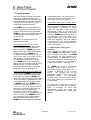
CC1000 is configured via a simple 3-wire
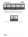
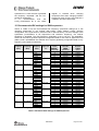
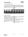
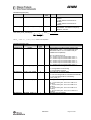
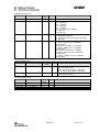
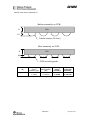
The timing for the programming is also
shown in Figure 4 with reference to Table
2. The clocking of the data on PDATA is
done on the negative edge of PCLK.
When the last bit, D0, of the 8 data-bits
has been loaded, the data word is loaded
in the internal configuration register.
interface (PDATA, PCLK and PALE).
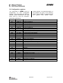
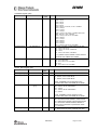
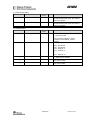
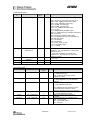
There are 28 8-bit configuration registers,
each addressed by a 7-bit address. A
Read/Write bit initiates a read or write
operation. A full configuration of CC1000
requires sending 22 data frames of 16 bits
each (7 address bits, R/W bit and 8 data
bits). The time needed for a full
configuration depend on the PCLK
frequency. With a PCLK frequency of 10
MHz the full configuration is done in less
than 46 µs. Setting the device in power
down mode requires sending one frame
only and will in this case take less than 2
µs. All registers are also readable.
The configuration data is stored in internal
RAM. The data is retained during powerdown mode, but not when the powersupply is turned off. The registers can be
programmed in any order.
The configuration registers can also be
read by the microcontroller via the same
configuration interface. The seven address
bits are sent first, then the R/W bit set low
to initiate the data read-back. CC1000 then
returns the data from the addressed
register. PDATA is in this case used as an
output and must be tri-stated (or set high n
the case of an open collector pin) by the
microcontroller during the data read-back
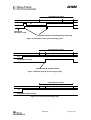
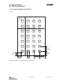
(D7:0). The read operation is illustrated in
Figure 5.
In each write-cycle 16 bits are sent on the
PDATA-line. The seven most significant
bits of each data frame (A6:0) are the
address-bits. A6 is the MSB (Most
Significant Bit) of the address and is sent
as the first bit. The next bit is the R/W bit
(high for write, low for read). During
address and R/W bit transfer the PALE
(Program Address Latch Enable) must be
kept low. The 8 data-bits are then
transferred (D7:0). See Figure 4.
TSA
THA
TCH,min
TCL,min
TSA
THD
TSD
PCLK
Address
PDATA
6
5
4
Write mode
3
2
1
0
W
Data byte
7
6
5
4
3
2
1
0
PALE
Figure 4. Configuration registers write operation
SWRS048A
Page 13 of 55