1
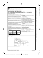
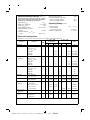
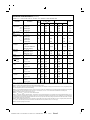
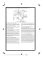
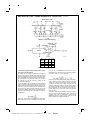
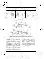
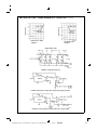
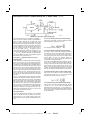
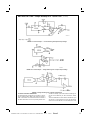
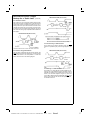
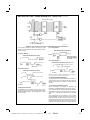
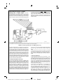
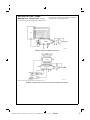
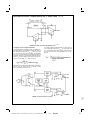
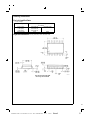
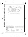
DAC1006,DAC1007,DAC1008
DAC1006/DAC1007/DAC1008 P Compatible, Double-Buffered D to A Converters
Literature Number: SNAS540
General Description
The DAC1006/7/8 are advanced CMOS/Si-Cr 10-, 9- and
8-bit accurate multiplying DACs which are designed to interface directly with the 8080, 8048, 8085, Z-80 and other
popular microprocessors. These DACs appear as a memory
location or an I/O port to the µP and no interfacing logic is
needed.
These devices, combined with an external amplifier and voltage reference, can be used as standard D/A converters; and
they are very attractive for multiplying applications (such as
digitally controlled gain blocks) since their linearity error is
essentially independent of the voltage reference. They become equally attractive in audio signal processing equipment as audio gain controls or as programmable attenuators
which marry high quality audio signal processing to digitally
based systems under microprocessor control.
All of these DACs are double buffered. They can load all 10
bits or two 8-bit bytes and the data format is left justified. The
analog section of these DACs is essentially the same as that
of the DAC1020.
The DAC1006 series are the 10-bit members of a family of
microprocessor-compatible DAC’s (MICRO-DAC’s™). For
applications requiring other resolutions, the DAC0830 series
(8 bits) and the DAC1208 and DAC1230 (12 bits) are available alternatives.
Part #
Accuracy
Pin
Description
(bits)
DAC1006
10
DAC1007
9
DAC1008
8
Features
n Uses easy to adjust END POINT specs, NOT BEST
STRAIGHT LINE FIT
n Low power consumption
n Direct interface to all popular microprocessors
n Integrated thin film on CMOS structure
n Double-buffered, single-buffered or flow through digital
data inputs
n Loads two 8-bit bytes or a single 10-bit word
n Logic inputs which meet TTL voltage level specs (1.4V
logic threshold)
n Works with ± 10V reference — full 4-quadrant
multiplication
n Operates STAND ALONE (without µP) if desired
n Available in 0.3" standard 20-pin package
n Differential non-linearity selection available as special
order
Key Specifications
n
n
n
n
n
n
Output Current Settling Time: 500 ns
Resolution: 10 bits
Linearity: 10, 9, and 8 bits (guaranteed over temp.)
Gain Tempco: −0.0003% of FS/˚C
Low Power Dissipation: 20 mW (including ladder)
Single Power Supply: 5 to 15 VDC
For left20
justified
data
Typical Application
DAC1006/1007/1008
DAC1006/DAC1007/DAC1008
DAC1006/DAC1007/DAC1008
µP Compatible, Double-Buffered D to A Converters
DAC1006/DAC1007/DAC1008 µP Compatible, Double-Buffered D to A Converters
April 1998
DS005688-1
*NOTE: FOR DETAILS OF BUS CONNECTION SEE SECTION 6.0
MICRO-DAC™ and BI-FET™ are trademarks of National Semiconductor Corp.
© 1998 National Semiconductor Corporation
DS005688
PrintDate=1998/11/17 PrintTime=11:38:07 46711 ds005688 Rev. No. 4
www.national.com
cmserv
Proof
1
1
Absolute Maximum Ratings (Notes 1, 2)
ESD Susceptibility (Note 11)
Lead Temp. (Soldering, 10 seconds)
Dual-In-Line Package (plastic)
Dual-In-Line Package (ceramic)
If Military/Aerospace specified devices are required,
please contact the National Semiconductor Sales Office/
Distributors for availability and specifications.
Supply Voltage (VCC)
Voltage at Any Digital Input
Voltage at VREF Input
Storage Temperature Range
Package Dissipation at TA = 25˚C
(Note 3)
DC Voltage Applied to IOUT1 or IOUT2
(Note 4)
17 VDC
VCC to GND
± 25V
−65˚C to +150˚C
Operating Ratings
800V
260˚C
300˚C
(Note 1)
TMIN ≤ TA ≤ TMAX
Temperature Range
Part numbers with
“LCN” and “LCWN” suffix
Voltage at Any Digital Input
500 mW
0˚C to 70˚C
VCC to GND
−100 mV to VCC
Electrical Characteristics
Tested at VCC = 4.75 VDC and 15.75 VDC, TA = 25˚C, VREF = 10.000 VDC unless otherwise noted
Parameter
Conditions
VCC = 12VDC ± 5%
See
Note
Min.
Typ.
Resolution
Linearity Error
Differential
Nonlinearity
Monotonicity
Min.
Typ.
Max.
10
bits
DAC1006
0.05
0.05
% of FSR
DAC1007
0.1
0.1
% of FSR
DAC1008
0.2
0.2
% of FSR
DAC1006
0.1
0.1
% of FSR
DAC1007
0.2
0.2
% of FSR
DAC1008
0.4
0.4
% of FSR
4,7
TMIN < TA < TMAX
6
−10V≤VREF≤+10V
5
Endpoint adjust only
4,7
TMIN < TA < TMAX
6
−10V≤VREF≤+10V
5
TMIN < TA < TMAX
4,6
5
DAC1006
10
10
bits
DAC1007
9
9
bits
DAC1008
8
8
bits
Gain Error
Using internal Rfb
−10V≤VREF≤+10V
5
Gain Error Tempco
TMIN < TA < TMAX
6
Using internal Rfb
9
Rejection
Units
Max.
10
Endpoint adjust only
−10V≤VREF≤+10V
Power Supply
VCC = 5VDC ± 5%
to 15VDC ± 5%
± 0.3
1.0
−0.0003
−0.001
VCC = 14.5V to 15.5V
0.003
0.008
11.5V to 12.5V
0.004
0.010
−1.0
−1.0
± 0.3
1.0
% of FS
−0.0006
−0.002
% of FS/˚C
All digital inputs
latched high
% FSR/V
% FSR/V
4.75V to 5.25V
0.033
0.10
% FSR/V
15
20
kΩ
Reference Input
Resistance
Output Feedthrough
Error
10
15
20
10
VREF = 20Vp-p, f = 100 kHz
All data inputs
90
90
mVp-p
latched low
www.national.com
2
PrintDate=1998/11/17 PrintTime=11:38:07 46711 ds005688 Rev. No. 4
cmserv
Proof
2
Electrical Characteristics
(Continued)
= 4.75 VDC and 15.75 VDC, TA = 25˚C, VREF = 10.000 VDC unless otherwise noted
Tested at VCC
Parameter
Conditions
VCC = 12VDC ± 5%
See
Note
Min.
Output
IOUT1
Capacitance IOUT2
All data inputs
latched low
Typ.
Min.
Typ.
Max.
60
60
pF
250
250
pF
All data inputs
250
250
pF
IOUT2
latched high
60
60
pF
Output Leakage
TMIN≤TA≤TMAX
6
TMIN≤TA≤TMAX
6
IOUT1
All data inputs
IOUT2
All data inputs
latched low
0.5
10
latched high
TMIN≤TA≤TMAX
Digital Input
Voltages
3.5
0.5
3.5
mA
200
200
nA
200
200
nA
0.7, 0.8
VDC
6
Low level
LCN and LCWM suffix
0.8, 0.8
High level (all parts)
TMIN≤TA≤TMAX
Digital Input
Currents
Current
Units
Max.
IOUT1
Supply Current
Drain
Current
VCC = 5VDC ± 5%
to 15VDC ± 5%
tS
2.0
2.0
VDC
6
Digital inputs < 0.8V
−40
−150
−40
−150
µADC
Digital inputs > 2.0V
VIL = 0V, VIH = 5V
1.0
+10
1.0
+10
µADC
500
500
ns
Settling Time
Write and
tW
XFER Pulse
Width
Data Set Up
tDS
Time
Data Hold
tDH
tCS
Time
tCH
8
150
60
320
200
ns
9
320
100
500
250
ns
9
TMIN≤TA≤TMAX
VIL = OV, VIH = 5V
9
TMIN≤TA≤TMAX
VIL = 0V, VIL = 5V,
TA = 25˚C
Up Time
Control Hold
TMIN≤TA≤TMAX
VIL = 0V, VIH = 5V,
TA = 25˚C
TA = 25˚C
Time
Control Set
VIL = 0V, VIH = 5V,
TA = 25˚C
9
TMIN≤TA≤TMAX
VIL = 0V, VIH = 5V,
TA = 25˚C
TMIN≤TA≤TMAX
9
150
80
320
170
ns
320
120
500
250
ns
200
100
320
220
ns
250
120
500
320
ns
150
60
320
180
ns
320
100
500
260
ns
10
0
10
0
ns
10
0
10
0
ns
Note 1: Absolute Maximum Ratings indicate limits beyond which damage to the device may occur. DC and AC electrical specifications do not apply when operating
the device beyond its specified operating conditions.
Note 2: All voltages are measured with respect to GND, unless otherwise specified.
Note 3: This 500 mW specification applies for all packages. The low intrinsic power dissipation of this part (and the fact that there is no way to significantly modify
the power dissipation) removes concern for heat sinking.
Note 4: For current switching applications, both IOUT1 and IOUT2 must go to ground or the “Virtual Ground” of an operational amplifier. The linearity error is degraded
by approximately VOS÷VREF. For example, if VREF = 10V then a 1 mV offset, VOS, on IOUT1 or IOUT2 will introduce an additional 0.01% linearity error.
Note 5: Guaranteed at VREF = ± 10 VDC and VREF = ± 1 VDC.
Note 6: TMIN = 0˚C and TMAX = 70˚C for “LCN” and “LCWM” suffix parts.
Note 7: The unit “FSR” stands for “Full Scale Range.” “Linearity Error” and “Power Supply Rejection” specs are based on this unit to eliminate dependence on a particular VREF value and to indicate the true performance of the part. The “Linearity Error” specification of the DAC1006 is “0.05% of FSR (MAX).” This guarantees that
after performing a zero and full scale adjustment (See Sections 2.5 and 2.6), the plot of the 1024 analog voltage outputs will each be within 0.05%xVREF of a straight
line which passes through zero and full scale.
Note 8: This specification implies that all parts are guaranteed to operate with a write pulse or transfer pulse width (tW) of 320 ns. A typical part will operate with tW
of only 100 ns. The entire write pulse must occur within the valid data interval for the specified tW, tDS, tDH, and tS to apply.
Note 9: Guaranteed by design but not tested.
3
PrintDate=1998/11/17 PrintTime=11:38:08 46711 ds005688 Rev. No. 4
www.national.com
cmserv
Proof
3
Electrical Characteristics
(Continued)
Note 10: A 200 nA leakage current with Rfb = 20K and VREF = 10V corresponds to a zero error of (200x10−9x20x103)x100÷ 10 which is 0.04% of FS.
Note 11: Human body model, 100 pF discharged through a 1.5 kΩ resistor.
Switching Waveforms
DS005688-2
www.national.com
4
PrintDate=1998/11/17 PrintTime=11:38:08 46711 ds005688 Rev. No. 4
cmserv
Proof
4
Typical Performance Characteristics
Errors vs. Supply Voltage
Write Width, tw
Errors vs. Temperature
DS005688-31
DS005688-30
DS005688-29
Control Setup Time, tCS
Data Setup Time, tDS
DS005688-32
Data Hold Time, tDH
DS005688-34
DS005688-33
Digital Threshold
vs. Supply Voltage
Digital Input Threshold
vs. Temperature
DS005688-35
DS005688-36
5
PrintDate=1998/11/17 PrintTime=11:38:08 46711 ds005688 Rev. No. 4
www.national.com
cmserv
Proof
5
Block and Connection Diagrams
DAC1006/1007/1008 (20-Pin Parts)
DS005688-5
Use DAC1006/1007/1008 for left justified data.
DAC1006/1007/1008
(20-Pin Parts)
Dual-In-Line Package
DS005688-28
Top View
See Ordering Information
www.national.com
6
PrintDate=1998/11/17 PrintTime=11:38:08 46711 ds005688 Rev. No. 4
cmserv
Proof
6
DAC1006/1007/1008 — Simple Hookup for a “Quick Look”
DS005688-7
*A TOTAL OF 10 INPUT SWITCHES & 1K RESISTORS
Notes:
1. For VREF = −10.240 VDC the output voltage steps are approximately 10 mV each.
2. SW1 is a normally closed switch. While SW1 is closed, the DAC register is latched and new data can be loaded into the input latch via the 10 SW2 switches.
When SW1 is momentarily opened the new data is transferred from the input latch to the DAC register and is latched when SW1 again closes.
amp is used to provide an output voltage for the DAC. This
on-chip resistor should always be used (not an external resistor) because it matches the resistors used in the on-chip
R-2R ladder and tracks these resistors over temperature.
VREF: Reference Voltage Input — This is the connection for
the external precision voltage source which drives the R-2R
ladder. VREF can range from −10 to +10 volts. This is also the
analog voltage input for a 4-quadrant multiplying DAC application.
VCC: Digital Supply Voltage — This is the power supply pin
for the part. VCC can be from +5 to +15 VDC. Operation is optimum for +15V. The input threshold voltages are nearly independent of VCC. (See Typical Performance Characteristics
and Description in Section 3.0, T2L compatible logic inputs.)
GND: Ground — the ground pin for the part.
1.3 Definition of Terms
Resolution: Resolution is directly related to the number of
switches or bits within the DAC. For example, the DAC1006
has 210 or 1024 steps and therefore has 10-bit resolution.
Linearity Error: Linearity error is the maximum deviation
from a straight line passing through the endpoints of the
DAC transfer characteristic. It is measured after adjusting for
zero and full-scale. Linearity error is a parameter intrinsic to
the device and cannot be externally adjusted.
National’s linearity test (a) and the “best straight line” test (b)
used by other suppliers are illustrated below. The “best
straight line” requires a special zero and FS adjustment for
each part, which is almost impossible for user to determine.
The “end point test” uses a standard zero and FS adjustment
procedure and is a much more stringent test for DAC linearity.
Power Supply Sensitivity: Power supply sensitivity is a
measure of the effect of power supply changes on the DAC
full-scale output (which is the worst case).
1.0 DEFINITION OF PACKAGE PINOUTS
1.1 Control Signals (All control signals are level actuated.)
CS: Chip Select — active low, it will enable WR.
WR: Write — The active low WR is used to load the digital
data bits (DI) into the input latch. The data in the input latch
is latched when WR is high. The 10-bit input latch is split into
two latches; one holds 8 bits and the other holds 2 bits. The
Byte1/Byte2 control pin is used to select both input latches
when Byte1/Byte2 = 1 or to overwrite the 2-bit input latch
when in the low state.
Byte1/Byte2: Byte Sequence Control — When this control
is high, all ten locations of the input latch are enabled. When
low, only two locations of the input latch are enabled and
these two locations are overwritten on the second byte write.
On the DAC1006, 1007, and 1008, the Byte1/Byte2 must be
low to transfer the 10-bit data in the input latch to the DAC
register.
XFER: Transfer Control Signal, active low — This signal, in
combination with others, is used to transfer the 10-bit data
which is available in the input latch to the DAC register —
see timing diagrams.
1.2 Other Pin Functions
DIi (i = 0 to 9): Digital Inputs — DI0 is the least significant bit
(LSB) and DIg is the most significant bit (MSB).
IOUT1: DAC Current Output 1 — IOUT1 is a maximum for a
digital input code of all 1s and is zero for a digital input code
of all 0s.
IOUT2: DAC Current Output 2 — IOUT2 is a constant minus
IOUT1, or
where R ≅ 15 kΩ.
RFB: Feedback Resistor — This is provided on the IC chip
for use as the shunt feedback resistor when an external op
7
PrintDate=1998/11/17 PrintTime=11:38:08 46711 ds005688 Rev. No. 4
www.national.com
cmserv
Proof
7
DAC1006/1007/1008 — Simple Hookup for a “Quick Look”
a. End Point Test After Zero and FS Adj.
(Continued)
b. Best Straight Line
DS005688-37
DS005688-38
3.0 TTL COMPATIBLE LOGIC INPUTS
Settling Time: Settling time is the time required from a code
transition until the DAC output reaches within ± 1⁄2 LSB of the
final output value. Full-scale settling time requires a zero to
full-scale or full-scale to zero output change.
Full-Scale Error: Full scale error is a measure of the output
error between an ideal DAC and the actual device output.
Ideally, for the DAC1006 series, full-scale is VREF−1 LSB.
For
VREF = −10V
and
unipolar
operation,
VFULL-SCALE = 10.0000V −9.8mV = 9.9902V. Full-scale error is
adjustable to zero.
Monotonicity: If the output of a DAC increases for increasing digital input code, then the DAC is monotonic. A 10-bit
DAC with 10-bit monotonicity will produce an increasing analog output when all 10 digital inputs are exercised. A 10-bit
DAC with 9-bit monotonicity will be monotonic when only the
most significant 9 bits are exercised. Similarly, 8-bit monotonicity is guaranteed when only the most significant 8 bits are
exercised.
To guarantee TTL voltage compatibility of the logic inputs, a
novel bipolar (NPN) regulator circuit is used. This makes the
input logic thresholds equal to the forward drop of two diodes
(and also matches the temperature variation) as occurs
naturally in TTL. The basic circuit is shown in Figure 1. A
curve of digital input threshold as a function of power supply
voltage is shown in the Typical Performance Characteristics
section.
4.0 APPLICATION HINTS
The DC stability of the VREF source is the most important
factor to maintain accuracy of the DAC over time and temperature changes. A good single point ground for the analog
signals is next in importance.
These MICRO-DAC converters are CMOS products and reasonable care should be exercised in handling them prior to final mounting on a PC board. The digital inputs are protected,
but permanent damage may occur if the part is subjected to
high electrostatic fields. Store unused parts in conductive
foam or anti-static rails.
2.0 DOUBLE BUFFERING
These DACs are double-buffered, microprocessor compatible versions of the DAC1020 10-bit multiplying DAC. The
addition of the buffers for the digital input data not only allows for storage of this data, but also provides a way to assemble the 10-bit input data word from two write cycles when
using an 8-bit data bus. Thus, the next data update for the
DAC output can be made with the complete new set of 10-bit
data. Further, the double buffering allows many DACs in a
system to store current data and also the next data. The updating of the new data for each DAC is also not time critical.
When all DACs are updated, a common strobe signal can
then be used to cause all DACs to switch to their new analog
output levels.
www.national.com
4.1 Power Supply Sequencing & Decoupling
Some IC amplifiers draw excessive current from the Analog
inputs to V− when the supplies are first turned on. To prevent
damage to the DAC — an external Schottky diode connected from IOUT1 or IOUT2 to ground may be required to prevent destructive currents in IOUT1 or IOUT2. If an LM741 or
LF356 is used — these diodes are not required.
The standard power supply decoupling capacitors which are
used for the op amp are adequate for the DAC.
8
PrintDate=1998/11/17 PrintTime=11:38:08 46711 ds005688 Rev. No. 4
cmserv
Proof
8
DAC1006/1007/1008 — Simple Hookup for a “Quick Look”
(Continued)
DS005688-9
FIGURE 1. Basic Logic Threshold Loop
der current to the IOUT1 output pin. These MOS switches operate in the current mode with a small voltage drop across
them and can therefore switch currents of either polarity.
This is the basis for the 4-quadrant multiplying feature of this
DAC.
4.2 Op Amp Bias Current & Input Leads
The op amp bias current (IB) CAN CAUSE DC ERRORS.
BI-FET™ op amps have very low bias current, and therefore
the error introduced is negligible. BI-FET op amps are
strongly recommended for these DACs.
The distance from the IOUT1 pin of the DAC to the inverting
input of the op amp should be kept as short as possible to
prevent inadvertent noise pickup.
5.1.1 Providing a Unipolar Output Voltage with the
DAC in the Current Switching Mode
A voltage output is provided by making use of an external op
amp as a current-to-voltage converter. The idea is to use the
internal feedback resistor, RFB, from the output of the op
amp to the inverting (−) input. Now, when current is entered
at this inverting input, the feedback action of the op amp
keeps that input at ground potential. This causes the applied
input current to be diverted to the feedback resistor. The output voltage of the op amp is forced to a voltage given by:
VOUT = −(IOUT1xRFB)
5.0 ANALOG APPLICATIONS
The analog section of these DACs uses an R-2R ladder
which can be operated both in the current switching mode
and in the voltage switching mode.
The major product changes (compared with the DAC1020)
have been made in the digital functioning of the DAC. The
analog functioning is reviewed here for completeness. For
additional analog applications, such as multipliers, attenuators, digitally controlled amplifiers and low frequency sine
wave oscillators, refer to the DAC1020 data sheet. Some basic circuit ideas are presented in this section in addition to
complete applications circuits.
Notice that the sign of the output voltage depends on the direction of current flow through the feedback resistor.
In current switching mode applications, both current output
pins (IOUT1 and IOUT2) should be operated at 0 VDC. This is
accomplished as shown in Figure 3. The capacitor, CC, is
used to compensate for the output capacitance of the DAC
and the input capacitance of the op amp. The required feedback resistor, RFB, is available on the chip (one end is internally tied to IOUT1) and must be used since an external resistor will not provide the needed matching and temperature
tracking. This circuit can therefore be simplified as shown in
Figure 4, where the sign of the reference voltage has been
changed to provide a positive output voltage. Note that the
output current, IOUT1, now flows through the RFB pin.
5.1 Operation in Current Switching Mode
The analog circuitry, Figure 2, consists of a silicon-chromium
(Si-Cr) thin film R-2R ladder which is deposited on the surface oxide of the monolithic chip. As a result, there is no
parasitic diode connected to the VREF pin as would exist if
diffused resistors were used. The reference voltage input
(VREF) can therefore range from −10V to +10V.
The digital input code to the DAC simply controls the position
of the SPDT current switches, SW0 to SW9. A logical 1 digital input causes the current switch to steer the available lad-
9
PrintDate=1998/11/17 PrintTime=11:38:09 46711 ds005688 Rev. No. 4
www.national.com
cmserv
Proof
9
DAC1006/1007/1008 — Simple Hookup for a “Quick Look”
(Continued)
DIGITAL INPUT CODE
DS005688-39
FIGURE 2. Current Mode Switching
DS005688-40
OP
AMP
CC
pF
Rj
ts µS
LF356
22
24
∞
∞
3
LF351
LF357
10
2.4k
1.5
4
FIGURE 3. Converting IOUT to VOUT
(−512≤D≤+511 or 1000000000≤D≤0111111111). If the applied digital input is interpreted as the decimal equivalent of
a true binary word, VOUT can be found by:
5.1.2 Providing a Bipolar Output Voltage with the DAC
in the Current Switching Mode
The addition of a second op amp to the circuit of Figure 4
can be used to generate a bipolar output voltage from a fixed
reference voltage Figure 5. This, in effect, gives sign significance to the MSB of the digital input word to allow two quadrant multiplication of the reference voltage. The polarity of
the reference can also be reversed to realize the full
four-quadrant multiplication.
The applied digital word is offset binary which includes a
code to output zero volts without the need of a large valued
resistor common to existing bipolar multiplying DAC circuits.
Offset binary code can be derived from 2’s complement data
(most common for signed processor arithmetic) by inverting
the state of the MSB in either software or hardware. After doing this the output then responds in accordance to the following expression:
With this configuration, only the offset voltage of amplifier 1
need be nulled to preserve linearity of the DAC. The offset
voltage error of the second op amp has no effect on linearity.
It presents a constant output voltage error and should be
nulled only if absolute accuracy is needed. Another advantage of this configuration is that the values of the external resistors required do not have to match the value of the internal DAC resistors; they need only to match and temperature
track each other.
A thin film 4 resistor network available from Beckman Instruments, Inc. (part no. 694-3-R10K-D) is ideally suited for this
application. Two of the four available 10 kΩ resistor can be
paralleled to form R in Figure 5 and the other two can be
used separately as the resistors labeled 2R.
where VREF can be positive or negative and D is the signed
decimal equivalent of the 2’s complement processor data.
www.national.com
10
PrintDate=1998/11/17 PrintTime=11:38:09 46711 ds005688 Rev. No. 4
cmserv
Proof
10
DAC1006/1007/1008 — Simple Hookup for a “Quick Look”
(Continued)
Operation is summarized in the table below:
Applied
2’s Comp.
2’s Comp.
Applied
True Binary
(Decimal)
(Binary)
Digital Input
(Decimal)
+VREF
−VREF
0111111111
1111111111
1023
VREF−1 LSB
−|VREF|+1 LSB
−|VREF|/2
+511
VOUT
+256
0100000000
1100000000
768
VREF/2
0
0000000000
1000000000
512
0
0
−1
1111111111
0111111111
511
−1 LSB
+1 LSB
−256
1100000000
0100000000
256
−VREF/2
+|VREF|/2
−512
1000000000
0000000000
0
−VREF
+|VREF|
DS005688-41
FIGURE 4. Providing a Unipolar Output Voltage
DS005688-42
FIGURE 5. Providing a Bipolar Output Voltage with the DAC in the Current Switching Mode
single op amp as shown in Figure 10. For a digital input code
of all zeros, the output voltage from the VREF pin is zero
volts. The external op amp now has a single input of +V and
is operating with a gain of −1 to this input. The output of the
op amp therefore will be at −V for a digital input of all zeros.
As the digital code increases, the output voltage at the VREF
pin increases.
Notice that the gain of the op amp to voltages which are applied to the (+) input is +2 and the gain to voltages which are
applied to the input resistor, R, is −1. The output voltage of
the op amp depends on both of these inputs and is given by:
VOUT = (+V) (−1)+VREF(+2)
5.2 Analog Operation in the Voltage Switching Mode
Some useful application circuits result if the R-2R ladder is
operated in the voltage switching mode. There are two very
important things to remember when using the DAC in the
voltage mode. The reference voltage (+V) must always be
positive since there are parasitic diodes to ground on the
IOUT1 pin which would turn on if the reference voltage went
negative. To maintain a degradation of linearity less than
± 0.005%, keep +V ≤ 3 VDC and VCC at least 10V more positive than +V. Figures 6, 7 show these errors for the voltage
switching mode. This operation appears unusual, since a reference voltage (+V) is applied to the IOUT1 pin and the voltage output is the VREF pin. This basic idea is shown in Figure
8.
This VOUT range can be scaled by use of a non-inverting
gain stage as shown in Figure 9.
Notice that this is unipolar operation since all voltages are
positive. A bipolar output voltage can be obtained by using a
11
PrintDate=1998/11/17 PrintTime=11:38:09 46711 ds005688 Rev. No. 4
www.national.com
cmserv
Proof
11
DAC1006/1007/1008 — Simple Hookup for a “Quick Look”
(Continued)
DS005688-43
DS005688-44
FIGURE 6.
FIGURE 7.
DIGITAL INPUT CODE
DS005688-45
FIGURE 8. Voltage Mode Switching
DS005688-46
FIGURE 9. Amplifying the Voltage Mode Output (Single Supply Operation)
DS005688-47
FIGURE 10. Providing a Bipolar Output Voltage with a Single Op Amp
www.national.com
12
PrintDate=1998/11/17 PrintTime=11:38:09 46711 ds005688 Rev. No. 4
cmserv
Proof
12
DAC1006/1007/1008 — Simple Hookup for a “Quick Look”
(Continued)
DS005688-48
FIGURE 11. Increasing the Output Voltage Swing
5.4.1 Current Switching with Unipolar Output Voltage
After doing a “zero adjust,” set all of the digital input levels
HIGH and adjust the magnitude of VREF for
The output voltage swing can be expanded by adding 2 resistors to Figure 10 as shown in Figure 11. These added resistors are used to attenuate the +V voltage. The overall
gain, AV(−), from the +V terminal to the output of the op amp
determines the most negative output voltage, −4(+V) (when
the VREF voltage at the + input of the op amp is zero) with the
component values shown. The complete dynamic range of
VOUT is provided by the gain from the (+) input of the op
amp. As the voltage at the VREF pin ranges from 0V to
+V(1023/1024) the output of the op amp will range from −10
VDC to +10V (1023/1024) when using a +V voltage of +2.500
VDC. The 2.5 VDC reference voltage can be easily developed
by using the LM336 zener which can be biased through the
RFB internal resistor, connected to VCC.
This completes the DAC calibration.
5.4.2 Current Switching with Bipolar Output Voltage
The circuit of Figure 12 shows the 3 adjustments needed.
The first step is to set all of the digital inputs LOW (to force
IOUT1 to 0) and then trim “zero adj.” for zero volts at the inverting input (pin 2) of 0A1. Next, with a code of all zeros still
applied, adjust “−FS adj.”, the reference voltage, for
VOUT = ± |(ideal VREF)|. The sign of the output voltage will be
opposite that of the applied reference.
Finally, set all of the digital inputs HIGH and adjust “+FS adj.”
for VOUT = VREF (511/512). The sign of the output at this time
will be the same as that of the reference voltage. The addition of the 200Ω resistor in series with the VREF pin of the
DAC is to force the circuit gain error from the DAC to be
negative. This insures that adding resistance to Rfb, with the
500Ω pot, will always compensate the gain error of the DAC.
5.3 Op Amp VOS Adjust (Zero Adjust) for Current
Switching Mode
Proper operation of the ladder requires that all of the 2R legs
always go to exactly 0 VDC (ground). Therefore offset voltage, VOS, of the external op amp cannot be tolerated as every millivolt of VOS will introduce 0.01% of added linearity error. At first this seems unusually sensitive, until it becomes
clear the 1 mV is 0.01% of the 10V reference! High resolution converters of high accuracy require attention to every
detail in an application to achieve the available performance
which is inherent in the part. To prevent this source of error,
the VOS of the op amp has to be initially zeroed. This is the
“zero adjust” of the DAC calibration sequence and should be
done first.
If the VOS is to be adjusted there are a few points to consider.
Note that no “dc balancing” resistance should be used in the
grounded positive input lead of the op amp. This resistance
and the input current of the op amp can also create errors.
The low input biasing current of the BI-FET op amps makes
them ideal for use in DAC current to voltage applications.
The VOS of the op amp should be adjusted with a digital input
of all zeros to force IOUT = 0 mA. A 1 kΩ resistor can be temporarily connected from the inverting input to ground to provide a dc gain of approximately 15 to the VOS of the op amp
and make the zeroing easier to sense.
5.4.3 Voltage Switching with a Unipolar Output Voltage
Refer to the circuit of Figure 13 and set all digital inputs
LOW. Trim the “zero adj.” for VOUT = 0 VDC ± 1 mV. Then set
all digital inputs HIGH and trim the “FS Adj.” for:
5.4.4 Voltage Switching with a Bipolar Output Voltage
Refer to Figure 14 and set all digital inputs LOW. Trim the
“−FS Adj.” for VOUT = −2.5 VDC. Then set all digital inputs
HIGH and trim the “+FS Adj.” for VOUT = +2.5 (511/512) VDC.
Test the zero by setting the MS digital input HIGH and all the
rest LOW. Adjust VOS of amp #3, if necessary, and recheck
the full-scale values.
5.4 Full-Scale Adjust
The full-scale adjust procedure depends on the application
circuit and whether the DAC is operated in the current
switching mode or in the voltage switching mode. Techniques are given below for all of the possible application circuits.
13
PrintDate=1998/11/17 PrintTime=11:38:09 46711 ds005688 Rev. No. 4
www.national.com
cmserv
Proof
13
DAC1006/1007/1008 — Simple Hookup for a “Quick Look”
(Continued)
DS005688-49
FIGURE 12. Full Scale Adjust — Current Switching with Bipolar Output Voltage
DS005688-50
FIGURE 13. Full Scale Adjust — Voltage Switching with a Unipolar Output Voltage
DS005688-15
FIGURE 14. Voltage Switching with a Bipolar Output Voltage
cussed. For example, if your main interest in interfacing to a
µP with an 8-bit data bus you will be directed to Section
6.1.0.
The first consideration is “will the DAC be interfaced to a µP
with an 8-bit or a 16-bit data bus or used in the stand-alone
mode?” For the 8-bit data bus, a second selection is made
6.0 DIGITAL CONTROL DESCRIPTION
The DAC1006 series of products can be used in a wide variety of operating modes. Most of the options are shown in
Table 1. Also shown in this table are the section numbers of
this data sheet where each of the operating modes is dis-
www.national.com
14
PrintDate=1998/11/17 PrintTime=11:38:09 46711 ds005688 Rev. No. 4
cmserv
Proof
14
DAC1006/1007/1008 — Simple
Hookup for a “Quick Look” (Continued)
buffer, 2) using both digital data buffers — “double buffered,” or 3) allowing the input digital data to “flow through” to
provide the analog output without the use of any data
latches.
on how the 2nd digital data buffer (the DAC Latch) is updated by a transfer from the 1st digital data buffer (the Input
Latch). Three options are provided: 1) an automatic transfer
when the 2nd data byte is written to the DAC, 2) a transfer
which is under the control of the µP and can include more
than one DAC in a simultaneous transfer, or 3) a transfer
which is under the control of external logic. Further, the data
format can be either left justified or right justified.
When interfacing to a µP with a 16-bit data bus only two selections are available: 1) operating the DAC with a single
digital data buffer (the transfer of one DAC does not have to
be synchronized with any other DACs in the system), or 2)
operating with a double digital data buffer for simultaneous
transfer, or updating, of more than one DAC.
For operating without a µP in the stand alone mode, three
options are provided: 1) using only a single digital data
To reduce the required reading, only the applicable sections
of 6.1 through 6.4 need be considered.
6.1 Interfacing to an 8-Bit Data Bus
Transferring 10 bits of data over an 8-bit bus requires two
write cycles and provides four possible combinations which
depend upon two basic data format and protocol decisions:
1. Is the data to be left justified (considered as fractional binary data with the binary point to the left) or right justified
(considered as binary weighted data with the binary
point to the right)?
2. Which byte will be transfered first, the most significant
byte (MS byte) or the least significant byte (LS byte)?
TABLE 1.
Operating Mode
Automatic Transfer
µP Control Transfer
External Transfer
Section
Figure No.
Section
Figure No.
Section
Figure No.
6.2.1
16
6.2.2
16
6.2.3
16
Data Bus
8-Bit Data Bus (6.1.0)
Left Justified (6.1.1)
16-Bit Data Bus (6.3.0)
Single Buffered
6.3.1
Stand Alone (6.4.0)
Double Buffered
17
6.3.2
Single Buffered
6.4.1
17
17
Not Applicable
Double Buffered
Flow Through
6.4.2
These data possibilities are shown in Figure 15. Note that
the justification of data depends on how the 10-bit data word
is located within the 16-bit data source (CPU) register. In either case, there is a surplus of 6 bits and these are shown as
“don’t care” terms (“x”) in this figure.
All of these DACs load 10 bits on the 1st write cycle. A particular set of 2 bits is then overwritten on the 2nd write cycle,
depending on the justification of the data. For all left justified
data options, the 1st write cycle must contain the MS or Hi
Byte data group.
Flow Through
17
NA
6.2 Controlling Data Transfer for an 8-Bit Data Bus
Three operating modes are possible for controlling the transfer of data from the Input Latch to the DAC Register, where
it will update the analog output voltage. The simplest is the
automatic transfer mode, which causes the data transfer to
occur at the time of the 2nd write cycle. This is recommended when the exact timing of the changes of the DAC
analog output are not critical. This typically happens where
each DAC is operating individually in a system and the analog updating of one DAC is not required to be synchronized
to any other DAC. For synchronized DAC updating, two options are provided: µP control via a common XFER strobe or
external update timing control via an external strobe. The details of these options are now shown.
6.1.1 For Left Justified Data
For applications which require left justified data,
DAC1006–1008 can be used. A simplified logic diagram
which shows the external connections to the data bus and
the internal functions of both of the data buffer registers (Input Latch and DAC Register) is shown in Figure 16. These
parts require the MS or Hi Byte data group to be transferred
on the 1st write cycle.
15
PrintDate=1998/11/17 PrintTime=11:38:10 46711 ds005688 Rev. No. 4
www.national.com
cmserv
Proof
15
DAC1006/1007/1008 — Simple Hookup for a “Quick Look”
(Continued)
DAC1006/1007/1008 (20-Pin Parts for Left Justified Data)
DS005688-16
FIGURE 15. Fitting a 10-Bit Data Word into 16 Available Bit Locations
DS005688-17
FIGURE 16. Input Connections and Controls for DAC1006/1007/1008 Left Justified Data
www.national.com
16
PrintDate=1998/11/17 PrintTime=11:38:10 46711 ds005688 Rev. No. 4
cmserv
Proof
16
DAC1006/1007/1008 — Simple
Hookup for a “Quick Look” (Continued)
DAC1006/1007/1008 (20–Pin Parts)
6.2.1 Automatic Transfer
This makes use of a double byte (double precision) write.
The first byte (8 bits) is strobed into the input latch and the
second byte causes a simultaneous strobe of the two remaining bits into the input latch and also the transfer of the
complete 10-bit word from the input latch to the DAC register. This is shown in the following timing diagram; the point in
time where the analog output is updated is also indicated on
this diagram.
DAC1006/1007/1008 (20-Pin Parts)
DS005688-19
6.2.3 Transfer Using an External Strobe
This is similar to the previous operation except the XFER
signal is not provided by the µP. The timing diagram for this
is:
DS005688-18
*SIGNIFIES CONTROL INPUTS WHICH ARE DRIVEN IN PARALLEL
DAC1006/1007/1008 (20–Pin Parts)
6.2.2 Transfer Using µP Write Stroke
The input latch is loaded with the first two write strobes. The
XFER signal is provided by external logic, as shown below,
to cause the transfer to be accomplished on a third write
strobe. This is shown in the following diagram:
DS005688-20
6.3 Interfacing to a 16-Bit Data Bus
The interface to a 16-bit data bus is easily handled by connecting to 10 of the available bus lines. This allows a wiring
selected right justified or left justified data format. This is
shown in the connection diagram of Figure 17, where the
use of DB6 to DB15 gives left justified data operation. Note
that any part number can be used and the Byte1/Byte2 control should be wired Hi.
17
PrintDate=1998/11/17 PrintTime=11:38:10 46711 ds005688 Rev. No. 4
www.national.com
cmserv
Proof
17
DAC1006/1007/1008 — Simple Hookup for a “Quick Look”
(Continued)
DS005688-21
FIGURE 17. Input Connections and Logic for DAC1006/1007/1008 with 16-Bit Data Bus
6.4.1 Single Buffered
Three operating modes are possible: flow through, single
buffered, or double buffered. The timing diagrams for these
are shown below:
DAC1006/1007/1008 (20-Pin Parts)
6.3.1 Single Buffered
DAC1006/1007/1008 (20-Pin Parts)
DS005688-53
6.4.2 Double Buffered
DAC1006/1007/1008 (20-Pin Parts) (Note 12)
DS005688-51
6.3.2 Double Buffered
DAC1006/1007/1008 (20-Pin Parts)
DS005688-54
Note 12: For a connection diagram of this operating mode use Figure 16 for
the Logic and Figure 17 for the Data Input connections.
7.0 MICROPROCESSOR INTERFACE
The logic functions of the DAC1006 family have been oriented towards an ease of interface with all popular µPs. The
following sections discuss in detail a few useful interface
schemes.
7.1 DAC1001/1/2 to INS8080A Interface
Figure 18 illustrates the simplicity of interfacing the
DAC1006 to an INS8080A based microprocessor system.
The circuit will perform an automatic transfer of the 10 bits of
output data from the CPU to the DAC register as outlined in
Section 6.2.1, “Controlling Data Transfer for an 8-Bit Data
Bus.”
DS005688-52
6.4 Stand Alone Operation
For applications for a DAC which are not under µP control
(stand alone) there are two basic operating modes, single
buffered and double buffered. The timing diagrams for these
are shown below:
Since a double byte write is necessary to control the DAC
with the INS8080A, a possible instruction to achieve this is a
PUSH of a register pair onto a “stack” in memory. The 16-bit
register pair word will contain the 10 bits of the eventual DAC
input data in the proper sequence to conform to both the requirements of the DAC (with regard to left justified data) and
www.national.com
18
PrintDate=1998/11/17 PrintTime=11:38:10 46711 ds005688 Rev. No. 4
cmserv
Proof
18
DAC1006/1007/1008 — Simple
Hookup for a “Quick Look” (Continued)
stack pointer during a PUSH allows using address bit 0 of
the stack pointer as the Byte1/Byte2 and XFER strobes if bit
0 of the stack pointer address −1, (SP−1), is a “1” as presented to the DAC. Additional address decoding by the
DM8131 will generate a unique DAC chip select (CS) and
synchronize this CS to the two memory write strobes of the
PUSH instruction.
the implementation of the PUSH instruction which will output
the higher order byte of the register pair (i.e., register B of the
BC pair) first. The DAC will actually appear as a two-byte
“stack” in memory to the CPU. The auto-decrementing of the
DS005688-24
NOTE: DOUBLE BYTE STORES CAN BE USED.
e.g. THE INSTRUCTION SHLD F001 STORES THE L REG INTO B1 AND THE H REG INTO B2 AND TRANSFERS THE RESULT TO THE DAC REGISTER.
THE OPERAND OF THE SHLD INSTRUCTION MUST BE AN ODD ADDRESS FOR PROPER TRANSFER.
FIGURE 18. Interfacing the DAC1000 to the INS8080A CPU Group
trol. The 10-bit data word in the DAC register will be latched
(and hence VOUT will be fixed) when CB2 is brought back
HIGH.
If both output ports of the PIA are not available, it is possible
to interface the DAC1006 through a single port without much
effort. However, additional logic at the CB2(or CA2) lines or
access to some of the 6800 system control lines will be required.
To reset the stack pointer so new data may be output to the
same DAC, a POP instruction followed by instructions to insure that proper data is in the DAC data register pair before
it is “PUSHED” to the DAC should be executed, as the POP
instruction will arbitrarily alter the contents of a register pair.
Another double byte write instruction is Store H and L Direct
(SHLD), where the HL register pair would temporarily contain the DAC data and the two sequential addresses for the
DAC are specified by the instruction op code. The auto incrementing of the DAC address by the SHLD instruction permits
the same simple scheme of using address bit 0 to generate
the byte number and transfer strobes.
7.3 Noise Considerations
A typical digital/microprocessor bus environment is a tremendous potential source of high frequency noise which can
be coupled to sensitive analog circuitry. The fast edges of the
data and address bus signals generate frequency components of 10’s of megahertz and can cause noise spikes to
appear at the DAC output. These noise spikes occur when
the data bus changes state or when data is transferred between the latches of the device.
In low frequency or DC applications, low pass filtering can
reduce these noise spikes. This is accomplished by
over-compensating the DAC output amplifier by increasing
the value of the feedback capacitor (CC in Figure 3 ).
In applications requiring a fast transient response from the
DAC and op amp, filtering may not be feasible. Adding a
latch, DM74LS374, as shown in Figure 20 isolates the device from the data bus, thus eliminating noise spikes that oc-
7.2 DAC1006 to MC6820/1 PIA Interface
In Figure 19 the DAC1006 is interfaced to an M6800 system
through an MC6820/1 Peripheral Interface Adapter (PIA). In
this case the CS pin of the DAC is grounded since the PIA is
already mapped in the 6800 system memory space and no
decoding is necessary. Furthermore, by using both Ports A
and B of the PIA the 10-bit data transfer, assumed left justified again in two 8-bit bytes, is greatly simplified. The HIGH
byte is loaded into Output Register A (ORA) of the PIA, and
the LOW byte is loaded into ORB. The 10-bit data transfer to
the DAC and the corresponding analog output change occur
simultaneously upon CB2 going LOW under program con-
19
PrintDate=1998/11/17 PrintTime=11:38:10 46711 ds005688 Rev. No. 4
www.national.com
cmserv
Proof
19
DAC1006/1007/1008 — Simple
Hookup for a “Quick Look” (Continued)
for eliminating noise spikes is to add a sample and hold after
the DAC op amp. This also has the advantage of eliminating
noise spikes when changing digital codes.
cur every time the data bus changes state. Another method
DS005688-25
FIGURE 19. DAC1000 to MC6820/1 PIA Interface
DS005688-55
NOTE: DATA HOLD TIME REDUCED TO THAT OF DM74LS374 (≈10 ns)
FIGURE 20. Isolating Data Bus from DAC Circuitry to Eliminate Digital Noise Coupling
www.national.com
20
PrintDate=1998/11/17 PrintTime=11:38:10 46711 ds005688 Rev. No. 4
cmserv
Proof
20
DAC1006/1007/1008 — Simple Hookup for a “Quick Look”
(Continued)
DS005688-56
FIGURE 21. Digitally Controlled Amplifier/Attenuator
To provide a digitally controlled divider, the output op amp
can be eliminated. Ground the IOUT2 pin of the DAC and
VOUT is now taken from the lower op amp (which also drives
the VREF input of the DAC). The expression for VOUT is now
given by
7.4 Digitally Controlled Amplifier/Attenuator
An unusual application of the DAC, Figure 21, applies the input voltage via the on-chip feedback resistor. The lower op
amp automatically adjusts the VREF IN voltage such that
IOUT1 is equal to the input current (VIN/RfB). The magnitude
of this VREF IN voltage depends on the digital word which is
in the DAC register. IOUT2 then depends upon both the magnitude of VIN and the digital word. The second op amp converts IOUT2 to a voltage, VOUT, which is given by:
Note that N = 0 (or a digital code of all zeros) is not allowed or
this will cause the output amplifier to saturate at either
± VMAX, depending on the sign of VIN.
DS005688-27
FIGURE 22. Digital to Synchro Converter
Book
Extract
End
21
PrintDate=1998/11/17 PrintTime=11:38:10 46711 ds005688 Rev. No. 4
www.national.com
cmserv
Proof
21
THIS PAGE IS IGNORED IN THE DATABOOK
22
PrintDate=1998/11/17 PrintTime=11:38:11 46711 ds005688 Rev. No. 4
cmserv
Proof
22
Ordering Information
For Left Justified Data
— 20-pin package.
Accuracy
Temperature Range
0˚ to +70˚C
0.05% (10-bit)
DAC1006LCN
0.10% (9-bit)
DAC1007LCN
0.20% (8-bit)
DAC1008LCN
Package Outline
N20A
Physical Dimensions
DAC1006LCWM
M20B
inches (millimeters) unless otherwise noted
Order Number DAC1006LCWM
NS Package Number M20B
23
PrintDate=1998/11/17 PrintTime=11:38:11 46711 ds005688 Rev. No. 4
www.national.com
cmserv
Proof
23
23
DAC1006/DAC1007/DAC1008 µP Compatible, Double-Buffered D to A Converters
Physical Dimensions
inches (millimeters) unless otherwise noted (Continued)
Order Number DAC1006LCN, DAC1007LCN or DAC1008LCN
NS Package Number N20A
LIFE SUPPORT POLICY
NATIONAL’S PRODUCTS ARE NOT AUTHORIZED FOR USE AS CRITICAL COMPONENTS IN LIFE SUPPORT DEVICES OR SYSTEMS WITHOUT THE EXPRESS WRITTEN APPROVAL OF THE PRESIDENT OF NATIONAL SEMICONDUCTOR CORPORATION. As used herein:
2. A critical component in any component of a life support
1. Life support devices or systems are devices or sysdevice or system whose failure to perform can be reatems which, (a) are intended for surgical implant into
sonably expected to cause the failure of the life support
the body, or (b) support or sustain life, and whose faildevice or system, or to affect its safety or effectiveness.
ure to perform when properly used in accordance
with instructions for use provided in the labeling, can
be reasonably expected to result in a significant injury
to the user.
National Semiconductor
Corporation
Americas
Tel: 1-800-272-9959
Fax: 1-800-737-7018
Email: [email protected]
www.national.com
National Semiconductor
Europe
Fax: +49 (0) 1 80-530 85 86
Email: [email protected]
Deutsch Tel: +49 (0) 1 80-530 85 85
English Tel: +49 (0) 1 80-532 78 32
Français Tel: +49 (0) 1 80-532 93 58
Italiano Tel: +49 (0) 1 80-534 16 80
National Semiconductor
Asia Pacific Customer
Response Group
Tel: 65-2544466
Fax: 65-2504466
Email: [email protected]
National Semiconductor
Japan Ltd.
Tel: 81-3-5620-6175
Fax: 81-3-5620-6179
National does not assume any responsibility for use of any circuitry described, no circuit patent licenses are implied and National reserves the right at any time without notice to change said circuitry and specifications.
PrintDate=1998/11/17 PrintTime=11:38:11 46711 ds005688 Rev. No. 4
cmserv
Proof
24
IMPORTANT NOTICE
Texas Instruments Incorporated and its subsidiaries (TI) reserve the right to make corrections, modifications, enhancements, improvements,
and other changes to its products and services at any time and to discontinue any product or service without notice. Customers should
obtain the latest relevant information before placing orders and should verify that such information is current and complete. All products are
sold subject to TI’s terms and conditions of sale supplied at the time of order acknowledgment.
TI warrants performance of its hardware products to the specifications applicable at the time of sale in accordance with TI’s standard
warranty. Testing and other quality control techniques are used to the extent TI deems necessary to support this warranty. Except where
mandated by government requirements, testing of all parameters of each product is not necessarily performed.
TI assumes no liability for applications assistance or customer product design. Customers are responsible for their products and
applications using TI components. To minimize the risks associated with customer products and applications, customers should provide
adequate design and operating safeguards.
TI does not warrant or represent that any license, either express or implied, is granted under any TI patent right, copyright, mask work right,
or other TI intellectual property right relating to any combination, machine, or process in which TI products or services are used. Information
published by TI regarding third-party products or services does not constitute a license from TI to use such products or services or a
warranty or endorsement thereof. Use of such information may require a license from a third party under the patents or other intellectual
property of the third party, or a license from TI under the patents or other intellectual property of TI.
Reproduction of TI information in TI data books or data sheets is permissible only if reproduction is without alteration and is accompanied
by all associated warranties, conditions, limitations, and notices. Reproduction of this information with alteration is an unfair and deceptive
business practice. TI is not responsible or liable for such altered documentation. Information of third parties may be subject to additional
restrictions.
Resale of TI products or services with statements different from or beyond the parameters stated by TI for that product or service voids all
express and any implied warranties for the associated TI product or service and is an unfair and deceptive business practice. TI is not
responsible or liable for any such statements.
TI products are not authorized for use in safety-critical applications (such as life support) where a failure of the TI product would reasonably
be expected to cause severe personal injury or death, unless officers of the parties have executed an agreement specifically governing
such use. Buyers represent that they have all necessary expertise in the safety and regulatory ramifications of their applications, and
acknowledge and agree that they are solely responsible for all legal, regulatory and safety-related requirements concerning their products
and any use of TI products in such safety-critical applications, notwithstanding any applications-related information or support that may be
provided by TI. Further, Buyers must fully indemnify TI and its representatives against any damages arising out of the use of TI products in
such safety-critical applications.
TI products are neither designed nor intended for use in military/aerospace applications or environments unless the TI products are
specifically designated by TI as military-grade or "enhanced plastic." Only products designated by TI as military-grade meet military
specifications. Buyers acknowledge and agree that any such use of TI products which TI has not designated as military-grade is solely at
the Buyer's risk, and that they are solely responsible for compliance with all legal and regulatory requirements in connection with such use.
TI products are neither designed nor intended for use in automotive applications or environments unless the specific TI products are
designated by TI as compliant with ISO/TS 16949 requirements. Buyers acknowledge and agree that, if they use any non-designated
products in automotive applications, TI will not be responsible for any failure to meet such requirements.
Following are URLs where you can obtain information on other Texas Instruments products and application solutions:
Products
Applications
Audio
www.ti.com/audio
Communications and Telecom www.ti.com/communications
Amplifiers
amplifier.ti.com
Computers and Peripherals
www.ti.com/computers
Data Converters
dataconverter.ti.com
Consumer Electronics
www.ti.com/consumer-apps
DLP® Products
www.dlp.com
Energy and Lighting
www.ti.com/energy
DSP
dsp.ti.com
Industrial
www.ti.com/industrial
Clocks and Timers
www.ti.com/clocks
Medical
www.ti.com/medical
Interface
interface.ti.com
Security
www.ti.com/security
Logic
logic.ti.com
Space, Avionics and Defense
www.ti.com/space-avionics-defense
Power Mgmt
power.ti.com
Transportation and Automotive www.ti.com/automotive
Microcontrollers
microcontroller.ti.com
Video and Imaging
RFID
www.ti-rfid.com
OMAP Mobile Processors
www.ti.com/omap
Wireless Connectivity
www.ti.com/wirelessconnectivity
TI E2E Community Home Page
www.ti.com/video
e2e.ti.com
Mailing Address: Texas Instruments, Post Office Box 655303, Dallas, Texas 75265
Copyright © 2011, Texas Instruments Incorporated