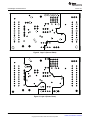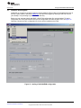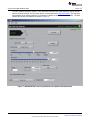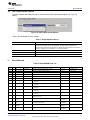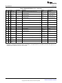
1
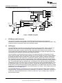
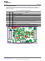
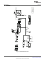
User's Guide
SLAU211A – March 2007 – Revised November 2009
DAC8560 Evaluation Module
This user’s guide describes the characteristics, operation, and the use of the DAC8560 evaluation module
(EVM). It covers all pertinent areas to properly use this EVM board along with the devices that it supports.
The physical PCB layout, schematic diagram, and circuit descriptions are included.
1
2
3
4
5
6
Contents
EVM Overview ............................................................................................................... 2
PCB Design and Performance ............................................................................................ 4
EVM Operation .............................................................................................................. 8
Related Documentation from Texas Instruments ..................................................................... 15
Using the DAC8560 EVM with DXP .................................................................................... 15
Bill of Materials ............................................................................................................. 19
List of Figures
1
EVM Block Diagram ........................................................................................................ 4
2
Top Silkscreen............................................................................................................... 5
3
Layer 1 (Top Signal Plane) ................................................................................................ 6
4
Layer 2 (Ground Plane) .................................................................................................... 6
5
Layer 3 (Power Plane)
6
Layer 4 (Bottom Signal Plane) ............................................................................................ 7
7
Bottom Silkscreen ........................................................................................................... 7
8
INL and DNL Characteristic Plot .......................................................................................... 8
9
DAC8560EVM Default Jumper Configuration ........................................................................... 9
10
DAC8560EVM Schematic ................................................................................................ 14
11
MMB0 with DAC8560EVM Installed
12
13
14
.....................................................................................................
....................................................................................
Loading a DAC8560EVM Configuration ................................................................................
DAC8560EVM: Frequency/Amplitude and Update Rate Adjustments .............................................
DAC Output Update Options .............................................................................................
7
16
17
18
19
List of Tables
1
Factory Default Jumper Settings .......................................................................................... 9
2
DAC Output Channel Mapping
3
4
5
6
7
8
..........................................................................................
Unity Gain Output Jumper Settings .....................................................................................
Gain of Two Output Jumper Settings ...................................................................................
Capacitive Load Drive Output Jumper Settings .......................................................................
Jumper Setting Functions ................................................................................................
Output Update Features ..................................................................................................
DAC8560EVM Parts List .................................................................................................
10
11
11
12
12
19
19
Microsoft, Windows are registered trademarks of Microsoft Corporation.
LabVIEW is a registered trademark of National Instruments.
All other trademarks are the property of their respective owners.
SLAU211A – March 2007 – Revised November 2009
Submit Documentation Feedback
Copyright © 2007–2009, Texas Instruments Incorporated
DAC8560 Evaluation Module
1
EVM Overview
1
www.ti.com
EVM Overview
This section gives a general overview of the DAC8560 evaluation module (EVM), and describes some of
the factors to consider when using this module.
1.1
Features
This EVM features the DAC8560 digital-to-analog converter (DAC). The DAC8560EVM is a simple
evaluation module designed to quickly and easily evaluate the functionality and performance of the 16-bit
high-resolution, single-channel, and serial input DAC with a built-in 2.5-V internal reference that is enabled
by default. This EVM features a serial interface to communicate with any host microprocessor or TI DSP
base system.
Although the DAC was designed for single-supply operation, a bipolar output range is also possible by
configuring the output operational amplifier circuit properly. This is discussed in detail in section 3.2.3. In
addition, the external operational amplifier is also installed as an option to provide output signal
conditioning or boost capacitive load drive and for other output mode requirements desired.
A +5-V precision voltage reference is provided via U3 as well as a 4.096-V precision reference via U4.
These references are optional voltage reference provided externally in case the user needs to evaluate
the DAC8560 with external reference circuits. The external +5-V and +4-V reference source can be
selected via W8 and W4 jumper configuration.
There is also a provision for possibly experimenting with different circuit loads on the reference of the
DAC8560. These are available through R16, C6, and a small 4x4 through-hole grid.
1.2
Power Requirements
The following sections describe the power requirements of this EVM.
1.2.1
Supply Voltage
The dc power supply requirement for this DAC8560EVM (VDD) is selectable between +3.3 V and +5 V via
the W1 jumper header. The +3.3 V comes from J6-8 and the +5 V comes from J6-3 terminal. These
power-supply voltages are referenced to ground through the J6-6 terminal. The VSS and VCC are only
used by the U2 operational amplifier and the U3 voltage reference, which ranges from -15 V to +15 V
maximum and connects through J6-1 and J6-2 terminals, respectively. All the analog power supplies are
referenced to analog ground through J6-6 terminal.
CAUTION
To avoid potential damage to the EVM board, ensure that the correct cables
are connected to their respective terminals as labeled on the EVM board.
Stresses greater than the maximum listed voltage ratings may cause
permanent damage to the device.
The negative rail of the output operational amplifier, U2, can be selected between VSS and AGND via the
W5 jumper. The external operational amplifier is installed as an option to provide output signal
conditioning or for other desired output mode requirements.
CAUTION
To avoid potential damage to the EVM board, ensure that the correct cables
are connected to their respective terminals as labeled on the EVM board.
Stresses greater than the maximum listed voltage ratings may cause
permanent damage to the device.
2
DAC8560 Evaluation Module
SLAU211A – March 2007 – Revised November 2009
Submit Documentation Feedback
Copyright © 2007–2009, Texas Instruments Incorporated
EVM Overview
www.ti.com
1.2.2
Reference Voltage
The DAC8560 comes with a +2.5-V internal reference that is enabled by default. The +2.5-V internal
reference can be measured from its VREF pin, which can be used to source other devices that requires
+2.5-V reference. Because the DAC8560’s internal reference is enabled by default, care should be taken
to ensure that the W4 and W8 jumper headers are open. Otherwise, inaccurate performance or damage to
the part can result. However, the DAC8560 should not be damaged, providing that the external voltage
that is applied to the VREF pin does not exceed the applied voltage in the VDD pin, and it does not exceed
100 mA of sourcing current. It is not recommended to leave the external voltage applied on the VREF pin if
the internal reference is not disabled. The external reference source should be disconnected immediately,
and the EVM power must be recycled to ensure correct performance of the device.
The +5-V and +4-V precision voltage references are provided as an optional reference source to supply
the external voltage reference for the DAC through REF02 (U3) and REF3240 (U4). These reference
voltages are selectable via the jumper W8. When shorting pins 1 and 2, the +5-V reference is selected
whereas shorting pins 2 and 3 selects +4-V reference. The jumper W4 must be shorted between pins 1
and 2 in order for these reference sources to propagate through the DAC.
The +5-V reference voltage goes through an adjustable 100-kΩ potentiometer, R11, in series with 20-kΩ
R10, to allow the user to adjust the reference voltage to its desired settings. The voltage reference then is
buffered through U5 as seen by the device under test. The REF02 precision reference is powered by VCC
(+15 V) through J6-1 terminal.
The REF3240 precision reference is powered by +5 VA through J6-3 terminal.
The test point TP1 also is provided, as well as J4-20, to allow the user to connect other external reference
source if the onboard reference circuit is not desired. The external voltage reference should not exceed
the applied power supply, VDD, of the DAC under test.
CAUTION
When applying an external voltage reference through TP1 or J4-20, ensure that
it does not exceed the applied VDD. Otherwise, this can permanently damage
the DAC8560, U1, device under test.
1.3
EVM Basic Functions
This EVM is designed primarily as a functional evaluation platform to test certain functional characteristics
of the DAC8560 digital-to-analog converter (DAC). Functional evaluation of the installed DAC device can
be accomplished with the use of any microprocessor, TI DSP, or some sort of a signal/waveform
generator.
The headers J2 (top side) and P2 (bottom side) are pass-through connectors provided to allow the control
signals and data required to interface a host processor or waveform generator to the DAC8560EVM using
a custom-built cable.
The DAC output can be monitored through the selected pins of J4 header connector. The output can be
switched through its respective jumper W2 whereas the sense pin VFB also can be switched through its
respective jumper W7 for the reason of stacking. The VFB pin is discussed further in section 3 of this user’s
guide manual. Stacking allows a total of two (DAC8560) DAC channels to be used provided the frame
synchronization signal, SYNC, is unique for each EVM board stacked.
In addition, the option of selecting the DAC output to be fed to the noninverting side of the output
operational amplifier, U2, is also possible by using a jumper across the selected pins of J4. The output
operational amplifier, U2, must be first configured correctly for the desired waveform characteristic (see
Section 3 of this document).
SLAU211A – March 2007 – Revised November 2009
Submit Documentation Feedback
Copyright © 2007–2009, Texas Instruments Incorporated
DAC8560 Evaluation Module
3
PCB Design and Performance
www.ti.com
A block diagram of the EVM is shown in Figure 1.
VCC
VCC
VSS
+ 3 .3 VA
W1
External +4 V
Reference
Module +5V
+ 5VA
W8
GND
VSS
GND
VDD
+5 VA
+3 .3 VA
(J1 )
(J5 )
(J6 )
(P 6)
W4
TP 1
V REF H
VREF H
VDD
SCLK
VOUT
DAC Module DIN
VFB
SYNC
GND
W2
DAC Out
TP 3
Output
Buffer
Module
(J 4)
(P 4)
W7
W3
(J 2)
(P 2)
SCLK
DIN
CS
FSX
TP 2
W6
W15
W5
VSS
Figure 1. EVM Block Diagram
2
PCB Design and Performance
This section discusses the layout design of the PCB, describes the physical and mechanical
characteristics of the EVM, and provides a brief description of the EVM test performance procedure. Also
included is the list of components used on this evaluation module.
2.1
PCB Layout
The DAC8560EVM is designed to preserve the performance quality of the DAC, device under test, as
specified in the data sheet. To take full advantage of the EVM's capabilities, use care during the
schematic design phase to properly select the right components and to build the circuit correctly. The
circuit should include adequate bypassing, identifying and managing the analog and digital signals, and
understanding the components' electrical and mechanical attributes.
The main design concern during the layout process is the optimal placement of components and the
proper routing of signals. Place the bypass capacitors as close as possible to the pins; properly separate
the analog and digital signals from each other. In the layout process, carefully consider the power and
ground plane because of their importance. A solid plane is ideally preferred, but because of its greater
cost, sometimes a split plane can be used satisfactorily. When considering a split plane design, analyze
the component placement and carefully split the board into its analog and digital sections starting from the
DUT. The ground plane plays an important role in controlling the noise and other effects that otherwise
contributes to the error of the DAC output. To ensure that the return currents are handled properly, route
the appropriate signals only in their respective sections, meaning that the analog traces should only lay
directly above or below the analog section and the digital traces in the digital section. Minimize the length
of the traces but use the biggest possible trace width allowable in the design. These design practices are
illustrated in Figure 2 through Figure 7.
The DAC8560EVM board is constructed on a four-layer printed-circuit board using a copper-clad FR-4
laminate material. The printed-circuit board has a dimension of 43,1800 mm (1.7000 inch) × 82,5500 mm
(3.2500 inch), and the board thickness is 1,5748 mm (0.062 inch). Figure 2 through Figure 6 show the
individual artwork layers.
4
DAC8560 Evaluation Module
SLAU211A – March 2007 – Revised November 2009
Submit Documentation Feedback
Copyright © 2007–2009, Texas Instruments Incorporated
PCB Design and Performance
www.ti.com
Figure 2. Top Silkscreen
Figure 3. Layer 1 (Top Signal Plane)
SLAU211A – March 2007 – Revised November 2009
Submit Documentation Feedback
Copyright © 2007–2009, Texas Instruments Incorporated
DAC8560 Evaluation Module
5
PCB Design and Performance
www.ti.com
Figure 4. Layer 2 (Ground Plane)
Figure 5. Layer 3 (Power Plane)
6
DAC8560 Evaluation Module
SLAU211A – March 2007 – Revised November 2009
Submit Documentation Feedback
Copyright © 2007–2009, Texas Instruments Incorporated
PCB Design and Performance
www.ti.com
Figure 6. Layer 4 (Bottom Signal Plane)
Figure 7. Bottom Silkscreen
SLAU211A – March 2007 – Revised November 2009
Submit Documentation Feedback
Copyright © 2007–2009, Texas Instruments Incorporated
DAC8560 Evaluation Module
7
EVM Operation
2.2
www.ti.com
EVM Performance
The EVM performance test is performed using a high-density DAC bench test board, an Agilent 3458A
digital multimeter, and a PC running the LabVIEW® software. The EVM board is tested for all codes of
65535 and the device under test (DUT) is allowed to settle for 1 ms before the meter is read. This process
is repeated for all codes to generate the measurements for INL and DNL.
Figure 8 shows the characteristic INL and DNL plots.
Figure 8. INL and DNL Characteristic Plot
3
EVM Operation
This section covers in detail the operation of the EVM to provide guidance to the user in evaluating the
onboard DAC and how to interface the EVM to a specific host processor.
See the DAC8560 data sheet, SLAS264, for information about its serial interface and other related topics.
The EVM board is factory tested and configured to operate in the unipolar output mode.
8
DAC8560 Evaluation Module
SLAU211A – March 2007 – Revised November 2009
Submit Documentation Feedback
Copyright © 2007–2009, Texas Instruments Incorporated
EVM Operation
www.ti.com
3.1
Factory Default Settings
The EVM board is set to its default configuration from factory as described in Table 1 to operate in
unipolar +2.5-V mode of operation. Figure 9 shows the default jumper configuration as described in the
table for the DAC8560.
Table 1. Factory Default Jumper Settings
Reference
Jumper
Position
W1
1-2
Analog supply for the DAC8560 is +5 VA.
W2
1-2
DAC output (VOUT) is routed to J4-2.
W3
OPEN
VREF is not routed to the inverting input of the operational amplifier for voltage offset (for bipolar mode of
operation).
W4
OPEN
Onboard external buffered reference U3 or U4 is not routed to VREF.
W5
1-2
Negative supply rail of U2 operational amplifier is supplied with VSS.
W6
1-2
CS signal from J2 is used for frame synchronization, SYNC, signal.
W7
OPEN
For DAC8560EVM, the VFB is not routed out unless there is a need to minimize the output error. If using
W7, remove R1 and short W7, then connect VFB and VOUT as close as possible to the load.
W8
OPEN
Onboard external buffered reference U3 or U4 are not selected. Default is the +2.5-V internal reference of
the DAC8560.
W15
OPEN
Output operational amplifier, U2, is configured as voltage follower.
J4
1-2
Function
DAC output (VOUT) is connected to the noninverting input of the output operational amplifier, U2.
Figure 9. DAC8560EVM Default Jumper Configuration
SLAU211A – March 2007 – Revised November 2009
Submit Documentation Feedback
Copyright © 2007–2009, Texas Instruments Incorporated
DAC8560 Evaluation Module
9
EVM Operation
3.2
www.ti.com
Host Processor Interface
The host processor basically drives the DAC; so, the DAC's proper operation depends on the successful
configuration between the host processor and the EVM board. In addition, a properly written code also is
required to operate the DAC.
A custom cable can be made specific to the host interface platform. The EVM allows interface to the host
processor through J2 header connector for the serial control signals and the serial data input. The output
can be monitored through the J4 header connector.
An interface adapter board also is available for a specific TI DSP starter kit as well as an MSP430-based
microprocessor as previously mentioned. Using the interface board alleviates the tedious task of building
customized cables and allows easy configuration of a simple evaluation system.
The DAC8560 interfaces with any host processor capable of handling SPI protocols or the popular TI
DSP. For more information regarding the DAC8560 data interface, see the DAC8560 data sheet
(SLAS464).
3.3
EVM Stacking
The stacking of EVMs is possible if the user needs to evaluate two DAC8560 devices to yield a total of up
to two (DAC8560) channel outputs. A maximum of two EVMs are allowed because the output terminal, J4,
dictates the number of DAC channels that can be connected without output bus contention. Table 2 shows
how the DAC output channels are mapped into the output terminal, J4, with respect to the jumper position
of W2 and W7.
Table 2. DAC Output Channel Mapping
Reference
W2
W7
Jumper
Position
Function
1-2
DAC output (VOUT) is routed to J4-2.
2-3
DAC output (VOUT) is routed to J4-6.
1-2
DAC sense pin (VFB) is routed to J4-10, if R1 jumper resistor is disconnected.
2-3
DAC sense pin (VFB) is routed to J4-14, if R1 jumper resistor is disconnected.
In order to allow exclusive control of each EVM that is stacked together, the DAC8560 must have a
separate SYNC signal. This is accomplished in hardware by routing the SYNC signal of the first EVM
through CS (P2/J2 pin 1) by shorting pins 1-2 of jumper W6. The second EVM should use the FSX signal
(P2/J2 pin 7) to drive the SYNC signal by shorting pins 2-3 of the jumper W6. The output can be mapped
as described in Table 2 for each of the EVM stacked.
3.4
The Output Operational Amplifier
The EVM includes an optional signal-conditioning circuit for the DAC output through an external
operational amplifier, U2. During stacking of the EVMs, only one DAC output channel can be monitored at
any given time for evaluation because the odd-numbered pins (J4-1 to J4-7) are tied together. If both
outputs are needed to be buffered and monitored at the same time, the traces in the back of the EVM
board are exposed for ease of cutting. When cutting a trace, make sure to cut through the trace adjacent
to the appropriate J4 header pin and not at the curvy line. If the trace is cut through the curving line, the
signal may not propagate through to the operational amplifier. See Figure 6 and the schematic included in
this manual.
The output operational amplifier is set to unity gain configuration by default but can be modified by simple
jumper settings. Nevertheless, the raw output of the DAC can be probed through the specified pins of the
J4 output terminal, which also provides mechanical stability when stacking or plugging into any interface
board. In addition, it provides easy access for monitoring up to two (DAC8560) DAC channels when
stacking two EVMs together (see section 3.3).
The following sections describe the different configurations of the output amplifier, U2.
10
DAC8560 Evaluation Module
SLAU211A – March 2007 – Revised November 2009
Submit Documentation Feedback
Copyright © 2007–2009, Texas Instruments Incorporated
EVM Operation
www.ti.com
3.4.1
Unity Gain Output
The buffered output configuration can be used to prevent loading the DAC8560, although it may present
some slight distortion because of the feedback resistor and capacitor. The user can tailor the feedback
circuit to closely match the desired wave shape by simply desoldering R6 and C12 and replacing them
with components of the desired values. Additionally, C12 can be eliminated and R6 can be replaced with a
0Ω resistor to simplify the feedback circuit.
Table 3 shows the jumper setting for the unity gain configuration of the DAC external output buffer in
unipolar or bipolar mode.
Table 3. Unity Gain Output Jumper Settings
Reference
3.4.2
Jumper Setting
Unipolar
Bipolar
W3
Open
Open
W5
2-3
1-2
W15
Open
Open
Function
Disconnect VREF from the inverting input of the operational amplifier.
Supplies VSS to the negative rail of operational amplifier or ties it to AGND.
Disconnect the negative input of the operational amplifier from the gain resistor, R12.
Output Gain of Two or Bipolar Operation
Two types of configurations yield a gain of two output, depending on the setup of the jumpers W3 and
W15. These configurations allow the user to choose a DAC output having VREF as an offset or not.
Table 4 shows the proper jumper settings of the EVM for the 2× gain output of the DAC.
Table 4. Gain of Two Output Jumper Settings
Reference
Jumper Setting
Bipolar
Close
Close
Inverting input of the output operational amplifier, U2, is connected to VREF for use as its offset
voltage for bipolar operation. W15 jumper must be open.
Open
Open
VREF is disconnected from the inverting input of the output operational amplifier, U2. W15
jumper must be close to achieve gain of 2 output.
2-3
1-2
Supplies power, VSS, to the negative rail of operational amplifier, U2, for bipolar mode, or ties it
to AGND for unipolar mode.
Close
Close
Configures operational amplifier, U2, for a gain of 2 output without a voltage offset. W3 jumper
must be open.
Open
Open
Inverting input of the operational amplifier, U2, is disconnected from the gain resistor, R12. W3
jumper must be close.
W3
W5
W15
3.4.3
Function
Unipolar
Capacitive Load Drive
Another output configuration option is to drive a wide range of capacitive load requirement. However, all
operational amplifiers under certain conditions may become unstable depending on the operational
amplifier configuration, gain, and load value. These are just few factors that can affect operational
amplifiers stability performance and should be considered when implementing.
In unity gain, the OPA627 operational amplifier, U2, performs well with large capacitive loads. Increasing
the gain enhances the amplifier’s ability to drive even more capacitance, and by adding a load resistor
even improves the capacitive load drive capability.
SLAU211A – March 2007 – Revised November 2009
Submit Documentation Feedback
Copyright © 2007–2009, Texas Instruments Incorporated
DAC8560 Evaluation Module
11
EVM Operation
www.ti.com
Table 5 shows the jumper setting configuration for a capacitive load drive.
Table 5. Capacitive Load Drive Output Jumper Settings
Reference
3.5
Jumper Setting
Unipolar
Bipolar
W3
Open
Open
W5
2-3
1-2
W15
Open
Open
Function
VREF is disconnected from the inverting input of the output operational amplifier, U2.
Supplies power, VSS, to the negative rail of operational amplifier, U2, for bipolar mode, or ties it
to AGND for unipolar mode.
Capacitive load drive output of DAC is routed to pin 1 of W15 jumper and can be used as the
output terminal.
Jumper Settings
Table 6 shows the function of each specific jumper setting of the EVM.
Table 6. Jumper Setting Functions
Reference
Jumper
Position
1
Function
3
+5-V analog supply is selected for AVDD.
W1
1
3
+3.3-V analog supply is selected for AVDD.
1
3
Routes VOUT to J4-2.
W2
1
3
Routes VOUT to J4-6.
Disconnects VREF to the inverting input of the output operational amplifier, U2
W3
Connects VREF to the inverting input of the output operational amplifier, U2
1
3
Routes the adjustable, onboard +5-V reference or the fixed +4-V reference to the VREF input of the
DAC8560.
1
3
This is the default jumper position for DAC8560EVM because the +2.5-V internal reference is enabled
by default.
1
3
W4
Routes the user-supplied reference from TP1 or J4-20 to the VREF input of the DAC8560.
1
3
Negative supply rail of the output operational amplifier, U2, is powered by VSS for bipolar operation.
W5
1
3
Negative supply rail of the output operational amplifier, U2, is tied to AGND for unipolar operation.
1
3
CS signal from J2-1 is routed to drive the SYNC signal of the DAC8560.
W6
1
3
FSX signal from J2-7 is routed to drive the SYNC signal of the DAC8560.
12
DAC8560 Evaluation Module
SLAU211A – March 2007 – Revised November 2009
Submit Documentation Feedback
Copyright © 2007–2009, Texas Instruments Incorporated
EVM Operation
www.ti.com
Table 6. Jumper Setting Functions (continued)
Reference
Jumper
Position
1
3
1
3
W7
Function
For DAC8560EVM, the VFB is routed out to minimize the output error. Remove R1 and short W7 as
shown; then connect VFB and VOUT as close as possible to the load. The VFB signal will be routed to
J4-10.
This is the default jumper position for DAC8560EVM when R1 is installed.
1
3
1
3
For DAC8560EVM, the VFB is routed out to minimize the output error. Remove R1 and short W7 as
shown then connect VFB and VOUT as close as possible to the load. The VFB signal will be routed to
J4-14.
This jumper position selects the adjustable +5-V reference to route to the VREF input of the DAC8560.
1
3
1
3
W8
This is the default jumper position for DAC8560EVM because the +2.5-V internal reference is enabled
by default.
This jumper position selects the +4-V reference to route to the VREF input of the DAC8560.
Disconnects the inverting input of the output operational amplifier, U2, from the gain resistor, R12.
W15
Legend:
Connects the inverting input of the output operational amplifier, U2, to the gain resistor, R12, for gain
of 2 configuration.
Indicates the corresponding pins that are shorted or closed.
SLAU211A – March 2007 – Revised November 2009
Submit Documentation Feedback
Copyright © 2007–2009, Texas Instruments Incorporated
DAC8560 Evaluation Module
13
Copyright © 2007–2009, Texas Instruments Incorporated
R5 DNP
R25 DNP
R7 DNP
GPIO5
CS
SCLK
CLKR
FSX
FSR
SDI
DR
2
4
6
8
10
12
14
16
18
20
GPIO0
C3
0.1µF
C11
10µF
C2
0.47µF
SDA
GPIO3
GPIO4
SCL
GPIO1
GPIO2
VCC
Serial Header
1
3
5
7
9
11
13
15
17
19
5
2
8
7
REF3240
ENABLE
R9
20K
4
5
6
FSX
CS
REF02AU(8)
6
3
1
2
IN
GND_S OUT_S
GND_F OUT_F
U4
TRIM OUT
V+ TEMP
NC
NC
NC
U3
3
2
1
GND
4
1
3
J2
3
1
Do not populate
R5, R7, & R25
2
100K
R10
20K
3
SDI
SCLK
R11
2
TP4
W6
0
0
0
VCC
R4
R3
R2
7
4
8
6
OPA227
U5
7
6
5
C7
0.1µF
W8
DAC8560
DIN
SCLK
SYNC
U1
GND
VREF
VOUT
VFB
VDD
1
3
1
8
2
4
3
+REFin
W4
VFB
TP5
TP2
TP1
W1
C5
10µF
EXTERNAL
REFERENCE
C4
100pF
0
C1
0.1µF
R1
+5VA
OUT_A
C6
R16
DNP
DNP
Typical 1µF
Typical 10K
+3.3VA
W7
W2
VFB_B
VFB_A
OUT_A2
OUT_A1
+3.3VD+1.8VD +5VA
-REFin
+REFin
VCC
1
3
5
7
9
11
13
15
17
19
1
3
5
7
9
J6
2
4
6
8
10
OUTPUT HEADER
2
4
6
8
10
12
14
16
18
20
J4
VSS
W3
0
R12
10K
W15
U2_-IN
R8
-5VA +3.3VA VDD
R14
10K
U2_+IN
2
3
U2
C9
6
U2_OUT
VSS
OPA627AU
1µF
100
R13
DAC8560EVM BOM = 6484154
DAC8560EVM PWB = 6484155
DAC8560EVM DDB = 6484156 (BLOCK)
DAC8560EVM PCA = 6484157
DAC8560EVM KIT = 6484158 (BLOCK)
EDGE Numbers:
1nF
10K
R6
1µF
W5
C12
4
C10
VCC
7
DAC8560 Evaluation Module
5
14
1
TP3
VOUT
3.6
AVDD
EVM Operation
www.ti.com
Schematic
Figure 10. DAC8560EVM Schematic
SLAU211A – March 2007 – Revised November 2009
Submit Documentation Feedback
Related Documentation from Texas Instruments
www.ti.com
4
Related Documentation from Texas Instruments
To obtain a copy of any of the following TI documents, call the Texas Instruments Literature Response
Center at (800) 477-8924 or the Product Information Center (PIC) at (972) 644-5580. When ordering,
identify this manual by its title and literature number. Updated documents also can be obtained through
the TI Web site at www.ti.com.
Related Documentation
5
Data Sheet
Literature Number
DAC8560
SBAS254
REF02
SBVS003
REF3240
SBVS058
OPA627
SBOS165
OPA227
SBOS110
Using the DAC8560 EVM with DXP
The DAC8560EVM is compatible with the DAC eXerciser Program (DXP) from Texas Instruments. DXP is
a tool that can generate the necessary control signals required to output various signals and waveforms
from the device installed on the DAC8560EVM. The DAC8560EVM-PDK kit combines the DAC8560EVM
board with the DSP-based MMB0 modular motherboard. The kit includes the DXP software for evaluation
using any available USB port on a Microsoft® Windows® XP-based computer.
DXP is a program that controls the digital input signals such as the clock, CS, and SDI. Wave tables are
built into the DSP software to allow sine, ramp, triangle, and square wave signals to be generated by the
DAC8560. Straight dc outputs can also be obtained.
The DAC8560EVM-PDK uses the DSP-based MMB0 to control the DAC8560EVM using the DXP
software. For complete information about installing and configuring DXP, see the DXP User's Guide,
available for download from the TI web site. This section covers the specific operation of the
DAC8560EVM-PDK.
5.1
Hardware
The hardware consists of two primary components: the DAC8560EVM itself and a modular motherboard
called the MMB0. The MMB0 board houses a TMS320VC5507 DSP that controls the serial interface to the
device loaded on the EVM board.
The hardware must be configured such that the DAC8560EVM is plugged onto the MMB0, aligning female
connectors J4, J2, and J6 (on the bottom side of the DAC8560EVM) with male connectors J7, J4, and J5
on the MMB0. The assembled hardware is shown in Figure 11.
CAUTION
Be sure to exercise caution when assembling the boards. It is possible to
misalign the connectors and damage both the EVM and the motherboard.
CAUTION
DO NOT connect the MMB0 to your PC before installing the DXP software as
described in the DXP User’s Guide. Installing the software first ensures that the
necessary drivers are properly loaded to run the hardware.
SLAU211A – March 2007 – Revised November 2009
Submit Documentation Feedback
Copyright © 2007–2009, Texas Instruments Incorporated
DAC8560 Evaluation Module
15
Using the DAC8560 EVM with DXP
www.ti.com
Figure 11. MMB0 with DAC8560EVM Installed
5.2
MMB0 Power Supplies
Several power connections are required for the hardware to work properly. For the MMB0, the supplied
6-V ac/dc converter is all that is necessary. Be sure that J12 on the MMB0 board is closed before
connecting the ac/dc adapter to the DC In connector of the MMB0. This supply provides all power to the
digital portion of the DAC8560EVM as well as all necessary power for the DSP. Clean, well-regulated
analog power for the DAC8560EVM should be supplied externally via J14, a six-position screw terminal
mounted in the lower left corner of the MMB0 board.
CAUTION
When using external power supplies applied to J14 on the MMB0, please
ensure all shorting blocks from J13 are completely removed. Permanent
damage to the MMB0 may occur otherwise
From left to right, the J14 screw terminal connections are –VA, +VA, +5VA, –5VA, +5VD, and GND. The
5V from the ac/dc adapter can be connected to the +VA or the +5VA by installing a jumper across JP13A
or JP13B. If the jumpers are not installed, the analog VSS, VCC, +5VA, and –5VA may be applied directly to
the –VA, +VA, +5VA, and –5VA screw terminals at J14 on the MMB0 (referenced to the GND terminal).
The DAC8581 board power requirements are described in Section 1.2.1 of this manual.
16
DAC8560 Evaluation Module
SLAU211A – March 2007 – Revised November 2009
Submit Documentation Feedback
Copyright © 2007–2009, Texas Instruments Incorporated
Using the DAC8560 EVM with DXP
www.ti.com
5.3
Software: Running DXP
Install DXP on a laptop or personal computer running Windows XP according to the detailed instruction in
the DXP Users Guide (TI document SBAU146). Run the DXP program by clicking on the DXP icon on
your desktop, or by browsing to your installation directory.
Before you can generate signals with DXP, a DAC EVM configuration file must be loaded. To load a
configuration file, select the desired DAC from the configuration list under the DAC menu, as Figure 12
illustrates. Choose the DAC configuration file for the device installed on the EVM.
Figure 12. Loading a DAC8560EVM Configuration
SLAU211A – March 2007 – Revised November 2009
Submit Documentation Feedback
Copyright © 2007–2009, Texas Instruments Incorporated
DAC8560 Evaluation Module
17
Using the DAC8560 EVM with DXP
www.ti.com
The DXP software defaults to output a 1-kHz sine wave from the DAC. Other waveform options include
square, sawtooth, triangle, and dc output options, as described in the DXP User's Guide. The frequency
and amplitude of the output waveform are controlled by sliders on the DXP software interface. The DAC
update rate can also be modified, as shown in Figure 13.
Figure 13. DAC8560EVM: Frequency/Amplitude and Update Rate Adjustments
18
DAC8560 Evaluation Module
SLAU211A – March 2007 – Revised November 2009
Submit Documentation Feedback
Copyright © 2007–2009, Texas Instruments Incorporated
Bill of Materials
www.ti.com
5.4
DAC Output Update Options
The DXP software also allows the user to choose several DAC output update options, as Figure 14
shows.
Figure 14. DAC Output Update Options
Table 7 lists the details on these options.
Table 7. Output Update Features
Options
Detailed Description
Frame Sync
The DXP software defaults to Frame Sync. The Frame Sync output of the MMB0
connects to the SYNC input of the DAC8560. The DAC output changes to the
corresponding level when the DAC latch is updated via SDI. Ensure the shunt jumper
on W6 is covering pins 2-3 (default is 1-2) to use this feature.
Latch with DSP Timer
N/A
Latch with External Timer
N/A
Update Rate
6
User Input - enter the desired DAC update rate, 1MSPS is the default
Bill of Materials
Table 8. DAC8560EVM Parts List
Item
Qty
Value
Designators
Description
Vendor
Vendor Part No.
1
3
10kΩ
R6 R12 R14
1/8W 1206 Thick Film Chip Resistor, ±1% Tol
Panasonic
ERJ-8ENF1002V
2
1
20kΩ Trim Pot
R9
5T Potentiometer, 4mm SMD, Cermet
Bourns
3214W-1-203E
3
5
0Ω
R1–R4 R8
1/4 W 1206 Thick Film Chip Resistor, ±5% Tol
Panasonic
ERJ-8GEY0R00V
4
1
100 Ω
R13
1/4W 1206 Thick Film Chip Resistor, ±5% Tol
Panasonic
ERJ-8GEYJ101V
5
1
20kΩ
R10
1/4W 1206 Thick Film Chip Resistor, ±5% Tol
Panasonic
ERJ-8GEYJ203V
6
1
100kΩ Trim Pot R11
Potentiometer, 4mm SMD, Cermet
Bourns
3214W-1-104E
7
3
0.1μF
C1 C3 C7
Multilayer Ceramic Chip Capacitor, 1206 SMD, 25V, ±15%
TC, ±10% Tol
TDK
C3216X7R1E104KT
8
2
1μF
C9 C10
Multilayer Ceramic Chip Capacitor, 1210 SMD, 25V, ±15%
TC, ±10% Tol
TDK
C3225X7R1E105KT
9
1
1nF
C12
Multilayer Ceramic Chip Capacitor, 1206 SMD, 25V, ±15%
TC, ±10% Tol
TDK
C3216X7R1H102KT
10
1
0.47μF
C2
Multilayer Ceramic Chip Capacitor, 1206 SMD, 50V, ±15%
TC, ±10% Tol
TDK
C3216X7R1H474KT
11
2
10μF
C5 C11
Multilayer Ceramic Chip Capacitor, 1210 SMD, 25V, ±15%
TC, ±10% Tol
TDK
C3225X7R1E106KT
12
1
100pF
C4
Multilayer Ceramic Chip Capacitor, 0603 SMD, 50V,
30ppm/°C, ±5% Tol
TDK
C1608COG1H101J
13
1
Bipolar
Op-Amp
U5
8-SOP(D) High Precision Low Noise Op-Amp
Texas
Instruments
OPA227UA
14
1
16-Bit String
DAC
U1
MSOP-8(DGK), 1-CH, SPI, Low Glitch, Voltage Output
DAC with Internal reference
Texas
Instruments
DAC8560IDDGK
15
1
4.096V
Reference
U4
4ppm/°C, 100µA, SOT23-6 VOLTAGE REFERENCE
Texas
Instruments
REF3240AIDBV
16
1
5V Reference
U3
15ppm/°C, ±0.2% Tol Output, SOIC-8, Voltage Reference
Texas
Instruments
REF02AU
SLAU211A – March 2007 – Revised November 2009
Submit Documentation Feedback
Copyright © 2007–2009, Texas Instruments Incorporated
DAC8560 Evaluation Module
19
Bill of Materials
www.ti.com
Table 8. DAC8560EVM Parts List (continued)
Item
Qty
Value
Designators
Description
Vendor
Vendor Part No.
17
1
Difet Op-Amp
U2
8-SOP(D) Precision High-Speed, Difet Op-Amp
Texas
Instruments
OPA627AU
18
2
10 × 2 × 0.1
SMT
J2 J4
20-PIN Terminal Strip
Samtec
TSM-110-01-S-DV-M
19
1
5 × 2 × 0.1
SMT
J6
10-PIN Terminal Strip
Samtec
TSM-105-01-T-DV
20
2
10 × 2 × 0.1
SMT
P2 P4
20-PIN Socket Strip
Samtec
SSW-110-22-S-D-VS-P
21
1
5 × 2 × 0.1
SMT
P6 10-PIN Socket Strip (1)
Samtec
SSW-105-22-F-D-VS-K
22
5
1 × 1 × 0.061D
TH
TP1–TP5
Turret Terminal Pin
Mill-Max
2348-2-00-01-00-00-07-0
23
2
3 × 1 × 0.7874
TH
W2 W7
3-PIN Terminal Strip
Samtec
TMM-103-01-T-S
24
2
2 × 1 × 0.1 TH
W3 W15
Modified 0.025" Square Post Header
Samtec
MTSW-102-08-T-S-295
25
5
3 x 1 × 0.1 TH
W1 W4–W6 W8
Modified 0.025" Square Post Header
Samtec
MTSW-103-08-T-S-295
26
0
N/A
N/A
Schematic Diagram
Texas
Instruments
6484156
27
1
N/A
N/A
Printed Wiring Board
Texas
Instruments
6484155
28
0
N/A
N/A
Printed Circuit Assembly
Texas
Instruments
6484157
29
0
N/A
N/A
29 0 N/A N/A Kit Assembly
Texas
Instruments
6484158
30
5
Do Not
Populate
C6 R5 R7 R16
R25
Do not install these components (1)
31
1
2mm Shunt
N/A
Shorting Block for W2
Samtec
2SN-BK-G
32
6
0.100 Shorting
Blocks
N/A
Shorting Blocks
Samtec
SNT-100-BK-G-H
(1)
20
(1)
P2, P4, and P6 parts are not shown in the schematic diagram. All the P-designated parts are installed in the bottom side of the PC board
opposite the J-designated counterpart. Example, J2 is installed on the topside whereas P2 is installed in the bottom side opposite of J2.
Do NOT install the following: C6, R5, R7, R16, and R25.
DAC8560 Evaluation Module
SLAU211A – March 2007 – Revised November 2009
Submit Documentation Feedback
Copyright © 2007–2009, Texas Instruments Incorporated
Evaluation Board/Kit Important Notice
Texas Instruments (TI) provides the enclosed product(s) under the following conditions:
This evaluation board/kit is intended for use for ENGINEERING DEVELOPMENT, DEMONSTRATION, OR EVALUATION
PURPOSES ONLY and is not considered by TI to be a finished end-product fit for general consumer use. Persons handling the
product(s) must have electronics training and observe good engineering practice standards. As such, the goods being provided are
not intended to be complete in terms of required design-, marketing-, and/or manufacturing-related protective considerations,
including product safety and environmental measures typically found in end products that incorporate such semiconductor
components or circuit boards. This evaluation board/kit does not fall within the scope of the European Union directives regarding
electromagnetic compatibility, restricted substances (RoHS), recycling (WEEE), FCC, CE or UL, and therefore may not meet the
technical requirements of these directives or other related directives.
Should this evaluation board/kit not meet the specifications indicated in the User’s Guide, the board/kit may be returned within 30
days from the date of delivery for a full refund. THE FOREGOING WARRANTY IS THE EXCLUSIVE WARRANTY MADE BY
SELLER TO BUYER AND IS IN LIEU OF ALL OTHER WARRANTIES, EXPRESSED, IMPLIED, OR STATUTORY, INCLUDING
ANY WARRANTY OF MERCHANTABILITY OR FITNESS FOR ANY PARTICULAR PURPOSE.
The user assumes all responsibility and liability for proper and safe handling of the goods. Further, the user indemnifies TI from all
claims arising from the handling or use of the goods. Due to the open construction of the product, it is the user’s responsibility to
take any and all appropriate precautions with regard to electrostatic discharge.
EXCEPT TO THE EXTENT OF THE INDEMNITY SET FORTH ABOVE, NEITHER PARTY SHALL BE LIABLE TO THE OTHER
FOR ANY INDIRECT, SPECIAL, INCIDENTAL, OR CONSEQUENTIAL DAMAGES.
TI currently deals with a variety of customers for products, and therefore our arrangement with the user is not exclusive.
TI assumes no liability for applications assistance, customer product design, software performance, or infringement of
patents or services described herein.
Please read the User’s Guide and, specifically, the Warnings and Restrictions notice in the User’s Guide prior to handling the
product. This notice contains important safety information about temperatures and voltages. For additional information on TI’s
environmental and/or safety programs, please contact the TI application engineer or visit www.ti.com/esh.
No license is granted under any patent right or other intellectual property right of TI covering or relating to any machine, process, or
combination in which such TI products or services might be or are used.
FCC Warning
This evaluation board/kit is intended for use for ENGINEERING DEVELOPMENT, DEMONSTRATION, OR EVALUATION
PURPOSES ONLY and is not considered by TI to be a finished end-product fit for general consumer use. It generates, uses, and
can radiate radio frequency energy and has not been tested for compliance with the limits of computing devices pursuant to part 15
of FCC rules, which are designed to provide reasonable protection against radio frequency interference. Operation of this
equipment in other environments may cause interference with radio communications, in which case the user at his own expense
will be required to take whatever measures may be required to correct this interference.
EVM Warnings and Restrictions
It is important to operate this EVM within the input voltage range of +2.7 V to +5 V and the output voltage range of –5 V to +5 V.
Exceeding the specified input range may cause unexpected operation and/or irreversible damage to the EVM. If there are
questions concerning the input range, please contact a TI field representative prior to connecting the input power.
Applying loads outside of the specified output range may result in unintended operation and/or possible permanent damage to the
EVM. Please consult the EVM User's Guide prior to connecting any load to the EVM output. If there is uncertainty as to the load
specification, please contact a TI field representative.
During normal operation, some circuit components may have case temperatures greater than +30° C. The EVM is designed to
operate properly with certain components above +85° C as long as the input and output ranges are maintained. These components
include but are not limited to linear regulators, switching transistors, pass transistors, and current sense resistors. These types of
devices can be identified using the EVM schematic located in the EVM User's Guide. When placing measurement probes near
these devices during operation, please be aware that these devices may be very warm to the touch.
Mailing Address: Texas Instruments, Post Office Box 655303, Dallas, Texas 75265
Copyright © 2009, Texas Instruments Incorporated
IMPORTANT NOTICE
Texas Instruments Incorporated and its subsidiaries (TI) reserve the right to make corrections, modifications, enhancements, improvements,
and other changes to its products and services at any time and to discontinue any product or service without notice. Customers should
obtain the latest relevant information before placing orders and should verify that such information is current and complete. All products are
sold subject to TI’s terms and conditions of sale supplied at the time of order acknowledgment.
TI warrants performance of its hardware products to the specifications applicable at the time of sale in accordance with TI’s standard
warranty. Testing and other quality control techniques are used to the extent TI deems necessary to support this warranty. Except where
mandated by government requirements, testing of all parameters of each product is not necessarily performed.
TI assumes no liability for applications assistance or customer product design. Customers are responsible for their products and
applications using TI components. To minimize the risks associated with customer products and applications, customers should provide
adequate design and operating safeguards.
TI does not warrant or represent that any license, either express or implied, is granted under any TI patent right, copyright, mask work right,
or other TI intellectual property right relating to any combination, machine, or process in which TI products or services are used. Information
published by TI regarding third-party products or services does not constitute a license from TI to use such products or services or a
warranty or endorsement thereof. Use of such information may require a license from a third party under the patents or other intellectual
property of the third party, or a license from TI under the patents or other intellectual property of TI.
Reproduction of TI information in TI data books or data sheets is permissible only if reproduction is without alteration and is accompanied
by all associated warranties, conditions, limitations, and notices. Reproduction of this information with alteration is an unfair and deceptive
business practice. TI is not responsible or liable for such altered documentation. Information of third parties may be subject to additional
restrictions.
Resale of TI products or services with statements different from or beyond the parameters stated by TI for that product or service voids all
express and any implied warranties for the associated TI product or service and is an unfair and deceptive business practice. TI is not
responsible or liable for any such statements.
TI products are not authorized for use in safety-critical applications (such as life support) where a failure of the TI product would reasonably
be expected to cause severe personal injury or death, unless officers of the parties have executed an agreement specifically governing
such use. Buyers represent that they have all necessary expertise in the safety and regulatory ramifications of their applications, and
acknowledge and agree that they are solely responsible for all legal, regulatory and safety-related requirements concerning their products
and any use of TI products in such safety-critical applications, notwithstanding any applications-related information or support that may be
provided by TI. Further, Buyers must fully indemnify TI and its representatives against any damages arising out of the use of TI products in
such safety-critical applications.
TI products are neither designed nor intended for use in military/aerospace applications or environments unless the TI products are
specifically designated by TI as military-grade or "enhanced plastic." Only products designated by TI as military-grade meet military
specifications. Buyers acknowledge and agree that any such use of TI products which TI has not designated as military-grade is solely at
the Buyer's risk, and that they are solely responsible for compliance with all legal and regulatory requirements in connection with such use.
TI products are neither designed nor intended for use in automotive applications or environments unless the specific TI products are
designated by TI as compliant with ISO/TS 16949 requirements. Buyers acknowledge and agree that, if they use any non-designated
products in automotive applications, TI will not be responsible for any failure to meet such requirements.
Following are URLs where you can obtain information on other Texas Instruments products and application solutions:
Products
Amplifiers
Data Converters
DLP® Products
DSP
Clocks and Timers
Interface
Logic
Power Mgmt
Microcontrollers
RFID
RF/IF and ZigBee® Solutions
amplifier.ti.com
dataconverter.ti.com
www.dlp.com
dsp.ti.com
www.ti.com/clocks
interface.ti.com
logic.ti.com
power.ti.com
microcontroller.ti.com
www.ti-rfid.com
www.ti.com/lprf
Applications
Audio
Automotive
Broadband
Digital Control
Medical
Military
Optical Networking
Security
Telephony
Video & Imaging
Wireless
www.ti.com/audio
www.ti.com/automotive
www.ti.com/broadband
www.ti.com/digitalcontrol
www.ti.com/medical
www.ti.com/military
www.ti.com/opticalnetwork
www.ti.com/security
www.ti.com/telephony
www.ti.com/video
www.ti.com/wireless
Mailing Address: Texas Instruments, Post Office Box 655303, Dallas, Texas 75265
Copyright © 2009, Texas Instruments Incorporated