1
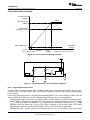
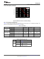
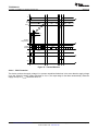
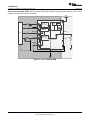
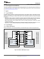
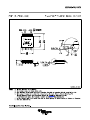
Sample &
Buy
Product
Folder
Support &
Community
Tools &
Software
Technical
Documents
TPS1H100-Q1
SLVSCM2A – OCTOBER 2014 – REVISED JANUARY 2014
TPS1H100-Q1 40-V, 100-mΩ Single-Channel Smart High-Side Power Switch
1 Features
•
•
1
•
•
•
•
•
•
•
•
•
•
•
Qualified for Automotive Applications
AEC-Q100 Qualified With the Following Results:
– Device Temperature Grade 1: –40°C to 125°C
Ambient Operating Temperature Range
– Device HBM ESD Classification Level H3A
– Device CDM ESD Classification Level C4B
Single-Channel Smart High-Side Power Switch
With Full Diagnostics
– Version A: Open-Drain Status Output
– Version B: Current Sense Analog Output
Wide Operating Voltage 3.5 to 40 V
Very-Low Standby Current, <0.5 µA
Operating Junction Temperature, –40 to 150°C
Input Control, 3.3-V and 5-V Logic Compatible
High-Accuracy Current Sense, ±30 mA at 1 A,
±4 mA at 5 mA
Programmable Current Limit With External
Resistor, ±20% at 0.5 A
Diagnostic Enable Function for Multiplexing of
MCU Analog or Digital Interface
Tested According to AECQ100-12 Grade A,
1 Million Times Short to GND Test
Electrical Transient Disturbance Immunity
Certification of ISO7637-2 and ISO16750-2
Protection
– Overload and Short-Circuit Protection
– Inductive Load Negative Voltage Clamp
– Undervoltage Lockout (UVLO) Protection
– Thermal Shutdown/Swing With Self Recovery
•
•
– Loss of GND, Loss of Supply Protection
– Reverse Battery Protection With External
Circuitry
Diagnostic
– On/Off State Output Open/Short to Battery
Detection
– Overload and Short to Ground Detection and
Current Limit
– Thermal Shutdown/Swing Detection
14-Pin Thermally-Enhanced PWP Package
2 Applications
•
•
•
•
•
High-Side Power Switch for Sub-Module
Low-Wattage Lamp Power Switch
High-Side Relay/Solenoids
PLC Digital Output Power Switch
General Resistive, Inductive, and Capacitive
Loads
3 Description
The TPS1H100-Q1 is a fully protected high-side
power switch, with integrated NMOS power FET and
charge pump, targeted for the intelligent control of the
variable kinds of resistive, inductive, and capacitive
loads. Accurate current sense and programmable
current limit features differentiate it from the market.
Device Information(1)
PART NUMBER
PACKAGE
TPS1H100-Q1
HTSSOP (14)
BODY SIZE (NOM)
4.40 mm × 5.00 mm
(1) For all available packages, see the orderable addendum at
the end of the data sheet.
4 Typical Application Schematic
VBAT
IN
Gate Drive and
Clamp
5V
ST
Version A
MCU
Output
Clamp
Logic and
Protection
DIAG_EN
CS
Version B
VS
OUT
Current Sense/
Current Limit
Load
CL
GND
Rgnd
Dgnd
1
An IMPORTANT NOTICE at the end of this data sheet addresses availability, warranty, changes, use in safety-critical applications,
intellectual property matters and other important disclaimers. PRODUCTION DATA.
TPS1H100-Q1
SLVSCM2A – OCTOBER 2014 – REVISED JANUARY 2014
www.ti.com
Table of Contents
1
2
3
4
5
6
7
Features ..................................................................
Applications ...........................................................
Description .............................................................
Typical Application Schematic.............................
Revision History.....................................................
Pin Configuration and Functions .........................
Specifications.........................................................
1
1
1
1
2
3
4
7.1
7.2
7.3
7.4
7.5
7.6
Absolute Maximum Ratings ...................................... 4
ESD Ratings.............................................................. 5
Recommended Operating Conditions....................... 5
Thermal Information .................................................. 5
Electrical Characteristics........................................... 6
Timing Requirements – Current Sense
Characteristics ........................................................... 8
7.7 Switching Characteristics .......................................... 9
7.8 Typical Characteristics ............................................ 11
8
Detailed Description ............................................ 15
8.1
8.2
8.3
8.4
9
Overview .................................................................
Functional Block Diagram .......................................
Feature Description.................................................
Device Functional Modes........................................
15
16
16
31
Application and Implementation ........................ 32
9.1 Application Information............................................ 32
9.2 Typical Application ................................................. 32
10 Power Supply Recommendations ..................... 37
11 Layout................................................................... 37
11.1 Layout Guidelines ................................................. 37
11.2 Layout Example .................................................... 37
11.3 Thermal Considerations ........................................ 38
12 Device and Documentation Support ................. 39
12.1 Trademarks ........................................................... 39
12.2 Electrostatic Discharge Caution ............................ 39
12.3 Glossary ................................................................ 39
13 Mechanical, Packaging, and Orderable
Information ........................................................... 39
5 Revision History
Changes from Original (October 2014) to Revision A
•
2
Page
Updated device status from preview to production data ....................................................................................................... 1
Submit Documentation Feedback
Copyright © 2014, Texas Instruments Incorporated
Product Folder Links: TPS1H100-Q1
TPS1H100-Q1
www.ti.com
SLVSCM2A – OCTOBER 2014 – REVISED JANUARY 2014
6 Pin Configuration and Functions
HTSSOP
14 Pins
(Top View)
180
180
14
CS
2
13
CL
IN
3
12
DIAG_EN
NC
NC
4
11
NC
10
VS
OUT
5
10
VS
6
9
VS
OUT
6
9
VS
7
8
VS
OUT
7
8
VS
ST
NC
1
13
CL
GND
12
DIAG_EN
11
5
OUT
OUT
NC
1
GND
2
IN
3
NC
4
OUT
14
Ver A
Tab
Ver B
Tab
Pin Functions
PIN
NAME
NO.
I/O
DESCRIPTION
1
NC
4
—
No connect pin
Ground pin
Floating
11
GND
2
—
IN
3
I
Input control for channel activation
O
Output, connected to load (NMOS source)
I
Power supply; battery voltage
12
I
Enable/disable pin for diagnostic
functions
Connect to device GND if not used
CL
13
O
Programmable current limit pin
Connect to device GND if external current limit is not used
CS
14 (1)
O
Current sense output
Floating if not used
ST
14 (2)
O
Open-drain diagnostic status output
Floating if not used
Tab
—
—
Thermal pad
Connect to device GND or floating
5
OUT
6
7
8
VS
9
10
DIAG_EN
(1)
(2)
Version B
Version A
Submit Documentation Feedback
Copyright © 2014, Texas Instruments Incorporated
Product Folder Links: TPS1H100-Q1
3
TPS1H100-Q1
SLVSCM2A – OCTOBER 2014 – REVISED JANUARY 2014
www.ti.com
VS
IS
IN
IIN
ST
IST
DIAG_EN
CL
CS
ICS
Vout
ICL
GND
IGND
VCS
VCL
VDIAG
VST
VIN
IOUT
Vs
OUT
IDIAG
Figure 1. Pin Current and Voltage Conventions
7 Specifications
7.1 Absolute Maximum Ratings
over operating free-air temperature range (unless otherwise noted)
(1) (2) (3)
MIN
Supply voltage (4), t < 400 ms
Reverse polarity voltage
(5)
MAX
UNIT
48
V
–18
Continuous drain current
V
Internally limited
A
Reverse current on GND
–50
20
mA
Reverse current on GND, t < 120 s
–250
20
mA
Voltage on IN/DIAG_EN pin
–0.3
7
V
Current on IN /DIAG_EN pin
–30
2
mA
Voltage on ST pin
–0.3
7
V
Current on ST pin
–30
10
mA
2
KHz
7
V
mA
IN pin PWM frequency
Voltage on CL pin
–0.3
Current on CL pin
–2
30
Voltage on CS pin
–2.7
6.5
V
Current on CS pin
–2
30
mA
70
mJ
Operating ambient temperature
–40
125
°C
Operating junction temperature
–40
150
°C
Storage temperature, Tstg
–65
150
°C
Inductive load switch-off energy dissipation single pulse (6)
(1)
(2)
(3)
(4)
(5)
(6)
4
Stresses beyond those listed under Absolute Maximum Ratings may cause permanent damage to the device. These are stress ratings
only, which do not imply functional operation of the device at these or any other conditions beyond those indicated under Recommended
Operating Conditions. Exposure to absolute-maximum-rated conditions for extended periods may affect device reliability.
All voltage values are with respect to GND.
Absolute negative voltage on these terminals is not to go below –0.3 V.
Absolute maximum voltage, withstand 48-V load dump voltage for 400 ms.
Reverse polarity condition: t < 60 s, reverse current < Irev1, GND pin 1-kΩ resistor in parallel with diode.
Test condition: VS = 13.5 V, L = 8 mH, R = 0 Ω, TJ = 150°C. FR4 2s2p board, 2- × 70-μm Cu, 2- × 35-μm Cu. 600-mm2 thermal pad
copper area.
Submit Documentation Feedback
Copyright © 2014, Texas Instruments Incorporated
Product Folder Links: TPS1H100-Q1
TPS1H100-Q1
www.ti.com
SLVSCM2A – OCTOBER 2014 – REVISED JANUARY 2014
7.2 ESD Ratings
VALUE
V(ESD)
(1)
(2)
Electrostatic
discharge
Human body model (HBM) AEC-Q100 Classification Level H3A (1)
VS, OUT, GND
±5000
Human body model (HBM) AEC-Q100 Classification Level H2 (1)
Other pins
±4000
Charged device model (CDM), per AEC Q100-011 (2)
UNIT
V
±750
The human-body model is a 107-pF capacitor discharged through a 1.5-kΩ resistor into each terminal.
The charged-device model is tested according to AEC_Q100-011C.
7.3 Recommended Operating Conditions
over operating free-air temperature range (unless otherwise noted)
VS
MIN
MAX
Operating voltage
5
40
V
Voltage on IN/DIAG_EN pin
0
5
V
Voltage on ST pin
0
5
V
Io,nom
Nominal DC load current
TJ
Operating junction temperature range
UNIT
0
4
A
–40
150
°C
7.4 Thermal Information
TPS1H100-Q1
THERMAL METRIC (1)
PWP
UNIT
14 PINS
(2)
RθJA
Junction-to-ambient thermal resistance
RθJC(top)
Junction-to-case (top) thermal resistance
29.7
RθJB
Junction-to-board thermal resistance
25.1
ψJT
Junction-to-top characterization parameter
0.9
ψJB
Junction-to-board characterization parameter
24.8
RθJC(bot)
Junction-to-case (bottom) thermal resistance
2.7
(1)
(2)
41
°C/W
For more information about traditional and new thermal metrics, see the IC Package Thermal Metrics application report, SPRA953.
The thermal data is based on JEDEC standard high-K profile – JESD 51-7. The copper pad is soldered to the thermal land pattern. Also,
correct attachment procedure must be incorporated.
80
4-layer PCB
2-layer PCB
70
RTJA (°C/W)
60
50
40
30
20
0
100
200
300
400
500
Copper Area (mm2)
600
700
800
D025
(1)
4-layer board: FR4 2s2p board, 2.8-mil copper (top/bottom), 1.4-mil copper (internal layers). 76.4- × 114.3- × 1.5-mm
board size.
(2)
2-layer board: FR4 2s0p board, 2.8-mil copper (top/bottom). 76.4- × 114.3- × 1.5-mm board size.
Figure 2. RθJA Value vs Copper Area
Submit Documentation Feedback
Copyright © 2014, Texas Instruments Incorporated
Product Folder Links: TPS1H100-Q1
5
TPS1H100-Q1
SLVSCM2A – OCTOBER 2014 – REVISED JANUARY 2014
www.ti.com
7.5 Electrical Characteristics
5 V < VS < 40 V; –40°C < TJ < 150°C unless otherwise specified
PARAMETER
TEST CONDITIONS
MIN
TYP
MAX
UNIT
OPERATING VOLTAGE
VS,nom
Nominal operating voltage
VS,op
Extended operating voltage
RDS-ON value increases maximum 20%,
compared to 5 V, see RDS-ON parameter
VS,UVR
Undervoltage restart
VS rises up, VS > VS,UVR, device turn on
VS,UVF
Undervoltage shutdown
VS falls down, VS < VS,uvf, device shuts off
VUV,hys
Undervoltage shutdown, hysteresis
5
40
V
3.5
5
V
3.5
3.7
4
V
3
3.2
3.5
V
0.5
V
OPERATING CURRENT
Inom
VIN = 5 V, VDIAG_EN = 0 V, no load
Nominal operating current
Ioff
Standby current
Ioff,diag
5
mA
VIN = 5 V, VDIAG_EN = 0 V, 10-Ω load
10
mA
VS = 13.5 V, VIN = VDIAG_EN = VCS = VCL =
VOUTPUT = 0 V, TJ = 25°C
0.5
µA
VS = 13.5V, VIN = VDIAG_EN = VCS = VCL =
VOUTPUT = 0 V, TJ = 125°C
5
µA
1.2
mA
Standby current with diagnostic enabled VIN = 0 V, VDIAG_EN = 5 V
IN from high to low, if deglitch time > toff,deg,
enters into standby mode.
(1)
toff,deg
Standby mode deglitch time
Ileak,out
Off-state output leakage current
2
VS = 13.5 V, VIN = VOUTPUT = 0, TJ = 25°C
ms
0.5
µA
3
µA
100
mΩ
VS > 5 V, TJ = 150°C
166
mΩ
VS = 3.5 V, TJ = 25°C
120
mΩ
13
A
VS = 13.5 V, VIN = VOUTPUT = 0, TJ = 125°C
POWER STAGE
VS > 5 V, TJ = 25°C
RDS-ON
On-state resistance
Ilim,nom
Internal current limit
Ilim,tsd
Current limit during thermal shutdown
VDS
Clamp drain-to-source voltage internally
clamped
80
7
Internal current limit, thermal cycling condition
5
External current limit, thermal cycling
condition; Percentage of current limit set
value
A
50%
50
70
V
OUTPUT DIODE CHARACTERISTICS
VF
Drain-to-source diode voltage
VIN = 0, IOUT = −0.2 A
Irev1
Continuous reverse current when
reverse polarity (2)
Irev2
Continuous reverse current when
VOUT > VS + Vdiode (2)
0.7
V
t < 60 s, VS = 13.5 V, GND pin 1-kΩ resistor
in parallel with diode. TJ = 25°C. See Irev1 test
condition (Figure 6).
4
A
t < 60 s, VS = 13.5 V. TJ = 25°C. See Irev2
test condition (Figure 7).
2
A
LOGIC INPUT (IN AND DIAG_EN)
Vlogic,h
Input/Diag_En high level voltage
Vlogic,l
Input/Diag_En low level voltage
Vlogic,hys
Input/Diag_En Hysteresis voltage
250
mV
Rpd,in
Input pulldown resistor
500
kΩ
Rpd,diag
Diag pulldown resistor
150
kΩ
(1)
(2)
6
2
V
0.8
V
Value is specified by design, not subject to production test.
Value are based on the minimum value of the 10 pcs/3 lots samples.
Submit Documentation Feedback
Copyright © 2014, Texas Instruments Incorporated
Product Folder Links: TPS1H100-Q1
TPS1H100-Q1
www.ti.com
SLVSCM2A – OCTOBER 2014 – REVISED JANUARY 2014
Electrical Characteristics (continued)
5 V < VS < 40 V; –40°C < TJ < 150°C unless otherwise specified
PARAMETER
TEST CONDITIONS
MIN
TYP
MAX
UNIT
100
µA
2.6
V
–50
µA
DIAGNOSTICS
Iloss,gnd
Loss of ground output leakage current
Vol,off
Open load detection threshold in off
state
VIN = 0 V, When VS – VOUT < Vol,off, duration
longer than tol,off. Open load detected.
Iol,off
Off-state output sink current when open
load
VIN = 0 V, VS = VOUT = 13.5 V, TJ = 125°C.
tol,off
Open load detection threshold deglitch
time in off state
VIN = 0 V, When VS – VOUT < Vol,off, duration
longer than tol,off. Open load detected.
Iol,on
Open load detection threshold in on
state
VIN = 5 V, when IOUT < Iol,on, duration longer
than tol,on. Open load detected.
Version A only
tol,on
Open load detection threshold deglitch
time in on state
VIN = 5 V, when IOUT < Iol,on, duration longer
than tol,on. Open load detected.
Version A only
VST
Status low output voltage
IST = 2 mA
Version A only
TSD
Thermal shutdown threshold
175
°C
TSD,rst
Thermal shutdown status reset
155
°C
Tsw
Thermal swing shutdown threshold
60
°C
Thys
Hysteresis for resetting the thermal
shutdown and swing
10
°C
1.4
1.8
600
2
6
µs
10
700
mA
µs
0.4
V
CURRENT SENSE (VERSION B) AND CURRENT LIMIT
K
Current sense current ratio
KCL
Current limit current ratio
dK/K
500
2000
Current sense accuracy
Iload ≥ 5 mA
–80%
80%
Iload ≥ 25 mA
–10%
10%
Iload ≥ 50 mA
–7%
7%
Iload ≥ 0.1 A
–5%
5%
Iload ≥ 1 A
dKCL/KCL
External current limit accuracy
VCS,lin
Linear current sense voltage range (1)
IOUT,lin
Linear output current range
–3%
3%
Ilimit ≥ 0.5 A
–20%
20%
Ilimit ≥ 1.6 A
–14%
14%
0
4
V
4
A
VS ≥ 5 V
(1)
VS ≥ 5 V, VCS,lin ≤ 4 V
VCS,H
Current sense fault high voltage
ICS,H
Current sense fault condition current
VCL,th
Current limit internal threshold voltage (1)
ICS,leak
Current sense leakage current in
disabled mode
0
VS ≥ 7 V
4.3
VS ≥ 5 V
Min(VS –
0.8, 4.3)
VCS = 4.3 V, VS > 7 V
4.75
4.9
4.9
10
V
mA
1.233
V
VIN = 5 V, Rload = 10 Ω, VDIAG_EN = 0 V, TJ =
125°C
1
µA
VIN = 0 V, VDIAG_EN = 0 V, TJ = 125°C
1
µA
Submit Documentation Feedback
Copyright © 2014, Texas Instruments Incorporated
Product Folder Links: TPS1H100-Q1
7
TPS1H100-Q1
SLVSCM2A – OCTOBER 2014 – REVISED JANUARY 2014
www.ti.com
7.6 Timing Requirements – Current Sense Characteristics (1)
MIN
NOM
MAX
UNIT
tCS,off1
CS settling time
from DIAG disabled
VIN = 5 V, Iload ≥ 5 mA. VDIAG_EN from 5 to 0 V. CS to 10% of sense
value.
10
µs
tCS,on1
CS settling time
from DIAG enabled
VIN = 5 V, Iload ≥ 5 mA. VDIAG_EN from 0 to 5 V. CS to 90% of sense
value.
10
µs
tCS,off2
CS settling time
from IN falling edge
VDIAG_EN = 5 V, Iload ≥ 5 mA. IN from 5 to 0 V. CS to 10% of sense
value.
10
µs
VDIAG_EN = 5 V, Iload ≥ 5 mA. IN from 5 to 0 V. Current limit triggered.
180
µs
tCS,on2
CS settling time
from IN rising edge
VS = 13.5 V, VDIAG_EN = 5 V, Iload ≥ 100 mA. VIN from 0 to 5 V. CS to
90% of sense value.
150
µs
(1)
Value specified by design, not subject to production test.
In
Iout
Diag-En
CS
Tcs, on2
Tcs, off1
Tcs, on1
Tcs, off2
Figure 3. CS Delay Characteristics
Open
Load
Open Load
In
Vcs,H
CS
Tol,off
ST
Tol,on
Tol,off
Figure 4. Open Load Blanking Time Characteristics
8
Submit Documentation Feedback
Copyright © 2014, Texas Instruments Incorporated
Product Folder Links: TPS1H100-Q1
TPS1H100-Q1
www.ti.com
SLVSCM2A – OCTOBER 2014 – REVISED JANUARY 2014
7.7 Switching Characteristics
VS = 13.5 V, Rload = 10 Ω, over operating free-air temperature range (unless otherwise noted) (1)
PARAMETER
TEST CONDITIONS
MIN
TYP
MAX
UNIT
td,ON
Turn-on delay time
IN rising edge to VOUT = 10%, DIAG_EN high
20
50
td,OFF
Turn-off delay time
IN falling edge to VOUT = 90%, DIAG_EN high
20
50
µs
dV/dtON
Slew rate on
VOUT = 10% to 90%, DIAG_EN high
0.1
0.5
V/µs
dV/dtOFF
Slew rate off
VOUT = 90% to 10%, DIAG_EN high
0.1
0.5
V/µs
–0.15
0.15
V/µs
Slew rate on and off matching
(1)
µs
Value specified by design, not subject to production test.
In
90%
Vout
90%
10%
10%
Td,ON dV/dtON
Td,OFF dV/dtOFF
Figure 5. Switching Characteristics Diagram
Submit Documentation Feedback
Copyright © 2014, Texas Instruments Incorporated
Product Folder Links: TPS1H100-Q1
9
TPS1H100-Q1
SLVSCM2A – OCTOBER 2014 – REVISED JANUARY 2014
www.ti.com
IN
STATUS
Version A
DRAIN
Output
Clamp
Gate drive
and Clamp
Logic and
Protection
DIAG_EN
SOURCE
CS
Version B
Current Sense/
Current Limit
Load
NC
(Floating)
CURRENT LIMIT
GND
Rgnd
VBAT
Dgnd
GND Network
Figure 6. Irev1 Test Condition
IN
Output
Clamp
Gate Drive
and Clamp
STATUS
Version A
VBAT
Logic and
Protection
DIAG_EN
CS
Version B
DRAIN
SOURCE
Load
Current Sense/
Current Limit
NC
(Floating)
CURRENT LIMIT
GND
Rgnd
Dgnd
Figure 7. Irev2 Test Condition
10
Submit Documentation Feedback
Copyright © 2014, Texas Instruments Incorporated
Product Folder Links: TPS1H100-Q1
TPS1H100-Q1
www.ti.com
SLVSCM2A – OCTOBER 2014 – REVISED JANUARY 2014
7.8 Typical Characteristics
All the below data are based on the mean value of the three lots samples, VS = 13.5 V if not specified.
4
10
Vs,uvr
Vs,uvf
Inom(no load)
Inom(10-O load)
8
Current (mA)
Voltage (V)
3.8
3.6
3.4
3.2
3
-40
6
4
2
-15
10
35
60
Temperature (°C)
85
0
-40
110 125
Figure 8. VS,UVR and VS,UVF
Ioff
Ileak,out
85
110 125
D002
1
Current (mA)
Current (µA)
35
60
Temperature (°C)
1.2
0.2
0.15
0.1
0.05
0
-40
10
Figure 9. Inom With No Load and 10-Ω Load
0.3
0.25
-15
D001
0.8
0.6
0.4
0.2
-15
10
35
60
Temperature (°C)
85
0
-40
110 125
-15
10
D003
Figure 10. Ioff and Ileak,out
35
60
Temperature (°C)
85
110 125
D004
Figure 11. Ioff,diag
0.9
1.8
Vlogic,h
Vlogic,l
1.6
0.8
Voltage (V)
Voltage (V)
1.4
1.2
0.7
1
0.6
0.8
0.6
-40
-15
10
35
60
Temperature (°C)
85
110 125
0.5
-40
-15
D005
Figure 12. Vlogic,h and Vlogic,l
10
35
60
Temperature (°C)
85
110 125
Figure 13. VF
Submit Documentation Feedback
Copyright © 2014, Texas Instruments Incorporated
Product Folder Links: TPS1H100-Q1
D006
11
TPS1H100-Q1
SLVSCM2A – OCTOBER 2014 – REVISED JANUARY 2014
www.ti.com
Typical Characteristics (continued)
All the below data are based on the mean value of the three lots samples, VS = 13.5 V if not specified.
65
130
Resistance (mO)
115
Voltage (V)
60
55
Rdson_VS_3P5V
Rdson_VS_5V
Rdson_VS_13P5
Rdson_VS_40V
100
85
70
50
-40
-15
10
35
60
Temperature (°C)
85
55
-40
110 125
-15
10
D007
Figure 14. VDS, clamp
35
60
Temperature (°C)
85
110 125
D008
Figure 15. RDSON
11
45
40
Time (µs)
Current (A)
10.5
10
35
30
9.5
25
TD_On
TD_Off
9
-40
-15
10
35
60
Temperature (°C)
85
20
-40
110 125
-15
10
D009
Figure 16. Ilim,nom
35
60
Temperature (°C)
85
110 125
D010
Figure 17. TDon and TDoff
0.4
5
dV/dtON
dV/dtOFF
4.9
4.8
Voltage (V)
Slew Rate (V/µS)
0.38
0.36
0.34
4.7
4.6
4.5
0.32
4.4
0.3
-40
-15
10
35
60
Temperature (°C)
85
110 125
4.3
-40
-15
D011
Figure 18. dV/dtON and dV/dtOFF
12
Submit Documentation Feedback
10
35
60
Temperature (°C)
85
110 125
D012
Figure 19. VCS,h
Copyright © 2014, Texas Instruments Incorporated
Product Folder Links: TPS1H100-Q1
TPS1H100-Q1
www.ti.com
SLVSCM2A – OCTOBER 2014 – REVISED JANUARY 2014
Typical Characteristics (continued)
All the below data are based on the mean value of the three lots samples, VS = 13.5 V if not specified.
9
1.95
1.9
Current (mA)
Voltage (V)
8
1.85
1.8
7
6
1.75
1.7
-40
-15
10
35
60
Temperature (°C)
85
110 125
5
-40
-15
D013
Figure 20. Vol,off
10
35
60
Temperature (°C)
85
110 125
D014
Figure 21. Iol,on
20%
10%
15%
8%
6%
10%
4%
5%
2%
0
0
-5%
-2%
-4%
-10%
-6%
-15%
-20%
-40
-8%
-10
20
50
Temperature (°C)
80
110 125
-10%
-40
-10
D015
Figure 22. KCS = 5 mA, 13.5 V
10%
8%
8%
6%
6%
4%
4%
2%
2%
0
0
-2%
-2%
-4%
-4%
-6%
-6%
-8%
-8%
-10
20
50
Temperature (°C)
80
80
110 125
D017
Figure 23. KCS = 25 mA, 13.5 V
10%
-10%
-40
20
50
Temperature (°C)
110 125
-10%
-40
D019
Figure 24. KCS = 50 mA, 13.5 V
-10
20
50
Temperature (°C)
80
110 125
Figure 25. KCS = 100 mA, 13.5 V
Submit Documentation Feedback
Copyright © 2014, Texas Instruments Incorporated
Product Folder Links: TPS1H100-Q1
D016
13
TPS1H100-Q1
SLVSCM2A – OCTOBER 2014 – REVISED JANUARY 2014
www.ti.com
Typical Characteristics (continued)
All the below data are based on the mean value of the three lots samples, VS = 13.5 V if not specified.
10%
10%
8%
8%
6%
6%
4%
4%
2%
2%
0
0
-2%
-2%
-4%
-4%
-6%
-6%
-8%
-8%
-10%
-40
-10
20
50
Temperature (°C)
80
110 125
-10%
-40
-10
D018
Figure 26. KCS = 1 A, 13.5 V
20
50
Temperature (°C)
80
110 125
D020
Figure 27. KCL = 0.5 A, 13.5 V
10%
8%
6%
4%
2%
0
-2%
-4%
-6%
-8%
-10%
-40
-10
20
50
Temperature (°C)
80
110 125
D021
Figure 28. KCL = 1.6 A, 13.5 V
14
Submit Documentation Feedback
Copyright © 2014, Texas Instruments Incorporated
Product Folder Links: TPS1H100-Q1
TPS1H100-Q1
www.ti.com
SLVSCM2A – OCTOBER 2014 – REVISED JANUARY 2014
8 Detailed Description
8.1 Overview
The TPS1H100-Q1 is a high-side power switch that is fully protected and single channel, with integrated NMOS
power FET and charge pump. Full diagnostics and high-accuracy current sense features enable intelligent
control of the load. Programmable current limit function greatly improves the whole system’s reliability. The
device diagnostic reporting has two versions to support both digital status and analog current sense output, both
of which can be set as high impedance when diagnostics are disabled, for multiplexing the MCU analog or digital
interface among devices.
For version A, the digital status report is implemented with an open-drain structure. When a fault condition
happens, it pulls down to GND. 3.3- or 5-V external pullup is required to match the microcontroller’s supply level.
For version B, high-accuracy current sensing allows better real-time monitoring effect and more accurate
diagnostics without further calibration. A current mirror is used to source 1 / K of the load current, which is
reflected as voltage on the CS pin. K is a constant value across the temperature and supply voltage. Wide linear
region from 0 to 4 V is presented for normal operation current sensing function. The CS pin can also report a
fault with pulled up voltage of VCS,h.
The external high-accuracy current limit allows setting the current limit value by application. It highly improves the
system’s reliability by clamping the inrush current effectively under start-up or short-circuit conditions. Also, it can
save system costs by reducing PCB trace, connector size, and the preceding power stage capacity. Internal
current limit is also implemented in this device. The smaller value of the external or internal current limit value is
applied.
An active drain and source voltage clamp is built in to address switching off energy of inductive load, including
the relays, solenoids, pumps, motors, and so forth. During the inductive switching off cycle, both the energy of
the power supply (EBAT) and the load (ELOAD) are dissipated on the high-side power switch itself. With the
benefits of process technology and excellent IC layout, TPS1H100-Q1 can achieve excellent power dissipation
capacity, which can help save the external free-wheeling circuitry in most cases. Refer to Inductive Load
Switching-Off Clamp for more details.
Short circuit reliability is critical for smart high-side power switch devices. The standard of AEC-Q100-012 is to
determine the reliability of the devices when operating in a continuous short-circuit condition. Different grade
levels are specified according to the pass cycles. This device is qualified with the highest level, Grade A, 1
million times short to GND certification.
TPS1H100-Q1 can be used as a high-side power switch a wide variety of resistive, inductive, and capacitive
loads, including the low-wattage bulbs, LEDs, relays, solenoids, and heaters.
Submit Documentation Feedback
Copyright © 2014, Texas Instruments Incorporated
Product Folder Links: TPS1H100-Q1
15
TPS1H100-Q1
SLVSCM2A – OCTOBER 2014 – REVISED JANUARY 2014
www.ti.com
8.2 Functional Block Diagram
DRAIN (VS)
Internal LDO
Charge Pump
VDS Clamp
Internal
Reference
IN
Gate Driver
DIAG_EN
ST
Diagnostics
and Protection
Open Load
Detection
Current Limit
CL
Thermal
Monitor
Current Sense
SOURCE(OUT)
CS
GND
8.3 Feature Description
8.3.1 Accurate Current Sense
For version B, the high-accuracy current sense function is internally implemented, which allows a better realtime
monitoring effect and more accurate diagnostics without further calibration. A current mirror is used to source 1 /
K of the load current, flowing out to the external resistor between the CS pin and GND, and reflected as voltage
on CS pin.
K is the ratio of the output current and the sense current. It is a constant value across the temperature and
supply voltage. Each device was internally calibrated while in production, so post-calibration by users is not
required in most cases.
16
Submit Documentation Feedback
Copyright © 2014, Texas Instruments Incorporated
Product Folder Links: TPS1H100-Q1
TPS1H100-Q1
www.ti.com
SLVSCM2A – OCTOBER 2014 – REVISED JANUARY 2014
Feature Description (continued)
4A
1A
100 mA
50 mA
25 mA
5 mA
dK/K = ±3%
dK/K = ±5%
dK/K = ±7%
dK/K = ±10%
dK/K = ±80%
0A
Figure 29. Current Sense Accuracy
Ensure the CS voltage is in the linear region (0 to 4 V) during normal operation. Calculate the RCS with
Equation 1.
VCS VCS u K
RCS
ICS
Iout
(1)
Also, when a fault condition happens, CS works as a diagnostics report pin. When open load/short to battery
happens in the on-state, VCS almost equals 0. When current limit, thermal shutdown/swing, open load/short to
battery in the off-state happens, the voltage is pulled up to VCS,h. Figure 30 shows a typical current sense voltage
according to the operating conditions, including fault conditions.
Submit Documentation Feedback
Copyright © 2014, Texas Instruments Incorporated
Product Folder Links: TPS1H100-Q1
17
TPS1H100-Q1
SLVSCM2A – OCTOBER 2014 – REVISED JANUARY 2014
www.ti.com
Feature Description (continued)
Current Sense
Voltage
Vcs,H
ADC Full Scale
Range
Max Normal
Operating Current
Operating
Range
Open Load Current
On-state:
open load/short to battery
Normal
Over
current
On-state: Current limit, thermal fault
Off-state: Open load/ short to battery
Figure 30. Current Sense Pin Voltage Indication
VBAT
VS
Iout/K
Iout/Kcl
CURRENT
CLAMP
FAULT
Iout
t
Vcs,H
+
CS
CL
Vcl,th
OUT
Rcs
RCL
Figure 31. Current Sense and Current Limit Block Diagram
8.3.2 Programmable Current Limit
A high-accuracy current limit allows higher reliability, which protects the power supply during short circuit or
power-up. Also, it can save system costs, by reducing PCB traces, connector size, and the preceding stage
power capacity.
Current limit offers the protection to the load and integrated power FET from over stressing. It holds at the set
value, and pulls up the CS pin to VCS,h as a diagnostic report. The two current limit thresholds are:
• External programmable current limit -- An external resistor is used to convert a proportional load current into a
voltage, which is compared with an internal reference voltage, Vth,cl. When the voltage on the CL pin exceeds
Vth.cl, a closed loop steps in immediately. VGS voltage regulates accordingly, leading to the Vds voltage
regulation. When the closed loop is set up, the current is clamped at the set value finally. The external
programmable current limit enhances the flexibility to set the current limit value by application.
• Internal current limit -- Internal current limit is fixed and typically 10 A. To use internal current limit for large
18
Submit Documentation Feedback
Copyright © 2014, Texas Instruments Incorporated
Product Folder Links: TPS1H100-Q1
TPS1H100-Q1
www.ti.com
SLVSCM2A – OCTOBER 2014 – REVISED JANUARY 2014
Feature Description (continued)
current applications, the CL pin should be tied directly to the device GND.
Both internal current limit (Ilim,nom) and external programmable current limit are always active when VS is powered
and IN is high level. The smaller one (of Ilim,nom and external programmable current limit) is applied as the actual
current limit.
Note that if a GND network is used (which leads to the level shift between the device GND and board GND), the
CL pin must be connected with device GND. Calculate the RCL with Equation 2.
VCL,th Iout
VCL,th u K CL
o RCL
ICL
RCL
K CL
Iout
(2)
For better protection from the hard short to GND condition (when VS and input are high and a short to GND
happens suddenly), an open loop fast-response behavior is set to turn off the channel, before the current limit
closed loop is set-up. The open loop response time is around 1 µs. With this fast response, the device can
achieve better inrush suppression performance.
8.3.3 Inductive Load Switching-Off Clamp
When inductive load is switching off, output voltage is pulled down to negative, due to the inductance
characteristics. The power FET may break down if the voltage is not clamped during the demagnetization. To
protect the power FET in this situation, internally clamp the drain-to-source voltage, namely VDS,clamp, the clamp
diode between the drain and gate.
9DS,clamp 9BAT ± 9OUT
(3)
During the duty of demagnetization (TDECAY), the power FET is turned on for inductance energy dissipation. Both
the energy of the power supply (EBAT) and the load (ELOAD) are dissipated on the high-side power switch itself,
which is called EHSD. If resistance is in series with inductance, some of the load energy will be dissipated on the
resistance.
(HSD (BAT (LOAD (BAT (L ± (R
(4)
From the high-side power switch’s view, EHSD equals the integration value during the demagnetization duty.
TDECAY
EHSD
³0
TDECAY
§ R u IOUT(MAX) VOUT
L
u ln ¨
¨
R
VOUT
©
(HSD
/u
VDS,clamp u IOUT (t)dt
VBAT VOUT
R2
(5)
·
¸
¸
¹
(6)
ª
§ R u IOUT(MAX) VOUT
u «5 u ,OUT(MAX) ± 9OUT OQ ¨
¨
VOUT
«¬
©
·º
¸¸ »
¹ »¼
(7)
When R approximately equals 0, EHSD can be given simply as:
EHSD
VBAT VOUT
1
2
u L u I OUT(MAX)
2
R2
(8)
Submit Documentation Feedback
Copyright © 2014, Texas Instruments Incorporated
Product Folder Links: TPS1H100-Q1
19
TPS1H100-Q1
SLVSCM2A – OCTOBER 2014 – REVISED JANUARY 2014
www.ti.com
Feature Description (continued)
VBAT
DRAIN
IN
-
L
+
R
R
SOURCE
GND
Figure 32. Driving Inductive Load
INPUT
VBAT
VOUT
VDS, clamp
EHSD
IOUT
tDECAY
Figure 33. Inductive Load Switching Off Diagram
As discussed previously, when switching off, battery energy and load energy are dissipated on the high-side
power switch, which leads to the large thermal variation. For each high-side power switch, the upper limit of the
maximum safe power dissipation depends on the device intrinsic capacity, ambient temperature, and board
dissipation condition. TI provides the upper limit of the maximum single pulse energy that devices can tolerant
under the test condition: VS = 13.5 V, inductance from 0.1 to 400 mH, R = 0 Ω, FR4 2s2p board, 2- × 70-μm
copper, 2- × 35-μm copper, thermal pad copper area 600 mm2.
For one dedicated inductance, users can refer to Figure 34. If the maximum switching off current is smaller than
the current value shown on the curve, the internal clamp function can be used for the demagnetization energy
dissipation. If not, the external free-wheeling circuitry is necessary for device protection.
20
Submit Documentation Feedback
Copyright © 2014, Texas Instruments Incorporated
Product Folder Links: TPS1H100-Q1
TPS1H100-Q1
www.ti.com
SLVSCM2A – OCTOBER 2014 – REVISED JANUARY 2014
Feature Description (continued)
12
TA = 25°C
TA = 125°C
11
Maximum Current (A)
10
9
8
7
6
5
4
3
2
1
0
0.1 0.2
0.5
1
2 3 4 5 7 10 20 30 50 100 200 400
Inductance Range (mH)
D026
Figure 34. Maximum Current vs Inductance Range
8.3.4 Full Protections and Diagnostics
Table 1 is when DIAG_EN enabled. When DIAG_EN is low, current sense or ST is disabled accordingly. The
output is in high-impedance mode. Refer to Table 2 for details.
Table 1. Fault Table
CONDITIONS
Normal
Short to GND
Open load (1)
Short to battery
Reverse polarity
IN
OUT
ST
(Version A)
CRITERION
CS
(Version B)
Diagnostics Recovery
L
L
H
0
H
H
H
In linear region
H
L
Current limit triggered.
L
VCS,h
AUTO
H
H
Version A: Output current < Iol,on
Version B: Judged by users
L (deglitch)
Almost 0
AUTO
L
H
VS – VOUT < Vol,off
L (deglitch)
VCS,h (deglitch)
AUTO
Thermal shutdown
H
TSD triggered
L
VCS,h
Recovery when
temp < TSD,rst
Thermal swing
H
Tsw triggered
L
VCS,h
AUTO
(1)
Need external pullup resistor during off-state
Table 2. DIAG_EN Logic Table
DIAG_EN
HIGH
IN Condition
Protections and Diagnostics
ON
See Table 1
OFF
See Table 1
ON
Diagnostics disabled, protection normal
CS or ST is high Impedance
OFF
Diagnostics disabled, no protections
CS or ST is high impedance
LOW
Submit Documentation Feedback
Copyright © 2014, Texas Instruments Incorporated
Product Folder Links: TPS1H100-Q1
21
TPS1H100-Q1
SLVSCM2A – OCTOBER 2014 – REVISED JANUARY 2014
www.ti.com
8.3.4.1 Short to GND/Overload Detection
In the on state, the short to GND fault is reported as the low status output or VCS,h on CS, when current limit is
triggered. The smaller one of the internal or external set value is applied for the actual current limit. It is in autorecovery when the fault condition is cleared. If not cleared, thermal shutdown triggers to protect the power FET.
8.3.4.2 Open Load Detection
In the on state, for version A, if the current flowing through the output is less than Iol,on, the device recognizes an
open load fault. For version B, diagnostics are diagnosed by reading the voltage on the CS pin, it is judged by
the user. As a benefit from high accuracy current sense down to very-small current range, this device can
achieve very-low open load detection threshold, which respectively expands the normal operation region. TI
suggests 10 mA as the upper limit for the open-load detection threshold and 25 mA as the lower limit for the
normal operation current. In Figure 35, the recommended open load detection region is shown as the darkshaded region and the light-shaded region is for normal operation. As a guideline, do not overlap these two
regions.
Normal Operation
Region
27.5 mA
25 mA
10% Tolerance
22.5 mA
18 mA
80% Tolerance
10 mA
On state, Open load/
Short to Battery
2 mA
Figure 35. On-State Open Load Detection and Normal Operation Diagram
In the off state, if a load is connected, the output voltage is pulled to 0 V. When open load, the output voltage is
close to the supply voltage, VS – VOUT < Vol,off. For version A, the ST pin will go low to indicate the fault to MCU.
For version B, the CS pin will be pulled up to VCS,h. There is always a leakage current Iol,off present on the output,
due to internal logic control path or external humidity, corrosion, and so forth. Thus, TI recommends an external
pullup resistor to offset the leakage current. This pullup current should be less than output load current to avoid
misdetection in the normal operation mode. To reduce the standby current, TI recommends to always use a
switch for the pullup resistor. TI recommends Rpu ≤ 15 kΩ.
22
Submit Documentation Feedback
Copyright © 2014, Texas Instruments Incorporated
Product Folder Links: TPS1H100-Q1
TPS1H100-Q1
www.ti.com
SLVSCM2A – OCTOBER 2014 – REVISED JANUARY 2014
VBAT
VS
OPEN LOAD
Vol,off
ST/CS
FAULT
Rpu
OUT
Figure 36. Open Load Detection Circuit
8.3.4.3 Short to Battery Detection
Short to battery has the same detection mechanism and behavior as open load both in the on-state and off-state.
Refer to the fault truth table, Table 1, for more details. In the on-state, the reverse current flows through the FET
instead of the body diode, leading to less power dissipation. Thus, the worst case for off-state is when reverse
current occurs. In the off-state, if VOUT – VS < VF, short to battery can be detected. (VF is the body diode forward
voltage and typically 0.7 V.) However, the reverse current will not occur. If VOUT – VS > VF, short to battery can
be detected, and the reverse current should be smaller than Irev2 to ensure the survival of the device. TI
recommends switching on the input for lower power dissipation or the reverse block circuitry for the supply. Refer
to Reverse Current Protection for more external protection circuitry information.
8.3.4.4 Reverse Polarity Detection
Reverse polarity has the same detection mechanism and behavior as open load both in the on-state and offstate. Refer to the fault truth table, Table 1, for more details. In the on-state, the reverse current flows through
the FET instead of the body diode, leading to less power dissipation. Thus, the worst case off-state is when
reverse current occurs. In off-state, the reverse current should be smaller than Irev1 to ensure the survival of the
device. Refer to Reverse Current Protection for more external protection circuitry information.
8.3.4.5 Thermal Protection Behavior
Both the absolute temperature thermal shutdown and the dynamic temperature thermal swing diagnostic and
protection are built in to the device to increase the max reliability of the power FET. Thermal swing is active
when the temperature of the power FET is increasing sharply, that is ΔT = TDMOS – TLogic > Tsw, then the output is
shut down, and the ST pin goes low, or the CS pin is pulled up to VCS,h. It auto-recovers and clears the fault
signal until ΔT = TDMOS – TLogic < Tsw – Thys. Thermal swing function improves the device’s reliability against
repetitive fast thermal variation, as shown in Figure 37. Multiple thermal swings are triggered before thermal
shutdown happens. Thermal shutdown is active when absolute temperature T > TSD. When active, the output is
shut down, and the ST pin goes low, or the CS pin pulled up to VCS,h. The output is auto-recovered when T <
TSD – Thys; the current limit is reduced to Ilim,tsd, or half of the programmable current limit value, to avoid repeated
thermal shutdown. However, the thermal shutdown fault signal and half current limit value are not cleared until
the junction temperature decreases to less than TSD,rst.
Submit Documentation Feedback
Copyright © 2014, Texas Instruments Incorporated
Product Folder Links: TPS1H100-Q1
23
TPS1H100-Q1
SLVSCM2A – OCTOBER 2014 – REVISED JANUARY 2014
www.ti.com
In
TSD
TSD
Thys
Thys
TSD,r
TSD,rst
st
Thys
Tsw
Junction
Temperature
Ilim
1/2Ilim
Output
Current
Vcs,H
VCS
ST
Figure 37. Thermal Behavior
8.3.4.6 UVLO Protection
The device monitors the supply voltage VS to prevent unpredicted behaviors in the event that the supply voltage
is too low. When the supply voltage falls down to VS,UVF, the output stage is shut down automatically. When the
supply rises up to VS,UVR, the device turns on.
24
Submit Documentation Feedback
Copyright © 2014, Texas Instruments Incorporated
Product Folder Links: TPS1H100-Q1
TPS1H100-Q1
www.ti.com
SLVSCM2A – OCTOBER 2014 – REVISED JANUARY 2014
8.3.4.7 Loss of GND Protection
When loss of GND happens, output is turned off regardless of whether the input signal is high or low.
Case 1 (loss of device GND): Loss of GND protection is active when the Tab, IC_GND, and current limit GND are
one trace connected to the board GND, as shown in Figure 38. Tab floating is also a choice.
VBAT
IN
Gate drive
and Clamp
5V
STATUS
Version A
MCU
Output
Clamp
Logic and
Protection
DIAG_EN
CS
Version B
DRAIN
SOURCE
Current Sense/
Current Limit
NC
Load
(Floating)
CURRENT
LIMIT
Tab
GND
Figure 38. Loss of Device GND
Submit Documentation Feedback
Copyright © 2014, Texas Instruments Incorporated
Product Folder Links: TPS1H100-Q1
25
TPS1H100-Q1
SLVSCM2A – OCTOBER 2014 – REVISED JANUARY 2014
www.ti.com
Case 2 (loss of module GND): When the whole ECU module GND is lost, protections are also active. At this
condition, the load GND remains connected.
VBAT
IN
Gate drive
and Clamp
5V
STATUS
Version A
MCU
Output
Clamp
Logic and
Protection
DIAG_EN
CS
Version B
DRAIN
SOURCE
Current Sense/
Current Limit
NC
Load
(Floating)
CURRENT
LIMIT
Tab
GND
Figure 39. Loss of Module GND
26
Submit Documentation Feedback
Copyright © 2014, Texas Instruments Incorporated
Product Folder Links: TPS1H100-Q1
TPS1H100-Q1
www.ti.com
SLVSCM2A – OCTOBER 2014 – REVISED JANUARY 2014
8.3.4.8 Loss of Power Supply Protection
When loss of supply happens, output is turned off regardless of whether the input is high or low. For a resistive
or capacitive load, loss of supply protection is easy to achieve due to no more power. The worst case is a
charged inductive load. In this case, the current is driven from all of the IOs to maintain the inductance output
loop. TI recommends either the MCU serial resistor plus the GND network (diode and resistor in parallel) or
external free-wheeling circuitry.
VBAT
IN
Output
Clamp
Gate drive
and Clamp
5V
DRAIN
ST
Logic and
Protection
MCU
DIAG_EN
CS
SOURCE
Current Sense/
Current Limit
D
L
NC
(Floating)
CL
Z
GND
Rgnd
Dgnd
Figure 40. Loss of Battery
Submit Documentation Feedback
Copyright © 2014, Texas Instruments Incorporated
Product Folder Links: TPS1H100-Q1
27
TPS1H100-Q1
SLVSCM2A – OCTOBER 2014 – REVISED JANUARY 2014
www.ti.com
8.3.4.9 Reverse Current Protection
Method 1: Block diode connected with VS. Both the IC and load are protected when in reverse polarity.
VBAT
IN
Gate drive
and Clamp
STATUS
Version A
Output
Clamp
DRAIN
Logic and
Protection
DIAG_EN
SOURCE
CS
Version B
Current Sense/
Current Limit
Load
NC
(Floating)
CURRENT LIMIT
GND
Figure 41. Reverse Protection With Block Diode
28
Submit Documentation Feedback
Copyright © 2014, Texas Instruments Incorporated
Product Folder Links: TPS1H100-Q1
TPS1H100-Q1
www.ti.com
SLVSCM2A – OCTOBER 2014 – REVISED JANUARY 2014
Method 2 (GND network protection): Only the high-side device is protected under this connection. The load
reverse loop is limited by the load itself. Note when reverse polarity happens, the continuous reverse current
through the power FET should be less than Irev. Of the three types of ground pin networks, TI strongly
recommends type 3 (the resistor and diode in parallel). No matter what types of connection are between IC GND
and the board GND, if a GND voltage shift happens, ensure the following proper connections for the normal
operation:
• Leave the NC pin floating or connect to the IC GND. TI recommends to leave floating.
• Connect the current limit programmable resistor to IC GND.
IN
Output
Clamp
Gate drive
and Clamp
STATUS
Version A
DRAIN
Logic and
Protection
DIAG_EN
SOURCE
CS
Version B
Current Sense/
Current Limit
Load
NC
(Floating)
CURRENT LIMIT
GND
Rgnd
VBAT
Dgnd
GND
Network
Figure 42. Reverse Protection With GND Network
•
Type 1 (resistor): The higher resistor value contributes to a better current limit effect when the reverse
battery or negative ISO pulses. However, it leads to higher GND shift during normal operation mode. Also,
consider the resistor’s power dissipation.
V
RGND d GNDshift
Inom
(9)
RGND t
±9CC ±,GND where
•
•
•
•
•
VGNDshift is the maximum value for the GND shift, determined by the HSD and microcontroller. TI suggests a
value ≤ 0.6 V.
Inom is the nominal operating current.
–VCC is the maximum reverse voltage seen on the battery line.
–IGND is the maximum reverse current the ground pin can withstand, which is available in the Absolute
Maximum Ratings.
(10)
If multiple high-side power switches are used, the resistor can be shared among devices.
Type 2 (diode): A diode is needed to block the reverse voltage, which also brings a ground shift (≈ 600 mV).
Submit Documentation Feedback
Copyright © 2014, Texas Instruments Incorporated
Product Folder Links: TPS1H100-Q1
29
TPS1H100-Q1
SLVSCM2A – OCTOBER 2014 – REVISED JANUARY 2014
•
www.ti.com
However, an inductive load is not acceptable to avoid an abnormal status when switching off.
Type 3 (resistor and diode in parallel (recommended)): A peak negative spike may occur when the
inductive load is switching off, which may damage the HSD or the diode. So, TI recommends a resistor in
parallel with the diode when driving an inductive load. The recommended selection are 1-kΩ resistor in
parallel with an IF > 100-mA diode. If multiple high-side switches are used, the resistor and diode can be
shared among devices.
8.3.4.10 MCU IOs Protection
In many conditions, such as the negative ISO pulse, or the loss of battery when inductive load, a negative
potential on the IC GND pin may damage the MCU’s I/O pins. Therefore, the serial resistors between MCU and
HSD are required.
Also, for the proper protection of loss of GND, TI recommends 4.7 kΩ when using 3.3-V MCU I/Os; 10 kΩ is for
5-V applications.
VBAT
IN
5V
STATUS
Version A
MCU
Output
Clamp
Gate drive
and Clamp
Logic and
Protection
DIAG_EN
CS
Version B
DRAIN
SOURCE
Current Sense/
Current Limit
Load
NC
(Floating)
CURRENT
LIMIT
GND
Rgnd
Dgnd
Figure 43. MCU IO Protections
8.3.5 Diagnostic Enable Function
The diagnostic enable pin, DIAG_EN, offers multiplexing of the microcontroller diagnostic input for current sense
or digital status, by sharing the same sense resistor and ADC line or I/O port among multiple devices.
30
Submit Documentation Feedback
Copyright © 2014, Texas Instruments Incorporated
Product Folder Links: TPS1H100-Q1
TPS1H100-Q1
www.ti.com
SLVSCM2A – OCTOBER 2014 – REVISED JANUARY 2014
In addition, during the output off period, diagnostic disable function lowers the current consumption for the
standby condition. The three working modes in the device are normal mode, standby mode, and standby mode
with diagnostic. If an off-state power saving is required in the system, the standby current is <500 nA with
DIAG_EN low. If the off-state diagnostic is required in the system, the typical standby current is around 1 mA
with DIAG_EN high.
8.4 Device Functional Modes
8.4.1 Working Mode
The three working modes in the device are normal mode, standby mode, and standby mode with diagnostic. If an
off-state power saving is required in the system, the standby current is less than 500 nA with DIAG_EN low. If an
off-state diagnostic is required in the system, the typical standby current is around 1 mA with DIAG_EN high.
Note that to enter standby mode requires IN low and t > toff,deg. toff,deg is the standby mode deglitch time, which is
used to avoid false triggering. Figure 44 shows a work mode state machine block diagram.
Standby Mode
(IN low, DIAG low)
DIAG_EN
high to low
DIAG_EN
low to high
Standby mode
with diagnostic
(IN low, DIAG high)
IN low to high
DIAG_EN low and
IN high to low and
t > toff,deg
IN high to low and
DIAG_EN high and
t > toff,deg
Normal Mode
(IN high)
IN low to high
Figure 44. Work Mode State Machine
Submit Documentation Feedback
Copyright © 2014, Texas Instruments Incorporated
Product Folder Links: TPS1H100-Q1
31
TPS1H100-Q1
SLVSCM2A – OCTOBER 2014 – REVISED JANUARY 2014
www.ti.com
9 Application and Implementation
NOTE
Information in the following applications sections is not part of the TI component
specification, and TI does not warrant its accuracy or completeness. TI’s customers are
responsible for determining suitability of components for their purposes. Customers should
validate and test their design implementation to confirm system functionality.
9.1 Application Information
The following discussion notes how to implement the device such as distinguish the different fault modes and
transient pulse immunity test.
In some applications, open load, short to battery, and short to GND are required to distinguish from each other.
This requires two steps.
9.2 Typical Application
Figure 45 shows an example of how to design the external circuitry parameters.
VBAT
RSER
IN
Output
Clamp
Gate drive
and Clamp
5V
ST
Version A
Logic and
Protection
DIAG_EN
MCU
RCS
CS
Version B
DRAIN
SOURCE
Current Sense/
Current Limit
Load
NC
(Floating)
CL
RCL
GND
GND Network
Rgnd
Dgnd
Figure 45. Typical Application Circuitry
32
Submit Documentation Feedback
Copyright © 2014, Texas Instruments Incorporated
Product Folder Links: TPS1H100-Q1
TPS1H100-Q1
www.ti.com
SLVSCM2A – OCTOBER 2014 – REVISED JANUARY 2014
Typical Application (continued)
9.2.1 Design Requirements
• VS range from 9 to 16 V
• Nominal current of 2 A
• Current sense for fault monitoring
• Expected current limit value of 5 A
• Full diagnostic with 5-V MCU
• Reverse protection with GND network
9.2.2 Detailed Design Procedure
The RCS, VCS linear region is from 0 to 4 V. To keep the 2-A nominal current in the 0- to 3-V range, calculate the
RCS as in Equation 11. To achieve better current sense accuracy, 1% accuracy or an even higher resistor is
preferred.
VCS VCS u K 3 u 500
RCS
750 :
ICS
IOUT
2
(11)
RCL, VCL,th is the current limit internal threshold 1.233 V. To set the programmable current limit value at 5 A,
calculate the RCL as in Equation 12.
Vcl,th u K CL 1.233 u 2000
RCL
493.2 :
IOUT
5
(12)
TI recommends RSER = 10 kΩ for 5-V MCU.
TI recommends RGND = 1 kΩ, 200 V / 0.2 A DGND for the GND network.
9.2.2.1 Distinguishing of Different Fault Modes
Some applications require that open load, short to battery, and short to GND can be distinguished from each
other. This requires two steps:
1. In the on state, for current sense version device (version B), on-state open load/ short to battery are
recognized as an extremely-low voltage level in current sense pin, while short to GND is reported as a
pulled-up voltage VCS,h. Therefore, the user can find a short to GND (see Figure 46).
2. If reported as an on-state open load or short to battery fault in the first step, turn off the input signal. In the off
state, with an external pulldown resistor, open load and short to battery can be easily distinguished. When
the output pulls down, the short to battery is still reported as an off-state fault condition, while the open load
is ignored.
Submit Documentation Feedback
Copyright © 2014, Texas Instruments Incorporated
Product Folder Links: TPS1H100-Q1
33
TPS1H100-Q1
SLVSCM2A – OCTOBER 2014 – REVISED JANUARY 2014
www.ti.com
Typical Application (continued)
Current Sense
Voltage
Vcs,H
ADC Full Scale
Range
Max Normal
Operating Current
Operating
Range
Open Load Current
On-state:
Normal
open load/short to battery
Over
current
On-state: Current limit, thermal fault
Off-state: Open load/ short to battery
Figure 46. Step 1: Distinguish Short to GND in On-State
VBAT
VS
OPEN LOAD
Vol,off
ST/CS
FAULT
OUT
Rpd
Figure 47. Step 2: Distinguish Short to Battery in Off-State
9.2.2.2 AEC Q100-012 Test Grade A Certification
Short-circuit reliability is critical for smart high-side power switch devices. The standard of AEC-Q100-012 is to
determine the reliability of the devices when operating in a continuous short-circuit condition. Different grade
levels are specified according to the pass cycles. This device is qualified with the highest level, Grade A, 1
million times short to GND certification.
Three test modes are defined in the AEC Q100-012. See Table 3 for cold repetitive SCT – long pulse, cold
repetitive SCT – short pulse, and hot repetitive SCT.
34
Submit Documentation Feedback
Copyright © 2014, Texas Instruments Incorporated
Product Folder Links: TPS1H100-Q1
TPS1H100-Q1
www.ti.com
SLVSCM2A – OCTOBER 2014 – REVISED JANUARY 2014
Typical Application (continued)
Table 3.
Test Items
Test Condition
Test Cycles
Cold repetitive short circuit test – short pulse
–40°C, 10-ms pulse, cool down
1M
Cold repetitive short circuit test – long pulse
–40°C, 300-ms pulse, cool down
1M
Hot repetitive short circuit test
25°C, keeping short
1M
Different grade levels are specified according to the pass cycles. The TPS1H100 gets the certification of Grade A
level, 1 million times short to GND, which is the highest test standard in the market.
Table 4.
Grade
Number of Cycles
Lots/Samples Per Lot
Number of Fails
A
>1000000
3/10
0
B
>300000 to 1000000
3/10
0
C
>100000 to 300000
3/10
0
D
>30000 to 100000
3/10
0
E
>10000 to 30000
3/10
0
F
>3000 to 10000
3/10
0
G
>1000 to 3000
3/10
0
H
300 to 1000
3/10
0
O
<300
3/10
0
9.2.2.3 EMC Transient Disturbances Test
Due to the severe electrical condition in the automotive, the immunity capacity against electrical transient
disturbances is required, especially for a high-side power switch, which is connected to the battery directly.
Detailed test requirements are in accordance with the ISO 7637-2:2011 and ISO 16750-2:2010. TPS1H100-Q1
part is tested and certificated by a third-party organization.
Table 5. ISO 7637-2:2011(E) in 12-V System (1) (2) (3) (4)
Test
Item
Level
Vs/V
III
–112
2a
III
55
2b
IV
10
3a
IV
–220
3b
IV
150
1
(1)
(2)
(3)
(4)
Test Pulse Severity Level
and vs Accordingly
Pulse
Duration (td)
Minimum
Number of
Pulses or Test
Time
2 ms
Burst Cycle/Pulse
Repetition Time
Function
Performance
Status
Classification
MIN
MAX
Input
Resistance
(Ω)
500 pulses
0.5 s
es
10
Status II
50 µs
500 pulses
0.2 s
5s
2
Status II
0.2 to 2 s
10 pulses
0.5 s
5s
0 to 0.05
Status II
0.1 µs
1h
90 ms
100 ms
50
Status II
0.1 µs
1h
90 ms
100 ms
50
Status II
Tested both under input low condition and high condition.
Considering the worst test condition, it is tested without any filter capacitors in VS and VOUT.
GND pin network is a 1-kΩ resistor in parallel with a diode BAS21-7-F.
Status II: The function does not perform as designed during the test, but returns automatically to normal operation after the test.
Table 6. ISO 16750-2:2010(E) Load Dump Test B in 12-V System (1) (2) (3) (4) (5)
Test
Item
Test B
(1)
(2)
(3)
(4)
(5)
Test Pulse Severity Level
and vs Accordingly
Level
Vs/V
45
Pulse
Duration (td)
Minimum
Number of
Pulses or Test
Time
Burst Cycle/Pulse
Repetition Time
MIN (s)
40 to 400 ms
5 pulses
60
MAX (s)
Input
Resistance
(Ω)
Function
Performance
Status
Classification
e
0.5 to 4
Status II
Tested both under input low condition and high condition.
Considering the worst test condition, it is tested without any filter capacitors in VS and VOUT.
GND pin network is a 1-kΩ resistor in parallel with a diode BAS21-7-F.
Status II: The function does not perform as designed during the test, but returns automatically to normal operation after the test.
Select 45-V external suppressor
Submit Documentation Feedback
Copyright © 2014, Texas Instruments Incorporated
Product Folder Links: TPS1H100-Q1
35
TPS1H100-Q1
SLVSCM2A – OCTOBER 2014 – REVISED JANUARY 2014
www.ti.com
9.2.3 Application Curves
Figure 48 shows a test example of initial short circuit inrush current limit. Test condition: VS = 13.5 V, input is
from low to high, load is short to GND or with 470-µF capacitive load, external current limit is 2 A. CH1 is the
output current. CH3 is the input step.
Figure 49 shows a test example of a hard short-circuit inrush current limit. Test condition: VS= 13.5 V, input is
high, load is 5 µH + 100 mΩ, external current limit is 1 A. A short to GND suddenly happens.
Input Step
Fast loop response
1.8 A inrush
2 A inrush
Closed loop response
1 A inrush
Figure 48. Initial Short to GND Waveform
36
Figure 49. Hard Short to GND Waveform
Submit Documentation Feedback
Copyright © 2014, Texas Instruments Incorporated
Product Folder Links: TPS1H100-Q1
TPS1H100-Q1
www.ti.com
SLVSCM2A – OCTOBER 2014 – REVISED JANUARY 2014
10 Power Supply Recommendations
The device is qualified for both automotive and industrial applications. The normal power supply connection is a
12-V automotive system or 24-V industrial system. Detailed supply voltage should be within the range specified
in the Recommended Operating Conditions.
11 Layout
11.1 Layout Guidelines
To prevent thermal shutdown, TJ must be less than 150°C. If the output current is very high, the power
dissipation may be large. The HTSSOP package has good thermal impedance. However, the PCB layout is very
important. Good PCB design can optimize heat transfer, which is absolutely essential for the long-term reliability
of the device.
• Maximize the copper coverage on the PCB to increase the thermal conductivity of the board. The major heatflow path from the package to the ambient is through the copper on the PCB. Maximum copper is extremely
important when there are not any heat sinks attached to the PCB on the other side of the package.
• Add as many thermal vias as possible directly under the package ground pad to optimize the thermal
conductivity of the board.
• All thermal vias should either be plated shut or plugged and capped on both sides of the board to prevent
solder voids. To ensure reliability and performance, the solder coverage should be at least 85%.
11.2 Layout Example
11.2.1 Without a GND Network
Without a GND network, tie the thermal pad directly to the board GND copper for better thermal performance.
NC
1
14
ST/CS
GND
2
13
CL
IN
3
12
DIAG_EN
NC
4
11
NC
OUT
5
10
VS
OUT
6
9
VS
OUT
7
8
VS
Thermal
Pad
Figure 50. Without a GND Network Layout
Submit Documentation Feedback
Copyright © 2014, Texas Instruments Incorporated
Product Folder Links: TPS1H100-Q1
37
TPS1H100-Q1
SLVSCM2A – OCTOBER 2014 – REVISED JANUARY 2014
www.ti.com
Layout Example (continued)
11.2.2 With a GND Network
With a GND network, tie the thermal pad as one trace to the board GND copper after the GND network.
GND Network
NC
1
14
ST/CS
GND
2
13
CL
IN
3
12
DIAG_EN
NC
4
11
NC
OUT
5
10
VS
OUT
6
9
VS
OUT
7
8
VS
Thermal
Pad
Figure 51. With a GND Network Layout
11.3 Thermal Considerations
This device possesses thermal shutdown (TSD) circuitry as a protection from overheating. For continuous normal
operation, the junction temperature should not exceed the thermal-shutdown trip point. If the junction temperature
exceeds the thermal-shutdown trip point, the output turns off. When the junction temperature falls below the
thermal-shutdown trip point, the output turns on again.
Calculate the power dissipated by the device according to Equation 13.
PT
IOUT 2 u RDSON VS u Inom
where
•
PT = Total power dissipation of the device
(13)
After determining the power dissipated by the device, calculate the junction temperature from the ambient
temperature and the device thermal impedance.
TJ TA RTJA u PT
(14)
38
Submit Documentation Feedback
Copyright © 2014, Texas Instruments Incorporated
Product Folder Links: TPS1H100-Q1
TPS1H100-Q1
www.ti.com
SLVSCM2A – OCTOBER 2014 – REVISED JANUARY 2014
12 Device and Documentation Support
12.1 Trademarks
All trademarks are the property of their respective owners.
12.2 Electrostatic Discharge Caution
These devices have limited built-in ESD protection. The leads should be shorted together or the device placed in conductive foam
during storage or handling to prevent electrostatic damage to the MOS gates.
12.3 Glossary
SLYZ022 — TI Glossary.
This glossary lists and explains terms, acronyms, and definitions.
13 Mechanical, Packaging, and Orderable Information
The following pages include mechanical, packaging, and orderable information. This information is the most
current data available for the designated devices. This data is subject to change without notice and revision of
this document. For browser-based versions of this data sheet, refer to the left-hand navigation.
Submit Documentation Feedback
Copyright © 2014, Texas Instruments Incorporated
Product Folder Links: TPS1H100-Q1
39
PACKAGE OPTION ADDENDUM
www.ti.com
2-Apr-2015
PACKAGING INFORMATION
Orderable Device
Status
(1)
Package Type Package Pins Package
Drawing
Qty
Eco Plan
Lead/Ball Finish
MSL Peak Temp
(2)
(6)
(3)
Op Temp (°C)
Device Marking
(4/5)
TPS1H100AQPWPRQ1
ACTIVE
HTSSOP
PWP
14
2000
Green (RoHS
& no Sb/Br)
CU NIPDAU
Level-3-260C-168 HR
-40 to 125
1H100AQ
TPS1H100BQPWPRQ1
ACTIVE
HTSSOP
PWP
14
2000
Green (RoHS
& no Sb/Br)
CU NIPDAU
Level-3-260C-168 HR
-40 to 125
1H100BQ
(1)
The marketing status values are defined as follows:
ACTIVE: Product device recommended for new designs.
LIFEBUY: TI has announced that the device will be discontinued, and a lifetime-buy period is in effect.
NRND: Not recommended for new designs. Device is in production to support existing customers, but TI does not recommend using this part in a new design.
PREVIEW: Device has been announced but is not in production. Samples may or may not be available.
OBSOLETE: TI has discontinued the production of the device.
(2)
Eco Plan - The planned eco-friendly classification: Pb-Free (RoHS), Pb-Free (RoHS Exempt), or Green (RoHS & no Sb/Br) - please check http://www.ti.com/productcontent for the latest availability
information and additional product content details.
TBD: The Pb-Free/Green conversion plan has not been defined.
Pb-Free (RoHS): TI's terms "Lead-Free" or "Pb-Free" mean semiconductor products that are compatible with the current RoHS requirements for all 6 substances, including the requirement that
lead not exceed 0.1% by weight in homogeneous materials. Where designed to be soldered at high temperatures, TI Pb-Free products are suitable for use in specified lead-free processes.
Pb-Free (RoHS Exempt): This component has a RoHS exemption for either 1) lead-based flip-chip solder bumps used between the die and package, or 2) lead-based die adhesive used between
the die and leadframe. The component is otherwise considered Pb-Free (RoHS compatible) as defined above.
Green (RoHS & no Sb/Br): TI defines "Green" to mean Pb-Free (RoHS compatible), and free of Bromine (Br) and Antimony (Sb) based flame retardants (Br or Sb do not exceed 0.1% by weight
in homogeneous material)
(3)
MSL, Peak Temp. - The Moisture Sensitivity Level rating according to the JEDEC industry standard classifications, and peak solder temperature.
(4)
There may be additional marking, which relates to the logo, the lot trace code information, or the environmental category on the device.
(5)
Multiple Device Markings will be inside parentheses. Only one Device Marking contained in parentheses and separated by a "~" will appear on a device. If a line is indented then it is a continuation
of the previous line and the two combined represent the entire Device Marking for that device.
(6)
Lead/Ball Finish - Orderable Devices may have multiple material finish options. Finish options are separated by a vertical ruled line. Lead/Ball Finish values may wrap to two lines if the finish
value exceeds the maximum column width.
Important Information and Disclaimer:The information provided on this page represents TI's knowledge and belief as of the date that it is provided. TI bases its knowledge and belief on information
provided by third parties, and makes no representation or warranty as to the accuracy of such information. Efforts are underway to better integrate information from third parties. TI has taken and
continues to take reasonable steps to provide representative and accurate information but may not have conducted destructive testing or chemical analysis on incoming materials and chemicals.
TI and TI suppliers consider certain information to be proprietary, and thus CAS numbers and other limited information may not be available for release.
Addendum-Page 1
Samples
PACKAGE OPTION ADDENDUM
www.ti.com
2-Apr-2015
In no event shall TI's liability arising out of such information exceed the total purchase price of the TI part(s) at issue in this document sold by TI to Customer on an annual basis.
Addendum-Page 2
PACKAGE MATERIALS INFORMATION
www.ti.com
3-Apr-2015
TAPE AND REEL INFORMATION
*All dimensions are nominal
Device
Package Package Pins
Type Drawing
SPQ
Reel
Reel
A0
Diameter Width (mm)
(mm) W1 (mm)
B0
(mm)
K0
(mm)
P1
(mm)
W
Pin1
(mm) Quadrant
TPS1H100AQPWPRQ1 HTSSOP
PWP
14
2000
330.0
12.4
6.9
5.6
1.6
8.0
12.0
Q1
TPS1H100BQPWPRQ1 HTSSOP
PWP
14
2000
330.0
12.4
6.9
5.6
1.6
8.0
12.0
Q1
Pack Materials-Page 1
PACKAGE MATERIALS INFORMATION
www.ti.com
3-Apr-2015
*All dimensions are nominal
Device
Package Type
Package Drawing
Pins
SPQ
Length (mm)
Width (mm)
Height (mm)
TPS1H100AQPWPRQ1
HTSSOP
PWP
14
2000
367.0
367.0
35.0
TPS1H100BQPWPRQ1
HTSSOP
PWP
14
2000
367.0
367.0
35.0
Pack Materials-Page 2
IMPORTANT NOTICE
Texas Instruments Incorporated and its subsidiaries (TI) reserve the right to make corrections, enhancements, improvements and other
changes to its semiconductor products and services per JESD46, latest issue, and to discontinue any product or service per JESD48, latest
issue. Buyers should obtain the latest relevant information before placing orders and should verify that such information is current and
complete. All semiconductor products (also referred to herein as “components”) are sold subject to TI’s terms and conditions of sale
supplied at the time of order acknowledgment.
TI warrants performance of its components to the specifications applicable at the time of sale, in accordance with the warranty in TI’s terms
and conditions of sale of semiconductor products. Testing and other quality control techniques are used to the extent TI deems necessary
to support this warranty. Except where mandated by applicable law, testing of all parameters of each component is not necessarily
performed.
TI assumes no liability for applications assistance or the design of Buyers’ products. Buyers are responsible for their products and
applications using TI components. To minimize the risks associated with Buyers’ products and applications, Buyers should provide
adequate design and operating safeguards.
TI does not warrant or represent that any license, either express or implied, is granted under any patent right, copyright, mask work right, or
other intellectual property right relating to any combination, machine, or process in which TI components or services are used. Information
published by TI regarding third-party products or services does not constitute a license to use such products or services or a warranty or
endorsement thereof. Use of such information may require a license from a third party under the patents or other intellectual property of the
third party, or a license from TI under the patents or other intellectual property of TI.
Reproduction of significant portions of TI information in TI data books or data sheets is permissible only if reproduction is without alteration
and is accompanied by all associated warranties, conditions, limitations, and notices. TI is not responsible or liable for such altered
documentation. Information of third parties may be subject to additional restrictions.
Resale of TI components or services with statements different from or beyond the parameters stated by TI for that component or service
voids all express and any implied warranties for the associated TI component or service and is an unfair and deceptive business practice.
TI is not responsible or liable for any such statements.
Buyer acknowledges and agrees that it is solely responsible for compliance with all legal, regulatory and safety-related requirements
concerning its products, and any use of TI components in its applications, notwithstanding any applications-related information or support
that may be provided by TI. Buyer represents and agrees that it has all the necessary expertise to create and implement safeguards which
anticipate dangerous consequences of failures, monitor failures and their consequences, lessen the likelihood of failures that might cause
harm and take appropriate remedial actions. Buyer will fully indemnify TI and its representatives against any damages arising out of the use
of any TI components in safety-critical applications.
In some cases, TI components may be promoted specifically to facilitate safety-related applications. With such components, TI’s goal is to
help enable customers to design and create their own end-product solutions that meet applicable functional safety standards and
requirements. Nonetheless, such components are subject to these terms.
No TI components are authorized for use in FDA Class III (or similar life-critical medical equipment) unless authorized officers of the parties
have executed a special agreement specifically governing such use.
Only those TI components which TI has specifically designated as military grade or “enhanced plastic” are designed and intended for use in
military/aerospace applications or environments. Buyer acknowledges and agrees that any military or aerospace use of TI components
which have not been so designated is solely at the Buyer's risk, and that Buyer is solely responsible for compliance with all legal and
regulatory requirements in connection with such use.
TI has specifically designated certain components as meeting ISO/TS16949 requirements, mainly for automotive use. In any case of use of
non-designated products, TI will not be responsible for any failure to meet ISO/TS16949.
Products
Applications
Audio
www.ti.com/audio
Automotive and Transportation
www.ti.com/automotive
Amplifiers
amplifier.ti.com
Communications and Telecom
www.ti.com/communications
Data Converters
dataconverter.ti.com
Computers and Peripherals
www.ti.com/computers
DLP® Products
www.dlp.com
Consumer Electronics
www.ti.com/consumer-apps
DSP
dsp.ti.com
Energy and Lighting
www.ti.com/energy
Clocks and Timers
www.ti.com/clocks
Industrial
www.ti.com/industrial
Interface
interface.ti.com
Medical
www.ti.com/medical
Logic
logic.ti.com
Security
www.ti.com/security
Power Mgmt
power.ti.com
Space, Avionics and Defense
www.ti.com/space-avionics-defense
Microcontrollers
microcontroller.ti.com
Video and Imaging
www.ti.com/video
RFID
www.ti-rfid.com
OMAP Applications Processors
www.ti.com/omap
TI E2E Community
e2e.ti.com
Wireless Connectivity
www.ti.com/wirelessconnectivity
Mailing Address: Texas Instruments, Post Office Box 655303, Dallas, Texas 75265
Copyright © 2015, Texas Instruments Incorporated