1
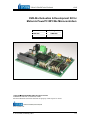
_ v1.0 USERS MANUAL EVB-56x Evaluation & Development Kit for Motorola PowerPC MPC56x Microcontrollers Ordering code EVB-563 ITMPC563 EVB-565 ITMPC565 Copyright 2003 iSYSTEM, GmbH. All rights reserved. winIDEA is a trademark of iSYSTEM, GmbH. All other trademarks used in this document are property of their respective owners. www.isystem.com iSYSTEM, February 2003 1/8 CONTENTS FEATURES ....................................................................................................................... 3 SPECIFICATIONS ............................................................................................................... 3 STANDARD CONFIGURATION ........................................................................................... 3 Options........................................................................................................................ 3 EVB56X FEATURES ......................................................................................................... 3 SOFTWARE DEVELOPMENT .............................................................................................. 3 GETTING STARTED ...................................................................................................... 4 SETTING UP THE EVB-56X BOARD ................................................................................... 4 CONNECTING THE BOARD TO PC...................................................................................... 4 RUNNING WINIDEA......................................................................................................... 4 WHAT TO DO NOW?.......................................................................................................... 4 TROUBLESHOOTING ......................................................................................................... 5 EVB-56x doesn’t show life signs by first start ............................................................ 5 Unable to download the code to the board................................................................. 5 Unable to program the Flash memory........................................................................ 5 MEMORY BANKS AND DEFAULT MEMORY MAP............................................... 6 EVB-56X MEMORY MAP ................................................................................................. 6 Internal Memory ......................................................................................................... 6 External Memory ........................................................................................................ 6 SRAM MEMORY ............................................................................................................. 6 FLASH MEMORY .............................................................................................................. 6 Programming the Flash memory ................................................................................ 7 SETTINGS AND OPTIONS............................................................................................ 7 FLEN JUMPER ................................................................................................................. 7 JTAG PORT ..................................................................................................................... 7 BDM DEBUG PORT.......................................................................................................... 8 NEXUS DEBUG PORT ..................................................................................................... 8 RESET SWITCH ............................................................................................................... 8 STATUS INDICATORS ........................................................................................................ 8 iSYSTEM, February 2003 2/8 Features The EVB56x is an evaluation board for the Motorola series of MPC56x PowerPC microcontrollers. The system is supplied in the package with the on-board MPC56x, 8 Megabit (512 K x 16-Bit) Simultaneous Operation Flash Memory, 4Megabit (256Kx16-Bit) SRAM, debug interfaces, wall plug power source, printed hardware manual and the CD with programming utilities, support software and technical manuals. Specifications Clock 56 MHz Maximum Operating temperature: 0°C to +70°C Power requirement: 6 - 20V DC @ 400 ma Typical Power output: 5V, 3.3V, and 2.6V regulated supplies Board Size: 86 mm x 62 Standard Configuration EVB56x without external memory 230V wall plug power source Printed manual and software on CD. Options • • M External Flash and SRAM option (AM29DL800, TC55V16256) CE Global wall plug power source option EVB56x Features • • • • • • • • 4Mbit (256K x 16) SRAM 8Mbit (512K x 16) Simultaneous Operation Flash EPROM Power Indicators – Supply voltage indications for 3.3, and 2.6V supplies Reset Switch – POR button User Indicator – one user indicator to provide user conceived visual response during testing Configuration jumper- enables/disables internal flash memory Two debug options available – BDM, Nexus Low cost and user friendly support manual and software Software Development The example monitor / utility software initializes the clock to run this board at 20 MHz on powerup. The board has been tested and does run at speeds up to 56 MHz however, which you can set by changing the PLL Register in your software. Software development on the EVB-56x is best performed using a BDM tool connected to the BDM-Port or Nexus connectors. This provides real-time access to all hardware, peripherals and memory on the board. Software is usually uploaded to RAM and executed during development, then programmed into EEPROM to execute when power is applied. BDM software is also available for high-level source code debugging. Contact the manufacturer for more information. iSYSTEM, February 2003 3/8 Getting Started Setting up the EVB-56x board Every development board is tested and loaded with a test code. Test application is loaded into internal Flash, which can be erased ca. 100 times. Therefore it is not recommended to burn the Flash too often. EVB-56x with the option M comes with an external memory. The Code is loaded into external Flash to save the internal Flash. a) Ensure, that the Flash enable FLEN jumper is closed for standard board and open for option M. Connecting the board to PC a) Plug the AC adapter into the wall and connect it to the EVB56x. b) This will power on the evaluation board. Check that power indicators (LD1, LD2) lit and that status LED blinks (MPU heartbeat). c) Connect the board to the emulator through a proper port (BDM, Nexus). If the tools (emulator, POD, winIDEA software) are not installed yet, stop here and setup other tools first. See included manuals. Running winIDEA a) Run winIDEA by selecting Start>Programs>…. b) winIDEA will start up with default project c) Insert the CD with EVB-56x support software into local drive. Go to File>Workspace>Open Workspace and chose the MPC56x.jrf file on support disk. Ensure, that you follow the folders started by emulator and POD types. For example: If you are using the emulator iC3000 with BDM port connected to EVB-563, select the file CDDIR:\EVB56x\Int_Ram\BDM_MPC563.jrf. d) This will configure the winIDEA software with proper setup. e) Go to Hardware>Hardware… menu and select your emulator options. f) You can download the test code to the hardware selecting Debug>Download menu. g) Successful download shall show start location in the code and disassembly window and not report any warnings or errors. h) Run the downloaded application by selecting Debug>Reset And Run. i) Successful operating is indicated with blinking LED LD3. The code is running from internal memory on standard board or from Flash with the option M. What to do now? winIDEA allows you to run code step by step, set breakpoints, examine and modify the source code, change the configuration and much more. For more information refer to the winIDEA documentation. iSYSTEM, February 2003 4/8 Software in the combination with the development board can be used as a basis for developing future applications also on your hardware. This project illustrates various programming issues, which are essential to all winIDEA projects: • • • • • Initialization of bus interface unit Initialization of configuration registers Implementation of dispatch table Format of linker definition file Correct project settings (Project>Settings), which ensure that iSystem tools are invoked successfully More interesting examples are also included on support CD. Troubleshooting EVB-56x doesn’t show life signs by first start a) Check the power supplied to the EVB board – Diodes LD1 and LD2. b) Ensure that FLEN is set accordingly to the EVB version (option M) c) For first start the POD does not need to be connected to the debug port. EVB is shipped with power on bootable test application. The debug port sometimes keeps the device under reset until the connection is established. d) Press the RESET button. e) Try to load the code and run the board through the emulator. Unable to download the code to the board a) b) c) d) e) Check the power supplied to the EVB board Ensure that the debug cable is configured and plugged into proper connector Ensure that FLEN is set accordingly to the EVB version (option M) Ensure that the correct workspace was loaded into winIDEA. Check the hardware configuration: • Tools>Hardware Plug-In • Hardware>Hardware … • Hardware>Emulation Options f) Reset the board and try to connect again Unable to program the Flash memory a) b) c) d) e) Check the power supplied to the EVB board Ensure that the debug cable is configured and plugged into proper connector Ensure that FLEN is set accordingly (On for internal flash, Off for External) Ensure that the correct workspace is loaded into winIDEA. Check the hardware configuration: • Tools>Hardware Plug-In • Hardware>Hardware … • Hardware>Emulation Options • Flash>Setup…. f) Disconnect the power for few seconds and repeat the process iSYSTEM, February 2003 5/8 Memory Banks and Default Memory Map The EVB-56x board provides two memory banks, which can be optionally selected by the MPC5xx microcontroller chip selects. The memory banks are the SRAM (U6)and Simultaneous Operation Flash EPROM (U5). Since the MPC5xx chip selects are fully programmable (with the exception of CS0 providing external Reset start-up) the banks can be located at any location in the MPC5xx memory space. As a reference example, iSystem has defined a default memory map where the chip selects are located at predefined locations. The provided software uses that memory configuration. If you modify the memory map make sure that all memory banks and chip select configuration settings are correct. EVB-56x Memory Map Internal Memory Address Memory Type Range 0000 0000Internal Flash Memory 002F 7FFF (FLEN must be enabled) 002F 8000DEC RAM and Flash Control 002F FFFF Registers 0030 0000Control and Status Registers 003F 7FFF 003F 8000SRAM 003F FFFF For details see the Reference manual. Description Internal Flash memory banks (512KB – 1MB) Burst Buffer Controller and Decompression RAM Registers Registers for internal peripheral circuits 28KB RAM, 4KB Overlay External Memory Address Range 0000 00000007 FFFF 0040 00000047 FFFF 0080 0000- Memory Type Configuration 8Mbit (512K x 16) Simultaneous Operation Flash EPROM (If FLEN = Off) 8Mbit (512K x 16) Simultaneous Operation Flash EPROM (If FLEN = On) 4Mbit (256K x 16) SRAM Base address = 0x400000, Port width = 16 bit, Memory Range = 0x80000, Wait state = 4 Base address = 0x400000, Port width = 16 bit, Memory Range = 0x80000, Wait state = 4 Base address = 0x800000, Port width = 16 bit, Memory Range = 0x080000, Wait state = 2 0087 FFFF SRAM Memory The asynchronous SRAM Memory is implemented with one 256K x 16 memory device. This memory bank must be configured as a 16 bit wide port. It is byte accessible for read or write operations. Asynchronous SRAM memory requires wait states. Flash Memory The Bank U5 contains AM29DL800 type flash device. It must be configured as a 16 bit wide port. Read operations can have either byte either half-word access but write operation must be half-word for proper operations. The device requires wait states when accessed. Refer to the specific device data sheet and sample software provided for configuring the flash memory. Due to iSYSTEM, February 2003 6/8 limited number of Flash erase cycles in the microcontroler (up to 100) it is recommended to use external flash memory for development process. This memory can be used together with the boot code for power on initialization. Programming the Flash memory winIDEA allows you to load code directly into internal or external Flash memory. You have to set memory map in your code accordingly with the target configuration. Demo software has the examples configured for both cases. Load the projects into winIDEA and go to the menu FLASH>Program and push the Start button. This will download the code directly to Flash memory. For more information see the winIDEA users manual. Settings and options The EVB-56x supports the MPU in the extended chip mode only. Boot can be done using either external either internal Flash. The device is selected with the jumper FLEN (Flash enable). After the hard reset the MPU samples the PO configuration and starts the boot process accordingly to the settings. FLEN Jumper (OPEN) Boot from external memory (CLOSED) Boot from internal memory The development tool can be connected to the board through two debug ports – BDM and Nexus. Only one can be selected at time. Port selection is done automatically with the proper signaling. No manual settings are necessarily. JTAG Port 1 2 9 10 Pin 1 2 3 4 5 6 7 8 9 10 Signal Name EVB565 EVB563 TDI TDI GND GND TCK TCK GND GND TDO TDO GND GND TMS TMS JTAG compliance Not connected +3.3V +3.3V DBPC JTAG enable JTAG is primarily used for the manufacturing testing and is by default disabled. (JTAG enable and DBPC are low). Port can be enabled with jumper wires on the cable connector. Hard reset is needed for the initialization. Signal JTAG compliance on EVB565 must be high. iSYSTEM, February 2003 7/8 BDM Debug Port 1 2 9 10 Signal Name EVB565 VFLS0 SRESET* GND DSCK GND VFLS1 HRESET* DSDI +3.3V DSDO Pin 1 2 3 4 5 6 7 8 9 10 The development tool (iC3000 for example) selects the port automatically. BDM port is configured after HRESET* transition when the DSCK signal is high. Eight clocks after the MPU samples the DSDI signal to select the mode (high – asynchronous). NEXUS Debug Port Pin 1 2 3 4 5 6 7 8 9 10 Signal Name +2.6V +2.6V KAPWR NC NC NC HRESET* +2.6V EVTI* GND Pin 11 12 13 14 15 16 17 18 19 20 Signal Name RSTI* GND MSEI* GND MDI0 GND MCKI GND MDO0 GND Pin 21 22 23 24 25 26 27 28 29 30 Signal Name +2.6V GND BG*/VF0 GND MSEO* IRQOUT* MDO1 GND MDO2 GND Pin 31 32 33 34 35 36 37 38 39 40 Signal Name MDO3 GND MDI1 GND IRQ/SGPIO GND MDO4 GND MDO5 GND Pin 41 42 43 44 45 46 47 48 49 50 Signal Name MDO6 GND MDO7 GND NC GND NC GND B0EPEE GND Similar as above for BDM port - Nexus port is fully configurable. Development tool (iC3000) configures the port automatically. Low EVTI* enables the Nexus port. The information is sampled with positive RSTI* transition. Port mode – full or reduced depends on MDI0 state. See MPC 56x reference manual for more details. RESET Switch EVB56x board has a power on reset switch, which can be used, when the boot initialization is required. Status Indicators Two LED diodes show the presence of supply voltages. Both LD1 (+3.3V) and LD2 (+2.6V) must light when the power is applied to the evaluation board. Third LED diode (LD3) is available for the user as a status indicator. For example- it can show that the application code is operational. The diode is connected to the MPU pin PCS0/SS*/QGPI0 and will lit when the output is low. iSYSTEM, February 2003 8/8