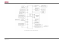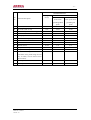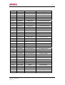
1
Colour TV
Service Manual
-2 -
01
anyo SS01
s: SSanyo
hassiis:
C
Chas
Model: 21SWS1/BN
Model No.: 21SWS1_BN
Version: 1.0
-3 -
CONTENTS
SAFETY INSTRUCTION........................................................................................................................ 4
SPECIFICATION..................................................................................................................................... 8
KEY ICS & ASSEMBLIES...................................................................................................................... 9
SIGNAL PROCESS ............................................................................................................................... 10
SYSTEM BLOCK DIAGRAM.............................................................................................................. 21
IC DATA & SERVICE DATA ................................................................................................................ 24
CIRCUIT ADJUSTEMENT................................................................................................................... 37
SERVICE MODE & BUS DATA........................................................................................................... 43
TROUBLE SHOOTING FLOW CHART.............................................................................................. 48
PART LIST ............................................................................................................................................. 50
CIRCUIT BOARD DIAGRAMS ........................................................................................................... 65
EXPLODED VIEW................................................................................................................................ 69
Model No.: 21SWS1_BN
Version: 1.0
-4 -
SAFETY INSTRUCTIONS
Warning: Before servicing this chassis, read the “X-Ray radiation precaution”, “Safety precaution”
and “product safety notice” instructions below.
X-RTY Radiation precaution
1.
The EHT must be checked every time the TV is serviced to ensure that the CRT does not
emit X-ray radiation as result of excessive EHT voltage. The nominal EHT for this TV is
24.5KV (for 21” CRT only) at zero beam current (minimum brightness) operating at AC
220V. The maximum EHT voltage permissible in any operating circumstances must not
exceed 30KV. When checking the EHT, use the High voltage check procedure in this manual
using an accurate EHT voltmeter.
2.
The only source of X-ray in this TV is the CRT. To prevent X-RAY radiation, the
replacement CRT must be identical to the original fitted as specifies in the parts list.
3.
Some components used in this TV have safety related characteristics preventing the CRT
from emitting X-ray radiation. For continued safety, replacement component should be made
after referring the PRODUCT SAFETY NOTICE below.
SAFETY PRECAUTION
1.
The TV has a nominal working EHT voltage of 24.5KV. Extreme caution should be
exercised when working on the TV with the back removed.
a.
Do not attempt to service this TV if you are not conversant with the precautions and
procedures for working on high voltage equipment.
b.
When handling or working on the CRT, always discharge the anode to the TV
chassis before removing the anode cap in case of electric shock.
c.
The CRT, if broken, will violently expel glass fragments. Use shatterproof goggles
and take and take extreme care while handling.
d.
2.
Do not hold the CRT by the neck as this is a very dangerous practice.
It is essential that the maintain the safety of the customer all power cord forms be replaced
exactly as supplied from factory.
3.
Voltage exits between the hot and cold ground when the TV is in operation, Install a suitable
transformer of beyond rated overall power when servicing or connecting any test equipment
for the sake of safety.
4.
Replace blown fuses within the TV with the fuse specified in the parts list.
Model No.: 21SWS1_BN
Version: 1.0
-5 -
5.
When replacing wires or components to terminals or tags, wind the leads around the terminal
before soldering. When replacing safety components identified by the international hazard
symbols in the circuit diagram and part list, it must be the company-approved type and must
be mounted as the original.
6.
Keep wires away from high temperature components.
PRODUCT NOTICE
Many electrical and mechanical components in this chassis have special safety-related characteristics.
These characteristics are often passed unnoticed by a visual inspection and the X-ray radiation
protection afforded by them cannot necessary be obtained by using replacements rated at higher
voltages or wattage, etc. Components which have these special safety characteristics in this manual
and its supplements are identified by the international hazard symbols in the circuit diagram and part
list. Before replacing any of these components read the parts list in this manual carefully. Substitute
replacement components which do not have the same safety characteristics as specified in the parts
list may create X-ray radiation.
PRECAUTIONS
High voltages are used in the operation of this
television receiver. Do not remote the Cabinet
back from your set. Refer servicing To qualified
service personnel.
To prevent fire or electrical shock hazard. Do not
expose the television receiver to rain or moisture.
Model No.: 21SWS1_BN
Version: 1.0
-6 -
Avoid exposing the television
receiver to direct, Sunlight
and other source of the heat.
Do not stand the television
receiver directly on other
produces, which give off heat
E. g. video Cassette players.
Audio
amplifiers. Do
not
block the ventilation holes in
the back cover. Ventilation is
essential to prevent failure of
electrical component. Do not
squash power supply cord
under the television receiver.
If the television is to be built
into
a
similarly
compartment
enclosed
or
The
minimum distances must be
maintained. Heat build-up can
reduce the service life of your
television, and can also be
dangerous.
Never stand on, lean on push
suddenly the television or its
stand. You should pay special
attention
children.
Model No.: 21SWS1_BN
Version: 1.0
to
children
to
-7 -
Do not place your television on an unstable cart
stand, shelf or table. Serious injury to an
individual, and damage to the television, may
result if it should fall.
When the television receiver is not used for an
extended period of time, it is advisable to
disconnect the AC power cord from the AC outlet.
MAINTENANCE
1.
Use a piece of soft cloth when cleaning. (Neutral detergent is allowed.) Never use thinner or
2.
To ensure safety, unplug the TV set when cleaning.
3.
Do not turn on the TV set in thundery days. At lightning intervals, pull off the power cord
volatile, etc.
and the antenna cable.
4.
Vacuum cleaner is recommended to clean the dust stick to the window net.
5.
Do not put magnetic objects near the TV set to avoid color distortion.
6.
Avoid hitting screen with hard objects. Attention when handling and transporting.
Warning!
There are no repairable components inside this set. Do not try to make any change to it. High voltage
inside may cause danger.
Model No.: 21SWS1_BN
Version: 1.0
-8 -
SPECIFICATION
Model Number
21S01
RF system
Color system: PAL, NTSC3.58, NTSC4.43
Sound system: D/K, I, M, B/G
Video system
PAL, NTSC3.58, NTSC4.43 (50/60Hz)
Receiving channel
VHF: C1 ~ C12
UHF: C3 ~ C57
CATV: Z1 ~ Z37
Programs preset
255
Antenna input
75Ω (unbalanced)
Audio output
5W (THD ≤7%)
Power source
150 – 250V AC, 50/60Hz
Weight (Approx)
25Kg
Rated power consumption (AC 220V 50Hz)
75W
Designs and specifications are subject to change without notice.
Model No.: 21SWS1_BN
Version: 1.0
-9 -
KEY ICS AND ASSEMBLIES
Serial No.
Position No.
Type
Function Description
1
N101
LA76818A
Small signal processor
2
N451
TDA9302
Vertical output circuit
/LA78040
3
N601, N602
LA4285 /LA4287
3W /5W sound power amplifier
4
N701
LC863328B-52G5
System control micro processor
5
N801
CD4053BE
Audio /video switch circuit
6
N551
L7809CV
Tri-pin regulator
7
N702
ST24C08
EEPROM
Model No.: 21SWS1_BN
Version: 1.0
-10 -
SIGNAL PROCESS
1.
HIGH /INTERMEDIATE FREQUENCY SIGNAL PROCESSOR
Through the high /intermediate frequency signal processor, the RF TV signal received by the
antenna is high-frequency amplified and converted to develop and output an IF signal, then are IF
amplified and demodulated to develop a video signal and SIF signal as well as AFT control signal
and AGC control signal. The high /intermediate frequency signal processor mainly consists of a
A101 tuner, IF filtering circuit formed of V102 and Z101 and IF signal processor in LA76818A.
If signals output from the A101 tuner are coupled by C110 to V102 IF pre-amplifier for IF
amplifying by about 20dB to compensate insertion loss of Z101 SAW filter. After coupled by
C112, the IF signals output from V102 are sent to the Z101 SAW filter to develop IF signals,
which meet requirements for the IF and amplitude frequency characteristics, to N101’s Pin5 and
Pin6. In N101, the generated IF signal are filtered out a video signal as a second SIF signal after
through multi-polarity IF amplifying and PLL sync detecting, which then are output in two ways.
After one set of signal is trapped (to eliminate the second SIF signal), cored and pre-video
amplified, Pin 46 outputs video signals, which are sent to the video circuit for processing from
N101’s Pin44 after divided by R201 and R202 and coupled by C204, another set is output from
N101’s Pin52, which is later sent to the SIF circuit from N101’s Pin54 after coupled by C126.
The band control voltages of the A101 tuner are controlled respectively by levels output from
Pin41 and Pin42 of N701 output low level to supply band switchover voltage to related pin of the
tuner after out-phased by the related triode.
N701’s Pin8 supplies VT voltage to the A101 tuner. The width pulse output from N701’s Pin8 is
converted into DC tuning voltage to be supplied to VT terminal of the tuner after level-converted
and out-phased by V701 and integrating filtered by C707, R710, R712, R714, R715, R716, C709,
C711, R718, N705 and C 708 are formed into a 33V stabilizing circuit.
The RF AGC voltage from LA76818’s Pin4 is sent to AGC control terminal of the tuner through
R104, R103 and R119 are voltage-dividing bias resistors of RF AGC and C104 is a filtering
capacitor.
Model No.: 21SWS1_BN
Version: 1.0
-11 -
In the IF filtering circuit V101, VD101, R116, R117, R106, R112 and R115 are formed into an IF
absorption selection circuit, which is controlled by the level from N701’s Pin35 output high level,
V101 saturates and conducts, and R106 is integrated into the paralleled resonator comprising
R112 and VD101, by which the resonating frequency dot is moved to low frequency section and
IF and amplitude frequency characteristics are stretched. In this case, IF characteristics are
stretched. In this case, IF characteristics include B/G, I and D/K SIF characteristics. When Pin35
output low level, V101 cuts off and VD101 is not integrated into the paralleled resonator, by
which the resonating frequency dot is moved to high frequency section and IF and amplitude
frequency characteristics are narrowed. In this case, IF characteristic includes M SIF
characteristic.
In the IF pre-amplifier, R108, R109 and R111 are bias resistors of V102, R107 and C111 are
formed into a decoupling filter circuit, R110 is a damping resistor to stretch frequency band of
the amplifier.
2.
VIDEO SIGNAL PROCESSOR
The video signal processor in LA76818A mainly consist of an AV switch and filtering circuit,
luminance signal processor, chroma signal processing/ color decoding /RGB selection circuit,
which is mainly used to complete all video signal processes and demodulate out three primary
color signals R, G, and B.
a)
TV /AV switch circuit in LA76818A is used for switching over TV video signals,
AV video signals, Y/C signals from the S-VHS terminal. The filtering circuit is used
for strobe, delay, sharpness control, black level stretching for Y signal and strobe,
amplification, color saturation control and color killing control for C signal.
The video signals from LA76818A’s Pin46 are coupled by C204 to Pin44. External
video signals from the AV terminals are coupled by C211 to Pin42. After clamped,
DC video signals are restored and sent into the TV /AV switch circuit to select out
one set of video signals from the internal video signals under the control of the I2C
bus. Then the set of video signals are output in three ways. One set is output from
LA76818A’s Pin40 and sent to the video output terminal after divided by R802 and
E804, buffered by V801 and coupled by C805 to provide video signal source for the
monitor. Another two sets of signals are sent to the filtering circuit for Y /C
separation.
Model No.: 21SWS1_BN
Version: 1.0
-12 -
All the color trap in the luminance channel, band pass filtering circuit in the chroma
channel and filter adjuster are controlled by the broadcast system identifying circuit
and I2C bus to ensure correct and complete Y /C separation when different-system
signals received. Meanwhile, when Y /C separation signals are input to LA76818A’s
Pin44 and Pin42, the inner I2C bus makes the color trap in the luminance channel
and band pass filtering circuit in the chroma channel enter the bypass mode, thus
preventing attenuation to signal to the greatest extent and ensuring sharper and
more vivid pictures.
b) Luminance signal processor
The luminance signal processor includes a luminance delay line, definition control
circuit, coring circuit and contrast /luminance control circuit.
As the bandwidth of channel processing the luminance signal is wider than one
processing the chroma signal, the transmission speed of the luminance signal is
faster than of the chroma signal. It without delay processing, the time when the
luminance signal reaches the CRT is not consistent with that when chroma signal
reaches the CRT, resulting in display luminance and color not coinciding. A
luminance delay line integrated in LA76818A can adjust delay time of the delay
line by the I2C bus so that the luminance and chroma signals reach the CRT
synchronously. After delay processed, the luminance signal is sent into the
definition control circuit, coring circuit, black level stretcher and contrast/
luminance control circuit for processing, and then sent into the luminance amplifier
for amplifying and outputting a Y signal to the primary color matrix circuit.
LA76818A is equipped with an aperture compensating circuit to improve definition
of pictures, coring circuit to reduce high frequency noise and black level stretcher to
improve picture quality greatly.
c)
Chroma signal processor
The chroma signal processor includes an ACC amplifier, killer identification control
circuit, sub-carrier restorer, base band delay circuit, PAL /NTSC demodulator and
color difference matrix /primary color matrix circuit.
The video signals selected out by the video switch are filtered out chroma signals
with luminance element removed by the band pass filter, which are sent to the
chroma signal selector. After selected, the chroma signals are amplified and
chroma-controlled by the ACC circuit, and then output in two ways. One set is sent
chroma demodulator and another set to sub-carrier restorer.
Model No.: 21SWS1_BN
Version: 1.0
-13 -
To correctly process chroma signals, firstly identify the input chroma signals. The
I2C bus controls LA76818A to identify chroma signals. To identify chroma signals,
identify signal systems and subcarrier frequency.
For NTSC signals, the subcarrier modulated by two color difference signals will not
be progressively out-phased while the subcarrier modulated by R-Y color different
signal PAL will be progressively out-phased. So whether the subcarrier phase
modulated by R-Y signal or phase of color sync signal is out-phased or not decides
that the signal is in NTSC or PAL system.
Both NTSC and PAL signal have a dual-frequency subcarrier, I.E. 4.43MHz and
3.58MHz. After detecting out two subcarrier frequencies at the same time of
detecting subcarrier phase, the corresponding 4.43MHz or 3.58MHz can be
identified (PAL4.43 and NTSC3.58 are standard systems while PAL3.58 and
NTSC4.43 are nonstandard).
The subcarrier restorer in LA76818A uses a 4.43MHz crystal (G201) externally
connected to N101’s Pin38 as an oscillating source to generate a 3.58MHz or
4.43MHz dual-frequency subcarrier.
VC01 is a crystal oscillator with high Q value and narrow oscillating range. VC02
is an inner oscillator with wide oscillating range. Firstly, oscillating signals
generated from VC02 and VC01 are discriminated in APC2, then the generated
error signal is filtered by the filtered by the filtering circuit externally connected to
LA76818A’s Pin36 to get consistent oscillating frequencies of VC02 and VC01.
Secondly, the oscillating signals are sent to APC1 by the tint adjuster to be
discriminated together with the chroma signal from ACC. The error signal
generated from the phase discriminator is filtered by the circuit externally
connected to Pin39 to control oscillating frequency of VC02 so that it is consistent
with chroma subcarrier frequency from ACC. Taking the calibrated subcarrier
regeneration signal as reference, further calibrate oscillating frequency of VC02 in
the APC2 circuit. Only after the APC2 circuit discriminates twice, can it correctly
calibrate subcarrier regeneration signal of one frequency (firstly calibrate subcarrier
regeneration signal on oscillating frequency of VC01; secondly recalibrate on
subcarrier frequency of received chroma signal through VC01).
The calibrated sub-carrier regeneration signal is sent into the decoder through the
PAL switch to demodulate out R-Y and B-Y color difference signals together with
the modulated signal from ACC.
Model No.: 21SWS1_BN
Version: 1.0
-14 -
The demodulated color difference signals are sent into the color difference signal
selector after clamped by the clamper. If with SECAM demodulation function, the
circuit also sends color difference signals output from the SECAM demodulator to
the color difference signal selector from Pin34 and Pin36. Under the control of the
I2C bus, the color difference signals selected by the selector are sent to the base
band delay line and adder respectively for further processing.
With PAL signal received, the circuit correct color phase distortion by means of
progressively out-phasing R-Y color difference signals, causing tint distortion.
Crosstalk may exit between the two color difference signals after simple PAL
demodulation. Therefore, PAL signals should be color-difference-signal separated
by the 1H base band delay circuit.
The color difference matrix /primary color matrix circuit includes a matrix circuit to
generate a G-Y signal, contrast /luminance control circuit, primary color matrix
circuit, character clamper, character contrast control circuit, primary color selector,
white balance adjuster and beam current control circuit. The R-Y and B-Y color
difference signals from the base band delay circuit are sent to the color difference
matrix circuit for matrix processing to get a G-Y signal. The three color-difference
signals are sent to the contrast /luminance control circuit together with the Y signal.
Before sent to the primary matrix, the color difference signals/Y signal should be
unitedly adjusted by the contrast /luminance control circuit to get proper three
primary colors. In addition, LA76818A is equipped with setup circuit for
sub-brightness, sub-contrast and sub-saturation so that users can adjust brightness,
contrast and saturation, all of which are controlled by CPU through the I2C bus.
The R-Y, B-Y and G-Y color difference signals can be processed into R, G and B
three primary color signals after together with the Y signal in the primary color
matrix circuit, which function as drive signals to display main pictures. Send the
three primary color signals and the three character primary color signals from the
CPU into the primary color selector for selection, then output.
The three character primary color signals from the CPU are input to Pin14, Pin15
and Pin16 of LA76818A respectively. Firstly, clamp them on a fired DC level to
restore out the DC element lost during AC coupling transmission. Secondly, send
the signals to the character contrast control circuit. Under normal condition,
characters are slightly brightly than picture while the former changing range is
narrower than the latter. The character blanking signal is input to Pin17 of
LA76818A. When the signal is abnormal. No character display may appear.
Model No.: 21SWS1_BN
Version: 1.0
-15 -
d) White balance adjuster
Traditional white balance is adjusted through adjusting the bright and dark balance
potentiometers of the CRT drive circuit. The white balance adjuster of the chassis is
equipped in LA76818A, which is performed by the CPU through the I2C bus.
e)
Video amplifier
The video output circuit is amplify three primary colors and drive the CRT to
display color pictures.
V902, V912 and V922 are three end video amplifying triodes. V931, V932, VD901,
VD911, VD921, C901, C911 and C921 are formed into a spot killer.
When the TV operates, 9V supply voltage supplies enough voltage to C932 so that
C905’s negative has lower potential to saturate V931 and its positive has higher
potential to cut off V932. as the positive potential of VD901, VD912, VD922
diodes lower than their negative potentials, the diodes cut off, not affecting the TV’s
operation. When turn-off, C931, C932 and C933 discharge to cut off V932 through
VD902, VD903 and R933, as the electric charge of C934 is discharged quickly due
to its too small capacitance, V932’s emitter is conducted to conduct VD901, VD911
and VD921, ensuring V902, V912 and V922 end video amplifying triodes
conducting for a period of time and high voltage of the CRT discharged quickly
through the end amplifying triodes. Thus spot is killed when turn-off.
3.
AUDIO SIGNAL PROCESSOR
The audio signal processor mainly consists of a SIF processor, audio switchover circuit and audio
power amplifier. 21S01 uses LA4287 to complete audio power amplifying.
a)
SIF processing and audio switchover circuit.
The detected video signal as well as second SIF signal is output from Pin52 of
LA76818A to be coupled by R122, from which the high pass filter including C125,
C126 and L121 filter out a SIF signal y to be sent to the band pass filter connected
to Pin54. The band pass filter further filters interference elements except
4.5-6.5MHz SIF signals out of the two signals for sent to phase discriminator. In
addition, SIF carrier signal from the SIF carrier signal from the SIF carrier PLL
restorer (SPLL) is also sent to the phase discriminator. After the discriminator
compares the two signals, the filter externally connected to Pin53 filters high
frequency element out of the generated error signal and processes it into DC error
voltage to control oscillating frequency in the SPLL circuit so that the frequency is
always consistent with the received sound IF.
Model No.: 21SWS1_BN
Version: 1.0
-16 -
In the SPLL circuit, the frequency at which a SIF carrier signal is developed ranges
from 4.5M to 6.5M which is used for demodulating M, B/G, I or D/K SIF signal is
received, firstly perform discrimination adjustment mentioned above and calibrate
the SIF carrier generated from SPLL. Then lock the SPLL oscillating circuit onto
the calibrated frequency. The output SIF carrier signal is sent to the frequency
discriminator for frequency discrimination. The output SIF carrier signal is sent to
the frequency discriminator for frequency discrimination.
The SIF signal filtered by the double-level band pass filter is cut off a parasitic AM
signal after amplified by the amplitude limiter, which is later sent into the FM
frequency discriminator together with the SIF carrier signal to demodulate out an
audio signal, then in two ways. One of set output from LA76818A’s Pin1 to the AV
terminals through V802 follower, another set is directly sent to the switchover
switch to be switched over with the audio signal input to the AV terminals at N801’s
Pin1, Pin2, Pin3, Pin5 and then output from the Pin4, Pin 15 to the audio power
amplifier after through DC volume control under the control of the N701 Pin5,
Pin6.
b) Audio power amplifier.
The audio power amplifier comprises LA4287 (for 21S01). The following give
descriptions of the circuit on basis of LA4287.
An audio signal from LA76818A’s Pin 1 and Pin4, Pin15 is coupled by C611, C621,
voltage divided by R611, R612, coupled to L601’s Pin3 and L602’s Pin3. After
audio-power-amplified by LA4287, the signal is output from Pin 9 to drive the
speakers to output sound V631, V632 and V633 are formed into a mute circuit.
4.
HORIZONTAL /VERTICAL SCAN CIRCUIT
The horizontal /vertical scan circuit in this chassis comprises a sync separator, horizontal
oscillator, horizontal /vertical frequency divider, 50Hz /60Hz identifying circuit, AFC1 /AFC2
and line pre-drive circuit in LA76818A; V431 line drive circuit, V432 horizontal output circuit
and LA78040 /STV9302 vertical output circuit.
a)
LA76818A horizontal /vertical scan small processor
LA76818A applies a digital dividing horizontal /vertical scan circuit. In the circuit a
4MHz oscillation signal generated from the crystal oscillator is processed into a
horizontal frequency square wave signal by the frequency divider and AFC1 and
AFC2 circuits, which later is divided to develop a vertical frequency pulse signal.
The circuit improves sync performance greatly with low horizontal start voltage
(5V) and without horizontal sync and vertical sync adjustments.
Model No.: 21SWS1_BN
Version: 1.0
-17 -
In addition, LA76818A can automatically control operating mode of the vertical
output circuit by means of the I2C bus signal with 50/60Hz vertical frequency auto
identifying circuit built-in, ensuring picture’s vertical size unchanged with 50Hz or
60Hz vertical frequency.
b) Sync separator
The sync separator in LA76818A consists of a horizontal sync separator (including
a sync separation triode T and comparison amplifier 1) and vertical sync separator.
The bias of T1 is supplied with 7V fired bias voltage, with sync chip (downwards)
in the video signal. Potential of T1’ emitter drops and the emitter conducts. The
conducted current charges the internal capacitor C through T1 with positive to the
upper and negative to the lower. Without sync chip, potential of T1’s emitter rises
and the emitter cuts off, thus the collector outputting high level to get negative pulse
with the same width as the sync chip’s on the T1’s collector and separate out a
composite sync signal. At the same time, C discharges slowly through R1 to get
ready for the next sync separation.
The negative sync pulse separated by the T1’s collector is out-phased to positive
pulse by the comparison amplifier 1, which is output in three ways. The first set is
sent to the AFC1 PLL discriminator to function as a reference phase signal. The
second set is separated out vertical frequency pulse by the vertical sync separator
and shaped into vertical sync pulse with steep edges to be sent to the vertical divider.
The third set is supplied to the horizontal consistency detector for checking
horizontal scan for sync.
c)
Horizontal oscillator
The horizontal oscillator in LA76818A is a integrated voltage-control oscillator
whose free oscillating frequency is 256xfH=4MHz. Different from conventional
integrated horizontal scan oscillator, the horizontal frequency oscillator in
LA76818A only needs to be externally connected to a error resistor with smaller
reference current source of the inner horizontal oscillator.
d) AFC1 PLL discriminator and horizontal frequency divider
AFC1 PLL discriminator in LA76818A includes A voltage-control crystal oscillator,
horizontal frequency divider, phase discriminator 1 and AFC1 low-pass filter
externally connected to Pin26. The discriminator is a frequency phase lock loop
circuit, whose reference signal comes from horizontal sync pulse output from the
comparison amplifier 1.4MHz oscillation signal generated from the horizontal
oscillator in LA76818A is sent to the horizontal divider, which is sent to horizontal
count frequency divider after fixedly divided with 256 times the size of horizontal
frequency.
Model No.: 21SWS1_BN
Version: 1.0
-18 -
As the chassis can receive multi-system signals, horizontal scan frequency differs
dependent on different-system TV signals. To make the horizontal oscillating signal
in the horizontal counting frequency divider, which are controlled by the CPU
through the I2C bus. The CPU counting divider to count up or count down and
counting amount according to size and direction of the phase. Discrimination error
in the AFC1 circuit. After comparing the pulse from the counting divider to that of
the received horizontal sync signal in AFC1, the error current is generated, which is
processed into DC error voltage by the RC low pass filter externally connected to
Pin26 to control horizontal oscillation and adjust oscillation frequency of VCO. If
the two pulses are the same, counting adjustment stops to lock the loop so that
frequencies of two-way input signals from AFC1 equal.
e)
AFC2 discriminator and phase shifter
In LA76818A, the second group PLL formed of AFC2 circuit and horizontal output
phase control circuit (phase shifter) is to correct phase of horizontal frequency pulse
output from Pin27.
AFC2 has two sets of signals input: one set of signal is a horizontal frequency
square wave pulse from the frequency divider functioning as a reference signal for
the frequency and phase of the horizontal frequency pulse is locked in AFC1 by the
horizontal sync pulse and remains unchanged. After delayed for about 4µs (to
compensate delay resulted from horizontal output circuit for convenience of locking
loop), the signal is sent to the AFC2 circuit.
Another is a horizontal flyback pulse output from T471 GBT. The pulse is sent into
the IC from Pin28 of LA76818A to be pulse shaped into a pulse signal with steep
locked edges, which is sent into the AFC2 circuit as a comparison signal. Through
phase comparison, the two signals are processed into error current, which later is
filtered out to DC error voltage by IC’s low pass filter to control phase-shift angle
and adjust horizontal frequency pulse phase output from Pin28, thus controlling
start time of horizontal flyback and positive /negative peak of the horizontal scan
current and correcting positive conducting time and current peak value of horizontal
output triode.
In addition, LA76818A horizontal scan small signal processor can also output
4MHz horizontal oscillation signals and sandcastle pulse which function as clock
signals and horizontal sequence control of the SECAM decoder. LA76818A’s Pin30
functions as the 4MHz clock output terminal (AC grounding).
Model No.: 21SWS1_BN
Version: 1.0
-19 -
f)
Vertical divider
The horizontal frequency oscillation pulse from the horizontal scan count divider is
sent to the vertical count divider. Meanwhile the vertical sync signal from the
vertical sync separator (frequency separator) is also sent to the vertical count divider.
Controlled by the vertical sync pulse, the circuit counts horizontal frequency pulses
and identifies and correct vertical frequency, all of which are controlled by the CPU
through the I2C bus. The vertical frequency is shifted to the Capture, Identification
or Locking mode by the CPU.
Capture mode: The vertical sync count divider enters the wide-range count
comparison mode, in which the CPU provides a wide-range count comparison value,
i.e. when vertical frequency of the received signal changes within a wide range, the
count circuit can always pause counting and enters another mode for counting and
comparing.
Identification mode: Once the count circuit pauses counting in the Capture mode,
the CPU provides a relatively narrow-range of count comparison value and the
count divider recounts and re-compares until the comparison is finished to enter the
Locking mode.
Locking mode: After identification, the CPU provides a narrower-range of count
comparison value. Only when vertical frequency of the received signal changes
within a very narrow range, can the operation mode be changed and enter the wide
hold range, ensuring the generated vertical drive pulse strict with the vertical sync
pulse.
g) Vertical sawtooth generator and vertical output circuit
The vertical frequency pulse output from the vertical count divider is sent to the
sawtooth generator to develop a sawtooth with corresponding vertical frequency,
which is output from LA76818A’s Pin23 to the vertical output circuit. To get stable
amplitude of the locked vertical frequency sawtooth signal, an auto level limiter
(ALC) is also integrated in LA76818A to control amplitude of the output sawtooth.
Externally connect the ALC’s filtering component to Pin24 of LA76818A. The
chassis’ vertical output circuit consist of LA78040.
The vertical frequency sawtooth from LA76818A’s Pin23 is DC coupled by R451 to
LA78040’s Pin1 to be amplified by the internal differential amplifier. Pin7 is an
in-phase input terminal of the differential amplifier. Externally connected R453 and
R454 are DC bias resistors, and C454 is a filtering capacitor. In the chassis, the
in-phase input of the differentiate amplifier is fixed to reference potential of the DC
Model No.: 21SWS1_BN
Version: 1.0
-20 -
amplifier. The amplified vertical sawtooth voltage is output from Pin5 to the
deflection yoke to generate deflection current. R452 and C459 filter out of
horizontal frequency element inducted by the horizontal scan circuit. R460 and
C458 eliminate parasitic oscillation generated when the deflection yoke and
distributed capacitors resonate. The branch formed of C456, R458 and R459 fetches
out an AC sawtooth from lower part of the deflection yoke to be fed back to the
input terminal to correct vertical scan linearity. R455, R456, R457 and R459 are
formed into a DC voltage divider to fetch out DC voltage to feed back the input
terminal to regulate DC operating point of the output stage. C453 is a high
frequency decoupling capacitor. VD450 and C452 are formed into a pump supply
voltage raiser. The vertical flyback pulse output from Pin3 us used for positioning
characters.
h) Line drive and horizontal output circuit
Similar to that of conventional TVs the line drive and horizontal output circuit
comprises discrete components including a line drive triode V431, horizontal output
triode V432, line drive transformer T431 and FBT T471.
LA76818A’s Pin27 output line drive pulse with of 24µs, which is supplied to base
of V431. After amplified and pulse shaped by V431 and coupled by T431, the
horizontal frequency pulse is supplied to base of V432. R433 and C433 are formed
into a damping resistor to restrict primary of T431 form generating large-amplitude
inductive electric potential and avoid breakdown of the line drive triode. C433 is a
high frequency filtering capacitor to remove high harmonic.
Line drive pulse from the secondary of T431 line drive transformer is supplied to
base of V432 to control V432 operation and develop sawtooth scan current in the
horizontal deflection yoke so that electron beams in CRT scan horizontally and over
1KV horizontal flyback pulse is formed on collector of the V432.
C435 and C436 are flyback capacitor. Adjusting their capacitances properly can
change horizontal flyback time L431 and L432 are used to restrain horizontal
radiation. DY-H is a horizontal deflection yoke. C441 are S correcting capacitors,
L441 are linear correcting inductors and R441 are dampening resistors.
The flyback pulse from T471’s Pin6 provides filament voltage for the CRT through
R930. The horizontal flyback pulse from Pin4 is supplied to the CPU to position
character level after out-phased by V705 or supplied to N101’s Pin28 for AFC
discrimination. In addition, T471 provides focus voltage, screen voltage and anode
high voltage for the CRT.
Model No.: 21SWS1_BN
Version: 1.0
-21 -
SYSTEM BLOCK DIAGRAMS
Model No.: 21SWS1_BN
Version: 1.0
-22 -
Model No.: 21SWS1_BN
Version: 1.0
-23 -
Model No.: 21SWS1_BN
Version: 1.0
-24 -
IC DATA AND SERVICE DATA
LA76818A SMALL SIGNAL PROCESSING CIRCUIT
1.
Features
LA76818A is a multi system color TV specific monolithic IC developed by SANYO Co. in 2002,
which is controlled by the I2C bus. LA76818 comprises a tuning circuit and all small signal
processing circuit including a PIF /SIF /luminance and chroma signal processing circuit, PAL
/NTSC processing circuit, RGB signal processing and controlling circuit, horizontal /vertical
small signal processing, SIF processing and demodulating circuit and volume controlling circuit.
It has following features.
Multi system IF processing, high-gain IF amplifier and AGC without adjustment
needed except IF phase-locked VCO coil. A buss eliminator is also built-in the IC.
Video PLL detector improves video detection characteristic and picture /sound
quality greatly.
Video /audio switchover switch built-in.
Built-in luminance delay line, aperture correcting circuit, coring circuit and black
level stretching circuit improve picture quality greatly.
Color signal trap and band pass filter, skin tone control circuit and white balance
auto adjusting circuit built in.
Analog OSD and RGB switchover control circuit built-in with fast RGB blanking.
The horizontal /vertical scanning circuit uses dual auto frequency adjustment,
50/60Hz auto decision with constant vertical picture when no signal received.
SECAM signal decoding offers together with LA7642N
In addition, LA76818 features also sandcastle pulse generation, SECAM control clock output, PWM
pulse width modulation and control.
Model No.: 21SWS1_BN
Version: 1.0
-25 -
2.
Block diagram
Model No.: 21SWS1_BN
Version: 1.0
-26 -
LA4285 3W POWER AMPLIFIER AND STEREO
1.
Feature
TV sound output
Exchangeable with LA4285 (3W) /LA4287 (5W) pin
Package SIP-10HD (Pitch=2.54mm, straight type)
Heat protection loop and over voltage protection loop built in
Power output: 3W (Vcc=19V /RL=8Ω) LA4285
5W (Vcc=22V /RL=8Ω) LA4287
2.
Diagrams
Model No.: 21SWS1_BN
Version: 1.0
-27 -
3.
Refer to table 5 about functions and data of the LA4285’s Pins
Model No.: 21SWS1_BN
Version: 1.0
-28 -
LA78040 /STV9302 (N451) VERTICAL DEFLECTION OUTPUT CIRCUIT
1.
Features
Low power dissipation due to built-in pump-up circuit
Vertical output circuit
Thermal protection circuit built in
Excellent crossover characteristics
DC coupling possible
Feature
Power amplifier
Flyback generator
Output current up to 2 App
Thermal protection
Description
The STV9302 is a vertical deflection booster designed for monitor and TV applications.
This device, supplied with up to 32V, provides up to 2App output current to drive the vertical
deflection yoke.
The internal flyback generator delivers flyback voltage up to 60V.
PIN CONNECTION (Top view)
Model No.: 21SWS1_BN
Version: 1.0
-29 -
2.
Block diagram
3.
Refer to table 6 about functions and service data of LA78040’s Pins
Model No.: 21SWS1_BN
Version: 1.0
-30 -
Table 2 functions and service data of LA76818A (N101)’s Pins
DT890D Multimeter
Voltage of
Pin
No
Function Description
Pin (V)
Ground Resistance (Ω)
Measure with Red
Measure with
Probe while
black Probe while
grounding Black
grounding red
probe.
probe
2.44 /2.28
810
712
1
Audio signal output
2
Audio frequency discrimination output
2.34
975
675
3
IF AGC filter
2.4
860
718
4
RF AGC voltage output
3.74
∞
680
5
IF signal input
2.87
780
693
6
IF signal input
2.87
778
712
7
IF circuit ground
0
0
0
8
Supply voltage for IF circuit
5.1
500
280
9
Filter for frequency discriminator
2
910
713
10
AFT voltage output
11
2.5
910
617
2
4.55
1560
640
2
I C bus data line
12
I C bus clock line
4.55
1542
667
13
Auto brightness control input
3.8
945
577
14
R character signal input
0.9/0
920
714
15
G character signal input
0.91/0
913
701
16
B character signal input
0.85/0
906
700
17
Character blacking signal input
0.28/0
780
683
18
Supply voltage for decoder
8
525
500
19
Red (R) signal output
2.35
780
671
20
Green (G) signal output
2.37
780
670
21
Bulue (B) signal output
2.31
780
670
22
White balance adjusting signal input
0.2
830
696
23
Vertical sawtooth output
2.1
710
672
24
Vertical sawtooth generation
2.78
782
702
25
Horizontal start supply voltage
5.1
350
350
26
Low pass filter for horizontal AFC
2.57
815
708
27
Line drive pulse output
0.73
700
653
28
Line flyback pulse input
1.1
785
707
29
Reference voltage generation terminal
1.64
746
700
30
4MHz clock signal output for SECAM
0.9
825
608
demodulation
Model No.: 21SWS1_BN
Version: 1.0
-31 -
DT890D Multimeter
Voltage of
Pin
No
31
Pin (V)
Function Description
Power supply of 1H baseband delay
Ground Resistance (Ω)
Measure with Red
Measure with
Probe while
black Probe while
grounding Black
grounding red
probe.
probe
4.45
330
330
8.3
∞
567
0
0
0
2.39
775
712
2.39
776
712
3.8
810
724
2.3
800
706
circuit
32
Power filter of 1H baseband delay
circuit
33
1H baseband delay circuit ground
34
SECAM color difference signal input
/DVD Cb input
35
SECAM color difference signal input
/DVD Cr input
36
APC low pass filter
37
4.43MHz
CW
signal
output
or
SECAM killing input
38
4.43MHz crystal oscillator connector
2.8
790
716
39
APC filter
2.5
760
697
40
Video signal output
2.3
730
662
41
Video /chroma /scan part ground
0
0
0
42
Video signals input from AV terminals
2.7
800
711
5
285
280
2.53
805
707
or Y signal input from S-Video
terminal
43
Supply voltage for video /chroma /scan
part
44
Video signals input from AV terminals
or C signal input from S-VIDEO
terminal
45
Filter for black level stretch
3.1
762
700
46
Video detection output
2.12
397
397
47
If lock detection filter
3.6
840
712
48
External VCO resonating coil
4.2
526
526
49
External VCO resonating coil
4.2
530
530
50
IF PLL APC filter
2.41
820
698
51
Audio signal input
2.2
800
701
52
Sound IF output
1.96
809
697
53
APC filter for audio discrimination
2.23
808
691
54
Sound IF input
3.13
824
712
Model No.: 21SWS1_BN
Version: 1.0
-32 -
Table 3 Functions and service Data of LC863328B-52G5
DT890D Multimeter
Voltage of
Pin
No
1
Function Description
Select UHF (BAND OPTION select
Pin (V)
Ground Resistance (KΩ)
Measure with Red
Measure with
Probe while
black probe while
grounding Black
grounding red
probe.
probe
0.02V
22.1
22.23
PORT /H/ or PORT /L)
2
Horizontal frequency 50/60 output
0.02V
22
22.06
3
Detect SCART signal input
5.1V
22
22.04
4
Detect SCART-RGB input
5.1V
10.4
10.41
5
Volume-L PWM output port
0~4.4V
4.6
4.5
6
Volume-R PWM output port
0~4.5V
4.62
4.49
7
POWER ON /OFF signal output
0.03V
10.3
10.34
0.2~5.1V
59.4
59.4
control port
8
Tuning-use 14bit PWM output port
9
Ground
0V
0
0
10
CPU use crystal oscillation port
2.28
2.63
3.76
11
CPU use crystal oscillation port
2.7V
2.84
3.71
12
Power supply (+5V)
5.1V
0.55
0.549
13
Key in port
0~2.78V
9.87
9.87
14
AFT signal input port
2.38V
43.9
46.73
15
High voltage detection input
0.03V
10.36
10.37
16
Mains voltage detection input
5.1V
15.3
15.3
17
CPU reset port
5.1V
4.62
4.62
18
OSD filtering
3.65V
260
264
19
SECAM chroma detection
2.08V
2719
3714
20
Vertical pulse input
5V
10.4
10.4
21
Horizontal pulse input
4.47V
10.3
10.34
22
OSD red signal output
0.01V
2759
3793
23
OSD green signal output
0.01V
2785
3783
24
OSD blue signal output
0.01V
2800
3761
25
OSD blanking signal output
0.01V
6.51
6.52
26
Not used
0.01V
7.89
7.89
27
IIC data (EEPROM use)
5.1V
21.47
22.18
28
IIC clock (EEPROM use)
5.1V
22.13
22.2
Model No.: 21SWS1_BN
Version: 1.0
-33 -
DT890D Multimeter
Voltage of
Pin
No
Function Description
Pin (V)
Ground Resistance (KΩ)
Measure with Red
Measure with
Probe while
black probe while
grounding Black
grounding red
probe.
probe
29
IIC data (other IC use)
4.7V
22.1
22.14
30
IIC clock (other IC use)
4.7V
22.21
22.26
31
Automatic adjustment enabling port
5.1V
10.39
10.4
32
S-VIDEO detection
5.1V
22.1
22.17
33
SD input port
5.1V
22.12
22.14
34
Remote control signal input
5.1V
2732
3858
35
TXT-RESET
5.1V
22.15
22.17
36
Woofer on /off
5.1V
22.09
22.12
37
MUTE control
0.12V
2.71
2.71
38
AV option control port 2
0.02~5V
22.15
22.18
39
AV option control port 1
0.02~5V
22.15
22.2
40
Sensitive receiving switch control
0.02V
22.24
22.27
(LA76818 used, pin40 being the last
way of video, can be used as YUV
input control).
41
Band option
0.02~5V
22.18
22.22
42
Band option
0.02~5V
21.94
21.98
Model No.: 21SWS1
Version: 1.0
-34 -
Table 4 Functions and service data of ST24C08 (N702)’s Pins
DT890D Multimeter
Pin
No
Voltage of
Ground
Ground
Pin (V)
Resistance (Ω)
Resistance (KΩ)
Measure with Red
Measure with
Probe while
black probe while
grounding Black
grounding red
probe.
probe
Function Description
1
Address input terminal
0.00
0.00
0.00
2
Address input terminal
0.00
0.00
0.00
3
Address input terminal
0.00
0.00
0.00
4
Common ground
0.00
0.00
0.00
5
Clock line
5.1
6.85
4.83
6
Data line
5.1
6.85
5.15
7
PW write protection terminal
5.1
9.58
5.31
8
Supply voltage
5.1
3.5
3.25
Table 5 Function and service data of LA4285 /LA4287 (N601 and N602)’s Pins
DT890D Multimeter
Voltage of
Pin
No
Function Description
Pin (V)
Ground Resistance (KΩ)
Measure with Red
Measure with
Probe while
black probe while
grounding Black
grounding red
probe.
probe
1
Internal input
0V
∞
∞
2
Small-signal ground
0V
∞
∞
3
External input
6.3V
54.37
51.37
4
INT /EXT switch
0V
∞
∞
5
DC volume control
0~4.5V
9.76
9.76
6
Filter
9.28V
14.04
4.94
7
Negative feedback
9.28V
33.5
28.79
8
Power ground
0V
∞
∞
9
Output
10.3V
38.9
38.3
10
Vcc
23.6V
0.49
∞
Model No.: 21SWS1_BN
Version: 1.0
-35 -
Table 6 functions and service data of LA78040 /STV9302 (N451)’s Pins
DT890D Multimeter
Voltage of
Pin
No
Function Description
Pin (V)
Ground Resistance (Ω)
Measure with Red
Measure with red
Probe while
probe while
grounding Black
grounding black
probe.
probe
2.23
800
672
24
770
465
2.25
1167
638
0
0
0
1
Inverting input terminal
2
Supply voltage
3
Vertical flyback pulse output terminal
4
Ground
5
Vertical output terminal
14.8
365
360
6
Pump supply voltage input
24.5
∞
584
7
Reference voltage
2.24
660
600
Table 7 Functions and service Data of L7809CV(N551)’s Pins
DT890D Multimeter
Voltage of
Pin
No
Function Description
Pin (V)
Ground Resistance (Ω)
Measure with Red
Measure with red
Probe while
probe while
grounding Black
grounding black
probe.
probe
1
Input terminal
13
865
477
2
Stable voltage output
8.9
1015
477
3
Ground
0
0
0
Model No.: 21SWS1_BN
Version: 1.0
-36 -
CIRCUIT ADJUSTMENT
Item
+B adjustment, TV signal receiving
Measuring equipment
TV SG (Signal generator)
Digital multi-meter
Preparation before adj.
The set is turned on
Connect the TV SG to RF input terminal of the set.
ADJUSTMENT PROCEDURE
1.
Turn RP551 potentiometer to adjust B+ to specified voltage.
2.
Check voltage for video out, vertical out, circuit work and audio power out as follow.
Voltage (VOLT)
Tolerance
Video out
188
±5V
Vertical out
26
±1V
Circuit work
13
±1V
Audio power out
22
±1V
3.
TV signal receiving
a.
Press MENU key, to select PRESET item.
Press V+ or V- key, to select SEMI SEARCH or AUTO SEARCH item, press P+ key
to start searching.
b.
Press P+ or P- to inspect the set if there is channel skipped, if so, searching again by
FINE as above described.
Item
Picture /AFT IF coil T101 adjustment
Measuring equipment
38MHz signal pattern generator Multi-meter
Preparation before Adj.
Adjust probe
1.
Input the 38MHz /38.9MHz /45.75MHz point frequency signal (input level 80db ±5db) from
C110 terminal.
2.
Connect the digital voltage meter to the cross-point of C137+ (capacitor positive pole).
3.
Adjust T101 till the reading on the voltage meter is 3.6V ±0.02V.
Model No.: 21SWS1_BN
Version: 1.0
-37 -
Item
RF. AGC adjustment
Measuring equipment
SG and digital multi meter service remote control
Preparation before Adj.
Connect a digital multi meter to TP101 point on the chassis.
1.
Receive Philips circular testing signal.
2.
Adjust the signal input level to 62db ± 1db.
3.
Connect the digital voltage meter to TP –A.
4.
Press the PROD (factory) button on the maintenance use remote controller to start adjusting
mode.
5.
Press CH+ button to select RF. AGC option. Use Vol+ to adjust the value of RF. AGC till the
reading on the voltage meter is 5.5V +0.1V.
6.
Press PROD (factory) button till exit.
Item
Vertical height, linearity and Hor. Position adjustment
Measuring Equipment
Signal pattern generator
service remote controllers
Preparation before Adj.
1.
Brightness, contrast and color should be set in standard
Vertical size adjustment
a.
Receive Philips testing (PAL system) signal.
b.
Press PROD (factory) button to start adjusting mode.
c.
Press CH± button to select V.SIZE option, use VOL± to adjust the value of V.SIZE
till the vertical over-scan is 8%.
d.
AV receive Philips testing (NTSC system) signal.
e.
Press CH ± button to select NT.V.SIZE function. Use VOL ± to adjust the value of
NT. V. SIZE till the vertical over-scan is 8%.
f.
2.
Press PROD (factory) till exit.
Vertical center adjustment
a.
Receive Philips circular testing signal (PAL system).
b.
Press PROD (factory) button on the maintenance use remote controller to start
adjusting mode.
c.
Press CH ± button to select V.POSI option. Use VOL ± to adjust the value of V.POST
till the picture is in the vertical center.
d.
AV receives Philips circular test signal (NTSC system).
e.
Press CH ± button to select NT. V. SIZE option. Use VOL ± to adjust the value of NT.
V. SIZE till the picture appears in the vertical center.
f.
Press PROD (FACTORY) till exit.
Model No.: 21SWS1_BN
Version: 1.0
-38 -
3.
Vertical linearity
a.
Receive Philips circular test signal (PAL system).
b.
Press PROD (FACTORY) button on the maintenance use remote controller to start
adjusting mode.
c.
Press CH ± button to select V.LINE option. Use VOL ± button to adjust the value of
V.LINE till the vertical linearity reaches the best.
d.
AV receives Philips circular test signal (NTSC system).
e.
Press CH ± button to select NT. LINE option. Use VOL ± button to adjust the value
of NT. LINE till the vertical linearity reaches the best.
f.
Press PROD (FACTORY) button till exit.
Item
TV system adapting & AV in /output inspection
Measuring equipment
SG (with NTSC3.58). User remote controller
Dual trace oscilloscope
Preparation before Adj.
Input TV and AV signal
Inspection procedure
1.
Input the TV signal which system is designated in technical specification.
2.
Switch TV system to the set by pressing SYS key on user remote controller according to the
TV system in SG. The picture and sound must be normal.
3.
Press TV /AV key, to select AV input. The picture and sound must be normal.
4.
AV output inspection. Load a 75 Ω resistor to VIDEO output terminal, 1 Vp-p video output
signal that is from TV signal should be observed on the oscilloscope. Load a 10K resistor to
AUDIO output terminal, 0.7Vp-p audio signal that is from TV should be observed on the
oscilloscope.
Item
General adjustment
Measuring Equipment
SG
Service remote controller and user remote controller
Preparation before Adj.
Brightness, contrast and color should be set in standard
Press PP key repeatedly to set the picture at Factory 2 (in standard)
1.
Receive the monoscope pattern signal
2.
Turn the focus adjusting VR to make the picture clear.
3.
Press PRD key on service remote controller to set the set into manufactory adjustment mode.
4.
Adjust the picture size roughly by service remote controller.
5.
Grid 2 voltage adjustment.
Press MUTE key on service remote controller, to set the screen into a horizontal line.
Clockwise turn screen VR gradually until a horizontal line appears on the screen.
6.
Press MUTE key again and changing back to normal screen.
Model No.: 21SWS1_BN
Version: 1.0
-39 -
Item
Focus adjustment
Measuring Equipment
SG
Preparation before Adj.
Brightness, contrast and color should be set in standard.
Adjustment procedure
1.
Receive the cross-hatch pattern signal.
2.
Turn the focus adjusting VR watching the screen and adjust the vertical line of mark to make
the most thin. Then the focus adj. VR is set as close low voltage side as possible.
Stop the focus adj. VR at the point that focus is a bit worse at once, turn back to the left and
then turn back to the right a little again.
Model No.: 21SWS1_BN
Version: 1.0
-40 -
Item
White balance adjustment
Measuring Equipment
SG and white balance meter
Service remote controller
Preparation before Adj.
Warm up the set for more than 30 min.
Brightness, contrast and color should be set in standard
1.
Operation method
Adjustment procedure
a)
Press PROD button to enter into “B/W BALANCE” mode, and the first adjustable
item “sub-brightness” will turn up then. The OSD display of the bright /dark balance
adjustment covers one line on the top to reserve the central space for camera lighting.
b) Press POS+ /POS- to turn pages to find adjust the selected item.
c)
Press VOL+ or VOL- button to adjust the selected item.
d) Repeat step b) and c) till a satisfactory result is reached. Press PROD button to quit.
In “B/W BALANCE” mode, use figure button “0” ~ “7” to select directly the option
to be adjust.
2.
Adjustable items table
OSD DISPLAY
CORRESPONDING
NAME
RANGE VARIABLE
LA76818 BUS ITEMS
S-BRI
Sub Brightness
Sub Brightness
0~127
R-BIA
Red Bias
Red Bias
0~255
G-BIA
Green Bias
Green Bias
0~255
B-BIA
Blue Bias
Blue Bias
0~255
R-DRV
Red Drive
Red Drive
0~127
G-DRV
Green Drive
Green Drive
0~15
B-DRV
Blue Drive
Blue Drive
0~127
C.B/W
Cross B/W
Internal signal
0~3
3.
During maintenance, one bright line can be used to roughly adjust dark balance.
In “B /W” BALANCE” mode, press MUTE button to enter into one bright line mode; press
MUTE button again will return to full screen mode. If the “LINE MODE” option is set to
“ON”: in bright line mode the picture status will be set to “FACTORY1” mode, i.e., all the
output values on the picture menu are “0”. When full screen returns, the picture status will be
set to “FACTORY2” mode, i.e., the settings of brightness and contrast are “100” while the
other settings on the picture menu are “0”. If “LINE MODE” is set to “OFF”, then picture
modes will not switch.
In “LINE MODE”, beside MUTE button, the following eight buttons will work, with their
function changed as follow. Other buttons will not work.
Model No.: 21SWS1_BN
Version: 1.0
-41 -
BUTTON
1
3
5
7
FUNCTION
Sub brightness +
Red bias +
Green Bias +
Blue Bias +
BUTTON
0
2
4
6
FUNCTION
Sub brightness -
Red bias -
Green bias -
Blue bias -
Item
Screen character display adjustment
Measuring Equipment
Service remote controller
Preparation before Adj.
Brightness, contrast and color should be set in standard
1.
Receive Philips circular test signal (PAL system).
2.
Use PROD (FACTORY) button to enter into adjusting mode.
3.
Press CH± button to select OSD. H. POSI option. Use VOL± button to adjust the value of
OSD.H.POSI till the characters appear in the horizontal center position.
4.
Press CH± button on the maintenance use remote controller to select OSD.V.POSI option. Use
VOL± button to adjust the value of OSD.V.POSI to make the characters appear in the vertical
center (i.e. make the caption of characters appear in the center of the caption frame of the
Philips circular test signal).
5.
Press CH± button to select OSD.CONT option. Use VOL± to adjust the value of OSD.CONT
6.
Press PROD (FACTORY) button till exit.
till the character display achieves proper brightness.
Model No.: 21SWS1_BN
Version: 1.0
-42 -
SERVICE MODE AND BUS DATA
1.
User’s remote control unit enabling “FACTORY” button function
User’s remote control unit has no “PROD (producer)” button. This may bring troubles to
maintenance after TV sets exit the factory. So a substitution “PRO” function is specially designed
in the software. Its operation is as follows:
First press “REVIEW” button, then press and hold the “VOL-“ button on the TV set and
meanwhile press the “REVIEW” button again. The “PRO” button function is enabled then. Repeat
the above steps can operate again.
2.
Adjusting options and their setting.
The adjusting options and setting options consist of 12 pages from “MENU 0” to “MENU 12”. All
the adjusting menus will be available. During practical manufacturing, most of the options are
preset in a mother chip. Products of the same batch only need to copy the EEPROM without
adjusting. Only a few need adjusting. The adjusting descriptions are as follows:
Page 1 (MENU 0)
H.PHASE
10
Horizontal center (range: 0~31)
V.SIZE
63
Vertical size (range: 0~127)
V.LINE
14
Vertical linearity (range: 0~31)
V.POSITION
30
Vertical center (range: 0~63)
V.SC
11
Vertical SC correction (range: 0~31)
NT.H.PHASE
5
NTSC system horizontal center deviation (range: -7~+8)
NT.V.SIZE
1
NTSC vertical size deviation (range: -31~+32)
NT.V.LINE
-1
NTSC vertical linearity deviation (range: -7 ~ +8)
NT.V.POI.
30
NTSC vertical center deviation (range: -31~+32)
NT.V.SC
00
NTSC vertical SC correction deviation (range: -7~+8)
Model No.: 21SWS1_BN
Version: 1.0
-43 -
Page 2 (MENU 1)
RF.AGC
25
RF.AGC adjustment (range: 0~63)
VOLUME OUT
115
Internal volume output (range: 0~127): only when stereo function is
selected can it work
R-Y /B-Y G.BL
8
Corresponding to R-Y /B-Y GAIN BALANCE option of decoding
chip (range: 0~15), normally “8” is selected
R-Y /B-Y ANG
8
Corresponding to R-Y /B-Y ANGLE option of decoding chip
(range: 0~15), normally “8” is selected
B-Y DC LEVEL
8
R-Y DC LEVEL
8
SECAM B-Y DC
8
Corresponding to the SECAM B-Y DC option of LA76818 (range:
0~15), normally “8” is selected.
SECAM R-Y DC
8
Corresponding to SECAM R-Y DC option of LA76818 (range:
0~15), normally “8” is selected.
YUV B-Y DC
8
“B-Y DC” setting for YUV (range: 0~15), available only if
LA76818 is used
YUV R-Y DC
8
“R-Y DC” setting for YUV (range: 0~15), available only if
LA76818 is used
Page 3 (MENU 2)
ZOOM1 V.SIZE
77
Vertical size during picture zoom (range: 0~127)
ZOOM2 V.SIZE
40
Vertical size during wide screen (range: 0~127)
H. BLK. LEFT
6
Left blanking adjustment (range: 0~7)
H. BLK. RIGHT
4
Right blanking adjustment (range: 0~7)
OSD H.POSI
20
OSD horizontal position (range: 0~127)
OSD V.POSI
20
OSD vertical position (range: 0~31)
OSD. CONT
60
OSD contrast (range: 0~127)
HOTEL MODE
0
HOTEL VOLUME
60
ON POSITION
255
Model No.: 21SWS1_BN
Version: 1.0
-44 -
Page 4 (MENU 3)
POWER OPTION
1
POWER mode upon cold start-up (OFF /REMEMBER /ON)
POWER LOGO
0
Power logo option (ON /OFF)
SCREEN TYPE
1
SCREEN OPT.
3
Screen option when turning on /off (OFF /P/ON /P.OFF /ALL)
SCREEN TIME
1
Black background time interval before drawing curtain: (0~7 seconds)
SCR. H. POSI
10
Auto search if no program storage checked after cold start-up (ON
/OFF)
SEARCH CHECK
1
Search speed option (LOW /HIGH)
BAND OPTION
1
Band control option (LA7910 /TUNER /PORT L /PORT H)
AV OPTION
2
AV input option (0~3 ways)
SCART IN AV2
0
Page 5 (MENU 4)
BACK COLOR
0
BLK PROCESS
1
LINE MODE
1
SENSITIVITY
0
V.MUTE P.OFF
0
CALENDER
1
GAME OPTION
3
ZOOM OPTION
1
MENU BACK
1
MENU ICON
1
Page 6 (MENU 5)
ENGLISH OSD
1
VIETNAMESE
1
INDONESIAN
1
THAI OSD
1
FRANCE OSD
1
THAI DUAL
0
Model No.: 21SWS1_BN
Version: 1.0
-45 -
Page 7 (MENU 6)
STEREO OPT
1
STEREO IC
0
WOOF OPTION
0
AV IF STATUS
0
AD POWER KEY
1
SUB. CONT.
31
SUB. COLOR
15
SUB. SHARP
10
SUB. TINT
32
B.B. BRIGHT
60
Page 8 (MENU 7)
PAL OPTION
1
N3.58 OPTION
1
N4.43 OPTION
1
SECAM OPTION
0
COLOR AUTO
1
4.5M OPTION
0
5.5M OPTION
1
6.0M OPTION
1
6.5M OPTION
1
Page 9 (MENU 8)
H.FREQUENCE
32
AFC GAIN
1
V. SEPUP
1
VIDEO. LEVEL
7
FM. LEVEL
16
CD. MODE
0
SOUND TRAP
4
H. TONE DEF.
0
HALF TONE
3
DIGITAL OSD
0
Model No.: 21SWS1_BN
Version: 1.0
-46 -
Page 10 (MENU 9)
VOL. FILTER
1
VIF. SYS. SW
1
BRT. ABL. DEF
0
MID. STP. DEF
0
BRT. ABL. TH
4
RGB TEMP SW.
0
YUV OPTION
1
FSC. /C-SYNC
0
VCO ADJ. SW.
0
C. VCO. ADJ
2
Page 11 (MENU 10)
VREST TIMING
0
G-Y ANGLE
0
C. KILLER OPE
0
V. BLK.SW
0
FBPBLK. SW
0
WPL OPE
0
PRE /OVER ADJ
0
PRE /OVER SW.
0
CORING W/DEF
3
Page 12 (MENU 11)
Y GAMMA STA.
0
DC. REST
3
BLK. STR. STA
0
BLK. STR. GAIN
2
A. MONI. SW
0
S. TRAP. SW
1
V. LEV. OFFSET
2
OVER. MOD. SW
0
OV. MOD. LEVEL
0
Note: Only when the over modulation switch is set to “ON” and the program to be compensated is fine
adjusted (i.e., the auto digital AFT control is off), can this over modulation adjusting function work.
Model No.: 21SWS1_BN
Version: 1.0
-47 -
TROUBLE SHOOTING FLOW CHART
No raster
Check V513 /V512
/V511 /V501
Check N551 /V554
/VD554 /R569
Check VD551 /V551
Check R491 and horizontal
output transformer
Check VD552
Check whether the line
of B6 9V is normal
Check whether the line
of B1 110V is normal
Check V431 waveform
normal or not
Check voltage of
N101pin
Check filament voltage
Check whether V432 is
normal
Check B3 190V line
Check horizontal output
transformer /V431 /V432
/V902 V922
Model No.: 21SWS1_BN
Version: 1.0
Check whether XS901
is normal
Replace N101
Replace T471
/439 L441 /C441
-48 -
No picture
Check the video signal
of N101 /46 pin
Check C211
Check N101 /T101
/A101 /N703
Check the video signal
of N801 /13 pin
Check voltage cross
N101 /11 /13 pins
Check the video signal
of N101 /42pin
Check N701
Replace N801
Check the video signal
of N101 /17pin
Replace N101
Horizontal raster (no
vertical scan)
Model No.: 21SWS1_BN
Version: 1.0
Check waveform of
N451 /7pin
Check N451 /VD451
normal or not
Check waveform of
N4517
Check voltage of N451
/6pin
Check C451/ L451
/V551 /V552 /V553
-49 -
No sound
Check waveform
of N101 /52pin
Check waveform
of N101 /1pin
Check waveform
of N801 /4pin
Check waveform
on N801 /15pin
Check waveform of N101 /52pin
Check N101
Check C822 /R834 /R844
Check waveform
of N101 /52pin
Check waveform
of N601 /N602 /3
Check voltage of
N601 /9
Check N601 /N602
Check C622 /C632
/B901 /B902
No color
Check relevant
setting open or not
Check voltage of N101 /39pin /36pin’s
element /31 pin normal or not
Model No.: 21SWS1_BN
Version: 1.0
Reset according to adjustment
instruction
Check C210 /C207 /C208
/R205 /R206
-50 -
PART LIST
Location No.
Part No.
Name
Type
R452
D10B4R7J-T
CARBON RES
RT13-1/6W-4.7 ±5%
R617
D10B4R7J-T
CARBON RES
RT13-1/6W-4.7 ±5%
R627
D10B4R7J-T
CARBON RES
RT13-1/6W-4.7 ±5%
R111
D10B330J-T
CARBON RES
RT13-1/6W-33 ±5%
R243
D10B330J-T
CARBON RES
RT13-1/6W-33 ±5%
R935
D10B330J-T
CARBON RES
RT13-1/6W-33 ±5%
R936
D10B330J-T
CARBON RES
RT13-1/6W-33 ±5%
W111
D10B330J-T
CARBON RES
RT13-1/6W-33 ±5%
R107
D10B101J-T
CARBON RES
RT13-1/6W-100 ±5%
R241
D10B101J-T
CARBON RES
RT13-1/6W-100 ±5%
R242
D10B101J-T
CARBON RES
RT13-1/6W-100 ±5%
R271
D10B101J-T
CARBON RES
RT13-1/6W-100 ±5%
R275
D10B101J-T
CARBON RES
RT13-1/6W-100 ±5%
R276
D10B101J-T
CARBON RES
RT13-1/6W-100 ±5%
R766
D10B101J-T
CARBON RES
RT13-1/6W-100 ±5%
R770
D10B101J-T
CARBON RES
RT13-1/6W-100 ±5%
R774
D10B101J-T
CARBON RES
RT13-1/6W-100 ±5%
R809
D10B101J-T
CARBON RES
RT13-1/6W-100 ±5%
R817
D10B101J-T
CARBON RES
RT13-1/6W-100 ±5%
R818
D10B101J-T
CARBON RES
RT13-1/6W-100 ±5%
R820
D10B101J-T
CARBON RES
RT13-1/6W-100 ±5%
R821
D10B101J-T
CARBON RES
RT13-1/6W-100 ±5%
R902
D10B101J-T
CARBON RES
RT13-1/6W-100 ±5%
R912
D10B101J-T
CARBON RES
RT13-1/6W-100 ±5%
R922
D10B101J-T
CARBON RES
RT13-1/6W-100 ±5%
R110
D10B221J-T
CARBON RES
RT13-1/6W-220 ±5%
R744
D10B221J-T
CARBON RES
RT13-1/6W-220 ±5%
R745
D10B221J-T
CARBON RES
RT13-1/6W-220 ±5%
R122
D10B331J-T
CARBON RES
RT13-1/6W-330 ±5%
R127
D10B331J-T
CARBON RES
RT13-1/6W-330 ±5%
R725
D10B331J-T
CARBON RES
RT13-1/6W-330 ±5%
R517
D10B471J-T
CARBON RES
RT13-1/6W-470 ±6%
R728
D10B471J-T
CARBON RES
RT13-1/6W-470 ±6%
R801
D10B471J-T
CARBON RES
RT13-1/6W-470 ±6%
Model No.: 21SWS1_BN
Version: 1.0
-51 -
Location No.
Part No.
Name
Type
R778
D10B561J-T
CARBON RES
RT13-1/6W-560 ±5%
R780
D10B561J-T
CARBON RES
RT13-1/6W-560 ±5%
R409
D10B681J-T
CARBON RES
RT13-1/6W-680 ±5%
R610
D10B681J-T
CARBON RES
RT13-1/6W-680 ±5%
R620
D10B681J-T
CARBON RES
RT13-1/6W-680 ±5%
R904
D10B681J-T
CARBON RES
RT13-1/6W-680 ±5%
R914
D10B681J-T
CARBON RES
RT13-1/6W-680 ±5%
R924
D10B681J-T
CARBON RES
RT13-1/6W-680 ±5%
R931
D10B681J-T
CARBON RES
RT13-1/6W-680 ±5%
R906
D10B751J-T
CARBON RES
RT13-1/6W-750 ±5%
R916
D10B751J-T
CARBON RES
RT13-1/6W-750 ±5%
R926
D10B751J-T
CARBON RES
RT13-1/6W-750 ±5%
R727
D10B821J-T
CARBON RES
RT13-1/6W-750 ±5%
R802
D10B821J-T
CARBON RES
RT13-1/6W-750 ±5%
R101
D10B102J-T
CARBON RES
RT13-1/6W-1K ±5%
R119
D10B102J-T
CARBON RES
RT13-1/6W-1K ±5%
R121
D10B102J-T
CARBON RES
RT13-1/6W-1K ±5%
R131
D10B102J-T
CARBON RES
RT13-1/6W-1K ±5%
R201
D10B102J-T
CARBON RES
RT13-1/6W-1K ±5%
R232
D10B102J-T
CARBON RES
RT13-1/6W-1K ±5%
R458
D10B102J-T
CARBON RES
RT13-1/6W-1K ±5%
R611
D10B102J-T
CARBON RES
RT13-1/6W-1K ±5%
R612
D10B102J-T
CARBON RES
RT13-1/6W-1K ±5%
R733
D10B102J-T
CARBON RES
RT13-1/6W-1K ±5%
R808
D10B102J-T
CARBON RES
RT13-1/6W-1K ±5%
R812
D10B102J-T
CARBON RES
RT13-1/6W-1K ±5%
R814
D10B102J-T
CARBON RES
RT13-1/6W-1K ±5%
R815
D10B102J-T
CARBON RES
RT13-1/6W-1K ±5%
R932
D10B102J-T
CARBON RES
RT13-1/6W-1K ±5%
R933
D10B102J-T
CARBON RES
RT13-1/6W-1K ±5%
R109
D10B122J-T
CARBON RES
RT13-1/6W-1.2K ±5%
R202
D10B122J-T
CARBON RES
RT13-1/6W-1.2K ±5%
R567
D10B122J-T
CARBON RES
RT13-1/6W-1.2K ±5%
R804
D10B122J-T
CARBON RES
RT13-1/6W-1.2K ±5%
R722
D10B152J-T
CARBON RES
RT13-1/6W-1.5K ±5%
R523
D10B182J-T
CARBON RES
RT13-1/6W-1.8K ±5%
R401
D10B222J-T
CARBON RES
RT13-1/6W-2.2K ±5%
Model No.: 21SWS1_BN
Version: 1.0
-52 -
Location No.
Part No.
Name
Type
R408
D10B222J-T
CARBON RES
RT13-1/6W-2.2K ±5%
R707
D10B222J-T
CARBON RES
RT13-1/6W-2.2K ±5%
R759
D10B222J-T
CARBON RES
RT13-1/6W-2.2K ±5%
R831
D10B222J-T
CARBON RES
RT13-1/6W-2.2K ±5%
R705
D10B272J-T
CARBON RES
RT13-1/6W-2.7K ±5%
R900
D10B272J-T
CARBON RES
RT13-1/6W-2.7K ±5%
R272
D10B332J-T
CARBON RES
RT13-1/6W-3.3K ±5%
R402
D10B332J-T
CARBON RES
RT13-1/6W-3.3K ±5%
R454
D10B332J-T
CARBON RES
RT13-1/6W-3.3K ±5%
R742
D10B332J-T
CARBON RES
RT13-1/6W-3.3K ±5%
R743
D10B332J-T
CARBON RES
RT13-1/6W-3.3K ±5%
R704
D10B392J-T
CARBON RES
RT13-1/6W-3.9K ±5%
R108
D10B472J-T
CARBON RES
RT13-1/6W-4.7K ±5%
R124
D10B472J-T
CARBON RES
RT13-1/6W-4.7K ±5%
R125
D10B472J-T
CARBON RES
RT13-1/6W-4.7K ±5%
R703
D10B472J-T
CARBON RES
RT13-1/6W-4.7K ±5%
R724
D10B472J-T
CARBON RES
RT13-1/6W-4.7K ±5%
R741
D10B472J-T
CARBON RES
RT13-1/6W-4.7K ±5%
R736
D10B472J-T
CARBON RES
RT13-1/6W-4.7K ±5%
R738
D10B472J-T
CARBON RES
RT13-1/6W-4.7K ±5%
R740
D10B472J-T
CARBON RES
RT13-1/6W-4.7K ±5%
R777
D10B472J-T
CARBON RES
RT13-1/6W-4.7K ±5%
R778
D10B472J-T
CARBON RES
RT13-1/6W-4.7K ±5%
R803
D10B472J-T
CARBON RES
RT13-1/6W-4.7K ±5%
R826
D10B472J-T
CARBON RES
RT13-1/6W-4.7K ±5%
R934
D10B472J-T
CARBON RES
RT13-1/6W-4.7K ±5%
R404
D10B512J-T
CARBON RES
RT13-1/6W-5.1K ±5%
R451
D10B562J-T
CARBON RES
RT13-1/6W-5.6K ±5%
R511
D10B562J-T
CARBON RES
RT13-1/6W-5.6K ±5%
R553
D10B562J-T
CARBON RES
RT13-1/6W-5.6K ±5%
R714
D10B562J-T
CARBON RES
RT13-1/6W-5.6K ±5%
R715
D10B562J-T
CARBON RES
RT13-1/6W-5.6K ±5%
R716
D10B562J-T
CARBON RES
RT13-1/6W-5.6K ±5%
R819
D10B562J-T
CARBON RES
RT13-1/6W-5.6K ±5%
R702
D10B822J-T
CARBON RES
RT13-1/6W-8.2K ±5%
R723
D10B822J-T
CARBON RES
RT13-1/6W-8.2K ±5%
R773
D10B822J-T
CARBON RES
RT13-1/6W-8.2K ±5%
Model No.: 21SWS1_BN
Version: 1.0
-53 -
Location No.
Part No.
Name
Type
R776
D10B822J-T
CARBON RES
RT13-1/6W-8.2K ±5%
R412
D10B103J-T
CARBON RES
RT13-1/6W-10K ±5%
R413
D10B103J-T
CARBON RES
RT13-1/6W-10K ±5%
R561
D10B103J-T
CARBON RES
RT13-1/6W-10K ±5%
R564
D10B103J-T
CARBON RES
RT13-1/6W-10K ±5%
R566
D10B103J-T
CARBON RES
RT13-1/6W-10K ±5%
R630
D10B103J-T
CARBON RES
RT13-1/6W-10K ±5%
R631
D10B103J-T
CARBON RES
RT13-1/6W-10K ±5%
R632
D10B103J-T
CARBON RES
RT13-1/6W-10K ±5%
R708
D10B103J-T
CARBON RES
RT13-1/6W-10K ±5%
R712
D10B103J-T
CARBON RES
RT13-1/6W-10K ±5%
R720
D10B103J-T
CARBON RES
RT13-1/6W-10K ±5%
R721
D10B103J-T
CARBON RES
RT13-1/6W-10K ±5%
R730
D10B103J-T
CARBON RES
RT13-1/6W-10K ±5%
R731
D10B103J-T
CARBON RES
RT13-1/6W-10K ±5%
R734
D10B103J-T
CARBON RES
RT13-1/6W-10K ±5%
R735
D10B103J-T
CARBON RES
RT13-1/6W-10K ±5%
R754
D10B103J-T
CARBON RES
RT13-1/6W-10K ±5%
R767
D10B103J-T
CARBON RES
RT13-1/6W-10K ±5%
R771
D10B103J-T
CARBON RES
RT13-1/6W-10K ±5%
R772
D10B103J-T
CARBON RES
RT13-1/6W-10K ±5%
R775
D10B103J-T
CARBON RES
RT13-1/6W-10K ±5%
R807
D10B103J-T
CARBON RES
RT13-1/6W-10K ±5%
R811
D10B103J-T
CARBON RES
RT13-1/6W-10K ±5%
R813
D10B103J-T
CARBON RES
RT13-1/6W-10K ±5%
R816
D10B103J-T
CARBON RES
RT13-1/6W-10K ±5%
R824
D10B103J-T
CARBON RES
RT13-1/6W-10K ±5%
R834
D10B103J-T
CARBON RES
RT13-1/6W-10K ±5%
R835
D10B103J-T
CARBON RES
RT13-1/6W-10K ±5%
R844
D10B103J-T
CARBON RES
RT13-1/6W-10K ±5%
R845
D10B103J-T
CARBON RES
RT13-1/6W-10K ±5%
R120
D10B123J-T
CARBON RES
RT13-1/6W-12K ±5%
R456
D10B153J-T
CARBON RES
RT13-1/6W-15K ±5%
R769
D10B153J-T
CARBON RES
RT13-1/6W-15K ±5%
R205
D10B223J-T
CARBON RES
RT13-1/6W-22K ±5%
R206
D10B223J-T
CARBON RES
RT13-1/6W-22K ±5%
R457
D10B223J-T
CARBON RES
RT13-1/6W-22K ±5%
Model No.: 21SWS1_BN
Version: 1.0
-54 -
Location No.
Part No.
Name
Type
R515
D10B223J-T
CARBON RES
RT13-1/6W-22K ±5%
R746
D10B223J-T
CARBON RES
RT13-1/6W-22K ±5%
R747
D10B223J-T
CARBON RES
RT13-1/6W-22K ±5%
R748
D10B223J-T
CARBON RES
RT13-1/6W-22K ±5%
R749
D10B223J-T
CARBON RES
RT13-1/6W-22K ±5%
R751
D10B223J-T
CARBON RES
RT13-1/6W-22K ±5%
R753
D10B223J-T
CARBON RES
RT13-1/6W-22K ±5%
R755
D10B223J-T
CARBON RES
RT13-1/6W-22K ±5%
R756
D10B223J-T
CARBON RES
RT13-1/6W-22K ±5%
R757
D10B223J-T
CARBON RES
RT13-1/6W-22K ±5%
R758
D10B223J-T
CARBON RES
RT13-1/6W-22K ±5%
R760
D10B223J-T
CARBON RES
RT13-1/6W-22K ±5%
R761
D10B223J-T
CARBON RES
RT13-1/6W-22K ±5%
R762
D10B223J-T
CARBON RES
RT13-1/6W-22K ±5%
R763
D10B223J-T
CARBON RES
RT13-1/6W-22K ±5%
R764
D10B223J-T
CARBON RES
RT13-1/6W-22K ±5%
R765
D10B223J-T
CARBON RES
RT13-1/6W-22K ±5%
R455
D10B273J-T
CARBON RES
RT13-1/6W-27K ±5%
R701
D10B273J-T
CARBON RES
RT13-1/6W-27K ±5%
R711
D10B273J-T
CARBON RES
RT13-1/6W-27K ±5%
R103
D10B333J-T
CARBON RES
RT13-1/6W-33K ±5%
R710
D10B333J-T
CARBON RES
RT13-1/6W-33K ±5%
R732
D10B823J-T
CARBON RES
RT13-1/6W-82K ±5%
R113
D10B104J-T
CARBON RES
RT13-1/6W-100K ±5%
R114
D10B104J-T
CARBON RES
RT13-1/6W-100K ±5%
VD401
D10B104J-T
CARBON RES
RT13-1/6W-100K ±5%
R104
D10B154J-T
CARBON RES
RT13-1/6W-150K ±5%
R700
D10B154J-T
CARBON RES
RT13-1/6W-150K ±5%
R729
D10B154J-T
CARBON RES
RT13-1/6W-150K ±5%
R726
D10B274J-T
CARBON RES
RT13-1/6W-270K ±5%
R403
D10B334J-T
CARBON RES
RT13-1/6W-330K ±5%
R204
D10B394J-T
CARBON RES
RT13-1/6W-390K ±5%
R709
D10B394J-T
CARBON RES
RT13-1/6W-390K ±5%
VD402
D10B564J-T
CARBON RES
RT13-1/6W-560K ±5%
R210
D10B624J-T
CARBON RES
RT13-1/6W-620K ±5%
R446
D10C2R7J-T
CARBON RES
RT14-1/4W-2.7 ±5%
R519
D10C220J-T
CARBON RES
RT14-1/4W-22 ±5%
Model No.: 21SWS1_BN
Version: 1.0
-55 -
Location No.
Part No.
Name
Type
R940
D10C330J-T
CARBON RES
RT14-1/4W-33 ±5%
R400
D10C151J-T
CARBON RES
RT14-1/4W-150 ±6%
R582
D10C471J-T
CARBON RES
RT14-1/4W-470 ±5%
R581
D10C561J-T
CARBON RES
RT14-1/4W-560 ±5%
R453
D10C182J-T
CARBON RES
RT14-1/4W-1.8K ±5%
R526
D10C222J-T
CARBON RES
RT14-1/4W-2.2K ±5%
R565
D10C392J-T
CARBON RES
RT14-1/4W-3.9K ±5%
R522
D10C153J-T
CARBON RES
RT14-1/4W-15K ±5%
R556
D10C223J-T
CARBON RES
RT14-1/4W-22K ±5%
R552
D10C513J-T
CARBON RES
RT14-1/4W-51K ±5%
R552A
D10C513J-T
CARBON RES
RT14-1/4W-51K ±5%
R554
D10C154J-T
CARBON RES
RT14-1/4W-150K ±5%
R459
D10D1R8J-T
CARBON RES
RT15-1/2W-1.8 ±5%
R461
D10D101J-T
CARBON RES
RT15-1/2W-100 ±5%
R460
D10D331J-T
CARBON RES
RT15-1/2W-330 ±5%
R433
D10D102J-T
CARBON RES
RT15-1/2W-1K ±5%
R908
D10D272J-T
CARBON RES
RT15-1/2W-2.7K ±5%
R918
D10D272J-T
CARBON RES
RT15-1/2W-2.7K ±5%
R928
D10D272J-T
CARBON RES
RT15-1/2W-2.7K ±5%
R560
D10D332J-T
CARBON RES
RT15-1/2W-3.3K ±6%
R555
D10D473J-T
CARBON RES
RT15-1/2W-47K ±5%
R520
D10D124J-T
CARBON RES
RT15-1/2W-120K ±5%
R521
D10D124J-T
CARBON RES
RT15-1/2W-120K ±5%
R558
D10D224J-T
CARBON RES
RT15-1/2W-220K ±5%
R105
S10E330J-C
OXIDE FILM RES
RY16-1W-33 ±5%
S10E102J-S(A) OXIDE FILM RES
RY16-1W-1K ±5%
R441
R907
S10E104J-C
OXIDE FILM RES
RY16-1W-10K ±5%
R917
S10E104J-C
OXIDE FILM RES
RY16-1W-10K ±5%
R927
S10E104J-C
OXIDE FILM RES
RY16-1W-10K ±5%
R563
S10F270J-C
OXIDE FILM RES
RY17-2W-27 ±5%
R525
S10F680J-C
OXIDE FILM RES
RY17-2W-68 ±5%
R580
S10F151J-C
OXIDE FILM RES
RY17-2W-150 ±5%
R434
S10F271J-C
OXIDE FILM RES
RY17-2W-270 ±5%
R491
S10F103J-C
OXIDE FILM RES
RY17-2W-10K ±5%
R551
S10F123J-C
OXIDE FILM RES
RY17-2W-12K ±5%
R718
S10F123J-C
OXIDE FILM RES
RY17-2W-12K ±5%
R525
S10G560J-C
OXIDE FILM RES
RY18-3W-56 ±5%
Model No.: 21SWS1_BN
Version: 1.0
-56 -
Location No.
Part No.
Name
Type
R273
S10B472J-T
METALFILM RES
RJ24-1/4W-4K7-1%
R531
C10D246K-T Glass-Glazed Fixed RES
RI40-1/2W-24M ±5%
R569
F10DR47J-C
FUSE RES
RF10-1/2W-0.47 ±5%
R550
F10D1R0J-C
FUSE RES
RF10-1/2W-1 ±5%
R562
F10D1R0J-C
FUSE RES
RF10-1/2W-1 ±5%
R930
F10F1R8J-C
FUSE RES
RF10-1/2W-1.8 ±5%
R471
W11H3R9K
WIRE RES
RXG6-5W-3.9 -J 立式
R502
W10J3R9K
WIRE RES
RXG6-6W-3.9 -J 式
RT501
P10X180J-C
Thermal RES
PTC-180HM
RP551
V11D202B
VARIABLE RES
WI06-2AA2K
C704
C2CF150J-T
CERAMIC CAPA.
CC1-06A-CH-50/63V-15pF-J
C125
C2CF180J-T
CERAMIC CAPA.
CC1-06A-CH-50/63V-18pF-J
C705
C2CF180J-T
CERAMIC CAPA.
CC1-06A-CH-50/63V-18pF-J
C126
C2CF390J-T
CERAMIC CAPA.
CC1-06A-CH-50/63V-39pF-J
C707
C2CF181J-T
CERAMIC CAPA.
CC1-06A-CH-50/63V-180pF-J
C706
C2SF221K-T
CERAMIC CAPA.
CC1-06A-SL-50/63V-220pF-J
C901
C2SF391K-T
CERAMIC CAPA.
CC1-06A-SL-50/63V-390pF-J
C911
C2SF391K-T
CERAMIC CAPA.
CC1-06A-SL-50/63V-390pF-J
C921
C2SF391K-T
CERAMIC CAPA.
CC1-06A-SL-50/63V-390pF-J
C121
C2SF471K-T
CERAMIC CAPA.
CC1-06A-SL-50/63V-470pF-J
C771
C2SF471K-T
CERAMIC CAPA.
CC1-06A-SL-50/63V-470pF-J
C772
C2SF471K-T
CERAMIC CAPA.
CC1-06A-SL-50/63V-470pF-J
C123
C2BF102K-T
CERAMIC CAPA.
CT1-06A-2B4-50/63V-1000pF-K
C102
C2FF103Z-T
CERAMIC CAPA.
CT1-06A-2F4-50/63V-0.01uF-Z
C110
C2FF103Z-T
CERAMIC CAPA.
CT1-06A-2F4-50/63V-0.01uF-Z
C111
C2FF103Z-T
CERAMIC CAPA.
CT1-06A-2F4-50/63V-0.01uF-Z
C112
C2FF103Z-T
CERAMIC CAPA.
CT1-06A-2F4-50/63V-0.01uF-Z
C116
C2FF103Z-T
CERAMIC CAPA.
CT1-06A-2F4-50/63V-0.01uF-Z
R558
D10D224J-T
CARBON RES
RT15-1/2W-220K ±5%
R105
S10E330J-C
OXIDE FILM RES
RY16-1W-33 ±5%
R441
S10E102J-S(A)
OXIDE FILM RES
RY16-1W-1K ±5%
R907
S10E104J-C
OXIDE FILM RES
RY16-1W-10K ±5%
R917
S10E104J-C
OXIDE FILM RES
RY16-1W-10K ±5%
R927
S10E104J-C
OXIDE FILM RES
RY16-1W-10K ±5%
R563
S10F270J-C
OXIDE FILM RES
RY17-2W-27 ±5%
R525
S10F680J-C
OXIDE FILM RES
RY17-2W-68 ±5%
R580
S10F151J-C
OXIDE FILM RES
RY17-2W-150 ±5%
Model No.: 21SWS1_BN
Version: 1.0
-57 -
Location No.
Part No.
Name
Type
R434
S10F271J-C
OXIDE FILM RES
RY17-2W-270 ±5%
R491
S10F103J-C
OXIDE FILM RES
RY17-2W-10K ±5%
R551
S10F123J-C
OXIDE FILM RES
RY17-2W-12K ±5%
R718
S10F123J-C
OXIDE FILM RES
RY17-2W-12K ±5%
R525
S10G560J-C
OXIDE FILM RES
RY18-3W-56 ±5%
R273
S10B472J-T
METALFILM RES
RJ24-1/4W-4K7-1%
R531
C10D246K-T
Glass-Glazed Fixed RES
RI40-1/2W-24M ±5%
R569
F10DR47J-C
FUSE RES
RF10-1/2W-0.47 ±5%
R550
F10D1R0J-C
FUSE RES
RF10-1/2W-1 ±5%
R562
F10D1R0J-C
FUSE RES
RF10-1/2W-1 ±5%
R930
F10F1R8J-C
FUSE RES
RF10-1/2W-1.8 ±5%
R471
W11H3R9K
WIRE RES
RXG6-5W-3.9 -J 立式
R502
W10J3R9K
WIRE RES
RXG6-6W-3.9 -J 式
RT501
P10X180J-C
Thermal RES
PTC-180HM
RP551
V11D202B
VARIABLE RES
WI06-2AA2K
C704
C2CF150J-T
CERAMIC CAPA.
CC1-06A-CH-50/63V-15pF-J
C125
C2CF180J-T
CERAMIC CAPA.
CC1-06A-CH-50/63V-18pF-J
C705
C2CF180J-T
CERAMIC CAPA.
CC1-06A-CH-50/63V-18pF-J
C126
C2CF390J-T
CERAMIC CAPA.
CC1-06A-CH-50/63V-39pF-J
C707
C2CF181J-T
CERAMIC CAPA.
CC1-06A-CH-50/63V-180pF-J
C706
C2SF221K-T
CERAMIC CAPA.
CC1-06A-SL-50/63V-220pF-J
C901
C2SF391K-T
CERAMIC CAPA.
CC1-06A-SL-50/63V-390pF-J
C911
C2SF391K-T
CERAMIC CAPA.
CC1-06A-SL-50/63V-390pF-J
C921
C2SF391K-T
CERAMIC CAPA.
CC1-06A-SL-50/63V-390pF-J
C121
C2SF471K-T
CERAMIC CAPA.
CC1-06A-SL-50/63V-470pF-J
C771
C2SF471K-T
CERAMIC CAPA.
CC1-06A-SL-50/63V-470pF-J
C772
C2SF471K-T
CERAMIC CAPA.
CC1-06A-SL-50/63V-470pF-J
C123
C2BF102K-T
CERAMIC CAPA.
CT1-06A-2B4-50/63V-1000pF-K
C102
C2FF103Z-T
CERAMIC CAPA.
CT1-06A-2F4-50/63V-0.01uF-Z
C110
C2FF103Z-T
CERAMIC CAPA.
CT1-06A-2F4-50/63V-0.01uF-Z
C111
C2FF103Z-T
CERAMIC CAPA.
CT1-06A-2F4-50/63V-0.01uF-Z
C112
C2FF103Z-T
CERAMIC CAPA.
CT1-06A-2F4-50/63V-0.01uF-Z
C116
C2FF103Z-T
CERAMIC CAPA.
CT1-06A-2F4-50/63V-0.01uF-Z
C118
C2FF103Z-T
CERAMIC CAPA.
CT1-06A-2F4-50/63V-0.01uF-Z
C119
C2FF103Z-T
CERAMIC CAPA.
CT1-06A-2F4-50/63V-0.01uF-Z
C122
C2FF103Z-T
CERAMIC CAPA.
CT1-06A-2F4-50/63V-0.01uF-Z
Model No.: 21SWS1_BN
Version: 1.0
-58 -
Location No.
Part No.
Name
Type
C205
C2FF103Z-T
CERAMIC CAPA.
CT1-06A-2F4-50/63V-0.01uF-Z
C245
C2FF103Z-T
CERAMIC CAPA.
CT1-06A-2F4-50/63V-0.01uF-Z
C274
C2FF103Z-T
CERAMIC CAPA.
CT1-06A-2F4-50/63V-0.01uF-Z
C275
C2FF103Z-T
CERAMIC CAPA.
CT1-06A-2F4-50/63V-0.01uF-Z
C277
C2FF103Z-T
CERAMIC CAPA.
CT1-06A-2F4-50/63V-0.01uF-Z
C279
C2FF103Z-T
CERAMIC CAPA.
CT1-06A-2F4-50/63V-0.01uF-Z
C405
C2FF103Z-T
CERAMIC CAPA.
CT1-06A-2F4-50/63V-0.01uF-Z
C556
C2FF103Z-T
CERAMIC CAPA.
CT1-06A-2F4-50/63V-0.01uF-Z
C568
C2FF103Z-T
CERAMIC CAPA.
CT1-06A-2F4-50/63V-0.01uF-Z
C571
C2FF103Z-T
CERAMIC CAPA.
CT1-06A-2F4-50/63V-0.01uF-Z
C607
C2FF103Z-T
CERAMIC CAPA.
CT1-06A-2F4-50/63V-0.01uF-Z
C616
C2FF103Z-T
CERAMIC CAPA.
CT1-06A-2F4-50/63V-0.01uF-Z
C625
C2FF103Z-T
CERAMIC CAPA.
CT1-06A-2F4-50/63V-0.01uF-Z
C702
C2FF103Z-T
CERAMIC CAPA.
CT1-06A-2F4-50/63V-0.01uF-Z
C703
C2FF103Z-T
CERAMIC CAPA.
CT1-06A-2F4-50/63V-0.01uF-Z
C720
C2FF103Z-T
CERAMIC CAPA.
CT1-06A-2F4-50/63V-0.01uF-Z
C729
C2FF103Z-T
CERAMIC CAPA.
CT1-06A-2F4-50/63V-0.01uF-Z
C802
C2FF103Z-T
CERAMIC CAPA.
CT1-06A-2F4-50/63V-0.01uF-Z
C432
C2BP102K-T
CERAMIC CAPA.
CT1-08C-2B4-500V-1000pF-K
C433
C2BP392K-T
CERAMIC CAPA.
CT1-08C-2B4-500V-3900pF-K
C455
C2SP100D-T
CERAMIC CAPA.
CT1-07-B-500V-10PF-±10%
C503
C2BW102K-O
CERAMIC CAPA.
CT81-08C-2R-1KV-1000pF-K
C504
C2BW102K-O
CERAMIC CAPA.
CT81-08C-2R-1KV-1000pF-K
C505
C2BW102K-O
CERAMIC CAPA.
CT81-08C-2R-1KV-1000pF-K
C506
C2BW102K-O
CERAMIC CAPA.
CT81-08C-2R-1KV-1000pF-K
C552
C2BW471K-O
CERAMIC CAPA.
CT81-08C-2R-1KV-470pF-K
C551
C2RX221K-O
CERAMIC CAPA.
CT81-08C-2R-2KV-220pF-K
C438
C2RX471K-O
CERAMIC CAPA.
CT81-08C-2R-2KV-470pF-K
C516
C2RX681K-O
CERAMIC CAPA.
CT81-08C-2R-2KV-680pF-K
C940
C2EX222Z-O
CERAMIC CAPA.
CT81-08C-2R-2KV-2200pF-K
C533
C2EM102M-O
CERAMIC CAPA.
CK/CTJ1-400V/AC250V-1000PF-±20%
C615
E20C2R2M-T
Electrolytic Capa.
CD110-16V-2.2uF -M
C626
E20C2R2M-T
Electrolytic Capa.
CD110-16V-2.2uF -M
C714
E20C2R2M-T
Electrolytic Capa.
CD110-16V-2.2uF -M
C103
E20C4R7M-T
Electrolytic Capa.
CD110-16V-4.7uF -M
Model No.: 21SWS1_BN
Version: 1.0
-59 -
Location No.
Part No.
Name
Type
C105
E20C4R7M-T
Electrolytic Capa.
CD110-16V-4.7uF -M
C203
E20C4R7M-T
Electrolytic Capa.
CD110-16V-4.7uF -M
C104
E20C100M-T
Electrolytic Capa.
CD110-16V-10uF -M
C276
E20C100M-T
Electrolytic Capa.
CD110-16V-10uF -M
C104
E20C100M-T
Electrolytic Capa.
CD110-16V-10uF -M
C276
E20C100M-T
Electrolytic Capa.
CD110-16V-10uF -M
C611
E20C100M-T
Electrolytic Capa.
CD110-16V-10uF -M
C621
E20C100M-T
Electrolytic Capa.
CD110-16V-10uF -M
C773
E20C100M-T
Electrolytic Capa.
CD110-16V-10uF -M
C774
E20C100M-T
Electrolytic Capa.
CD110-16V-10uF -M
C807
E20C100M-T
Electrolytic Capa.
CD110-16V-10uF -M
C808
E20C100M-T
Electrolytic Capa.
CD110-16V-10uF -M
C809
E20C100M-T
Electrolytic Capa.
CD110-16V-10uF -M
C810
E20C100M-T
Electrolytic Capa.
CD110-16V-10uF -M
C813
E20C100M-T
Electrolytic Capa.
CD110-16V-10uF -M
C814
E20C100M-T
Electrolytic Capa.
CD110-16V-10uF -M
C822
E20C100M-T
Electrolytic Capa.
CD110-16V-10uF -M
C931
E20C100M-T
Electrolytic Capa.
CD110-16V-10uF -M
C932
E20C220M-T
Electrolytic Capa.
CD110-16V-22uF -M
C101
E20C470M-T
Electrolytic Capa.
CD110-16V-47uF -M
C206
E20C470M-T
Electrolytic Capa.
CD110-16V-47uF –M
C244
E20C470M-T
Electrolytic Capa.
CD110-16V-47uF –M
C278
E20C470M-T
Electrolytic Capa.
CD110-16V-47uF –M
C404
E20C470M-T
Electrolytic Capa.
CD110-16V-47uF –M
C701
E20C470M-T
Electrolytic Capa.
CD110-16V-47uF –M
C719
E20C470M-T
Electrolytic Capa.
CD110-16V-47uF –M
C801
E20C470M-T
Electrolytic Capa.
CD110-16V-47uF -M
C115
E20C101M-T
Electrolytic Capa.
CD110-16V-100uF -M
C613
E20C101M-T
Electrolytic Capa.
CD110-16V-100uF –M
C614
E20C101M-T
Electrolytic Capa.
CD110-16V-100uF –M
C623
E20C101M-T
Electrolytic Capa.
CD110-16V-100uF –M
C624
E20C101M-T
Electrolytic Capa.
CD110-16V-100uF –M
C631
E20C101M-T
Electrolytic Capa.
CD110-16V-100uF –M
C805
E20C101M-T
Electrolytic Capa.
CD110-16V-100uF -M
C550
E20C471M-T
Electrolytic Capa.
CD110-16V-470uF -M
C570
E20C471M-T
Electrolytic Capa.
CD110-16V-470uF -M
C572
E20C471M-T
Electrolytic Capa.
CD110-16V-470uF -M
Model No.: 21SWS1_BN
Version: 1.0
-60 -
Location No.
Part No.
Name
Type
C933
E20C471M-T
Electrolytic Capa.
CD110-16V-470uF -M
C612
E20D221M-T
Electrolytic Capa.
CD110-25V-220uF -M
C622
E20D221M-T
Electrolytic Capa.
CD110-25V-220uF -M
C564
E20D471M-T
Electrolytic Capa.
CD110-25V-470uF -M
C565
E20D471M-T
Electrolytic Capa.
CD110-25V-470uF –M
C457
E20D102M
Electrolytic Capa.
CD110-25V-1000uF -M
C582
E20D102M
Electrolytic Capa.
CD110-25V-1000uF -M
C606
E20D102M
Electrolytic Capa.
CD110-25V-1000uF -M
C434
E20E470M-T
Electrolytic Capa.
CD110-35V-47uF -M
C451
E20E101M-T
Electrolytic Capa.
CD110-35V-100uF -M
C452
E20E331M-T
Electrolytic Capa.
CD110-35V-330uF -M
C563
E20E331M-T
Electrolytic Capa.
CD110-35V-330uF -M
C106
E20F0R1MR
Electrolytic Capa.
CD117-50V-0.1uF -M
C402
E20F0R22MR
Electrolytic Capa.
CD117-50V-0.22uF -M
C137
E20FR47M-T
Electrolytic Capa.
CD110-50V-0.47uF -M
C139
E20FR47M-T
Electrolytic Capa.
CD110-50V-0.47uF -M
C208
E20FR47M-T
Electrolytic Capa.
CD110-50V-0.47uF –M
C401
E20FR47M-T
Electrolytic Capa.
CD110-50V-0.47uF –M
C403
E20FR47M-T
Electrolytic Capa.
CD110-50V-0.47uF –M
C408
E20FR47M-T
Electrolytic Capa.
CD110-50V-0.47uF –M
C934
E20FR47M-T
Electrolytic Capa.
CD110-50V-0.47uF –M
C117
E20F1R0M-T
Electrolytic Capa.
CD110-50V-1uF -M
C204
E20F1R0M-T
Electrolytic Capa.
CD110-50V-1uF –M
C210
E20F1R0M-T
Electrolytic Capa.
CD110-50V-1uF –M
C211
E20F1R0M-T
Electrolytic Capa.
CD110-50V-1uF –M
C213
E20F1R0M-T
Electrolytic Capa.
CD110-50V-1uF –M
C407
E20F1R0M-T
Electrolytic Capa.
CD110-50V-1uF –M
C713
E20F1R0M-T
Electrolytic Capa.
CD110-50V-1uF –M
C806
E20F1R0M-T
Electrolytic Capa.
CD110-50V-1uF –M
C811
E20F1R0M-T
Electrolytic Capa.
CD110-50V-1uF –M
C456
E20F4R7M-T
Electrolytic Capa.
CD110-50V-4.7uF -M
C708
E20F4R7M-T
Electrolytic Capa.
CD110-50V-4.7uF -M
C444
E21H4R7M-T
Electrolytic Capa.
CD263-160V-4.7uF -M
C562
E20H100M-T
Electrolytic Capa.
CD110-160V-10uF -M
C561
E20H101M
Electrolytic Capa.
CD110-160V-100uF-M
C507
E20M101M
Electrolytic Capa.
CD293-400V-100uF-±10%
C453
F20F222J-T
FILM CAPA
CL11-50V/63V-2200PF-K
Model No.: 21SWS1_BN
Version: 1.0
-61 -
Location No.
Part No.
Name
Type
C602
F20F222J-T
FILM CAPA
CL11-50V/63V-2200PF-K
C603
F20F222J-T
FILM CAPA
CL11-50V/63V-2200PF-K
C515
F22F123J-T
FILM CAPA
CL21X-50V/63V-0.012uF-K
C406
F22F153J-T
FILM CAPA
CL21X-50V/63V-0.015uF-K
C120
F20F223K-T
FILM CAPA
CL11-50V/63V-0.022uF-K
C517
F20F223K-T
FILM CAPA
CL11-50V/63V-0.022uF-K
C124
F20F333K-T
FILM CAPA
CL11-50V/63V-0.033uF-K
C207
F20F473K-T
FILM CAPA
CL11-50V/63V-0.047uF-K
C513
F20F473K-T
FILM CAPA
CL11-50V/63V-0.047uF-K
C454
F20F563K-T
FILM CAPA
CL11-50V/63V-0.056uF-K
C514
F20F104K-T
FILM CAPA
CL11-63V-0.1uF-K
C617
F20F104K-T
FILM CAPA
CL11-63V-0.1uF-K
C627
F20F104K-T
FILM CAPA
CL11-63V-0.1uF-K
C709
F20F104K-T
FILM CAPA
CL11-63V-0.1uF-K
C710
F20F104K-T
FILM CAPA
CL11-63V-0.1uF-K
C711
F20F104K-T
FILM CAPA
CL11-63V-0.1uF-K
C231
F20G104K-T
FILM CAPA
CL11-100V-0.1uF-K
C458
F20G104K-T
FILM CAPA
CL11-100V-0.1uF-K
C459
F20G104K-T
FILM CAPA
CL11-100V-0.1uF-K
C501
F20R224M
FILM CAPA
CBB62-250VAC-0.22uF
C436
F20Z822J
FILM CAPA
CBB81-1.6KV-8200PF-J
C441
F20J394J
FILM CAPA
CBB21-200V-0.39uF±5%
L501
LMXX0002
Coil And Inductance
14″ DEGAUS COLL
T101
TLXX0021
Coil And Inductance
M-Frequency Transformer ST6019
L121
L3X15R2K-T
Coil And Inductance
LGA0307-15uH-K
L102
L3X22R2K-T
Coil And Inductance
LGA0307-22uH-K
L701
L3X1390K-T
Coil And Inductance
LGA0307-39uH-K
N501
RX0001XX
PHOTO COUPLE
PC817B/C
VD701
DL0008XX
DIODE
LED(RED 5mm)
VD403
DR0001XX-T
DIODE
IS1555/IN4148A
VD514
DR0001XX-T
DIODE
IS1555/IN4148A
VD516
DR0001XX-T
DIODE
IS1555/IN4148A
VD518
DR0001XX-T
DIODE
IS1555/IN4148A
VD562
DR0001XX-T
DIODE
IS1555/IN4148A
VD610
DR0001XX-T
DIODE
IS1555/IN4148A
VD611
DR0001XX-T
DIODE
IS1555/IN4148A
VD612
DR0001XX-T
DIODE
IS1555/IN4148A
Model No.: 21SWS1_BN
Version: 1.0
-62 -
Location No.
Part No.
Name
Type
VD620
DR0001XX-T
DIODE
IS1555/IN4148A
VD621
DR0001XX-T
DIODE
IS1555/IN4148A
VD622
DR0001XX-T
DIODE
IS1555/IN4148A
VD631
DR0001XX-T
DIODE
IS1555/IN4148A
VD901
DR0001XX-T
DIODE
IS1555/IN4148A
VD902
DR0001XX-T
DIODE
IS1555/IN4148A
VD903
DR0001XX-T
DIODE
IS1555/IN4148A
VD911
DR0001XX-T
DIODE
IS1555/IN4148A
VD921
DR0001XX-T
DIODE
IS1555/IN4148A
VD933
DR0001XX-T
DIODE
IS1555/IN4148A
VD517
DR0003XX-T
DIODE
FR105
VD554
DR0003XX-T
DIODE
FR105
VD555
DR0003XX-T
DIODE
FR105
VD450
DR0009XX-T
DIODE
GP10D/FR104/IN4004
VD451
DR0009XX-T
DIODE
GP10D/FR104/IN4004
VD503
DR0015XX-T
DIODE
TVR4N/TRM11C
VD504
DR0015XX-T
DIODE
TVR4N/TRM11C
VD505
DR0015XX-T
DIODE
TVR4N/TRM11C
VD506
DR0015XX-T
DIODE
TVR4N/TRM11C
VD412
DR0017XX-T
DIODE
RGP10J
VD551
DR0017XX-T
DIODE
RGP10J
VD553
DR0018XX-T
DIODE
RGP10D
VD552
DR0031XX-T
DIODE
TJ1010
VD703
DZ0006XX-T
DIODE ZENER
HZ4A2
VD102
DZ0002XX-T
DIODE ZENER
HZ5C1
VD580
DZ0002XX-T
DIODE ZENER
HZ5C1
VD561
DZ0006XX-T
DIODE ZENER
HZ6C2
VD581
DZ0015XX-T
DIODE ZENER
RD5.6EB2/HZ6B1
VD519
DZ0016XX-T
DIODE ZENER
HZ7C1
VD411
DZ0012XX-T
DIODE ZENER
HZ9A2
N705
IXXX0080-T
IC
upc574J/CW574/KA33V
N601
IXXX0180
IC
LA4285
3W(LA4287 5W 21”)
N602
IXXX0180
IC
LA4285
3W(LA4287 5W 21”)
N551
IXXX0118
IC
TA78M09 9V
N801
IXXX0120
IC
LC4053B/CD4053B
N701
IXXX0121
IC
LC863328A-52G5
N101
IXXX0215
IC
LA76818A
Model No.: 21SWS1_BN
Version: 1.0
-63 -
Location No.
Part No.
Name
Type
N451
IXXX0142
IC
LA78040/STV9302
N702
IXXX0173
IC
BR ST24C08-W
V511
RXA1015X-T
TRANSISTOR
2SA1015Y/2SA608/KTA1266-Y
V631
RXA1015X-T
TRANSISTOR
2SA1015Y/2SA608/KTA1266-Y
V702
RXA1015X-T
TRANSISTOR
2SA1015Y/2SA608/KTA1266-Y
V801
RXA1015X-T
TRANSISTOR
2SA1015Y/2SA608/KTA1266-Y
V806
RXA1015X-T
TRANSISTOR
2SA1015Y/2SA608/KTA1266-Y
V807
RXA1015X-T
TRANSISTOR
2SA1015Y/2SA608/KTA1266-Y
V931
RXA1015X-T
TRANSISTOR
2SA1015Y/2SA608/KTA1266-Y
V554
RXB764XX-T
TRANSISTOR
2SB764/KTA1281-Y
V551
RXB892XX-T
TRANSISTOR
2SB892/2SB985T/KTA1281-Y
V102
RXC2216X-T
TRANSISTOR
2SC2216
V902
RXC422X-TY
TRANSISTOR
HBF422/BF422
V912
RXC422X-TY
TRANSISTOR
HBF422/BF422
V922
RXC422X-TY
TRANSISTOR
HBF422/BF422
V431
RXC2383X-T
TRANSISTOR
2SC2383-O/KTC3228-O
V512
RXC3807X
TRANSISTOR
2SC3807/2SC5070
V513
RXC5287X
TRANSISTOR
2SD1710/2SC4584/C5586/2SD2498
V104
RXC945XX-T
TRANSISTOR
2SC945/2SC1815/2SC536E/KTC3198-Y
V105
RXC945XX-T
TRANSISTOR
2SC945/2SC1815/2SC536E/KTC3198-Y
V552
RXC945XX-T
TRANSISTOR
2SC945/2SC1815/2SC536E/KTC3198-Y
V553
RXC945XX-T
TRANSISTOR
2SC945/2SC1815/2SC536E/KTC3198-Y
V632
RXC945XX-T
TRANSISTOR
2SC945/2SC1815/2SC536E/KTC3198-Y
V633
RXC945XX-T
TRANSISTOR
2SC945/2SC1815/2SC536E/KTC3198-Y
V701
RXC945XX-T
TRANSISTOR
2SC945/2SC1815/2SC536E/KTC3198-Y
V703
RXC945XX-T
TRANSISTOR
2SC945/2SC1815/2SC536E/KTC3198-Y
V704
RXC945XX-T
TRANSISTOR
2SC945/2SC1815/2SC536E/KTC3198-Y
V705
RXC945XX-T
TRANSISTOR
2SC945/2SC1815/2SC536E/KTC3198-Y
V802
RXC945XX-T
TRANSISTOR
2SC945/2SC1815/2SC536E/KTC3198-Y
V803
RXC945XX-T
TRANSISTOR
2SC945/2SC1815/2SC536E/KTC3198-Y
V804
RXC945XX-T
TRANSISTOR
2SC945/2SC1815/2SC536E/KTC3198-Y
V805
RXC945XX-T
TRANSISTOR
2SC945/2SC1815/2SC536E/KTC3198-Y
V932
RXC945XX-T
TRANSISTOR
2SC945/2SC1815/2SC536E/KTC3198-Y
V432
RXD2499X
TRANSISTOR
2SD2499/2SD1651
V556
RXD400XX-T
TRANSISTOR
2SD400D/E, KTC3209-Y
Model No.: 21SWS1_BN
Version: 1.0
-64 -
Location No.
Part No.
Name
Type
Z101
FS0008XX
SAW FILTER38.9M
F2966M
F501
FXXX0020
FUSE
3.15A 250V
A701
RXXX0016
REMOTE RECEIVER
HS0038/AT138A
G201
XC0004XX-A
Crystal Oscillator
JA18C/JA18B 4.43MHz ∞
G701
Porcelain
32.768KHz
A101
TUNER
ET-5C1E-EV100K
Model No.: 21SWS1_BN
Version: 1.0
-65 -
CIRCUIT BOARD DIAGRAMS
Model No.: 21SWS1_BN
Version: 1.0
-66 -
Model No.: 21SWS1_BN
Version: 1.0
-67 -
Model No.: 21SWS1_BN
Version: 1.0
-68 -
Model No.: 21SWS1_BN
Version: 1.0
-69 -
EXPLODED VIEW
Model No.: 21SWS1_BN
Version: 1.0
-70 -
EXPLODED VIEW
Model No.: 21SWS1_BN
Version: 1.0