1
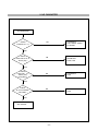
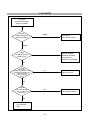
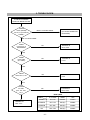
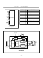
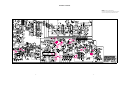
COLOR MONITOR
SERVICE MANUAL
CHASSIS NO. : CA-134
FACTORY MODEL: AS120J
MODEL: AS120-1, AS120-BK-1
CAUTION
BEFORE SERVICING THE UNIT,
READ THE SAFETY PRECAUTIONS IN THIS MANUAL.
CONTENTS
SPECIFICATIONS ................................................... 2
SAFETY PRECAUTIONS ........................................ 3
TIMING CHART ....................................................... 4
OPERATING INSTRUCTIONS ................................ 5
WIRING DIAGRAM ................................................. 6
BLOCK DIAGRAM ................................................... 7
DESCRIPTION OF BLOCK DIAGRAM................... ..8
ADJUSTMENT ...................................................... 10
TROUBLESHOOTING GUIDE .............................. 12
EXPLODED VIEW.................................................. 18
REPLACEMENT PARTS LIST .............................. 20
PIN CONFIGURATION .......................................... 26
SCHEMATIC DIAGRAM ......................................... 29
PRINTED CIRCUIT BOARD................................... 31
SPECIFICATIONS
1. PICTURE TUBE
Size
DefIection Angle
Neck Diameter
Mask Pitch
Diagonal Size
View Size
Face Treatment
3-2. Power Consumption
: 21 inch (Flat Slot Mask)
: 90°
: 29.1 mm
: 0.25 mm
: 508.0 mm
: 406.4 x 304.8 mm
: AR-ASC (Anti-Reflective and
Anti-Static Coating)
2. SIGNAL
2-1. Horizontal & Vertical Sync
1) Input Voltage Level : Low= ≤0.8V, High= ≥2.1V
2) Sync Polarity
: Positive or Negative
2-2. Video Input Signal
1) Voltage Level
a) Color 0, 0
b) Color 7, 0
c) Color 15, 0
2) Input Impedance
3) Video Color
4) Signal Format
MODE
POWER CONSUMPTION
LED COLOR
MAX
Yes
less than 110W
GREEN
STAND-BY
No
less than
8W
AMBER
SUSPEND
No
less than
8W
AMBER
DPM OFF
No
less than
3W
AMBER
4. DISPLAY AREA
4-1. Active Video Area :
• Max Image Size - 366.0 x 274.5mm (14.40" x 10.80")
• Preset Image Size - 350 x 262 mm (13.78" x 10.31")
4-2. Display Color
: Full Colors
4-3. Display Resolution : 1600 Dots x 1200Lines/75Hz
: 0 ~ 0.7 Vp-p
: 0 Vp-p
: 0.467 Vp-p
: 0.7 Vp-p
: 75 Ω
: R, G, B Analog
: Refer to the Timing Chart
2-3. Signal Connector
15 Pin D-Sub Connector
2-4. Scanning Frequency
Horizontal
: 31 ~ 96 kHz
Vertical
: 55 ~ 160 Hz
3. POWER SUPPLY
3-1. Power Range
AC 100~240V, 50/60HZ, 2A
4-4. Video Bandwidth
: 203MHz
5. ENVIRONMENT
5-1. Operating Temperature: 0°C ~ 40°C (32°F ~ 103°F)
(Ambient)
5-2. Relative Humidity
: 10% ~ 90%
(Non-condensing)
5-3. Altitude
: 10,000 ft
6. DIMENSIONS (with TILT/SWIVEL)
Width
: 498 mm (19.60")
Depth
: 512 mm (20.18")
Height
: 510 mm (20.07")
7. WEIGHT (with TILT/SWIVEL)
Net Weight
: 28 kg (61.74 lbs)
Gross Weight
: 32 kg (70.56 lbs)
-2-
SAFETY PRECAUTIONS
SAFETY-RELATED COMPONENT WARNING!
There are special components used in this color monitor
which are important for safety. These parts are marked
on the schematic diagram and the replacement
parts list. It is essential that these critical parts should be
replaced with the manufacturer's specified parts to
prevent X-radiation, shock, fire, or other hazards. Do not
modify the original design without obtaining written
permission from manufacturer or you will void the original
parts and labor guarantee.
CAUTION:
No modification of any circuit should be
attempted.
Service work should be performed only after
you are thoroughly familiar with all of the
following safety checks and servicing
guidelines.
SAFETY CHECK
Care should be taken while servicing this color monitor
because of the high voltage used in the deflection circuits.
These voltages are exposed in such areas as the
associated flyback and yoke circuits.
FIRE & SHOCK HAZARD
An isolation transformer must be inserted between the
color monitor and AC power line before servicing the
chassis.
• In servicing, attention must be paid to the original lead
dress specially in the high voltage circuit. If a short
circuit is found, replace all parts which have been
overheated as a result of the short circuit.
• All the protective devices must be reinstalled per the
original design.
• Soldering must be inspected for the cold solder joints,
frayed leads, damaged insulation, solder splashes, or
the sharp points. Be sure to remove all foreign
materials.
X-RADIATION
The only potential source of X-radiation is the picture tube.
However, when the high voltage circuit is operating
properly there is no possibility of an X-radiation problem.
The basic precaution which must be exercised is keep the
high voltage at the factory recommended level; the normal
high voltage is about 27.5kV. The following steps describe
how to measure the high voltage and how to prevent Xradiation.
Note : It is important to use an accurate high voltage
meter calibrated periodically.
• To measure the high voltage, use a high impedance
high voltage meter, connect (–) to chassis and (+) to
the CDT anode cap.
• Set the brightness control to maximum point at full
white pattern.
• Measure the high voltage. The high voltage meter
should be indicated at the factory recommended level.
• If the meter indication exceeds the maximum level,
immediate service is required to prevent the possibility
of premature component failure.
• To prevent X-radiation possibility, it is essential to use
the specified picture tube.
IMPLOSION PROTECTION
All used display tubes are equipped with an integral
implosion protection system, but care should be taken to
avoid damage and scratching during installation. Use only
same type display tubes.
-3-
CAUTION:
Please use only a plastic screwdriver to protect yourself
from shock hazard during service operation.
TIMING CHART
VIDEO
C
D
E
SYNC
B
F
A
MODE
H
O
MARK
Sync Polarity
Z
O
A
L
T
A
L
MODE 6
MODE 7
MODE 8
—
—
—
+
+
+
+
+
31.469
31.469
43.269
60.023
68.677
79.976
91.146
93.750
E
31.778
31.778
23.111
16.660
14.561
12.504
10.971
10.667
Video Active Time
µs
A
25.422
25.422
17.778
13.003
10.836
9.481
8.127
7.901
Blanking Time
µs
B
6.356
6.356
5.334
3.657
3.725
3.022
2.844
2.765
Front Porch
µs
C
0.640
0.640
1.556
0.203
0.508
0.119
0.406
0.316
Sync Duration
µs
D
3.810
3.810
1.556
1.219
1.016
1.067
1.016
0.948
Back Porch
µs
F
1.906
1.906
2.222
2.235
2.201
1.837
1.422
1.501
+
—
—
+
+
+
+
+
70.082
59.940
85.008
75.029
84.997
75.025
85.024
75.000
Frequency
Hz
Total Period
ms
E
14.270
16.683
11.763
13.328
11.765
13.329
11.761
13.333
Video Active Time
ms
A
12.700
15.253
11.093
12.795
11.183
12.804
11.235
12.800
Blanking Time
ms
B
1.557
1.430
0.670
0.533
0.582
0.525
0.527
0.533
Front Porch
ms
C
0.413
0.318
0.023
0.017
0.015
0.013
0.011
0.011
Sync Duration
ms
D
0.064
0.064
0.069
0.050
0.044
0.038
0.033
0.032
Back Porch
ms
F
1.08
1.049
0.578
0.466
0.523
0.475
0.483
0.490
Resolution
720
x
400
70Hz
640
x
480
60Hz
640
x
480
85Hz
1024
x
768
75Hz
1024
x
768
85Hz
1280
x
1024
75Hz
1280
x
1024
85Hz
1600
x
1200
75Hz
Recall
Yes
Yes
Yes
Yes
Yes
Yes
Yes
Yes
I
C
MODE 5
Total Period
Sync Polarity
R
MODE 4
µs
V
E
MODE 3
Frequency
N
T
MODE 2
kHz
R
I
MODE 1
-4-
WIRING DIAGRAM
P503
P401
P451
P402
P452 P453
FBT
P801
S+
SP901
P701
AC
Socket
Signal
Cable
P302
P301
P303
-6-
SIGNAL
INPUT
BLOCK DIAGRAM
-7-
DESCRIPTION OF BLOCK DIAGRAM
1. Line Filter & Associated Circuit.
5. X-ray Protection.
This is used for suppressing noise of power input line
flowing into the monitor and/or some noise generated
in this monitor flowing out through the power input
line.
That is to say, this circuit prevents interference
between the monitor and other electric appliances.
2. Degauss Circuit & Coil.
This circuit detects the rectified DC voltage comes
from the FBT pin 4. If the high voltage of the FBT
reaches up to about 30kV (abnormal state), H.V
control (IC802) detects. It stops B+ voltage supplied to
the FBT (T701), and high voltage is not be generated,
(In the normal state, the high voltage is about 27.5kV.)
6. Micom(Microprocessor) Circuit.
The degauss circuit consists of the degaussing coil,
the PTC (Positive Temperature Coefficient) thermistor
(TH901), and the relay (RL901). This circuit eliminates
abnormal color of the screen automatically by
degaussing the slot mask in the CDT when turn on the
power switch.
When you need to degauss while using the monitor,
select DEGAUSS on the OSD menu.
3. SMPS (Switching Mode Power Supply).
The operating procedure of Micom (Microprocessor)
and its associated circuit is as follows:
1) H and V sync signal is supplied from Signal Cable to the
Micom (IC401).
2) The Micom (IC401) distinguishes polarity and
frequency of H and V sync.
3) The Micom controls each OSD function signals.
(H-size, H-position, V-size, etc.)
4) The controlled data of each mode is stored in IC402.
User can adjust screen condition by each OSD
function. The data of the adjust screen condition is
stored automatically.
This circuit works with power of 100~240V
The operation procedure is as follows:
1) AC input voltage is rectified and smoothed by
the bridge diode (D901) and the capacitor (C905).
7. Horizontal and Vertical Synchronous Processor.
2) The rectified voltage (DC voltage) is applied to the
primary coil of the transformer (T901).
This circuit generates the horizontal drive pulse and
the vertical drive pulse by taking sync-signal from
Signal Cable. This circuit consists of the
TDA4841(IC801) and the associated circuit.
3) The control IC (IC901) generates switching pulse
to turn on and off the primary coil of the
transformer (T901) repeatedly.
4) Depending on the turn ratio of the transformer, the
secondary voltages appear at the secondary coil of
the transformer (T901).
5) These secondary voltages are rectified by each
diode (D924, D926, D923, D929, D922, D921,
D920) and operate the other circuits. (Deflection,
Video Amplifier, etc.)
8. Oscillating Circuit for D/D Converter.
This circuit generates the pulse wave which has the
horizontal period by taking the output of the
TDA4841(IC801).
9. D/D (DC to DC) Converter.
This circuit supplies DC voltage to the horizontal
deflection output circuit by decreasing DC 190V which
is the secondary voltage of the SMPS in accordance
with the input horizontal sync signal.
4. Display Power Management Circuit.
This circuit control power consumption of the monitor
by detecting H and V sync signal. There are stand-by
and suspend mode. When no horizontal or vertical
sync signal input, the circuit consists of Q913, Q915
and IC401 control signal becomes stand-by and
suspend mode. It’s power consumption is below 8W.
When no horizontal and vertical sync signal input, it’s
power consumption is below 3W.
10. D/D Drive & Convert Circuit.
This circuit is used for supplying B + voltage to
horizontal deflection output transistor (Q801).
11. Horizontal Deflection Output Circuit.
-8-
This circuit makes the horizontal deflection by
supplying the saw-tooth current to the horizontal
deflection yoke.
12. High Voltage Output & FBT (Flyback Transformer).
18. Static Convergence Control Circuit.
The high voltage output circuit is used for generating
pulse wave to the primary coil of the FBT (Flyback
Transformer (T701)). A boosted voltage (about
27.5kV) appears at the secondary of the FBT and it is
supplied to the anode of the CDT.
And there are another output voltages such as the
dynamic focus voltage.
This circuit corrects the convergence of the screen by
supplying the convergence signal to the H/V-STC coil
which is attached to the CDT near the deflection.
19. Moire Reduction Circuit
This circuit reduce interference between the periodical
display pattern and the CDT's slot (or dot).
The positions of every other one dot video signal
beams (red, green, and blue beam) are shifted finely,
thus reducing interference.
13. H-Linearity Correction Circuit.
This circuit corrects the horizontal linearity for each
horizontal sync frequency.
20. OSD Circuit.
14. Vertical Output Circuit.
This circuit is used for performing the OSD (OnScreen- Display) function.
When a user selects the OSD Select/Adjustment
control, the adjustment status displays on the screen.
This circuit takes the vertical wave from the
TDA4841(IC801) and performs the vertical deflection
by supplying the saw-tooth wave current from the
TDA4867J (IC601) to the vertical deflection yoke.
21. Video Pre-Amp Circuit.
15. Dynamic Focus Output Circuit.
This circuit amplifies the analog video signal from 00.7V to 0-4V. This circuit is operated by taking the
clamp, R, G, B drives, and contrast signals from the
Micom (IC401).
This circuit takes H and V parabola wave from the
TDA4841(IC801), and amplifies these waves to offer
to the FBT (T701).
16. H & V Blanking and Brightness Control.
22. Video Output Amp Circuit.
This circuit eliminates the retrace line by supplying a
negative pulse to the G1 of the CDT.
17. Image Rotation (Tilt) Circuit.
This circuit corrects the tilt of the screen by supplying
the image rotation signal to the tilt coil which is
attached to the CDT near the deflection.
-9-
This circuit amplifies the video signal which comes
from the video pre-amp circuit and amplified video
signal is applied to the CDT cathode.
ADJUSTMENT
GENERAL INFORMATION
3) EEPROM → ALL CLEAR → Y(Yes) command.
<Caution> Do not run this procedure unless the
EEPROM is changed. All data in EEPROM (mode
data and color data) will be erased.
4) COMMAND → PRESET START → Y(Yes)
command.
5) DIST. ADJ. → FOS. ADJ command.
6) Adjust H-POSITION as arrow keys to center of the
screen.
7) Adjust H-SIZE as arrow keys to 390 ± 2mm.
8) Adjust V-POSITION as arrow keys to center of the
screen.
9) Adjust V-SIZE as arrow keys to 293 ± 1mm.
10) Adjust TRAPEZOID as arrow keys to be the best
condition.
11) Adjust SIDE PINCUSHON as arrow keys to be the
best condition.
12) Adjust TILT as arrow keys to be the best condition.
13) Display cross hatch pattern at Mode 7.
14) DIST. ADJ. → BALANCE DATA command.
15) Adjust balance of Pin-Balance as arrow keys to be
the best condition.
16) Adjust parallelogram as arrow keys to be the best
condition.
17) Save of the Mode.
18) Save of the System.
19) Display from Mode 7 and repeat above from
number 6) to 16).
20) COMMAND → PRESET EXIT → Y (Yes) command.
All adjustment are thoroughly checked and corrected
when the monitor leaves the factory, but sometimes
several adjustments may be required.
Adjustment should be following procedure and after
warming up for a minimum of 30 minutes.
• Alignment appliances and tools.
- IBM compatible PC.
- Programmable Signal Generator.
(eg. VG-819 made by Astrodesign Co.)
- EPROM or EEPROM with saved each mode data.
- Alignment Adaptor and Software.
- Digital Voltmeter.
- White Balance Meter.
- Luminance Meter.
- High-voltage Meter.
AUTOMATIC AND MANUAL DEGAUSSING
The degaussing coil is mounted around the CDT so that
automatic degaussing when turn on the monitor. But a
monitor is moved or faced in a different direction, become
poor color purity cause of CDT magnetized, then press
DEGAUSSING on the OSD menu.
ADJUSTMENT PROCEDURE & METHOD
- Install the cable for adjustment such as Figure 1and run
the alignment program on the DOS for IBM compatible PC.
- Set external Brightness and Contrast volume to max position.
5. Adjustment for White Balance and Luminance.
1. Adjustment for B+ Voltage.
1) Display cross hatch pattern at Mode 7.
2) Adjust C905 (+) voltage to 190V ± 0.5V with VR901.
2. Adjustment for High-Voltage.
1) Display cross hatch pattern at Mode 7.
2) Adjust CDT Anode voltage to 27.5kV ± 0.2kV with
VR801.
3. Adjustment for Horizontal Raster Center.
1) Display cross hatch pattern at Mode 7.
2) Adjust the Back Raster should be center of the
screen with SW801.
4. Adjustment for Factory Mode (Preset Mode).
1) Display cross hatch pattern at Mode All.
2) Run alignment program for AS120J on the IBM
compatible PC.
- 10 -
1) Set the White Balance Meter.
2) Press the DEGAUSSING on the OSD menu for
demagnetization of the CDT.
3) Display color 0,0 pattern at Mode 7.
4) COMMAND → PRESET START → Y(Yes)
command.
5) Set Bightness and Contrast to max position.
6) COLOR ADJ. → LUMINANCE command of the
alignment program.
7) COLOR ADJ. → BIAS ADJ. command of the
alignment program.
8) Check whether blue color or not at R-BIAS and GBIAS to min position, Sub-Brightness to 100
position, B-BIAS to 90 position. If it's not blue color,
the monitor must repair.
9) Adjust Screen control on the FBT to 0.15 ± 0.02FL
of the raster luminance.
10) Adjust R-BIAS and G-BIAS command to x=0.283 ±
0.006 and y=0.298 ± 0.006 on the White Balance
Meter with PC arrow keys.
11) Display color 15,0 Full White(70x70mm) at mode 7.
12) DRIVE ADJ command.
13) Set B-DRIVE to 90(5A(h)) at DRIVE of the
alignment program.
14) Adjust R-DRIVE and G-DRIVE command to white
balance x=0.283 ± 0.003 and y=0.298 ± 0.003 on
the White Balance Meter with PC arrow keys.
15) Adjust SUB-CONTRAST command to 36±1FL of
the raster luminance.
15) Display color 15,0 full white patten at Mode 7.
16) COLOR ADJ. → LUMINANCE → ABL command.
17) Adjust ABL to 26 ± 1FL of the luminance.
18) Exit from the program.
- 11 -
6. Adjustment for Focus.
1) Display H character in full screen at Mode 7.
2) Adjust two Focus control on the FBT that focus
should be the best condition.
TROUBLESHOOTING GUIDE
1. NO POWER
NO POWER
(POWER INDICATOR OFF)
CHECK
FUSE OK?
(F901)
NO
TROUBLE IN
FUSE (F901)
NO
TROUBLE IN
BRIDGE DIODE
(D901)
YES
CHECK
D901
BRIDGE DIODE?
YES
CHECK
C905(+) VOLTAGE
145VDC at 110V input
310VDC at 220V input
NO
TROUBLE IN
IC901
YES
CHECK
D924, D926, D923,
D922, D921, D920 ?
NO
YES
TROUBLE IN
Q912, Q913, Q915, Q914,
IC903, IC904, Q902
- 12 -
TROUBLE IN
D924, D926, D923,
D922, D921, D920
2. NO CHARACTER
NO CHARACTER
CHECK
IC302 PIN 5, 6, 7 ?
NO
TROUBLE IN
P301, SIGNAL CABLE,
PC SIGNAL
YES
CHECK
IC302 PIN 19, 20, 21
PIN 10 (5V) ?
NO
TROUBLE IN
IC302, P302
NO
TROUBLE IN
IC303
NO
TROUBLE IN
IC304
YES
CHECK
IC303 PIN 1, 3, 5
PIN10 (12V),
PIN 6 (80V) ?
YES
CHECK
R, G, B CATHODE
VOLTAGE?
YES
TROUBLE IN
CDT SOCKET
- 13 -
3. NO RASTER
NO VIDEO
(POWER INDICATOR
GREEN or AMBER)
CHECK
POWER INDICATOR
GREEN or AMBER ?
AMBER
TROUBLE IN
P302 SIGNAL CABLE
GREEN
CHECK
SCREEN CONTROL
KNOB OF FBT
ROTATE SCREEN
CONTROL KNOB TO
CLOCKWISE or
COUNTER CLOCKWIES
OK
CHECK
VOLTAGE AT
D924/D926 CATHODE (190V)
D923/D929 CATHODE (80V)
IC904 OUT (12V)
D921 CATHODE
(6.3V)?
NO
TROUBLE IN PRIMARY
CIRCUIT OF T901
NO
TROUBLE IN
CDT SOCKET, BOARD
YES
CHECK
IC401 (MICOM) PIN 6
5V (HIGH), IC801 PIN 10
12V (HIGH)?
YES
TROUBLE IN
IC401 (MICOM),
IC801
- 14 -
4. NO VERTICAL DEFLECTION
NO V-DEFLECTION
(ONE HORIZONTAL LINE)
CHECK
IC601 Pin 3
(15V) ?
NO
TROUBLE IN
T901 15V LINE
NO
TROUBLE IN
T701 47V LINE
NO
TROUBLE IN
IC801
YES
CHECK
IC601 PIN 7
(47V)?
YES
CHECK
IC801 PIN 12
(SAWTOOTH WAVE)?
YES
TROUBLE IN
IC601, V-CIRCUIT
- 15 -
5. TROUBLE IN DPM
STAND-BY/SUSPEND/
DPMS OFF MODE FAILURE
CHECK
IC401 (MICOM)
PIN 40, 41 (H/V INPUT)
SIGNAL?
CHECK PC,
(PC IS NOT GOING INTO
DPM MODE)
INPUT H/V SYNC SIGNAL
NO H/V SYNC SIGNAL
CHECK
IC401 PIN 9, 8
WAVEFORM?
NO
TROUBLE IN
X401, IC401
NO
TROUBLE IN
IC401
NO
TROUBLE IN
IC401
YES
CHECK
IC401 PIN 6
(5V, HIGH)?
YES
CHECK
IC401 PIN 17, 18 ?
YES
CHECK
B+ LINE
(12V, 15V, 80V,
5V) ?
TROUBLE IN
Q913, Q915
NO
DPMS TABLE
TROUBLE IN
T901 or PC
Item
H / V SYNC
VIDEO
LED
NORMAL
ON / ON
NORMAL
GREEN
STAND-BY
OFF / ON
OFF(0V)
AMBER
SUSPEND
ON / OFF
OFF(0V)
AMBER
OFF
OFF / OFF
OFF(0V)
AMBER
Mode
- 16 -
6. NO DEGAUSSING
NO DEGAUSSING
CHECK
IC401 PIN 6
(5V)?
NO
TROUBLE IN
IC401 (MICOM)
NO
TROUBLE IN
D925
NO
TROUBLE IN
P901
NO
TROUBLE IN
RL901
YES
CHECK
Q920 COLLECTOR
VOLTAGE
(0.5V)?
YES
CHECK
P901?
YES
CHECK
RL901?
YES
TROUBLE IN
TH901,
DEGAUSSING COIL
- 17 -
OPERATING INSTRUCTIONS
FRONT VIEW
REAR VIEW
D-Sub Signal Connector
Front Control Panel
Power ON/OFF Button
AC Power Socket
Power Indicator
Front Control Panel
5
4
1. Power ON/OFF Button
This button is used to turn the monitor ON and OFF.
3
2
1
3. + / – Adjust Buttons
Use these buttons for adjusting the level of the
selected item.
2. Power Indicator
This indicator lights up green when the monitor
operates normally; in DPMS (Energy Saving) mode, DPM off mode - it color changes to orange.
4. SELECT Button
Use these button for selecting an OSD icon to be
adjusted.
5. OSD Select Buttons
Use these buttons to choose items in the on screen
display.
-5-
- 18 -
2
1
5
A
5
6
5
15
B
5
7
8
9
14
14
10
14
16
EXPLODED VIEW
14
14
13
14
11
12
3
4
17
EXPLODED VIEW PARTS LIST
Ref. No.
Part No.
Description
3091TKD003G
CABINET ASSEMBLY, CN291E NEC D003 AF345 - White
3091TKD003H
CABINET ASSEMBLY, CN291E NEC D003 AS120 - Black
6318G21001A
CDT(CIRC), M51QBN291X115(E-TCO) SAMSUNG 107KHZ 29.1MM FST
3809TKD001K
BACK COVER ASSY, CN291E(NEC) D001 8A793 - White
1
2
3
3809TKD001M BACK COVER ASSEMBLY, CN291E D001E E-CORE AS120 - Black
3043TKK002L
TILT SWIVEL ASSY, CN291B(NEC) B002,T002 8A793 - White
3043TKK002M
TILT SWIVEL ASSEMBLY, AS120J TKB002A/TKT002A AF-320T STEALTH BLACK
4
5
339-002K
6
4951TKS010L
METAL ASSY, FRAME CN291E(NEC)
7
6140TC4001J
COIL,DEGAUSSING, LX31 GET 1410MM,0.55*120TS,12.5 OHM,W/O PURITY
8
6174T13010M
FBT (FLY BACK TRANSFORMER), FQM19A015,UL TUBE,AS120J SAMSUNG 19”
9
6200TJB001N
FILTER(CIRC),EMC, 02MD5 DELTA BK F900BJ
10
4950TKK339A
METAL, REAR BRACKET(CN291E)
11
4810TKM040E
BRACKET, AS120J MAIN PC+ABS [“B”-”B” CORE]
12
4950TKS087A
METAL, FRAME (CB221)
13
4950TKS088A
METAL, FRAME BOTTOM(CB221)
14
1SZZTER001A SCREW,DRAWING, D3.0 L6.0 MSWR/FZMY DOUBLE
15
6871TST438A
PWB(PCB) ASSEMBLY,SUB, AS120J CONTROL TOTAL NEC CA-134
16
4815TKK004F
SHIELD ASSEMBLY, TOP AS120J
17
332-102H
A
6871TMT469A
PWB(PCB) ASSEMBLY,MAIN, AS120J ASRDM NEC CA-134 TOTAL
B
3313T21010A
MAIN TOTAL ASSEMBLY, AS120J NEC CA-134
SCREW ASSEMBLY, TAPTITE P TYPE D5.0 L25.0 MSWR/FZMY .
SCREW,, PTP 4*40 (FZMW)
- 19 -
REPLACEMENT PARTS LIST
CAUTION: BEFORE REPLACING ANY OF THESE COMPONENTS,
READ CAREFULLY THE SAFETY PRECAUTIONS IN THIS MANUAL.
* NOTE : S SAFETY Mark
AL ALTERNATIVE PARTS
*S *AL LOC. NO.
PART NO.
DATE: 2003. 8. 25.
DESCRIPTION / SPECIFICATION
*S *AL LOC. NO.
MAIN BOARD
CAPACITORS
C101
C102
C301
C303
C304
C306
C307
C308
C309
C310
C311
C312
C313
C315
C317
C318
C319
C320
C321
C323
C324
C325
C328
C330
C331
C332
C333
C334
C335
C336
C339
C340
C341
C342
C344
C346
C347
C355
C372
C401
C402
C403
C404
C405
C406
C407
C410
C417
C452
C453
C454
C455
0CE106CF638
0CN1040K949
0CK1020K515
0CK3320K515
181-288B
181-288N
0CK1030K945
0CK1040K945
0CK1040K945
181-288E
181-288B
181-288B
181-288B
0CE476EF638
0CK1040K945
0CN1040K949
0CK1040K945
0CE107EN630
0CK1040K945
0CE107EH638
0CN1040K949
181-288E
0CE476CN618
181-288B
181-288E
181-288E
181-288E
181-288B
181-288B
0CC47001505
0CK2710W515
181-288B
0CK10302945
0CC2200W415
181-288C
0CK10302940
0CK10302940
0CE476CF638
0CN1040K949
0CC5600K415
0CE476CH638
0CK2710K515
0CK2710K515
0CK2710K515
0CC0400K115
0CC0400K115
0CK1040K945
0CK1040K945
0CE106CK638
0CE106CK638
0CN1040K949
0CN1040K949
C456
C457
C458
C459
C460
C601
C602
C603
C605
C611
C701
C702
C704
C705
C707
C708
C709
C710
C711
C712
C713
C730
C731
C732
C734
C735
C736
C738
C739
C740
C741
C742
C743
C744
C771
C772
C801
C802
C803
C804
C805
C806
C807
C808
C809
C810
C811
C812
C813
C814
C815
C817
C818
C819
“10UF SHL,SD 16V M FM5 TP 5”
0.1M 50V Z F TA52
1000PF 50V K B TR
3300P 50V K B TS
MKT 100V 104JTR PHS26104
MKT 100V 103JTR PHS86103
0.01UF 50V Z F TR
0.1UF 50V Z F TR
0.1UF 50V Z F TR
MKT 100V 474JTR PHS 26474
MKT 100V 104JTR PHS26104
MKT 100V 104JTR PHS26104
MKT 100V 104JTR PHS26104
47UF KMG 16V M FM5 TP 5
0.1UF 50V Z F TR
0.1M 50V Z F TA52
0.1UF 50V Z F TR
100UF KMG 100V M FM5 BULK
0.1UF 50V Z F TR
100UF KMG 25V M FM5 TP 5
0.1M 50V Z F TA52
MKT 100V 474JTR PHS 26474
47UF SHL 100V M FL TP5
MKT 100V 104JTR PHS26104
MKT 100V 474JTR PHS 26474
MKT 100V 474JTR PHS 26474
MKT 100V 474JTR PHS 26474
MKT 100V 104JTR PHS26104
MKT 100V 104JTR PHS26104
47PF 1KV K SL TR
270P 500V K B TS
MKT 100V 104JTR PHS26104
0.01UF 2KV Z F TR
22PF 500V J NP0 TR
MKT 100V 224JTR PHS 26224
0.01M 2KV Z F S
0.01M 2KV Z F S
“47UF SHL,SD 16V M FM5 TP 5”
0.1M 50V Z F TA52
56P 50V J NP0 TP
“47UF SHL,SD 25V M FM5 TP 5”
270P 50V K B TS
270P 50V K B TS
270P 50V K B TS
4P
50V D NP0 TS
4P
50V D NP0 TS
0.1UF 50V Z F TR
0.1UF 50V Z F TR
“10UF SHL,SD 50V M FM5 TP 5”
“10UF SHL,SD 50V M FM5 TP 5”
0.1M 50V Z F TA52
0.1M 50V Z F TA52
- 20 -
PART NO.
0CN1040K949
181-288E
0CK1040K945
0CK1010K515
0CE475CK638
0CQ6821N419
181-288G
0CK1020W515
0CE476CN618
0CE108CH618
0CE106CK638
0CE337EN630
0CBZTBU003M
0CE107CN618
0CE106CK638
0CE476CQ618
181-477A
0CC3300K405
0CQ4721N419
0CK2220K515
0CE107CH638
0CE476CH638
0CE105CK638
0CK1040K945
181-288T
0CK10302945
0CK10302945
0CE685CN638
0CK1040K945
0CE106EK638
0CC1000W105
0CC1000W105
0CE106CN638
0CN1020K519
0CK6810K515
0CK4710W515
0CQ6821N419
181-288B
0CE106CK638
181-288D
181-476R
0CE227CH638
181-288B
0CC1000K115
0CK1020K515
0CE105CK638
0CE476CH638
0CE107CH638
0CE106CK638
0CK5610K515
0CE227CF638
0CE476CH638
181-288J
181-477U
DATE: 2003. 8. 25.
DESCRIPTION / SPECIFICATION
0.1M 50V Z F TA52
MKT 100V 474JTR PHS 26474
0.1UF 50V Z F TR
100PF 50V K B TR
“4.7UF SHL,SD 50V M FM5 TP 5”
6800PF 100V J PE NI TP
MKT 100V 334JTR PHS26334
1000P 500V K B TS
47UF SHL 100V M FL TP5
1000UF SHL 25V M FL TP5
“10UF SHL,SD 50V M FM5 TP 5”
330UF KMG 100V M FM5 BULK
562J 20.0*14.0*8.5*10.0 800V
100UF SHL 100V M FL TP5
“10UF SHL,SD 50V M FM5 TP 5”
47U SHL 200V M FL TP5
102J 19.5*12.0*7.0*7.5 250V
33P 50V J SL TP
0.0047U 100V J POLY NI TP5
2200P 50V K B TS
“100UF SHL,SD 25V M FM5 TP 5”
“47UF SHL,SD 25V M FM5 TP 5”
“1UF SHL,SD 50V 20% FM5 TP 5”
0.1UF 50V Z F TR
MKT 100V 223KTR PHS85223
0.01UF 2KV Z F TR
0.01UF 2KV Z F TR
“6.8UF SHL,SD 100V 20% TP 5 F”
0.1UF 50V Z F TR
10UF KMG 50V M FM5 TP 5
10PF 500V D SL TR
10PF 500V D SL TR
“10UF SHL,SD 100V M FM5 TP 5”
1000P 50V K B TA52
680P 50V K B TS
470P 500V K B TS
6800PF 100V J PE NI TP
MKT 100V 104JTR PHS26104
“10UF SHL,SD 50V M FM5 TP 5”
MKT 100V 473JTR PHS26473
2200 D 100V H PP NI TP5
“220UF SHL,SD 25V M FM5 TP 5”
MKT 100V 104JTR PHS26104
10P 50V D NP0 TS
1000PF 50V K B TR
“1UF SHL,SD 50V 20% FM5 TP 5”
“47UF SHL,SD 25V M FM5 TP 5”
“100UF SHL,SD 25V M FM5 TP 5”
“10UF SHL,SD 50V M FM5 TP 5”
560P 50V K B TS
“220UF SHL,SD 16V M FM5 TP 5”
“47UF SHL,SD 25V M FM5 TP 5”
MKT 100V 563JTR PHS26563
333J 19.5*13.0*7.5*7.5 250V
*S *AL LOC. NO.
C820
C821
C823
C832
C833
C834
C835
C841
C842
C843
C844
C845
C846
C847
C848
C849
C850
C851
C852
C854
C855
C856
C857
C858
C859
C860
C861
C863
C864
C865
C891
C892
C893
C894
C895
C896
C902
C903
C904
C905
C906
C907
C908
C909
C910
C911
C912
C915
C916
C917
C918
C920
C921
C922
C923
C925
C926
C927
C928
C929
C930
C931
PART NO.
0CN1040K949
0CN1040K949
0CK1010K515
0CK10102515
181-482F
0CN1040K949
0CBZTTA001R
0CE476CR630
181-309H
0CQ3321N419
181-309H
181-288B
0CE108EF618
0CQ2221N419
0CK47101515
0CK6810W515
0CK1040K945
0CK1040K945
0CN1040K949
181-482J
181-482A
181-305J
181-305N
181-482C
181-482C
0CN1040K949
0CN1040K949
0CN1040K949
0CN1040K949
0CE105CK638
0CZZTFT001J
0CZZTFT001M
181-288B
0CZZTFT001L
181-288B
181-288Q
0CKZTTA003C
0CK10101515
181-304V
0CZZTAB001B
0CE475CN638
0CE336CK638
0CK1040K945
181-288T
0CZZTFT001N
0CE108CD618
0CE475CK638
0CE476CH638
0CK2220K515
0CKZTTA003C
0CKZTTA003C
0CC47001505
0CE227CR650
0CE337EN630
0CK1010W515
0CE228CH618
0CE108EF618
0CE228CH618
0CE108EF618
0CK1020K515
0CQ2721N419
0CK1010W515
DATE: 2003. 8. 25.
DESCRIPTION / SPECIFICATION
*S *AL LOC. NO.
0.1UF 50V Z F TR
0.1M 50V Z F TA52
100PF 50V K B TR
100PF D 2KV 10% B(Y5P) TR
274JF 18.0*17.0*10.0*7.5 250
0.1M 50V Z F TA52
103J 20.0*17.0*10.0*7.5 800V
“47UF SHL,SD 250V M FM5 BULK”
272J 23.0*17.0*10.0*15.0 1.6
3300P 100V J POLY NI TP
272J 23.0*17.0*10.0*15.0 1.6
MKT 100V 104JTR PHS26104
1000UF KMG 16V M FL TP 5
2200PF 100V J PE NI TP
470P 1KV K B TS
680P 500V K B TS
0.1UF 50V Z F TR
0.1UF 50V Z F TR
0.1M 50V Z F TA52
394J 18.0*19.0*12.0*7.5 250V
104J 18.0*13.0*7.0*7.5 250V
474J 26.0*17.0*10.5*15.0 250
105J 26.0*22.5*14.0*15.0 250
154J 18.0*14.0*8.0*7.5 250V
154J 18.0*14.0*8.0*7.5 250V
0.1M 50V Z F TA52
0.1M 50V Z F TA52
0.1M 50V Z F TA52
0.1M 50V Z F TA52
“1UF SHL,SD 50V 20% FM5 TP 5”
ECQB1H562JM3 562J 50V TP5.0
ECQB1H103JF3 MATSUSHITA 50V
MKT 100V 104JTR PHS26104
ECQB1H822JM3 822J 50V TP5.0
MKT 100V 104JTR PHS26104
MKT 100V 154JTR PHS26154
SC E 472M 14.0FF7 250V TP7.5
100PF 1KV K B TR
393J 19.5*15.5*9.5*10.0 400V
SMH/HC 470UF 400V 30*50 BK10
“4.7UF SHL,SD 100V M FM5 TP 5”
“33UF SHL,SD 50V M FM5 TP 5”
0.1UF 50V Z F TR
MKT 100V 223KTR PHS85223
ECQB1H123JM3 123J 50V TP5.0
1000UF SHL 10V M FL TP5
“4.7UF SHL,SD 50V M FM5 TP 5”
“47UF SHL,SD 25V M FM5 TP 5”
2200P 50V K B TS
SC E 472M 14.0FF7 250V TP7.5
SC E 472M 14.0FF7 250V TP7.5
47PF 1KV K SL TR
220UF SHL 250V M FM7.5 BULK
330UF KMG 100V M FM5 BULK
100P 500V K B TS
2200U SHL 25V M FL TP5
1000UF KMG 16V M FL TP 5
2200U SHL 25V M FL TP5
1000UF KMG 16V M FL TP 5
1000PF 50V K B TR
2700PF 100V J PE NI TP
100P 500V K B TS
C932
C953
C970
PART NO.
DATE: 2003. 8. 25.
DESCRIPTION / SPECIFICATION
0CC47001505
0CE477CF638
0CE476CH638
47PF 1KV K SL TR
470UF SHL TYPE 16V M FM5 TP
“47UF SHL,SD 25V M FM5 TP 5”
0DZ560009CE
0DZ560009CE
0DZ560009CE
0DL305029BA
0DZ560009CE
0DZ560009CE
0DS141489AB
0DS141489AB
0DS141489AB
0DS141489AB
0DS141489AB
0DS141489AB
0DS124409AA
0DS124409AA
0DS124409AA
0DS124409AA
0DS124409AA
0DS124409AA
0DS124409AA
0DS124409AA
0DS124409AA
0DR140059DA
0DS141489AB
0DS141489AB
0DS141489AB
0DS141489AB
0DS141489AB
0DS141489AB
0DS141489AB
0DR400409AC
0DR400409AC
0DS141489AB
0DR100009CA
0DS141489AB
0DR100009DA
0DRFJ00011A
0DS141489AB
0DS141489AB
0DD400709CB
0DD400709CB
0DD400709CB
0DS141489AB
0DS141489AB
0DS141489AB
0DS141489AB
0DS141489AB
0DS141489AB
0DS141489AB
0DS141489AB
0DS141489AB
0DS141489AB
0DS141489AB
0DS141489AB
0DS141489AB
0DS141489AB
0DS141489AB
MTZJ5.6B TP ROHM-K DO34 500
MTZJ5.6B TP ROHM-K DO34 500
MTZJ5.6B TP ROHM-K DO34 500
LTL-305DJ-0C2 TP LITEON GREE
MTZJ5.6B TP ROHM-K DO34 500
MTZJ5.6B TP ROHM-K DO34 500
1N4148 TP GRANDE DO-34 500MW
1N4148 TP GRANDE DO-34 500MW
1N4148 TP GRANDE DO-34 500MW
1N4148 TP GRANDE DO-34 500MW
1N4148 TP GRANDE DO-34 500MW
1N4148 TP GRANDE DO-34 500MW
1SS244 TP ROHM KOREA
1SS244 TP ROHM KOREA
1SS244 TP ROHM KOREA
1SS244 TP ROHM KOREA
1SS244 TP ROHM KOREA
1SS244 TP ROHM KOREA
1SS244 TP ROHM KOREA
1SS244 TP ROHM KOREA
1SS244 TP ROHM KOREA
1N4005TB52 TP LITEON DO41 60
1N4148 TP GRANDE DO-34 500MW
1N4148 TP GRANDE DO-34 500MW
1N4148 TP GRANDE DO-34 500MW
1N4148 TP GRANDE DO-34 500MW
1N4148 TP GRANDE DO-34 500MW
1N4148 TP GRANDE DO-34 500MW
1N4148 TP GRANDE DO-34 500MW
UF4004 GULF TP DO41 400V 1A
UF4004 GULF TP DO41 400V 1A
1N4148 TP GRANDE DO-34 500MW
RGP10G TP GULF SEMICONDUCTOR
1N4148 TP GRANDE DO-34 500MW
RGP10J TP GULF SEMICONDUCTOR
YG339D6F208 FUJI ST TO220 -4
1N4148 TP GRANDE DO-34 500MW
1N4148 TP GRANDE DO-34 500MW
UF4007 TP G.I DO204AL 1000V
UF4007 TP G.I DO204AL 1000V
UF4007 TP G.I DO204AL 1000V
1N4148 TP GRANDE DO-34 500MW
1N4148 TP GRANDE DO-34 500MW
1N4148 TP GRANDE DO-34 500MW
1N4148 TP GRANDE DO-34 500MW
1N4148 TP GRANDE DO-34 500MW
1N4148 TP GRANDE DO-34 500MW
1N4148 TP GRANDE DO-34 500MW
1N4148 TP GRANDE DO-34 500MW
1N4148 TP GRANDE DO-34 500MW
1N4148 TP GRANDE DO-34 500MW
1N4148 TP GRANDE DO-34 500MW
1N4148 TP GRANDE DO-34 500MW
1N4148 TP GRANDE DO-34 500MW
1N4148 TP GRANDE DO-34 500MW
1N4148 TP GRANDE DO-34 500MW
DIODEs
D101
D102
D103
D104
D105
D106
D301
D302
D303
D304
D305
D306
D307
D308
D309
D310
D311
D312
D313
D314
D315
D316
D401
D402
D405
D451
D452
D453
D454
D701
D702
D703
D704
D706
D707
D708
D709
D731
D732
D733
D734
D735
D736
D737
D738
D740
D771
D772
D773
D801
D802
D803
D804
D805
D808
D811
- 21 -
*S *AL LOC. NO.
PART NO.
DATE: 2003. 8. 25.
DESCRIPTION / SPECIFICATION
D812
D831
D832
D833
D834
D835
D836
D837
D838
D839
D840
D861
D901
D902
D903
D904
D905
D906
D907
D908
D909
D910
D911
D912
D913
D914
D920
D921
D922
D923
D924
D925
D926
D927
D928
D929
D951
ZD402
ZD403
ZD404
ZD405
ZD407
ZD408
ZD409
ZD410
ZD601
ZD703
ZD711
ZD712
ZD801
ZD802
ZD804
ZD901
ZD902
0DS141489AB
0DR260400AA
0DS141489AB
0DR140059DA
0DS141489AB
0DRGF00069A
0DRGF00069A
0DS141489AB
0DR200000EA
0DS141489AB
0DR100009DA
0DD140009AA
0DRGF00090A
0DRGF00109A
0DR100009CA
0DR100009DA
0DS141489AB
971-0054
0DS141489AB
0DS141489AB
0DS141489AB
0DRGF00139A
0DS141489AB
0DS141489AB
0DS141489AB
0DS141489AB
0DRSD00079A
0DRSD00079A
0DR540400AA
0DRGS00400A
0DR260400AA
0DS141489AB
0DR260400AA
0DS141489AB
971-0054
0DRGS00400A
0DR100009CA
0DZ560009AG
0DZ560009AG
0DZ560009AG
0DZ560009AG
0DZ560009AG
0DZ560009AG
0DZ560009AG
0DZ560009AG
0DZ560009AG
0DZ510009BE
0DZ180009BD
0DZ560009AG
0DZ110009AD
0DZ180009BD
0DZ180009BD
0DZ240009BJ
0DZ560009AG
1N4148 TP GRANDE DO-34 500MW
S2L60-4004P15 BK SHINDENGEN
1N4148 TP GRANDE DO-34 500MW
1N4005TB52 TP LITEON DO41 60
1N4148 TP GRANDE DO-34 500MW
SB140 GULF TP DO41 40V 1A 40
SB140 GULF TP DO41 40V 1A 40
1N4148 TP GRANDE DO-34 500MW
FMQ-G2FMS BK SANKEN NON 1500
1N4148 TP GRANDE DO-34 500MW
RGP10J TP GULF SEMICONDUCTOR
EK14 V(1) TP SANKEN E/EO-TMD
GBL06 GULF BK GBL 600V 4A 12
GUF10M GULF TP DO41 1000V 1A
RGP10G TP GULF SEMICONDUCTOR
RGP10J TP GULF SEMICONDUCTOR
1N4148 TP GRANDE DO-34 500MW
TIN 50MM TAPING
1N4148 TP GRANDE DO-34 500MW
1N4148 TP GRANDE DO-34 500MW
1N4148 TP GRANDE DO-34 500MW
GPP20J GULF TP DO15 600V 2.0
1N4148 TP GRANDE DO-34 500MW
1N4148 TP GRANDE DO-34 500MW
1N4148 TP GRANDE DO-34 500MW
1N4148 TP GRANDE DO-34 500MW
D2L20U SHINDENGEN TP DO-204A
D2L20U SHINDENGEN TP DO-204A
UF5404L BK G.I DO201AD 400V
31GF4 GENERAL SEMICONDUCTOR
S2L60-4004P15 BK SHINDENGEN
1N4148 TP GRANDE DO-34 500MW
S2L60-4004P15 BK SHINDENGEN
1N4148 TP GRANDE DO-34 500MW
TIN 50MM TAPING
31GF4 GENERAL SEMICONDUCTOR
RGP10G TP GULF SEMICONDUCTOR
GDZJ5.6B TP GRANDE DO-34 500
GDZJ5.6B TP GRANDE DO-34 500
GDZJ5.6B TP GRANDE DO-34 500
GDZJ5.6B TP GRANDE DO-34 500
GDZJ5.6B TP GRANDE DO-34 500
GDZJ5.6B TP GRANDE DO-34 500
GDZJ5.6B TP GRANDE DO-34 500
GDZJ5.6B TP GRANDE DO-34 500
GDZJ5.6B TP GRANDE DO-34 500
GDZ5.1B TP GRANDE DO34 500MW
GDZJ18B TP GRANDE DO34 0.5W
GDZJ5.6B TP GRANDE DO-34 500
MTZJ11B TP ROHM-K DO34 500MW
GDZJ18B TP GRANDE DO34 0.5W
GDZJ18B TP GRANDE DO34 0.5W
GDZJ24B TP GRANDE DO34 500MW
GDZJ5.6B TP GRANDE DO-34 500
IC302
IC303
IC304
IC401
IC402
0IPRPNS025A
0IPRPNS007A
0IPRPNS005A
0IZZTSZ241B
0ISG240860A
LM1246DDA/NA NATIONAL SEMICO
LM2463TA NATIONAL SEMICONDUC
LM2480NA NATIONAL SEMICONDUC
HBW96G6 WT62P1 42P ST MTP .
M24C08-BN6 8DIP BK 8K SERIAL
*S *AL LOC. NO.
IC601
IC702
IC801
IC802
IC901
IC903
IC904
PART NO.
0IPRPPH018A
0INS353000A
0IPRPPH005A
0IMI625010A
0ISS384300A
0ISS780500F
0IKE781200F
DATE: 2003. 8. 25.
DESCRIPTION / SPECIFICATION
“TDA4867J PHILIPS 9PIN,ST DIP”
LF353N OP-AMP
“TDA4841PS PHILIPS 32P,SDIP S”
M62501P 16P4 BK INTERFACE PW
KA3843B 8P SDIP BK PWM CONTR
KA7805
“KIA78L12BP(AT) 3P 12V,150MA”
COILs & COREs
FB301
FB302
FB303
FB304
FB305
FB306
FB309
FB310
FB311
FB401
FB402
FB403
FB404
FB405
FB406
FB407
FB701
FB801
FB841
FB901
FB902
FB903
FB904
FB905
FB906
FB907
FB908
FB909
L101
L301
L302
L303
L311
L312
L313
L701
L801
L805
L806
125-022J
125-155A
125-022J
125-022J
125-155J
125-155A
125-155B
125-155A
125-155A
125-155J
125-155N
125-155L
125-155F
125-155F
125-155J
125-155J
125-155J
125-155J
125-155P
125-155J
125-155A
125-155H
125-155H
125-155C
125-155H
125-155J
125-155J
0RX0331L665
125-155J
0LA0220K119
0LA0220K119
0LA0220K119
0LA0270K119
0LA0270K119
0LA0270K119
6140TBZ009D
6140TYZ009B
150-985P
150-985N
FERRITE KQ-1 JS 3.5*5.0MM AX
BFD3510R2FG SAMWHA 3.5*10MM
FERRITE KQ-1 JS 3.5*5.0MM AX
FERRITE KQ-1 JS 3.5*5.0MM AX
BFS2550A0FG SAMWHA 2.5*5.0MM
BFD3510R2FG SAMWHA 3.5*10MM
BFS3580R2FG SAMWHA 3.5*8.0MM
BFD3510R2FG SAMWHA 3.5*10MM
BFD3510R2FG SAMWHA 3.5*10MM
BFS2550A0FG SAMWHA 2.5*5.0MM
BFD3565R2FG SAMWHA 3.5*6.5MM
BFS3580A0FG SAMWHA 3.5*8.0MM
BFD3580R2FG SAMWHA 3.5*8.0MM
BFD3580R2FG SAMWHA 3.5*8.0MM
BFS2550A0FG SAMWHA 2.5*5.0MM
BFS2550A0FG SAMWHA 2.5*5.0MM
BFS2550A0FG SAMWHA 2.5*5.0MM
BFS2550A0FG SAMWHA 2.5*5.0MM
BFS2550R2FG SAMWHA 2.5*5.0MM
BFS2550A0FG SAMWHA 2.5*5.0MM
BFD3510R2FG SAMWHA 3.5*10MM
BFS3510A0FG SAMWHA 3.5*10MM
BFS3510A0FG SAMWHA 3.5*10MM
BFD3514R2FG SAMWHA 3.5*14MM
BFS3510A0FG SAMWHA 3.5*10MM
BFS2550A0FG SAMWHA 2.5*5.0MM
BFS2550A0FG SAMWHA 2.5*5.0MM
3.3 OHM 3 W 5% SF
BFS2550A0FG SAMWHA 2.5*5.0MM
0.22UH K 2.3*3.4 TP
0.22UH K 2.3*3.4 TP
0.22UH K 2.3*3.4 TP
0.27UH K 2.3*3.4 TP
0.27UH K 2.3*3.4 TP
0.27UH K 2.3*3.4 TP
“- GET NO CORE,0.1*30 50TS,10”
“DR 14*15-C5.2 14*9T 13.5T,1.”
DR12*15 6MH 0.25MM 365.5T
DR10*10 4.7UH 0.16MM 322.5
TRANSISTOR
Q301
Q302
Q451
Q452
Q453
Q454
Q455
Q456
Q458
Q459
ICs
- 22 -
0TR127509AC
0TR231609AA
0TR488009AA
0TR127009AA
0TR320209AA
0TR488009AA
0TR127009AA
0TR320209AA
0TR320509AB
0TR127309AA
KTA1275-Y(KTA1013) TP KEC TO
KSC2316-Y TP SAMSUNG TO92L
BF488 TP PHILIPS TO92 PNP
KTA1270-Y(KTA562TM) TP KEC T
KTC3202-Y(KTC1959) TP KEC TO
BF488 TP PHILIPS TO92 PNP
KTA1270-Y(KTA562TM) TP KEC T
KTC3202-Y(KTC1959) TP KEC TO
KTC3205-Y(KTC2236A) TP KEC T
KTA1273-Y(KTA966A) TP KEC TO
*S *AL LOC. NO.
Q701
Q704
Q705
Q706
Q707
Q708
Q721
Q723
Q724
Q725
Q726
Q771
Q801
Q802
Q803
Q804
Q806
Q807
Q808
Q810
Q811
Q812
Q832
Q833
Q834
Q836
Q837
Q838
Q839
Q841
Q842
Q843
Q844
Q901
Q902
Q903
Q912
Q913
Q914
Q915
Q920
PART NO.
0TR320509AB
0TFFN10003C
0TR320209AA
0TR127009AA
0TR390409CA
0TR319809AA
0TR390409CA
0TR390409CA
0TR463300AB
0TR463300AB
0TR555109AB
0TR920009AB
0TR558900BA
0TR471009AA
0TR564009AB
0TR319809AA
0TR471009AA
0TR564009AB
0TR127009AA
0TR114009AB
0TF630000CA
0TR114009AB
0TF283509AA
0TFFC10008A
0TR231609AA
0TF630000CA
0TF630000CA
0TF630000CA
0TF640000CA
0TR114009AB
0TR114009AB
0TR114009AB
0TR114009AB
0TFFN10003C
0DR100609BA
0TR319809AA
0TR127309AA
0TR319809AA
0TR928009AB
0TR319809AA
0TR319809AA
DATE: 2003. 8. 25.
DESCRIPTION / SPECIFICATION
*S *AL LOC. NO.
KTC3205-Y(KTC2236A) TP KEC T
INFINEON SPA07N60C3(E8153) S
KTC3202-Y(KTC1959) TP KEC TO
KTA1270-Y(KTA562TM) TP KEC T
FAIRCHILD 2N3904(TA) TP TO-9
KTC3198-Y(KTC1815) TP KEC TO
FAIRCHILD 2N3904(TA) TP TO-9
FAIRCHILD 2N3904(TA) TP TO-9
2SC4633(LS-CB11) BK SANYO L
2SC4633(LS-CB11) BK SANYO L
2N5551 TP SAMSUNG TO92 AMP
KSP92 TP SAMSUNG TO92 HIGH V
“2SC5589(LG,W/M) BK TOSHIBA T”
KSD471AC-Y TP SAMSUNG TO92
KSB564AC-YTA TP SANSUNG TO92
KTC3198-Y(KTC1815) TP KEC TO
KSD471AC-Y TP SAMSUNG TO92
KSB564AC-YTA TP SANSUNG TO92
KTA1270-Y(KTA562TM) TP KEC T
DTC114ES TP ROHM-K SPT NPN
IRFS630A BK SAMSUNG 200V 6.5
DTC114ES TP ROHM-K SPT NPN
2SK2835(TP) TP TOSHIBA 200V
SFS9634 FAIRCHILD ST TO220F
KSC2316-Y TP SAMSUNG TO92L
IRFS630A BK SAMSUNG 200V 6.5
IRFS630A BK SAMSUNG 200V 6.5
IRFS630A BK SAMSUNG 200V 6.5
IRFS640A BK SAMSUNG 200V 9A
DTC114ES TP ROHM-K SPT NPN
DTC114ES TP ROHM-K SPT NPN
DTC114ES TP ROHM-K SPT NPN
DTC114ES TP ROHM-K SPT NPN
INFINEON SPA07N60C3(E8153) S
MCR100-6RLRA TP MOTOROLA TO9
KTC3198-Y(KTC1815) TP KEC TO
KTA1273-Y(KTA966A) TP KEC TO
KTC3198-Y(KTC1815) TP KEC TO
KSA928A-Y TP SAMSUNG TO92L P
KTC3198-Y(KTC1815) TP KEC TO
KTC3198-Y(KTC1815) TP KEC TO
R315
R319
R320
R326
R327
R328
R329
R330
R331
R332
R333
R334
R335
R336
R337
R340
R341
R342
R343
R344
R345
R346
R347
R401
R402
R403
R405
R406
R407
R412
R413
R414
R415
R416
R418
R419
R420
R421
R422
R423
R424
R425
R426
R428
R429
R430
R431
R432
R434
R440
R443
R451
R452
R453
R454
R455
R456
R457
R458
R459
R460
R461
RESISTORs
R101
R102
R103
R104
R105
R106
R107
R108
R109
R110
R301
R302
R303
R305
R306
R307
R308
R314
0RD1800Q609
0RD2200Q609
0RD2200Q609
0RD3600Q609
0RD5600Q609
0RD2400Q609
0RD1001Q609
0RD1001Q609
0RD1800Q609
0RD1800Q609
0RD0752Q609
0RD0752Q609
0RD0752Q609
0RN6201F409
0RD1002Q609
0RD5102Q509
0RD1002Q609
0RD1000Q609
180 1/4W(3 5% TA52
220 1/4W(3 5% TA52
220 1/4W(3 5% TA52
360 1/4W(3 5% TA52
560 1/4W(3 5% TA52
240 OHM 1/4 W (3.4) 5% TA52
1K 1/4W(3 5% TA52
1K 1/4W(3 5% TA52
180 1/4W(3 5% TA52
180 1/4W(3 5% TA52
75 1/4W(3 5% TA52
75 1/4W(3 5% TA52
75 1/4W(3 5% TA52
6.20K 1/6W 1% TA52
10K 1/4W(3 5% TA52
51K OHM 1/4 W (3.4) 2% TA52
10K 1/4W(3 5% TA52
100 1/4W(3 5% TA52
- 23 -
PART NO.
0RD1000Q609
0RD8201Q609
0RD4701Q609
0RD4701Q609
0RD2001Q609
0RD2001Q609
0RD2001Q609
0RD1000Q609
0RD1600Q609
0RD1800Q609
0RD1300Q609
0RD3303Q609
0RD3303Q609
0RD3303Q609
0RD3000Q609
0RN1002F409
0RD0332A609
0RD0332A609
0RD0332A609
0RD0332Q609
0RD0332Q609
0RD0332Q609
971-0054
0RD3300Q609
0RD1000Q609
0RD4701Q609
0RD4701Q609
0RD4701Q609
0RD1000Q609
0RD1000Q609
0RD2202Q609
0RD2202Q609
0RD2202Q609
0RD2202Q609
0RD2000Q609
0RN1002F409
0RD4701Q609
0RD1001Q609
0RD4701Q609
0RD1000Q609
0RN2201F409
0RD2001Q609
0RD2001Q609
0RD1000Q609
0RD1000Q609
0RD1801Q609
0RD1801Q609
0RD1301Q609
0RN1002F409
0RD1000Q609
0RD1001Q609
0RD4701Q609
0RD4701Q609
0RD1500Q609
0RD6201Q609
0RD0272A609
0RD0272A609
0RD4701Q609
0RD4701Q609
0RD1500Q609
0RD6201Q609
0RX0472J609
DATE: 2003. 8. 25.
DESCRIPTION / SPECIFICATION
100 1/4W(3 5% TA52
8.20K 1/4W(3 5% TA52
4.70K 1/4W(3 5% TA52
4.70K 1/4W(3 5% TA52
2K 1/4W(3 5% TA52
2K 1/4W(3 5% TA52
2K 1/4W(3 5% TA52
100 1/4W(3 5% TA52
160 1/4W(3 5% TA52
180 1/4W(3 5% TA52
130 1/4W(3 5% TA52
330K 1/4W(3 5% TA52
330K 1/4W(3 5% TA52
330K 1/4W(3 5% TA52
300 1/4W(3 5% TA52
10K 1/6W 1 TA52
33 OHM 1/2 W (7.0) 5% TA52
33 OHM 1/2 W (7.0) 5% TA52
33 OHM 1/2 W (7.0) 5% TA52
33 1/4W(3 5% TA52
33 1/4W(3 5% TA52
33 1/4W(3 5% TA52
TIN 50MM TAPING
330 1/4W(3 5% TA52
100 1/4W(3 5% TA52
4.70K 1/4W(3 5% TA52
4.70K 1/4W(3 5% TA52
4.70K 1/4W(3 5% TA52
100 1/4W(3 5% TA52
100 1/4W(3 5% TA52
22K 1/4W(3 5% TA52
22K 1/4W(3 5% TA52
22K 1/4W(3 5% TA52
22K 1/4W(3 5% TA52
200 1/4W(3 5% TA52
10K 1/6W 1 TA52
4.70K 1/4W(3 5% TA52
1K 1/4W(3 5% TA52
4.70K 1/4W(3 5% TA52
100 1/4W(3 5% TA52
2.20K 1/6W 1% TA52
2K 1/4W(3 5% TA52
2K 1/4W(3 5% TA52
100 1/4W(3 5% TA52
100 1/4W(3 5% TA52
1.80K 1/4W(3 5% TA52
1.80K 1/4W(3 5% TA52
1.30K 1/4W(3 5% TA52
10K 1/6W 1 TA52
100 1/4W(3 5% TA52
1K 1/4W(3 5% TA52
4.70K 1/4W(3 5% TA52
4.70K 1/4W(3 5% TA52
150 1/4W(3 5% TA52
6.20K 1/4W(3 5% TA52
27 OHM 1/2 W (7.0) 5% TA52
27 OHM 1/2 W (7.0) 5% TA52
4.70K 1/4W(3 5% TA52
4.70K 1/4W(3 5% TA52
150 1/4W(3 5% TA52
6.20K 1/4W(3 5% TA52
47 OHM 1 W 5% TA52
*S *AL LOC. NO.
R462
R463
R464
R465
R466
R467
R473
R493
R494
R601
R602
R603
R604
R605
R606
R607
R608
R609
R610
R701
R702
R703
R704
R705
R706
R707
R710
R711
R712
R714
R715
R716
R717
R718
R718-1
R719
R720
R721
R722
R723
R729
R730
R731
R732
R733
R734
R735
R736
R737
R738
R739
R740
R741
R742
R743
R744
R745
R746
R747
R748
R749
R750
PART NO.
0RD0102A609
0RD6801Q609
0RN1000F409
0RN6202F409
0RD4302Q609
0RN5601F409
0RD1004Q609
0RD1000Q609
0RD1000Q609
0RD2001Q609
0RD2001Q609
0RD0111A509
0RD0331A609
0RN1302F409
0RN1302F409
0RD1200A609
0RD1000Q609
0RD1000A609
0RN0390H609
0RMZTWD001K
0RD1002Q609
0RD3301Q609
0RD2201Q609
0RB0150K609
0RD1003Q609
0RD5601Q609
0RD0472Q609
0RN1502F409
0RD1003Q609
0RD1001Q609
0RD5601Q609
0RD1004Q609
0RD1000Q609
0RN0101H609
0RN0111H509
0RD0332Q609
0RD4701Q609
0RN7501F409
0RD1003Q609
0RN1302F409
0RX0102J609
0RD6802Q609
0RD1000Q609
0RD1001Q609
0RD5602Q609
0RD2001Q609
0RD1002Q609
0RX2001J609
0RD6801Q609
0RN2702F409
0RC1004A609
0RN1503G409
0RD2001Q609
0RD6800Q609
0RD1000A609
0RX1502J609
0RD0472Q609
0RX1503L607
0RX1503L607
0RD0472Q609
0RD4300Q609
0RD6800Q609
DATE: 2003. 8. 25.
DESCRIPTION / SPECIFICATION
*S *AL LOC. NO.
10 OHM 1/2 W (7.0) 5% TA52
6.80K 1/4W(3 5% TA52
100OHM 1/6 W 1% TA52
62KOHM 1/6 W 1% TA52
43K 1/4W(3 5% TA52
5.60K 1/6W 1% TA52
1M OHM 1/4 W (3.4) 5% TA52
100 1/4W(3 5% TA52
100 1/4W(3 5% TA52
2K 1/4W(3 5% TA52
2K 1/4W(3 5% TA52
1.1 OHM 1/2 W(7.0) 2% TA52
3.3 OHM 1/2 W (7.0) 5% TA52
13K 1/6W 1% TA52
13K 1/6W 1% TA52
120 OHM 1/2 W (7.0) 5% TA52
100 1/4W(3 5% TA52
100 OHM 1/2 W (7.0) 5% TA52
0.39 1/2W 5 TA52
RWR SMART 100OHM 7 W 5% PD T
10K 1/4W(3 5% TA52
3.30K 1/4W(3 5% TA52
2.20K 1/4W(3 5% TA52
0.15 OHM 2 W 5% TA52
100K 1/4W(3 5% TA52
5.60K 1/4W(3 5% TA52
47 1/4W(3 5% TA52
15K 1/6W 1% TA52
100K 1/4W(3 5% TA52
1K 1/4W(3 5% TA52
5.60K 1/4W(3 5% TA52
1M OHM 1/4 W (3.4) 5% TA52
100 1/4W(3 5% TA52
1.0 1/2W 5 TA52
1.1 OHM 1/2 W 2.00% TA52
33 1/4W(3 5% TA52
4.70K 1/4W(3 5% TA52
7.50K 1/6W 1% TA52
100K 1/4W(3 5% TA52
13K 1/6W 1% TA52
10 OHM 1 W 5% TA52
68K 1/4W(3 5% TA52
100 1/4W(3 5% TA52
1K 1/4W(3 5% TA52
56K OHM 1/4 W(3.4) 5.00% TA5
2K 1/4W(3 5% TA52
10K 1/4W(3 5% TA52
2K OHM 1 W 5% TA52
6.80K 1/4W(3 5% TA52
27K 1/6W 1% TA52
1M OHM 1/2 W(7.0) 5% TA52
150K 1/4W 1 TA52
2K 1/4W(3 5% TA52
680 1/4W(3 5% TA52
100 OHM 1/2 W (7.0) 5% TA52
15KOHM 1 W 5% TA52
47 1/4W(3 5% TA52
150K OHM 3 W 5% TA62
150K OHM 3 W 5% TA62
47 1/4W(3 5% TA52
430 OHM 1/4 W(3.4) 5.00% TA5
680 1/4W(3 5% TA52
R764
R771
R773
R774
R775
R776
R780
R781
R801
R802
R803
R805
R806
R807
R808
R809
R810
R811
R812
R813
R814
R815
R816
R817
R818
R822
R823
R824
R825
R826
R827
R830
R831
R835
R836
R837
R838
R841
R842
R843
R846
R847
R848
R849
R850
R851
R853
R855
R857
R859
R860
R861
R862
R864
R865
R871
R872
R873
R874
R875
R876
R878
- 24 -
PART NO.
0RD0472Q609
0RD1101Q609
0RN6202H409
0RN4302G409
0RD3300Q609
0RD7502Q609
0RD2202Q609
0RX4300K607
0RD1502Q609
0RD2002Q509
0RD3302Q609
0RD1002Q609
0RD1002Q609
0RD1001Q609
0RD1001Q609
0RD3602F509
0RD1001Q609
0RD1001Q609
0RD2201Q609
0RD2401Q609
0RN1202F409
0RN4700F409
0RD1001Q609
0RD1002Q609
0RD2701Q609
0RN3601F409
0RD2703Q609
0RN4700F409
0RN1002F409
0RN1602F409
0RN1002F409
0RD1002Q609
0RN1002F409
0RD4700Q609
0RD1002A609
0RN1202F409
0RD0101Q609
0RD5601Q609
0RMZTWD001A
0RX1003J609
0RD0332A609
0RD1000A609
0RD0471A609
0RX1300J609
0RMZTWD001C
0RD4701Q609
0RD4701Q609
0RD4701Q609
0RD3001Q609
0RD0102Q609
0RD2000Q609
0RMZTWV001J
0RB0120K607
0RD2202Q609
0RD4701Q609
0RX1500K607
0RD2401Q609
0RD0122A609
0RX0332K607
0RX0242K607
0RN3002F409
0RX0182K607
DATE: 2003. 8. 25.
DESCRIPTION / SPECIFICATION
47 1/4W(3 5% TA52
1.1K OHM 1/4 W (3.4) 5% TA52
62000 OHM 1/2 W 1% TA52
43K OHM 1/4 W 1% TA52
330 1/4W(3 5% TA52
75K 1/4W(3 5% TA52
22K 1/4W(3 5% TA52
430 OHM 2 W 5% TA62
15K 1/4W(3 5% TA52
20K OHM 1/4 W (3.4) 2% TA52
33K 1/4W(3 5% TA52
10K 1/4W(3 5% TA52
10K 1/4W(3 5% TA52
1K 1/4W(3 5% TA52
1K 1/4W(3 5% TA52
36K 1/6W 2% TA52
1K 1/4W(3 5% TA52
1K 1/4W(3 5% TA52
2.20K 1/4W(3 5% TA52
2.40K 1/4W(3 5% TA52
12K 1/6W 1% TA52
470 1/6W 1 TA52
1K 1/4W(3 5% TA52
10K 1/4W(3 5% TA52
2.70K 1/4W(3 5% TA52
3.6K 1/6W 1 TA52
270K 1/4W(3 5% TA52
470 1/6W 1 TA52
10K 1/6W 1 TA52
16K 1/6W 1% TA52
10K 1/6W 1 TA52
10K 1/4W(3 5% TA52
10K 1/6W 1 TA52
470 OHM 1/4 W (3.4) 5% TA52
10K OHM 1/2 W (7.0) 5% TA52
12K 1/6W 1% TA52
1 1/4W(3 5% TA52
5.60K 1/4W(3 5% TA52
4.7 OHM 5 W 5% B RWR
100KOHM 1 W 5% TA52
33 OHM 1/2 W (7.0) 5% TA52
100 OHM 1/2 W (7.0) 5% TA52
4.7 OHM 1/2 W (7.0) 5% TA52
130 OHM 1 W 5% TA52
47 OHM 7 W 5% RWR PD-TYPE
4.70K 1/4W(3 5% TA52
4.70K 1/4W(3 5% TA52
4.70K 1/4W(3 5% TA52
3K 1/4W(3 5% TA52
10 1/4W(3 5% TA52
200 1/4W(3 5% TA52
RWR SMART 0.62OHM 7 W 5% CEM
0.12 OHM 2 W 5% TA62
22K 1/4W(3 5% TA52
4.70K 1/4W(3 5% TA52
150 OHM 2 W 5% TA62
2.40K 1/4W(3 5% TA52
12 OHM 1/2 W (7.0) 5% TA52
33 OHM 2 W 5% TA62
24 OHM 2 W 5.00% TA62
30K 1/6W 1% TA52
18 OHM 2 W 5% TA62
*S *AL LOC. NO.
R891
R892
R893
R894
R895
R896
R901
R902
R903
R904
R905
R906
R907
R908
R909
R910
R911
R912
R913
R914
R915
R916
R917
R918
R919
R920
R921
R922
R923
R924
R925
R926
R929
R930
R931
R932
R933
R934
R935
R941
R949
R950
R951
R952
R953
R954
R955
R984
R990
R991
R992
PART NO.
DATE: 2003. 8. 25.
DESCRIPTION / SPECIFICATION
0RN2701F409
0RN6800F409
0RD3301Q609
0RN2202F409
0RD1000Q609
0RD1000Q609
180-465H
0RD0912Q609
0RD0752Q609
0RX3902J609
0RX1003K607
0RX1003K607
0RD1000Q609
0RN0220H609
0RD1002Q609
0RN1602H409
0RN6200F409
0RD1001Q609
0RB0120K607
0RD1500Q609
0RD8203Q609
0RD8203Q609
0RD1000Q609
0RD1003Q609
0RD2002Q609
0RD0432Q609
0RD0332Q609
0RD5601Q609
0RD4703Q609
0RD0152Q609
0RD1501Q609
0RD4701Q609
0RN0220H609
0RN0220H609
0RC4703A609
0RC4703A609
0RD0472Q609
0RD3302Q609
0RD3301Q609
0RD2703Q609
0RN0220H609
0RD1002Q609
0RD1101A609
0RD4701Q609
0RD1002Q609
0RD4700A609
0RD4701Q609
0RX3902J609
0RD0512Q609
0RD5101Q609
0RD5101Q609
2.7K OHM 1/6 W 1.00% TA52
680 1/6W 1% TA52
3.30K 1/4W(3 5% TA52
22K 1/6W 1% TA52
100 1/4W(3 5% TA52
100 1/4W(3 5% TA52
0.24 OHM 5W 5% B RWR
91 OHM 1/4 W (3.4) 5% TA52
75 1/4W(3 5% TA52
39K OHM 1 W 5% TA52
100KOHM 2 W 5% TA62
100KOHM 2 W 5% TA62
100 1/4W(3 5% TA52
0.22 1/2W 5% TA52
10K 1/4W(3 5% TA52
16000 OHM 1/2 W 1% TA52
620 1/6W 1% TA52
1K 1/4W(3 5% TA52
0.12 OHM 2 W 5% TA62
150 1/4W(3 5% TA52
820KOHM 1/4 W (3.4) 5% TA52
820KOHM 1/4 W (3.4) 5% TA52
100 1/4W(3 5% TA52
100K 1/4W(3 5% TA52
20K 1/4W(3 5% TA52
43 OHM 1/4 W (3.4) 5% TA52
33 1/4W(3 5% TA52
5.60K 1/4W(3 5% TA52
470K 1/4W(3 5% TA52
15 1/4W(3 5% TA52
1.50K 1/4W(3 5% TA52
4.70K 1/4W(3 5% TA52
0.22 1/2W 5% TA52
0.22 1/2W 5% TA52
470K OHM 1/2 W(7.0) 5% TA52
470K OHM 1/2 W(7.0) 5% TA52
47 1/4W(3 5% TA52
33K 1/4W(3 5% TA52
3.30K 1/4W(3 5% TA52
270K 1/4W(3 5% TA52
0.22 1/2W 5% TA52
10K 1/4W(3 5% TA52
1.1K OHM 1/2 W (7.0) 5% TA52
4.70K 1/4W(3 5% TA52
10K 1/4W(3 5% TA52
470 OHM 1/2 W (7.0) 5% TA52
4.70K 1/4W(3 5% TA52
39K OHM 1 W 5% TA52
51 1/4W(3 5% TA52
5.10K 1/4W(3 5% TA52
5.10K 1/4W(3 5% TA52
6920TBB006A
430-858C
430-858C
0FZZTTH001B
125-155K
125-155J
6620TBD003A
6200TJB001N
DY3M-DC12V DONGYANG 250VAC 5
AFC-520 BAE EUN TA
AFC-520 BAE EUN TA
“TIME LAG HBC 5A/250V,215 005”
BFS3550A0FG SAMWHA 3.5*5.0MM
BFS2550A0FG SAMWHA 2.5*5.0MM
PCS701E PARK ELEC. 10PIN 14/
02MD5 DELTA BK F900BJ
*S *AL LOC. NO.
SG301
SG302
SG303
SG304
SG305
SG701
SW101
SW102
SW103
SW104
SW105
SW106
SW801
T701
T801
T802
T901
TH901
TH902
VR801
VR901
X401
OTHERs
RL901
F1
F2
F901
J315
J54
SC301
SC901
- 25 -
PART NO.
6918TAT005E
6918TAT005E
6918TAT005E
6918TAT005E
165-004A
165-004A
140-058D
140-058D
140-058D
140-058D
140-058D
140-058D
140-079C
6174T13010M
6140TDZ010A
6170TCZ008C
6170TMZ150A
6322B00003A
6322TA080BA
180-035Q
180-035A
6202TTB003B
DATE: 2003. 8. 25.
DESCRIPTION / SPECIFICATION
MTAS-201M GIGA AXIAL TAPING
MTAS-201M GIGA AXIAL TAPING
MTAS-201M GIGA AXIAL TAPING
MTAS-201M GIGA AXIAL TAPING
AG20PT 152F-L3N/S-23 HANDOK
AG20PT 152F-L3N/S-23 HANDOK
SKHV10911A LGEC NON 12 20 HO
SKHV10911A LGEC NON 12 20 HO
SKHV10911A LGEC NON 12 20 HO
SKHV10911A LGEC NON 12 20 HO
SKHV10911A LGEC NON 12 20 HO
SKHV10911A LGEC NON 12 20 HO
SLS-1301 SW NON 30 0 HORIZEN
“FQM19A015,UL TUBE,AS120J SAM”
“- - DUMMY,EER2834,F900BJ 80.”
EI2218 1.48MH FB990G
EER4045 200UH V-18PIN F700PJ
J502P62D070Q290 JA HWA 7 OHM
SCK-084 THINKING 8 OHM 15% 2
“EVN-DJAA03B24 (MEC),20KB”
“EVN-DJAA03B12 (MEC),100B”
HC-49/U HARMONY RADIAL 12MHZ
PIN CONFIGURATION
M24C08
Serial I2C BUS EEPROM
SYMBOL
PSDIP8 (BN)
0.25mm Frame
8
1
8
SO8 (MN) 1
150mil Width
DESCRIPTION
E0-E2
Chip Enable Input
SDA
Serial Data Address Input/Output
SCL
Serial Clock
WC
Write Control
Vcc
Supply Voltage
Vss
Ground
8
1
Logic Dirgram
TSSOP8 (DW)
169mil Width
M62501P /FP
Teerminal Number and The facillty
PIN CONFIGURATION(TOP VIEW)
1
16 GND
Vcc
2
15 VREF
TIN
3
14 DTC
Cosc
4
Cagc
5
POUT
6
11
OVP
7
10 BO
UVP
8
9
M62501
PWM OUT
Outlone P: 16P4
FP: 16P2S
13 FB
PIN NO.
Symbol
1
PWM OUT
2
Vcc
Power supply terminal
3
TIN
Trigger Input terminal
4
CAGC
This pin is used to set oscillating frequency
5
CAGC
This pin is used for AGC setting
6
P.OUT
Output terminal of error signal
7
OVP
Input terminal of Over Voltage Protection
8
UVP
Input terminal of Under Voltage Protection
9
BI
Postive Input terminal of Buffer Amp
10
BO
Output terminal of Buffer Amp
11
IN+
Postive Input terminal of OP Amp
12
IN-
Negative Input terminal of OP Amp
13
FB
Output terminal of OP Amp
14
DTC
15
VREF
Output terminal of reference voltage (5V)
16
GND
Ground terminal
12 IN -
Functional Description
PWM output terminal
IN +
BI
- 26 -
Dead time control terminal(Soft start function)
TDA4867J
PHILIPS 32P, SDIP
SYMBOL
PIN
DESCRIPTION
INP 1
INP
1
non-inverted input
INN 2
INN
2
inverted input
VP 3
VP
3
supply voltage
OUTB
4
output B
GND
5
ground
OUTA
6
output A
VFB
7
flyback supply voltage
GUARD
8
guard output
FEEDB
9
feedback inprt
OUTB 4
GND 5
TDA4867J
OUTA 6
VFB 7
GUARD 8
FEEDB 9
Pin Configuration
GUARO output/
power save mode
8
GUARD
CIRCUIT
INP
1
Vp
3
GND
VFB
5
7
FLYBACK
GENERATOR
AMPLIFIER A
Idefl
6 OUTA
vertical
deflection
coil
Rp
INPUT STAGE
9 FEEDB
IPROTECTION
Rref
Rm
INN
2
AMPLIFIER B
from e.g TDA485X
or SAA4856
Block Diagram
- 27 -
4 OUTB
TDA4841PS
PHLIPS 32P
HFLB
1
32
FOCUS
XRAY
2
31
HSMOD
BOP
3
30
HPLL2
BSENS
4
29
HCAP
BIN
5
28
HREF
BDRV
6
27
HBUF
PGND
7
26
HPLL1
HDRV
8
25
SGND
TDA4841PS
XSEL
9
24
VCAP
Vcc
10
23
VREF
EWDRV 11
22
VAGC
VOUT2
12
21
VSMOD
VOUT1
13
20
ASCOR
VSYNC 14
19
SDA
HSYBC 15
18
SCL
CLBL
17
HUNLOCK
16
Pin Configuration
EHT compensaton
via vertical size
EHT compensation
Block Diagram
via horizontal size
22
1%
23
V-sync
14
(TTL level)
clamping
blanking
V-SYNC INPUT
AND POLARITY
CORRECTION
16
VIDEO
CLAMPING
AND V-BLANK
17
HUNLOCK
OUTPUT
7V
100
nF
5%
24
150
nF
22
INTEGRATOR
1.2V
HSMOD
21
VERTICAL
OSCILLATOR
AND AGC
V-SYNC
VSMOD
31
11
EHT COMPENSATION
H-SIZE AND V-SIZE
EW-OUTPUT
SDA
SCL
19
18
9.2 to 16V
H/C-sync
(TTL level)
V-LINEARITY
12 Vout2
13 Vout1
V-LINEARITY BALANCE
V-POSITION
V-SIZE, VOVSCN
PROTECTION
AND SOFT START
I 2C-BUS
RECEIVER
OUTPUT
ASYMMETRIC
EW-CORRECTION
20
FOCUS
HORIZONTAL
AND VERTICAL
32
2
I C-BUS REGISTERS
or
6
10
V+
V-OUTPUT
H-PINCUSHION
H-CORNER
H-TRAPEZIUM
H-SIZE
TDA4841PS
HUNLOCK
EWDRV
7
25
15
SUPPLY
AND
REFERENCE
X-RAY
PROTECTION
COINCIDENCE DETECTOR
FREQUENCY DETECTOR
H/C-SYNC INPUT
AND POLARITY
CORRECTION
PLL1 AND
HORIZONTAL
OSCILLATOR
27
28
CONTROL
PLL2, PARALLELOGRAM,
PIN UNBALANCE AND
SOFT START
29
30
1
H-OUTPUT
STAGE
2
9
(video)
3.3
(1) See calculation of
f range.
H
(2) See Figs 22 and 23.
100nF
8.2 nF
R HBUF
(1)
R HREF
1%
4
10 nF
2%
- 28 -
12 nF
HFLB
X-RAY
XSEL
(2)
B+ CONTROL
3
5
H-POSITION
26
B+
APPLICATION
8 HDRV
SCHEMATIC DIAGRAM
NOTICE
Since this is a basic schematic diagram.
The value of components and some partial connection are
sucject to be changed for improvement without notice.
- 29 -
- 30 -
PRINTED CIRCUIT BOARD
1. CONTROL BOARD (Component Side)
2. CONTROL BOARD (Solder Side)
3. MAIN BOARD (Component Side)
4. MAIN BOARD (Solder Side)
- 31 -
- 32 -
P/NO : 3828TSO036C
Aug. 2003
Printed in Korea