1
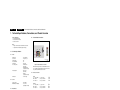
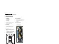
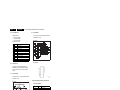
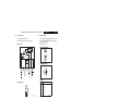
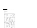
Colour Television
Chassis
TC8.1A
CA
H_17130_000.eps
240407
Contents
Page
1. Technical Specifications, Connections, and Chassis
Overview
2
2. Safety Instructions, Warnings, and Notes
4
3. Directions for Use
5
4. Mechanical Instructions
6
5. Service Modes, Error Codes, and Fault Finding 8
6. Block Diagrams, Test Point Overview, and
Waveforms
Block Diagram Mono Carrier
15
7. Circuit Diagrams and PWB Layouts
Mono Carrier
(A) 16
CRT Panel
(B) 19
Side AV & I/O Panel
(E) 21
8. Alignments
23
9. Circuit Descriptions, Abbreviation List, and IC Data
Sheets
28
Abbreviation List
33
10. Spare Parts List
34
11. Revision List
37
17-18
20
21
©
Copyright 2007 Philips Consumer Electronics B.V. Eindhoven, The Netherlands.
All rights reserved. No part of this publication may be reproduced, stored in a
retrieval system or transmitted, in any form or by any means, electronic,
mechanical, photocopying, or otherwise without the prior permission of Philips.
Published by WS 0764 BG CD Customer Service
Printed in the Netherlands
Subject to modification
EN 3122 785 17130
EN 2
1.
Technical Specifications, Connections, and Chassis Overview
TC8.1A CA
1. Technical Specifications, Connections, and Chassis Overview
1.2
Index of this chapter:
1.1 Technical Specifications
1.2 Side and Rear Connections
1.3 Chassis Overview
Side and Rear Connections
Notes:
• Figures can deviate due to the different set executions.
• Specifications are indicative (subject to change).
1.1
Technical Specifications
1.1.1
Vision
Display type
Screen size
Tuning system
Presets/channels
Tuner bands
TV colour systems
R
1.1.2
:
:
:
:
:
:
:
1.1.3
:
CRT, Real Flat
21” (55 cm), 4:3
PLL
100
Full-Cable
PAL B/G, D/K, I
(all models)
SECAM B/G, D/K
(only /56, /63, and /69)
NTSC, PAL
(all models)
SECAM
(only /56, /63, and /69)
75 ohm, F-type
H_17130_009.eps
240407
Figure 1-1 Rear and Side I/O connections
Note: The following connector colour abbreviations are used
(acc. to DIN/IEC 757): Bk= Black, Bu= Blue, Gn= Green, Gy=
Grey, Rd= Red, Wh= White, and Ye= Yellow.
1.2.1
Sound
Sound systems
Maximum power (WRMS)
: Stereo BTSC
: 1 x 5 or 2 x 5
(depending on model)
Miscellaneous
Power supply:
- Mains voltage (VAC)
- Mains frequency (Hz)
Ambient conditions:
- Temperature range (°C)
- Maximum humidity
VIDEO
Monitor out
:
Aerial input
L
AV1 in
:
Video playback
AUDIO
: 100 - 240
(/56 and /94)
: 180 - 240
(/63, /69, and /79)
: 50 / 60
: +5 to +40
: 90% R.H.
Power consumption (values are indicative)
- Normal operation (W)
: ≈ 70
- Stand-by (W)
: <7
1.2.2
Rear I/O Connections
AV In
Ye - Video (CVBS)
Wh - Audio - L
Rd - Audio - R
1 V_pp / 75 ohm
0.5 V_rms / 10 kohm
0.5 V_rms / 10 kohm
jq
jq
jq
AV Out
Ye - Video (CVBS)
Wh - Audio - L
Rd - Audio - R
1 V_pp / 75 ohm
0.5 V_rms / 10 kohm
0.5 V_rms / 10 kohm
kq
kq
kq
Aerial In
- F-type
Coax, 75 ohm
D
Side I/O Connections
AV In
Ye - Video (CVBS)
Wh - Audio - L
Rd - Audio - R
1 V_pp / 75 ohm
0.5 V_rms / 10 kohm
0.5 V_rms / 10 kohm
jq
jq
jq
Technical Specifications, Connections, and Chassis Overview
1.3
TC8.1A CA
1.
EN 3
Chassis Overview
B
CRT PANEL
D
SIDE AV PANEL +
HEADPHONE
MONO CARRIER
A
H_17130_039.eps
070507
Figure 1-2 PWB/CBA locations (depending on model)
EN 4
2.
TC8.1A CA
Safety Instructions, Warnings, and Notes
2. Safety Instructions, Warnings, and Notes
1. Perform the “general repair instruction” noted above.
2. Clean the power supply and deflection circuitry on the
chassis.
3. Clean the picture tube panel and the neck of the picture
tube.
Index of this chapter:
2.1 Safety Instructions
2.2 Maintenance Instructions
2.3 Warnings
2.4 Notes
2.1
Safety Instructions
2.3
Safety regulations require the following during a repair:
• Connect the set to the Mains/AC Power via an isolation
transformer (> 800 VA).
• Replace safety components, indicated by the symbol h,
only by components identical to the original ones. Any
other component substitution (other than original type) may
increase risk of fire or electrical shock hazard.
• Wear safety goggles when you replace the CRT.
•
Safety regulations require that after a repair, the set must be
returned in its original condition. Pay in particular attention to
the following points:
• General repair instruction: as a strict precaution, we advise
you to re-solder the solder connections through which the
horizontal deflection current flows. In particular this is valid
for the:
1. Pins of the line output transformer (LOT).
2. Fly-back capacitor(s).
3. S-correction capacitor(s).
4. Line output transistor.
5. Pins of the connector with wires to the deflection coil.
6. Other components through which the deflection current
flows.
Note: This re-soldering is advised to prevent bad connections
due to metal fatigue in solder connections, and is therefore only
necessary for television sets more than two years old.
• Route the wire trees and EHT cable correctly and secure
them with the mounted cable clamps.
• Check the insulation of the Mains/AC Power lead for
external damage.
• Check the strain relief of the Mains/AC Power cord for
proper function, to prevent the cord from touching the CRT,
hot components, or heat sinks.
• Check the electrical DC resistance between the Mains/AC
Power plug and the secondary side (only for sets that have
a Mains/AC Power isolated power supply):
1. Unplug the Mains/AC Power cord and connect a wire
between the two pins of the Mains/AC Power plug.
2. Set the Mains/AC Power switch to the "on" position
(keep the Mains/AC Power cord unplugged!).
3. Measure the resistance value between the pins of the
Mains/AC Power plug and the metal shielding of the
tuner or the aerial connection on the set. The reading
should be between 4.5 Mohm and 12 Mohm.
4. Switch "off" the set, and remove the wire between the
two pins of the Mains/AC Power plug.
• Check the cabinet for defects, to prevent touching of any
inner parts by the customer.
Warnings
V
E_06532_007.eps
250304
Figure 2-1 Discharge picture tube
•
•
•
•
Notes
2.4.1
General
•
Maintenance Instructions
We recommend a maintenance inspection carried out by
qualified service personnel. The interval depends on the usage
conditions:
• When a customer uses the set under normal
circumstances, for example in a living room, the
recommended interval is three to five years.
• When a customer uses the set in an environment with
higher dust, grease, or moisture levels, for example in a
kitchen, the recommended interval is one year.
• The maintenance inspection includes the following actions:
All ICs and many other semiconductors are susceptible to
electrostatic discharges (ESD w). Careless handling
during repair can reduce life drastically. Make sure that,
during repair, you are connected with the same potential as
the mass of the set by a wristband with resistance. Keep
components and tools also at this same potential.
Be careful during measurements in the high voltage
section.
Never replace modules or other components while the unit
is switched "on".
When you align the set, use plastic rather than metal tools.
This will prevent any short circuits and prevents circuits
from becoming unstable.
2.4
•
2.2
In order to prevent damage to ICs and transistors, avoid all
high voltage flashovers. In order to prevent damage to the
picture tube, use the method shown in figure “Discharge
picture tube”, to discharge the picture tube. Use a high
voltage probe and a multi-meter (position VDC). Discharge
until the meter reading is 0 V (after approx. 30 s).
•
Measure the voltages and waveforms with regard to the
chassis (= tuner) ground (H), or hot ground (I), depending
on the tested area of circuitry. The voltages and waveforms
shown in the diagrams are indicative. Measure them in the
Service Default Mode (see chapter 5) with a colour bar
signal and stereo sound (L: 3 kHz, R: 1 kHz unless stated
otherwise) and picture carrier at 475.25 MHz for PAL, or
61.25 MHz for NTSC (channel 3).
Where necessary, measure the waveforms and voltages
with (D) and without (E) aerial signal. Measure the
voltages in the power supply section both in normal
operation (G) and in stand-by (F). These values are
indicated by means of the appropriate symbols.
The semiconductors indicated in the circuit diagram and in
the parts lists, are interchangeable per position with the
semiconductors in the unit, irrespective of the type
indication on these semiconductors.
Directions for Use
2.4.2
•
•
•
•
•
2.4.3
All resistor values are in ohms, and the value multiplier is
often used to indicate the decimal point location (e.g. 2K2
indicates 2.2 kohm).
Resistor values with no multiplier may be indicated with
either an "E" or an "R" (e.g. 220E or 220R indicates 220
ohm).
All capacitor values are given in micro-farads (μ= x10-6),
nano-farads (n= x10-9), or pico-farads (p= x10-12).
Capacitor values may also use the value multiplier as the
decimal point indication (e.g. 2p2 indicates 2.2 pF).
An "asterisk" (*) indicates component usage varies. Refer
to the diversity tables for the correct values.
The correct component values are listed in the Spare Parts
List. Therefore, always check this list when there is any
doubt.
EN 5
Lead-free Soldering
Due to lead-free technology some rules have to be respected
by the workshop during a repair:
• Use only lead-free soldering tin Philips SAC305 with order
code 0622 149 00106. If lead-free solder paste is required,
please contact the manufacturer of your soldering
equipment. In general, use of solder paste within
workshops should be avoided because paste is not easy to
store and to handle.
• Use only adequate solder tools applicable for lead-free
soldering tin. The solder tool must be able:
– To reach a solder-tip temperature of at least 400°C.
– To stabilize the adjusted temperature at the solder-tip.
– To exchange solder-tips for different applications.
• Adjust your solder tool so that a temperature of around
360°C - 380°C is reached and stabilized at the solder joint.
Heating time of the solder-joint should not exceed ~ 4 sec.
Avoid temperatures above 400°C, otherwise wear-out of
tips will increase drastically and flux-fluid will be destroyed.
To avoid wear-out of tips, switch “off” unused equipment or
reduce heat.
• Mix of lead-free soldering tin/parts with leaded soldering
tin/parts is possible but PHILIPS recommends strongly to
avoid mixed regimes. If this cannot be avoided, carefully
clear the solder-joint from old tin and re-solder with new tin.
2.4.4
3.
B.O.M. (Bill Of Materials) that has been used for producing the
specific TV set. In general, it is possible that the same TV
model on the market is produced with e.g. two different types
of displays, coming from two different suppliers. This will then
result in sets which have the same CTN (Commercial Type
Number; e.g. 28PW9515/12) but which have a different B.O.M.
number.
By looking at the third digit of the serial number, one can
identify which B.O.M. is used for the TV set he is working with.
If the third digit of the serial number contains the number “1”
(example: BF1A063500001), then the TV set has been
manufactured according to B.O.M. number 1. If the third digit is
a “2” (example: BF2A0635000001), then the set has been
produced according to B.O.M. no. 2. This is important for
ordering the correct spare parts!
For the third digit, the numbers 1...9 and the characters A...Z
can be used, so in total: 9 plus 26= 35 different B.O.M.s can be
indicated by the third digit of the serial number.
Schematic Notes
•
TC8.1A CA
Alternative BOM identification
The third digit in the serial number (example:
BF2A0635000001) indicates the number of the alternative
3. Directions for Use
You can download this information from the following websites:
http://www.philips.com/support
http://www.p4c.philips.com
Identification: The bottom line of a type plate gives a 14-digit
serial number. Digits 1 and 2 refer to the production center (e.g.
AG is Bruges), digit 3 refers to the B.O.M. code, digit 4 refers
to the Service version change code, digits 5 and 6 refer to the
production year, and digits 7 and 8 refer to production week (in
example below it is 2006 week 17). The 6 last digits contain the
serial number.
MODEL
: 32PF9968/10
PROD.NO: AG 1A0617 000001
MADE IN BELGIUM
220-240V ~ 50/60Hz
128W
VHF+S+H+UHF
S
BJ3.0E LA
E_06532_024.eps
130606
Figure 2-2 Serial number (example)
2.4.5
Practical Service Precautions
•
•
It makes sense to avoid exposure to electrical shock.
While some sources are expected to have a possible
dangerous impact, others of quite high potential are of
limited current and are sometimes held in less regard.
Always respect voltages. While some may not be
dangerous in themselves, they can cause unexpected
reactions that are best avoided. Before reaching into a
powered TV set, it is best to test the high voltage insulation.
It is easy to do, and is a good service precaution.
EN 6
4.
Mechanical Instructions
TC8.1A CA
4. Mechanical Instructions
4.2
Index of this chapter:
4.1 Set Disassembly
4.2 Assy / Board Removal
4.3 Service Positions
4.4 Set Re-assembly
Sometimes, it can be necessary to swap a complete assy or
Printed Wiring Board (PWB). How that can be done is
explained below.
Note: Figures below can deviate slightly from the actual
situation, due to the different set executions.
4.1
Assy / Board Removal
4.2.1
Side IO/Keyboard Panel Removal
1. Remove the fixation screws [3].
2. Remove the module from the TV.
Set Disassembly
Follow the disassemble instructions in described order.
Rear Cover Removal
Warning: disconnect the mains power cord before you remove
the rear cover.
1. Remove all the fixation screws of the rear cover [1] and [2].
2. Now, pull the rear cover backwards and remove it.
3
2
4.1.1
1
1
1
H_17130_028.eps
070507
1
2
1
Figure 4-2 Side-IO/Keyboard panel removal (SYRF styling)
2
H_17130_036.eps
070507
Figure 4-1 Rear Cover removal (SL5 styling)
1
3
H_17130_040.eps
070507
Figure 4-3 Side-IO/Keyboard panel removal (SL5 styling)
Mechanical Instructions
4.2.2
TC8.1A CA
4.
EN 7
Mono Carrier Removal
1. First, disconnect the strain relief of the AC power cord [4].
2. Disconnect all the necessary cables [5].
3. To remove the Mono Carrier; release the clamps [6] and
slide the whole panel backwards [7] (= away from the
front).
4. Slide the panel away from the cabinet.
H_17130_023.eps
240407
Figure 4-7 Mono carrier removal [4/4]
4
1
4.3
For easy measurements, you can use the following service
position.
H_17130_025.eps
Figure 4-4 Mono carrier removal [1/4]
Service Positions
4.3.1
Service Position Mono Carrier
Removing cables and repositioning the panel
For better accessibility of the Mono Carrier, do the following
(see next figure):
1. If necessary, disconnect some cables, and move the panel
somewhat to the left. Then flip it 90 degrees with its
components towards the CRT.
5
1
H_17130_026.eps
Figure 4-5 Mono carrier removal [2/4]
H_17130_024.eps
240407
Figure 4-8 Service position Mono Carrier
6
1
7
1
Set Re-assembly
To re-assemble the whole set, do all processes in reverse
order.
Be sure that, before the rear cover is mounted:
• The mains cord is positioned correctly in its guiding
brackets (make sure that the strain relief is replaced in its
correct position and that it will function correctly!).
• All wires/cables are returned in their original positions.
6
1
H_17130_027.eps
Figure 4-6 Mono carrier removal [3/4]
4.4
EN 8
5.
TC8.1A CA
Service Modes, Error Codes, and Fault Finding
5. Service Modes, Error Codes, and Fault Finding
Index of this chapter:
5.1 Service Modes
5.2 Error Codes
5.3 Fault Finding
5.1
Service Modes
For an explanation of the Factory Mode, see chapter 8
“Alignments”.
5.2
Error Codes
Not applicable for this chassis.
5.3
Fault Finding
5.3.1
No Picture, No Sound, No Raster, Fuse Broken
No Picture, no sound, no raster, Fuse Broken
Is D833+
(B+)
Shorted to
earth?
YES
Check
(B+)
C of Q402
NO
Is D of Q801
Shorted to
to earth?
YES
Check
Q801
NO
Is D801D804
OK?
NO
Replace
D801-D804
YES
Check
IC 801
H_17130_010.eps
070507
Figure 5-1 Flow chart “No Picture, No Sound, No Raster, Fuse Broken”.
Service Modes, Error Codes, and Fault Finding
5.3.2
TC8.1A CA
5.
EN 9
No Picture, No Sound, No Raster, B+ OK
No Picture, no sound, no raster, B+ OK
Check
5V supply
pin 9 of IC 201
OK?
Yes
No
Check
H out waveform
Pin 13 of IC 201
OK?
Yes
No
Yes
Is IC201
Pin9 shorted to
earth ?
Check
waveform
C of Q401
OK?
Yes
No
Replace
IC 201
Replace
Q401or R401
Check
waveform
C of Q402
OK?
No
Replace
Q402
No
Check
+5V,+9V Circuit
H_17130_011.eps
070507
Figure 5-2 Flow chart “No Picture, No Sound, No Raster, B+ OK”.
5.3.3
No Picture, Raster and Sound OK
No Picture, Raster & Sound OK
Check RGB O/P
Pin 49,50,51,52
of IC 201 OK?
Yes
Check
RGB drive O/P
Q501, Q502 &
Q503
No
Is Pin ,50,51,52
shorted to
earth?
No
Check
9 volt Supply
& Q208
Yes
Replace
IC 201
Figure 5-3 Flow chart “No Picture, Raster and Sound OK”.
H_17130_012.eps
070507
EN 10
5.3.4
5.
TC8.1A CA
Service Modes, Error Codes, and Fault Finding
Picture OK, No Sound
Picture OK, No sound
Check Vcc
Pin 13 of IC601
OK?
No
Check +22v
Circuit
Yes
Check Vol
Pin 3 & Mute Pin10 of IC601 OK?
NO
Check
Q624,Q625,Q093 is
OK?
Yes
Check audio O/P
R & L of IC 601
OK?
No
Change the
damaged
component
Yes
Yes
Check
R & L speaker
No
Check
Pin 28,29 of
IC 201 OK?
Check
Pin 59 of IC 201
No
Check audio I/P
R & L of IC 601
OK?
Yes
Check
C601,R601,C602,
R602 OK?
No
Yes
Replace
IC 601
No
Change the
damaged
component
Replace
IC201
H_17130_013.eps
070507
Figure 5-4 Flow chart “Picture OK, No Sound”.
5.3.5
No Colour
No colour
Colour
system is
Right?
No
Reset
To
Local system
Yes
Dose the TV
signal too
weak?
NO
Check
Pin 6 & 7 of
IC 201 OK?
YES
Check
Tuner Input
cable & antenna
NO
Check
X001, C021
& C022
YES
Check
Pin 47 of IC
201
Figure 5-5 Flow chart “No Colour”.
H_17130_014.eps
070507
Service Modes, Error Codes, and Fault Finding
5.3.6
TC8.1A CA
5.
EN 11
One Horizontal Line
One horizontal line
Check
Deflection yoke
Terminal OK?
Yes
Check
+24v supply
Pin 2 of IC 301
OK?
No
Replace
Yoke coil
No
Check
R405 (Fuse)
D402
No
Check
V input
Pin 1 of IC 301
OK?
Yes
Check
V output
Pin 5 of IC 301
OK?
No
Yes
Check
R314, C301,
R317,R336, C309
Check
V output
Pin 16 of IC 201
Figure 5-6 Flow chart “One Horizontal Line”.
H_17130_015.eps
070507
EN 12
5.3.7
5.
TC8.1A CA
Service Modes, Error Codes, and Fault Finding
Some Waveforms:
H_17130_019.eps
240407
H_17130_016.eps
240407
Figure 5-10 V-out pin 5 of IC301
Figure 5-7 FBP pin 12 of IC201
H_17130_020.eps
240407
H_17130_017.eps
240407
Figure 5-11 Q402 C
Figure 5-8 H_out pin 13 of IC201
H_17130_021.eps
240407
H_17130_018.eps
240407
Figure 5-9 V-out pin 16 of IC201
Figure 5-12 Q815 drain when stand-by
Service Modes, Error Codes, and Fault Finding
H_17130_022.eps
240407
Figure 5-13 Q815 drain
5.3.8
Important Voltages Overview
Line
Position
1
B+ Joint of L801 and R826A +110.8
Normal (V) Standby (V)
+96.9
2
Joint of C834 and D831
+13.0
+10.9
3
Joint of L212 and C090
+5.0
+0.0
4
Pin99 of IC200
+4.8
+0.0
TC8.1A CA
5.
EN 13
Block Diagrams, Test Point Overview, and Waveforms
TC8.1A CA
6.
15
6. Block Diagrams, Test Point Overview, and Waveforms
Block Diagram Mono Carrier
220V~
Q815,IC801
AMP.
D801—D804
T803
Transformer
112(108)v
22V
12V
Power
R/G/B
AGC
Tuner
TU101
Toshiba
IF AMP
Q101
SAW
R/G/B
CRT
V. AMP.
IC301
EHT
FOCUS
SCREEN
8891\8893
IC201
E2PROM
IC001
Signal Process
V.out
Video Amp.
H.out
H. drive AMP.
Q401 Q402
KEY
IR001
Sensor
Audio AMP.
FBT
T402
175V, 24V
Speaker
IC601
AV Vin
AV Vout
H_17130_008.eps
160407
Circuit Diagrams and PWB Layouts
TC8.1A CA
7.
16
7. Circuit Diagrams and PWB Layouts
Mono Carrier
A
MONO CARRIER
A
H_17130_001.eps
160407
Circuit Diagrams and PWB Layouts
TC8.1A CA
7.
17
Layout Mono Carrier (Top Side)
H_17130_002.eps
160407
Circuit Diagrams and PWB Layouts
TC8.1A CA
7.
18
Layout Mono Carrier (Bottom Side)
H_17130_003.eps
160407
Circuit Diagrams and PWB Layouts
TC8.1A CA
7.
19
CRT Panel
1
B
2
3
4
5
6
7
8
9
10
CRT PANEL
B
A
A
B
B
C
C
D
D
E
E
F
F
G
G
H_17130_004.eps
160407
1
2
3
4
5
6
7
8
9
10
Circuit Diagrams and PWB Layouts
TC8.1A CA
7.
20
Layout CRT Panel (Top Side)
Personal Notes:
H_17130_005.eps
160407
E_06532_012.eps
131004
Circuit Diagrams and PWB Layouts
TC8.1A CA
7.
21
Side AV & I/O Panel
5
D
Personal Notes:
4
SIDE AV I/O PANEL
D
D
D
C
C
Main Board
Main Board
H_17130_006.eps
160407
5
4
Layout Side AV & I/O Panel (Top Side)
H_17130_007.eps
160407
E_06532_012.eps
131004
Alignments
8. Alignments
Index of this chapter:
8.1 General Information
8.2 Factory Mode (Service Menu, Service Mode)
8.3 Alignment procedure
Note: Figures below can deviate slightly from the actual
situation, due to the different set executions.
8.1
General Information
Perform all electrical adjustments under the following
conditions:
• Power supply voltage: 100 - 240 VAC, 50/60 Hz (± 10%)
• Connect the set to the mains via an isolation transformer
with low internal resistance.
• Allow the set to warm up for approximately 15 minutes.
• Measure voltages and waveforms in relation to correct
ground (e.g. measure audio signals in relation to
AUDIO_GND).
Caution: It is not allowed to use heatsinks as ground.
• Test probe: Ri > 10 Mohm, Ci < 20 pF.
• Use an isolated trimmer/screwdriver to perform
alignments.
8.2
Factory Mode (Service Menu, Service Mode)
For certain alignment procedures, you will need to enter
Factory Mode (Service Menu). See also figure ““ on next
page.
8.2.1
How To Enter
1. Press and hold the VOLUME DOWN key on the TV tightly
until minimum level.
2. Then, while holding the VOLUME DOWN key, press the
“DEL / [i+]” key on the remote control (RC).
8.2.2
How To Navigate
•
•
•
•
8.2.3
Press “CH+ (^) / CH- (v)” cursor key on the RC to select
option.
Press “VOL- (<) / VOL+ (>)” cursor key on the RC to adjust
or select option.
Press “0-9” or “SOUND SYS” key on the RC as the shortcut
key to directly access certain factory menu’s (see figure
“Group list overview”).
All changes in factory data will be saved in EEPROM
automatically.
How To Exit
Press the RC “POWER / F” button, or power down the set with
the main switch, to exit the Factory Mode.
TC8.1A CA
8.
EN 23
EN 24
8.2.4
8.
Alignments
TC8.1A CA
Factory Mode Overview
Navigation:
CH-
CH+
V8-TM28-5669 ver. x.x
OEMV
17
V8-TM28-5669 ver. x.x
STBG
8
V8-TM28-5669 ver. x.x
VCENP
12
V8-TM28-5669 ver. x.x
SBY
8
V8-TM28-5669 ver. x.x
SVD
18
V8-TM28-5669 ver. x.x
OPT
86
V8-TM28-5669 ver. x.x
OEMH
12
V8-TM28-5669 ver. x.x
OSDF2
64
V8-TM28-5669 ver. x.x
VBLK
0
V8-TM28-5669 ver. x.x
VSS
15
V8-TM28-5669 ver. x.x
SV4
20
V8-TM28-5669 ver. x.x
OSD1
12
V8-TM28-5669 ver. x.x
OEMC
7
V8-TM28-5669 ver. x.x
OSD2
1B
V8-TM28-5669 ver. x.x
SVM
0
V8-TM28-5669 ver. x.x
VLIS
13
V8-TM28-5669 ver. x.x
ST4
1B
V8-TM28-5669 ver. x.x
MISHA
3C
V8-TM28-5669 ver. x.x
CBDRV
08
V8-TM28-5669 ver. x.x
OSDF1
5A
V8-TM28-5669 ver. x.x
STBY
7F
V8-TM28-5669 ver. x.x
VSC
15
V8-TM28-5669 ver. x.x
SV3
20
V8-TM28-5669 ver. x.x
MITIN
32
V8-TM28-5669 ver. x.x
CGDRV
81
V8-TM28-5669 ver. x.x
AOPT
0
V8-TM28-5669 ver. x.x
MOD
0
V8-TM28-5669 ver. x.x
VLIN
10
V8-TM28-5669 ver. x.x
ST3
1B
V8-TM28-5669 ver. x.x
MICOL
35
V8-TM28-5669 ver. x.x
CBCUT
01
V8-TM28-5669 ver. x.x
OSDHS
1B
V8-TM28-5669 ver. x.x
VBK
8
V8-TM28-5669 ver. x.x
HITS
16
V8-TM28-5669 ver. x.x
TNTN
4A
V8-TM28-5669 ver. x.x
MIBRI
32
V8-TM28-5669 ver. x.x
CGCUT
03
V8-TM28-5669 ver. x.x
OSDH
25
V8-TM28-5669 ver. x.x
UBK
8
V8-TM28-5669 ver. x.x
VP60
0
V8-TM28-5669 ver. x.x
TNTX
4A
V8-TM28-5669 ver. x.x
MICON
4B
V8-TM28-5669 ver. x.x
CRCUT
02
V8-TM28-5669 ver. x.x
NDTCT
5
V8-TM28-5669 ver. x.x
VCD0
0
V8-TM28-5669 ver. x.x
HPS
0E
V8-TM28-5669 ver. x.x
COLN
12
V8-TM28-5669 ver. x.x
STSHA
3C
V8-TM28-5669 ver. x.x
WBDRV
8D
V8-TM28-5669 ver. x.x
NDTC
5
V8-TM28-5669 ver. x.x
VCD1
41
V8-TM28-5669 ver. x.x
HIT
16
V8-TM28-5669 ver. x.x
COLX
1B
V8-TM28-5669 ver. x.x
STTIN
32
V8-TM28-5669 ver. x.x
WGDRV
85
V8-TM28-5669 ver. x.x
NOIS
1
V8-TM28-5669 ver. x.x
FLG1
(see delta NVM list)
V8-TM28-5669 ver. x.x
VP50
3
V8-TM28-5669 ver. x.x
BRTN
40
V8-TM28-5669 ver. x.x
STCOL
3A
V8-TM28-5669 ver. x.x
WBCUT
06
V8-TM28-5669 ver. x.x
HD DELAY
0C
V8-TM28-5669 ver. x.x
FLG0
6
V8-TM28-5669 ver. x.x
HPOS
0A
V8-TM28-5669 ver. x.x
BRTX
40
V8-TM28-5669 ver. x.x
STBRI
3C
V8-TM28-5669 ver. x.x
WGCUT
04
V8-TM28-5669 ver. x.x
MODE2
19
V8-TM28-5669 ver. x.x
STAT
0
V8-TM28-5669 ver. x.x
BBCT
4
V8-TM28-5669 ver. x.x
CNTN
28
V8-TM28-5669 ver. x.x
STCON
5C
V8-TM28-5669 ver. x.x
WRCUT
02
V8-TM28-5669 ver. x.x
MODE1
(see delta NVM list)
V8-TM28-5669 ver. x.x
MUTT
0
V8-TM28-5669 ver. x.x
AKB
3
V8-TM28-5669 ver. x.x
CNTC
37
V8-TM28-5669 ver. x.x
DYSHA
3C
V8-TM28-5669 ver. x.x
FM RADIO
80
V8-TM28-5669 ver. x.x
MODE0
(see delta NVM list)
V8-TM28-5669 ver. x.x
V100
76
V8-TM28-5669 ver. x.x
DEF
1
V8-TM28-5669 ver. x.x
SCNT
08
V8-TM28-5669 ver. x.x
DYTIN
32
V8-TM28-5669 ver. x.x
SYSR
(see delta NVM list)
V8-TM28-5669 ver. x.x
PYNS
1E
V8-TM28-5669 ver. x.x
V90
75
V8-TM28-5669 ver. x.x
CLVD
8
V8-TM28-5669 ver. x.x
VCD2
34
V8-TM28-5669 ver. x.x
DYCOL
30
V8-TM28-5669 ver. x.x
SYBBF
20
V8-TM28-5669 ver. x.x
PYXS
22
V8-TM28-5669 ver. x.x
V80
74
V8-TM28-5669 ver. x.x
CLV0
2F
V8-TM28-5669 ver. x.x
COLS
33
V8-TM28-5669 ver. x.x
DYBRI
44
V8-TM28-5669 ver. x.x
SYBBN
20
V8-TM28-5669 ver. x.x
PYNN
18
V8-TM28-5669 ver. x.x
V50
(see delta NVM list)
V8-TM28-5669 ver. x.x
CLTM
2C
V8-TM28-5669 ver. x.x
COLP
0B
V8-TM28-5669 ver. x.x
DYCON
5F
V8-TM28-5669 ver. x.x
NOIS DET
0F
V8-TM28-5669 ver. x.x
PYNX
28
V8-TM28-5669 ver. x.x
V40
(see delta NVM list)
V8-TM28-5669 ver. x.x
CLTD
5
V8-TM28-5669 ver. x.x
TNTC
3C
V8-TM28-5669 ver. x.x
SECD
90
V8-TM28-5669 ver. x.x
SYNC DET
2
V8-TM28-5669 ver. x.x
UCOM
20
V8-TM28-5669 ver. x.x
V30
(see delta NVM list)
V8-TM28-5669 ver. x.x
CLTB
5
V8-TM28-5669 ver. x.x
COLC
28
V8-TM28-5669 ver. x.x
UVBDRV
0
V8-TM28-5669 ver. x.x
SSM
0
V8-TM28-5669 ver. x.x
EHT
24
V8-TM28-5669 ver. x.x
V10
(see delta NVM list)
V8-TM28-5669 ver. x.x
DCBS
13
V8-TM28-5669 ver. x.x
BRTC
2D
V8-TM28-5669 ver. x.x
UVGDRV
0
V8-TM28-5669 ver. x.x
SSDK
0
V8-TM28-5669 ver. x.x
ECCB
10
V8-TM28-5669 ver. x.x
V05
(see delta NVM list)
V8-TM28-5669 ver. x.x
ABL
27
V8-TM28-5669 ver. x.x
CNTX
47
V8-TM28-5669 ver. x.x
UVBCUT
0
V8-TM28-5669 ver. x.x
SSI
0
V8-TM28-5669 ver. x.x
ECCT
10
V8-TM28-5669 ver. x.x
V01
0F
V8-TM28-5669 ver. x.x
RGCN
0
V8-TM28-5669 ver. x.x
BD
40
V8-TM28-5669 ver. x.x
UVGCUT
0
V8-TM28-5669 ver. x.x
SSBG
0
V8-TM28-5669 ver. x.x
TRUM
20
V8-TM28-5669 ver. x.x
HAFC
86
V8-TM28-5669 ver. x.x
TXCX
1F
V8-TM28-5669 ver. x.x
GD
40
V8-TM28-5669 ver. x.x
UVRCUT
0
V8-TM28-5669 ver. x.x
STM
8
V8-TM28-5669 ver. x.x
PRBR
20
V8-TM28-5669 ver. x.x
RF AGC
20
V8-TM28-5669 ver. x.x
SHPN
14
V8-TM28-5669 ver. x.x
BB
65
V8-TM28-5669 ver. x.x
HBP
44
V8-TM28-5669 ver. x.x
STDK
8
V8-TM28-5669 ver. x.x
HSIZ
20
V8-TM28-5669 ver. x.x
BRTS
13
V8-TM28-5669 ver. x.x
SHPX
7
V8-TM28-5669 ver. x.x
GB
65
V8-TM28-5669 ver. x.x
OEMVS
8
V8-TM28-5669 ver. x.x
STI
8
V8-TM28-5669 ver. x.x
VCENN
15
V8-TM28-5669 ver. x.x
SRY
8
V8-TM28-5669 ver. x.x
ASSH
5
V8-TM28-5669 ver. x.x
RB
65
START (Factory Mode)
Back to START
Parameter not included
in the group menu
H_17130_038.eps
070507
Figure 8-1 Factory mode overview (incl. default values)
Alignments
8.2.5
TC8.1A CA
8.
EN 25
Group List Overview
GROUP1
RB
GB
BB
GD
BD
UBK
VBK
GROUP2
HPOS
HPS
HIT
HITS
VP50
VP60
VLIN
VLIS
VSC
VSS
VBLK
VCENP
VCENN
OSDH
OSDHS
GROUP 3
CNTX
CNTN
BRTX
BRTN
COLX
COLN
TNTX
TNTN
GROUP 4
BRTC
COLC
COLS
COLP
SCNT
CNTC
TNTC
GROUP 5
ST3
SV3
ST4
SV4
SVD
ASSH
SHPX
SHPN
GROUP 6
OPT
KEY 0
R CUT OFF
G CUT OFF
B CUT OFF
G DRIVE
B DRIVE
DVD U level adjustment
0: (-22mV, Input DC)
8: 0mV
F: (19mV, 2.75mV/dev)
DVD V level adjustment
Bits 4-7 Don’t use
KEY 1
Horizontal Position 50Hz
Horizontal Position 60Hz
Height 50Hz
Height 60 Hz
Vertical Position 50Hz
Vertical Position 60Hz
V Linearity 50Hz
V Linearity 60hz
VS Correction 50Hz
VS Correction 60Hz
V BLK Start / Stop
V CENTERING 50Hz
V CENTERING 60Hz
OSD vertical position 50Hz
OSD vertical position 60Hz
KEY 3
CONTRAST MAX.
CONTRAST MIN.
BRIGHT MAX. (difference from center)
BRIGHT MIN. (difference from center)
COLOR MAX. (difference from center)
COLOR MIN.
TINT MAX. (difference from center)
TINT MIN. (difference from center)
KEY 4
BRIGHT CENTER
COLOR CENTER NTSC
COLOR CENTER SECAM
COLOR CENTER PAL (shift data from COLC)
SUB CONTRAST
CONTRAST CENTER
TINT CENTER
KEY 5
SHARP CENTER 3.58NTSC TV
SHARP CENTER 3.58NTSC VIDEO
SHARP CENTER OTHER TV
SHARP CENTER OTHER VIDEO
SHARP CENTER DVD
ASYMMETRY-SHARPNESS
SHARP MAX. (difference from center)
SHARP MIN. (difference from center)
KEY 6
OPTION DATA
0 D mode key 0: No use 1 :use
1 0:normal 1: mute sound when no sync in TV
2 0:NORMAL 1: mute video during change channel
3 AU gain (0: 50kHz 1: 25kHz)
4 when no sync (1: AFT 0: no AFT)
5 AV change (1:mute 0:no mute)
6 Korea PAL50 blink function (1:enable 0:disable)
7 Standby state (0:High standby 1:Low standby)
FLG0
0
1
2
3
4
5
6
7
Over MOD
N Buzz Cancel
Pin 56 function (1: AV1/AV2 0:Mute pin)
SLO f0 shift
Hotel mode TV mode enter
Hotel mode AV mode enter
Hotel mode
VCO readjust when position select (0:enable 1:disable)
FLG1
0
1
2
3
4
5
6
7
(0: 6 key 1: 7 key)
OEM Logo (0: Use TCL Logo 1: Use OEM Logo)
Logo (0: disable 1: enable)
TINT por
PIF SELECT 00: 38MHz
01: 38.9MHz
10:45.75MHz 11:Don’t Use
SECAM (0:disable 1:enable)
APC (0:Preset 1:Auto)
STBY
0
1
2
3
4
5
6
7
Not Used
Not Used
HD kill timer set *40us
Not Used
When STBY.5=0 ,after AC on 0: standby 1: power on
After AC power on, 0: ref STBY4
1: last state
Biological Clock (0:disable 1:enable)
Child Lock (1:diable 0:enable)
0
1
2
3
4
5
6
7
FS/VS Select 0:VS TUNER 1:FS Tuner
English language select
Arabic language select /Thailand
Vietnam language select
Mute type 0: y mute 1: RGB mute
When mode0. (7 = 1 ; preset sound system after ASM)
00:BG 01:I 10:DK 11:M
Preset sound system after ASM (0:disable 1:enable)
MODE1
0
1
2
3
4
5
6
7
BG system enable
I system enable
DK system enable
M system enable
Video2 enable
Video3 enable
YUV enable
Thailand Dual language 0:Disable 1:Enable
MUTT
STAT
Standby -->wake time
Contrast up timer after standby off
HD DELAY
MODE0
GROUP 7
RFAGC
SBY
SRY
BRTS
TXCX
RGCN
BBCT
GROUP 9
V01
V05
V10
V30
V40
V50
V70
V90
V100
GROUP 10
SVM
PYNX
PYNN
PYXS
PYNS
GROUP 16
STBG
STI
STDK
STM
SSBG
KEY 7
RF AGC
SECAM B-Y BLACK ADJUST
SECAM R-Y BLACK ADJUST
SUB BRIGHT shift data of BRTC
TEXT RGB CONTRAST MAX.
TEXT RGB CONTRAST MIN.
SECAM MODE
KEY 8
VOLUME 01
VOLUME 05
VOLUME 10
VOLUME 30
VOLUME 40
VOLUME 50
VOLUME 70
VOLUME 90
VOLUME 100
KEY 9
SVM
Normal H.SYNC max
Normal H.SYNC min
Search H.SYNC max
Search H.SYNC min
KEY 2
0~3 (S-Trap f0 for BG) [0: Sound Trap Off 1: f0 tuning min F: f0 tuning max]
4~7 (Don’t use)
0~3 (S-Trap f0 for I) [0: Sound Trap Off 1: f0 tuning min F: f0 tuning max]
4~7 (Don’t use)
0~3 (S-Trap f0 for DK) [0: Sound Trap Off 1: f0 tuning min F: f0 tuning max]
4~7 (Don’t use)
0~3 (S-Trap f0 for I) [0: Sound Trap Off 1: f0 tuning min F: f0 tuning max]
4~7 (Don’t use)
0~1 - Sound Trap GD for BG [00: Off 01: 60nS 10: 90nS 11: 120nS]
2~3 - Sound Trap Q for BG [00: Q = 3 01: Q = 5 10: Q = 7 11: Q = 9]
4~5 - Sound Trap HP/LP for BG [00: Off 01: 1 dB HPF 10: -3 dB LPF 11: -2 dB LPF]
6~7 (Don’t use)
SSI
0~1 - Sound Trap GD for I [00: Off 01: 60nS 10: 90nS 11: 120nS]
2~3 - Sound Trap Q for I [00: Q = 3 01: Q = 5 10: Q = 7 11: Q = 9]
4~5 - Sound Trap HP/LP for I [00: Off 01: 1 dB HPF 10: -3 dB LPF 11: -2 dB LPF]
6~7 (Don’t use)
SSDK
0~1 (Sound Trap GD for DK) [00: Off 01: 60nS 10: 90nS 11: 120nS]
2~3 (Sound Trap Q for DK) [00: Q = 3 01: Q = 5 10: Q = 7 11: Q = 9]
4~5 (Sound Trap HP/LP for DK) [00: Off 01: 1 dB HPF 10: -3 dB LPF 11: -2 dB LPF]
6~7 (Don’t use)
SSM
0~1 (Sound Trap GD for M ) [00: Off 01: 60nS 10: 90nS 11: 120nS]
2~3 (Sound Trap Q for M) [00: Q = 3 01: Q = 5 10: Q = 7 11: Q = 9]
4~5 (Sound Trap HP/LP for M) [00: Off 01: 1 dB HPF 10: -3 dB LPF 11: -2 dB LPF]
6~7 (Don’t use)
GROUP 17
NDTC
NDTCT
OEMC
OEMH
OEMV
OEMVS
HBP
Key SNDSYS
0~7 (Counter for non-weak signal detection) [0 - FF]
0~7 (Counter for weak signal detection) [0 - FF]
0~2 (OEM Logo string color setting) [000: Black 001: use Red instead of Blue 010: Green
011: Cyan 100: Red 101: Magenda
110: Yellow 111: White]
3~7 (Don’t use)
0~7 (H - offset value for OEM logo) [0 - FF]
0 - 7 (V – offset value for OEM logo in 50Hz system) [0 - FF]
0 - 7 (V – offset value for OEM logo in 60Hz system) [0 - FF]
0 - 3 (H BOW) [0: -1uS 4: 0uS 7: 1uS] [0: -/+2 Us 4: 0 uS 7: +/-2 uS]
4~7 (H PARA)
H_17130_037.eps
070507
Figure 8-2 Group list overview
EN 26
Alignments
TC8.1A CA
Delta NVM Overview
Some option values depend on the model number. Please refer
to table below for the deviations.
6
8
13
6
9
15
21PT5007/56
21PT2327/69
21PT5027/69
21PT5007/69
21PT5027/94
21PT5017/94
21PT2217/94
21PT5007/94
Option
21PT5027/56
Group
21PT2327/56
Key
21PT5027/79
Table 8-1 Delta NVM overview
21PT2327/79
8.2.6
8.
OPT
0x86
0x86
0x86
0x86
0x86
0x86
0x86
0x86
0x86
0x86
0x86
0x86
FLG0
0x06
0x06
0x06
0x06
0x06
0x06
0x06
0x06
0x06
0x06
0x06
0x06
FLG1
0x9C
0x9C
0x9C
0x9C
0xDC
0xDC
0xDC
0xDC
0xDC
0xDC
0x9C
0x9C
STBY
0x7F
0x7F
0x7F
0x7F
0x7F
0x7F
0x7F
0x7F
0x7F
0x7F
0x7F
0x7F
HD DELAY
0x0C
0x0C
0x0C
0x0C
0x0C
0x0C
0x0C
0x0C
0x0C
0x0C
0x0C
0x0C
MODE0
0x93
0x93
0x93
0x93
0x9B
0x9B
0x9B
0x97
0x97
0x97
0x93
0x93
MODE1
0x17
0x07
0x17
0x17
0x17
0x17
0x07
0x17
0x17
0x07
0x17
0x07
MUTT
0x00
0x00
0x00
0x00
0x00
0x00
0x00
0x00
0x00
0x00
0x00
0x00
STAT
0x00
0x00
0x00
0x00
0x00
0x00
0x00
0x00
0x00
0x00
0x00
0x00
V01
0x0F
0x0F
0x0F
0x0F
0x0F
0x0F
0x0F
0x0F
0x0F
0x0F
0x0F
0x0F
V05
0x0F
0x0F
0x0F
0x0F
0x12
0x12
0x12
0x12
0x12
0x12
0x12
0x12
V10
0x15
0x15
0x15
0x15
0x17
0x17
0x17
0x17
0x17
0x17
0x17
0x17
V30
0x49
0x49
0x49
0x49
0x28
0x28
0x28
0x28
0x28
0x28
0x28
0x28
V40
0x58
0x58
0x58
0x58
0x3C
0x3C
0x3C
0x3C
0x3C
0x3C
0x3C
0x3C
V50
0x63
0x63
0x63
0x63
0x53
0x53
0x53
0x53
0x53
0x53
0x53
0x53
V80
0x74
0x74
0x74
0x74
0x74
0x74
0x74
0x74
0x74
0x74
0x74
0x74
V90
0x75
0x75
0x75
0x75
0x75
0x75
0x75
0x75
0x75
0x75
0x75
0x75
V100
0x76
0x76
0x76
0x76
0x76
0x76
0x76
0x76
0x76
0x76
0x76
0x76
VCD0
0x00
0x00
0x00
0x00
0x00
0x00
0x00
0x00
0x00
0x00
0x00
0x00
VCD1
0x41
0x41
0x41
0x41
0x41
0x41
0x41
0x41
0x41
0x41
0x41
0x41
VCD2
0x34
0x34
0x34
0x34
0x34
0x34
0x34
0x34
0x34
0x34
0x34
0x34
MODE2
0x15
0x15
0x15
0x15
0x15
0x15
0x15
0x15
0x15
0x15
0x15
0x15
0x02
SYNC DET
0x02
0x02
0x02
0x02
0x02
0x02
0x02
0x02
0x02
0x02
0x02
SYBBN
0x20
0x20
0x20
0x20
0x20
0x20
0x20
0x20
0x20
0x20
0x20
0x20
SYBBF
0x20
0x20
0x20
0x20
0x20
0x20
0x20
0x20
0x20
0x20
0x20
0x20
SYSR
0x20
0x20
0x20
0x20
0x10
0x10
0x10
0x10
0x10
0x10
0x10
0x10
NOIS DET
0x0F
0x0F
0x0F
0x0F
0x0F
0x0F
0x0F
0x0F
0x0F
0x0F
0x0F
0x0F
Alignments
8.3
Alignment procedure
Perform the alignments in the following sequence:
1. B+ voltage adjustment.
2. RF AGC adjustment.
3. Screen voltage and focus adjustment.
4. White balance adjustment.
5. Pin cushion and screen width adjustment.
6. Screen centre and size adjustment (PAL).
7. Screen centre and size adjustment (NTSC).
8.3.1
B+ Voltage Test
1. Apply the specified mains voltage to the mains power input,
and a standard test pattern to the RF input.
2. Not need to adjust, just for verification: with the TV settings
in “Personal” mode (BRI/CONT/COL in middle position),
test if the voltage at D833 (B+) is 112 V ± 2.0 V.
8.3.2
RF AGC Adjustment
1. Input RF signal: 80 dBμV Color Bar signal, 100%
modulation (e.g. PM5418, RF Ampl.: 10 mV).
2. Press key “7” on the RC (in Factory Mode) to enter the RF
AGC adjustment mode.
3. Adjust the “RFAGC” item until the output of the detector
becomes 0.6 Vp-p ± 0.05 V.
8.3.3
8.3.5
8.
EN 27
with “WRCUT“, “WGCUT“, “WBCUT“, “WGDRV“, and
“WBDRV“, while the WARM adjustments can be performed
via “CRCUT“, “CGCUT“, “CBCUT“, “CGDRV“, and
“CBDRV“
When adjusting, “BB” and “GB” are used to adjust black
balance, and “BD” and “GD” are used to adjust white
balance.
Picture geometric adjustment
For PAL
1. Input a PAL cross hatch pattern (in NATURAL status).
2. Press key “1” on the RC (in Factory Mode) to enter the
Geometric adjustment.
3. Select “HPOS” to adjust the horizontal centre.
4. Select “VP50” to adjust the vertical centre.
5. Select “HIT” to adjust the vertical amplitude.
6. Select “VLIN” to adjust the vertical linearity.
7. Select “VSC” to adjust the vertical S-correction.
For NTSC
1. Input a NTSC cross hatch pattern (in NATURAL status).
2. Press key “1” on the RC (in Factory Mode) to enter the
Geometric adjustment.
3. Select “HPS” to adjust the horizontal center.
4. Select “VP60” to adjust the vertical center.
5. Select “HITS” to adjust the vertical amplitude.
6. Select “VLIS” to adjust the vertical linearity.
7. Select “VSS” to adjust the vertical S-correction.
Focus and Screen Voltage Adjustment
1. Before adjusting, please confirm that the settings are:
– Input signal: Cross Hatch test pattern
– SMART PICTURE = NATURAL.
2. Adjust the “FOCUS” potentiometer on the LOT such that
the horizontal/vertical line of 2/3 on the screen looks
thinnest. The FOCUS voltage must be within 6.6 - 7.8 kV.
3. Then adjust the “SCREEN” potentiometer on the LOT until
the horizontal line is just visible.
4. At this moment (vertical “off”), measure the VG2 voltage
with a high voltage meter and high voltage test probe
(1000:1). The VG2 voltage spec is 570 V ± 50 V.
8.3.4
•
TC8.1A CA
White Balance Adjustment
1. Before adjusting, please confirm that the settings are:
– Input signal: Black and White test pattern
– SMART PICTURE = NATURAL.
– COLOR TEMP= NORMAL.
2. Press key “0” on the RC (in Factory Mode) to enter the
White Balance adjustment mode.
3. Use a color analyser to measure the Black part of the
screen. By changing the value of “BB” and “GB”, set the
reading of the color analyser to the x,y values as given in
the next table.
4. Use a color analyser to measure the White part of the
screen. By changing the value of “BD” and “GD”, set the
reading of the color analyser to the x,y values as given in
the next table.
5. Repeat these steps until you get the right color on both dark
and bright pictures (see next table).
Table 8-2 White balance adjustment values
Picture Mode
Color Temp. x
11500K
274
y
Y (Nit)
280
90 (white), 5 (black)
Cool
15000K
265 *
266 *
Warm
8500K
291 *
300 *
Normal
Remarks:
• (*) Only adjust the NORMAL status; the COOL and WARM
offset adjustments are preset in the NVM.
If necessary, the COOL adjustments can be performed
Adjustment of OSD Position
1. Navigate through the “Factory Mode” options with the “CH+
(^) / CH- (v)” cursor keys on the RC (see also figure
“Factory Mode Overview”).
2. Select the “OSD2” option and adjust the OSD horizontal
position, until OSD “MUTE” is at the middle of the screen.
EN 28
9.
Circuit Descriptions, Abbreviation List, and IC Data Sheets
TC8.1A CA
9. Circuit Descriptions, Abbreviation List, and IC Data Sheets
Index of this chapter:
9.1 General
9.2 Chassis Block Diagram
9.3 Brief IC Descriptions
9.4 Abbreviation List
Notes:
• Figures can deviate slightly from the actual situation, due
to different set executions.
• For a good understanding of the following circuit
descriptions, please use the Wiring, Block (chapter 6) and
Circuit Diagrams (chapter 7). Where necessary, you will
find a separate drawing for clarification.
9.1
General
This chassis uses the Toshiba TPMA8891 processor/decoder,
and has the following key components:
Item
Part No.
Name of IC
Function
IC201
13-PA8891-PSP
TMPA8891CXBNG
MCU & Decoder
TU101 07-389FI5-NA3G
9.2
FSBP05P-3-E
Tuner
Z101
45-SAW296-6M00G K2966M
SAW Filter
IC001
13-24C08A-PUP27
AT24C08A
EEPROM
IC601
13-TDA749-6AS
TDA7496SA
Audio output amplifier
IC901
13-000040-53P
HCF4053B
Analog Switch
IC301
13-LA7804-0NS
LA78040N-E
Vertical Deflection Output IC
Q402
11-4508DZ-0CX
BU4508DZS
Horizontal Output IC
IC801
13-TEA150-6PP
TEA1506P
Power Controller IC
Chassis Block Diagram
Below find the chassis block diagram:
AV1
AV2
AV output
TDA7496
SA
4053BP
TUNER
( IC901)
(IC601)
( TU101)
Video &
Audio
SAWF
Audio
( Z101)
R
Decoder & MCU
TMPA8891
G
(IC201)
B
SDA
CRT
SCL
EEPROM
( IC001)
CRT
Board
Horizontal
Output circuit
+24V
Vertical Output
LA7804
( IC301)
H_17130_034.eps
240407
Figure 9-1 Chassis block diagram
Circuit Descriptions, Abbreviation List, and IC Data Sheets
9.3
Brief IC Descriptions
9.3.1
IC201 (TMPA8891CXBNG)
TC8.1A CA
9.
EN 29
The TMPA8891 is an integrated circuit for a PAL/ NTSC/
SECAM TV. A microcontroller (MCU) and a TV signal
processor are integrated in a 64-pin shrink DIP package.
The MCU part contains:
• 8-bit CPU.
• ROM.
• RAM.
• I/O ports.
• Timers/ counters.
• A/D converters.
• On-Screen Display controller.
• remote control interfaces.
• IIC bus interfaces.
• Closed Caption decoder.
The TV signal processor part contains:
• PIF.
• SIF.
• Video.
• Multi-standard chroma.
• Sync.
• RGB processors.
Block diagram is as follows:
49
48
47
45
44
43
42
41
39
40
I/O
10 I/O port
14-bit PWM x1
7-bit PWM x1
8-bit ADC Ext.x3
Int.x1
Romote preprocessor
16-bit int.timer x2
8-bit int.timer x2
Watchdog timer
Interrupt
Ext.x5 Int.x11
IIC bus interfece
Ext.x1 Int.x1
RGB switch
Brightness
Half-tone
Transparent
IF
AGC
AU Monitor out-1
DC NF
H.correction
/2nd SIF in
33
SW
De-emp
(on/off)
AFT
Y Proc.
C-Trap
Black stretch
Y gamma
Sharpness
PIF Proc.
PAL/ NTSC demod
Auto.VCO
alignment
Audio SW
Vert.Proc.
V.C/D
V.ramp
V.geometry
V.Drive
ALC
ATT
BPF
ATT
31
32
EXT AU 2
30
+
-6dB
29
H/Lout / SIF out
/AU Monitor out-2
28
AU out 2
TVout 2Vpp
/ FM radio
V1 IN 1Vpp
+
ALC filter
V2 CVBS/Y
EXT AU 1
27
AU out 1
26
25
ABCL
24
+
23
+
22
C /V3 CVBS
21
+
20
Cr input
19
+
Y input
18
Cb input
17
+
16
TV AGND
15
A Vcc 8V
14
Vout
13
Vsaw
12
+
HAFC 1
11
Hout
8MHz
10
SCP
9
FBP
8
+
7
TV DEF GND
6
uP DVDD 5V
uP VVss
5
Sound
TRAP
SW
TEST
uP DVss
P60/ADC8bit
S-Reg.F
FM
DEMO
AU Monitor
Hor.Proc.
Sync.sepa
Hor.VCO HAFC-1
HAFC-2 H-shift
4
P53/ADC8bit/TC1/Int2
P61/LED1/ADC8bit
34
Video SW
Reset
3
2
35
36
Reg.
XO
1
37
AGC
DET
Base Band Proc.
TINT
1H DL Int/Ext switch
Color Uni-color
RGB Matrix
CCD
870X CPU core
STOP/IDLE mode
Chroma Proc.
C-BPF
PAL/NTSC/SECAM
38
IF GND
OSD R/G/B/Ys/I
Font:16 x 18
Display:32C x 12L
Color:8
Character:384
Half-tone
Transparent
VM
Cut-off
Drive
ROM: 㧠㧤 kB
RAM:2kB
ROM correction
IF AGC
IF GND
RF AGC
Black Det
Monitor /VM out
APC Fil
46
IF Vcc 5V
+
PIF PLL
50
YC Vcc 5V
H/L out
DVcc
51
Rout
+
52
Gout
TV Dig GND
Bout
uP AVdd 5V
uP MPAGND
P56
P52/SDA
P50/PWM7bit/TC2/Int0
P51/SCL
P40/PWM14bit
P20/Int5/Stop
P31/Int4/TC3
P63/LED2
53
+
54
55
+
56
+
57
SAW
+
58
59
60
IF IN
+
61
62
+
63
+
64
+
P30/Int3/RXIN
Block Diagram & Pin Configuration
H_17130_035.eps
240407
Figure 9-2 Block diagram IC201 (TMPA8891CXBNG)
EN 30
9.3.2
9.
Circuit Descriptions, Abbreviation List, and IC Data Sheets
TC8.1A CA
9.3.5
TU101 (FSBP05P-3-E)
IC901 (HCF4053B)
This is an analogue switch. Its pinning diagram, pin description
and truth table are as follows:
Intermediate frequency:
• Picture carrier: 38.90 MHz
• Color carrier: 34.47 MHz
• Sound carrier: 33.40 MHz
Pin connection is as follows:
Block Diagram
Pin
Symbol
Description
1
AGC
Automatic Gain Control
2
3
AS
I2C Bus Address Select
4
SCL
I2C Bus Serial Clock
5
SDA
I2C Bus Serial Data
7
BP
Supply Voltage Tuner Section +5V
8
AFC
Automatic Frequency Control
9
BT
Supply Voltage Tuner Section +31V
10
n.c. / IF1
11
IF2
6
Intermediate Frequency Out
Pin Configuration
9.3.3
IC001 (AT24C08A)
It provides 8192 bits of serial electrically erasable and
programmable read-only memory (EEPROM) organized as
1024 words of 8 bits each. It needs to be pre-copied before
produced.
9.3.4
IC601 (TDA7496SA)
The TDA7496SA is a 2 x 5 W class AB power audio amplifier.
The pinning is as follows:
Figure 9-4 Block diagram and pinning of IC901 (HCF4053)
Block Diagram
VAROUT_R
PW_GND
11
470nF
Table 9-1 Pin Configuration
VS
2
13
15
VOLUME
1
INR
1000µF
14
+
30K
PW_GND
-
OUTR
OP AMP
S1 ST-BY
S_GND
9
8
STBY
MUTE/STBY
PROTECTIONS
5
470nF
10K
60K
VOLUME
INL
12
+
30K
10
MUTE
1µF
S2 MUTE
PIN No
SYMBOL
NAME AND FUNCTION
11, 10, 9
A, B, C
Binary Control Inputs
6
INH
Inhibit Inputs
12, 13, 2, 1, 5, 3
IN/OUT
ax,ay,bx,by,cx,cy Input/Output
14
OUT/IN
ax or ay
15
OUT/IN
bx or by
4
OUT/IN
cx or cy
7
VEE
Supply Voltage
8
VSS
Negative Supply Voltage
16
VDD
Positive Supply Voltage
+5V
S_GND
+5V
OUTL
-
1000µF
OP AMP
SVR
E_06532_040.eps
040507
7
470µF
3
VOLUME
100nF
4
VAROUT_L
+5V
300K
Table 9-2 Truth Table
Pin Configuration (Top View)
15
PW_GND
14
OUTR
13
VS
12
OUTL
11
PW_GND
10
MUTE
9
STBY
8
S_GND
7
SVR
6
N.C.
5
INL
4
VAROUT_L
3
VOLUME
2
VAROUT_R
1
INR
INHIBIT
C or B or A
0
0
ax or bx or cx
0
1
ay or by or cy
1
X
NONE
X : Don’t Care
H_17130_029.eps
240407
Figure 9-3 Block diagram and pinning of IC601 (TDA7496SA)
Circuit Descriptions, Abbreviation List, and IC Data Sheets
9.3.6
IC301 (LA78040N-E)
9.3.7
IC301 is a vertical deflection output IC.
Its block diagram and pin connection are as follows:
Block Diagram
TC8.1A CA
9.
Q402 (BU4508DZS)
Q402 is a high speed switching, high voltage PNP power
transistor with a built-in damper diode, designed for use in
horizontal deflection circuits.
The pinning is as follows:
PIN CONFIGURATION
case
1 2 3
PINNING SOT186A
c
b
Rbe
e
SYMBOL
Pin Configuration
PIN
1
7
DESCRIPTION
1
base
2
collector
3
emitter
case isolated
H_17130_031.eps
240407
Figure 9-5 Block diagram and pinning of IC301 (LA78040N-E)
EN 31
H_17130_033.eps
240407
Figure 9-6 Pinning of Q402 (BU4508DZS)
EN 32
9.3.8
9.
TC8.1A CA
Circuit Descriptions, Abbreviation List, and IC Data Sheets
IC801 (TEA1506P)
IC801 is a switched mode power supply control IC.
Its block diagram and pinning are as follows:
Block Diagram
Pin Configuration
H_17130_032.eps
240407
Figure 9-7 Block diagram of IC801 (TEA1506P)
Circuit Descriptions, Abbreviation List, and IC Data Sheets
9.4
Abbreviation List
1080i
1080p
ADC
AFC
AGC
AM
AR
AV
B/G
BTSC
CBA
CVBS
CVI
DAC
DFU
DNR
DRAM
DSP
DVD
EEPROM
EXT
FBL
FM
H
HD
HP
I
I2C
IC
IF
IR
IRQ
Last Status
LATAM
LED
LS
M/N
MOSFET
MUTE
NAFTA
NC
NTSC
NVM
O/C
OSD
PAL
1080 visible lines, interlaced
1080 visible lines, progressive scan
Analogue to Digital Converter
Automatic Frequency Control: control
signal used to tune to the correct
frequency
Automatic Gain Control: algorithm that
controls the video input of the feature
box
Amplitude Modulation
Aspect Ratio: 4 by 3 or 16 by 9
Audio Video
Monochrome TV system. Sound
carrier distance is 5.5 MHz
Broadcast Television System
Committee
Circuit Board Assembly (or PWB)
Composite Video Blanking and
Synchronization
Component Video Input
Digital to analogue Converter
Directions For Use: owner's manual
Dynamic Noise Reduction
Dynamic RAM
Digital Signal Processing
Digital Versatile Disc
Electrically Erasable and
Programmable Read Only Memory
EXTernal (source), entering the set by
SCART or by cinches (jacks)
Fast Blanking: DC signal
accompanying RGB signals
Field Memory / Frequency Modulation
H_sync
High Definition: 720p, 1080i, 1080p
Head Phone
Monochrome TV system. Sound
carrier distance is 6.0 MHz
Integrated IC bus
Integrated Circuit
Intermediate Frequency
Infra Red
Interrupt ReQuest
The settings last chosen by the
customer and read and stored in RAM
or in the NVM. They are called at startup of the set to configure it according
the customers wishes
LATin AMerica
Light Emitting Diode
Loud Speaker
Monochrome TV system. Sound
carrier distance is 4.5 MHz
Metal Oxide Semiconductor Field
Effect Transistor
MUTE Line
North American Free Trade
Association: Trade agreement
between Canada, USA and Mexico
Not Connected
National Television Standard
Committee. Color system used mainly
in North America and Japan. Color
carrier NTSC M/N = 3.579545 MHz,
NTSC 4.43 = 4.433619 MHz (this is a
VCR norm, it is not transmitted off-air)
Non Volatile Memory: IC containing
TV related data (for example, options)
Open Circuit
On Screen Display
Phase Alternating Line. Color system
used mainly in Western Europe (color
PCB
PIP
PLL
PSU
PWB
RAM
RC
RC5 (6)
RF
RGB
RGBHV
ROM
SC
S/C
SCL
SD
SDA
SDRAM
SECAM
SIF
SMPS
SND
SOPS
SRAM
SSB
STBY
SVHS
SW
THD
TXT
uP
VL
VCR
VGA
WYSIWYR
XTAL
YPbPr
Y/C
Y-OUT
YUV
TC8.1A CA
9.
EN 33
carrier = 4.433619 MHz) and South
America (color carrier PAL M =
3.575612 MHz and PAL N = 3.582056
MHz)
Printed Circuit Board (or PWB)
Picture In Picture
Phase Locked Loop. Used, for
example, in FST tuning systems. The
customer can directly provide the
desired frequency
Power Supply Unit
Printed Wiring Board (or PCB)
Random Access Memory
Remote Control transmitter
Remote Control system 5 (6), the
signal from the remote control receiver
Radio Frequency
Red, Green, and Blue. The primary
color signals for TV. By mixing levels
of R, G, and B, all colors (Y/C) are
reproduced.
Red, Green, Blue, Horizontal sync,
and Vertical sync
Read Only Memory
SandCastle: two-level pulse derived
from sync signals
Short Circuit
Clock signal on I2C bus
Standard Definition: 480i, 576i
Data signal on I2C bus
Synchronous DRAM
SEequence Couleur Avec Memoire.
Color system used mainly in France
and Eastern Europe. Color carriers =
4.406250 MHz and 4.250000 MHz
Sound Intermediate Frequency
Switch Mode Power Supply
SouND
Self Oscillating Power Supply
Static RAM
Small Signal Board
Stand-by
Super Video Home System
Sub Woofer / SoftWare / Switch
Total Harmonic Distortion
TeleteXT
Microprocessor
Variable Level out: processed audio
output toward external amplifier
Video Cassette Recorder
Video Graphics Array
What You See Is What You Record:
record selection that follows main
picture and sound
Quartz crystal
Component video (Y= Luminance, Pb/
Pr= Color difference signals B-Y and
R-Y, other amplitudes w.r.t. to YUV)
Video related signals: Y consists of
luminance signal, blanking level and
sync; C consists of color signal.
Luminance-signal
Baseband component video (Y=
Luminance, U/V= Color difference
signals)
EN 34
10.
TC8.1A CA
Spare Parts List
10. Spare Parts List
Set Level
21PT5007/94
P401H
P601H
P602H
OTH003
OTH009
OTH013
OTH036
OTH056
OTH091
W601
W602
9965 100 04136
9965 100 04134
9965 100 04133
9965 100 02991
9965 000 41238
9965 100 04135
9965 100 01107
9965 000 26496
9965 000 35209
9965 000 36789
9965 000 36789
HS 4P 400/13 TJC1/4Y
HS 2P 2468 S11/2Y
HS 2P22 570/7 TJC3-2Y
Degaussing Coil
Chassis Guide
LOGO
Audio Cable 1500mm
CRT Bracket
Conn .310431103011
Loudsp. 8Ω 5W
Loudsp. 8Ω 5W
Main Carrier [A]
9965 000 15099 0.01μF +80%~20% 50V
Various
F801
IR001A
P1101
P1104B
P901
S802
TU101
X001
Z101
K001
K002
K003
K004
9965 000 35264
9965 000 27288
9965 100 04139
9965 000 34463
9965 100 03169
9965 000 33555
9965 100 03089
9965 000 15136
9965 000 15137
9965 000 17540
9965 000 17540
9965 000 17540
9965 000 17540
Fuse 3.15AT 250VAC
IR Receiver Module
RCA Socket AV
HS 5p TJC3-5Y
AV Socket AV
Power Switch
Tuner FSBP05P-3-e
Xtal 8.0MHz
SAW 38.9MHz K2966M
Switch
Switch
Switch
Switch
9965 000 34503
9965 000 34503
9965 000 27860
9965 000 27860
9965 000 15099
9965 000 15099
9965 000 31199
9965 000 28015
9965 000 14069
9965 000 35328
9965 000 14069
9965 000 15099
9965 000 15099
9965 000 15099
9965 000 33957
9965 000 34506
9965 000 34506
9965 000 27860
9965 000 15099
9965 000 14039
9965 000 13961
9965 000 15099
9965 000 15084
9965 000 28015
9965 000 34518
9965 000 14075
9965 000 14039
9965 000 14039
9965 000 13961
9965 000 15099
9965 000 15099
9965 000 30711
9965 000 15099
9965 000 34503
9965 000 34503
9965 000 15099
9965 000 15099
9965 000 13961
9965 000 14037
9965 000 15115
9965 000 34500
9965 000 34518
9965 000 34505
9965 000 14069
9965 000 15099
9965 000 30713
9965 000 28015
9965 000 15099
100pF 5% 50V
100pF 5% 50V
10μF /-20% 16V
10μF /-20% 16V
0.01μF +80%~20% 50V
0.01μF +80%~20% 50V
470pF 5% 50V
22μF 20% 50V
100μF 20% 16V
27pF 5% 50V
100μF 20% 16V
0.01μF +80%~20% 50V
0.01μF +80%~20% 50V
0.01μF +80%~20% 50V
10nF 5% 50V
39pF 5% 50V
39pF 5% 50V
10μF /-20% 16V
0.01μF +80%~20% 50V
4.7μF 20% 50V
47μF 20% 16V
0.01μF +80%~20% 50V
22μF 20% 16V
22μF 20% 50V
1500pF 10% 50V
10μF 20% 50V
4.7μF 20% 50V
4.7μF 20% 50V
47μF 20% 16V
0.01μF +80%~20% 50V
0.01μF +80%~20% 50V
1000pF 20% 50V
0.01μF +80%~20% 50V
100pF 5% 50V
100pF 5% 50V
0.01μF +80%~20% 50V
0.01μF +80%~20% 50V
47μF 20% 16V
1μF 20% 50V
2200pF 5% 50V
0.22µF 10% 50V
1500pF 10% 50V
3300pF 50V 10%
100μF 20% 16V
0.01μF +80%~20% 50V
2.2nF 10% 50V
22μF 20% 50V
0.01μF +80%~20% 50V
g
C001
C002
C003
C004
C005
C006
C008
C008A
C009
C011
C016
C017
C019
C020
C020A
C021
C022
C023
C024
C030
C081
C082
C086
C091
C095
C097
C101
C103A
C108
C109
C110
C112
C114
C121
C122
C135A
C201
C202
C203
C204
C205
C206
C207
C211
C212
C213
C214
C215
C216
C217
C218
C219
C220
C224
C227
C228
C230
C231
C232
C233
C234
C235
C236
C239
C242
C273
C301
C302
C303
C304
C305
C306
C307
C308
C309
C310
C311
C337
C401
C402
C404
C405
C407
C408
C409
C410
C411
C412
C413
C414
C418
C420
C421
C422
C423
C425
C441
C601
C602
C603
C604
C605
C606
C607
C608
C609
C618
C619
C624
C625
C626
C635
C641
C642
C801
C802
C803
C804
C805
C806
C807
C808
C809
C810
C811
C813
C814
C815
C818
C820
C821
C826
C829
C830
C831
C832
C833
9965 000 14039
9965 000 14599
9965 000 15088
9965 000 30711
9965 000 27860
9965 000 15099
9965 000 27860
9965 000 15099
9965 100 03106
9965 000 27860
9965 000 14070
9965 000 15099
9965 000 27872
9965 000 17886
9965 000 34501
9965 000 15099
9965 000 15088
9965 000 13961
9965 000 15112
9965 100 03161
9965 000 14598
9965 000 35325
9965 000 15084
9965 000 30711
9965 000 14039
9965 000 22932
9965 000 15112
9965 000 14039
9965 000 14069
9965 000 15088
9965 000 15094
9965 000 17517
9965 100 03127
9965 000 14036
9965 000 15095
9965 000 14921
9965 000 15096
9965 100 03162
9965 000 17512
9965 000 15096
9965 000 14073
9965 000 14039
9965 000 14070
9965 000 24353
9965 100 03163
9965 000 14081
9965 000 13961
9965 000 15099
9965 000 14039
9965 000 15113
9965 000 15113
9965 000 15117
9965 000 15117
9965 000 14599
9965 000 14599
9965 000 14599
9965 000 14599
9965 000 14599
9965 100 03088
9965 000 14073
9965 000 28015
9965 000 14069
9965 000 35326
9965 000 13961
9965 000 27860
9965 000 27860
9965 000 35331
9965 100 03199
9965 000 17914
9965 000 17914
9965 000 44381
9965 000 40946
9965 000 15188
9965 000 15188
9965 000 23786
9965 100 03198
9965 100 03197
9965 000 31199
9965 000 15806
9965 000 37248
9965 100 03088
9965 100 03193
9965 000 31455
9965 000 44381
9965 100 03195
9965 000 15183
9965 000 15099
9965 000 14073
9965 000 23786
4.7μF 20% 50V
470μF 20% 16V
0.47μF 20% 50V
1000pF 20% 50V
10μF /-20% 16V
0.01μF +80%~20% 50V
10μF /-20% 16V
0.01μF +80%~20% 50V
RES. C.F. 1M OHM 1/6W
10μF /-20% 16V
220μF 20% 16V
0.01μF +80%~20% 50V
0.1μF 5% 100V
0.0082μF 5% 63V
0.47µF 10%
0.01μF +80%~20% 50V
0.47μF 20% 50V
47μF 20% 16V
0.1μF 5% 50V
220µF 20% 35V
100μF 20% 35V
10pPF 5% 50V
22μF 20% 16V
1000pF 20% 50V
4.7μF 20% 50V
1000pµF 20% 25V
0.1μF 5% 50V
4.7μF 20% 50V
100μF 20% 16V
0.47μF 20% 50V
1000pF 10% 500V
0.011µF 5% 1.6kV
47Ω 5% 1/6W
100μF 20% 25V
3300pF 10% 500V
10μF 20% 250V
390pF 10% 500V
CAP. M.PP 0.1 UF 250V
47μF 20% 160V
390pF 10% 500V
470μF 20% 35V
4.7μF 20% 50V
220μF 20% 16V
1µF 20% 160V
0.3µF 5% 250V
5600pF 5% 50V
47μF 20% 16V
0.01μF +80%~20% 50V
4.7μF 20% 50V
220nF 5% 50V
220nF 5% 50V
4700pF 5% 50V
4700pF 5% 50V
470μF 20% 16V
470μF 20% 16V
470μF 20% 16V
470μF 20% 16V
470μF 20% 16V
22µF 20% 50V
470μF 20% 35V
22μF 20% 50V
100μF 20% 16V
0.1µF 80%/20% 50V
47μF 20% 16V
10μF /-20% 16V
10μF /-20% 16V
0.22µF 20% 250V
0.1µF 10% 400V
470pF 10% 400V
470pF 10% 400V
10nF 10% 500V
220µF 20% 450V
4700pF 250Vac +80-20%
4700pF 250Vac +80-20%
220pF 10% 1KV
CAP.M.PP.10NF/400V
47nF 80% 50V
470pF 5% 50V
0.1μF +80-20% 50V
560pF 10% 2kV
22µF 20% 50V
22µF 20% 25V
220pF 5% 50V
10nF 10% 500V
2200pF 20% 400VAC
220pF 500V 10%
0.01μF +80%~20% 50V
470μF 20% 35V
220pF 10% 1KV
C834
C835
C837
C839
C841
C842
C843
C844
C845
C850
C903
C904
C905
C906
C907
C908
C909
C910
C912
C913
C914
C916
C918
C919
C931
C961
C962
C963
C964
9965 100 03194
9965 000 31230
9965 000 15806
9965 000 30711
9965 000 15183
9965 000 15099
9965 000 17510
9965 000 33957
9965 000 14067
9965 000 15182
9965 000 15084
9965 000 27860
9965 000 27860
9965 000 15084
9965 000 27860
9965 000 27860
9965 000 15084
9965 000 15099
9965 000 15099
9965 000 15690
9965 000 15690
9965 000 14037
9965 000 15690
9965 000 15690
9965 000 15099
9965 000 27860
9965 000 27860
9965 000 14037
9965 000 14037
1µ 50V
100µF 20% 160V
0.1μF +80-20% 50V
1000pF 20% 50V
220pF 500V 10%
0.01μF +80%~20% 50V
1000μF 16V 20%
10nF 5% 50V
1000μF 20% 16V
47μF 20% 25V
22μF 20% 16V
10μF /-20% 16V
10μF /-20% 16V
22μF 20% 16V
10μF /-20% 16V
10μF /-20% 16V
22μF 20% 16V
0.01μF +80%~20% 50V
0.01μF +80%~20% 50V
330pF 5% 50V
330pF 5% 50V
1μF 20% 50V
330pF 5% 50V
330pF 5% 50V
0.01μF +80%~20% 50V
10μF /-20% 16V
10μF /-20% 16V
1μF 20% 50V
1μF 20% 50V
9965 000 14050
9965 100 03127
9965 100 03127
9965 000 15057
9965 000 15057
9965 000 14050
9965 000 14049
9965 000 14049
9965 100 02999
9965 100 03121
9965 100 03107
9965 000 13957
9965 000 13960
9965 100 03110
9965 000 13960
9965 000 17864
9965 000 15062
9965 100 03121
9965 100 03126
9965 000 15066
9965 000 15050
9965 100 03000
9965 100 02999
9965 000 14050
9965 000 15041
9965 100 02999
9965 000 15057
9965 000 14050
9965 100 03123
9965 000 14049
9965 000 14050
9965 000 15057
9965 000 15057
9965 000 15044
9965 000 14050
9965 100 03140
9965 100 03110
9965 100 02999
9965 100 03110
9965 000 17864
9965 000 13960
9965 100 03114
9965 100 03114
9965 100 03114
9965 100 03123
9965 100 03120
9965 100 03127
9965 000 27858
9965 100 03114
9965 000 13960
9965 000 15041
9965 100 03146
9965 000 13960
9965 000 13960
9965 000 15057
9965 000 23744
9965 100 03152
10k 5% 0.16W
47Ω 5% 1/6W
47Ω 5% 1/6W
4.7k 5% 0.16W
4.7k 5% 0.16W
10k 5% 0.16W
100Ω 5% 0.16W
100Ω 5% 0.16W
1kΩ 5% 1/6W
2.7kΩ 5% 1/6W
1.2kΩ 5% 1/6W
2.2kΩ 5% 1/6W
470Ω 5% 0.16W
150Ω 5% 1/6W
470Ω 5% 0.16W
820Ω 5% 0.16W
7.5kΩ 50% 1/6W
2.7kΩ 5% 1/6W
430Ω 50% 1/6W
10Ω 5% 0.25W
270Ω 5% 0.16W
680Ω 5% 1/6W
1kΩ 5% 1/6W
10k 5% 0.16W
100k 5% 0.16W
1kΩ 5% 1/6W
4.7k 5% 0.16W
10kΩ5% 0.16W
30kΩ 5% 1/6W
100Ω 5% 0.16W
10kΩ 5% 0.16W
4.7k 5% 0.16W
4.7k 5% 0.16W
1.5k 5% 0.16W
10k 5% 0.16W
56Ω 5% 1/6W
150Ω 5% 1/6W
1kΩ 5% 1/6W
150Ω 5% 1/6W
820Ω 5% 0.16W
470Ω 5% 0.16W
220Ω 5% 1/6W
220Ω 5% 1/6W
220Ω 5% 1/6W
30kΩ 5% 1/6W
220kΩ 5% 1/6W
47Ω 5% 1/6W
27kΩ 5% 1/6W
220Ω 5% 1/6W
470Ω 5% 0.16W
100k 5% 0.16W
8.2kΩ 5% 1/6W
470Ω 5% 0.16W
470Ω 5% 0.16W
4.7k 5% 0.16W
150kΩ 5% 0.17W
330Ω 1/2W
f
R001
R0010
R002
R003
R004
R005
R008
R012
R013
R015
R016
R017
R020
R021A
R022A
R023A
R024A
R025A
R026A
R027
R027A
R028
R029
R030
R031
R035
R041
R042
R046
R047
R091
R092
R093
R094
R095
R114
R115
R116
R117
R118
R119
R201
R202
R203
R205
R206
R207
R216
R217
R228
R232
R237
R238
R243
R244
R245
R298
Spare Parts List
R307
R308
R309
R310
R311
R312
R313
R314
R317
R318
R336
R337
R338
R401
R402
R403
R404
R405
R406
R407
R408
R409
R410
R411
R413
R414
R415
R416
R417
R418
R419
R440
R442
R443
R601
R602
R603
R604
R607
R608
R619
R802
R803
R804
R806
R807
R810
R811
R813
R814
R815
R817
R818
R819
R820
R821
R822
R829
R835
R836
R837
R838
R839
R840
R841
R842
R843
R844
R845
R851
R901
R903
R904
R905
R906
R907
R908
R912
R914
R918
R919
R922
R922A
R923
R926
R927
R928
R929
R930
R931
R932
R933
R935
R936
9965 100 03113
9965 000 15057
9965 000 14050
9965 100 03109
9965 000 15044
9965 100 03139
9965 100 03159
9965 100 03147
9965 100 03153
9965 100 03107
9965 100 03149
9965 000 15041
9965 000 15041
9965 000 17494
9965 100 03148
9965 000 24352
9965 000 15409
9965 100 03155
9965 000 15057
9965 100 03160
9965 000 17869
9965 100 03149
9965 100 03151
9965 100 03158
9965 000 14048
9965 000 15049
9965 100 02999
9965 100 03142
9965 100 03157
9965 100 03156
9965 100 03154
9965 000 14048
9965 000 17494
9965 100 03141
9965 000 15057
9965 000 15057
9965 000 14050
9965 000 14050
9965 000 14050
9965 000 14050
9965 000 22921
9965 000 15177
9965 100 03192
9965 100 03190
9965 000 17557
9965 000 25987
9965 000 30822
9965 100 03107
9965 100 03187
9965 000 14048
9965 100 03191
9965 000 15664
9965 000 14055
9965 100 03184
9965 000 14059
9965 000 13960
9965 100 03185
9965 000 15781
9965 100 03000
9965 000 13957
9965 000 14055
9965 100 03188
9965 000 23773
9965 000 14050
9965 000 14585
9965 000 44690
9965 100 03189
9965 100 02999
9965 000 15771
9965 000 14050
9965 000 27858
9965 100 02999
9965 100 03143
9965 100 02999
9965 100 03144
9965 100 02999
9965 100 02999
9965 100 02999
9965 100 03144
9965 000 14050
9965 000 14050
9965 000 14055
9965 000 27858
9965 000 13960
9965 000 14585
9965 000 14585
9965 000 14585
9965 000 14585
9965 000 14585
9965 000 14585
9965 100 02999
9965 100 02999
9965 000 14585
9965 000 14585
18kΩ 5% 1/6W
4.7k 5% 0.16W
10k 5% 0.16W
12kΩ 5% 1/6W
1.5k 5% 0.16W
51kΩ 1/6W
1.5Ω 1W
RES. C.F. 2.2 OHM 1/4W
RES. C.F. 56 OHM 1/2W
1.2kΩ 5% 1/6W
220Ω 1/2W
100k 5% 0.16W
100k 5% 0.16W
120Ω 5% 1/6W
5.6Ω 5% 1/2W
0.47Ω 5% 1W
15kΩ 5% 2W
1.5Ω 5% 1W
4.7kΩ 5% 0.16W
3.3Ω 5% 2W
12k 5% 1W
220Ω 1/2W
22kΩ 1/2W
1.8kΩ 5% 1W
10Ω 5% 1/6W
24kΩ 5% 1/6W
1kΩ 5% 1/6W
6.8kΩ 5% 1/6W
1.2kΩ 5% 1/2W
1kΩ 5% 1/2W
2.2Ω 5% 1/2W
10Ω 5% 1/6W
120Ω 5% 1/6W
620Ω 5% 1/6W
4.7k 5% 0.16W
4.7k 5% 0.16W
10k 5% 0.16W
10k 5% 0.16W
10k 5% 0.16W
10k 5% 0.16W
0.22Ω 1W
1MΩ 1/2W
NTC.RES 3D2-14
Metal Film 1WS 330kΩ
DSP-301M-A
220Ω 10% 1/2W
68kΩ 5% 2W
1.2kΩ 5% 1/6W
100Ω 5% 1/4W
10Ω 5% 1/6W
0.08Ω 5% 2W
2.2kΩ 5% 1/4W
33kΩ 5% 1/6W
330kΩ 5% 1/6W
22Ω 5% 0.25W
470Ω 5% 0.16W
390kΩ 1/6W
8.2MΩ 1W
680Ω 5% 1/6W
2.2kΩ 5% 1/6W
33kΩ 5% 1/6W
RES. M.F. 3.6K OHM 1/6
82kΩ 1% 0.5W
10k 5% 0.16W
47kΩ 5% 1/6W
3.9kΩ 1% 1/6W
1Ω 5% 1W
1kΩ 5% 1/6W
1KΩ 1/4W 5% Carb. Film
10k 5% 0.16W
27kΩ 5% 1/6W
1kΩ 5% 1/6W
75Ω 5% 1/6W
1kΩ 5% 1/6W
82Ω 5% 1/6W
1kΩ 5% 1/6W
1kΩ 5% 1/6W
1kΩ 5% 1/6W
82Ω 5% 1/6W
10k 5% 0.16W
10k 5% 0.16W
33kΩ 5% 1/6W
27kΩ 5% 1/6W
470Ω 5% 0.16W
47kΩ 5% 1/6W
47kΩ 5% 1/6W
47kΩ 5% 1/6W
47kΩ 5% 1/6W
47kΩ 5% 1/6W
47kΩ 5% 1/6W
1kΩ 5% 1/6W
1kΩ 5% 1/6W
47kΩ 5% 1/6W
47kΩ 5% 1/6W
R940
R941
R963
R964
RT801
VR801
J103
9965 000 15062
9965 100 02999
9965 100 02999
9965 100 02999
9965 000 25706
9965 000 24388
9965 000 14049
7.5kΩ 50% 1/6W
1kΩ 5% 1/6W
1kΩ 5% 1/6W
1kΩ 5% 1/6W
PTC 9 OHM
Varistor Res Myg-14k300
100Ω 5% 0.16W
9965 100 03164
9965 000 15123
9965 000 15126
9965 000 15121
9965 000 15124
9965 000 15126
9965 100 03165
9965 000 15124
9965 100 03168
9965 100 03167
9965 000 24357
9965 000 24357
9965 100 03165
9965 000 15193
9965 100 03165
9965 000 24357
9965 000 15193
9965 100 03166
9965 100 03170
9965 100 03202
9965 100 03203
12μH +/-5%
10μH 5%
33μH 5%
1μH 10%
22μH 5%
33μH 5%
Bead BF-I35050R-730
22μH 5%
Coil Width 92μH
Coil Linearity 45μH
Bead H75 (3.5X1X5)
Bead H75 (3.5X1X5)
Bead BF-I35050R-730
100μH 10%
Bead BF-I35050R-730
24357
100μH 10%
Transf. Hor. BCT-101
FBT BSC25-0220w
Line Filter
Transf. Conv. BCK4035
9965 100 03096
9965 000 32018
9965 100 02996
9965 100 02996
9965 100 02996
9965 100 02996
9965 000 13957
9965 000 15818
9965 000 15818
9965 000 15818
9965 100 03097
9965 100 03090
9965 000 15817
9965 100 02996
9965 100 02996
9965 100 02996
9965 100 02996
9965 100 03098
9965 100 02996
9965 000 15818
9965 100 03094
9965 100 02996
9965 100 02996
9965 000 15817
9965 100 02996
9965 100 02996
9965 100 02996
9965 100 02996
9965 100 02996
9965 100 03091
9965 100 03091
9965 100 02996
9965 000 15818
9965 100 03091
9965 100 02996
9965 100 02996
9965 100 03095
9965 100 02996
9965 100 02996
9965 000 15164
9965 000 15164
9965 000 15164
9965 000 15164
9965 000 20421
9965 100 02996
9965 100 02996
9965 100 03091
9965 100 03172
9965 100 03174
9965 000 44366
9965 100 02996
9965 000 44714
9965 100 03173
9965 000 15818
9965 000 15818
Zener 5% 4V7 1/2W
LED 932205099682
1N4148 (Switching)
1N4148 (Switching)
1N4148 (Switching)
1N4148 (Switching)
2.2kΩ 5% 1/6W
BZX79-C6V2
BZX79-C6V2
BZX79-C6V2
Zener 5V1 1/2W 5%
BAT85 (Switch.)
3V9 1/2W 5%
1N4148 (Switching)
1N4148 (Switching)
1N4148 (Switching)
1N4148 (Switching)
Diode CW574CD
1N4148 (Switching)
BZX79-C6V2
1N4001 (Rectifier)
1N4148 (Switching)
1N4148 (Switching)
3V9 1/2W 5%
1N4148 (Switching)
1N4148 (Switching)
1N4148 (Switching)
1N4148 (Switching)
1N4148 (Switching)
FR104 (Fast Rectifier)
FR104 (Fast Rectifier)
1N4148 (Switching)
BZX79-C6V2
FR104 (Fast Rectifier)
1N4148 (Switching)
1N4148 (Switching)
Diode BZX79BXXX
1N4148 (Switching)
1N4148 (Switching)
RL255
RL255
RL255
RL255
1H8
1N4148 (Switching)
1N4148 (Switching)
FR104 (Fast Rectifier)
Zener 18V 1/2W 5%
Diode GRU3ZX
Rectifier RU3A
1N4148 (Switching)
Diode RU3YX
Zener 7V5 1/2W 5%
BZX79-C6V2
BZX79-C6V2
b
L001
L002
L080
L103
L108
L202
L203
L208
L411
L412
L815
L830
L833
L834
L835
L840
L843
T401
T402
T801
T803
d
D001
D001A
D002
D005
D006
D007
D008
D009
D010
D011
D012
D020A
D090
D091
D092
D093
D094
D102
D206
D207
D301
D302
D303
D304
D305
D306
D307
D337
D338
D401
D402
D403
D404
D405
D406
D440
D442
D625
D626
D801
D802
D803
D804
D809
D814
D819
D820
D821
D830
D833
D840
D841
D844
D902
D903
TC8.1A CA
10.
EN 35
ce
IC001
IC201
IC301
IC402
IC601
IC801
IC802
IC803
IC901
Q002
Q003
Q005
Q093
Q095
Q097
Q101
Q202
Q208
Q210
Q401
Q402
Q405
Q624
Q625
Q801
Q802
Q815
Q841
Q842
Q843
Q844
Q845
Q903
Q904
Q905
9965 100 03103
9965 100 03105
9965 100 03104
9965 100 03102
9965 100 03004
9965 100 03179
9965 100 03178
9965 100 03177
9965 100 03101
9965 100 03003
9965 100 02997
9965 100 02997
9965 100 03003
9965 100 03003
9965 100 03003
9965 000 14974
9965 100 03003
9965 100 03003
9965 100 02997
9965 100 03100
9965 100 03099
9965 100 02997
9965 100 03003
9965 100 02997
9965 100 02997
9965 100 03003
9965 100 03176
9965 100 03003
9965 100 03003
9965 100 03175
9965 100 03003
9965 100 03003
9965 100 03003
9965 100 03003
9965 100 03003
AT24C08A-10PU-2.7
TMPA8891CXBNG
LA78040N-E
L7805CV
IC TDA7496SA
TEA1506P
HPC922-C
TL431ACLP
4053 (ANALOG SW)
2SC1815-Y
ST2SA1015Y (PNP)
ST2SA1015Y (PNP)
2SC1815-Y
2SC1815-Y
2SC1815-Y
2SC3779D
2SC1815-Y
2SC1815-Y
ST2SA1015Y (PNP)
2SC2235-Y(NPN)
BU450DZ
ST2SA1015Y (PNP)
2SC1815-Y
ST2SA1015Y (PNP)
ST2SA1015Y (PNP)
2SC1815-Y
2SK2645-01MR
2SC1815-Y
2SC1815-Y
2SD2012
2SC1815-Y
2SC1815-Y
2SC1815-Y
2SC1815-Y
2SC1815-Y
CRT Panel
Various
P501
P502
OTH027
9965 100 04137 HS 5P24 500 TJC3-5Y/
SCN-5Y
9965 100 04138 HS 4P24 460 F/W TJC34Y/SCN-4
9965 000 34422 CRT Sock. GZS10-2-108
g
C501
C502
C503
C504
C505
C507
C508
C514
C514
9965 000 31199
9965 000 31199
9965 000 31199
9965 000 44381
9965 000 44382
9965 000 15099
9965 000 14070
9965 000 14925
9965 000 35317
470pF 5% 50V
470pF 5% 50V
470pF 5% 50V
10nF 10% 500V
1000pF 10% 2kV
0.01μF +80%~20% 50V
220μF 20% 16V
Bead BF60 for C508
10nF 20/80%
9965 000 14049
9965 000 15057
9965 000 17938
9965 000 14049
9965 000 15057
9965 000 17938
9965 000 14049
9965 000 15057
9965 000 17938
9965 000 15409
9965 000 15409
9965 000 15409
9965 100 03001
9965 100 03001
9965 100 03001
9965 000 17939
9965 100 02999
9965 100 03000
9965 100 03086
9965 100 03000
9965 100 03000
9965 100 03000
100Ω 5% 0.16W
4.7k 5% 0.16W
750Ω 5% 0.16W
100Ω 5% 0.16W
4.7k 5% 0.16W
750Ω 5% 0.16W
100Ω 5% 0.16W
4.7k 5% 0.16W
750Ω 5% 0.16W
15k 5% 2W
15k 5% 2W
15k 5% 2W
2.7kΩ 5% 1/2W
2.7kΩ 5% 1/2W
2.7kΩ 5% 1/2W
100k 5% 0.25W
1kΩ 5% 1/6W
680Ω 5% 1/6W
RES. C.F. 5.1K OHM 1/6
680Ω 5% 1/6W
680Ω 5% 1/6W
680Ω 5% 1/6W
f
R501
R502
R503
R504
R505
R506
R507
R508
R509
R510
R511
R512
R514
R515
R518
R521
R522
R523
R524
R525
R526
R527
d
D501
D502
9965 100 02996 1N4148 (Switching)
9965 100 02996 1N4148 (Switching)
EN 36
10.
TC8.1A CA
9965 100 02998
9965 100 02998
9965 100 02998
9965 100 02997
TRANSISTOR 2SC2482
TRANSISTOR 2SC2482
TRANSISTOR 2SC2482
ST2SA1015Y (PNP)
ce
Q501
Q502
Q503
Q510
Spare Parts List
Revision List
11. Revision List
Manual xxxx xxx xxxx.0
• First release.
TC8.1A CA
11.
EN 37