1
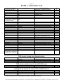
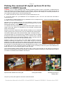
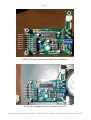
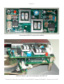
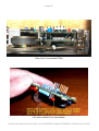
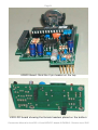
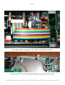
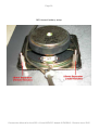
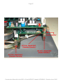
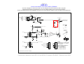
Construction Manual
for the
K2DI v.III, Digital Interface
and
K2DI-PCI, Computer’s Interface
by Paulí Núñez,
EA3BLQ
Revision June, 2005
Page 2
This page is left blank on purpose
Construction Manual for the K2DI v.III and K2DI-PCI boards © EA3BLQ - Revision June 2005
Page 3
INDEX
Foreword ..................................................................... 3
K2DI v.III Digital Interface ............................................ 4
Picking the received AF signal up from P2 at the KAF2 or
KDSP2 boards .............................................................. 9
K2DI-PCI Computer Interface....................................... 10
Pictures and Schematics .............................................. 15
How to install the separators ........................................ 25
Schematics ................................................................ 29
FOREWORD:
This document could be considered as the 4th and last installment of my Digital Interface
Saga. The other three installments or episodes being: “K2 Digital Interface v.I”, “K2 Digital
Interface v.II.2” and “DI v.II.2 installed into the K2/100”.
For those of you who do not know it; let me succinctly explain this part of the story. If you
already know it and think I am being too repetitive, please accept my apologies and thanks
for your bearing with me.
It was back in summer 2002, when Elecraft launched the KAF2 option, -latter on they
launched the KDSP2 as a DSP filter alternative to the KAF2-, when I discovered that my DI
v.II.2, Digital Interface, could not be installed into a Complete Basic K2, featuring all the
options: KDSP2 or KAF2, KAT2, KIO2 and KBT2, nor into the Integrated K2/100, because in
neither of the two set-ups there was any free space available for my PCB. At the time it
could only be installed in a NO KAF2 or NO KBT2 configuration of the K2 as explained in the
K2 Digital Interfacev.II.2 PDF file.
From that moment on I promised myself I had to find a way out of this “cul-de-sac”. It was
a personal defy I had to overcome. From time to time I gave a thought to the challenging
problem and it was by mid November 2003 that I was suddenly struck with new ideas that
gave rise to a new design of my Digital Interface, the K2DI v.III. When I tested the
prototype board, a new idea gave birth to the design of the K2DI-PCI, Computer Interface,
as an optional daughter board of the DI.
The boards are silk-screened and double sided with plated-through holes, as usual.
The main features of both circuits are explained in the forthcoming pages of this document.
Construction Manual for the K2DI v.III and K2DI-PCI boards © EA3BLQ - Revision June 2005
Page 4
K2DI v.III Digital Interface
Main features:
•
The circuit is the very same as the one used in v. II.2 but for an outlet of 5VDC
that has been added to supply voltage to the K2DI-PCI. The board has been
redrawn to a much smaller size: 59 mm (2 5/16") x 35 mm. (1 3/8").
•
Its features include the Microphone Configuration Extender as well as a buffered,
fixed audio output and the cutting of the Front Panel microphone connector's AF
and PTT lines when transmitting data, so as to avoid the unwanted transmission
of shack noise through a live microphone.
•
This board may be used as a stand alone Digital Interface by connecting J3 to a
Mini Din connector at the rear K2 panel, or as a mother board for the K2DI-PCI.
How it works:
Microphone Configuration Header Extender
All pins of J1 and J2 are connected in parallel except for the AF and PTT lines, which are
connected in parallel only while the K2 is in standby or reception mode but are cut while
transmitting digital data, as explained further on.
Through the ribbon cable, J1 receives and sends signals from and to the Microphone
Configuration Header at the Front Panel board and because of the parallel connection of J1
and J2, J2 becomes an extension of the aforementioned Configuration Header. Thus J2 is
the header where you are to configure the Front Panel Mic Connector in accordance with
your microphone’s wiring and needs.
Buffered, fixed audio output:
The received audio is fed to J4 either from Aux Audio J5 at the K2's RF Board or from pins
1 and 2 at P2 on the KAF2 or KDSP2 board.
Although I don't see any inconvenience to feed the AF signal by taping P2 at the KAF2 or
KDSP2, instead of J5 at the RF board, so as to take advantage of the filters, this is the
user's choice. In any case, care must be taken not to tape and connect the wrong pins to
J4 at K2DI board. P2 at the KAF2 and KDSP2 has the GND signal at pin 3, while J4 at K2DI
and J5 at the K2's RF board have the GND signal at pin 2. An error when identifying the
pins would produce a short. To prevent this I have modified the P2 three pins male
header so that when installed, I get the normal 3 pins male header on the bottom side of
the board while I also get a 2 pin male header on the top side (pins 1 and 2). Further on
this document you’ll find pictures showing this mod.
For consistency sake, I decided to copy the Elecraft's original K2 Audio Amplifier circuit to
feed U2, the AF amplifier (LM386N) and to control its audio level. The use of a couple of
J310 FET (Q1 and Q2), biased through a 3.3 MOhm resistor, as in the K2, is very useful as
it allows the disconnection of the AF amplifier from the product detector when on data
transmission.
Construction Manual for the K2DI v.III and K2DI-PCI boards © EA3BLQ - Revision June 2005
Page 5
Cutting the Front Panel mike connector's AF and PTT lines and muting the
AF amplifier, when transmitting data:
Due to its low current drain and its switching features, I've chosen the use of a CD4053BE
CMOS Analogue Multiplexer to cut and commute the AF and PTT lines from the Front Panel
Microphone Connector, through J1, to the Rear Digital Connector when transmitting data,
and to disconnect U2, the audio amplifier LM386, from the product detector by grounding
the gates of Q1 and Q2, following Elecraft's design.
K2DI STANDBY (Receive) POSITION
The K2DI circuit schematic (see page 29) shows the device in its standby (receive)
position, by default, the multiplexer mosfets are biased high due to pins 9, 10 and 11 of
U1, CD4053BE CMOS, being fed with 5V DC through R3 (a 10K resistor). In this way we
have:
a) The ground connected at pin 14 of U1 (a) goes nowhere as pin 13 has no connection.
b) The outgoing microphone signal from the AF pin at J2 goes to the AF pin in J1 through
pins 15 and 1 of U1 (b), as both AF pins are contacted in parallel, and
c) The signal from the PTT pin at J1 goes to the PTT pin at J2 through pins 4 and 3 of U1
(c), connecting the PTT pins in parallel too and thus enabling the Front Panel AF and PTT
lines.
Because of the DC component (2.5 V fed through R1 and R2) present in the U1 (b), three
10 µF electrolytic capacitors (one inlet and two outlets of U1) are needed to decouple the
DC from the signal.
K2DI DIGITAL TRANSMIT POSITION
When, because of data transmission, the PTT is keyed through the Rear Data Connector or
by means of the K2DI-PCI Serial or Tone (VOX) circuits, pins 9, 10 and 11 of U1,
CD4053BE, are grounded through pin 3 at J3. Then the voltage at those pins drops to 0 V.,
setting the multiplexer mosfets low and thus three switching operations are activated:
1) U1 (a) - Switches pin 14 from pin 13 to pin 12 and grounds the gates of Q1 and Q2,
setting them low and thus disconnecting the AF amplifier.
2) U1 (b) - Switches pin 15 from pin 1 to pin 2, connecting the outgoing digital signal
received from the computer’s soundcard through pin 1 of J3, and coming from pin 1 of
the MiniDIN connector or from pin 1 of P1 at the K2DI-PCI board, to the AF pin at J1 and
thus to the K2 TX circuitry. The unwanted mic signal coming from the AF pin at J2 (if
any) is cut and has no way out.
3) U1 (c) - Switches pin 4 from pin 3 to pin 5, keying the rig by grounding the PTT pin at J1
and disconnecting the microphone PTT line at J2
CAUTION:
•
Avoid triggering the K2 PTT through the KI/O2 by means of a program’s CAT
facility. If you do, the K2DI v.III WILL NOT be activated and the Digital
transmission WILL NOT take place.
Construction Manual for the K2DI v.III and K2DI-PCI boards © EA3BLQ - Revision June 2005
Page 6
K2DI v.III Parts List
DESIGNATORS
VALUE
C1, C2, C3, C4, C10
C5
C8
C10
C6
C7, C9
J1
J1 and Microphone.
Configuration Header at
Front Panel board
J2
J4
J5 at the RF board
J4 & J5 at RF board
J4 and J5 at RF board
Q1, Q2
R4
R3
R1, R2
R5
R6
(*)
R7
DESCRIPTION
QTY
10µF 16/25v
220µF 16/25v
.01
.022
.047
.1
Right angle dual row header
IDC Female connector for flat
cable.
Electrolytic or tantalum capacitor
Electrolytic capacitor
Capacitor "103"
Capacitor “223”
Capacitor "473"
Capacitor "104"
16 pin male
FC-16P (16 pin female dual row)
5
1
1
1
1
2
1
2
Dual-row header
Connector with locking tab
Male header
Housing
Hardware
J310
2.7 Ω
10K
100K
3.3 MOhm
2K POT 3329H202 or T7YB
220 Ω
1
1
1
2
6
2
1
1
2
1
1
1
1
U1
U2
J2
Separators
Separator
Separator
Separators
Screws
Screws
Nuts
Washers
J1 at K2DI and Mic.
Configuration Header at
the K2’s Front Panel Brd.
Dig. Interface v.III
CD4053BE or HEF4053BP
LM386N
Hardware
Hardware
Hardware
Hardware
(1)
Hardware
Hardware
Hardware
Hardware
Hardware
Miscellaneous
16 pin male
3 pin male
3 pin male
3 pin female
Female crimp pins for the housings
FET TO-92
Resistor (red-violet-gold)
Resistor (brown-black-orange)
Resistor (brown-black-yellow)
Resistor (orange-orange-green)
Trimmer pot for audio level adjustment
Resistor (red-red-brown)
See text for comments on R7 (*)
CMOS (16 pins)
Low Voltage Audio Amplifier (8 pins)
Mic Conf. Header Extender Jumpers
Male-female hexagonal 1.8cm.
Male-female hexagonal 1.5cm.
Female-female hexagonal 1.5cm.
Male-female hexagonal 7mm
M3 pan head screws 4mm.
M3 pan head screws 6mm.
M3 nuts
Split Lock washer
15.5 cm. flat ribbon cable 16 wires
Miscellaneous
Printed Circuit Board
J3
J3
J3
MiniDIN Connector
Male Connector with locking tab
Housing
Hardware
Miscellaneous
1
1
8
2
1
1
3
4
4
4
4
1
PCB used as a stand alone Digital Interface
4 pin male
4 pin female
Female crimp pins for the housing
4 pin panel MiniDIN connector
1
1
4
1
PCB used as mother board for the K2DI-PCI board
J3
J5
Male header
Male header
4 pin male
2 pin male
1
1
Picking the AF up from P2 at the KAF2 or KDSP2 boards
P2 at KAF2 or KDSP2
P2 at KAF2 or KDSP2
P2 at KAF2 or KDSP2
P2 at KAF2 or KDSP2
(1)
Special Male-male header
Housing
Locking tab
Hardware
3 and 2 pin
2 pin female
2 pin male
Female crimp pins for the housing
1
1
1
2
To be used only in case the KBT2 option is installed. (See pictures section)
Construction Manual for the K2DI v.III and K2DI-PCI boards © EA3BLQ - Revision June 2005
Page 7
ASSEMBLY INSTRUCTIONS:
Please note that all the soldering rules, warnings and tips you have learned and used when
assembling your K2, are to be applied in the assembly of this circuit too.
Install and solder components in the following order:
a) _R1, _R2: 100K resistors (brown-black-yellow)
b) _R3: 10K resistor (brown-black-orange)
c) _R4: 2.7Ω resistor (red-violet-gold)
d) _R5: 3.3 MOhm resistor (orange-orange-green)
e) _R6: 2K trimmer pot (3329H202 or T7YB). By factory default, the trimmer pot is usually
set to its midpoint [+/- 1 Kohm]
Once installed, setting R6 clockwise (CW) will increase the resistance and thus the volume
level of the signal fed to U2 (LM386 audio amplifier). Obviously, to decrease the volume,
R6 is to be set counterclockwise (CCW).
f) _R7: 220Ω resistor (red-red-brown) * See text bellow for notes on this resistor.
g) _C6: 0.047µF (473) capacitor
h) _C7, _C9: 0.1µF (104) capacitors
i) _C8: 0.01µF (103) capacitor
j) _C10: 0.022µF (223) capacitor
k) _Q1, _Q2: J310 FET
l) _J1: Dual row right angle header (16 pin male)
m) _J2: Dual row header (16 pin male)
n) _J3: Connector w/locking tab (4 pin male), if K2DI v.III. is used as a stand alone board.
A 4 pin male header when K2DI is used as a motherboard in conjunction with the K2DI-PCI
o) _J4: Connector w/locking tab (3 pin male)
p) _C1, _C2, _C3, _C4, _C11: 10µF 16/25v electrolytic capacitors
q) _C5: 220µF 16/25v electrolytic capacitor. If the K2DI-PCI board is to be installed, please
bend the leads so that the capacitor is installed resting on its side on the PCB.
r) _U1: CD4053BE or HEF4053BP CMOS (16 pins)
s) _U2: LM386 low voltage audio amplifier (8pins)
Construction Manual for the K2DI v.III and K2DI-PCI boards © EA3BLQ - Revision June 2005
Page 8
(*) NOTES ON THE R7 RESISTOR'S VALUE TO CONTROL LM386's GAIN.
The manufacturer's General Description of the LM386 reads: "…The gain is internally set to
20 to keep external part count low, but the addition of an external resistor and a capacitor
between pins 1 and 8 will increase the gain to any value up to 200."
The factory default gain of ±20, attained through the inner 1.35Kohm resistor allocated
between pins 1 and 8 is too low for our needs.
On the other way if we externally bypass that resistor by inserting a 10µF electrolytic
capacitor between those pins (+ lead to pin 1) the gain is increased to 200. Good enough
to drive a 4Ω speaker but too high for the sound card, as it gets overdriven.
On this account and by inserting one external resistor in parallel with the inner resistor and
in series with the electrolytic capacitor, between pin 8 of the IC and the (-) lead of the
capacitor, we may set that gain to the level that meets with our needs, within the range of
20-200.
As a result of some computing, I've got the following options for R7's resistor value:
1) One 1.2Kohm resistor (brown-red-red) will render a gain of about 50 (perhaps a bit on
the low side)
2) One 330Ω resistor (orange-orange-brown) will render a gain of about 75
3) One 220Ω resistor (red-red-brown) will render a gain of about 90.
4) One 180Ω resistor (brown-grey-brown) will render a gain of about 100 and
5) One 100Ω resistor (brown-black-brown) will render a gain of about 125
I have chosen option #3, but the builder may choose the option he/she thinks most
suitable for his/her needs and/or preferences.
CAUTION:
•
Please, remember to configure J2 header (the microphone configuration header
extender) in accordance with your mic needs, as per Table 2 on the Elecraft’s
“Assembly and Operating Instructions” for the KSB2 SSB Adapter: “P1 Wiring for
Selected Microphones”, as you would do on the Microphone Configuration Header
at the Front Panel board itself.
•
If your intention is to construct the K2DI-PCI board too, then it is most
convenient to set up the mic configuration at this step, before constructing and
assembling the K2DI-PCI daughter board to the K2DI v.III board. If you fail to do
so you may forget this step and be compelled to undo the K2DI v.III / K2DI-PCI
assemblage so that you can reach the J2 header at the K2DI.
Construction Manual for the K2DI v.III and K2DI-PCI boards © EA3BLQ - Revision June 2005
Page 9
Picking the received AF signal up from P2 at the
KAF2 or KDSP2 boards
Caution: If you, to take advantage of the filtering provided by either circuitry of the KAF2 or KDSP2 devices
and/or because the connection for the K2DI v III.2 is handier, decide to pick the received AF signal up from the P2
connection at the KAF2 or KDSP2 boards, instead of picking it up from the auxiliary AF connection provided at J5
on the RF board, please bear in mind the following facts:
a.- In both cases the K2’s audio circuit is the very same balanced one, but
b.- On the RF board, the 3 pin distribution at J5 correspond to pins 1 and 3 for the audio lines and GND is
connected to pin 2.
c.- On the KAF2 or KDSP2 boards, the 3 pin distribution at P2 correspond to pins 1 and 2 for the audio lines while
the GND connection is located at pin 3.
Obviously the 3 pin female connector you may prepare to connect J4 at the
K2DI to J5 on the RF board cannot be used for connection to P2 on the
KAF2/KDSP2 boards. It would produce a short.
To avoid this risk I have prepared the special male-male header shown on the
image at the right, which is to substitute the one provided by Elecraft with
either of their devices.
Should you have the original P2 header already installed you are to desolder
it taking outmost care in the process so as not to damage the soldering pads.
The square soldering pad, near the down board’s edge, corresponds to pin 1.
The special header is to be introduced for installation into the KAF2 or KDSP2
through the bottom side of the board, taking care to position its pin 1 through
the square soldering pad. Check before soldering. The 3 equal pins with the
plastic holder go on the bottom side. (See pictures below)
Soldering is done on the top side of the board. Before soldering check the
header’s positioning once again and, if it is ok, solder only pin 3. Check the
positioning once again and see that the plastic holder is flush with the board
and that the pins are perpendicular to the board and parallel to those of P1. If
any correction is necessary please do so by reheating the pin 3 solder. If it is ok please go on soldering pins 1 and
2, but taking care to use a minimum amount of solder, just the necessary to secure a good contact between the
board and the pin. Use a magnifying glass to check the joints.
Once finished soldering please prepare the locking tab by cutting out the borders of the indents at its bottom to
allow more contact field for the pins and perhaps you will have to shorten its base by a couple millimeters to allow it
to sit flush on the board when installed in the two pins.
Special header installed w/o locking tab.
Locking tab installed.
Showing tab and pin 3
(GND) solder.
This pick up set-up also applies for the KAF2 audio filter board.
Construction Manual for the K2DI v.III and K2DI-PCI boards © EA3BLQ - Revision June 2005
Page 10
K2DI-PCI Computer Interface
Main features:
•
The board measures 73 mm (2 7/8") x 35 mm (1 3/8").
•
Its circuitry (see the schematics on page 29) features a Serial Port (RTS and DTR)
PTT or a VOX (Tone) PTT, to be chosen by the user when setting the J3 and J4
jumpers in accordance with his/her needs and/or preferences.
•
The Serial Port is isolated by an optocoupler.
•
The Line In/Mic or Line Out/Spkr soundcard connection is isolated by two
600:600Ω coupling transformers (Atech ATS-075), which feature a very flat
response and an Insertion Loss of 1.0 dB Max at 1 Khz 1 Vrms.
•
One 10K POT controls the AF In audio volume level.
•
A connection for an optional PTT ON Led is provided, to be installed in case this
board is used as an external stand alone computer interface.
•
This board has been designed to be the K2DI's daughterboard but, as I have
pointed out, it also can be used as a stand alone external Computer's interface.
How it works:
PTT SWITCHING
The PTT circuit provides the possibility of using any of two modes of PTT switching: either
Serial (RS232) PTT or VOX (Tone) PTT, depending on the user’s choice or needs.
Many a program for digital communications (PSK31, SSTV, etc.), when setting-up the PTT
switching option, allows the user to choose either Serial COM port or Soundcard/VOX and,
when choosing the former, you can even choose the use of the RTS, DTR or both RTS &
DTR signals.
Serial (RS232) PTT
This mode features the use of an Optically Coupled Isolator, the 4N32, to achieve the
switching of the PTT while maintaining a very good isolation between the rig and the
computer. This Optocoupler (U1 on the schematic) is driven when any or both pins RTS
and/or DTR of a Computer’s Serial (RS232) connector (pins 4 and 7 on a DB9 and pins 4
and 20 on a DB25) are biased high (±5 vDC). When this happens the 4N32’s inner infrared
LED (pin 1 anode and pin 2 cathode) biases the photo sensor base so that the collector (pin
5) and the emitter (pin 4) become conductive and grounds the PTT line on pin 3 at P1, thus
switching the PTT circuit on.
Pins 1 and 2 at J4 must be jumpered. J3 must be open.
VOX (Tone) PTT
This circuit uses a Low Power Dual J-FET Operational Amplifier, the TL062 (U2 on the
schematic), and consists of two sections with different functionality:
In the first section (U2 a) a square wave signal is obtained from the AF signal coming from
the TR1 secondary and fed to pin 2. When the tension level on pin 2 is higher that that on
pin 3, the output on pin 1 will be at 0 (zero) volts level, and vice versa, when the tension
level on pin 2 is lower than that on pin 3, the output level on pin 1 will be that of ±5 vDC.
Construction Manual for the K2DI v.III and K2DI-PCI boards © EA3BLQ - Revision June 2005
Page 11
In this way pin 1 will render a square wave signal whenever there is an AF signal fed to pin
2. In the absence of such an AF signal the output will be 0 (zero) volts.
Because of this, whenever there is an AF signal fed to pin 2, the 1N4148 (D3) diode
rectifies the square wave signal present at pin 1 and charges the C5 capacitor at 5 vDC.
The values of the conjunct R7 and C5 determine the time constant, when the capacitor will
remain charged.
While C5 is charged, the second section (U2 b) will render 5 vDC on its outlet at pin 7.
When, because there is no AF signal at pin 2, C5 gets discharged, there will be 0 (zero)
volts present at pin 7.
The tension present at pin 7, through R5 biases Q1 which emitter and collector become
conductive and drive the PTT switch by grounding pin 3 at P1.
Pins 2 and 3 at J4 as well as those of J3 must be jumpered.
Soundcard isolation
The soundcard’s Line In/Mic and Line Out/Spk are isolated from the circuit by a couple of
600:600 Ω audio coupling transformers by Atech Technology Co. Ltd., the ATS-075, which
offers a very flat response and a very low profile.
AF In level
So as not to overdrive the transmitter and to prevent IMD, the level of the audio fed to the
K2 for transmission may be set by means of the 10K trimmer potentiometer R2.
CAUTION:
•
If and when using the VOX (Tone) PTT option, care must be taken to mute, at
your OS, all the sounds and chimes scheduled to announce Windows’ and other
program’s events or happenings (Start -> Configuration -> Control Panel ->
Sound, Audio and Voice Devices -> Change Sound Scheme -> Properties ->
Sound). It is MOST IMPORTANT that no unwanted sound is produced. Otherwise,
those sounds will inadvertently trigger the PTT and, to our own despair and
annoyance or what is more embarrassing, to that of the contacted remote station
or the listeners, the unwanted sound will be transmitted.
•
If your Sound Card has the full duplex feature, when setting the Sound Card
Mixer, remember to mute the Line In or Microphone In at the Sound Level
Control, so that the received audio or noise is not echoed to the Line Out outlet
and thus get the PTT switched On continuously.
Construction Manual for the K2DI v.III and K2DI-PCI boards © EA3BLQ - Revision June 2005
Page 12
K2DI-PCI Parts List
DESIGNATORS
VALUE
DESCRIPTION
QTY
C1
C5
C3, C4
C2
D1, D2, D3
J1
J1b
J2
J2b
J3
J4
LED1
P1
P2
Q1
R1, R3
R5
R2
R4, R7
R6
R8
TR1,TR2
U1
U2
J1b & J2b
J3, J4
Separators
.1µF
.47µF
4.7µF
10µF
1N4148
Connector with locking tab
Housing
Connector with locking tab
Housing
Male header
Male header
LED
Female Header
Female Header
PN2222A or MPS2222A
470 Ohm
10K
10K POT (Miniature)
100K
3.3M
1K
Transformer
4N32
TL062
Hardware
Hardware
Hardware
1
1
2
1
3
1
1
1
1
1
1
1
1
1
1
2
1
1
2
1
1
2
1
1
7
2
3
Lock Washers
MiniDin Conn.
MiniDin Conn.
K2DI-PCI
Hardware
Hardware
Hardware
Miscellaneous
Capacitor "104"
Capacitor "474"
Electrolytic or tantalum capacitor
Electrolytic or tantalum capacitor
High speed diode
3 pin male
3 pin female
4 pin male
4 pin female
2 pin male (PTT jumper)
3 pin male (PTT jumper)
red LED
4 pin female
2 pin female
NPN General purpose transistor
Resistor (yellow-violet-brown)
Resistor (brown-black-orange)
Trimmer pot for audio level adjustment
Resistor (brown-black-yellow)
Resistor (orange-orange-green)
Resistor (brown-black-red)
Coupling transformer Atech ATS-079B
Optocoupler
Dual operational amplifier
Female crimp pins for the housings
PTT Jumpers
Female-female hexagonal 1cm.
separators
Split Lock Washers
4 pin Chassis MT MiniDin to Sound Card
3 pin Chassis MT Mini Din to RS232
Printed Circuit Board
3
1
1
1
MOUSER
652-3329H-1-103
421-ATS079B
161.2104
161,2103
Construction Manual for the K2DI v.III and K2DI-PCI boards © EA3BLQ - Revision June 2005
Page 13
ASSEMBLY INSTRUCTIONS:
Please note that all the soldering rules, warnings and tips you have learned and used when
assembling your K2, are to be applied in the assembly of this circuit too.
Install and solder components in the following order:
a) _R1 _R3: 470 Ω resistors (yellow-violet-brown)
b) _R8: 1K resistor (brown-black-red)
c) _R5: 10K resistor (brown-black-orange)
d) _R4, _R7: 100K resistors (brown-black-yellow)
e) _R6: 3M3 resistor (orange-orange-green)
f) _D1, _D2, _D3: 1N4148 High speed diode
g) _C1: .1µF capacitor (104)
h) _C5: .47µF capacitor (474)
i) _C3, _C4: 4.7µF electrolytic or tantalum capacitor
j) _C2: 10µF electrolytic or tantalum capacitor
k) _P1: 4 pin female header (to be installed on the bottom side of the board and
soldered on the top) (*)
l) _P2: 2 pin female header (to be installed on the bottom side of the board and
soldered on the top) (*)
m) _R2: 10K POT trimmer
n) _Q1: NPN General purpose transistor (PN2222A)
o) _U1: Optocoupler (4N32)
p) _U2: Dual operational amplifier (TL062)
q) _LED1: Optional PTT on LED (red). Useful if the board is installed as a stand alone
External Computer Interface.
r) _TR1, _TR2: 600:600Ω Coupling transformer (Atech ATS-075). Mouser’s catalogue
part # 421-ATS075 (page 542)
s) _J1: Connector with locking tab (3 pin male)
t) _J2: Connector with locking tab (4 pin male)
u) _J3: Header (2 pin male)
v) _J4: Header (3 pin male)
(*) Should the board be used as a stand alone External Computer Interface, these two
female headers ought to be substituted by a 4 and 2pin male connectors installed on the
top face of the board and soldered on the bottom.
Construction Manual for the K2DI v.III and K2DI-PCI boards © EA3BLQ - Revision June 2005
Page 14
This page is left blank on purpose
Construction Manual for the K2DI v.III and K2DI-PCI boards © EA3BLQ - Revision June 2005
Page 15
Pictures
Construction Manual for the K2DI v.III and K2DI-PCI boards © EA3BLQ - Revision June 2005
Page 16
K2DI v.III XRay image
K2DI V.III Parts Placement
Construction Manual for the K2DI v.III and K2DI-PCI boards © EA3BLQ - Revision June 2005
Page 17
K2DI V.III Constructed and ready to be installed
K2DI v.III installed on the top cover of the K2
Construction Manual for the K2DI v.III and K2DI-PCI boards © EA3BLQ - Revision June 2005
Page 18
K2DI-PCI PCB’s x-ray image
K2DI-PCI Parts Placement
Construction Manual for the K2DI v.III and K2DI-PCI boards © EA3BLQ - Revision June 2005
Page 19
Constructed K2DI-PCI ready to be installed
K2DI-PCI fitted on top of its motherboard, the K2DI v.III
Construction Manual for the K2DI v.III and K2DI-PCI boards © EA3BLQ - Revision June 2005
Page 20
Side view of the installed PCBs
KF2 with modified 3 pin male header
Construction Manual for the K2DI v.III and K2DI-PCI boards © EA3BLQ - Revision June 2005
Page 21
KDSP2 Board. Mind the 2 pin header on the top
K2DI-PCI board showing the female headers placed on the bottom
Construction Manual for the K2DI v.III and K2DI-PCI boards © EA3BLQ - Revision June 2005
Page 22
Ribbon cable connected to the Front Panel Mic Configuration Header
Side view of the K2, showing the ribbon cable coming out between the Control and
Front Panel boards, the KDSP2 option and the installed K2DI v.III & K2DI-PCI
boards. Mind the J1 and J2 straight connectors at the K2DI-PCI board. Right angled
connectors collided with the Side Panel.
Construction Manual for the K2DI v.III and K2DI-PCI boards © EA3BLQ - Revision June 2005
Page 23
The ribbon cable connected to the K2DI v.III Digital Interface
How the Serial PTT and Soundcard cables are fixed to the top cover
Construction Manual for the K2DI v.III and K2DI-PCI boards © EA3BLQ - Revision June 2005
Page 24
I have used a Minijack stereo for the Serial PTT rear connection and have isolated
the PC signal GND with one bakelite washer. The jack is centered in the former OUT
XVTR hole.
Construction Manual for the K2DI v.III and K2DI-PCI boards © EA3BLQ - Revision June 2005
Page 25
How to install the separators
The separators as well as the screws and nuts I provide are Metric 3 and because of
that and for esthetic consistency sake, I suggest that, when installing the board(s)
on the top cover of the K2, the constructor uses them instead of using the
hardware supplied by Elecraft (screws and bolts for the loudspeaker and malefemale separators for the KBT2)
KBT2 Internal battery setup
Substitute the screws, bolts and KBT2 Battery Bracket’s separators for the ones
supplied with the K2DI v.III kit.
Construction Manual for the K2DI v.III and K2DI-PCI boards © EA3BLQ - Revision June 2005
Page 26
NO Internal battery setup
Construction Manual for the K2DI v.III and K2DI-PCI boards © EA3BLQ - Revision June 2005
Page 27
Construction Manual for the K2DI v.III and K2DI-PCI boards © EA3BLQ - Revision June 2005
Page 28
This page is left blank on purpose
Construction Manual for the K2DI v.III and K2DI-PCI boards © EA3BLQ - Revision June 2005
Page 29
SCHEMATICS
Construction Manual for the K2DI v.III and K2DI-PCI boards © EA3BLQ - Revision June 2005
Page 30
K2DI v. III
K2 Digital Interface featuring a Mic. Configuration Header Extender and Rear Panel Data Connector
(It Includes a buffered, fixed audio output and the cutting of Front Panel mic. connector's AF and PTT lines, when transmitting data).
© Paulí Núñez, EA3BLQ - November 2003
J3 to
MiniDIN conn.
or to P1 at the
K2DI-PCI
9
16
U1 (c)
1
AF
C1
10 µF
3
4
AF
2
DN
3
UP
4
FUNC
5
10
U1 (b)
+
5
PTT
R2
100K
CD4053BE
PTT
R1
100K 15
1
C2
10 µF
+
2
C3
10 µF
+
1
CD4053BE
6 7 8
2
MiniDIN connector
(connections as seen from
K2's rear panel)
3
R3
10K
+5VDC (10mA max.)
+5V
6
GND
7
J5 to P2 at
K2DI-PCI
+
AF IN
GND
PTT
AF OUT
NC
NC
4
C4
10 µF
+
C5
220 µF
J310
8
GND
11
J1 to FP Board
Mic. Config. Header
123456-
13
NC
J2 Extended
Mic. Config. Header
R4
2.7 Ω
U1 (a)
CD4053BE
1
R5
3.3M
2
+
2
C8
0.01
C10
0.022
3
S
D
CW
8
5
7
4
C9
0.1
CCW
J4 to RF Board, J5
U2
LM386N
Q2
J310
3
R7*
220 Ω
6
1
G
G
G
C11
10 µF
C7
0.1
D
Q1
J310
S
C6
0.047
12
S
D
14
NC
R6
2K trimmer
pot.
Notes: All resistors are 1/4 watt and their value is
in ohms; K = 1,000 and M = 1,000,000
Decimal values of capacitance are in
microfarads (µF)
NC = No connection
See text for comments on R7*
Construction Manual for the K2DI v.III and K2DI-PCI boards © EA3BLQ - Revision June 2005
Page 31
K2DI-PCI
Sound card interface for the K2's K2DI by EA3BLQ
Circuit for a daughter PC board of the K2DI v.III PCB, designed to interface the K2's DI with a computer.
It features Opto isolation for the RS232 PTT circuit, as well as isolation for the sound card connections.
Another remarkable feature is the possibility to choose the PTT mode between RS232 or VOX, according to user preferences.
D1
1N4148
R1
470 Ω
J1
RS-232
DB 9
1
6
2
7
3
8
4
9
5
4 - RTS
7 - DTR
5 - GND
1
2
D2
1N4148
U1
1
6
2
5
NC
J4
PTT mode Jumper
3
3
4N27
4N32
4
NC
1
} Serial PTT (Do NOT jump J3)
To P1 PTT Line (pin 3)
} Tone PTT (J3 MUST be jumped)
3
R4
470 Ω
5 VDC
R3
500 Ω
To P1 AF In (pin 1)
R2
10K
C3
4.7µF
TR1
5 VDC
5 VDC
J3
2
-U2 (a)
J2 Pin 2
Tone PTT
Jumper
C2
10µF
+
R8
100K
+
Digital PTT On
LED
(Optional)
R9
1K
1
TL062
3
+
C1
.1µF
8
5
D3
1N4148
4
R7
3M3
C5
,47 µF
6
+
-
U2 (b)
TL062
7
R6
10K
B
Q1
PN2222A
BC546
J2 Pin 1
Atech ATS-075
600:600
+
C4
4.7µF
C
E
5 VDC
P2
R5
100K
PC GND
+
TR2
J2
P1
To P1 AF Out (pin 4)
J2 Pin 3
J2 Pin 4
Atech ATS-075
600:600
PC GND
SCard's GND
1
AF In
1
SCard's Spkr/Line Out
2
GND
2
SCard's Mic/Line In
3
PTT
3
SCard's GND
4
AF Out
4
Notes:
All resistors are 1/4 watt and their
value is in ohms; K = 1.000 and
M = 1.000.000
Decimal values of capacitance
are in microfarads ( µF).
NC = No connection.
P1 connects to K2DI J3
P2 connects to K2DI J5
© November 2003 by Paulí Núñez, EA3BLQ
Construction Manual for the K2DI v.III and K2DI-PCI boards © EA3BLQ - Revision June 2005
Page 32
Construction Manual for the K2DI v.III and K2DI-PCI boards © EA3BLQ - Revision June 2005