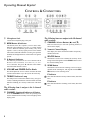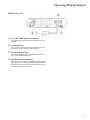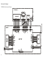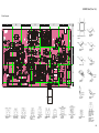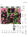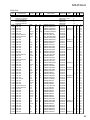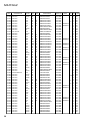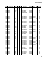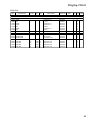
1
VERTEX STANDARD CO., LTD. 4-8-8 Nakameguro, Meguro-Ku, Tokyo 153-8644, Japan VERTEX STANDARD VHF Land Mobile Transceiver US Headquarters 10900 Walker Street, Cypress, CA 90630, U.S.A. International Division 8350 N.W. 52nd Terrace, Suite 201, Miami, FL 33166, U.S.A. VX-2000V YAESU EUROPE B.V. P.O. Box 75525, 1118 ZN Schiphol, The Netherlands Service Manual ©2003 VERTEX STANDARD CO., LTD. YAESU UK LTD. Unit 12, Sun Valley Business Park, Winnall Close Winchester, Hampshire, SO23 0LB, U.K. VERTEX STANDARD HK LTD. E095390A 40 channel version Unit 5, 20/F., Seaview Centre, 139-141 Hoi Bun Road, Kwun Tong, Kowloon, Hong Kong 4 channel version Introduction This manual provides technical information necessary for servicing the VX-2000V VHF Land Mobile transceiver. The VX-2000V is carefully designed to allow the knowledgeable operator to make nearly all adjustments required for various station conditions, modes and operator preferences simply from the controls on the panels, without opening the case of the transceiver. The VX-2000V Operating Manual describes these adjustments, plus certain internal settings. Servicing this equipment requires expertise in handling surface mount chip components. Attempts by non-qualified persons to service this equipment may result in permanent damage not covered by warranty. For the major circuit boards, each side of the board is identified by the type of the majority of components installed on that side. In most cases one side has only chip components, and the other has either a mixture of both chip and lead components (trimmers, coils, electrolytic capacitors, packaged ICs, etc.), or lead components only. While we believe the technical information in this manual is correct, Vertex Standard assumes no liability for damage that may occur as a result of typographical or other errors that may be present. Your cooperation in pointing out any inconsistencies in the technical information would be appreciated. Vertex Standard reserves the right to make changes in this transceiver and the alignment procedures, in the interest of technological improvement, without notification of the owners. Contents Operating Manual Reprint ............................ 2 Specifications ................................................... 7 Exploded View & Miscellaneous Parts....... 8 Block Diagram ................................................. 9 Interconnection Diagram............................. 13 Circuit Description ...................................... 15 Alignment....................................................... 19 Board Unit (Schematics, Layouts & Parts) MAIN Unit ............................................................... 23 DISPLAY-1 Unit ...................................................... 49 DISPLAY-2 Unit ...................................................... 53 VR Unit ..................................................................... 57 MIC Unit .................................................................. 58 1 Operating Manual Reprint CONTROLS & CONNECTORS 4 channel version À Microphone Jack Connect the microphone plug to this jack. Á MONI Button & Indicator This button selects the “squelch” (receiver mute) mode. When the yellow indicator is off, “tone” or “coded” squelch is active. When the indicator glows steadily, only “noise squelch” is active, and any signal present on the channel will be heard. When the indicator is blinking, the squelch is disabled, and background noise will be heard if no signal is present. 40 channel version The following items are unique to the 40-channel radio versions: Æ CHANNEL Selector Buttons (p) and (q) Push one of these keys to select the operating channel, as shown on the display. Ç Numeric Channel Display This display area shows the channel number and prioritychannel/scan status. È SEL/PRI Button  A Button & Indicator This button is provided for an ACCESSORY function such as HIGH/LOW P OWER selection, “T ALK-AROUND”, or “C ALL ALERT” functions. The green “A” indicator will be illuminated when this function is active. This button is used to select a channel for “Priority” monitoring, and is used together with the SCAN button to select the desired scanning mode. É SCAN Button This button is used to activate scanning, to select or remove channels on the scanning list, and (together with the SEL/ PRI button) to select scanning mode. à VOLUME and POWER ON/OFF Knob This knob adjusts the receiver volume, and turns the radio off when turned all the way to the left into the click-stop. Ä TX/BUSY Indicator Lamp This lamp blinks red when the channel is busy, and glows steadily red during transmission. Do not transmit when this indicator is blinking, as a courtesy to other users of the channel. The following item is unique to the 4-channel radio versions: Å CHANNEL Numbered Indicators & Button Press the CHANNEL button to select the operating channel; the channel number currently in use will light up on the display panel. 2 P Indicator 11 This small dot indicates Priority Channel status (described later). E Indicator 12 This small dot indicates Scanning on/off status (described later). Operating Manual Reprint REAR (Heatsink) À 13.6V DC Cable Pigtail w/Connector The supplied DC power cable must be affixed to this 2-pin connector. Á Antenna Socket The 50-ohm coaxial feedline to the antenna must be connected here, using a “UHF” type (PL-259) plug.  External Speaker Jack An external loudspeaker may be connected to this 2-contact, 3.5-mm miniature phone jack. à DSUB 9-Pin Data Connector External Transmit Audio input, PTT (Push To Talk), Squelch, and Receive Audio output signals may be obtained from this connector for use with accessories such as a data transmission/reception modem, etc. 3 Operating Manual Reprint OPERATION Power ON/OFF Scanning Turn the VOLUME/POWER knob clockwise to turn on the radio. The active display and channel indicators will become illuminated, indicating the status of the radio. The channel indicated will be the same one on which you were operating when the radio was last turned off. To activate scanning on your radio, first place the microphone in its hanger. Now press the SCAN button momentarily. The radio will scan in one of four available Scan Modes (detailed below), and will halt when a signal is received which contains the correct code to open your squelch. Scanning will resume automatically either after a preset interval of a few seconds, or after the other station stops transmitting (depending on how your radio was programmed). Setting the Channel In 4-channel versions, press the CHANNEL button to change channels. In 40-channel versions, the display will show either a channel number or a Scan Mode indicator (Sc, Ur, SP or UP). If a Scan Mode indicator is displayed, press the SCAN button momentarily so that a channel number is displayed; then press either the UP (p) or DOWN (q) button to change channels. Setting the Volume Rotate the VOLUME/POWER knob clockwise to increase the volume level. If no signal is present on which to adjust the volume level, push and hold in the MONI button for two seconds; the yellow “MONI” indicator will blink, and either background noise or a voice signal will be heard. You may now adjust the VOLUME/POWER knob for a comfortable listening level. When you are done, press the MONI button momentarily to return to silent monitoring. Transmitting To transmit, wait until the “TX/BUSY” indicator is off (this indicates that the channel is not in use). Then press the PTT (PushTo-Talk) switch on the side of the microphone; while holding in the PTT switch, speak in a normal voice level across the face of the microphone. During transmission, the red “TX/BUSY” indicator will glow steadily. When you are done transmitting, release the PTT switch; the VX-2000 will revert to the “receive” mode. The remaining instructions apply to 40-channel transceiver versions only Special Transmitter Functions If your VX-2000 is programmed for Busy Channel LockOut, the transmitter will not activate when the PTT switch is pressed unless the “TX/BUSY” indicator is off (so as to prevent interference to other users of the same channel). If the selected channel has been programmed for Automatic Time-Out, you must limit the length of your transmissions. While transmitting with this feature activated, a “beep” will sound ten seconds before the timer expires, and then another “beep” sound as the timer expires: the “TX/BUSY” indicator will shut off, and transmission will cease. Release the PTT switch, listen for a moment, then press PTT again to resume transmission. This feature prevents interference to other users caused by a microphone which accidentally is stuck in the “transmit” position (wedged between seats of a car, etc.). 4 The four Scan Modes, and their corresponding displays, are: Display Sc Ur SP UP Scanning function Scan all channels Scan only user-selected channels Monitor one channel plus dealer-designated Priority Channel(s) Scan user-selected channels plus uer-designated Priority Channel(s) The user-selected channels for the Ur and UP Scan Modes are ones you can set up yourself, as described at the right. The “Priority” channels are those on which signals will take priority over signals received on other channels; that is, if a signal appears on a Priority Channel while another appears on a nonpriority channel, the Priority Channel signal will be heard, and not the other. Up to two of the installed channels may be designated by your Dealer as pre-programmed Priority Channels for the SP mode (the radio will not indicate which they are), and you can additionally program any two channels as “User Priorities” for the UP mode. In the SP mode, the non-priority channel will be the last one displayed. When a Scan Mode is displayed, you can select another by pressing the SEL/PRI button repeatedly (the display will cycle through the above selections). Note that the radio will not scan if the microphone is not in its hanger. Operating Manual Reprint USER PROGRAMMABLE CHANNEL SELECTIONS You can program a list of channels to be scanned, and up to two channels to be monitored on a “priority” basis. Your selections will be maintained in memory until you change or delete them. Setting of these channels involves two small “Dot” indicators at the top of the channel display field. The Dot to the left of the first digit is the “P” (Priority) indicator, while the Dot to the left of the second digit is the “E” (Enable for Scanning) indicator. To create or modify the Scan and Priority selections, first turn the radio off. Now press and hold in the SCAN button while you turn the transceiver back on; continue to hold the SCAN button in for two seconds after the radio has come on, then you may release it. Now press the UP (p) or DOWN (q) button repeatedly, and note whether or not the “E” (right dot) or “P” (left) dots appear on any of your channels. If a dot appears by any channel, it means that it has been designated as either a Scan-Enabled or Priority channel, respectively. To enable or disable a channel from the User Scan list, press the SEL/PRI button momentarily. The “E” dot will appear or disappear, as appropriate. To change the Priority Channels, first cancel both by selecting either, and then pressing the SEL/PRI button momentarily. Now select the channel you wish to designate as the 1st Priority Chan- nel, and hold in the SEL/PRI button for 2 seconds, until a beep sounds and the “P” indicator blinks. If you wish to designate a 2nd Priority Channel, move to that channel, and again hold in the SEL/PRI button for 2 seconds; this time, the “P” indicator will glow, but will not blink. If you have deleted a channel from Priority status, you must reenable it for scanning if you want it to be included on your Scan List. Press the SEL/PRI button momentarily to do this. Coded Squelch - the MONI Button Your transceiver may be programmed so that when the microphone is removed from its hanger, coded squelch is defeated, and you can hear any signal on the channel (the yellow “MONI” indicator will be lit). You can get the same result, without lifting the microphone, by pressing the MONI button momentarily. To avoid listening to unnecessary chatter, keep the microphone in its hanger, and press the MONI button when necessary to turn the yellow indicator off (unless you want to listen to other calls on the channel). Holding the MONI button in for two seconds defeats both the coded squelch and noise squelch, so background noise can be heard (the “MONI” indicator will blink in this case). Press the MONI button momentarily to return the yellow indicator to its previous state (either off or steadily on). OPTIONAL ACCESSORIES CE-20 VPL-1 T9101411 FP-1025A MD-11A8J MH-600D MLS-100 LF-1 VTM-20 F2D-4A/B FTE-18 Programming Software (for IBM PC/compatibles only) Programming Cable Radio-to-Radio Cloning Connection Cable Heavy-Duty (20A) AC Power Supply Desktop Microphone DTMF Back-lit Microphone w/Autodial External Loudspeaker DC Line Filter VX-Trunk II Trunking Mobile Logic Board 2-Tone Decoder Unit ANI Unit 5 Operating Manual Reprint J1003 DSUB 9-Pin Data Connector Pin Assignment Ä Ã Â Á À È Ç Æ Å À SQ: Squelch Signal Output Carrier In: Active High (5 V / 47 kΩ) Á RX_AUD_OUT: Received Audio Output (Two choices available) Á-1 De-Empasized Audio Output: 100 mV / 10 kΩ This output level's default state is fixed at the factory by having no jumper at JP1003 and soldering the jumper at JP1002 on the MAIN Unit. Á-2 Flat / Unmuted Audio Output: 250 mV / 10 kΩ (Unsolder the jumper at JP1002 and solder a jumper at JP1003 on the MAIN Unit to activate Á-2)  EXT_MIC: External MIC Audio Input (Two choices available) Â-1 Pre-Emphasized / IDC / Splatter Filtered Audio Input: 2.5 mV / 600 Ω This input is fixed at the factory by attaching capacitor C1254 across JP1005 and soldering a jumper at JP1004 on the MAIN Unit. Â-2 Flat (Non-Pre-Emphasized) Audio Input: 650 mV / 10 kΩ (Remove the jumper at JP1004 and solder a jumper across JP1005 on the MAIN Unit to activate Â-2) 6 à Not Used Ä GND: Ground Å A_OUTPUT: Accessory Output (Two choices available) Å-1 Not Used This is the default setting at the factory (no jumper across JP1001 on the MAIN Unit). Å-2 Accessory Output: Open Collector Output "A" Lamp ON: Low, "A" Lamp OFF: Open Maximum voltage: 13.8 V, Maximum sink current 5 mA (Solder a jumper at JP1001 on the MAIN Unit to activate Å-2) Æ PTT: External PTT Signal input GND: TX, Open: RX Ç5V Switched and regulated DC 5 V output for supplying power to an accessory. Maximum output current is 50 mA. È Not Used Specifications General Frequency Range (version): No. of Channels & Spacing: Modes of Emission: Frequency Stability: Antenna Requirements: Voltage Requirements: Current Consumption (approx.): Operating Temperature Range: Size (WHD, approx.): Weight (approx.): 134 ~160 or 148 ~ 174 MHz (VHF vers. A/C, respectively) 4 or 40 channels 25-kHz, 12.5-kHz spacing 16K0F3E ,11K0F3E ±0.00025% 50 ohms, unbalanced (SO-239 socket) 11.8 V to 15.6 V DC, negative ground 250 mA Stby, 200 mA Rx, 6.5 A Tx -30 °C to +60 °C (-22 °F to +140 °F) 160 × 40 × 105 mm (6¼ × 1½ × 4¼ inches) 0.85 kg (1.9 lbs.) Receiver Receiver Circuit Type: Intermediate Frequencies: Sensitivity: Double-Conversion Superheterodyne 17.7 MHz , and 450 kHz (all models) 0.2/0.25 µV for 12-dB SINAD 0.3/0.35 µV for 20 dB NQ Hum & Noise Ratio: Better than 45 dB for 25-kHz/step, Better than 40 dB for 12.5-kHz/step Adjacent Channel Selectivity: >70 dB for 25-kHz/step, >60 dB for 12.5-kHz/step Intermodulation Distortion: Better than 65 dB Spurious Rejection: Better than 65 dB External Audio Output Power: 5 watts into 4 ohms with <10% THD Transmitter Power Output: 25/5 watts (high/low, programmable) Modulation Type/Deviation: Hum & Noise Ratio: Frequency Modulation, ±5 kHz (±2.5 kHz ) Better than 45 dB for 25-kHz/step, Better than 40 dB for 12.5-kHz/step Less than 5% Better than 65 dB (below carrier) 600 ohms Modulation Distortion: Spurious Emissions: Microphone Impedance: Specifications are subject to change without notice or obligation. 7 Exploded View & Miscellaneous Parts REF. À Á Â Ã Ä Å Æ VXSTD P/N U24208001 U20208001 U20306002 U23205001 U23206001 U24306002 U31206007 U24308001 Description TAPTITE SCREW M2.6X8 (Lot. 1~5) BINDING HEAD SCREW M2.6X8 (Lot. 6~) BINDING HEAD SCREW M3X6NI TAPTITE SCREW M2.6X5 TAPTITE SCREW M2.6X6 TAPTITE SCREW M3X6NI OVAL HEAD SCREW M2.6X6B TAPTITE SCREW M3X8 Qty. 1 1 4 4 3 5 7 1 VXSTD P/N Q0000062 Description FUSE 10A T9021810 DC CABLE Qty. 2 1 T9206675 WIRE ASSY RA0060100 CASE P1090654 CONNECTOR DISPLAY-1 Unit Å RA0034900 RUBBER KNOB (4CHANNEL) Å Å Ä Å Ä Ä Á Å Á À MAIN Unit CP6003001 PANEL-SUB A ASSY Æ Ä P1090984 CONNECTOR VR Unit Á Á MIC Unit à RA0015600 RUBBER KNOB (40 CHANNEL) Ã Ä Ã Â Â Â Â Å M4090122 SPEAKER R6054387B SPECIAL NUT RA001330A KNOB Å NAME PLATE RA0013900 (EXPORT) RA0014000 (VTX(USA)) 8 DISPLAY-2 Unit RA0056000 RA005600A (Lot. 4~) RA005600B (Lot. 6~) RA00560AB (NTL: Lot. 53~) RA005600C (Lot. 68~) RA00560AC (NTL: Lot. 68~) CHASSIS CP6007001 PANEL-SUB B ASSY Non-designated parts are available only as part of a designated assembly. Block Diagram VX-2000V 4ch Front Panel Block Diagram VX-2000V 40ch Front Panel Block Diagram 9 Block Diagram Note: 10 Block Diagram VX-2000V Main Unit Block Diagram 11 Block Diagram Note: 12 Interconnection Diagram (T9206689A: Lot 7~) VX-2000V 4ch Front Interconnection Diagram 13 Interconnection Diagram (T9206689A: Lot 7~) VX-2000V 40ch Front Interconnection Diagram 14 Circuit Description Receive Signal Path Incoming RF energy from the antenna jack is delivered to the MAIN Unit, and passes through a low-pass filter consisting of coils L1001, L1002, L1004, and L1006, capacitors C1002, C1006, C1009, C1017, C1019, C1022, C1041, and C1046, and switching diodes D1002 (UM9957F) and D1006 (RLS135), then delivered to the receiver front end. The RF energy then enters a varactor-tuned bandpass filter, consisting of coils L1008, L1010, L1011, L1013, L1014, T1001, and T1002, capacitors C1045, C1052, C1054, C1057, C1058, C1069, C1072, C1073, C1091, C1092, C1093, C1094, C1096, C1097, C1100, C1101, C1105, C1106, C1109, and C1110, plus diodes D1007/1008 (both KV1470) and D1011~1014 (all HVU350). After bandpass filtering, the in-band RF signals are amplified by RF preamplifier Q1012 (2SC4226), then delivered to the first mixer stage. Buffered output from the VCO is amplified by Q1038 (2SC5107), providing a pure local signal between 130.3 and 156.3 MHz for injection to the first mixer, Q1021 (SGM2016). The resulting 17.7 MHz first IF then passes through monolithic crystal filter XF1001, which strips away all but the desired signal, and the signal is then amplified by Q1026 (2SC4215Y). The amplified first IF signal is then applied to FM subsytem IC Q1029 (BA4116FV), which contains the second mixer, a limiter amplifier, and a noise amplifier. The second local oscillator signal is generated by PLL reference/2nd LO transistor Q1047 (2SC4116GR), using the 17.25 MHz oscillator crystal X1002 as a reference. This signal is mixed with the 17.7 MHz local at Q1029, producing a 450 kHz second IF. The second IF signal then passes through ceramic filter CF1001 (CFWM450G) or CF1002 (CFWM450E) to strip away unwanted mixer products, and then is applied to the limiter amplifier in Q1029, which removes any amplitude variations in the 450 kHz IF. Speech detection by CD1001 (CDBM450C24T) is then performed, converting the second IF into an audio signal. Detected audio from Q1029 is amplified by Q1017-1 (NJM2904V) and then applied to the deemphasis network, consisting of capacitors C1084/C1089, resistors R1038/R1049, and Q10074 (NJM2902V). The de-emphasized audio is then applied to CTCSS subsystem IC Q1009 (MX165BDW), which contains the TX/RX audio filter, CTCSS decoder and CTCSS encoder; if a CTCSS tone is present on the incoming signal, it is removed by the high-pass audio filter in Q1009. The processed signal then passes through the audio mute gate Q1008 (DTC323TK) and the volume control, then enters the audio power amplifier Q1003 (TDA2003H), which provides up to 2 Watts of audio power to the external speaker jack. Squelch Control The squelch circuitry consists of a noise amplifier, bandpass filter, and noise detector within Q1029, plus control circuitry within microprocessor Q1039 (MB89677). When no carrier is received, noise at the output of the detector stage in Q1029 is amplified, bandpass filtered, and detected by Q1029. The resulting DC squelch control voltage is passed to pin 33 of microprocessor Q1039. With no carrier being received, pin 33 remains low, signaling pin 5 of Q1039 to keep the green "BUSY" LED off, and simultaneously signaling pin 19 of Q1039 to command audio mute gate Q1008 to block received audio. 15 Circuit Description When a carrier appears at the discriminator, noise is removed from the output, causing pin 33 of Q1039 to go "high," in turn causing the "BUSY" LED and audio output lines to turn on. The microprocessor then checks for CTCSS information. If CTCSS decode is not activated, or if CTCSS decode is activated and a signal carrying a matching tone is received, the microprocessor allows audio to pass through AF mute gate Q1008 and audio amplifier Q1003 to the speaker. Transmit Signal Path Speech input from the microphone is delivered to the MAIN Unit, where it passes through the preemphasis network (R1015 and C1031). The preemphasized speech signal proceeds through the AF high-pass filter at Q1009, then is applied to the IDC (Instantaneous Deviation Control) at Q1016-3 (NJM2902V), with deviation level being set by potentiometer VR1001. The audio then passes to a splatter filter in sections 1 and 4 of Q1016, which filters out high-frequency components which could result in over-deviation. The processed audio is mixed with the CTCSS tone (if activated) generated by CTCSS subsystem IC Q1009, then delivered to D1041 (1SV276) for frequency modulation of the PLL carrier (at the transmitting frequency) up to ±5 kHz from the unmodulated carrier frequency. The modulated signal from the VCO, Q1046 (2SC5107), is buffered by Q1038 and Q1044 (both 2SC5107). The low-level transmit signal is then amplified by Q1028 and Q1031 (both 2SC3357), then applied to the final amplifier, Q1101 (M67741H), providing 25 Watts of transmitter power. The transmit signal then passes through the antenna switch, D1003/D1004 (both UM9957F) and low-pass filter (which suppresses harmonic spurious radiation) before delivery to the antenna jack. 16 Automatic Transmitter Power Control RF output from the final amplifier is sampled by C1039 and C1051 and rectified by D1005 (1SS321). The resulting DC voltage is fed through Automatic Power Controller Q1014 (2SB1143S), Q1015 (2SC4116GR), and Q1017-2 to effect control of the gain of transmitter PA Q1011. The microprocessor, Q1039, issues commands for setting "HIGH" or "LOW" power output. Transmit Inhibit When the transmit PLL is unlocked, pin 2 of PLL IC Q1050 (SC370651F) goes to logic "low" level. The resulting DC unlock control voltage switches off the TX inhibit switch Q1022 (IMZ1), which interrupts the supply voltage to the transmitter PA, Q1011, thus disabling the transmitter. Spurious Suppression Generation of spurious products by the transmitter is minimized by the fundamental carrier frequency being equal to the final transmitting frequency, modulated directly in the transmit VCO. Additional harmonic suppression is provided by a low-pass filter consisting of L1001, L1002, L1007, C1002, C1006, C1009, C1017, C1019, C1036, and C1053, resulting in more than 60 dB of harmonic suppression prior to delivery of the RF signal to the antenna jack. PLL Frequency Synthesizer The Phase-Locked Loop (PLL) circuitry on the MAIN Unit includes VCO Q1046, VCO buffer Q1044, and PLL subsystem IC Q1050, which includes a reference divider, serial-to-parallel data latch, programmable divider, phase comparator, and charge pump. Stability of the reference oscillator, Q1047, is maintained by a regulated 5 Volt supply, which includes Q1001 (MM1216EN), Q1002 Circuit Description (2SB1201STP-FA), Q1040 (2SC4116GR), and D1029 (02CZ5.6Y), with temperature compensation provided by thermistors TH1003/TH1004 and capacitors associated with the 17.25 MHz reference crystal, X1002. In the receive mode, VCO Q1046 oscillates between 130.3 and 156.3 MHz, according to the transceiver version and the programmed receiving frequency. The VCO output is buffered by Q1044, and applied to the prescaler section of Q1050. There the VCO signal is divided by 64 or 65, according to a control signal from the data latch section of Q1050, before being applied to the programmable divider section of Q1050. The data latch section of Q1050 also receives serial dividing data from the microprocessor, Q1039, which causes the pre-divided VCO signal to be further divided in the programmable divider section, depending on the desired receive frequency, so as to produce either a 5.0 kHz or 6.25 kHz derivative of the current VCO frequency. Meanwhile, the reference divider section of Q1050 divides the 17.25 MHz crystal reference frequency by 3450 (or 2760) to produce the 5 kHz (or 6.25 kHz) loop reference (respectively). The 5 kHz (or 6.25 kHz) signal from the programmable divider (derived from the VCO) and that derived from the reference oscillator are applied to the phase detector section of Q1050, which produces a pulsed output with pulse duration depending on the phase difference between these input signals. The pulse train is filtered to DC and returned to varactors D1035/D1036/D1038/ D1039 (all 1SV276). Changes in the level of the DC voltage applied to the varactors affect the reactance in the tank circuit of the VCO, changing the oscillating fre- quency of the VCO according to the phase difference between the signals derived from the VCO and the crystal reference oscillator. The VCO is thus phase-locked to the crystal reference oscillator. The output of the VCO is then delivered to the first mixer via buffer amplifier Q1051. For transmission, the VCO Q1046 oscillates between 134 and 174 MHz, according to the model version and the programmed transmit frequency. The remainder of the PLL circuitry is shared with the receiver section. However, the dividing data from the microprocessor is such that the VCO frequency is at the actual transmitting frequency (rather than being offset by the IF, as in the receiving case). Also, the VCO is modulated by the speech audio applied to D1041 (1SV276), as described previously. Receive and transmit buses select which VCO is made active via Q1048 (DTC124EU). FET Q1043 (2SK880GR) buffers the VCV line for application to the tracking bandpass filters in the receiver front end. Push-To-Talk (PTT) Transmit Activation The PTT switch on the microphone is connected to pin 24 of microprocessor Q1039, such that when the PTT switch is closed, pin 24 of Q1039 goes low . This signals the microprocessor's pin 35 to activate the TX/RX controller Q1004 (IMH6), which in turn disables the receiver by disconnecting the 9 Volt supply bus at Q1006 (DTB123EK) to the receiver front end, FM subsystem IC, and receiver VCO circuitry. At the same time, Q1005 (DTB123YK) activates the TX 9 Volt supply line to enable the transmitter. 17 Circuit Description Channel Selection & Display (4-channel version) Channel Selection & Display (40-channel version) The CHANNEL button on the front panel causes microprocessor Q1039 to select the operating frequency and CTCSS frequency data from serial EEPROM Q1049 (BR93LC66RF). The operating frequency data is in the form of PLL dividing ratios, which are passed to the PLL IC on the MAIN Unit via strobe, data, and clock outputs on pins 43, 42, and 41 respectively. The channel digit display data from the microprocessor is strobed by pin 46 to display latch Q2002 (BU4094BCFV) on the DISPLAY -1 Unit, which decodes the data and drives the four channel LEDs and the function indicator LEDs. The UP and DOWN buttons on the front panel cause microprocessor Q1039 to select the operating frequency and CTCSS frequency data from serial EEPROM Q1049. The operating frequency data is in the form of PLL dividing ratios, which are passed to the PLL IC on the MAIN Unit via strobe, data, and clock outputs on pins 43, 42, and 41 respectively. The channel digit display data from the microprocessor is strobed by pin 46 to display latch Q3001 (DN8657S) on the DISPLAY-2 Unit, which decodes the data and drives the two 7-segment LEDs and the function indicator LEDs. 18 Alignment The VX-2000 is carefully aligned at the factory for the specified performance across the designed frequency range. Realignment should, therefore, not be necessary except in the event of a component failure, or when altering the frequency range (“version”). The following procedures cover the sometimescritical and tedious adjustments that are not normally required once the transceiver has left the factory. However, if damage has occurred and some parts subsequently are replaced, alignment may be required in order to restore the original alignment. If a sudden problem occurs during otherwise normal operation, it is likely due to part failure, and realignment should be performed only after the faulty component has been replaced. All component replacement and service should be performed only by an authorized Vertex representative, or the warranty policy may be voided. Vertex service technicians are experienced with the circuitry, and are fully equipped for part replacement and alignment. When any repairs are completed, Vertex service technicians perform comprehensive performance checks to ensure that total transceiver system performance complies with each and every specification for this product. Those who undertake any of the following alignment procedures are cautioned to proceed at their own risk. Problems caused by unauthorized attempts at realignment are not covered by the warranty policy covering this transceiver. Also, Vertex reserves the right to change circuits and alignment procedures, in the interest of improved performance, without notifying owners. Under no circumstances should any alignment be attempted unless the normal function and operation of the radio are fully understood, the cause of the malfunction has been clearly pinpointed and any/all faulty components replaced, and realignment determined to be absolutely necessary. Required Test Equipment The following test equipment (and thorough familiarity with its correct use) is necessary for complete realignment. Correction of problems caused by misalignment resulting from the use of improper test equipment is not covered by our warranty policy. While most steps do not require all the test equipment listed, the interactions of some adjustments may require that more complex adjustments be performed afterwards. Do not, therefore, attempt to perform only a single step unless it is clearly isolated electrically from all other steps. Have all test equipment ready before beginning, and follow all of the steps in a section in the order presented. r RF Signal Generator with calibrated output to 200 MHz r Deviation Meter (linear detector) r In-line Wattmeter with 5% accuracy at 200 MHz r 50-W Dummy Load with a power rating of 50 W at 200 MHz r Regulated DC Power Supply, adjustable from 10 V to 17 V DC at 10 A r Frequency Counter with 0.2 ppm accuracy at 200 MHz r AF Signal Generator r DC Voltmeter, high impedance r SINAD Meter r IBM PC®/compatible computer with Microsoft Windows® v3.1 (or later) installed r Vertex VPL-1 Connection Cable and CE-20 Channel Programming Diskette r VHF Sampling Coupler 19 Alignment Alignment Preparation & Precautions Before beginning alignment, connect the transceiver to the PC using the VPL-1 Connection Cable, and upload the current frequency data from the customer’s radio to the computer; save this information to disk so that it can be downloaded to the radio again after alignment is completed. Next, refer to the label at the rear of the bottom cover of the radio to determine its “version” (frequency range); using the CE-20 software, program the four “Test” simplex channels shown in the table below, as appropriate for the radio version you are working with: Channel # 1 2 3 4 Version “A” 134.000 MHz 147.000 MHz 160.000 MHz 160.000 MHz Version “C” 148.000 MHz 161.000 MHz 174.000 MHz 174.000 MHz Download this data to the transceiver under test. Note: When alignment is finished, you may wish to save these alignment channels as a disk file for future service work. Make certain to re-load the original channel data (uploaded from the radio prior to servicing) into the transceiver, and complete a final performance check, before returning the equipment to the customer. A 50-W dummy load and in-line wattmeter must be connected to the rear-panel antenna jack in all procedures which require transmission. Correct alignment is not possible without a resistive 50-W termination for the transmitter. Be certain that your power supply delivers 13.8 VDC, as measured directly at the radio's DC input plug, during transmitter tests. Any voltage drop in the cable, or due to the loading on the power supply, must be compensated to 13.8 VDC for accurate alignment. After completing one alignment step, read the following step to determine whether or not the 20 50 W Dummy Load RF Signal Generator In-Line Wattmeter Deviation meter Frequency Counter RF Sampling Coupler CT-71 Connection cable COM Port Transceiver AF Generator Power Supply 13.8 V Alignment Setup same test equipment will be required. If not, remove the test equipment (except dummy load and wattmeter) before proceeding. Correct alignment requires that the ambient temperature be the same as that of the transceiver, and that this temperature be held constant between 68°F and 86°F (20°C and 30°C). When the transceiver is brought into the shop from hot or cold air, it should be allowed time to come to room temperature before alignment is attempted. All test equipment should similarly be thoroughly warmed up. Whenever possible, alignments should be performed with oscillator shields and circuit boards firmly affixed in place. Note: Signal levels in dB referred to in these alignment procedures are based on 0 dBµ = 0.5 µV (closed circuit). Connect the test equipment as shown in the pictorial above. PLL VCV (Varactor Control Voltage) Performance Check r Connect the DC voltmeter between test point TP1033 on the MAIN Unit and chassis ground. r Set the transceiver to channel 3, and confirm that the reading is about 4.5V. Alignment Now select channel 1, and confirm that the reading changes to about 1.0V for Version A, or 0.8V for Version C. r Again select channel 3. Key the transmitter, and confirm that the voltmeter reading is approximately 4.5V. r Once more select channel 1 and again key the transmitter. Confirm that the voltmeter reading is approximately 1.0V for Version A, and at least 1.0V for Version C. r PLL Reference Frequency Transmitter Deviation Select channel 2, and adjust the AF generator’s attenuator so as to deliver 25 mV output at 1 kHz to the microphone jack. r Key the transmitter, and adjust VR1001 (MAIN Unit) for ±4.3 kHz deviation as measured on the deviation meter (tolerance: 100 Hz). r On the computer, re-program channel 2 to enable a 100 Hz CTCSS (encode) tone, and download this data to the transceiver. r Reduce the AF generator’s output to zero. Key the transmitter, and adjust VR1004 (MAIN Unit) for ±800 Hz deviation on the CTCSS tone (within 100 Hz). r On the computer, re-program channel 2 to enr With the wattmeter, dummy load, and frequency counter connected to the antenna jack, select channel 2. r Key the transmitter, and adjust TC1001 on the MAIN Unit, if necessary, so that the counter frequency is within 200 Hz of 147.000.00 MHz for version A, or 161.000.00 MHz for version C. r Transmitter Output Power r Preset trimmer potentiometer VR1002 (MAIN Unit) fully clockwise. r Select (Band center) channel 2. Key the transmitter, and confirm that at least 30 Watts of power output is measured. Now select chanVR1001 VR1004 nels 1 and 3, and confirm that 30 Watts of RF power is present on the band edge channels. r Using the computer, re-program channel 1 for “LOW” power output, and download this data to the transceiver. r Select channel 2, and adjust (“HIGH” power) potentiometer VR1002 for 25 Watts of RF power. r Select channel 2, and adjust “LOW” power) potentiometer VR1003 for 5 Watts of RF power. VR1005 TP1033 VR1006 TC1001 VR1002 VR1003 MAIN Unit Alignment Points 21 Alignment able DCS code 627 (encode), and download this data to the transceiver. r With the AF generator still set to zero, key the transmitter, and adjust VR1005 (MAIN Unit) for ±900 Hz deviation on the DCS signal (within 100 Hz). Receiver Squelch Threshold r Set the transceiver to channel 2. Set the RF sig- nal generator to the same frequency (147.000 for version A, 161.000 MHz for version C). Set the signal generator’s output to -8 dBµ. r Adjust VR1006 (MAIN Unit) clockwise until the squelch just closes, and then counterclockwise until the squelch just opens. r Turn off the signal generator, and confirm that the squelch again closes when the RF input signal disappears. 22 Restore Original Channel Data r When all alignment steps have been complet- ed, re-load the original channel data from your computer’s disk, and download it to the transceiver. MAIN Unit (Lot. 1~) Circuit Diagram 13.5 (12.8) 0 (7.0) 13.8 (13.5) 3.4 (4.0) 0 (2.1) 13.5 (7.5) 0 (1.9) 7.1 (7.0) 7.5 (7.4) 2.8 0 (4.3) (4.0) 2.9 (2.1) 0 (8.4) 0 (5.1) 0 (1.2) 5.6 (5.5) 0 (6.7) 4.9 (5.0) 0.7 (0) 2.9 (4.3) 6.1 (0) 0.1 (0.7) 3.4 (0) 0 (1.6) 5.6 (0.1) 13.8 (13.8) 0 (4.7) 1.5 (0.1) 0.98VP-P 3.9 (4.0) 0.13VP-P 0.8 (-0.2) 4.7 (0) 13.8 (13.5) 2.0 (2.2) 2.6 (2.7) 2.6 (2.7) 0.46VP-P 0.6 (0) 4.0 (4.0) 0.6 (0) 4.4 (4.4) 5.0 (0.1) 6.4 (0.1) 6.5 (0.1) 0 (0) 2.6 (2.5) 2.5 (2.5) 4.7 (4.7) 4.5 (4.5) 0.60mVP-P 0.7 (0) 0 (0) 1.4 (0) 0.8 (0.1) 5.1 (0.1) 4.7 (0.1) 8.8 (0.1) 8.9 (0.1) 4.2 (0) 0.19VP-P 5.5 (0.1) 8.9 (0.1) 0 (0) 8.9 (8.9) 2.9 (3.1) 0.9(0) 0(0) 0 (8.4) 8.9 (8.9) 100mVP-P 2.2 (2.4) 4.7 (4.7) 4.9 (4.9) 0.6 (0.1) 0 (0) 3.2 (2.3) 0.1 (8.2) 0 (0) 5.0 (0) 2.1 (2.1) 0.7 (0) 0 (0) 2.1 (2.1) 2.0 (2.0) 1.7 (1.7) 5.0 (5.0) 5.5 (5.5) 1.7 (1.7) 3.8 (3.8) 2.3VP-P 0.6 (0.6) 0.4 (0.4) 0.1 (0.3) 0 (0) 4.9 (4.9) 4.9 (4.9) 0 (0) 4.9 (4.9) 13.0 (12.8) 4.7 (0.5) 4.9 (4.9) 2.1 (2.3) 0.1 (0) 6.3 (6.3) 5.0 (5.0) 4.9 (4.9) 4.8 (4.7) 4.9 (4.9) 0 (0) 4.9 (4.9) 5.0 (5.0) 13.6 (13.6) 8.4VP-P 6.7(6.4) 0 (0) 96mVP-P 4.9 (4.9) 450mVP-P 2.5 (2.5) 0.8 (0.8) 1.9VP-P 4.0 (4.0) 5.0 (5.0) 0 (0) 137mVP-P 4.9 (4.9) 0 (0) 4.9 (4.9) 4.0 (4.0) 8.9 (8.9) 5.5VP-P 2.2 (2.4) 2.5 (2.5) 4.0 (4.0) 3.2 (3.2) 4.9 (4.9) 7.7VP-P 4.0 (4.0) 4.0 (4.0) 5.0 (5.0) 2.0 (1.9) 0 (4.9) 72mVP-P 3.2 (3.2) 5.0 (5.0) 0 (0) 0 (0) 0 (4.7) 8.9 (8.9) 3.6VP-P 2.5 (2.7) 5.0 (0.7) 0 (0) 2.2 (2.2) 0 (4.7) 490mVP-P 0 (0) 0 (4.8) 4.3 (7.8) 4.0 (0.5) 0 (0) 0 (0.4) 4.9 (4.9) 3.9 (3.9) 1.3 (1.3) 4.9 (4.9) 4.8 (4.8) 0 (4.9) 4.9 (0) 4.9 (4.9) 1.44VP-P 2.3 (2.3) 3.8VP-P 2.0 (2.0) 2.0 (2.0) 2.0 (2.0) 13.8 (13.7) 2.0 (2.0) 0.93VP-P 2.0 (2.0) 0 (0) 0.94VP-P 2.0 (2.0) 2.0 (2.0) 1.9 (1.9) 1.7 (1.7) 0 (0) 4.0 (4.0) 3.2 (3.2) 4.9 (4.9) 4.6 (0.1) 0 (0) 5.0 (5.0) 13.8 (13.7) 4.6 (0.1) XX : RX 160.025MHz, wide, Inject +30dBµ at ±3.0kHz deviation (XX): TX 160.025MHz, Hi power, Inject – 43.5dBm at 1kHz tone 4.9 (4.9) 0 (0) 4.9 (4.9) 4.6 (0) 4.3 (4.3) 80mVP-P 0 (0) 8.9 (8.9) 5.0 (5.0) 0 (0) 13.8 (13.7) 23 MAIN Unit (Lot. 1~) Note: 24 MAIN Unit (Lot. 1~) Parts Layout A B C D E F G H 1 MB89P677ARFM (Lot. 1~) MB89677ARPFM (Lot. 2~) (Q1039) MX165BDW (Q1009) SC370651FR2 (Q1050) BA4116FV (Q1029) 2 NJM2902V (Q1007, 1016) NJM2904V (Q1017) 3 TDA2003H (Q1003) 2SB1143S (Q1014) 4 Side A HA17805P (Q1010) MA143 (MC) (D1017) DAP202U (P) (D1016, 1037) KV1470 (F7) (D1007, 1008) DTC124EU (25) (Q1053) (Q1048: Lot. 1) 2SC3357 (RK) (Q1031) SGM2016M (M-) (Q1021) 2SK880GR (XG) (Q1043) IMZ1 (Z1) (Q1022) IMH6 (H6) (Q1035) RH5VL45AA (D5) (Q1036) 2SB1201STP (Q1002) 2SC4116GR (LG) (Q1015, 1042) (Q1048: Lot. 2~) 2SC4215Y (QY) (Q1026) 2SC4226 (R24) (Q1012) 2SC5107O (MFO) (Q1044, 1046) 25 MAIN Unit (Lot. 1~) A B C D E F G H 1 2 3 4 Side B M67741H-01 (Q1011) MM1216ENRE (1A) (Q1001) 26 BR93LC66RF (Q1049) AN8005M (Q1030) IMH6 (H6) (Q1004, 1025, 1052) 2SC3357 (RK) (Q1028) DTB123EK (F12) (Q1006) DTC124EU (25) (Q1020, 1033, 1051) DTB123YK (F56) (Q1005: Lot. 1~) DTB113ZK (G11) (Q1005: Lot. 4~) 2SC4116GR (LG) (Q1040, 1045, 1047) 2SC5107O (MFO) (Q1038, 1041) 2SA1586Y (SY) (Q1032, 1034) HZM7C (24) (Lot. 2~) (D1024) DTC323TK (H02) (Q1008) MA143 (MC) (D1040) 1SS321 (F9) (D1005, 1026) MA142WK (MU) (D1019) 02CZ5.6Y (5.6) (D1018, 1029) (D1024: Lot. 1) MAIN Unit (Lot. 5~) Circuit Diagram 27 MAIN Unit (Lot. 5~) Note: 28 MAIN Unit (Lot. 5~) Parts Layout A B C D E F G H 1 MB89P677ARFM (Lot. 1~) MB89677ARPFM (Lot. 2~) (Q1039) MX165BDW (Lot. 1~) MX165CDW (Lot. 6~) (Q1009) SC370651FR2 (Q1050) BA4116FV (Lot. 1~) TA31136FN (Lot. 7~) (Q1029) 2 NJM2902V (Q1007, 1016) NJM2904V (Q1017) 3 TDA2003H (Q1003) 2SB1143S (Q1014) 4 Side A HA17805P (Q1010) MA143 (MC) (D1017) DAP202U (P) (D1016, 1037) KV1470 (F7) (D1007, 1008) DTC124EU (25) (Q1053) (Q1048: Lot. 1) 2SC3357 (RK) (Q1031) SGM2016M (M-) (Lot. 1~) SGM2016AM (MA) (Lot. 8~) (Q1021) 2SK880GR (XG) (Q1043) IMZ1 (Z1) (Q1022) IMH6 (H6) (Q1035) RH5VL45AA (D5) (Q1036) 2SB1201STP (Q1002) 2SC4116GR (LG) (Q1015, 1042) (Q1048: Lot. 2~) 2SC4215Y (QY) (Q1026) 2SC4226 (R24) (Q1012) 2SC5107O (MFO) (Q1044, 1046) 29 MAIN Unit (Lot. 5~) A B C D E F G H 1 2 3 4 Side B M67741H-01 M67741L-01 (Ver A: Lot. 6~) (Q1011) MM1216ENRE (1A) (Q1001) 30 BR93LC66RF (Q1049) AN8005M (Q1030) IMH6 (H6) (Q1004, 1025, 1052) 2SC3357 (RK) (Q1028) DTB123EK (F12) (Q1006) DTC124EU (25) (Q1020, 1033, 1051) DTB123YK (F56) (Q1005: Lot. 1~) DTB113ZK (G11) (Q1005: Lot. 4~) 2SC4116GR (LG) (Q1040, 1045, 1047) 2SC5107O (MFO) (Q1038, 1041) 2SA1586Y (SY) (Q1032, 1034) HZM7C (24) (Lot. 2~) (D1024) DTC323TK (H02) (Q1008) MA143 (MC) (D1040) 1SS321 (F9) (D1005, 1026) MA142WK (MU) (D1019) 02CZ5.6Y (5.6) (D1018, 1029) (D1024: Lot. 1) MAIN Unit (Lot. 19~) Circuit Diagram 31 MAIN Unit (Lot. 19~) Note: 32 MAIN Unit (Lot. 19~) Parts Layout A B C D E F G H 1 MB89P677ARFM (Lot. 1~) MB89677ARPFM (Lot. 2~) MB89P677APFM (NTL: Lot. 53~) MB89677ARPFM (EXP, STANDARD, VTX: Lot. 53~) (Q1039) 2 SC370651FR2 MC145192FR2 (Lot. 26~) MC145193FR2 (Lot. 41~) (Q1050) BA4116FV TA31136FN (Lot. 7~) (Q1029) 3 4 MX165BDW MX165CDW (Lot. 6~) (Q1009) NJM2902V (Q1007, 1016) NJM2904V (Q1017) Side A 2SB1201STP (Q1002) TDA2003H (Q1003) MA143 (MC) (D1017) DAP202U (P) (D1016, 1037) KV1470 (F7) KV1870STL (Lot. 44-) (D1007, 1008) DTC124EU (25) (Q1053) (Q1048: Lot. 1) 2SC3357 (RK) (Q1031) SGM2016M (M-) (Lot. 1~) SGM2016AM (MA) (Lot. 8~) (Q1021) 2SK880GR (XG) (Q1043) 2SB1143S (Q1014) IMZ1 (Z1) (Q1022) HA17805P (Lot. 1~75) (Q1010) IMH6 (H6) (Q1035) KIA7805API (Lot. 76~) (Q1010) RH5VL45AA (D5) (Lot. 1~) RH5VT45AA (Lot. 19~) RH5VL45AA (D5) (Lot. 22~) (Q1036) 2SC4116GR (LG) (Q1015, 1042) (Q1048: Lot. 2~) (Q1054: Lot. 26~) 2SC4215Y (QY) (Q1026) 2SC4226 (R24) (Q1012) 2SC5107O (MFO) (Q1044, 1046) 33 MAIN Unit (Lot. 19~) A B C D E F G H 1 2 3 4 Side B M67741H-01 (Q1011) MM1216ENRE (1A) (Q1001) 34 BR93LC66RF BR93L66RF (Lot. 85~) (Q1049) AN8005M (Q1030) IMH6 (H6) (Q1004, 1025, 1052) 2SC3357 (RK) (Q1028) DTB123EK (F12) (Q1006) DTC124EU (25) (Q1020, 1033, 1051) DTB123YK (F56) (Q1005: Lot. 1~) DTB113ZK (G11) (Q1005: Lot. 4~) 2SC4116GR (LG) (Q1040, 1045, 1047) 2SC5107O (MFO) (Q1038, 1041) 2SA1586Y (SY) (Q1032, 1034) HZM7C (24) (Lot. 2~62) (D1024) DTC323TK (H02) (Q1008) HZM7.5NB (Lot. 63~) (D1024) 1SS321 (F9) (D1005, 1026) MA142WK (MU) (D1019) 02CZ5.6Y (5.6) (D1018, 1029) (D1024: Lot. 1) MA143 (MC) (D1040) MAIN Unit Parts List REF. DESCRIPTION VALUE WV TOL. MFR’S DESIG VXSTD P/N VERS. LOT. SIDE. LAY ADR. *** MAIN UNIT *** C 1001 C 1002 C 1002 C 1002 C 1003 C 1004 C 1005 C 1005 C 1006 C 1006 C 1006 C 1007 C 1008 C 1009 C 1009 C 1009 C 1010 C 1011 C 1012 C 1013 C 1014 C 1015 C 1016 C 1017 C 1018 C 1019 C 1019 C 1019 C 1020 C 1021 C 1022 C 1022 C 1022 C 1023 C 1024 C 1025 C 1026 C 1027 C 1029 C 1030 C 1031 C 1032 C 1033 C 1034 C 1035 C 1036 C 1036 C 1036 C 1037 C 1038 C 1039 C 1040 C 1041 C 1041 PCB with Components PCB with Components Printed Circuit Board Printed Circuit Board Printed Circuit Board CHIP CAP. CHIP CAP. CHIP CAP. CHIP CAP. CHIP CAP. CHIP CAP. AL.ELECTRO.CAP. AL.ELECTRO.CAP. CHIP CAP. CHIP CAP. CHIP CAP. CHIP CAP. CHIP CAP. CHIP CAP. CHIP CAP. CHIP CAP. CHIP CAP. CHIP CAP. AL.ELECTRO.CAP. CHIP CAP. CHIP CAP. AL.ELECTRO.CAP. CHIP CAP. CHIP CAP. CHIP CAP. CHIP CAP. CHIP CAP. CHIP CAP. CHIP CAP. CHIP CAP. CHIP CAP. CHIP CAP. CHIP CAP. CHIP TA.CAP. CHIP CAP. CHIP CAP. CHIP CAP. AL.ELECTRO.CAP. AL.ELECTRO.CAP. CHIP CAP. CHIP CAP. CHIP CAP. CHIP CAP. CHIP CAP. CHIP CAP. CHIP CAP. CHIP CAP. CHIP CAP. CHIP CAP. CHIP CAP. CHIP CAP. CHIP CAP. CHIP CAP. CHIP CAP. 100pF 8pF 10pF 8pF 0.001uF 0.001uF 470uF 3300uF 7pF 8pF 7pF 0.1uF 100pF 33pF 39pF 33pF 100pF 100pF 470uF 0.001uF 100pF 470uF 100pF 2pF 0.001uF 18pF 33pF 18pF 100pF 0.001uF 18pF 10pF 18pF 10uF 0.001uF 0.001uF 0.1uF 470uF 10uF 0.1uF 0.01uF 0.001uF 0.001uF 0.001uF 0.01uF 33pF 22pF 33pF 0.001uF 6pF 0.5pF 6pF 4pF 18pF 50V 200V 200V 200V 500V 50V 16V 16V 200V 200V 200V 25V 50V 200V 200V 200V 50V 50V 16V 50V 50V 16V 50V 200V 50V 200V 200V 200V 50V 50V 50V 50V 50V 10V 50V 50V 25V 16V 16V 16V 25V 50V 50V 50V 25V 200V 200V 200V 50V 50V 50V 50V 50V 50V CH CH CH CH W5R B CH CH CH B CH CH CH CH CH CH B CH CH CH B CH CH CH CH B CH CH CH B B B B B B B B B CH CH CH B CH CK CH CH CH GRM39CH101J50PT GRM40CH080D200PT GRM40CH100D200PT GRM40CH080D200PT CF316W5R102K500AT GRM39B102K50PT RE3-16V471M 470UF RE3-16V332M 3300UF GRM40CH070D200PT GRM40CH080D200PT GRM40CH070D200PT GRM40B104M25PT GRM39CH101J50PT GRM40CH330J200PT GRM40CH390J200PT GRM40CH330J200PT GRM39CH101J50PT GRM39CH101J50PT RE3-16V471M 470UF GRM39B102K50PT GRM39CH101J50PT RE3-16V471M 470UF GRM39CH101J50PT GRM40CH020C200PT GRM39B102K50PT GRM40CH180J200PT GRM40CH330J200PT GRM40CH180J200PT GRM39CH101J50PT GRM39B102K50PT GRM39CH180J50PT GRM39CH100C50PT GRM39CH180J50PT TEMSVA1A106M-8R GRM39B102K50PT GRM39B102K50PT GRM40B104M25PT RE3-16V471M 470UF RC2-16V100M(4X7) GRM39B104K16PT GRM39B103M25PT GRM39B102K50PT GRM39B102K50PT GRM39B102K50PT GRM39B103M25PT GRM40CH330J200PT GRM40CH220J200PT GRM40CH330J200PT GRM39B102K50PT GRM39CH060D50PT GRM39CK0R5C50PT GRM39CH060D50PT GRM39CH040C50PT GRM39CH180J50PT CB0370001 CB0370002 FR001570B FR001570C FR001570D K22174235 K22230214 K22230216 K22230214 K22271802 K22174821 K40129066 K40129065 K22230213 K22230214 K22230213 K22140811 K22174235 K22230222 K22230223 K22230222 K22174235 K22174235 K40129066 K22174821 K22174235 K40129066 K22174235 K22230206 K22174821 K22230219 K22230222 K22230219 K22174235 K22174821 K22174217 K22174248 K22174217 K78100028 K22174821 K22174821 K22140811 K40129066 K40129012 K22124805 K22144802 K22174821 K22174821 K22174821 K22144802 K22230222 K22230220 K22230222 K22174821 K22174207 K22174201 K22174207 K22174205 K22174217 TYPE C TYPE A VERSION A VERSION C VERSION A VERSION C VERSION A VERSION C VERSION A VERSION A VERSION C VERSION A VERSION C VERSION A VERSION C VERSION A 16151911-5 66111181-5 66111-5 661111111611-5 66111-5 661111111111111-5 661111-3 1-5 6- B A A A B B A A B B B B A B B B B B A B B A B B B B B B B B B B B B B B B A A B B B B B A A A A A B B A A A f1 G1 G1 G1 a1 f1 B1 B1 a1 a1 a1 a2 A1 b1 b1 b1 g1 g1 H2 b2 g1 G3 g1 b1 a3 b1 b1 b1 g1 f2 b1 b1 b1 g1 b1 a2 g1 G3 G2 a2 f2 b1 a2 b2 B3 F1 F1 F1 C3 f2 b1 B2 E1 E1 35 MAIN Unit REF. C 1041 C 1042 C 1044 C 1045 C 1046 C 1046 C 1046 C 1047 C 1048 C 1049 C 1049 C 1050 C 1051 C 1052 C 1052 C 1052 C 1053 C 1053 C 1053 C 1054 C 1054 C 1054 C 1054 C 1055 C 1056 C 1057 C 1057 C 1057 C 1058 C 1058 C 1058 C 1058 C 1059 C 1060 C 1061 C 1062 C 1063 C 1065 C 1066 C 1067 C 1067 C 1068 C 1069 C 1069 C 1069 C 1070 C 1071 C 1071 C 1072 C 1073 C 1073 C 1073 C 1073 C 1074 C 1075 C 1076 C 1078 C 1079 C 1080 C 1081 36 DESCRIPTION VALUE WV CHIP CAP. CHIP CAP. CHIP CAP. CHIP CAP. CHIP CAP. CHIP CAP. CHIP CAP. CHIP CAP. CHIP CAP. CHIP CAP. CHIP TA.CAP. CHIP CAP. CHIP CAP. CHIP CAP. CHIP CAP. CHIP CAP. CHIP CAP. CHIP CAP. CHIP CAP. CHIP CAP. CHIP CAP. CHIP CAP. CHIP CAP. CHIP CAP. CHIP CAP. CHIP CAP. CHIP CAP. CHIP CAP. CHIP CAP. CHIP CAP. CHIP CAP. CHIP CAP. CHIP CAP. CHIP CAP. CHIP CAP. AL.ELECTRO.CAP. CHIP CAP. CHIP CAP. CHIP CAP. CHIP CAP. CHIP CAP. CHIP CAP. CHIP CAP. CHIP CAP. CHIP CAP. CHIP CAP. CHIP CAP. CHIP CAP. CHIP CAP. CHIP CAP. CHIP CAP. CHIP CAP. CHIP CAP. CHIP CAP. CHIP CAP. CHIP CAP. CHIP CAP. CHIP CAP. CHIP CAP. CHIP CAP. 4pF 0.001uF 0.1uF 27pF 27pF 33pF 27pF 1uF 0.001uF 1uF 10uF 0.001uF 0.5pF 20pF 20pF 22pF 18pF 15pF 18pF 30pF 27pF 30pF 27pF 0.001uF 0.001uF 82pF 82pF 68pF 30pF 27pF 30pF 27pF 0.001uF 1uF 0.001uF 10uF 0.001uF 0.01uF 0.033uF 68pF 220pF 0.001uF 20pF 20pF 22pF 0.001uF 68pF 220pF 27pF 33pF 27pF 33pF 15pF 1uF 0.1uF 0.001uF 0.001uF 0.001uF 0.001uF 0.001uF 50V 50V 16V 50V 50V 50V 50V 16V 50V 16V 10V 50V 50V 50V 50V 50V 200V 200V 200V 50V 50V 50V 50V 50V 50V 50V 50V 50V 50V 50V 50V 50V 50V 16V 50V 16V 50V 25V 16V 50V 50V 50V 50V 50V 50V 50V 50V 50V 50V 50V 50V 50V 50V 16V 16V 50V 50V 50V 50V 50V TOL. CH B B CH CH CH CH B B B B CK CH CH CH CH CH CH CH CH CH CH B B CH CH CH CH CH CH CH B B B B B R CH CH B CH CH CH B CH CH CH CH CH CH CH B B B B B B B MFR’S DESIG GRM39CH040C50PT GRM39B102M50PT GRM39B104K16PT GRM39CH270J50PT GRM39CH270J50PT GRM39CH330J50PT GRM39CH270J50PT GRM42-6B105K16NPT GRM39B102K50PT GRM42-6B105K16NPT TEMSVA1A106M-8R GRM39B102M50PT GRM39CK0R5C50PT GRM39CH200J50PT GRM39CH200J50PT GRM39CH220J50PT GRM40CH180J200PT GRM40CH150J200PT GRM40CH180J200PT GRM39CH300J50PT GRM39CH270J50PT GRM39CH300J50PT GRM39CH270J50PT GRM39B102M50PT GRM39B102M50PT GRM39CH820J50PT GRM39CH820J50PT GRM39CH680J50PT GRM39CH300J50PT GRM39CH270J50PT GRM39CH300J50PT GRM39CH270J50PT GRM39B102M50PT GRM42-6B105K16NPT GRM39B102K50PT ECEV1CS100SR GRM39B102K50PT GRM39B103K25PT GRM39R333K16PT GRM39CH680J50PT GRM39CH221J50PT GRM39B102M50PT GRM39CH200J50PT GRM39CH200J50PT GRM39CH220J50PT GRM39B102K50PT GRM39CH680J50PT GRM39CH221J50PT GRM39CH270J50PT GRM39CH330J50PT GRM39CH270J50PT GRM39CH330J50PT GRM39CH150J50PT GRM42-6B105K16NPT GRM39B104K16PT GRM39B102M50PT GRM39B102K50PT GRM39B102M50PT GRM39B102K50PT GRM39B102M50PT VXSTD P/N K22174205 K22174809 K22124805 K22174221 K22174221 K22174223 K22174221 K22121803 K22174821 K22121803 K78100028 K22174809 K22174201 K22174218 K22174218 K22174219 K22230219 K22230218 K22230219 K22174222 K22174221 K22174222 K22174221 K22174809 K22174809 K22174233 K22174233 K22174231 K22174222 K22174221 K22174222 K22174221 K22174809 K22121803 K22174821 K48120001 K22174821 K22144803 K22124801 K22174231 K22174243 K22174809 K22174218 K22174218 K22174219 K22174821 K22174231 K22174243 K22174221 K22174223 K22174221 K22174223 K22174215 K22121803 K22124805 K22174809 K22174821 K22174809 K22174821 K22174809 VERS. LOT. SIDE. LAY ADR. VERSION C 61111-5 VERSION A 6VERSION C 6111 2111-6 VERSION A 7VERSION C 71-5 VERSION A 6VERSION C 61-5 VERSION A 6 VERSION C 6 7111-6 VERSION A 7VERSION C 71-5 VERSION A 6 VERSION C 6 7111111-85 114311-6 VERSION A 7VERSION C 7114311-5 VERSION A 6VERSION C 6 VERSION C 71111111- A B B A A A A B B A A B B A A A A A A A A A A B A A A A A A A A B A B A A B B B B A A A A A B B A A A A A B B A A A A A E1 b1 f2 E1 E1 E1 E1 f2 f2 B2 B2 a2 b1 E1 E1 E1 F2 F2 F2 E1 E1 E1 E1 a2 E1 E1 E1 E1 E1 E1 E1 E1 a1 B2 g2 F4 E2 f2 f2 f2 f2 D1 E1 E1 E1 F3 f2 f2 E1 E1 E1 E1 E1 f2 g2 D2 D2 E1 E3 E1 MAIN Unit REF. C 1082 C 1083 C 1084 C 1085 C 1086 C 1087 C 1089 C 1091 C 1091 C 1091 C 1091 C 1092 C 1092 C 1092 C 1093 C 1093 C 1093 C 1094 C 1094 C 1094 C 1095 C 1096 C 1096 C 1096 C 1098 C 1099 C 1100 C 1100 C 1100 C 1101 C 1101 C 1101 C 1103 C 1104 C 1105 C 1105 C 1105 C 1106 C 1106 C 1106 C 1107 C 1108 C 1109 C 1109 C 1109 C 1109 C 1110 C 1110 C 1110 C 1112 C 1113 C 1114 C 1115 C 1116 C 1117 C 1118 C 1119 C 1120 C 1121 C 1122 DESCRIPTION VALUE CHIP CAP. AL.ELECTRO.CAP. CHIP CAP. CHIP CAP. CHIP CAP. CHIP CAP. CHIP CAP. CHIP CAP. CHIP CAP. CHIP CAP. CHIP CAP. CHIP CAP. CHIP CAP. CHIP CAP. CHIP CAP. CHIP CAP. CHIP CAP. CHIP CAP. CHIP CAP. CHIP CAP. CHIP CAP. CHIP CAP. CHIP CAP. CHIP CAP. CHIP CAP. CHIP CAP. CHIP CAP. CHIP CAP. CHIP CAP. CHIP CAP. CHIP CAP. CHIP CAP. CHIP CAP. CHIP CAP. CHIP CAP. CHIP CAP. CHIP CAP. CHIP CAP. CHIP CAP. CHIP CAP. CHIP CAP. CHIP CAP. CHIP CAP. CHIP CAP. CHIP CAP. CHIP CAP. CHIP CAP. CHIP CAP. CHIP CAP. CHIP CAP. CHIP CAP. CHIP CAP. CHIP CAP. CHIP CAP. CHIP CAP. CHIP CAP. CHIP CAP. CHIP CAP. CHIP CAP. CHIP CAP. 1uF 10uF 470pF 0.001uF 0.001uF 0.1uF 1uF 2pF 5pF 2pF 3pF 6pF 6pF 4pF 22pF 39pF 22pF 27pF 47pF 27pF 0.1uF 4pF 3pF 4pF 0.001uF 0.001uF 4pF 3pF 4pF 10pF 18pF 10pF 1uF 0.1uF 22pF 39pF 22pF 27pF 47pF 27pF 18pF 0.001uF 2pF 5pF 2pF 3pF 6pF 6pF 4pF 0.1uF 0.047uF 0.033uF 5pF 0.001uF 0.001uF 560pF 120pF 390pF 0.01uF 0.01uF WV 16V 16V 50V 50V 50V 16V 16V 50V 50V 50V 50V 50V 50V 50V 50V 50V 50V 50V 50V 50V 16V 50V 50V 50V 50V 50V 50V 50V 50V 50V 50V 50V 16V 25V 50V 50V 50V 50V 50V 50V 50V 50V 50V 50V 50V 50V 50V 50V 50V 16V 16V 16V 50V 50V 50V 50V 50V 50V 25V 25V TOL. B CH B B B B CK CH CK CJ CH CH CH CH CH CH CH CH CH B CH CJ CH B B CH CJ CH CH CH CH B B CH CH CH CH CH CH CH B CK CH CK CJ CH CH CH B B B CH B B B CH CH B B MFR’S DESIG GRM42-6B105K16NPT ECEV1CS100SR GRM39CH471J50PT GRM39B102K50PT GRM39B102M50PT GRM39B104K16PT GRM42-6B105K16NPT GRM39CK020C50PT GRM39CH050C50PT GRM39CK020C50PT GRM39CJ030C50PT GRM39CH060D50PT GRM39CH060D50PT GRM39CH040C50PT GRM39CH220J50PT GRM39CH390J50PT GRM39CH220J50PT GRM39CH270J50PT GRM39CH470J50PT GRM39CH270J50PT GRM39B104K16PT GRM39CH040C50PT GRM39CJ030C50PT GRM39CH040C50PT GRM39B102K50PT GRM39B102M50PT GRM39CH040C50PT GRM39CJ030C50PT GRM39CH040C50PT GRM39CH100D50PT GRM39CH180J50PT GRM39CH100D50PT GRM42-6B105K16NPT GRM40B104M25PT GRM39CH220J50PT GRM39CH390J50PT GRM39CH220J50PT GRM39CH270J50PT GRM39CH470J50PT GRM39CH270J50PT GRM39CH180J50PT GRM39B102K50PT GRM39CK020C50PT GRM39CH050C50PT GRM39CK020C50PT GRM39CJ030C50PT GRM39CH060D50PT GRM39CH060D50PT GRM39CH040C50PT GRM39B104K16PT GRM39B473K16PT ECJ1VB1C333K GRM39CH050C50PT GRM39B102K50PT GRM39B102K50PT GRM39B561M50PT GRM39CH121J50PT GRM39CH391J50PT GRM39B103M25PT GRM39B103M25PT VXSTD P/N K22121803 K48120001 K22174249 K22174821 K22174809 K22124805 K22121803 K22174203 K22174206 K22174203 K22174204 K22174207 K22174207 K22174205 K22174219 K22174225 K22174219 K22174221 K22174227 K22174221 K22124805 K22174205 K22174204 K22174205 K22174821 K22174809 K22174205 K22174204 K22174205 K22174211 K22174217 K22174211 K22121803 K22140811 K22174219 K22174225 K22174219 K22174221 K22174227 K22174221 K22174217 K22174821 K22174203 K22174206 K22174203 K22174204 K22174207 K22174207 K22174205 K22124805 K22124804 K22129515 K22174206 K22174821 K22174821 K22174806 K22174237 K22174255 K22144802 K22144802 VERS. VERSION A VERSION C VERSION C VERSION A VERSION C VERSION A VERSION C VERSION A VERSION C VERSION A VERSION C VERSION A VERSION C VERSION A VERSION C VERSION A VERSION C VERSION A VERSION C VERSION A VERSION C VERSION C VERSION A VERSION C LOT. SIDE. LAY ADR. 11111111-5 66 71-6 771-5 661-5 6611-5 66111-5 661-5 66111-5 661-5 66111-5 66 71-6 7711111111111- A A A A A B A A A A A A A A A A A A A A B A A A B A A A A A A A B A A A A A A A A A A A A A A A A A A A B A B A A A A A D1 F4 B1 D1 E1 g2 C1 D1 D1 D1 D1 D1 D1 D1 D1 D1 D1 D1 D1 D1 f2 D1 D1 D1 b3 D1 D1 D1 D1 D1 D1 D1 f2 G2 D1 D1 D1 D1 D1 D1 C2 G2 D1 D1 D1 D1 D1 D1 D1 C2 C2 C2 d2 C2 e2 B2 C1 B2 D1 D1 37 MAIN Unit REF. C 1123 C 1124 C 1125 C 1126 C 1127 C 1128 C 1129 C 1130 C 1131 C 1132 C 1133 C 1134 C 1134 C 1134 C 1134 C 1135 C 1136 C 1137 C 1138 C 1139 C 1140 C 1141 C 1142 C 1143 C 1144 C 1145 C 1146 C 1147 C 1148 C 1151 C 1151 C 1151 C 1153 C 1154 C 1155 C 1156 C 1157 C 1158 C 1159 C 1160 C 1161 C 1162 C 1163 C 1164 C 1165 C 1166 C 1167 C 1168 C 1169 C 1170 C 1171 C 1172 C 1173 C 1174 C 1175 C 1176 C 1177 C 1178 C 1179 C 1180 38 DESCRIPTION CHIP CAP. CHIP CAP. CHIP CAP. CHIP CAP. CHIP CAP. CHIP CAP. CHIP CAP. CHIP CAP. CHIP CAP. CHIP CAP. CHIP CAP. CHIP CAP. CHIP CAP. CHIP CAP. CHIP CAP. CHIP CAP. CHIP CAP. CHIP CAP. CHIP CAP. CHIP CAP. CHIP CAP. CHIP CAP. CHIP CAP. CHIP CAP. CHIP CAP. CHIP CAP. CHIP CAP. CHIP CAP. CHIP CAP. CHIP CAP. CHIP CAP. CHIP CAP. CHIP CAP. CHIP CAP. CHIP CAP. CHIP CAP. CHIP CAP. CHIP CAP. CHIP CAP. CHIP CAP. CHIP CAP. CHIP CAP. AL.ELECTRO.CAP. CHIP TA.CAP. AL.ELECTRO.CAP. CHIP CAP. CHIP CAP. CHIP CAP. CHIP CAP. CHIP CAP. CHIP CAP. CHIP CAP. CHIP CAP. CHIP TA.CAP. CHIP CAP. CHIP CAP. CHIP CAP. CHIP CAP. CHIP CAP. CHIP CAP. VALUE 0.01uF 27pF 0.047uF 560pF 12pF 0.015uF 0.01uF 0.1uF 0.1uF 0.047uF 0.01uF 15pF 15pF 47pF 15pF 82pF 0.022uF 0.001uF 1uF 0.001uF 0.01uF 47pF 0.001uF 0.001uF 22pF 0.01uF 0.01uF 1uF 0.001uF 0.033uF 0.1uF 0.22uF 0.01uF 12pF 0.01uF 82pF 0.1uF 0.001uF 100pF 0.01uF 100pF 0.001uF 470uF 10uF 10uF 0.1uF 0.01uF 0.001uF 18pF 0.001uF 0.01uF 0.1uF 0.0056uF 2.2uF 0.1uF 7pF 1uF 0.001uF 0.047uF 47pF WV 25V 50V 16V 50V 50V 25V 25V 16V 16V 16V 25V 50V 50V 50V 50V 50V 25V 50V 16V 50V 25V 50V 50V 50V 50V 25V 25V 16V 50V 16V 16V 10V 25V 50V 25V 50V 16V 50V 50V 25V 50V 50V 16V 10V 16V 16V 25V 50V 50V 50V 25V 25V 50V 10V 25V 50V 16V 50V 16V 50V TOL. B CH B B CH B B B B B B CH CH CH CH CH B B B B B CH B B CH B B B B R B B B CH B CH B B CH B CH B B B B CH B B B B B CH B B B CH MFR’S DESIG GRM39B103M25PT GRM39CH270J50PT GRM39B473K16PT GRM39B561M50PT GRM39CH120J50PT GRM39B153K25PT GRM39B103M25PT GRM39B104K16PT GRM39B104K16PT GRM39B473K16PT GRM39B103M25PT GRM39CH150J50PT GRM39CH150J50PT GRM39CH470J50PT GRM39CH150J50PT GRM39CH820J50PT GRM39B223K25PT GRM39B102K50PT GRM42-6B105K16NPT GRM39B102K50PT GRM39B103M25PT GRM39CH470J50PT GRM39B102K50PT GRM39B102M50PT GRM39CH220J50PT GRM39B103M25PT GRM39B103M25PT GRM42-6B105K16NPT GRM39B102K50PT GRM39R333K16PT GRM39B104K16PT GRM39B224K10PT GRM39B103M25PT GRM39CH120J50PT GRM39B103M25PT GRM39CH820J50PT GRM39B104K16PT GRM39B102K50PT GRM39CH101J50PT GRM39B103M25PT GRM39CH101J50PT GRM39B102K50PT RE3-16V471M 470UF TEMSVA1A106M-8R ECEV1CS100SR GRM39B104K16PT GRM39B103M25PT GRM39B102K50PT GRM39CH180J50PT GRM39B102K50PT GRM39B103M25PT GRM40B104M25PT ECJ1VB1H562K TESVA1A225M1-8R GRM40B104M25PT GRM39CH070D50PT GRM42-6B105K16NPT GRM39B102K50PT GRM39B473K16PT GRM39CH470J50PT VXSTD P/N VERS. LOT. SIDE. LAY ADR. K22144802 1K22174221 1K22124804 1K22174806 1K22174213 1K22144805 1K22144802 1K22124805 1K22124805 1K22124804 1K22144802 1K22174215 1 K22174215 2-5 K22174227 VERSION A 6K22174215 VERSION C 6K22174233 1K22144807 1K22174821 1K22121803 1K22174821 1K22144802 1K22174227 1K22174821 1K22174809 1K22174219 1K22144802 1K22144802 1K22121803 1K22174821 1K22124801 1K22124805 4K22104801 7K22144802 1K22174213 1K22144802 1K22174233 1K22124805 1K22174821 1K22174235 1K22144802 1K22174235 1K22174821 1K40129066 1K78100028 1K48120001 1K22124805 1K22144802 1K22174821 1K22174217 1K22174821 1K22144802 1K22140811 1K22179623 1K78100021 1K22140811 1K22174208 1K22121803 1K22174821 1K22124804 1K22174227 1- A A A A B A A A B A A B B B B A A A A B B B A A B B B B B B B B B A B B B A B B B A A A A A B B A A B A A A B A B B A B B2 D1 C2 B2 d2 B3 E2 B2 f3 B3 E2 e2 e2 e2 e2 E2 C2 D2 D2 d2 b3 f2 C2 E2 c3 b3 b3 f2 f2 b2 b2 b2 b3 D2 b3 b2 b3 C2 b2 b2 b2 C3 A2 C3 F2 F2 g2 b2 D2 D2 g2 G2 F2 A2 a2 G2 a2 a2 A2 d3 MAIN Unit REF. C 1181 C 1182 C 1183 C 1184 C 1185 C 1186 C 1187 C 1188 C 1189 C 1190 C 1191 C 1192 C 1193 C 1194 C 1195 C 1196 C 1197 C 1198 C 1199 C 1200 C 1201 C 1201 C 1201 C 1201 C 1201 C 1202 C 1203 C 1204 C 1205 C 1206 C 1206 C 1206 C 1207 C 1208 C 1209 C 1210 C 1211 C 1211 C 1211 C 1212 C 1213 C 1214 C 1215 C 1216 C 1217 C 1218 C 1219 C 1220 C 1221 C 1222 C 1223 C 1224 C 1225 C 1226 C 1227 C 1228 C 1229 C 1230 C 1231 C 1232 DESCRIPTION CHIP CAP. CHIP CAP. CHIP CAP. CHIP CAP. CHIP CAP. CHIP CAP. CHIP CAP. CHIP CAP. CHIP CAP. CHIP CAP. CHIP CAP. CHIP CAP. CHIP CAP. CHIP TA.CAP. CHIP TA.CAP. CHIP CAP. CHIP TA.CAP. CHIP CAP. CHIP CAP. CHIP CAP. CHIP CAP. CHIP CAP. CHIP CAP. CHIP CAP. CHIP CAP. CHIP CAP. CHIP CAP. CHIP CAP. CHIP CAP. CHIP CAP. CHIP CAP. CHIP CAP. CHIP CAP. CHIP CAP. CHIP CAP. CHIP CAP. CHIP CAP. CHIP CAP. CHIP CAP. CHIP CAP. CHIP CAP. CHIP CAP. CHIP CAP. CHIP CAP. CHIP CAP. CHIP CAP. CHIP CAP. CHIP CAP. CHIP CAP. CHIP CAP. CHIP CAP. CHIP CAP. CHIP CAP. CHIP CAP. CHIP CAP. CHIP TA.CAP. CHIP CAP. CHIP CAP. CHIP CAP. CHIP CAP. VALUE 100pF 0.1uF 100pF 100pF 100pF 100pF 100pF 100pF 6pF 0.001uF 0.1uF 47pF 0.01uF 10uF 10uF 0.001uF 10uF 12pF 0.001uF 0.001uF 18pF 33pF 47pF 18pF 47pF 0.001uF 33pF 100pF 1pF 22pF 33pF 22pF 5pF 0.001uF 0.01uF 0.1uF 15pF 18pF 15pF 22pF 0.001uF 56pF 56pF 0.001uF 220pF 18pF 12pF 0.001uF 0.001uF 0.1uF 0.001uF 0.01uF 0.01uF 100pF 33pF 10uF 100pF 0.01uF 0.01uF 15pF WV 50V 16V 50V 50V 50V 50V 50V 50V 50V 50V 25V 50V 25V 10V 10V 50V 10V 50V 50V 50V 50V 50V 50V 50V 50V 50V 50V 50V 50V 50V 50V 50V 50V 50V 25V 16V 50V 50V 50V 50V 50V 50V 50V 50V 50V 50V 50V 50V 50V 16V 50V 25V 25V 50V 50V 10V 50V 25V 25V 50V TOL. CH B CH CH CH CH CH CH CH B B CH B B CH B B CH CH CH CH CH B CH CH CK CH CH CH CH B B B CH CH CH CH B CH CH B CH CH CH B B B B B B CH CH CH B B CH MFR’S DESIG VXSTD P/N GRM39CH101J50PT GRM39B104K16PT GRM39CH101J50PT GRM39CH101J50PT GRM39CH101J50PT GRM39CH101J50PT GRM39CH101J50PT GRM39CH101J50PT GRM39CH060D50PT GRM39B102K50PT GRM40B104M25PT GRM39CH470J50PT GRM39B103M25PT TEMSVA1A106M-8R TEMSVA1A106M-8R GRM39B102K50PT TEMSVA1A106M-8R GRM39CH120J50PT GRM39B102K50PT GRM39B102K50PT GRM39CH180J50PT GRM39CH330J50PT GRM39CH470J50PT GRM39CH180J50PT GRM39CH470J50PT GRM39B102K50PT GRM39CH330J50PT GRM39CH101J50PT GRM39CK010C50PT GRM39CH220J50PT GRM39CH330J50PT GRM39CH220J50PT GRM39CH050C50PT GRM39B102K50PT GRM39B103M25PT GRM39B104K16PT GRM39CH150J50PT GRM39CH180J50PT GRM39CH150J50PT GRM39CH220J50PT GRM39B102K50PT GRM39CH560J50PT GRM39CH560J50PT GRM39B102K50PT GRM39CH221J50PT GRM39CH180J50PT GRM39CH120J50PT GRM39B102K50PT GRM39B102K50PT GRM39B104K16PT GRM39B102K50PT GRM39B103M25PT GRM39B103M25PT GRM39CH101J50PT GRM39CH330J50PT TEMSVA1A106M-8R GRM39CH101J50PT GRM39B103M25PT GRM39B103K25PT GRM39CH150J50PT K22174235 K22124805 K22174235 K22174235 K22174235 K22174235 K22174235 K22174235 K22174207 K22174821 K22140811 K22174227 K22144802 K78100028 K78100028 K22174821 K78100028 K22174213 K22174821 K22174821 K22174217 K22174223 K22174227 K22174217 K22174227 K22174821 K22174223 K22174235 K22174202 K22174219 K22174223 K22174219 K22174206 K22174821 K22144802 K22124805 K22174215 K22174217 K22174215 K22174219 K22174821 K22174229 K22174229 K22174821 K22174243 K22174217 K22174213 K22174821 K22174821 K22124805 K22174821 K22144802 K22144802 K22174235 K22174223 K78100028 K22174235 K22144802 K22144803 K22174215 VERS. VERSION A VERSION A VERSION C VERSION C VERSION A VERSION C VERSION A VERSION C LOT. SIDE. LAY ADR. 111111111111111111111-5 62662611111-5 6611111-5 66111111111111111111111- B B B B A A A A B A B A A B A A A A A A B B B B B B B A A B B B B A B B A A A B B A A B B A A B A B B B A B B B B A B B f3 f3 f3 f3 B3 B3 C3 C3 d3 D4 d2 D3 D3 e3 D4 C3 D3 D3 D3 D3 e3 e3 e3 e3 e3 e3 g3 C4 E3 e3 e3 e3 g3 E3 c3 e3 C3 C3 C3 g3 e3 E3 E3 e3 c3 F3 E3 e3 E3 d3 e3 c3 E3 e3 e3 d3 e3 E3 d3 c3 39 MAIN Unit REF. DESCRIPTION C 1234 CHIP CAP. C 1235 CHIP CAP. C 1236 CHIP CAP. C 1237 CHIP TA.CAP. C 1238 CHIP CAP. C 1239 CHIP CAP. C 1240 CHIP CAP. C 1241 CHIP CAP. C 1242 CHIP CAP. C 1243 CHIP CAP. C 1244 CHIP CAP. C 1245 CHIP CAP. C 1246 CHIP CAP. C 1247 CHIP CAP. C 1248 AL.ELECTRO.CAP. C 1249 CHIP CAP. C 1250 CHIP CAP. C 1250 CHIP CAP. C 1251 CHIP CAP. C 1252 CHIP TA.CAP. C 1254 CHIP CAP. C 1254 CHIP CAP. C 1255 CHIP CAP. C 1256 CHIP CAP. C 1256 CHIP TA.CAP. C 1257 CHIP TA.CAP. C 1258 CHIP CAP. C 1259 CHIP CAP. C 1259 CHIP CAP. C 1260 CHIP TA.CAP. C 1261 CHIP CAP. C 1262 CHIP TA.CAP. CD1001 CERAMIC DISC CD1001 CERAMIC DISC CF1001 CERAMIC FILTER CF1002 CERAMIC FILTER CO1001 CERAMIC OSC CO1001 CERAMIC OSC CO1001 CERAMIC OSC D 1001 SURGE ABSORBER D 1001 SURGE ABSORBER D 1002 DIODE D 1004 DIODE D 1005 DIODE D 1006 DIODE D 1007 DIODE D 1007 DIODE D 1007 DIODE D 1007 DIODE D 1008 DIODE D 1008 DIODE D 1008 DIODE D 1008 DIODE D 1009 DIODE D 1010 DIODE D 1011 DIODE D 1012 DIODE D 1013 DIODE D 1014 DIODE D 1015 DIODE 40 VALUE 0.1uF 0.033uF 0.1uF 10uF 0.001uF 220pF 0.01uF 0.01uF 220pF 1pF 220pF 0.001uF 220pF 0.001uF 10uF 0.5pF 0.1uF 0.1uF 0.1uF 10uF 0.0027uF 0.0018uF 0.0033uF 1uF 33uF 10uF 1uF 27pF 27pF 10uF 0.001uF 10uF 1MHz 1MHz 1MHz WV 16V 16V 16V 10V 50V 50V 25V 25V 50V 50V 50V 50V 50V 50V 16V 50V 25V 16V 16V 10V 50V 50V 50V 16V 16V 16V 10V 50V 50V 10V 50V 10V TOL. B R B B CH B B CH CK CH B CH B CK B B B B B B B F CH CH B MFR’S DESIG GRM39B104K16PT GRM39R333K16PT GRM39B104K16PT TEMSVA1A106M-8R GRM39B102K50PT GRM39CH221J50PT GRM39B103M25PT GRM39B103M25PT GRM39CH221J50PT GRM39CK010C50PT GRM39CH221J50PT GRM39B102K50PT GRM39CH221J50PT GRM39B102K50PT ECEV1CS100SR GRM39CK0R5C50PT GRM40B104M25PT GRM39B104K16PT GRM39B104K16PT TEMSVA1A106M-8R GRM39B272M50PT GRM39B182M50PT GRM39B332M50PT GRM42-6B105K16NPT TEMSVC1C336M12R TEMSVB21C106M-8R GRM39F105Z10PT GRM39CH270J50PT GRM39CH270J50PT TEMSVA1A106M-8R GRM39B102K50PT TEMSVA1A106M-8R CDBM450C24T CDBC450CX24-TC CFWM450G CFWM450E KBR-1000YTR17 KBR-1000YTR17 CSB1000J221T P6KE18 P6KA18 UM9957F/TR UM9957F/TR 1SS321 TE85R RLS135 TE-11 KV1470-TR00 KV1470-TL00 KV1470-TL00 KV1870STL KV1470-TR00 KV1470-TL00 KV1470-TL00 KV1870STL 1SS355 TE-17 1SS355 TE-17 HVU350TRF HVU350TRF HVU350TRF HVU350TRF 1SS355 TE-17 VXSTD P/N VERS. LOT. SIDE. LAY ADR. K22124805 1K22124801 1K22124805 1K78100028 1K22174821 1K22174243 1K22144802 1K22144802 1K22174243 1K22174202 1K22174243 1K22174821 1K22174243 1K22174821 1K48120001 1-18 K22174201 1K22140811 1K22124805 5K22124805 1K78100028 1K22174814 1K22174812 5K22174815 1K22121803 1K78120033 19K78120025 1K22105001 5K22174221 VERSION A 6 K22174221 7K78100028 6K22174821 VERSION A 6-18 K78100028 26H7901060 1H7901340 19H3900435 1H3900466 1H7900840 1H7900840 19H7900550 40Q9000534 1Q9000721 7G2070562 1G2070562 1G2070076 1G2070128 1G2070318 1G2070680 6G2070680 29G2070832 44G2070318 1G2070680 6G2070680 29G2070832 44G2070470 1G2070470 1G2070380 1G2070380 1G2070380 1G2070380 1G2070470 1- A B B B A B B B A A A A A A A A B B B B B B B A A A B B B A B3 d3 e3 f3 D3 c3 d3 c3 D3 E3 D3 E3 E3 C3 F3 C1 f2 f2 g2 b3 f2 f2 a2 D2 D2 D1 g2 b3 b3 G3 A A A A A A A A A A B A B A A A A A A A A A A B A A A A A C3 F2 F2 F3 F3 B1 B1 B1 B1 B1 b1 G1 b1 E1 E1 E1 E1 E1 E1 E1 E1 E1 E1 g2 D1 D1 D1 D1 G2 MAIN Unit REF. D 1016 D 1017 D 1018 D 1019 D 1021 D 1022 D 1023 D 1024 D 1024 D 1024 D 1025 D 1026 D 1027 D 1028 D 1029 D 1030 D 1031 D 1032 D 1033 D 1034 D 1035 D 1036 D 1037 D 1038 D 1039 D 1040 D 1041 D 1042 D 1042 D 1043 D 1044 D 1044 F 1001 F 1001 FB1001 FB1002 FB1003 J 1001 J 1002 J 1003 J 1004 J 1005 J 1006 J 1007 L 1001 L 1002 L 1004 L 1005 L 1006 L 1007 L 1008 L 1008 L 1008 L 1009 L 1010 L 1010 L 1010 L 1011 L 1011 L 1012 DESCRIPTION DIODE DIODE DIODE DIODE DIODE DIODE DIODE DIODE DIODE DIODE DIODE DIODE DIODE DIODE DIODE DIODE DIODE DIODE DIODE DIODE DIODE DIODE DIODE DIODE DIODE DIODE DIODE DIODE DIODE DIODE DIODE DIODE CHIP FUSE CHIP FUSE FERRITE BEADS FERRITE BEADS FERRITE BEADS CONNECTOR CONNECTOR CONNECTOR CONNECTOR CONNECTOR CONNECTOR CONNECTOR COIL A1 COIL A1 COIL A1 CHIP COIL COIL COIL A1 M.RFC M.RFC M.RFC M.RFC M.RFC M.RFC M.RFC M.RFC M.RFC M.RFC VALUE 0.25A 0.25A 0.22uH 0.0414uH 0.0498uH 0.0414uH 2.2uH 0.0414uH 0.0498uH 0.0414uH 0.047uH 0.047uH 0.22uH WV TOL. MFR’S DESIG VXSTD P/N DAP202U T106 MA143-(TX) 02CZ5.6Y TE85R MA142WK-(TX) 1SS355 TE-17 1SS355 TE-17 D1F20-4063 02CZ5.6Y TE85R HZM7C-TR HZM7.5NB2 TR 1SS355 TE-17 1SS321 TE85R 1SS355 TE-17 MA729-(TX) 02CZ5.6Y TE85R 1SV230 TPH3 1SS355 TE-17 HSU277TRF 1SS355 TE-17 1SV230 TPH3 1SV276(TPH3) 1SV276(TPH3) DAP202U T106 1SV276(TPH3) 1SV276(TPH3) MA143-(TX) 1SV276(TPH3) 1SS270 1SS355 TE-17 1SS355 TE-17 1SS270 1SS355 TE-17 F0805B0R25FWTR TF20N0.25TE SMB304729 SMB304729 SMB304729 SB20-03WS SB20-02WS AE0031-00 IL-Y-14P-S15T2-E IL-Y-8P-S15T2-EF B11B-ZR IL-Y-12P-S15T2-EF 3.5T3.5D0.8UEW R 3.5T3.5D0.8UEW R 3.5T3.5D0.8UEW R LER015TR22M E2 0.35-1.6-7T-L 3.5T3.5D0.8UEW R 36CS 656LZ-08K=P3 36CS 656LZ-09K=P3 36CS 656LZ-08K=P3 LAL04NA2R2M 36CS 656LZ-08K=P3 36CS 656LZ-09K=P3 36CS 656LZ-08K=P3 HK1608 47NJ-T HK1608 47NJ-T LK1608 R22K-T G2070160 G2070536 G2070300 G2070534 G2070470 G2070470 G2070474 G2070300 G2070070 G2070864 G2070470 G2070076 G2070470 G2070320 G2070300 G2070126 G2070470 G2070118 G2070470 G2070126 G2070420 G2070420 G2070160 G2070420 G2070420 G2070536 G2070420 G2090408 G2070470 G2070470 G2090408 G2070470 Q0000072 Q0000100 L9190094 L9190094 L9190094 P0090610 P0090609 P1090998 P0090601 P0090646 P0091200 P0091201 L0021647A L0021647A L0021647A L1690111 L0022390 L0021647A L1690247 L1690248 L1690247 L1190319 L1690247 L1690248 L1690247 L1690524 L1690524 L1690410 VERS. VERSION A VERSION C VERSION A VERSION C VERSION C LOT. SIDE. LAY ADR. 11111111 2631111111111111111115551912611111111111111111-5 6611-5 661-5 6 1- A A B B B B B B B B B B A A B B B A B B A A A A A B A B B B B B A A B B A A A B A A A A A A A A A A A A A A A A A B3 E2 b2 b3 b3 b3 g1 g2 g2 g2 g2 e2 A2 A2 d2 c3 g3 E3 e3 c3 D3 D3 A3 D3 D3 c3 E3 f2 f2 g3 e3 e3 A1 A1 f1 f1 E2 G3 G4 g1 A4 A2 B4 B3 G1 G1 F1 F1 E1 F1 E1 E1 E1 G2 E1 E1 E1 A E1 41 MAIN Unit LOT. REF. L 1013 L 1014 L 1015 L 1015 L 1015 L 1016 L 1016 L 1016 L 1017 L 1018 L 1019 L 1020 L 1021 L 1021 L 1024 L 1025 L 1026 L 1027 L 1028 L 1029 L 1030 L 1031 L 1031 L 1031 L 1032 L 1032 L 1032 L 1033 Q 1001 Q 1002 Q 1003 Q 1004 Q 1005 Q 1005 Q 1006 Q 1007 Q 1008 Q 1009 Q 1009 Q 1010 Q 1010 Q 1011 Q 1011 Q 1011 Q 1012 Q 1014 Q 1015 Q 1016 Q 1017 Q 1020 Q 1021 Q 1021 Q 1022 Q 1025 Q 1026 Q 1028 Q 1029 Q 1029 Q 1030 Q 1031 42 DESCRIPTION COIL COIL M.RFC M.RFC M.RFC M.RFC M.RFC M.RFC M.RFC M.RFC M.RFC M.RFC CHIP COIL CHIP COIL M.RFC M.RFC M.RFC M.RFC M.RFC M.RFC M.RFC COIL COIL COIL COIL COIL COIL M.RFC IC TRANSISTOR IC TRANSISTOR TRANSISTOR TRANSISTOR TRANSISTOR IC TRANSISTOR IC IC IC IC IC IC IC TRANSISTOR TRANSISTOR TRANSISTOR IC IC TRANSISTOR FET FET TRANSISTOR TRANSISTOR TRANSISTOR TRANSISTOR IC IC IC TRANSISTOR VALUE 0.33uH 0.39uH 0.33uH 0.27uH 0.33uH 0.27uH 0.22uH 0.33uH 3.3uH 0.56uH 0.084uH 0.084uH 0.22uH 0.082uH 0.068uH 0.082uH 0.056uH 10uH 0.082uH 10uH WV TOL. MFR’S DESIG E2 0.28-1.0-4.5T-R E2 0.28-1.0-4.5T-R LK1608 R33K-T LK1608 R39K-T LK1608 R33K-T LK1608 R27K-T LK1608 R33K-T LK1608 R27K-T LK1608 R22K-T LK1608 R33K-T LK1608 3R3K-T LK1608 R56K-T LQN1A84NJ04 LQN1A84NJ04 LK2125 R22K-T HK2125 82NK-T HK1608 68NJ-T HK1608 82NJ-T HK1608 56NJ-T LK2125 100K-T HK1608 82NJ-T E2 0.35-1.6-8T-L E2 0.3-1.7-8T-L E2 0.35-1.6-8T-L E2 0.28-1.0-6T-R E2 0.28-1.0-7TR E2 0.28-1.0-6T-R LK2125 100K-T MM1216ENRE 2SB1201S-TL TDA2003H IMH6A T108 DTB123YK T146 DTB113ZK T146 DTB123EK T146 NJM2902V-TE1 DTC323TK T146 MX165BDW-TR MX165CDW-TR HA17805P KIA7805API M67741H-01 M67741L-01 M67741H-01 2SC4226-T2B R24 2SB1143S 2SC4116GR TE85R NJM2902V-TE1 NJM2904V-TE1 DTC124EU T106 SGM2016M-T7 SGM2016AM-T7 IMZ1 T108 IMH6A T108 2SC4215Y TE85R 2SC3357-T2 BA4116FV-E2 TA31136FN(EL) AN8005M-(E1) 2SC3357-T2 VXSTD P/N L0022395 L0022395 L1690412 L1690413 L1690412 L1690411 L1690412 L1690411 L1690410 L1690412 L1690686 L1690415 L1690259 L1690259 L1690311 L1690388 L1690526 L1690527 L1690525 L1690331 L1690527 L0022458 L0022376 L0022458 L0022366 L0022422 L0022366 L1690331 G1092432 G3070195 G1090815 G3070066 G3070156 G3070103 G3070022 G1091679 G3070042 G1092175 G1092775 G1090936 G1093163 G1091622 G1091623 G1091622 G3342267D G3211430S G3341167G G1091679 G1091677 G3070045 G4070005 G4070012 G3070025 G3070066 G3342157Y G3333577 G1092616 G1091605 G1091454 G3333577 VERS. VERSION A VERSION C VERSION A VERSION C VERSION A VERSION C VERSION A VERSION C VERSION A VERSION C SIDE. LAY ADR. 111-5 661-5 6611111 211111111-5 661-5 661111114111161761-5 661111111811111711- A A B B B A A A A A A A A A A A A B A B A A A A A A A A B A A B B B B A B A A A A B B B A A A A A B A A A B A B A A B A D1 C1 e2 e2 e2 C1 C1 C1 C1 C1 D1 E2 D2 D2 C2 C3 D3 e3 D3 g3 C3 E3 E3 E3 E3 E3 E3 D3 b2 G3 H3 a2 a2 a2 a2 B2 g2 B2 B2 F4 F4 e1 e1 e1 E1 F2 F3 B2 G2 f3 D1 D1 H2 f3 E2 e2 F2 F2 g2 D3 MAIN Unit REF. Q 1032 Q 1033 Q 1034 Q 1035 Q 1036 Q 1036 Q 1036 Q 1038 Q 1039 Q 1039 Q 1039 Q 1039 Q 1039 Q 1039 Q 1039 Q 1039 Q 1040 Q 1041 Q 1042 Q 1043 Q 1044 Q 1045 Q 1046 Q 1047 Q 1048 Q 1048 Q 1049 Q 1049 Q 1050 Q 1050 Q 1050 Q 1051 Q 1052 Q 1053 Q 1054 R 1001 R 1002 R 1003 R 1004 R 1005 R 1006 R 1007 R 1008 R 1009 R 1010 R 1011 R 1013 R 1014 R 1015 R 1016 R 1017 R 1018 R 1019 R 1020 R 1021 R 1022 R 1023 R 1024 R 1025 R 1026 DESCRIPTION TRANSISTOR TRANSISTOR TRANSISTOR TRANSISTOR IC IC IC TRANSISTOR IC IC IC IC IC IC IC IC TRANSISTOR TRANSISTOR TRANSISTOR FET TRANSISTOR TRANSISTOR TRANSISTOR TRANSISTOR TRANSISTOR TRANSISTOR IC IC IC IC IC TRANSISTOR TRANSISTOR TRANSISTOR TRANSISTOR CHIP RES. CHIP RES. CHIP RES. CHIP RES. CHIP RES. CHIP RES. CHIP RES. CHIP RES. CHIP RES. CHIP RES. CHIP RES. CHIP RES. CHIP RES. CHIP RES. CHIP RES. CHIP RES. CHIP RES. CHIP RES. CHIP RES. CHIP RES. CHIP RES. CHIP RES. CHIP RES. CHIP RES. CHIP RES. VALUE 47k 4.7 4.7 1 1k 470 100 270 330 560 2.7 2.7 470 3.3k 470k 1.5M 33k 2.2M 1k 10k 10k 47 0 33k 100k * Please contact VERTEX STANDARD. WV 1/16W 1W 1W 1/10W 1/16W 1/16W 1/16W 1/10W 1/16W 1/16W 1/16W 1/16W 1/4W 1/16W 1/16W 1/16W 1/16W 1/16W 1/16W 1/16W 1/16W 1/16W 1/16W 1/16W 1/16W TOL. 5% 5% 5% 5% 5% 5% 5% 5% 5% 5% 5% 5% 5% 5% 5% 5% 5% 5% 5% 5% 5% 5% 5% 5% 5% MFR’S DESIG VXSTD P/N 2SA1586Y TE85R DTC124EU T106 2SA1586Y TE85R IMH6A T108 RH5VL45AA-T1 RH5VT45AA-T1 RH5VL45AA-T1 2SC5107-O(TE85R) MB89P677APFM MB89677ARPFM-G-161-BND MB89677ARPFM-G-163-BND MB89677ARPFM-G-181-BND MB89P677APFM MB89677ARPFM-G-181-BND MB89677ARPFM-G-181-BND MB89677ARPFM-G-181-BND 2SC4116GR TE85R 2SC5107-O(TE85R) 2SC4116GR TE85R 2SK880GR TE85R 2SC5107-O(TE85R) 2SC4116GR TE85R 2SC5107-O(TE85R) 2SC4116GR TE85R DTC124EU T106 2SC4116GR TE85R BR93LC66RF-E2 BR93L66RF-WE2 SC370651FR2 MC145192FR2 MC145193FR2 DTC124EU T106 IMH6A T108 DTC124EU T106 2SC4116GR TE85R RMC1/16 473JATP RMC1 4R7JTE RMC1 4R7JTE RMC1/10T 1R0J RMC1/16 102JATP RMC1/16 471JATP RMC1/16 101JATP RMC1/10T 271J RMC1/16 331JATP RMC1/16 561JATP RMC1/16 2R7JATP RMC1/16 2R7JATP RMC1/4 471JATP RMC1/16 332JATP RMC1/16 474JATP RMC1/16 155JATP RMC1/16 333JATP RMC1/16 225JATP RMC1/16 102JATP RMC1/16 103JATP RMC1/16 103JATP RMC1/16 470JATP RMC1/16 000JATP RMC1/16 333JATP RMC1/16 104JATP G3115867Y G3070045 G3115867Y G3070066 G1090966 G1093215 G1090966 G3351077O ø ø ø ø VERS. LOT. SIDE. LAY ADR. 11111192211 2615-52 DST:NTL 53ø EXPORT 53ø STANDARD 53ø VTX(USA) 53G3341167G 1G3351077O 1G3341167G 1G3808807G 1G3351077O 1G3341167G 1G3351077O 1G3341167G 1G3070045 1 G3341167G 2G1092006 1G1093912 85G1091937 1G1092017 26G1093424 41G3070045 1G3070066 1G3070045 1G3341167G 26J24185473 1J24305479 1J24305479 1J24205010 1J24185102 1J24185471 1J24185101 1J24205271 1J24185331 1J24185561 1J24185279 1-3 J24185279 4J24245471 1J24185332 1J24185474 1J24185155 1J24185333 1J24185225 1-3 J24185102 1J24185103 1J24185103 1J24185470 1J24185000 1J24185333 1J24185104 1- B B B A A A A B A A A A A A A A B B A A A B A B A A B B A A A B B A A B B B B B B B B B B B A B B A B B A B B B B B B A b2 f2 g2 G2 A2 A2 A2 d3 A3 A3 A3 A3 A3 A3 A3 A3 d2 e3 D4 D3 D3 g3 E3 c3 E3 E3 g3 g3 D3 D3 D3 g3 f3 C3 C3 a1 a3 a3 a3 g1 g1 g1 a2 g1 f2 a2 G2 b1 f2 C3 f2 b1 B2 e3 a1 a1 f2 f2 b2 E1 43 MAIN Unit REF. R 1027 R 1028 R 1029 R 1030 R 1031 R 1032 R 1033 R 1034 R 1035 R 1036 R 1037 R 1038 R 1039 R 1039 R 1042 R 1042 R 1043 R 1043 R 1043 R 1043 R 1044 R 1045 R 1046 R 1046 R 1046 R 1046 R 1047 R 1047 R 1047 R 1047 R 1048 R 1049 R 1050 R 1052 R 1053 R 1054 R 1055 R 1056 R 1057 R 1058 R 1059 R 1060 R 1062 R 1063 R 1064 R 1065 R 1066 R 1067 R 1068 R 1069 R 1069 R 1070 R 1071 R 1072 R 1072 R 1073 R 1074 R 1075 R 1076 R 1077 44 DESCRIPTION CHIP RES. CHIP RES. CHIP RES. CHIP RES. CHIP RES. CHIP RES. CHIP RES. CHIP RES. CHIP RES. CHIP RES. CHIP RES. CHIP RES. CHIP RES. CHIP RES. CHIP RES. CHIP RES. CHIP RES. CHIP RES. CHIP RES. CHIP RES. CHIP RES. CHIP RES. CHIP RES. CHIP RES. CHIP RES. CHIP RES. CHIP RES. CHIP RES. CHIP RES. CHIP RES. CHIP RES. CHIP RES. CHIP RES. CHIP RES. CHIP RES. CHIP RES. CHIP RES. CHIP RES. CHIP RES. CHIP RES. CHIP RES. CHIP RES. CHIP RES. CHIP RES. CHIP RES. CHIP RES. CHIP RES. CHIP RES. CHIP RES. CHIP RES. CHIP RES. CHIP RES. CHIP RES. CHIP RES. CHIP RES. CHIP RES. CHIP RES. CHIP RES. CHIP RES. CHIP RES. VALUE 15k 12k 6.8k 150 47 100k 1M 100k 15k 3.3k 6.8k 820k 2.2M 560k 100k 680k 330 470 180 470 100 0 33 22 56 22 33 22 56 22 560 22k 4.7k 1k 100k 100k 2.2k 470 220k 100k 10k 180k 100k 820k 100k 100k 22k 10k 220k 100k 33k 47k 3.9k 220 1k 2.2M 180k 150k 10k 6.8k WV 1/16W 1/16W 1/16W 1W 1/16W 1/16W 1/16W 1/16W 1/16W 1/16W 1/16W 1/16W 1/16W 1/16W 1/16W 1/16W 1/10W 1/10W 1/10W 1/10W 1/16W 1/16W 1/10W 1/10W 1/10W 1/10W 1/10W 1/10W 1/10W 1/10W 1/16W 1/16W 1/16W 1/16W 1/16W 1/16W 1/16W 1/16W 1/16W 1/16W 1/16W 1/16W 1/16W 1/16W 1/16W 1/16W 1/16W 1/16W 1/16W 1/16W 1/16W 1/16W 1/16W 1/16W 1/16W 1/16W 1/16W 1/16W 1/16W 1/16W TOL. 5% 5% 5% 5% 5% 5% 5% 5% 5% 5% 5% 5% 5% 5% 5% 5% 5% 5% 5% 5% 5% 5% 5% 5% 5% 5% 5% 5% 5% 5% 5% 5% 5% 5% 5% 5% 5% 5% 5% 5% 5% 5% 5% 5% 5% 5% 5% 5% 5% 5% 5% 5% 5% 5% 5% 5% 5% 5% 5% 5% MFR’S DESIG RMC1/16 153JATP RMC1/16 123JATP RMC1/16 682JATP RMC1 151JTE RMC1/16 470JATP RMC1/16 104JATP RMC1/16 105JATP RMC1/16 104JATP RMC1/16 153JATP RMC1/16 332JATP RMC1/16 682JATP RMC1/16 824JATP RMC1/16 225JATP RMC1/16 564JATP RMC1/16 104JATP RMC1/16 684JATP RMC1/10T 331J RMC1/10T 471J RMC1/10T 181J RMC1/10T 471J RMC1/16 101JATP RMC1/16 000JATP RMC1/10T 330J RMC1/10T 220J RMC1/10T 560J RMC1/10T 220J RMC1/10T 330J RMC1/10T 220J RMC1/10T 560J RMC1/10T 220J RMC1/16 561JATP RMC1/16 223JATP RMC1/16 472JATP RMC1/16 102JATP RMC1/16 104JATP RMC1/16 104JATP RMC1/16 222JATP RMC1/16 471JATP RMC1/16 224JATP RMC1/16 104JATP RMC1/16 103JATP RMC1/16 184JATP RMC1/16 104JATP RMC1/16 824JATP RMC1/16 104JATP RMC1/16 104JATP RMC1/16 223JATP RMC1/16 103JATP RMC1/16 224JATP RMC1/16 104JATP RMC1/16 333JATP RMC1/16 473JATP RMC1/16 392JATP RMC1/16 221JATP RMC1/16 102JATP RMC1/16 225JATP RMC1/16 184JATP RMC1/16 154JATP RMC1/16 103JATP RMC1/16 682JATP VXSTD P/N J24185153 J24185123 J24185682 J24305151 J24185470 J24185104 J24185105 J24185104 J24185153 J24185332 J24185682 J24185824 J24185225 J24185564 J24185104 J24185684 J24205331 J24205471 J24205181 J24205471 J24185101 J24185000 J24205330 J24205220 J24205560 J24205220 J24205330 J24205220 J24205560 J24205220 J24185561 J24185223 J24185472 J24185102 J24185104 J24185104 J24185222 J24185471 J24185224 J24185104 J24185103 J24185184 J24185104 J24185824 J24185104 J24185104 J24185223 J24185103 J24185224 J24185104 J24185333 J24185473 J24185392 J24185221 J24185102 J24185225 J24185184 J24185154 J24185103 J24185682 VERS. VERSION A VERSION C VERSION A VERSION C VERSION A VERSION C LOT. SIDE. LAY ADR. 1111111111111861861 2-5 66111 2-5 661 2-5 6611111111111111111111 2111511111- A A B B B A A B A A A A B B B B B B B B A A B B B B B B B B A A A B A A B A B A A B A A A A A A A A A A B B B A A A A B B2 B2 g2 a1 g2 E1 B2 f2 E1 E1 E1 B1 g2 g2 g2 g2 e2 e2 e2 e2 E1 E1 e2 e2 e2 e2 e2 e2 e2 e2 E1 B1 C2 e2 D1 D1 c3 F3 c3 D1 G2 f2 D1 C2 D1 D1 C2 C2 G2 C2 C2 C2 a1 e2 e2 C1 C1 B2 G2 a1 MAIN Unit REF. R 1078 R 1079 R 1080 R 1081 R 1082 R 1083 R 1085 R 1086 R 1087 R 1088 R 1089 R 1090 R 1091 R 1092 R 1093 R 1094 R 1095 R 1096 R 1097 R 1098 R 1099 R 1100 R 1101 R 1102 R 1103 R 1104 R 1105 R 1106 R 1107 R 1108 R 1109 R 1109 R 1109 R 1109 R 1110 R 1111 R 1112 R 1113 R 1114 R 1115 R 1115 R 1116 R 1117 R 1118 R 1119 R 1120 R 1120 R 1121 R 1122 R 1123 R 1123 R 1124 R 1125 R 1126 R 1128 R 1129 R 1130 R 1131 R 1132 R 1133 DESCRIPTION CHIP RES. CHIP RES. CHIP RES. CHIP RES. CHIP RES. CHIP RES. CHIP RES. CHIP RES. CHIP RES. CHIP RES. CHIP RES. CHIP RES. CHIP RES. CHIP RES. CHIP RES. CHIP RES. CHIP RES. CHIP RES. CHIP RES. CHIP RES. CHIP RES. CHIP RES. CHIP RES. CHIP RES. CHIP RES. CHIP RES. CHIP RES. CHIP RES. CHIP RES. CHIP RES. CHIP RES. CHIP RES. CHIP RES. CHIP RES. CHIP RES. CHIP RES. CHIP RES. CHIP RES. CHIP RES. CHIP RES. CHIP RES. CHIP RES. CHIP RES. CHIP RES. CHIP RES. CHIP RES. CHIP RES. CHIP RES. CHIP RES. CHIP RES. CHIP RES. CHIP RES. CHIP RES. CHIP RES. CHIP RES. CHIP RES. CHIP RES. CHIP RES. CHIP RES. CHIP RES. VALUE 2.2M 330 100k 15 220 4.7k 0 2.2k 1k 2.2k 2.7k 18k 220 15 22k 22k 22k 22k 22k 22k 2.2k 2.2k 2.7k 1.2k 33k 220k 10k 12k 330 22k 330 470 180 470 2.2k 18k 22k 2.2k 39k 470k 47k 390k 680k 22k 180 22 0 12k 150k 22 10 270 12k 12k 0 47 18k 12k 1k 12k WV 1/16W 1/16W 1/16W 1/16W 1/16W 1/16W 1/16W 1/16W 1/16W 1/16W 1/16W 1/16W 1/16W 1/16W 1/16W 1/16W 1/16W 1/16W 1/16W 1/16W 1/16W 1/16W 1/16W 1/16W 1/16W 1/16W 1/16W 1/16W 1/16W 1/16W 1/10W 1/10W 1/10W 1/10W 1/16W 1/16W 1/16W 1/16W 1/16W 1/16W 1/16W 1/16W 1/16W 1/16W 1/10W 1/10W 1/10W 1/16W 1/16W 1/10W 1/10W 1/16W 1/16W 1/16W 1/16W 1/16W 1/16W 1/16W 1/16W 1/16W TOL. 5% 5% 5% 5% 5% 5% 5% 5% 5% 5% 5% 5% 5% 5% 5% 5% 5% 5% 5% 5% 5% 5% 5% 5% 5% 5% 5% 5% 5% 5% 5% 5% 5% 5% 5% 5% 5% 5% 5% 5% 5% 5% 5% 5% 5% 5% 5% 5% 5% 5% 5% 5% 5% 5% 5% 5% 5% 5% 5% 5% MFR’S DESIG RMC1/16 225JATP RMC1/16 331JATP RMC1/16 104JATP RMC1/16 150JATP RMC1/16 221JATP RMC1/16 472JATP RMC1/16 000JATP RMC1/16 222JATP RMC1/16 102JATP RMC1/16 222JATP RMC1/16 272JATP RMC1/16 183JATP RMC1/16 221JATP RMC1/16 150JATP RMC1/16 223JATP RMC1/16 223JATP RMC1/16 223JATP RMC1/16 223JATP RMC1/16 223JATP RMC1/16 223JATP RMC1/16 222JATP RMC1/16 222JATP RMC1/16 272JATP RMC1/16 122JATP RMC1/16 333JATP RMC1/16 224JATP RMC1/16 103JATP RMC1/16 123JATP RMC1/16 331JATP RMC1/16 223JATP RMC1/10T 331J RMC1/10T 471J RMC1/10T 181J RMC1/10T 471J RMC1/16 222JATP RMC1/16 183JATP RMC1/16 223JATP RMC1/16 222JATP RMC1/16 393JATP RMC1/16 474JATP RMC1/16 473JATP RMC1/16 394JATP RMC1/16 684JATP RMC1/16 223JATP RMC1/10T 181J RMC1/10T 220J RMC1/10T 000J RMC1/16 123JATP RMC1/16 154JATP RMC1/10T 220J RMC1/10T 100J RMC1/16 271JATP RMC1/16 123JATP RMC1/16 123JATP RMC1/16 000JATP RMC1/16 470JATP RMC1/16 183JATP RMC1/16 123JATP RMC1/16 102JATP RMC1/16 123JATP VXSTD P/N VERS. LOT. SIDE. LAY ADR. J24185225 1J24185331 1J24185104 1J24185150 1J24185221 1J24185472 1J24185000 1J24185222 1J24185102 1J24185222 1J24185272 1J24185183 1J24185221 1J24185150 1J24185223 1J24185223 1J24185223 1J24185223 1J24185223 1J24185223 1J24185222 1J24185222 1J24185272 1J24185122 1J24185333 1J24185224 1J24185103 1J24185123 1-4 J24185331 1J24185223 1J24205331 1 J24205471 2-5 J24205181 VERSION A 6J24205471 VERSION C 6J24185222 1J24185183 1J24185223 1-4 J24185222 1J24185393 1J24185474 1J24185473 86J24185394 1J24185684 1J24185223 1J24205181 41-42 J24205220 1 J24205000 2J24185123 1J24185154 1J24205220 1 J24205100 2J24185271 1J24185123 1J24185123 1J24185000 1-18 J24185470 1J24185183 1J24185123 1J24185102 1J24185123 1- A A A A A B A A A B A A A A A A A A B B B A A A A A A B2 C1 B2 C1 D1 a2 C1 C2 D1 f3 D1 B2 D1 D1 C2 B2 G2 H2 a2 a2 f3 H2 H2 E2 B3 E2 B3 B A B B B B A A d2 B3 e2 e2 e2 e2 E2 C3 B A B B B B A A A A B B A A B B B f3 C3 f2 f2 f2 f2 B2 D2 D2 D2 b3 f2 C2 C2 b2 b3 b3 B B B B B f2 f2 f2 e2 b3 45 MAIN Unit REF. R 1134 R 1135 R 1135 R 1136 R 1137 R 1138 R 1138 R 1139 R 1139 R 1140 R 1141 R 1142 R 1143 R 1144 R 1145 R 1146 R 1147 R 1148 R 1149 R 1150 R 1151 R 1151 R 1152 R 1153 R 1154 R 1155 R 1157 R 1158 R 1159 R 1160 R 1161 R 1162 R 1163 R 1164 R 1165 R 1166 R 1167 R 1168 R 1169 R 1170 R 1171 R 1172 R 1173 R 1174 R 1175 R 1176 R 1177 R 1178 R 1179 R 1180 R 1181 R 1182 R 1182 R 1182 R 1182 R 1183 R 1184 R 1185 R 1185 R 1186 46 DESCRIPTION CHIP RES. CHIP RES. CHIP RES. CHIP RES. CHIP RES. CHIP RES. CHIP RES. CHIP RES. CHIP RES. CHIP RES. CHIP RES. CHIP RES. CHIP RES. CHIP RES. CHIP RES. CHIP RES. CHIP RES. CHIP RES. CHIP RES. CHIP RES. CHIP RES. CHIP RES. CHIP RES. CHIP RES. CHIP RES. CHIP RES. CHIP RES. CHIP RES. CHIP RES. CHIP RES. CHIP RES. CHIP RES. CHIP RES. CHIP RES. CHIP RES. CHIP RES. CHIP RES. CHIP RES. CHIP RES. CHIP RES. CHIP RES. CHIP RES. CHIP RES. CHIP RES. CHIP RES. CHIP RES. CHIP RES. CHIP RES. CHIP RES. CHIP RES. CHIP RES. CHIP RES. CHIP RES. CHIP RES. CHIP RES. CHIP RES. CHIP RES. CHIP RES. CHIP RES. CHIP RES. VALUE 12k 1.8M 3.3M 10k 12k 820 1k 680k 1M 47 1.5k 47k 33k 10k 10k 22k 10k 0 10k 330 4.7k 2.2k 10k 1k 1k 330 2.2k 10k 330 10k 330 2.2k 330 10k 330 22k 330 6.8k 330 270k 15k 12k 330 47k 47 1.5M 10k 47 10k 15 1k 1M 470k 2.2M 1M 330 15 2.2k 10k 100k WV 1/16W 1/16W 1/16W 1/16W 1/16W 1/16W 1/16W 1/16W 1/16W 1/10W 1/16W 1/16W 1/16W 1/16W 1/16W 1/16W 1/16W 1/16W 1/16W 1/16W 1/16W 1/16W 1/16W 1/16W 1/16W 1/16W 1/16W 1/16W 1/16W 1/16W 1/16W 1/16W 1/16W 1/16W 1/16W 1/16W 1/16W 1/16W 1/16W 1/16W 1/16W 1/16W 1/16W 1/16W 1/16W 1/16W 1/16W 1/16W 1/16W 1/16W 1/16W 1/16W 1/16W 1/16W 1/16W 1/16W 1/16W 1/16W 1/16W 1/16W TOL. 5% 5% 5% 5% 5% 5% 5% 5% 5% 5% 5% 5% 5% 5% 5% 5% 5% 5% 5% 5% 5% 5% 5% 5% 5% 5% 5% 5% 5% 5% 5% 5% 5% 5% 5% 5% 5% 5% 5% 5% 5% 5% 5% 5% 5% 5% 5% 5% 5% 5% 5% 5% 5% 5% 5% 5% 5% 5% 5% 5% MFR’S DESIG RMC1/16 123JATP RMC1/16 185JATP RMC1/16 335JATP RMC1/16 103JATP RMC1/16 123JATP RMC1/16 821JATP RMC1/16 102JATP RMC1/16 684JATP RMC1/16 105JATP RMC1/10T 470J RMC1/16 152JATP RMC1/16 473JATP RMC1/16 333JATP RMC1/16 103JATP RMC1/16 103JATP RMC1/16 223JATP RMC1/16 103JATP RMC1/16 000JATP RMC1/16 103JATP RMC1/16 331JATP RMC1/16 472JATP RMC1/16 222JATP RMC1/16 103JATP RMC1/16 102JATP RMC1/16 102JATP RMC1/16 331JATP RMC1/16 222JATP RMC1/16 103JATP RMC1/16 331JATP RMC1/16 103JATP RMC1/16 331JATP RMC1/16 222JATP RMC1/16 331JATP RMC1/16 103JATP RMC1/16 331JATP RMC1/16 223JATP RMC1/16 331JATP RMC1/16 682JATP RMC1/16 331JATP RMC1/16 274JATP RMC1/16 153JATP RMC1/16 123JATP RMC1/16 331JATP RMC1/16 473JATP RMC1/16 470JATP RMC1/16 155JATP RMC1/16 103JATP RMC1/16 470JATP RMC1/16 103JATP RMC1/16 150JATP RMC1/16 102JATP RMC1/16 105JATP RMC1/16 474JATP RMC1/16 225JATP RMC1/16 105JATP RMC1/16 331JATP RMC1/16 150JATP RMC1/16 222JATP RMC1/16 103JATP RMC1/16 104JATP VXSTD P/N VERS. LOT. SIDE. LAY ADR. J24185123 1J24185185 1J24185335 5J24185103 1J24185123 1J24185821 1J24185102 7J24185684 1J24185105 7J24205470 1J24185152 1J24185473 1J24185333 1J24185103 1J24185103 1J24185223 1J24185103 1J24185000 1J24185103 1J24185331 1J24185472 1J24185222 7J24185103 1J24185102 1J24185102 1J24185331 1J24185222 1J24185103 1J24185331 1J24185103 1J24185331 1J24185222 1J24185331 1J24185103 1J24185331 1J24185223 1J24185331 1J24185682 1J24185331 1J24185274 1J24185153 1J24185123 1J24185331 1J24185473 1J24185470 1J24185155 1J24185103 1J24185470 1J24185103 1J24185150 1J24185102 1J24185105 1-5 J24185474 VERSION A 6J24185225 VERSION A 26J24185105 VERSION C 6J24185331 1J24185150 1J24185222 1 J24185103 2J24185104 1- B B B B B B B B B B B A B A A B B B A B A A A B B B A B A B B A B B B A B A B A B B B B B A A B B B B A A A A B A A A A b3 b2 b2 b2 b3 b2 b2 b2 b2 e3 b2 C3 b2 D3 F2 b2 b2 b2 A3 g3 F2 F2 A3 b2 g2 g3 F2 f3 D2 f3 g3 G2 g3 g2 g3 A2 g3 G2 g3 G2 a2 b2 f3 d2 a2 G2 A2 d3 f2 d3 d2 D3 D3 D3 D3 f3 D3 D3 D3 D3 MAIN Unit REF. R 1187 R 1188 R 1188 R 1189 R 1190 R 1190 R 1191 R 1192 R 1193 R 1194 R 1195 R 1196 R 1197 R 1198 R 1199 R 1200 R 1201 R 1202 R 1203 R 1204 R 1205 R 1206 R 1207 R 1208 R 1209 R 1210 R 1211 R 1212 R 1213 R 1214 R 1215 R 1215 R 1216 R 1217 R 1218 R 1219 R 1220 R 1221 R 1222 R 1223 R 1224 R 1225 R 1226 R 1226 R 1226 R 1227 R 1228 R 1229 R 1230 R 1231 R 1232 R 1233 R 1234 R 1235 R 1236 R 1237 R 1238 R 1238 R 1238 R 1239 DESCRIPTION CHIP RES. CHIP RES. CHIP RES. CHIP RES. CHIP RES. CHIP RES. CHIP RES. CHIP RES. CHIP RES. CHIP RES. CHIP RES. CHIP RES. CHIP RES. CHIP RES. CHIP RES. CHIP RES. CHIP RES. CHIP RES. CHIP RES. CHIP RES. CHIP RES. CHIP RES. CHIP RES. CHIP RES. CHIP RES. CHIP RES. CHIP RES. CHIP RES. CHIP RES. CHIP RES. CHIP RES. CHIP RES. CHIP RES. CHIP RES. CHIP RES. CHIP RES. CHIP RES. CHIP RES. CHIP RES. CHIP RES. CHIP RES. CHIP RES. CHIP RES. CHIP RES. CHIP RES. CHIP RES. CHIP RES. CHIP RES. CHIP RES. CHIP RES. CHIP RES. CHIP RES. CHIP RES. CHIP RES. CHIP RES. CHIP RES. CHIP RES. CHIP RES. CHIP RES. CHIP RES. VALUE 10k 220k 68k 10k 10k 1k 100 27 10k 100 220 100 220 2.2k 1M 68k 220 47k 10 470 22k 1 1k 10k 4.7k 47 470 10k 1M 47 22k 2.7k 6.8k 10k 47k 220 10k 47k 47k 47k 10k 5.6k 820 1.2k 820 1k 47k 2.2k 4.7k 6.8k 33k 1k 10k 1k 47k 1k 390 270 330 10k WV 1/16W 1/16W 1/16W 1/16W 1/16W 1/16W 1/16W 1/10W 1/16W 1/16W 1/16W 1/16W 1/16W 1/16W 1/16W 1/16W 1/16W 1/16W 1/16W 1/16W 1/16W 1W 1/16W 1/16W 1/16W 1/16W 1/16W 1/16W 1/16W 1/16W 1/16W 1/16W 1/16W 1/16W 1/16W 1/16W 1/16W 1/16W 1/16W 1/16W 1/16W 1/16W 1/16W 1/16W 1/16W 1/16W 1/16W 1/16W 1/16W 1/16W 1/16W 1/16W 1/16W 1/16W 1/16W 1/16W 1/16W 1/16W 1/16W 1/16W TOL. 5% 5% 5% 5% 5% 5% 5% 5% 5% 5% 5% 5% 5% 5% 5% 5% 5% 5% 5% 5% 5% 5% 5% 5% 5% 5% 5% 5% 5% 5% 5% 5% 5% 5% 5% 5% 5% 5% 5% 5% 5% 5% 5% 5% 5% 5% 5% 5% 5% 5% 5% 5% 5% 5% 5% 5% 5% 5% 5% 5% MFR’S DESIG RMC1/16 103JATP RMC1/16 224JATP RMC1/16 683JATP RMC1/16 103JATP RMC1/16 103JATP RMC1/16 102JATP RMC1/16 101JATP RMC1/10T 270J RMC1/16 103JATP RMC1/16 101JATP RMC1/16 221JATP RMC1/16 101JATP RMC1/16 221JATP RMC1/16 222JATP RMC1/16 105JATP RMC1/16 683JATP RMC1/16 221JATP RMC1/16 473JATP RMC1/16 100JATP RMC1/16 471JATP RMC1/16 223JATP RMC1 1R0JTE RMC1/16 102JATP RMC1/16 103JATP RMC1/16 472JATP RMC1/16 470JATP RMC1/16 471JATP RMC1/16 103JATP RMC1/16 105JATP RMC1/16 470JATP RMC1/16 223JATP RMC1/16 272JATP RMC1/16 682JATP RMC1/16 103JATP RMC1/16 473JATP RMC1/16 221JATP RMC1/16 103JATP RMC1/16 473JATP RMC1/16 473JATP RMC1/16 473JATP RMC1/16 103JATP RMC1/16 562JATP RMC1/16 821JATP RMC1/16 122JATP RMC1/16 821JATP RMC1/16 102JATP RMC1/16 473JATP RMC1/16 222JATP RMC1/16 472JATP RMC1/16 682JATP RMC1/16 333JATP RMC1/16 102JATP RMC1/16 103JATP RMC1/16 102JATP RMC1/16 473JATP RMC1/16 102JATP RMC1/16 391JATP RMC1/16 271JATP RMC1/16 331JATP RMC1/16 103JATP VXSTD P/N VERS. LOT. SIDE. LAY ADR. J24185103 1J24185224 1J24185683 43J24185103 1J24185103 1J24185102 19J24185101 1J24205270 1J24185103 1J24185101 1J24185221 1J24185101 1J24185221 1J24185222 1J24185105 1J24185683 1J24185221 1J24185473 1J24185100 1-25 J24185471 1J24185223 1J24305010 1J24185102 1J24185103 1J24185472 1J24185470 1J24185471 1J24185103 1J24185105 1J24185470 1J24185223 1J24185272 41J24185682 1J24185103 1J24185473 1J24185221 1J24185103 1J24185473 1J24185473 1J24185473 1J24185103 1J24185562 1J24185821 1-5 J24185122 VERSION A 6J24185821 VERSION C 6J24185102 1J24185473 1J24185222 1J24185472 1J24185682 1J24185333 1J24185102 1J24185103 1J24185102 1J24185473 1J24185102 1J24185391 1J24185271 3J24185331 5J24185103 1- B B B B A A B B A A B B A B B A B A B B A B B A A A A B A B B B A A B B A B B B A B B B B B B A B B B B B B B A A A A A f4 e3 e3 f3 D3 D3 f3 f3 C3 C3 e3 f3 D3 c3 g3 D3 c3 B3 d3 c3 B3 b4 c3 B3 B3 D3 E3 g3 D3 e3 e3 e3 E3 E3 c3 e3 B3 c3 c3 c3 E3 g3 d3 d3 d3 d3 e3 E3 g3 d3 d3 e3 e3 e3 c3 D3 D3 D3 D3 A3 47 MAIN Unit REF. R 1240 R 1241 R 1242 R 1243 R 1244 R 1245 R 1246 R 1246 R 1247 R 1247 R 1248 R 1249 R 1250 R 1250 R 1250 R 1251 R 1251 R 1251 R 1253 R 1254 R 1255 R 1255 R 1256 R 1257 R 1257 R 1258 R 1258 R 1259 R 1260 R 1261 R 1262 R 1263 T 1001 T 1002 TC1001 TH1001 TH1003 TH1004 VR1001 VR1002 VR1003 VR1004 VR1005 VR1006 X 1001 X 1002 XF1001 XF1002 48 DESCRIPTION CHIP RES. CHIP RES. CHIP RES. CHIP RES. CHIP RES. CHIP RES. CHIP RES. CHIP RES. CHIP RES. CHIP RES. CHIP RES. CHIP RES. CHIP RES. CHIP RES. CHIP RES. CHIP RES. CHIP RES. CHIP RES. CHIP RES. CHIP RES. CARBON FILM RES. CHIP RES. CHIP RES. CHIP RES. CHIP RES. CHIP RES. CHIP RES. CHIP RES. CHIP RES. CHIP RES. CHIP RES. CHIP RES. COIL 05RF COIL 05RF TRIMMER CAP. THERMISTOR THERMISTOR THERMISTOR POT. POT. POT. POT. POT. POT. XTAL LP-3.5.2S XTAL CA-301M XTAL FILTER XTAL FILTER SHIELD CASE VALUE WV 22k 270k 220k 47k 47k 47k 2.2k 3.3k 56k 47k 5.6k 2.2k 330k 220k 330k 82k 220k 82k 2.2k 100k 3.3k 3.3k 0 47k 10k 0 0 270 680 22k 0 33k 100MHz 100MHz 20pF 1/16W 1/16W 1/16W 1/16W 1/16W 1/16W 1/16W 1/16W 1/16W 1/16W 1/16W 1/16W 1/16W 1/16W 1/16W 1/16W 1/16W 1/16W 1/16W 1/16W 1/6W 1/16W 1/8W 1/16W 1/16W 1/16W 1/16W 1/16W 1/10W 1/16W 1/16W 1/16W 10k 50k 10k 50k 50k 10k 9.8304MHz 17.25MHz TOL. 5% 5% 5% 5% 5% 5% 5% 5% 5% 5% 5% 5% 5% 5% 5% 5% 5% 5% 5% 5% 5% 5% 5% 5% 5% 5% 5% 5% 5% 5% 5% 5% MFR’S DESIG RMC1/16 223JATP RMC1/16 274JATP RMC1/16 224JATP RMC1/16 473JATP RMC1/16 473JATP RMC1/16 473JATP RMC1/16 222JATP RMC1/16 332JATP RMC1/16 563JATP RMC1/16 473JATP RMC1/16 562JATP RMC1/16 222JATP RMC1/16 334JATP RMC1/16 224JATP RMC1/16 334JATP RMC1/16 823JATP RMC1/16 224JATP RMC1/16 823JATP RMC1/16 222JATP RMC1/16 104JATP RD16PJ332 3.3K RMC1/16 332JATP RMC1/8T 000J RMC1/16 473JATP RMC1/16 103JATP RMC1/16 000JATP RMC1/16 000JATP RMC1/16 271JATP RMC1/10T 681J RMC1/16 223JATP RMC1/16 000JATP RMC1/16 333JATP 100M M5-N1 R12-S804Y 100M M5-N1 R12-S804Y ECR-KN020E61X TBPS1R104K475H5Q TBPS1R103K440H5Q TBPS1R103K440H5Q EVN-5ESX50B14 EVN-5ESX50B54 EVN-5ESX50B14 EVN-5ESX50B54 EVN-5ESX50B54 EVN-5ESX50B14 9.8304MHZ 17.25MHZ 17T12B5 17T12B5 VXSTD P/N J24185223 J24185274 J24185224 J24185473 J24185473 J24185473 J24185222 J24185332 J24185563 J24185473 J24185562 J24185222 J24185334 J24185224 J24185334 J24185823 J24185224 J24185823 J24185222 J24185104 J01225332 J24185332 J24215000 J24185473 J24185103 J24185000 J24185000 J24185271 J24205681 J24185223 J24185000 J24185333 L0022492 L0022492 K91000213 G9090069 G9090067 G9090067 J51811103 J51811503 J51811103 J51811503 J51811503 J51811103 H0103148 H0103107 H1102273 H1102273 RA0060200 VERS. VERSION A VERSION C VERSION A VERSION C VERSION A LOT. SIDE. LAY ADR. 1111111414111-5 661-5 66111511-1 56 7262641418611111111111111111- A B B B A A B B B B B A A A A A A A A B B B A B B A A A A A A C3 c3 c3 e3 D3 E3 c3 c3 c3 c3 d3 C2 E3 E3 E3 E3 E3 E3 C1 e3 f2 f2 D2 g3 g3 E1 E1 C3 C3 E3 D3 A A A B B B A A A A A A A A A A D1 C1 E3 a1 c2 c2 C2 G2 G2 B2 B3 G2 A3 F3 D2 D2 Display-1 Unit Circuit Diagram 49 Display-1 Unit Parts Layout Side A Side B BU4094BCFV (Q2002) 50 XN1213 (9L) (Q2001, 2003, 2004) DTC124EK (25) (Q2005) Display-1 Unit Parts List REF. DESCRIPTION VALUE WV TOL. MFR’S DESIG VXSTD P/N VERS. LOT. SIDE. LAY ADR. *** DISPLAY-1 UNIT *** D 2001 D 2002 D 2003 D 2004 D 2005 D 2006 D 2007 D 2008 D 2009 JP2001 Q 2001 Q 2002 Q 2002 Q 2003 Q 2004 Q 2005 R 2001 R 2002 R 2003 R 2004 R 2005 R 2006 R 2007 R 2008 R 2009 PCB with Components Printed Circuit Board LED LED LED LED LED LED LED DIODE DIODE WIRE ASSY TRANSISTOR IC IC TRANSISTOR TRANSISTOR TRANSISTOR CHIP RES. CHIP RES. CHIP RES. CHIP RES. CHIP RES. CHIP RES. CHIP RES. CHIP RES. CHIP RES. 220 10k 220 220 220 220 220 220 10k 1/10W 1/10W 1/10W 1/10W 1/10W 1/10W 1/10W 1/10W 1/10W 5% 5% 5% 5% 5% 5% 5% 5% 5% HLMP-1540 HLMP-1540 HLMP-1540 HLMP-1540 HLMP-1440 HLMP-1540 TLS123 1SS355 TE-17 1SS355 TE-17 A0953+ XN1213-(TX) BU4094BCFV-E1 BU4094BCFV-E2 XN1213-(TX) XN1213-(TX) DTC124EK T146 RMC1/10T 221J RMC1/10T 103J RMC1/10T 221J RMC1/10T 221J RMC1/10T 221J RMC1/10T 221J RMC1/10T 221J RMC1/10T 221J RMC1/10T 103J CB0382001 FR001580B G2090696 G2090696 G2090696 G2090696 G2090695 G2090696 G2090703 G2070470 G2070470 T9206686 G3070194 G1092128 G1093527 G3070194 G3070194 G3070034 J24205221 J24205103 J24205221 J24205221 J24205221 J24205221 J24205221 J24205221 J24205103 11111111111158111111111111- A A A A A A A B B B B B B B B B B B B B B B B B 51 Display-1 Unit Note: 52 Display-2 Unit Circuit Diagram 53 Display-2 Unit Parts Layout Side A Side B DN8657S (Q3001) DTC124EK (25) (Q3003) 9 1 D.P2 C2 Dig.1 E2 B2 C1 54 E1 G1 F2 A2 Dig.2 D1 G2 10 13 D.P1 D2 XN1213 (9L) (Q3002) 14 B1 F1 A1 B1 C1 D1 E1 F1 G1 A2 B2 C2 D2 E2 F2 G2 A1 18 16 15 3 2 1 18 17 4 DS3001 7-Segment LCD Display 11 10 8 6 5 12 7 9 Display-2 Unit Parts List REF. DESCRIPTION VALUE WV TOL. MFR’S DESIG VXSTD P/N VERS. LOT. SIDE. LAY ADR. *** DISPLAY-2 UNIT *** D 3002 D 3003 D 3004 D 3005 D 3006 D 3007 D 3008 DS3001 JP3001 Q 3001 Q 3002 Q 3003 R 3001 R 3002 R 3003 R 3004 R 3005 PCB with Components Printed Circuit Board DIODE LED DIODE DIODE LED DIODE LED LED WIRE ASSY IC TRANSISTOR TRANSISTOR CHIP RES. CHIP RES. CHIP RES. CHIP RES. CHIP RES. 680 220 220 220 10k 1/10W 1/10W 1/10W 1/10W 1/10W 5% 5% 5% 5% 5% 1SS355 TE-17 TLY211 1SS355 TE-17 1SS355 TE-17 TLG211 1SS355 TE-17 TLS211 GL7S201J A0953+ DN8657S-T1 XN1213-(TX) DTC124EK T146 RMC1/10T 681J RMC1/10T 221J RMC1/10T 221J RMC1/10T 221J RMC1/10T 103J CB0383001 FR001590B G2070470 G2090637 G2070470 G2070470 G2090343 G2070470 G2090704 G2090488 T9206687 G1092688 G3070194 G3070034 J24205681 J24205221 J24205221 J24205221 J24205103 11111111111111111- B A B B A B A A B B B B B B B B 55 Display-2 Unit Note: 56 VR Unit Circuit Diagram Parts Layout Side A Side B Parts List REF. DESCRIPTION VALUE WV TOL. MFR’S DESIG VXSTD P/N VERS. LOT. SIDE. LAY ADR. *** VR UNIT *** PCB with Components Printed Circuit Board VR4001 POT. RK0971111 10KB/SW CB0384001 FR001600B J60800228 1- 57 MIC Unit Circuit Diagram Parts Layout Side A Side B Parts List REF. DESCRIPTION VALUE WV TOL. MFR’S DESIG VXSTD P/N VERS. LOT. SIDE. LAY ADR. *** MIC UNIT *** PCB with Components Printed Circuit Board J 5001 CONNECTOR JP5001 WIRE ASSY 58 R41-2509H A0953+ CB0384001 FR001600B P1090714 T9206688 11- No portion of this manual may be reproduced without the ermission of VERTEX STANDARD CO., LTD. Copyright © 2003 VERTEX STANDARD CO., LTD. All rights reserved E 0 9 5 3 9 0 A