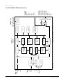
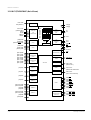
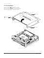
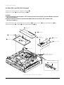
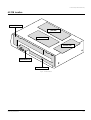
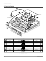
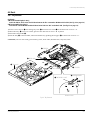
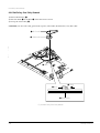
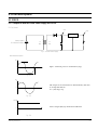
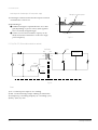
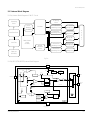
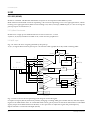
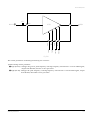
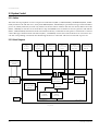
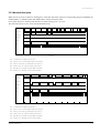
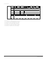
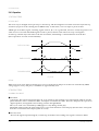
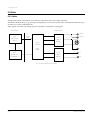
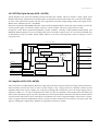
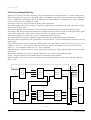
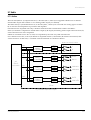
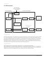
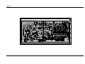
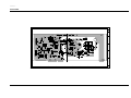
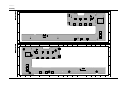
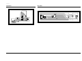
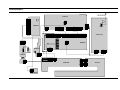
1
DVD PLAYER DVD-C600 SERVICE MANUAL SERVICE Manual DVD-C600 DVD PLAYER CONTENTS 1. Precautions 2. Reference Information ELECTRONICS 3. Product Specification 4. Disassembly and Reassembly 5. Circuit Descriptions 6. Troubleshooting 7. Exploded Views and Parts List DOLBY DIGITAL DECODER BUILT-IN DVD / VIDEO-CD / CD PLAYER DVD-C700 5 DIGITAL VIDEO 8. Electrical Parts List 9. Block Diagrams SPATIALIZER N-2-2 10. PCB Diagrams 11. Wiring Diagram 12. Schematic Diagrams © Samsung Electronics Co., Ltd. FEB. 2000 Printed in Korea AH68-00387A 1. Precautions 1-1 Safety Precautions 1) Before returning an instrument to the customer, always make a safety check of the entire instrument, including, but not limited to, the following items: (1) Be sure that no built-in protective devices are defective or have been defeated during servicing. (1)Protective shields are provided to protect both the technician and the customer. Correctly replace all missing protective shields, including any remove for servicing convenience. (2)When reinstalling the chassis and/or other assembly in the cabinet, be sure to put back in place all protective devices, including, but not limited to, nonmetallic control knobs, insulating fish papers, adjustment and compartment covers/shields, and isolation resistor/capacitor networks. Do not operate this instrument or permit it to be operated without all protective devices correctly installed and functioning. (2) Be sure that there are no cabinet openings through which adults or children might be able to insert their fingers and contact a hazardous voltage. Such openings include, but are not limited to, excessively wide cabinet ventilation slots, and an improperly fitted and/or incorrectly secured cabinet back cover. (3) Leakage Current Hot Check-With the instrument completely reassembled, plug the AC line cord directly into a 120V AC outlet. (Do not use a isolation transformer during this test.) Use a leakage current tester or a metering system that complies with American National Standards institute (ANSI) C101.1 Leakage Current for Appliances and Underwriters Laboratories (UL) 1270 (40.7). With the instrument’s AC switch first in the ON position and then in the OFF position, measure from a known earth ground (metal water pipe, conduit, etc.) to all exposed metal parts of the instrument (antennas, handle brackets, metal cabinets, screwheads, metallic overlays, control shafts, etc.), especially any exposed metal parts that offer an electrical return path to the chassis. Any current measured must not exceed 0.5mA. Reverse the instrument power cord plug in the outlet and repeat the test. See Fig. 1-1. Any measurements not within the limits specified herein indicate a potential shock hazard that must be eliminated before returning the instrument to the customer. (READING SHOULD NOT BE ABOVE 0.5mA) LEAKAGE CURRENT TESTER DEVICE UNDER TEST TEST ALL EXPOSED METER SURFACES 2-WIRE CORD ALSO TEST WITH PLUG REVERSED (USING AC ADAPTER PLUG AS REQUIRED) EARTH GROUND Fig. 1-1 AC Leakage Test (4) Insulation Resistance Test Cold Check-(1) Unplug the power supply cord and connect a jumper wire between the two prongs of the plug. (2) Turn on the power switch of the instrument. (3) Measure the resistance with an ohmmeter between the jumpered AC plug and all exposed metallic cabinet parts on the instrument, such as screwheads, antenna, control shafts, handle brackets, etc. When an exposed metallic part has a return path to the chassis, the reading should be between 1 and 5.2 megohm. When there is no return path to the chassis, the reading must be infinite. If the reading is not within the limits specified, there is the possibility of a shock hazard, and the instrument must be re-pared and rechecked before it is returned to the customer. See Fig. 1-2. Antenna Terminal Exposed Melal Part ohm ohmmeter Fig. 1-2 Insulation Resistance Test Samsung Electronics 1-1 Precautions 2) Read and comply with all caution and safety related notes non or inside the cabinet, or on the chassis. 3) Design Alteration Warning-Do not alter of add to the mechanical or electrical design of this instrument. Design alterations and additions, including but not limited to, circuit modifications and the addition of items such as auxiliary audio output connections, might alter the safety characteristics of this instrument and create a hazard to the user. Any design alterations or additions will make you, the service, responsible for personal injury or property damage resulting therefrom. 4) Observe original lead dress. Take extra care to assure correct lead dress in the following areas: (1) near sharp edges, (2) near thermally hot parts (be sure that leads and components do not touch thermally hot parts), (3) the AC supply, (4) high voltage, and (5) antenna wiring. Always inspect in all areas for pinched, out-of-place, or frayed wiring, Do not change spacing between a component and the printed-circuit board. Check the AC power cord for damage. 1-2 5) Components, parts, and/or wiring that appear to have overheated or that are otherwise damaged should be replaced with components, parts and/ or wiring that meet original specifications. Additionally, determine the cause of overheating and/or damage and, if necessary, take corrective action to remove any potential safety hazard. 6) Product Safety Notice-Some electrical and mechanical parts have special safety-related characteristics which are often not evident from visual inspection, nor can the protection they give necessarily be obtained by replacing them with components rated for higher voltage, wattage, etc. Parts that have special safety characteristics are identified by shading, an ( )or a ( )on schematics and parts lists. Use of a substitute replacement that does not have the same safety characteristics as the recommended replacement part might created shock, fire and/or other hazards. Product safety is under review continuously and new instructions are issued whenever appropriate. Samsung Electronics Precautions 1-2 Servicing Precautions CAUTION : Before servicing Instruments covered by this service manual and its supplements, read and follow the Safety Precautions section of this manual. Note : If unforseen circument create conflict between the following servicing precautions and any of the safety precautions, always follow the safety precautions. Remember: Safety First. 1-2-1 General Servicing Precautions (1) a. Always unplug the instrument’s AC power cord from the AC power source before (1) re-moving or reinstalling any component, circuit board, module or any other instrument assembly, (2) disconnecting any instrument electrical plug or other electrical connection, (3) connecting a test substitute in parallel with an electrolytic capacitor in the instrument. b. Do not defeat any plug/socket B+ voltage interlocks with which instruments covered by this service manual might be equipped. c. Do not apply AC power to this instrument and /or any of its electrical assemblies unless all solid-state device heat sinks are correctly installed. d. Always connect a test instrument’s ground lead to the instrument chassis ground before connecting the test instrument positive lead. Always remove the test instrument ground lead last. (4) An insulation tube or tape is sometimes used and some components are raised above the printed wiring board for safety. The internal wiring is sometimes clamped to prevent contact with heating components. Install such elements as they were. (5) After servicing, always check that the removed screws, components, and wiring have been installed correctly and that the portion around the serviced part has not been damaged and so on. Further, check the insulation between the blades of the attachment plug and accessible conductive parts. 1-2-2 Insulation Checking Procedure Disconnect the attachment plug from the AC outlet and turn the power ON. Connect the insulation resistance meter (500V) to the blades of the attachment plug. The insulation resistance between each blade of the attachment plug and accessible conductive parts(see note) should be more than 1 Megohm. Note : Accessible conductive parts include metal panels, input terminals, earphone jacks, etc. Note : Refer to the Safety Precautions section ground lead last. (2) The service precautions are indicated or printed on the cabinet, chassis or components. When servicing, follow the printed or indicated service precautions and service materials. (3) The components used in the unit have a specified flame resistance and dielectric strength. When replacing components, use components which have the same ratings. Components i-entified by shading, by( ) or by ( ) in the circuit diagram are important for safety or for the characteristics of the unit. Always replace them with the exact replacement components. Samsung Electronics 1-3 Precautions 1-3 ESD Precautions Electrostatically Sensitive Devices (ESD) Some semiconductor (solid state) devices can be damaged easily by static electricity. Such components commonly are called Electrostatically Sensitive Devices(ESD). Examples of typical ESD devices are integrated circuits and some field-effect transistors and semiconductor chip components. The following techniques should be used to help reduce the incidence of component damage caused by static electricity. (1) Immediately before handling any semiconductor component or semiconductor-equipped assembly, drain off any electrostatic charge on your body by touching a known earth ground. Alternatively, obtain and wear a commercially available discharging wrist strap device, which should be removed for potential shock reasons prior to applying power to the unit under test. (7) Immediately before removing the protective materials from the leads of a replacement ESD device, touch the protective material to the chassis or circuit assembly into which the device will be installed. CAUTION : Be sure no power is applied to the chassis or circuit, and observe all other safety precautions. (8) Minimize bodily motions when handling unpackaged replacement ESD devices. (Otherwise harmless motion such as the brushing together of your clothes fabric or the lifting of your foot from a carpeted floor can generate static electricity sufficient to damage an ESD device). (2) After removing an electrical assembly equipped with ESD devices, place the assembly on a conductive surface such as aluminum foil, to prevent electrostatic charge buildup or exposure of the assembly. (3) Use only a grounded-tip soldering iron to solder or unsolder ESD devices. (4) Use only an anti-static solder removal devices. Some solder removal devices not classified as “anti-static” can generate electrical charges sufficient to damage ESD devices. (5) Do not use freon-propelled chemicals. These can generate electrical charges sufficient to damage ESD devices. (6) Do not remove a replacement ESD device from its protective package until immediately before your are ready to install it.(Most replacement ESD devices are packaged with leads electrically shorted together by conductive foam, aluminum foil or comparable conductive materials). 1-4 Samsung Electronics Precautions 1-4 Handling the optical pick-up The laser diode in the optical pick up may suffer electrostatic breakdown because of potential static electricity from clothing and your body. WRIST-STRAP FOR GROUNDING 1M The following method is recommended. (1) Place a conductive sheet on the work bench (The black sheet used for wrapping repair parts.) (2) Place the set on the conductive sheet so that the chassis is grounded to the sheet. (3) Place your hands on the conductive sheet(This gives them the same ground as the sheet.) (4) Remove the optical pick up block (5) Perform work on top of the conductive sheet. Be careful not to let your clothes or any other static sources to touch the unit. THE UNIT 1M CONDUCTIVE SHEET Fig.1-3 (6) Short the short terminal on the PCB, which is inside the Pick-Up ASS’Y, before replacing the PickUp. (The short terminal is shorted when the PickUp Ass’y is being lifted or moved.) (7) After replacing the Pick-up, open the short terminal on the PCB. Be sure to put on a wrist strap grounded to the sheet. Be sure to lay a conductive sheet made of copper etc. Which is grounded to the table. Samsung Electronics 1-5 Precautions 1-5 Pick-up disassembly and reassembly 1-5-1 Disassembly 1-5-2 Assembly 1) Remove the power cable. 2) Switch SW1 on Deck PCB to “OFF” before removing the FPC. ( Inserted into Main PCB MCN06. See Fig. 1-4) 3) Disassemble the Deck. 4) Disassemble the Deck PCB. 1) Replace the Pick-up. 2) Assemble the Deck PCB. 3) Reassemble the Deck. 4) Insert FPC into Main PCB MCN06 and switch SW1 on Deck PCB to “ON”. (See Fig 1-4) Note : If the assembly and disassembly are not done in correct sequence, the Pick-up may be damaged. FPC TO MAIN PCB (MCN06) SW1 OFF ON Fig. 1-4 1-6 Samsung Electronics 2. Reference Information 2-1 IC Dsecriptions 2-1-1 AIC1 (AK4324 ; Digital-to-Analog Converter) DIF0 LRCK BICK SDATA DIF1 DIF2 DEM0 AVDD AVSS De-emphasis Control Serial Input Interface PD DEM1 DZFL AOUTL+ 8X Interpolator ∆∑ Modulator SCF 8X Interpolator ∆∑ Modulator SCF AOUTL- SMUTE DFS AOUTR+ AOUTR- Clock Divider DZFR MCLK PIN I / O NAME CKS DVDD FUNCTION DVSS VREF PIN I / O NAME FUNCTION 13 I DIF0 Digital input format pin 1 - DVSS Digital ground pin 2 I DVDD Digital power supply 14 I DIF1 Digital input format pin 3 I CKS Master clock select pin (Internal pull-down pin) Nomal speed "L":MCLK = 256fs, "H":MCLK = 384fs Double speed "L":MCLK = 128fs, "H":MCLK = 192fs 15 I DIF2 Digital input format pin 4 I MCLK Master clock input pin 16 0 AOUTR- Rch negative analog output pin 5 I PD Power-Down mode pin. When at "L", the AK4324 is in power-down and is held in rest. The AK4324 should always be reset upon power-pin 17 O AOUTR+ Rch positive analog output pin 6 I BICK Audio serial data input pin 64fs clock is recommended to be input on this pin 18 O AOUTL- Lch negative analog output pin 7 I SDATA Audio serial data input pin 2's complement MSB-first data is input on this pin. 19 O AOUTL+ Lch positive analog output pin 8 I LRCK L/R clock pin. 20 - AVSS Analog ground pin 9 I SMUTE Soft mute pin When this pin goes "H", soft mute cycle is initiated When returning "L", the output mute releases. 21 O VREF Voltage reference input pin 10 I DFS Double speed sampling mode pin (Internal pull-down pin) "L":normal speed, "H":double speed 22 O AVDD Analog power supply pin. 11 I DEM0 De-emphasis frequency select pin 23 O DZFR Rch zero input detect pin 12 I DEM1 De-emphasis frequency select pin 24 O DZFL Lch zero input detect pin Note : Allinput pins except internal pull-down pins should not be left floating. Samsung Electronics 2-1 Reference Information 2-1-2 RIC1 (KS1461 ; RF) 83 82 81 80 79 78 77 76 AGC-HOLD(OOH) ADVD 5 AGC_DET RF MUX BCA BLOCK 74 BCAI RF Equalizer RF SLM & AGC C D BCA RFRP GAIN_EQ(02H) CDRSEL(00H) TE1RES DELAY_SEL(OOH) PLLCTL TBAL(O1H) RREFEQ 10 VREF GENERATOR DELAY D GCA RREF 11 CD1 S12 DVD1 DVD2 LDONB FLT_CTL CDRSEL TESEL AGC-HOLD TBAL GAIN_TE3 ENV_SEL DVCTL_SEL DPD_MUTE GAIN_EQ GAIN_FE GAIN_ABCD TE_OFST FE_OFST ABCD_OFST DELAY_CD DELAY_AB PDLIMIT ga_RFSUM HOLD_CTL ga_PLLDP ga_PLLDN HOLD_CTL(O8H) DPDMUTE DPD_MUTE(O2H) SEOFHOLD FLT_CTL(OOH) CAL_ENDB(O2H) DPDEQ1 9 PD,LPF COM EQ D TEOPST(04H) MUX3 PDLIMITRES TE1_LIMIT D GCA COM EQ D DPDEQ2 FAULTOUT VREFEQ 12 EQ VC AMP GAIN_TE3(02H) E 13 DELAY_SEL(00H) PLLCTL TE38 F 14 AUTO OFSTCTL RFCT & MIRR CD1 S12 DVD1.2 RREFBF CB 2 84 RFCT 85 CP 2 86 RFRP 87 RFRPN 88 CB 1 B 8 89 MROFST A 4 DDVD CP 1 3 DCD 7 MIRRI 2 6 90 75 BCAO BCD BDVD 91 MUX CCD CDVD EQVCC 1 RFEQO ACD BCATH EQGND to RF EQ TUNING BLOCK EQIN AGCLEVEL 92 RFAGCO AGCB 93 AGCI AGCP 94 AGCC RDPF 95 EQF PLLGF 99 98 97 96 EQG VZOCTL 100 72 OSC 71 STB S/IF BLOCK 70 CLOCK 69 DATA 68 RREFDLY DPD BLOCK 67 VREFDPD 66 DPDGND 65 TE1RES GCA 64 PLLCTL OFSTHOLD TBAL(01H) TEOFST(04H) 63 DPDMUTE to DPD BLOCK 62 FAUL TOUT CDRSEL(OOH) GAIN_ABCD(OOH) ADVD1 15 61 DPDEQ2 60 DPDEQ1 BDVD1 16 CDVD1 17 DDVD1 18 SUB RF MUX ACD1 19 BCD1 20 D1 B1 C1 A1 ABCD SUM EQIN 59 TE30FST ENV_SEL(02H) GAIN_FE(03H) 58 BCA 57 MIRR OFSTHOLD MUX CCD1 21 ABCD_OFST(O6H) FE 56 DPDVCC FE_0FST(05H) DCD1 22 OFSTHOLD AVCC 23 VREFA 24 73 RESET CDRSEL(00H) LDONB(00H) ANALOG VC AMP 55 DFCT2 MUX 54 DFCT1 TESEL(OOH) ENVELOPE FOK 53 DFCTTH1 DEFECT 52 DFCTTH2 ALPC FOFST 25 FOFST 35 36 37 38 39 40 41 42 43 44 45 46 47 48 49 50 VREFLP_BGI LDODVD AGND FE FEN TEN TE PDLIMITRES ABCD ABCDI ENVP DGND FOKTH FOKB DFCT_CP1 DFCT_CP2 CC1 CC2 ENV 34 ENVB 33 ABCDN 32 PDCD 28 29 30 31 LDOCD 27 PDVD 26 OFSTHOLD 2-2 51 DVCC Samsung Electronics Samsung Electronics CD optical laser monitor diode voltage input port Power GND port for analog part FE AMP output port I O I P O PDDVD LDOCD PDCD AGND FE 30 31 32 33 FEN FE Input port for AMP GAIN setting - DPD EQ (A+C) output port DPD EQ (B+D) output port O O TE3OFST DPDEQ1 DPDEQ2 59 60 61 CD optical laser diode driving voltage output port DVD optical laser monitor diode voltage input port DVD optical laser diode driving voltage output port 64 63 PLLCTL DPDMUTE I I DPD TE PLL variable input port DPD TE MUTE control port (H : MUTE) DPD defect waveform output port (MONITOR) Resistance connection port for 3BTE offset - BANDGAP voltage input port for ALPC O BCA output port O BCA 58 FAULTOUT Mirror output port O MIRR 57 ON/OFF connection port for auto offset block (L : auto offset adjustment H : serial offset adjustment) 62 Power voltage input port for DPD TE P DPDVCC 56 center voltage, Use at other block CAP connection port for focus auto offset (OPEN) Defect output port for SERVO parating level setting Defect output port for PLL O O DFCT1 DFCT2 54 DFCTTH1 - DVCTTH2 52 53 Power voltage input port for digital circuit P DVCC 51 Resistance connection port for PLL defect comparating level setting Resistance connection port for SERVO defect com- AC coupling input port for defect I CC2 50 Output port of peak detector for defect O - CC1 DFCT_CP2 Focus OK comparator output port (L: FOCUS OK) Peak hold time constant connection port SERVO defect max. time setting Peak hold time constant connection port PLL defect min. time setting 49 48 - O FOKB 46 DFCT_CP1 I FOKTH 45 47 Power GND input port for digital circuit P DGND 44 Focus OK comparing level input port RF envelope detect output port 95 94 93 92 91 90 AGCP AGCB AGCLEVEL EQGND AGCI AGCC RFAGCO EQIN 88 89 BCATH RFEQO EQVCC MIRRI CP1 CB1 MROFST RFRPN RFRP CP2 CB2 RFCT BCAO BCAI RESET OSC STB CLOCK DATA RREFDLY VREFDPD DPDGND TE1RES PIN NAME 87 86 85 84 83 82 81 80 79 78 77 76 75 74 73 72 connection port for RF envelope detect Bottom hold time constant setting RC connection port for RF envelope detect 71 ABCD AC coupling input port for SERVO monitor 70 69 68 67 66 65 Peak hold time constant setting RC ABCD AMP output port Input port for ABCD AMP GAIN setting Bias resistance port for PDLIMIT TE AMP output port Input port for TE AMP GAIN setting O - - I O I - O I I FUNCTION ENV ENVB ENVP ABCDI ABCD ABCDN PDLIMTRES TE TEN I/O 43 42 41 40 39 38 37 36 35 34 PIN NAME 55 CAP connection port for analog part 29 I I O -/O O Power voltage input port for analog part P LDODVD CD optical main beam F input port for SERVO I 28 CD optical main beam F input port for SERVO I BCD1 20 VREFLP_BGI CD optical main beam F input port for SERVO I ACD1 19 27 CD optical main beam F input port for SERVO I DDVD1 18 OFSTHOLD DVD optical main beam D input port for SERVO I CDVD1 17 26 DVD optical main beam C input port for SERVO I BDVD1 16 FOFST DVD optical main beam B input port for SERVO I ADVD1 15 25 DVD optical main beam A input port for SERVO I F 14 VREFA CD optical sub beam F input port for SERVO I E 13 24 CD optical sub beam E input port for SERVO I VREFEQ 12 AVCC CAP connection port for RF EQ center voltage O RREF 11 23 Analog block bias resistance connection port - CCD1 RF EQ bias resistance connection port - RREFEQ 10 DCD1 RF AMP I/O buffer bias resistance connection port - RREFBF 9 22 DVD optical main beam D AC coupling input port for RF 21 DVD optical main beam C AC coupling input port for RF I DVD optical main beam B AC coupling input port for RF I BDVD 6 I DVD optical main beam A AC coupling input port for RF I ADVD 5 CDVD CD optical main beam D AC coupling input port for RF I DCD 4 DDVD CD optical main beam C AC coupling input port for RF I CCD 3 8 CD optical main beam B AC coupling input port for RF I BCD 7 CD optical main beam A AC coupling input port for RF I ACD 1 FUNCTION I/O 2 PIN NAME - - I P I - RF peak hold time constant RC connection port for RF AGC RF bottom hold time constant RC connection port for RF AGC AGC level control voltage input port Power GND input port for RF EQ When AGC is “HOLD”, AGC voltage input port AGC time constant CAP connection port RF AGC AMP output port RFAGCO input port for RF EQ O BCA comparating level control port I RF EQ output port Power voltage input port for RF EQ Input port for MIRR signal generation Peak hold time constant RC connection port for RFCT generation RFCT generation Bottom hold time constant RC connection port for RF ripple offset control port for mirror RF ripple AMP GAIN input port for mirror RF ripple AMP output port for mirror RFCT generation Peak hold time constant RC connection port for RFCT generation Bottom hold time constant RC connection port for RF ripple center voltage output port for mirror BCA FILTER2 BCA FILTER1 Reset input port for auto offset block (L : RESET) OSC time constant input port for auto offset block Data enable input port Clock input port Data input port Bias resistance connection port for delta block CAP connection port for DPD TE center Power GND input port for DPD TE DPD TE PLL variable bias resistance FUNCTION I O P I - - I I O - - O O I I I I I - O P I I/O 100 VZOCTL PLLGF EQF 98 99 EQG RDPF 97 96 PIN NAME RF EQ control port (When No. PLLG isn’t adjusted, apply DC CTL voltage.) RF EQ peak frequency control voltage input port I I RF EQ boost gain control voltage input port I RF EQ boost, peak frequency gain control port corresponding to wideband PLL (PLLG. PLLF resistance internal design) Bias resistance connection port for RF EQ frequency setting - I FUNCTION I/O Reference Information 2-3 2-4 EFMOA EFM ASYCD ASYDVD RFI EFMI DVCTL TBAL FBAL SPD SLD TRD FOD RSTB COUT TILTO FE EFM ASYMETRY D/A CONVERTER BLOCK TRACK COUNTER ROM DSP CORE FOR DIGITAL SERVO PS1 WIDE CAPTURE RANGE PLL SYSCON INTERFACE BLOCK SUB CODE READ BLOCK SSTOP /PSO TE TEST SME XI A/D CONVERTER BLOCK XO TZCO XOUT I/O INTERFACE BLOCK LOCK TIMING GENERATOR SMON ENV VREF PLLHD INTO_224 FDCTL MAGICO EQCTL VCTRL RVCO PLCK EFMRTD RPD PLLLOCK RFD MDOUT[3:0] PSB SENSE MDATA[7:0] MRDB MWRB CSB DAB SCOR SQSI SQCK LDONB TLKB FLKB Reference Information 2-1-3 SIC1 (KS1452 ; Digital Servo) DIRC DFCT FOKB MIRR TZCA PHI1 TILTI Samsung Electronics Samsung Electronics Counter clock Focus servo lock signal output pin Tracking servo lock signal output pin 0 : 1BIT System reset signal input pin Micom chip select pin Micom data/address select pin Micom write clock signal input pin O O I I I I I FLKB TLKB PSB RSTB CSB DAB MWRB 6 7 8 9 10 11 12 Micom read clock signal input pin Micom data pin 0 Micom data pin 1 Micom data pin 2 Micom data pin 3 Micom data pin 4 Micom data pin 5 Micom data pin 6 Micom data pin 7 Internal status monitor pin Servo logic & ROM VDD power supply pin System clock signal input pin System clock signal output pin Clock out (33.9688MHz) to DSP Servo logic & ROM VSS power supply pin Clock output pin for subcode data read Subcode data input pin Timing detection input pin for subcode data read Motor ON signal input pin Lock signal input pin Direct jump control (for 1 track jump) I I/O I/O I/O I/O I/O I/O I/O I/O O P I O O P O I I I I I MRDB MDATA0 MDATA1 MDATA2 MDATA3 MDATA4 MDATA5 MDATA6 MDATA7 SENSE DVDD XI XO XOUT DVSS SQCK SQSI SCOR SMON LOCK DIRC 13 14 15 16 17 18 19 20 21 22 23 24 25 26 27 28 29 30 31 32 33 1 : 8BIT Test pin (L : normal H : test) I O TEST COUT Sled motor position sensor input pin 1 I PS1 3 5 Limit switch/sled position sensor input pin0 I 4 Mode data3 out controlled by micom O MDOUT3 SSTOP/PSO FUNCTION 1 I/O 2 PIN NAME 64 63 62 61 60 59 58 57 56 55 54 53 52 51 50 49 48 47 46 45 44 43 42 41 40 39 38 37 36 35 34 TE VREF SME AVSS SVSS RFI LPFCD LPFDVD EFMO EFMI EQCTL SVDD TZCO EFMOA MAGICO VCTL RPD RFD RVCO PVSS EFMRTD PLLLOCK PLCK PVDD INTO_224 PLLHD MIRR DFCT LDONB FDCTL FOKB PIN NAME PLL logic block VSS power supply pin Resistor pin for VCO GAIN Gain adjust resister for frequence detector Gain adjust resister for phase detector Control voltage for VCO P I I I I EFM offset adjustment pin Tracking zero cross output pin Servo CPU VDD power supply pin EQ control signal EFM signal for test EFM signal Asymmetric input signal for DVD Asymmetric input signal for CD RF input signal Servo CPU VSS power supply pin Analog block VSS power supply pin Spindle error input pin Reference voltage input pin Tracking error signal input pin I O P O I O I I I P P I I I Input for hysteresis control of FD output (for test) Latched EFM output signal O I Frequency lock detect output (H : Lock L : Unlock) PLCK PLL logic block VDD power supply pin Servo interrupt monitor pin PLL hold signal from micom Mirror signal input pin Defect Detection signal input pin Laser diode ON signal output pin PLL frequency detect control input pin Focus OK signal input pin FUNCTION O O P O I I I O I I I/O 72 71 70 69 68 67 66 65 FBAL TBAL DVCTL TILTO AVDD TILTI ENV FE PIN NAME O O O O P I I I I/O Focus balance signal output pin Tracking balance signal output pin Depth variation control signal output pin Tilt out (reserved) Analog block VDD power supply pin Tilt in (reserved) RF envelope input pin Focus error signal input pin FUNCTION Tracking actuator drive signal output pin TE signal for tracking zero cross input pin Mode data 0 out controlled by micom Mode data 1 out controlled by micom Mode data 2 out controlled by micom O I O O O TRD TZCA MDOUT0 MDOUT1 MDOUT2 78 79 80 O FOD 75 77 Focus actuator drive signal output pin O 76 Sled motor drive signal output pin Spindle motor drive signal output pin O SLD SPD 74 FUNCTION I/O 73 PIN NAME Reference Information 2-5 2-6 FG MON MDP MDS FSW PLL_LOCK CLV_LOCK SERVO_LOCK XTI1 XTO1 CK33MI CK33MO TO (12) EFMI PLCK BCARZ FROM R/F, PLL(3) CD CLV/CAV WFCK 17.58/7.35KHz M SUBCODE I/F 23BIT SR CD-G M SQ-VCD DVDP, MICOM I/F M TEST0, TEST1, TEST2 V-CD, CD-DA DEINTERLEAVE & RAM CONTROL (6, 4, 3) trans ID ECC EDC DESCRAMBLER TO MICOM (15) MDAT(7:0), MRZA, ZCS, MWR, MRD, ZIRQZD, ZWAIT, ZRST Power(34)=VDD(11)+GND(23) Test Pin(3) EFM DEMOD (32, 28, 5) (28, 24, 5) CIRC 75Hz 676.08Hz (208, 192, 17) (182, 172, 11) ECC (6, 4, 3) efmwr ID ECC 16-8 DEMOD FRAME SYNC DET/PROT/INS (7.35KHz) VCO TIMING GENERATOR 7.35KHz = 4.3218M/588 17.58KHz = 26.16M/1488 ECSY Monitor(8) GFS, FRSYZ, TX, EFMO, WFCK, RFCK, CK 16M, DEMPHA M DVD CLV/CAV RFCK 17.58/7.35KHz X'TAL & TIMING GEN VCO TIMING GENERATOR 26.16MHz FRAME SYNC DET/PROT/INS (17.57KHz) 32BIT SR PWMO(7:0) TO D-EQ (8) SDATA[0] / CDATA SDATA[1] / LRCK SDATA[2] / BCLK SDATA[3] / C2PO SDATA[4] / SQDT SDATA[5] / WFSY SDATA[6] / SOS1 SDATA[7] / SQCK DATREQ CSTROBE DTER DATACK TOS TO AV (13) DD(15:0) DADR(8:0) ZRAS ZUCAS ZLCAS ZOE(1:0) ZWE(1:0) TO DRAM 256K*16 (32) Reference Information 2-1-4 DIC1 (KS1453 ; DVD Data Processor) Samsung Electronics Samsung Electronics DD5_BI DVSS DD9_BI 31 32 20 DD10_BI DD1_BI 19 30 DD14_BI 18 29 DD0_BI 17 DD4_BI DD15_BI 16 28 DVSS 15 DD11_BI XTO_OUT 14 27 XTI_IN 13 DVDD DVDD 12 26 MDAT0_BI 11 DD3_BI MDAT1_BI 10 25 MDAT2_BI 9 DD12_BI MDAT3_BI 8 24 MDAT4_BI 7 DD2_BI MDAT5_BI 6 23 MDAT6_BI 5 DVSS MDAT7_BI 4 DD13_BI DVSS 3 22 MRZA_IN 2 21 DVSS ZCS_IN 1 NAME PIN DRAM data bus Digital GND (0V) DRAM data bus DRAM data bus DRAM data bus DRAM data bus Digital power (+5V) DRAM data bus DRAM data bus DRAM data bus DRAM data bus Digital GND (0V) DRAM data bus DRAM data bus DRAM data bus DRAM data bus Digital GND (0V) System clock output for 26.16 MHz System clock input for 26.16 MHz Digital power (+5V) Micom data bus Micom data bus Micom data bus Micom data bus Micom data bus Micom data bus Micom data bus Micom data bus Digital GND (0V) (L -> Register H -> Data) Micom register select Chip select (Active Low) Digital GND (0V) FUNCTION 65 64 63 62 61 60 59 58 57 56 55 54 53 52 51 50 49 48 47 46 45 44 43 42 41 40 39 38 37 SDATA5_OUT SDATA4_OUT SDATA3_OUT SDATA2_OUT SDATA1_OUT SDATA0_OUT DVDD DATACK_OUT TOS_OUT DVSS DVSS DADR3_OUT DADR4_OUT DADR2_OUT DADR5_OUT DADR1_OUT DADR6_OUT DADR0_OUT DVSS DADR7_OUT DADR8_OUT ZRAS_OUT ZOEO_OUT DVDD ZOE1_OUT ZWE0_OUT ZWE1_OUT ZUCAS_OUT ZLCAS_OUT DVSS DD7_BI 35 36 DD8_BI DD6_BI NAME 34 33 PIN DVD data/Sub code frame sink (WFSY) DVD data/Sub code serial data (SQDT) DVD data/CD data error flag (C2P0) DVD data/CD data bit clock (BLCK) DVD data/CD data L/R clock (LRCK) DVD data/CD data bitstream output Digital power (+5V) Data acknowledge signal output Top of sector Digital GND (0V) Digital GND (0V) DRAM address bus DRAM address bus DRAM address bus DRAM address bus DRAM address bus DRAM address bus DRAM address bus Digital GND (0V) DRAM address bus DRAM address bus DRAM row address strobe DRAM output enable 0 Digital power (+5V) DRAM output enable 1 (16M, --------, 16M) DRAM write enable 0 (4M, 8M, 16M) DRAM write enable 1 (8M ONLY) DRAM upper column address strobe DRAM row column address strobe Digital GND (0V) DRAM data bus DRAM data bus DRAM data bus FUNCTION SDATA7_BI DVSS 67 68 97 96 95 94 93 92 91 90 89 88 87 86 85 84 83 82 81 80 79 78 77 76 75 74 73 72 71 70 DVSS CK33MO_OUT CK33MI_IN DVSS GFS_OUT TX_OUT FRSYZ_OUT DVSS DVSS DVSS DVSS DVDD DVDD DVSS DVSS DVSS PWM00_OUT PWM01_OUT PWM02_OUT PWM03_OUT DVDD PWM04_OUT PWM05_OUT PWM06_OUT PWM07_OUT DVSS DTER_OUT DATREQ_IN CSTROBE_OUT SDATA6_OUT 66 69 NAME PIN Digital GND (+5V) System clock output for 33.8688MHz System clock input for 33.8688MHz Digital GND (0V) Good frame sync detection result output (“H” active) Digital out Frame sync out Digital GND (0V) Digital GND (0V) Digital GND (0V) Digital GND (0V) Digital power (+5V) Digital power (+5V) Digital GND (0V) Digital GND (0V) Digital GND (0V) PWM output signal PWM output signal PWM output signal PWM output signal Digital power (+5V) PWM output signal PWM output signal PWM output signal PWM output signal Digital GND (0V) DVD data error output Data request from A/V decoder or ROM decoder Data strobe (clock) output Digital GND (0V) DVD data/Sub code serial clock (SQCK) DVD data/Sub code block sink (S0S1) FUNCTION 128 127 126 125 124 123 122 121 120 119 118 117 116 115 114 113 112 111 110 109 108 107 106 105 104 103 102 101 100 99 98 PIN MWR_IN MRD_IN ZIRQZD_OUT ZWAIT_OUT ZRST_IN DVSS BCARZ_IN DEMPHA_OUT CK16M_OUT DVDD DVDD DVDD EFMI_IN FSW_OUT FG_IN MON_OUT DVSS DVSS MDS_OUT MDP_OUT SERLOCK_OUT CLVLOCK_OUT PLLLOCK_OUT DVSS PLCK_IN RFCK_OUT WFCK_OUT EFMO_OUT TEST2_IN TEST1_IN TEST0_IN NAME Micom write strobe (schmidt trigger) Micom read strobe (schmidt trigger) Interrupt request from micom Micom read/write access wait (“L” wait) Hardware reset active low Digital GND (0V) BCA input signal When DEEMPHASIS is ON, “HIGH”. 2∫–¡÷ clock of CK33M/16.934MHz Digital power (+5V) Digital power (+5V) Digital power (+5V) EFM/EFM+ signal input state) Spindle motor output filter conversion output (3- Reference signal for CAV Spindle motor ON/OFF control output Digital GND (0V) Digital GND (0V) Spindle motor speed control signal (3-state) Spindle motor phase control signal (3-state) Lock signal for SERVO Lock signal for CLV Lock signal for PLL Digital GND (0V) Phase locked clock Reference frame pulse Write frame pulse EFM out Test mode setting port Test mode setting port Test mode setting port FUNCTION Reference Information 2-7 Reference Information 2-1-5 DIC2 (KM416C254BJ-6 ; CMOS DRAM) BLOCK DIAGRAM RAS UCAS Control LCAS Clocks Vcc VBB Generator Vss W Refresh Timer Row Decoder Lower Data in Buffer Refresh Control Lower DQ0 to DQ7 Data out Memory Array Refresh Counter Buffer 262,144 x 16 Upper Cells Data in Buffer Row Address Buffer AO . . Upper OE DQ8 to DQ15 Data out Col. Address Buffer A8 Column Decoder FUNCTION NAME A0-A8 DQ0-15 Address Inputs Data in/Out VSS Ground RAS Row Address Strobe UCAS Upper Column Address Strobe LCAS Lower Column Address Strobe W Read/Write Input OE Data Output Enable V CC Buffer Power (+5V) Power (+3.3V) N.C 2-8 No Connection Samsung Electronics Reference Information 2-1-6 VIC1 (ZiVA-3 ; Audio/Video Decoder) BLOCK DIAGRAM ZiVA-3 Decoder OSD Decoder SDRAM/ EDO/ROM Interface Memory Controller Subpicture Decoder Host Interface Host Interface Control Logic MPEG Video Decoder Secure View CD-DA and LPCM Decoder CSS Descrambling Program DVD/CD Interface Stream Decoder Bus Key Dolby Digital Audio Decoder Authentication (Optional) Audio DSP Video Mixer Video Interface Digital Audio Interface Audio Interface Scrambled, Compressed Content Descrambled, Compressed Content MPEG Audio Decoder Decompressed Content Display Content LOGIC DIAGRAM DA-DATA[0:3] CS Host Interface Signals DTACKSEL DA-LRCK HADDR[2:0] DA-BCK Interface RD DA-XCK Signals DA-IEC HDATA[7:0] WAIT/DTACK INT EDO-CAS HOST8SEL EDO-RAS R/W Video Audio LDQM VDATA[7:0] MDATA[15:0] Interface HSYNC MADDR[20:0] Signals VSYNC MWE VCLK ROM-CS SDRAM/EDO Interface Signals SD-CAS DVD-DATA0/CD-DATA SD-RAS DVD-DATA1/CD-LRCK SD-CLK DVD-DATA2/CD-BCK SD-CAS[1:0] DVD-DATA3/CD-C2PO UDQM DVD-DATA4/CDG-SDATA DVD/CD Interface Signals DVD-DATA5/CDG-VFSY DVD-DATA6/CDG-SOS1 SYSCLK DVD-DATA7/CDG-SCLK VDD VSS VREQUEST A_VSS VSTROBE A_VDD ERROR AREQUEST Samsung Electronics Interface Signals P10[10:0] V-DACK/ASTROBE A-DACK Global RESET ZiVA Decoder 2-9 Reference Information 2-1-7 VIC50 (SAA7128 ; Digital Video Encoder) BLOCK DIAGRAM LLC1 VDDA XCLK TTXRQ RCV2 RCV1 XTAL XTALI SCL SDA RESN 25,28,31,36 4 37 8 43 7 34 35 41 42 40 20 VDD I2C 21 I2 C- SYNC/ INTERFACE CLOCK SA Clock&Timing I2 C-Control I2 C-Control 9..16 I2 C-Control Y Y MP MP(7:0) FADER CbCr D 30 CVBS (CSYNC) 27 VBS (CVBS) 24 C (CVBS) OUTPUT- ENCODER C MP INTERFACE A 44 I2 C-Control TTX 22,32,33 I2 C-Control VSSA 23 Y D R(Cr) RGBCbCr G(Y) 29 B(Cb) 19 RTC1 AP SP FUNCTION NAME res. 1 3 2 VDD VSS I/O 26 A 6,17,39 5,18,38 PIN PROCESSOR Reserved pin, do not connect 2 I SP Test Pin;connected to digital ground for normal operation 3 I AP Test Pin;connected to digital ground for normal operation 4 I LLC1 Line-Locked Clock input;this is the 27 MHz master clock 5 I V SS1 Digital supply ground 1 6 I V DD1 Digital supply 1 7 I/O RCV1 Raster Contral 1 for video port. This pin receives/provides a VS/FS/FSEQ signal. 8 I/O RCV2 Raster Contral 2 for video port. This pin provides an HS pulse of programmable length or receives an HS pulse. 2-10 Samsung Electronics Reference Information PIN I/O 9 I MP7 10 I MP6 11 I MP5 12 I MP4 13 I MP3 14 I MP2 15 I MP1 16 I MP0 17 I V DD2 Digital supply voltage 2 18 I V SS2 Digital ground 2 19 I RTCI 20 I 21 I SA 22 I V SSA1 Analog ground 1 for Red (Cr), C(CVBS), Green(Y) outputs 23 O R(Cr) Analog output of Red (Cr)signal 24 O C 25 I V DDA1 Analog supply voltage 1 for R(Cr), C(CVBS) outputs 26 O G(Y) Analog output of Green(Y) signal 27 O VBS Analog output of VBS (CVBS) signal 28 I V DDA2 Analog supply voltage 2 for VBS(CVBS), Green(Y) outputs 29 O B(Cb) Analog output of Blue(Cb) signal 30 O CVBS Analog output of CVBS(CSYNC) signal 31 I V DDA3 Analog supply voltage 3 for Blue(Cb)and CVBS(CSYNC), outputs 32 I V SSA2 Analog ground 2 for VBS (CVBS), Blue(Cb), CVBS(CSYNC)outputs 33 I V SSA3 Analog ground 3 for the DAC reference ladder and the oscillator 34 O XTAL Crystal oscillator output 35 I XTAL1 36 I V DDA4 Analog supply voltage 4 for the DAC reference ladder and the oscillator 37 O XCLK Clock output of the crystal oscillator 38 I V SS3 Digital supply ground 3 39 I V DD3 Digital supply 3 40 I RESN 41 I SCL 12C serial clock input 42 I/O SDA 12C serial data input/output 43 O TTXRQ 44 I TTX Samsung Electronics FUNCTION NAME VDD 12C Double speed 54 MHzMPEG port. It is an input for "CCIR 656" style multiplexed Cb, Y, Cr data. Data are sampled on the rising and falling clock edge;data sampled on the risting edge then are sent to the encoding part of the device, data sampled on the falling edge are sent to the RGB part of the device. (or vice verse, depending on programming) Real Time Control input. If the LLC1 clock is provided by an SAA7111 or SAA7151B, RTCI should be connected to the RTCO pin of the respective decoder to improve the signal quality. Sense input for 12C bus voltage;connect to 12C bus supply Select 12C address; low selects slave address 88h, high selects slave address 8Ch. Analog output of Chrominance (CVBS) signal Crystal oscillator input; if the oscillator is not used, this pin should be connected to ground. Reset input, active LOW. After reset is applied, all digital I/Os are in input mode; PALBlackburst on CVBS, VBS and C;RGB outputs set to lowest voltage. The 12C-bus receiver waits for the START condition. Teletext Request output, indicating when text bits are requested Teletext bit stream input 2-11 Reference Information 2-1-8 MIC1 (TMP93CM41F ; Main Micom) PAO~PA6 PA7(SCOUT) PORT A VCC[3] VSS[3] 900L-CPU P50 to P57 (ANO to AN7) AVCC AVSS VREFH VREFL 10-BIT 8CH A/D CONVERTER XWA XBC ADE XHL XIX XIY XIZ XSP W B D H A C E L (TXD1)P93 (RXD1)P94 (SCLK1)P95 SERIAL I/O OSC IX IY IZ SP 32bit (TXD0)P90 (RXD0)P91 (SCLK0/CTS0)P92 High Frequency SR (CH,0) P C CLK Low F Frequency OSC SERIAL I/O (CH,1) INTERRUPT (PG 00)P60 (PG 01)P61 (PG 02)P62 (PG 03)P63 (PG 10)P64 (PG 11)P65 (PG 12)P66 (PG 13)P67 (T10)P70 X1 X2 XT1 XT2 AM8/16 EA RESET ALE TEST2,1 CONTROLLER NMI WATCH-DOG WDTOUT PATTERN GENERATOR (CH,0) PATTERN TIMER GENERATOR (CH,1) 2KB RAM PORT 0 P00 to P07 (AD0 to AC7) PORT 1 P10 to P17 (AD8 to AD15/A8 toA15 PORT 2 P20 to P27 (A0 to A7/A16 to A23) 8BIT TIMER (TIMER 0) 8BIT TIMER (T01)P71 (T02)P72 (TIMER 1) 8BIT PWM (TIMER 2) (T03)P73 8BIT PWM (TIMER 3) PORT 3 (INT4/T14)P80 (INT5/T15)P81 (T04)P82 (T05)P83 (INT6/T16)P84 (INT7/T17)P85 (T06)P86 16BIT TIMER (TIMER 4) P30(RD) P31(WR) P32(HWR) P33(WAIT) P34(BUSRQ) P35(BUSAK) P36(R/W) P37(RAS) 16BIT TIMER (TIMER 5) CS/WAIT CONTROLLER (3-BLOCK) P40(CS0/CAS0) P41(CS1/CAS1) P42(CX2/CAS2) (INTO)P87 2-12 Samsung Electronics Samsung Electronics TXD1 094 SCLK1 AM8/16 CLK Vcc Vss X1 X2 /EA /RESET 20 21 22 23 24 25 26 27 28 29 30 TXDO 17 RXDO INTO 16 SCLKO P86 15 19 INT7 14 18 P83 11 /INT6 P82 10 13 INT5 9 12 P73 /INT4 8 P71 P72 7 P70 5 6 AVcc /NMI AVss 2 4 VREFL 1 3 PORT NAME No DSP H/W reset O /MRST /EA X2 X1 GND VCC CLK AM8 MC STB High frequency OSC out External access CS41/CS40 O I Master reset from FRONT High frequency OSC in I I 56 GND - 60 59 58 57 55 - 54 53 Address mode (H: 8 bit mode) Clock output (System clock÷2) 50 I RF control data O MD 49 48 O Serial data clock I 52 Serial data input I TXD SCLK 47 RF control clock Serial data output O RXD 46 O Interrupt from DSP I ZINT 45 51 Request to front micom O RRQ 44 43 42 41 40 39 38 37 36 35 34 33 32 31 No I/O RF data latch - I - PLL CTL Interrupt from spindle motor FG I PLL control DAC rest1 I I Interrupt from front micom I FGINT - Interrupt from AV-DEC O - Non-maskable interrupt I AV-DEC H/W reset A/D VCC input - O A/D GND input O A/D Ref input (L) I - FUNCTION I DRST1 SRQ DVDINT - ZIVA_RST - ZRST - AVCC AGND GND ASSIGNED I/O NAME A15 A14 A13 A12 A11 A10 A9 A8 AD7 AD6 AD5 AD4 AD3 AD2 AD1 AD0 Vcc ALE PA7 PA6 PA5 PA4 PA3 PA2 PA1 PA0 TEST2 TEST1 P97 P96 PORT NAME HA15 HA14 HA13 HA12 HA11 HA10 HA9 HA8 HAD7 HAD6 HAD5 HAD4 HAD3 HAD2 HAD1 HAD0 VCC ALE - AMUT0 DRST DIF2 DIF0 DEMO1 DEMO0 DFS TEST2 TEST1 XT2 XT1 D/A control Test pin. connect to TEST1 Address latch enable - Front MUTE DAC REST D/A control D/A control D/A control O O O O O O O O Address 15 Address 14 Address 13 Address 12 Address 11 Address 10 Address 9 Address 8 I/O Address/Data 7 I/O Address/Data 6 I/O Address/Data 5 I/O Address/Data 4 I/O Address/Data 3 I/O Address/Data 2 I/O Address/Data 1 I/O Address/Data 0 - O O O O O O O FUNCTION Test pin. connect to TEST2 - - I/O D/A control O - - O O ASSIGNED I/O NAME /CS1 P40/CS0 80 81 P37 P36 P35 P34 /WAIT P32 /WR /RD A23 A22 A21 A20 A19 A18 A17 A16 Vcc VSS /WDTOUT PORT NAME 79 78 77 76 75 74 73 72 71 70 69 68 67 66 65 64 63 62 61 No /CS1 - RAS R/*W BUSAK RCODE /MWAIT - /WR /RD HA23 HA22 HA21 HA20 HA19 HA18 HA17 HA16 VCC GND WDTOUT Address 17 (AV-DECODER) Address 18 (Data processor) Address 19 Address 20 (D. SERVO) Address 23 /Read strobe /Write strobe O O O O O O O O O 98 99 100 EDT O I/O ECK O - 97 Chip select 1 (SRAM, 1M Bit, 128KB) - 96 I/O DVD/CD 95 I I/O 94 93 92 91 90 89 88 87 86 I/O /Wait 84 85 83 Address 16 82 No O Watch dog timer output FUNCTION - - O ASSIGNED I/O NAME VREFH P57 P56 P55 P54 P53 P52 P51 P50 Vss P67 P66 P65 P64 P63 P62 P61 P60 /CS2 PORT NAME AVCC VREFO RFO RFRP1 FOKB SENSE FR TILTO SLOCK GND RSTB CSB DAB SDA SCL - - DIF /CS2 - IIC clock (VIDEO ENCODER) - I I I I I I I I - O O O A/D Ref input (H) RF sum signal Tracking lock monitor from SERVO Focus lock monitor from RF SENSE monitor from SERVO Spindle direction from SP driver Monitor signal LOCK monitor from DSP D.Servo IC reset D.Servo IC chip select D.Servo IC data/Address select I/O IIC clock (VIDEO ENCODER) O O O FUNCTION (EPROM, 4M Bit, 512KB) Chip slect 2 I/O D/A control O ASSIGNED I/O NAME Reference Information 2-13 Reference Information 2-1-9 MIC8 (M27C801 ; 8MB (1M x 8-bit) CMOS EPROM) BLOCK DIAGRAM Data Outputs DQ0-DQ7 Vcc Vss OE/VPP Output Enable Chip Enable and Prog Logic CE Y Decoder A0-A19 Address Inputs X Decoder Output Buffers Y Gating . . . . . . . 2,097,152-Bit Cell Matrix TOP VIEW 2-14 A19 1 32 Vcc A16 2 31 A18 A15 3 30 A17 A12 4 29 A14 A7 5 28 A13 A6 6 27 A8 A5 7 26 A9 A4 8 25 A11 A3 9 NAME FUNCTION A0-A19 Address Inputs CE Chip Enable Input DQ0-DQ7 Data Input/Outputs OE Output Enable Input 24 OE/VPP Vcc Vcc Syply Voltage A2 10 23 A10 Vss A1 11 22 CE A0 12 21 DQ7 DQ0 13 20 DQ6 DQ1 14 19 DQ4 DQ2 15 18 DQ4 Vss 16 17 DQ3 Ground Samsung Electronics Samsung Electronics P25 P26 8 9 AN5/P85 AN6/P86 AN7/P87 P70/INT0 P71/INT1 P72/INT2 P73/INT3 24 25 26 27 28 29 30 AN3/P83 AN4/P84 AN2/P82 21 23 AN1/P81 20 22 VDD 17 AN0/P80 CF2 16 19 CF1 15 18 XT2 VSS 14 XT1 P24 7 13 P23 6 *RES P22 5 12 P21 4 P27 P20 3 TEST1 PWM1 2 11 P52 1 10 PORT NAME No REMOCON - - RRQ MODE4 MODE3 MODE2 MODE1 MODE0 - - - VDD - - GND - GND - - - - - - - - - - MRST - - - - - - - - - - Reset - - - - - - - - - - I 58 60 REMOCON data in Roulette sensor I 57 I Request to front micom I 56 59 HARDWARE MODE SELECT I 55 54 53 52 51 50 49 48 47 46 45 44 43 42 41 40 39 38 37 36 35 34 33 32 31 No I HARDWARE MODE SELECT HARDWARE MODE SELECT I I I HARDWARE MODE SELECT HARDWARE MODE SELECT I - GND GND High frequency OSC out High frequency OSC in Low frequency OSC out Low frequency OSC in Front end reset FUNCTION O ASSIGNED I/O NAME S27 S26 S25 S24 S23 S22 S21 S20 S19 S18 S17 S16 VP VDD S15/T15 S14/T14 S13/T13 S12/T12 S11/T11 S10/T10 S9/T9 S8/T8 S7/T7 S6/T6 S5/T5 S4/T4 S3/T3 S2/T2 S1/T1 S0/T0 PORT NAME SEG16 SEG15 SEG14 SEG13 SEG12 SEG11 SEG10 SEG9 SEG8 SEG7 SEG6 SEG5 -28V +5V SEG4 SEG3 SEG2 SEG1 - GRID1 GRID2 GRID3 GRID4 GRID5 GRID6 GRID7 GRID8 GRID9 GRID10 GRID11 O O O O O O O O O FLT SEGMENT CONTROL FLT SEGMENT CONTROL FLT SEGMENT CONTROL FLT SEGMENT CONTROL FLT SEGMENT CONTROL FLT SEGMENT CONTROL FLT SEGMENT CONTROL FLT SEGMENT CONTROL FLT SEGMENT CONTROL FLT SEGMENT CONTROL O P17/PWMO 80 FLT SEGMENT CONTROL O P16/BUZ P15/SCK1 79 P14/S11 P13/S01 78 FLT SEGMENT CONTROL 76 P11/S10 P12/SCK0 - FLT SEGMENT CONTROL O 75 74 O FLT SEGMENT CONTROL O P10/S00 P07 P06 P05 P04 P03 P02 P01 P00 S31 S30 S29 S28 PORT NAME 77 FLT SEGMENT CONTROL O 73 72 71 70 69 68 67 66 65 64 63 62 61 No - FLT SEGMENT CONTROL - FLT GRID CONTROL FLT GRID CONTROL FLT GRID CONTROL FLT GRID CONTROL FLT GRID CONTROL FLT GRID CONTROL FLT GRID CONTROL FLT GRID CONTROL FLT GRID CONTROL FLT GRID CONTROL FLT GRID CONTROL FUNCTION O O O O O O O O O O O O ASSIGNED I/O NAME - - - - SRQ SCLK RXD TXD - - KEY5 KEY4 KEY3 KEY2 KEY1 KEY0 SEG20 SEG19 SEG18 SEG17 FLT SEGMENT CONTROL FLT SEGMENT CONTROL FLT SEGMENT CONTROL KEY SCAN KEY SCAN KEY SCAN KEY SCAN KEY SCAN KEY SCAN O O O I I I I O O SERIAL DATA IN SERIAL CLOCK I O - - - - Request to Main Micom SERIAL DATA OUT O - GND FLT SEGMENT CONTROL FUNCTION O ASSIGNED I/O NAME WIDE MR DS LED P34 P35 P36 P37 GND VDD P40 P41 P42 P43 P44 P45 P46 P47 P50 P51 85 86 87 88 89 90 91 92 93 94 95 96 97 98 99 100 SW1 JOG DATA JOG DATA TV TYPE TV TYPE - I I I I - SCART CONTROL O STANDBY LED POWER ON/OFF CONTROL O ON/OFF DISC SENSOR O JOG LED MOTOR L O O MOTOR R O O SCART CONTROL O O SCART CONTROL O - ROULETTE SW1 ROULETTE SW2 I TRAY XLOSE SW I I FUNCTION TRAY OPEN SW I LED ML - SCON_B RGBCTL +5V GND AD AT J2 J1 SW2 P32 CL SW P33 P31 82 OP SW 84 P30 81 ASSIGNED I/O NAME 83 PORT NAME No Reference Information 2-1-10 FIC2 (LC866232 ; Front Micom) 2-15 Reference Information MEMO 2-16 Samsung Electronics 3. Product Specifications NTSC GENERAL Power Requirements AC 120V, 60Hz Power Consumption 20W Weight Dimensions Operating Temperature Range Operating Humidity Range DVD (Digital Versatile Disc) CD : 5 inches DISC 15.4lbs W 10.2 in X D 16.3 in X H 4.4 in +41°F ~ +95°F 10% to 75% Reading Speed : 11.45 ft/sec. Approx. Play Time (Single Sided, Single Layer Disc) : 135 min. Reading Speed : 3.9 to 4.6 ft/sec. (Compact Disc) Maximum Play Time : 74min. CD : 31/2 inches Reading Speed : 3.9 to 4.6 ft/sec. (Compact Disc) Maximum Play Time : 20min. VCD : 5 inches Composite Video Reading Speed : 3.9 to 4.6 ft/sec. Maximum Play Time : 74min. (Video + Audio) 2 Channel : 1.0Vp-p (75ohm load) Y : 1.0Vp-p (75ohm load) Video Output Component Video Pb : 0.70Vp-p (75ohm load) S-Video 2 channel Output Level Audio Output Pr : 0.70Vp-p (75ohm load) * Frequency Response Luminance Signal : 1.0Vp-p (75ohm load) Color Signal : 0.286Vp-p (75ohm load) L (1/L), R (2/R) Analog : 2Vrms (1KHz) Digital : 1.15Vp-p 48KHz Sampling : 4Hz to 22 KHz 96KHz Sampling : 4Hz to 44KHz * S/N Ratio 110dB * Dynamic Range 96dB * Total Harmonic Distortion 0.003% * : Nominal specification Samsung Electronics 3-1 Product Specification PAL GENERAL Power Requirements AC 110V ~ 240V, 50/60Hz Power Consumption 20W Weight 9.8Kg Dimensions Operating Temperature Range +5°C ~ 35°C Operating Humidity Range 10% ~ 75% DVD (Digital Versatile Disc) CD : 12cm DISC W 525mm X D 510mm X H 230mm (Compact Disc) CD : 8cm (Compact Disc) VCD : 12cm Reading Speed : 3.49m/sec. Approx. Play Time (Single Sided, Single Layer Disc) : 135 min. Reading Speed : 1.2 to 1.4m/sec. Maximum Play Time : 74min. Reading Speed : 1.2 to 1.4m/sec. Maximum Play Time : 20min. Reading Speed : 1.2 to 1.4m/sec. Maximum Play Time : 74min. (Video + Audio) R (Red) : 0.714Vp-p (75ohm load) G (Green) : 0.714Vp-p (75ohm load) Scart Jack Video Output B (Blue) : 0.714Vp-p (75ohm load) Composite Video : 1.0Vp-p (75ohm load) Luminance Signal : 1.0Vp-p (75ohm load) Color Signal : 0.286Vp-p (75ohm load) Component Video S-Video Luminance Signal : 1Vp-p (75ohm load) Color Signal : 0.286Vp-p (75ohm load) Scart Jack 2 Channel : L (1/L), R (2/R) RCA-Jack 2 Channel : L (1/L), R (2/R) Output Level Audio Output 2 Channel : 1.0Vp-p (75ohm load) * Frequemvy Response Analog : 2Vrms (1KHz) Digital : 1.15Vp-p 48KHz Sampling : 4Hz to 22KHz 96KHz Sampling : 4Hz to 44KHz * S/N Ratio 110dB * Dynamic Range 96dB * Total Harmonic Distortion 0.003% * : Nominal specification 3-2 Samsung Electronics 4. Disassembly and Reassembly 4-1 Cabinet and PCB Note : Reassembly in reverse order. 4-1-1 Door-Tray Removal 1) Supply power and open Tray Œ. 2) Lift up the Door-Tray ´ in the direction of arrow “A” by both hand to remove. 3) Close Tray Œ and power off. Note : If Tray Œ doesn’t open, insert a Screw driver ¨ into the Emergency hole ˇ (as shown in detailed drawing) and then turn it in the direction of arrow “B”. Open Tray manually. Œ TRAY "A" ´ DOOR-TRAY "A" ¨ SCREW DRIVER ˇ EMERGENCY HOLE "B" CLOSE OPEN <Bottom View> Fig. 4-1 Door-Tray Removal Samsung Electronics 4-1 Disassembly and Reaasembly 4-1-2 Top Cabinet Removal 1) Remove 5 Screws Œ on the back Top Cabinet. 2) Remove 4 Screws ´, ˇ on the left and right side. 3) Lift up the Top Cabinet in direction of arrow. Œ 5 SCREWS ´ 2 SCREWS ˇ 2 SCREWS Fig. 4-2 Top Cabinet Removal 4-2 Samsung Electronics 4-1-3 Ass’y Front-Panel, Front PCB, Headphone PCB Removal 1) Remove 2 Screws Œ and disassemble the Ass’y Front Panel ´. 2) Remove Knob-Shuttle ˇ. 3) Remove 11 Screws ¨, ˆ and disassemble the Front PCB Ø. 4) Remove 2 Screws ∏ and disassemble the Headphone PCB ”. Œ 2 SCREWS ´ ASS'Y FRONT-PANEL ˇ KNOB-SHUTTLE ¨ 6 SCREWS Ø FRONT PCB ” HEADPHONE PCB ∏ 2 SCREWS ˆ 5 SCREWS Fig. 4-3 Ass’y Front-Panel, Front PCB, Headphone PCB Removal Samsung Electronics 4-3 Disassembly and Reaasembly 4-1-4 Main PCB, Jack PCB, S.M.P.S. Removal 1) Remove 2 Screws (4 Screws ; Region - Europe) Œ. 2) Remove 3 Screws ´ and lift the Jack PCB ˇ up. CAUTIONS ; (1) When disassembling, switch the SW1 to “OFF” on the Deck PCB and remove the FPC connected to MCN06 on Main PCB. (See Fig.1-4 on page 1-6) (2) When assembling, insert the FPC into the MCN06 on Main PCB and switch SW1 to “ON” on the Deck PCB. (See Fig.1-4 on page 1-6) 3) Disconnect FPC (Pin 36) from MCN06 on Main PCB ˆ, remove 4 Screws ¨ and lift the Main PCB ˆ up. 4) Remove 4 Screws Ø, 1 Screw ∏ and lift the S.M.P.S. PCB ” up. ˇ JACK PCB ´ 3 SCREWS ¨ 4 SCREWS MCN06 ∏ 1 SCREW (Black color ; 3x8) ˆ MAIN PCB Ø 4 SCREWS ” S.M.P.S. PCB FPC (Pin 36) Œ 2 SCREWS (Black color) ; Region - America <Region - Europe> Œ 4 SCREWS (Black color) Fig. 4-4 Main PCB, Jack PCB, S.M.P.S. Removal 4-4 Samsung Electronics Disassembly and Reaasembly Wire Arrangement JACK PCB S.M.P.S. PCB CORE-FERRITE MAIN PCB TO HEADPHONE PCB CON23 Fig. 4-5 Wire Arrangement (Top View) Samsung Electronics 4-5 Disassembly and Reaasembly 4-1-5 Ass’y Deck Removal 1) Remove 4 Screws Œ, ´ and Bracket-PCB ˇ. 2) Remove 4 Screws ¨ from the Ass’y Deck and lift it up. ˇ BRACKET-PCB Œ 2 SCREWS ´ 2 SCREWS ¨ 4 SCREWS Fig. 4-6 Ass’y Deck Removal 4-6 Samsung Electronics Disassembly and Reaasembly 4-2 PCB Location FRONT PCB JACK PCB MAIN PCB S.M.P.S. PCB HEADPHONE PCB KEY PCB Fig. 4-7 PCB Location Samsung Electronics 4-7 Disassembly and Reaasembly 4-3 Connector Diagram CT6 Ú CT7 Ô CT3 ˆ CT4 JACK PCB ˇ Œ ∏ CT2 CT9 HEADPHONE PCB CT1 ˜ MAIN PCB ¯ CT8 Æ ı ” Ø ¨ ˝ S.M.P.S. PCB CT5 Ò ’ ´ FRONT PCB NO. CONNECTOR NO. DIRECTION CONNECTOR NO. NO. Œ JCN01 JACK PCB CT1 S.M.P.S. PCB PCN02 ´ ˇ JCN05 JACK PCB CT2 MAIN PCB MCN03 ¨ ˆ JCN03 JACK PCB CT3 MAIN PCB MCN02 Ø ∏ CN5 DECK PCB CT4 MAIN PCB MCN06 ” ’ PCN03 S.M.P.S. PCB CT5 MAIN PCB MCN01 ˝ Ô JCN04 JACK PCB CT6 HEADPHONE PCB CON23 Ò FCN01 FRONT PCB CT7 JACK PCB JCN02 Ú Æ FCN04 FRONT PCB CT8 MAIN PCB MCN04 ı ˜ TCN03 DECK PCB CT9 MAIN PCB MCN05 ¯ Fig. 4-8 Connector Diagram 4-8 Samsung Electronics Disassembly and Reaasembly 4-4 Deck 3-4-1 Tray Removal CAUTIONS ; 1) When disassembling Deck Ass’y, switch the SW1 to “OFF” on the Deck PCB and remove the FPC connected to MCN06 on Main PCB. (See Fig.1-4 on page 1-6) 2) When assembling Deck Ass’y, insert the FPC into the MCN06 on Main PCB and switch SW1 to “ON” on the Deck PCB. (See Fig.1-4 on page 1-6) 1) Insert a Screw driver ´ into Emergency hole Œ and turn Gear Load ˇ in the direction of arrow “A”. 2) When the Tray ¨ comes out a little, pull it in the direction of arrow “B” by hand. 3) Disconnect Flat Cable Ø. 4) Pull the Tray ¨ to disassemble, while simultaneously pushing the Stopper ˆ, in direction of arrow “C”. CAUTION ; Do not stain with grease Pick-Up Lens, Turn table, Roulette Disc, Tray Disc, Belt. ˆ STOPPER "C" ˇ GEAR LOAD "C" "B" ¨ TRAY DISC ˆ STOPPER Ø FLAT CABLE ´ SCREW DRIVER Œ EMERGENCY HOLE "A" CLOSE OPEN <Bottom View> Fig. 4-9 Tray Removal Samsung Electronics 4-9 Disassembly and Reaasembly 4-4-2 Tray Roulette Removal 1) Remove Screw Œ. 2) Lift up the Tray Roulette ´. Œ SCREW ´ TRAY ROULETTE ´ TRAY ROULETTE TRAY DISC <Assembly Point> TRAY DISC Fig. 4-10 Tray Roulette Removal 4-10 Samsung Electronics Disassembly and Reaasembly 4-4-3 Bracket Worm Ass’y Removal 1) Disconnect LCN02 Œ from Sensor PCB ´. 2) Push the 4 Hooks ˇ in direction of arrow and remove the Sensor PCB ´. 3) Remove 2 Screws ¨ and lift up the Bracket Worm Ass’y ˆ. 4) Remove Belt Ø. 5) Remove Washer ∏ and the Gear Roulette ”. 6) Remove 2 Screws ’ and the Shaft Worm Ass’y ˝. 7) Remove 2 Screws Ô and the Worm Motor . ¨ 2 SCREWS ˆ BRACKET WORM ASS'Y Ø BELT ∏ WASHER ” GEAR ROULETTE ˝ SHAFT WORM ASS'Y Ô 2 SCREWS WORM MOTOR ’ 2 SCREWS ˇ HOOK Œ LCN02 ˇ HOOK ˇ HOOK ´ SENSOR PCB ´ SENSOR PCB ˇ HOOK <Bottom View> Fig. 4-11 Bracket Worm Ass’y Removal Samsung Electronics 4-11 Disassembly and Reaasembly 4-4-4 Ass’y P/U Deck Removal 1) Remove Rubber Pad Protect Œ. 2) Insert a Screw driver ˇ into Emergency hole ´ and turn Gear Load ¨ in the direction of arrow “A” so that Ass’y P/U Deck Ø is positioned at DATIL-A. 3) Remove the Ass’y P/U Deck Ø in direction of arrow “C”, while simultaneously pushing the 2 Hooks ˆ in direction of arrow “B”. CAUTION ; Do not stain with grease Pick-Up Lens, Turn table, Roulette Disc, Tray Disc, Belt. "C" Ø ASS'Y P/U DECK SLIDER RACK Œ RUBBER PAD PROTECT CAUTION ; Suface of adhesion. <Assemlby Point> "B" ˆ HOOK SLIDER RACK ˆ HOOK "B" <DETAIL-A> ˇ SCREW DRIVER ´ EMERGENCY HOLE "A" ¨ GEAR LOAD CLOSE OPEN <Bottom View> Fig. 4-12 Ass’y P/U Deck Removal 4-12 Samsung Electronics Disassembly and Reaasembly 4-4-5 Slider Rack Removal 1) Remove the Slider Rack ´ in direction of arrow “B”, while simultaneously pushing the Lever Locker Œ in direction of arrow “A”. <Assembly Point> "B" ´ SLIDER RACK ´ SLIDER RACK Œ LEVER LOCKER "A" 1 Œ LEVER LOCKER Fig. 4-13 Slider Rack Removal Samsung Electronics 4-13 Disassembly and Reaasembly 4-4-6 Belt Pulley, Gear Pulley Removal 1) Remove Belt Pulley Œ. 2) Push the Hook ˇ in the Boss ´ in the direction of arrow. 3) Lift up the Gear Pulley ¨. CAUTION ; Do not stain with grease Pick-Up Lens, Turn table, Roulette Disc, Tray Disc, Belt. Œ BELT PULLEY ¨ GEAR PULLEY ´ BOSS ˇ HOOK ´ BOSS ¨ GEAR PULLEY Fig. 4-14 Belt Pulley, Gear Pulley Removal 4-14 Samsung Electronics Disassembly and Reaasembly 4-4-7 Gear Tray, Gear Convert, Gear Cam, Gear Load Removal 1) Push the Hook ´ below the Gear Tray Œ in the direction of arrow and lift up Gear Tray Œ. 2) Push the Hook ´ below the Gear Convert ˇ in the direction of arrow and lift up Gear Convert ˇ. 3) Push the Hook ´ below the Gear Cam ¨ in the direction of arrow and lift up Gear Cam ¨. 4) Remove Gear Load ˆ. ¨ GEAR CAM ˆ GEAR LOAD ˇ GEAR CONVERT Œ GEAR TRAY ´ HOOK <Bottom Side> Fig. 4-15 Gear Tray, Gear Convert, Gear Cam, Gear Load Removal Samsung Electronics 4-15 Disassembly and Reaasembly 4-4-8 Spring Locker, Lever Locker Removal 1) Remove Spring Locker Œ. 2) Lift up the Lever Locker ´ pushing the direction of arrow “A”. 3) Remove the Gear Syncro ¨ in direction of arrow “B”, while simultaneously pushing the 2 Hooks ˇ. ¨ GEAR SYNCRO ´ LEVER LOCKER "A" Œ SPRING LOCKER "B" ˇ HOOKS Fig. 4-16 Spring Locker, Lever Locker Removal 4-16 Samsung Electronics Disassembly and Reaasembly 4-4-9 PCB Motor Ass’y, PCB Switch Removal 1) Push the Hook Œ in the direction of arrow “A”, 4 Hooks ´ in the direction of arrow “B” and lift up PCB Motor Ass’y ˇ. 2) Push the 3 Hooks ¨, ˆ, Ø in the direction of arrow “C” and lift up PCB Switch Ass’y ∏. ˇ PCB MOTOR ASS'Y ´ 2 HOOKS "B" ∏ PCB SWITCH "B" ´ 2 HOOKS Œ HOOK "A" ¨ HOOK ˆ HOOK "C" "C" Ø HOOK "C" Fig. 4-17 PCB Motor Ass’y, PCB Switch Removal Samsung Electronics 4-17 Disassembly and Reaasembly 4-4-10 Clamper Removal 1) Pull the Clamper ´ by hand in the direction of arrow ”B”, while simultaneously pushing the 4 Hooks Œ in direction of arrow “A”. 2) Remove the Magnet ˇ. 3) Lift up the Plate Chuck ¨. ¨ PLATE CHUCK "B" "A" "A" ˇ MAGNET Œ 4 HOOKS "A" ´ CLAMPER "A" Fig. 4-18 Clamper Removal 4-18 Samsung Electronics Disassembly and Reaasembly 4-4-11 Pick-Up Ass’y Removal 1) Remove Washer Œ and lift up the Gear Feed U ´. 2) Disconnect FPC ˇ from CN2. 3) Push the Stopper ¨ in the direction of arrow “A”. 4) Pull the Shaft P/U ˆ in the direction of arrow “B” to remove. 5) Lift up the Pick-up Ø in the direction of arrow “C”. CAUTION ; Do not stain with grease Pick-Up Lens, Turn table, Roulette Disc, Tray Disc, Belt. Œ WASHER ´ GEAR FEED U CN2 Ø PICK-UP ASS'Y ˇ FPC ˆ SHAFT P/U ˆ SHAFT P/U "B" "C" "A" ¨ STOPPER Fig. 4-19 Pick-Up Ass’y Removal Samsung Electronics 4-19 Disassembly and Reaasembly 4-4-12 PCB Deck Removal 1) Remove the soldering of CN4 Œ (Pin 6). 2) Remove the Soldering pole of Motor Feed ´ (+, - pole). 3) Remove 3 Screws ˇ. 4) Remove the FPC ¨ from Motor Spindle Ass’y side. 5) Remove PCB Deck ˆ. ˇ 3 SCREWS ¨ FPC Œ CN4 ˆ PCB DECK ´ FEED MOTOR Fig. 4-20 PCB Deck Removal 4-20 Samsung Electronics Disassembly and Reaasembly 4-4-13 Spindle Motor Removal 1) Remove 3 Screws Œ. 2) Lift up the Spindle Motor ´. ´ SPINDLE MOTOR Œ 3 SCREWS Fig. 4-21 Spindle Motor Removal Samsung Electronics 4-21 Disassembly and Reaasembly 4-4-14 Bracket Deck Ass’y Removal 1) Remove 4 Screws Œ. 2) Lift up the Bracket Deck Ass’y ´. Œ 4 SCREWS ´ BRACKET DECK ASS'Y ˇ SUB CHASSIS Fig. 4-22 Bracket Deck Ass’y Removal 4-22 Samsung Electronics Disassembly and Reaasembly 4-4-15 Assembly of Gear Œ GEAR CAM TIMING POINT-1 ´ GEAR TRAY Œ GEAR CAM ˇ GEAR CONVERT ´ GEAR TRAY TIMING POINT-2 Œ GEAR CAM ˇ GEAR CONVERT ´ GEAR TRAY ¨ TRAY DISC Fig. 4-23 Assembly of Gear Samsung Electronics 4-23 Disassembly and Reaasembly MEMO 4-24 Samsung Electronics 5. Circuit Descriptions 5-1 S.M.P.S. 5-1-1 Comparsion between Linear Power Supply and S.M.P.S. 5-1-1 (a) Linear Vout Vreg REGULATOR + Vp (Np) – Common power (Ex.120/220V 50/60Hz) + Vs – (Ns) + Fig. 5-1 Linear Power Supply Waveform/Description Vs 0 t Input : Common power to transformer (Vp). Fig. 5-2 Vs 0 t The output Vs of transformer is determined by the ratio of 1st Np and 2nd Ns. Vs = (Ns/Np) x Vp Fig. 5-3 Vout 0 t Vout is output (DC) by diode and condensor. Fig. 5-4 Samsung Electronics 5-1 Circuit Descriptions Advantages and disadvantages of linear power supply Change by common power 1) Advantages : Little noise because the output waveform of transformer is sine wave. 2) Disadvantages : Œ Additional margin is required because Vs is changed (depending on power source). (The regulator loss is caused by margin design). ´ Greater core size and condensor capacity are needed, because the transformer works on a single power frequency. v Vout Vreg 0 t Regulator loss Fig. 5-5 5-1-1 (b) S.M.P.S. (Pulse width modulation method) Vout Transformer (Np) (Ns) + + (Vp) (Vs) – – REGULATOR + + Vin Switch ON/OFF Control + Vs switch – I switch Fig. 5-6 Terms 1) 1st : Common power input to 1st winding. 2) 2nd : Circuit followings output winding of transformer. 3) f (Frequency) : Switching frequency (T : Switching cycle) 4) Duty : (Ton/T) x 100 5-2 Samsung Electronics Circuit Descriptions 5-1-2 Circuit description (FLY-Back PWM (Plise Width Modulation) Control) 5-1-2 (a) AC Power Rectification/Smoothing Terminal 1) PD01,PD02,PD03,PD04 : Convert AC power to DC(Wave rectification) 2) PE3 : Smooth the voltage converted to DC(Refer to VIN of Fig. 5-7) 3) PC01, PC02, PC10, PC11, PC12, PC13, PL01, PL02, PL03 : Noise removal at power input/output 4) PVA1 : SMPS protection at power surge input (PVA1 pattern open is to remove noise) 5) PR10 : Rush current limit resistance at the moment of power cord insertion. Œ Rush current = (AC input voltage x 1.414 - Diode drop voltage) / Pattern resistance + PL02,01 resistance + PC10 resistance + PR10) (AC230V based : approx. 26A) ´ Without PR10, the bridge diode might be damaged as the rush current increases. 5-1-2 (b) SNUBBER Circuit : PR15, PR16, PC04, PC05, PD11, PR17 1) Prevent residual high voltage at the terminals of switch during switch off/Suppress noise. High inverted power occurs at switch (PIC1) off, because of the 1st winding of transformer : (V= LI xdi/dt. LI : Leakage Induction) A very high residual voltage exists on both terminals of PIC1 because dt is a very short. Vswitch Inverted power by leakage inductance dt 2) SNUBBER circuit protects PIC1 from damage through leakage voltage suppression by RC, (Charges the leakage voltage to PD11 and PC04, and discharges to PR15 and PR16). 0 t 3) PC05, PR17 : For noise removal Toff Fig. 5-7 5-1-2 (c) PIC1 Vcc circuit 1) PR11, PR12, PR13, PR14 : PIC1 driving resistance (PIC1 works through driving resistance at power cord in) 2) PIC1 Vcc : PR18, PD12, PE6 Œ Use the output of transformer as Vcc, because the current starts to flow into transformer while PIC1 is active. ´ Rectify to PD12 and smooth to PE6. ˇ Use the output of transformer as PIC1 Vcc : The loads are different before and after PIC1 driving. (Vcc of PIC1 decreases below OFF voltage, using only the resistance due to load increase after PIC1 driving.) Samsung Electronics 5-3 Circuit Descriptions 5-1-2 (d) Feedback Control Circuit Trans PD33 PIC1 STR-G6153T PL34 PE33 5.8V PC34 OCP GND # DRAIN ! @ % PR35 $ F/B VCC C A E K PIC2 PC09 PR36 PC44 PR37 PR38 K 1st GND P PIC3 2.5V A PR39 2nd GND Fig. 5-8 1) F/B terminal of PIC1 determines output duty cycle. 2) C-E(Collector-Emitter) of PIC2 and F/B potential of PIC1 are same. Operation descriptions 1) Internal OP-Amp ‘+’ base potential of PIC3 is 2.5V and external “-” input potential is connected with PR38 and PR39 to maintain Vout of 5.8V. (Vout = ((PR36 x PR39) / PR39) x 2.5V) 2) If load of 5.8 V terminal increases(or AC input voltage decreases) and Vout decreases below 5.8V, then : PIC3 ‘P’ potential down below 2.5V --> PIC3 A-K of base current down --> PIC3 of A-K current down --> PIC2 Diode current down --> PIC2 C-E current down --> PIC2 C-E voltage up --> PIC1 F/B voltage up --> Out Duty up --> Transformer 1st current up --> Transformer 1st power up --> Vout up --> Maintain Vout 5.8V 3) If load of 5.8 V terminal decreases(or AC input voltage rises) and Vout rises above 5.8V, then : Reverse sequence of the above description --> Duty down --> Vout down --> Maintain 5.8V (i.e., the feedback to maintains 5.8V). Œ PR35, PR36 : Reduce 5.8V overshoot ´ PR37, PC44 : Prevent PIC3 oscillation(for phase correction) ˇ PC09 : Adjust feedback response rate 5-4 Samsung Electronics Circuit Descriptions 5-1-3 Internal Block Diagram 5-1-3 (a) Internal Block Diagram of S.M.P.S. Circuit FLT Driving Circuit Smoothing Circuit Noise Removal (SNUBBER) Converter Rectified Circuit 3.3V Rectified VoltageCircuit 5V Rectified Smoothing Circuit 5V Rectified VoltageCircuit (x2) O U T P U T Motor 8V 1 Port PWM Control Circuit (1L0380) Line Filter 3.3V Rectified Smoothing Circuit Voltage Detection Circuit Power IN (85~265V) 8V Rectified Smoothing Circuit 8V Rectified VoltageCircuit -8V Rectified Smoothing Circuit -8V Rectified VoltageCircuit Fig. 5-9 5-1-3 (b) PIC1 (STR-G6153T) Internal Block Diagram Vcc 5 6.3V 2uA + _ 32V Sync. Voltage Ref. UVLO Vck 1mA OSC. Feedback 1 Drain 3 Source GND 4 2.5R S Q R R LEB Voffset Sense Rsense 5v Reset 7.5V Reset + _ Sense FET S Q Thermal Protection R OVP Control IC 2 OCP Fig. 5-10 Samsung Electronics 5-5 Circuit Descriptions 5-2 RF 5-2-1 RIC1 (KS1461) KS1461 is combined with KS1452 and KS1453 as bipolar IC developed for DVD SERVO system. Main features include DVD waveform equalizing, CD waveform equalizing, focus error signal generation, 3-beam tracking error signal generation, DPD 1-beam tracking error, defect, envelope, MIRR output, etc. after receiving the pick-up output converted into I/V. 5-2-1 (a) Basic Potentiometer KS1461 uses a single power method and each circuit is based on V of 2.5V. V (Pin 12, 20, 24, 67) terminal is needed for IC, which uses the peripheral V. 5-2-1(b) RF signal Fig. 5-11 shows the flow of signal generated by the pick-up. A, B, C, D signals detected from pick-up are converted in to RF signal(A+B+C+D) via RF summing AMP. 104 MIRRI RFAGCO 474 EQIN ? . m A B C PICK-UP D PD LD F 104 % 104 ^ 104 & 104 * MIRR RE SUM & AGC RF EG G MIRR , TESEL E DPD TE Mhx y TE 3 4 TE 5 6 7 i ABCD SUM 8 ABCDI 103 ENV FOK DEFECT FE w E RFEQO I P [ F d T ABCD ENV FOKB DFCT2 DFCT1 FE ALPC Fig. 5-11 Fig. 5-12 shows the waveform-equalizing block diagram for the RF signal. It outputs to EQout (Pin 86) terminal by initially changing switching AMP gain of DVD and CD, and then adjusting the level in RF SUM & AGC. It controls RF SUM & AGC gain by means of Pin 89-95 and interfaces with PWM signal, (output from PWM terminal of KS1453, via low-pass filter to adjust boost gain and peak frequency. EQout terminal is connected with EQin (Pin 86). 5-6 Samsung Electronics Circuit Descriptions EQIN , VZOCTL ‚ RFEQO RFDVCC · VREFEQ PLLGF EQG PWM1 ° RF EQ EQF . ‡ REAGCO ? PWM2 474 Fig. 5-12 The control parameters of DVD EQ and CD EQ are as follows. 1) DVD CD EQ control parameter Œ EQG (Pin 97) : Changes the gain of peak frequency with EQ frequency characteristic. Convert PWM signal, output from KS1453, into DC via low-pass filter. ´ EQF (Pin 98) : Changes the peak frequency with EQ frequency characteristic. Convert PWM signal, output from KS1453, into DVD via low-pass filter. Samsung Electronics 5-7 Circuit Descriptions 5-3 System Control 5-3-1 Outline The main micom peripheral circuit is composed of 16bit Micom (MIC1 ; TMP93CM41F), 8M EPROM (MIC8 ; AM27C080) for Microcode and data save, 512 byte EE-PROM (MIC5 ; KS24C020) for permanent storage of data needed at power off, MIC4 (74AC573) to latch only address in the bus where address and data are mixed, address decoder (MIC7 ; 74HC00) for selection of ex-ternal device chip and 20MHz clock oscillator for micom operation. The Micom (MIC1 ; TMP93CM41F) mounted in main board analizes the key commands of front panel or instructions of remote control through communication with Micom (FIC1 ; LC86P6232) of front and controls the devices on board to execute the corresponding commands after initializing the devices connected with micom on board at power on. 5-3-2 Block Diagram RIC1 RF AMP KS1461 SIC1 DIGITAL SERVO KS1452 DIC1 DATA PROCESSOR KS1453 VIC1 A/V DECODER ZIVA-3 VIC50 VIDEO ENCODER SAA7128 AIC1,2,3,4 D/A CONVERTER AK4324 DRIC3 ROULETTE MOTOR DRIVE Ka3082 FIC1 FRONT MICOM LC86P6232 MIC1 MAIN MICOM TMP93CM41F MIC7 ADDR DECODER 74HC00 MICOM BLOCK MIC2 ADDR LATCH 74AC573 DATA BUS MIC5 EEPROM KS24C020 MIC8 EPROM AT27C080 LOW ADDRESS HIGH ADDRESS Fig. 5-13 5-8 Samsung Electronics Circuit Descriptions 5-3-3 Waveform Description When micom accesses each device sharing bus, it falls the chip select signal of corresponding chip to (CS2:MIC8-22, /DSPCS:DIC1-2, /DVDCS:VIC1-206/SRVCS:SIC1-10) 0 (Low) before trial. So to speak, the bus is used by time-division as shown in Fig 5-14, 5-15, 5-16. Two and more devices can't be accessed simultaneously. /CS2 /DSPCS /DVDCS /SRVCS /WR /RD Fig. 5-14 • CH1 : CS2 (MIC8-22, EPROM CHIP SELECT) • CH2 : DSPCS (DIC1-2, DATA PROCESSOR CHIP SELECT) • CH3 : DVDCS (VIC1-206, A/V DECODER CHIP SELECT) • CH4 : SRVCS (SIC1-10, DIGITAL SERVO CHIP SELECT) • CH5 : WR (MIC1-73, MICOM OUTPUT WRITE SIGNAL) • CH6 : RD (MIC1-72, MICOM OUTPUT READ SIGNAL) /CS2 /DSPCS /DVDCS /SRVCS /WR /RD Fig. 5-15 • CH1 : CS2 (MIC8-22, EPROM CHIP SELECT) • CH2 : DSPCS (DIC1-2, DATA PROCESSOR CHIP SELECT) • CH3 : DVDCS (VIC1-206, A/V DECODER CHIP SELECT) • CH4 : SRVCS (SIC1-10, DIGITAL SERVO CHIP SELECT) • CH5 : WR (MIC1-73, MICOM OUTPUT WRITE SIGNAL) • CH6 : RD (MIC1-72, MICOM OUTPUT READ SIGNAL) Samsung Electronics 5-9 Circuit Descriptions /CS2 /DSPCS /DVDCS /SRVCS /WR /RD Fig. 5-16 • CH1 : CS2 (MIC8-22, EPROM CHIP SELECT) • CH2 : DSPCS (DIC1-2, DATA PROCESSOR CHIP SELECT) • CH3 : DVDCS (VIC1-206, A/V DECODER CHIP SELECT) • CH4 : SRVCS (SIC1-10, DIGITAL SERVO CHIP SELECT) • CH5 : WR (MIC1-73, MICOM OUTPUT WRITE SIGNAL) • CH6 : RD (MIC1-72, MICOM OUTPUT READ SIGNAL) 5-10 Samsung Electronics Circuit Descriptions 5-4 Servo 5-4-1 Outline SERVO system of DVD is divided into Focusing SERVO, Tracking SERVO, SLED Linked SERVO and CLV SERVO (DISC Motor Control SERVO). 1) Focusing SERVO Focuses the optical spot output from object lens onto the disc surface. Maintains a uniform distance between object lens of Pick-up and disc (for surface vibration of disc). 2) Tracking SERVO Make the object lens follow the disc track in use of tracking error signal (created from Pick-up). 3) SLED Linked SERVO When the tracking actuator inclines outwardly as the object lens follows the track during play, the SLED motor moves slightly (and counteracts the incline). 4) CLV SERVO (DISC Motor Control SERVO) Controls the disc motor to maintain a constant linear velocity (necessary for RF signal). 5-4-2 Block Diagram SLED M/T DISC LD HALL PCB PD DECK OPEN/CLOSE MOTOR ROULETTE MOTOR DRIC2 KA3010D MOTOR DRIVE DRIC3 KA3082 FOCUSING ROULETTE MOTOR DRIVE TRACKING SPINDLE M/T CN1 HA1+ HA1– HA2– HA2+ SLED+ SLED– AO DO CO BO FO EO PD LD F– T+ T– F+ SPINDLE MIC1 TMP 93CS41F › # @ SIC8 % NJM2903 ^ RIC1 KS1461 + t SIC1 KS1452 1 & 2 8 7 DRIC2 KA3010D ! @ ! x DRIC1 0 KA3011D“ FIC1 LC86P6232 FRONT MICOM OPEN/CLOSE S/W ROLUETTE SENSOR DISC SENSOR Fig. 5-17 Samsung Electronics 5-11 Circuit Descriptions 5-4-3 Operation 1) FOCUSING SERVO (1) FOCUS INPUT The focus loop is changed from open loop to closed loop, and the triangular waveform moves the object lens up and down (at pin 75 of SIC1 during Focus SERVO ON.) At that time, S curve is input to pin 65 of SIC1. ABAD (pin 39 of RIC1) signal, summing signal of PD A, B, C, D, is generated, and zero cross(2.5V) point occurs when S curve is focused and ABAD signal exceeds a preset,constant value. The focus loop is changed to closed loop, and the object lens follows the disc movement, maintaining a constant distance from the disc. (these operations are same in CD and DVD). Vref Pin75 of SIC1 (FOD) Pin65 of SIC1 (FEI) Vref Pin39 of RIC1 (ABCD) 1.5V Fig. 5-18 (2) PLAY When focus loop closes the loop during focus servo on, both pin 65 and pin 75 of SIC1 are controlled by VREF voltage (approx. 2.5V), and pin 1, 2 of DRIC2 are approximately 4.5V. 2) TRACKING SERVO (1) NORMAL PLAY MODE Œ For DVD Composite : The signal output from PD A, B, C, D of Pick-up, the tracking error signal (pin36 of RIC1) uses the phase difference of A+C and B+D in RIC1, and inputs to terminal 64 of SIC1. Then, it is output to SIC1 pin 76 via digital equalizer, and applied to the tracking actuator through DRIC2. Pins 17, 18 of SIC1 are controlled by VREF(approx. 2.5V) during normal play. Meanwhile, DVD repeats the track jump from 1 to 4 in inner direction at normal play (because data- read speed from disc is faster than data output speed on screen). ´ For CD, VCD Receive the signal output through E, F of Pick-up, from RIC1. The tracking error signal is similar to DVD. 5-12 Samsung Electronics Circuit Descriptions (2) SEARCH Mode : Search mode : Fine seek,(Moving the tracking actuator slightly little below 255 track) and coarse search, moving much in use of sled motor. The coarse search will be described in sled linked servo and now, the fine seek is explained shortly. If the object lens is located near target, cut off the tracking loop and give the control signal as many as desired count to move the tracking actuator via SIC1 pin 76 terminal(TRD). 3) SLED LINKED SERVO • Normal play mode Move SLED motor slightly by means of PWM signal in SIC1 pin 73, as the tracking actuator moves along with track during play. Control to move the entire Pick-up as the tracking actuator moves. • Coarse serach mode In case of long-distance search (such as chapter serach), SIC1 uses sled FG (SIC8 pin 1, 7, which is generated) by rotation of sled motor via hall PCB. Then, read ID and compute the existing track count after input of next track. If the existing track count is within fine seek range, tracking begins using fine seek. 4) CLV SERVO(DISC MOTOR CONTROL SERVO) Input RF signal (from Pick-up) to SIC1 pin59. Detect SYNC signal from RF in SIC1, and output PWM signal to SIC1 pin 55 for constant linear velocity. Samsung Electronics 5-13 Circuit Descriptions 5-5 DVD Data Processor 5-5-1 Outline DIC1(KS1453) performs Sync detection, EFM/EFM demodulation and error correction and Spindle motor control (CLV control) after inputting sliced EFM signal of RF signal at disc playback and EFM read clock (PLCK) signal generated from PLL. Outputs data which converted to the last audio and video from A/V decoder(VIC1). KS1453 uses external memory(4M DRAM) as buffer as well as for error correction and carries out Variable Bit Rate transfer function. VBR function uses the external buffer as buffer to absorb the difference of transfer rate occurring because the transfer rate of disc playback is faster than data transfer rate demanded by A/V decoder(Video/Audio Signal Process Chip). In case of general disc refresh, the memory is almost filled up periodically. It is because Write rate to memory after disc playback and signal process is faster than Read of A/V decoder. When the memory is filled, this status is reported by interrupt to main micom, which controls the servo to kick back the pick-up to the previous track after memorizing the last data read from disc until now. It takes some times to jump to the previous track and return to the original(jump location) again. The memory will have an empty space because A/V decoder reads out data of memory. When the memory has an empty space, where data can be processed and written and the pick-up correctly gets to the original location(before kick back location) again, it reads data again avoids the interrupt of data read previously. The basic operation repeats to perform as described above. 5-5-2 Block Diagram DIC2 (KM416C254) [ D A D R 8. . 0 [ [ D D 1 5. . 0 [ MDP 109 MDS 110 [ R C A A S S Z R A S Z C A S W E CLOCK 27MHz CLOCK 33.8688MHz CLOCK 27MHz O E Z Z W O E E O O SDATA[7..0] CSTROBE DATREQ DIC1 DATACK (KS1453) DTER TOS MDAT[7:0] MRZA(3) ZCS(2) MWR(128) MRD(127) ZIRQZD(126) 14 95 177, 178 [ EFM 116 EFMI PLCK 104 PLCK A 8. . 0 [ [ D 1 5. . 0 192 191 196 200 69 70 58 71 57 AD[7..0] HA[23..8] *WR(73) VIC1 DVD-D[7..0] VSTROBE (ZiVA-3) REQUEST DACK HDATA[7..0] *ERR HADDR[3..0] /CS /RD /WR /INT INTO(ZIRQZD) INT4(/INT) *RD(72) MIC1 TMP93CM41F Fig. 5-19 5-14 Samsung Electronics Circuit Descriptions 5-5-3 Waveform Description It measures the timing that data processed in DIC1 at DVD playback. STROBE REQ DACK SDATA all 2 2 0 1 0 Fig. 6-20 • CH1 : STROBE (DIC1-69, CLOCK) • CH2 : REQ (DIC1-70, DATA REQUEST) • CH3 : DACK (DIC1-58, DATA ACKNOWLEDGE) • CH4 : SDATA (DIC1-60~67, DATA) Samsung Electronics 5-15 Circuit Descriptions 5-6 Video 5-6-1 Outline VIC50 sends VSYNC and HSYNC from VIC1(A/V decoder) and receives 8bit video data. VIC50 does RGB encoding, copy guard processing and D/A conversion of 8bit video data inputted from VIC1(A/V decoder) by control of MIC1(Micom). Video signal converted into analog signal is outputted via amplifier of analog part. (Main Board) (Output Board) CVBS-1 VIC1 A/V Decoder ZiVA-3 MIC1 Main Micom TMP93CM41F Video data VIC52 Amplifier BA7660 CVBS-2 Y VIC50 SAA7128 C Video encoder Y VIC51 Amplifier BA7660 Pr Pb Fig. 5-21 Video Output Block Diagram 5-16 Samsung Electronics Circuit Descriptions 5-6-2 NTSC/PAL Digital Encoder (VIC50 : SAA7128) VIC50 inputted from pin4 with 27MHz generates HSYNC and VSYNC which are based on video signal. Each HSYNC and VSYNC outputted from Pin8 and Pin7 are inputted to Pin157 and Pin158 of A/V decoder VIC1(ZIVA3). VIC1 is the synchronous signals with the video signal and control the output timing of 8bit video signal of ITUR601 format. (Pin180, 182, 184 ~ 189 (MSP)) 8bit data is inputted to Pin9(MSB) and Pin16 of VIC50 and the inputted data is demuxed with each 8bit of Y/R-Y/BY. The separate signal is encoded to NTSC or PAL by control of MIC1. The above signals, that is CVBS (Composite Video Burst Synchronized)(Pin30), S-Video (Y:Pin27, C:Pin24), Y/Pb/Pr(Pin27/Pin29/Pin23) and GB(Pin26/Pin29/Pin23). In course of encoding, 8bit data can extend to 10bit or more. To convert the extended data to quantization noise as possible, VIC50 adopts 10bit D/A converter. VIC50 perform video en-coding as well as copy protection. VIC1 (SSA7128) CR-CB 9~16 Demultiplexer VDATA [7:0] RGB encoding Luminace processing Y Trap VSYNC HSYNC 27M 7 8 4 Chrominance processor MRST SDA SCL 40 42 41 CTRL+CFG register Cloed captions CGMS 10-bit DAC MACROVISION 7.0.1/6.1 30 CVBS 27 Y 24 C 23 Pr/R 26 G 29 Pb/B Fig. 5-22 5-6-3 Amplifier (VIC51, VIC52 : BA7660) VIC51 and VIC52 are 6dB amplifier. Based on CVBS signal, the final output level must be 2Vpp without 75ohm terminal resistance. Because the level of video encoder output is only 1.1Vpp, the level is adjusted with the special amplifier. When mute of pin1 is high active, if the pin is floating and connected to power, the output signal is never outputted. CVBS, Y, C, Cr and Cb outputted from video encoder are inputted to VIC52 (Pin7, Pin2 and Pin4) and VIC51 (Pin7 and Pin4) respectively and outputted from VIC52 (Pin10, Pin15 and Pin13) and VIC51 (Pin10 and Pin 13). Pin9, Pin12 and Pin14 of VIC51 and VIC52 are feedback pin to SAG compensation(DC characteristic compensation of signal). Resistance(VR3-VR14) which is inserted to input terminal is bias resistance for input offset. The signal to which gain is adjusted by amplifier is outputted from jack via 75ohm. Samsung Electronics 5-17 Circuit Descriptions 5-6-4 Scart Jack Output (PAL Only) The AV1 of scart jacks is used for connecting a TV or other display devices and the AV2 for a VCR or other players. When the DVD player is turned on, the RGB, CVBS, or S-VIDEO is outputted to AV1 and CVBS to AV2. When the player is turned off, CVBS signal of the TV is inputted and CVBS or RGB of a VCR inputted via AV2 is outputted. In case of AV2, the reverse signal flow to that. Switching of power on/off is controlled by SCIC1, SCIC2, and SCIC5. The control signal (Pin 9,10,11) of SCIC1 and SCIC2 is outputted from PIN100 of FIC1 and connected to the signal(Pin 4) inverted by FIC3. The control signal(Pin 9,10,11) of SCIC5 is also outputted from Pin100 of FIC1 and inverted again by SCQ8. According to the characteristics that SCART Jack is supplied same pins for the output of CVBS signal and Y signal and for the R signal and C signal, SCIC3 lets the user select two signals in setup menu. This control signal (Pin 9,10,11) of the switch is outputted from Pin 92 of FIC1. The signal selected by switch is amplified by SIC4 and SIC6 and outputted through the SCART jack. The scart jack has the function select signal (Pin 8 of AV1) that the TV can select automatically RF and the external video signal. SCQ1 to SCQ7 are the circuit to point, FIC1 (Pin100, 94) controls. When the TV aspect ratio is 4/3 or 16/9, it is outputted 4.5 ~ 7V or 9.5 ~ 12V each. But, when the DVD video source is 16/9 and 16/9 wide is selected in setup menu, 4.5 ~ 7V is outputted. Otherwise, 9.5 ~ 12V is outputted. When the player is turned off, the TV works with function selection by output signal of VCR in relation of SCQ9 and SCQ10. RGB control signal (Pin 16 of AV1) is outputted that the TV can select between RGB and CVBS. SCQ11 ~ SCQ14 and SCQ17 are for RGB control and controlled by FIC1 (Pin91). When the player is turned off, receives VCR input (Pin 37 of AV2) and buffers in this circuit and then outputs to Pin 16 of AV1. CVBS_TV_IN CVBS_VCR_IN CVBS_S Y_S SIC2 (14053) Switch CVBS_TV_IN SIC1 (14053) Switch C_S R_S R_VCR_IN G_S G_VCR_IN B_S B_VCR_IN SIC3 (14053) Switch SIC4 (NJM2267) Amplifier CVBS_VCR_OUT SIC5 (14053) Switch R/C_TV_OUT SIC6 G_TV_OUT (BA7660) Amplifier B_TV_OUT CVBS/Y_VCR_OUT R_TV_OUT G_TV_OUT AV1 TV B_TV_OUT R_VCR_IN G_VCR_IN B_VCR_IN AV2 VCR CVBS_VCR_OUT Fig. 5-23 5-18 Samsung Electronics Circuit Descriptions 5-7 Audio 5-7-1 Outline The four data (Data 0~3) outputted from A/V decoder (VIC1 ; ZiVA-3) are supplied to DATA 0 for 2-channel mixed audio output and to DATA 1~3 for Analog audio output (5.1-channel). The audio data (0~3) transmitted from A/V decoder (VIC1 ; ZiVA-3) are converted into analog signal via audio D/A converter and outputted via post filter and amplifier. CD and VCD are outputted with only 2 channels audio data and transmit them to Data 0 and Data 1. Front L/R channel is outputted in mixed audio output (L/R output) and analog audio output and surround L/R, center and subwoofer aren’t outputted. If DVD of 2 channels source disc is used, it is outputted by the same way with CD and VCD. If 5.1-channel source disc, front L/R channel is outputted in Data 1, Surround L/R in Data 2 and Center/Subwoofer in Data 3. At that time, 5.1 channel can be downmixed in 2 channel in Data 0. Mixed Audio Output (2-Channel) DATA0 LRCK BCK AIC1 AK4324 D/A CONVERTER POST FILTER POST FILTER AIC2 AK4324 D/A CONVERTER POST FILTER POST FILTER AMP FRONT-L AMP FRONT-R AIC3 AK4324 D/A CONVERTER POST FILTER POST FILTER AMP SURROUND-L AMP SURROUND-R AIC4 AK4324 D/A CONVERTER POST FILTER POST FILTER AMP CENTER AMP SUB WOOFER AMP L AMP R Analog Audio Output (5.1-Channel) DATA1 VIC1 (ZiVA-3) A/V Decoder DATA2 DATA3 (OPTION) Fig. 5-24 Audio Output Block Diagram Samsung Electronics 5-19 Circuit Descriptions 5-7-2 DVD Audio Output Source Data Types : MPEG-1,-2, Dolby Digital, CD-DA, LPCM VIC4, 10 (LOCAL DRAM) VIC1 (ZiVA-3 ; A/V DECODER) HOST or DVD/CD INTERFACE IEC-958/1937 OUTPUT PROCESS AUDIO INPUT BUFFER Compressed Data (MPEG, Dolby Digital), CD-DA, LPCM AUDIO DECODER (MPEG, DOLBY DIGITAL, CD-DA, LPCM AUDIO OUTPUT BUFFER IEC-958/1937 INTERFACE RECEIVER or DECODER (IEC-958/1937) 2-Channel LPCM, Decoder Dolby Digital, Decoded MPEG Uncompressed 16- or 24-bit LPCM camples at fs=44.1,48,96KHz 2-, 4, or 6CHANNEL OUTPUT PROCESS DIGITAL AUDIO INTERFACE AUDIO DAC Fig. 5-25 Audio Decoder and Output Interface Datapath 1) Compressed Data The audio data inputted to VIC1 (ZiVA-3) A/V decoder is divided into compressed data and uncompressed data. It is compressed data that is compressed with multi-channel audio data such as Dolby digital, MPEG, DTS, etc. The compressed data inputted to VIC1 (ZiVA-3) is converted into the uncompressed data of 2, 4, and 6 channels through ZiVA-3 built-in audio decoder and is outputted to Data 0, 1, 2, and 3 through digital audio interface. The compressed data is transmitted to external AC-3 amplifier or MPEG/DTS amplifier as IEC-958/1937 transmission data format compressed by ZiVA-3 built-in IEC-958 output process. 2) Uncompressed Data The uncompressed data is that data isn’t compressed, so it is called CD-DA, LPCM data. The 2 channels data is converted through audio decoder 2-channel data and Data 0 and Data 1 are outputted in digital audio interface.Via IEC-958 output process, they is transmitted to digital amplifier or AC-3/MPEG/DTS amplifier built in the external digital input source with IEC-958/1937 transmission format. 5-20 Samsung Electronics Samsung Electronics See "Fine Seek Check" Yes TE occurs in search range? Yes Actual velocity occurs at DRIC2-11, 12 terminal? Yes Actual velocity occurs at SIC1-73 terminal? Yes PS0, PS1 is input SIC1-2, 3 terminal from SIC8-1, 7? No Search Operation No No No No Focus On? No No Replace Hall PCB Check DRIC2 peripheral circuit. Check SIC1 peripheral circuit. Yes 0.1Vp-p sine wave occurs at search at SIC8-2, 6 terminal? Check SIC8 peripheral circuit. A Check SIC1 peripheral circuit. Yes Pick-up transfer smooth. Yes TE is within 2V and 3V? Yes Track incomming is delayed? Yes TZCO signal (SIC1-52) is occurs? Yes FINE SEEK MIRR signal (RIC1-57) is missing? FINE SEEK Check Check SIC1 Peripheral curcuit. Check RIC1 Peripheral curcuit. No Check RIC1-36 terminal. No Check DRIC2 peripheral circuit. Check MCN06 and pick-up. Yes DRIC2-17, 18 terminal outputs are normal? Yes SIC1-76 output is normal? Time out due to many jump counts. Check MECHA. No No No No Yes 6. Troubleshooting 6-1 6-2 Check or replace disc motor. Yes DRIC1-23 signal MON is "H" ? Yes No No No No Yes RIC1-86 output are normal? Yes RIC1-88 output is normal? Check DRIC1 soldering and power. Check DIC1, MIC1. No Check RIC1 peripheral circuit and A, B, C, D. No Check RIC1 soldering and power. Check path to RIC1 and SIC1. After resoldering SIC1. DRIC1-24 output (FG) is normal? Yes SPD output is normal? (SIC1-74) Yes Input of RF signal is normal? (SIC1-59) Abnormal rotation of disc motor Check signal line state from DRIC1-26, 27 to tray motor. Yes Check DRIC2-26, 27 output at open/close Yes FIC1-81, 82 is Open ; "L", "L" ? Close ; "H", "H"? No Tray open/close No No Check DRIC2 Micom (FIC1) erroe. Troubleshooting Samsung Electronics Samsung Electronics A No focus incoming and no disc occurs. Yes LD is outputted from object lens at play key input? No Disc recognition No B Check open state from DRIC4 to pick-up. Yes DRIC4-1, 2 output are normal? Yes FE in SIC1-65 is within specified range? A No focus incoming No No Check DRIC4 Check RIC1 and A, B, C, D input. Troubleshooting 6-3 6-4 Check SIC1 soldering and power. Yes SELED FG Ps0, PS1 is input normally. (SIC1-2, 3) No pick-up home positing No Check SIC8, DRIC2 signal transfer system Yes RIC1-29 output is 200mV? Yes RIC1-28 is 5V? LD out pick-up replace. Yes Current exceeds 0.1A? Yes Divide RQ1 emitter terminal voltage and 5V real voltage difference into 33ohm. B NO LD ON No Yes Check MIC1 LD MPD error. Replace pick-up Open check in related circuit. No No RIC1-50 output is 0V? No Troubleshooting Samsung Electronics Samsung Electronics Check AVJ2 peripheral soldering shot. Yes Base terminal level of AQ1, 2, 3, 4 are "L"? Yes AOP1-1, 7 output is normal? Yes Analog output of AIC1-16, 17, 18, 19 is normal? Yes Normal DATA 0 is input in AIC1-7? CD/VCD/DVD L/R output error (Mixed Audio output) No No No No Check MIC1-41 mute. Check AOP1 peripheral circuit. Check VIC1-169 (CD/VCD ; 16.9344MHz, DVD ; 18.432MHz) Check VIC1-161 output. VIC1 peripheral soldering and short check. Yes Signals are output from SIC1-42, 44? Yes 27MHz clock is input in DIC1-14? Yes 'NO DISK' appears after pick-up moves up and down twice at power on? DVD play error No No No Replace SIC1. Check 27MHz oscillating part. Check DIC1, MIC1 peripheral short. Troubleshooting 6-5 6-6 Check AVJ4 peripheral soldering shot. Yes No Check VIC5. Replace PIC1. No Pulse is missing in PIC1-5? Yes Voltage exists in PIC1-5? Yes PIC1 drain (pin 1) voltage is missing? No PD01 voltage is missing? PF01 error? Output in AIC5-6, 8, 10 is normal? Check VIC1 peripheral circuit. No No No Power (Standby LED OFF) Yes Output in VIC1-159 is normal? Digital output error Yes No No Yes Yes Replace PIC1. Check feed back. Check PR11, 12, 13, 14. Check 2d voltage. Check PR10. Replace fuse. Troubleshooting Samsung Electronics Check A/V decoder signal process block. Samsung Electronics C Yes Play works? Yes /CS2, /RD, /WR signal occur? Yes All clocks (20MHz, 33.8688MHz, 27MHz) of main PCB oscillate normally? Yes No No No Check VIC1 peripheral unit. Yes Check short pin out of micom common-bus (8-bit). Check short or operating of micom. Check soldering of micom and communication devices. Yes Check all clock oscillating parts. Yes Check eith article "No Front (SET) Operation" No MIC1-10, 19 waveform state (0, 1) changes whenever pressing front key? No MIC7-4, 5 pin is fixed to 0V? No MIC1-9 is fixed to 0V? All power is measured correctly and front cable is properly connected? Yes C Key operation or remote control error Yes Yes Yes Check MIC1 peripheral soldering. Check DVD signal process block. Check A/V decoder signal process block. Troubleshooting 6-7 6-8 D Yes Analog signals output normally at pin 30, 27, 24, 29, 23, in VIC50? Yes Video data are inputed normally at pin 9 ~ 16 in VIC50? Yes SYNC signal is normal at pin 7, 8 in VIC50? Yes Control signal is normal at pin 41, 42 in VIC50? (When power on or open) Yes MRST is high state at pin 40 in VIC50? Yes 27MHz clock input is normal at pin 4 in VIC50? Yes Power level is normal at pin 6, 17, 20, 25, 28, 31, 36, 39 in VIC50? Video output error in RCA Jacks No No No No No No No Change VIC50. No Check the soldering of VIC50. Change VIC50. No Check the connection with pin 180, 182, 184 ~ 189 in VIC1. Check the soldering of VIC50. Check the connection between pin 86, 87 in MIC1 and pin 41, 42 in VIC50. Check the connection between pin 1 in FIC1 and pin 40 in VIC50. Check the connection between pin 10 in VIC6 and pin 4 in VIC50. Check the connection between pin 2 in PIC6 and Emmiter in PQ24. Check the RCA cable. Yes Video signals of about 1V appear at output jacks? Yes Video signals of about 2V appear at pin 10, 13, 15 in VIC51, 52? Yes Pin 1 in VIC51, 52 is in Low state? Yes Power is normal at pin 16 in VIC51, 52? Yes Analog signals are inputed normally at pin 2, 4, 7 in VIC51, 52? D No No No No No Change VIC51, 52. No Check the connection between VIC51, 52 and output jacks. Check the soldering of VIC51, 52. Connect to ground. Check the connection between VIC51, 52 and Emmiter of PQ24. Check the connection between VIC50 and VIC51, 52. Troubleshooting Samsung Electronics Samsung Electronics If the problem persists ; Check after replacing Jack PCB, with another one. Check other parts for abnormal front operation persists. Yes Key of STOP, PLAY, OPEN work normally? No Operational waveform is missing in FIC3 (FLT) pin? Yes FIC1 soldering is OK? Yes Reset working in FIC1-12? Yes 12MHz oscillation (FY1)? Yes REF +/-, 5V-all, -28V power is supplied. No front (SET) operation No Yes No No No No Check S/W interface. Check communication status with main micom (Check FIC1 pins 27, 73, 74, 75, 76) Check FIC1 peripheral circuit. Check FIC1 soldering. Check reset peripheral circuit of FIC2. Check X-TAL peripheral circuit. Check power status. Troubleshooting 6-9 Troubleshooting MEMO 6-10 Samsung Electronics 7. Exploded View and Parts List Page 7-1 Cabinet Assembly - - - - - - - - - - - - - - - - - - - - - - - - - - - - - - - - - - - - - - - - - 7-2 7-2 Deck Assembly - - - - - - - - - - - - - - - - - - - - - - - - - - - - - - - - - - - - - - - - - - - 7-4 Samsung Electronics 7-1 7-2 2 1 4 6 703 151 151 S.N.A. : Service Not Available 3 151 701 FCN04A S.N.A. (DECK-DVD MECHA) 151 11 601 (ASSY-PCB-MAIN) 151 702 14 12 150 151 602 (ASSY-PCB-JACK) 15 12 150 13 JCN05A JCN03A 605 13 150 150 150 UT01 S.N.A. (CHASSIS-REAR) 610 101 603 (ASSY-PCB-SMPS) S.N.A. (CABINET-BOTTOM) 151 151 151 Exploded Views and Parts List 7-1 Cabinet Assembly Samsung Electronics Exploded Views and Parts List Loc. No Parts No. 1 2 3 4 6 11 12 13 14 15 101 150 151 601 602 603 605 610 701 702 703 FCN04A JCN3A JCN5A UT01 AH97-00215D AH97-00216C AH64-11306M AH64-00302A AH61-00206A AH61-00151A AH64-80034A AH97-00296A AH61-00133A 3301-001368 AH64-00203B 6003-000275 6003-000276 AH92-00665A AH92-00184A AH92-00537A AH63-00040A AH39-00034A AH92-00311A AH92-00554A AH92-00555A 3809-001155 3809-001154 3809-001157 AH59-10141E Samsung Electronics Description ; Specification Remark ASSY-CABINET FRONT;DVD-C600 ASSY-DOOR TRAY;DVD-C600 KNOB-VOLUME;ABS 94HB BLK KNOB-JOG;-,ABS 94HB,-,BLK,-,DVD-C700 BRACKET-JACK;-,SECC US,-,T1.0,-,-,DVD-C7 CHASSIS-PCB;-,SECC US,-,T0.8,-,243*123,D FOOT-BOTTOM;-,ABS94,HB,T2,BLK,-,DVD-860K ASSY-BRKT PCB;RC5910P,-,THOMSON CHASSIS-FRAME;-,SECC US,-,T1.0,-,-,RC591 FERRITE-CORE;AE,28X8,2X16.4 2000,2600GAUSS CABINET-TOP;-,PCM,-,0.625T,-,-,429*109*3 SCREW-TAPTITE;BH,+,B,M3,L10,BLK,SWCH1018 SCREW-TAPTITE;BH,+,B,M3,L10,ZPC(YEL),SWC ASSY-PCB-MAIN;DVD-C600,MAIN PCB ASSY-PCB-JACK;RC5910P,JACK PCB ASSY PCB-SMPS;DVD-C700,SMPS PCB GROUND-REAR;-,PBS,T0.2,-,DVD-909 POWER CORD;KJ-10W,-,1.83M,CONNECTOR, ASSY-PCB-FRONT;DVD-C700,FRONT PCB ASSY PCB-KEY;DVD-C700/XAA,KEY PCB ASSY PCB-HEADPHONE;DVD-C700/XAA,HEADPHON CABLE-FLAT;30V,-20to+80C,300mm,24P,1mm,U CABLE-FLAT;30V,-20to+80C,60mm,17P,1.25mm CABLE-FLAT;30V,-20to+80C,60mm,35P,1.25mm REMOCON-ASS’Y;-,-,-,-,DVD-C700,- 7-3 7-4 H520 903 H527 H510 H523 H514 902 H522 H526 H525 H521 901 H500 H300 900 H530 LCN01A H511 H512 H513 H400 TCN03A H414 H416 H415 H417 H450 H412 H440 H411 H410 H421 H413 H418 H419 H431 H432 H433 H430 H420 905 908 H230 H201 904 H243 H242 H241 H212 H211 S.N.A. : Service Not Available CN1A CN5A 909 905 H240 H210 H220 905 H200 Exploded Views and Parts List 7-2 Deck Assembly Samsung Electronics Exploded Views and Parts List Loc. No Parts No. 900 901 902 903 904 905 908 909 CN1A CN5A H200 H201 H210 H211 H212 H220 H230 H240 H241 H242 H243 H244 H300 H400 H410 H411 H412 H413 H414 H415 H416 H417 H418 H419 H420 H421 H430 H431 H432 H433 H440 H450 H500 H510 H511 H512 H513 H514 H520 H521 H522 H523 H525 H526 H527 H530 LCN01A TCN03A 6003-000198 6003-000101 6003-000156 AH60-10014A 6001-001258 AH60-10143U 6003-000108 BG60-10020A 3809-001158 3809-001156 AH97-00307A AH61-00289A AH30-00004A AH30-00005A AH66-00093A AH31-00014A AH41-00140A AH61-00335A AH66-00090A AC60-30306A AH61-00290A AH61-00291A AH97-00244A AH61-00332A AH61-00120A AH66-00105A AH66-00085A AH66-00084A AH66-00035A AH66-00037A AH66-00038A AH66-00086A AH66-00041A AH61-00125A AH66-00087A AH66-00088A AH66-00104A AH61-00283A AH33-00006A AH66-00089A AH41-00130A AH41-00135A AH97-00243A AH66-00106A AH66-00034A AH97-00237A AH61-50324A AH66-00036A AH61-00333A AH61-00360A AH97-00238A AH61-00334A AH66-00040A 6031-001159 AH66-00042A AH41-00129A 3809-001152 3809-001153 Samsung Electronics Description ; Specification Remark SCREW-TAPTITE;PWH,+,B,M3,L12,ZPC(YEL),SW SCREW-TAPTITE;-,-,B,M3,L10,ZPC(YEL),SWRC SCREW-TAPTITE;PH,+,B,M2,L4,CBLACK,SWRCH1 SCREW;PH,+,-,M2,L3,YEL,-, SCREW-MACHINE;BH,+,M1.7,L4,ZPC(BLK),SWRC SCREW-TAP TITE;-,SWRCH18A,-,PH,-,DP-3,+, SCREW-TAPTITE;BH,+,B,M2.6,L6,ZPC(YEL),SW SCREW-SP MOTOR;-,BHW TOOTH,-,-,M1.7,L3,CABLE-FLAT;30V,-20to+80C,50mm,11P,1mm,UL CABLE-FLAT;30V,-20to+80C,420mm,36P,1.25m ASSY-PU DECK;DP-4,-,CHASSIS-SUB;-,ABS+GF 20%,-,-,-,-,-,-,-,D PICK UP-ASSY;DP-4 PICK UP-ASSY CHANGER;12pF√fl∞°(PCB) RACK-SLIDE;-,M90-44(DURACON),-,-,-,-,DVMOTOR-SPINDLE ASSY;-,-,-,PCB-DECK ASSY;PV-32,-,-,-,-,108*78*1.6T, BRACKET-DECK ASSY;-,DP-4,-,-,-,-,-,GEAR-FEED(U);-,-,-,-,-,-,DP-4,WHT,-,WASHER-SLIT;-,-,ID2.1,OD5.0,T0.5,-,POLYS SHAFT-PU;-,SUS420J2,-,-,-,-,DP-4 DAMPER;-,BUTYL 45µµ,-,-,-,-,DP-4,-,-, ASSY-BASE MAIN;DP-4,-,FRAME-MAIN ASSY;-,ABS+SECC+POM,-,-,-,-,FRAME-MAIN;-,ABS,-,2,347,357,80,BLK,-,DP PULLEY-MOTOR ASSY;-,POM,-,DP-4,GEAR-LOAD;-,-,-,-,-,-,DP-4,BLK,-,GEAR-PULLEY;-,-,-,-,-,-,DP-4,WHT,-,GEAR-CAM;-,POM,M1,86,80,-,-,DP-4 GEAR-TRAY;-,POM,M1,86,80,-,-,DP-4 GEAR-CONVERT;-,POM,M1,M1.52,22,28,-,-,DP GEAR-SINCRO;-,-,-,-,-,-,DP-4,WHT,-,LEVER-LOCKER;-,POM,-,-,-,DP-4 SPRING-LOCKER;-,-,SUS304-WPB,-,0.4,-,DPSLIDER-CAM;-,ABS,-,-,-,DP-4 BELT-LOAD;-,RUBBER,T=1,-,-,BLK,DP-4 CLAMPER-ASSY;-,POM+MAGNET,-,-,-,DP-4 PLATE-CHUCK;-,DURACON M90-44,-,-,DP-4 MAGENT;-,-,-,-,-,-,CLAMPER;-,M90-44(DURACON),-,-,-,DV-P32 PCB-PULLEY MOTOR ASSY;DP-4,-,-,-,-,37*18 PCB-S/W ASSY;DP-4,-,-,-,-,34*22*1.6T,-,ASSY-TRAY DISC;DP-4,-,TRAY-DISC SUB ASSY;-,ABS+SECC+SUS,-,BLK, TRAY-DISC;-,ABS,-,BLK,-,DP-4 ASSY-ROLLER;DP-4,-,SHAFT-ROLLER;STS,PI1.5,RCD-C1 TRAY-ROULETTE;-,ABS,-,BLK,-,DP-4 BRACKET-WORM ASSY;-,SECC+SUM,-,-,-,-,DPBRACKET-ASSY;-,SECC+SUM,-,-,-,-,DP-4,ASSY-WORM MOTOR;DP-4,-,SHAFT-WORM ASSY;-,SUS+POM,-,-,-,-,DP-4 GEAR-ROULETTE;-,POM,M0.5,60,-,-,DP-4 WASHER-PLAIN;POLYSLIDE,-,ID3.6,OD8,T0.4, BELT-WORM;-,CR,-,10%,-,BLK,DP-4 PCB-SENSOR ASSY;DP-4,-,-,-,-,34*22*1.6T, CABLE-FLAT;30V,-20to+80C,200mm,6P,1.25mm CABLE-FLAT;30V,-20to+80C,330mm,11P,1.25m 7-5 Exploded Views and Parts List MEMO 7-6 Samsung Electronics 8. Electrical Parts List Loc.No 601 AC10 AC11 AC12 AC4 AC5 AC56 AC57 AC58 AC59 AC6 AC61 AC62 AC7 AC71 AC73 AC74 AC8 AD1 AD2 AD4 AD5 AD6 AD7 AE10 AE11 AE30 AE31 AE33 AE4 AE41 AE5 AE6 AE7 AE8 AE9 AIC5 AL19 AL20 AL21 AL22 AL5 AL6 AOP1 AOP5 AQ1 AQ17 AQ18 AQ19 AQ2 AQ20 AQ21 AQ22 AQ3 AQ33 AQ34 AQ35 AQ4 AR10 AR11 AR119 Part No 2203-000444 2202-000806 2203-000595 2203-000444 2203-000595 2203-000192 2203-000192 2202-002037 2202-002037 2203-000595 2203-001388 2203-000260 2203-000192 2203-000192 2301-000161 2301-000161 2203-000192 0407-000114 0407-000114 0401-000101 0401-000101 0407-000114 0407-000114 2401-002144 2401-002144 2401-000302 2401-000037 2401-002144 2401-002068 2401-000302 2401-002068 2401-000913 2401-002068 2401-002068 2401-000913 AH14-10004R 2901-001125 2901-001125 2701-000113 2701-000113 3301-000297 2701-000113 1201-000163 1201-000163 0501-000341 0504-000118 0504-000118 0504-001003 0501-000341 0504-000156 0504-000128 0504-000156 0501-000341 0504-000128 0504-000128 0504-000156 0501-000341 2001-000878 2001-000878 2007-000766 Samsung Electronics Description ; Specification ASSY PCB-MAIN;DVD-C600/XAA,MAIN PCB C-CERAMIC,CHIP;1nF,10%,50V,X7R,TP,2012,C-CERAMIC,MLC-AXIAL;220pF,10%,50V,Y5P,TP C-CERAMIC,CHIP;0.22nF,5%,50V,NP0,TP,2012 C-CERAMIC,CHIP;1nF,10%,50V,X7R,TP,2012,C-CERAMIC,CHIP;0.22nF,5%,50V,NP0,TP,2012 C-CERAMIC,CHIP;100nF,+80-20%,50V,Y5V,TP, C-CERAMIC,CHIP;100nF,+80-20%,50V,Y5V,TP, C-CERAMIC,MLC-AXIAL;100nF,80-20%,50V,Y5V C-CERAMIC,MLC-AXIAL;100nF,80-20%,50V,Y5V C-CERAMIC,CHIP;0.22nF,5%,50V,NP0,TP,2012 C-CERAMIC,CHIP;10nF,5%,50V,X7R,TP,2012 C-CERAMIC,CHIP;10nF,10%,50V,X7R,TP,2012 C-CERAMIC,CHIP;100nF,+80-20%,50V,Y5V,TP, C-CERAMIC,CHIP;100nF,+80-20%,50V,Y5V,TP, C-FILM,PEF;12nF,5%,50V,TP,6.5X5.5X3.0X5, C-FILM,PEF;12nF,5%,50V,TP,6.5X5.5X3.0X5, C-CERAMIC,CHIP;100nF,+80-20%,50V,Y5V,TP, DIODE-ARRAY;DAN202K,80V,100mA,CA2-3,SOTDIODE-ARRAY;DAN202K,80V,100mA,CA2-3,SOTDIODE-SWITCHING;1N4148,100V,200mA,DO-35, DIODE-SWITCHING;1N4148,100V,200mA,DO-35, DIODE-ARRAY;DAN202K,80V,100mA,CA2-3,SOTDIODE-ARRAY;DAN202K,80V,100mA,CA2-3,SOTC-AL;47uF,20%,16V,GP,TP,5x11,5 C-AL;47uF,20%,16V,GP,TP,5x11,5 C-AL;100uF,20%,25V,GP,TP,6.3x11,5 C-AL;470uF,20%,16V,GP,TP,8x11.5,5 C-AL;47uF,20%,16V,GP,TP,5x11,5 C-AL;33uF,20%,16V,GP,TP,5x11,5 C-AL;100uF,20%,25V,GP,TP,6.3x11,5 C-AL;33uF,20%,16V,GP,TP,5x11,5 C-AL;22uF,20%,16V,GP,TP,5x11mm,2.5m C-AL;33uF,20%,16V,GP,TP,5x11,5 C-AL;33uF,20%,16V,GP,TP,5x11,5 C-AL;22uF,20%,16V,GP,TP,5x11mm,2.5m IC;M74HCU04,SOP,TAPE 14P FILTER-EMI ON BOARD;50V,0.5A,-,220pF,7x7 FILTER-EMI ON BOARD;50V,0.5A,-,220pF,7x7 INDUCTOR-AXIAL;100uH,5%,2.5x3.4mm INDUCTOR-AXIAL;100uH,5%,2.5x3.4mm CORE-FERRITE BEAD;AA,3.6x1.2x5.7mm,1400, INDUCTOR-AXIAL;100uH,5%,2.5x3.4mm IC-OP AMP;4560,SOP,8P,173MIL,DUAL,100V/m IC-OP AMP;4560,SOP,8P,173MIL,DUAL,100V/m TR-SMALL SIGNAL;KSC1623-L,NPN,200mW,SOTTR-DIGITAL;KSR1003,NPN,300MW,22K/22K,TOTR-DIGITAL;KSR1003,NPN,300MW,22K/22K,TOTR-DIGITAL;KSR2003,PNP,300MW,22K/22K,TOTR-SMALL SIGNAL;KSC1623-L,NPN,200mW,SOTTR-DIGITAL;DTA124EKA,PNP,200mW,22K-22K TR-DIGITAL;-,NPN,200MW,22K/22K,SOT-23,TP TR-DIGITAL;DTA124EKA,PNP,200mW,22K-22K TR-SMALL SIGNAL;KSC1623-L,NPN,200mW,SOTTR-DIGITAL;-,NPN,200MW,22K/22K,SOT-23,TP TR-DIGITAL;-,NPN,200MW,22K/22K,SOT-23,TP TR-DIGITAL;DTA124EKA,PNP,200mW,22K-22K TR-SMALL SIGNAL;KSC1623-L,NPN,200mW,SOTR-CARBON;6.2KOHM,5%,1/8W,AA,TP,1.8X3.2M R-CARBON;6.2KOHM,5%,1/8W,AA,TP,1.8X3.2M R-CHIP;330OHM,5%,1/10W,DA,TP,2012 Remark Loc.No Part No AR12 AR121 AR13 AR14 AR15 AR150 AR151 AR157 AR158 AR18 AR19 AR20 AR21 AR22 AR23 AR24 AR25 AR26 AR27 AR28 AR29 AR30 AR31 AR32 AR41 AR42 AR9 AR90 AR91 AR92 AVJ1 AVJ2 AVJ4 AVJ5 AZD1 AZD2 AZD3 AZD4 AZD5 AZD6 AZD7 HC01 HC02 HR03 HR04 JCN01 JCN02 JCN04 JCN3 JCN5 JP71 SVJ1 VC101 VC105 VC106 VC106A VC2 VC3 VE51 VE54 VE55 2007-001055 2007-001247 2007-001055 2007-001055 2001-000290 2001-000429 2001-000429 2007-000468 2007-000468 2001-000429 2001-000429 2001-000003 2001-000878 2001-000878 2001-000878 2007-001055 2007-001055 2007-001055 2007-000300 2001-000003 2001-000281 2001-000429 2001-000429 2007-000766 2001-000003 2001-000281 2001-000878 2001-000241 2001-000281 2001-000780 3722-001355 3722-001353 3722-001053 3707-001005 0403-000551 0403-001211 0403-001211 0403-001211 0403-001211 0403-001211 0403-001211 2401-002299 2401-002299 2001-000273 2001-000273 AH39-00136A 3711-001061 AH39-00135A 3708-000189 3708-000277 2001-000429 3722-001375 2203-000858 2007-000029 2203-000192 2007-000029 2202-002037 2202-002037 2401-002042 2401-000369 2401-000913 Description ; Specification Remark R-CHIP;6.2KOHM,5%,1/10W,DA,TP,2012 R-CHIP;91OHM,5%,1/10W,DA,TP,2012 R-CHIP;6.2KOHM,5%,1/10W,DA,TP,2012 R-CHIP;6.2KOHM,5%,1/10W,DA,TP,2012 R-CARBON;10KOHM,5%,1/8W,AA,TP,1.8X3.2MM R-CARBON;1KOHM,5%,1/8W,AA,TP,1.8X3.2MM R-CARBON;1KOHM,5%,1/8W,AA,TP,1.8X3.2MM R-CHIP;1KOHM,5%,1/10W,DA,TP,2012 R-CHIP;1KOHM,5%,1/10W,DA,TP,2012 R-CARBON;1KOHM,5%,1/8W,AA,TP,1.8X3.2MM R-CARBON;1KOHM,5%,1/8W,AA,TP,1.8X3.2MM R-CARBON;330ohm,5%,1/8W,AA,TP,1.8x3.2mm R-CARBON;6.2KOHM,5%,1/8W,AA,TP,1.8X3.2M R-CARBON;6.2KOHM,5%,1/8W,AA,TP,1.8X3.2M R-CARBON;6.2KOHM,5%,1/8W,AA,TP,1.8X3.2M R-CHIP;6.2KOHM,5%,1/10W,DA,TP,2012 R-CHIP;6.2KOHM,5%,1/10W,DA,TP,2012 R-CHIP;6.2KOHM,5%,1/10W,DA,TP,2012 R-CHIP;10KOHM,5%,1/10W,DA,TP,2012 R-CARBON;330ohm,5%,1/8W,AA,TP,1.8x3.2mm R-CARBON;100OHM,5%,1/8W,AA,TP,1.8X3.2MM R-CARBON;1KOHM,5%,1/8W,AA,TP,1.8X3.2MM R-CARBON;1KOHM,5%,1/8W,AA,TP,1.8X3.2MM R-CHIP;330OHM,5%,1/10W,DA,TP,2012 R-CARBON;330ohm,5%,1/8W,AA,TP,1.8x3.2mm R-CARBON;100OHM,5%,1/8W,AA,TP,1.8X3.2MM R-CARBON;6.2KOHM,5%,1/8W,AA,TP,1.8X3.2M R-CARBON;1.5KOHM,5%,1/8W,AA,TP,1.8X3.2M R-CARBON;100OHM,5%,1/8W,AA,TP,1.8X3.2MM R-CARBON;470OHM,5%,1/8W,AA,TP,1.8X3.2MM JACK-RCA;3P(4P),3.2MM,NI,GRN/RED/BLU,JACK-RCA;6P,3.2MM,NI,YEL/WHT/RED,JACK-RCA;1P,3.2mm,NI,BLK,CONNECTOR-OPTICAL;PLUG,SM,-,4.4/2.0MM DIODE-ZENER;MTZ3.9B,3.9V,3.89-4.16V,500m DIODE-ZENER;MTZJ12B,11.44-12.03V,500MW,D DIODE-ZENER;MTZJ12B,11.44-12.03V,500MW,D DIODE-ZENER;MTZJ12B,11.44-12.03V,500MW,D DIODE-ZENER;MTZJ12B,11.44-12.03V,500MW,D DIODE-ZENER;MTZJ12B,11.44-12.03V,500MW,D DIODE-ZENER;MTZJ12B,11.44-12.03V,500MW,D C-AL;4.7uF,20%,50V,GP,TP,5x7,5 C-AL;4.7uF,20%,50V,GP,TP,5x7,5 R-CARBON;100KOHM,5%,1/8W,AA,TP,1.8X3.2M R-CARBON;100KOHM,5%,1/8W,AA,TP,1.8X3.2M LEAD CONNECTOR-ASSY;-,-,-,-,-,-,-,-,5100 CONNECTOR-HEADER;BOX,6P,1R,2mm,ANGLE,SN LEAD CONNECTOR-ASSY;-,-,-,-,-,-,-,-,5100 CONNECTOR-FPC/FC/PIC;17P,1.25mm,ANGLE,SN CONNECTOR-FPC/FC/PIC;35P,1.25mm,ANGLE,SN R-CARBON;1KOHM,5%,1/8W,AA,TP,1.8X3.2MM JACK-DIN;4P,-,NI,BLK,C-CERAMIC,CHIP;0.039nF,5%,50V,NP0,TP,201 R-CHIP;0OHM,5%,1/10W,DA,TP,2012 C-CERAMIC,CHIP;100nF,+80-20%,50V,Y5V,TP, R-CHIP;0OHM,5%,1/10W,DA,TP,2012 C-CERAMIC,MLC-AXIAL;100nF,80-20%,50V,Y5V C-CERAMIC,MLC-AXIAL;100nF,80-20%,50V,Y5V C-AL;220uF,20%,10V,GP,TP,6.3x11,5 C-AL;100UF,20%,6.3V,GP,-,6.3X11,5 C-AL;22uF,20%,16V,GP,TP,5x11mm,2.5m 8-1 Electrical Parts List Loc.No Part No Description ; Specification VE58 VE58A VE60 VE61 VE66 VE67 VIC51 VIC52 VL101 VL102 VL113 VL115 VL116 VR10 VR108 VR11 VR117 VR12 VR121 VR122 VR123 VR125 VR13 VR130 VR131 VR132 VR133 VR14 VR146 VR175 VR176 VR177 VR178 VR192 VR193 VR3 VR4 VR5 VR7 VR8 VR9 VZD1 VZD10 VZD11 VZD12 VZD13 VZD14 VZD2 VZD3 VZD4 VZD5 VZD6 VZD7 VZD8 VZD9 2401-000369 2401-000913 2401-001353 2401-000913 2401-001353 2401-000913 1201-001419 1201-001419 2701-000160 2701-000160 2701-000138 2701-000002 2701-000002 2001-000008 2001-000969 2001-000008 2001-000969 2001-000591 2001-000515 2001-000515 2001-000290 2001-000290 2001-000591 2001-000969 2001-000780 2001-000003 2001-000554 2001-000591 2001-000969 2001-000969 2001-000281 2001-000003 2001-000515 2001-000969 2001-000969 2001-000591 2001-000591 2001-000591 2001-000008 2001-000008 2001-000008 0403-001211 0403-001211 0403-001211 0403-001211 0403-001211 0403-001211 0403-001211 0403-001211 0403-001211 0403-001211 0403-001211 0403-001211 0403-001211 0403-001211 C-AL;100UF,20%,6.3V,GP,-,6.3X11,5 C-AL;22uF,20%,16V,GP,TP,5x11mm,2.5m C-AL;470uF,20%,10V,GP,TP,8x11.5,5 C-AL;22uF,20%,16V,GP,TP,5x11mm,2.5m C-AL;470uF,20%,10V,GP,TP,8x11.5,5 C-AL;22uF,20%,16V,GP,TP,5x11mm,2.5m IC-VIDEO AMP;7660,SSOP,16P,173MIL,3,6DB, IC-VIDEO AMP;7660,SSOP,16P,173MIL,3,6DB, INDUCTOR-AXIAL;22uH,5%,2.4x3.4mm INDUCTOR-AXIAL;22uH,5%,2.4x3.4mm INDUCTOR-AXIAL;18uH,5%,2.5x3.4mm INDUCTOR-AXIAL;100uH,10%,4.2x9.8mm INDUCTOR-AXIAL;100uH,10%,4.2x9.8mm R-CARBON;15KOHM,5%,1/8W,AA,TP,1.8X3.2MM R-CARBON;75OHM,5%,1/8W,AA,TP,1.8X3.2MM R-CARBON;15KOHM,5%,1/8W,AA,TP,1.8X3.2MM R-CARBON;75OHM,5%,1/8W,AA,TP,1.8X3.2MM R-CARBON;3.3KOHM,5%,1/8W,AA,TP,1.8X3.2M R-CARBON;220OHM,5%,1/8W,AA,TP,1.8X3.2MM R-CARBON;220OHM,5%,1/8W,AA,TP,1.8X3.2MM R-CARBON;10KOHM,5%,1/8W,AA,TP,1.8X3.2MM R-CARBON;10KOHM,5%,1/8W,AA,TP,1.8X3.2MM R-CARBON;3.3KOHM,5%,1/8W,AA,TP,1.8X3.2M R-CARBON;75OHM,5%,1/8W,AA,TP,1.8X3.2MM R-CARBON;470OHM,5%,1/8W,AA,TP,1.8X3.2MM R-CARBON;330ohm,5%,1/8W,AA,TP,1.8x3.2mm R-CARBON;270OHM,5%,1/8W,AA,TP,1.8X3.2MM R-CARBON;3.3KOHM,5%,1/8W,AA,TP,1.8X3.2M R-CARBON;75OHM,5%,1/8W,AA,TP,1.8X3.2MM R-CARBON;75OHM,5%,1/8W,AA,TP,1.8X3.2MM R-CARBON;100OHM,5%,1/8W,AA,TP,1.8X3.2MM R-CARBON;330ohm,5%,1/8W,AA,TP,1.8x3.2mm R-CARBON;220OHM,5%,1/8W,AA,TP,1.8X3.2MM R-CARBON;75OHM,5%,1/8W,AA,TP,1.8X3.2MM R-CARBON;75OHM,5%,1/8W,AA,TP,1.8X3.2MM R-CARBON;3.3KOHM,5%,1/8W,AA,TP,1.8X3.2M R-CARBON;3.3KOHM,5%,1/8W,AA,TP,1.8X3.2M R-CARBON;3.3KOHM,5%,1/8W,AA,TP,1.8X3.2M R-CARBON;15KOHM,5%,1/8W,AA,TP,1.8X3.2MM R-CARBON;15KOHM,5%,1/8W,AA,TP,1.8X3.2MM R-CARBON;15KOHM,5%,1/8W,AA,TP,1.8X3.2MM DIODE-ZENER;MTZJ12B,11.44-12.03V,500MW,D DIODE-ZENER;MTZJ12B,11.44-12.03V,500MW,D DIODE-ZENER;MTZJ12B,11.44-12.03V,500MW,D DIODE-ZENER;MTZJ12B,11.44-12.03V,500MW,D DIODE-ZENER;MTZJ12B,11.44-12.03V,500MW,D DIODE-ZENER;MTZJ12B,11.44-12.03V,500MW,D DIODE-ZENER;MTZJ12B,11.44-12.03V,500MW,D DIODE-ZENER;MTZJ12B,11.44-12.03V,500MW,D DIODE-ZENER;MTZJ12B,11.44-12.03V,500MW,D DIODE-ZENER;MTZJ12B,11.44-12.03V,500MW,D DIODE-ZENER;MTZJ12B,11.44-12.03V,500MW,D DIODE-ZENER;MTZJ12B,11.44-12.03V,500MW,D DIODE-ZENER;MTZJ12B,11.44-12.03V,500MW,D DIODE-ZENER;MTZJ12B,11.44-12.03V,500MW,D 602 AC10 AC11 AC12 AC4 AC5 AC56 AC57 AC58 AC59 2203-000444 2202-000806 2203-000595 2203-000444 2203-000595 2203-000192 2203-000192 2202-002037 2202-002037 ASSY-PCB-JACK;RC5910P,JACK PCB C-CERAMIC,CHIP;1nF,10%,50V,X7R,TP,2012,C-CERAMIC,MLC-AXIAL;220pF,10%,50V,Y5P,TP C-CERAMIC,CHIP;0.22nF,5%,50V,NP0,TP,2012 C-CERAMIC,CHIP;1nF,10%,50V,X7R,TP,2012,C-CERAMIC,CHIP;0.22nF,5%,50V,NP0,TP,2012 C-CERAMIC,CHIP;100nF,+80-20%,50V,Y5V,TP, C-CERAMIC,CHIP;100nF,+80-20%,50V,Y5V,TP, C-CERAMIC,MLC-AXIAL;100nF,80-20%,50V,Y5V C-CERAMIC,MLC-AXIAL;100nF,80-20%,50V,Y5V 8-2 Remark Loc.No AC6 AC61 AC62 AC7 AC71 AC73 AC74 AC8 AD1 AD2 AD4 AD5 AD6 AD7 AE10 AE11 AE30 AE31 AE33 AE4 AE41 AE5 AE6 AE7 AE8 AE9 AIC5 AL19 AL20 AL21 AL22 AL5 AL6 AOP1 AOP5 AQ1 AQ17 AQ18 AQ19 AQ2 AQ20 AQ21 AQ22 AQ3 AQ33 AQ34 AQ35 AQ4 AR10 AR11 AR119 AR12 AR121 AR13 AR14 AR15 AR150 AR151 AR157 AR158 AR18 AR19 AR20 AR21 AR22 AR23 Part No 2203-000595 2203-001388 2203-000260 2203-000192 2203-000192 2301-000161 2301-000161 2203-000192 0407-000114 0407-000114 0401-000101 0401-000101 0407-000114 0407-000114 2401-002144 2401-002144 2401-000302 2401-000037 2401-002144 2401-002068 2401-000302 2401-002068 2401-000913 2401-002068 2401-002068 2401-000913 AH14-10004R 2901-001125 2901-001125 2701-000113 2701-000113 3301-000297 2701-000113 1201-000163 1201-000163 0501-000341 0504-000118 0504-000118 0504-001003 0501-000341 0504-000156 0504-000128 0504-000156 0501-000341 0504-000128 0504-000128 0504-000156 0501-000341 2001-000878 2001-000878 2007-000766 2007-001055 2007-001247 2007-001055 2007-001055 2001-000290 2001-000429 2001-000429 2007-000468 2007-000468 2001-000429 2001-000429 2001-000003 2001-000878 2001-000878 2001-000878 Description ; Specification Remark C-CERAMIC,CHIP;0.22nF,5%,50V,NP0,TP,2012 C-CERAMIC,CHIP;10nF,5%,50V,X7R,TP,2012 C-CERAMIC,CHIP;10nF,10%,50V,X7R,TP,2012 C-CERAMIC,CHIP;100nF,+80-20%,50V,Y5V,TP, C-CERAMIC,CHIP;100nF,+80-20%,50V,Y5V,TP, C-FILM,PEF;12nF,5%,50V,TP,6.5X5.5X3.0X5, C-FILM,PEF;12nF,5%,50V,TP,6.5X5.5X3.0X5, C-CERAMIC,CHIP;100nF,+80-20%,50V,Y5V,TP, DIODE-ARRAY;DAN202K,80V,100mA,CA2-3,SOTDIODE-ARRAY;DAN202K,80V,100mA,CA2-3,SOTDIODE-SWITCHING;1N4148,100V,200mA,DO-35, DIODE-SWITCHING;1N4148,100V,200mA,DO-35, DIODE-ARRAY;DAN202K,80V,100mA,CA2-3,SOTDIODE-ARRAY;DAN202K,80V,100mA,CA2-3,SOTC-AL;47uF,20%,16V,GP,TP,5x11,5 C-AL;47uF,20%,16V,GP,TP,5x11,5 C-AL;100uF,20%,25V,GP,TP,6.3x11,5 C-AL;470uF,20%,16V,GP,TP,8x11.5,5 C-AL;47uF,20%,16V,GP,TP,5x11,5 C-AL;33uF,20%,16V,GP,TP,5x11,5 C-AL;100uF,20%,25V,GP,TP,6.3x11,5 C-AL;33uF,20%,16V,GP,TP,5x11,5 C-AL;22uF,20%,16V,GP,TP,5x11mm,2.5m C-AL;33uF,20%,16V,GP,TP,5x11,5 C-AL;33uF,20%,16V,GP,TP,5x11,5 C-AL;22uF,20%,16V,GP,TP,5x11mm,2.5m IC;M74HCU04,SOP,TAPE 14P FILTER-EMI ON BOARD;50V,0.5A,-,220pF,7x7 FILTER-EMI ON BOARD;50V,0.5A,-,220pF,7x7 INDUCTOR-AXIAL;100uH,5%,2.5x3.4mm INDUCTOR-AXIAL;100uH,5%,2.5x3.4mm CORE-FERRITE BEAD;AA,3.6x1.2x5.7mm,1400, INDUCTOR-AXIAL;100uH,5%,2.5x3.4mm IC-OP AMP;4560,SOP,8P,173MIL,DUAL,100V/m IC-OP AMP;4560,SOP,8P,173MIL,DUAL,100V/m TR-SMALL SIGNAL;KSC1623-L,NPN,200mW,SOTTR-DIGITAL;KSR1003,NPN,300MW,22K/22K,TOTR-DIGITAL;KSR1003,NPN,300MW,22K/22K,TOTR-DIGITAL;KSR2003,PNP,300MW,22K/22K,TOTR-SMALL SIGNAL;KSC1623-L,NPN,200mW,SOTTR-DIGITAL;DTA124EKA,PNP,200mW,22K-22K TR-DIGITAL;-,NPN,200MW,22K/22K,SOT-23,TP TR-DIGITAL;DTA124EKA,PNP,200mW,22K-22K TR-SMALL SIGNAL;KSC1623-L,NPN,200mW,SOTTR-DIGITAL;-,NPN,200MW,22K/22K,SOT-23,TP TR-DIGITAL;-,NPN,200MW,22K/22K,SOT-23,TP TR-DIGITAL;DTA124EKA,PNP,200mW,22K-22K TR-SMALL SIGNAL;KSC1623-L,NPN,200mW,SOTR-CARBON;6.2KOHM,5%,1/8W,AA,TP,1.8X3.2M R-CARBON;6.2KOHM,5%,1/8W,AA,TP,1.8X3.2M R-CHIP;330OHM,5%,1/10W,DA,TP,2012 R-CHIP;6.2KOHM,5%,1/10W,DA,TP,2012 R-CHIP;91OHM,5%,1/10W,DA,TP,2012 R-CHIP;6.2KOHM,5%,1/10W,DA,TP,2012 R-CHIP;6.2KOHM,5%,1/10W,DA,TP,2012 R-CARBON;10KOHM,5%,1/8W,AA,TP,1.8X3.2MM R-CARBON;1KOHM,5%,1/8W,AA,TP,1.8X3.2MM R-CARBON;1KOHM,5%,1/8W,AA,TP,1.8X3.2MM R-CHIP;1KOHM,5%,1/10W,DA,TP,2012 R-CHIP;1KOHM,5%,1/10W,DA,TP,2012 R-CARBON;1KOHM,5%,1/8W,AA,TP,1.8X3.2MM R-CARBON;1KOHM,5%,1/8W,AA,TP,1.8X3.2MM R-CARBON;330ohm,5%,1/8W,AA,TP,1.8x3.2mm R-CARBON;6.2KOHM,5%,1/8W,AA,TP,1.8X3.2M R-CARBON;6.2KOHM,5%,1/8W,AA,TP,1.8X3.2M R-CARBON;6.2KOHM,5%,1/8W,AA,TP,1.8X3.2M Samsung Electronics Electrical Parts List Loc.No Part No AR24 AR25 AR26 AR27 AR28 AR29 AR30 AR31 AR32 AR41 AR42 AR9 AR90 AR91 AR92 AVJ1 AVJ2 AVJ4 AVJ5 AZD1 AZD2 AZD3 AZD4 AZD5 AZD6 AZD7 HC01 HC02 HR03 HR04 JCN01 JCN02 JCN04 JCN3 JCN5 JP71 SVJ1 VC101 VC105 VC106 VC106A VC2 VC3 VE51 VE54 VE55 VE58 VE58A VE60 VE61 VE66 VE67 VIC51 VIC52 VL101 VL102 VL113 VL115 VL116 VR10 VR108 VR11 VR117 VR12 VR121 VR122 2007-001055 2007-001055 2007-001055 2007-000300 2001-000003 2001-000281 2001-000429 2001-000429 2007-000766 2001-000003 2001-000281 2001-000878 2001-000241 2001-000281 2001-000780 3722-001355 3722-001353 3722-001053 3707-001005 0403-000551 0403-001211 0403-001211 0403-001211 0403-001211 0403-001211 0403-001211 2401-002299 2401-002299 2001-000273 2001-000273 AH39-00136A 3711-001061 AH39-00135A 3708-000189 3708-000277 2001-000429 3722-001375 2203-000858 2007-000029 2203-000192 2007-000029 2202-002037 2202-002037 2401-002042 2401-000369 2401-000913 2401-000369 2401-000913 2401-001353 2401-000913 2401-001353 2401-000913 1201-001419 1201-001419 2701-000160 2701-000160 2701-000138 2701-000002 2701-000002 2001-000008 2001-000969 2001-000008 2001-000969 2001-000591 2001-000515 2001-000515 Samsung Electronics Description ; Specification R-CHIP;6.2KOHM,5%,1/10W,DA,TP,2012 R-CHIP;6.2KOHM,5%,1/10W,DA,TP,2012 R-CHIP;6.2KOHM,5%,1/10W,DA,TP,2012 R-CHIP;10KOHM,5%,1/10W,DA,TP,2012 R-CARBON;330ohm,5%,1/8W,AA,TP,1.8x3.2mm R-CARBON;100OHM,5%,1/8W,AA,TP,1.8X3.2MM R-CARBON;1KOHM,5%,1/8W,AA,TP,1.8X3.2MM R-CARBON;1KOHM,5%,1/8W,AA,TP,1.8X3.2MM R-CHIP;330OHM,5%,1/10W,DA,TP,2012 R-CARBON;330ohm,5%,1/8W,AA,TP,1.8x3.2mm R-CARBON;100OHM,5%,1/8W,AA,TP,1.8X3.2MM R-CARBON;6.2KOHM,5%,1/8W,AA,TP,1.8X3.2M R-CARBON;1.5KOHM,5%,1/8W,AA,TP,1.8X3.2M R-CARBON;100OHM,5%,1/8W,AA,TP,1.8X3.2MM R-CARBON;470OHM,5%,1/8W,AA,TP,1.8X3.2MM JACK-RCA;3P(4P),3.2MM,NI,GRN/RED/BLU,JACK-RCA;6P,3.2MM,NI,YEL/WHT/RED,JACK-RCA;1P,3.2mm,NI,BLK,CONNECTOR-OPTICAL;PLUG,SM,-,4.4/2.0MM DIODE-ZENER;MTZ3.9B,3.9V,3.89-4.16V,500m DIODE-ZENER;MTZJ12B,11.44-12.03V,500MW,D DIODE-ZENER;MTZJ12B,11.44-12.03V,500MW,D DIODE-ZENER;MTZJ12B,11.44-12.03V,500MW,D DIODE-ZENER;MTZJ12B,11.44-12.03V,500MW,D DIODE-ZENER;MTZJ12B,11.44-12.03V,500MW,D DIODE-ZENER;MTZJ12B,11.44-12.03V,500MW,D C-AL;4.7uF,20%,50V,GP,TP,5x7,5 C-AL;4.7uF,20%,50V,GP,TP,5x7,5 R-CARBON;100KOHM,5%,1/8W,AA,TP,1.8X3.2M R-CARBON;100KOHM,5%,1/8W,AA,TP,1.8X3.2M LEAD CONNECTOR-ASSY;-,-,-,-,-,-,-,-,5100 CONNECTOR-HEADER;BOX,6P,1R,2mm,ANGLE,SN LEAD CONNECTOR-ASSY;-,-,-,-,-,-,-,-,5100 CONNECTOR-FPC/FC/PIC;17P,1.25mm,ANGLE,SN CONNECTOR-FPC/FC/PIC;35P,1.25mm,ANGLE,SN R-CARBON;1KOHM,5%,1/8W,AA,TP,1.8X3.2MM JACK-DIN;4P,-,NI,BLK,C-CERAMIC,CHIP;0.039nF,5%,50V,NP0,TP,201 R-CHIP;0OHM,5%,1/10W,DA,TP,2012 C-CERAMIC,CHIP;100nF,+80-20%,50V,Y5V,TP, R-CHIP;0OHM,5%,1/10W,DA,TP,2012 C-CERAMIC,MLC-AXIAL;100nF,80-20%,50V,Y5V C-CERAMIC,MLC-AXIAL;100nF,80-20%,50V,Y5V C-AL;220uF,20%,10V,GP,TP,6.3x11,5 C-AL;100UF,20%,6.3V,GP,-,6.3X11,5 C-AL;22uF,20%,16V,GP,TP,5x11mm,2.5m C-AL;100UF,20%,6.3V,GP,-,6.3X11,5 C-AL;22uF,20%,16V,GP,TP,5x11mm,2.5m C-AL;470uF,20%,10V,GP,TP,8x11.5,5 C-AL;22uF,20%,16V,GP,TP,5x11mm,2.5m C-AL;470uF,20%,10V,GP,TP,8x11.5,5 C-AL;22uF,20%,16V,GP,TP,5x11mm,2.5m IC-VIDEO AMP;7660,SSOP,16P,173MIL,3,6DB, IC-VIDEO AMP;7660,SSOP,16P,173MIL,3,6DB, INDUCTOR-AXIAL;22uH,5%,2.4x3.4mm INDUCTOR-AXIAL;22uH,5%,2.4x3.4mm INDUCTOR-AXIAL;18uH,5%,2.5x3.4mm INDUCTOR-AXIAL;100uH,10%,4.2x9.8mm INDUCTOR-AXIAL;100uH,10%,4.2x9.8mm R-CARBON;15KOHM,5%,1/8W,AA,TP,1.8X3.2MM R-CARBON;75OHM,5%,1/8W,AA,TP,1.8X3.2MM R-CARBON;15KOHM,5%,1/8W,AA,TP,1.8X3.2MM R-CARBON;75OHM,5%,1/8W,AA,TP,1.8X3.2MM R-CARBON;3.3KOHM,5%,1/8W,AA,TP,1.8X3.2M R-CARBON;220OHM,5%,1/8W,AA,TP,1.8X3.2MM R-CARBON;220OHM,5%,1/8W,AA,TP,1.8X3.2MM Remark Loc.No Part No Description ; Specification VR123 VR125 VR13 VR130 VR131 VR132 VR133 VR14 VR146 VR175 VR176 VR177 VR178 VR192 VR193 VR3 VR4 VR5 VR7 VR8 VR9 VZD1 VZD10 VZD11 VZD12 VZD13 VZD14 VZD2 VZD3 VZD4 VZD5 VZD6 VZD7 VZD8 VZD9 2001-000290 2001-000290 2001-000591 2001-000969 2001-000780 2001-000003 2001-000554 2001-000591 2001-000969 2001-000969 2001-000281 2001-000003 2001-000515 2001-000969 2001-000969 2001-000591 2001-000591 2001-000591 2001-000008 2001-000008 2001-000008 0403-001211 0403-001211 0403-001211 0403-001211 0403-001211 0403-001211 0403-001211 0403-001211 0403-001211 0403-001211 0403-001211 0403-001211 0403-001211 0403-001211 R-CARBON;10KOHM,5%,1/8W,AA,TP,1.8X3.2MM R-CARBON;10KOHM,5%,1/8W,AA,TP,1.8X3.2MM R-CARBON;3.3KOHM,5%,1/8W,AA,TP,1.8X3.2M R-CARBON;75OHM,5%,1/8W,AA,TP,1.8X3.2MM R-CARBON;470OHM,5%,1/8W,AA,TP,1.8X3.2MM R-CARBON;330ohm,5%,1/8W,AA,TP,1.8x3.2mm R-CARBON;270OHM,5%,1/8W,AA,TP,1.8X3.2MM R-CARBON;3.3KOHM,5%,1/8W,AA,TP,1.8X3.2M R-CARBON;75OHM,5%,1/8W,AA,TP,1.8X3.2MM R-CARBON;75OHM,5%,1/8W,AA,TP,1.8X3.2MM R-CARBON;100OHM,5%,1/8W,AA,TP,1.8X3.2MM R-CARBON;330ohm,5%,1/8W,AA,TP,1.8x3.2mm R-CARBON;220OHM,5%,1/8W,AA,TP,1.8X3.2MM R-CARBON;75OHM,5%,1/8W,AA,TP,1.8X3.2MM R-CARBON;75OHM,5%,1/8W,AA,TP,1.8X3.2MM R-CARBON;3.3KOHM,5%,1/8W,AA,TP,1.8X3.2M R-CARBON;3.3KOHM,5%,1/8W,AA,TP,1.8X3.2M R-CARBON;3.3KOHM,5%,1/8W,AA,TP,1.8X3.2M R-CARBON;15KOHM,5%,1/8W,AA,TP,1.8X3.2MM R-CARBON;15KOHM,5%,1/8W,AA,TP,1.8X3.2MM R-CARBON;15KOHM,5%,1/8W,AA,TP,1.8X3.2MM DIODE-ZENER;MTZJ12B,11.44-12.03V,500MW,D DIODE-ZENER;MTZJ12B,11.44-12.03V,500MW,D DIODE-ZENER;MTZJ12B,11.44-12.03V,500MW,D DIODE-ZENER;MTZJ12B,11.44-12.03V,500MW,D DIODE-ZENER;MTZJ12B,11.44-12.03V,500MW,D DIODE-ZENER;MTZJ12B,11.44-12.03V,500MW,D DIODE-ZENER;MTZJ12B,11.44-12.03V,500MW,D DIODE-ZENER;MTZJ12B,11.44-12.03V,500MW,D DIODE-ZENER;MTZJ12B,11.44-12.03V,500MW,D DIODE-ZENER;MTZJ12B,11.44-12.03V,500MW,D DIODE-ZENER;MTZJ12B,11.44-12.03V,500MW,D DIODE-ZENER;MTZJ12B,11.44-12.03V,500MW,D DIODE-ZENER;MTZJ12B,11.44-12.03V,500MW,D DIODE-ZENER;MTZJ12B,11.44-12.03V,500MW,D 603 PC01 PC02 PC04 PC05 PC07 PC09 PC10 PC11 PC12 PC13 PC14 PC15 PC44 PCN01 PCN02 PCN03 PD01 PD02 PD03 PD04 PD11 PD12 PD3 PD31 PD32 PD33 PD34 PD35 PD37 2305-001021 2305-001021 2301-000140 2201-000129 2301-000129 2301-000415 2201-000916 2201-000916 2202-002037 2202-002037 2202-002037 2202-002037 2301-000129 3711-000178 3711-000632 AH39-00143A 0402-001009 0402-001009 0402-001009 0402-001009 0402-000378 0402-001013 0402-001013 0402-001013 0402-000430 0402-001251 0402-001251 0402-001013 0402-000132 ASSY PCB-SMPS;RC5910P,SMPS PCB C-FILM,MPEF;100nF,20%,275V,TP,17.5x7x13. C-FILM,MPEF;100nF,20%,275V,TP,17.5x7x13. C-FILM,PEF;10nF,10%,630V,BK,16.5X9.5X5.7 C-CERAMIC,DISC;0.1nF,10%,1kV,Y5P,TP,7x4, C-FILM,PEF;100nF,5%,50V,TP,10X9X4.3X5,5m C-FILM,PEF;22nF,5%,50V,TP,6.5x10.5x4mm,5 C-CERAMIC,DISC;100pF,10%,400V,Y5U,TP,10x C-CERAMIC,DISC;100pF,10%,400V,Y5U,TP,10x C-CERAMIC,MLC-AXIAL;100nF,80-20%,50V,Y5V C-CERAMIC,MLC-AXIAL;100nF,80-20%,50V,Y5V C-CERAMIC,MLC-AXIAL;100nF,80-20%,50V,Y5V C-CERAMIC,MLC-AXIAL;100nF,80-20%,50V,Y5V C-FILM,PEF;100nF,5%,50V,TP,10X9X4.3X5,5m CONNECTOR-HEADER;1WALL,2P,1R,3.96mm,STRA CONNECTOR-HEADER;BOX,11P,1R,2mm,ANGLE,SN LEAD CONNECTOR-ASSY;-,-,-,-,-,-,-,-,5264 DIODE-RECTIFIER;1SR139,600V,1A,MSR,TP DIODE-RECTIFIER;1SR139,600V,1A,MSR,TP DIODE-RECTIFIER;1SR139,600V,1A,MSR,TP DIODE-RECTIFIER;1SR139,600V,1A,MSR,TP DIODE-RECTIFIER;EG01C,1000V,500mA,DO-41 DIODE-RECTIFIER;1SR153-400,400V,800mA,DO DIODE-RECTIFIER;1SR153-400,400V,800mA,DO DIODE-RECTIFIER;1SR153-400,400V,800mA,DO DIODE-RECTIFIER;FML-G02S,200V,3.0A,TO-22 DIODE-RECTIFIER;FMG-22R,200V,10A,TO-220F DIODE-RECTIFIER;FMG-22R,200V,10A,TO-220F DIODE-RECTIFIER;1SR153-400,400V,800mA,DO DIODE-RECTIFIER;1N4004,400V,1A,DO-41,TP Remark 8-3 Electrical Parts List Loc.No PD38 PE10 PE11 PE12 PE13 PE3 PE31 PE32 PE33 PE35 PE36 PE37 PE38 PE39 PE4 PE41 PE42 PE43 PE44 PE6 PF0A PIC1 PIC2 PIC3 PIC4 PIC5 PIC6 PL01 PL02 PL03 PL11 PQ1 PQ2 PQ21 PQ22 PQ23 PQ24 PQ3 PQ4 PR10 PR11 PR12 PR13 PR14 PR15 PR16 PR17 PR18 PR2 PR20 PR3 PR31 PR32 PR33 PR34 PR35 PR36 PR37 PR38 PR39 PR4 PR40 PR5 PR6 PT01 PVA01 8-4 Part No 0402-000132 2401-001353 2401-000302 2401-000302 2401-000302 2401-001682 2401-000302 2401-001998 2401-000133 2401-000360 2401-000133 2401-001130 2401-002144 2401-001130 2401-000302 2401-002036 2401-002144 2401-002144 2401-002036 2401-001583 3601-000453 1203-001721 0604-000186 AC14-12006D 1203-000122 1203-001697 1203-001083 AC29-30050A AC27-92001Q 3301-000297 3301-000297 0501-000398 0501-000616 0504-000142 0504-000118 0502-000298 0502-000298 0504-000118 0504-000142 2006-000262 2001-000073 2001-000073 2001-000073 2001-000073 2003-000994 2003-000994 2003-000148 2001-000666 2003-000148 2001-000429 2001-000734 2001-000034 2001-000429 2001-000429 2001-000440 2001-000362 2001-000221 2001-000429 2004-000869 2004-000459 2001-000429 2003-000111 2001-000281 2001-000429 AH26-00008A 1405-000186 Description ; Specification DIODE-RECTIFIER;1N4004,400V,1A,DO-41,TP C-AL;470uF,20%,10V,GP,TP,8x11.5,5 C-AL;100uF,20%,25V,GP,TP,6.3x11,5 C-AL;100uF,20%,25V,GP,TP,6.3x11,5 C-AL;100uF,20%,25V,GP,TP,6.3x11,5 C-AL;82uF,20%,400V,GP,BK,22x25,10mm C-AL;100uF,20%,25V,GP,TP,6.3x11,5 C-AL;1000uF,20%,25V,GP,TP,10x20,5mm C-AL;1000uF,20%,16V,GP,TP,10x20,5 C-AL;100uF,20%,50V,GP,TP,8x11.5,5 C-AL;1000uF,20%,16V,GP,TP,10x20,5 C-AL;330uF,20%,35V,GP,TP,10x16,5 C-AL;47uF,20%,16V,GP,TP,5x11,5 C-AL;330uF,20%,35V,GP,TP,10x16,5 C-AL;100uF,20%,25V,GP,TP,6.3x11,5 C-AL;1uF,20%,50V,GP,TP,5x11,2.5mm C-AL;47uF,20%,16V,GP,TP,5x11,5 C-AL;47uF,20%,16V,GP,TP,5x11,5 C-AL;1uF,20%,50V,GP,TP,5x11,2.5mm C-AL;47uF,20%,50V,WT,TP,6.3x11,5 FUSE-AXIAL LEAD;250V,1.6A,SLOW-BLOW,GLAS IC-PWM CONTROLLER;STR-G6153T,T0-220,5P,1 PHOTO-COUPLER;TR,-,200mW,DIP-4,ST IC;KA431Z,TO-92,TAPING IC-NEGA.FIXED REG.;7908,TO-220,3P,-,PLAS IC-VOLTAGE REGULATOR;78R08,TO-220,4P,-,P IC-VOLTAGE REGULATOR;3RF23,TO-202,4P,12. FILTER-LINE NOISE;-,400UH,-,250V,COIL-LINE FILTER;BSF-2120Z,25MH,-,-,CORE-FERRITE BEAD;AA,3.6x1.2x5.7mm,1400, CORE-FERRITE BEAD;AA,3.6x1.2x5.7mm,1400, TR-SMALL SIGNAL;KSC945,NPN,250mW,TO-92,T TR-SMALL SIGNAL;KSC2328A-Y,NPN,1W,TO-92L TR-DIGITAL;KSR2001,PNP,300MW,4.7K/4.7K,T TR-DIGITAL;KSR1003,NPN,300MW,22K/22K,TOTR-POWER;KSD73,NPN,30W,TO-220,-,120-240 TR-POWER;KSD73,NPN,30W,TO-220,-,120-240 TR-DIGITAL;KSR1003,NPN,300MW,22K/22K,TOTR-DIGITAL;KSR2001,PNP,300MW,4.7K/4.7K,T R-CEMENT;2.7ohm,10%,2W,CB,TP,7.5x11x20. R-CARBON;33KOHM,5%,1/4W,AA,TP,2.4X6.4MM R-CARBON;33KOHM,5%,1/4W,AA,TP,2.4X6.4MM R-CARBON;33KOHM,5%,1/4W,AA,TP,2.4X6.4MM R-CARBON;33KOHM,5%,1/4W,AA,TP,2.4X6.4MM R-METAL OXIDE(S);33Kohm,5%,2W,AF,TP,3.9x R-METAL OXIDE(S);33Kohm,5%,2W,AF,TP,3.9x R-METAL OXIDE;100OHM,5%,2W,AE,TP,6X16MM R-CARBON;33OHM,5%,1/8W,AA,TP,1.8X3.2MM R-METAL OXIDE;100OHM,5%,2W,AE,TP,6X16MM R-CARBON;1KOHM,5%,1/8W,AA,TP,1.8X3.2MM R-CARBON;4.7KOHM,5%,1/8W,AA,TP,1.8X3.2M R-CARBON;220OHM,5%,1/4W,AA,TP,2.4X6.4MM R-CARBON;1KOHM,5%,1/8W,AA,TP,1.8X3.2MM R-CARBON;1KOHM,5%,1/8W,AA,TP,1.8X3.2MM R-CARBON;1OHM,5%,1/8W,AA,TP,1.8X3.2MM R-CARBON;150OHM,5%,1/8W,AA,TP,1.8X3.2MM R-CARBON;1.2KOHM,5%,1/8W,AA,TP,1.8X3.2M R-CARBON;1KOHM,5%,1/8W,AA,TP,1.8X3.2MM R-METAL;3Kohm,1%,1/8W,AA,TP,1.8x3.2mm R-METAL;2.2Kohm,1%,1/8W,AA,TP,1.8x3.2m R-CARBON;1KOHM,5%,1/8W,AA,TP,1.8X3.2MM R-METAL OXIDE;0.47ohm,5%,1W,AD,TP,4.3x12 R-CARBON;100OHM,5%,1/8W,AA,TP,1.8X3.2MM R-CARBON;1KOHM,5%,1/8W,AA,TP,1.8X3.2MM TRANS-SWITCHING;-,85V-240V,UL/CSA,EE2821 VARISTOR;470V,4500A,17x12mm,TP Remark Loc.No Part No Description ; Specification Remark PZD31 RC12 RC13 RL03 0403-000716 2201-000812 2201-000812 3301-000297 DIODE-ZENER;MTZJ4.7B,4.7V,4.55-4.8V,500m C-CERAMIC,DISC;2.2nF,20%,400V,Y5U,BK,12. C-CERAMIC,DISC;2.2nF,20%,400V,Y5U,BK,12. CORE-FERRITE BEAD;AA,3.6x1.2x5.7mm,1400, 701 FC01 FC02 FC03 FC1 FC10 FC14 FC15 FC16 FC2 FC3 FC4 FC6 FCN01 FCN02 FCN02A FCN04 FD1 FD10 FD2 FD3 FD4 FD8 FD9 FE1 FE12 FE13 FE2 FE5 FE8 FIC1 FIC2 FIC3 FL1 FLD01 FLD03 FLD04 FQ01 FQ03 FR1 FR101 FR102 FR103 FR104 FR105 FR106 FR11 FR12 FR13 FR14 FR16 FR17 FR18 FR19 FR20 FR21 FR25 FR2S FR30 FR31 FR32 2202-000807 2202-000807 2202-000807 2202-002037 2203-000192 2202-002037 2202-002037 2203-000444 2203-000389 2203-000389 2203-000192 2203-000192 AH39-00140A 3710-001550 3710-001550 3708-001440 0401-000101 0401-000101 0401-000101 0401-000101 0401-000101 0401-000101 0403-000551 2401-000922 2401-000249 2401-000249 2401-001507 2401-001507 2401-001507 AH09-00010C 1203-001252 0801-002166 2701-000114 0601-001447 0601-001416 0601-001416 0504-000118 0504-000118 2001-000273 2001-000273 2001-000273 2001-000273 2001-000273 2001-000290 2001-000290 2001-000449 2001-000449 2001-000449 2001-000325 2001-000027 2001-000027 2001-000449 2001-000449 2001-000449 2007-000477 2007-000931 2007-000029 2007-000282 2007-000282 2007-000282 ASSY-PCB-FRONT;DVD-C700,FRONT PCB C-CERAMIC,MLC-AXIAL;22nF,+80-20%,25V,Y5V C-CERAMIC,MLC-AXIAL;22nF,+80-20%,25V,Y5V C-CERAMIC,MLC-AXIAL;22nF,+80-20%,25V,Y5V C-CERAMIC,MLC-AXIAL;100nF,80-20%,50V,Y5V C-CERAMIC,CHIP;100nF,+80-20%,50V,Y5V,TP, C-CERAMIC,MLC-AXIAL;100nF,80-20%,50V,Y5V C-CERAMIC,MLC-AXIAL;100nF,80-20%,50V,Y5V C-CERAMIC,CHIP;1nF,10%,50V,X7R,TP,2012,C-CERAMIC,CHIP;0.015nF,5%,50V,NP0,TP,201 C-CERAMIC,CHIP;0.015nF,5%,50V,NP0,TP,201 C-CERAMIC,CHIP;100nF,+80-20%,50V,Y5V,TP, C-CERAMIC,CHIP;100nF,+80-20%,50V,Y5V,TP, LEAD CONNECTOR-ASSY;-,-,-,-,-,-,-,-,5100 CONNECTOR-SOCKET;8P,2R,2mm,ANGLE,AU15U CONNECTOR-SOCKET;8P,2R,2mm,ANGLE,AU15U CONNECTOR-FPC/FC/PIC;24P,1mm,ANGLE,SN DIODE-SWITCHING;1N4148,100V,200mA,DO-35, DIODE-SWITCHING;1N4148,100V,200mA,DO-35, DIODE-SWITCHING;1N4148,100V,200mA,DO-35, DIODE-SWITCHING;1N4148,100V,200mA,DO-35, DIODE-SWITCHING;1N4148,100V,200mA,DO-35, DIODE-SWITCHING;1N4148,100V,200mA,DO-35, DIODE-ZENER;MTZ3.9B,3.9V,3.89-4.16V,500m C-AL;22uF,20%,16V,GP,TP,5x5,5 C-AL;100uF,20%,10V,GP,TP,6.3x5,2.5 C-AL;100uF,20%,10V,GP,TP,6.3x5,2.5 C-AL;47uF,20%,16V,GP,TP,6.3x5,5 C-AL;47uF,20%,16V,GP,TP,6.3x5,5 C-AL;47uF,20%,16V,GP,TP,6.3x5,5 IC MICOM;LC866232,SANYO,100PIN,QFP,QIP, IC-VOL. DETECTOR;7545,TO-92,3P,-,PLASTIC IC-CMOS LOGIC;7SHU04,INVERTER,SSOP,5P,63 INDUCTOR-AXIAL;10uH,10%,2.5x3.4mm LED;ROUND,RED,3.1mm,650nm LED;ROUND,GRN,3.1mm,563nm LED;ROUND,GRN,3.1mm,563nm TR-DIGITAL;KSR1003,NPN,300MW,22K/22K,TOTR-DIGITAL;KSR1003,NPN,300MW,22K/22K,TOR-CARBON;100KOHM,5%,1/8W,AA,TP,1.8X3.2M R-CARBON;100KOHM,5%,1/8W,AA,TP,1.8X3.2M R-CARBON;100KOHM,5%,1/8W,AA,TP,1.8X3.2M R-CARBON;100KOHM,5%,1/8W,AA,TP,1.8X3.2M R-CARBON;100KOHM,5%,1/8W,AA,TP,1.8X3.2M R-CARBON;10KOHM,5%,1/8W,AA,TP,1.8X3.2MM R-CARBON;10KOHM,5%,1/8W,AA,TP,1.8X3.2MM R-CARBON;2.2KOHM,5%,1/8W,AA,TP,1.8X3.2M R-CARBON;2.2KOHM,5%,1/8W,AA,TP,1.8X3.2M R-CARBON;2.2KOHM,5%,1/8W,AA,TP,1.8X3.2M R-CARBON;120OHM,5%,1/8W,AA,TP,1.8X3.2MM R-CARBON;100OHM,5%,1/4W,AA,TP,2.4X6.4MM R-CARBON;100OHM,5%,1/4W,AA,TP,2.4X6.4MM R-CARBON;2.2KOHM,5%,1/8W,AA,TP,1.8X3.2M R-CARBON;2.2KOHM,5%,1/8W,AA,TP,1.8X3.2M R-CARBON;2.2KOHM,5%,1/8W,AA,TP,1.8X3.2M R-CHIP;1MOHM,5%,1/10W,DA,TP,2012 R-CHIP;470OHM,5%,1/10W,DA,TP,2012 R-CHIP;0OHM,5%,1/10W,DA,TP,2012 R-CHIP;100KOHM,5%,1/10W,DA,TP,2012 R-CHIP;100KOHM,5%,1/10W,DA,TP,2012 R-CHIP;100KOHM,5%,1/10W,DA,TP,2012 Samsung Electronics Electrical Parts List Loc.No Part No FR33 FR34 FR35 FR36 FR37 FR38 FR39 FR3S FR40 FR43 FR44 FR45 FR46 FR4S FR5 FR51 FR52 FR53 FR54 FR55 FR56 FR6 FR6S FR7S FR8S FRE01 FSW01 FSW02 FSW03 FSW04 FSW05 FSW06 FY1 VFD1 2007-000282 2007-000282 2007-000282 2007-000282 2007-000282 2007-000282 2007-000282 2007-000029 2007-000282 2001-000793 2001-000429 2001-000429 2007-000282 2007-000029 2001-000325 2007-000029 2007-000029 2007-000282 2007-000282 2001-000273 2001-000429 2001-000325 2007-000282 2007-000282 2007-000282 AH59-60001J 3404-000165 3404-000165 3404-000165 3404-000165 3404-000165 3404-000165 2802-000108 AH07-00014A R-CHIP;100KOHM,5%,1/10W,DA,TP,2012 R-CHIP;100KOHM,5%,1/10W,DA,TP,2012 R-CHIP;100KOHM,5%,1/10W,DA,TP,2012 R-CHIP;100KOHM,5%,1/10W,DA,TP,2012 R-CHIP;100KOHM,5%,1/10W,DA,TP,2012 R-CHIP;100KOHM,5%,1/10W,DA,TP,2012 R-CHIP;100KOHM,5%,1/10W,DA,TP,2012 R-CHIP;0OHM,5%,1/10W,DA,TP,2012 R-CHIP;100KOHM,5%,1/10W,DA,TP,2012 R-CARBON;47OHM,5%,1/8W,AA,TP,1.8X3.2MM R-CARBON;1KOHM,5%,1/8W,AA,TP,1.8X3.2MM R-CARBON;1KOHM,5%,1/8W,AA,TP,1.8X3.2MM R-CHIP;100KOHM,5%,1/10W,DA,TP,2012 R-CHIP;0OHM,5%,1/10W,DA,TP,2012 R-CARBON;120OHM,5%,1/8W,AA,TP,1.8X3.2MM R-CHIP;0OHM,5%,1/10W,DA,TP,2012 R-CHIP;0OHM,5%,1/10W,DA,TP,2012 R-CHIP;100KOHM,5%,1/10W,DA,TP,2012 R-CHIP;100KOHM,5%,1/10W,DA,TP,2012 R-CARBON;100KOHM,5%,1/8W,AA,TP,1.8X3.2M R-CARBON;1KOHM,5%,1/8W,AA,TP,1.8X3.2MM R-CARBON;120OHM,5%,1/8W,AA,TP,1.8X3.2MM R-CHIP;100KOHM,5%,1/10W,DA,TP,2012 R-CHIP;100KOHM,5%,1/10W,DA,TP,2012 R-CHIP;100KOHM,5%,1/10W,DA,TP,2012 MODULE-REMOCON;GP1U271R,38KHZ,-,MESH,-, SWITCH-TACT;12V,50mA,160gf+-50gf,6x6mm,S SWITCH-TACT;12V,50mA,160gf+-50gf,6x6mm,S SWITCH-TACT;12V,50mA,160gf+-50gf,6x6mm,S SWITCH-TACT;12V,50mA,160gf+-50gf,6x6mm,S SWITCH-TACT;12V,50mA,160gf+-50gf,6x6mm,S SWITCH-TACT;12V,50mA,160gf+-50gf,6x6mm,S RESONATOR-CERAMIC;12MHZ,0.5%,BK,10.0X5.0 VF-DISPLAY;-,-,25X104MM,DVD-909/DOM KEC11 KOP03 KR1 KR2 KR3 KR32 KR33 KR34 KR35 KR4 KVR4 KZD1 KZD2 KZD3 KZD4 2401-001225 1201-000191 2001-000666 2001-000666 2001-000290 2001-000331 2001-000734 2001-000331 2001-000734 2001-000290 2101-001054 0403-001211 0403-001211 0403-001211 0403-001211 C-AL;4.7uF,20%,16V,GP,TP,3x5,5 IC-OP AMP;4558,DIP,8P,300MIL,DUAL,20V/mV R-CARBON;33OHM,5%,1/8W,AA,TP,1.8X3.2MM R-CARBON;33OHM,5%,1/8W,AA,TP,1.8X3.2MM R-CARBON;10KOHM,5%,1/8W,AA,TP,1.8X3.2MM R-CARBON;12KOHM,5%,1/8W,AA,TP,1.8X3.2MM R-CARBON;4.7KOHM,5%,1/8W,AA,TP,1.8X3.2M R-CARBON;12KOHM,5%,1/8W,AA,TP,1.8X3.2MM R-CARBON;4.7KOHM,5%,1/8W,AA,TP,1.8X3.2M R-CARBON;10KOHM,5%,1/8W,AA,TP,1.8X3.2MM VR-ROTARY;10KOHM,20%,1/20W,SIDE DIODE-ZENER;MTZJ12B,11.44-12.03V,500MW,D DIODE-ZENER;MTZJ12B,11.44-12.03V,500MW,D DIODE-ZENER;MTZJ12B,11.44-12.03V,500MW,D DIODE-ZENER;MTZJ12B,11.44-12.03V,500MW,D H230 CN1 CN1A CN2 CN4 CN5 CN5A DRC12 DRC16 DRC38 DRE10 DRE8 DRE9 DRR14 DRR18 DRR2 SL1 SW1 AH41-00140A 3708-001394 3809-001158 3708-001395 3711-004322 3708-001448 3809-001156 2202-002037 2202-002037 2202-002037 2401-001475 2401-001475 2401-001475 2001-000405 2001-000685 2001-000405 2701-000122 AH34-00005A PCB-DECK ASSY CONNECTOR-FPC/FC/PIC;11P,1MM,ANGLE,SN CABLE-FLAT;30V,-20to+80C,50mm,11P,1mm,UL CONNECTOR-FPC/FC/PIC;11P,1MM,ANGLE,SN CONNECTOR-HEADER;NOWALL/2LAY,6P,2R,2MM,S CONNECTOR-FPC/FC/PIC;36P,1.25mm,ANGLE,SN CABLE-FLAT;30V,-20to+80C,420mm,36P,1.25m C-CERAMIC,MLC-AXIAL;100nF,80-20%,50V,Y5V C-CERAMIC,MLC-AXIAL;100nF,80-20%,50V,Y5V C-CERAMIC,MLC-AXIAL;100nF,80-20%,50V,Y5V C-AL;47uF,20%,10V,GP,TP,6.3x5,5mm C-AL;47uF,20%,10V,GP,TP,6.3x5,5mm C-AL;47uF,20%,10V,GP,TP,6.3x5,5mm R-CARBON;180OHM,5%,1/8W,AA,TP,1.8X3.2MM R-CARBON;390ohm,2%,1/8W,AD,TP,1.8x3.2mm R-CARBON;180OHM,5%,1/8W,AA,TP,1.8X3.2MM INDUCTOR-AXIAL;12uH,5%,2.4x3.4mm SWITCH-;-,30V,-,-,100M OHM,-,-,-,- 702 FC2 FCN03 FCN03A FLD02 FSW24 FSW25 FSW26 FSW27 FSW28 FSW29 FSW30 FSW31 FSW32 FSW33 FSW34 FSW35 FSW36 FSW37 JOG01 2203-000389 3711-004388 3711-004388 0601-001448 3404-000165 3404-000165 3404-000165 3404-000165 3404-000165 3404-000165 3404-000165 3404-000165 3404-000165 3404-000165 3404-000165 3404-000165 3404-000165 3404-000165 3406-001037 ASSY PCB-KEY;DVD-C700/XAA,KEY PCB C-CERAMIC,CHIP;0.015nF,5%,50V,NP0,TP,201 CONNECTOR-HEADER;NOWALL,8P,2R,2mm,ANGLE, CONNECTOR-HEADER;NOWALL,8P,2R,2mm,ANGLE, LED;ROUND,ORG,3.1mm,610nm SWITCH-TACT;12V,50mA,160gf+-50gf,6x6mm,S SWITCH-TACT;12V,50mA,160gf+-50gf,6x6mm,S SWITCH-TACT;12V,50mA,160gf+-50gf,6x6mm,S SWITCH-TACT;12V,50mA,160gf+-50gf,6x6mm,S SWITCH-TACT;12V,50mA,160gf+-50gf,6x6mm,S SWITCH-TACT;12V,50mA,160gf+-50gf,6x6mm,S SWITCH-TACT;12V,50mA,160gf+-50gf,6x6mm,S SWITCH-TACT;12V,50mA,160gf+-50gf,6x6mm,S SWITCH-TACT;12V,50mA,160gf+-50gf,6x6mm,S SWITCH-TACT;12V,50mA,160gf+-50gf,6x6mm,S SWITCH-TACT;12V,50mA,160gf+-50gf,6x6mm,S SWITCH-TACT;12V,50mA,160gf+-50gf,6x6mm,S SWITCH-TACT;12V,50mA,160gf+-50gf,6x6mm,S SWITCH-TACT;12V,50mA,160gf+-50gf,6x6mm,S SWITCH-ROTARY;5V,1MA,24PULSE/NO CLICK,12 H440 TCN01 TCN02 TCN03 TCN03A AH41-00130A 3708-001444 3710-001248 3708-001445 3809-001153 PCB-PULLEY MOTOR ASSY CONNECTOR-FPC/FC/PIC;6P,1.25mm,STRAIGHT, CONNECTOR-SOCKET;3P,1R,2.5mm,STRAIGHT,SN CONNECTOR-FPC/FC/PIC;11P,1.25mm,ANGLE,SN CABLE-FLAT;30V,-20to+80C,330mm,11P,1.25m H450 SCN01 SSW01 SSW02 AH41-00135A 3711-003379 AH34-00008A AH34-00008A PCB-S/W ASSY CONNECTOR-HEADER;NOWALL,3P,1R,2.5mm,STRA SWITCH-MICRO;MLS-24,-,-,DP-4,-,-,-,-,SWITCH-MICRO;MLS-24,-,-,DP-4,-,-,-,-,- 703 CON23 HPJ01 KC1 KC101 KC102 KC2 KCE8 KCE9 KEC10 3711-001061 3722-000345 2202-002037 2202-002127 2202-002127 2202-002037 2401-000249 2401-000249 2401-001225 ASSY PCB-HEADPHONE;DVD-C700/XAA,HEADPHON CONNECTOR-HEADER;BOX,6P,1R,2mm,ANGLE,SN JACK-PHONE;3P,6.4mm,AG,BLK,C-CERAMIC,MLC-AXIAL;100nF,80-20%,50V,Y5V C-CERAMIC,MLC-AXIAL;10NF,30%,16V,Y5S,TP, C-CERAMIC,MLC-AXIAL;10NF,30%,16V,Y5S,TP, C-CERAMIC,MLC-AXIAL;100nF,80-20%,50V,Y5V C-AL;100uF,20%,10V,GP,TP,6.3x5,2.5 C-AL;100uF,20%,10V,GP,TP,6.3x5,2.5 C-AL;4.7uF,20%,16V,GP,TP,3x5,5 H530 LC01 LC02 LCN01 LCN01A LCN02 LR01 LR02 LR03 LR04 LSS01 LSS02 AH41-00129A 2202-002037 2202-002037 3708-001443 3809-001152 3711-000826 2001-000281 2001-000281 2001-000660 2001-000660 AH32-00002A 0604-001005 PCB-SENSOR ASSY C-CERAMIC,MLC-AXIAL;100nF,80-20%,50V,Y5V C-CERAMIC,MLC-AXIAL;100nF,80-20%,50V,Y5V CONNECTOR-FPC/FC/PIC;6P,1.25mm,ANGLE,SN CABLE-FLAT;30V,-20to+80C,200mm,6P,1.25mm CONNECTOR-HEADER;BOX,2P,1R,2mm,ANGLE,SN R-CARBON;100OHM,5%,1/8W,AA,TP,1.8X3.2MM R-CARBON;100OHM,5%,1/8W,AA,TP,1.8X3.2MM R-CARBON;33KOHM,5%,1/8W,AA,TP,1.8X3.2MM R-CARBON;33KOHM,5%,1/8W,AA,TP,1.8X3.2MM SENSOR-ROULETTE;-,-,DP-4,-,-,-,-,-,PHOTO-INTERRUPTER;TR,-,-,DIP-4,BK Samsung Electronics Description ; Specification Remark Loc.No Part No Description ; Specification Remark 8-5 Electrical Parts List MEMO 8-6 Samsung Electronics 9. Block Diagrams 9-1 NTSC DRIC3 (KA3082) 5 Disc Roulette Motor Driver DECK ASS'Y 1 5 MIC5 2K EEPROM 2 4 MIC8 8M EPROM 3 FIC1 (LC86P6232) Front Controller MIC1 (TMP93CM41F) Main Controller Remote Control Roulette Motor MIC3 1M SDRM Pick-UP & I/V Amp Disc Motor DRIC1 (KA3011D) Spindle Motor Driver Feed Motor DRIC2 (KA3010D) Focusing, Tracking, Open/Close, Sled Motor Driver RIC1 (KS1461) RF Amp & DPD Optical DIC2 4M DRAM Coaxial VIC4/10 32M SDRAM L1T DIC1 (KS1453) DVD & CD Processor SIC1 (KS1452) Digital Servo AIC1 (AK4324) Audio DAC LPF AMP L2T LPF AMP R1T VIC1 (ZiVA-3) A/V Decoder R2T AMP/VR HEAD PHONE CVBS1 AMP CVBS2 AMP VIC50 (SAA7128) Video Encoder Samsung Electronics Yout Cout AMP AMP Y AMP Pb AMP Pr 9-1 Block Diagrams 9-2 PAL DRIC3 (KA3082) 5 Disc Roulette Motor Driver DECK ASS'Y 1 5 MIC5 2K EEPROM 2 4 MIC8 8M EPROM 3 FIC1 (LC86P6232) Front Controller MIC1 (TMP93CM41F) Main Controller Remote Control Roulette Motor MIC3 1M SDRM Pick-UP & I/V Amp Disc Motor DRIC1 (KA3011D) Spindle Motor Driver Feed Motor DRIC2 (KA3010D) Focusing, Tracking, Open/Close, Sled Motor Driver RIC1 (KS1461) RF Amp & DPD Optical DIC2 4M DRAM VIC4/10 32M SDRAM L1T DIC1 (KS1453) DVD & CD Processor SIC1 (KS1452) Digital Servo Coaxial AIC1 (AK4324) Audio DAC LPF AMP L2T LPF AMP R1T VIC1 (ZiVA-3) A/V Decoder R2T AMP/VR HEAD PHONE CVBS1 AMP CVBS2 AMP VIC50 (SAA7128) Video Encoder AMP Yout Cout AMP AV1 AMP AV2 AMP SCART JACK 9-2 Samsung Electronics 10. PCB Diagrams 10-1 Main - - - - - - - - - - - - - - - - - - - - - - - - - - - - - - - - - - - - - - - - - - - - - - - - 10-2 10-2 Jack - - - - - - - - - - - - - - - - - - - - - - - - - - - - - - - - - - - - - - - - - - - - - - - - 10-3 10-3 S.M.P.S. - - - - - - - - - - - - - - - - - - - - - - - - - - - - - - - - - - - - - - - - - - - - - - 10-4 10-4 Front - - - - - - - - - - - - - - - - - - - - - - - - - - - - - - - - - - - - - - - - - - - - - - - - 10-5 10-5 Key - - - - - - - - - - - - - - - - - - - - - - - - - - - - - - - - - - - - - - - - - - - - - - - - - 10-6 10-6 Head Phone - - - - - - - - - - - - - - - - - - - - - - - - - - - - - - - - - - - - - - - - - - - 10-7 10-7 Deck - - - - - - - - - - - - - - - - - - - - - - - - - - - - - - - - - - - - - - - - - - - - - - - - 10-7 10-8 Switch - - - - - - - - - - - - - - - - - - - - - - - - - - - - - - - - - - - - - - - - - - - - - - - 10-8 10-9 Motor - - - - - - - - - - - - - - - - - - - - - - - - - - - - - - - - - - - - - - - - - - - - - - - - 10-8 Samsung Electronics 10-1 PCB Diagrams 10-2 SOLDER SIDE COMPONENT SIDE 10-1 Main Samsung Electronics PCB Diagrams 10-2 Jack Samsung Electronics 10-3 PCB Diagrams 10-3 S.M.P.S. 10-4 Samsung Electronics PCB Diagrams SOLDER SIDE COMPONENT SIDE 10-4 Front Samsung Electronics 10-5 PCB Diagrams SOLDER SIDE COMPONENT SIDE 10-5 Key 10-6 Samsung Electronics PCB Diagrams 10-6 Head Phone 10-7 Deck COMPONENT SIDE SOLDER SIDE Samsung Electronics 10-7 PCB Diagrams 10-8 Sensor 10-8 10-9 Motor Samsung Electronics 11. Wiring Diagram JACK PCB DECK PCB S.M.P.S. PCB MAIN PCB SENSOR PCB SWITCH PCB MOTOR PCB FRONT PCB KEY PCB HEAD PHONE PCB Samsung Electronics 11-1 Wiring Diagram MEMO 11-2 Samsung Electronics 12. Schematic Diagrams 12-1 S.M.P.S. - - - - - - - - - - - - - - - - - - - - - - - - - - - - - - - - - - - - - - - - - - - - - - 12-2 12-2 Main Power Supply - - - - - - - - - - - - - - - - - - - - - - - - - - - - - - - - - - - - - - 12-3 12-3 Main Micom - - - - - - - - - - - - - - - - - - - - - - - - - - - - - - - - - - - - - - - - - - - 12-4 12-4 Servo - - - - - - - - - - - - - - - - - - - - - - - - - - - - - - - - - - - - - - - - - - - - - - - - 12-5 12-5 Video Encoder - - - - - - - - - - - - - - - - - - - - - - - - - - - - - - - - - - - - - - - - - - 12-6 12-6 Video - - - - - - - - - - - - - - - - - - - - - - - - - - - - - - - - - - - - - - - - - - - - - - - - 12-7 12-7 Audio DAC - - - - - - - - - - - - - - - - - - - - - - - - - - - - - - - - - - - - - - - - - - - - 12-8 12-8 Audio- - - - - - - - - - - - - - - - - - - - - - - - - - - - - - - - - - - - - - - - - - - - - - - - 12-9 12-9 RF - - - - - - - - - - - - - - - - - - - - - - - - - - - - - - - - - - - - - - - - - - - - - - - - - - 12-10 12-10 ZiVA - - - - - - - - - - - - - - - - - - - - - - - - - - - - - - - - - - - - - - - - - - - - - - - - 12-11 12-11 DSP - - - - - - - - - - - - - - - - - - - - - - - - - - - - - - - - - - - - - - - - - - - - - - - - 12-12 12-12 Front Micom/VFD Display - - - - - - - - - - - - - - - - - - - - - - - - - - - - - - - - - 12-13 12-13 Scart Jack (Europe Only) - - - - - - - - - - - - - - - - - - - - - - - - - - - - - - - - - - 12-14 12-14 Head Phone - - - - - - - - - - - - - - - - - - - - - - - - - - - - - - - - - - - - - - - - - - - 12-15 12-15 Key - - - - - - - - - - - - - - - - - - - - - - - - - - - - - - - - - - - - - - - - - - - - - - - - - 12-16 12-16 Deck - - - - - - - - - - - - - - - - - - - - - - - - - - - - - - - - - - - - - - - - - - - - - - - 12-17 12-17 Deck Control - - - - - - - - - - - - - - - - - - - - - - - - - - - - - - - - - - - - - - - - - - 12-18 12-18 Remote Control - - - - - - - - - - - - - - - - - - - - - - - - - - - - - - - - - - - - - - - - 12-19 Samsung Electronics Block Identification of PCB Main PCB (Component Side) Jack PCB (Conductor Side) 12-1 Schematic Diagrams 12-1 S.M.P.S. 12-2 Samsung Electronics Schematic Diagrams 12-2 Main Power Supply Samsung Electronics 12-3 Schematic Diagrams 12-3 Main Micom 12-4 Samsung Electronics Schematic Diagrams 12-4 Servo Samsung Electronics 12-5 Schematic Diagrams 12-5 Video Encoder 12-6 Samsung Electronics Schematic Diagrams 12-6 Video CVBS Output Y Output C Output Samsung Electronics 12-7 Schematic Diagrams 12-7 Audio DAC 12-8 Samsung Electronics Schematic Diagrams 12-8 Audio Samsung Electronics 12-9 Schematic Diagrams 12-9 RF 12-10 Samsung Electronics Schematic Diagrams 12-10 ZiVA Samsung Electronics 12-11 Schematic Diagrams 12-11 DSP 12-12 Samsung Electronics Schematic Diagrams 12-12 Front Micom/VFD Display Samsung Electronics 12-13 Schematic Diagrams 12-13 Scart Jack (Europe Only) R Output (Scart Jack) 12-14 G Output (Scart Jack) B Output (Scart Jack) Samsung Electronics Schematic Diagrams 12-14 Head Phone Samsung Electronics 12-15 Schematic Diagrams 12-15 Key 12-16 Samsung Electronics Schematic Diagrams 12-16 Deck Samsung Electronics 12-17 Schematic Diagrams 12-17 Deck Control 12-18 Samsung Electronics Schematic Diagrams 12-18 Remote Control Samsung Electronics 12-19 Schematic Diagrams MEMO 12-20 Samsung Electronics