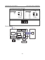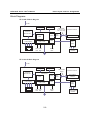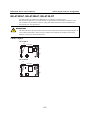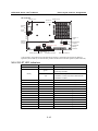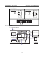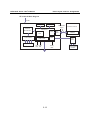
1
NE-4100-P Series User’s Manual First Edition, September 2006 www.moxa.com/product MOXA Technologies Co., Ltd. Tel: +886-2-8919-1230 Fax: +886-2-8919-1231 Web: www.moxa.com MOXA Technical Support [email protected] Worldwide: [email protected] The Americas NE-4100-P Series User’s Manual The software described in this manual is furnished under a license agreement and may be used only in accordance with the terms of that agreement. Copyright Notice Copyright © 2006 MOXA Technologies Co., Ltd. All rights reserved. Reproduction without permission is prohibited. Trademarks MOXA is a registered trademark of The MOXA Group. All other trademarks or registered marks in this manual belong to their respective manufacturers. Disclaimer Information in this document is subject to change without notice and does not represent a commitment on the part of MOXA. MOXA provides this document “as is,” without warranty of any kind, either expressed or implied, including, but not limited to, its particular purpose. MOXA reserves the right to make improvements and/or changes to this manual, or to the products and/or the programs described in this manual, at any time. Information provided in this manual is intended to be accurate and reliable. However, MOXA assumes no responsibility for its use or for any infringements on the rights of third parties that may result from its use. This product may include unintentional technical or typographical errors. Changes are periodically made to the information herein to correct such errors, and these changes are incorporated into new editions of the publication. Table of Contents Chapter 1. Introduction ...............................................................................................1-1 Overview .............................................................................................................................. 1-2 Package Checklist................................................................................................................. 1-2 Product Features ................................................................................................................... 1-2 Product Specifications .......................................................................................................... 1-3 Chapter 2. Panel Layout and Pin Assignments ........................................................2-1 NE-4100T-P, NE-4100-ST.................................................................................................... 2-2 Panel Layout................................................................................................................. 2-2 NE-4100-ST LED Indicators ........................................................................................ 2-2 Pin Assignments ........................................................................................................... 2-3 Block Diagrams ............................................................................................................ 2-4 NE-4110S-P, NE-4110A-P, NE-4110-ST.............................................................................. 2-5 Panel Layout................................................................................................................. 2-5 NE-4110-ST LED Indicators ........................................................................................ 2-6 Pin Assignments ........................................................................................................... 2-6 Block Diagrams ............................................................................................................ 2-8 NE-4120S-P, NE-4120A-P, NE-4120-ST ............................................................................. 2-9 Panel Layout................................................................................................................. 2-9 NE-4120-ST LED Indicators ...................................................................................... 2-10 Pin Assignments ......................................................................................................... 2-11 Block Diagrams .......................................................................................................... 2-12 Chapter 3. Getting Started ..........................................................................................3-1 Wiring Precautions ............................................................................................................... 3-2 Installing the NE-4100T-P onto the NE-4100-ST................................................................. 3-3 Installing the NE-4110S-P, NE-4110A-P onto the NE-4110-ST........................................... 3-3 Installing the NE-4120S-P, NE-4120A-P onto the NE-4120-ST .......................................... 3-4 Selecting the Serial Interface................................................................................................ 3-4 Circuit Pad for External Connection..................................................................................... 3-5 Connecting the Power........................................................................................................... 3-5 Connecting to the Network................................................................................................... 3-6 Connecting to a Serial Device .............................................................................................. 3-6 Digital I/O Channel Settings................................................................................................. 3-6 Digital Output LED Circuit Design .............................................................................. 3-8 Appendix A. Well Known Port Numbers ...................................................................... A-1 Appendix B. Service Information.................................................................................. B-1 MOXA Internet Services ......................................................................................................B-2 Problem Report Form ...........................................................................................................B-3 Product Return Procedure.....................................................................................................B-4 1 Chapter 1. Introduction The NE-4100-P Series embedded device server is a line of compact programmable modules that act as network enablers. NE-4100-P Series modules can be installed in or on a serial device to connect it to an Ethernet network, allowing you to gain network access to any electronic device that has a serial port. All NE-4100-P Series modules come equipped with built-in TCP/IP protocols for fast integration, saving you time and energy on programming. The following topics are covered in this chapter. Overview Package Checklist Product Features Product Specifications NE-4100-P Series User’s Manual Introduction Overview NE-4100-P Series modules are a type of embedded device server or network enabler. The module may be installed in or attached to a serial device to make it accessible from a network. There are three types of module offered: drop-in (NE-4100T-P), RJ45 (NE-4110S-P, NE-4110A-P), and pin header (NE-4120S-P, NE-4120A-P). The last two letters of the model number indicates the serial signal supported by the module. T-P indicates a TTL connector, S-P indicates an RS-232 connector, and A-P indicates an RS-422/485 connector. Each module includes 4 digital input/output channels, also known as DIO channels or GPIO channels. NE-4100-P Series modules are very compact—less than half the size of a credit card. At such a small size, they can be installed into almost any serial device. Each NE-4100-P Series module also comes with a built-in TCP/IP stack for fast integration. Engineers can spend less time on TCP/IP programming, and focus more on developing other major features, thereby shortening your product’s time to market. In addition, a Windows-based NECI (Network Enabler Configuration Interface) library is available to help you develop your own Windows utilities. Each module comes with a complete development kit containing an evaluation board, documents, sample code, cables, and accessories. Package Checklist z z z z z z z z z 1 NE-4100-P Series module 1 NE-4100-ST (the evaluation board) NE-4100-P Series documentation & software CD 1 universal power adaptor 2 power cords 1 null modem cable 1 cross-over Ethernet cable Warranty statement Quick Installation Guide NOTE: Please notify your sales representative if any of the above items is missing or damaged. Product Features All NE-4100-P Series modules have the following features: z z z z z z 10/100 Mbps auto-sensing Ethernet interface Compact size and ready-to-go design (NE-4100T-P measures 45 × 36 mm, other models measure 57 × 40 mm) Built-in TCP/IP firmware for fast integration Low power consumption (1.5W) 4 dedicated digital input/output (DIO) channels for user applications Software reset 1-2 NE-4100-P Series User’s Manual Introduction Product Specifications NE-4100T-P NE-4110S-P, NE-4110A-P NE-4120S-P, NE-4120A-P System CPU 16-bit MCU RAM 1 MB Flash 2 MB LAN Ethernet 10/100 Mbps, pin headers Protection 10/100 Mbps, RJ45 10/100 Mbps, pin headers built-in transformer with 1.5 KV magnetic isolation Serial Interface TTL Port Type pin header RS-232 (NE-4110S-P) RS-232 (NE-4120S-P) RS-422/485 (NE-4110A-P) RS-422/485 (NE-4120A-P) RJ45 pin header TTL, RS-232: TxD, RxD, RTS, CTS, DTR, DSR, DCD, GND RS-422: TxD+, TxD-, RxD+, RxD-, GND RS-485 (2-wire): Data+, Data-, GND RS-485 (4-wire): TxD+, TxD-, RxD+, RxD-, GND Signals Serial Communication Parameters Parity None, Even, Odd, Space, Mark Data Bits 5, 6, 7, 8 Stop Bit 1, 1.5, 2 Flow Control RTS/CTS, XON/XOFF Transmission Speed 50 bps to 115.2 Kbps for PCB V1.x, 110 bps to 230.4 Kbps for PCB V2.x Software Features Protocols ICMP, ARP, IP, TCP, UDP, DHCP Power Requirements Power Input 5 VDC Power Consumption 290 mA @ 5 VDC (Max.) Environmental Operating Temperature Storage Temperature 0°C to 70°C (32°F to 158°F), 5% to 95%RH -20°C to 85°C (-4°F to 185°F), 5% to 95%RH Regulatory Approvals EMC FCC Class A, CE Class A Warranty 5 years 1-3 2 Panel Layout and Pin Assignments Chapter 2. This chapter includes information about the panel layouts and pin assignments for NE-4100-P Series modules. The layouts and reference circuit diagrams for the evaluation boards are also covered. The evaluation boards are used for evaluation and development of applications for NE-4100-P Series modules. The following topics are covered in this chapter: NE-4100T-P, NE-4100-ST ¾ ¾ ¾ ¾ NE-4100-ST LED Indicators Pin Assignments Block Diagrams NE-4110S-P, NE-4110A-P, NE-4110-ST ¾ ¾ ¾ ¾ Panel Layout Panel Layout NE-4110-ST LED Indicators Pin Assignments Block Diagrams NE-4120S-P, NE-4120A-P, NE-4120-ST ¾ ¾ ¾ ¾ Panel Layout NE-4120-ST LED Indicators Pin Assignments Block Diagrams NE-4100-P Series User’s Manual Panel Layout and Pin Assignments NE-4100T-P, NE-4100-ST The NE-4100T-P is a TTL-to-Ethernet drop-in module. It measures 45 × 36 mm, and has a dual-in-line, 26-pin design, making it easy to integrate with your serial devices. The NE-4100-ST is the evaluation board for testing NE-4100T-P modules and developing your own applications. Panel Layout NE-4100T-P Pin #1 45.00 mm 36.00 mm Pin #14 NE-4100-ST 149.00 mm Ethernet Port 99.00 mm Power Jack DI/O Selector Jumpers ON 1 DIP 2 3 4 DI/O Signal Setting Switches Reset Button Debug Serial COM Port Serial Port (RS-232) DI/O Terminal Block NE-4100-ST LED Indicators LED Name Power LED Color red green Ready steady off DIO0 DIO1 DIO2 red red red 2-2 LED Function Indicates the power is on. Power is on and NE-4100T-P is Steady on: functioning normally. y Power is off, or power error condition exists. y IP address cannot be found in DHCP mode. y IP address conflict. Indicates that DIO is in “low” (0) status. Indicates that DIO is in “low” (0) status. Indicates that DIO is in “low” (0) status. NE-4100-P Series User’s Manual LED Name DIO3 TXD0 RXD0 DTR0 CTS0 DSR0 DCD0 RTS0 TXD1 RXD1 Panel Layout and Pin Assignments LED Color red red red red red red red red red red LED Function Indicates that DIO is in “low” (0) status. Indicates that TXD0 has a signal. Indicates that RXD0 has a signal. Indicates that DTR0 has a signal. Indicates that CTS0 has a signal. Indicates that DSR0 has a signal. Indicates that DCD0 has a signal. Indicates that RTS0 has a signal. Indicates that TXD1 has a signal. Indicates that RXD1 has a signal. Pin Assignments NE-4100T-P Pin 1 2 3 4 5 6 7 8 9 10 11 12 13 Signal ETx+ ETxERx+ ERx10M LED TXD RXD RTS CTS Reset GND GND TXD1* Pin 14 15 16 17 18 19 20 21 22 23 24 25 26 Signal PIO0 PIO1 PIO2 PIO3 100M LED DCD DSR DTR GND Ready LED +5V +5V RXD1* *Pins 13 and 26 control the NE-4100-ST Debug Serial COM Port’s TXD and RXD signals. The location of the Debug Serial COM Port is shown on the previous page. This port is not used with NE-4100-P Series modules. ATTENTION NE-4100T-P Ethernet Signals: ETx+, ETx-, ERx+, ERx- Serial Signals: TXD, RXD, RTS, CTS, DCD, DSR, DTR LED Controls: 10M LED, 100M LED, Ready LED 2-3 NE-4100-P Series User’s Manual Panel Layout and Pin Assignments NE-4100-ST Serial Port Pinouts (DB9 Male) Debug Serial Port (reserved) Pin Signal 2 3 5 RXD TXD GND RS-232 Port for Connecting Serial Devices Pin Signal 1 2 3 4 5 6 7 8 DCD RXD TXD DTR GND DSR RTS CTS 5 3 2 5 4 3 2 1 DIO Terminal Block D0 D1 D2 D3 Block Diagrams +5 VDC 1 MB SDRAM Customer's Device 2 MB Flash 80186 CPU 10/100M Ethernet PHY TTL Serial data UART0 (Tx, Rx, RTS, CTS, DTR, DSR, DCD) MAC Transformer 1.5 KV Isolation GPIO Port PIO0 - PIO3 10M 100M LED LED RJ45 Ready LED UART1 Line Driver Tx Rx Serial Console interface 2-4 UART 8 7 6 NE-4100-P Series User’s Manual Panel Layout and Pin Assignments NE-4110S-P, NE-4110A-P, NE-4110-ST The NE-4110S-P is an RS-232-to-Ethernet server, and the NE-4110A-P is an RS-422/485-to-Ethernet server. Both models use an RJ45 connection and measure 57 × 40 mm. The NE-4110-ST is the evaluation board for testing NE-4110S-P and NE-4110A-P modules and developing your own applications. Panel Layout NE-4110S-P 1 2 57.00 mm 2 10 1 9 40.00 mm J1 14 13 J2 NE-4110A-P 1 2 57.00 mm 2 10 1 9 40.00 mm JP2 J1 14 13 J2 NE-4110-ST 149.00 mm 1 2 Jumper 9 (J9) 9 10 1 2 Power Jack 99.00 mm 13 14 Jumper 10 (J10) Interface Selector Jumpers ON 1 DIP 2 3 4 DI/O Selector Jumpers DI/O Signal Setting Switches Reset Button Debug Serial COM Port Serial Port (RS-232) DI/O Terminal Block * JP2 is used to select RS-232 or RS-422/485 operation. Use the RS-232 position for RS-232 operation (NE-4110S-P); use the RS-485 position for RS-422 or RS-485 operation (NE-4110A-P). 2-5 NE-4100-P Series User’s Manual Panel Layout and Pin Assignments NE-4110-ST LED Indicators LED Name Power LED Color red green Ready steady off DIO0 DIO1 DIO2 DIO3 TXD0 RXD0 DTR0 CTS0 DSR0 DCD0 RTS0 TXD1 RXD1 red red red red red red red red red red red red red LED Function Indicates the power is on. Steady on: Power is on and NE-4110 is functioning normally. y Power is off, or power error condition exists. y IP address cannot be found in DHCP mode. y IP address conflict. Indicates that DIO is in “low” (0) status. Indicates that DIO is in “low” (0) status. Indicates that DIO is in “low” (0) status. Indicates that DIO is in “low” (0) status. Indicates that TXD0 has a signal. Indicates that RXD0 has a signal. Indicates that DTR0 has a signal. Indicates that CTS0 has a signal. Indicates that DSR0 has a signal. Indicates that DCD0 has a signal. Indicates that RTS0 has a signal. Indicates that TXD1 has a signal. Indicates that RXD1 has a signal. Pin Assignments NE-4110S-P Serial Header Pinouts (J1) NC CTS0 DSR0 DTR0 RxD0 10 8 6 4 2 9 7 5 3 1 NC RTS0 GND TxD0 DCD0 NE-4110A-P Serial Header Pinouts (J1) NC NC NC RxDTxD+ 10 8 6 4 2 9 7 5 3 1 NC NC GND RxD+ TxD- ATTENTION The symbols “B” and “A” are often used in place of “+” and “-”, respectively. ATTENTION For the 2-wire RS-485 interface, pin 3 is for Data+ (B) and pin 4 is for Data- (A). 2-6 NE-4100-P Series User’s Manual Panel Layout and Pin Assignments NE-4110S-P and NE-4110A-P Ethernet Port Pinouts Pin Signal 1 2 3 6 Tx+ TxRx+ Rx- 1 8 RJ45 Port NE-4110S-P and NE-4110A-P DIO and LED Header Pinouts (J2) GND GND DIO0 DIO1 DIO2 DIO3 TxD1 14 12 10 8 6 4 2 13 11 9 7 5 3 1 VCC(+5V) VCC(+5V) 10M_LED 100M_LED Ready_LED Reset RxD1 NE-4110-ST Pinouts Debug Serial Port (reserved) Pin Signal 2 3 5 RXD TXD GND 5 3 2 RS-232 Port for Serial Devices Pin Signal 1 2 3 4 5 6 7 8 DCD RXD TXD DTR GND DSR RTS CTS Serial and DIO Terminal Blocks TXD+ TXD- RXD+ RXD- SGND Data+ Data- 2-7 D0 D1 D2 D3 5 4 3 2 1 8 7 6 NE-4100-P Series User’s Manual Panel Layout and Pin Assignments Block Diagrams NE-4110S-P Block Diagram +5 VDC 1 MB SDRAM 2 MB Flash Serial data (Tx, Rx, RTS, CTS, DTR, DSR, DCD) 10/100 M Ethernet PHY 80186 CPU UART0 MAC Transformer 1.5 KV isolation Customer's device GPIO Port PIO0 - PIO3 Line Driver RS-232 interface UART1 Line Driver Tx+ Tx- Rx+ Rx- 1 Tx 8 10M 100M LED LED RJ45 Ready LED Rx Serial console interface NE-4110A-P Block Diagram +5 VDC 1 MB SDRAM 2 MB Flash RS-422/485 Signal 10/100 M Ethernet PHY 80186 CPU UART0 MAC Transformer 1.5 KV isolation Customer's device GPIO Port PIO0 - PIO3 Line Driver RS-422/485 interface UART1 Line Driver Tx+ Tx- Rx+ Rx- 1 Tx 8 RJ45 10M 100M LED LED Ready LED 2-8 Rx Serial console interface NE-4100-P Series User’s Manual Panel Layout and Pin Assignments NE-4120S-P, NE-4120A-P, NE-4120-ST The NE-4120S-P is an RS-232-to-Ethernet server, and the NE-4120A-P is an RS-422/485-to-Ethernet server. Both models use pin headers instead of RJ45 connectors. The NE-4120-ST is the evaluation board for testing NE-4120S-P and NE-4120A-P modules and developing your own applications. ATTENTION The NE-4120-ST is the same board as the NE-4110-ST but with an RJ45 jack and pin headers. If your evaluation board has “NE-4110-ST” printed on the board but has the RJ45 jack and pin headers, you have the NE-4120-ST board. Panel Layout NE-4120S-P J3 1 2 57.00 mm 4 1 9 2 10 5 3 2 1 40.00 mm J1 14 13 J2 NE-4120A-P J3 J1 2 10 1 9 5 4 3 2 1 14 J2 13 40.00 mm JP2 1 2 57.00 mm 2-9 NE-4100-P Series User’s Manual Panel Layout and Pin Assignments NE-4120-ST Jumper 7 (J7) Jumper 9 (J9) 149.00 mm 1 2 Ethernet Port 5 3 3 9 10 1 2 2 Power Jack 1 99.00 mm 13 14 Jumper 10 (J10) Interface Selector Jumpers ON 1 DIP 2 3 4 DI/O Selector Jumpers DI/O Signal Setting Switches Reset Button Debug Serial COM Port Serial Port (RS-232) DI/O Terminal Block * JP2 is used to select RS-232 or RS-422/485 operation. Use the RS-232 position for RS-232 operation (NE-4120S-P); use the RS-485 position for RS-422 or RS-485 operation (NE-4120A-P). NE-4120-ST LED Indicators LED Name Power LED Color red green Ready off DIO0 DIO1 DIO2 DIO3 TXD0 RXD0 DTR0 CTS0 DSR0 DCD0 RTS0 TXD1 RXD1 red red red red red red red red red red red red red 2-10 LED Function Indicates the power is on. Steady on: Power is on and NE-4120 is functioning normally. y Power is off, or power error condition exists. y IP address cannot be found in DHCP mode. y IP address conflict. Indicates that DIO is in “low” (0) status. Indicates that DIO is in “low” (0) status. Indicates that DIO is in “low” (0) status. Indicates that DIO is in “low” (0) status. Indicates that TXD0 has a signal. Indicates that RXD0 has a signal. Indicates that DTR0 has a signal. Indicates that CTS0 has a signal. Indicates that DSR0 has a signal. Indicates that DCD0 has a signal. Indicates that RTS0 has a signal. Indicates that TXD1 has a signal. Indicates that RXD1 has a signal. NE-4100-P Series User’s Manual Panel Layout and Pin Assignments Pin Assignments NE-4120S-P Serial Header Pinouts (J1) NC CTS0 DSR0 DTR0 RxD0 10 8 6 4 2 9 7 5 3 1 NC RTS0 GND TxD0 DCD0 NE-4120A-P Serial Header Pinouts (J1) NC NC NC RxDTxD+ 10 8 6 4 2 9 7 5 3 1 NC NC GND RxD+ TxD- ATTENTION The symbols “B” and “A” are often used in place of “+” and “-”, respectively. ATTENTION For the 2-wire RS-485 interface, pin 3 is for Data+ (B) and pin 4 is for Data- (A). NE-4120S-P and NE-4120A-P Ethernet Header Pinouts (J3) Tx+ 1 Tx- 2 3 Rx+ Rx- 4 5 NE-4120S-P and NE-4120A-P DIO and LED Header Pinouts (J2) GND GND DIO0 DIO1 DIO2 DIO3 TxD1 14 12 10 8 6 4 2 13 11 9 7 5 3 1 VCC(+5V) VCC(+5V) 10M_LED 100M_LED Ready_LED Reset RxD1 2-11 NE-4100-P Series User’s Manual Panel Layout and Pin Assignments NE-4120-ST Pinouts Debug Serial Port (reserved) Pin Signal 2 3 5 RXD TXD GND RS-232 Port for Serial Devices 5 3 2 Pin Signal 1 2 3 4 5 6 7 8 DCD RXD TXD DTR GND DSR RTS CTS 5 4 3 2 1 8 7 6 Serial and DIO Terminal Blocks TXD+ TXD- RXD+ RXD- SGND D0 D1 D2 D3 Data+ Data- Block Diagrams NE-4120S-P Block Diagram +5 VDC 1 MB SDRAM 2 MB Flash Serial data (Tx, Rx, RTS, CTS, DTR, DSR, DCD) 10/100 M Ethernet PHY 80186 CPU UART0 MAC Transformer 1.5 KV isolation Customer's device GPIO Port PIO0 - PIO3 Line Driver RS-232 interface UART1 Line Driver Tx+ Tx- Rx+ Rx- Pin header Tx 10M 100M LED LED Ready LED 2-12 Rx Serial console interface NE-4100-P Series User’s Manual Panel Layout and Pin Assignments NE-4120A-P Block Diagram +5 VDC 1 MB SDRAM 2 MB Flash RS-422/485 Signal 10/100 M Ethernet PHY 80186 CPU UART0 MAC Transformer 1.5 KV isolation Customer's device GPIO Port PIO0 - PIO3 Line Driver RS-422/485 interface UART1 Line Driver Tx+ Tx- Rx+ Rx- Pin header Tx 10M 100M LED LED Ready LED 2-13 Rx Serial console interface 3 Chapter 3. Getting Started This chapter includes information about installation of NE-4100-P Series modules for development and testing. The following topics are covered in this chapter: Wiring Precautions Installing the NE-4100T-P onto the NE-4100-ST Installing the NE-4110S-P, NE-4110A-P onto the NE-4110-ST Installing the NE-4120S-P, NE-4120A-P onto the NE-4120-ST Selecting the Serial Interface Circuit Pad for External Connection Connecting the Power Connecting to the Network Connecting to a Serial Device Digital I/O Channel Settings ¾ Digital Output LED Circuit Design NE-4100-P Series User’s Manual Getting Started Wiring Precautions This section describes some important safety precautions that you should pay attention to before proceeding with any installation. ATTENTION Be sure to disconnect the power cord before installing or wiring the evaluation board. ATTENTION Determine the maximum possible current in each power wire and common wire. Observe all electrical codes dictating the maximum current allowable for each wire size. If the current goes above the maximum ratings, the wiring could overheat, causing serious damage to your equipment. ATTENTION Please take care when handling the evaluation board. When plugged in, the board’s internal components generate heat, and consequently the board may feel hot to the touch. You should also pay attention to the following: z z z z Do not run signal or communication wiring and power wiring in the same wire conduit. To avoid interference, wires with different signal characteristics should be routed separately. Separate paths should be used to route wiring for power and devices. You can use the type of signal transmitted through a wire to determine which wires should be kept separate. The rule of thumb is that wires sharing similar electrical characteristics may be bundled together. Keep input wiring and output wiring separate. If power wiring and device wiring paths must cross paths, make sure the wires are perpendicular at the intersection point. All wiring should be clearly labeled. 3-2 NE-4100-P Series User’s Manual Getting Started Installing the NE-4100T-P onto the NE-4100-ST Before using the NE-4100-ST evaluation board with the module, disconnect the power supply, network, and serial device. In the center of the evaluation board, there is a square with one white inverted triangle (shown as black in the figure) on one of its sides, and 2 rows of female sockets on the other two sides. The NE-4100T-P module also has a white inverted triangle on one of its sides. When attaching the module to the evaluation board, make sure these 2 white inverted triangles are facing the same direction, as shown in the following figure. After the module is installed, connect the power supply, network, and serial device to the evaluation board. NE-4100-ST Starter Kit NE-4100T Series Module ON 1 DIP 2 3 4 Installing the NE-4110S-P, NE-4110A-P onto the NE-4110-ST The NE-4110S-P and NE -4110A-P modules are attached to the NE-4110-ST board using mounting screws that are provided with the board. When attaching the module to the board, make sure that the module is oriented so that the jumper banks on the module and the board are aligned as shown below. Use the provided ribbon cables to connect jumper block J1 on the module to J9 on the board, and jumper block J2 on the module to J10 on the board. When plugging in each ribbon cable, make sure that the red key wire corresponds with pin 1 on each jumper block. J1 J9 1 2 NE-4110-ST Starter Kit 2 10 1 9 1 2 9 10 1 2 J2 14 13 NE-4110 Series Module 13 14 J10 ON 1 3-3 DIP 2 3 4 NE-4100-P Series User’s Manual Getting Started Installing the NE-4120S-P, NE-4120A-P onto the NE-4120-ST The NE-4120S-P and NE -4120A-P modules are attached to the NE-4120-ST board using mounting screws that are provided with the board. When attaching the module to the board, make sure that the module is oriented so that the jumper banks on the module and the board are aligned as shown below. Use the provided ribbon cables to connect jumper block J1 on the module to J9 on the board, J2 on the module to J10 on the board, and J3 on the module to J7 on the board. When plugging in each ribbon cable, make sure that the red key wire corresponds with pin 1 on each jumper block. J1 J9 1 2 NE-4120-ST Starter Kit 1 2 5 2 10 1 9 4 9 10 1 2 3 5 2 4 1 3 2 1 J7 J3 J2 14 13 NE-4120 Series Module 13 14 J10 ON 1 DIP 2 3 4 Selecting the Serial Interface NE-4100-P Series modules are available for different serial interfaces. The NE-4110S-P and NE-4120S-P are designed for the RS-232 interface, and the NE-4110A-P and NE-4120A-P are designed for the RS-422/485 interface. On the NE-4110-ST and NE-4120-ST evaluation boards, the Network Enabler Interface jumper block is used to select the serial interface used for your particular module. For the NE-4110S-P and NE-4120S-P, the evaluation board should be configured for the RS-232 interface, as shown below. JP2 Network Enabler Interface RS485 RS232 For the NE-4110A-P and NE-4120A-P, the evaluation board should be configured for the RS-485 interface, as shown below. JP2 Network Enabler Interface RS485 RS232 3-4 NE-4100-P Series User’s Manual Getting Started Note that the RS-485 interface is selected on the evaluation board for the NE-4110A-P and NE-4120A-P modules, even when the module is operating in RS-422 mode. Please refer to Chapter 2 - Panel Layout and Pin Assignments for additional details. Circuit Pad for External Connection A circuit pad is provided on the right side of each evaluation board for the development of additional application circuits. 5V 3.3V 1 2 1 2 J3 J9 9 10 9 10 1 2 1 2 J4 J10 13 14 13 14 GND ON 1 DIP 2 3 4 The first row of the circuit pad is for connecting a 5V power supply; the second row is for connecting a 3.3V power supply. The last row of the circuit pad is for grounding. Serial signals are mapped to J3 as an extension of jumper block J9. DIO and LED signals are mapped to J4 as an extension of jumper block J10. This means that pin assignments for J3 on the circuit pad are the same as the pin assignments for jumper block J9; pin assignments for J4 on the circuit pad are the same as the pin assignments for jumper block J10. 5V 3.3V 1 2 1 2 J3 J9 9 10 9 10 1 2 1 2 J4 J10 13 14 13 14 GND Connecting the Power Connect the 12 VDC power line with the evaluation board’s power jack. If the power is properly supplied, the power LED will show a solid red color until the system is ready, at which time the ready LED will show a solid green color. 3-5 NE-4100-P Series User’s Manual Getting Started Connecting to the Network To connect to the network for testing and development purposes, the module should be installed onto its evaluation board. Make sure that the module is correctly installed onto the evaluation board, then plug the Ethernet cable into the RJ45 jack. For models NE-4100T-P, NE-4120S-P, and NE-4120A-P, the RJ45 jack is located on the evaluation board; for models NE-4110S-P and NE-4110A-P, the RJ45 jack is located on the module itself. If the cable is properly connected, the RJ45 connector will indicate a valid connection to the Ethernet as follows: LAN LAN The green LED in the upper right corner blinks when the cable is properly connected to a 100 Mbps Ethernet network, and data is being transmitted. The yellow LED in the upper left corner blinks when the cable is properly connected to a 10 Mbps Ethernet network, and data is being transmitted. When using a private IP address for the module, which is the factory default, make sure that netmask and IP settings are configured appropriately in order to access the module from a host on the network. Connecting to a Serial Device To connect to a serial device for testing and development purposes, the module should be installed onto its evaluation board. The module’s serial signals are routed to and from the RS-232 COM port on the evaluation board Use a serial data cable to connect the serial device to the COM port on the evaluation board. Digital I/O Channel Settings Each module provides 4 digital I/O (DIO) channels. All 4 DIO channels may be configured by software for either digital output or digital input mode. A DI channel is a channel that is operating in digital input mode; a DO channel is a channel that is operating in digital output mode. You may use the evaluation board’s Digital Output LEDs and Digital Input DIP switches as the digital input and output devices, or you may connect digital input/output devices to the DI/O Terminal Block. ATTENTION When using a digital input device connected to the DI/O Terminal Block, the corresponding Digital Input DIP switch must be set to “OFF” or “High”. Setting the DIP switch to “ON” or “Low” will interfere with the signal from your digital input device. 3-6 NE-4100-P Series User’s Manual Getting Started DI/O Selectable Jumper DI/O Mode DI DO 0 1 2 3 Digital Input 0 1 2 3 ON 1 DIP 2 3 ON: Low OFF: High Digital Input Signal Setting Switch 4 Digital Output DO0 DO1 DO2 DO3 Digital Output LEDs : Low : High DO0 DO1 DO2 DO3 DI/O Terminal Block DI/O Mode jumpers 0 through 3 correspond with DIO channels 0 through 3. The jumper’s position determines whether the corresponding channel is linked to a DIP switches or to an LED. When a channel’s jumper is set to the DI position, the channel’s input signal is controlled by the corresponding Digital Input DIP switch. When the jumper is set to the DO position, the channel’s output signal is routed to the corresponding Digital Output LED. For example, if DIO channel 0 is operating as a digital input channel, setting DI/O Mode jumper 0 to the DI position enables the use of DIP switch 0 as that channel’s input device. DI/O Mode DI DO 0 1 2 3 ATTENTION The DI/O Mode jumpers are used to tell the evaluation board whether to use the Digital Output LEDs or the Digital Input DIP switches. The jumpers do not control the channel’s mode. Input and output mode is configured through the web, serial, or Telnet console, or through Network Enabler Administrator. When using a Digital Input DIP switch as your input device, the “ON” position corresponds to “Low” status and the “OFF” position corresponds to “High” status. The result can be monitored with the Network Enabler Administrator or with the web console. Make sure all DIP switches are set to “OFF” if you are using your own digital input device that is connected to the evaluation board’s terminal block. Digital Input 0 1 ON 2 3 DIP ON: Low OFF: High 1 2 3 4 3-7 NE-4100-P Series User’s Manual Getting Started For channels in digital output mode, “Low” and “High” status is controlled from within the web console. When using a Digital Output LED as your output device, “Low” status will be expressed by the LED lighting up, and “High” status will be expressed by the LED turning off. Digital Output DO0 DO1 DO2 DO3 : Low : High Digital Output LEDs Digital Output LED Circuit Design The figure shown below is the digital output LED circuit design. This is known as the “sink” design. Dout 3.3V When developing your own applications, you need to be aware of the voltage limits shown below. Min. Low-level Input Voltage High-level Input Voltage Low-level Input Voltage High-level Input Voltage Maximum voltage when DI is set to “Low” status. ----Minimum voltage when DI is set to “High” status. 0.7xVCC Maximum voltage when DO is set to “Low” status. ----Minimum voltage when DO is set to “High” status 2.4 Max. 0.3xVCC V ----- V 0.4 V ----- V The output current for digital output channels carries only 1 mA. 3-8 Unit Conditions A Appendix A. Well Known Port Numbers This appendix is included for your reference. Listed below are port numbers that already have a well-established use. These port numbers should be avoided when assigning a port number to your NE-4100-P Series module; otherwise you may experience network problems. Refer to the RFC 1700 standard for Well Known Port Numbers or refer to the following introduction from IANA. The port numbers are divided into three ranges: the Well Known Ports, the Registered Ports, and the Dynamic and/or Private Ports. The Well Known Ports are those from 0 through 1023. The Registered Ports are those from 1024 through 49151. The Dynamic and/or Private Ports are those from 49152 through 65535. The Well Known Ports are assigned by IANA, and on most systems, can only be used by system processes or by programs executed by privileged users. The following table shows famous port numbers among the well-known port numbers. For more details, please visit the IANA website at http://www.iana.org/assignments/port-numbers. TCP Socket Application Service 0 reserved 1 TCP Port Service Multiplexor 2 Management Utility 7 Echo 9 Discard 11 Active Users (systat) 13 Daytime 15 Netstat 20 FTP data port 21 FTP CONTROL port 23 Telnet 25 SMTP (Simple Mail Transfer Protocol) 37 Time (Time Server) 42 Host name server (names server) NE-4100-P Series User’s Manual Well Known Port Numbers TCP Socket Application Service 43 Whois (nickname) 49 (Login Host Protocol) (Login) 53 Domain Name Server (domain) 79 Finger protocol (Finger) 80 World Wide Web HTTP 119 Network News Transfer Protocol (NNTP) 123 Network Time Protocol 213 IPX 160 – 223 Reserved for future use UDP Socket Application Service 0 reserved 2 Management Utility 7 Echo 9 Discard 11 Active Users (systat) 13 Daytime 35 Any private printer server 39 Resource Location Protocol 42 Host name server (names server) 43 Whois (nickname) 49 (Login Host Protocol) (Login) 53 Domain Name Server (domain) 69 Trivial Transfer Protocol (TETP) 70 Gopler Protocol 79 Finger Protocol 80 World Wide Web HTTP 107 Remote Telnet Service 111 Sun Remote Procedure Call (Sunrpc) 119 Network news Tcanster Protocol (NNTP) 123 Network Time protocol (nnp) 161 SNMP (Simple Network Mail Protocol) 162 SNMP Traps 213 IPX (Used for IP Tunneling) A-2 B Appendix B. Service Information This appendix contains information on how to obtain information or service from MOXA for your NE-4100-P Series embedded device server and other MOXA products. The following topics are covered: MOXA Internet Services ¾ ¾ Technical support e-mail address Website for product information Problem Report Form Product Return Procedure NE-4100-P Series User’s Manual Service Information MOXA Internet Services Customer satisfaction is our top priority. To ensure that customers receive the full benefit of our products, MOXA Internet Services has been set up to provide technical support, driver updates, product information, and user’s manual updates. The following services are provided: Technical support e-mail address [email protected] Website for product information http://www.moxa.com B-2 NE-4100-P Series User’s Manual Service Information Problem Report Form MOXA NE-4100 Series Embedded Device Server Customer name: Company: Tel: Fax: Email: Date: Select Product Model NE-4100T NE-4110S NE-4110A NE-4120S NE-4120A NE-4100T-P NE-4110S-P NE-4110A-P NE-4120S-P NE-4120A-P Serial Number:____________________________________________________________________________ Problem Description Please describe the symptoms of the problem as clearly as possible, including any error messages you see. A clearly written description of the problem will allow us to reproduce the symptoms and expedite the repair of your product. B-3 NE-4100-P Series User’s Manual Service Information Product Return Procedure For product repair, exchange, or refund, the customer must: z z z z Provide evidence of original purchase. Obtain a Product Return Agreement (PRA) from the sales representative or dealer. Fill out the Problem Report Form (PRF). Include as much detail as possible for a shorter product repair time. Carefully pack the product in an anti-static package and send it, pre-paid, to the dealer. The PRA should be visible on the outside of the package and should include a description of the problem along with the return address and telephone number. B-4