1
AL532
Service Manual
TABLE OF CONTENTS
SERVICE WARNING∙∙∙∙∙∙∙∙∙∙∙∙∙∙∙∙∙∙∙∙∙∙∙∙∙∙∙∙∙∙∙∙∙∙∙∙∙∙1
A. IMPORTANT SAFETY INSTRUCTION∙∙∙∙∙∙∙∙∙∙∙∙∙∙∙∙∙∙∙∙∙ 1
B. SPECIFICATIONS∙∙∙∙∙∙∙∙∙∙∙∙∙∙∙∙∙∙∙∙∙∙∙∙∙∙∙∙∙∙∙∙∙∙∙∙∙∙2
C. TIMING CHART∙∙∙∙∙∙∙∙∙∙∙∙∙∙∙∙∙∙∙∙∙∙∙∙∙∙∙∙∙∙∙∙∙∙∙∙∙∙ 3
D. CONTROL LOCATION∙∙∙∙∙∙∙∙∙∙∙∙∙∙∙∙∙∙∙∙∙∙∙∙∙∙∙∙∙∙∙∙∙ 5
E. CONDUCTION VIEW∙∙∙∙∙∙∙∙∙∙∙∙∙∙∙∙∙∙∙∙∙∙∙∙∙∙∙∙∙∙∙∙∙∙∙∙6
F. ADJUSTMENT PROCEDURE∙∙∙∙∙∙∙∙∙∙∙∙∙∙∙∙∙∙∙∙∙∙∙∙∙∙∙∙∙10
G. TROUBLE SHOOTING HINTS∙∙∙∙∙∙∙∙∙∙∙∙∙∙∙∙∙∙∙∙∙∙∙∙∙∙∙11
H. REPLACEMENT PARTS LIST∙∙∙∙∙∙∙∙∙∙∙∙∙∙∙∙∙∙∙∙∙∙∙∙∙∙∙15
I. BLOCK DIAGRAM∙∙∙∙∙∙∙∙∙∙∙∙∙∙∙∙∙∙∙∙∙∙∙∙∙∙∙∙∙∙∙∙∙∙∙∙∙21
J. SCHEMATIC DIAGRAM∙∙∙∙∙∙∙∙∙∙∙∙∙∙∙∙∙∙∙∙∙∙∙∙∙∙∙∙∙∙∙∙22
WARNING
To prevent from fire or shock hazard,do not expose monitor to any rain or any form of water.High voltage is
inside the monitor so please do not remove the back cover of the cabinet if you are not a qualified monitor
engineer.Contact the local dealer or the nearest Acer branch office if you need help.
A. IMPORTANT SAFETY INSTRUCTION
Prior to using this service manual,please ensure that you have carefully followed all the procedures outlined in
the user's manual for this product.
1. Read all of these instructions.
2. Save these instructions.
3. Follow all warnings and instructions a marked on the product.
4. Unplug this product from the wall outlet before cleaning.Do not use liquid cleaners or aerosol
cleaners, use a damp cloth for cleaning.
5. Do not use this product near water.
6. Do not place this product on an unstable cart,stand or tablle.The product may fall,causing serious
damage to the product.
7. Slots and openings in the cabinet and the back or bottom are provided for ventilation,to ensure
reliable operation of the product and to protect it from overheating,those openings must not be
blocked or covered.The openings should never be blocked by placing the product on a bed,sofa, rug,
or other similar surface.This product should not be placed in a built-in installation less proper
ventilation is provided.
8. This products should be operated from the type of power source indicated on the marketin label.
If you are not sure of the type of power available, consult your dealer or local power company
9. This product is equipped with a 3-wire grounding type plug,a plug having a third (grounding)
pin.This plug will only fit into a grounding-type power outlet.This is a safety feature,if you are
unable to insert the plug into the outlet,contact your electrician to replace your obsolete outlet.Do
not defeat the purpose of the grounding-type plug.
10. Do not allow anything to rest on the power cord.Do not locate this product where persons will walk
on the cord.
11. If an extension cord is used with this product,make sure that the total of the ampere ratings on the
product plugged into the extension cord to the waplugged into outlet does not exceed 15 ampere.
12. Never push objects of any kind into this product through cabinet slots as they may touch dangerous
voltage points or short out parts that could result in a risk of fire or electric shock.Never spill liquid
of any kind on the product.
13. Do not attempt to service this product yourself,as opening or removing covers may expose you to
dangerous voltage points or other risks.Refer all servicing to service personnel.
14. Unplug this product from the wall outlet and refer servicing to qualified service personnel under the
following conditions.
a. When the power cord or plug is damaged or frayed.
b. If liquid has been spilled into the product.
c. If the product has been exposed to rain or water.
d. If the product does not operate normally,when the operating instructions are followed.Adjust
only those controls that are covered by the operating instructions since improper adjustment of
other controls may result in damage and will often require extension work by a qualified
technician to restore the product to normal operation.
e. If the product has been dropped or the cabinet has been damaged.
f. If the product exhibits a distinct change in performance,indicating a need for service.
B. SPECIFICATIONS
1. Maximum Resolution
2. Recommend Resolution
3. Synchronization Range
Horizontal
Vertical
4. Active Display Area
5. Dot Pitch
6. Support display colors
7. Contrast Ratio (Typical)
8.Luminance of White
9. Bandwidth
10. User Control
11. OSD Function
12. View Angle
Horizontal
Vertical
13. Power Source
14. Power Consumption
15. Connection Type
16. Input Signal
Video
Sync.
17. Color Temperature
18. Dimension (WxHxD)
19. Monitor Weight
20. Base Operation
Tilt
21. Power Saving
ON
STAND BY
OFF
1024 x 768 @ 75Hz
1024 x 768 @ 60Hz
31 – 60 KHz
56– 75 Hz
304.1mm (H) x 228.1mm (V)
0.297(H) x 0.297(V) mm
16.7M color
500
300cd/m²
80MHz
4 Key Switch
Brightness, Conrast, H-Position, V-Position, H-Size, Phase,
Color Select, Auto, Reset, Language, OSD Adjust, Exit
140 Degrees
120 Degrees
100 – 240 Vac 60 / 50 Hz
36W (max.)
15 Pin D Type
Analog R.G.B. , 0.7Vp-p / 75 Ohms
TTL level,positive or negative polarity
Cool / Warm
418mm x 421mm x 188mm
3.3 Kg
0 / + 15 degree
< 36W
< 5W
< 5W
22. Signal Connector Pin Assignment
Pin No.
23. Audio signal
1. Red
2. Green
3. Blue
4. Ground
5. Self Test
6. Red Ground
7. Green Ground
8. Blue Ground
3.5Φ stereo phone jack
Input Sensitivity : 200mV
2+2W 8Ω Speaker
9. 5VDC
10. Sync. Ground
11. Ground
12. SDA (For DDC)
13. Horizontal Sync.
14. Vertical Sync.
15. SCL (For DDC)
C.TIMING CHART
Video
Back porch
Active display
Front porch
Sync.
Sync-width
Total
VESA
VESA
800X600
800X600
36.000
40.000
37.500
35.156
37.879
26.413
26.667
28.444
26.400
25.422
20.317
20.317
22.222
20.000
6.355
6.356
6.095
6.349
6.222
6.400
(µs)
0.635
0.636
0.762
0.508
0.667
1.000
H-Sync-width
(µs)
3.813
3.813
1.270
2.032
2.000
3.200
H-Back Porch
(µs)
1.906
1.907
4.063
3.810
3.556
2.200
70.1
59.94
72.81
75.0
56.25
60.3
14.267
16.683
13.735
13.333
17.778
16.579
V-Active Display (ms)
12.710
15.253
12.678
12.800
17.067
15.840
V-Blanking
(ms)
1.557
1.430
1.057
0.533
0.711
0.739
V-Front Porch
(ms)
0.413
0.318
0.238
0.027
0.028
0.026
V-Sync-width
(ms)
0.064
0.064
0.079
0.080
0.057
0.106
V-Back Porch
(ms)
1.080
1.049
0.740
0.427
0.626
0.607
H/V Sync. Polarity
- +
- -
- -
- -
+ +
+ +
Interlace
NONE
NONE
NONE
NONE
NONE
NONE
VGA
VGA
VESA
720X400
640X480
640X480
28.325
25.175
31.500
31.472
31.469
37.861
(µs)
31.774
31.778
H-Active Display (µs)
25.419
H-Blanking
(µs)
Front Porch
Preset
Modes
Pixel clock
(MHz)
H-Frequency
(KHz)
H-Total
V-Frequency
(Hz)
V-Total
(ms)
VESA
640X480
31.500
Preset
Modes
VESA
VESA
VESA
VESA
VESA
800X600
800X600
1024X768
1024X768
1024X768
Pixel clock
(MHz)
50.000
49.500
65.000
75.000
78.750
H-Frequency
(KHz)
48.077
46.875
48.363
56.476
60.023
(µs)
20.800
21.333
20.677
17.707
16.660
H-Active Display (µs)
16.000
16.162
15.754
13.563
13.003
H-Blanking
(µs)
4.800
5.172
4.923
4.053
3.657
Front Porch
(µs)
1.120
0.323
0.369
0.320
0.203
H-Sync-width
(µs)
2.400
1.616
2.092
1.813
1.219
H-Back Porch
(µs)
1.280
3.232
2.462
1.920
2.235
V-Frequency
(Hz)
72.2
75.0
60.0
70.1
75.0
V-Total
(ms)
13.853
13.333
16.666
14.272
13.328
V-Active Display (ms)
12.480
12.800
15.880
13.599
12.795
V-Blanking
(ms)
1.373
0.533
0.786
0.673
0.533
V-Front Porch
(ms)
0.770
0.021
0.062
0.053
0.017
V-Sync-width
(ms)
0.125
0.064
0.124
0.106
0.050
V-Back Porch
(ms)
0.478
0.448
0.600
0.513
0.466
H/V Sync. Polarity
+ +
+ +
- -
- -
+ +
Interlace
NONE
NONE
NONE
NONE
NONE
H-Total
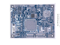
E. CONDUCTION VIEW
MAIN BOARD (Component Side)
MAIN BOARD (Solid Side)
CONTROL BOARD (Component Side)
CONTROL BOARD (Solid Side)
F. ADJUSTMENT PROCEDURE
ITEM
Program Menu.
B+
Check
A
﹟Test Meter
﹡Test Point
﹫Pattern
﹟Digital Voltmeter
﹡CN7
﹫Crosshatch Pattern
(31.5KHz,640x480)
Operation
1. Plug power cable into the adapter, check adapter
power indicator light up green.
2. Make sure the voltage of the power plug (CN7)
on the main PCB to the value shown at right.
Power Saving ﹟Wattmeter
Check
﹟PC or Pattern
B
generator
﹫Crosshatch Pattern
(31.5KHz,640x480)
1. Unplug the signal cable into the monitor.
2. Turn the power switch of the monitor ON.
3. Check monitor power indicator light up orange.
4. Make sure the wattmeter value shown at right.
5. OSD will be display “NO SIGNAL” Picture.
Into Factory ﹟PC or Pattern
mode
generator
C
﹫Crosshatch Pattern
(31.5KHz,640x480)
1. Hold ‹ key,then turn the power switch of the
monitor OFF.
2. Hold › key,then turn the power switch of the
monitor ON.
3. You can into factory adjustment mode.
Check
Value
12.0V
±0.2V
‹ 5W
Auto mode
Check
﹟PC or Pattern
generator
﹫Crosshatch Pattern
(1024x768/60Hz)
1. Press and relese the MENU knob to activate the
OSD menu.
2. Move the OSD to the AUTO function,press MENU
key auto adjuat display mode to its utmost
performance according to VGA setting.
3. In the event of the display image needs further
adjustment
White
Balance
Adjust
﹟PC or Pattern
generator
﹫White Pattern
(1024x768/60Hz)
1. Move the OSD to the COLOR mode (AUTO COLOR). Y = 220
±0.1FL
2. set color is 9300°K using the OSD,Check the value
x = 0.283
shown at below.
±0.01
Y = 220 x = 0.283 y = 0.297
y
=
0.297
3. set color is 6500°K using the OSD,Check the value
±0.01
shown at right.
Y = 220 x = 0.311 y = 0.329
﹟PC or Pattern
generator
1. Move the OSD to the LANGUAGE mode.
2. You can choose one of the eight language you need.
D
E
OSD
F Language
Setting
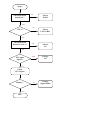
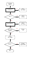
G. TROUBLE SHOOTING HINTS
No Display
( Black )
LED ON ?
NO
NO
Power
adapter ?
YES
Change
adapter
YES
Push the power
ON/OFF switch
LED Color
change ?
YES
Back light
ON?
NO
YES
To Step 2
NO
Check main
board U2/Pin2
Check the CN1/Pin1
of Inverter
Hi / Lo under
push power
sw?
+12V ?
High Voltage !
NO
YES
Make sure the
connection of
Inverter is fine
YES
NO
A
To Step 2
NO
Display ?
Check
F1(Fuse) of inverter
YES
B
OK !
A
B
Check the
connection of
CN8 cable
NO
Change the
main board
Hi / Lo under
push power
sw?
YES
Display ?
YES
NO
Change the
Inverter
OK !
Display ?
Change the
main board
NO
To Step 2
YES
OK !
Step 2
Check the main
board 12V ?
NO
Check
F1,D5
YES
NO
Check
U9,U11,R43
+5.0 V ?
YES
Check the main
board U5 / Pin 3 ?
YES
Check
U5
YES
H/V input
Signal ?
YES
Change
U8
NO
Change
Signal Cable
NO
Check
H/V Signal
Display ?
YES
OK !
No display
(White)
Check the main
board 5V ?
NO
Check
U9,U11,R43
NO
Check
U7,U12
YES
+3.3V ?
YES
Check the main
board U8/Pin1 ?
NO
Check
3.3V Circuit
YES
YES
H/V Input
Signal ?
Change
U8
NO
Check
H/V Signal
Display ?
YES
OK !
NO
Change
Signal Cable
H. REPLACEMENT PARTS LIST
AL532
NO
Parts No.
Description
Part Location
Q’ty
988-1A0-1001C
AS-576 Pcking material+TCO99 SANYO
1
002-001-TCO9
TCO99 Dcclaration
1
002-L01-5EACER
AS576 User’s Manul Acer logo
1
003-101-TCO9
All Series TCO99 Label for Crton
1
005-002-5EACER
AS576 Carton Acer Logo
1
170-000-0848C
PE BAG 0.07mm 14*30.5cm.
1
170-005-LCD5
LCD 15" PE Bag
For DC Line
1
170-005-VM541
LT-541 PE Zipper Bag 300*200mm.
For LCD
1
826-000-AS576
AS-576 Series pcking material
For Manual
1
160-00L-AS576
AS576 Polyfom (L).
1
160-00R-AS576
AS576 Polyfom (R).
1
846-120-C0AL-AT Adapter 12V 3A 36W
1
003-H01-AS576
Acer AL532 TCO99 Label
1
003-401-AS576
Acer AL532 Carton Label
1
002-G00-ACER
NF-787NS warranty card for Europe"Acer”
1
902-AS0-1001C
AS-576 TUV/GS/CE TCO99 Panel
1
151-002-AS576
AS576 Rear cover Acer
1
154-002-ABS6E
Plastic material ABS HB EM-006E
1
110-4R0-20646
Screw M4*H8*Φ6.6mm
2
154-001-AS576
AS576 Key TOP PC
1
123-B02-AS576
AS576"Acer+AL532" logo
1
820-001-5EST
AS576 stand ass’y
1
123-701-AS576
AS576 Base neck AL or ZN.
1
123-700-AS576
AS576 Base AL or ZN.
1
155-001-AS576
Rubber 10*20 Black
4
100-010-4033
Screw P4*10 ISO
600-151-0404
Power cord for Germany 150cm White
1
610-151-15RM-1
SH570/770Signal Cable UL20276 1.5m
1
827-001-AS576
AS-576 LCD Panel Assy material for SANYO
1
100-008-3013
Screw R3*8mm TP1
For Key Top*2
2
100-010-4033
Screw P4*10 ISO
Neck+Hinge*2
2
101-005-2032
Screw M2*5 ISO
Speaker*4
4
101-005-3032
Screw M3.0*5 ISO.
Main PCB*4, Inverter*2
6
103-006-4033
Screw F4*6mm ISO ZI3C
For Rear Cover+Hinge
1
103-010-3012
Screw TAP-BASE.
Panel+Rear Plate*4
4
105-006-3012
Screw T3*6mm TP1.
Control PCB*2
2
105-006-4033-1
Screw T4*6mm ISO
Hinge+Rear Plate*2
2
105-010-3012
SCREW T3*10mm TP1.
Rear Plate+Rear Cabinet*4
4
110-4R0-20646
Screw M4*H8*Φ6.6mm
For Rear Cabinet*2
2
154-002-AS576
AS576 Mylar Sheet T=0.5mm
For Panel C02RD0534
1
BASE+NECK*3
3
506-178-E62BP-40 SMD CPU IC(WINBOND:W78E62BP-40
P1 for U2 ,Socket
1
631-003-A014-C
Audio Cable 3.5Ø STERE0 to 2*RCA connector
631-006-7020-T
SH570/770 1061#28 6P2.0mm
EMI
1
631-008-G020-W
8Pin 1.5Pitch <-> 8Pin 1.5Pitch
CTR/B->M/B
1
631-030-F576
30 PIN FFC Cable L182mm
1
631-040-F576
40 PIN FFC Cable L193mm
1
824-00Q-AY565L
AY565 Speaker Ass'y L
1
154-000-SPCS
AY/CY Series Speaker Case 006 ABS HB
1
710-20A-Y565
AY/CY-565 Speaker (8Ω/1.5W) 40*20mm
1
631-002-904L
CY/AY-565 Speaker Wire 2.0mm pith
1
824-00Q-AY565R
AY565 Speaker Ass'y R
1
154-000-SPCS
AY/CY Series Speaker Case 006 ABS HB
1
710-20A-Y565
AY/CY-565 Speaker (8Ω/1.5W) 40*20mm
1
631-002-902R
HG562A R Speaker Wire 2.0-TIN.
1
154-003-AS576
AS576 Mylar Sheet 168*126mm
1
831-300-0100
Key 粘膠 (5000NS)
1
831-750-0500
Tape 50mm Black
121-000-AS576
Rear Plate SECC 1.0T.
1
126-000-AS576
AS576 Hinge Steelness.
1
600-151-5004-M
Power Cord for UK 150cm White
1
600-151-5504
Power Crd for Swiss 150cm 白色.
1
899-00M-AS576
AS576 Main PCB for SANYO Panel
1
852-00M-AS576
AS576 Main PCB for SANYO Panel SMD
1
200-100-AS576
AS576 Main Board
PCB
1
281-031-20014
SMD RES
R55
1
281-031-62014
SMD RES 6.2K ohm 0603
R46
1
281-035-0R04
SMD RES 0
L12,R21,S1,S2,R13,R14,R63,R64,R65
9
281-035-1014
SMD RES 100 ohm 0603 5%
R42,R44,R45,R82
4
281-035-1024
SMD RES 1K ohm 0603 5%
R6,R7,R24,R29,R30,R31,R33,R37,R73
9
281-035-1034
SMD RES 10k ohm 0603 5%
R2,R8,R9,R15,R34,R35,R36,R48,R61,R70
10
281-035-1054
SMD RES 1M ohm 0603
R53,R17
2
281-035-1514
SMD RES 1M ohm 0603
R12
1
281-035-2034
SMD RES 20K ohm 0603
R56,R59,R78,R80,R84,R87,R88,R90
8
281-035-2224
SMD RES 2.2K ohm 0603
R22,R25,R40,R41,R52,R81,R83
7
281-035-3304
SMD RES 33
R3,R5,R47,R50,R51,L11
6
281-035-3334
SMD RES 33K ohm 0603
R85,R57
2
281-035-4704
SMD RES 47
R72
1
281-035-4724
SMD RES 4.7K ohm 0603
R4,R11,R16,R19,R20,R28,R32,R39
8
281-035-4734
SMD RES 47K ohm 0603
R66,R77
2
281-035-5104
SMD RES 51
R68,R71
2
281-035-5114
SMD RES 510 ohm 0603
R10
1
281-035-7504
SMD RES 75
ohm 0603
R1,R74,R75,R76
4
282-330-2454
SMD RES 33
ohm 1206 ARRAY
RP1,RP4,RP5,RP6,RP7,RP8,RP9,RP10,RP11,RP12,
RP13,RP14,RP15,RP16
14
282-472-2454
SND RES 4.7K ohm 1206 8P4R
RP3
1
2K ohm 0603. 1%
ohm 0603 5%
ohm 0603
ohm 0603
ohm 0603
1
For Key Top*1
0.032
381-151-032554
SMD CC
150pF/25V
NPO 0603
C77
1
381-220-032554
SMD CC
22pF/25V
NPO 0603
C17,C18,C56,C62,C70,C97,C98,C127
8
381-301-032554
SMD CC
300pF/25V
NPO 0603
C68
1
381-330-032554
SMD CC
33pF/25V
NPO 0603
C100,C131
2
13
382-103-032564
SMD CC
0.01uF/25V
X7R 0603
C47,C50,C60,C72,C74,C82,C86,C88,C90,C93,C107,
C110,C112
382-393-032564
SMD CC
0.039uF/25V
X7R 0603
C84
1
382-472-035064
SMD CC
4700pF/50V
X7R
C87,C91,C94
3
382-682-035064
SMD CC
6800P/50V
X7R 0603
C135,C99
2
54
385-104-032584
SMD CC
0.1uF/25V
Y5V 0603
C1,C2,C3,C4,C5,C7,C8,C9,C10,C14,C15,C16,C20,
C21,C23,C24,C25,C26,C28,C29,C33,C36,C41,C43,
C44,C45,C46,C49,C51,C52,C53,C54,C55,C57,C58,
C61,C63,C65,C66,C69,C78,C83,C85,C89,C92,C95,
C96,C111,C115,C116,C117,C118,C125,C126
385-105-041684
CHIP-C
1uF/16V
Y5V 0805
C130,C132,C133
3
481-LCC-0440
PLCC SOC 44PIN 1.27
U2
1
485-415-S070
D-SUB 3R15 FEMALE 180D 7.0
CN9
1
506-0AI-C1084
SMD IC
AIC1084CM REG. 3.3V 5A
U7
1
506-0AI-CX33
SMD IC
AIC1720-33 100mA SOT89
U12
1
506-0AP-4835
SMD IC
APA4835RI
U14
1
506-2AI-C1578
SMD IC
AIC1578
U11
1
506-524-LC21
SMD IC
24LC21
U13
1
506-5NM-24C16
SMD IC
NM24C16M-8
U1
1
506-774-LVT14
SMD IC
74LVT14
U10
1
506-800-358D
SMD IC
LM358D S08 OP
U5
1
SCALER CHIP MASCOT V MRT U8
1
506-SMA-SCOT-V SMD IC
AUDIO/ANPEC
MEMORY
ADCW HI SPEED
518-02N-3904
TR. 2N3904 SMD
Q1,Q2,Q3,Q4,Q5
5
518-1CE-9435
SMD IC
U4,U9
2
528-2BA-T54C
SMD DIODE BAT54C SOT23
Q6
1
558-352-5000
SMD FUSE 1206 24V 5A
F1
1
780-103-3000
SMD BEAD SBK160808-300Y (0603)
L13,L14
2
780-104-6010
SMD BEAD SBK-201209T-601Y-S (0805)
L9,L10,L16,L20,L21
5
780-107-1210
SMD BEAD MLB-321611-0120P-N1
L1,L6,L8,L18
4
630-030-9003A
FFC CNC 30P 0.5
CN6
1
630-040-9003A
FFC CNC 40P 0.5
CN3
1
780-103-8000A
SMD Bead FCM1608K-800T07
L22,L23,L24
3
780-103-3000A
Bead FCM1608K-300T07
L25,L26,L27
3
003-H02-ALL9
ALL AI PCB code 15*8MM Label (white)
1
851-00M-AS576
AS576 Main PCB for SANYO Panel DIP
1
232-R02-505T
WR-C-5W 0.020ohm 5%
330-100-16255
EC H5mm
10uF/16V
330-101-16255
EC H5mm
100uF/16V
330-220-16255
EC H5mm
22uF/16V
330-221-16255
EC H5mm
330-2R2-50275
EC H5mm
409-003-0110
DC Jack 3.5D SCD510
CE9435A C08 MOSFET
(1206)
R43
1
105C M TP
C104
1
105C M TP
C6,C37,C39,C42,C64,C75,C101,C124
8
105C 4*5
C22
1
220uF/16V
105C M
C38,C40,C48,C59,C79,C119
6
2.2uF/50V
105C
C123
1
CN12
1
409-003-0111
RCA Jack SCP606
CN11
1
409-003-0112
RCA Jack SCP606
CN10
1
504-000-6300L
Reset IC. V6300L TO92 (DIP)
TU2
1
504-007-A431
KIA431/KEC
TU3
1
520-030-B340-T
Schttky SB340 TP
D4
1
531-110-49US
Crystal 11.0592MHz
X1
1
531-120-49US
Crystal 12MHz
X2
1
630-002-1008
Base Pitch 2.0 2Pin JWT A2001
CN7,CN8
2
630-006-4002R
Base Pitch 2.0 6Pin
CN5
1
630-008-C001
JST 1.5mm Header ZR S8B-ZR
CN2
1
745-050-3072
Line Coil 5uH JBT0385 100805-4
L19
1
745-470-20621
Choke 47UH@3A
L7
1
152-000-SH570
TOSHIBA DC Jack Support Nylon.
1
849-40X-AS576
Inverter 2 to 4 8ma E-MAX
1
899-400-AS576
AS-576 Control PCB Ass'y.
1
200-701-0576
AS576 Control Key PCB
1
401-170-0220
Tact Switch H5mm
S1,S2,S3,S4,S5
5
520-005-L937
LED 2Pin Blue/Yellow L937MBYW
D1
1
630-008-C001
JST 1.5mm Header ZR S8B-ZR
J1
1
705-350-2916
SANYO Panel TM150XG-26L06A.
1
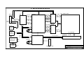
I. BLOCK DIAGRAM
VSYNC
HSYNC
VGA-IN
12PIN
C
O
N
N
E
N
DDC-SDA
T
DDC-SCL
ADC
SCALER
8 R0~R7
LVDS
10 EVEN
8 RA0~RA7
LCD PANEL(LVDS)
8 GA0~GA7
3 {R.G.B}
8 G0~G7
8 BA0~BA7
8 B0~B7
D-DE
8 RB0~RB7
D.D.C
24C21
LVDS
8 GB0~GB7
EEPROM
CRYSTAL
10 ODD
8 BB0~BB7
24C16
HI VOLTAGE
12M HZ
EEPROM
MCU
SDA
SCL
POWER
SWITCH POWER
SUPPLY AND
REGULATOR
8PIN
3V
5V
CRYSTAL
12V
POWER
ADAPTER
INVERTER
BLK-ON/OFF
BRIGHTNESS
12M HZ
12V
12V
C
O
N
N
E
N
T
Title
FUNCTION KEY
Size
B
Date:
BLOCK DIAGRAM
Document Number
Rev
ORION
Tuesday, October 23, 2001
B
Sheet 1
of
1
VCC
C117
NC
D13
BAT54C
R79
4.7K
R66
47K
R77
47K
R67
8
VGA_VSYNC
R68
51
6
R71
51
5
NC
SCK
1
2
3
NC
SI
4
VSS
D9
DAN217K(NP)
1
R83
2.2K
D12
0.1uF(NP)
C128
0.1uF(NP)
C56
22pF
2
9
8
7
6
5
4
5
4
9
8
7
6
9
9
5
4
1
2
3
5
4
1
2
3
TP
5
4
TP
1
2
3
5
4
9
TP
GND
3
U10A
74LVC14-SOP14
4
1
J2
TP
PA-VSYNC
U10B
74LVC14-SOP14
GND_EARTH
GND
J1
R44
100
2
GND
J9
TP
TP
C62
22pF
NP
J. SCHEMATIC DIAGRAM
2
C129
R42
100
9
5
4
TP
DAN217K(NP)
1
VE
5
4
C93
0.01uF
2
C109
0.1uF(NP)
VGA_VSYNC
9
1
2
3
9
H4
8
7
6
2
H3
8
7
6
RED-ADC
H2
H1
8
7
6
2
VE
1
D8
SOGI
NC
1
75
C113
0.01uF(NP)
C108
0.1uF(NP)
R65
0R
2
C122
5PF
1
1
1
R76
DAN217K(NP)
1
1
2
C90
0.01uF
2
1
1
L24
BULL WILL FCM1608K-800T07
2
VE
1
D7
R
0.1uF
GREEN-ADC
C121
5PF
2,3,4,5
C66
R64
0R
2
75
L27
BULL WILL FCM1608K-300T07
V33
C106
0.1uF(NP)
L23
BULL WILL FCM1608K-800T07
R75
TP
DAN217K(NP)
8
7
6
D6
1
2
TP
V33
1
1
TP
C86
0.01uF
2
8
7
6
G
TP
J8
2
VE
1
8
7
6
75
L26
BULL WILL FCM1608K-300T07
BLUE-ADC
C120
5PF
J7
R63
0R
2
1
2
3
R74
J6
TP
1
1
L22
BULL WILL FCM1608K-800T07
1
2
1
2
3
DB15 JP2
--------------------4
1 GND
5
2 TEST
9
3 5V
13
4 HS
14
5 VS
15
6 SCL
12
7 SDA
6
8 RGND
1
9 R
7
10 GGND
2
11 G
8
12 BGND
3
13 B
1
J5
TP
1
1
B
3
L25
BULL WILL FCM1608K-300T07
3
DB15
13
1
VGA_HSYNC
D11
R82
100
C127
22pF
12
11
U10F
74LVC14-SOP14
10
R45
100
U10E
74LVC14-SOP14
PA-HSYNC
C70
22pF
Acer Incorporated
2
Title
NP
VGA INPUT
Size
Document Number
Date:
Friday, November 01, 2002
2
R81
2.2K
J4
1
J3
1
VE
DDC-SDA
VGA_HSYNC
VGA_VSYNC
DDC-SCL
1
3
3
NC
VCLK
1
D10
DAN217K(NP)
VCC
U13
24LC21
2
R58
OR(NP)
PIN7
7
VE
VE
cable
R70
2
10k
VCC
47
1
2
3
VCC
R
G
B
3
1
17 2
3
16 4
5
6
7
8
9
10
11
12
13
14
15
R72
1K
1
DDC-SDA
CN9
0.1uF
PIN7
1
2
3
4
1
DDC-SDA
DDC-SCL
1
4
1
DDC-SCL
200-100-AS576
A
Sheet 1
of
6
Rev
PWM0
R37
PWM1
LCD_VEE
audio pwm
(NP)
LCD_VEE_A
lvds_on
LCD_VDD
R30
1K
LCD_VDD_A
panel power on
LCD_VBL
R31
1K
LCD_VBL_A
inverter blk
PWM0_A
5
PWM1_A
6
LCD_VEE_A
3
LCD_VDD_A
3
LCD_VBL_A
5
SCL
SDA
RGB-B11
RGB-B10
RGB-B9
RGB-B8
RGB-B15
RGB-B14
RGB-B13
RGB-B12
RGB-B19
RGB-B18
RGB-B17
RGB-B16
RGB-B23
RGB-B22
RGB-B21
RGB-B20
SDA
R36
SCL
SDA
R35
SCL
4
10K
4
10K
RESET
10K
R34
RGB-B[0..23]
4
4
inverter pwm
PWM1_A
1K
R38
VCC3-DCV
4
4
PWM0_A
1K
R29
3
VDDCRTL_T
LCD_VDD_A
3
5
INV_EN_T
LCD_VBL_A
5
IRQ-
3
PA-VSYNC
1
PA-HSYNC
1
C51
C53
100uF/16V
0.1uF
0.1uF 0.1uF 0.1uF
C57
C61
1
2
3
4
5
6
7
8
9
10
11
12
13
14
15
16
17
18
19
20
21
22
23
24
25
26
27
28
29
30
31
32
33
34
35
36
37
38
39
40
SOGI
DIBVDD
CAP_HREF
CAP_HSYNC
CAP_VSYNC
DIBVSS
BLU_INB_0/Y0
BLU_INB_1/Y1
BLU_INB_2/Y2
BLU_INB_3/Y3
BLU_INB_4/Y4
BLU_INB_5/Y5
BLU_INB_6/Y6
BLU_INB_7/Y7
DCVDD
GRN_INB_0
GRN_INB_1
GRN_INB_2
GRN_INB_3
GRN_INB_4
GRN_INB_5
GRN_INB_6
GRN_INB_7
DCVSS
RED_INB_0/UV0
RED_INB_1/UV1
RED_INB_2/UV2
RED_INB_3/UV3
RED_INB_4/UV4
RED_INB_5/UV5
RED_INB_6/UV6
RED_INB_7/UV7
DIBVDD
DVDD
DVSS
DTEST
DVCC
DGND
VGA_VSYNC
VGA_HSYNC
SOGI
U8
MASCOT V
AVCC
AGND
VREF
CP
CZ
VCCAB
BI
GNDAB
BCLP
VTOP
VBOT
VCCAG
GI
GNDAG
GCLP
TOUTP
TOUTM
VCCAR
RI
GNDAR
RCLP
PLLVDD
PLLVSS
DCVSS
OSD_FSW
OSD_CLK
OSD_R
OSD_G
OSD_B
OSD_I
DCVDD
RESERVED
XTAL
XTALI
DIBVSS
DISP_DE
DISP_VSYNC
SHCLK
DISP_HSYNC
DCVSS
1
C39
160
TVCLK 159
IRQ 158
SCS
157
SDA 156
SCL 155
RST 154
GPIO1 153
GBIO0 152
DCVSS 151
CONFIG4 150
CONFIG3 149
CONFIG2 148
CONFIG1 147
CONFIG0
146
PWM0
145
PWM1
144
DCVDD
143
LCD_VEE
142
LCD_VDD
141
LCD_VBL
140
DCVSS
139
RED_OUTB_7
138
RED_OUTB_6
137
RED_OUTB_5
136
RED_OUTB_4
135
DOBVDD
134
RED_OUTB_3
133
RED_OUTB_2
132
RED_OUTB_1
131
RED_OUTB_0
130
DOBVSS
129
GRN_OUTB_7
128
GRN_OUTB_6
127
GRN_OUTB_5
126
GRN_OUTB_4
125
DOBVDD
124
GRN_OUTB_3
123
GRN_OUTB_2
122
GRN_OUTB_1
121
GRN_OUTB_0
VCC3-DCV
VADCA
120
119
118
117
116
115
114
113
112
111
110
109
108
107
106
105
104
103
102
101
100
99
98
97
96
95
94
93
92
91
90
89
88
87
86
85
84
83
82
81
RGB-B7
RGB-B6
RGB-B5
RGB-B4
RGB-B3
RGB-B2
RGB-B1
RGB-B0
1
BLUE-ADC
1
GREEN-ADC
C65
C85
C89
C92
100uF/16V
0.1uF
0.1uF
0.1uF
0.1uF
VADCA
RGB-A19
RGB-A18
RGB-A17
RGB-A16
RGB-A15
RGB-A14
RGB-A13
RGB-A12
RGB-A11
RGB-A10
RGB-A9
RGB-A8
RGB-A7
RGB-A6
RGB-A5
RGB-A4
RGB-A3
RGB-A2
RGB-A1
RGB-A0
VCC3-DCV
C95
C96
C63
C58
C54
C52
C46
C45
C44
0.1uF
0.1uF
0.1uF
0.1uF
0.1uF
0.1uF
0.1uF
0.1uF
0.1uF
VADCP
RED-ADC
CP
CZ
VADCP
C107
R53
C87
0.01uF
C83
3
SHCLK
3
DISP-VSYNC
3
DE
3
C91
VADCP
C82
DISP-HSYNC
0.01uF C88
1M
4700p
C94
C101
0.01uF
0.1uF 100uF/16V
4700p
C77
150pF
X2
4700p
C97
22pF
CP
C84
12MHZ
C98
22pF
CZ
L20
BE0805
0.039uF
L21
BE0805
VADCP
VREF
R52
2.2K
VADCP
3
V=2.5V
L10
BE0805
TU3
1
TL431
C111
0.1uF
C112
0.01uF
C124
100uF/16V
Acer Incorporated
2
1
C75
RGB-A[0..23] 3
RGB-A23
RGB-A22
RGB-A21
RGB-A20
41
42
43
44
45
46
47
48
49
50
51
52
53
54
55
56
57
58
59
60
61
62
63
64
65
66
67
68
69
70
71
72
73
74
75
76
77
78
79
80
VADCA
VCC3-DCV
DOBVSS
BLU_OUTB_7
BLU_OUTB_6
BLU_OUTB_5
BLU_OUTB_4
DOBVDD
BLU_OUTB_3
BLU_OUTB_2
BLU_OUTB_1
BLU_OUTB_0
DOBVSS
RED_OUTA_7
RED_OUTA_6
RED_OUTA_5
RED_OUTA_4
DCVDD
RED_OUTA_3
RED_OUTA_2
RED_OUTA_1
RED_OUTA_0
DCVSS
GRN_OUTA_7
GRN_OUTA_6
GRN_OUTA_5
GRN_OUTA_4
DOBVDD
GRN_OUTA_3
GRN_OUTA_2
GRN_OUTA_1
GRN_OUTA_0
DOBVSS
BLU_OUTA_7
BLU_OUTA_6
BLU_OUTA_5
BLU_OUTA_4
DOBVDD
BLU_OUTA_3
BLU_OUTA_2
BLU_OUTA_1
BLU_OUTA_0
Title
MASCOT V(A/D+Scaler)
Size
Document Number
Date:
Friday, November 01, 2002
Rev
A
200-100-AS576
Sheet
2
of
6
RP5
RP6
RGB-B15
RGB-B14
RGB-B13
RGB-B12
RGB-B11
RGB-B10
RGB-B9
RGB-B8
1
2
3
4
1
2
3
4
RGB-B7
RGB-B6
RGB-B5
RGB-B4
RGB-B3
RGB-B2
RGB-B1
RGB-B0
1
2
3
4
1
2
3
4
RP7
33X4
RO0
RO1
RO2
RO3
RO4
RO5
RO6
RO7
8
7
6
5
8
7
6
5
PANEL
U3
GO0
GO1
GO2
GO3
GO4
GO5
GO6
GO7
8
7
6
5
8
7
6
5
RP8
33X4
RP9
33X4
8
7
6
5
8
7
6
5
BO0
BO1
BO2
BO3
BO4
BO5
BO6
BO7
RO2
RO3
RO4
RO5
RO6
RO7
44
45
47
48
1
3
GO2
GO3
GO4
GO5
GO6
GO7
4
6
7
9
10
12
BO2
BO3
BO4
BO5
BO6
BO7
13
15
16
18
19
20
D-HSYNC
D-VSYNC
D-DE2
D-SHCLK2
RP10 33X4
1
2
3
4
1
2
3
4
RGB-A23
RGB-A22
RGB-A21
RGB-A20
RGB-A19
RGB-A18
RGB-A17
RGB-A16
RP11 33X4
8
7
6
5
8
7
6
5
CVDD
R16
4.7K
Y1M
Y1P
D12
D13
D14 BLUE
D15
D16
D17
22
23
25
26
VCC
VCC
VCC
SHTDN
29
39
38
RIN1RIN1+
35
34
RIN2RIN2+
33
32
CLKCLK+
40
GND
GND
BO7
LCDVDD
LCDVDD
LCDVDD
RO7
DE
GND
RO0
RO1
RO2
RO3
1
RO4
RO5
RO6
RO7
30
BE0
BE7
0.01uF
0.1uF
GND
GND
GND
GND
GND
LVDSGND
PLLGNDLVDSGND
PLLGNDLVDSGND
5
11
17
24
46
GND
0.1uF
L2
BE0603
GND
LVDSVCC
37
42
36
31
GO0
GO1
GO2
GO3
GO4
GO5
GO6
GO7
RE7
C30
C31
1
BO0
BO1
BO2
BO3
CVDD
1
2
3
4
1
2
3
4
RGB-A15
RGB-A14
RGB-A13
RGB-A12
RGB-A11
RGB-A10
RGB-A9
RGB-A8
THC63LVDM63A
GE0
GE1
GE2
GE3
GE4
GE5
GE6
GE7
L4
1
RGB-A7
RGB-A6
RGB-A5
RGB-A4
RGB-A3
RGB-A2
RGB-A1
RGB-A0
1
2
3
4
1
2
3
4
2
BE0
BE1
BE2
BE3
BE4
BE5
BE6
BE7
+
C10
C19
2
DE
SHCLK 1
L11
33R
+
22u/6.3V(NP)
0.1uF
2
1
L12
0R
C1
C3
0.1uF
0.1uF
C2
C7
C5
C22
22u/6.3V
0.1uF
0.1uF
0.1uF
RIN2RIN2+
CLKCLK+
GND
GND
GND
RE4
RE5
RE6
RE7
C80
22pF(NP)
33PF(NP)
33PF(NP)
GND
DISP-HSYNC
R47
33R
2
DISP-VSYNC
R51
33R
C35
GND
C27
100uF/16V
(NP)
L6
BE1206
0.1uF
(NP)
D-HSYNC
D-VSYNC
C25
0.1uF
VCC
C71
100pF(NP)
GND
LCD_VDD_A
3
1
GND
R15
C20
10K
0.1uF
C26
0.1uF
2
Q3
2N3904
L1
BE1206
PVCC
R19
4.7k
GND
2
8
7
6
5
3
2
1
GND
R91
10K(NP)
C103
100pF(NP)
U4
Si9435
4
2
GND
V33
D-HSYNC
D-VSYNC
D-DE2
D-SHCLK2
GND
GND
M/B
1
GND
GND
LCDVDD
GND
GND
PANEL
CN6
BE7
BE6
BE5
BE4
30
29
28
27
26
25
24
23
22
21
20
19
18
17
16
15
14
13
12
11
10
9
8
7
6
5
4
3
2
1
1
2
3
4
5
6
7
8
9
10
11
12
13
14
15
16
17
18
19
20
21
22
23
24
25
26
27
28
29
30
BE3
BE2
BE1
BE0
GE7
GE6
GE5
GE4
GE3
GE2
GE1
GE0
RE7
RE6
RE5
RE4
RE3
RE2
RE1
RE0
1
30
30
1
M/B
FH-12-30S-0.5SH
CNA6
TM150XG-26L06A
GND
C6
100uF/16V
1
IN
GND
C102
RO3
RO2
RO1
RO0
GND
GE4
GE5
GE6
GE7
BE4
BE5
BE6
BE7
VCC
2
C73
RO7
RO6
RO5
RO4
XF2H-3015-1
GE0
GE1
GE2
GE3
BE0
BE1
BE2
BE3
L5
BE1206(NP)
33R
GO3
GO2
GO1
GO0
GND
GND
D-DE2
R50
GND
RE0
RE1
RE2
RE3
PS : SHCLK & D-SHCLK ADD GND
DE
GND
GO7
GO6
GO5
GO4
45
FH-12-45S-0.5SH
20
19
18
17
16
15
14
13
12
11
10
9
8
7
6
5
4
3
2
1
CN1
RIN0RIN0+
D-SHCLK2
2
GND
BO3
BO2
BO1
BO0
45
GND
RIN1RIN1+
GND
SHCLK
V33
V33
CVDD
RP15 33X4
8
7
6
5
8
7
6
5
GND
BO7
BO6
BO5
BO4
40
39
38
37
36
35
34
33
32
31
30
29
28
27
26
25
24
23
22
21
20
19
18
17
16
15
14
13
12
11
10
9
8
7
6
5
4
3
2
1
HEADER 20
LCDVDD
LCDVDD
RP16 33X4
PS : SHCLK & D-SHCLK ADD GND
2
GND
BE0805
RP14 33X4
GND
GND
V33
CVDD
GND
GND
GND
D-SHCLK2
GND
D-DE2
GND
RP12 33X4
RP13 33X4
8
7
6
5
8
7
6
5
GND
GND
BO4
BO5
BO6
BO7
C11
0.1uF
LCDVDD
CNA3
GO7
CVDD
2
8
21
C32
PLLVCC LVDSVCC
30
28
C12
0.01uF
RIN0RIN0+
GE7
D18 H_SYNC
D19 V_SYNC
D20 ENABLE
DCLK
BE0603
L3
C13
0.1uF
RED
Y2M
Y2P
D6
D7
D8 GREEN
D9
TCLKM
D10
TCLKP
D11
27
RE0
RE1
RE2
RE3
RE4
RE5
RE6
RE7
Y0M
Y0P
41
40
1
1
2
3
4
5
6
7
8
9
10
11
12
13
14
15
16
17
18
19
20
21
22
23
24
25
26
27
28
29
30
31
32
33
34
35
36
37
38
39
40
41
42
43
44
45
XF2H-4015-1
M/B
D0
D1
D2
D3
D4
D5
2 LCD_VEE_A
2 RGB-A[0..23]
CN3
TM150XG-26L06A
33X4
33X4
PANEL
1
20
1
1
2
3
4
1
2
3
4
20
RGB-B23
RGB-B22
RGB-B21
RGB-B20
RGB-B19
RGB-B18
RGB-B17
RGB-B16
2 RGB-B[0..23]
OUT
3
Acer Incorporated
TU1
EMI KHLC-010(NP)
Title
OUTPUT CONNECTOR
Size
Document Number
Date:
Friday, November 01, 2002
GND
Rev
A
200-100-AS576
Sheet
3
of
6
NC
VCC
MCU_CLKPP
R
GND
VCC
3
VCC
MCP-810(NP)
RESET
2
NC
VCC
C15
C17
C34
+
VCC
0.1uF
R8
10K
V6300-TO92
RESET
R17
X1
2
11.0592MHZ
R26
D1
C18
35
1M
22pF
21
CLK
1N4148(NP) 1K(NP)
JWT-A2001WV2-06(NP)
20
P1
10
6
5
4
3
2
1
44
43
42
41
40
RESET
39
38
MCU-W78E62B-PLCC 37
36
35
34
33
32
31
30
29
RESET
2
2
IRQ-
IRQ-
14
15
16
17
ROT_PB0
2
3
4
5
6
7
8
9
POWER
SW_LEFT
SW_SCRL_RIGHT
MENU
AUTO
18
19
20
21
22
23
24
25
26
27
28
7
8
9
10
11
12
13
14
15
16
17
BRI-ADJ
PWM0_A
2,5
U2
EA/VP
X2
SOCKET PLCC44
RESET
P1.0
P1.1
P1.2
P1.3
P1.4
P1.5
P1.6
P1.7
RD
WR
PSEN
ALE/P
TXD
RXD
43
42
41
40
39
38
37
36
ORANGE
GREEN
AUD_OFF
24
25
26
27
28
29
30
31
ROT_PB6
ROT_LF
19
18
32
33
13
11
TxD
RxD
8
VSS
A0
A1
A2
WP
6
R10
510
NC
DDC-SCL
1
DDC-SDA
1
VCC
NP
SCL
SDA
R5
6
33R
5
R3
SCL
2
SDA
2
R1
75R
33R
R13
0R
2
4
1
2
3
7
VCC
C4
0.1uF
P2.0
P2.1
P2.2
P2.3
P2.4
P2.5
P2.6
P2.7
INT0
INT1
T0
T1
R93
U1
P0.0
P0.1
P0.2
P0.3
P0.4
P0.5
P0.6
P0.7
X1
1
2,5
R9
10K
1
12
22
34
23
VCC3-DCV
R2
10K
44
VCC
VCC
1
INT2
INT3
VSS
P4.0
P4.1
1 V
2 R
3 G
GND
TU2
6
5
4
3
2
1
3
6
5
4
3
2
1
22pF
10uF/16V(NP)
CN4
SCL
SDA
TxD
RxD
VCC
R92
NP
1
G
2
U6
MCP-810
V
LED_G
24C16B
ROT_LF
ROT_PB6
ROT_PB0
1
4
3
2
1
3
Q1
2 2N3904
RP3
NP
4.7KX4
R12
150R
RP4
8
7
6
5
33X4
LED_O
VCC
1
2
3
4
8
7
6
5
R14
0R
2
RP2
MENU
SW_SCRL_RIGHT
SW_LEFT
POWER
ORANGE
33X4
LED_G
LED_O
PROVIEW KEY PAD --OK
R7
1K
R20
4.7K
3904
C
1
3
Q2
2 2N3904
B
E
2
1
2
3
4
1
VCC
1
RP1
4.7K
GREEN
5
6
7
8
1
2
3
4
5
6
7
8
4.7K
R6
1K
VCC3-DCV
4
3
2
1
1.Power
2.LED O
3.LED G
4.DOWN5.UP
6.MENU
7.AUTO
8.GND
R11
VCC3-DCV
VCC
5
6
7
8
CN2
WAFE-8PIN-1.5MM-90@
R4
AUTO
R18
1
2
C14
VCC
C16
C23
0.1uF 0.1uF 0.1uF
C21
C8
C9
C24
0.1uF 0.1uF 0.1uF 0.1uF
Acer Incorporated
4.7K(NP)
Title
MCU & LCD POWER CONTRIL
Size
Document Number
Date:
Friday, November 01, 2002
Rev
A
200-100-AS576
Sheet
4
of
6
CN12
2
S3
F1
FUS1206-5A
VIN12V
5
Choose one package
NP
VIN
L19
4
C118
0.1uF
C110
0.01uF
JBT0385-100805-4
3
1
DC-JACK
S4
NP
GND
GND
L18
BE1206
VIN1
C67
220uF/16V
R54
JUMP WIRE15MM
S2
300p
C79
330uF/16V
D2
MMSZ5248B(NP)
SB340
R55
R46
2K_1% 6.2k_1%
GND
C55
0.1uF
C59
220uF/16V
GND
GND
1
3A
VIN
220uF/16V
0.1uF
+
VCC3-DCV
VCC3-DCV 1,2,3,4
GND
On/Off
Bri
C119
220uF/16V
0.1uF
1
VADCA
AGND
VIN
VCC
C64
BE0805
100uF/16V
C60
0.01uF
R23
VADCA
2
OPVCC
NP
OPVCC
2N3094
GND
GND
R33
1K
R40
2.2K
U5A
LM358-SO8
GND
VADCA
2
GND
C74
L9
LCD_VBL_A
4.7K
C36
C33
0.1uF
2
0.1uF 0.01uF
1
1
Q52
4
VADCP
R39
3
Q4
2
2N3904
3
INVERTER I/F
VADCP
3
ADJ
1
C116
0.1uF
4.7K
GND
VADCP
C69
C48
CN5
1
2
3
4
5
6
U12
AIC1720-3.3
R28
220uF/16V
0.01uF
JST-2.0-6PIN
OUT
VCC
R32
C28
0.1uF
C47
GND
IN
1
4.7K
C43
<Part Type>
2
0
0
1,2,3,4
VCC3-DCV
C38
4
1
1
VCC
V33
2
0
R21
0R
R27
NP
NC
GND
3
PWM0_A
2
+
C42
100uF/16V
C29
0.1uF
AGND
OPVCC
GND
R41
2.2K
2
8
C
OUT1
0.1uF
NG 0514
+
OUT
0.01uF 220uF/16V
VIN
U7
AIC1084-33CM
IN
C50
0.1uF
GND
V33
C41
+ C40
C49
GND
V33
VCC
VCC
GND
R49
20K(NP)
3
L8
BE1206
0R
1
1
0R
S1
2
2
D3
D4
1N5822(DIP)
GND
R43
0.02-1/4W
L7
47UH@3A
CEM9435A SO8
AIC1578-SO8
C68
8
7
6
5
GND
GND
GND
8
7
6
5
D4
D3
D2
D1
2
R48
10K
CS+
CSDRI
GND
U9
S1
S2
S3
G
2
C72
0.01uF
VIN
DUTY
SHDN
FB
1
2
3
4
1
1
2
3
4
1
C78
0.1uF
D5
MMSZ5248B(NP)
U11
-
GND
GND
GND
Acer Incorporated
Title
POWER SUPPLY
Size
Document Number
Date:
Friday, November 01, 2002
Rev
A
200-100-AS576
Sheet
5
of
6
1
CN8
C104
MODE VCC OP VOL
10uF/16V
C131
L16
VCC_AU
2
1
MODE GND OP MAX
33PF
BE0805
R78
DEL L15
DEL L17
R69
NP
R73
1K
2
VCC
VCC
C125
0.1uF
C115
0.1uF
R85
33K
20K
DEL C134
DEL R86
13
12
11
10
9
AUD4835_SD
AUD_OFF
R61
10K
3
R60
10K(NP)
18
Right Dock
Shutdown
DEL R89
CN7
17
Left out-
15
Left out+
HI HP OUT
LOW SP OUT
21
Right out+
28
Right out +
L14
BE0603
BASE2S
R-SPOUT
1
2
Right Out-
Right out-
26
R-OUT
CN8
DC_Vol
R59
C123
2
2.2UF/16V
C99
0.0068UF
R56
20K
APA4835&4838
R57
33K
20K
L
C100
U5B
R
4
GND
7
L-OUT
Gain Select
C126
0.1uF
R22
2.2K
Lift Gain2
19
Lift Gain1
27
Right In
1
R62
10K(NP)
Left out -
Right out -
7
R24
1K
VDD
16
HP Sense
Right Out+
2
AUD4835_DCVOL
C130 1UF
Lift out +
Beep In
22
4
Lift In
R80
20K
HI SHUTDOWN
VCC
1
2
Right Gain2
C133 1UF
C135
0.0068UF
BASE2S
L-SPOUT
Left Dock
Right Gain1
20K
C132 1UF
24
RIGHTIN
R90
20K
GND
GND
GND
GND
GND
GND
CN11
SCP606
R88
Lift out -
1
8
14
20
23
29
LEFTIN
Left out +
L13
BE0603
Mute
Bypass
CN10
SCP606
20K
25
R84
20K
Mode
VDD
4
5
VDD
U14
6
R87
LM358-SO8
6
5
33PF
R25
2.2K
MRT
GND
PWM1_A
2
+
8
CN8 CN7
+
OPVCC
GND
C37
47uF/16V
+ - + -
R L
MUTE
0
MODE
GAIN
1
1
SDWN
0
HPS
0
Acer Incorporated
Title
AUDIO 4835
Size
Document Number
Date:
Friday, November 01, 2002
Rev
A
200-100-AS576
Sheet
6
of
6