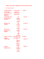
1
V.small V.light V.desirable ...
and now V.colours
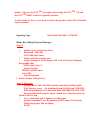
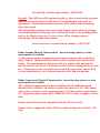
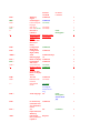
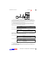
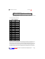
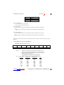
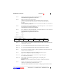
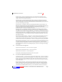
Introducing the Motorola V.3688
in two new colours
Express Yourself
¥
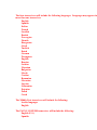
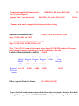
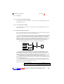
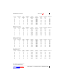
Now exists in three distinctive and
unique colours:
- Black
- Radar Blue
- Titanium
¥
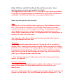
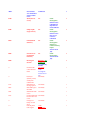
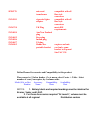
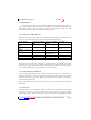
1999 Motorola Quantitative
Research showed the new colours
to be:
- Classy
- Smart
- Bright
- Eye-catching
- Modern
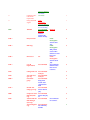
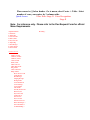
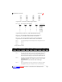
The Story So Far
¥
¥
¥
¥
¥
V. series launched in March 1999
in EMEA as the smallest and
lightest GSM Dual-band phone in
the world
Black colour well received by
consumers
Launched with heavyweight panEMEA advertising
Supported by dedicated PR and
promotional material
Distributed in all mainstream
outlets
The Brand Promise
¥ Show your world that
youÕve made it
The Brand Character
Ð Stylish
Ð Outgoing
Ð Trend-setting
Target Consumer
¥
¥
¥
¥
¥
¥
Those who seek products that will help
them feel important within their group
Those who like to have fun by keeping in
touch with their friends
These consumers choose products with
badge value to convey an image of
success
Men and women between the ages of 18-34
Those who are more willing to pay for
products they value
They like to be noticed using a distinctive
communications device
Key Benefits
¥
¥
Functional
Ð One of the smallest and lightest
phones in the world
Ð Ease of use, portability
Ð External badge
Emotional
Ð ÒLook at MeÓ: Tells everyone
that I have style
Ð Colour for colourful me
Ð IÕm modern, elegant, youthful
and fun
Ð Self fulfilment and self expression
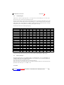
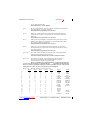
Product Features
¥
¥
¥
¥
¥
¥
¥
Amazingly small and colourful
SMS (Short Message Service)
capable
VibraCallª alert
Optimaxª full graphics
Hands-free headset accessory
New mini Rae charger
Increased talktime and standby
time due to new 600 mAh LiIon
battery as standard
Quick Reference Guide
Basic Operation
Quick Access Interface
Store to Phone book
Quick Reference Guide
Memory Dialling
Quick Reference Guide
Special Features
Control
¥ Customisable Quick Access Menu
- Place nine of your most frequently
used features in your own personal
menu so that they can be accessed
with just two key presses. Icons make
each feature easy to identify.
Power
¥ Superb battery performance
Each phone is capable of several hours
conversation or several days standby,
but is still small and light. Use both 900
and 1800 MHz bands for greater call
success and allow wider roaming
opportunities.
Quick Reference Guide
Special Features
Discretion
¥ VibraCallª
- In locations where
you donÕt want your phone to ring, or
which are too noisy to hear your phone
ring, your phone can vibrate to alert
you of a call.
¥
¥
Wearable Holster - Wear your phone in
a stylish holster on your belt. It is small
enough and light enough to keep with
you almost anyway.
Stop Call Alert - Press either volume
buttons when the phone is ringing or
vibrating. This will stop the alert but
not answer the phone.
Quick Reference Guide
Special Features
Personalityª
¥ Unique to Motorola. Personality ª
allows you to personalise the way you
use your phone - for example, different
ringer tones, a phone book and
network selection preferences - all
presented with clarity and simplicity,
identifiable with an
symbol.
Accessories
Chargers
In-car
Accessories
Car Kits
Hands-free
Accessories
Smart Handset
Data Solutions
Carry Solutions
In-car Phone
Charger
CLA9000
Portable
Hands-free Kit
HSK9000
Smart Leather Case
Black CCA9060
Tan CCA9061
Leather Pouch
Black CCA9050
Tan CCA9051
Plastic Holster
CCA9150
Mini Travel Charger
with Euro Plug
CHA9050
With UK Plug
CHA9060
Mini Desktop
Charger Base
CHA9250
Professional DSP
VR Hands-free
Car Kit
HFK9450A
Smart Handset for
DSP Car Kit
HSK9380
Smart CELLectª
PCC9050
56k Global Modem
PC Card
PCC9560
New Packaging
¥
KAG TO DROP IN VISUALS UPON APPROVAL
After Sales Service
¥
¥
¥
General consumer helplines for pre
& post sales enquiries (same No. as
cellular & paging)
12 months warranty
Helpline for advice on service
policy
An Integrated Pan EMEA Advertising,
PR and POS Campaign
¥
¥
¥
¥
¥
30 second TV Commercial available to all
markets from September
New Print campaign featuring designs from
Mathew Williamson (leading fashion
designer) from October
Specific market media (e.g. Use of buses
during London Fashion week)
Market specific PR activity focusing on
driving awareness of new colours in a stylish
and fashionable way
Eye-catching POS and merchandising
materials based on the print creative
Summary - Launch Plan
¥
¥
¥
¥
¥
¥
Launch of 2 new colours
New logo and graphic that builds on
style and brand character of stylish,
outgoing and trend setting
New TV and Print campaign
supported by heavyweight PR, POS
and merchandising
Product in market 30 September
TV Commercial on air from September
Print Campaign from October
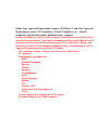
V.small V.light V.desirable V.colours
Product Description
Internal Name: Kramer / Market Name: v3688
Created By:
Pete Thompson-WPT003/LIB/Motorola CSS on 17.02.98 at 17:45
State:
Review
Version Number: 13
Hot Spot to PR Number Assignment database. This Hot Spot for use by ECSG personnel
only.
Click in Hot Spot, to view, or to generate a request for a Product Release (PR) number.
PR Number: A28-19
Motorola Confidential Proprietary
Insert Table in field below to define key changes. Go to Menu -> Create -> Table. Make
table 4 columns wide.
Enter brief summary of any updates below:
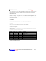
Change Control:
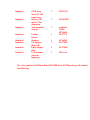
Version Number
4
Date
2/17/98
Editor
Jim Filicette
Key Changes
Move from Word
to Notes
Revise unique
features list
Add third battery
door/battery
requirement
Add white
holographic
display
requirement
Add to lens
description
Update software
requirements per
the plan
Add hardware
tracking list
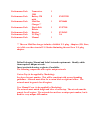
5
11/MAR/98
Tracey Koziol
6
7
26/Mar/98
Ruchi Mangalik
8
9 June '98
Updated
software
features
Incorporated
GSM 1900 Req
Updated
hardware
features
Included
competitive
table
Updated Key
selling points
Updated
software
features
Updated
hardware
features
Updated
Manual
requirements
Updated Stage
2 requests
Changed VA
reqts to 3min
Changed VR
reqts to 25/15
Updated
TT/SBY based
on eng.
Updated
electrical perf
Pete Thompson general update
of entire
document
added
additional
software
requirements
added detail
regarding colors
and styling ring
moved VA/VR to
Stage II
added available
part numbers
9
25 June '98
Pete Thompson
Added:
Asian model
numbers and
package
structure
market name
per new
naming
convention
GSM1900 PA
output
Stage 1 for
GSM1900
increased
housing wall
thickness
requirement
3 software
features
requirement
for 4M part
support
list of items
under
negotiation at
the current
time
(Appendix)
light and dark
metallic grey
battery doors
Voice
Activated
hands free car
kit
requirement
language
splits for
different
transceivers
Changed:
inside
escutcheon
label
signature
approval list
Deleted:
wireless
headset
requirement
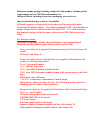
10
8 July '98
Pete Thompson
Updated "Key
Software
Requirements
" section
Updated "Key
Hardware
Requirements
" section
Moved styling
ring
implementatio
n to Stage II
Revised
Approval
Signature list
In
"Introduction"
section,
indicated
there will NOT
be a 900 / 1900
follow-on
product
Added
requirement
for Y-cable
Added
responsibility
to all planned
accessories
Added
requirement
for Marketing,
Dummy, and
CeBIT
samples
Added Asian
sample
request
numbers
Added Asian
transceiver
number
11
17 July '98
Pete Thompson
12
03 August '98 Pete Thompson
Added PACSG
Sample
Requirements
Added PACSG
Approval
names
Added that
lens and
keypad will be
common
across all
regions
Changed
requirement
for one-piece
packaging
across all
regions
Added bulk
packaging
requirement
for PACSG
Added 3
names to
approval list
Added 14x15
Asian bitmap
requirement in
all builds /
testing
Confirmed
stub antenna
use for Stage I
launch
Added
GSM1800/1900
receiver
sensitivity
Increased EP
Alert level to
98 db SPL
Software
Requirements:
-added dates
when answers to
open issues are
due
-added
clarification for
several items
-added
"Emergency
Dialing" section
under 3.3
Added 4 items
to be
considered for
future
products
(Section 7.)
Changed
language
bundling
requirement
for EMEA
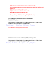
13
4 January '99 Pete Thompson
NOTE:
Updating is IN
PROCESS
changed
market name
from "V3688"
to "v3688"
added "Social
Networkers"
and "Business
Achievers" as
target
segments
revised
weights,
volumes, talk
and standby
times
Smart Card
requirement
deleted
added
Motorola
numbers for
proposed
housing
colors
Insert Table in field below to define release approvals. Go to Menu -> Create -> Table.
Make table 3 columns wide.
When ready for release, submit for signatures. Define who signed below.
Each subsequent version change requires release signatures.
Release Approval Summary:
Version Number
Signed by
Date
VP/General Manager
Ralph Pini
Roger Kung
Frank Wapole
Engineering
Paul Dal Santo
Jay Smith
Roger Jellicoe
Duane Rabe
Program Manager
Bruce Hirtzer
Marketing
Mark Powell
Tracey Koziol
Pete Thompson
Paul Pelski
Ruchi Mangalik
Brian Harbison
Michelle Mindala
Cathy Stemple
Electrical
Mike Cruz
Ross Ripley
Mark Koziol
Steve Geske
Mechanical
Dave Trahan
Software
Henry Lee
Peter Demus
Roman Sikaczowski
Mike Hader
Steve Akin
Doug Main
Materials
Hiram Burrows
Rich Ward
Joni Berrettini
Accessories
Gayle Landuyt
John Calderone
Ed Rauch
Quality
Jorge Santos
Jim Wagner
Tom Shaw
David Cox
Distribution /
Packaging
Florian Janesak
Finance
Jim Gentile
Gray Benoist
Keith Gorse
Manufacturing
Finn-Lund Andersen
Glenn Gilstrap
Mike Hickey
Doug Wick
Peter Yeo
Market Name:
v3688
Ship Authorization date:
Stage 1 GSM 900/1800 Dec 1998
Stage 1 GSM 1900 Feb 1999
Stage 2 GSM 900/1800 REFRESH Mar 1999
Stage 2 GSM 1900 REFRESH Mar 1999
Note: The PACSG group will determine when Stage II GSM1900 product will
actually launch into the market, depending on market conditions at the time. (use
format DDMMMYY)
Give a general introduction for this product requirement.
The internal name for the GSM 900 /1800 product is Kramer, or StarTAC 210. The
analog equivalent is Vader.
This document describes the Global GSM StarTACTM product, known as Kramer.
Various references are made to the existing GSM StarTACTM 85/130 (clam Rae), or
other existing platforms/models. Only features that are different for Kramer are
documented below.
The product represents the first of a new generation of high tier StarTACTM phones
launching on a global basis across tecnology platforms making a global leadership
statement in areas of form factor , size and weight . The new StarTACTM will
provide additional capabilities from software, MMI, and hardware perspectives,
allowing Motorola to demonstrate its leadership in the social network segment of the
market. The new StarTACTM will replace the existing StarTACTM 130 and
StarTACTM 8000G as the new signature product.
As of Revision 10, there are no plans to follow this product with a 900 / 1900 mHz
capable product.
Signaling Type:
Dual Band (900:1800) / GSM1900
Define Key Selling Points and Message:
Stage I:
*
*
Smaller, more stylish form factor
Dual Band: 900/1800
GSM 1900 single band
*
Longer talk time/standby time
*
Large bit-mapped 96x54 display with 1 line of icons and Optimax
halographic film
SIM Toolkit (class 2)
Internal headset
FR/EFR and HR codecs
Asian SMS
Asian Phonebook
[* denotes Unique Selling Point]
Stage II (Refresh):
*
Styling rings to add color/differentiation potential and flip rigidity
WAP-internet access ( for both Dual Band 900/1800 and GSM1900)
PIM-alarm/scheduler ( for both Dual Band 900/1800 and GSM 1900)
Keypad-rubberized, negative image, domed keys with glossy glob top
finish as on Flat Zap
*
Voice Annotation with 3 minutes recording time
*
Speaker-dependent Voice Recognition with 25 names/15 functions
White halographic film on display
EGSM
Define Product Tier (High, Mid, or Low):
According to the new branding guidelines, this product will be in the Social
Networker, and Business Achievers tier.
Define Distribution Channel:
Same as existing StarTACTM family (operators, distributors, retail)
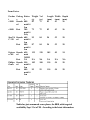
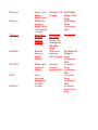
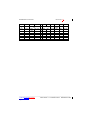
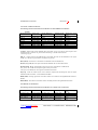
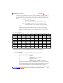
Define Competitors:
Performance
Product
Package
v3688
Standard
v3688
Best
StarTAC 130 Standard
StarTAC 130 Best
Ericsson 788 Standard
Ericsson 788 Best
Philips Genie Standard
Philips Genie Best
Battery
600 mah Li
Ion
1800 mah Li
Ion
600 mah Li
Ion
Main + Aux
Batt
650 mah Ni
MH
NA
550 mah Li
Ion
1000 mah
Ni MH
Talk time
(mins)
125 - 200
Standby time
(hrs)
40 - 110
450 - 680
150 - 380
100 - 140
35 - 50
390 - 540
140 - 190
144 - 180
38 - 60
NA
65 - 69
NA
42 - 80
300 - 450
100 - 150
Form Factor
Produc Packag Batter
t
e
y
v3688 Standa 600
rd
mah Li
Ion
v3688 Best
300
mah Li
Poly
StarTA Standa 600
C 130 rd
mah Li
Ion
Best
400
mah Li
Ion
Ericsso Standa 650
n 788
rd
mah
NiMH
Best
NA
Philips Standa 550
Genie rd
mah Li
Ion
Best
400
mah Li
Ion
Weight Vol
(g)
(cc)
83
72
Length Width Depth
(mm) (mm) (mm)
82
43
26
72
72
82
43
26
95
84
94
52
20
87
84
94
52
20
135
120
105
49
24
NA
102
NA
100
NA
110
NA
54
NA
20
95
99
110
54
20
Nokia has just announced a new phone, the 8810, with targeted
availability Sept / Oct of '98. According to the latest information:
Weight: 118 g (Standard battery), 98 g (LiIon battery)
Dimensions: 107 x 46 x 18 mm, 74 cc
Display: Illuminated high-contrast, full graphics with up to 5 lines for
text, numbers, graphics
Memory: 250 names and numbers in phone, up to 255 in SIM
Connectivity: built in infrared link
Data: built in GSM data capable
Performance:
Standard 600 mAh NiMH: Talk 1 h 40 min - 2 h 50 min; Standby 36
- 133 h
Vocoder: Full, Enhanced Full, and Half Rate
We believe the form factor to be similar to the 8110 but straight in
design. Ericsson intelligence also suggest a phone of weight 72g, no
other details available yet.
Define Key Target Customers:
Key target customers include those within the Social Networker and Business
Achiever market segment, plus individuals who desire a wearable light-weight,
feature rich product to compliment their business needs and personal lifestyle.
Define product tiering strategy, and any planned variants, for this product:
The new StarTACTM will be positioned above all the other StarTACTM products
and promoted as our flagship product.
Define Models to be Replaced by this Product:
Place cursor in field below. Go to Menu, select Create -> Table, then define
number of rows you require, by 3 columns.
Model Name
Model Number
Comments
StarTAC 130
SE0197AB1**
StarTAC 8500G
XXXXXXXXXXX
This model is
targeted for first
shipments end of
Aug '98. Market
conditions will be
evaluated at the
time of the Kramer
launch to
determine phase
out of StarTAC
130.
The replacement of
the 8500G is
expected, but is
dependent on
StarTAC chipset
evolution.
Define Target Markets:
Target segments are the Social Networkers and Business Achievers, as defined by the
new segmentation strategy.
Define Advertising Requirements, Specifications to Advertise, and Key Message to be
delivered:
As Motorola's flag ship product, the new StarTACTM will be advertised extensively
to reinforce the new corporate wireless products' brand campaign which is launching
in mid-98. All marketing communications, product literature, packaging, etc. must
help to convey the theme of the campaign by following guidelines for the use of
styling elements and brand messages.
The new StarTAC message will build on innovation and technological leadership of
the original StarTAC phone to support the primary message of our brand (creating a
broad range of innovative wireless tools for convenient communications through
mobility). Motorola has taken the next step in the evolution of the StarTAC family
by developing the next generation GSM StarTAC and creating the smallest and
lightest weight mobile phone in the world. Motorola has packed the new GSM
StarTAC full of features, such as high contrast display and VoiceNoteTM recording
capability (available in the Stage II launch). In addition to improvements in battery
performance allowing much longer talk and stand by times, the new StarTAC offers
an improved user interface with voice recognition (available in Stage II). The new
GSM StarTAC offers new color bands to accentuate the smooth stylish looks of this
world class product.
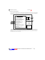
Define Phone Physical Characteristics. Insert drawings, photos, or other
representation if available.
The new StarTACTM will use a smaller form factor than any existing
StarTACTM GSM phones, but will retain the clam-style format.
Lightest Configuration
Weight: initial target 65 g
actual: 72 g
NOTE: Under a different directive (Jun '98), housing wall thicknesses has been
increased to add rigidity.
Volume: initial target 69 cc
actual: 72 cc
Packaged Configuration
Weight: initial target 77 g
actual: 83 g
NOTE: Under a different directive (Jun '98), housing wall thicknesses will be
increased to add rigidity.
Volume: initial target 69 cc
actual: 72 cc
Dimensions: length:82mm Width:43mm Depth:26mm
Define Housing Physical Characteristics. Insert drawings, photos, or other
representation if available.
The new StarTACTM will use all new housings. The housings are being
developed in parallel with the analog version of Kramer, which is known internally
is Vader. The phone will use a clam format in a new smaller form factor. The
battery will be in the lower half and the display will be in the upper half of the
phone. Finger cavities will be designed into the transceiver front on each side of
the keypad, but not on the flip front to allow easy single handed opening of the
phone. The housings will be made of poly-carb plastic, and will have a light
texture similar to cd920/930. The plastic must be suitable for production in black
and metallic colours (blue, dark grey, and light grey.) The plastic must be capable
of being painted.
The proposed housing colors are: Black, Radar Blue (Motorola number 628),
Galaxy Gray (Motorola number 615), and Light Titanium (Motorola number 630).
There will be a plastic styling ring on the outside edge of the top flip, available in
gloss black, metallic gold, and metallic chrome. Colors to be available for Stage II.
The styling ring will not be interchangeable by the end user.
Note: A changed directive (Jun '98) requires the wall thicknesses of the housing be
increased where possible to add rigidity. Achieving minimum weight by
minimizing wall thickness is no longer valid.
Other housing requirements include an opening for lanyard (upper left when
viewing the rear), LED opening (upper right center), alert port (top center),
earpiece connection (top right center), opening for rubberized button (top left
center) to activate Mute function (Stage I) or VoiceNote (Stage II), Aux Batt* slot
(top center rear) and mounting holes (bottom left and right), escutcheon pocket
below the keypad and front of top flip.
* The Aux Batt will NOT be supported for Kramer, however will be supported for
the analog Vader product.
Define Battery Door Physical Characteristics. Insert drawings, photos, or other
representation if available.
The battery will be situated on the rear of the phone's lower half, with an internal
battery pack with door configuration similar to Zap. Four battery doors will be
required: one for standard size battery packs, one for the extra capacity pack, one
for the high performance pack.
The doors must be rigid and feel very solid on the phone. There will be no bowing
or movement of the door plastic when force is applied to the back or sides of the
door. The door latching mechanism is different from Zap, in that the latch must be
slid upwards before the door can be removed. A metallic inlay with the Motorola
batwings must appear centered in the top half of the door. A gold colored inlay
will be used with a black and gold styling ring, while a silver inlay will be used with
chrome ring. A gold inlay will also be used when a styling ring is not part of the
product. An installation process must be used to eliminate the inlay from coming
out during the product life.
At ship acceptance, there must 500 of each of the non packaged doors in inventory
across all regional distribution centers.
NO Aux Batt will be available for the new GSM StarTACTM since battery power
management will make it unnecessary.
Define Display Physical Characteristics. Insert drawings, photos, or other
representation if available.
The new GSM StarTACTM will have one line of icons positioned at the top of the
display, a bit mapped 96x54 pixel graphic LCD display located on the top half of
the phone. The display will be capable of Asian SMS.
The display will be available in a standard back-lit format with green Optimax
holographic film for Stage I. White holographic film must be used for Stage II
launch.
14 x 15 bitmap for Asian characters must be included in all builds and testing
applications.
Define Lens Physical Characteristics. Insert drawings, photos, or other
representation if available.
Similar layout and design to the GSM StarTACTM 85 ( i.e Motorola logo will be
screened on the second surface at the top of the lens.) The lens must also be
covered with a hard coat to prevent scratching. The printing color must match the
styling ring being used, either gold or chrome. There may be a need for different
color borders to contrast with the housing. The lens will be common between
EMEA, Asia, and PACSG.
Define Keypad and Keypad Board Physical Characteristics. Insert drawings,
photos, or other representation if available.
The new StarTACTM will use a 19 key keypad. The keypad will have the same
functions as the currently shipping StarTAC 85, however the Call Voice Mail icon
will replace "MR". The keypad will be common across EMEA, Asia, and PACSG.
Due to engineering constraints, the new StarTACTM will ship with hard, flat keys,
similar to existing StarTACTM family. Market research demonstrates that
consumers dislike this type of keypad while they favor rubberized, negative image,
domed keys with a glossy glob top finish, as used on flat Zap. Engineering must
pursue a design as an alternative to the hard keypad after initial product launch.
Define Escutcheon Physical Characteristics. Insert drawings, photos, or other
representation if available.
External - top lip raised Oudensha with glob top ('Chrysler' sample) Motorola
logo. The background color must match the housing color. The printing color
must match the styling ring color and shine. For the black styling ring, gold
printing must be used. There will be a total of 4 unique escutcheons; black
background / gold printing, dark grey metallic background / silver printing, light
grey metallic background / silver printing, blue metallic background / either gold
or silver printing.
External flip escutcheon part number: 5403796S02
Internal - The GSM logo will be printed in gold (or silver for units with a chrome
band) on vinyl escutcheon, but will allow for co-branding in color print as
appropriate. The internal escutcheon pocket will be on the inside bottom flip,
below the keypad.
The background escutheon color must match housing colour, while the printing
color must match the styling ring color, either gold or silver. The printing will be
gold for the black styling ring. As above, there will be 4 unique internal
escutcheons with the same color scheme.
Internal transceiver escutcheon part number: 5403797S07
Define Antenna Physical Characteristics. Insert drawings, photos, or other
representation if available.
A stub antenna capable of supporting dual band operation will be available at
Stage I launch. This decision was based on stub vs. pullout style antenna field
testing. The antenna must be designed so the user cannot easily unscrew the
antenna with the bare hand. The antennas will not be interchangeable by the end
user. Both antennas (the retractable in both up & down positions and the fixed
version) should meet or exceed the performance of the Zap stub antenna.
Define Connectivity Physical Characteristics. Insert drawings, photos, or other
representation if available.
The v3688 must support internal data capability with 14.4 KBS data speed.
Internal data is defined as the ability to connect the phone to a PC with a dumb
cable with level shifters, with compression and AT Command Set resident on the
PC. Engineering must ensure that COMMUNICATE is ready to support 14.4 kbs
data.
Kramer must be backwards compatible with the CELLect Card 3.
Kramer will not support the Smart CELLect cable developed for StarTAC 130 /
Zap.
Define SIM Card, and SIM Card Reader Physical Characteristics. Insert
drawings, photos, or other representation if available.
Will support small SIM format, 3V/5V, 3V only and 5V only. Initial speed should
be 6x SIM, but the platform must not be limited to 6x as new faster standards are
established. The SIM card will fit into a tray underneath the battery.
Define any other physical characteristics.
Color:
Housing colors will be available in black, galaxy gray, light titanium, and radar
blue. These enhanced color plastics are critical in order to meet researched
consumer preferences a well as competitive offerings. Painting must be used for
achieving the desired colors. Sample housings must be painted and tested to
ensure Quality requirements are met. For shipping product, the housings must be
molded in the same color as the paint.
Stage I product will be black, while Stage II product will ship in black, galaxy
gray, light titanium, and radar blue.
Styling Ring:
A styling ring which outlines the perimeter of the top flip will be available in 3
metallic colors: Metallic black, chrome, and gold. All the rings will have a highly
polished, non-textured finish. The styling ring must provide rigidity also, and must
be plastic plated with either black, gold, or chrome finish. The black and gold
rings will be used with the black housing, the chrome ring will be used with the
galaxy gray, and light titanium, and radar blue.
Note: Market requirements indicate the need for the styling ring for Stage I
launch. See Appendix.
External keys and buttons:
Two volume keys, one smart button in the middle, and one Mute / VA button all
made of hard rubber. The Smart button must have a raised nib for easy
identification.
Since Voice Annotation will not be supported for the Stage I launch, the button will
be used as a Mute button. For Stage II launch, the button will support VA. The
button should be positioned on top of the bottom housing on the antenna side. The
button must be easy to locate and actuate.
External ports:
Hirose accessory connector -The new StarTACTM will have an accessory
connector on the bottom of the lower half, similar to current StarTACTM
products.
Headset port - The new StarTACTM will also have a port near the top of the
lower housing, oppposite of the antenna and near the status LED for direct
connection to a headset or HATIS or TTY device with a phone jack (i.e. without
adapter.) The port will support the existing Zap and StarTAC 130 headset.
Headset performance - using either headset option, performance must be the same
as or better than Zap and StarTAC 130 with regard to buzz and overall audio
quality / volume.
Alert Port - position should be optimised to ensure that when worn on the holster
the port is not concealed by clothing.
LED indicator:
Kramer will have an LED indicator located top right center with the same
functionality as StarTAC 130. Improvement to light intensity should be
investigated due to poor feedback from customers on existing products. The
flashing frequency and duration must be the same as currently shipping GSM
StarTAC.
Define Transceiver Performance:
Place cursor in [ ] below header. Go to menu, select Create -> Table. Select
number of rows you require, by 5 columns wide.
Volume (cubic cm)
Weight
(grams)
Talk Time
(minutes)
Standby
Time
(hours)
With
Battery
(Name)
69
initial
target 55*
actual 60
initial
target 65*
actual 72
-
-
Transceive
r only
60 - 95
20 - 50
72
initial
target 77*
actual 83
120 - 180
40 - 100
78
initial
225 - 340
target 98*
actual 105
190-320
78
actual 104 125 - 200
40 - 110
103
450 - 680
initial
target
143g*
actual 145
150 - 380
Transceive
r with a
12 g Li
Polymer
battery
Transceive
r with 600
mAh Li
Ion
battery
Transceive
r with 900
mAh Li
Ion
extended
capacity
battery
Transceive
r with 500
mah Ni
MH
battery
Transceive
r with
1800 mAh
Li Ion high
performan
ce battery
72
*NOTE: Under a different directive (Jun '98), housing wall thicknesses will be
increased to add rigidity.
NOTE : All battery performance times are approximate and will vary depending
on network configuration,band and status, functions selected, and type of SIM
card. If the SIM card does not support the Stop Clock feature, resulting standby
time will be significantly reduced. Times are quoted as a range from DRX2 to
DRX9. Support of DTX mode is dependent on network support and may not be
available in all areas. Performance quoted is for GSM only at this stage of the
Product Description. Engineering to provide GSM 1800 / 1900 performance numbers.
Note: There must be 500 each of the lightest (300 Li Polymer if available) and high
performance batteries (1800 mAh Li Ion) available at ship acceptance.
Technology:
GSM 900/1800 dual-band will have auto-band switching with flex capability for
Manual band select. GSM 1900 will only be supported in stage 1.
Vibrator:
The new StarTAC will incorporate an internal vibrator as good or better than the
StarTAC 130. Evaluation must be complete to determine if the 4mm vibrator is
strong enough.
Real Time Clock:
The new StarTAC will have a real time clock, which will be pixelized in the text
area of the display, near the bottom. The clock must NOT interfere with the name
of the Service Provider, or Asian characters. The clock should be compatable with
an alarm scheduler for Stage II launch. The real time clock will need to retain its
memory for a minimum of 2 weeks with the battery removed. The battery
dedicated for the real time clock will be rechargable.
Please refer to the Marketing Requirements Specification detailing positioning and
appearance of the Real Time Clock.
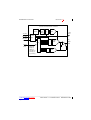
Electrical design:
The new StarTAC will utilise a 1.8V White Cap based chip set, Hirose (15 pin)
connector, 3.6V battery support, and the latest components to minimize both Tx
and Rx current drain. Lithium Polymer, Li Ion, and AAA NiMH battery
technologies will be supported. Below are performance targets for GSM 900:
Tx = 225mA
DRx2 = 5mA
DTx = 150mA
DRx9 = 2.5mA
Below are performance targets for GSM 1800:
Tx = 225mA
DTx = 150mA
Below are performance targets for GSM 1900:
Tx = 225mA
DTx = 150mA
DRx2 = 5mA
DRx9 = 2.5mA
DRx2 = 5mA
DRx9 = 2.5mA
Memory:
Given the number of software features and languages required, the transceiver
must be layed out for compatibility with a 4M part for Stage II. This remains an
open issue with Engineering. See Appendix.
Internal charging:
The new StarTAC will have EP internal rapid charging circuitry compatible with
Lithium Ion, Lithium Polymer, and NiMH.
Sensitivity and call completion rates:
The new StarTAC will have best in class sensitivity. Sensitivity and call
completion rates must be as good or better than Zap.
GSM 900 Receiver sensitivity: Target -107dBm static at the antenna
GSM 1800 Receiver sensitivity: -106 dBm static at the antenna
GSM 1900 Receiver sensitivity: -106 dBm static at the antenna
PA output GSM 900 only: 33dBm nominal
PA output DCS 1800 only: 30dBm nominal
PA output GSM 1900 only: 30dBm nominal
PA output with power cut software algorithms: 1.0 dB reduction from full output
power
EP Audio/Alert Improvements:
The new StarTAC will use a dynamic speaker. The ear piece audio will be
enhanced such that the audio distortion is minimized on networks with high audio
level while maintaining / increasing the volume level to meet customer satisfaction
when used on networks with low audio levels. At a minimum, the EP Alert levels
are 98 db SPL at 5cm nominal and engineering should try to improve these levels.
Define Battery Technology compatibility and Security requirements:
A new range of batteries will be developed using existing LiIon LSQ8 and LSQ6
cells and alumimium-can LiIon LSQ6 cells for lighter weight. Li-poly must be
supported for a super light weight battery. The high performance battery must be
1800 mAh Li Ion. Where possible, packs must be reusable with the AMPS Vader
product. ALL batteries must include the self protection circuit. The Invalid
Battery feature will be utilized for Kramer. This will make charging a battery
without an EEprom impossible, either in the phone or in the desktop charger.
Define Charge Times with the sharger shipped as standard:
Place cursor in [ ] below header. Go to menu, select Create -> Table. Select
number of rows you require, by 3 columns wide.
Battery
Charge time with E. Charge time with E.
P. Standard Travel P. Desktop Charger
to 90 % charge
Charger to 90 %
(Minutes)
charge (Minutes)
NiMH batteries
LiIon batteries up to 1000
mAh
Li Ion batteries over 1000
mah
70 minutes
2-1/2 hours
5 hours
The unit must feature seamless power transitions for desk/travel chargers and
CLA's, and warm plugging for other peripherals such as carkits, laptops and
PDA's.
Today's charge times for Li Ion 500/1000 mAh is currently acceptable but by 1Q
1999, improvement will be needed to a charge time of 1 to 1 1/2 hours.
Define Data Compatibility:
See "Connectivity" Section.
Define any requirements in general terms, or define overall requirements scope:
The software features are included from the software road map. All features from
StarTACTM 130/CD920/930 and Zap Refresh must carry forward into the new
StarTACTM .
Key Software Requirements:
Define Key Software Requirements. Insert drawings, photos, or other representation if
required, after table.
Place cursor in [ ] below header. Go to menu, select Create -> Table. Select number
of rows you require, by 5 columns wide.
Priority
Status Tracking Number Description
Status Main
First
Launch
Launch
0219 *
0068*
0196 *
0195**
0016
?*
?*
0218*
0216*
A0003**
0217**
0217**
0203**
*
0208*
0056*
?**
WhiteCap
support
EGSM support
Eastern European
languages
STK class 2
STK with unicode
STK with Ecommerce
STK class 2 with
Asian language
support
(Covered under
STK class 2
above)
Configuration
Mgmt (PCS)
Configuration
Mgmt (China)
Asian
SMS/Languages
96x54 row display
Pixelized Real
Time Clock
VIAG homezone
Display Contrast
Adjust
(Covered under
96x54 row display
above)
14.4 data
Half Rate Voice
Channels
Manual Band
Switch
STAGE I
LAUNCH
Committed
1
1
Committed
Committed
1
1
2
Under
Investigation
Required, under
investigation
1
Committed
1
Committed
1
Committed/compl
ete
Committed
Committed
1
1
1
Committed
Committed
1
2
Committed
Committed
1
1
Committed
Under
Investigation.
Answer due 10
Aug
NA
1
Arabic languages
0210*
Committed
PC Connectivity
(rs232,data stack
A/T command set
on PC)
NA
VA
improvements for
WhiteCap
Required
Full Internal
Data ( transceiver
capable of
A007*
1
Committed
Committed
0207**
0211**
STAGE II
LAUNCH
Under
Investigation.
Answer due 31
July
1
1
Committed
1
1
handling data
stack/A/T
command set)
Software states
Whitecap 1.5 will
be required.
Internal Data:
A/T command set
will be resident
on PC
WAP (internet
access)
Committed
0201*
Simple Alpha
(Tegic/Lexicus)
NA
0015*
PIM (StarFish
Software)
NA
0054 *
SmartCard (w/
needed STK
functions)
NA
0044*
Hot Plug for
data/fax
?*
One2One CSP
control for Dual
Band
?*
Dual layer
(formerly Asian)
subsidy lock
enhancement
SMS delete all
messages option
MO-SMS reply to
MT-SMS
SMS Phone Book
access
Increase SIM ADN
locations from 155
to 255
Change CLI
lookup to use 8
digits
Unicode phone
book support
Required - No t
Committed
Not technically
feasible.
Committed
Under
Investigation.
Answer due 31
July.
Committed
1
Committed
1
Committed
1
Committed
1
Committed
1
Committed
1
Under
investigation -
1
A007*
0178*
0115
0023
0014
0155
?*
?**
NA
1
Under
Investigation.
Software states
commitment is
dependent on
Unwired Planet.
Under
Investigation.
Software states
there are no
resources
committed.
Under
InvestigationSoftware to
evaluate memory
impact
Answer due 31
July.
Under
Investigation
Answer due 26
July.
1
1
1
1
1
1
?*
?*
Conference Call /
Call transfer
improvement
Orange data field
support
must be committed
Committed
Committed
Under
investigation must be committed
Committed except
for Line Locking.
Not Committed Required
Software
supports this
feature already.
0185*
16k SIM
0187**
Delayed answer
0167**
SIM Copy
0163**
STK class 3
NA
0144**
Last 10
improvements
Not Committed
0212*
Calling name CLI Not Committed need spec.
Test mode reset
Not Committed (pcs req)
need spec.
Closed user
Not Committed group
being Field
Tested. Need
response from
field.
STO/M+ flex
Not Committed
change (pcs req)
Answer due 29
July.
Unique user select Not Committed
Answer due July
SMS alert(Asia
31.
req)
Volume mode for Not Committed
SMS messages
(Asia req)
Anti-cloning(asia Not Commited req)
not technically
feasible.
0213*
0038**
0121**
0028*
0214*
1
1
Required
2
Under
Investigation
Answer due 6
Aug.
Under
Investigation.
Will provide
answer when
Software receives
latest spec.
Under
Investigation
Answer due 31
July.
Not committed Software states
there are no
resources.
2
3
3
3
3
3
3
3
3
Not committed no resources.
3
1
0135**
Add "Show Time /
Date" to Quick
Access
?**
Add "Find New
Network" to Quick
Access
?**
Add "Credit
Remaining" to
Quick Access
Committed
Under
Investigation.
Answer due 31
July.
Committed
Under
Investigation.
Answer due 31
July.
Committed
Under
Investigation.
Answer due 31
July.
1
1
1
NOTES: * Next to tracking number denotes specification required
** Next to tracking number denotes specification exists
Features in BOLD are committed or under investigation for Zap Refresh
launch.
Green text indicates Version 10 changes. Blue text indicates Version 12
changes.
Priority:
1
2
3
Market necessity; Will not ship without
Market Leadership (new feature)
Usability improvements
Languages:
Languages and feature sets shall be pre-defined.
The Asian transceiver will include the following:
Simplified Chinese
Complex Chinese
Vietnamese with tonal marks
Bahasa Indonesian
Thai
English
The European transceivers will have a maximum of 10 languages per transceiver.
There will be 4 total transceivers. Language bundles are currently under definition by
Marketing, and will be submitted to Software ASAP.
The four transceivers will include the following languages. Languages may appear in
more than one transceiver.
English
Spanish
Italian
French
Swedish
Danish
Norwegian
Finnish
Hungarian
Greek
Turkish
Dutch
German
Portuguese
English
Russian
Serbian
Ukranian
Bulgarian
Slovak
Coatian
Romanian
Slovanian
Latvian
Lithuanian
Estonian
Polish
Czech
The Middle East transciever will include the following:
Arabic languages
English
The PACSG GSM1900 transceiver will include the following:
English (U.S.)
Spanish
Canadian French
Emergency Dialing
Emergency dialing must be supported under the following conditions:
1. SIM inserted, no battery, external power
2. SIM NOT inserted, no battery, external power
3. SIM NOT inserted, with battery
Asian SMS:
The product will contain the Asian character set for use with the SMS feature that
fully meets the Asian operators' specifications as well as maintain full backward
compatibility to current GC-87C/CE/CE+ products. This includes the following
characters:
"CJK" (aka "UniHan") Character Set which includes
GB13000 Character set which includes:
GB2312-80 Simplified Character set (as in current product)
CNS11643 Complex Character set (GB12345 Complex character set)
139 Graphic symbols from the Big 5 character set
Hong Kong Slang characters (as in current product)
Key Hardware Requirements:
Define Key Hardware Requirements. Insert drawings, photos, or other representation
if required, after table.
Place cursor in [ ] below header. Go to menu, select Create -> Table. Select number
of rows you require, by 5 columns wide.
Priority
Status Tracking Number Description
Status Main
First
Launch
Launch
1st Stage
2nd Stage
KMR1
KMR2
KMR2A
KMR3
KMR4
KMR5
KMR6
KMR7
KMR8
KMR9
KMR10
KMR11
KMR12
MR13
MR14
KMR12
KMR14
KMR15
Color styling rings
96x54 white
holographic display
96x54 display with
green (Optimax)
holographic film
Internal headset
Voice annotation
Voice recognition
Smart card
interface
Silicone rubber
keypad
Fixed antenna
Slim-battery door
Large-battery door
Extra large battery
door
Coloured housings
New desk top
charger
New Hang Up Cup
12g battery
Deep Sleep
4 MEG part
NA
NA
Committed
Under Investigation
Committed
Committed
NA
NA
NA
1
1
1
Committed
Committed
Under Investigation
1
1
1
1
Committed
2
Under Investigation
Committed
Committed
Committed
Yes
-
2
1
1
1
Painting Under
investigation
Committed
Committed
1
Required
1
Required
-
1
1
1
1
NA
Committed
Committed
Committed
Under Investigation
Priority:
1-will not ship without
2-will not hold up ship authorization
Define Flex Requirements. This is the list of most important default flexing
settings.
Insert drawings, photos, or other representation if required, after table.
Place cursor in [ ] below header. Go to menu, select Create -> Table. Select
number of rows you require, by 2 columns wide.
Feature
Flex Default
Note: For reference only. Refer to the Flex Request Form for official
flexing options.
Operating Bands
Network Selection
Network Search Frequency
SIM Lock
Home Zone
CPHS Feature Package
VMWI Type
Emergeny Number
Data
Extended Menus
Ringer
Ringer Volume
Earpiece Volume
Keypad Tone
Greeting Tone
Language
Keypad Lock
Key Answer Only
Phone Lock
Phone Lock Number
Security Code
Battery Saving Mode
In-Call Display
Single Alert Timer Length
Repetitive Timer Length
Phone Book Access
CLI Alpha Tag Lookup
Turbo-dial
Quick Access
Voice mail Number
LED Status Indicator
Automatic Handsfree
Power key delays
GSM 900/1800
Automatic
Medium
None
None
Off
GSM Phase II+
implementation
112
14.4 baud
On
Standard Tone
Maximum
Maximum
Normal Tones
On
Automatic
Clam locks keypad (and
volume keys?) when closed
Off
Off
1234
000000
On
Off
30 seconds
60 seconds
No Restrictions
On
to SIM Memory
User definable
from Phone Memory
On
On
Delay on Power On and
Power Off
GSM 1900
Automatic
Medium
Is required
Off
On
CPHS
911 + 112
14.4 baud
OFF
Standard Tone
Maximum
Maximum
Normal Tones
OFF
Automatic
Clam locks keypad (and
volume keys?) when closed
Off
Off
1234
000000
On
Off
30 seconds
60 seconds
No Restrictions
On
to SIM Memory
User definable
from SIM MEMORY
On
On
Delay on Power On and
Power Off
Insert Wake Up Graphic required:
A new wake up graphic will be generated by Marketing and stored as a bit map
file to be included in the E12M flex file.
Define Menu Requirements.
Insert graphic detail for new quick access icons, after table.
Place cursor in [ ] below header. Go to menu, select Create -> Table. Select
number of rows you require, by 3 columns wide.
Quick Access
Voice Note: Stage II Voice Recognition:
Stage II
Note: For reference only. Please refer to the Flex Request Form for official
Menu Requirements.
Assigned Functions:
1- Find Name
2- Add to SIM
3- Call Voice mail
4- Battery Meter
5- Play Voice Note
6- Adjust Ring
7- Read Messages
8- Vibrate On/Off
9- Divert On/Off
Available Functions:
Find by Name
Find by Location
Add Entry to Phone
Add Entry to SIM
Call Voice mail
Battery Meter
Phone Lock Now
Phone Mute On/Off
Ring Volume
Vibra Call On/Off
Ringer On/Off
Divert All Voice Calls
Switch Memory
Read Messages
Outgoing Messages
Message Editor
Last Calls Received
Last Call Charge
Last Call Timer
Talk and Fax
Show My ID Next Call
Restrict my ID
Key Answer Only
Switch Line 1/2
Show Services
Play Voice Note
Find New Network **
Delete All Messages **
Show Time & Date **
Credit Remaining **
Recording ...
Divert All Voice Call **
Place cursor in [ ] below header. Go to menu, select Create -> Table. Select
number of rows you require, by 7 columns wide.
Phone
Call Related
Messages
Book
Features
Note: For reference only. Please refer to the Flex Request Form for official
menu options.
Personal Numbers
Find Entry By Name
<Personal Numbers>
Call Number
Modify Name or No
Erase Name and No
Find Entry By Location
<Personal Numbers>
Call Number
Modify Name or No
Erase Name and No
Add Entry
Add To Phone Memory
Add To SIM Card Mem
Check Capacity
Check Phone Capacity
Check SIM Capacity
Prevent Access
To Phone Memory
To SIM Card Memory
To Phone & SIM Mem
No Memory Restriction
Copy SIM Memory
Show Services
Last Ten Calls
Last Calls Made
Last Calls Received
Erase All Numbers
My Phone Number(s)
<MSISDN List>
Fixed Dialling2
View Fixed Dial List
<Fixed Dial List>
Setup Fixed Dialing
<Enter PIN2>
On
Off
Edit Entry
<Fixed Dial List>
Show Battery Meter
Restrict My Phone Number
Show ID On Next Call
Restrict ID On Next Call
Call Diverting
Divert All Voice Calls
Divert Voice Calls
Divert When Unavail.
Submenu-1
Divert All Voice Calls
Submenu-1
Detailed Diverting
If Busy
Submenu-1
If Not Reachable
Submenu-1
If No Answer
Submenu-1
Divert Fax Calls
Submenu-1
Divert Data Calls
Submenu-1
Cancel All Diverting
Talk and Fax
On/Off
Call Waiting
On/Off
Call Barring
Bar Outgoing Calls
Int'l Calls
Int'l Calls Ex Home
All Calls
Off
Bar Incoming Calls
When Roaming
All Call
Off
Cancel All Barring
Change Bar Password
Call Voice mail
Received Messages
<Message List>
Delete Message
Return Call
Edit Message
<Message Editor>
Send Message
Store Message
Go To Next Message
Outgoing Messages
<Message List>
Send Message
Edit Message
<Message Editor>
Send Message
Store Message
Delete Message
Go To Next Message
Message Editor
Send Message
Store Message
Voice Notes
Play Voice Notes
< Playing ... >
Go To Next
Show Time Available
Erase All Voice Notes
Cell Broadcast
On/Off
Message Settings
Voice mail Number
Service Centre
Expiry Period
Outgoing Message Type
Text
Fax
X400
Paging
Add Entry
Erase Entry
One Touch Dial Setting
To Phone Memory
To SIM Memory
To Fixed Dial List2
Key Answer Only ***
On
Off
E-mail
ERMES
Voice
Place cursor in [ ] below header. Go to menu, select Create -> Table. Select
number of rows you require, by 7 columns wide.
Phone Setup
Network
Call Meters
Accessory
Selection
Setup
Note: For reference only. Please refer to the Flex Request Form for
official menu options.
Select Phone Line
Available
Networks
Show call
charges2
Mute car radio
Line 1
Line 2
<PLMN List>
Register Now
Show last call
Total for all calls
Adjust Ring Volume
<Adjust Ring Vol>
Make Preferred
Network Search
Credit remaining
Show call timers
Ring or Vibrate
Registration
Preferences
Automatic
Search
Manual Search
Frequency of
Search
Slow Search
Show last call
On/Off
Automatic
answer
On/Off
Automatic hands
free
On/Off
Total for all calls
Safety Timer
Reset all timers
Set audible call
timers
Single alert
timer
On/Off
Repetitive timer
On/Off
On/Off
Auxiliary Alert
Ring Only
Vibrate Only
Vibrate then ring
No ring or vibrate
Ringer on or off
On/Off
Set ringer tone
Standard tone...etc
Set ringer Tone 2
Stand Tone ...etc
Medium Search
Fast Search
Continuous
Search
Preferred
Networks
Add networks to
List
Choose from
available
Set in-call
display
Show timer per
call
Show
charge/call2
Phone Lock
Choose from
known
Show tot call
charg2
Automatic Lock
Add new
network code
Show list of
networks
No In-Call
display
Call Charge
Settings2
<PLMN List>
Move to new
location
Delete
selections
Find new
network
<Enter PIN2>
Reset call
charges
Set total charge
limit
On/Off
On/Off
Lock Now
Change Unlock Code
Require SIM card PIN
On/Off
Change SIM PIN code
Change SIM PIN2 code2
New security code
Extended Menu
On/Off
Show time and date
Set time and date
Set time formal
Language selection
Dansk
Tyrkce...
Automatic
Change greeting
Set charge type
Units
Currency
Lifetime Timers
On/Off
Battery saving mode
On/Off
Select keypad tones
Normal tones
Single tones
No tones
Phone status
Status Review
Master Reset
Master Clear
Submenu-1
On
Voice Mail
Other Number
Off
= Flexed on, Bold = CSP controlled, Italics - are in Extended Menus, Menus
marked 2 appear with a phase II SIM inserted only, ** New features; to be
confirmed
Define Box , Box Insert, and Overpack requirements. Identify if these are
common existing designs, or new designs.
Insert or attach drawing, or photos, if available.
Carton
A standard, one-piece, carton will be used for the standard package in all regions.
Box size will be the same as the Zap and Sparky box. Box artwork will be in line
with marketing communications campaign guidelines. Film will be supplied by
Marketing. A one-piece box design must be used across all regional distribution
centers.
Carton part number, one-piece Wings design, Kramer: 5603929K19
Insert
A new insert will be required to accommodate the standard package across all
regions. Should market changes warrant their inclusion at a later date, the box
and insert will also have additional space for a spare LSQ8 main battery with
door, and a second plug (any type). The insert will be white or natural pulp color,
with no visible dyes or tints. A plastic, thermo-form insert must also be developed
for No. Illinios Distribution.
Pulp Insert part number, one-piece design, Kramer: 5685969H01
Plastic Insert part number, one-piece design: TBD
Bulk Packaging
Packaging must also be developed to allow bulk shipments of transceivers and
accessories as defined by PACSG.
Standard Box pack configuration.
Define standard model complement. Identify all components which go into this
pack configuration.
Place cursor in [ ] below header. Go to menu, select Create -> Table. Select
number of rows you require, by 4 columns wide.
Configuration
Contents
Quantity
Comments
The European standard GSM Dual Band 900/1800 StarTACTMpackage will
contain the following:
Standard
Standard
Standard
Standard
Standard
Standard
Standard
Standard
GSM clam
StarTACTM
transceiver
Battery-520
mAh Li Ion
slim main
New mini Rae
charger**
Leather
holster
Headset
UK adapter
plug, OR
Euro adapter
plug
User manual
(in local
language)
1
SWF3076
1
SNN5339B
1
1
available
3Q'98,
SPN4604
SYN7712
1
1
SYN6962
SYN7455*
1
SYN7456*
1
SJNxxxx
The Asia standard GSM Dual Band 900/1800 StarTACTM package will contain
the following:
Standard
Standard
Standard
Standard
Standard
Standard
Standard
Standard
Standard
Standard
Standard
GSM clam
StarTACTM
transceiver
Battery-520
mAh LIi Ion
slim main
New mini Rae
charger**
1
SWF3528
1
SNN5339B
1
Plastic belt
holster
Headset
UK adapter
plug
Euro adapter
plug
India adapter
plug
Australia/Ne
w Zealand
adapter plug
US adapter
plug**
User manual
(in local
language)
1
available
3Q'98,
SPN4604
SYN7100
1
1
SYN7455*
1
SYN7456*
1
SYN7458*
1
SYN7457*
NA
1
The PACSG standard package will include
Standard
Standard
Standard
Standard
Standard
Standard
Standard
1 GSM 1900
Transceiver
Battery 520
mAh
New mini
Charger
Plastic holster
US Plug**
US Manual
Headset
1
Need Number
1
SNN5339
1
SPN4604
1
SYN7100
NA
1
1
SYN6962
* plugs vary per country
** The new Mini Rae charger includes a foldable U.S. plug. Adapters (UK, Euro,
etc.) slide over the retracted U.S. blades eliminating the need for a U.S. plug
adapter.
Extended Box pack configuration.
Define extended model complement, (more items than standard model
complement).
Identify all components which will go into this pack configuration.
Place cursor in [ ] below header. Go to menu, select Create -> Table. Select
number of rows you require, by 4 columns wide.
Configuration
Contents
Quantity
Comments
None required at this time for Europe/Asia.
Performance Pack
Performance Pack
Performance Pack
Performance Pack
Performance Pack
Performance Pack
Performance Pack
Transceiver
1900
Battery 520
mAh
Mini Rae
Charger**
Plastic Belt
Holster
Headset
US Plug**
Manual
1
2
SNN5339B
1
SPN4604
1
SYN7100
1
SYN6962
NA
1
** The new Mini Rae charger includes a foldable U.S. plug. Adapters (UK, Euro,
etc.) slide over the retracted U.S. blades eliminating the need for a U.S. plug
adapter.
Define Packaging, Manual and Label Artwork requirements. Identify which
items require a unique artwork.
Insert or attach drawing, or photos, if available.
The following components will require unique artwork:
Carton Top (to be supplied by Marketing):
See above for part number. This will be consistent with current branding
guidelines. Artwork must allow for a carton label on right end of box. The
artwork must be generic for all regions.
User Manual Cover (to be supplied by Marketing):
The artwork must match design and color of carton top. The artwork must be
generic for all regions. The artwork does not have a unique part number, but is
used for every unique 68P number.
Define any unique package Labeling required for this product. Include special
requirements such as TIM Metricola numbers, etc.
Include all labels, including transceiver, packaging, accessories, etc.
Insert or attach drawing, or photos, if available.
All labels required to be physically on the phone will be under the battery
attached to the phone housing. For batteries shipped to PRC, they should have
unique Chinese battery labels as today with MicroTAC. For North American
distribution, labeling will be the same as the current GSM 1900 process used
today.
For European labels:
Labeling will minimally include what is defined per the European Retail
Marketing and Distribution plans and the same as used on Zap.
Transceiver labels (to be supplied by Manufacturing) placed in the factory will
include:
'Motorola' and 'Made in ...'
Transceiver labels placed in distribution (to be supplied by Distribution) will
include the following information:
'Model:' plus model number
'Type:' plus the Type name
'MSN:' plus MSN in human readable format
'IMEI:' plus IMEI in human readable format (with section spacers and check
digit)
IMEI in bar code 128 format
'CE0168X' in characters a minimum of 5mm in height
Space must be allowed for the code 'S/L' for SIM locked models and for cobranding operator names of up to 10 letters.
European box labels (to be supplied by Distribution) will include the following:
'Made in ...' in the header
'Motorola' plus product name in the header
'GSM900/1800/1900' in the header
'CE' in the header
Der Grune punkt mark in the header
Sequence number in human readable and bar code (format 39)
Model number in human readable and bar code (format 39)
MSN in human readable format and bar code (format 39)
IMEI in human readable (with section spacers and check digit) and bar code
(format 39)
EAN in human readable and bar code
T-Options in human readable and bar code
Space must be allowed for the OBO text
European Overpack labels (to be supplied by Distribution)
EAN Numbers for each product type, for each market:
Define EAN Numbers:
Place cursor in [ ] below header. Go to menu, select Create -> Table. Select
number of rows you require, by 4 columns wide.
Market (Country)
Product Name EAN Number
Comments
EAN number to be assigned by Easter Inch.
Define Current Accessories and Compatibility to this product:
Place cursor in [ ] below header. Go to menu, select Create -> Table. Select
number of rows you require, by 3 columns wide.
Model, Kit, or Part Number Accessory Name Compatibility Notes
SPN4278
universal
transformer
SYN4241
cigarette ligher
adapter
SYN6718
UK Plug
SYN4694
Aus/New Zealand
plug
Euro plug
Indian plug
US plug
Hands-free
portable headset
SYN4655
SYN4696
SYN4657
SYN6962
compatible with all
Rae style
connectors
compatible with all
Rae style
connectors
meets BSI
requirements
earpiece and mic.
cord only; same
headset as Zap and
StarTAC 130
Define Planned Accessories and Compatibility to this product:
Place cursor in [ ] below header. Go to menu, select Create -> Table. Select
number of rows you require, by 4 columns wide.
Model, Kit, or Part
Accessory
Compatibility Availability
Number
Name
Notes
Date
1. Battery labels and required markings must be identical for
NOTES:
Kramer, Vader, and LEAP.
2. For those Accessories required "At launch", volume must be
available at all regional
Distribution centers
SNN5339B
SNN5340B
SNN5336A
SNN5337A
SNNxxxxA
SNN5341
SYN7117
SYN7118
SYNxxxxA
SYNxxxxA
Battery: slim
LiIon-LSQ6
550 mAh
Battery: extra
capacity
LiIon-LSQ8
900 mAh
Battery: slim
light
LiPolymer310 mAh
Battery: slim
light LiIon52248 400
mAh
Battery: high
capacity Li
Ion battery2000 mAh
Battery:
AAA NiMH
500 mAh
Battery doorslim, black
with gold
inlay
Battery doorlarge, black
with gold
inlay
Battery doorextra large,
black with
gold inlay
Battery doorslim, dark
metallic grey
with chrome
inlay
Kramer /
Vader / Leap
Kramer /
Vader / Leap
At launch
Resp: Core
Eng.
At launch
Resp: Core
Eng.
Kramer /
Vader / Leap
At launch
Resp: Core
Eng.
Kramer /
Vader / Leap
At launch
Resp: Core
Eng.
Kramer /
Vader / Leap
At launch
Resp: Core
Eng.
Kramer /
Vader / Leap
At launch
Resp: Core
Eng.
At launch
Resp: Core
Eng.
Kramer /
Vader
Kramer /
Vader
At launch
Resp: Core
Eng.
Kramer /
Vader
At launch
Resp: Core
Eng.
Kramer /
Vader
At launch
Resp: Core
Eng.
SYNxxxxA
SYNxxxxA
SYNxxxxA
SYNxxxxA
SYNxxxxA
SYNxxxxA
SYNxxxxA
SYNxxxxA
Battery doorlarge, dark
metallic grey
with chrome
inlay
Battery doorextra large,
dark metallic
grey with
chrome inlay
Battery doorslim, light
metallic grey
with chrome
inlay
Battery doorlarge, light
metallic grey
with chrome
inlay
Battery doorextra large,
light metallic
grey with
chrome inlay
Battery doorslim, metallic
blue with
either gold or
chrome inlay
Battery doorlarge,
metallic blue
with either
gold or
chrome inlay
Battery doorextra large,
metallic blue
Kramer /
Vader
At launch
Resp: Core
Eng.
Kramer /
Vader
At launch
Resp: Core
Eng.
Kramer /
Vader
At launch
Resp: Core
Eng.
Kramer /
Vader
At launch
Resp: Core
Eng.
Kramer /
Vader
At launch
Resp: Core
Eng.
Kramer /
Vader
At launch
Resp: Core
Eng.
Kramer /
Vader
At launch
Resp: Core
Eng.
Kramer /
Vader
At launch
Resp: Core
Eng.
SPN4604
with either
gold or
chrome inlay
EP low
profile travel
charger (Mini
Rae charger)
under
development.
For use with
all products
utilizing Rae
style
connector
Need
definition
SYNxxxx
Zero install
hands free
car kit
CDxxxxA
Hands free
car kit (no
hand set)
SYN7698
Low profile
hang-up cup
Need
definition
SYNxxxx
Leather
pursePAKblack
Need
definition
SYN7119
Slim plastic
holster-black
(back-out
design)
Slim plastic
holster black (frontout design)
Leather
holster w/belt
clip &
handbag
strap-black
Use same as
Vader
SYN7678
SYN7712
Need
definition
Need
definition
targeted
availability
3Q'98
Resp:
Accessories
Mkt.
At launch
Resp:
Accessories
Mkt.
At launch
Resp:
Accessories
Mkt.
At launch
Resp:
Accessories
Mkt.
At launch
Resp:
Accessories
Mkt.
At launch
Resp: Vader
Core Eng.
At launch
Resp:
Accessories
Mkt.
At launch
Resp:
Accessories
Mkt.
SKNxxxx
SPNxxxx
SYNxxxx
Smart Card
Readerbattery door
Hands free
portable
headset with
oval earpiece
- corded
Hands free
portable
headsetwireless
SPN4640
Desktop
charger
phone +
drawer
SKN4973
Dumb cable
with level
shifters
S8477
Voice
Activated
Hands Free
Car Kit
Y-cable
SPNxxxx
Accepts 1/3
of card
2nd Stage
Resp: Core
Eng.
2nd Stage
Resp:
Accessories
Mkt.
Cancelled
for LEAP
Issue: No
analog out
the butt
plug.
Will revise
insert on
LEAP design
At launch
At launch of
Stage II.
Resp:
Accessories
Mkt.
Interface
At launch
between
Resp:
phone and PC Accessories
Mkt.
At launch
Resp:
Accessories
Mkt.
At launch
Resp: Core
Eng.
Define Type Approval Requirements, such as GSM Phase 2, and other Approval
Requirements, such as CE Compliance, E Mark Compliance, etc. Include
compliance specification number definition where required.
Kramer will undergo extensive field testing by internal Motorola staff, as well as
operator based personnel. Type approval submission date should allow at least 8
weeks prior to the targeted ship acceptance date. It is critical that software and
hardware be released early enough to complete testing. The following is a list of
Approval Requirements for new StarTAC family:
CE compliance: phone, charger, data accessories, and batteries
UL approval
Simultaneous type approvals:
BABT
Standard European
Russian
Ukraine
Hungary
Czech Republic
Israel
Slovak Republic
Poland
FCC
Canada - DOC
North American Type Approval
CTIA
Country approval is required for GCSA region.
All models must be year 2000 compliant.
Hot Spot to Assembly Number Assignment database. This Hot Spot for use by all
personnel.
Click in Hot Spot, to view, or to generate a request for model, kit, or assembly
numbers.
New Sales Models:
Place cursor in [ ] below header. Go to menu, select Create -> Table. Select number
of rows you require, by 3 columns wide.
Sales Model Number
Brand
Description
Note: There must be a simultaneous launch between EMEA Kramer and Asian
Kramer C. A delay between launches is unnacceptable.
Factory Roll-Out: No. Illinois will qualify first to build Kramer transceivers,
followed by Flensburg and Tain Jin. Easter Inch will qualify approximately 2 weeks
later. Models for EMEA will be packed out of Flensburg initially.
SE0043AB1**
Motorola
SC0127AB1X2
Motorola
XXXXXXXXXXXX
Motorola
Standard
European-black
Standard Asian
package
Standard PACSG
package
Target markets for Asia for Stage I Kramer will be SingTel (Singapore), CSL
(HK), and China Telecom (PRC).
New Field Service Models:
Place cursor in [ ] below header. Go to menu, select Create -> Table. Select number
of rows you require, by 3 columns wide.
Field Service Model Number
Brand
Description
SE0044AB1Z1
MOTOROLA
SE0044AB1Z1
XXXXXXXXXXXX
MOTOROLA
MOTOROLA
EURO-service
model
ASIA-service model
PACSG-service
model
* includes a transceiver w/ IMEI, standard escutcheons, packed without any
accessories, manuals, etc.
Define New Sales Model Content for the First Core Product. Include all model, kit,
or item numbers:
Place cursor in [ ] below header. Go to menu, select Create -> Table. Select number
of rows you require, by 5 columns wide.
Models
Transceiver
Manual
Accessories
Other
SE0043AB1A1
MOTOROLA
BLACK
DENMARK
SWF3076
SEE BELOW
SE0043AB1B1
MOTOROLA
BLACK UK
SWF3076
SEE BELOW
SE0043AB1C1
MOTOROLA
BLACK FINLAND
SWF3076
SEE BELOW
SE0043AB1D1
MOTOROLA
BLACK
NETHERLANDS
SWF3076
SEE BELOW
SE0043AB1E1
MOTOROLA
BLACK FRANCE
SWF3076
SEE BELOW
SE0043AB1F1
MOTOROLA
BLACK
GERMANY
SWF3076
SEE BELOW
SE0043AB1G1
MOTOROLA
BLACK GREECE
SWF3076
SEE BELOW
BATT LSQ6:
SNN5339
SLIM DOOR;
BLACK: SYN7117
MINI CHARGER:
SPN4604
BELT HOLSTER:
SYN7712
BATT LSQ6:
SNN5339
SLIM DOOR;
BLACK: SYN7117
MINI CHARGER:
SPN4604
BELT HOLSTER:
SYN7712
BATT LSQ6:
SNN5339
SLIM DOOR;
BLACK:SYN7117
MINI CHARGER:
SPN4604
BELT HOLSTER:
SYN7712
BATT LSQ6:
SNN5339
SLIM DOOR;
BLACK: SYN7117
MINI CHARGER:
SPN4604
BELT HOLSTER:
SYN7712
BATT LSQ6:
SNN5339
SLIM DOOR;
BLACK: SYN7117
MINI CHARGER:
SPN4604
BELT HOLSTER:
SYN7712
BATT LSQ6:
SNN5339
SLIM DOOR;
BLACK: SYN7117
MINI CHARGER:
SPN4604
BELT HOLSTER:
SYN7712
BATT LSQ6:
SNN5339
SLIM DOOR;
BLACK:SYN7117
MINI CHARGER:
SPN4604
UK PLUG:
SYN7455
EURO PLUG:
SYN7456
HEADSET:
SYN6962
UK PLUG:
SYN7455
EURO PLUG:
SYN7456
HEADSET:
SYN6962
UK PLUG:
SYN7455
EURO PLUG:
SYN7456
HEADSET:
SYN6962
UK PLUG:
SYN7455
EURO PLUG:
SYN7456
HEADSET:
SYN6962
UK PLUG:
SYN7455
EURO PLUG:
SYN7456
HEADSET:
SYN6962
UK PLUG:
SYN7455
EURO PLUG:
SYN7456
HEADSET:
SYN6962
UK PLUG:
SYN7455
EURO PLUG:
SYN7456
HEADSET:
SYN6962
BELT HOLSTER:
SYN7712
SE0043AB1H1
MOTOROLA
BLACK ITALY
SWF3076
SEE BELOW
SE0043AB1J1
MOTOROLA
BLACK NORWAY
SWF3076
SEE BELOW
SE0043AB1K1
MOTOROLA
BLACK
PORTUGAL
SWF3076
SEE BELOW
SE0043AB1L1
MOTOROLA
BLACK SPAIN
SWF3076
SEE BELOW
SE0043AB1M1
MOTOROLA
BLACK SWEDEN
SWF3076
SEE BELOW
SE0043AB1N1
MOTOROLA
BLACK BELGIUM
SWF3076
SEE BELOW
SE0043AB1P1
MOTOROLA
BLACK
SWITZERLAND
SWF3076
SEE BELOW
BATT LSQ6:
SNN5339
SLIM DOOR;
BLACK: SYN7117
MINI CHARGER:
SPN4604
BELT HOLSTER:
SYN7712
BATT LSQ6:
SNN5339
SLIM DOOR;
BLACK:SYN7117
MINI CHARGER:
SPN4604
BELT HOLSTER:
SYN7712
BATT LSQ6:
SNN5339
SLIM DOOR;
BLACK: SYN7117
MINI CHARGER:
SPN4604
BELT HOLSTER:
SYN7712
BATT LSQ6:
SNN5339
SLIM DOOR;
BLACK: SYN7117
MINI CHARGER:
SPN4604
BELT HOLSTER:
SYN7712
BATT LSQ6:
SNN5339
SLIM DOOR;
BLACK: SYN7117
MINI CHARGER:
SPN4604
BELT HOLSTER:
SYN7712
BATT LSQ6:
SNN5339
SLIM DOOR;
BLACK: SYN7117
MINI CHARGER:
SPN4604
BELT HOLSTER:
SYN7712
BATT LSQ6:
SNN5339
SLIM DOOR;
BLACK: SYN7117
MINI CHARGER:
SPN4604
UK PLUG:
SYN7455
EURO PLUG:
SYN7456
HEADSET:
SYN6962
UK PLUG:
SYN7455
EURO PLUG:
SYN7456
HEADSET:
SYN6962
UK PLUG:
SYN7455
EURO PLUG:
SYN7456
HEADSET:
SYN6962
UK PLUG:
SYN7455
EURO PLUG:
SYN7456
HEADSET:
SYN6962
UK PLUG:
SYN7455
EURO PLUG:
SYN7456
HEADSET:
SYN6962
UK PLUG:
SYN7455
EURO PLUG:
SYN7456
HEADSET:
SYN6962
UK PLUG:
SYN7455
EURO PLUG:
SYN7456
HEADSET:
SYN6962
BELT HOLSTER:
SYN7712
SE0043AB1Q1
MOTOROLA
BLACK TURKEY
SWF3076
SEE BELOW
SE0043AB1R1
MOTOROLA
BLACK
HUNGARY
SWF3076
SEE BELOW
SE0043AB1S1
MOTOROLA
BLACK
SLOVAKIAN
SWF3076
SEE BELOW
SE0043AB1T1
MOTOROLA
BLACK MEA
SWF3076
SEE BELOW
SE0043AB1U1
MOTOROLA
BLACK RUSSIA
SWF3076
SEE BELOW
SE0043AB1V1
MOTOROLA
BLACK
LITHUANIA
SWF3076
SEE BELOW
SE0043AB1W1
MOTOROLA
BLACK POLAND
SWF3076
SEE BELOW
BATT LSQ6:
SNN5339
SLIM DOOR;
BLACK: SYN7117
MINI CHARGER:
SPN4604
BELT HOLSTER:
SYN7712
BATT LSQ6:
SNN5339
SLIM DOOR;
BLACK: SYN7117
MINI CHARGER:
SPN4604
BELT HOLSTER:
SYN7712
BATT LSQ6:
SNN5339
SLIM DOOR;
BLACK:SYN7117
MINI CHARGER:
SPN4604
BELT HOLSTER:
SYN7712
BATT LSQ6:
SNN5339
SLIM DOOR;
BLACK: SYN7117
MINI CHARGER:
SPN4604
BELT HOLSTER:
SYN7712
BATT LSQ6:
SNN5339
SLIM DOOR;
BLACK:SYN7117
MINI CHARGER:
SPN4604
BELT HOLSTER:
SYN7712
BATT LSQ6:
SNN5339
SLIM DOOR;
BLACK: SYN7117
MINI CHARGER:
SPN4604
BELT HOLSTER:
SYN7712
BATT LSQ6:
SNN5339
SLIM DOOR;
BLACK: SYN7117
MINI CHARGER:
SPN4604
UK PLUG:
SYN7455
EURO PLUG:
SYN7456
HEADSET:
SYN6962
UK PLUG:
SYN7455
EURO PLUG:
SYN7456
HEADSET:
SYN6962
UK PLUG:
SYN7455
EURO PLUG:
SYN7456
HEADSET:
SYN6962
UK PLUG:
SYN7455
EURO PLUG:
SYN7456
HEADSET:
SYN6962
UK PLUG:
SYN7455
EURO PLUG:
SYN7456
HEADSET:
SYN6962
UK PLUG:
SYN7455
EURO PLUG:
SYN7456
HEADSET:
SYN6962
UK PLUG:
SYN7455
EURO PLUG:
SYN7456
HEADSET:
SYN6962
SE0043AB1Y1
MOTOROLA
BLACK CZECH
REP
SWF3076
SEE BELOW
SE0043AB1A3
MOTOROLA
BLACK LATVIA
SWF3076
SEE BELOW
SE0043AB1U2
MOTOROLA
BLACK UKRAINE
SWF3076
SEE BELOW
SE0043AB1C3
MOTOROLA
BLACK ESTONIA
SWF3076
SEE BELOW
Asia Models will include:
BELT HOLSTER:
SYN7712
BATT LSQ6:
SNN5339
SLIM DOOR;
BLACK: SYN7117
MINI CHARGER:
SPN4604
BELT HOLSTER:
SYN7712
BATT LSQ6:
SNN5339
SLIM DOOR;
BLACK:SYN7117
MINI CHARGER:
SPN4604
BELT HOLSTER:
SYN7712
BATT LSQ6:
SNN5339
SLIM DOOR;
BLACK: SYN7117
MINI CHARGER:
SPN4604
BELT HOLSTER:
SYN7712
BATT LSQ6:
SNN5339
SLIM DOOR;
BLACK: SYN7117
MINI CHARGER:
SPN4604
BELT HOLSTER:
SYN7712
UK PLUG:
SYN7455
EURO PLUG:
SYN7456
HEADSET:
SYN6962
UK PLUG:
SYN7455
EURO PLUG:
SYN7456
HEADSET:
SYN6962
UK PLUG:
SYN7455
EURO PLUG:
SYN7456
HEADSET:
SYN6962
UK PLUG:
SYN7455
EURO PLUG:
SYN7456
HEADSET:
SYN6962
SC0120AB1B1
Motorola
Black Australia
SWF3528
SJN8283
68P09412A40
68P09386A472
68P09412A74
SC0121AB1B1
Motorola
Black New Zealand
SWF3528
SJN8283
68P09412A40
68P09386A472
68P09412A74
SC0122AB1B1
Motorola
Black Euro Plug
SWF3528
SJN8132
68P09412A40
SC0123AB1B1
Motorola
Black India
SWF3528
SJN8284
68P09412A40
68P09387A74
68P09387A86
SC0124AB1B1
Motorola
Black UK Plug
SWF3528
SJN8132
68P09412A40
SC0125AB1B1
Motorola
Black US Plug
SWF3528
SJN8132
68P09412A40
SC0126AB1B1
Motorola
Black Plain
Package
SWF3528
Motorola
Black PRC
SJN8132
68P09412A40
SC0127AB1B1
SJN8281
68P09413A88
Aust Plug:
SYN4694
HEADSET:
SYN6962
BATT LSQ6:
SNN5339
SLIM DOOR;
BLACK: SYN7117
MINI CHARGER:
SPN4604
BELT HOLSTER:
SYN7712
BATT LSQ6:
SNN5339
SLIM DOOR;
BLACK:SYN7117
MINI CHARGER:
SPN4604
BELT HOLSTER:
SYN7712
BATT LSQ6:
SNN5339
SLIM DOOR;
BLACK: SYN7117
MINI CHARGER:
SPN4604
BELT HOLSTER:
SYN7712
BATT LSQ6:
SNN5339
SLIM DOOR;
BLACK: SYN7117
MINI CHARGER:
SPN4604
BELT HOLSTER:
SYN7712
BATT LSQ6:
SNN5339
SLIM DOOR;
BLACK:SYN7117
MINI CHARGER:
SPN4604
BELT HOLSTER:
SYN7712
BATT LSQ6:
SNN5339
SLIM DOOR;
BLACK: SYN7117
MINI CHARGER:
SPN4604
BELT HOLSTER:
SYN7712
NA
NA
BATT LSQ6:
SNN5339
US Plug:
SYN4657
Aust Plug:
SYN4694
HEADSET:
SYN6962
Euro Plug:
SYN7456
HEADSET:
SYN6962
India Plug:
SYN4696
HEADSET:
SYN6962
UK Plug:
SYN7455
HEADSET:
SYN6962
US Plug:
SYN4657
HEADSET:
SYN6962
SWF3528
SC0128AB1B1
Motorola
Black Hong Kong
SWF3528
SJN8282
68P09413A89
SJN8132
68P09412A40
SC0129AB1B1
Motorola
Black Taiwan
SWF3528
SJN8282
68P09413A89
XXXXXXXXXX
Motorola
PACSG
Need definition
SLIM DOOR;
BLACK: SYN7117
MINI CHARGER:
SPN4604
BELT HOLSTER:
SYN7712
BATT LSQ6:
SNN5339
SLIM DOOR;
BLACK: SYN7117
MINI CHARGER:
SPN4604
BELT HOLSTER:
SYN7712
BATT LSQ6:
SNN5339
SLIM DOOR;
BLACK:SYN7117
MINI CHARGER:
SPN4604
BELT HOLSTER:
SYN7712
HEADSET:
SYN6962
UK Plug:
SYN7455
HEADSET:
SYN6962
US Plug:
SYN4657
HEADSET:
SYN6962
Define any upcoming variants required, beyond this core product introduction.
These programs will be separately defined, with their own product description, etc.:
Kramer, Stage II
Because of the aggressive launch schedule, several features will be
implemented in a Stage II launch, targeted for Mar '99. Stage I versus Stage
II requirements have been delineated throughout this Product Description.
Hot Spot to Assembly Number Assignment database.
Click in Hot Spot, to view, or to generate a request for model, kit, or assembly
numbers.
Define Manual requirements, and any translation priorities for the various models.
Attach "01R" documents if applicable.
Place cursor in [ ] below header. Go to menu, select Create -> Table. Select number
of rows you require, by 5 columns wide.
Models
Manual Kit Manual Part Language Translation
Number
Number
Market
Priority
SEE ABOVE
SJN8132A
SEE ABOVE
SJN8133A
SEE ABOVE
SJN8134A
SEE ABOVE
SJN8135A
SEE ABOVE
SJN8136A
SEE ABOVE
SJN8137A
SEE ABOVE
SJN8138A
SEE ABOVE
SJN8139A
SEE ABOVE
SJN8131A
SEE ABOVE
SJN8141A
SEE ABOVE
SJN8142A
SEE ABOVE
SJN8145A
SEE ABOVE
SJN8140A
SEE ABOVE
SJN8147A
SEE ABOVE
SJN8154A
SEE ABOVE
SJN8148A
SEE ABOVE
SJN8149A
SEE ABOVE
SJN8150A
SEE ABOVE
SJN8151A
SEE ABOVE
SJN8152A
68P09412A
40
68P09412A
41
68P09412A
42
68P09412A
43
68P09412A
44
68P09412A
45
68P09412A
46
68P09412A
47
68P09412A
39
68P09412A
49
68P09412A
50
68P09412A
51
68P09412A
48
68P09412A
53
68P09412A
60
68P09412A
54
68P09412A
55
68P09412A
56
68P09412A
57
68P09412A
ENGLISH
1
FINNISH
2
DUTCH
2
FRENCH
1
GERMAN
1
GREEK
2
ITALIAN
1
NORWEG
IAN
DANISH
2
SPANISH
1
SWEDISH
2
TURKISH
2
PORTUGU
ESE
SLOVAKI
AN
ARABIC
2
3
RUSSIAN
3
LITHUAN
IAN
POLISH
3
CZECH
3
ESTONIA
3
2
3
3
SEE ABOVE
SJN8145A
SEE ABOVE
SJN8153A
SEE ABOVE
SJN8155A
SEE ABOVE
SJN8143A
SEE ABOVE
SJN8144A
58
68P09412A
52
68P09412A
59
68P09412A
61
68P09412A
42;
68P09412A
43
68P09412A
43;
68P09412A
44;
68P09412A
46
SEE ABOVE
SEE ABOVE
SEE ABOVE
XXXXXX
X
XXXXXX
XXXXX
N
HUNGARI
AN
LATVIAN
UKRAINI
AN
BELGIAN
PACK
3
3
3
2
SWISS
PACK
2
Simple
Chinese
Pack
Complex
Chinese
Pack
Canadian
French
1
1
1
Priority:
1
Due at product launch
2
Due within 6 weeks of launch
3
Due within 1st quarter of launch
For Europe, manuals will be translated into all European languages. For Asia, single
language manuals will be required. South Asia will have manuals translated into
their languages if the market dictates. A quick reference, laminated card will also be
included outlining instructions for the most frequently used operations. Listed are
language splits for the user manual.
Define Core Schedule Milestone Requirements:
Schedule Milestone
Units
Non-Functioning
4 EMEA, 4
Cosmetically Correct Asia, 4 PACSG
Units
For Marketing
Purposes
Functioning Units
3 black
For Marketing
10 EMEA, 10
Purposes
Asia, 10
(final functionality not
PACSG
Requested Date
(DDMMMYY)
Comments
7 Aug 98
black Stage I
design; must be
cosmetically
correct
17 Jul 98
15 Aug 98
3 for Chris
Galvin
announcement
30 for Mkt.
Purposes
final
functionality
required)
Field Engineering
Test Samples
35 EMEA, 37
Asia, 35
PACSG
Worldwide Operator 175 EMEA, 175
Test Samples
Asia, 160
PACSG
Market Trial
150 EMEA, 150
Test Samples
Asia, 150
PACSG
Launch
5k EMEA, 5k
Requirements
Asia, 5k
PACSG
1 Sep 98
6 Oct 98
3 Nov 98
operators &
fld. prod. mktg.
1 Dec 98
Define any other Key Schedule Milestones:
Marketing Samples (full functionality)
100 EMEA, 100 Asia, 100 PACSG 15 Oct
'98 or As Required
Dummy Units* (non-functional)
8k EMEA, 5k Asia, 2.5k PACSG
15 Nov
'98
*Dummy units must be supplied with non-production tooling
2nd Stage (Refresh):
Non-Functioning
Cosmetically
Correct Units for
Marketing
Purposes
Functioning Units
for Marketing
Purposes
Fld Eng. Test
Samples
Worldwide
Operator Test
Samples
Market Trial Test
Samples
CeBIT Units
Launch
Requirements
3 of each color
(12 total):
EMEA, Asia,
and PACSG
10
EMEA,
10 Asia,
10
PACSG
35
EMEA,
37 Asia,
35
PACSG
175
EMEA,
175
Asia,
160
PACSG
150 EMEA, 150
Asia, 150 PACS
20
painted
units of
each
color for
EMEA
5k
EMEA,
5k Asia,
5k
PACSG
1 Sep 98
1 Dec 98
10 Jan 99
1 Feb 99
15 Feb 99
1 Mar 99
5 Mar 99
Marketing Samples (full functionality)
100 EMEA, 100 Asia, 100 PACSG
15
Jan '99 or As Required
Dummy Units* (non-functional)
8k EMEA, 5k Asia, 2.5k PACSG
15 Feb
'99
*Dummy units must be supplied with non-production tooling
Required Introduction Date:
Stage 1 GSM 1900 Feb 1999
Stage 1 GSM 900/1800 Dec 1998
Stage 2 GSM 900/1800 REFRESH Mar 1999
Stage 2 GSM 1900 REFRESH Mar 1999
Note: The PACSG group will determine when Stage II GSM1900 product will actually
launch into the market, depending on market conditions at the time.
Launch Volume (number of units):
15.000
Period
(MMM
YY)
Required Dec. 98
Stock for
Launch
Volume Volume Volume
Region Region Region
3
2
1
ASIA PACSG
EMEA
5.000
5.000
Define expected Product Lifetime:
5.000
Volume
Other
Volume
Total
Worldwi
de
0
15.000
Q1 OF YEAR 2000
Keep a list of all requirements requested in this product description, from the first draft
through final copy, which ARE NOT POSSIBLE in this product design. The intent of
this section is to keep a running list of all non-fulfilled requirements, for inclusion in the
next product design activity.
Approval of this product description, brings an agreement between all team members, on
what will be included in this product design. Items in this section are EXCLUDED from
the approval.
Define Key Requirements Excluded From This Product Description, but required for future
product introduction.
Insert drawings, photos, or other representation if required, after table.
Place cursor in [ ] below header. Go to menu, select Create -> Table. Select number of
rows you require, by 5 columns wide.
Priority
Tracking
Description Status - First
Status Number
Launch
Main
Launch
001
002
003
004
Lens
Magnificati
on for
enhanced
readability
"Glow-inthe-Dark"
resin for
keypad
Ability to
charge two
batteries in
the desktop
charger at
one time
For
packaging
the product,
use hard
case with
SoftTouch
vinyl
Define Other Expected Customers, in First 3 Months of Production:
Customer Name
Product Required
Comments
Orange
TIM
Omnitel
Telia
France Telecom
Bouygues
Hutchison
AirTEL
Telefonica
MTN
MTC
TMN
unique flex
unique flex
unique flex
unique flex
unique flex
unique flex
unique flex
unique flex
unique flex
unique flex
unique flex
unique flex
dual-branded
dual-branded
dual-branded
dual-branded
dual-branded
dual-branded
dual-branded
Attach any additional information required:
The following items and issues are under negotiation at this time. They have
not been committed to by Engineering, however they represent market
demands and requirements.
1. Due to language requirements, the PC board must be designed for a 4M
part (Stage II launch).
Issue: Engineering states there is not sufficient space to fit a 4M part.
Engineering has agreed to propose
alternatives.
2. Software has stated the product will NOT be compatible with Cellect Card
1+ and WILL be compatible with Cellect Card 3. The original requirement
was for compatibiltiy with both.
3. For Internal Data, Software has stated the A/T command set will be
resident on the PC vs. the transceiver. Whitecap 1.5 will be required for full
internal data (i.e. A/T command set and compression in the transceiver).
Kramer
Dual Band
GSM CELLULAR PHONE
Global Customer Services Policy
Issue 1.0
15th Dec 1998
Motorola Inc.
Cellular Subscriber Sector
European Cellular Subscriber Group
Easter Inch, Bathgate
West Lothian EH48 2EH, Scotland
MOTOROLA CONFIDENTIAL PROPRIETARY
This document and the information contained is CONFIDENTIAL INFORMATION of Motorola and shall not
be used, published, disclosed, or disseminated outside of Motorola in whole or in part without Motorola’s
written consent. This document contains trade secrets of Motorola. Reverse engineering of any or all of the
information in this document is prohibited.
Copyright 1998, Motorola Inc.
Page 2 of 7
PURPOSE
This document specifies the Customer Service requirements to provide after sales support for
the Kramer Product Series.
CONTENT
1.0
Service Policy
2.0
Service Requirements
3.0
Quality Reporting and metrics
Motorola Confidential Proprietary
Page 3 of 7
SECTION 1.0 - SERVICE POLICY
1.1
Warranty:
Product will be sold with the standard 12 months warranty terms and conditions. Accidental
damage misuse, retailers extended warranties will not be supported under warranty. Non
warranty repairs will be available at agreed fixed repair prices. Proof of purchase will be
required to validate warranty claims.
1.2
Out Of Box Failure Policy:
The standard OOB Failure criteria will apply. Early life customer units which fail within less
than 30 minutes as measured by the Life Time Call Timer, to be returned to Manufacturing
for root cause analysis, to guard against epidemic criteria. Manufacturing to bear the costs of
early life failure.
1.3
Product Support:
Customer’s original telephones will be repaired but not refurbished as standard.
The first 100 consecutive failed products returned to Motorola will be returned for root cause
analysis directly to the core engineering group in Libertyville. These fails will include both
out of box and field failures, and units sent should include all accessories. These shipments
will be co-ordinated through the service support team.
The next 200 consecutive failures will be returned directly to the nearest Motorola Hi-tech
centre for root cause analysis. The results of this analysis will be fed back to the core
engineering group. The results of both exercises will be documented and distributed in
procedure format to all relevant repair points.
When new manufacturing sites are brought on-line, after prime site ship acceptance, the first
200 consecutive field failures from that factory will be returned to the nearest hi-tech centre
for root cause analysis. The data generated from this exercise will be fed back to the site of
manufacturing and the results will be documented and distributed in procedure format.
The initial 300 returns will be swapped for complete kits, and all returned units must be
accompanied by their respective accessories pack. The country customer service manager is
responsible for ensuring that the necessary materials are available upon customer demand.
For the first 3 to 6 months in the field, only Motorola Hi-Tech Centres will perform all
repairs in order to give accurate and detailed feedback to engineering. Only limited
component repairs can be carried out on Kramer due to the new board technology used. If the
suspected faulty component cannot be safely replaced using a soldering iron, then the
relevant assembly should be scrapped. No heat gun or BGA Repair Tool should be used on
Kramer due to the type of PCB used and the bonding agent used on some BGA components.
In some instances further samples will be required by engineering for analysis either by the
core team or the hi-tech centre.
Motorola Confidential Proprietary
Page 4 of 7
1.4
Customer Support:
Customer support (End user) will be available through dedicated Call Centres and In Country
Help desks.
Motorola Confidential Proprietary
Page 5 of 7
SECTION 2.0 - SERVICE REQUIREMENTS
2.1 Training and Documentation
Level 1 Service will be replace for new & Level 2 Service will include the repair of main
mechanical parts only.
Documentation Available:
* User Manual
* Accessories Manual
* Level 1 and 2 Service Manual
* Level 1 and 2 Parts List
Training:
Training will be carried out if necessary, by local training representative.
Level 3 Service will consist of repair of all main mechanical parts and also top 30-40
electrical parts, by external Motorola Authorised Repair Centres only.
Documentation Available:
* Level 3 Block Diagrams and Signal Flows
* Repair Flow Chart
* Training Slides
* Level 3 Limited Parts List
* Full Board Overlays
Training
Level 4 training will be given to all Regional Technical Trainers who will in turn provide
training for all Level 3 hubs in their regions.
Motorola Confidential Proprietary
Page 6 of 7
Level 4 Service will consist of repair of all fails including those not repairable by Level 3
Centres. This will be done in Motorola Hi-Tech Centres only.
Documentation Available:
* Full Schematics
* Product Description
* Interface Document
* Level 4 full parts list
Training
Level 4 training will be given to all hi-tech analysers due to be working on the product in its
initial 6 months in the field.
2.2 Test Equipment and Tools:
Service Tools, test equipment and software updates will be recommended for Level 1, 2, 3
and 4 Servicing.
Motorola Confidential Proprietary
Page 7 of 7
SECTION 3.0 -QUALITY REPORTING, METRICS
3.1
Field Return Rate:
The 1998 Projected Field Return Rates = TBA (Based on Engineering ALT Results)
3.2
Field product performance to be monitored using EPPRS system.
Monthly repair data can then be provided to Engineering which includes:
* % field return rate,
* paynter chart (failure by month of manufacture)
* Repair Analysis
* Component Analysis (Top 10 Component failures)
3.3
Field Returns Improvement Plan:
68% year on year (Q4-Q4) reduction in the Service Bounce Rate.
Motorola Confidential Proprietary
Mechanical Spare Parts List
Version 1.7
GSM Kramer - V3688
21st Aug 1999
Xcvr Item Number
SWF3076PD
SWF0387AA
SWF0379AA
SWF0381AA
SWF0380AA
Product
-
Kramer
Kramer
Kramer
Kramer
Kramer
Additional Info
Colour
-
StarTAC 210
Black
STAGE II
Black
STAGE II
Radar Blue
STAGE II
Galaxy Grey
STAGE II
Light Titanium
Make
System
-
Motorola
GSM
Motorola
GSM
Motorola
GSM
Motorola
GSM
Motorola
GSM
Spare Xcvr Number
Spare PCB Number
-
SE0044DB1Z1
Not Available
SE0725AB1B1 SE0725AP3B1 SE0725AP3B1 SE0725AQ3B1
Not Available Not Available Not Available Not Available
Frnt Hsng Assy
..Assy Frnt Hsng
..Hinge Mechanism
..Speaker Earpc 15mm
..Batt Li 3.3v Coin Cell
..LCD Display 96x54
..Pad Kramer
..Assy Flip Rear
..Assy Flip Frnt
..Pad Flip
-
SYN7911A
0104792Z01
5504765Z05
5003880S01
6003710K04
7203908S05
7585766G01
0185895H01
0185896H01
7585719J01
SYN8162A
0104792Z01
5504765Z05
5003880S01
6003710K04
7203908S06
7585766G01
0185895H02
0185896H02
7585719J01
SYN8164A
0104792Z03
5504765Z05
5003880S01
6003710K04
7203908S06
7585766G01
0185779K03
0185778K03
7585719J01
SYN8165A
0104792Z02
5504765Z05
5003880S01
6003710K04
7203908S06
7585766G01
0185779K02
0185778K02
7585719J01
SYN8161A
0104792Z04
5504765Z05
5003880S01
6003710K04
7203908S06
7585766G01
0185779K02
0185778K02
7585719J01
Lens Tape
Lens
-
1109284E01
6185833G02
1109284E01
6185833G02
1109284E01
6185833G02
1109284E01
6185833G02
1109284E01
6185833G02
Rear Hsng Assy
..Screw Internal Frnt Crick
..Rear Hsng Plastic
..Button Voice
..Spring Mechanical Con
..Spring Compressions
..Clip Vibrator Bracket
..Clip Vibrator Contact
..Latch Battery
..Motor Vibrator 6mm
-
0104793Z02
0309147T03
1503853K01
3809440U01
4104539Z01
4109378U01
4285952G03
4285953G05
5509377U01
5909382K01
0104793Z02
0309147T03
1503853K02
3809440U01
4104539Z01
4109378U01
4285952G03
4285953G05
5509377U01
5909382K01
0104793Z04
0309147T03
1503853K04
3809440U01
4104539Z01
4109378U01
4285952G03
4285953G05
5509377U01
5909382K01
0104793Z03
0309147T03
1503853K03
3809440U01
4104539Z01
4109378U01
4285952G03
4285953G05
5509377U01
5909382K01
0104793Z05
0309147T03
1503853K03
3809440U01
4104539Z01
4109378U01
4285952G03
4285953G05
5509377U01
5909382K01
H&H Parts
..Stubby Antenna
..Grommet Microphone
..Keypad
..Antenna Insert
..Mic 6mm
..Light Guide
..Pad Connector
-
SHN6861A
0185829G02
0585699J01
3809378T02
4385988H02
5009135L07
6185635H02
7585824J01
SHN6861B
0185829G02
0585699J01
3809378T08
4385988H02
5009135L07
6185635H02
7585824J01
SHN6861B
0185829G02
0585699J01
3809378T08
4385988H02
5009135L07
6185635H02
7585824J01
SHN6861B
0185829G02
0585699J01
3809378T08
4385988H02
5009135L07
6185635H02
7585824J01
SHN6861B
0185829G02
0585699J01
3809378T08
4385988H02
5009135L07
6185635H02
7585824J01
Keyboard
..Adhesive Kybrd
..SW Array Domes
-
SYN6939B
1185715J01
4004877Z02
SYN8103A
1185715J01
4004877Z03
SYN8103A
1185715J01
4004877Z03
SYN8103A
1185715J01
4004877Z03
SYN8103A
1185715J01
4004877Z03
Slim Hsng Door Cover
Thick Hsng Door Cover
-
SYN7117B
SYN7118A
SYN7117B
Not Available
SYN8111A
Not Available
SYN8110A
Not Available
SYN8112A
Not Available
Parts Not Available
Part Number has changed
Internal Eschuteon
Orange
TIM
Omnitel
Wind Italy
Motorola
Telefonica
Amena
One to One
Airtel
5403797S24
5403797S03
5403797S04
5403797S05
5403797S07
5403797S10
5403797S13
5403797S17
5403797S11
GND
MAN_TEST_AD
VR830
5
RESET
UPLINK
B2 SENSE
A2
B3 CNTL.
D9
MAGIC_13MHz
GCLK
32.768 KHz
EXT_B+
2
U901
G4
Logic Control
PA_DRV
H6 H7 K9 J9
H9
SPR-
J650
SPKR
V2
K5 E10
2, 6 ,24, 26
27
GND
RTC_BATT
V1
KBR0, KBR1, KBR2
( WhiteCap )
KBC0, KBC1, KBC2,KBC3
KEYBOARD
BATT+
1, 2, 5, 6
1
GND
THERM
Q942
1, 2, 3
V2
1
2
U950
( GCAP2 ) V2
( WhiteCap ) VIB_EN
B+
1
5
J810 J811
VIBRA CON.
4
U801
4
( GCAP2 ) V2
5
LED_RED
( WhiteCap )
LED_GRN
ISENSE
2
6
Q805
3
Q805
4
1
BATT+
EXT_B+
CLK
6
PD
4
SIM_I/O
5
J900
SIM
Con.
1
2
VSIM1
LS1_IN
LS2_IN
LS3_TX
LS3_RX
RX SIGNAL PATH
PWR_SW
STDBY
VREF
REG.
G9
V3
REG.
B5
V2
REG.
J5
V1
REG.
A6
VSIM
REG.
C6
A10, C10
TX SIGNAL PATH
VREF 2.775V,for GCAP
MAIN VCO SIGNAL PATH
V3 1,8V, for WhiteCap
TUNING VOLTAGES
V2 2.775V, for WhiteCap logic outputs, RAM, FLASH, EEPROM
LS_V1
REFERENCE CLOCK
5.0V, for DSC Bus, Negative Voltage Regulator
VSIM1 3.0 or 5.0V, for SIM Card Circuit
Orderable Part
VBOOST1
REG.
Non - Orderable Part
B10
EUROPE MIDDLE EAST & AFRICA
CR901
Q938
L901
ALRT
HEAD_INT
Q932
BATT CON.
J604 2
4
4
LEVEL J7
SHIFT J8
C4
H3
18
21
1
( GCAP2 ) PWR_SW
CR940
F6
G5
ALRTOUT
1
3
CHRGC
K7
G6
K10
H8
C8
SPR+
U980
R_W
DP_EN
BKLT+
( Q938 ) BKLT+
B+
MIC
2
-5V
6-8
E8
C7
D6 CHARGE D9
REAL TIME SELECT F10
CLOCK
F7
SENSE D10
Interface
Audio
Codec
DEEP SLEEP
CIRCUIT
LS_V1
1
3
4
R932
A7 B7
G_CAP2
3, 4, 6, 12, 16
22
F8
STDBY
ISENSE
J2
HEADSET
CON.
LS_V1
CHRGC
D2
C3
11
12
D7
BATT_SER_DATA
U900
A1
G6
V2
RESET
( WhiteCap ) HS_INT
-5V_EN
D7 K5 G14
SPI
INTERFACE
9
DOWNLINK
N6
A4
H5
U701
EPROM
EEPROM
B4
A9
TIMER
F5
A4, A6, F6
RESET
CE0
CE1
5
SPI
INTERFACE
V2
D9
DSC
EXT_B+
DSC_EN_AD
DOWNLINL_AD
BATT_THERM
ISENSE
ON / OFF
R_W
RTC_BATT
1
3
10
15
CE3
D11
A/D
D6 UART
A6 INTERF.
D6, E1
B2 U702
A1 SRAM
CE2
C9
E9
Y900
GND
GND
GND
V2
BATT_PD
14
EXT_B+
DUALBAND KRAMER
J6
19
( Flip Con. ) R_W
CTM F3
DSP
GCAP_CLK 13 MHz
J 600
DSC_EN
13
RS232_RX
7
RS232_TX
6
BATT_FDBK 4
SW_RF
2
EXT_CHG_EN 8
A3
B4
C4
GCAP SPI
15 PIN EXT CONN.
( SCLK_OUT ) BCLKR
( SDFS ) BFSR
( SDRX ) BDR
SERIAL
INTER
FACE
AUDIO SPI
from / to MAGIC
C6
A2
A0
ADDRESS BUS
I
N
T
E
R
F
A
C
E
CPU
7, 9, 10, 11, 13,
14, 15, 17
DATA BUS
M
E
M
O
R
Y
E8
SIM
D6
INTER
E1
E6 FACE
A1
C3
D2
C1
F5
E2
CTM
E1
E4
E2
E3 MODULE
E3
E4
M4
P2
J700
FLIP CON.
D7 - D0
BATT_PD
( TX_CLK ) BCLKX
V2
C14, D4, E12, H4, J10, K6, N12
V3
B5, B9, B10, G12, K14, L11, N8
( CE ) MQSPI_CS1
U700
L8
( SPI_CLK ) MOSPI_CLK1
WHITE_CAP
SPI
M8
( MAGIC SPI )
INTERFACE M7 ( SPI_DATA ) DX1
V_BOOST1 Internal GCap use only (VSIM1, LS_V1)
BKLT_EN
LS1_IN
LS2_IN
LS3_TX
LS3_RX
CLK_SELCT
TX_EN
DM_CS
TX_KEY
RX_EN
RX_ACQ
RESET
( SDTX ) BDX
N3
H2, H3, H1
K1, J4, J3, J2
K2
E10 KEYPAD
L6
DISPLAY
K4
INTERFACE
M3
M2
BATT_THERM
HEAD_INT
KBR0, KBR1, KBR2
( Keyboard )
KBC0, KBC1, KBC2, KBC3
BKLT_EN
DP_EN
HS_INT
VIB_EN
LED_RED
LED_GRN
29.04.99
CUSTOMER SERVICES
LEVEL 3 AL Block Diagram
Rev. 1.5
Dualband Kramer
ALRT_VCC
B+
Q939
BKLT+ ( Flip Con. )
Ralf Lorenzen, Michael Hansen, Colin Jack, Ray Collins Page1
GSM_LNA275
RX
LOCAL
OSCILLATOR
DCS_LNA275
4
7
Osc.
discrete
circuty
C
FL460
B
FL470
925-960MHz
CR259
5
B Q1254
C
Q490
Q451
400 MHz
C7
F2
C
RF_V2
B
Q242
E
E
Q240
B+
U401
SWITCH
CONTROL
CIRCUIT
RF_V1
C
B
H2
PHASE
DET
Divider
200KHz
EGSM: 1325-1360MHz
DCS: 1405-1480MHz
PA_B+
SF_OUT
RVCO_250
DCS_VCO
C1
1
10-15
4
CR306,307
U300
DCS
PA
CR300
2
C
C
U400
GSM
PA
A3
C257
B
C
Q400
DCS_SEL
B
EGSM: 880-915Mhz
DCS: 1710-1785MHz
2, 8
U250
TX VCO
12
NPA_MUTE
10
6
SWITCH
C1
REF. OSC.
26 MHz
26MHz Y230
J8
C4
F9
( CE ) MQSPI_CS1
SPI
LOGIC
G5
( SPI_CLK ) MOSPI_CLK1
INTER H4
( SPI_DATA ) DX1
J3
TX LOOP
FILTER
4
( SDTX ) BDX
6
U341
DET_SW
D_TX_VCO
11
G_TX_VCO
PA_B+
PAC_275
SAT.
4, 14
MODULATION
Q344
SF_OUT
TVCO_250
Q343
TXQ
SPI
J2
( TX_CLK ) BCLKX
G7
RVCO_250
( RX VCO, GSM/DCS SELECT )
DETECT_SW
A5
AOC_DRIVE
B6
SAT_DETECT
B4
TX_KEY_OUT
TX_KEY_OUT
C5
EUROPE MIDDLE EAST & AFRICA
29.04.99
CUSTOMER SERVICES
LEVEL 3 RF Block Diagram
TX
TX_EN
SAT_DETECT
GSM / DCS SELECT CIRCUIT
TXI
( GSM / DCS SELECT )
AOC_DRIVE
NPA_MUTE
TVCO_250
PAC_275
DCS_VCO
MIX_275
GSM_LNA275
DCS_LNA275
G_TX_VCO
D_TX_VCO
GSM_PINDIODE
AFC
Divider
Prog.
Divider
200KHz
REF.
from WhiteCap
PAC_275
8
to WhiteCap
from WhiteCap
PAC_275
2
1, 3
12
PHASE
DET
CONTROL
7
DET
10
J6 MAGIC_13MHz
G6
CLK_SELCT
Startup
Ref.
1 /2
FACE
SHIFT LEVEL CIRCUIT
CR230
J7
V1
CR301
7
VRef
PLL
Q253
Q255
Q262
1, 7
U340 PAC
2
B
Q455
-5V
RF_IN
Q300
CR250
to WhiteCap
( SDRX ) BDR
GP04
2
3
10-15
5
FL300
CR251
( SDFS ) BFSR
H9, J9
MUX
A1
B1
RX VCO
G9
13MHz
SUPER
FILTER
MIX_275
PAC_275
U341
5
GSM_PINDIODE
DUALBAND KRAMER
DM_CS
SPI
( SCLK_OUT ) BCLKR
G1
H7, C8; J1
4
RXQ
F1
H1
B+
EGSM: 880-915Mhz
DCS: 1710-1785MHz
RX
DEMODULATION
DCS_LNA275
1-3
RXI
G8
SW_VCC
FL465
C
A7 STEP
ATT.
C
B
FL450
C
E
1805-1880MHz
1805-1880MHz
9
F7
B
FL457
U101
2
V1
C
E
MIX_275
6
EXT ANT
SW_RF
U913
MAGIC
C8
925-960MHz
B Q1254
10
PLL
Q1255
MIX_275
Q461
800MHz E9
SWITCH
GSM_LNA275
GSM LNA
A9
REG.
A1
Rev. 1.5
Dualband Kramer
Ralf Lorenzen, Michael Hansen, Colin Jack, Ray Collins Page1
H8
PA
CONTROL
LOGIC
J4
CONTROL H5
RX SIGNAL PATH
RX_ACQ
DM_CS
TX_KEY
from WhiteCap
REFERENCE CLOCK
TX SIGNAL PATH
Orderable Part
MAIN VCO SIGNAL PATH
Non - Orderable Part
TUNING VOLTAGES
Dual Band KRAMER H13
EUROPE MIDDLE EAST & AFRICA
27.01.98
CUSTOMER SERVICES
LEVEL 3 LAYOUT
Rev. 1.0
DUAL BAND KRAMER
Ray Collins, Ralf Lorenzen, Michael Hansen, Colin Jack Page1
DUALBAND KRAMER H23
EUROPE MIDDLE EAST & AFRICA
30.07.99
CUSTOMER SERVICES
LEVEL 3 LAYOUT
Rev. 1.0
DUALBAND KRAMER H23
Ray Collins, Ralf Lorenzen, Michael Hansen
Page1
Kramer BLOCK DIAGRAM
EGSM
RX: 925.1 - 959.8 MHz
TX: 880.2 - 914.8 MHz
Sens. = -102 dBm
Pout = 33 dBm
ANT
Dual Band
Match
Input Filter
G=-3
DCS
RX: 1805.2 - 1879.8
MHz
TX: 1710.2 - 1784.8
MHz
Sens. = -100 dBm
Pout = 30 dBm
RF Amp
G=14
NF=1.5
I3in=-5
EGSM
RX Ladder
SAW Filter
GSM LNA
Dual Band
GaAS Switch
Mixer
G=14
NF=5
I3=-10
I=3
Interstage Filter
G=-4
EGSM
RX DMS SAW
Filter
925-960 MHz
NF = 11 dB
I3 = -27 dBm
PRE IN
GSM_LNA275
400 MHz
SAW FILTER
BW(2dB)
= 200KHz
G = -6 dB
GSM_LNA275
ISOLATION AMP
G = 7dB
NF = 5dB
IP3 = -20dBm
AGC Processor
Pre-Amp
G=20dB
Step
Attn
AGC D/A
8
MATCHING
NETWORK
3 pole
RF Amp
G=12
NF=2
I3=-5
I 8 Bit
A/D
DCS
RX SAW Filter
1805-1880MHz
Accessory
Connector
B
A
C
DCS LNA
Interstage Filter
G=-3
Mixer
G=13
NF=6
I3=-10
DCS
RX LC Filter
1805-1880MHz
NF = 13 dB
I3 = 10 dBm
3 pole
SDFS
Serial
Int.
I=3.0mA
TX
Input Filter
G=-3
BFSR
(RX framing)
From sc_out
4 pole
SDRX
B DR
(RX data)
4 pole
8 Bit
A/D
RX_ACQ
RX_ACQ
(RX Enable)
Q
D
SW_VCC
Antenna
Switch
Control
SW_VCC=2.55V
DCS_LNA275
Tx_EN
Quadrature
Generator
Rx_En
FCB_SCAN
from Control
SPI
Bandwidth
Control Loop
4
DCS/EGSM SEL
Tank
Circuit
22
÷2
LO2_BASE
IF
Charge
Pump
LO2_EMIT
Phase
Detector
÷N
÷8/9
800 MHz
VCO
49
Channel
8
4
62
AFC
Accumulator
RESET
÷A
Loop
Filter
64
bit
SR
Control
Mixer & Preamp
Current
62
LO2_CP
BCLKR
(RX Clock)
SCLK_OUT
Output
Enable
D or A
Adapt
Timing
DCS_LNA275
SPI DATA
DX1
SPI CLK
MQSPI_CLK1
CE
MQSPI_CS1
Battery
Save
CLK_SEL
DCS-SEL GPO2
24
Fine Channel
8
24 bit
Adder
DIG_AFC
enable
24
Clk
32
Programmable
Divider
Approx. ÷35
±8 counts
Recombination
Logic
6
RX VCO
EGSM:
1325.2-1359.8 MHz
DCS 1800:
1405.2 - 1479.8 MHz
I=10mA
Accumulator #2
LookUp
ROM
SAT DET
26 MHz
TX VCO
EGSM:
880.2 - 914.8 MHz
DCS18000:
1710.2-1784.8 MHz
I=30mA TX
C
EXC
TX
ENABLE
TX VCO
Module
26 MHz
7
Phase
Detector
Reference
Oscillator
PLL_BASE
Charge
Pump
22
MAGIC_13MHZ
MUX
CLK_OUT
Phase
Detector
Accumulator #1
GSM_SEL
DCS
÷N
÷130 ±8
Loop
Filter
Recombination
Logic
Accumulator #2
4 bit
D/A
SF_OUT
4
4 bit
reg
4
16X 4
cosine
lookup 4
4 bit
counter
Accumulator #3
Superfilter
Accumulator #4
8 bit
D/A
8
8 bit
reg
TX_KEY
Control
Logic
8
8 bit
counter 8
Vin
SPI
REG
200kHz Reference
5 bit
D/A 4
V2_OUT
REG_REF
V2_DRV
BUFFER
AMP
REG_SPLY
Tx MCIC
Tracking
Regulator
5 bit
reg
TX_KEY
SAT_DET
DET_SW
22
4
REG_BYP
V1_DRV
Po:
GSM:10 dBm
DCS: 10 dBm
V1_OUT
GSM&DCS1800
3V GaAs PA
890-915 MHz &
1710-1785 MHz
Tracking
Regulator
13 MHz
From
Reference
Oscillator
9
6
Tank
Circuit
PLL_EMIT
EGSM
8
Loop
Filter
13MHz
Charge
Pump
MNCP_OUT
TX_EN
EXCITER
TEST2
PLL_CP
XTAL_EMIT
SF_BYP
DM_CS
BDX
(TX Data)
TEST1
÷26
Reference
Startup
XTAL_BASE
5
B+
PA bias
control
network
Test
Multiplex
(2 Outputs
32 sets)
2
AOC_DRIVE
-5V
TX Pout
TX
=
VCO 8 dbm
Buffer
SDTX
÷6
MNCP_OUT
AOC DRIVE
0 - 1.9V
Duplex
DMCS
4
4.333MHz
TX_KEY_OUT
DET
BCLKX
(TX data clock)
Accumulator #4
DCS/EGSM
switch
PAC IC
C
÷16
main LO
TX_KEY
DET SW
TX_CLK
clk
Q D
TX DATA
Buffer
DO
Start
16 LSB
Accumulator #3
÷1
3
AFC_SEL
Accumulator #1
PRSC_IN
CLK_SEL
sc_out
DMCS
V_REF=2.75V
Frank Skutta REV 3
August 25,1998
DUALBAND KRAMER H13
REVISIONS
GSM SERVICE SUPPORT GROUP
04.10.99
LEVEL 3 AL SCHEMATICS
Rev. 1.0
DUAL BAND KRAMER
Michael Hansen, Ray Collins, Ralf Lorenzen
Page 2of 3
V2
TDO
TRST*
TMS
BATT_SER_DATA
TP701
UTXD
(WAS SCI_TX)
RS232_TX
EMU1
TP705
TP702
TP706
TP703
TP707
V2
TP704
TP708
TP709
TCK
TDI
EMU0
TP102
(WAS SCI_RX)
TP104
EMU1
CLK_SELECT
V2
EMU0
TIMING7
TIMING8
SVEN0
RESET
TCK
CE5
CE4
TMS
SIM_RX
SIM_TX
SIMPD0
DSC_RXD
DSC_TXD
URTS_PA5
Q803
TP105
CE1
CE0
R_W
CE3
CE2
RS232_RX
TP103
TP101
URXD
TRST*
TDO
URTS_PA5
CTS
BCLKX
BDX
BCLKR
BDR
BFSR
3 1 2 0
OWDAT
DBGACK
IRQ
FIQ
TSIZE
TSTROBE*
TSTATE0
TSTATE1
TSTATE2
MCLK
INT_CS
TDI
ADDRESS(21:0)
U703
V2
TX_EN
DM_CS
TX_KEY
SR_VCC
DP_EN
RX_EN
21
CE8 TP113
VRVA_INT
RX_ACQ
DIG_AUD(3:0)
RFI
RCLOCK
2
0
1
3
CR942
WHITECAP
TP907
MQSPI_CS2
DSP_CLK_OUT
J600
V1
GND
UPLINK
DOWNLINK
DSC_EN
V1
KBC4
KBC3
KBC2
KBC1
KBC0
KBR4
KBR3
KBR2
KBR1
KBR0
BOOM_EN
-5V_EN
EXT_CHG
PB12
INTR_OUT2
MAN_TEST_AD
RS232_TX
RS232_RX
EXT_CHG_EN
ON / OFF
VIB_EN
BATT_FDBK
BKLT_EN
V2
GCAP_MQSPI(3:0)
U700
WHITE_CAP
0
1
2
3
4
5
6
7
8
9
10
11
12
13
14
15
PB10
Q911
Q710
LED_RED
LED_GRN
21
0
1
2
3
4
5
6
7
8
9
10
11
12
13
14
15
U701
EPROM
EEPROM
1
2
3
4
5
6
7
8
9
10
11
12
13
14
15
16
17
18
19
20
16
15
14
13
12
11
10
9
8
7
6
5
4
3
2
1
15
14
13
12
11
10
9
8
7
6
5
4
3
2
1
0
U702
SRAM
V2
V2
V2
LS_V1
DATA(15:0)
V2 STDBY
GCLK
TP106
THERM
TP110
Q628
HS_INT
BATT+
CHRG_EN
PB5
PB4
INTR_OUT1
V2
DOWNLINK_AD
EXT_B+
DCABLE_INT
DSC_EN_AD
Q912
VRVA_INT
DCABLE_INT
HEAD_INT
SW_RF
0
1
2
3
DR2
DX2
MQSPI_CLK2
MQSPI_CS0
EXT CON.
0
1
2
3
4
5
6
7
8
9
10
11
12
13
14
15
16
17
18
19
20
SR_CS
CR701
TP111
V3
TP107
V2
TP108
BATT_THERM
SPKR-
J700 FLIP CON.
0
1
2
3
4
5
6
7
SPKR+
DP_EN
R_W
V2
TEST_ENH
BKLT+
2 0 1 3
MAGIC_QSPI(3:0)
RESET
VREF
V3
0
1
2
3
GCAP_INT
Q921
DR1
DX1
MQSPI_CLK1
MQSPI_CS1
RESET
RTC_BATT
STDBY
B+
V2
VIBRA CON.
Q920
LS_V1
B+
VIB_EN
CLKIN
BATT_THERM
DSC_EN_AD
DWNLINK_AD
CR910
Q902
Q901
MAN_TEST_AD
V_BOOST1
VS944
Q902
PWR_SW
LS_V1
LS_V1
-5V
V_BOOST1
CR901
DOWNLINK
Q932
-5V_EN
U901
CHARGER / SOURCE SELECT
CR932
V2
EXT_B+
B+
BATT+
Q942
CR940
VCLK
VDR
VDX
VFSRX
SR_CS
GCAP_CLK
V2
TP109
B+
BATT+
GCAP II
Q981
BATT_FDBK
BATT+
EXT_B+
Q634
Q635
VREF
VAG
KBR0
KBR1
KBR2
KBC0
KBC1
KBC2
KBC3
HS_INT
PWR_SW
RX SIGNAL PATH
TX SIGNAL PATH
ALRT_VCC
BOOM_PWR
from U900
Pin H6
CHRG_EN
TP112
0
1
2
3
SPK-
KEYBOARD
U900
GCGAP_II
V2
13MHz
BOOM_EN
BKLT+
V2
- 5V REG.
SR_VCC
Q938
U980
V2
B+
BKLT+
ALRT_VCC
BKLT_EN
Q939
MIC CON
TEXT
V2
B+
THERM
SIM CON.
VAG
HS_MIC
VS945
V2
U950
BATT+
V2 VSIM1
SPK+
SPKHEAD_INT
VSIM1
SIM_TX
SIM_RX
AL900
CR806
V2
CR806
UP
KBC1 V2
U980
V2
MAIN VCO SIGNAL PATH
TUNING VOLTAGES
13 MHz REFERENCE CLOCK
DATA BUS
ADDRESS BUS
REFERENCE SIGNALS
V2
V2
J650
J811
U801
WDOG
VSIM1
B+
J810
Y900
32,768kHz
UPLINK
B+
MAGIC_13MHz
Q960
DIG_AUD(3:0)
EXT_B+
Dual Band KRAMER P11
V2 V1
BATT_SER_DATA
RTC_BATT
V2
DWN
KBC2
Q950
PD
RST
KBC0
KBC1
SMART
KBR3
VA
LED_GRN
KBR0
I/O
KBC2
CLK
KBC0
CR920
CR948
Q805 Q805
LED_RED
REVISIONS
GSM SERVICE SUPPORT GROUP
01.10.99
LEVEL 3 COLOUR SCHEMATICS
Rev. 1.0
GSM KRAMER Audio Logic
Ralf Lorenzen, Ray Collins, Michael Hansen
Page 3of 3
GSM_LNA275
MIX_275
( PA Filter )
( U341 Pin4 )
NPA_MUTE
( Magic )
( WhiteCap )
TX_EN
GSM_LNA275
PAC_275
RF_V2
MIXER
MIX_275
Q320
( U201 )
FL470
FL460
DCS_SEL
942,5MHz
942,5MHz
GSM_PINDIODE
( PAC, Exiter,
RF Switch )
Q322
Q321
ISO. AMP
Q461
FL457
Q1254
400MHz
-5V
( U901 )
GSM LNA
Q490
( Magic )
RF_V2 ( RX LNA, Mixer )
MIX_275 Q340
RX MID CHANNELS
GSM: CH 62 -- 947,4 MHz
EGSM: CH 37 -- 942,4Mhz
DCS: CH 700 -- 1842,8MHz
( WhiteCap )
( Magic )
TX_EN
SF_OUT
DCS_LNA275
DCS LNA
Q343
MIX_275
RX_EN
DCS_LNA275
( Q333 )
( WhiteCap )
TVCO_250
RF_V2
( GCap )
( Magic )
V1_FILT V1_SW
Q346
Q1254
( RX VCO, Q345 )
RVCO_250
FL465
1842,5MHz
TX_EN
Q344
FL450
1805-1880MHz
( WhiteCap )
Q1255
Q451
CR259
RX VCO
BCLKR
RX VCO MID CHANNELS
RF_V1
V1
GSM: CH 62 -- 1347,4 MHz
EGSM: CH 37 -- 1342,4Mhz
DCS: CH 700 -- 1442,8MHz
13MHz
CR230
BFSR
BDR
RX_ACQ
RVCO_250
RF_V2
RF SWITCH
A1
Q262
RF_V1
DCS_LNA275
U101
GSM_LNA275
V1
MIX_275
PAC_275
RF_V1
RX VCO FRQ. RANGE
EGSM: 1325 - 1360Mhz
DCS: 1405 - 1480MHz
Q225
SF_OUT
RF_V2
U913
MAGIC_IC
RVCO_250
MAGIC_13MHz
BCLKX
CLK_SELECT
Q101
Q102
Q255
TX_KEY
DM_CS
MQSPI_CS1
MQSPI_CLK1
DX_1
BDX
DCS_SEL
RF_V2
MAGIC
SPI BUS
RF_V1
SW_RF
Q253
Q240
-5V_SW
RF_V2
SF_OUT
Q104
Q105
B+
Vref
-5V
Q242
V1
MIX_275
PAC_275
Q105
RF_V2
Vref
DCS_VCO
Q104
CR250
Y230
26MHz
TX_KEY_PAC
DET_SW
SAT_DET
RVCO_250
MIX_275
( Q340 )
( Q344 )
Q241
TVCO_250
( Q343 )
Q342
DCS_SEL
GSM_LNA275
Q330
( RX LNA, MIXER )
DCS_LNA275
VCTRL PAC_275
PA_B+
DM_CS
Q345
GSM_SEL
( RX VCO )
Q331
DCS_VCO
Q331
U201
Q333
TX VCO FRQ. RANGE
EGSM: 880-915Mhz
DCS: 1710-1785MHz
D_TX_VCO
( TX VCO, TX EXITER )
G_TX_VCO
TX VCO MID CHANNELS
GSM-DCS SELECT
GSM: CH 62 -- 902,4MHz
EGSM: CH 37 -- 897,4Mhz
DCS: CH 700 -- 1747,8MHz
D_TX_VCO
TX_EXITER
G_TX_VCO
1747,5MHz
TX_VCO
SF_OUT
PAC_275
Q300
LOOP FILTER
897,5MHz
U250
U300
FL300
PAC_275
PA_B+
V1_FILT
CR300
U400
TX FRQ. RANGE
EGSM: 880-915Mhz
DCS: 1710-1785MHz
CR301
V1_FILT
900/1800MHz
Q455
U200
Q400
GSM_PINDIODE
PA_B+
Q201
DM_CS
TX_EN
PAC_275
PAC_275
Q303
GSM_PINDIODE
Q202
VCTRL
CR306
D_TX_VCO
Dual Band KRAMER P11
Q106
B+
Q241
V1_FILT
CR251
RF_V2
U340
Q202
SAT_DET
DET_SW
TX_KEY_PAC
Q303
Q304
Q301
NPA_MUTE
Q302
CR307
Q302
Q304
Q301
-5V_SW
P.A. CONTROL
G_TX_VCO
U341
PA_B+
REVISIONS
GSM SERVICE SUPPORT GROUP
01.10.99
LEVEL 3 COLOUR SCHEMATICS
Rev. 1.2
GSM KRAMER RF
Ralf Lorenzen, Ray Collins, Michael Hansen
Page 2of 3
PAC_275
NPA_MUTE
PA_B+
LS_V1
-5V
-5V_EN
RF_V2
RF_V1
B+
Vref
V3
M
V2
EXT_B+
O
N
1
27 25 23
2
2
3
5
4
FLIP_CON
I
26
4
C
MI
6
SH900
1
6
2
26MHz
14
1
J600
2
15
7
SIM_CONN
8
8
1
2
3
J
7
6
E1
2
L
BATT_SER_DATA
3
J6
1
CP_TX B1
5
8
J7 PLL_CP H9
H
CP_RX A1
PRE_IN A7
E9
SF_OUT
MIX_275
E
FILTERED PA OUTPUT SIGNAL
V2
F
TX VCO TUNING VOLTAGE
V2
G
TX / RX VCO FEEDBACK LINE TO MAGIC
RX VCO TUNING VOLTAGE
3
GND
4
4
BATT_FDBK
5
V2
H
11
5
MAN_TEST_AD
6
GND
I
PA DETECT LINE
10
6
RS232_TX
7
D7
J
PA TUNING VOLTAGE
7
RS232_RX
8
NC
K
PA TUNING VOLTAGE
8
EXT_CHG_EN
9
D6
L
MAGIC 13MHz
9
ON / OFF
10
D5
M
RX SPEAKER LINE+
11
D4
N
RX SPEAKER LINE-
12
V2
O
TX MIC LINE+
9
2
VSIM1
8
3
RST
7
4
PD
6
5
I/O
5
10
GND
6
CLK
4
11
UPLINK
3
12
DOWNLINK
13
D3
2
13
DSC_EN
14
D2
1
14
EXT_B+
15
D1
15
GND
16
V2
D
A9
1
3
5
1
TVCO_250
GND
3
12
A
B+
2
GND
B
10
AMPLIFIED RX ANTENNA SIGNAL
SW_RF
5
4
6
7
DCS RX ANTENNA SIGNAL
D
2
E
5
C
BKLT+
1
C
4
27_PIN_FLIP_CONN.
1
GND
4
BATT+
J600
1
G
PRSC_INA3
MAGIC
CLK_OUT
PLL_BASE
4
E2
DCS_LNA275
GSM_LNA275
V1
RF_V2
TX_EN
V_BOOST1
PA_B+
D_TX_VCO
SF_OUT
PAC_275
G_TX_VCO
V_SIM1
17
D0
18
R_W
19
A0
20
NC
21
DP_EN
22
RESET
23
SPKR+
24
GND
25
SPKR-
26
GND
27
RTC_BATT
13MHz_CLK
A
TP
E1
K
Y201
J
12
13
14
5
G14
PA_GSM
3
16
1
8
10
11
1
12
13
14
B
C
15
16
1805 - 1880
MHz
EPROM
EEPROM
2
9
I
J800 14 PIN_KEYBOARD_CONN
7
15
900/ 1800MHz
G
7
PA_DCS
WHITECAP
14
13
TX_VCO_IC
2
1
942,5MHz
F
ALERT
KEYBOARD
CONN
D
H
CE_0 Eprom
103
CE_1 Eprom
104
CE_3 SRam
105
D7
SRAM
1
GND
CE_2 SRam
701
2
BKLT+
Earth
702
3
GND
TMS
4
BKLT+
G14
U700
WHITE_CAP
D7
GCAP_CLK
5
HS_INT
6
KBC3
7
KBC2
U900
8
KBC1
GCAP_II
9
KBC0
10
KBR2
11
KBR1
12
KBR0
13
PWR_SW
14
GND
F5
703
TD0
704
TRST*
705
EMU_1
706
TD1
707
EMU_0
1
2
942,5MHz
J9
K9
F5
4
2 1
400MHz
SPKR+H7
32,768kHz
GCAP_II
SPKR- H6
M
5
8
MICIN-
N
AUX_MIC-
HEADSET_CON
R_W
102
MAGIC_13MHz
ALRTOUT
E
101
MAGIC
J6
L
ALRT_VCC
4
SH700
8
10
11
U913
E2
SH200
SH300
9
1842,5MHz
Dual Band KRAMER H13
GSM RX ANTENNA SIGNAL
13
LO2_CP
THERM
XTAL_EMIT
K
6
5
4
1
LO2_BASE
1
2
3
GND
XTAL_BASE
6
5
4
AUX_BATT_CON
BATT+
PAC
RX / TX ANTENNA SIGNAL
B
14
EXT_CONN
F
4
1
2
3
15 PIN EXT.CONN.
A
H3
J2
EUROPE MIDDLE EAST & AFRICA
04.02.99
CUSTOMER SERVICES
O
LEVEL 3 COLOUR SIGNAL FLOW
Rev. 1.0
Dual Band Kramer
PAC_275
V2
HEAD_INT
DCS_LNA275
GSM_LNA275
SW_VCC
RVCO_250
SF_OUT
LS_V1
DCS_VCO
VREF
B+
Ray Collins, Ralf Lorenzen, Michael Hansen, Colin Jack Page1
GSM Kramer Interface Document
Revision 1.54
DUAL BAND KRAMER
HARDWARE
INTERFACE DOCUMENT
______________________________________________________________________
11/24/9811/18/9811/04/98MOTOROLA
CONFIDENTIAL
PROPRIETARY
Page 1
GSM Kramer Document
Revision 1.54
1 REVISION HISTORY ................................ ................................ ................................ ................................ ...4
2 PURPOSE / INTRODUCTION ................................ ................................ ................................ ................... 5
3. GCAP II HARDWARE OVERVIEW ................................ ................................ ................................ ........ 6
3.1 POWER MANAGEMENT ....................................................................................................................................6
3.1.1 PGM0,1,2 Hardware Configuration .....................................................................................................6
3.1.2 V2 Linear Regulator ...............................................................................................................................7
3.1.3 V3 Linear Regulator ...............................................................................................................................7
3.1.4 VSIM Regulator ......................................................................................................................................7
3.1.5 V1 Regulator ...........................................................................................................................................7
3.1.6 V_BOOST Switcher Regulator...............................................................................................................7
3.1.7 V_BUCK Switcher...................................................................................................................................7
3.1.8 SQ_OUT -5V Charge Pump Switcher ...................................................................................................8
3.1.9 PA_DRV Alert/Backlight Regulator ......................................................................................................8
3.2 AUDIO MANAGEMENT .....................................................................................................................................8
3.2.1 Audio Output...........................................................................................................................................8
3.2.1.1 A1 Earpiece Speaker Amplifier............................................................................................................. 8
3.2.1.2 A2 Alert Amplifier............................................................................................................................... 8
3.2.1.3 A4 External Audio Output Amplifier..................................................................................................... 8
3.2.2 Audio Input............................................................................................................................................10
3.2.2.1 A3 Transceiver Microphone Amplifier................................................................................................ 10
3.2.2.2 A5 External Microphone Amplifier..................................................................................................... 10
3.2.2.3 External Microphone Codec Input....................................................................................................... 10
3.2.2 Audio Paths .............................................................................................................................................. 10
3.2.2 Audio Gain Lineup.................................................................................................................................... 10
3.3 WHITECAP/GCAP II AUDIO CODEC I/F.......................................................................................................14
3.3.1 Audio CODEC Characteristics............................................................................................................14
3.4 SPI PROGRAMMING INTERFACE ............................................................................................................... 1516
3.4.1 SPI Pin Description:.............................................................................................................................16
3.4.2. SPI Operation Requirements ..............................................................................................................16
3.4.3. SPI Operation Description: ................................................................................................................17
3.4.4 SPI Addressing Modes..........................................................................................................................17
3.4.5 SPI Data Structure: ..............................................................................................................................19
3.4.6 SPI Initial Conditions:..........................................................................................................................19
3.5 A/D................................................................................................................................................................23
3.6 BATTERY CHARGER OPERATION...................................................................................................................24
3.6.1 The following state diagram describes the state of the two charger control ports EXT_B+_EN and
CHG/BATT_EN and the transitions between states....................................Error! Bookmark not defined.
4 WHITECAP LOGIC INTERFACES ................................ ................................ ................................ ........29
4.1 DSC MODULE ..............................................................................................................................................29
4.2 UART - RS232 ............................................................................................................................................29
4.2.1 BATTERY SERIAL DATA COMMUNICATION (development board only).....................................29
4.2.3 I/O PORT SIGNALS....................................................................... ERROR! BOOKMARK NOT DEFINED.
4.3 SIM INTERFACE.......................................................................................................................................30
4.3.1 GCAPII / SIM CARD INTERFACE.....................................................................................................30
4.3.2 GCAPII / WHITECAP INTERFACE ...................................................................................................30
4.3.3 SIM CLOCK .........................................................................................................................................30
4.3.4 Synchronous Transceiver (Kramer will not support this feature)...................................................31
4.3.5 UART ....................................................................................................................................................31
4.4 KEYPAD INTERFACE .....................................................................................................................................31
4.4.1 3 Element Keypad.................................................................................................................................32
4.5 MEMORY INTERFACES...................................................................................................................................32
______________________________________________________________________
11/24/9811/18/9811/04/98MOTOROLA CONFIDENTIAL PROPRIETARY
Page
2
GSM Kramer Document
Revision 1.54
4.5.1 Flash ................................................................................................................................................ 3233
4.5.1.1 Read While Write (RWW) Capability................................................................................................. 33
4.5.2 EEPROM ..............................................................................................................................................34
4.5.3 SRAM....................................................................................................................................................34
4.5.4 Chip Select Assignments ......................................................................................................................34
4.5.5 Byte Accessing Memory Interface .................................................................................................. 3435
4.6 GPIO PORT ASSIGNMENT................................................................................................................ 3536
4.6.1 VR/VA............................................................................................................................................... 3536
4.7 DSP DEBUG SIGNALS........................................................................................................................ 3738
4.8 JTAG INTERFACE............................................................................................................................... 3738
4.9 ONE WIRE BUS.................................................................................................................................... 3839
4.10 DISPLAY INTERFACE...................................................................................................................... 3839
5 WHITECAP RF INTERFACE ................................ ................................ ................................ .................. 33
5.0 INTRODUCTION ..............................................................................................................................................33
5.1 REFERENCE OSCILLATOR ..............................................................................................................................34
5.2 RX 2ND LOCAL OSCILLATOR........................................................................................................................34
5.3 BATTERY SAVE OPERATION..........................................................................................................................34
5.4 TX POWER CONTROL OPERATION................................................................................................................35
5.5 POWER SUPPLIES ...........................................................................................................................................41
5.6 LOGIC LEVELS ...............................................................................................................................................41
5.7 RXI / RXQ DIGITAL BASEBAND OUTPUTS....................................................................................................41
5.8 RXI / RXQ ANALOG BASEBAND OUTPUTS ...................................................................................................43
5.9 AGC ..............................................................................................................................................................43
5.10 AFC.............................................................................................................................................................43
5.11 CE ...............................................................................................................................................................48
5.12 ADAPT.......................................................................................................................................................49
5.13 TX DATA TRANSMISSION ...........................................................................................................................49
5.14 PROGRAMMING EXAMPLE ...........................................................................................................................50
5.15 MAGIC / WHITECAP MQSPI INTERACE .....................................................................................................53
5.16 POWER ON RESET (POR) OF SPI................................................................................................................66
5.17 MAGIC / WHITCAP INTERFACE ..............................................................................................................67
5.18 MAGIC / PAC INTERFACE ........................................................................................................................68
5.19 MAGIC / FIRM IC INTERFACE..................................................................................................................68
5.20 MAGIC / TX VCO INTERFACE..................................................................................................................68
5.21 MAGIC / RX VCO INTERFACE..................................................................................................................69
5.22 MAGIC / ISOLATION AMP INTERFACE .......................................................................................................70
______________________________________________________________________
11/24/9811/18/9811/04/98
MOTOROLA CONFIDENTIAL PROPRIETARY
Page 3
GSM Kramer Document
Revision 1.54
1 REVISION HISTORY
Issue
Date
Purpose
REV 1.0
4/1/98
Kramer First Release
REV 1.1
8/10/98
General Editing
REV 1.2
8/14/98
General Editing
REV 1.3
8/20/98
Added IRQ Section, Hookswitch Change, Removed Proposed
Matrix
REV 1.4
10/14/98
Added B+ Threshold data, Therm data for 38 deg., new audio
gains, contrast control definition. Changed –5V_EN
description, ONOFF1/2 power up sequence.
REV 1.5
10/29/98
Added default states for RTS/EXT_CHG_ENABLE, corrected
line states. Added charger section. Added
Added display power down sequence.
______________________________________________________________________
11/24/9811/18/9811/04/98MOTOROLA CONFIDENTIAL PROPRIETARY
Page
4
GSM Kramer Document
Revision 1.54
2 PURPOSE / INTRODUCTION
The purpose of this document is to list and define the supplies and interfaces for the International GSM/DCS
Kramer cellular phone. The radio will bring to market the WCP (Wireless Communication Processor),
GCAP II audio interface and power control IC as well as the air interface MAGIC IC.
At the time of market introduction The WCP core will run at 1.8V all the other ICs will run at 2.775V. A
1.8V version will evolve from the original design as soon as the interface ICs (SRAM, Flash ROM etc.)
become available. This document is meant as a guide for the hardware and software implementation.
All signals are CMOS levels unless otherwise stated. Signals with a '*' in front of them are active low, all
others are active high. CMOS levels are taken from the WCP signal specification, and are as follows Vcc
( is
defined as 2.7V):
*Vih:
*Vil:
*Voh:
*Vol:
0.7*Vcc to (Vcc+0.3Vdc)
(Vss-0.3Vdc) to 0.2*Vcc
(Vcc-0.2Vdc) to Vcc
0 to 0.4Vdc
______________________________________________________________________
11/24/9811/18/9811/04/98
MOTOROLA CONFIDENTIAL PROPRIETARY
Page 5
GSM Kramer Document
3.
Revision 1.54
GCAP II Hardware Overview
Global Control Audio Power II (GCAP II) is a power and audio management IC. It incorporates many of the
functions of various different power and audio management ICs into one platform. Kramer will be using the
100 ball BGA package.
•
Five programmable linear regulators (VSIM1, Ref, V1, V2, and V3) which provide all voltages for
the logic IC’s.
•
Two Buck or Boost switching regulators (PWM#1 and PWM#2)
•
Five audio amplifiers (A1 through A5) for driving the speaker, alert, and external audio or
amplifying signals from the transceiver microphone, and external microphone
•
One 13 bit linear audio CODEC for bringing in external digital audio data
•
One 8 channel 8 bit A/D
•
One PA high end regulator which is used to create ALRT_VCC for driving the alert and back light.
•
One real time clock which is used for the sleep mode clock.
•
A charger control circuit
•
Turn on and turn off control circuits to properly control powering the transceiver.
3.1
Power Management
3.1.1
PGM0,1,2 Hardware Configuration
PGM0 and PGM1 alone determine the battery mode of GPAP II. This is necessary because the
startup and shutdown voltages need to be available without processor intervention. The following
shows the start-up configurations available.
PGM0
PGM1
B+
0
B+
0
0
0
B+
B+
Battery
Mode
3 cells
3 cells
4 cells
5 cells
Switcher #1 Mode
000 (Pass through)
110 (BOOST)
110 (BOOST)
100 (3.2V BUCK)
Switcher #2 Mode
000 (Pass through)
010 (2.2V BUCK)
100 (3.2VBUCK)
010 (2.2V BUCK)
SWModeA and B Bit Definition
SWMode2
0
0
0
0
1
1
1
1
SWMode1
0
0
1
1
0
0
1
1
SWMode0
0
1
0
1
0
1
0
1
Output V
Pass thru
1.875V
2.20V
2.775V
3.20V
3.80V
5.60V
Power down
switcher
Mode
BUCK
BUCK
BUCK
BUCK
BUCK
BUCK
BOOST
At power-up, SWMode will be determined by PGM0 and PGM1.
At power-up PGM2 alone determines the output of V3. If PGM2 is connected to B+, V3 is 2.775V.
If PGM2 is connected to ground, as in Kramer, V3 is 2.003V. No processor intervention is necessary.
______________________________________________________________________
11/24/9811/18/9811/04/98MOTOROLA CONFIDENTIAL PROPRIETARY
Page
6
GSM Kramer Document
3.1.2
Revision 1.54
V2 Linear Regulator
V2 is a programmable linear regulator. It is programmed through the SPI bus to outputs from
2.775V to 3.6V in 0.12V steps. For Kramer V2 is programmed to 2.775V. The regulator is supplied
by B+ Note: P1 Modulus B+ can not exceed 7.0V. Future versions of GCAP II will support
having V2 supplied by PA_DRV therefore the limit on B+ will change to 9.0V. This regulator is on
whenever the radio is turned on. V2 is the supply forWhiteCap logic outputs, RAM, FLASH, and
display.
3.1.3
V3 Linear Regulator
V3 is a programmable linear regulator with an output voltage which is determined by PGM2 at
power-up. It is either 2.008V if PGM2 is connected to ground or 2.775V if PGM2 is connected to
B+. After power-up V3 can be programmed through the SPI bus to voltages from 1.8V to 2.8V in
0.13V steps. For Kramer V3 is programmed to 1.8V. The regulator is supplied by B+ Note: P1
Kramer B+ can not exceed 7.0V. Future versions of GCAP II will support having V3 supplied by
PA_DRV therefore the limit on B+ will change to 9.0V. V3 is the supply for theWhiteCap core (does
not include logic output supply). For example, V3 supplies the ARM core, Clock amplifier, DSP
Core, and input logic. For Ram 2 Whitecap V3 is programmed to 1.8V.
3.1.4
VSIM Regulator
VSIM is a programmable linear regulator. It is programmed through the SPI bus to either 5.0V or
3.0V. For Kramer VSIM is programmed dynamically to 5.0V. VSIM is supplied by V_BOOST1
and supplies the SIM card.
3.1.5
V1 Regulator
V1 is a programmable linear regulator. It is programmed throughthe SPI bus to either 5.0V or
2.775V. For Kramer V1 is programmed to 5.0V and is supplied by V_BOOST1 This regulator is on
whenever the radio is turned on. V1 supplies the DSC bus.
3.1.6
V_BOOST1 Switcher Regulator
V_BOOST1 is a switching regulator. At power up pins PMG0 and PMG1 determine the mode of the
switcher. For Kramer V_BOOST1 is programmed to 5.6V because PMG0 is shorted to B+ and
PMG1 is shorted to ground. This regulator is on whenever the radio is turned on. V_BOOST1
supplies V1 and VSIM. The Boost regulator is PWM#2 for P1 ModulusNote: P1 Kramer B+ can
not exceed 7.0V. Future designs of GCAP II will have PWM#1 as the boost regulator in4 cell
mode. Therefore the 7.0V limit on B+ will increase to 9.0V.
3.1.7
V_BUCK Switcher
V_BUCK is a switching regulator. At power up, pins PMG0 and PMG1 determine the mode of the
switcher. For Kramer V_ BUCK is not used. The current GCAP II design uses PWM#1 as the Buck
______________________________________________________________________
11/24/9811/18/9811/04/98
MOTOROLA CONFIDENTIAL PROPRIETARY
Page 7
GSM Kramer Document
Revision 1.54
regulator in 4 cell mode. This will change to PWM#2 in the future. Note: the max.input voltage on
PWM#2 (PSCR2) is 7.0V.
3.1.8
SQ_OUT -5V Charge Pump Switcher
SQ_OUT is a square wave with a peak to peak voltage equal to VIN1-0.1V. It is used to create an
unregulated charge pump voltage equal to -(VIN1-0.1V-2*VFdiode). For Kramer this output should be
disabled.
3.1.9
PA_DRV Alert/Backlight Regulator
PA_DRV is a programmable linear regulator which drives an external P channel MOSFET. It is
programmed by setting PA_B3-0 to one of 16 codes corresponding to an output of 2.6V to 7.00V
incremented by 0.40V steps. Initially PA_DRV is off until set via SPI. For Kramer PA_DRV
regulates ALRT_VCC to 3.0V (PA_B3-0=0001). This regulator is turned on and off by LS3_TX if
PA_ON1 is enabled (high). PA_DRV powers the alert and backlights. Future GCAP IIs will have
PA_DRV power up at 5.8V and only allow programming up to 7.0V. This way PA_DRV can
supply V2IN and V3IN without exceeding the 7.0V maximum input.
3.2
Audio Management
3.2.1
Audio Output
3.2.1.1 A1 Earpiece Speaker Amplifier
A1 is the transceiver earpiece speaker amplifier. It is powered by V2 and is driven through a
multiplexer by the audio CODEC output. A1CTRL disables SPKR+ if high, but does not enable or
disable SPKR-.
3.2.1.2 A2 Alert Amplifier
A2 is the alert amplifier. It is powered by ALRT_VCC and is driven through amultiplexer by the
audio CODEC output.
3.2.1.3 A4 External Audio Output Amplifier
A4 is the external speaker amplifier. It is powered by V2 and is driven through amultiplexer by the
audio CODEC output.
______________________________________________________________________
11/24/9811/18/9811/04/98MOTOROLA CONFIDENTIAL PROPRIETARY
Page
8
GSM Kramer Document
Revision 1.54
SPKROUT
SPKRIN
AUDOG
AUDOS
A1
SPKR+
SPKRALRT+
A2
DAC
PGA
A4
ALRTEXTOUT
Above is a block diagram of the audio output section. Any one of three outputs can be
selected. These outputs connect to theearpiece speaker amplifier, A1, the alert amplifier, A2, and
the external audio out amplifier, A4. All outputs use the same converterso only one output is active
at a time (unless A2ON is programmed high).The gain of the output can be selected in 5dB steps
from -35dB to +0dB. This gain block is an analog system.
The Audio Output bits are programmed via SPI and they control the configuration of the
output section. These bits select the gain, enable or disable the audio output, select or deselect
dithering, and select or deselect the high pass output filter.
CODEC Output High Pass/Low Pass Filter
AUDOHPF
0
1
Description
Low pass filter only
Enables high pass filter with low pass filter
At this point in development high pass filter should be disabled.
Audio Output Bit Definition (all are R/W)
Name
AUDOG
AUDOS
ADITH
AUDOHPF
# of Bits
3
2
1
1
Description
Audio Output Gain (-35dB to +0dB in 5dB steps)
Audio Output Select (A1, A2, A4, or no output)
Audio Output Dither bit. Logic low enables dithering.
Audio Output High Pass Filter. Logic high enables the filter.
For Kramer the Audio Output bits for AUDOS, ADITH, and AUDOHPF should be set to all zeros.
(This is the same as power-up default for AUDOS and ADITH. See 3.4.5 SPI Data Structure for
addresses.) AUDOG should be set to all ones for lowest gain.
AUDOG Bit Definition
Bit
AUDOG0
AUDOG1
AUDOG2
Description
Logic high adds -5dB, logic low adds 0dB
Logic high adds -10dB, logic low adds 0dB
Logic high adds -20dB, logic low adds 0dB
AUDOS Bit Definition
AUDOS1
0
0
1
1
AUDOS0
0
1
0
1
Output Selected
None (to power off, CDC_EN =0 and AUDOS =00)
A1 (A1 powered up)
A2 (A2 powered up)
A4 (A4 powered up)
Audio Output Dither, ADITH
When the output dither bit, ADITH, is reset toa logic low, dithering is enabled. Dithering
decorrelates the periodic modulatorquantization noise of the output converter. If ADITH is set toa
logic high, dithering is disabled.
______________________________________________________________________
11/24/9811/18/9811/04/98
MOTOROLA CONFIDENTIAL PROPRIETARY
Page 9
GSM Kramer Document
3.2.2
Revision 1.54
Audio Input
3.2.2.1 A3 Transceiver Microphone Amplifier
A3 is the transceiver microphone amplifier. It is powered by V2 and, through amultiplexer, drives
the audio CODEC input
3.2.2.2 A5 Aux Microphone Amplifier
A5 is the AUX microphone amplifier. I t is powered by V2 and, through amultiplexer, drives the
audio CODEC input
3.2.2.3 External Microphone Codec Input
This is an external microphone input without amplification and is used for the headset microphone.
This input, through a multiplexer, drives the audio CODEC input
Below is a block diagram of the audio input section. Any one of three equivalent microphone
inputs can be selected. These inputs are EXT_MIC, the output of thedifferential input microphone
amplifier, A3 or, the output of the differential auxiliary microphone amplifier, A5. These three
inputs are single ended with respect to VAG. Note that MICIN+ should be DC connected to VAG to
avoid an offset relative to the A/D input. MIC_BIAS is derived from VAG for best noise
performance. MB_CAP bypasses the gain from VAG to MIC_BIAS to keep the noise balanced.
MIC_BIAS is disabled if CDC_EN is low or if AUDIS is programmed to 00.
AUDIS
MIC_OUT
MICIN+
MICIN-
AUDIG
A3
ADC
VAG
AUX_MICAUX_OUT
A5
PGA
EXT_MIC
Following the input stage and multiplexer is a selectable gain stage and 30kHz low-pass
antialiasing filter. This lowpass filter may be designed to whatever order is needed to insure that
aliased components are not present in the output. The gain of the selectable gain stage can be
selected in 1dB steps from -7dB to +8dB. Depending on the design of the A/D converter the output
of the antialiasing filter may be clamped to keep from overdriving the A/D converter.
The audio input A/D converter converts the incoming signal to 13-bit 2's compliment linear
PCM words at an 8 or 8.1 kHz rate. Following the A/D converter, the signal is digitally filtered, lowpass and selectable high-pass.
The digital filter characteristics are shown below. The filter characteristicsare the same for
both input and output except for the high pass function. (Note that all filter frequencies increase by
8.1/8.0 if DCLK is selected to generate FSYNC = 8.1kHz)
CODEC Input High Pass/Low Pass Filter
AUDIHPF
0
1
Description
Low pass filter only
Enables high pass filter with low pass filter
______________________________________________________________________
11/24/9811/18/9811/04/98MOTOROLA CONFIDENTIAL PROPRIETARY
Page
10
GSM Kramer Document
Revision 1.54
The audio input bits control the configuration of the input section. These bits select the gain,
enable or disable the input, select between the EXT_MIC, A5 amplifier output, or A3 amplifier
output, and select or deselect the high pass input filter.Also, these bits can select a loopback mode
that takes the digital output of the input A/D converter, and loops it directly back to the D/A output
section for testing.
Audio Input Bit Definition (all are R/W)
Name
AUDIG
AUDIS
AUDIHPF
ALM
# of Bits
4
2
1
1
Description
Audio Input Gain (-7dB to +8dB in 1dB steps)
Audio Input Select (EXT_MIC, AUX_MIC, or A3)
Audio Input High Pass Filter. Logic high enables the filter.
Audio Loopback Mode. Logic high enables loopback.
For Kramer the Audio Input bits for AUDIG, AUDIS, AUDIHPF, and ALM should be set to all
zeros. (This is the same as power-up default for AUDIS and ALM. See 3.4.5 SPI Data Structure
for addresses.)
AUDIG Bit Definition
Bit
AUDIG0
AUDIG1
AUDIG2
AUDIG3
Description
Logic high adds 0dB, logic low adds -1dB
Logic high adds 0dB, logic low adds -2dB
Logic high adds 0dB, logic low adds -4dB
Logic high adds 8dB, logic low adds 0dB
AUDIS Bit Definition
AUDIS1
0
0
1
1
AUDIS0
0
1
0
1
Input Selected
None (input section and MIC_BIAS powered off)
MICIN (and powers up A3)
AUX_MIC (and powers up A5)
EXT_MIC
Audio Loopback Mode, ALM
When audio loopback mode, ALM, is set to a logic high, the output of the A/D converter is
looped back to the input of the D/A converter. In this mode the performance of the CODEC is
degraded to that of a second order modulator.Loopback mode is used for testing. When ALM is
reset to logic low, loopback is disabled.
3.2.3
Audio Paths
The Following table shows the required settings for the different audio configurations
supported by Kramer.
Configuration
Internal Audio
Boom Headset
3.2.4
AUDOS1,0
01b
01b
GCAP II SPI
AUDIS1,0
01b
10b
A1CTRL
L
H
GPIO
BOOM_EN
H
L
Gain Lineups
The Following tables define the audio output gains for the various Kramer audio configurations.
KRAMER AUDIO GAIN
TABLE
9/24/98
______________________________________________________________________
11/24/9811/18/9811/04/98
MOTOROLA CONFIDENTIAL PROPRIETARY
Page 11
GSM Kramer Document
Revision 1.54
Handsfree - Default
Table(Regular Voice)
BIC Vol.
Hardware
Cntrl
Vol. Cntrl
0
0
1
0
2
0
3
0
4
0
5
0
6
0
7
0
Spkr
Multiplier
0
0
0
0
0
0
0
0
Sdtone
Multiplier
0
0
0
0
0
0
0
0
Speaker
Attenuation
7FFF
7FFF
7FFF
7FFF
7FFF
7FFF
7FFF
7FFF
Sdtone
Attenuation
7FFF
7FFF
7FFF
7FFF
7FFF
7FFF
7FFF
7FFF
Total Spkr
Gain
-20.0
-15.0
-10.0
-5.0
0.0
5.0
10.0
15.0
Total Sdtone Sidetone Lev
Gain
0.0
XX
0.0
XX
0.0
XX
0.0
XX
0.0
XX
0.0
XX
0.0
XX
0.0
XX
Handsfree - Alert Table
BIC Vol.
Hardware
Cntrl
Vol. Cntrl
0
0
1
0
2
0
3
0
4
0
5
0
6
0
7
0
Spkr
Multiplier
0
0
0
0
0
0
0
0
Sdtone
Multiplier
0
0
0
0
0
0
0
0
Speaker
Attenuation
7FFF
7FFF
7FFF
7FFF
7FFF
7FFF
7FFF
7FFF
Sdtone
Attenuation
7FFF
7FFF
7FFF
7FFF
7FFF
7FFF
7FFF
7FFF
Total Spkr
Gain
-20.0
-15.0
-10.0
-5.0
0.0
5.0
10.0
15.0
Total Sdtone Sidetone Lev
Gain
0.0
XX
0.0
XX
0.0
XX
0.0
XX
0.0
XX
0.0
XX
0.0
XX
0.0
XX
Handsfree - Tones
Table(DTMF Tones)
BIC Vol.
Hardware
Cntrl
Vol. Cntrl
0
0
1
0
2
0
3
0
4
0
5
0
6
0
7
0
Spkr
Multiplier
0
0
0
0
0
0
0
0
Spkr/Sdtone
Mult.
0
0
0
0
0
0
0
0
Speaker
Attenuation
4800
4800
4800
4800
4800
4800
4800
4800
Sdtone
Attenuation
7FFF
7FFF
7FFF
7FFF
7FFF
7FFF
7FFF
7FFF
Total Spkr
Gain
-25.0
-20.0
-15.0
-10.0
-5.0
0.0
5.0
10.0
Total Sdtone Sidetone Lev
Gain
0.0
XX
0.0
XX
0.0
XX
0.0
XX
0.0
XX
0.0
XX
0.0
XX
0.0
XX
HandSet - Default
Table(Regular Voice)
BIC Vol. GCAPII Vol.
Spkr
Cntrl
Cntrl
Multiplier
3
4
0
4
3
0
4
3
0
5
2
0
6
1
0
6
1
0
7
0
0
7
0
0
Spkr/Sdtone
Mult.
2
2
1
1
0
0
0
0
Speaker
Attenuation
7200
5A7E
7FFF
65AB
50C2
7200
5A7E
7FFF
Sdtone
Attenuation
65AB
47FA
6567
47FA
65AB
47FA
32FA
2412
Total Spkr
Gain
-21.0
-18.0
-15.0
-12.0
-9.0
-6.0
-3.0
0.0
Total Sdtone Sidetone Lev
Gain
10.0
-11.0
7.0
-11.0
4.0
-11.0
1.0
-11.0
-2.0
-11.0
-5.0
-11.0
-8.0
-11.0
-11.0
-11.0
HandSet - Default Boosted
Table(Alert)
______________________________________________________________________
11/24/9811/18/9811/04/98MOTOROLA CONFIDENTIAL PROPRIETARY
Page
12
GSM Kramer Document
BIC Vol.
Cntrl
0
0
0
0
0
0
0
0
Revision 1.54
GCAPII Vol.
Spkr
Cntrl
Multiplier
3
0
3
0
2
0
1
0
1
0
0
0
0
0
0
1
Spkr/Sdtone
Mult.
0
0
0
0
0
0
0
0
Speaker
Attenuation
5A7E
7FFF
65AB
50C2
7200
5A7E
7FFF
7FFF
Sdtone
Attenuation
7FFF
7FFF
7FFF
7FFF
7FFF
7FFF
7FFF
7FFF
Total Spkr
Gain
-18.0
-15.0
-12.0
-9.0
-6.0
-3.0
0.0
6.0
Total Sdtone Sidetone Lev
Gain
0.0
XX
0.0
XX
0.0
XX
0.0
XX
0.0
XX
0.0
XX
0.0
XX
0.0
XX
HandSet - Tones Table(In
Call -Tones)
BIC Vol. GCAPII Vol.
Spkr
Cntrl
Cntrl
Multiplier
3
4
0
3
4
0
3
4
0
4
3
0
5
2
0
5
2
0
6
1
0
6
1
0
Spkr/Sdtone
Mult.
3
2
2
1
1
0
0
0
Speaker
Attenuation
4000
5A7E
7FFF
65AB
50C2
7200
5A7E
7FFF
Sdtone
Attenuation
5A7E
7FFF
5A7E
7FFF
5A7E
7FFF
5A7E
4000
Total Spkr
Gain
-26.0
-23.0
-20.0
-17.0
-14.0
-11.0
-8.0
-5.0
Total Sdtone Sidetone Lev
Gain
15.0
-11.0
12.0
-11.0
9.0
-11.0
6.0
-11.0
3.0
-11.0
0.0
-11.0
-3.0
-11.0
-6.0
-11.0
HandSet - Tones Boosted
Table(Out of Call - Tones)
BIC Vol. GCAPII Vol.
Spkr
Cntrl
Cntrl
Multiplier
4
0
0
3
0
0
3
0
0
2
0
0
1
0
0
1
0
0
0
0
0
0
0
0
Spkr/Sdtone
Mult.
0
0
0
0
0
0
0
0
Speaker
Attenuation
7200
5A7E
7FFF
65AB
50C2
7200
5A7E
7FFF
Sdtone
Attenuation
7FFF
7FFF
7FFF
7FFF
7FFF
7FFF
7FFF
7FFF
Total Spkr
Gain
-21.0
-18.0
-15.0
-12.0
-9.0
-6.0
-3.0
0.0
Total Sdtone Sidetone Lev
Gain
0.0
XX
0.0
XX
0.0
XX
0.0
XX
0.0
XX
0.0
XX
0.0
XX
0.0
XX
Boom Headset - Default
Table(Regular Voice)
BIC Vol. GCAPII Vol.
Spkr
Cntrl
Cntrl
Multiplier
4
0
0
3
0
0
3
0
0
2
0
0
1
0
0
1
0
0
0
0
0
0
0
0
Spkr/Sdtone
Mult.
1
1
0
0
0
0
0
0
Speaker
Attenuation
7200
5A7E
7FFF
65AB
50C2
7200
5A7E
7FFF
Sdtone
Attenuation
7FFF
5A7E
7FFF
5A7E
4000
2D6A
2026
16C2
Total Spkr
Gain
-21.0
-18.0
-15.0
-12.0
-9.0
-6.0
-3.0
0.0
Total Sdtone Sidetone Lev
Gain
6.0
-15.0
3.0
-15.0
0.0
-15.0
-3.0
-15.0
-6.0
-15.0
-9.0
-15.0
-12.0
-15.0
-15.0
-15.0
Boom Headset - Tones Table(In Call Tones) (Out of call same Level)
______________________________________________________________________
11/24/9811/18/9811/04/98
MOTOROLA CONFIDENTIAL PROPRIETARY
Page 13
GSM Kramer Document
BIC Vol.
Cntrl
0
0
0
0
0
0
0
0
GCAPII Vol.
Spkr
Cntrl
Multiplier
4
0
4
0
4
0
4
0
4
0
4
0
3
0
3
0
AUDOG2
Bit5
GCAPII
Decimal
0
1
2
3
4
5
6
7
Revision 1.54
0
0
0
0
1
1
1
1
AUDOG1
Bit6
Spkr/Sdtone
Mult.
3
3
3
2
2
1
1
0
Speaker
Attenuation
1449
1CA7
2879
392C
50C2
7200
5A7E
7FFF
Sdtone
Attenuation
7FFF
7FFF
5A7E
7FFF
5A7E
7FFF
5A7E
7FFF
Total Spkr
Gain
-36.0
-33.0
-30.0
-27.0
-24.0
-21.0
-18.0
-15.0
Total Sdtone Sidetone Lev
Gain
18.0
-18.0
18.0
-15.0
15.0
-15.0
12.0
-15.0
9.0
-15.0
6.0
-15.0
3.0
-15.0
0.0
-15.0
AUDOG0
Bit7
0
0
1
1
0
0
1
1
0
1
0
1
0
1
0
1
H/W
Attenuation
0
-5
-10
-15
-20
-25
-30
-35
3.3
WhiteCap/GCAP II Audio Codec I/F
3.3.1
Audio CODEC Characteristics
The Audio CODEC uses the SPI interface for control and uses a four wire serial interface for
transfer of the digital audio to the DSP.The clock input to the CODEC is a direct coupled
sinusoidal signal from CLK_IN (or may be a CMOS square wave from CLK_IN with a duty cycle
of 40/60 or better) which should always be on unless the CODEC core is reset or powered down.
If CDC_EN is low and AD_EN is low then the slicer on CLK_IN is disabled. CLK_IN is
divided within GCAP II to generate the DCLK signal. DCLK is divided within GCAP II to generate
the FSYNC signal. The input clock and division rates are selected by the CODEC control bits as
defined below. In all cases CLK_IN, FSYNC, and DCLK are derived from the same reference.
If DCLK0-2 is set to 000 then FSYNC and DCLK are accepted as inputs from the external
device connected to the serial interface. The IC will power up to this default state.
CODEC Control Bit Definition (All are R/W except as noted.)
Name
DCLK
CDBYP
# of Bits
3
1
CLK_INV
FS_INV
DF_RESET
CDC_EN
1
1
1
1
Description
Selects the CODEC clock input and output frequencies
A logic high routes the ADC input to the DAC output and powers
down the CODEC core. In this mode CLK_IN does not need to be
present, and CDC_EN needs to be programmed high.
A logic high inverts the serial interface clock (IN or OUT)
A logic high inverts the frame sync (IN or OUT)
DF_RESET resets the digital filter in the CODEC. (Write only)
A logic high enables the CODEC, logic low puts the CODEC in
battery save mode. Power up default is 0.
For Kramer the CODEC bits described above should be set to power-up default state: all bits are
zero.
______________________________________________________________________
11/24/9811/18/9811/04/98MOTOROLA CONFIDENTIAL PROPRIETARY
Page
14
GSM Kramer Document
Revision 1.54
DCLK Bit Definition
DCLK2
0
0
0
0
1
1
DCLK1
0
0
1
1
0
0
DCLK0
0
1
0
1
0
1
CLK_IN
13MHz
13MHz
16.8MHz
19.44MHz
19.44MHz
8.4MHz
Min Input
700mVp/p
700mVp/p
700mVp/p
1Vp/p
1Vp/p
700mVp/p
FSYNC
8kHz(IN)
8kHz(OUT)
8kHz(OUT)
8kHz(OUT)
8.1kHz(OUT)
8kHz(OUT)
DCLK
512kHz(IN)
200kHz(OUT)
200kHz(OUT)
360kHz(OUT)
202.5kHz(OUT)
200kHz(OUT)
The serial interface uses short frame sync. Data is transmitted and received in a two's
compliment format. The FSYNC pin is held high for one falling DCLK edge. The PCM data word is
output on the TX pin, beginning with the following rising edge of DCLK. Data is transmitted
beginning with the MSB. Since the CODEC is 13 bits, the last three bits are zero. This results in the
TX output going low impedance with the rising edge of FSYNC, and remaining low impedance until
the middle of the MSB (16 and one half DCLK cycles). At power up the CODEC will release the
TX line to be low impedance beginning with the third rising edge of FSYNC ifDCLK[2:0] = 0. If
any other DCLK mode is selected then GCAP II is the master of FSYNC and TX will be valid
whenever an FSYNC occurs.
FSYNC [Input]
TX [DCLK=0]
Low
Z
Low
Z
Low
Z
Low
Z
FSYNC [Output]
TX [DCLK°0]
Low
Z
Low
Z
If FSYNC is high for one falling edge of DCLK, then GCAP II will start latching the 16 bit
serial word into the receive data input on the following 16 falling edges of DCLK. GCAP will count
the DCLK cycles and transfer the PCM data word to the D/A converter on the rising DCLK edge
after the LSB has been latched.
The timing diagram below summarizes the serial interface operation.
FSYNC
DCLK
TX
RX
3.4
X 15 14 13 12 11 10 9 8 7 6 5 4 3 0 0 0
Don’t
15 14 13 12 11 10 9 8 7 6 5 4 3 X X X
Care
Don’t
Care
SPI Programming Interface
______________________________________________________________________
11/24/9811/18/9811/04/98
MOTOROLA CONFIDENTIAL PROPRIETARY
Page 15
GSM Kramer Document
3.4.1
Revision 1.54
SPI Pin Description:
SPI_DW:
serial data input line.
SPI_DR:
serial data output line.
CLK:
clock input line, data shifting occurs at the rising edge of this signal.
CE:
clock enable line, active high.
Note that data is latched into GCAP II after the last valid bit of the addressed register has been loaded.
GCAP II does NOT latch data on the falling edge of CE. For example, if address is 010 then after bit 13 is
loaded the data will latch and the remaining bits of the field are ignored. If the address is 111 then after bit
25 is loaded the data will latch.
GCAP II is actually composed of twodie. In one packaging option these two die are packaged separately.
In this situation the two ICs can run SPI independently. If they are packaged togetherthe interconnect is as
shown below. SPI_DW, CLK, and EN are connected in parallel HRXD daisy chains to the CMOS IC
before routing out as SPI_DR.
Chip#1 (BiCMOS)
SPI SPI
_D _D
W R
CL
EN
K
Chip #2 (CMOS)
1
HRXD
0
1
3
4
2
5
6
7
3.4.2.
SPI Operation Requirements
1)
2)
3)
The maximum clock rate is recommended at 5MHz.
All inputs have to be above 0.7*V2 for a logic 1 and below 0.3*V2 for a logic 0.
Data are transmitted least significant bit first. Data from the next SPI segment is transmitted from the
output of the read data string if excess clocks are received.
4) Data and SPI_CLK signals will be ignored as long as CE has been low (logic 0) for at least 5nsec.
SPI_DR will be tri-stated if CE is programmed low.
5) CE should be active (logic 1) only during the serial data transmission.
6) All write data is sampled at the rising edge of the SPI_CLK signal. Transitions on SPI_DW occur at
least 5ns after the rising edge of SPI_CLK and stabilize before the next rising edge of SPI_CLK.
7) All read data is updated at the falling edge of the SPI_CLK signal. Transitions on SPI_DRoccur at
least 5ns after the falling edge of SPI_CLK and stabilize before the next falling edge of SPI_CLK.
8) CE has to be active (logic 1) at least 10nsec before the rising edge of the first SPI_CLK signal, and
has to remain active (logic 1) at least 10nsec after the last rising edge of SPI_CLK. The recommended
time interval for both cases is half a clock cycle. CE must remain inactive (logic 0) for at least 30nsec
to latch in the data.
9) Coincident rising or falling edges of SPI_CLK and CE are not allowed. If the SPI_CLK signal is to be
held at a logic 1 after the data transmission, the falling edge of the SPI_CLK signal must occur at
least 5nsec. before CE becomes an active logic 1 for the next set of data.
10) If CE goes low before enough bits are sent then any write will be aborted.
______________________________________________________________________
11/24/9811/18/9811/04/98MOTOROLA CONFIDENTIAL PROPRIETARY
Page
16
GSM Kramer Document
3.4.3.
Revision 1.54
SPI Operation Description:
The control bits are organized into8 fields. Each of these fields may contain up to 32 bits.A maximum of
28 bits are used per field with the remaining four bits used to address the 8 fields and to inhibit writing if
only a read from GCAP II is desired.
For each SPI transfer, a one is written to the SPI_DW pin if this SPI transfer is to be a write. A zero is
written to the SPI_DW pin if this is to be a read command only. If a zero is written, then any data sent after
the address bits is ignored and the internal contents of the field addressed does not change when CE
transitions from high to low. Next the three bit address is written to the SPI_DW pin LSB first. Finally, data
bits are written to the SPI_DW pin LSB first. Once all the data bits are written then CE transitions from
high to low to complete the SPI sequence.
Note that not all bits are truly writeable. For instance, it does not make sense to write an interrupt. Refer to
the individual subcircuit descriptions to determine the read write capability of each bit.
To read a field of data, the SPI_DR pin will output the data field pointed to by the three address bits loaded
at the beginning of the SPI sequence.
Below is a diagram showing the details of an SPI transfer.
CE
SPI_CLK
SPI_DW
SPI_DR
3.4.4
Write En
Address 0
Address 1
Address 2
Data 0
Data 1
Data 25
Data 26
Data 27
Data 0
Data 1
Data 25
Data 26
Data 27
SPI Addressing Modes
Three addressing modes are supported.
Mode 1 is used in IC test. It allows continuous reading and writing of the SPI. Once the SPI address reaches
111 it rolls over to 000 and continues.
Mode 2 is for normal radio operation. It allows reading SPI addresses one at a time.
Mode 3 is a partial read mode. As many bits as desired can be read. If write is enabled then a write will
occur once all valid bits of the addressed field have been loaded.
______________________________________________________________________
11/24/9811/18/9811/04/98
MOTOROLA CONFIDENTIAL PROPRIETARY
Page 17
GSM Kramer Document
Revision 1.54
1) Contiguous Read/Write
CE
First Address
Preamble
SPI_DW
28 Bits Data
SPI_DR
28 Bits Data
Next Address
28 Bits Data
28 Bits Data
2) Register Read/Write
CE
Preamble
SPI_DW
First Address
28 Bits Data
SPI_DR
28 Bits Data
Preamble
Another Address
28 Bits Data
28 Bits Data
3) Partial Read
CE
Preamble
SPI_DW
First Address
SPI_DR
A write will occur
if CE is high when
the last valid bit of
the addressed register
is loaded.
X Bits Data
______________________________________________________________________
11/24/9811/18/9811/04/98MOTOROLA CONFIDENTIAL PROPRIETARY
Page
18
GSM Kramer Document
3.4.5
Bit
0
1
2
3
4
5
6
7
8
9
10
11
12
13
14
15
16
17
18
19
20
21
22
23
24
25
26
Address 000
Bit Name
AUDOS1
AUDOS0
A2ON
V1L
VS1L
SQP
V2L2
V2L1
V2L0
V3L2
V3L1
V3L0
ENVR
ENV1
STVR
STV1
SWMB2
SWMB1
SWMB0
SWMA2
SWMA1
SWMA0
STSKA
STSKB
ENSKA
ENSKB
A1CRTL
3.4.6
Revision 1.54
SPI Data Structure:
Address 001
Bit Name
LOST
LOSTC
TODAI
TODAM
1HZI
1HZM
3SECI
3SECM
ONOFFI
ONOFFM
ONOFF2I
INT/EXTI
INT/EXTM
PWRONI
PWRONM
OVERI
OVERM
MOBPORTI
MOBPORTM
ONOFFSNS
ONOFFSNS2
MOBSENSB
PWRONSNS
INTEXTSNS
Address 010
Bit Name
UNUSED
MUTE1
MUTE_EN
EXT_CLK
AUX_LSEN
MONITOR
CH_EN
LIADC
PA_ON2
PA_ON1
PA_B3
PA_B2
PA_B1
PA_B0
TX_EN
AUX_EN
MAIN/AUX
CHECK
IDH0
IDH1
IDH2
PCEN
Address 011
Bit Name
TODA16
TODA15
TODA14
TODA13
TODA12
TODA11
TODA10
TODA9
TODA8
TODA7
TODA6
TODA5
TODA4
TODA3
TODA2
TODA1
TODA0
Address 100
Bit Name
TOD16
TOD15
TOD14
TOD13
TOD12
TOD11
TOD10
TOD9
TOD8
TOD7
TOD6
TOD5
TOD4
TOD3
TOD2
TOD1
TOD0
Address 101
Bit Name
ST4
ST3
ST2
ST1
ST0
DAY14
DAY13
DAY12
DAY11
DAY10
DAY9
DAY8
DAY7
DAY6
DAY5
DAY4
DAY3
DAY2
DAY1
DAY0
IDJ0
IDJ1
IDJ2
Address 110
Bit Name
DWNEN
DSCEN
DF_RESET
AUDOHP
ADITH
AUDOG2
AUDOG1
AUDOG0
ALM
AUDIHP
AUDIS1
AUDIS0
AUDIG3
AUDIG2
AUDIG1
AUDIG0
FS_INV
CLK_INV
CDBYP
DCLK2
DCLK1
DCLK0
CDC_TEST3
CDC_TEST2
CDC_TEST1
CDC_TEST0
CDC_EN
Address 111
Bit Name
ATO3
ATO2
ATO1
ATO0
ADEN
ASC
DAC7
DAC6
DAC5
DAC4
DAC3
DAC2
DAC1
DAC0
ADD7
ADD6
ADD5
ADD4
ADD3
ADD2
ADD1
ADD0
ADA3
ADA2
ADA1
ADA0
SPI Initial Conditions:
The following is a list of initial states for the databits which need initial states.
GCAP II Pass 2.7
SQP
ENSKB
ENVR
V2L1
DCLK1
FS_INV
ALM
ASC
DAC5
DAC1
CH_EN
PA_ON2
DSCEN
1HZM
OVERM
AUX_EN
CDC_TEST0
0
0
1
0
0
0
0
0
0
0
0
0
1
0
0
1
0
STSKA
STV1
VS1L
V2L2
DCLK2
DF_RESET
AUDOS0
ADEN
DAC4
DAC0
MONITOR
MUTE_EN
DWNEN
TODAM
ONOFFM
CDC_TEST3
CDC_EN
0
0
1
0
0
0
0
0
0
0
0
0
1
0
0
0
0
STSKB
STVR
V1L
A2ON
CDBYP
AUDIS0
AUDOS1
DAC7
DAC3
EN
LIADC
MUTE1
EXT_CLK
PWRONM
MOBPORTM
CDC_TEST2
A1CRTL
0
0
0
0
0
0
0
0
0
1
0
0
0
0
0
0
0
ENSKA
ENV1
V2L0
DCLK0
CLK_INV
AUDIS1
ADITH
DAC6
DAC2
LOSTC
PA_ON1
MUTE2
3SECM
INTEXTM
TX_EN
CDC_TEST1
CHECK
0
1
0
0
0
0
0
0
0
0
0
0
0
0
0
0
0
______________________________________________________________________
11/24/9811/18/9811/04/98
MOTOROLA CONFIDENTIAL PROPRIETARY
Page 19
GSM Kramer Document
Revision 1.54
GCAPII Pass 3.0 initial state changes
AUX_LSEN
PA_B1
AUDIHP
0
0
0
PA_ON2
PA_B0
EN
1
PA_B3
0
PCEN
deleted
1
0
PA_B2
AUDOHP
1
0
Note: The above table lists the additions to the GCAPII pass 2.7 initial state table. Also the
EN bit no longer exists
3.4.7 SPI programming requirements
Bit#
0
1
2
3
4
5
6
7
8
9
10
11
12
13
14
15
16
17
18
19
20
21
22
23
24
25
26
27
Address 000 Initial State
Label
Initial state
pass 3.0
AUDOS1
0
AUDOS0
0
A2 ON
0
V1L
0
VS1L
0
SQP
0
V2L2
0
V2L1
0
V2L0
0
V3L2
0
V3L1
0
V3L0
0
ENVR
1
ENV1
1
STVR
1
STV1
0
SWMB2
1
SWMB1
0
SWMB0
0
SWMA2
1
SWMA1
1
SWMA0
0
STSKA
0
STSKB
0
ENSKA
0
ENSKB
0
A1 CRTL
0
0
0
The initial state of address 000 is dependent on the configuration of three hardware pins (PGM2, PGM1, and
PGM0) see section 3.1.1 for state definitions. The above table defines the initial states for Kramer as of
8/10/98. These pins predetermine the states for switching supplies PWM1, PWM2 and LDO supply V3. Care
must be taken when writing to these bits if the new state causes a hardware conflict the part may power down
or damage itself. Bits 16-18 control PWM2 and Bits 19-21 control PWM1. ThePWMs are supplies for the
linear regulators therefore the PWM must not be programmed lower than the voltage the linear regulator is
programmed to regulate to. Likewise the linear regulators which are controlled by bits 3,4,6-15 must not be
______________________________________________________________________
11/24/9811/18/9811/04/98MOTOROLA CONFIDENTIAL PROPRIETARY
Page
20
GSM Kramer Document
Revision 1.54
programmed to regulate a voltage higher than that which it is supplied with. The linear regulator must be
powered down before or simultaneously with the PWM feeding it.
Bit#
0
1
2
3
4
5
6
7
8
9
10
11
12
13
14
15
16
17
18
19
20
21
22
23
24
25
26
27
Address 000 register after SW Init.
Label
SW Init. state
pass 3.0 with
V3 @ 2.0V
AUDOS1
0
AUDOS0
0
A2 ON
0
V1L
1
VS1L
1
SQP
0
V2L2
0
V2L1
0
V2L0
0
V3L2
0
V3L1
0
V3L0
0
ENVR
1
ENV1
1
STVR
1
STV1
0
SWMB2
1
SWMB1
1
SWMB0
1
SWMA2
1
SWMA1
1
SWMA0
0
STSKA
0
STSKB
0
ENSKA
0
ENSKB
0
A1 CRTL
0
0
0
The above table lists the state that address 000 should be programmed to after reset for GCAP II.Kramer
currently only uses the boost PWM supply therefore the buck PWM should be turned off. This should be
performed as soon as possible. Care should be taken not to turn the buck PWM back on during a subsequent
write. Note that the CHECK bit in address 010 must be set to 1 to change the switcher and regulator settings.
______________________________________________________________________
11/24/9811/18/9811/04/98
MOTOROLA CONFIDENTIAL PROPRIETARY
Page 21
GSM Kramer Document
Bit#
0
1
2
3
4
5
6
7
8
9
10
11
12
13
14
15
16
17
18
19
20
21
22
23
24
25
26
27
Revision 1.54
Address 010 Register after SW Init.
Label
SW Init. state
pass 3.0 with
V3 @ 2.0V
UNUSED
0
MUTE1
0
MUTE_EN
0
EXT_CLK
1
AUX_LSEN
1
MONITOR
0
CH_EN
0
LIADC
1
PA_ON2
1
PA_ON1
0
PA_B3
0
PA_B2
0
PA_B1
0
PA_B0
1
TX_EN
0
AUX_EN
1
MAIN/AUX
0
CHECK
1
IDH0
X
IDH1
X
IDH2
X
PCEN
1
______________________________________________________________________
11/24/9811/18/9811/04/98MOTOROLA CONFIDENTIAL PROPRIETARY
Page
22
GSM Kramer Document
3.5
Revision 1.54
A/D and D/A
Read and write operations will be accomplished through the SPI bus.
The DAC can be set by writing to DAC[7:0]. All zeros is the low power state. The DAC output
is internally fed to the battery charger circuit and is not directly available at any output pin. The
charger within GCAP II is not used in Kramer. (See 3.6 Battery Charger Operation)
The ADC is 8 bits with 10 inputs. CLK_IN must be present when using the A/D converter.
Input address 7 (ADA[3:0] = 0111) is internally connected to the output of BATSENSE. Input
address 8 (ADA[3:0] = 1000) is internally connected to the output of B+SENSE. Input address 9
(ADA[3:0] = 1001) is internally connected to the output of AUX_SENSE. Input address 6
(ADA[3:0] = 0110) has a high input impedance buffer and is internally connected to LI_CELL.
These inputs are not directly accessible at any output pin. The other6 A/D inputs are available as
AD0 through AD5.
1)
2)
The ADC will have the ability to execute a conversion in two ways:
Enable the conversion with the Start Convert (ASC) bit.
Enable the conversion with the rising edge of the ADTRIG signal.
In both of the above cases the conversion will begin after a delay set by the ATO register. This
register will be 4 bits long and will be driven by CLK_IN/256.
Once conversion is initiated all 10 channels will be sequentially converted and stored in
registers. This is shown in the diagram below. The signals labels SC0-2 refer to theinterdie
connections to control the SNS_OUT addressing.
ASC
ATO
ADA
0
1
2
3
4
5
6
7
8
9
AD0 Read
AD1 Read
AD2 Read
AD3 Read
AD4 Read
AD5 Read
LI_CELL Read
BATSENSE Read
B+SENSE Read
AUX_SENSE Read
SNS2
SNS1
SNS0
To convert multiple channels starting the conversion with the SC bit, the following stepsare
executed:
______________________________________________________________________
11/24/9811/18/9811/04/98
MOTOROLA CONFIDENTIAL PROPRIETARY
Page 23
GSM Kramer Document
1)
2)
3)
4)
5)
6)
Revision 1.54
Enable A/D. (ADEN=1)
Start conversion at channel 0 by writing a1 to the start conversion bit. (ASC) The conversion
will begin once ATO counts down to zero.
Wait for completion. (ASC will reset to zero when complete.)
Write the result address. (ADA[3:0]) Note that it is possible to write the starting address of the
next SPI read while reading out the present data.
Read conversion values.
Repeat steps 5 and 6 for all channel results.
To convert multiple channels starting the conversion withthe rising edge of ADTRIG, the
following steps are executed:
1) Enable A/D. (ADEN=1)
2) The conversion will automatically start at channel 0 once ATO counts down to zero.
3) Wait for completion. (ASC will reset to zero when complete.)
4) Write the result address. (ADA[3:0]) Note that it is possible to write the starting address of the
next SPI read while reading out the present data.
5) Read conversion values.
6) Repeat steps 5 and 6 for all channel results.
A/D and D/A Bits Definition (all are R/W)
3.6
3.6
Name
ASC
# of Bits
1
ADEN
ADA[3:0]
ADD[7:0]
1
4
8
DAC[7:0]
8
ATO[3:0]
4
Description
Logic high starts A/D conversion. This bit will self clear when
the conversion is complete.
Logic high enables the A/D converter.
Selects the results register read when reading the A/D data.
The value of the last conversion for the channel
selected by ADA[3:0]. Read only.
Data used for the D/A conversion. A read of this register is
used for testing purposes.
Delay from the A/D trigger event until conversion begins.
Battery Charger Operation
The GCAP II IC contains an on-board rapid charger, whose charge capability is controlled by an on board
D/A. The GCAP II monitors battery voltage and the call processor monitors battery type in order to
determine the manner in which to charge the battery. The GCAPII contains an error amplifier and a
feedback amplifier. An external pass device (FET) and sense resistor accountfor the remainder of the charge
circuit. External connections for the charger on the GCAP include ISENSE, CH
RGC.
3.6.1
ISENSE
ISENSE is an input for measuring the voltage across the external sense resistor (0.24 ohm). The
voltage difference measured is fed to the feedback amp in GCAPII.
3.6.2
CHRGC
CHRGC is an output from the internal error amplifier that drives ht e gate of the external FET
accordingly. The FET passes current from EXT_B+ to the battery to be charged.
The following table shows the relationships betweenthe D/A counts and charger capability.
D/A Code
0
I BATT
0
Comment
OFF
______________________________________________________________________
11/24/9811/18/9811/04/98MOTOROLA CONFIDENTIAL PROPRIETARY
Page
24
GSM Kramer Document
10
21
128
255
Revision 1.54
Still may be OFF
ON
480mA ±50mA
1.000A±100mA
3. 7
A/D Thresholds
3.7.1
B+
Full Scale
Lithium ion thresholds
Description
Voltage
A/D
HEX
Standby: Software Shutdown
Standby: Battery Bar 1 Off
Standby: Battery Bar 2 Off
Standby: Battery Bar 3 Off
2.85
3.5
3.65
3.8
49
85
94
102
31
55
5E
66
Transmit: Software Shutdown
Transmit: Battery Bar 1 Off
Transmit: Battery Bar 2 Off
Transmit: Battery Bar 3 Off
2.85
3.05
3.2
3.4
60
68
80
28
3C
44
50
1C
Vb+sense=(( B+)-1.98)*0.55
3.7.2
BATT+
Description
Battery Minimum
Battery Maximum
Voltage
Scaled Voltage
A/D
HEX
TBD
TBD
TBD
TBD
TBD
TBD
TBD
TBD
Vbattsense=(( BATT)-1.33)*0.60
3.7.3
Thermistor (AD2)
Temp( C) Rth(Dale) V(NTC)
DAC value
HEX
NO BAT
infinity
2.75
255
FF
-40
336.6
2.695
255
FF
-35
242.8
2.665
255
FF
-30
177
2.627
255
FF
-25
130.4
2.577
255
FF
-20
97.12
2.516
255
FF
-15
72.98
2.441
249
F9
-10
55.34
2.35
240
F0
-5
42.34
2.245
229
E5
0
32.66
2.125
217
D9
5
25.4
1.991
203
CB
10
19.9
1.847
188
BC
15
15.71
1.696
173
AD
20
12.49
1.541
157
9D
______________________________________________________________________
11/24/9811/18/9811/04/98
MOTOROLA CONFIDENTIAL PROPRIETARY
Page 25
GSM Kramer Document
Revision 1.54
25
10
1.388
142
8E
30
8.06
1.238
126
7E
35
6.53
1.096
112
70
38
5.88
1.0229
104
68
40
5.33
0.964
98
62
45
4.37
0.844
86
56
50
3.6
0.735
75
4B
55
2.99
0.639
65
41
60
2.49
0.553
56
38
65
2.08
0.478
49
31
70
1.75
0.413
42
2A
75
1.48
0.358
36
24
80
1.26
0.31
32
20
3.7.4
DOWNLINK (AD4)
DSC Downlink
V1
R1 +/5%
R2 +/5%
R3 +/5%
Typical
5
22000
Max
5.15
24420
Min
4.85
19580
100000 105000
95000
100000 105000
95000
Accesso
Pull Down resistor
ry
R4
Type Typical
Max
Min - Typica
+5%
5%
l
DAC
value
Typical Max
Max
Min
2.252
2.463
2.053
230
DAC
Min
ranges
251
209
201
NONE
none
None
DHFA
56000
58800
53200 1.663
1.896
1.451
170
193
148
145
Data
22000
23100
20900 1.185
1.393
1.003
121
142
102
<145
3.7.5
none
A/D voltage
DSC_EN (AD3)
DSC_EN Definitions
V1
R1 +/5%
R2 +/5%
R3 +/5%
R5 +/5%
Typical
5
10000
Max
5.15
10500
Min
4.85
9500
100000 105000
95000
100000 105000
95000
147000 154350 139650
______________________________________________________________________
11/24/9811/18/9811/04/98MOTOROLA CONFIDENTIAL PROPRIETARY
Page
26
GSM Kramer Document
Accesso
ry
Type
Typical
Revision 1.54
Pull Down resistor
A/D voltage
R4
Max Min -5% Typi Max Min Typical
+5%
cal
DAC
value
Max
DAC
Min
ranges
IGN Low
none
None
none
2.24 2.44
2.04
228
249
208
194
IGN Hi
22000
23100
20900
1.59 1.77
1.40
162
180
143
138
Data
22000
23100
20900
1.59 1.77
1.40
162
180
143
138
______________________________________________________________________
11/24/9811/18/9811/04/98
MOTOROLA CONFIDENTIAL PROPRIETARY
Page 27
GSM Kramer Document
3.7.6
Revision 1.54
MAN_TEST (AD5)
MAN_TEST Definitions
V1
R1 +/5%
Typical Max
2.775
2.85
10000 10500
Accesso
ry
Type Typical
NONE
Min
2.7
9500
Pull Down
resistor R4
Max
Min +5%
5%
A/D voltage
Typical
Max
Min
DAC
value
Typical Max
DAC
Min
ranges
none
none
none
2.775
2.85
2.7
255
255
255
250
FAST 33000
CHRG
Off hk
34650
31350
2.130
2.237
2.023
217
228
206
180
MID 10000
CHRG
off hk
33K ||
3.3K
FAST 3000
CHRG
On hk
10500
9500
1.388
1.496
1.283
142
153
131
102
below
3150
2850
0.640
0.710
0.576
65
72
59
102
Note: Software uses MAN_TEST in a test mode if MAN_TEST is grounded.
3.8 RTC Module
The RTC module is contained in GCAP2. Its power source is hardware-switched between an
internal supply and an external rechargeable (secondary) battery. The charge circuit for the battery
is internal to GCAP and is switched on and off via SW control. The module counter uses an external
32.768khz xtal.
The RTC in the first phase of Kramer will be similar to theStarTac implementation, in that only
hours and minutes will be displayed. The format will be user selectable in 12-hour or 24-hour
mode.
The time will be displayed in the graphics area of the LCD. InStarTac it was displayed as a
separate icon. The time will be displayed after the wake-up message has terminated and until the
user presses a key or goes into the menu. Once the user has cleared the display (ended a call, exited
menus, clearing key presses) the time will reappear in the display. The graphical size of the digits is
in the marketing requirements document.
The voltage of the rechargeable battery will be read using theLi_Sense A/D in GCAP. The formula
for the Li_Sense is (Li_Cell-0.93)*0.70, where Li_Cell is the battery voltage.
______________________________________________________________________
11/24/9811/18/9811/04/98MOTOROLA CONFIDENTIAL PROPRIETARY
Page
28
GSM Kramer Document
Revision 1.54
When Li_Cell discharges to a voltage of 2.3V the charger should be switched on and remain on until
Li_Cell reaches a voltage of 2.8V, at which point it is switched off.
Li_Cell Voltage
2.8V
2.3V
DAC Value
133
100
The rechargeable battery can and will be chargedoff of any power source (main battery, CLA, etc).
There is no phasing requirement for the secondary cell.
4 WHITECAP LOGIC INTERFACES
4.1 DSC Module
The DSC module implements the GSM Data Speech Control interface in the Whitecap IC. It
accepts manchester encoded data input on the DSC bus and generatedmanchester coded data onto the DSC
bus. DSC data may be transmitted to or received from the TI LEADmegamodule or TI ARM megamodule
via the XIO interface and PIF interface, respectively. The PIF interface also provides control of the DSC
module.
The DSC module generates a clock and frame sync to the audiocodec interface. The frame sync is
synchronized so the DSC LEAD interrupt occurs at the same time as the Audio CODECinterrupt. An ARM
interrupt is generated to synchronize the ARMmegamodule to the DSC interrupt.
The DSC time slots are the basic data structures in the DSC module. The function of the DSC is to transmit
and receive DSC frames on the DSC bus. These frames may come from or be sent to the Lead DSP Audio
Coder XIO port, the ARM Call Processor PIF port, or the Manchester coded DSC bus.
The DSC module in Whitecap operates only in the Master mode at a controllable bit rate of 128kHz
or 512kHz. The audio CODEC clock always operates at 512Khz. Switching the DSC from 128kHz to
512kHz is held off until DSC time slot boundaries. This functionality is changed from BIC 4.X for the
Whitecap DSC module to accommodate the CODEC interface and synchronization for the Lead DSP.
4.2 UART - RS232
The UART is based upon a TL16C550 compatible UART. It is used to communicate serially over an
RS232 interface. Refer to TI document BRK_UART ver: 1.1 for detailed information.
The module sends and receives characters of 8bits. The number of stop bits can be programmed to1 or 2.
Parity can be programmed to even, odd, or disabled completely. The module contains a 32 deep FIFO for the
received characters and a 16 deep FIFO for transmit. It generates its own baud rate based upon a
programmable divisor and its input clock.
4.2.1 BATTERY SERIAL DATA COMMUNICATION (development board only)
Kramer will not support this feature.
The feature is used to communicate via the UART interface with the serial ROM inside the “Smart” battery
(Lithium-Ion).
This port is also used to read data contained in a serial ROM device like the Dallas DS2401 integral part of
the security scheme implemented in other DCSphones design.
______________________________________________________________________
11/24/9811/18/9811/04/98
MOTOROLA CONFIDENTIAL PROPRIETARY
Page 29
GSM Kramer Document
Revision 1.54
4.3 SIM INTERFACE
The SIM Interface is a peripheral in the Whitecap Chip that allows the ARM Core to communicate
with pre-paid cards or SIM cards. It communicates with the ARM via the 16-bit internal Peripheral Bus. The
SIM interface contains 2 ports, one allowing synchronous or asynchronous (pre-paid cards) serial
transmission and the other allowing only asynchronous serial transmission.
4.3.1 GCAPII / SIM CARD INTERFACE
Kramer can support both 3V and 5V SIM Cards. GCAP II contains level shifters that can translate 5V logic
down to 3V. If a 3V SIM card is present it will merely be buffered through to Whitecap.
SIM Card Block
GCAP II Level Shifter
Input
RESET - Input to SIM LS2_INTG1A, ball K7
Card
CLOCK - Input to SIM LS1_IN, ball G6
Card
SIMPD - Output to
WCP
SIM I/O – Input/Output
SIMI_O, ball J8
VCC
VPP
GCAP II Level Shifter
Output
LS2_OUT_TG1, ball J7
Comments
LS1_OUT, ball F6
3.25 Mhz provided by
WCP
LS3_TX and LS3_RX,
balls K10 and H8
VSIM1, 5.0V
VSIM1, 5.0V
Table X. GCAPII - SIM CARD INTERFACE
The phone will always assume that it is talking to a 5 volt SIM card since 3 volt SIM cards are required to
operate at 5 volts. This way on power up, VSIM is programmed to 5 volts. RESET and CLOCK will come
from Whitecap at 3 volts and be level translated to 5 volts in GCAP II before being sent to the card. SIM I_O
is a serial data communication line that is connected in a wired-or configuration.
4.3.2 GCAPII / WHITECAP INTERFACE
The Whitecap chip SIM Peripheral contains a UART and a Synchronous Transceiver. Control bits are set
through the ARM interface and control the overall function of the SIM interface for both the UART and the
Synchronous Transceiver. The control registers control operation of mode, baud rate, enables,status,
interrupt conditions, and interrupt masks. SIM auto power down and presence detect are also handled by
writing and reading SIM registers.
Kramer will operate using a SIM in asynchronous mode (Port 1). This will be the default normal operation
for the phone.
4.3.3 SIM CLOCK
The SIM peripheral receives a 13 Mhz clock. Within the module, this clock is divided down in frequency for
the respective transceivers. For the synchronous SIM, clocks are generated to provide a 13Mhz
“divide_by_32” and 3.25 Mhz “divide_by_8” clock. The clock derivatives are controlled by the Control
Register Setting (CSRC). Within the synchronous transceiver, both of these clocks are further divided down
______________________________________________________________________
11/24/9811/18/9811/04/98MOTOROLA CONFIDENTIAL PROPRIETARY
Page
30
GSM Kramer Document
Revision 1.54
by 40 before being sent to the SIM card. This clock is approximately 13 kHz. Internally, the SIM also
requires a 13 Mhz “divide_by_2” and a 3.25 Mhz “divide_by_2”.
For the asynchronous SIM, the clock generated and sent to the SIM cardis basically a 13 Mhz or 3.25 Mhz
clock (Again, chosen according to the setting of Control Register CSRC). For port 1, which only allows
asynchronous operation, the clock to the card is this system clock. For port 2, the clock may be either
Synchronous or Asynchronous depending on the type of SIM card connected to the port (Determined by
control register settings). Internally, the asynchronous SIM receive and transmit functions will use clocks that
are selected by the baud rate.
4.3.4 Synchronous Transceiver (Kramer will not support this feature)
The synchronous transceiver’s function is to communicate with a pre-paid card. The pre-paid card requires
different modes of operation. These modes are defined sequences that the interface must follow. The modes
include reset, read, and special writes. Control bits are used to control the state machine that implements the
required transitions for these modes. Refer to SIM Interface Specification pp. 6 - 15 for more detailed
information regarding the Synchronous Transceiver.
4.3.5 UART
The SIM UART consists of a receiver, transmitter, special logic to detect auto power down of ports, andsim
card presence detection. It facilitates transmitting and receiving data with a SIM card. The asynchronous
SIM card interface does not have the same type of modes that theSynchronous transceiver has. In the UART,
the “mode” is a baud rate that can be selected forthe receive and transmit.
The SIM UART baud rate selector provides different sampling rates for the transmitter and receiver. Based
on the selected baud rate, the receiver will serially receive data from the SIM card and collect the data in a
pre-defined fifo queue. Also, for the selected baud rate the transmitter accepts data loaded into a shift register
and serially transmits data to the SIM card. The receive and transmit functions include parity checking,
interrupt generation, and interrupt enables. The data to be transmitted or received is expected to include a
start bit, 8 data bits, parity bit, and 2 stop bits.
Besides the receive and transmit functions, the SIM auto power down logic allows the ability to power down a
port. The SIM cards reset, clock enables, transmit enables, and VCC enables are controlled when the SIM
auto power down (SAPD) is detected.
This implementation of the SIM UART includes the overallmuxing of busses for the Synchronous SIM and is
where all of the control registers reside for the entire SIM card interface module. Refer to SIM Interface
Specification pp. 16 - 23 for additional information on the UART as well as descriptions for the control bits
and programming information.
4.4
Keypad Interface
The keypad interface consist of 5 rows and 5 columns pins. The rows are Inputs and the columns can be
configured as Inputs or Outputs by setting bit 5 of the COL_CONTROL register (1=Input, 0=Output).
When operating with columns as inputs, any active row or column signal will result in an interrupt.
The active state (High or Low) for columns and rows can be selected by setting bit 2 of the COL_CONTROL
and ROW_CONTROL respectively.
______________________________________________________________________
11/24/9811/18/9811/04/98
MOTOROLA CONFIDENTIAL PROPRIETARY
Page 31
GSM Kramer Document
4.4.1
Revision 1.54
3 Element Keypad
NOTE: The 3 elements keypad approach it is not supported by WCP RAM1A parts. For these parts
Kramer will use the 2 element keypad standard approach.
The keys on the PCB use a three contact design instead of the two of previous configurations. One of the
contacts is tied to ground while the other two are pulled high (2.7 V) and connected to the rows and columns
inputs. When a key is pressed all three of its pads are shorted and therefore grounded. Each key is uniquely
distinguished by the two lines pulled low. No strobing of the keypad is necessary.
The table below shows the current keypad mapping.
Function
1
2
3
4
5
6
7
8
9
*
0
#
OK
VA
FAST ACCESS
M+
CLEAR
MENU
MAIL
VOL_UP
VOL_DWN
SMART
HOOKSW
Keys
1
2
3
4
5
6
7
8
9
10
11
12
13
14
15
16
17
18
19
20
21
22
KBC4
KBC3
KBC2
KBC1
KBC0
KBR3
0
0
0
0
KBR2
0
0
0
0
0
0
KBR1
0
0
0
0
0
0
0
0
0
0
0
0
0
0
0
0
0
0
0
0
0
0
0
0
As indicated above, hookswitch is not in the keypad matrix. Hookswitch is detected on IRQ0. A falling edge
on this line will indicate hookswitch being closed. It will remain low untilhookswitch is opened again.
4.5
0
0
0
0
0
0
0
0
0
KBR0
Memory Interfaces
The WCP chip has access, via its parallel data bus, to one SRAM (64k X 16) in a 48 ball uBGA, one
16Mbitx16 Read-While-Write capable Flash EPROM in a 48 ball uBGA (this part combines EEPROM and
Flash ROM functionality), and graphical display.
Each of these devices are assigned specific chip selects from the WCP.
Within the WCP chip select control register, the wait states are defined for each device. Each wait state is the
equivalent of one clock cycle, i.e. 1/13 MHz = 77ns.
4.5.1 Flash
______________________________________________________________________
11/24/9811/18/9811/04/98MOTOROLA CONFIDENTIAL PROPRIETARY
Page
32
0
GSM Kramer Document
Revision 1.54
4.5.1.1 Read While Write (RWW) Capability
The part described in this document is a 8Mbitx16, Read-While-Write (RWW) capable Flash EPROM in a
48 ball uBGA package. RWW capability is achieved through the BGO (Back Ground Operation) mode of
operation. The BGO feature of the device allows Program or Erase operations to be performed in the
background on BGO blocks while the device simultaneously allows Read operations to be performed on the
main memory blocks.
The memory partition is shown in section XX. The upper partition consists of equally sized data blocks of
either 16kwords or 32 kwords. The lower partition consists of at least three BGO blocks and a boot block.
The boot block is 8 kwords in size. The BGO blocks will total from 12kwords to 24 kwords in size.
Functionality/Definitions of the part include:
Partition -- Indicates the division between the group of data blocks and the BGO blocks.
Upper Partition -- Address space consisting of data blocks.
Lower Partition -- Address space consisitng of BGO blocks and boot block.
Erase-Suspend -- Able to read or write to any BGO block while erase-supended in another BGO
block.
Write-Suspend -- Able to read from any BGO block while write-suspended in another BGO block.
Read-While-Write -- Able to read from any data block while simultaneously writing to or erasing
from any BGO block.
The part will operate at a read voltage of 2.7V minimum and a write voltage ofeither 2.7V or 5V.
The access time of the part is 120 ns over the industrial temperature range of -40 to +85 C.
The Flash shall be partitioned as shown in Figure 1:
Upper Partition
Upper Partition
Data
Blocks
480kwords 492kwords
Lower Partition
BGO Blocks
Boot Block
12kwords - 24kwords
8kwords
Figure 1: Memory block segments
The lower partition consists of several BGO blocks and a boot block totaling 48kwords maximum. The boot
block begins at the lowest address and is 8kwords in depth. There should be at least three BGO blocks in the
lower portion with a maximum size of 16kwords each but the sum not exceeding 24kwords.
The Upper Partition consists of either 16kword or 32kword data blocks totaling 480kwords - 492kwords.
Programming Requirements
Byte/Word location programming is required for this device. Also, every bit location within a word, must be
capable of withstanding a minimum of sixteen repetitive writes to any bit within the word without damage to
______________________________________________________________________
11/24/9811/18/9811/04/98
MOTOROLA CONFIDENTIAL PROPRIETARY
Page 33
GSM Kramer Document
Revision 1.54
the cell. Further, the device must be capable of withstanding the 16 repetitive writes in consecutive byte/word
locations. Write latency requirementsare expected to be maintained with the repetitive write requirement.
Latency and erase cycle
Latency is defined to be the duration of any write cycle orerase suspend cycle within the boot, parameter, or
data blocks at a minimum. Erase suspend provides access to the array before the completion of an erase
cycle. Upon re-entering the erase cycle, the part should continue from where it was suspended. The entire
erase cycle for a block is the cumulative total the erase cycle is active. The state machine should not reset
during the suspend command.
4.5.2 EEPROM
The feature of the part described above shall serve the purpose of EEPROM replacement.
4.5.3 SRAM
Kramer will use the standard 64Kx16 part currently used in the DCS Modulus.
4.5.4 Chip Select Assignments
The WCP chip supports 10 programmable chip selects with programmable start address, block size and bus
width (8 or 16 bits).
The table below shows the current chip select assignment
Pin Name
CE0
CE1
CE2
CE3
CE4
CE5
PA3/CE6
PA2/CE7
PA1/CE8
PA0/CE9
Ball #
D9
A9
C9
E9
A10
D10
E10
A11
B11
C11
Type
O
O
O
O
O
O
I/O
I/O
I/O
I/O
Active H/L
L
L
L
L
L
L
L
L
L
L
Description
Flash ROM CS
Flash ROM OE
RAM Byte Control 1
RAM Byte Control 1
Unused
Unused
DP_EN (LCD CS)
Configured as A21 for 32M FLASH support
Optional can be config. as GPIO on port A
VRVA_OUT
4.5.5 Byte Accessing Memory Interface
______________________________________________________________________
11/24/9811/18/9811/04/98MOTOROLA CONFIDENTIAL PROPRIETARY
Page
34
GSM Kramer Document
Revision 1.54
4.6 GPIO PORT ASSIGNMENT
The General Purpose I/O control and status controlsa total of thirty-two (32) bi-directional I/O pins.
Each I/O pin can be programmed via the peripheral bus interface. Refer to the BRK_GPIO version 1.3
document by Kevin Parmenter for specifics of the configuration of the WCP I/O pins. Below is a table of all
GPIO signals and their uses.
GPIO
PA0
PA1
PA2
PA3
PA4
PA5
PA6
PA7
PA8
PA9
PA10
PA11
PA12
PA13
PA14
PA15
PB0
PB1
PB2
PB3
PB4
PB5
PB6
PB7
PB8
PB9
PB10
PB11
PB12
PB13
PB14
PB15
Altern. Fun.
Pull UP/DN
ROM part only
PU
PU
PU
PU
PU
PU
PU
PU
PU
PU
PU
PU
PU
PU
PU
PU
PD (RAM part has PU)
PD (RAM part has PU)
PD (RAM part has PU)
PD (RAM part has PU)
PD (RAM part has PU)
PD (RAM part has PU)
PD (RAM part has PU)
PD (RAM part has PU)
PD (RAM part has PU)
PD (RAM part has PU)
PD (RAM part has PU)
PD (RAM part has PU)
PD (RAM part has PU)
PD (RAM part has PU)
PD (RAM part has PU)
PD (RAM part has PU)
Table.
I/O Active
H/L
O
CE9
CE8
CE7
CE6
UART UCTS
UART URTS
MAN_DCD
Timing 8
Timing 7
Timing 6
Timing 5
MQSPI_CS2
MQSPI_CS3
IRQ4
IRQ3
IRQ2
PWM_0
PWM_1
SVEN1_OUT
CLK1_OUT
RST1_OUT
DATA1_TX_OUT
INT_0
INT_1
INT_2
INT_3
SIMPD_1
DATA1_RX
4.6.1
VR/VA (PA0,PA13)
4.6.2
RTS/EXT_CHG_EN (PA5)
Signal
Description
VRVA_OUT
VR/VA Int Out
DSP Reserved
SW Reserved temp.
Display Enable
Open
O
L
O
O
L
H
RCTS/EXT_CHG_EN
CLK_SELECT
O
O
H
H
ADTRIG
TX_EN
PLL,26MHz/2
*DSP Reserved
*DSP Reserved
GCAP A/D Trigger
DSP Reserved
DSP Reserved
I
I
I
O
O
L
L
H
H
VRVA_IN
DCABLE_INT
HEAD_INT
LED_GREEN
LED_RED
O
O
O
O
I
H
H
H
H
L
CHRG_EN
DSC_EN
VIB_EN
BKLT_EN
O
O
H
L
-5V_EN
BOOM_EN
Data Cable Interrupt
Boom Headset Interrupt
Green stat. LED Control
Red stat. LED Control
Reserved
Reserved
Reserved
Reserved
Internal Charge Enable
DSC Enable
Vibrator Control
Backlight control
Reserved
Reseved
Reseved
-5V Control
HS_MIC Control
______________________________________________________________________
11/24/9811/18/9811/04/98
MOTOROLA CONFIDENTIAL PROPRIETARY
Page 35
GSM Kramer Document
Revision 1.54
With the data cable connected this output acts as the RTS output of the RS-232 UART. Alow high
on this pin indicates the RX FIFO of the UART is not full. Alowhigh indicates it is full and halts
the PC’s data transmission until software can process the pending bytes.
With the external charger present, this signal acts as EXT_CHG_EN. A low enables
communication with the external charger. This signal should default high (inactive).
4.6.3
CLK_SELECT (PA6)
A high selects the PLL on magic for clock generation. A low selects 26MHz/2.
4.6.4
ADTRIG
4.6.5
TX_EN (TIMING 5)
See section 5.4.
4.6.6
DCABLE_INT (IRQ3)
See section 6.3.2 for the description of this signal.
4.6.7
HEAD_INT (IRQ2)
See section 6.3.1.
4.6.8
BI_COLOR LED Control (PB0, PB1)
Kramer uses a bi-color LED as in StarTac. When the flip is closed (hookswitch activated)
WhiteCap must control the LEDs must flash every two seconds for a period of 100ms (100 ms ON,
1.9s OFF). Hardware shall control the flash period and duty cycle whiledisplaying camp status.
PB0 controls the green LED and will go “high” when the radio is camped to its home system. PB1
controls the red LED and goes “high” when the radio is not camped. Both PB0 and PB1 will go
“high” when the phone is roaming, creating an orange color. Software need only change the LED
control line state for a change in camp status.
On an incoming call (flip closed) the green and red will alternate at ½ second intervals,
continuously. During incoming call notification WhiteCap must control the LEDs directly. The 5V_EN signal shall switch control of the LEDs from hardware to software. During a location
update the LED control lines should be inactive (driven low).
When the hookswitch is open PB0 and PB1 will be held “low” and there is no LED function. This
timing is subject to change based on market requirements and radio performance.
Note: Hardware control of theLEDs is a planned feature. Currently the software must control the
LED lines at all times.
4.6.9
CHRG_EN (PB6)
Active high enable for BATT_FDBK.
4.6.10
DCS_EN (PB7)
This active high output is level shifted to V1 for DSC_EN to thebuttplug.
4.6.11
VIB_EN (PB8)
Active high to enable vibrator drive. This signal should only be driven when external power is not
preset.
______________________________________________________________________
11/24/9811/18/9811/04/98MOTOROLA CONFIDENTIAL PROPRIETARY
Page
36
GSM Kramer Document
4.6.12
Revision 1.54
BKLT_EN (PB9)
Active high enable for backlight LEDs.
4.6.13
-5V_EN (PB14)
Active high enable for the –5V inverter. This signal should be active at least 2 frames before any
TX. During a call this signal can be left active for the duration of the call.
4.6.14
BOOM_EN (PB15)
Should be set low when the boom headset is present and it is the active audio path.
4.7
WCP External Interrupt Sources
The mapping of the external WCP interrupts is as follows:
IRQ
0
1
2
3
4
Source
HS_INT
GCAP_INT
HEAD_INT
DCABLE_INT
VRVA_IN
Description
Hookswitch Interrupt
GCAPII Interrupt
External headset interrupt
Data cable interrupt
VRVA Interrupt from LEAD
4.8
DSP DEBUG SIGNALS
4.9
JTAG INTERFACE
JTAG refers to TI scan-based emulation which is based on the IEEE 1149.1 standard. A cable pod marked
JTAG 3/5V interfaces with the XDS510 emulator and supports both standard 3 volt and 5 volt target system
power inputs. The JTAG target devices support emulation through a dedicated emulation port. To
communicate with the emulator, your target system (development board) must have a14 pin header with the
pinout shown below.
TMS
1
2
/TRST
TDI
3
4
GND
PD (Vcc)
5
6
no pin (key)
TDO
7
8
GND
TCK_RET
9
10
GND
TCK
11
12
GND
EMU0
13
14
EMU1
Figure X. JTAG 14 pin header pinout.
______________________________________________________________________
11/24/9811/18/9811/04/98
MOTOROLA CONFIDENTIAL PROPRIETARY
Page 37
GSM Kramer Document
Revision 1.54
The following table provides a description of the signals used:
Table X. JTAG signal description
Signal
TMS
TDI
TDO
TCK
/TRST
EMU0
EMU1
PD (Vcc)
TCK_RET
GND
Description
Test Mode Select
Test Data Input
Test Data Output
Test Clock. TCK is a 10.368 Mhz clock
source from the emulation cable pod. This
signal can be used to drive the system test
clock.
Test Reset
Emulation pin 0
Emulation pin 1
Presence detect. Indicates that the emulation
cable is connected and that the target is
powered up. PD is tied to V2 of GCAPII in
the target system
Test Clock Return. Test clock input to the
emulator. May be buffered or unbuffered
version of TCK.
Ground
Emulator State
O
O
I
O
Target State
I
I
O
I
O
I
I
I
I
I/O
I/O
O
I
O
Please refer to ARM MEGAMODULE EMULATION SPECIFICATION (Rev 1.1) by Iano D’Arrigo for
additional information regarding WhiteCap emulation via JTAG.
4.10 ONE WIRE BUS
This feature will not be used in Kramer
4.11 DISPLAY INTERFACE
Kramer will support a 96x54 pixel dot matrix with additional indicators and icons.
The display is driven by the EPSON SED1568 controller. Temperature compensation and the negative
voltage will be supplied by the SED1568.
Indicators and icons for the display will have a mapping compatible with previous similar display version (see
StarTac and Modulus design). One new icon (Bell) will be added. This icon shall serve the purpose of
Vibrator/Ring mode indicator. The bell will be displayed when the Ring feature is ON and will not be
displayed when the vibrator is ON.
4.11.1 Contrast Control
The Kramer contrast shall be controllable via software. Display contrast is determined by a flexible
default value and a user defined offset of +/-5 steps. Each step shall correspond to two (2) DAC counts
of the contrast control register of the 1568. The default value should be setat thirty-two (32).
4.11.2 Display Power Down Sequnce
The display should be powered down with the following sequence:
______________________________________________________________________
11/24/9811/18/9811/04/98MOTOROLA CONFIDENTIAL PROPRIETARY
Page
38
GSM Kramer Document
1.
2.
3.
Revision 1.54
Write display off command.
Write all pixels on command.
Now the radio may be powered off
4.12 Deep Sleep Mode
The DSM (Deep Sleep Module) contained in the WCP chip will control the Deep sleep mode and wakeup
functions. Deep sleep refers to the process by which the Layer 1 timer is disabled at a know 32KHz clock
edge, all 13MHz peripheral are shut down, the system clock isgearshifted from 13MHz to 32KHz and the 13
MHz clock is turned off.Wakeup refers to the process by which the 13 MHz clock is turned on, the system
clock is gearshifted from 32KHz to 13MHz, the 13MHz peripheral are started up, and the layer 1 timer is
enabled at a known 32KHz clock edge.
WCP controls the STBY input to GCAP. Assertion of STBY forces GCAP in low-power standby mode.
VRef
Follows State of STVR
STBY High
OFF
STBY Low
WCP has the ability to respond to interrupts during deep sleep therefore when in deep sleep the WCP will
react to the insertion or removal of peripheral supplying power to the radio and/or the insertion or removal of
the Headset jack (PHFA). Below is a table with the peripheral that will generate an interrupt.
Source
Ext B+
Headset
Downlink
Interrupt
MOBPORTBI from GCAP to IRQ1 in WCP
TBD
TBD
When camped and in deep sleep the WCP should wake up every 0.5seconds to read the A/D and perform a
general check-update of the status of the radio.
Note that when the radio is supplied with External power (DHFA, Charger, CLA) the scanning rate should
remain
the
same
as
the
current
software
for
the
MC68338
______________________________________________________________________
11/24/9811/18/9811/04/98
MOTOROLA CONFIDENTIAL PROPRIETARY
Page 39
GSM Kramer Document
Revision 1.54
5 WHITECAP RF INTERFACE
(Refer to MAGIC Contract Book 1.13 or 2.12)
5.0 Introduction
The MAGIC IC is intended to support the needs of the GSM/DCS1800 portable telephone products.
Kramer 400 MHz IF frequency, a 26 MHz crystal frequency, and the Pass 2 MAGIC IC. These
changes will require MAGIC programming modifiecations over prior passes.
Initially, for the P1 radio pass, the MAGIC Pass 1 IC will provide the first LO to the receiver at 710.2
to 744.8 MHz for EGSM with 215 MHz low side injection, and 795.1 to 832.4 MHz for DCS 1800 with
low side injection . For the P2 and P3 radio pass, the IC will provide the first LO (RX VCO) to the
receiver at 1140.2 to 1174.8 MHz for EGSM with 215 MHz high side injection, and 1590.2 to 1664.8
MHz for DCS 1800 with 215 MHz low side injection. An external RF mixer will convert the received
signal to 215 MHz. The 215 MHz signal will then pass through an external SAW filter. The filtered
signal will then enter the IC where it will be mixed with an internally generated 215 MHzsignal to
generate baseband I and Q signals. These baseband signals will then be filtered and amplified to provide
RxI and Q. The RxI and Q signals will be converted into digital outputs and sent over a serial bus. The
chip will provide for AGC control through the SPI bus.
For Kramer the MAGIC Pass2 IC will provide the first LO (RX VCO) to the receiver at
1325.2 to 1359.8 MHz for EGSM with 400 MHz high side injection, and 1405.2 to 1479.8 MHz
for DCS 1800 with 400 MHz low side injection. An external RF mixer will convert the received
signal to 400 MHz. The 400 MHz signal will then pass through an external SAW filter. The filtered
signal will then enter the IC where it will be mixed with an internally generated 400 MHzsignal to
generate baseband I and Q signals. These baseband signals will then be filtered and amplified to provide
RxI and Q. The RxI and Q signals will be converted into digital outputs and sent over a serial bus. The
chip will provide for AGC control through the SPI bus.
TX Data will be input serially. The present data bit and the three previous data bits will be used to set
up one of 16 possible waveforms based on the sum of Gaussian pulses stored in a look up ROM. The
resulting signal will then be clocked out at a 16X oversample rate. This data pattern will be input to a
four accumulator fractional N synthesizer with24 bit resolution. The synthesizer output will be 880.2 to
914.8 MHz for EGSM and 1710.2 to 1784.8 MHz for DCS 1800 with GMSK modulation and will be
directly amplified to the transmitter output.
The reference oscillator will be a free running 13MHz crystal for MAGIC Pass 1, and 26 MHz
for MAGIC Pass 2. AFC will be provided through the SPI bus as a programming offset to the
fractional N division system. Resolution will be approximately 3Hz (6 Hz with Pass 2) with
relative accuracy of less than 1Hz (2 Hz for Pass 2). Since the 13MHz or 26 MHz crystal will not
be locked to the AFC, a second fractional divider system will be provided to derive an accurate
200kHz reference. This reference will then be multiplied in a PLL to 13MHz for use as an
accurate clock to the logic sections of the radio. Since the crystal frequency changes, this divider
will need to be programmed differently for Magic Pass 2.
Two tracking regulators will be provided to power the IC. A superfilter will also be provided to power
the external main VCO.
Finally, an interface system of digital to analog converters will be provided to control the PAC IC.
This will allow the logic sections of the radio to transmit data over SPI and then activate the transmitter
with a single digital line as opposed to the present D/A output and saturation correction software.
______________________________________________________________________
11/24/9811/18/9811/04/98MOTOROLA CONFIDENTIAL PROPRIETARY
Page
40
GSM Kramer Document
Revision 1.54
5.1 Reference Oscillator
The reference oscillator will use a crystal at 13 MHz for MAGIC Pass 1 and 26 MHz for MAGIC Pass 2
with a stability over temperature of ± 20 ppm for GSM and ±11ppm for DCS 1800 to cover the camping
requiremments in Kramer. An SPI controlled AFC is provided for by offsetting the fractional N division. Since
an accurate clock is needed for the logic sections of the radio, a secondary fractional N division system is provided
to derive an accurate low frequency clock. This low frequency clock is then multiplied up in the reference
oscillator step up loop to an output frequency of 13MHz. The reference oscillator will be within 150ppm of
13MHz or 26MHz within 100msec of the REG_REF input rising to 2.775V.
The 13MHz reference will be provided externally for the logic sections as a CMOS output at 1Vp-p at
CLK_OUT. The Logic clock will stay at 13 MHz for MAGIC Pass 1 or Pass 2 initially. This could change to 26
MHz in the future. At power up, the crystal oscillator in the MAGIC Pass 1 IC will be routed directly to
the CLK_OUT pin by pulling CLK_SEL low. For the MAGIC pass 2, the crystal oscillator divided by 2
will be routed to the CLK_OUT pin by pulling CLK_SEL low. An SPI bit is then used to activate the digital
AFC. Finally CLK_OUT is pulled high to route the output of the multiplied 200kHz reference to the CLK_OUT
pin.
5.2 RX 2nd Local Oscillator
The 2nd LO VCO will be 430 MHz for both GSM and DCS-1800 in the P2 or P3 Kramer radio with the MAGIC
Pass1 IC and 800 Mhz for Kramer with the MAGIC Pass2 IC. The VCO frequency will be divided by 2
internal to the IC. Note that in the programming the factor of two is ignored so that ifan IF frequency of 400MHz
is desired, the programming is calculated as if the LO was at 400MHz even though it is actually at 800MHz.
5.3 Battery Save Operation
BSAVE (Bit 59 in the general control section of the SPI) is used for battery save. When BSAVE is programmed
high then MAGIC will enter battery save mode on the falling edge of CE. Battery save will shut down the IF and
main synthesizer. The tracking regulators will remain active but the superfilter will turn off. The IC will come out
of battery save mode on the next falling edge of CE regardless of which SPI segment is programmed or the
programmed state of BSAVE.
Recovery time from battery save must be less than 1mS. That is, the time from the falling edge of CE to the point
where all VCO's are locked and all of the baseband circuits are settled must be no more than 1mS. MAGIC will
output an internal adapt pulse 512usec after the CE which causes MAGIC to come out of BSAVE mode.
BSAVE
CE
ADAPT
512usec
2nd LO Lock
400usec
IF Adapt
Ready
______________________________________________________________________
11/24/9811/18/9811/04/98
MOTOROLA CONFIDENTIAL PROPRIETARY
Page 41
GSM Kramer Document
Revision 1.54
5.4 TX Power Control Operation
The IC will interface with the PAC IC to provide control of the output power and to form the correctly shaped
ramp waveforms. The diagram below shows the operation of thepresent power control algorithm as implemented
in the DSP.
MODEM IC TX Power Control
DSP Core Digital Hardware
DET_SW
TX_KEY
SAT_DET
Ramp-up and Saturation Correction:
1) After TX_KEY rising edge,
program DAC to offset value.
2) After 8 Usec, calculate and program
DAC for scaled raised cosine value.
3) Repeat (2) every 1 Usec for 7
raised cosine steps.
4) After 0-8 Usec, check SAT_DET.
If true reduce DAC by n.
5) Repeat (4) every 1 usec until
SAT_DET is false.
Ramp-down:
1) After TX_KEY falling edge, calculate
and program DAC for scaled raised
cosine value.
2) Repeat (1) every 1 Usec for 9
raised cosine steps.
8 Bit
Reg
8 bit
DAC
AOC_
DRIVE
SPI Bus
SPI DATA:
power (8)
range (1)
offset (4)
sat mode (1)
ROM
(un-scaled
raised cosine
waveform.)
MAGIC will perform the same function by using a combination of lookup tables, counters and D/As. In
addition MAGIC will have added functionality for handling lower power outputs as will be required in phase 2
EGSM. This will alleviate some of the DSP computational burden and eliminate an analog interface to the DSP. A
block diagram of this section is shown below.
______________________________________________________________________
11/24/9811/18/9811/04/98MOTOROLA CONFIDENTIAL PROPRIETARY
Page
42
GSM Kramer Document
Revision 1.54
TX Power Control Functions on MAGIC
3 bit
counter
8 X6
Cosine
Lookup
6 bit
reg
6 Bit
DAC
TX_KEY
_OUT
TX_KEY
SAT_DET
Control
Logic
DET_SW
8 bit
reg
REG
Control
Lines
INPUT DATA:
power (8)
range (1)
offset (5)
sat mode (1)
sat step (2)
p2_mode (1)
5 bit
reg
8 Bit
DAC
AOC_
DRIVE
5 Bit
DAC
______________________________________________________________________
11/24/9811/18/9811/04/98
MOTOROLA CONFIDENTIAL PROPRIETARY
Page 43
GSM Kramer Document
Revision 1.54
A description of the operation of this block is as follows.
Assume that P2_MODE is low.
Initialize
1) When TX_KEY goes high, program the 5 bit D/A to the 5 bit offset value (OFS0-4). The8 bit D/A should be
programmed to zero. The pin DET_SW is programmed to follow the state of SPI bit TXRNG. TX_KEY_OUT
follows TX_KEY.
Ramp -Up
2) Eight usec after the rising edge of TX_KEY, program the 8 bit multiplying D/A to the 8 bit power setting
(PWR0-7), and program the 6 bit D/A which drives the multiplication port of the 8 bit D/A to the first step of the
raised cosine. The output of the 5 bit D/A and the 8 bit D/A are shown tied together. This is to indicate that the
outputs will add.
3) Repeat step two 7 times on one usec intervals to output the rising 8 usec raised cosine by using consecutive
values of the raised cosine lookup table to drive the 6 Bit D/A which drives the 8 bit multiplying D/A.
Saturation
4) For MAGIC Pass1, eighteen usec after the rising edge of TX_KEY (2 usec after the end of step 3) if
SATMODE is high, then look at the state of SAT_DET. For MAGIC Pass2, the time that SAT_DET is
enabled is adjustable. After the rising edge of TX_KEY, wait for the number of counts stored in
SAT_OFS. Then, if SATMODE is high, look at the state of SAT_DET. For either pass, if SAT_DET is low
then decrease the value of the8 bit D/A by SAT_STEP.
5) Once the time has advanced to step 4) then if SATMODE is high and SAT_DET is low then decrease the8
bit D/A by SAT_STEP on 1 usec intervals as long as TX_KEY is high. (If the value of the8 bit D/A reaches zero
then be sure any futher decrements result in a D/A program value of zero.)
Ramp-Down
6) On the falling edge of TX_KEY, program the6 bit D/A which drives the multiplication port of the 8 bit D/A
to the seventh step of the raised cosine.
7) Repeat step six 7 times on one usec intervals to output the falling 8 usec raised cosine by using consecutive
values of the raised cosine lookup table read backwards to drive the 6 Bit D/A which drives the 8 bit multiplying
D/A. At the end of this procedure the 8 bit D/A output should be zero.
8) On the falling edge of DMCS, the 5 bit D/A is programmed to zero for the MAGIC Pass1 IC. The 5
bit D/A is programmed to zero right after step 7) for the MAGIC pass 2 IC. This will allow the offset D/A
to drop to zero earlier in time to allow the radio Pout to get around the +28us time mask corner.
If P2_MODE is high, then steps 1), 2), 3), 6), and 7) will change as follows.
Initialize
1) Four usec after TX_KEY goes high, program the 5 bit D/A to the 5 bit offset value (OFS0-4). The8 bit D/A
should be programmed to zero. The pin DET_SW is programmed to follow the state of SPI bit TXRNG.
TX_KEY_OUT goes high 4 usec after TX_KEY goes high.
Ramp -Up
2) Twelve usec after the rising edge of TX_KEY, program the 8 bit multiplying D/A to the 8 bit power setting
(PWR0-7), and program the 6 bit D/A which drives the multiplication port of the 8 bit D/A to the second step of
the raised cosine. The output of the4 bit D/A and the 8 bit D/A are shown tied together. This is to indicate that the
outputs will add.
3) Repeat step two 3 times on one usec intervals to output the rising 4 usec raised cosine by using even
numbered values of the raised cosine lookup table to drive the 6 Bit D/A which drives the 8 bit multiplying D/A.
Ramp-Down
6) On the falling edge of TX_KEY, program the6 bit D/A which drives the multiplication port of the 8 bit D/A
to the sixth step of the raised cosine. TX_KEY_OUT goes low.
7) Repeat step six 3 times on one usec intervals to output the falling 4 usec raised cosine by using even
numbered values of the raised cosine lookup table read backwards to drive the 6 Bit D/A which drives the 8 bit
multiplying D/A. At the end of this procedure the 8 bit D/A output should be zero.
______________________________________________________________________
11/24/9811/18/9811/04/98MOTOROLA CONFIDENTIAL PROPRIETARY
Page
44
GSM Kramer Document
Revision 1.54
MAGIC Pass2 internal TX timing:
Stop check
SAT_DET
1usec
AOC_DRIVE
Start check
SAT_DET
8usec
TX_KEY
TX_KEY_OUT
P2_MODE=0
Stop check
SAT_DET
1usec
AOC_DRIVE
12 usec
Start check
SAT_DET
TX_KEY
TX_KEY_OUT
4 usec
P2_MODE=1
Notes:
1) TX_KEY_OUT is a 0 to 2.775V CMOS output.
2) DET_SW is open drain. Therefore a logic high will result in a floating output.
3) SAT_DET is 0 to 2.775V TTL input.
4) The D/As must be monotonic. Integral non-linearity is2 LSBs.
5) All D/As operate at a 1MHz rate.
6) The LSB of the 5 bit D/A is the same as the LSB of the 8 bit D/A at max output.
7) The maximum voltage out of AOC_DRIVE is approximately 1.9V.
______________________________________________________________________
11/24/9811/18/9811/04/98
MOTOROLA CONFIDENTIAL PROPRIETARY
Page 45
GSM Kramer Document
Revision 1.54
Kramer / MAGIC Transmitter Control Timing
(P2_MODE=0)
+4 dB
-6 dB
147 bits
-30dB
Useful part of burst
Digital
-70dB
PA
Output
10us
8 us
Baseband
542.77 us
10 us
10 us
8 us 10 us
NOT TO SCALE
Start check Sat_Det. 2 usec after AOC rise
(Programmable for pass 2 MAGIC)
AOC
Detector Offset 8 usec
Stop check Sat_Det.
Raised Cosine Ramp Up
Ramp down
8usec
8 usec
16.0 usec
TX_KEY_OUT
2 usec
38 .77 usec
TX_KEY
610 - 1/4 bits
=563.1 us
38.77 usec
16.0 usec
563.1 us
57.23 usec
DMCS
19.39 usec
673 - 1/4 bits
=621.25 us
TX_EN
74.77 usec
0
81
1/4 bit units
772 - 1/4 bits
=712.63 us
123
143
(1/4 bit = 12/13 usec)
731 733
.
Note: TX_KEY is set to give 2usec of margin at the beginning and end
of the burst. This will be optimized at a later date for type approval.
754
772
NOT TO SCALE
9/3 /97 GDL
______________________________________________________________________
11/24/9811/18/9811/04/98MOTOROLA CONFIDENTIAL PROPRIETARY
Page
46
GSM Kramer Document
Revision 1.54
Kramer / MAGIC Transmitter Control Timing
(P2_MODE=1)
+4 dB
-6 dB
147 bits
-30dB
Useful part of burst
Digital
-70dB
PA
Output
10us
8 us
Baseband
542.77 us
10 us
10 us
8 us 10 us
NOT TO SCALE
Start check Sat_Det. 2 usec after AOC rise
(Programmable for P2 MAGIC)
AOC
Detector Offset 8 usec
Stop check Sat_Det.
Raised Cosine Ramp Up
Ramp down
4 usec
4 usec
2 usec
38 .77 usec
TX_KEY
610 - 1/4 bits
=563.1 us
4 usec
TX_KEY_OUT 42 .77 usec
12 usec
57.23 usec
DMCS
559.4 us
19.39 usec
673 - 1/4 bits
=621.25 us
TX_EN
74.77 usec
0
81
1/4 bit units
772 - 1/4 bits
=712.63 us
123
143
(1/4 bit = 12/13 usec)
Note:
. TX_KEY is set to give 2usec of margin at the beginning and end
of the burst. This will be optimized at a later date for type approval.
731 733
754
772
NOT TO SCALE
12 /6/97 GDL
______________________________________________________________________
11/24/9811/18/9811/04/98
MOTOROLA CONFIDENTIAL PROPRIETARY
Page 47
GSM Kramer Document
Revision 1.54
5.5 Power Supplies
The IC will contain 2 tracking regulators (external PNP or PMOS pass transistors) which will generate the
supplies for the entire IC as well as the front end and the main VCO. A voltage of 2.775v must be provided to the
REG_REF input. This pin has a maximum current draw of 200µA in mode. The reference voltage will be filtered
and buffered for use on the IC. The buffered voltage should track the reference within ± 50mV. A raw supply
voltage will be provided to the IC tracking regulators which will be at least 100mV above the reference (50mA
output) and could be as high as 6.5Vdc.
A superfilter will be needed for the external VCO power supply. This superfilter, cascaded with the normal
regulator and any filtering in front of the IC, will need to provide 80dB of rejection to a 0.1V steprisetime
(
=
20µS) in the raw supply (battery). The superfilter will use an internal pass transistor that will be capable of
driving a 45mA load with a voltage drop of less than 300mV relative to V2_OUT from the SF_OUT pin. An
external .01µF cap will be required on SF_OUT.
All supplies within the IC must be within 5% of their final values after 10msec. The power on reset circuit
contained within the crystal reference oscillator may be used to aid this functionality.
5.6 Logic Levels
Parameter
Logic Input Low
Logic Input High
Logic Output Low
Logic Output High
Conditions
Vcc<5V
Vcc<5V
Vcc<5V
Vcc<5V
Min
Max
0.3*REG_REF
0.7*REG_REF
0.3*REG_REF
0.7*REG_REF
5.7 RXI / RXQ Digital Baseband outputs
MAGIC will contain 8 bit successive approximation A/D converters which will derive a digital representation
of the RxI and RxQ signals at a 1X or 2X sample rate. This converter will be activated if DA_EN is programmed
high. (Bit 55 for MAGIC pass1, bit 56 for MAGIC pass2 of the General Control Section of the IC).
If DA_EN is high (which it will for Kramer), a serial bus consisting ofSDFS, and SDRX will transmit the RxI
and RxQ data in 2's compliment format. SDRX and SDFS are outputs from MAGIC. The clock used for the serial
transfer will be SCLK_OUT. This is the crystal reference oscilator divided to 13 Mhz at CMOS levels and
is gated as needed for the data transfer.
It is expected that data will be read on the falling edges of SCLK_OUT. The first valid data bit occurs on the
next falling clock edge after SDFS goes high.
When RX_ACQ goes high, MAGIC will acquire an RxI and an RxQ sample after two periods of the reference
clock. (13MHz). The data transmission over the serial bus will begin one period of SDFS after RX_ACQ has gone
high. This will occur after 48 cycles of the reference clock (13MHz) or after 24 cycles of the reference clock if 2X
sampling rate is selected. Since the first transition of SDFS is suppressed, valid data will be sent following every
SDFS pulse.
SCLK_OUT will be ported to the SCLK_OUT pin only as needed to transfer data.Therefore after each transfer
of RxI and RxQ data, the SCLK_OUT pin will go low. If RX_ACQ goes low then SCLK_OUT, SDRX and
SDFS will go low after completing the data transfer in progress. (i.e. the outputs will go low on the next normal
occurance of SDFS.)
The format for 1X oversample mode data transmission will be 8 bits for the I channel, then 8 bits for the Q
channel followed by 32 zeros. If 2X_EN (bit 61 of the IF section) is set high, indicating a 2Xoversample mode,
then the output sequence will be 8 bits for the I channel, 8 bits for the Q channel, 8 zeroes, 8 bits for the second I
channel sample, 8 bits for the second Q channel sample followed by 8zeros .
For Kramer, DA_EN should be programmed high.
______________________________________________________________________
11/24/9811/18/9811/04/98MOTOROLA CONFIDENTIAL PROPRIETARY
Page
48
GSM Kramer Document
Revision 1.54
Modulus 2 / MAGIC Receiver Timing
CE
5 us
GP04
160 us
GP05
RX_EN
400 - 1000 us
1 us
RX_ACQ
180 us
588 us typ.
NOT TO SCALE
12 /8/97 GDL
______________________________________________________________________
11/24/9811/18/9811/04/98
MOTOROLA CONFIDENTIAL PROPRIETARY
Page 49
GSM Kramer Document
48
1
Revision 1.54
2
8
9
10
16
17
47
48
1
2
SCLK_OUT
SDFS
RXI(7)
SDRX
RXI(6)
RXI(0)
RXQ(7)
RXQ(6)
RXQ(0)
RXI(7)
1X Sampling
RXI / RXQ Serial Interface
48
1
2
8
9
10
16
17
23
24
25
26
SCLK_OUT
SDFS
RXI(7)
RXI(6)
RXI(0)
27
28
29
32
RXI(5)
RXI(4)
RXI(3)
RXI(0)
SDRX
RXQ(7)
33
RXQ(6)
RXQ(0)
34
40
RXI(7)
41
47
48
1
2
SCLK_OUT
SDFS
SDRX
RXQ(7)
RXQ(6)
RXQ(0)
RXI(7)
2X Sampling
RXI / RXQ Serial Interface
5.8 RXI / RXQ Analog Baseband outputs
If DA_EN is programmed low then all of the digital baseband interface is disabled and the analog RxI and RxQ
output are available at TEST1 and TEST2.
The analog outputs will not be used for Kramer. DA_EN is programmed high to activate the digitalbaseband
interface (A/D converter).
5.9 AGC
The IF agc is made up of 30dB to 120dB of linear range and a 25dB step attenuator. Both of these are controlled
over the SPI bus.
The distribution and range of the AGC can be selected with the GDIST section of the SPI. See the IF
programming section of the SPI description. Note that the
The AGC must be linear to within +/- 0.5db over a 20db range and must be linear within
+/-1.5db over the full range.
5.10 AFC
For the MAGIC Pass 2 IC and Kramer radio, use the following AFC information:
If AFC_DIG is programmed high then AFC is accomplished on the main synthesizer as a programming offset
added to the main synthesizer division programming. 16 bits are used for the AFC offset. The offset is a two's
compliment number. Two zeros are concatenated to the LSB of the AFC number. Thus the frequency offset of the
24
main synthesizer will be (AFC15,AFC14, ...AFC0,0,0)B/2 *26MHz. The maximum AFC offset is
17
24
24
±203.122kHz =±((2 -4)/2 *26MHz)with a resolution of 6.1988 Hz (4/2 *26MHz). It is assumed that the
channel programming is offset by -203.122 kHz so that a two's compliment AFC setting of 0000H is zero offset
from the desired frequency.
The reference for the second LO of the IF section is derived from the 26MHz reference oscillator. Bits 41
through 47 (RIF0 - RIF6) of the general IC control section of SPI are used to program this divider. Nominal GSM
setting will program this to 26.
______________________________________________________________________
11/24/9811/18/9811/04/98MOTOROLA CONFIDENTIAL PROPRIETARY
Page
50
GSM Kramer Document
Revision 1.54
Since the reference oscillator is not directly corrected by AFC, then any error in the26MHz reference oscillator
will be present on the second LO. When the DSP calculates the receive AFC correction to be programmed into the
main synthesizer division ratio, it will actually be correcting for the sum of the second LO and the main
synthesizer frequency .
Therefore the AFC setting during TX will be (fTX/fRX)*(measured RX error) and the setting during RX will be
the measured RX error. These two AFC values are programmed in two's compliment as AFCT and AFCR bits 0
through 15 and bits 16 through 31 of the AFC section of SPI. AFC_SEL (bit 32 of the Channel Select section of
SPI) selects which AFC is applied to the next time slot.
The above setting will result in an accurate main synthesizer frequency but the crystal reference will not be
precisely accurate. A secondary division system is provided to derive an accurate 200kHz internal signal.
The integer part of the secondary division is programmed with bits 32 through 39 (RN0 - RN7) of the AFC
section of SPI. Nominal programming is 130 for GSM with a 26MHz crystal. The maximum division of the
secondary division system will be 255.
The fractional division part of the secondary division system will be set by bits 40 through 61 (RAFC2 RAFC23) of the AFC section of SPI. (A factor of 7 is also added due to the FN.)
The total secondary division will thus be
24
257-((RN[6:0])B+ (RAFC[23:2], 0, 0)B/2 +7).
The accurate 200kHz clock will be used as the reference for an internal PLL system to derive a 13MHz output
(CLK_OUT) to the digital circuitry external to MAGIC. Bits 33 through 40 (PN0 -PN7) of the general IC control
section of SPI are used to program the multiplication factor. Nominal GSM setting will program this to 65.
Finally, the clock used for the RX serial interface is derived from CLK_OUT. Bits 53 through 55 (SC0 -SC2)
of the general IC control section of SPI are used to program this divider. Nominal GSM setting will program this
to 2.
The diagram shown below details the operation of the digital AFC system.
______________________________________________________________________
11/24/9811/18/9811/04/98
MOTOROLA CONFIDENTIAL PROPRIETARY
Page 51
GSM Kramer Document
Revision 1.54
AFC
To PA & RX Injection
IN
16
24
24
Fractional
Divider
Channel
OUT
16
Loop
Filter
Modulation
Phase
Detector
200kHz
~26MHz
Secondary
Divider
8
To 2nd
LO Ref
Phase
Detector
Loop
Filter
24
Divider
Divider
RN
RAFC
1MHz
8
7
Divider
RIF
To RX A/D
Converters
PN
13MHz
3
SC
CLK_SEL
MUX
13MHz
CLK_OUT
Given that the required main loop AFC offset has been determined, the secondary division is determined as
follows: (Assuming a 26MHz crystal, 13MHz output, and a 200kHz internal reference.)
Let the main VCO frequency be fTX and the total main loop division be Nt. Nt has been accurately
adjusted by the AFC system. Then the frequency of the free-running crystal (f
M) may be determined as:
fM = fTX/Nt
Now add a second divider to the output of the free-running crystal oscillator with division ratio equal
to N2. Then the low frequency reference can be expressed as:
fRef = fM/N2
Combine these two equations to obtain the low frequency reference only as a function of the main
VCO output.
fRef = fTX/(Nt*N2)
Based on this, the division ratio can be determined as follows:
______________________________________________________________________
11/24/9811/18/9811/04/98MOTOROLA CONFIDENTIAL PROPRIETARY
Page
52
GSM Kramer Document
Revision 1.54
1) Lock to any ARFCN (Actual Radio Frequency Channel Number)
For EGSM this results in fTX = 880 + 0.2*(ARFCN) MHz after the AFC
algorithm has adjusted Nt to lock on the channel.
2) Assume fRef = 200kHz (for example)
Then 0.2 = {880 + 0.2(ARFCN)}/(Nt*N2)
3) Solve for N2.
N2 = 4400/Nt + ARFCN/Nt
For fractional N systems Nt =N*P+A+(Numeratorchannel + NumeratorAFC)/ Denominator.
--or-N2= fTX/(Nt* fRef)
But Nt = (fTX + fAFCT)/(26MHz) thus (assuming fRef =200kHz)
N2= (fTX *26e6) / ((fTX + fAFCT)*200e3)=130*(1/(1 + fAFCT/ fTX)=130*(1/(1 + fAFCR/ fRX)
This initial programming will not change if the ARFCN is changed, since Nt will change with
ARFCN to maintain N2 constant. The only situation in which N2 will need to change is if Nt is changed
by the AFC algorithm.
If AFC_DIG is programmed low then the digital AFC system is powered down. If CLK_SEL is pulled low
then the crystal oscillator output is tied to CLK_OUT. AFC is accomplished with an external 12 bit D/A driving a
varactor diode to warp the crystal in this mode of operation. AFC_DIG should be programmed high to activate
the digital AFC in Kramer.
At power up, CLK_SEL must be pulled low so that a valid clock is sent to the logic sections of the radio. The
processor will then program the AFC system and set AFC_DIG high to set up the accurate digital clock. Finally
the processor will pull CLK_SEL high and use the accurate digital clock.
5.11 CE
This input supplies the latch enable logic level (Minimum pulse width low of six cycles of te reference
oscillator for MAGIC Pass2) for the SPI data. The falling edge of this signal therefore starts the frequency
acquisition process of the desired channel if the channel or AFC SPI group is reprogrammed. A transition from
high to low on this line latches in the data from the shift register. A logic high allows changing of the data in the
shift registers without affecting the current programming.
1 Frame = 4.615 msec
1 Timeslot = 577µsec
0
Adj
Cell
Msmt
Mobile
TX
Mobile
RX
1
2
3
4
t1
5
t2
7
6
Mobile
RX
0
t3
CE
30 nsec (min)
The above diagram illustrates a typical traffic channel and the relationship of the required CE pulse to the MS RX
timeslot if the channel or AFC SPI group is reprogrammed. Timing limits are:
t1:
>200µS from the falling edge of CE to serving cell DMCS
t2:
>400µS from the falling edge of CE to serving cell RX_ACQ
t3:
>400µS from the falling edge of CE to adjacent cell RX_ACQ
______________________________________________________________________
11/24/9811/18/9811/04/98
MOTOROLA CONFIDENTIAL PROPRIETARY
Page 53
GSM Kramer Document
Revision 1.54
5.12 ADAPT
Adapt will occur on the falling edge of CE if ADAPT_EN (bit58 of the General Control section of SPI) is set to a
one. Timing requirements are as shown above for CE.
MAGIC will automatically pulse the adapt line 512usec after the occurance of the CE which causes MAGIC to
come out of BSAVE mode. This assumes that the radio will always need to perform somesort of receive after
coming out of battery save.
5.13 TX Data Transmission
MAGIC will contain a look-up ROM to trace out frequency versus time corresponding to GMSK modulation.
The modulator will use the present data bit and the previous three data bits. MAGIC will perform the required
differential encoding of the transmit data prior to transmission.
On the rising edge of DMCS, MAGIC will sample a TX data bit from the SDTX line. An additional TX data
bit will be sampled from the SDTX line on every bit clock interval until DMCS goes low. DMCS is expected to
have 1/4 bit time resolution to accurately set the starting time. The transmission of data to the power amplifier will
be delayed by 9/13usec due to the fractional divider system. Thebitclock within MAGIC will be synchronized to
CLK_OUT with the phase set by the rising edge of DMCS. (SDTX cannot change within ±160nsec of the rising
edge of the internal bit clock.) A gated bit clock will be provided at TX_CLK. This clock will be inverted from the
internal bit clock. Thus when TX_CLK transitions from low to high, a new SDTX bit should be sent. MAGIC will
read SDTX on the high to low transition of TX_CLK. TX_CLK will have 50% duty cycle. TX_CLK may be
high or low before the rising edge of DMCS. The state will depend on the state of TX_CLK when DMCS went
high to low on the previous burst.
1/2 bit time
+/- 70nsec
DMCS
(input)
TX_CLK
(output)
Whitecap
changes data
MAGIC
reads data
TX_DATA
(input)
The oversample divider is programmed with bits 47 through 50 (OD0 - OD3) of the general IC control
section of SPI for MAGIC Pass 1 and bits 48 through 51 for MAGIC Pass 2. Nominal programming for
GSM and DCS is 3.
The center frequency of the channel selection will be offset by -101.562kHz so that an output of 8000
H from
the Look-Up ROM will correspond to a 0Hz offset.
The diagram below shows a block diagram of this structure.
______________________________________________________________________
11/24/9811/18/9811/04/98MOTOROLA CONFIDENTIAL PROPRIETARY
Page
54
GSM Kramer Document
Revision 1.54
AFC
SDTX
TXDATA
X
X
X
Address Decode
Logic
16
GMSK
Look-Up
ROM
16
24
8 sections of
8 words of
15 bits
Channel
24
4.33333MHz
270.83333kHz
Bit Time
Divider ÷16
OD
4
Oversample
Divider
Fractional
Divider
DMCS
Q D
TX_CLK
From main
divider output
______________________________________________________________________
11/24/9811/18/9811/04/98
MOTOROLA CONFIDENTIAL PROPRIETARY
Page 55
GSM Kramer Document
Revision 1.54
5.14 Programming Examples (from MAGIC Contract Book 2.12)
Programming Example with 153MHz IF
Assume the following conditions:
Desired ARFCN = 10 (FMain = 892MHz)
Rx/Tx split = 45MHz
Low side RX injection
Measured AFC offset at the RX frequency of 937MHz = +1.05kHz
RX IF Frequency = 153MHz
Crystal Reference = approx 13MHz
CLK_OUT = 13MHz
During the receive time slot the main division will be (937MHz-153MHz- 203.125kHz)/13MHz =
60.29206731. The factor of 203.125kHz is due to the offset of the modulator and the AFC system. (This offset
corresponds to a subtraction of 40000H in the numerator programming. Thus it may be easier to ignore it at first
and subtract it off after the calculation.) The integer part can be realized withN=AH and A=3. This is N*5 + A +7
= 60 since the main loop uses a 5/6 prescaler. The fractional part can be realized as NUM = 4AC4EC H. The
AFC correction in the receive time slot is -1.05kHz orAFCR = 3EADH.
During the transmit burst, the main division will be (892MHz -203.125kHz)/13MHz = 68.59975962. The
integer part can be realized with N = CH and A =1. The fractional part can be realized asNUM = 9989D8 H. This
24
is NUM/2 = 0.59975964. Note that if the division had been initially calculated without the 203.125kHz offset
then all would be the same except NUM would be 9D89D8.
Since it was assumed that there was an AFC error of +1.05kHz at the RX frequency, the AFC inthe transmit
burst will be set to offset the main loop by 1.05kHz*(892/937) = -1kHz. This is realized by programmingAFCT
24
= 3EBDH. This is {AFC,0,0}/2 * 13E6. Note that {AFC,0,0} means that the 16 bit AFC number is
concatinated with two LSB zeros so that the LSB of AFC is 4 instead of 1.
Given this AFC error the division ratio for the accurate 200kHz reference can be calculated as follows:
24
The total loop division is Nt = N*5 + A + 7+ (NUM + 40000 H)/ 2
Nt = 68 + 10324440/2
24
24
- 1292/2
+ {AFC,0,0}/2
24
= 68.615307569
Therefore:
200kHz = 892MHz/(68.615307569*N2)
24
N2 = 65.00007299 This is realized as (257-RN) - {RAFC[23:2],0,0}/2
-7 = N2.
Thus RN = B8H and RAFC[23:2] = 3FFECC H ({RAFC[23:2],0,0} = FFFB37H ).
If a new channel is selected RN and RAFC do not change. If AFC is updated then RN and RAFC will need to
be modified to maintain the accurate 200kHz reference.
Assume that CLK_OUT is set to 13MHz then the rest of the programming is as follows (These numbers are fixed
for the system and do not depend on channel or AFC):
PN = C0 H (=257-65) to multiply 200kHz to 13MHz
nd
RIF = 74 H (= 129-13) to divide the 13MHz crystal to 1MHz for the 2 LO reference
OD = EH (= 17-3) to divide the main divider to 4.33333MHz for theoversample clock
SC = 4 ( = 5-4) to set 13MHz for the RxI and Q A/D converters.
SN = EEH ( = 257-19) to set the second LO N counter.
SA = 7 ( = 8-1) to set the second LO A counter.
If a 26MHz CLK_OUT was desired then the programming would be as follows:
PN = 82 H
______________________________________________________________________
11/24/9811/18/9811/04/98MOTOROLA CONFIDENTIAL PROPRIETARY
Page
56
GSM Kramer Document
Revision 1.54
Programming Example with 400MHz IF (POR default)
Assume the following conditions:
Desired ARFCN = 10 (FMain = 892MHz)
Rx/Tx split = 45MHz
High side RX injection
Measured AFC offset at the RX frequency of 937MHz = -1.05kHz
RX IF Frequency = 400MHz
Crystal Reference = approx 26MHz
CLK_OUT = 13MHz
During the receive time slot the main division will be (937MHz+400MHz- 406.250kHz)/26MHz =
51.40745192. . The factor of 406.250kHz is due to the offset of the modulator and the AFC system. (This offset
corresponds to a subtraction of 40000H in the numerator programming.) The integer part can be realized with
N=8H and A=4. This is N*5 + A +7 = 51 since the main loop uses a 5/6 prescaler. The fractional part can be
realized as NUM = 684EC5 H. The AFC correction in the receive time slot is +1.05kHz orAFCR = 00A9H.
During the transmit burst, the main division will be (892MHz - 406.250kHz)/26MHz = 34.29206731. The
integer part can be realized with N = 5H and A =2. The fractional part can be realized as NUM = 4AC4EC H.
24
This is NUM/2 = 0.29206731.
Since it was assumed that there was an AFC error of -1.05kHz at the RX frequency, the AFC inthe transmit
burst will be set to offset the main loop by 1.05kHz*(892/937) = +1kHz. This is realized by programmingAFCT
24
= 0091H. This is {AFC,0,0}/2 * 26E6. Note that {AFC,0,0} means that the 16 bit AFC number is concatinated
with two LSB zeros so that the LSB of AFC is 4 instead of 1.
Given this AFC error the division ratio for the accurate 200kHz reference can be calculated as follows:
24
The total loop division is Nt = N*5 + A + 7+ (NUM + 40000 H)/ 2
Nt = 34 + 5162220/2
24
+ 145/2
24
+ {AFC,0,0}/2
24
= 34.307700932
Therefore:
200kHz = 892MHz/(34.307700932*N2)
24
N2 = 129.9999673 This is realized as (257-RN) - {RAFC[23:2],0,0}/2
-7.
Thus RN = 78H and RAFC[23:2] = 000089 H ({RAFC[23:2],0,0} = 000224H ).
If a new channel is selected RN and RAFC do not change. If AFC is updated then RN and RAFC will need to
be modified to maintain the accurate 200kHz reference.
Assume that CLK_OUT is set to 13MHz then the rest of the programming is as follows (These numbers are fixed
for the system and do not depend on channel or AFC):
PN = C0 H (=257-65) to multiply 200kHz to 13MHz
nd
RIF = 67 H (= 129-26) to divide the 26MHz crystal to 1MHz for the 2 LO reference
OD = BH (= 17-6) to divide the main divider to 4.33333MHz for theoversample clock
SC = 3 ( = 5-2) to set 13MHz for the RxI and Q A/D converters.
SN = CF H ( = 257-50) to set the second LO N counter.
SA = 8 ( = 8-0) to set the second LO A counter.
If a 39MHz CLK_OUT was desired then the programming would be as follows:
PN = C3 H
______________________________________________________________________
11/24/9811/18/9811/04/98
MOTOROLA CONFIDENTIAL PROPRIETARY
Page 57
GSM Kramer Document
Revision 1.54
5.15 Magic / Whitecap MQSPI Interace
The following is the interconnection between MAGIC Pass 2and WHITECAP in Kramer:
Board Signal Name
MAGIC ball
MAGIC Pin Name
WHITECAP ball
DX1
MQSPI_CLK1
MQSPI_CS1
DR1
ball J3, input
ball H4, input
ball G5, input
SPI_DATA
SPI_CLK_SC_CLK4
CE
ball M7, output
ball M8, output
ball L8, output
ball P5, output
WHITECAP Signal
Name
DX1
MQSPI_CLK1
MQSPI_CS1
DR1
DX1 (SPI_DATA): Serial Peripheral Interface Data, Data will be transmitted fromWhiteCap
to the MAGIC IC. Data will be latched into MAGIC either on rising
edge or falling edge of clock depending on the control bit settings.
MQSPI_CLK
: Clock used to shift data out serially.
MQSPI_CSI
: Chip select signal used to latch data into MAGIC.
DR1
: Not connected to MAGIC
MAGIC will interface with the Serial Peripheral Interace 1 (SPI1) of the WHITECAP IC. Data on the bus
will be changed on the fallling edge of the clock and sampled on the rising edge. The IC will only accept data
if a valid chip select is given (active high) and data is latched in on the falling edge of MQSPI_CS1. There
are 4 groups of SPI bits. Data is written most significant bit first. Each SPI transfer must consist of the full
64 bit field. Thus, additional dummy bits must be padded to those sequences which are not full length. The
two most significant bits are used to select which SPI group is addressed.
The clock frequency can be set by writing to the SPI Default Register (SDEF). This register controls the
default setups of SPI1 and SPI2. Registers with a 1 in their name refer to SPI1 while registers with a 2 in
their name refer to SPI2.
SDEF
Bits 15-12
CSPL[3:0]
Default:
0000
R/W
@
$06h
Bits 11-9
CBR1[2:0]
Bit 8
CPOL1
Bit 7
DIPH1
Bit 6
DOPH1
Bits 5-3
CBR2[2:0]
Bit 2
CPOL2
Bit 1
DIPH2
Bit 0
DOPH2
000
0
0
0
000
0
0
0
CSPL[3:0] - Chip Select Polarity (one bit for each pin)
0 = Chip select will go high to start a transfer, and low to end a transfer.
1 = Chip select will go low to start a transfer, and high to end a transfer.
CSPL selects the phase of each chip select pin. Bit 3 corresponds to chip select 3, bit
2 to chip select 2, bit 1 to chip select 1, and bit 0 to chip select 0.
CBR[2:0] - Clock Baud Rate
Selects the clock frequency of the SPI. Selectable frequencies and corresponding bit
representation are shown below.
Table X. SPI Selectable Clock Frequencies.
CBR[2:0]
000
001
010
011
CLK Frequency
13.00 Mhz
6.50 Mhz
3.25 Mhz
1.62 Mhz
______________________________________________________________________
11/24/9811/18/9811/04/98MOTOROLA CONFIDENTIAL PROPRIETARY
Page
58
GSM Kramer Document
Revision 1.54
100
101
110
111
812 Khz
406 Khz
203 Khz
101 Khz
CPOL - Clock Polarity
0 = The inactive state value of CK is low.
1 = The inactive state value of CK is high.
DIPH - Data In Phase
0 = Data In (DI) is changed on the falling edge of CK and captured on the rising edge of
CK.
1 = Data In (DI) is changed on the rising edge of CK and captured on the falling edge of
CK.
DOPH - Data Out Phase
0 = Data Out (DO) is changed on the falling edge of CK and captured on the rising edge
CK.
1 = Data Out (DO) is changed on the rising edge of CK and captured on the falling edge
CK.
MAGIC contains 4 groups of 64 bits that are programmable. Bit 64 and Bit 63 indicate which group is being
addressed.
For the MAGIC Pass 2 IC to be used in Kramer:
Group 1 (IF Control) (program at power up)
Bit 63
Bit 62
.............
0
0
.............
Bits
44:41
Bit 40
Bit 39
.............
Bit 1
Bit 0
0
0.........0
0
0
Bits 39:0 are padded with 0s.
Bit 40:
IF_HIGH. Program high for IF operation over 200MHz. When
active, this bit increases the preamp load resistor to give the preamp
2dB more gain. Also when high the IF down conversion mixers are
biased at a slightly higher current.
Program this bit to 1 for Kramer.with a 400 Mhz IF.
Bit 41 - 44:
GDIST0 - GDIST3, AGC distribution and total range
SPI(44..41)
Preamp AGC
Baseband AGC
Total
0000
60dB
30dB
90dB
0001
60dB
60dB
120dB
0010
60dB
15dB
75dB
0011
60dB
45dB
105dB
0100
30dB
30dB
60dB
0101
30dB
60dB
90dB
0110
30dB
15dB
45dB
0111
30dB
45dB
75dB
1000
45dB
30dB
75dB
1001
45dB
60dB
105dB
______________________________________________________________________
11/24/9811/18/9811/04/98
MOTOROLA CONFIDENTIAL PROPRIETARY
Page 59
GSM Kramer Document
1010
1011
1100
1101
1110
1111
Revision 1.54
45dB
45dB
15dB
15dB
15dB
15dB
15dB
45dB
30dB
60dB
15dB
45dB
60dB
90dB
45dB
75dB
30dB
60dB
Program bits 41 - 44 to 0101 for 90 dB total gain in Kramer
Bit 45 - 48:
BW0 - BW3, IF bandwidth select.
Bit 48
Bit 47
Bit 46
0
0
0
0
0
0
0
0
1
0
0
1
0
1
0
0
1
0
0
1
1
0
1
1
Bit 45
0
1
0
1
0
1
0
1
3 dB Bandwidth
60.0 kHz
62.2 kHz
66.5 kHz
73.0 kHz
81.6 kHz
92.2 kHz
105.1 kHz
120.0 kHz
Program bits 48 - 45 to 0011 for a 73 kHz 3 dB bandwidth for Kramer
Bit 49 - 52:
SA0 - SA3, the second LO A counter, program (8-A(desired)).
Program bits 52 - 49 to 1000 for a 2nd LO counter = 8 for Kramer.
Bit 53 - 60:
SN0 - SN7, the second LO N counter, program (257-N(desired)).
Program bits 60 - 53 to 11001111 for a 2nd LO Counter = 207 for Kramer.
Bit 61:
2X_EN Program high for 2X oversample on receive. Program low for 1X.
Bit 62:
Logic 0.
Bit 63:
Logic 0.
Group 2 (General Control)
Bit 63
Bit 62
.............
0
1
.............
Bits 11:0 are padded with 0s.
Bit 13
Bit 12
Bit 11
0
.............
0.........0
Bit 1
0
Bit 0
0
Bit 12:
DA_CTL, A/D control transfer. If this bitis programmed low then the A/D is
controlled by the state of DA_EN. If this bit is programmed high then if
DA_EN is high and if AFC_SEL is low then the A/D is enabled. This will
allow the A/D to turn off during TX times without an additional SPI write.
Bit 13:
COB_SEL, Clock Output Bandwidth select. If programmed high the clock
output buffer bandwidth is set for 26MHz. If low then it is set for 13MHz.
(POR default is high)
This bit should be set to 0 for Kramer with a 13 Mhz Logic
clock.
Bit 14:
XD2, if programmed to 1 then the crystal reference is divided by 2 before
being applied to CLK_OUT if CLK_SEL is set low. If low then divide
______________________________________________________________________
11/24/9811/18/9811/04/98MOTOROLA CONFIDENTIAL PROPRIETARY
Page
60
GSM Kramer Document
Revision 1.54
by one. (POR default is high)
This bit should be set to 1 for Kramer.
Bit 15:
BI_TX, if programmed to 1 then the second LO of MAGIC will enter battery
save mode when afc_sel is high. (TX mode)
This bit should be programmed to 0 for Kramer.
Bit 16:
MOD_INV, if programmed to 1 the output of the modulation differential
encoder will be as in Pass 1. If programmed to a zero then the output will
be inverted.
This bit should be programmed to 1 for Kramer.
Bit 17:
MOD13_26B, if programmed to 0 modulation will be correct for use with a
26MHz crystal reference, if programmed to 1 the modulation will be co
rrect
for use with a 13MHz crystal reference.
This bit should be programmed to 0 for Kramer.
Bit 18:
MNCP_INV, if programmed to 0 the charge pump will source current to
increase frequency, if programmed to one the charge pump will sink current
to increase frequency.
This bit should be programmed to 0 for Kramer.
Bit 19 -20:
SAT_STEP, selects the number of D/A LSBs which will be stepped during
each time interval during saturation correction.
These bits should be read from the PA table as needed for Kramer.
Bit 21 - 24:
SAT_OFS0 - SAT_OFS3 the programming input for the number of
microseconds by which the start of saturation detection is delayed
from the end of the ramp up of the power control.
Bits 24 - 21 should be programmed to 0100 for a 4 microsecond delay after
the AOC rise ends for Kramer as the TX timing has
been defined in this document.
Bit 24 - 21 will be programmed to 0010 for a 2 microsecond delay after the 2 microsecond
timing advance on AOC has been removed once a call is established.
0
1
2
3
4
5
6
7
8
9
10
11
12
13
14
15
16
17
Bit 25 - 29:
TMUX0 -TMUX4, Test mux control bits.
Bit 27
Bit 26
Bit 25
Bit 29
Bit 28
0
0
0
0
0
0
0
0
0
1
0
0
0
1
0
0
0
0
1
1
0
0
1
0
0
0
0
1
0
1
0
0
1
1
0
0
0
1
1
1
0
1
0
0
0
0
1
0
0
1
0
1
0
1
0
0
1
0
1
1
0
1
1
0
0
0
1
1
0
1
0
1
1
1
0
0
1
1
1
1
1
0
0
0
0
1
0
0
0
1
TEST1
GND
GND
VCC
VCC
FVMAIN
GND
ADAPT1
ADAPT3
LO2_FR
LO2_UP
POR
FV13PLL
unused
unused
unused
GPO4
OTA
TRKVCO
TEST2
GND
VCC
GND
VCC
MAIN_FR
GND
ADAPT2
ADAPT4
LO2_FV
LO2_DN
unused
FR13PLL
GPO5
OTAIN
VLOOP
______________________________________________________________________
11/24/9811/18/9811/04/98
MOTOROLA CONFIDENTIAL PROPRIETARY
Page 61
GSM Kramer Document
18
19
20
21
22
23
24
25
26
27
28
29
30
31
1
1
1
1
1
1
1
1
1
1
1
1
1
1
Revision 1.54
0
0
0
0
0
0
1
1
1
1
1
1
1
1
0
0
1
1
1
1
0
0
0
0
1
1
1
1
1
1
0
0
1
1
0
0
1
1
0
0
1
1
0
1
0
1
0
1
0
1
0
1
0
1
0
1
IF_AGC
RXI_IN
I_MON
BBI_IN
BBQ_IN
MIXOUTI
VAGI
RXI
unused
unused
unused
unused
unused
unused
GND
RXQ_IN
Q_MON
BBI_OUT
BBQ_OUT
MIXOUTQ
VAGQ
RXQ
Bits 29 to 25 should be set to 01111 for Kramer to enable the GPO4, GPO5 output at the Test1
and Test2 pins for RX VCO turn on / off control.
Bit 30 - 32:
CPTEST0 - CPTEST2. If CPTEST0 is low the charge pumps have normal operation. If
CPTEST0 is high, a one in CPTEST1 causes all charge pump outputs to source current. If
CPTEST0 is high, a one in CPTEST2 causes all charge pump outputs to sink current.
Bits 30 to 32 should be set to 000 for Kramer.
Bit 33 - 40:
PN0 - PN7 the programming input for the multiplication factor from the accurate low
frequency reference to CLK_OUT. Program as 257-desired value.
Bits 40 - 33 should be programmed to 11000000 for PN = 192 for Kramer.
Bit 41 - 47:
RIF0 - RIF6 the programming input for the division factor from the reference oscillator to the
reference for the second LO of the IF. Program as 129 - desired value.
Bits 47 - 41 should be set to 1100111 to program RIF to 103 for Kramer.
Bit 48 - 51:
OD0 - OD3 the programming input for the division factor from the output of the main divider
to the oversample clock input of the modulator. Program as 17 - desired value.
Bits 51 - 48 should be programmed to 1011 to program OD to 11 for Kramer.
Bit 52:
2X_SEL if programmed low then TXRNG (SPI Group 3 bit 50) is routed to the A/D
converter to control the selection of 1X versus 2Xoversampling. (TXRNG will still also be
connected to DET_SW as describedin Group 3)
If programmed high, then EN_2X (SPI Group 1 bit 61) is routed to the A/D converter to
control the selection of 1X versus 2X oversampling as described in Group 1. POR default is
low.
Bit 53 - 55:
SC0 - SC2 the programming input for the division factor from the crystal refere
nce oscillator
to the internal 13MHz clock for the RX serial interface. Program as5 - desired value.
Bits 55 - 53 should be programmed to 011 to program SC to 3 for Kramer.
Bit 56:
DA_EN Program high to activate the A/D converter and digital SDFS, SDRX, and
SCLK_OUT outputs. Program low to de-activate the A/D converter and corresponding
outputs. Control can be moved to AFC_SEL with DA_CTL.
This bit should be programmed to 1 for Kramer.
Bit 57:
AFC_DIG Program high to activate the digital AFC system. Program low to power down the
digital AFC sections.
This bit should be programmed to 1 for Kramer.
______________________________________________________________________
11/24/9811/18/9811/04/98MOTOROLA CONFIDENTIAL PROPRIETARY
Page
62
GSM Kramer Document
Revision 1.54
Bit 58:
ADAPT_EN Program high to adapt on the falling edge of CE.
This bit should be programmed to 1 for Kramer.
Bit 59:
BSAVE Program low for normal operation.
If BSAVE is programmed high then when CE transitions low,the IC will go into
power save mode. In this mode only thereference oscillator and tracking regulators
are active.
BSAVE will revert to a logic low on the next CE transition from high to low, regardless of
which SPI segment is programmed.
Bit 60:
ACC2 Program low for normal operation. If programmed high then the main fractional
divider will be two accumulators instead of four.
This bit should be programned to 0 for Kramer.
Bit 61:
ACC3 Program low for normal operation. If programmed high then the main fractional
divider will be three accumulators instead of four.
This bit should be programmed to 0 for Kramer.
Bit 62:
Logic 1.
Bit 63:
Logic 0.
Group 3 (Channel Select)
Bit 63
1
Bit 62
0
Bit 61
Desense
.............
.............
Bit 23
NUM23
...........
...........
Bit 0
NUM0
Bit 0 - 23:
NUM0 to NUM23 the numerator for the 24bit fractional N divider system. (The denominator
is fixed at 224 = 16,777,216)
Bit 24 - 26:
A0 - A2 the programming input for the main loop A counter. Program as A desired.
Bit 27 - 31:
N0 - N4 the programming input for the main loop N counter.Program as N desired.
Bit 32
AFC_SEL selects AFCR and activates CP_RX if programmed to 0 and selects AFCT and
activates CP_TX if programmed to 1.
Bit 33:
IFATT, IF step attenuator. Program low to disable the attenuator, program
high to insert a 25dB pad at the input of the IF preamp.
Bit 34 - 41:
AGC0 - AGC7, IF gain control bits. Program 0 for max gain and program
255 for maximum gain reduction.
Bit 42 - 49:
PWR0 - PWR7, the phased D/A programming value corresponding to the
power output levels.
These values should be obtained from the PA table for the appropriate band for
Kramer.
Bit 50:
TXRNG, selects the high or low range for the Power Amplifier
Control IC. The state of DET_SW will follow this bit.
This value should be obtained from the PA table for the appropriate band for Kramer.
______________________________________________________________________
11/24/9811/18/9811/04/98
MOTOROLA CONFIDENTIAL PROPRIETARY
Page 63
GSM Kramer Document
Revision 1.54
Bit 51 - 55:
OFS0 - OFS4, phased value of offset voltagefor Power Amplifier
Control IC detector.
These values should be obtained as needed from the PA table for the appropriate band
for Kramer. The technique that is used on the 8900 should be used to calculate the
offset to be used for a given power step.
Bit 56:
SATMODE,a high enables saturation detection and correction, low
disables this function.
This value should be obtained from the PA table for the appropriate band for
Kramer.
Bit 57:
P2_MODE, if p2_mode is high then TX_KEY_OUT is delayed by 4usec and
the ramp is shortened from 8usec to 4usec. This is to be used in the low
output power levels of GSM and DCS1800 phase 2.
NOTE: This bit should be set based on a flex threshold. Default for this threshold
should be 16 (P2_MODE high for steps 16à19) for GSM and 11 for DCS (P2_MODE
high for steps 11à15). The threshold should be flexible to any power step.
Bit 58:
GPO1, the pin labeled GPO1 follows the programming of this bit.
This pin is not currently used in KRAMER.
Bit 59:
GPO2, the pin labeled GPO2 follows the programming of this bit.
This pin will be used for band select between GSM and DCS 1800 in Kramer.
Program to 0 to select GSM and to 1 to select DCS1800.
Bit 60:
GPO3, the pin labeled GPO3 follows the programming of this bit.
This pin is not currently used in Kramer.
Bit 61:
GPO4, TEST1 will follow the sense of this SPI bit if TMUX=01111.
TEST2 will follow the sense of this SPI bit, delayed by 160usec from
the falling edge of the CE which latches in this bit, if TMUX=01111.
GPO5 at the Test 2 pin will be used to turn on the RX VCO before
RX_Enable goes high in Kramer.
This bit should be set to 1 with each RX adapt and RX time slot, and to 0 as
soon as possible after the RX time slot has ended.
Bit 62:
Logic 0.
Bit 63:
Logic 1.
Group 4 (AFC)
Bit 63
1
Bit 62
1
Bits 61:40
RAFC23-RAFC2
Bits 39:32
RN7-RN0
Bits 31:16
AFCR15-AFCR0
Bits 15:0
AFCT15-AFCT0
Bit 0 - 15:
AFCT0 - AFCT15 the AFC offset to the main loop divider in transmit
mode.
Bit 16 - 31:
AFCR0 - AFCR15 the AFC offset to the main loop divider in receive
mode.
Bit 32- 39:
RN0 - RN7 the whole part of the accurate reference fractional N
divider. Program as 257 - desired value.
______________________________________________________________________
11/24/9811/18/9811/04/98MOTOROLA CONFIDENTIAL PROPRIETARY
Page
64
GSM Kramer Document
Revision 1.54
Bit 40 - 61:
RAFC2 - RAFC23 the numerator of the accurate reference fractional
N divider. (The denominator is fixed at224 = 16,777,216 and the two
LSBs of the numerator are fixed at zero.)
Bit 62:
Logic 1.
Bit 63:
Logic 1.
______________________________________________________________________
11/24/9811/18/9811/04/98
MOTOROLA CONFIDENTIAL PROPRIETARY
Page 65
GSM Kramer Document
Revision 1.54
5.16 Power On Reset (POR) of SPI
For MAGIC Pass 2, the POR is as follows:
Upon application of initial power to theIC the following SPI bits will be set up. The POR signal is taken from
the crystal oscillator startup circuit. (all values are hex)
Group
Value
Group
Value
Group
Value
ifhigh
1
gdist
0
bw
3
sa
8
sn
CF
2x_en
0
da_ctl
0
cob_sel
1
2x_sel
0
xd2
1
bi_tx
0
mod_inv
0
mod13_26b
0
mncp_inv
0
sat_step
1
sat_ofs
0
tmux
0
cptest
0
pn
C0
rif
67
od
B
sc
3
da_en
1
afc_dig
1
adapt_en
1
bsave
0
acc2
0
acc3
0
NUM
4AC4EC
A
2
N
05
afc_sel
1
ifatt
0
agc
0
pwr
80
txrng
0
ofs
10
satmode
1
p2_mode
0
GPO1
0
GPO2
1
GPO3
0
GPO4
1
AFCT
0
AFCR
0
rn
78
rafc
0
This will set up a maximum gain 400MHz IF, set the main synthesizer to 892MHz, and set up the AFC for a
nominal 13MHz clock with a 26MHz crystal reference.
______________________________________________________________________
11/24/9811/18/9811/04/98MOTOROLA CONFIDENTIAL PROPRIETARY
Page
66
GSM Kramer Document
Revision 1.54
5.17 MAGIC / WHITCAP Interface
The following is the interconnection between MAGIC Pass 2and WHITECAP in Kramer:
Transmit
Board Signal Name
MAGIC ball
MAGIC Ball Name
WHITECAP ball
TX_KEY
DM_CS
BDX
BCLKX
BCLKR
RX_ACQ
BFSR
BDR
ball H5, input
ball J4, input
ball J2, input
ball G7, input
ball F7,output
ball H8, input
ballG9, output
ballG8, output
TX_KEY
DMCS
SDTX
TX_CLK_TEST_S01
SCLK_OUT
RX_ACQ_TEST_SI4
SDFS
SDRX
ball E4, output
ball F5, output
ball C6, output
ball A2, output
ball A3, input
ball E3, output
ball B4, input
ball C4, input
WHITECAP Signal
Name
TIMING3
TIMING4
BDX
BCLKX
BCLKR
TIMING1
BFSR
BDR
TX_KEY: Digital input from the WHITECAP to the MAGIC to start / stop the PA control sequence. This
signal should rise 114 uS after TX_EN and 39 uS after DM_CS, and fall 36 uS before the
713 uS long TX_EN.
DM_CS: Digital input from the WHITECAP to the MAGIC that starts the TX moduluation. This signal
should rise 75 uS after TX_EN and fall 17 uS before TX_EN falls.
BDX (SDTX): Serial data in to the MAGIC TX modulator from the WHITECAP.
BCLKX (TX_CLK): Bit clock input to MAGICfrom WHITECAP for SDTX data transfer.
BCLKR (SCLK_OUT): Gated CMOS version of CLK_OUT from MAGIC to WHITECAP.
CLK_OUT is the 13 MHz clock output to digital circuitry in the radio.
SCK_OUT is at CMOS levels and is gated as needed for data transfer..
RX_ACQ: Serial bus enable used for receive functions to aquire RXI and RXQ data from the digital
baseband interface in MAGIC. Used with SDFS and SDRX.
BFSR (SDFS): Framing signal for the serial bus to obtain receive data from the digitalbaseband interface in
MAGIC.
BDR (SDRX): Serial data out of MAGIC for RX I and RXQ data from the digitalbaseband interface.
5.18 MAGIC / PAC Interface
The following is the interconnection between MAGIC Pass 2 and the PAC IC in Kramer:
Board Signal Name
MAGIC ball
MAGIC Ball Name
PAC IC pin
TX_KEY_OUT
DET_SW
SAT_DETECT
AOC_DRIVE
ball C5, output
ball A5, output
ball B4, input
ball B6, output
TX_KEY_OUT
DET_SW
SAT_DET
AOC_DRIVE_TEST_
SI3
ball 10, input
ball 11, input
ball 12, output
ball 8, input
ball 9, input
PAC IC
Name
TX_KEY
DET_SW
SAT_DET
AOC
ACT
Signal
______________________________________________________________________
11/24/9811/18/9811/04/98
MOTOROLA CONFIDENTIAL PROPRIETARY
Page 67
GSM Kramer Document
Revision 1.54
TX_KEY_OUT: Conditioned TX_KEY to the PAC IC. TX_KEY starts/stops the PAcontrol sequence.
DET_SW: Output to the PAC IC power range input (open drain)
SAT_DET: Input from the PAC IC indicating PA saturation.
AOC_DRIVE: Output to the PAC IC drive input and activity detector.
5.19 MAGIC / FIRM IC Interface
The FIRM IC will not be used with the first several Kramer board passes. In future board passes, the
FIRM IC will be controlled with the GPO2 band select line and bit.
5.20 MAGIC / TX VCO Interface
For MAGIC Pass 2 in Kramer:
The TX VCO band select will occur with a combination of DCS_SEL (GPO2) and PAC_EN.
PAC_EN uses SF_OUT as a reference. PAC_EN is selected during TX mode by AND’ing SF_OUT
with TX_EN. PAC_EN is then routed to one of the TX VCO’s by DCS_SEL or GSM_SEL, an
inverted versio of DCS_SEL. To select GSM TX Mode, DCS_SEL is set low to turn on the GSM TX
VCO. At the same time, GSM_SEL turns off the DCS TXVCO. To select DCS1800 TX mode,
DCS_SEL is set high to turn off the GSM TX VCO. At the same time, GSM_SEL turns on the DCS
TX VCO
DCS_SEL (GPO2, ball C4):
This pin is low in GSM mode and high in DCS1800 mode for either a TX orRX function.
SF_OUT (ball C1): Super filter output (45mA max.). Switched to bias the base and emiiter of the TX
VCO’s with a clean supply.
CP_TX (ball B1): Charge pump output for the TX VCO’s. The phase detector current is5 mA.
PRSC_IN (ball A3): Main LO and TXVCO prescaler input. Usable up to 2 Ghz. The input level should be
between -10dBm and 0 dBm. The input impedance will be approximatley 500 ohm // 2 pF plus package
parasitics.
5.21 MAGIC / RX VCO Interface
For the MAGIC Pass 2 IC with Kramer
The RX VCO has a SF_OUT collector bias and is turned on at the base in the receive mode
by the GPO5 (Test2) pin, which is delayed by 160uS from the falling edge of CE and the
GPO4 pin at Test1. There is a single RX VCO. Band select is accomplished by switching on
a pin diode in DCS1800 mode to reduce the inductance in the VCO. The control line to do
this switching is called RX_DCS_GSM. It is derived from GPO5 and DCS_SEL.
RX_DCS_GSM is at -5V in GSM RX mode and 2.75 V in DCS RX mode
DCS_SEL (GPO2, pin C4):
This pin is low in GSM mode and high in DCS1800 mode for either a TX orRX function.
______________________________________________________________________
11/24/9811/18/9811/04/98MOTOROLA CONFIDENTIAL PROPRIETARY
Page
68
GSM Kramer Document
Revision 1.54
GPO5 (Test2, pin 55):
This pin is set high to turn on the RX VCO before RX_EN and set low to turn off the RX VCO
after RX_EN and RX_ACQ go low.
SF_OUT (pin 21): Super filter output (45mA max.)
CP_RX (pin 17 ): Charge pump output for the RX VCO. The phase detector current is1 mA.
PRSC_IN (pin 15): RX VCO and TXVCO prescaler input. Usable up to 2 Ghz. The input level should be
between -10dBm and 0 dBm. The input impedance will be approximatley 500 ohm // 2 pF plus package
parasitics.
5.22 MAGIC / Isolation Amp Interface
The isolation amp is the last receiver stage external to MAGIC. The frequency input to MAGIC will be 215
MHz for both GSM and DCS 1800 with MAGIC Pass 1 and Kramer radio passes 1 to 3. The frequency
input to MAGIC will be 400 MHz for the MAGIC Pass 2 and Modulus radio passes after P3.
SW_VCC (pin 2): VCC output to the isolation amp. Used to control the isolation amplifier’s collector bias.
This line is high during and after the adapt to keep a constant input impedance to the MAGIC
preamp input. It toggles low to save current in DRX modes.
PRE_IN (pin4): IF preamp input. Output of the isolation anmpplifier is impedance matched to the PRE_IN
input to MAGIC
6.0
Accessories
6.1
Accessories Supported
Kramer and Leap will support all StarTAC, Krunch, and Zap accessories accept the external headset
and DSC to RS-232 data cable used on Krunch/Zap. Kramer / Leap will have an internal boom
headset jack and an SCI to RS-232 data cable.
Current Accessories supported:
Fast Charger – StarTAC based AC/DC power supply kit# SYN4278E. This accessory will supply
enough power to make a NAMPS or GSM/DCS/PCS call or charge a battery. AC/DC power supply
is capable of supplying 1.1Amps continuous or 1.8Amps peak(per GSM requirements). The
AC/DC power supply will be recognized via a 33Kohmpulldown on Man_Test to ground. This
device will support warm plug.
CLA – StarTAC based Cigarette Lighter Adapter kit# SYN4241A. This accessory will supply
enough power to make a NAMPS or GSM/DCS/PCS call or charge a battery. CLA is capable of
supplying 1.1Amps continuous or 1.6Amps peak (per GSM requirements). The CLA will be
detected via a 33Kohm on Man_Test to ground. Software will not see a difference between a CLA
and Fast Charger. This device will support warm plug.
Mid Rate Charger - NAMPS StarTAC based AC/DC adapter Kit# SYN?????. This accessory will
supply enough power to charge a battery. Upon detection of the Mid Rate charger (10Kohm on
Man_Test) radio will power up into charge only mode. Software will not allow radio to power up
into normal operation (camped or keyed). This device will not support warm plug.
______________________________________________________________________
11/24/9811/18/9811/04/98
MOTOROLA CONFIDENTIAL PROPRIETARY
Page 69
GSM Kramer Document
Revision 1.54
Desktop Charger – StarTAC based desktop charger. SCI communication withCHG_En line.
Charger will be detected with 33Kohm on Man_Test followed by SCI commands to the desktop
charger. This device will support warm plug.
Smart Data Cable – StarTAC based Smart Data Cable is a DSC bus to PCMCIA interface data
cable. This data cable is only detected at power up during the DSC bus arbitration. If this data
cable is warm plugged in to the radio, the data cable will not be detected until a power cycle occurs.
This device will not support warm plug.
Motorola CarKit – SLN3498E is a Motorola designed Digital Handsfree Adapter (DHFA). The
DHFA has a internal DC/DC power supply equivalent to a CLA. Upon detection of external power
(EXT_B+ interrupt) the radio will detect a 56kpulldown on downlink. The radio will resynchronize the DSC bus and switch to carkit mode. The internal EchoCancellor should be on with
the Motorola Carkit. This device will support warm plug.
Digianswer CarKit – SYN6348B is a Digianswer designed Digital Handsfree Adapter (DHFA).
This DHFA has a internal DC/DC power supply equivalent to a CLA. TheDigianswer Carkit also
has a DSP for echo cancellation and noise suppression. Upon detection of external power (EXT_B+
interrupt) the radio will detect a 56k pulldown on downlink. The radio will re-synchronize the DSC
bus and switch to carkit mode. The Digianswer carkit will have a pull up on Sw_Hook pin# 41 of
the peripheral BIC device. This will indicate to software to disable the echocancellor. This device
will support warm plug.
DHFA External Graphics Handset – SCN2636A is a 96x32 graphics External Handset designed to
operate with the Motorola or Digianswer DHFA. This device will be detected during the resynchronization of the DSC bus at power up or during a warm plug. This device has a unique BIC
product ID which will be used for identification. This device will support warm plug with a DHFA.
DHFA External 2-Line Handset – SCN????? is a 2-Line character based External Handset designed
to operate with the Motorola orDiganswer DHFA and Mobile Transceivers. This device has a
unique BIC ID used for identification. This device can be supported but will require software to preload prompt differences between 2-Line andGraphic displays. This device will support warm plug
with a DHFA.
6.2
Current Accessories not supported:
Zap/Krunch External Headset – SYN6719 will not be supported.
Zap/Krunch DSC to RS232 Data Cable – will not be supported.
Zap/Krunch Wireless Headset – will not be supported.
Analog Audio out the buttplug of Kramer/Leap will not be supported.
6.3
New Accessories supported by Kramer/Leap:
Internal Boom Headset – The radio will havea internal Boom Headset Jack. Insertion of a Headset
into the internal Jack will generate a Interrupt (IRQ2). This Interrupt will be exclusive to the Boom
Headset. Software will route all DTMF tones and Audio to the headset speaker except for Alert
tones. Alert tones will continue to route to the radio alert. At power up the wake up tone should be
routed to the headset.
RS232 “Dumb” Data Cable – This data cable will support data calls via the SCI lines out of the
buttplug. Hardware will generate a interrupt upon insertion of a data cable. Software will detect
this interrupt as IRQ3. After the interrupt is detected software will detect for a 22Kohmpulldown
on Downlink and a 22Kohm pulldown on DSC_En. The combination of these two will insure a
______________________________________________________________________
11/24/9811/18/9811/04/98MOTOROLA CONFIDENTIAL PROPRIETARY
Page
70
GSM Kramer Document
Revision 1.54
“Dumb” data cable is present. DSC_En has to be pulled high by software in any mode regardlessof
DSC bus state. This data cable will also have flow control (Clear to Send CTS) via WCAP I/O PA4.
This device will support warm plug.
6.3.1
Internal Headset support
The Internal Headset will be detected via IRQ2. Upon the falling edge of thisinterrupt the
Internal Headset shall be detected. IRQ2 will be debounced for 480mSec. A low level on IRQ2 will
indicate the presence of a headset. Due to having a dedicated interrupt for the headset to A/
D
measurements are not necessary for the proper detection of the headset. Alert tones will be routed to
the radio Alert. All audio and DTMF tones will be routed to the Headset. When the boom headset
is present BOOM_EN should be low.
6.3.1.1 DHFA and Headset support
Kramer/Leap will be the first platform to support boom headset with a Digital Hands-Free
Adapter. The Headset jack will generate an interrupt when a boom headset jack is inserted.
The DHFA will be detected via Ext_B+ and a 56k pulldown on downlink.
If a headset is plugged into the radio and placed in a DHFA the radio will route all Alert
tones to the external handsfree speaker.
If (External Handset = present) then
If (Hook state of External Handset = Off Hook) then
DTMF Tones and Audio routed to Boom Headset Adapter
Else (External Handset on hook)
DTMF Tones and Audio routed to Boom Headset Adapter
Else (No External Handset)
If (Radio Cradle state = Un-Cradled) then
DTMF Tones and Audio routed to Boom Headset Adapter
Else (Radio Cradled)
DTMF Tones and Audio routed to Boom Headset Adapter
6.3.2
“Dumb” Data Cable
The Kramer Data Cable is a 3 wire interface (TX, RX, CTS) to the telephone. The data cable uses
IRQ3 for detection of the cable. The interrupt will be generated only if a PC is attached.
WCAP PORT
UTXD
URXD
URTS_PA5
IRQ3_PA14
SIGNAL
TX Data
RX Data
CTS
Cable detection
The data cable is powered from the PC and level translators for the data reside in the cable.
CTS is the flow control for the cable. PA5 is used as the control line. A “low” out will alert the PC
that the phone is ready to receive data from the peripheral.
The “Dumb” data cable will be detected using an interrupt / A/D measurement scheme. Hardware
will generate a interrupt when it detects a 22Kohm or strongerpulldown on Downlink. Hardware
will use a 2.85v ±2% voltage detector low current open collector output. Software will use a
______________________________________________________________________
11/24/9811/18/9811/04/98
MOTOROLA CONFIDENTIAL PROPRIETARY
Page 71
GSM Kramer Document
Revision 1.54
negative edge to trigger the interrupt for detection. Software willdebounce the line for 480mSec. A
low level on IRQ3 will be used by software for presence indication. IRQ3sould be disabled when a
DSC bus accessory is present. Software will go out and take A/D measurements onDownlink and
DSC_En.
If (Downlink = 22Kohm) then
If (DSC_En = 22Kohm) then
Valid “Dumb” data cable send information on SCI bus.
Else
Ignore Krunch Data Cable. No user Interface change.
Else (Krunch Headset)
Ignore Krunch Headset. No user Interface change or audio routing
change.
Software will need to read the A/D state of DSC_En in any mode. Due to this reason
software must leave DSC_En high at all times. After software has detected a 22Kohm on
Downlink and a 22kohm on DSC_En it will recognize the accessory as a “Dumb” data
cable.
6.4 Accessories Matrix
DHFA
(Mot)
DHFA
(Digi)
CLA
Kramer
Data
Kramer
Headset
Desktop
Charger
MidRate
Charger
Fast
Chg
DHFA(Mot)
X
No
No
No
Yes
No
No
No
DHFA(Dig)
No
X
No
No
Yes
No
No
No
CLA
No
No
X
Yes
Yes
No
No
No
Kramer
Data
Kramer
Headset
Desktop
Charger
Mid Rate
Charger
Fast Charge
No
No
Yes
X
Yes
No
No
Yes
Yes
Yes
Yes
Yes
X
Yes
No
Yes
No
No
No
No
Yes
X
Yes
Yes
No
No
No
No
No
Yes
X
No
No
No
No
Yes
Yes
Yes
No
X
The matrix above shows all possible combinations ofaccessories which can be used together.
7.
Power Up Sequencing
Upon power up of the phone the following sequence should be used.
GCAP II SPI bits for power up will include:
a)
ONOFF1
b)
ONOFF2
c)
MOBPORTB (low to high transition)
d)
Application of power
e)
3SECI
f)
PWRON, INT/EXT, and TODA will be ignored
If software sees ONOFF1, ONOFF2, or MOBPORTB bits to be true it will power up the
phone. In the case all three of these are false the radio will look at 3SECI. If this interrupt
is true the radio will assume a power cut has cause the power up of the phone. In this case
the software will jump through a “Soft Reset” to bring thephone up without the end user
seeing it. In order for 3SECI to work the PCEN bit must be set at every power up.
______________________________________________________________________
11/24/9811/18/9811/04/98MOTOROLA CONFIDENTIAL PROPRIETARY
Page
72
GSM Kramer Document
Revision 1.54
If ONOFF1, ONOFF2, MOBPORTB, or 3SECI are not the cause of powerup the radio
will power back down using WDOG.
7.1 ONOFF Power Up
In the case ONOFF1 or ONOFF2 have caused the radio power up.
a) Verify Ext_B+ is not present, if present go to section 7.2 MOBPORTB
Power Up
b) Verify hookswitch state
-If hs closed and both ONOFF1 and ONOFF2 are active, abort power up
sequence and power down.
-If hs closed, ONOFF2 active, and ONOFF1 inactive, continue power up.
-If hs open continue power up.
c) DSC_En will be pulled high in hardware, software should not pull DSC_En
low
d) Check for Headset, IRQ2 = low, If present wake up tone sent to headset
e) Check for Data Cable, IRQ3 = low, use detection scheme above for data
cable
f) Toggle DSC_En in order to force PowerOn Reset of DSC bus.
g) Use DSC bus arbitration to identify any devices on DSC bus (i.e. EMMI Box,
StarTAC PCMCIA Data Cable)
7.2 MOBPORTB Power Up
In the case MOBPORTB has caused the radio power up.
a) DSC_En will be pulled high in hardware, software should not pull DSC_En
low
b) Check for Headset, IRQ2 = low, If present wake up tone sent to headset
c) Check for Data Cable, IRQ3 = low, use detection scheme above for data
cable
d) Take A/D readings
1) Man_Test – verify charger and radio cradle state, useMan_Test
spreadsheet attached
2) Downlink – check for accessory type, DHFA or Data Cable, use
Downlink spreadsheet attached
3) Uplink – No A/D measurements needed.
4) DSC_EN – verify “Dumb” data cable and ignition state, use DSC_En
spreadsheet attached
e) If “Dumb” data cable is not attached and charger is present (Midrate or Fast
Charger) send SCI command to Desktop Charger every ??sec for presence
detect.
f) Toggle DSC_En in order to force PowerOn Reset of DSC bus.
h) Use DSC bus arbitration to identify any devices on DSC bus (i.e. DHFA,
Handset, EMMI Box, StarTAC PCMCIA Data Cable)
7.3 3SECI Power Up
In the case a power cut has caused the radio power up.
a) If a power cut is found to be the reason of power up 3SECI=True
b) Go into software reset loop if 3SECI = true
c) Check RAM for valid SIM Pin.
______________________________________________________________________
11/24/9811/18/9811/04/98
MOTOROLA CONFIDENTIAL PROPRIETARY
Page 73
GSM Kramer Document
Revision 1.54
d) If MOBPORTB=true use section 7.2
e) Else use section 4.1 for power up
f) No wake up tone or wake up graphics shown
1.
Power Down Sequencing
Upon power down the following sequence should be used.
Following is a list of possible power down causes.
1)
ONOFF1 or ONOFF2
2)
Low B+ voltage
3)
Software power down – Factory bit set
4)
Power Cut / Hardware power down
1) ONOFF1 or ONOFF2
ONOFF1 will be tied to the internal power key of the radio. ONOFF2 will be tied to
Audio_Out/ONOFF of the external connector (Buttplug) and the internal power key.
Radio flip open – if either ONOFF lines causea interrupt the radio will power
down.
Radio flip closed – if ONOFF1 and ONOFF2 generate an interrupt ignore it. If
ONOFF2 alone generates an interrupt the radio will power down.
Kramer Interface Sign Off
Name
Position
Ross Ripley
Hardware Manager
Joe Hansen
Software Manager
Signature
______________________________________________________________________
11/24/9811/18/9811/04/98MOTOROLA CONFIDENTIAL PROPRIETARY
Page
74
Jack Colin-WCJ006
Sent:
To:
Subject:
Friday, January 15, 1999 12:26 PM
Ray Collins
Kramer Complete BOM
SWF3076DA Bom Report
LVL COMPONENT_PART DESCRIPTION
>
>
>
>
>
>
>
>
>
>
>
>
>
>
>
>
>
>
>
>
>
>
>
>
>
>
>
>
>
>
>
>
>
>
>
>
>
>
>
>
>
>
>
>
>
>
1 CDHN4286A
QTY C Q M D P
KRAMER FLIP/FRNT HSG ASSY
111MYN
2 0104792Z01
ASSY XCVR FRNT HSNG
111BYN
3 0585627H01
GROMMET ALERT
121BYN
3 1504794Z01
HSNG FRNT XCVR
121BYN
3 3885765G02
BUTTON SMART
121BYN
2 0185763G01
ASSY FLIP
3 0103785K08
ASSY DISP/AUDIO LCD GSM
111MYY
111MYY
4
5003880S01 SPKR EM EARPC 15MM SMD
4
6003710K04 BATT LI 3.3V COIN CELL
4
7203908S03 LCD DSPL MOD 96X54 PIX W/HOLD
4
7585766G01 PAD KRAMMER RTC
3 0185895H01
ASSY FLIP REAR THICK BLK
111BYN
111BYN
111BYN
111BYN
111BYN
4
1585796H01 HOUSING FLIP REAR TICK
121BYN
4
5403796S02 LABEL FLIP FLEX BLK MOT
121BYN
4
5685640J01 LINER ESCUTCHEON
3 0185896H01
121BYN
ASSY FLIP FRNT BLK
111BYN
4
1509324T01 HSNG FRNT FLIP BLK
121BYN
4
3204567Z01 VADER SPKR FELT
121BYN
4
3209104C05 GASKET SPEAKER
121BYN
4
3209326T03 GASKET DISPLAY KRAMER
4
5983583N18 MAGNET GSM RAE
2 5504765Z02
HINGE MECHANISM BADAR
3 0404742Z01
WASHER HINGE VADAR
121BYN
121BYN
111BYN
121BYN
>
>
>
>
>
>
>
>
>
>
>
>
>
>
>
>
>
>
>
>
>
>
>
>
>
>
>
>
>
>
>
>
>
>
>
>
>
>
>
>
>
>
>
>
>
>
>
>
>
>
>
>
>
>
>
>
3 4104741Z01
SPRING HINGE VADAR
121BYN
3 4304764Z01
SPACER HINGE VADAR
121BYN
3 4504596Z01
CAM
3 4504597Z02
CAM FOLLOWER HINGE KRAMER
1 SHN6860A
H&H MOTOROLA STARTAC 210 INIQU
2 0104793Z01
ASSY XCVR REAR HSNG
3 0309147T03
SCREW INTERNAL FRNT CRICKET
3 1503853K01
HSNG XCVR REAR
3 3809440U01
BUTTON VOICE - IT
3 4104539Z01
SPRING MECHANICAL CONTACT
3 4109378U01
SPRING COMPRESSION
121BYN
3 4285952G03
CLIP VIBRATOR BRACKET
121BYN
3 4285953G05
CLIP VIBRATOR CONTACT
121BYN
3 5509377U01
LATCH BATTERY
3 5909382K01
MOTOR VIB 6MM 1.3V 7.5KRPM
2 6185833G02
LENS LCD
1 SHN6861A
H&H MOTOROLA STARTAC 210 COMMO
2 0185829G02
ASSY ANT STUBBY GSM
2 0509380T01
VADER MIC GROMMET
2 0585699J01
GROMMET MICROPHONE
2 3809378T02
VADER KYPD 19 BUTTON GSM
2 3809378T04
KYPD GSM
2 4385720J01
SPACER FLEX KRAMER
2 4385988H01
INSERT ANTENNA
2 5009135L07
MIC ELECT 6MM PINS
2 5402525T01
LABEL COMPOSITE TXCVR
2 6185635H02
LIGHT GUIDE
2 7585824J01
PAD CONNECTOR
121BYN
121BYN
111MYY
111MYN
121BYN
121BYN
121BYN
221BYN
121BYN
121BYN
111BYN
111MYY
111BYN
111BYN
141BYN
111BYN
141BYN
111BYN
111BYN
111BYN
121BYN
111BYN
111BYN
>
1 SWF3077DA
XCVR (H12) STARTC 210 CORE BLK 1 1 1 M Y Y
>
>
2 CDLF1471T
TEMP KRMR H12 ROM 3.1 XCVR BD 1 1 1 M Y N
>
>
3 0102467T30 TEMP KRAMER H12 TOP SIDE
111MYY
>
>
4 (PRA2819) PRELIMINARY BILL OF MATERIAL
121 YN
>
>
4 0609591M25 RES CHIP DUAL 1K 5% 0.63W
111BYN
> R302
>
4 0609591M37 RES CHIP DUAL 10K 5% 0.63W
111BYN
> R307
>
4 0609591M49 RES CHIP DUAL 100K 5% .63W
411BYN
> R800
>
4
RES CHIP DUAL 100K 5% .63W
11BYN
> R801
>
4
RES CHIP DUAL 100K 5% .63W
11BYN
> R802
>
4
RES CHIP DUAL 100K 5% .63W
11BYN
> R803
>
Motorola Internal Use Only
>
>
>
SWF3076DA Bom Report
>
>
LVL COMPONENT_PART DESCRIPTION
QTY C Q M D P
> REF
> ---------- --------------- ------------------------------ ---- - - - - > ----->
4 0611079A02 RES FIXED CHIP 1 5 1/10 A/P
111BYN
> R972
>
4 0662057M01 RES. CHIP 0 5% 20X40
13 1 1 B Y N
> R940
>
4
RES. CHIP 0 5% 20X40
11BYN
> R941
>
4
RES. CHIP 0 5% 20X40
11BYN
> R999
>
4
RES. CHIP 0 5% 20X40
11BYN
> R732
>
4
RES. CHIP 0 5% 20X40
11BYN
> R735
>
4
RES. CHIP 0 5% 20X40
11BYN
> R737
>
4
RES. CHIP 0 5% 20X40
11BYN
> R290
>
4
RES. CHIP 0 5% 20X40
11BYN
> R316
>
4
RES. CHIP 0 5% 20X40
11BYN
> R944
>
4
RES. CHIP 0 5% 20X40
11BYN
> R948
>
4
RES. CHIP 0 5% 20X40
11BYN
> R931
>
4
RES. CHIP 0 5% 20X40
11BYN
> R926
>
4
RES. CHIP 0 5% 20X40
11BYN
> L338
>
4
> R1000
>
4
> R1001
>
4
> R1002
>
4
> R227
>
4
> R228
>
4
> R990
>
4
> R705
>
4
> R241
>
4
> R909
>
4
> R910
>
4
> R710
>
4
> R711
>
4
> R806
>
4
> R973
>
4
> R974
>
4
> R344
>
4
> R1003
>
4
> R908
>
4
> R225
>
4
> R807
>
4
> R971
>
4
> R201
>
4
> R900
>
4
> R915
>
4
> R331
>
4
> R920
>
4
> R204
>
4
0662057M26 RES. CHIP 10 5% 20X40
RES. CHIP 10 5% 20X40
211BYN
11BYN
0662057M38 RES CHIP 33 5% 20X40
511BYN
RES CHIP 33 5% 20X40
11BYN
RES CHIP 33 5% 20X40
11BYN
RES CHIP 33 5% 20X40
11BYN
RES CHIP 33 5% 20X40
11BYN
0662057M50 RES. CHIP 100 5% 20X40
511BYN
RES. CHIP 100 5% 20X40
11BYN
RES. CHIP 100 5% 20X40
11BYN
RES. CHIP 100 5% 20X40
11BYN
RES. CHIP 100 5% 20X40
11BYN
0662057M52 RES. CHIP 120 5% 20X40
111BYN
0662057M54 RES. CHIP 150 5% 20X40
211BYN
RES. CHIP 150 5% 20X40
0662057M58 RES. CHIP 220 5% 20X40
RES. CHIP 220 5% 20X40
11BYN
211BYN
11BYN
0662057M60 RES. CHIP 270 5% 20X40
111BYN
0662057M62 RES. CHIP 330 5% 20X40
111BYN
0662057M64 RES. CHIP 390 5% 20X40
111BYN
0662057M66 RES. CHIP 470 5% 20X40
211BYN
RES. CHIP 470 5% 20X40
0662057M68 RES. CHIP 560 5% 20X40
RES. CHIP 560 5% 20X40
0662057M70 RES. CHIP 680 5% 20X40
11BYN
211BYN
11BYN
311BYN
RES. CHIP 680 5% 20X40
11BYN
RES. CHIP 680 5% 20X40
11BYN
0662057M74 RES. CHIP 1000 5% 20X40
711BYN
> R226
>
4
RES. CHIP 1000 5% 20X40
11BYN
> R306
>
4
RES. CHIP 1000 5% 20X40
11BYN
> R309
>
4
RES. CHIP 1000 5% 20X40
11BYN
> R633
>
4
RES. CHIP 1000 5% 20X40
11BYN
> R330
>
4
RES. CHIP 1000 5% 20X40
11BYN
> R991
>
4
RES. CHIP 1000 5% 20X40
11BYN
> R328
>
4 0662057M76 RES. CHIP 1200 5% 20X40
211BYN
> R202
>
4
RES. CHIP 1200 5% 20X40
11BYN
> R222
>
4 0662057M82 RES. CHIP 2200 5% 20X40
311BYN
> R993
>
4
RES. CHIP 2200 5% 20X40
11BYN
> R118
>
4
RES. CHIP 2200 5% 20X40
11BYN
> R200
>
4 0662057M90 RES. CHIP 4700 5% 20X40
711BYN
> R343
>
4
RES. CHIP 4700 5% 20X40
11BYN
> R625
>
4
RES. CHIP 4700 5% 20X40
11BYN
> R635
>
4
RES. CHIP 4700 5% 20X40
11BYN
> R903
>
4
RES. CHIP 4700 5% 20X40
11BYN
> R943
>
4
RES. CHIP 4700 5% 20X40
11BYN
> R848
>
4
RES. CHIP 4700 5% 20X40
11BYN
> R238
>
4 0662057M92 RES. CHIP 5600 5% 20X40
111BYN
> R946
>
Motorola Internal Use Only
>
>
>
SWF3076DA Bom Report
>
>
LVL COMPONENT_PART DESCRIPTION
QTY C Q M D P
> REF
> ---------- --------------- ------------------------------ ---- - - - - > ----->
4 0662057M96 RES. CHIP 8200 5% 20X40
111BYN
> R340
>
4 0662057M98 RES. CHIP 10K 5% 20X40
16 1 1 B Y N
> R223
>
4
RES. CHIP 10K 5% 20X40
11BYN
> R342
>
4
RES. CHIP 10K 5% 20X40
11BYN
> R627
>
4
> R628
>
4
> R305
>
4
> R919
>
4
> R230
>
4
> R911
>
4
> R620
>
4
> R631
>
4
> R301
>
4
> R700
>
4
> R703
>
4
> R310
>
4
> R312
>
4
> R709
>
4
> R632
>
4
> R917
>
4
> R308
>
4
> R231
>
4
> R259
>
4
> R329
>
4
> R304
>
4
> R916
>
4
> R258
>
4
> R621
>
4
> R622
>
4
> R623
>
4
> R624
>
4
> R912
>
4
> R205
RES. CHIP 10K 5% 20X40
11BYN
RES. CHIP 10K 5% 20X40
11BYN
RES. CHIP 10K 5% 20X40
11BYN
RES. CHIP 10K 5% 20X40
11BYN
RES. CHIP 10K 5% 20X40
11BYN
RES. CHIP 10K 5% 20X40
11BYN
RES. CHIP 10K 5% 20X40
11BYN
RES. CHIP 10K 5% 20X40
11BYN
RES. CHIP 10K 5% 20X40
11BYN
RES. CHIP 10K 5% 20X40
11BYN
RES. CHIP 10K 5% 20X40
11BYN
RES. CHIP 10K 5% 20X40
11BYN
RES. CHIP 10K 5% 20X40
11BYN
0662057N06 RES. CHIP 20K 5% 20X40
111BYN
0662057N07 RES. CHIP 22K 5% 20X40
211BYN
RES. CHIP 22K 5% 20X40
0662057N09 RES. CHIP 27K 5% 20X40
RES. CHIP 27K 5% 20X40
0662057N11 RES. CHIP 33K 5% 20X40
RES. CHIP 33K 5% 20X40
11BYN
211BYN
11BYN
211BYN
11BYN
0662057N12 RES. CHIP 36K 5% 20X40
111BYN
0662057N13 RES. CHIP 39K 5% 20X40
111BYN
0662057N23 RES. CHIP 100K 5% 20X40
911BYN
RES. CHIP 100K 5% 20X40
11BYN
RES. CHIP 100K 5% 20X40
11BYN
RES. CHIP 100K 5% 20X40
11BYN
RES. CHIP 100K 5% 20X40
11BYN
RES. CHIP 100K 5% 20X40
11BYN
>
4
> R206
>
4
> R320
>
4
> R341
>
4
> R636
>
4
> R950
>
4
> R957
>
4
> R942
>
4
> R240
>
4
> R913
>
4
> R914
>
4
> R955
>
4
> R956
>
4
> R951
>
4
> R220
>
4
>
>
4
> J700
>
4
> J600
>
4
> J00910
>
4
> L103
>
4
> C201
>
4
> C220
>
4
> C205
>
4
> C221
>
4
> C200
>
4
> C231
>
4
> C290
>
4
> C260
>
4
> C916
RES. CHIP 100K 5% 20X40
11BYN
RES. CHIP 100K 5% 20X40
11BYN
RES. CHIP 100K 5% 20X40
11BYN
0662057N27 RES. CHIP 150K 5% 20X40
111BYN
0662057N29 RES. CHIP 180K 5% 20X40
111BYN
0662057N32 RES. CHIP 240K 5% 20X40
111BYN
0662057N33 RES. CHIP 270K 5% 20X40
211BYN
RES. CHIP 270K 5% 20X40
11BYN
0662057N39 RES CHIP 470K 5% 20X40
511BYN
RES CHIP 470K 5% 20X40
11BYN
RES CHIP 470K 5% 20X40
11BYN
RES CHIP 470K 5% 20X40
11BYN
RES CHIP 470K 5% 20X40
11BYN
0662057N47 RES. CHIP 1.0 MEG 5% 20X40
111BYN
0903788K01 RECPT ZIF RT ANGL 27 CKT SMD
RECPT ZIF RT ANGL 27 CKT SMD
111BYN
11BYN
0909449B03 RECEPT MODULE 15 PIN SMD
0985622G01 SKT TOP ENTRY 2 POS
111BYN
111BYN
2104801Z01 AP CER NPO 0.5PF 16V 1005 SMD
111BYN
2109622N06 CAP CER CHIP NPO CLASS I
111BYN
2109622N16 CAP CER CHIP NPO CLASS I
211BYN
CAP CER CHIP NPO CLASS I
11BYN
2113740A69 CAP CHIP REEL CL1 +/-30 390
2113740F63 CAP CHIP CL1 +/-30 330 5%
111BYN
111BYN
2113741F28 CAP CHIP CL2 X7R REEL 1300
111BYN
2113741F33 CAP CHIP CL2 X7R REEL 2200
111BYN
2113741M17 CAP CHIP CL2 X7R 10% 680
2113743E07 CER CHIP CAP .022UF
111BYN
211BYN
>
4
CER CHIP CAP .022UF
11BYN
> C917
>
Motorola Internal Use Only
>
>
>
SWF3076DA Bom Report
>
>
LVL COMPONENT_PART DESCRIPTION
QTY C Q M D P
> REF
> ---------- --------------- ------------------------------ ---- - - - - > ----->
4 2113743G21 CER CHIP CAP 1.0 UF
311BYN
> C243
>
4
CER CHIP CAP 1.0 UF
11BYN
> C245
>
4
CER CHIP CAP 1.0 UF
11BYN
> C239
>
4 2113743H14 CAP CHIP 10.0 UF 16V +80-20%
611BYN
> C923
>
4
CAP CHIP 10.0 UF 16V +80-20%
11BYN
> C924
>
4
CAP CHIP 10.0 UF 16V +80-20%
11BYN
> C926
>
4
CAP CHIP 10.0 UF 16V +80-20%
11BYN
> C927
>
4
CAP CHIP 10.0 UF 16V +80-20%
11BYN
> C946
>
4
CAP CHIP 10.0 UF 16V +80-20%
11BYN
> C945
>
4 2113743L01 CAP CHIP 220 PF 10% X7R
111BYN
> C341
>
4 2113743L03 CAP CHIP 270 PF 10% X7R
111BYN
> C348
>
4 2113743L05 CAP CHIP 330 PF 10% X7R
111BYN
> C345
>
4 2113743L17 CAP CHIP 1000 PF 10% X7R
611BYN
> C123
>
4
CAP CHIP 1000 PF 10% X7R
11BYN
> C223
>
4
CAP CHIP 1000 PF 10% X7R
11BYN
> C270
>
4
CAP CHIP 1000 PF 10% X7R
11BYN
> C950
>
4
CAP CHIP 1000 PF 10% X7R
11BYN
> C332
>
4
CAP CHIP 1000 PF 10% X7R
11BYN
> C346
>
4 2113743L41 CAP CHIP 10000 PF 10% X7R
10 1 1 B Y N
> C230
>
4
CAP CHIP 10000 PF 10% X7R
11BYN
> C241
>
4
CAP CHIP 10000 PF 10% X7R
11BYN
> C246
>
4
CAP CHIP 10000 PF 10% X7R
11BYN
> C229
>
4
CAP CHIP 10000 PF 10% X7R
11BYN
> C247
>
4
> C963
>
4
> C334
>
4
> C620
>
4
> C621
>
4
> C965
>
4
> C919
>
4
> C920
>
4
> C1259
>
4
> C219
>
4
> C225
>
4
> C723
>
4
> C991
>
4
> C724
>
4
> C932
>
4
> C00994
>
4
> C00339
>
4
> C01268
>
4
> C338
>
4
> C266
>
4
> C967
>
4
> C968
>
4
> C259
>
4
> C970
>
4
> C330
>
4
> C336
>
4
> C331
>
4
> C705
>
4
CAP CHIP 10000 PF 10% X7R
11BYN
CAP CHIP 10000 PF 10% X7R
11BYN
CAP CHIP 10000 PF 10% X7R
11BYN
CAP CHIP 10000 PF 10% X7R
11BYN
CAP CHIP 10000 PF 10% X7R
11BYN
2113743M24 CAP CHIP 100000 PF +80-20% Y5V
911BYN
CAP CHIP 100000 PF +80-20% Y5V
11BYN
CAP CHIP 100000 PF +80-20% Y5V
11BYN
CAP CHIP 100000 PF +80-20% Y5V
11BYN
CAP CHIP 100000 PF +80-20% Y5V
11BYN
CAP CHIP 100000 PF +80-20% Y5V
11BYN
CAP CHIP 100000 PF +80-20% Y5V
11BYN
CAP CHIP 100000 PF +80-20% Y5V
11BYN
CAP CHIP 100000 PF +80-20% Y5V
11BYN
2113743N07 CAP CHIP 1.5 PF +-.25PF COG
111BYN
2113743N14 CAP CHIP 3.3 PF +-.25PF COG
211BYN
CAP CHIP 3.3 PF +-.25PF COG
11BYN
2113743N16 CAP CHIP 3.9 PF +-.25PF COG
111BYN
2113743N18 CAP CHIP 4.7 PF +-.25PF COG
111BYN
2113743N20 CAP CHIP 5.6 PF + -.5PF COG
211BYN
CAP CHIP 5.6 PF + -.5PF COG
11BYN
2113743N24 CAP CHIP 8.2 PF + -.5PF COG
411BYN
CAP CHIP 8.2 PF + -.5PF COG
11BYN
CAP CHIP 8.2 PF + -.5PF COG
11BYN
CAP CHIP 8.2 PF + -.5PF COG
11BYN
2113743N26 CAP CHIP 10.0 PF 5% COG
411BYN
CAP CHIP 10.0 PF 5% COG
11BYN
CAP CHIP 10.0 PF 5% COG
11BYN
> C335
>
4
CAP CHIP 10.0 PF 5% COG
11BYN
> C244
>
4
CAP CHIP 10.0 PF 5% COG
14 1 1 B Y N
> C730
>
4
CAP CHIP 10.0 PF 5% COG
11BYN
> C731
>
4
CAP CHIP 10.0 PF 5% COG
11BYN
> C732
>
4
CAP CHIP 10.0 PF 5% COG
11BYN
> C733
>
4
CAP CHIP 10.0 PF 5% COG
11BYN
> C734
>
4
CAP CHIP 10.0 PF 5% COG
11BYN
> C735
>
4
CAP CHIP 10.0 PF 5% COG
11BYN
> C736
>
4
CAP CHIP 10.0 PF 5% COG
11BYN
> C737
>
4
CAP CHIP 10.0 PF 5% COG
11BYN
> C738
>
Motorola Internal Use Only
>
>
>
SWF3076DA Bom Report
>
>
LVL COMPONENT_PART DESCRIPTION
QTY C Q M D P
> REF
> ---------- --------------- ------------------------------ ---- - - - - > ----->
4 2113743N26 CAP CHIP 10.0 PF 5% COG
14 1 1 B Y N
> C739
>
4
CAP CHIP 10.0 PF 5% COG
11BYN
> C740
>
4
CAP CHIP 10.0 PF 5% COG
11BYN
> C741
>
4
CAP CHIP 10.0 PF 5% COG
11BYN
> C742
>
4
CAP CHIP 10.0 PF 5% COG
11BYN
> C743
>
4 2113743N28 CAP CHIP 12.0 PF 5% COG
111BYN
> R224
>
4 2113743N30 CAP CHIP 15.0 PF 5% COG
211BYN
> C236
>
4
CAP CHIP 15.0 PF 5% COG
11BYN
> C1266
>
4 2113743N34 CAP CHIP 22.0 PF 5% COG
511BYN
> C349
>
4
CAP CHIP 22.0 PF 5% COG
11BYN
> C340
>
4
CAP CHIP 22.0 PF 5% COG
11BYN
> C344
>
4
CAP CHIP 22.0 PF 5% COG
11BYN
> C347
>
4
CAP CHIP 22.0 PF 5% COG
11BYN
> C292
>
4
> C333
>
4
> C101
>
4
> C453
>
4
> C459
>
4
> C992
>
4
> C117
>
4
> C903
>
4
> C912
>
4
> C954
>
4
> C955
>
4
> C956
>
4
> C957
>
4
> C106
>
4
> C802
>
4
> C610
>
4
> C611
>
4
> C343
>
4
> C237
>
4
> C238
>
4
> C601
>
4
> C602
>
4
> C603
>
4
> C305
>
4
> C969
>
4
> C111
>
4
> C226
>
4
> C114
>
4
> C342
2113743N36 CAP CHIP 27.0 PF 5% COG
611BYN
CAP CHIP 27.0 PF 5% COG
11BYN
CAP CHIP 27.0 PF 5% COG
11BYN
CAP CHIP 27.0 PF 5% COG
11BYN
CAP CHIP 27.0 PF 5% COG
11BYN
CAP CHIP 27.0 PF 5% COG
11BYN
2113743N38 CAP CHIP 33.0 PF 5% COG
11 1 1 B Y N
CAP CHIP 33.0 PF 5% COG
11BYN
CAP CHIP 33.0 PF 5% COG
11BYN
CAP CHIP 33.0 PF 5% COG
11BYN
CAP CHIP 33.0 PF 5% COG
11BYN
CAP CHIP 33.0 PF 5% COG
11BYN
CAP CHIP 33.0 PF 5% COG
11BYN
CAP CHIP 33.0 PF 5% COG
11BYN
CAP CHIP 33.0 PF 5% COG
11BYN
CAP CHIP 33.0 PF 5% COG
11BYN
CAP CHIP 33.0 PF 5% COG
11BYN
2113743N40 CAP CHIP 39.0 PF 5% COG
511BYN
CAP CHIP 39.0 PF 5% COG
11BYN
CAP CHIP 39.0 PF 5% COG
11BYN
CAP CHIP 39.0 PF 5% COG
11BYN
CAP CHIP 39.0 PF 5% COG
11BYN
2113743N42 CAP CHIP 47.0 PF 5% COG
111BYN
2113743N44 CAP CHIP 56.0 PF 5% COG
111BYN
2113743N50 CAP CHIP 100 PF 5% COG
411BYN
CAP CHIP 100 PF 5% COG
11BYN
CAP CHIP 100 PF 5% COG
11BYN
CAP CHIP 100 PF 5% COG
11BYN
>
4 2113743N52 CAP CHIP 120 PF 5% COG
311BYN
> C224
>
4
CAP CHIP 120 PF 5% COG
11BYN
> C227
>
4
CAP CHIP 120 PF 5% COG
11BYN
> C232
>
4 2113928J08 CAP CERAMIC CHIP 10.0UF
111BYN
> C941
>
4 2113928P04 CAP CER CHIP 1.0UF 20% 6.3V
211BYN
> C911
>
4
CAP CER CHIP 1.0UF 20% 6.3V
11BYN
> C906
>
4 2309109S02 CAP TANT 68UF 10% 10V 7343L
111BYN
> C934
>
4 2311049A07 CAP TANT CHIP 1 10 16 A/P
211BYN
> C240
>
4
CAP TANT CHIP 1 10 16 A/P
11BYN
> C242
>
4 2311049A56 CAP TAN CHIP A/P 4.7 20 10
111BYN
> C904
>
4 2311049C18 CAP TANT CHIP 4.7UF 6V 10%
111BYN
> C801
>
4 2311049C21 CAP TANT CHIP 3.3UF 10V 10%
111BYN
> C947
>
4 2404554Z27 IND MTLY 8.2 UH 10 1608 SHLD
111BYN
> L230
>
4 2404554Z28 IND MTLY 10UH 10 1608 SHLD
111BYN
> L290
>
4 2409092R07 IND CHIP PWR 1008 10 UH SMD
111BYN
> L240
>
4 2409154M04 IND CER MLTILYR 1.8NH 1005
111BYN
> C103
>
4 2409154M83 IND CER MLTILYR 3.9 NH 1005
111BYN
> L00339
>
4 2409154M88 IND CER MLTILYR 10.0NH 1005
111BYN
> L990
>
4 2409154M96 IND CER MLTILYR 47.0NH 1005
111BYN
> L123
>
4 2409646M53 IN CER MULTILYR 5.6NH 1608
111BYN
> L259
>
Motorola Internal Use Only
>
>
>
SWF3076DA Bom Report
>
>
LVL COMPONENT_PART DESCRIPTION
QTY C Q M D P
> REF
> ---------- --------------- ------------------------------ ---- - - - - > ----->
4 2503778K07 CHK 15UH 0.4 HM 5X6MM SMD
111BYN
> L901
>
4 2603864K02 SHIELD MAGIC
111BYN
> SH900
>
4 3909426M01 CNTCT BLK SIM CARD READER ZAP 1 1 1 B Y N
> J900
>
4 3985737G01 CNTCT BLCK 4 CKT
111BYN
> J604
>
4
> VA
>
4
> J810
>
4
> J811
>
4
> CR806
>
4
> Q1255
>
4
> Q960
>
4
> Q950
>
4
> Q240
>
4
> Q242
>
4
> Q628
>
4
> Q901
>
4
> Q805
>
4
> Q241
>
4
> Q912
>
4
> CR920
>
4
> Q320
>
4
> Q635
>
4
> Q803
>
4
> Q322
>
4
> Y230
>
4
> CR910
>
4
> CR901
>
4
> CR940
>
4
> Q330
>
4
> Q942
>
4
> CR259
>
4
> CR230
>
4
4009368L03 SW TACTILE RT ANGL 3 POLE SMD
4209388S01 CLIP TOP FLEX
CLIP TOP FLEX
111BYN
211BYN
11BYN
4809118D02 LED BICOLOR LNJ115W8POMT
111BYN
4809527E24 TSTR NPN RF MRF949LT1 SC-90
111BYN
4809579E02 TSTR MOSFET N-CHAN 25K1830
211BYN
TSTR MOSFET N-CHAN 25K1830
11BYN
4809579E18 TSTR MOSFET P-CHAN TP0101T
TSTR MOSFET P-CHAN TP0101T
211BYN
11BYN
4809579E24 TSTR FET P-CHAN 2SJ347 SC90
111BYN
4809579E29 TSTR FET P-CHAN SI3443DV 6TSOP
111BYN
4809579E30 TSTR FET DUAL N-CHAN HN1K02FU
211BYN
TSTR FET DUAL N-CHAN HN1K02FU
4809605E02 TSTR SIG NPN 2SC4617
11BYN
111BYN
4809606E02 DIODE DUAL ARRAY DAN222
4809607E02 TSTR SIG PNP 25A1774
TSTR SIG PNP 25A1774
111BYN
211BYN
11BYN
4809608E03 TSTR DIG PNP DTA114YE
TSTR DIG PNP DTA114YE
211BYN
11BYN
4809612J22 XTAL 26MHZ 11PPM 6X8.5MM SMD
111BYN
4809653F07 RECT SCHTTKY 1A MBRM120ET3
311BYN
RECT SCHTTKY 1A MBRM120ET3
11BYN
RECT SCHTTKY 1A MBRM120ET3
11BYN
4809807C24 TSTR FET P-CHAN 2.5W SI4463DY
TSTR FET P-CHAN 2.5W SI4463DY
211BYN
11BYN
4809877C09 DIODE VARACTOR BB555 ESC
111BYN
4809877C10 DIODE VARACTOR BB659 ESC
111BYN
4809939C05 TSTR DUAL NPN/PNP UMH 5
211BYN
> Q340
>
4
> Q343
>
4
> Q902
>
4
> Q302
>
4
> Q304
>
4
> Q333
>
4
> Q342
>
4
> Q201
>
4
> Q301
>
4
> Q202
>
4
> Q331
>
4
> Q303
>
4
> Q321
>
4
> Q911
>
4
> CR942
>
4
> VS944
>
4
> CR948
>
4
> U801
>
4
> U00201
>
4
> U101
>
4
> U340
>
4
> U200
>
4
> Q710
>
4
> U00950
>
4
> U341
>
4
> U913
>
4
> U901
>
4
> U901
>
3
TSTR DUAL NPN/PNP UMH 5
11BYN
4809939C06 TSTR DUAL PNP/NPN UMZ2N
311BYN
TSTR DUAL PNP/NPN UMZ2N
11BYN
TSTR DUAL PNP/NPN UMZ2N
11BYN
4809939C07 TSTR DUAL PNP/PNP UMA4NTL
TSTR DUAL PNP/PNP UMA4NTL
211BYN
11BYN
4809939C08 TSTR DUAL PNP/PNP UMA6NTL
111BYN
4809939C09 TSTR DUAL NPN/NPN UMH4
311BYN
TSTR DUAL NPN/NPN UMH4
11BYN
TSTR DUAL NPN/NPN UMH4
11BYN
4809939C12 TSTR DUAL NPN/NPN UPA806T-T1
111BYN
4809940E02 TSTR DIG NPN DTC114YE
111BYN
4809940E03 TSTR DIG NPN DTC114TE
111BYN
4809948D15 DI0DE DUAL TVS 12V SM12 SOT23
111BYN
4809948D16 DIODE QUAL TVS 12V SMS12 SOT23
111BYN
4809948D18 DIODE QUAL TVS 5V SMS05 SOT23
111BYN
5109512F14 IC VOLT REG 1.3V MM1426XNLE
111BYN
5109522E23 IC SNGL INV GATE TC7SH04FU
111BYN
5109572E24 IC RF PA 5-PORT 3W 10MSOP
111BYN
5109632D91 IC CUST PAC SC79948DTB 14TSSOP
5109731C28 IC OP AMP RR SOT 23
111BYN
111BYN
5109817F26 IC VOLT DECT 2.9V TCVN2902ECB
111BYN
5109817F30 IC COMPTR LMV331M 5SC70
111BYN
5109817F31 VOLT DECT 2.8V PST995PUR
111BYN
5109879E28 IC BICOM MAGIC 2.6 80 BGA
111BYN
5109920D22 IC DC-DC CONV TCM828 SOT23A5
5109920D35 IC VOLT CONV TC1229 SOT23A-6
0102467T31
TEMP KRAMER H12 BOT ROM 3.1
141BYN
111BYN
111MYY
>
>
4 (PRA2819) PRELIMINARY BILL OF MATERIAL
121 YN
>
>
Motorola Internal Use Only
>
>
>
SWF3076DA Bom Report
>
>
LVL COMPONENT_PART DESCRIPTION
QTY C Q M D P
> REF
> ---------- --------------- ------------------------------ ---- - - - - > ----->
4 0609175L02 RES CHIP 0.25 1% .25W 1206
111BYN
> R932
>
4 0660076S01 RES CHIP O OHM
111BYN
> L483
>
4 0662057M01 RES. CHIP 0 5% 20X40
811BYN
> R721
>
4
RES. CHIP 0 5% 20X40
11BYN
> R720
>
4
RES. CHIP 0 5% 20X40
11BYN
> R267
>
4
RES. CHIP 0 5% 20X40
11BYN
> R949
>
4
RES. CHIP 0 5% 20X40
11BYN
> R319
>
4
RES. CHIP 0 5% 20X40
11BYN
> R960
>
4
RES. CHIP 0 5% 20X40
11BYN
> R961
>
4
RES. CHIP 0 5% 20X40
11BYN
> R352
>
4 0662057M26 RES. CHIP 10 5% 20X40
111BYN
> R933
>
4 0662057M30 RES. CHIP 15 5% 20X40
311BYN
> R454
>
4
RES. CHIP 15 5% 20X40
11BYN
> R458
>
4
RES. CHIP 15 5% 20X40
11BYN
> R322
>
4 0662057M32 RES. CHIP 18 5% 20X40
111BYN
> R264
>
4 0662057M34 RES. CHIP 22 5% 20X40
111BYN
> R255
>
4 0662057M38 RES CHIP 33 5% 20X40
111BYN
> R712
>
4 0662057M43 RES. CHIP 51 5% 20X40
311BYN
> R254
>
4
RES. CHIP 51 5% 20X40
11BYN
> R300
>
4
RES. CHIP 51 5% 20X40
11BYN
> R326
>
4 0662057M46 RES. CHIP 68 5% 20X40
211BYN
> R261
>
4
RES. CHIP 68 5% 20X40
11BYN
> R980
>
4
> R266
>
4
> R350
>
4
> R1259
>
4
> R356
>
4
> R321
>
4
> R468
>
4
> R400
>
4
> R407
>
4
> R479
>
4
> R268
>
4
> R325
>
4
> R327
>
4
> R252
>
4
> R1262
>
4
> R476
>
4
> R303
>
4
> R0269
>
4
> R207
>
4
> R906
>
4
> R907
>
4
> R982
>
4
> R488
>
4
> R462
>
4
> R981
>
4
> R986
>
4
> R311
>
4
> R324
>
4
> R00492
0662057M48 RES. CHIP 82 5% 20X40
111BYN
0662057M50 RES. CHIP 100 5% 20X40
711BYN
RES. CHIP 100 5% 20X40
11BYN
RES. CHIP 100 5% 20X40
11BYN
RES. CHIP 100 5% 20X40
11BYN
RES. CHIP 100 5% 20X40
11BYN
RES. CHIP 100 5% 20X40
11BYN
RES. CHIP 100 5% 20X40
11BYN
0662057M56 RES. CHIP 180 5% 20X40
111BYN
0662057M58 RES. CHIP 220 5% 20X40
311BYN
RES. CHIP 220 5% 20X40
11BYN
RES. CHIP 220 5% 20X40
11BYN
0662057M60 RES. CHIP 270 5% 20X40
111BYN
0662057M62 RES. CHIP 330 5% 20X40
411BYN
RES. CHIP 330 5% 20X40
11BYN
RES. CHIP 330 5% 20X40
11BYN
RES. CHIP 330 5% 20X40
11BYN
0662057M66 RES. CHIP 470 5% 20X40
111BYN
0662057M68 RES. CHIP 560 5% 20X40
411BYN
RES. CHIP 560 5% 20X40
11BYN
RES. CHIP 560 5% 20X40
11BYN
RES. CHIP 560 5% 20X40
11BYN
0662057M74 RES. CHIP 1000 5% 20X40
711BYN
RES. CHIP 1000 5% 20X40
11BYN
RES. CHIP 1000 5% 20X40
11BYN
RES. CHIP 1000 5% 20X40
11BYN
RES. CHIP 1000 5% 20X40
11BYN
RES. CHIP 1000 5% 20X40
11BYN
>
4
RES. CHIP 1000 5% 20X40
11BYN
> R253
>
4 0662057M76 RES. CHIP 1200 5% 20X40
111BYN
> R250
>
4 0662057M78 RES. CHIP 1500 5% 20X40
311BYN
> R351
>
4
RES. CHIP 1500 5% 20X40
11BYN
> R406
>
4
RES. CHIP 1500 5% 20X40
11BYN
> R271
>
4 0662057M81 RES. CHIP 2000 5% 20X40
111BYN
> R251
>
4 0662057M82 RES. CHIP 2200 5% 20X40
411BYN
> R1257
>
4
RES. CHIP 2200 5% 20X40
11BYN
> R477
>
4
RES. CHIP 2200 5% 20X40
11BYN
> R323
>
4
RES. CHIP 2200 5% 20X40
11BYN
> R490
>
4 0662057M84 RES. CHIP 2700 5% 20X40
311BYN
> R478
>
Motorola Internal Use Only
>
>
>
SWF3076DA Bom Report
>
>
LVL COMPONENT_PART DESCRIPTION
QTY C Q M D P
> REF
> ---------- --------------- ------------------------------ ---- - - - - > ----->
4 0662057M84 RES. CHIP 2700 5% 20X40
311BYN
> R491
>
4
RES. CHIP 2700 5% 20X40
11BYN
> R1258
>
4 0662057M86 RES. CHIP 3300 5% 20X40
411BYN
> R262
>
4
RES. CHIP 3300 5% 20X40
11BYN
> R927
>
4
RES. CHIP 3300 5% 20X40
11BYN
> R221
>
4
RES. CHIP 3300 5% 20X40
11BYN
> R1261
>
4 0662057M88 RES. CHIP 3900 5% 20X40
111BYN
> R923
>
4 0662057M90 RES. CHIP 4700 5% 20X40
911BYN
> R263
>
4
RES. CHIP 4700 5% 20X40
11BYN
> R114
>
4
RES. CHIP 4700 5% 20X40
11BYN
> R451
>
4
RES. CHIP 4700 5% 20X40
11BYN
> R461
>
4
RES. CHIP 4700 5% 20X40
11BYN
> R115
>
4
RES. CHIP 4700 5% 20X40
11BYN
> R702
>
4
> R921
>
4
> R01260
>
4
> R804
>
4
> R450
>
4
> R460
>
4
> R112
>
4
> R117
>
4
> R985
>
4
> R704
>
4
> R902
>
4
> R750
>
4
> R922
>
4
> R924
>
4
> R905
>
4
> R708
>
4
> R983
>
4
> R706
>
4
> R988
>
4
> R984
>
4
> R904
>
4
> R987
>
4
> R901
>
4
> R929
>
4
> R116
>
4
> R989
>
4
> R928
>
4
> R701
>
4
RES. CHIP 4700 5% 20X40
11BYN
RES. CHIP 4700 5% 20X40
11BYN
RES. CHIP 4700 5% 20X40
11BYN
0662057M92 RES. CHIP 5600 5% 20X40
RES. CHIP 5600 5% 20X40
211BYN
11BYN
0662057M98 RES. CHIP 10K 5% 20X40
511BYN
RES. CHIP 10K 5% 20X40
11BYN
RES. CHIP 10K 5% 20X40
11BYN
RES. CHIP 10K 5% 20X40
11BYN
RES. CHIP 10K 5% 20X40
11BYN
0662057N03 RES. CHIP 15K 5% 20X40
RES. CHIP 15K 5% 20X40
211BYN
11BYN
0662057N07 RES. CHIP 22K 5% 20X40
111BYN
0662057N09 RES. CHIP 27K 5% 20X40
211BYN
RES. CHIP 27K 5% 20X40
11BYN
0662057N12 RES. CHIP 36K 5% 20X40
111BYN
0662057N15 RES. CHIP 47K 5% 20X40
211BYN
RES. CHIP 47K 5% 20X40
11BYN
0662057N17 RES. CHIP 56K 5% 20X40
111BYN
0662057N19 RES. CHIP 68K 5% 20X40
211BYN
RES. CHIP 68K 5% 20X40
11BYN
0662057N23 RES. CHIP 100K 5% 20X40
RES. CHIP 100K 5% 20X40
211BYN
11BYN
0662057N27 RES. CHIP 150K 5% 20X40
111BYN
0662057N32 RES. CHIP 240K 5% 20X40
111BYN
0662057N33 RES. CHIP 270K 5% 20X40
211BYN
RES. CHIP 270K 5% 20X40
11BYN
0985839G01 JACK MOD 2.5MM PLUG SMD
111BYN
> J650
>
4 2104801Z01 AP CER NPO 0.5PF 16V 1005 SMD 1 1 1 B Y N
> C254
>
4 2104801Z03 CAP CER NPO 0.7PF 16V 1005 SMD 1 1 1 B Y N
> C493
>
4 2104801Z10 CAP CER NPO 1.5PF 16V 1005 SMD 2 1 1 B Y N
> C252
>
4
CAP CER NPO 1.5PF 16V 1005 SMD
11BYN
> C253
>
4 2104801Z16 CAP CER NPO 2.7PF 16V 1005 SMD 1 1 1 B Y N
> C258
>
4 2113740F25 CAP CHIP REEL CL1 +/-30 8.2
111BYN
> C308
>
4 2113740F43 CAP CHIP REEL CL1 +/-30 47.0
111BYN
> C202
>
4 2113740F51 CAP CHIP REEL CL1 +/-30 100.0 1 1 1 B Y N
>
>
4 2113740F58 CAP CHIP REEL CL1 +/-30 200
111BYN
> L112
>
4 2113740F61 CAP CHIP REEL CL1 +/130 270
111BYN
> C251
>
4 2113742C30 CAP CER CHP 4.7PF +-.25PF 100V 1 1 1 B Y N
> C309
>
4 2113743E03 CER CHIP CAP .015UF
111BYN
> C925
>
4 2113743E11 CAP CHIP .039 UF 10% X7R
111BYN
> C939
>
4 2113743E20 CAP CHIP .10 UF 10%
211BYN
> C951
>
4
CAP CHIP .10 UF 10%
11BYN
> C706
>
4 2113743L17 CAP CHIP 1000 PF 10% X7R
14 1 1 B Y N
> C250
>
4
CAP CHIP 1000 PF 10% X7R
11BYN
> C261
>
4
CAP CHIP 1000 PF 10% X7R
11BYN
> C356
>
4
CAP CHIP 1000 PF 10% X7R
11BYN
> C358
>
4
CAP CHIP 1000 PF 10% X7R
11BYN
> C311
>
Motorola Internal Use Only
>
>
>
SWF3076DA Bom Report
>
>
LVL COMPONENT_PART DESCRIPTION
QTY C Q M D P
> REF
> ---------- --------------- ------------------------------ ---- - - - - > ----->
4 2113743L17 CAP CHIP 1000 PF 10% X7R
14 1 1 B Y N
> C313
>
4
CAP CHIP 1000 PF 10% X7R
11BYN
> C401
>
4
CAP CHIP 1000 PF 10% X7R
11BYN
> C487
>
4
> C354
>
4
> C406
>
4
> C467
>
4
> C966
>
4
> C407
>
4
> C357
>
4
> C921
>
4
> C488
>
4
> C495
>
4
> C704
>
4
> C937
>
4
> C701
>
4
> C702
>
4
> C922
>
4
> C710
>
4
> C711
>
4
> C713
>
4
> C714
>
4
> C900
>
4
> C901
>
4
> C905
>
4
> C907
>
4
> C908
>
4
> C712
>
4
> C715
>
4
> C716
>
4
> C717
>
4
> C718
CAP CHIP 1000 PF 10% X7R
11BYN
CAP CHIP 1000 PF 10% X7R
11BYN
CAP CHIP 1000 PF 10% X7R
11BYN
CAP CHIP 1000 PF 10% X7R
11BYN
CAP CHIP 1000 PF 10% X7R
11BYN
CAP CHIP 1000 PF 10% X7R
11BYN
2113743L21 CAP CHIP 1500 PF 10% X7R
111BYN
2113743L41 CAP CHIP 10000 PF 10% X7R
411BYN
CAP CHIP 10000 PF 10% X7R
11BYN
CAP CHIP 10000 PF 10% X7R
11BYN
CAP CHIP 10000 PF 10% X7R
11BYN
2113743M24 CAP CHIP 100000 PF +80-20% Y5V 21 1 1 B Y N
CAP CHIP 100000 PF +80-20% Y5V
11BYN
CAP CHIP 100000 PF +80-20% Y5V
11BYN
CAP CHIP 100000 PF +80-20% Y5V
11BYN
CAP CHIP 100000 PF +80-20% Y5V
11BYN
CAP CHIP 100000 PF +80-20% Y5V
11BYN
CAP CHIP 100000 PF +80-20% Y5V
11BYN
CAP CHIP 100000 PF +80-20% Y5V
11BYN
CAP CHIP 100000 PF +80-20% Y5V
11BYN
CAP CHIP 100000 PF +80-20% Y5V
11BYN
CAP CHIP 100000 PF +80-20% Y5V
11BYN
CAP CHIP 100000 PF +80-20% Y5V
11BYN
CAP CHIP 100000 PF +80-20% Y5V
11BYN
CAP CHIP 100000 PF +80-20% Y5V
11BYN
CAP CHIP 100000 PF +80-20% Y5V
11BYN
CAP CHIP 100000 PF +80-20% Y5V
11BYN
CAP CHIP 100000 PF +80-20% Y5V
11BYN
>
4
> C719
>
4
> C720
>
4
> C902
>
4
> CNEW
>
4
> C482
>
4
> C454
>
4
> C352
>
4
> C1260
>
4
> C302
>
4
> C263
>
4
> C492
>
4
> C303
>
4
> C264
>
4
> C464
>
4
> C359
>
4
> C483
>
4
> C402
>
4
> C494
>
4
> C325
>
4
> CNW2
>
4
> C326
>
4
> C450
>
4
> C460
>
4
> C461
>
4
> C930
>
4
> C931
>
4
> C355
>
4
> C310
CAP CHIP 100000 PF +80-20% Y5V
11BYN
CAP CHIP 100000 PF +80-20% Y5V
11BYN
CAP CHIP 100000 PF +80-20% Y5V
11BYN
CAP CHIP 100000 PF +80-20% Y5V
11BYN
2113743N03 CAP CHIP 1.0 PF +-.25PF COG
411BYN
CAP CHIP 1.0 PF +-.25PF COG
11BYN
CAP CHIP 1.0 PF +-.25PF COG
11BYN
CAP CHIP 1.0 PF +-.25PF COG
11BYN
2113743N07 CAP CHIP 1.5 PF +-.25PF COG
111BYN
2113743N10 CAP CHIP 2.2 PF +-.25PF COG
111BYN
2113743N12 CAP CHIP 2.7 PF +-.25PF COG
111BYN
2113743N16 CAP CHIP 3.9 PF +-.25PF COG
111BYN
2113743N18 CAP CHIP 4.7 PF +-.25PF COG
211BYN
CAP CHIP 4.7 PF +-.25PF COG
11BYN
2113743N19 CAP CHIP 5.1 PF + -.5PF COG
111BYN
2113743N20 CAP CHIP 5.6 PF + -.5PF COG
111BYN
2113743N24 CAP CHIP 8.2 PF + -.5PF COG
211BYN
CAP CHIP 8.2 PF + -.5PF COG
2113743N26 CAP CHIP 10.0 PF 5% COG
11BYN
311BYN
CAP CHIP 10.0 PF 5% COG
11BYN
CAP CHIP 10.0 PF 5% COG
11BYN
2113743N30 CAP CHIP 15.0 PF 5% COG
711BYN
CAP CHIP 15.0 PF 5% COG
11BYN
CAP CHIP 15.0 PF 5% COG
11BYN
CAP CHIP 15.0 PF 5% COG
11BYN
CAP CHIP 15.0 PF 5% COG
11BYN
CAP CHIP 15.0 PF 5% COG
11BYN
CAP CHIP 15.0 PF 5% COG
11BYN
>
4 2113743N32 CAP CHIP 18.0 PF 5% COG
211BYN
> C1261
>
4
CAP CHIP 18.0 PF 5% COG
11BYN
> C451
>
Motorola Internal Use Only
>
>
>
SWF3076DA Bom Report
>
>
LVL COMPONENT_PART DESCRIPTION
QTY C Q M D P
> REF
> ---------- --------------- ------------------------------ ---- - - - - > ----->
4 2113743N33 CAP CHIP 20.0 PF 5% COG
111BYN
> C267
>
4 2113743N34 CAP CHIP 22.0 PF 5% COG
411BYN
> C265
>
4
CAP CHIP 22.0 PF 5% COG
11BYN
> C408
>
4
CAP CHIP 22.0 PF 5% COG
11BYN
> C452
>
4
CAP CHIP 22.0 PF 5% COG
11BYN
> C462
>
4
CAP CHIP 22.0 PF 5% COG
111BYN
> C206
>
4 2113743N38 CAP CHIP 33.0 PF 5% COG
14 1 1 B Y N
> C403
>
4
CAP CHIP 33.0 PF 5% COG
11BYN
> C909
>
4
CAP CHIP 33.0 PF 5% COG
11BYN
> C910
>
4
CAP CHIP 33.0 PF 5% COG
11BYN
> C915
>
4
CAP CHIP 33.0 PF 5% COG
11BYN
> C980
>
4
CAP CHIP 33.0 PF 5% COG
11BYN
> C981
>
4
CAP CHIP 33.0 PF 5% COG
11BYN
> C952
>
4
CAP CHIP 33.0 PF 5% COG
11BYN
> C953
>
4
CAP CHIP 33.0 PF 5% COG
11BYN
> C982
>
4
CAP CHIP 33.0 PF 5% COG
11BYN
> C984
>
4
CAP CHIP 33.0 PF 5% COG
11BYN
> C985
>
4
CAP CHIP 33.0 PF 5% COG
11BYN
> C986
>
4
CAP CHIP 33.0 PF 5% COG
11BYN
> C988
>
4
CAP CHIP 33.0 PF 5% COG
11BYN
> C350
>
4 2113743N40 CAP CHIP 39.0 PF 5% COG
311BYN
> C962
>
4
CAP CHIP 39.0 PF 5% COG
11BYN
> C961
>
4
> C479
>
4
> C255
>
4
> C256
>
4
> C314
>
4
> C312
>
4
> C207
>
4
> C203
>
4
> C489
>
4
> C1263
>
4
> C262
>
4
> C1264
>
4
> C1265
>
4
> C496
>
4
> C484
>
4
> C257
>
4
> C306
>
4
> C204
>
4
> C468
>
4
> C115
>
4
> C1262
>
4
> C942
>
4
> C987
>
4
> C703
>
4
> C913
>
4
> C928
>
4
> C929
>
4
> C940
>
4
CAP CHIP 39.0 PF 5% COG
11BYN
2113743N42 CAP CHIP 47.0 PF 5% COG
611BYN
CAP CHIP 47.0 PF 5% COG
11BYN
CAP CHIP 47.0 PF 5% COG
11BYN
CAP CHIP 47.0 PF 5% COG
11BYN
CAP CHIP 47.0 PF 5% COG
11BYN
CAP CHIP 47.0 PF 5% COG
11BYN
2113743N44 CAP CHIP 56.0 PF 5% COG
111BYN
2113743N50 CAP CHIP 100 PF 5% COG
11 1 1 B Y N
CAP CHIP 100 PF 5% COG
11BYN
CAP CHIP 100 PF 5% COG
11BYN
CAP CHIP 100 PF 5% COG
11BYN
CAP CHIP 100 PF 5% COG
11BYN
CAP CHIP 100 PF 5% COG
11BYN
CAP CHIP 100 PF 5% COG
11BYN
CAP CHIP 100 PF 5% COG
11BYN
CAP CHIP 100 PF 5% COG
11BYN
CAP CHIP 100 PF 5% COG
11BYN
CAP CHIP 100 PF 5% COG
11BYN
2113743N69 CAP CHIP 1.8PF 16V +/-.25PF
111BYN
2113928J08 CAP CERAMIC CHIP 10.0UF
111BYN
2113928P04 CAP CER CHIP 1.0UF 20% 6.3V
CAP CER CHIP 1.0UF 20% 6.3V
211BYN
11BYN
2311049A56 CAP TAN CHIP A/P 4.7 20 10
411BYN
CAP TAN CHIP A/P 4.7 20 10
11BYN
CAP TAN CHIP A/P 4.7 20 10
11BYN
CAP TAN CHIP A/P 4.7 20 10
11BYN
2311049A89 CAP TANT CHIP 22 UF 4V 10%
111BYN
> C960
>
4 2409134J27 IND CHIP FER FLTR 1000 0402
111BYN
> L351
>
4 2409154M07 IND CER MLTILYR 3.3NH 1005
111BYN
> L451
>
4 2409154M10 IND CER MLTILYR 5.6NH 1005
111BYN
> L263
>
4 2409154M14 IND CER MLTILYR 12.0NH 1005
111BYN
> L1255
>
4 2409154M31 IND CER MLTILYR 3.9NH 1005
311BYN
> L450
>
4
IND CER MLTILYR 3.9NH 1005
11BYN
> L478
>
4
IND CER MLTILYR 3.9NH 1005
11BYN
> L256
>
4 2409154M35 IND CER MLTILYR 8.2NH 1005
111BYN
> L461
>
4 2409154M37 IND CER MLTILYR 12.0NH 1005
111BYN
> L460
>
4 2409154M81 IND CER MLTILYR 2.7 NH 1005
111BYN
> L481
>
4 2409154M88 IND CER MLTILYR 10.0NH 1005
311BYN
> L350
>
Motorola Internal Use Only
>
>
>
SWF3076DA Bom Report
>
>
LVL COMPONENT_PART DESCRIPTION
QTY C Q M D P
> REF
> ---------- --------------- ------------------------------ ---- - - - - > ----->
4 2409154M88 IND CER MLTILYR 10.0NH 1005
311BYN
> L353
>
4
IND CER MLTILYR 10.0NH 1005
11BYN
> L322
>
4 2409154M95 IND CER MLTILYR 39.0NH 1005
211BYN
> L254
>
4
IND CER MLTILYR 39.0NH 1005
11BYN
> R256
>
4 2409350L15 IND CER LZRETCH 22 NH 2 1608
111BYN
> L255
>
4 2409377M01 IND CHIP WW 1.8 NH 10% 1608
111BYN
> L250
>
4 2409646M13 IND CER MULTILYR 39NH 1608
111BYN
> L960
>
4 2409646M45 IN CER MULTILYR
111BYN
> L475
>
4 2409646M76 IN CER MULTILYR 3.9NH 1608
111BYN
> CR105
>
4 2409646M85 IN CER MULTILYR 22 NH 1608
111BYN
> C109
>
4 2409646M86 IN CER MULTILYR 27 NH 1608
311BYN
> L479
>
4
IN CER MULTILYR 27 NH 1608
11BYN
> L490
>
4
> L101
>
4
> L482
>
4
> L201
>
4
> L202
>
4
>
>
4
> SH300
>
4
> SH700
>
4
> J800
>
4
> A1
>
4
> DWN
>
4
> SMART
>
4
> UP
>
4
> U250
>
4
>
>
4
> U250
>
4
> Q253
>
4
> Q255
>
4
> Q262
>
4
> Q455
>
4
> Q300
>
4
> Q400
>
4
> Q461
>
4
> Q490
>
4
> Q451
>
4
> Q921
>
4
> Q932
>
4
> Q938
>
4
> Q00920
IN CER MULTILYR 27 NH 1608
11BYN
2409646M94 IND CER MULTILYR 47NH 1608
2462587Q66 IND CHIP 100,000 NH 10%
IND CHIP 100,000 NH 10%
111BYN
211BYN
11BYN
2602538T01 TEMP 2603862K03 VCOSHLD 1.98MM
111BYN
2603863K02 SHIELD TX & RX
111BYN
2604991Z03 SHIELD LOGIC
111BYN
2809329U02 PLUG INTRBD 14PIN .5MM SMD
3903746K01 CNTCT ANT UPPER
111BYN
111BYN
4009368L03 SW TACTILE RT ANGL 3 POLE SMD
311BYN
SW TACTILE RT ANGL 3 POLE SMD
11BYN
SW TACTILE RT ANGL 3 POLE SMD
11BYN
4802536T01 TEMP 4809283D24 SCREENED
141BYN
4802536T02 TEMP 4809283D24 SCRND 1.98MM
111BYN
4809283D33 OSC MOD VCO 1785MHZ 8X9MM SMD
4809527E24 TSTR NPN RF MRF949LT1 SC-90
141BYN
611BYN
TSTR NPN RF MRF949LT1 SC-90
11BYN
TSTR NPN RF MRF949LT1 SC-90
11BYN
TSTR NPN RF MRF949LT1 SC-90
11BYN
TSTR NPN RF MRF949LT1 SC-90
11BYN
TSTR NPN RF MRF949LT1 SC-90
11BYN
4809527E30 TSTR NPN RF NE68719 SC90
TSTR NPN RF NE68719 SC90
211BYN
11BYN
4809527E32 TSTR NPN RF BFP320W
111BYN
4809579E02 TSTR MOSFET N-CHAN 25K1830
111BYN
4809579E29 TSTR FET P-CHAN SI3443DV 6TSOP
TSTR FET P-CHAN SI3443DV 6TSOP
211BYN
11BYN
4809579E39 TSTR FET DUAL FDG6323L SC70-6
211BYN
>
4
TSTR FET DUAL FDG6323L SC70-6
11BYN
> Q00939
>
4 4809606E08 DIODE DUAL SCHOTTKEY RB715F
111BYN
> CR701
>
4 4809608E03 TSTR DIG PNP DTA114YE
311BYN
> Q981
>
4
TSTR DIG PNP DTA114YE
11BYN
> Q106
>
4
TSTR DIG PNP DTA114YE
11BYN
> Q345
>
4 4809653F07 RECT SCHTTKY 1A MBRM120ET3
111BYN
> CR932
>
4 4809877C13 DIODE VARACTOR ISV305 SMD
111BYN
> CR0250
>
4 4809939C03 TSTR DUAL NPN/PNP UMH3
211BYN
> Q105
>
4
TSTR DUAL NPN/PNP UMH3
11BYN
> Q104
>
4 4809939C04 TSTR DUAL PNP/NPN UMC3
111BYN
> Q634
>
4 4809939C05 TSTR DUAL NPN/PNP UMH 5
211BYN
> Q344
>
4
TSTR DUAL NPN/PNP UMH 5
11BYN
> Q346
>
4 4809939C08 TSTR DUAL PNP/PNP UMA6NTL
211BYN
> Q101
>
4
TSTR DUAL PNP/PNP UMA6NTL
11BYN
> Q102
>
4 4809939C28 TSTR DUAL NPN/NPN UPA807T
111BYN
> Q1254
>
4 4809948D12 DIODE PIN BAR63-02W ESC
211BYN
> CR300
>
4
DIODE PIN BAR63-02W ESC
11BYN
> CR301
>
4 4809948D13 DIODE RF SWITCH BA892 ESC
211BYN
> CR251
>
4
DIODE RF SWITCH BA892 ESC
11BYN
> CR307
>
4 4809948D16 DIODE QUAL TVS 12V SMS12 SOT23 1 1 1 B Y N
> VS0945
>
4 4809948D30 DIODE PIN BAR64-02W SCD-80
111BYN
> CR306
>
Motorola Internal Use Only
>
>
>
SWF3076DA Bom Report
>
>
LVL COMPONENT_PART DESCRIPTION
QTY C Q M D P
> REF
> ---------- --------------- ------------------------------ ---- - - - - > ----->
4 4809995L05 XTAL QUARTZ 32.768KHZ CC4V-T1 1 1 1 B Y N
> Y900
>
4 5085838G01 SPKR ALERT EM 2.5V 8.5MM SMD
111BYN
> AL900
>
4 5102500T03 5199366A01 .16 PROG FLASH KRMR 1 1 1 B Y N
> U701
>
5 5199366A01 IC FLASH ROM 16M 28F160B3B X16 1 1 1 B Y N
>
>
4 5109509A16 IC SRAM 64KX16 KM616FS1000 BGA 1 1 1 B Y N
> U702
>
4 5109522E14 IC 2-INPUT OR GATE TC7S32FU
111BYN
> U703
>
4 5109731C23 IC OP AMP DUAL LMV822 8SOP
111BYN
> U980
>
4 5109879E26 IC CUST GCAP 2 PASS 4 100 BGA 1 1 1 B Y N
> U900
>
4 5109908K38 IC RFPA GAAS SINGL BND EN249
111BYN
> U400
>
4 5109908K39 IC RFPA GAAS DUAL BND EN249
141BYN
> U300
>
4 5109908K46 IC RFPA GAAS 3.5W EN252 DCS
111BYN
> U300
>
4 5199406C03 IC DSP MARK WHITECAP 179 GBA
111BYN
> U700
>
4 8485957H12 PCB GSM KRAMER
111BYN
> PCB
>
4 9103769S01 FLTR CER LCBP 1.8GHZ 3225 SMD 1 1 1 B Y N
> FL465
>
4 9109069E01 FLTR SAW 1842MHZ SMD
111BYN
> FL0450
>
4 9109450C02 FLTR SAW BP 925-960 MHZ SMD
111BYN
> FL460
>
4 9109450C03 FLTR SAW BP 925-960 MHZ SMD
111BYN
> FL470
>
4 9109487U01 FLTR SAW BP 400MHZ SMD
111BYN
> FL457
>
4 9185906G03 FLTR CER DIPLEX MCIC 16BGA
111BYN
> FL0300
>
2 SYN6939A
STARTAC 210 KYBD
111MYN
>
>
3 0109037A93 KYBD STAC210 TOP SIDE
111MYY
>
>
4 0609591M12 RES CHIP DUAL 82 5% 0.63W
311BYN
> R00970
>
4
RES CHIP DUAL 82 5% 0.63W
11BYN
> R00971
>
4
RES CHIP DUAL 82 5% 0.63W
11BYN
> R00972
>
4 0909328U02 RECPT INTRBD 14PIN .5MM SMD
111BYN
> J00800
>
4 4009307U01 SW REED 5.8X1.9MM LEADED
111BYN
> S00920
>
3 0109037A94 KYBD STAC210 BOT SIDE
111MYY
>
>
4 4809496B12 LED CHIP GRN 1608 LNJ314G8
611BYN
> DS0970
>
4
LED CHIP GRN 1608 LNJ314G8
11BYN
> DS0971
>
4
LED CHIP GRN 1608 LNJ314G8
11BYN
> DS0972
>
4
LED CHIP GRN 1608 LNJ314G8
11BYN
> DS0973
>
4
LED CHIP GRN 1608 LNJ314G8
11BYN
> DS0974
>
4
LED CHIP GRN 1608 LNJ314G8
11BYN
> DS0975
>
4 8404564Z01 PCB KRAMER KYPD
111BYN
>
>
3 1185715J01 ADHESIVE KYBRD KRAMER
111BYN
>
>
3 4004877Z02 SW ARRAY SNAP DOMES 19P
111BYN