1
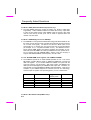
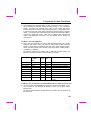
Appendix B
Frequently Asked Question
Note: FAQ may be updated without notice. If
you cannot find the information that you need in
this appendix, visit our WWW home page,
(address: http://www.aopen.com.tw) and check
the FAQ area and other new information.
Q: How can I identify the mainboard BIOS version?
A: The AOpen mainboard BIOS version appears on the upper-left corner of the
POST (Power-On Self Test) screen. Normally, it starts with R and is found
in between the model name and the date. For example:
AP53/AX53 R3.80 Oct.22.1996
BIOS revision
Q: How can I identify version of the mainboard?
A: The AOpen mainboard version appears as ppppp-x on the PCB, near the
PCI slot and is enclosed in a white bordered box. The ppppp is the project
code used by AOpen internally and -x is the version code. For example, for
AP5T with 95152 project code and -1 version code, the mainboard version
appears on the PCB as follows:
95152-1
AP5T MB
48.87901.011
MB verison -1
(AP5T-1)
B-1
Frequently Asked Questions
Q: Why the AOpen mainboards (MB) do not have cache module expansion
slot?
A: Faster CPU speed requires more difficult and complex MB timing design.
Every trace and components delay must be taken into consideration. The
expansion cache slot design will cause 2 or 3ns delay in PBSRAM timing,
and the extended trace length to the cache module through the golden finger
will further delay the timing by 1 or 2ns. This may result in unreliable system
once the cache module and slot becomes worn. All AOpen MBs support
512KB PBSRAM onboard. For better performance (around 3% higher than
256KB), we strongly recommend you to use 512KB onboard. Otherwise,
reliable 256KB is better than unreliable 512KB with cache module. AOpen is
the first company to promote this concept since the fourth quarter of 1995.
Q: What is MMX?
A: MMX is the new single-line multiple-instruction technology of the new Intel
Pentium PP/MT (P55C) CPU. A new Pentium Pro CPU (Klamath) with MMX
technology is also expected to be released soon. The MMX instructions are
specifically useful for multimedia applications (such as 3D video, 3D sound,
video conference). The performance can be improved if applications use
these instructions. All AOpen MBs have at least dual power onboard to
support PP/MT, it is not necessary to have special chipset for MMX CPU.
Q: What is USB (Universal Serial Bus)?
A: USB is a new 4-pin serial peripheral bus that is capable of cascading
low/medium speed peripherals (less than 10Mbit/s) such as keyboard,
mouse, joystick, scanner, printer and modem/ISDN.
With USB, the
traditional complex cables from back panel of your PC can be eliminated.
You need the USB driver to support USB device(s). AOpen MBs are all USB
ready, you may get latest BIOS from AOpen web site
(http://www.aopen.com.tw). Our latest BIOS includes the keyboard driver
(called Legacy mode), that simulates USB keyboard to act as AT or PS/2
keyboard and makes it possible to use USB keyboard if you don't have driver
in your OS. For other USB devices, you may get the drivers from your
device vendor or from OS (such as Win95). Be sure to turn off " USB
Legacy Support" in BIOS "Chipset Setup" if you have another driver in your
OS.
Q: What is P1394?
A: P1394 (IEEE 1394) is another standard of high-speed serial peripheral bus.
Unlike low or medium speed USB, P1394 supports 50 to 1000Mbit/s and can
be used for video camera, disk and LAN. Since P1394 is still under
development, , there is no P1394 device currently available in the PC
B-2
Frequently Asked Questions
market. Also, there is no chipset that can support P1394. Probably in the
near future, a card will be developed to support P1394 device.
Q: What is SMBus (System Management Bus, also called I2C bus)?
A: SMBus is a two-wire bus developed for component communication
(especially for semiconductor IC). It is most useful for notebook to detect
component status and replace hardware configuration pin (pull-high or pulllow). For example, disabling clock of DIMM that does not exist, or detecting
battery low condition. The data transfer rate of SMBus is only 100Kbit/s, it
allows one host to communicate with CPU and many masters and slaves to
send/receive message. The SMBus may be used for jumpless mainboard,
the components which support SMbus are not ready yet, we will keep eyes
on it.
Q: What is FCC DoC (Declaration of Conformity)?
A: The DoC is new certif ication standard of FCC regulations. This new standard
allows DIY component (such as mainboard) to apply DoC label separately
without a shielding of housing. The rule to test mainboard for DoC is to
remove housing and test it with regulation 47 CFR 15.31. The DoC test of
mainboard is more difficult than traditional FCC test. If the mainboard
passes DoC test, that means it has very low EMI radiation and you can use
any kind of housing (even paper housing). Following is an example of DoC
label. Currently, AOpen AX65/AP57/AP5T/AX5T had passed DoC test.
AX5T
Test To Comply
With FCC Standards
FOR HOME OR OFFICE USE
Q: What is PBSRAM (Pipelined Burst SRAM)?
A: For Pentium CPU, the Burst means reading four QWord (Quad-word, 4x16 =
64 bits) continuously with only the first address decoded by SRAM. The
PBSRAM will automatically send the remaining three QWord to CPU
according to predefined sequence. The normal address decoding time for
SRAM is 2 to 3 clocks. This makes the CPU data read timing of four QWord
to be at least 3-2-2-2 and a total of 9 clocks if traditional asynchronous
SRAM is used. However, with PBSRAM, there is no need to decode address
for rest three Qword. Therefore, data read timing can be 3-1-1-1, that is
equivalent to 6 clocks and is faster than asynchronous SRAM.
B-3
Frequently Asked Questions
Q: What is EDO (Extended Data Output) memory?
A: The EDO DRAM technology of EDO is actually very similar to FPM (Fast
Page Mode). Unlike traditional FPM that tri-states the memory output data
to start the pre-charge activity, EDO DRAM holds the memory data valid
until the next memory access cycle, that is similar to pipeline effect and
reduces one clock state.
Q: What is SDRAM (Synchronous DRAM)?
A: The SDRAM is a new generation DRAM technology that allows DRAM to use
the same clock as the CPU host bus (EDO and FPM are asynchronous and
do not have clock signal). The idea is the same as "Burst" (refer to the
previous Q & A). It requires only one clock for the 2nd, 3rd, and 4th QWord
(for example, 5-1-1-1 compares with EDO 5-2-2-2). The SDRAM comes in
64-bit 168-pin DIMM (Dual-in-line Memory Module) and operates at 3.3V.
Note that some old DIMMs are made by FPM/EDO and only operate at 5V.
Do not confuse them with SDRAM DIMM. AOpen is the first company to
support dual-SDRAM DIMMs onboard (AP5V), from Q1 1996.
Q: Can SDRAM DIMM work together with FPM/EDO SIMM?
A: The FPM/EDO operate at 5V while SDRAM operates at 3.3V. The current
MB design provides different power to DIMM and SIMM but connects the
data bus together. If you combine SIMM and DIMM, the system will still
work fine; however, only temporarily. After a few months, the SDRAM 3.3V
data input will be damaged by 5V FPM/EDO data output line. Therefore, we
strongly NOT recommend DIMM and SIMM combined together. There is one
exception, if your SDRAM supports 5V tolerance (such as TI or Samsung),
which accepts 5V signal at 3.3V operating power, you can combine them.
Manufacturer
Model
Samsung
NEC
Micron
TI
TI
KM416S1120AT-G12
D4516161G5-A12-7JF
MT4LC1M16E5TG-6
TMS626162DGE -15
TMS626162DGE M-67
Q: What is Bus Master IDE (DMA mode)?
B-4
Suggested CAS
Latency Time
2
2
2
2
3
5V Tolerance
Yes
No
No
Yes
Yes
Frequently Asked Questions
A: The traditional PIO (Programmable I/O) IDE requires the CPU to involve in
all the activities of the IDE access including waiting for the mechanical
events. To reduce the workload of the CPU, the bus master IDE device
transfers data from/to memory without interrupting CPU, and releases CPU
to operate concurrently while data is transferring between memory and IDE
device. You need the bus master IDE driver and the bus master IDE HDD to
support bus master IDE mode. Note that it is different with master/slave
mode of the IDE device connection. For more details, refer to section 2.3
"Connectors".
Q: What is the Ultra DMA/33?
A: This is the new specification to improve IDE HDD data transfer rate. Unlike
traditional PIO mode, which only uses the rising edge of IDE command
signal to transfer data, the DMA/33 uses both rising edge and falling edge.
Hence, the data transfer rate is double of the PIO mode 4 or DMA mode 2.
(16.6MB/s x2 = 33MB/s).
The following table lists the transfer rate of IDE PIO and DMA modes. The
IDE bus is 16-bit, which means every transfer is two bytes.
Mode
PIO mode 0
PIO mode 1
PIO mode 2
PIO mode 3
PIO mode 4
DMA mode 0
DMA mode 1
DMA mode 2
DMA/33
Clock per
33MHz
PCI
30ns
30ns
30ns
30ns
30ns
30ns
30ns
30ns
30ns
Clock
count
Cycle
time
Data Transfer rate
20
13
8
6
4
16
5
4
4
600ns
383ns
240ns
180ns
120ns
480ns
150ns
120ns
120ns
(1/600ns) x 2byte = 3.3MB/s
(1/383ns) x 2byte = 5.2MB/s
(1/240ns) x 2byte = 8.3MB/s
(1/180ns) x 2byte = 11.1MB/s
(1/120ns) x 2byte = 16.6MB/s
(1/480ns) x 2byte = 4.16MB/s
(1/150ns) x 2byte = 13.3MB/s
(1/120ns) x 2byte = 16.6MB/s
(1/120ns) x 2byte x2 =
33MB/s
Q: What is the performance of Ultra DMA/33? Do we need special driver?
A: You need driver to activate DMA/33, there are now driver from INTEL or you
can use driver in the Windows 95 Memphis, which can recognize South
Bridge PIIX4.
We got the mass production sample Quantum Fireball ST1.6A, following are
the test result.
B-5
Frequently Asked Questions
MB
CPU
DRAM
VGA
CDROM
OS
: AOpen AP5T
: P54C-200 Mhz
: 16MB * 2 (FP-7)
: AOpen PV60
: AOpen CD-920E (20X)
: Win95 OSR2
Model
OS/Driver
Mode
Quantum
Fireball 1.2G
Quantum
Fireball 1.2G
Quantum
ST1.6A
Quantum
ST1.6A
Windows 95 OSR2
PIO mode
4
DMA
mode 2
PIO mode
4
DMA/33
Windows 95 OSR2 +
INTEL PIIX4 driver
Windows 95 OSR2
Windows 95 OSR2 +
INTEL PIIX4 driver
Winbench97 Disk
Winmark
(Business)
717
Winbench97 Disk
Winmark (High
End)
2150
822
3050
853
2630
1040
4020
Q: What is PnP (Plug and Play)?
A:
In the past, the IRQ/DMA and memory or I/O space of add-on cards are
normally set manually, i.e., by jumper or by proprietary utility. The user has
to check the user's guide for the correct setting. Sometimes, resource
conflict occurs and this leads to unstable system. The PnP specification
suggests a standard register interface for both BIOS and OS (such as
Win95). These registers are used by BIOS and OS to configure system
resource and prevent any conflicts.
The IRQ/DMA/Memory will be
automatically allocated by PnP BIOS or OS.
Currently, almost all the PCI cards and most ISA cards are PnP compliant.
If you are still using a Legacy ISA card that cannot support PnP, set the
corresponding resource (IRQ/DMA/memory) to ISA in the BIOS "PCI/PnP
Setup".
Q: What is ACPI (Advanced Configuration & Power Interface) and OnNow?
A: The ACPI is new power management specification of 1997 (PC97). It
intends to save more power by taking full control of power management to
operating system and not through BIOS. Because of this, the chipset or
super I/O chip needs to provide standard register interface to OS (such as
Win97) and provides the ability for OS to shutdown and resume power of
different part of chip. The idea is a bit similar to the PnP register interface.
ACPI defines momentary soft power switch to control the power state
transition. Most likely, it uses the ATX form factor with momentary soft
power switch. The most attractive part of ACPI for desktop user is probably
the "OnNow" feature, an idea from notebook. This feature allows you to
B-6
Frequently Asked Questions
immediately resume to your original work without the long time waiting from
bootup, entering Win95 and running Winword. The AX5T with Intel TX
chipset can support ACPI.
Q: What is ATX Soft Power On/Off and Momentary Switch?
A: The Soft Power On of the ATX specification means to provide a standby
current for special circuit to wait for wakeup event when main power is off.
For example, Infrared wakeup, modem wakeup, or voice wakeup. Currently,
the most simple usage is to provide standby current for power switch circuit
so that power switch can turn on/off the main power through soft power
control pin. The ATX power specification does not mention anything about
the power switch type. You can use toggle or momentary switch, note that
ACPI specification requires momentary switch for power state control. All
the AOpen ATX MBs support momentary switch and AX5T/AX58/AX6L
support modem wakeup (Modem Ring-On).
Soft Power Off me ans to turn off system through software, Windows 95
Shutdown function can be used to verify if your mainboard supports soft
power off. AOpen AX5T/AX58/AX6F/AX6L support soft power off.
Q: What is the AGP (Accelerated Graphic Port)?
A: AGP is a PCI-like bus interface targeted for high-performance 3D graphic.
AGP supports only memory read/write operation and single-master singleslave one-to-one only. The AGP uses both rising and falling edge of the
66MHz clock and produces 66MHz x 4byte x 2 = 528MB/s data transfer rate.
The AOpen AX6L MB are designed to support AGP via the new Intel
Klamath LX chipset.
Q: Which Pentium chipset has the best performance?
A: The performance difference of chipset depends on what kind of DRAM they
use and the DRAM timing they support. (They all use PBSRAM, so that the
difference is very little at 2nd level cache.)
The following table lists the read timing of current available chipsets. The
four digital represents the clocks needed for 1st-2nd-3rd-4th QWord. Notice
that the Intel HX + EDO or SIS 5571+ EDO are almost the same as VX +
SDRAM and the TX + SDRAM has the best performance among Pentium
chipsets. Please note AP57 does not support SDRAM.
P5 Chipset
Model
PBSRAM
FPM
EDO
SDRAM
B-7
Frequently Asked Questions
Intel 430FX
Intel 430VX
Intel 430HX
Intel 430TX
SIS 5571
SIS 5582
AP5C/P
AP5VM/
AP5V
AP53/
AP5K/
AX53
AP5T/
AX5T
AP57
AP58/
AX58
3-1-1-1
3-1-1-1
7-3-3-3
6-3-3-3
7-2-2-2
6-2-2-2
NA
6-1-1-1
3-1-1-1
6-3-3-3
5-2-2-2
NA
3-1-1-1
6-3-3-3
5-2-2-2
5-1-1-1
3-1-1-1
3-1-1-1
5-3-3-3
5-3-3-3
4/5-2-2-2
4/5-2-2-2
(6/7-1-1-1)
6/7-1-1-1
Q: What is the memory performance improvement of TX chipset?
A: Following is the compare table of TX+SDRAM, VX+SDRAM, TX+EDO,
HX+EDO and VX+EDO.
CPU
DRAM
HDD
VGA
OS
: Pentium PP/MT (P55C) 200MHz
:16MB EDO or SDRAM
: Quantum Fireball 1280AT
: AOpen PV60 S3 Trio64V+ 800x600x256 Small font
: Windows 95 OSR2
Chipset
Model
DRAM
Timing
Intel 430VX
Intel 430HX
Intel 430TX
Intel 430VX
Intel 430TX
AP5VM
AP53/AP5K
AP5T/AX5T
AP5VM/AP5V
AP5T/AX5T
EDO
EDO
EDO
SDRAM
SDRAM
6-2-2-2
5-2-2-2
5-2-2-2
6-1-1-1
5-1-1-1
Winstone9
6
86.1
86.8
87.3
86.6
87.7
Q: Does Pentium or Pentium Pro MB support Deturbo mode?
A: The Deturbo mode was originally designed to slow down CPU speed for old
applications (especially old games). It uses programming loop to wait or
delay special event. This programming method is considered very bad since
the delay of loop highly depends on the CPU speed and the application fails
at high-speed CPU. Almost all new applications (including games) use RTC
or interrupt to wait event. There is no need for Deturbo mode now. The
Turbo switch is now used as Suspend switch. However, some MBs still
support Turbo/Deturbo function via keyboard. You can set the system to
B-8
Frequently Asked Questions
Deturbo by pressing <Ctrl> <Alt> <->. To back to Turbo mode, press <Ctrl>
<Alt> <+>. Note that the Deturbo mode has been removed in new MBs since
these require more code space in Flash ROM.
Q: Power Management Icon does not appear in the Windows 95 Control Panel
even though the APM under BIOS Setup is enabled.
A: This problem occurs if you did not enable the APM function before you install
Windows 95. If you have already installed Windows 95, re-install it after the
BIOS APM function is enabled.
Q: Why does the system fail to go into suspend mode under Win95?
A: This problem may be caused by your CDROM settings. The CDROM Auto
Insert Notification of Win95 is dafault enabled, the system will continue to
monitor your CDROM, auto-execute application when a CD diskette is
loaded, and prevents the system from entering into suspend mode. To
resolve this, go into Control Panel
System
Device Manager
CDROM
Setting, and disable the "Auto Insert Notification" function.
Q: What is Windows 95 Registry?
A: The functions of Windows 95 Registry and the Windows 3.1 INI files are
almost the same. Both store the hardware and software configurations. The
only difference is that Registry is a database while INI is text file. You can
run REGEDIT.EXE to further understand the Registry structure. Checking
and studying the structure of this file will help you solve some configuration
problems.
Q: Why are there question marks or "standard IDE controller" presented
under Device Manager after installing Win'95 on AP5T/AX5T based
system?
A: Intel has introduced 430TX chipset with latest feature of "ACPI", "USB" &
"Ultra DMA/33". Since these devices are so new that Win'95 did not
anticipate to support them on Aug. of '95 which Win'95 initially is being
released. Under Win'95 Device Manager, you may see following devices
installed:
-Other Devices
? PCI Bridge
? PCI Card (or PCI Universal Serial Devices)
-Hard Disk Controllers
Standard Dual PCI IDE Controller
B-9
Frequently Asked Questions
Primary IDE Controller
Secondary IDE Controller
PCI Bridge:
This device stands for the "ACPI" feature which implemented within
PIIX4(82371AB) chipset. This new feature is expected to be fully utilized
under Windows'97(Memphis). Please look for more details on ACPI from
FAQ "What is ACPI?".
PCI Card:
There is driver ne cessary in order to support Universal Serial Device under
Win'95. Microsoft has implemented the driver since
Win'95 OEM Service
Release 2.1 (OSR 2.1) & it will recognize USB port without any problem.
Pleae contact your USB device vendor or system vendor of more
inforamtion. Also, more details for USB in the FAQ of "What is USB?".
Standard Dual PCI IDE Controller:
The IDE controller chipset -- PIIX4 -- will be fully recognized under
Windows'97 also. In the mean while, you may download the
driver for
Win'95 from AOpen homepage at "http://www.aopen.com.tw" which supports
both Bus Mastering & Ultra DMA/33. After installation, you should be able to
see Win'95 recognize it under Device Manager as below:
-Hard Disk Controllers
Intel 82371AB PCI Bus Master IDE Controller
Primary Bus Master IDE Controller
Secondary Bus Master IDE Controller
Even though all of above are the current limitations of Win'95 on Intel 430TX
chipset which are expected to implement on Win'97, your system still can
enjoy the best performance of AP5T/AX5T without any problem.
Q: Which version of the Windows '95 that I am using?
A: You may determine the version of Windows '95 by following steps.
1. Double click "System" in "Control Panel".
2. Click "General".
3. Look for "System" heading & refer to following,
4.00.950
4.00.950A
B-10
Windows 95
Windows 95 + Service Pack or OEM Service Release 1
Frequently Asked Questions
4.00.950B
OEM Service Release 2 or OEM Service Release 2.1
If you are running OSR 2.1, you may tell it from by check ing "USB
Supplement to OSR2" in the list of installed program of Add/Remove
program tool under Control Panel, and checking for version 4.03.1212 of the
Ntkern.vxd file in the Windows\System\Vmm32 folder.
Q: What is the difference between AX5T-1 and AX5T-2?
A: AX5T-2 fixes the ATX power supply to off state when you first time install
your AX5T mainboard. AX5T-1 can be probably on or off. Note that currently,
they all have 75MHz but without 83.3Mhz jumper setting because of clock
generator limitation. The user set clock to 75MHz is taking his own risk, and
is probably to have system unstable behavior.
Item
75MHz jumper setting
83.3MHz jumper setting
ATX Power Supply initial
state
AX5T-2
Yes
No
Off
AX5T-1
Yes
No
Random
Q: What is the difference of Linear Regulator and Switching
Regulator?
A: Switching regulator turns on/off Power FET with very high frequency and
uses L/C charge and discharge circuit to do voltage drop. The efficient is
better but voltage ripple and EMI noise is higher. The reason for mainboard
designer to consider switching regulator, is simply because they are worry
about linear regulator can not fully support the coming new CPU. Actually,
this depends on the design and layout quality of mainboard manufacturer.
According to AOpen RD's testing, Intel PP/MT-233, AMD K6-166/200/233
are all fine on AP5T to run winstone97. (The CPU is at 53 degree C, heatsink
is at 60 degree C and regulator IC is at 79 degree C). But for future CPU
(perhaps CPU of 1998), AOpen will still consider to phase-in switching
regulator on new version mainboard.
Q: What is the performance improvement of AMD K6?
A: Following is the compare table of the new generation CPU.
DRAM : 64MB EDO
HDD : Quantum Fireball 1280AT
VGA
: Matrox Millennium VGA, 4MB, 1024x768 24bit, 85Hz.
B-11
Frequently Asked Questions
OS
: Windows 95 4.00.950
CPU
MB
Chipset
Winstone97 Winstone97
Business
High-End
PP/MT 200
PP/MT 233
K6 PR200
* K6 PR210
(83.3MHz x 2.5)
K6 PR233
* K6 PR250
(83.3MHz x 3)
AP5T/AX5T
AP5T/AX5T
AP5T/AX5T
AP5T
Intel 430TX
Intel 430TX
Intel 430TX
Intel 430TX
48.3
50.5
50.3
51.2
21.9
23.6
22
23
AP5T/AX5T
AP5T
Intel 430TX
Intel 430TX
51.7
54
23.6
24.8
You can see that K6-233 is better than PP/MT-233 on Business Winstone97,
but the High-End graphic Winstone97 is almost the same.
Note that, if you over-clock K6 to 250M (83.3MHz*3), it could be the fastest
socket -7 system among all. But please be reminded, it is your own risk to
over-clock
Q: When can we have real jumperless mainboard?
A: PnP had achieved the goal of jumperless add-on card, but true jumperless
mainboard still has some technical concerns. For example, CPU clock and
voltage do not have standard interface. Currently, the so called jumperless
mainboard is actually depends on the BIOS to detect or manually set the
CPU clock and voltage. If the setting is wrong, it will cause system unstable
or damage after long time use. The other disadvantage is, because some of
the jumper setting information is stored in CMOS, if the battery is lost or
BIOS setup is accidentally changed, end user (or distributor) may need to
open the housing and check the CPU again.
Most of all, you need a start voltage to boot CPU and go into BIOS for
jumperless setting. 2.85V may be OK for P55C and K6-166, but minimum
voltage of K6-233MHz is 3.1V, it can not boot if user plugs K6-233 onto
current jumperless mainboard.
We probably need to wait after the mature of SMbus, if CPU and clock
generator and other ICs are all SMbus compliance. Chipset can then detect
and report the system configuration right after power on. Then we can have
true jumperless mainboard.
Q: What is LDCM (LAN Desktop Client Manager)?
B-12
Frequently Asked Questions
A: This is a software of Intel. The major goal is to provide an easy way for
corporate network administrator to monitor the status of all the clients
(workstation). You need at least DMI BIOS for LDCM. AOpen BIOS is also
DMI ready but unfortunately, Intel LDCM needs Intel network card to work
properly. It is obviously not suitable for home user to pay LDCM extra cost.
B-13