1
APPENDIX
A1.1.1.1 - Readout Sequence of a CCD
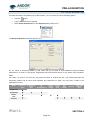
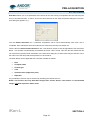
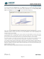
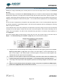
In the course of readout, charge is moved vertically into the shift register, and then horizontally from the shift
register into the output node of the amplifier. The readout sequence illustrated below (which corresponds to the
default setting of the Full Resolution Image binning pattern) allows data to be recorded for each individual
element on the CCD-chip. Other binning patterns are achieved by summing charge in the shift register and/or
the output node prior to readout. See Vertical & Horizontal Binning on pages 156- 158.
1
Exposure to light causes a pattern of charge (an electronic image) to build up on the frame (or ‘‘image
area’) of the CCD-chip.
2
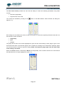
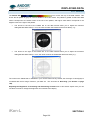
Charge in the frame is shifted vertically by one row, so that the bottom row of charge moves into the shift
register.
3
Charge in the shift register is moved horizontally by one pixel, so that charge on the endmost pixel of the
shift register is moved into the output node of the amplifier.
4
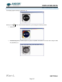
The charge in the output node of the amplifier is passed to the analog-to-digital converter and is read out.
5
Steps 3 and 4 are repeated until the shift register is emptied of charge.
6
The frame is shifted vertically again, so that the next row of charge moves down into the shift register.
The process is repeated from Step 3 until the whole frame is read out.
iKon-L
APPENDIX
Page 155