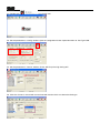
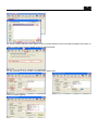
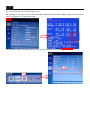
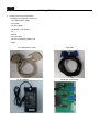
1
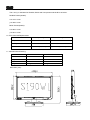
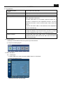
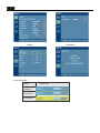
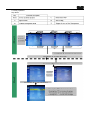
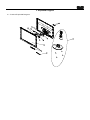
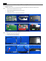
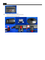
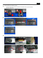
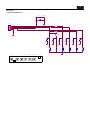
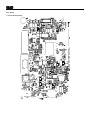
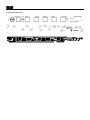
ACER_LCD_S190WL _SM20110519V0 Contents Table of Contents Important Safety Notice .............................................................................................................................. 1 1. Product Specification .............................................................................................................................. 2 2. OSD Menu ............................................................................................................................................ 16 3. Exploded Diagram ................................................................................................................................ 20 4. Assembly and Disassembly Procedures .............................................................................................. 23 5. Troubleshooting .................................................................................................................................... 29 6. Firmware Upgrade Process .................................................................................................................. 33 7. Writing EDID Process ........................................................................................................................... 39 8. FRU (Field Replaceable Unit) List ........................................................................................................ 45 9. Schematics and Layouts ...................................................................................................................... 48 Safety Notice Any person attempting to service this chassis must familiarize with the chassis and be aware of the necessary safety precautions to be used when serving electronic equipment containing high voltage. 1 Important Safety Notice Product Announcement: This product is certificated to meet RoHS Directive and Lead-Free produced definition. Using approved critical components only is recommended when the situation to replace defective parts. Vender assumes no liability express or implied, arising out of any unauthorized modification of design or replacing non-RoHS parts. Service providers assume all liability. Qualified Repairability: Proper service and repair is important to the safe, reliable operation of all series products. The service providers recommended by vender should being aware of notices listed in this service manual in order to minimize the risk of personal injury when perform service procedures. Furthermore, the possible existed improper repairing method may damage equipment or products. It is recommended that service engineers should have repairing knowledge, experience, as well as appropriate product training per new model before performing the service procedures. NOTICE: ! To avoid electrical shocks, the products should be connect to an authorized power cord, and turn off the master power switch each time before removing the AC power cord. ! To prevent the product away from water or explosed in extremely high humility environment. ! To ensure the continued reliability of this product, use only original manufacturer’s specified parts. ! To ensure following safety repairing behavior, put the replaced part on the components side of PWBA, not solder side. ! To ensure using a proper screwdriver, follow the torque and force listed in assembly and disassembly procedures to screw and unscrew screws. ! Using Lead-Free solder to well mounted the parts. ! The fusion point of Lead-Free solder requested in the degree of 220°C. 2 1. Product Specification 1.1 Scope: LCD BM190WX2-TJA1 LM190WX2-TJA1 is a Color Active Matrix Liquid Crystal Display with an integral Light Emitting Diode (LED) backlight system. The matrix employs a-Si Thin Film Transistor as the active element. It is a transmissive type display operating in the normally white mode. It has a 23.0 inch diagonally measured active display area with WXGA+ resolution (900 vertical by 1440 horizontal pixel array) Each pixel is divided into Red, Green and Blue sub-pixels or dots which are arranged in vertical stripes. Gray scale or the brightness of the sub-pixel color is determined with a 8-bit gray scale signal for each dot, thus, presenting a palette of more than 16,7M colors with Advanced-FRC(Frame Rate Control). It has been designed to apply the interface method that enables low power, high speed, low EMI. FPD Link or compatible must be used as a LVDS(Low Voltage Differential Signaling) chip. It is intended to support applications where thin thickness, wide viewing angle, low power are critical factors and graphic displays are important. In combination with the vertical arrangement of the sub-pixels, the LM190WX2-TJA1 characteristics provide an excellent flat panel display for office automation products such as monitors. General display parameters: 3 Optical Characteristics: 4 1.2 General Requirements: 1.2.1 Test Condition: All tests shall be performed under the following conditions, unless otherwise specified. Warm up time > 30 min. AC supply voltage 230V± 5%, 50± 3 Hz Ambient temperature 20C 5C Humidity Display mode 65% 20% 1440 x 900, 60 Hz, Pixel Clock:106.5MHZ,all white e-color mode Set to “User” mode Contrast control Set to The value under user mode, which allows that the brightest two of 32 linear distributed gray-scales (0~ 700mv) can be distinguished. Color temperature 6500°K Brightness control The value under user mode Analog Input signal 700 mVss Picture position and size Factory preset value, Viewing angle 90 ° H and V Viewing distance 40 cm for LCD performance, 20 cm for LCD failures Ambient illumination Dark room (< 1 cd/m2) 1.2.2 Test Equipment: CHROMA 6630. 1.3 Electrical: This section describes the electrical requirement of the monitor. Below is the block diagram. Flat Panel and Led drive LED backlight RS232 Connector Main Board For white balance adjustment in factory mode Key Board 19V AC-IN Adapter 100V-240V HOST Computer Video signal, DDC 5 The LCD monitor will contain a main board and a key board which house the flat panel control logic, brightness control logic and DDC. The adapter will provide AC to DC voltage to drive the main board chips each voltage. The function key board is used for OSD control, monitor power ON/OFF and the LED indicator for power status. LCD Panel Input Driving system TFT Color LCD Pixel pitch 0.2835 (H) x 0.2835 (V) (mm) Contrast Ratio 1000 (Typ.) Response time 5ms (Typ.). 10ms(max) Luminance of White 250 cd/m2 (Typ.) Separate Sync. H/V TTL H-Frequency 31kHz-80kHz V-Frequency 56-75Hz Viewing angle CR>10 ,R/L 170(Typ.), U/D 160(Typ.) Display mode 1440 x 900@60Hz EPA ENERGY STAR® Power Source ON Mode < 30W OFF Mode < 2W 100 V ~ 240 V, 50 3Hz, 60 3Hz Operating Temp: 0° to 40°C Storage Temp: -20° to 60°C Environmental Operating Humidity: 15% to 90% Considerations Storage Humidity: 15% to 90% Operating Altitude: 12,000 feet Storage Altitude: 40,000 feet Peak surge current Power line surge < 55A peak at 240 VAC and cold starting No advance effects (no loss of information or defect) with a maximum of 1 half-wave missing per second 6 1.3.1 Interface Connectors: 1.3.1.1 Power Adaptor and Connector: The AC inlet connector shall be an IEC 320-C13 male power receptacle for connection to mains power. The power cord shall be gray or black with length of 1.8m + 10cm/-0cm. The power cord type is different from regions.The adapter output cable length of 150036mm,voltage is 19v and current is 1.58A. 1.3.1.2 Analog Connector and Cable: The analog signal cable shall be Gray or black and 1.8m + 10cm/-0cm. A. D - S U B B. DVI(only for S190WL BD) 7 C. LED backlight Connector Connector: CN803 Pin Signal Pin Signal 1 Feedback1 7 LED drive 2 NC 8 NC 3 NC 9 NC 4 NC 10 Feedback2 5 NC 11 GND 6 LED drive 12 GND D. Key Board Connector Connector: CN401 Pin Signal Pin Signal 1 GND 4 POWER KEY 2 LEDA 5 KEY2 3 LEDG 6 KEY1 E. Flat Panel Connector Connector: CN407 Pin Signal Pin Signal 1 GND 26 GND 2 CLK1 27 ICLK_RESET 3 CLK1 28 H2DOT 4 CLK2 29 CSC 5 CLK2 30 POL 6 CLK3 31 POL2 7 CLK3 32 SOE 8 CLK4 33 GND 9 CLK4 34 LV0+ 10 GVDD_O 35 LV0- 11 GVDD_E 36 LV1+ 12 G_RES 37 LV1- 13 VGL 38 LV2+ 14 VGL 39 LV2- 15 VGH 40 GND 16 VGH 41 LCLK+ 17 VDD 42 LCLK- 18 VDD 43 GND 19 VDD 44 LV3+ 20 VCC 45 LV3- 21 VCC 46 LV4+ 22 VCOMD 47 LV4- 23 VCOMD 48 LV5+ 24 VCOMC 49 LV5- 25 VCOMC 50 GND 8 1.3.2 Input Signals: Video Input Signals Range (Analog RGB Signal) No. Symbol Item M in Max Unit 1 Fh Horizontal Frequency 31 80 kHz 2 Fv Vertical Frequency 56 75 Hz 3 Fclk Pixel Clock Frequency 106.5 MHz 4 5 Vih Vil High Level Input Low Level Input 2.4 0 0.8 V V 6 Video RGB Analog Video Level 0 0.7 V 1.3.2.1 Video Signal Amplitudes: The video inputs consist of Red, Green and Blue signals each has its own coaxial cable terminated at the monitor. These video signals are analog levels, where 0V corresponds to black, and 700mV is the maximum signal amplitude for the respective color. The video signal is terminated with 75 ohms. 1.3.2.2 Video Signal Termination Impedance: The analog video signal termination shall be 75 ohm. 1.3.2.3 Synchronization (Sync) Signals: The Horizontal Sync (HS) TTL signal is used to initiate the display of a horizontal line. HS may be either active high or active low according to the timing. The Vertical Sync (VS) TTL signal is used to initiate the display of a new frame. VS may be either active high or active low according to the timing. 1.3.2.4 Sync Signal Levels: Level: L = 0V ~ 0.8V H = 2.4V ~ 5V 1.3.2.5 Abnormal Signal Immunity: The monitor shall not be damaged by improper sync timing, pulse duration, absence of sync, abnormal input signal amplitude, or any other anomalous behavior of a graphics card. 1.3.2.6 Digital TMDS Input (DVI signal input): 1.3.3 User Controls and Indicators: Signals used for mode detection: -Nominal horizontal frequency -Nominal vertical frequency -Horizontal sync. Pulse polarity -Vertical sync. Pulse polarity The tolerance for detecting the horizontal frequency is between ±1KHz from center frequency The tolerance for detecting the vertical frequency is between ±0.5Hz from center frequency 1.3.3.1 Power On/Off Switch: The monitor shall have a power control switch visible and accessible on the front of monitor. 9 1.3.3.2 Power Indicator LED: The monitor shall have LED indicators located on the front of the monitor. Table 1 is the LED color for the power indicator. 1.3.3.3 On-Screen Display: On Screen Display system shall be used to control the monitor. Current setting will be saved and OSD will be tuned off when the keys are not touched for a period of time. A) Key Function Overview: All functions are controlled by OSD buttons on the front of bezel. 1. Power Switch To turn ON or OFF the power. 2.Power LED Lights up to indicate the power is turned ON. 3.Empowering Trigger the acer eColor Management. 4.Auto Adjust button / Exit 1) When OSD menu is in active status, this button will act as EXIT-KEY (EXIT OSD menu). 2) When OSD menu is in off status, press this button for 2 seconds to activate the Auto Adjustment function .The Auto Adjustment function is used to set the Hpos, Vpos, Clock and Focus. 3) When exit eColor OSD, it will activate the Auto Adjustment function automatically. 5.< / > Press < or > to select the desired function. Press < or > to change the settings of the current function. Or press < to trigger volume management OSD, press > to change input source. 6.MENU / ENTER Activate OSD menu when OSD is OFF or activate/de-activate adjustment function when OSD is ON. But it has no function at the information page. 10 B) Menu Operation: Pressing the MENU button brings up the first level menu. C) OSD Function: Acer e-Color Management Contrast, Brightness, ACM H-position, V-position Clock, Focus OSD position, Timeout Color Select and adjust (warm, cool, user). EMEA:11 Language selected (English, Deutsch, French, Spanish, Italian, Hollands, Finnish, Turkish, Polish, Pусский, Portuguese ) ASIA: 8 Language selected (English, DutSch, French, Spanish, Italian, Japanese, Chinese, Chinese Simplify, ) Signal Input Select and DDC/CI Control (Analog, DDC/CI) Display Information Factory Reset Exit D) OSD Control Factory Default Values: eColor mode Standard Brightness 100 Contrast 50 ACM Off Color Warm Language English OSD Timeout 10s DDC/CI On User R/G/B 50/50/50 1.3.4 Monitor Modes and Timing Capability: 1.3.4.1 Format and Timing: The monitor shall synchronize with any vertical frequency from 56 to 75 Hz, and with any horizontal frequency from 31 to 80 KHz. 11 1.3.4.2 Factory Assigned Display Modes: 1.4 Flat Panel: 1.4.1 General Requirements: The panel shall be a FULL HD resolution 19” diagonal TFT-LCD. 1.4.2 Polarizer Hardness: The front polarizer should have hard coating (3H) and anti-glare treatment. 1.4.3 Backlight Requirements: 12 1.4.3.1 General Requirements: Parameter Symbol Condition Values Min. Typ. Max. Unit LED : LED String Current Is - 60 65 mA LED String Voltage Vs - 51.2 56 V PBar - 9.2 10.1 Watt LED_LT 30,000 - Hrs Power Consumption LED Life Time - 1.4.4 Defects: 1.4.4.1 Defect Terminology: Dark Spots / Lines: Spots or lines that appear dark in the display patterns and are usually the result of contamination. Defects do not vary in size or intensity (contrast) when contrast voltage is varied. Contrast variation can be achieved through the use of varying gray shade patterns. Bright Spots / Lines: Spots or lines that appears light in the display patterns. Defects do not vary in size or intensity (contrast) when contrast voltage is varied. Contrast variation can be achieved through the use of varying gray shade patterns. Polarizer Scratch: When the unit lights, lines appear light (white) with display patterns dark and do not vary in size. Physical damage to the polarizer does not damage the glass. Polarizer Dent: When the unit lights, spots appear light (white) with display patterns dark and do not vary in size. Physical damage to the polarizer does not damage the glass. Rubbing Line: Horizontal or diagonal lines that appear gray with the display patterns dark and may have resulted from an “out of control” rubbing process on the polyimide or “waves” on the BEFs or prism sheets . Newton Ring: The “rainbow” effect caused by non-uniform cell thickness. Mottling: When the unit lights, variation / non - uniformity (splotch) appears light (white) with the display and might vary in size. Dim Line: When the unit lights, line(s) in the minor (vertical) or major (horizontal) axis appear dim, but not completely on or off. Cross Lines Off: When the unit lights , lines in both the minor and major axis do not appear. Bright/Dark Dot: A sub - pixel (R, G, B dot) stuck off / on (electrical). 1.5 Optical Characteristics: 1.5.1 Brightness uniformity: Definition of White Variation (δW): 13 Surface luminance is the luminance value at center 1 point(1) across the LCD surface 50cm from the surface with all pixels displaying white. For more information see FIG 8. The variation in surface luminance , WHITE is defined as Minimum (P1,P2 …..P9) WHITE = --------------------------------------------- *100 Maximum (P1,P2 …..P9) For more information see Figure 8. 1.5.2 Contrast ratio (CR): 1.5.2.1 General CR: The values specified are at an approximate distance 50cm from the LCD surface at a viewing angle of and equal to 0 °. Contrast ratio(CR) is defined mathematically as :It is measured at center point(1) Surface luminance with all white pixels Contrast ratio = --------------------------------------------------------Surface luminance with all black pixels 14 1.5.3 Response time: Response time is the time required for the display to transition from black to white (Decay Time, TrD) and from white to black (Rise Time, TrR) The sampling rate is 2,500 sample/sec. For additional information see FIG. 9. The response time is defined as the following figure and shall be measured by switching the input signal for each gray to gray. 1.5.4 Viewing angles: Viewing angle is the angle at which the contrast ratio is greater than 10 or 5. The angles are determined for the horizontal or x axis and the vertical or y axis with respect to the z axis which is normal to the LCD surface. For more information see FIG. 8. 15 1.5.5 Chromaticity: The x and y co-ordinates for Reddish, Bluish and User preset mode shall be as below: Reddish Preset (6500K): x=0.313 ± 0.020 y=0.329 ± 0.020 Bluish Preset (9300K): x=0.283 ± 0.020 y=0.297 ± 0.020 1.6 Environmental Requirements: Operating Storage Temperature: 0°C - +40°C -20°C - +60°C Humidity: 15% - 90% 15% - 90% Altitude: 12,000 feet (3,658m) 40,000 feet (12,192m) 1.7 Mechanical and Packing: Monitor Packed Monitor Width: 377.8mm 425 Height: 296.1mm 300 Depth: 160.3mm 110 Weight: 1.7kg 2.4kg Dimension (mm): 16 2. OSD Menu 2.1 Key Definition: 1. Power Switch To turn ON or OFF the power. 2.Power LED Lights up to indicate the power is turned ON. 3.Empowering Trigger the acer eColor Management. 4.Auto Adjust button / Exit 1) When OSD menu is in active status, this button will act as EXIT-KEY (EXIT OSD menu). 2) When OSD menu is in off status, press this button for 2 seconds to activate the Auto Adjustment function. The Auto Adjustment function is used to set the Hpos, Vpos, Clock and Focus. 3) When exit eColor OSD, it will activate the Auto Adjustment function automatically. 5.< / > Press < or > to select the desired function. Press < or > to change the settings of the current function. Or press < to trigger volume management OSD, press > to change input source. 6.MENU / ENTER Activate OSD menu when OSD is OFF or activate/de-activate adjustment function when OSD is ON. But it has no function at the information page. 2.2 Function Menu: 1). Display Function Menu while user press any function button. 2). Layout as following figure: 2.3 Main OSD Menu: 2.3.1. OSD layout: a. Display OSD menu when user press “MENU” button on front bezel. b. Layout as following figure. c. OSD layout for each function page. 17 Picture OSD Setting Information d. Item page status Status Non-Focus Item focused Item selected Display type 18 2.3.2 Key operation: Key define: 19 2.4 Acer eColor management: a. Display Acer eColor Management OSD when user press “e” button at Function menu or trigger this function in OSD menu/picture page. b. Layout as following figure: 2.5 OSD Message: 20 3. Exploded Diagram 3.1 Product Exploded Diagram: 21 Note: The parts information listed below are for reference only, and are subject to change without notice. Please go to http://cs.tpv.com.cn/hello1.asp for the latest information. S190WL b Item Description LNT Part No. Acer Part No. 1 BEZEL ASSY A34G2642AEMA1B0130 60.LUF0B.001 2 KEY BOARD KEPCBQJ1 55.LUF0B.002 3 BM190WX2-TJA1-7F1-A0 FQ LTD 750GBT190W2A11N000 LK.19008.039 4 MYLAR F52G18014D8001 N/A 5 MAIN BOARD CBPCBAWABQJ 55.LUF0B.001 6 I/O BRACKET A15G1677101 N/A 7 REAR COVER ASSY A34G2643AEMA1B0100 60.LUF0B.002 8 HINGE ASSY A37G0268011 60.LUF0B.003 S1 SCREW(MAIN BOARD TO IO BRACKET) 0M1G1730--6120 N/A S2 SCREW(REAR COVER TO IO BRACKET) 0M1G-130--8-47-CR3 N/A S3 PCB SUPPORT(MAYLAR TO MAIN BOARD) Q11G0108--1 N/A 22 3.2 Packing Exploded Diagram: ITEM DESCRIPTION QT'S 1 2 3 4 5 6 7 8 9 10 11 12 13 14 15 16 CARTON EPS-1 EPS-2 EPE BAG FOR MONITROT HEAR OF MONITOR PE BAG FOR BASE BASE PE BAG FOR STAND STAND POWER CABLE SIGNAL CABLE QSG WARRANTY CARD ENERGY STAR CARD CD MENUAL ADAPTER 1 1 1 1 1 1 1 1 1 1 1 1 1 1 1 1 23 4. Assembly and Disassembly Procedures 4.1 Assembly Procedures: S1 Prepare a main board, an I/O Bracket and a Mylar. Assemble every part as the below picture. ① Turn over the main board and Lock screw. ② Turn over the main board and lock the four screws. ③ Paste the AL tape ④ Assemble the mylar on the back of main board. 4 3 2 1 S2 Prepare a bezel, a key board and a panel. ① Assemble the bezel and Keyboard. ② Put the panel in the bezel assembly. 1 24 2 S3 S3 Connect FFC cable and fix Mainboard: ① Connect panel pcb and main board with FFC cable ② Paste the tape. ③ Follow the two marks to fix the main board on the back cover and then paste the AL tape. 1 2 Mark 3 Mark Mark S4 Connect the all cable and the paste all tapes as the below picture: 25 S5 Assemble rear cover and lock the two screws. S6 Prepare a Stand, a Hinge and a Base. ① Assemble the stand and hinge, lock the two screws ② Assemble the stand ass’y and the base 1 2 26 4.2 Disassembly procedures: S1 Put the monitor on a protective cushion. ① Press the release button follow arrowhead as the below picture to remove the base. ② Pull out the stand ass’y. 2 1 S2 Unscrew the two screws and then open all latches with tool. S3 Remove the rear cover. S4 Tear out all tapes on panel. 27 S5 Disconnect two FFC cables and Key board cable as the below picture: S6 Separate the main board and I/O Bracket. ① Turn over the main board and take out the mylar. ② Turn over the main board and unscrew the four screws, then tear out the AL tape. ③ Unscrew the screw. 1 2 3 28 S7 Remove the panel. S8 Separate the key board and the bezel. 29 5. Troubleshooting 1. No Power No power Check power cable is tightened or adapter is ok? NG Re-plug the power cable or replace the adapter OK Check Power “On/Off” NG Turn on the Power “On/Off” switch is “On”? OK Check the LED indicate is OK? OK Replace the power board and check connections NG Replace main board and check connections NG Replace key board and check connections NG Check the AC power 30 2. No Video (Power LED Blue) No Video (Power LED Blue) Press the power NG Replace the main board button is OK? OK Check the main board NG Re-plug the cable and connection OK Check the LVDS/FFC cable or panel NG Replace the key board OK Replace the LVDS/FFC cable or panel 31 3. DIM DIM (image overlap, focus or flicker) Reset in factory mode OK The end NG Set to the optimal frequency, select the recommended frequency OK The end NG Readjust the phase and pixel OK The end clock in the user mode NG Pull out signal cable and check “Self Test Feature Check” is ok? NG OK Check the signal cable and the PC NG OK Replace the main board NG Replace the panel OK The end 32 4. Color is not optimal Color is not optimal Color shift Miss color Reset the factory mode Replace the signal cable NG OK NG The end In the user mode, set the” color settings” until customer satisfy Pull out the signal cable and check the screen color display is normal? NG OK NG Replace the signal cable or PC Replace the main board 33 6 Firmware Upgrad 6. de Process s 6.1 1 Test Envirronment Pre eparation: Hardware e and Softwa are Require ed: - USB cab ble - VGA cab ble - ISP Boarrd: 715GT034-B - PC - Monitor - ISP tool: V4.5.0.8.0 - New F/W W USB cable V VGA cable ISP P Board: 715 5GT034-B PC Monito or ISP P tool: V4.5.0 0.8.0 34 New F/W 6.2 Connection: 6.3 ISP Programming Procedures: S1. These three files must be put in one folder as the below picture. 35 S2. Double-click to run the ISP tool. S3. Set the parameters in “Config” window. Open the configration window. Speed less than 39. Port Type:USB. S4. Set the parameters in “Device” window. Check “WP Pin pull to high during ISP”. S5. Click the “Connect”, the tool will communicate with monitor which can detect the flash type. 36 S6. Load the F/W as the below picture. S8. Set the restore address to save HDCP for DVI or HDMI. Deferent monitor has deferent address and space for HDCP. If monitor has not DVI or HDMI, don’t tick “Restore Enable”. S9. Set parameter in “Auto” window. Processing after clicking “Run”. S10. Successful upgrade. 37 6.4 Check the firmware version. S1. Connect VGA source to monitor and turn it on. S2. Pressing “e” and power on, when the screen lights, release the key and press “MENU” again to open the menu with “F” and select “F” to open factory menu. Check this F/W version. S3. Restart the monitor. And then open the user menu. Factory reset will turn off Burn in mode. 38 6.5 Q&A S1. If appear Enter ISP Fail as the below left picture. Check the cables and ISP board whether are connected fluently. If not ok, AC off the monitor for a while and retry it. Click the “Dis Con” and click “Connect” again (as below right picture). S2. If appear Blank Error. Change ISP board or cable. Make sure the connection is ok. Change PC. S3.If appear Auto Detect error! The disconnection of ISP Board results this error. Please check the ISP board connection with PC. 39 7. Writing EDID Process 7.1 Test Environment Preparation: Hardware and Software Required: - LPT cable(male to male) - VGA cable -12V DC adapter - ISP Board: 715GT034-B - PC - Monitor - LPT port driver - ISP tool: TPVDDC20100901.exe - EDID LPT cable(male to male) 12V DC adapter VGA cable ISP Board: 715GT034-B 40 P PC Monitor LPT port driver d PVDDC2010 00901.exe ISP tool: TP D EDID 41 7.2 Connection: 7.3 Writing VGA and DVI Process: S1.Double-click to install it. And restart PC after installation. S2. Prepare the EDID written. Change the EDID files name as below rule. Anolog EDID Digital EDID Wa.dat Wd.dat S3. Copy WA.dat to one folder named as ACER S190WL which must contains “config.ini” file. S4. Copy ACER P166HQL to DDC folder and put DDC and ISP tool together. 42 S5. Double-click the icon to open the tool. S6. Check the “Analog+DVI” and click “Loadfile” to set the parameters. Click “Analog”and“Digital”, Manufacturer: ACR, Product Code: 0293,Model Name: ACER S190WL. 2 1 4 3 S7. Select the EDID folder as the below picture. 2 1 43 S8. Load EDID successful. S9. Check the Only connect VGA” and “Write SN”, and type in the 22 digit S/N which must be the same as S/N in the monitor’s barcode. 1 2 3 S10. Click “Program” to start writing. When the green “PASS” appear, the process is finished. 44 7.4 Check the S/N. S1. Press “MENU” key —“ ”— “Information”—“SN” in user mode. 7.5 Q&A S1. If can’t write! You could try to restart the monitor (AC on the monitor and turn on it). S2. If can’t write! Take apart the monitor and connect the 7pin of EEPROM to GND to diable write protection then write EDID one by one. S3. If can’t write! Set the Burn in on last to try again. 45 8. FRU (Field Replaceable Unit) List This chapter gives you the FRU (Field Replaceable Unit) listing in global configurations of Acer V183HV-V193HQV. Refer to this chapter whenever ordering for parts to repair or for RMA (Return Merchandise Authorization). Please note that WHEN ORDERING FRU PARTS, you should c heck the most up-to-date information available on your regional web or channel. For whatever reasons a part number change is made, it will not be noted on the printed Service Guide. For ACER AUTHORIZED SERVICE PROVIDERS, your Acer office may have a DIFFERENT part number code from those given in the FRU list of this printed Service Guide. You MUST use the local FRU list provided by your regional Acer office to order FRU parts for repair and service of customer machines. NOTE: To scrap or to return the defective parts, you should follow the local government ordinance or regulations on how to dispose it properly, or follow the rules set by your regional Acer office on how to return it. Picture Description HINGE ASSY TPV Part No. Acer Part No. A37G0268011 60.LUF0B.003 A34G2643AEMA1B0100 60.LUF0B.002 Rear Cover ASSY 46 Panel 750GBT190W2A11N000 LK.19008.039 Bezel A34G2642AEMA1B0130 60.LUF0B.001 I/O Bracket A15G1677201 N/A Main board CBPCBAWABQJ 55.LUF0B.001 47 Key board KEPCBQJ1 55.LUF0B.002 F95G176J-50114 50.LUF0B.003 F95G176J-10115 50.LUF0B.002 FFC(MAIN BOARD TO BOARD ASS’Y) FFC(MAIN BOARD TO BACKLIGHT) 48 9. Schematics and Layouts 9.1 Schematics Main Board 715G4734M01000004I (DVI only for s190wl BD) CN101 D-SUB 15P DDCSCL1 5 DDCSCL1 DDCSCL_A 14 HSIN0 13 DDCSDA_A R101 VGA_CABLE_DET 100R 1/16W 5% VGA_CABLE_DET 5 12 11 VGA_5V VGA_5V BIN0BIN0 GIN0GIN0 RIN0RIN0 BIN0 ZD101 RLZ5.6B R103 R104 0R05 OHM 0R05 1/10W 17 R106 100R 1/16W 5% 10 5 9 4 8 3 7 2 6 1 15 VSIN0 DDCSDA1 5 DDCSDA1 DET_VGA 16 R102 100R 1/16W 5% R107 C101 75R 1/16W 1% 5PF 50V BIN0- GIN0 +5V R110 R111 0R05 OHM 0R05 1/10W 1 2 R113 C106 75R 1/16W 1% 5PF 50V GIN0D101 BAV70 ESD_VGA 3 R116 4K7 1/16W 5% RIN0 R117 100K 1/16W 5% B0+ R108 47R 1/16W 5% C103 47nF 16V B0- R109 470R 1/16W 5% C104 1000pF 50V B0+ 5 B0- 5 SOG_DET 5 R112 10R 1/16W 5% C105 47nF 16V G0+ R114 47R 1/16W 5% C107 47nF 16V G0- R120 10R 1/16W 5% C108 47nF 16V R0+ R122 47R 1/16W 5% C111 47nF 16V R0- G0+ 5 R118 R119 0R05 OHM 0R05 1/10W G0- 5 R0+ 5 C109 U101 8 7 6 5 EDID_WP DDCSCL1 DDCSDA1 4,5 EDID_WP C102 47nF 16V VGA_5V 4,5,7 +5V R115 4K7 1/16W 5% R105 10R 1/16W 5% VCC WP SCL SDA A0 A1 A2 GND 220N16V 1 2 3 4 R121 C110 75R 1/16W 1% 5PF 50V RIN0- R0- 5 FM24C02A HSIN0 R123 0R05 1/10W VSIN0 1 2 3 I/O1 I/O4 GNDVDD I/O2 I/O3 6 5 4 DDCSDA_A BIN0 DDCSCL_A DET_VGA 1 2 3 C116 100N 16V AZC199-04S U102 6 5 4 I/O1 I/O4 GNDVDD I/O2 I/O3 RIN0 R126 ESD_VGA 2K2 1/16W 5% 100R 1/16W 5% R125 100R 1/16W 5% R127 C112 C113 C114 2K2 1/16W 5% NC/22pF 50V NC/22pF 50V 22pF 50V AHS0 5 AVS0 5 C115 22pF 50V GIN0 C117 100N 16V AZC199-04S 3,5,7 +5V +5V DVI5V 1 HSIN0 ESD_VGA 2 VSIN0 U103 R124 D102 BAV70 ESD_DVI 3 R134 4K7 1/16W 5% ESD_DVI C119 R133 4K7 1/16W 5% R135 100K 1/16W 5% 8 7 6 5 U104 VCC WP SCL SDA A0 A1 A2 GND 1 2 3 4 220N16V FM24C02A R128 CN102 VSY NC SY NC GND DDC SCL DDC SDA +5V HPD 1/3shield 2/4shield 0/5shield clk shield JACK DET_DVI SCL_DVI SDA_DVI DVI5V_IN HPD R129 R130 DVI_CABLE_DET 5 DDC_WP FB101 300OHM 75R 1/16W 1% 75R 1/16W 1% DVI5V R131 1K 1/16W R132 22K 1/16W 5% 11 3 19 22 18 17 10 9 2 1 13 12 5 4 21 20 23 24 EDID_WP 3,5 DVI_HPD 5 ZD102 C118 100N 16V RLZ5.6B DAT0+ DAT0DAT1+ DAT1DAT2+ DAT2- R137 R138 R139 R140 R141 R142 10R 10R 10R 10R 10R 10R DCLK+ DCLK- R143 R144 10R 1/16W 5% 10R 1/16W 5% 1/16W 1/16W 1/16W 1/16W 1/16W 1/16W Q101 NC C121 R136 4K7 1/16W 5% 100N 16V 5% 5% 5% 5% 5% 5% RX0+ RX0RX1+ RX1RX2+ RX2- 5 5 5 5 5 5 RXC+ 5 RXC- 5 26 25 GND GND DAT0+ DAT0DAT1+ DAT1DAT2+ DAT2DAT3+ DAT3DAT4+ DAT4DAT5+ DAT5clk+ clk- 8 15 6 7 14 16 DDCSCL2 5 DDCSDA2 5 100R 1/16W 5% ESD_DVI HPD DET_DVI 1 2 3 U105 I/O1 I/O4 GNDVDD I/O2 I/O3 6 5 4 SCL_DVI ESD_DVI DAT2- ESD_DVI SDA_DVI DAT2+ AZC399-04S 1 2 3 U106 I/O1 I/O4 GNDVDD I/O2 I/O3 AZC399-04S C120 100N 16V 6 5 4 DAT1+ ESD_DVI DAT0+ DAT1- DAT0C122 100N 16V 1 2 3 U107 I/O1 I/O4 GNDVDD I/O2 I/O3 AZC399-04S 6 5 4 DCLKDCLK+ C123 100N 16V 49 AVDD VDDP VDDC 3 R0+ 3 R03 G0+ 3 G03 SOG_DET 3 B0+ 3 B03 AHS0 3 AVS0 3 DDCSDA1 3 DDCSCL1 6 7 9 10 12 13 15 16 3 4 4 RX2+ 4 RX24 RX1+ 4 RX14 RX0+ 4 RX04 RXC+ 4 RXC4 DDCSDA2 4 DDCSCL2 RX2P RX2N RX1P RX1N RX0P RX0N RXCKP RXCKN DDCD_SDA DDCD_SCL 220N16V R408 10K 1/16W 5% 1 2 3 4 WP U402 CS VCC SO HOLD WP SCK GND SI 36 37 38 39 8 7 6 5 R483 C401 10uF 16V 0R05 OHM R415 84 C419 22pF 50V SDO CSZ SCK SDI GPIO_P17/SAR0 GPIO_P00/SAR1 GPIO_P01/SAR2 GPIO_P02/SAR3 R419 0R05 OHM 98 GPIO_P06/PWM1 GPIO_P07/PWM2 RST GPIO_P26/PWM0 GPIO_P43/PWM0 GPIO_P23/PWM1 GPIO_P40/PWM1 GPIO_P25/PWM1 XOUT 2 10K 1/16W 5% SOE POL2 POL CSC H2DOT ICLK_RESET/GSP ICLK1/GSC ICLK2 ICLK3 ICLK4 IVDD_O/DPM IVDD_E/GOE FLK24 FLK13 MX25L2026DM1I-12G +5V VCTRL LV5LV5+ LV4LV4+ LV3LV3+ LVCLKLVCLK+ LV2LV2+ LV1LV1+ LV0LV0+ TSUMU5BRWHL3-LF GPIO_P24/PWM2 GPIO_P27/PWM2 1 X401 14.31818MHZ/32PF C421 22pF 50V 99 XIN GPIO_P12/PWM3 GPIO_P13/PWM3 MODE GPIO_P08 GPIO_P09 GPIO_P12 GPIO_P41/PWMA GPIO_P42/PWMB R422 0R05 OHM I2C_MCL/GPIO_P10 I2C_MDA/GPIO_P11 80 79 78 76 75 74 73 72 71 70 69 68 67 66 65 P0 P1 P2 P3 P4 P5 P6 P7 P8 P9 P10 P11 P12 P13 62 61 60 59 58 P14 P15 P16 P17 P18 56 55 54 53 52 51 50 49 48 P19 P20 P21 P22 P23 P24 P25 P26 P27 AVDD VCC1.8 7 VCC1.8 C402 C403 C404 100N 16V 100N 16V 100N 16V FB402 VDDC 300OHM VCC3.3 FB403 C430 C405 C406 C407 C408 C409 10uF 16V 100N 16V 100N 16V 100N 16V 100N 16V 100N 16V C410 C411 C412 C413 C414 C415 10uF 16V 100N 16V 100N 16V 100N 16V 100N 16V 100N 16V VDDP 7 VCC3.3 300OHM DVI 5V detection (0) PAD_GPIO_08:pin #87 (BK4_23h[1:0] set 0) (1) PAD_GPIO_12:pin #46 (BK4_23h[1:0] set 2) P[0..27] 89 90 91 92 R410 R411 R412 100R 1/16W 5% 100R 1/16W 5% 100R 1/16W 5% KEY 1 KEY 2 CABLE_DET 93 94 R414 R416 4K7 1/16W 5% NC LED_1 LED_2 95 1 P[0..27] 6 GPIO wakeup input: GPIO_P43 (GPIO source GPIO_P40 (GPIO source GPIO_P25 (GPIO source GPIO_P41 (GPIO source 0) 1) 2) 3) #1 #32 #86 #41 Adj_BACKLIGHT 7 Panel_ON 5 32 86 R480 0R05 OHM R420 100R 1/16W 5% POWER 43 44 R407 100R 1/16W 5% WP DVI_HPD 4 Panel_VCC VCC3.3 on_BACKLIGHT 7 85 96 EE_WP R492 10K 1/16W 5% R404 100OHM1/16W 87 88 46 41 42 34 33 R425 100R 1/16W 5% R426 100R 1/16W 5% MSCL MSDA MSCL MSDA EDID_WP 3,4 R406 C417 NC NC Q402 PMBS3904 6 6 U401 2 8 14 17 45 64 82 GND GND GND GND GND GND GND 29 FB401 300OHM 19 40 63 81 97 RIN0P RIN0M GIN0P GIN0M SOGIN0 BIN0P BIN0M HSY NC0 VSY NC0 DDCA_SDA/RS232_TX DDCA_SCL/rs232_RX VCC3.3 C418 VDDC VDDC VDDC VDDC VDDC VDDP VDDP VDDP VDDP VDDP AVDD_33 AVDD_33 AVDD_33 26 25 23 22 24 21 20 27 28 30 31 35 47 57 77 83 11 18 100 VCC3.3 R423 NC/2K2 1/16W 5% 1 3 5 7 2 4 6 8 R424 NC/2K2 1/16W 5% VCC3.3 +5V VCC3.3 R432 NC +5V R433 NC/4K7 1/16W 5% R439 LED_2 CABLE_DET VCC3.3 R434 3K9 +/-5% 1/16W R491 2K2 1/16W 5% R490 1K 1/16W NC/0R05 OHM Q401 NC/2N3906S-RTK/PS VGA_CABLE_DET 3 CN402 NC/CONN CN401 R427 3K9 +/-5% 1/16W R428 3K9 +/-5% 1/16W R429 3K9 +/-5% 1/16W CN403 6 5 4 3 2 1 1 2 3 4 5 6 R430 R431 0R05 OHM 0R05 OHM LED_G LED_A KEY 1 KEY 2 POWER LED_A VCC NC WC E1 SCL E2 SDA VSS 1 2 3 4 R443 LED_1 NC/0R05 1/16W Q403 NC/2N3906S-RTK/PS LED_G NC/M24C04-WMN6TP R448 0R05 OHM R444 100R 1/16W 5% NC/CONN NC/CONN 2 FB405 NC/120 OHM TOUCH_POWER D404 NC/RLZ5.6B 1 NC FB404 NC/120 OHM 2 C429 NC 1 LED_A D401 RLZ5.6B U403 D403 RLZ5.6B NC EE_WP 8 7 6 5 VCC3.3 1 2 3 4 5 6 7 C427 100N 16V MSCL MSDA NC VCC3.3 C428 R437 D402 RLZ5.6B NC R436 CN405 7 6 5 4 3 2 1 C426 100N 16V R435 CN404 D405 RLZ5.6B R442 NC/2K2 1/16W 5% NC C425 100N 16V R441 NC/0R05 OHM+5V VCC3.3 CONN D406 NC R438 NC C424 100N 16V R447 NC C423 NC DVI_CABLE_DET 4 50 2 3 CN407 FB702 120 OHM FB703 30OHM 1A 1 C727 10NF 50V 1 + R723 7.5K 1% C734 C730 R720 R725 C737 100UF16V 220 OHM 1/4W 220 OHM 1/4W NC 1 R726 51K 1% C736 10uF 16V C739 22nF 50V C740 22nF 50V 2 3 2 R729 0R05 OHM C746 1N 50V C747 47nF 50V L702 10uH 0402 R733 R730 10R 1/16W 5% R828 NC 56K 1% LV2LV2+ LV1LV1+ LV0LV0+ R724 7.5K 1% VAMP R728 SOE POL2 POL CSC H2DOT ICLK_RESET D713 NC 1 FB705 30OHM 1A VCOMC VCOMC VCOMD VCOMD VCC VCC VDD VDD VDD VGH VGH VGL VGL G_RES GVDD_E GVDD_O CLK4 CLK4 CLK3 CLK3 CLK2 CLK2 CLK1 CLK1 VDD C743 Low ESR Type 2 1 V_S C746 from 0402 chamge to 0603 - 20101228 R727 NC/0R05 OHM 2 3 D708 change footprint R730 from 2.2K_ohm change to PMDU - 20110216 1 D708 to 2.2_ohm - 20101202 RB050LA-30TR LCLKLCLK+ 1206 1206 VDD 0805 1uF 10V 10uF 25V D707 BAV99 1 FB704 30OHM 1A C741 2.2uF 10V C742 10uF 25V C735 1206 2 C743 from 100uF/25V change to 150uF/25V 2 C733 FB706 30OHM 1A C744 NC C738 R731 47K +-1% 1/16W C745 10uF 25V C770 NC/10uF 25V 1206 1206 + C743 + NC R732 5.1K 1/16W 1% 150UF 25V R780 NC FB NC FB C748 390pF 50V R734 3.6K +-1% 1/16W R735 1.6KOHM 5% 1/16W FLK13 FLK24 R787 R788 NC/0R05 OHM NC/0R05 OHM IVDD_E IVDD_O ICLK4 ICLK3 AVDD POS NEG VCOM RSET NC(RNTC) NC(RT) RE VGH1 VGH2 LGND VGL U706 SM4025 36 35 34 33 32 31 30 29 28 27 26 25 VDD VCOMC_I R740 R740 from 0_ohm change to 11K_ohm - 20101202 C749 22nF 50V 11K OHM 1/16W 1% C750 47nF 50V R785 NC R781 120 OHM +-1% 1/16W R736 120 OHM +-1% 1/16W 1 R738 120 OHM +-1% 1/16W 2 C751 100N 50V 3 D709 BAV99 VGH VGH_EO VGL0 R739 0R05 OHM VGL0 CONN 1 FREQ NC(OSET) A0 A1 SCL SDA FLK1 FKL2 GIN8 GIN7 GIN6 GIN5 ZD705 UDZS5.1B C752 4.7uF 25V R741 5.1K 1/16W 1% R742 NC/5.1K 1/16W 1% 1206 2 MSCL MSDA 1 2 3 4 5 6 7 8 9 10 11 12 1 VGL0 3 GIN4 GIN3 GIN2 RDLY DCHG GOUT2 GOUT3 GOUT4 GOUT5 GOUT6 GOUT7 GOUT8 MSCL MSDA 20K 1/16W VDD NC/0R05 OHM 2 CLK4_B CLK3_B CLK2_B CLK1_B R757 R758 R759 0R05 OHM P[0..27] P0 P1 P2 P3 P4 P5 P6 P7 P8 P9 P10 P11 P12 P13 P14 P15 P16 P17 P18 P19 P20 P21 P22 P23 P24 P25 P26 P27 LV5LV5+ LV4LV4+ LV3LV3+ LCLKLCLK+ LV2LV2+ LV1LV1+ LV0LV0+ SOE POL2 POL CSC H2DOT ICLK_RESET ICLK1 ICLK2 ICLK3 ICLK4 IVDD_O IVDD_E FLK24 FLK13 0R05 OHM 0R05 OHM GVDD_E GVDD_O R761 330 OHM 1/16W R753 0R05 OHM VGH C754 1uF 25V VCOMD R754 0R05 OHM VGH VGL0 VGH_EO R782 NC/0R05 OHM VGL R762 NC VDD C756 NC/10N 50V VDD R767 39K 1/16W 1% VCOMC_I R771 27K 1/16W 1% VCOMC R768 2K 1% R770 NC/1K 1/16W 1% VCOMD C758 1uF 25V DISCH R763 NC R764 NC/0R05 OHM R783 0R05 OHM (VGH DEVICE PART) C775 NC R765 620R 1/16W 5% R772 1.2K OHM 1/16W 1% VCC VDD R766 NC/0R05 OHM (VCOM D PART) C776 NC VDD (VCOM DC PART) 4 Q705 KTC3876S-Y-RTK/H R769 0R05 OHM U707 NC/IML 7821 VIN- VIN+ VS 5 VCOMC Q706 MMBT2907AK VS+ VOUT VCC R776 NC/91K 1% R792 10K 1/16W 5% R791 4K7 1/16W 5% R793 56KOHM 1/16W R794 NC C764 220N16V FB707 Q708 PMBS3904 Panel_VCC C763 220N16V AO3401 C777 NC/10uF 16V Add C777 - 20101231 C771 10uF 16V 0805 2 TH701 NC/22K 1 C762 NC/100N 50V 120R/3000mA Q707 R778 0R05 OHM C773 100N 16V V_S R779 NC 1 VAMP NC/10uF 25V 1206 C761 R774 1uF 25V 120 OHM +-1% 1/16W t R773 120 OHM +-1% 1/16W 2 VCC3.3 5 3 2 C760 R775 NC/5.6K 1% VCC3.3 VCC3.3 R790 10K 1/16W 5% CLK4 CLK3 CLK2 CLK1 VGH_B C757 NC/47nF 50V 4 0R05 OHM 0R05 OHM 0R05 OHM 0R05 OHM R760 0R05 OHM 1 5 P[0..27] R746 R747 R748 R751 CLK1_B CLK2_B CLK3_B CLK4_B DISCH ICLK2 ICLK1 ICLK_RESET 13 14 15 16 17 18 19 20 21 22 23 24 R745 D714 NC G_RES 5 5 R756 NC/4K7 1/16W 1% R737 AGND SS COMP VSEN VIN EN LX LX PGND PGND FB BGND 48 47 46 45 44 43 42 41 40 39 38 37 VCC R755 NC/4K7 1/16W 1% 50 49 48 47 46 45 44 43 42 41 40 39 38 37 36 35 34 33 32 31 30 29 28 27 26 25 24 23 22 21 20 19 18 17 16 15 14 13 12 11 10 9 8 7 6 5 4 3 2 1 LV5LV5+ LV4LV4+ LV3LV3+ D706 BAV99 1 2 VLCD 7 C726 10NF 50V VGH_B R722 0R05 OHM 2 C731 C732 22nF 50V 47nF 50V 51 VLCD D712 NC 1 52 3 51 +5V VCC3.3 U701 NC/G1117-33T43UF 1 VIN VOUT(TAB) ADJ(GND) VCC3.3 R704 Adj_BACKLIGHT 5 3 2 1 D701 SR34 R703 10K 1/16W 5% R705 NC/100OHM1/16W BKLT_EN 1 BKLT_VBR1 R702 10K 1/16W 5% 100R 1/16W 5% 2 R701 10K 1/16W 5% C702 NC C701 100N 16V Q701 PMBS3904 D702 SR34 on_BACKLIGHT 5 VCC3.3 2 R706 4K7 1/16W 5% U702 R707 NC/10K 1/16W 5% VI 4 VCC3.3 5 + 4 C705 100N 16V C703 100UF16V VLCD VLCD VCC3.3 +5V VO 1 C706 220N16V 2 1 5 Panel_ON R710 NC VI GND D703 SR34 2 Q704 PMBS3904 U703 3 NC 4 3 2 1 R711 4K7 1/16W 5% Q703 AO3401 Q702 1 R709 56KOHM 1/16W G S S S D D D D R708 10K 1/16W 5% 4 5 6 7 8 6 4 +5V 1 C704 100N 16V 2 VO GND 3 C707 220N16V D704 SR34 NC/LSP2159BD18AD 2 VIN VOUT 1 U705 APW7080KAITRL C708 100UF16V +5V 9 C711 1uF 25V VCC LX UGND COMP EN FB VIN GND 5 6 7 8 L701 22UH +5V 3,4,5 2 4 3 2 1 LX ZD702 PTZ9.1B + C710 100N 16V 1 C709 100N 16V 2 VCC1.8 5 GND 3 VCC1.8 SOT 252 U704 2 R712 10K 1/16W 5% D705 SR34 R713 10 OHM 1/10W R714 C712 100pF 50V 53.6KOHM +-1% 1/10W C721 100pF 50V R718 2010/2/25 10K +-1% 1/10W 2 1 R715 100K 1/16W 5% R716 30Kohm 1/16W +/-5% C715 100N 50V C720 100N 16V C716 10uF 25V C717 1uF 25V C713 10uF 25V C719 22pF 50V C722 2N2 50V + C714 470uF 10V C718 100N 16V ZD701 NC 1 R717 33K 1/16W 5% 2010/1/25 3 CN702 NC/JACK 2 1 +12V +12V 8 FB701 1 CN701 2 3 BEAD 2 1 + C723 47UF 25V C724 1N 50V C725 100N 50V JACK +12V 7 L801 BKLT_EN R806 1K 1/10W 5% 100N 50V C812 R807 7 BKLT_VBR1 R808 20K 1/10W 5% 1K 1/10W 5% R810 20K 1/10W 5% R802 270K +-1% 1/10W C808 NC R803 C810 100N 50V R801 10R 1/8W 5% 8 7 6 5 C811 NC C805 R814 100pF 50V 1K 1/10W 5% OVP C809 Q806 P8008HV + C807 4.7UF 100V 100pF 50V R841 10R 1/10W 5% C803 C813 0.47UF 50V 2N2 50V C804 C814 0.47UF 50V 2N2 50V R805 300K 1/8W 5% R842 10R 1/10W 5% OVP C806 100pF 50V R819 D1 D1 D2 D2 28 27 26 25 24 23 22 21 20 19 18 17 16 15 2010/6/2 2 R812 0.15 OHM +-1% 1/4W R816 NC R834 R809 NC/270K +-1% 1/10W 6.2KOHM +-1% 1/10W 100pF 50V 2010/2/9 C815 11 7 MP3389EF NC NC VIN VFAULT VCC GATE COMP PGND EN ISENSE DBRT OVP GND LED1 OSC LED2 ISET LED3 BOSC LED4 LED12 LED5 LED11 LED6 LED10 LED7 LED9 LED8 E-Pad C802 68NF 50V 1 2 3 4 5 6 7 8 9 10 11 12 13 14 29 R811 150R 1/10W 5% D801 BR310 S1 G1 S2 G2 U801 C801 0.47uF 16V 1 47UH + 33K 1/16W 5%33K 1/16W 5% R804 100K 1/16W 5% R827 1R 1/10W 5% R830 1R 1/10W 5% CN803 1 2 3 4 5 6 7 8 9 10 12 R813 0R05 1 2 3 4 +12V CONN 52 Key Board 715G4982K0D000003S ZD001 1 MLVS0603M04 2 LED001 1 2 204-10SY GD/S530-E2/F45-22 CN001 6 5 4 3 2 1 LBADC1 LBADC2 POWER_Key LED_BLUE# R001 Wire Harness 2K 1% R002 2K 1% R003 POWER VOL+ VOL- MENU AUTO ECOLOR KEY LED CN001 CONNECTOR NC NC POWER_Key 1 ZD004 NC 2 VOL+ 1 ZD005 2 VOL- 1 ZD003 2 2 ZD008 MENU NC 1 1 ZD007 AUTO NC 2 2 ZD006 ECOLOR 1 1K 1/10W 5% NC SW001 SW002 SW003 SW004 SW005 SW006 SW SW SW SW SW SW 53 9.2 Layouts Main Board 715G4954M0D000004F 54 55 Key Board 715G4982K0D000003M