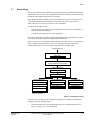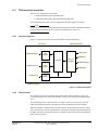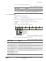
1
Cortex -M3
™
Revision r2p1
Technical Reference Manual
Copyright © 2005-2008, 2010 ARM Limited. All rights reserved.
ARM DDI 0337I (ID072410)
Cortex-M3
Technical Reference Manual
Copyright © 2005-2008, 2010 ARM Limited. All rights reserved.
Release Information
The following changes have been made to this book.
Change History
Date
Issue
Confidentiality
Change
15 December 2005
A
Confidential
First Release
13 January 2006
B
Non-Confidential
Confidentiality status amended
10 May 2006
C
Non-Confidential
First Release for r1p0
27 September 2006
D
Non-Confidential
First Release for r1p1
13 June 2007
E
Non-Confidential
Minor update with no technical changes
11 April 2008
F
Confidential
Limited release for SC300 r0p0
26 June 2008
G
Non-Confidential
First Release for r2p0
26 February 2010
H
Non-Confidential
Second Release for r2p0
07 July 2010
I
Non-Confidential
First Release for r2p1
Proprietary Notice
Words and logos marked with ® or ™ are registered trademarks or trademarks of ARM Limited in the EU and other
countries, except as otherwise stated in this proprietary notice. Other brands and names mentioned herein may be the
trademarks of their respective owners.
Neither the whole nor any part of the information contained in, or the product described in, this document may be
adapted or reproduced in any material form except with the prior written permission of the copyright holder.
The product described in this document is subject to continuous developments and improvements. All particulars of the
product and its use contained in this document are given by ARM Limited in good faith. However, all warranties implied
or expressed, including but not limited to implied warranties of merchantability, or fitness for purpose, are excluded.
This document is intended only to assist the reader in the use of the product. ARM Limited shall not be liable for any
loss or damage arising from the use of any information in this document, or any error or omission in such information,
or any incorrect use of the product.
Where the term ARM is used it means “ARM or any of its subsidiaries as appropriate”.
Confidentiality Status
This document is Non-Confidential. The right to use, copy and disclose this document may be subject to license
restrictions in accordance with the terms of the agreement entered into by ARM and the party that ARM delivered this
document to.
Product Status
The information in this document is Final (information on a developed product).
Web Address
http://www.arm.com
ARM DDI 0337I
ID072410
Copyright © 2005-2008, 2010 ARM Limited. All rights reserved.
Non-Confidential
ii
Contents
Cortex-M3 Technical Reference Manual
Preface
About this book ............................................................................................................ x
Feedback .................................................................................................................. xiii
Chapter 1
Introduction
1.1
1.2
1.3
1.4
1.5
1.6
Chapter 2
About the functions .................................................................................................. 2-2
Interfaces ................................................................................................................. 2-4
Programmers Model
3.1
3.2
3.3
3.4
3.5
3.6
3.7
3.8
3.9
ARM DDI 0337I
ID072410
1-2
1-3
1-4
1-5
1-6
1-9
Functional Description
2.1
2.2
Chapter 3
About the processor .................................................................................................
Features ...................................................................................................................
Interfaces .................................................................................................................
Configurable options ................................................................................................
Product documentation ............................................................................................
Product revisions .....................................................................................................
About the programmers model ................................................................................ 3-2
Modes of operation and execution ........................................................................... 3-3
Instruction set summary ........................................................................................... 3-4
System address map ............................................................................................. 3-11
Write buffer ............................................................................................................ 3-14
Exclusive monitor ................................................................................................... 3-15
Bit-banding ............................................................................................................. 3-16
Processor core register summary .......................................................................... 3-18
Exceptions ............................................................................................................. 3-20
Copyright © 2005-2008, 2010 ARM Limited. All rights reserved.
Non-Confidential
iii
Contents
Chapter 4
System Control
4.1
4.2
4.3
Chapter 5
About system control ............................................................................................... 4-2
Register summary .................................................................................................... 4-3
Register descriptions ............................................................................................... 4-5
Memory Protection Unit
5.1
5.2
5.3
Chapter 6
About the MPU ........................................................................................................ 5-2
MPU functional description ...................................................................................... 5-3
MPU programmers model ........................................................................................ 5-4
Nested Vectored Interrupt Controller
6.1
6.2
6.3
Chapter 7
Debug
7.1
7.2
7.3
Chapter 8
About the ETM ....................................................................................................... 10-2
ETM functional description .................................................................................... 10-3
ETM Programmers model ...................................................................................... 10-9
Trace Port Interface Unit
11.1
11.2
11.3
Appendix A
About the ITM .......................................................................................................... 9-2
ITM functional description ........................................................................................ 9-3
ITM programmers model ......................................................................................... 9-4
Embedded Trace Macrocell
10.1
10.2
10.3
Chapter 11
About the DWT ........................................................................................................ 8-2
DWT functional description ...................................................................................... 8-3
DWT Programmers Model ....................................................................................... 8-4
Instrumentation Trace Macrocell Unit
9.1
9.2
9.3
Chapter 10
About debug ............................................................................................................ 7-2
About the AHB-AP ................................................................................................... 7-6
About the Flash Patch and Breakpoint Unit (FPB) .................................................. 7-9
Data Watchpoint and Trace Unit
8.1
8.2
8.3
Chapter 9
About the NVIC ........................................................................................................ 6-2
NVIC functional description ..................................................................................... 6-3
NVIC programmers model ....................................................................................... 6-4
About the Cortex-M3 TPIU .................................................................................... 11-2
TPIU functional description .................................................................................... 11-3
TPIU programmers model ..................................................................................... 11-5
Revisions
Glossary
ARM DDI 0337I
ID072410
Copyright © 2005-2008, 2010 ARM Limited. All rights reserved.
Non-Confidential
iv
List of Tables
Cortex-M3 Technical Reference Manual
Table 1-1
Table 3-1
Table 3-2
Table 4-1
Table 4-2
Table 4-3
Table 4-4
Table 5-1
Table 6-1
Table 6-2
Table 7-1
Table 7-2
Table 7-3
Table 7-4
Table 7-5
Table 7-6
Table 7-7
Table 8-1
Table 9-1
Table 9-2
Table 10-1
Table 10-2
Table 10-3
Table 10-4
Table 10-5
Table 10-6
Table 10-7
Table 10-8
Table 10-9
ARM DDI 0337I
ID072410
Change History ............................................................................................................................... ii
Optional implementation components ......................................................................................... 1-5
Cortex-M3 instruction set summary ............................................................................................ 3-4
Memory regions ........................................................................................................................ 3-11
System control registers ............................................................................................................. 4-3
ACTLR bit assignments .............................................................................................................. 4-5
CPUID bit assignments ............................................................................................................... 4-6
AFSR bit assignments ................................................................................................................ 4-6
MPU registers ............................................................................................................................. 5-4
NVIC registers ............................................................................................................................. 6-4
ICTR bit assignments .................................................................................................................. 6-5
Cortex-M3 ROM table identification values ................................................................................. 7-3
Cortex-M3 ROM table components ............................................................................................ 7-4
SCS identification values ............................................................................................................ 7-5
Debug registers ........................................................................................................................... 7-5
AHB-AP register summary .......................................................................................................... 7-6
CSW bit assignments .................................................................................................................. 7-7
FPB register summary .............................................................................................................. 7-10
DWT register summary ............................................................................................................... 8-4
ITM register summary ................................................................................................................. 9-4
ITM_TPR bit assignments ........................................................................................................... 9-5
Cortex-M3 resources ................................................................................................................ 10-4
Boolean function encoding for events ....................................................................................... 10-5
Resource identification encoding .............................................................................................. 10-5
Input connections ...................................................................................................................... 10-7
Trigger output connections ....................................................................................................... 10-8
ETM registers ............................................................................................................................ 10-9
ETMCR bit assignments ......................................................................................................... 10-12
ETMCCR bit assignments ....................................................................................................... 10-14
ETMSCR bit assignments ....................................................................................................... 10-15
Copyright © 2005-2008, 2010 ARM Limited. All rights reserved.
Non-Confidential
v
List of Tables
Table 10-10
Table 10-11
Table 10-12
Table 10-13
Table 10-14
Table 10-15
Table 10-16
Table 10-17
Table 10-18
Table 11-1
Table 11-2
Table 11-3
Table 11-4
Table 11-5
Table 11-6
Table 11-7
Table 11-8
Table 11-9
Table 11-10
Table 11-11
Table A-1
Table A-2
Table A-3
Table A-4
ARM DDI 0337I
ID072410
ETMTECR1 bit assignments ................................................................................................... 10-16
ETMIDR bit assignments ........................................................................................................ 10-17
ETMCCER bit assignments .................................................................................................... 10-18
ETMTESSEICR bit assignments ............................................................................................ 10-19
ETMPDSR bit assignments .................................................................................................... 10-20
ITMISCIN bit assignments ...................................................................................................... 10-21
ITTRIGOUT bit assignments ................................................................................................... 10-21
ETM_ITATBCTR2 bit assignments ......................................................................................... 10-22
ETM_ITATBCTR0 bit assignments ......................................................................................... 10-22
TPIU registers ........................................................................................................................... 11-5
TPIU_ACPR bit assignments .................................................................................................... 11-6
TPIU_FFSR bit assignments .................................................................................................... 11-7
TPIU_FFCR bit assignments .................................................................................................... 11-7
TRIGGER bit assignments ........................................................................................................ 11-8
Integration ETM bit assignments .............................................................................................. 11-9
ITATBCTR2 bit assignments .................................................................................................. 11-10
Integration ITM Data bit assignments ..................................................................................... 11-10
ITATBCTR0 bit assignments .................................................................................................. 11-11
TPIU_ITCTRL bit assignments ............................................................................................... 11-12
TPIU_DEVID bit assignments ................................................................................................. 11-12
Differences between issue E and issue F ................................................................................... A-1
Differences between issue F and issue G .................................................................................. A-4
Differences between issue G and issue H .................................................................................. A-5
Differences between issue H and issue I .................................................................................... A-6
Copyright © 2005-2008, 2010 ARM Limited. All rights reserved.
Non-Confidential
vi
List of Figures
Cortex-M3 Technical Reference Manual
Figure 2-1
Figure 3-1
Figure 3-2
Figure 3-3
Figure 4-1
Figure 4-2
Figure 4-3
Figure 6-1
Figure 7-1
Figure 7-2
Figure 9-1
Figure 10-1
Figure 10-2
Figure 10-3
Figure 10-4
Figure 10-5
Figure 10-6
Figure 10-7
Figure 10-8
Figure 10-9
Figure 10-10
Figure 10-11
Figure 10-12
Figure 10-13
Figure 11-1
Figure 11-2
Figure 11-3
Figure 11-4
Figure 11-5
Figure 11-6
ARM DDI 0337I
ID072410
Cortex-M3 block diagram ............................................................................................................ 2-2
System address map ................................................................................................................ 3-11
Bit-band mapping ...................................................................................................................... 3-17
Processor register set ............................................................................................................... 3-18
ACTLR bit assignments .............................................................................................................. 4-5
CPUID bit assignments ............................................................................................................... 4-6
AFSR bit assignments ................................................................................................................ 4-6
ICTR bit assignments .................................................................................................................. 6-4
CoreSight discovery .................................................................................................................... 7-2
CSW bit assignments .................................................................................................................. 7-7
ITM_TPR bit assignments ........................................................................................................... 9-5
ETM block diagram ................................................................................................................... 10-3
ETMCR bit assignments ......................................................................................................... 10-11
ETMCCR bit assignments ....................................................................................................... 10-14
ETMSCR bit assignments ....................................................................................................... 10-15
ETMTECR1 bit assignments ................................................................................................... 10-16
ETMIDR bit assignments ........................................................................................................ 10-17
ETMCCER bit assignments .................................................................................................... 10-18
ETMTESSEICR bit assignments ............................................................................................ 10-19
ETMPDSR bit assignments .................................................................................................... 10-20
ITMISCIN bit assignments ...................................................................................................... 10-20
ITTRIGOUT bit assignments ................................................................................................... 10-21
ETM_ITATBCTR2 bit assignments ......................................................................................... 10-22
ETM_ITATBCTR0 bit assignments ......................................................................................... 10-22
TPIU block diagram .................................................................................................................. 11-3
TPIU_ACPR bit assignments .................................................................................................... 11-6
TPIU_FFSR bit assignments .................................................................................................... 11-6
TPIU_FFCR bit assignments .................................................................................................... 11-7
TRIGGER bit assignments ........................................................................................................ 11-8
Integration ETM Data bit assignments ...................................................................................... 11-9
Copyright © 2005-2008, 2010 ARM Limited. All rights reserved.
Non-Confidential
vii
List of Figures
Figure 11-7
Figure 11-8
Figure 11-9
Figure 11-10
Figure 11-11
Figure 11-12
ARM DDI 0337I
ID072410
ITATBCTR2 bit assignments .................................................................................................... 11-9
Integration ITM Data bit assignments ..................................................................................... 11-10
ITATBCTR0 bit assignments .................................................................................................. 11-11
TPIU_ITCTRL bit assignments ............................................................................................... 11-11
TPIU_DEVID bit assignments ................................................................................................. 11-12
TPIU_DEVTYPE bit assignments ........................................................................................... 11-13
Copyright © 2005-2008, 2010 ARM Limited. All rights reserved.
Non-Confidential
viii
Preface
This preface introduces the Cortex-M3 Technical Reference Manual (TRM). It contains the
following sections:
•
About this book on page x
•
Feedback on page xiii.
ARM DDI 0337I
ID072410
Copyright © 2005-2008, 2010 ARM Limited. All rights reserved.
Non-Confidential
ix
Preface
About this book
This book is for the Cortex-M3 processor.
Product revision status
The rnpn identifier indicates the revision status of the product described in this manual, where:
rn
Identifies the major revision of the product.
pn
Identifies the minor revision or modification status of the product.
Intended audience
This manual is written to help system designers, system integrators, verification engineers, and
software programmers who are implementing a System-on-Chip (SoC) device based on the
Cortex-M3 processor.
Using this book
This book is organized into the following chapters:
Chapter 1 Introduction
Read this for a description of the components of the processor, and of the product
documentation.
Chapter 2 Functional Description
Read this for a description of the functionality of the processor.
Chapter 3 Programmers Model
Read this for a description of the processor register set, modes of operation, and
other information for programming the processor.
Chapter 4 System Control
Read this for a description of the registers and programmers model for system
control.
Chapter 5 Memory Protection Unit
Read this for a description of the Memory Protection Unit (MPU).
Chapter 6 Nested Vectored Interrupt Controller
Read this for a description of the interrupt processing and control.
Chapter 7 Debug
Read this for information about debugging and testing the processor core.
Chapter 8 Data Watchpoint and Trace Unit
Read this for a description of the Data Watchpoint and Trace (DWT) unit.
Chapter 9 Instrumentation Trace Macrocell Unit
Read this for a description of the Instrumentation Trace Macrocell (ITM) unit.
Chapter 10 Embedded Trace Macrocell
Read this for a description of the processor Embedded Trace Macrocell (ETM).
Chapter 11 Trace Port Interface Unit
Read this for a description of the Trace Port Interface Unit (TPIU).
ARM DDI 0337I
ID072410
Copyright © 2005-2008, 2010 ARM Limited. All rights reserved.
Non-Confidential
x
Preface
Appendix A Revisions
Read this for a description of the technical changes between released issues of this
book.
Glossary
Read this for definitions of terms used in this book.
Conventions
Conventions that this book can use are described in:
•
Typographical
Typographical
The typographical conventions are:
italic
Highlights important notes, introduces special terminology, denotes
internal cross-references, and citations.
bold
Highlights interface elements, such as menu names. Denotes signal
names. Also used for terms in descriptive lists, where appropriate.
monospace
Denotes text that you can enter at the keyboard, such as commands, file
and program names, and source code.
monospace
Denotes a permitted abbreviation for a command or option. You can enter
the underlined text instead of the full command or option name.
monospace italic
Denotes arguments to monospace text where the argument is to be
replaced by a specific value.
monospace
Denotes language keywords when used outside example code.
< and >
Enclose replaceable terms for assembler syntax where they appear in code
or code fragments. For example:
ADD Rd, Rn, <op2>
Additional reading
This section lists publications by ARM and by third parties.
See Infocenter, http://infocenter.arm.com, for access to ARM documentation.
ARM publications
This book contains information that is specific to this product. See the following documents for
other relevant information:
•
ARMv7-M Architecture Reference Manual (ARM DDI 0403)
•
ARM Cortex-M3 Integration and Implementation Manual (ARM DII 0240)
•
ARM AMBA® 3 AHB-Lite Protocol (v1.0) (ARM IHI 0033)
•
ARM AMBA™ 3 APB Protocol Specification (ARM IHI 0024)
•
AMBA® 3 ATB Protocol Specification (ARM IHI 0032)
•
ARM CoreSight™ Components Technical Reference Manual (ARM DDI 0314)
•
ARM Debug Interface v5 Architecture Specification (ARM IHI 0031)
•
ARM Embedded Trace Macrocell Architecture Specification (ARM IHI 0014).
ARM DDI 0337I
ID072410
Copyright © 2005-2008, 2010 ARM Limited. All rights reserved.
Non-Confidential
xi
Preface
Other publications
This section lists relevant documents published by third parties:
•
IEEE Standard Test Access Port and Boundary-Scan Architecture 1149.1-2001 (JTAG).
ARM DDI 0337I
ID072410
Copyright © 2005-2008, 2010 ARM Limited. All rights reserved.
Non-Confidential
xii
Preface
Feedback
ARM welcomes feedback on this product and its documentation.
Feedback on this product
If you have any comments or suggestions about this product, contact your supplier and give:
•
The product name.
•
The product revision or version.
•
An explanation with as much information as you can provide. Include symptoms and
diagnostic procedures if appropriate.
Feedback on this manual
If you have comments on content then send e-mail to [email protected]. Give:
•
the title
•
the number, ARM DDI 0337I
•
the page number(s) to which your comments refer
•
a concise explanation of your comments.
ARM also welcomes general suggestions for additions and improvements.
ARM DDI 0337I
ID072410
Copyright © 2005-2008, 2010 ARM Limited. All rights reserved.
Non-Confidential
xiii
Chapter 1
Introduction
This chapter introduces the processor and instruction set. It contains the following sections:
•
About the processor on page 1-2
•
Features on page 1-3
•
Interfaces on page 1-4
•
Configurable options on page 1-5
•
Product documentation on page 1-6
•
Product revisions on page 1-9.
ARM DDI 0337I
ID072410
Copyright © 2005-2008, 2010 ARM Limited. All rights reserved.
Non-Confidential
1-1
Introduction
1.1
About the processor
The Cortex-M3 is a low-power processor that features low gate count, low interrupt latency, and
low-cost debug. It is intended for deeply embedded applications that require optimal interrupt
response features.
ARM DDI 0337I
ID072410
Copyright © 2005-2008, 2010 ARM Limited. All rights reserved.
Non-Confidential
1-2
Introduction
1.2
Features
The Cortex-M3 processor incorporates:
ARM DDI 0337I
ID072410
•
a processor core
•
a Nested Vectored Interrupt Controller (NVIC) closely integrated with the processor core
to achieve low latency interrupt processing
•
multiple high-performance bus interfaces
•
a low-cost debug solution with the optional ability to:
— implement breakpoints and code patches
— implement watchpoints, tracing, and system profiling
— support printf() style debugging.
— bridge to a Trace Port Analyzer (TPA).
•
an optional Memory Protection Unit (MPU).
Copyright © 2005-2008, 2010 ARM Limited. All rights reserved.
Non-Confidential
1-3
Introduction
1.3
Interfaces
The processor has the following external interfaces:
•
multiple memory and device bus interfaces
•
ETM interface
•
trace port interface
•
debug port interface
•
if the implementation includes an ETM, a Cross Trigger Interface (CTI).
ARM DDI 0337I
ID072410
Copyright © 2005-2008, 2010 ARM Limited. All rights reserved.
Non-Confidential
1-4
Introduction
1.4
Configurable options
You can configure your Cortex-M3 implementation to include the following optional
components:
Table 1-1 Optional implementation components
Component
Description
MPU
See Chapter 5 Memory Protection Unit
FPB
Flash Patch and Breakpoint Unit. See Chapter 7
Debug
DWT
See Chapter 8 Data Watchpoint and Trace Unit
ITM
See Chapter 9 Instrumentation Trace Macrocell Unit
ETM
See Chapter 10 Embedded Trace Macrocell
AHB-AP
Advanced High-performance Bus Access Port. See
Chapter 7 Debug
HTM interface
See AHB Trace Macrocell interface on page 2-6
TPIU
See Chapter 11 Trace Port Interface Unit
WIC
Wake-up Interrupt Controller. See Low power modes
on page 6-3
Debug Port
See Debug Port AHB-AP interface on page 2-6
Constant AHB control
See Bus interfaces on page 2-4
Note
You can only configure trace functionality in the following combinations:
•
no trace functionality
•
ITM and DWT
•
ITM, DWT, and ETM
•
ITM, DWT, ETM, and HTM.
You can configure the debug features provided in the DWT independently.
ARM DDI 0337I
ID072410
Copyright © 2005-2008, 2010 ARM Limited. All rights reserved.
Non-Confidential
1-5
Introduction
1.5
Product documentation
This section describes the processor books, how they relate to the design flow, and the relevant
architectural standards and protocols.
See Additional reading on page xi for more information about the books described in this
section.
1.5.1
Documentation
The Cortex-M3 documentation is as follows:
Technical Reference Manual
The Technical Reference Manual (TRM) describes the functionality and the
effects of functional options on the behavior of the Cortex-M3 processor. It is
required at all stages of the design flow. Some behavior described in the TRM
might not be relevant because of the way that the Cortex-M3 processor is
implemented and integrated. If you are programming the Cortex-M3 processor
then contact:
•
•
the implementer to determine:
—
the build configuration of the implementation
—
what integration, if any, was performed before implementing the
processor.
the integrator to determine the pin configuration of the SoC that you are
using.
Integration and Implementation Manual
The Integration and Implementation Manual (IIM) describes:
•
The available build configuration options and related issues in selecting
them.
•
How to configure the Register Transfer Level (RTL) with the build
configuration options.
•
How to integrate the processor into a SoC. This includes a description of
the integration kit and describes the pins that the integrator must tie off to
configure the macrocell for the required integration.
•
How to implement the processor into your design. This includes
floorplanning guidelines, Design for Test (DFT) information, and how to
perform netlist dynamic verification on the processor.
•
The processes to sign off the integration and implementation of the design.
The ARM product deliverables include reference scripts and information about
using them to implement your design.
Reference methodology documentation from your EDA tools vendor
complements the IIM.
The IIM is a confidential book that is only available to licensees.
Cortex-M3 User Guide Reference Material
This document provides reference material that ARM partners can configure and
include in a User Guide for an ARM Cortex-M3 processor. Typically:
•
ARM DDI 0337I
ID072410
each chapter in this reference material might correspond to a section in the
User Guide
Copyright © 2005-2008, 2010 ARM Limited. All rights reserved.
Non-Confidential
1-6
Introduction
•
each top-level section in this reference material might correspond to a
chapter in the User Guide.
However, ARM partners can organize this material in any way, subject to the
conditions of the licence agreement under which ARM supplied the material.
1.5.2
Design Flow
The processor is delivered as synthesizable RTL. Before it can be used in a product, it must go
through the following process:
Implementation
The implementer configures the RTL and may synthesize it to produce a hard
macrocell or may synthesize the whole design after implementation.
Integration The integrator connects the implemented design into a SoC. This includes
connecting it to a memory system and peripherals.
Programming
The system programmer develops the software required to configure and
initialize the processor, and tests the required application software.
Each stage in the process can be performed by a different party. Implementation and integration
choices affect the behavior and features of the processor.
For MCUs, often a single design team integrates the processor before synthesizing the complete
design. Alternatively, the team can synthesise the processor on its own or partially integrated,
to produce a macrocell that is then integrated, possibly by a separate team.
The operation of the final device depends on:
Build configuration
The implementer chooses the options that affect how the RTL source files are
pre-processed. These options usually include or exclude logic that affects one or
more of the area, maximum frequency, and features of the resulting macrocell.
Configuration inputs
The integrator configures some features of the processor by tying inputs to
specific values. These configurations affect the start-up behavior before any
software configuration is made. They can also limit the options available to the
software.
Software configuration
The programmer configures the processor by programming particular values into
registers. This affects the behavior of the processor.
Note
This manual refers to implementation-defined features that are applicable to build configuration
options. Reference to a feature that is included means that the appropriate build and pin
configuration options are selected. Reference to an enabled feature means one that has also been
configured by software.
1.5.3
Architecture and protocol information
The processor complies with, or implements, the specifications described in:
•
ARM architecture on page 1-8
ARM DDI 0337I
ID072410
Copyright © 2005-2008, 2010 ARM Limited. All rights reserved.
Non-Confidential
1-7
Introduction
•
•
•
Bus architecture
Debug
Embedded Trace Macrocell.
This book complements architecture reference manuals, architecture specifications, protocol
specifications, and relevant external standards. It does not duplicate information from these
sources.
ARM architecture
The processor implements the ARMv7-M architecture profile. See the ARMv7-M Architecture
Reference Manual.
For more information about architectural compliance, see Architecture and protocol
information on page 1-9.
Bus architecture
The processor provides three primary bus interfaces implementing a variant of the AMBA 3
AHB-Lite protocol. The processor implements an interface for CoreSight and other debug
components using the AMBA 3 APB protocol. See:
•
the ARM AMBA 3 AHB-Lite Protocol (v1.0)
•
the ARM AMBA 3 APB Protocol Specification.
Debug
The debug features of the processor implement the ARM debug interface architecture. See the
ARM Debug Interface v5 Architecture Specification. The processor also implements debug
features defined by the ARMv7-M. See the ARMv7-M Architecture Reference Manual.
Embedded Trace Macrocell
The trace features of the processor implement version 3.4 of the ARM Embedded Trace
Macrocell architecture. See the ARM Embedded Trace Macrocell Architecture Specification.
ARM DDI 0337I
ID072410
Copyright © 2005-2008, 2010 ARM Limited. All rights reserved.
Non-Confidential
1-8
Introduction
1.6
Product revisions
This section summarizes the differences in functionality between the different releases of this
processor:
•
Differences in functionality between r0p0 and r1p0
•
Differences in functionality between r1p0 and r1p1
•
Differences in functionality between r1p1 and r2p0 on page 1-10
•
Differences in functionality between r2p0 and r2p1 on page 1-10.
1.6.1
Differences in functionality between r0p0 and r1p0
In summary, the differences in functionality include:
1.6.2
•
Addition of configurable data value comparison to the DWT module.
•
Addition of a MATCHED bit to DWT_FUNCTION.
•
Addition of configurable ETMFIFOFULL stalling functionality to the processor and the
ETM.
•
Addition of SWV Mode to the ITM.
•
CPUID Base Register VARIANT field changed to indicate Rev1.
•
Cortex-M3 Rev0 Bit-band accesses in BE8 mode required access sizes to be byte.
Cortex-M3 Rev1 has been changed so that BE8 bit-band accesses function with any
access size.
•
Addition of a configuration bit called STKALIGN to ensure that all exceptions have
eight-byte stack alignment.
•
Addition of the Auxiliary Fault Status Register at address 0xE000ED3C. To set this register,
a 32-bit input bus called AUXFAULT has been added.
•
Addition of HTM support.
•
ICode and DCode cacheable and bufferable HPROT values permanently tied to
write-through.
•
Addition of the SWJ-DP. This is the standard CoreSight™ debug port that combines
JTAG-DP and SW-DP.
•
Addition of DWT_PCSR Register at address 0xE000101C.
•
Errata fixes to the r0p0 release.
Differences in functionality between r1p0 and r1p1
In summary, the differences in functionality include:
ARM DDI 0337I
ID072410
•
Data value matching for watchpoint generation has been made implementation time
configurable.
•
Architectural clock gating in the ETM is configurable at implementation.
•
DAPCLKEN was required to be a static signal in r0p0 and r1p0. This requirement has
been removed for r1p1.
•
SLEEPING signal now suppressed until current outstanding instruction fetch has
completed.
Copyright © 2005-2008, 2010 ARM Limited. All rights reserved.
Non-Confidential
1-9
Introduction
•
1.6.3
Errata fixes to the r1p0 release.
Differences in functionality between r1p1 and r2p0
In summary, the differences in functionality include:
1.6.4
•
Implementation time options have been added to select between different levels of debug
and trace support. This has replaced the previous TIEOFF_FPBEN and
TIEOFF_TRCENA options.
•
New implementation option to enable the resetting of all registers within the processor.
•
Architectural clock gating inclusion is now controlled using one implementation option.
•
DBGRESTART input and DBGRESTARTED output have been added for use in
debugging multi-core systems. See the ARMv7-M Architecture Reference Manual for
more information.
•
SLEEPHOLDREQn input and SLEEPHOLDACKn have been added to enable the
extension of SLEEPING.
•
The APB interface has been upgraded from v2.0 to v3.0.
•
A new output signal called INTERNALSTATE has been added that enables observation
of some of the internal state of the core if the OBSERVATION implementation option is
used.
•
Added support for fault-robust implementations.
•
An Auxiliary Control Register has been added with new functionality disable bits to:
—
stop interruption of load/store multiples, divides and multiplies
—
stop IT folding
—
disable the write buffers in Cortex-M3 for default memory map accesses.
•
The STKALIGN bit reset value in the Configuration and Control Register at address
0xE000ED14 has been inverted. The reset value is now 1, which means that the stack frame
is 8-byte aligned by default.
•
Addition of a Wake-up Interrupt Controller to minimize logic in the always clocked
domain during sleep.
•
Addition of FIXHMASTERTYPE pin to prevent debugger marking AHB transactions
as core data side if required.
•
Improved sequential information for data accesses. Before r2p0 HPROT for sequential
data accesses would change from SEQ to NSEQ if wait-states were inserted for the
previous access. r2p0 maintains the SEQ information.
•
Errata fixes to the r1p1 release.
Differences in functionality between r2p0 and r2p1
In summary, the differences in functionality include:
ARM DDI 0337I
ID072410
•
New implementation option to ensure constant AHB control during wait-stated transfers.
•
New implementation option to remove the bit-banding logic.
•
MPUDISABLE input added to disable the MPU via hardware.
Copyright © 2005-2008, 2010 ARM Limited. All rights reserved.
Non-Confidential
1-10
Introduction
ARM DDI 0337I
ID072410
•
DBGEN input added as master debug enable. If de-asserted then debug is disabled.
•
ETM upgraded from ARM ETM architecture v3.4 to 3.5 to include global time-stamping.
•
The Vector Table Offset Register located at address 0xE000ED08 has been increased by
two bits from 29:7 to 31:7.
•
ROM table identification registers have been updated. See Cortex-M3 ROM table
identification and entries on page 7-3.
•
Verilog file and module names have been modified. The top module names for Cortex-M3
and the integration layer are now in capitals: CORTEXM3 and
CORTEXM3INTEGRATION.
•
The ETM license define name has changed to ARM_CM3_ETM_LICENSE and is now
defined in cm3_lic_defs.v rather than in the integration level.
•
Watchpoints no longer occur if the transaction is aborted by the MPU.
•
Errata fixes to the r2p0 release.
Copyright © 2005-2008, 2010 ARM Limited. All rights reserved.
Non-Confidential
1-11
Chapter 2
Functional Description
This chapter introduces the processor and its external interfaces. It contains the following sections:
•
About the functions on page 2-2
•
Interfaces on page 2-4.
ARM DDI 0337I
ID072410
Copyright © 2005-2008, 2010 ARM Limited. All rights reserved.
Non-Confidential
2-1
Functional Description
2.1
About the functions
Figure 2-1 shows the structure of the Cortex-M3 processor.
Cortex-M3 processor
Nested
Vectored
Interrupt
Controller
(NVIC)
Interrupts and
power control
†
Cortex-M3
processor core
Embedded
Trace
Macrocell
(ETM)
†
Wake-up
Interrupt
Controller
(WIC)
† Serial-Wire
or JTAG
Debug Port
(SW-DP or
SWJ-DP)
Serial-Wire or
JTAG Debug
Interface
†
†
Flash Patch
Breakpoint
(FPB)
†
Data
Watchpoint
and Trace
(DWT)
Memory
Protection
Unit (MPU)
†
†
AHB
Access Port
(AHB-AP)
ICode
AHB-Lite
instruction
interface
Bus Matrix
DCode
AHB-Lite
data
interface
System
AHB-Lite
system
interface
†
Instrumentation
Trace Macrocell
(ITM)
Trace Port
Interface Unit
(TPIU)
Trace Port
Interface
† CoreSight
ROM table
PPB APB
debug system
interface
† Optional component
Figure 2-1 Cortex-M3 block diagram
The Cortex-M3 processor features:
•
ARM DDI 0337I
ID072410
A low gate count processor core, with low latency interrupt processing that has:
—
A subset of the Thumb instruction set, defined in the ARMv7-M Architecture
Reference Manual.
—
Banked Stack Pointer (SP).
—
Hardware integer divide instructions, SDIV and UDIV.
—
Handler and Thread modes.
—
Thumb and Debug states.
—
Support for interruptible-continued instructions LDM, STM, PUSH, and POP for low
interrupt latency.
—
Automatic processor state saving and restoration for low latency Interrupt Service
Routine (ISR) entry and exit.
—
Support for ARMv6 big-endian byte-invariant or little-endian accesses.
—
Support for ARMv6 unaligned accesses.
Copyright © 2005-2008, 2010 ARM Limited. All rights reserved.
Non-Confidential
2-2
Functional Description
•
•
•
•
ARM DDI 0337I
ID072410
Nested Vectored Interrupt Controller (NVIC) closely integrated with the processor core
to achieve low latency interrupt processing. Features include:
—
External interrupts, configurable from 1 to 240.
—
Bits of priority, configurable from 3 to 8.
—
Dynamic reprioritization of interrupts.
—
Priority grouping. This enables selection of preempting interrupt levels and non
preempting interrupt levels.
—
Support for tail-chaining and late arrival of interrupts. This enables back-to-back
interrupt processing without the overhead of state saving and restoration between
interrupts.
—
Processor state automatically saved on interrupt entry, and restored on interrupt exit,
with no instruction overhead.
—
Optional Wake-up Interrupt Controller (WIC), providing ultra-low power sleep
mode support.
Memory Protection Unit (MPU). An optional MPU for memory protection, including:
—
Eight memory regions.
—
Sub Region Disable (SRD), enabling efficient use of memory regions.
—
The ability to enable a background region that implements the default memory map
attributes.
Bus interfaces:
—
Three Advanced High-performance Bus-Lite (AHB-Lite) interfaces: ICode,
DCode, and System bus interfaces.
—
Private Peripheral Bus (PPB) based on Advanced Peripheral Bus (APB) interface.
—
Bit-band support that includes atomic bit-band write and read operations.
—
Memory access alignment.
—
Write buffer for buffering of write data.
—
Exclusive access transfers for multiprocessor systems.
Low-cost debug solution that features:
—
Debug access to all memory and registers in the system, including access to
memory mapped devices, access to internal core registers when the core is halted,
and access to debug control registers even while SYSRESETn is asserted.
—
Serial Wire Debug Port (SW-DP) or Serial Wire JTAG Debug Port (SWJ-DP) debug
access.
—
Optional Flash Patch and Breakpoint (FPB) unit for implementing breakpoints and
code patches.
—
Optional Data Watchpoint and Trace (DWT) unit for implementing watchpoints,
data tracing, and system profiling.
—
Optional Instrumentation Trace Macrocell (ITM) for support of printf() style
debugging.
—
Optional Trace Port Interface Unit (TPIU) for bridging to a Trace Port Analyzer
(TPA), including Single Wire Output (SWO) mode.
—
Optional Embedded Trace Macrocell (ETM) for instruction trace.
Copyright © 2005-2008, 2010 ARM Limited. All rights reserved.
Non-Confidential
2-3
Functional Description
2.2
Interfaces
The processor contains the following external interfaces:
•
Bus interfaces
•
ETM interface on page 2-6
•
AHB Trace Macrocell interface on page 2-6
•
Debug Port AHB-AP interface on page 2-6.
2.2.1
Bus interfaces
The processor contains three external Advanced High-performance Bus (AHB)-Lite bus
interfaces and one Advanced Peripheral Bus (APB) interface:
•
ICode memory interface
•
DCode memory interface on page 2-5
•
System interface on page 2-5
•
Private Peripheral Bus (PPB) on page 2-5.
The processor matches the AMBA 3 specification except for maintaining control information
during waited transfers. The AMBA 3 AHB-Lite Protocol states that when the slave is
requesting wait states the master must not change the transfer type, except for the following
cases:
•
On an IDLE transfer, the master can change the transfer type from IDLE to NONSEQ.
•
On a BUSY transfer with a fixed length burst, the master can change the transfer type
from BUSY to SEQ.
•
On a BUSY transfer with an undefined length burst, the master can change the transfer
type from BUSY to any other transfer type.
The processor does not match this definition because it might change the access type from SEQ
or NONSEQ to IDLE during a waited transfer. The processor might also change the address or
other control information and therefore request an access to a new location. The original address
that was retracted might not be requested again. This cancels the outstanding transfer that has
not occurred because the previous access is wait-stated and awaiting completion. This is done
so that the processor can have a lower interrupt latency and higher performance in wait-stated
systems by retracting accesses that are no longer required.
To achieve complete compliance with the AMBA 3 specification you can implement the design
with the AHB_CONST_CTRL parameter set to 1. This ensures that once transfers are issued
during a wait-stated response they are never retracted or modified and the original transfer is
honoured. The consequence of setting this parameter is that the performance of the core might
decrease for wait-stated systems as a result of the interrupt and branch latency increasing.
ICode memory interface
Instruction fetches from Code memory space, 0x00000000 to 0x1FFFFFFF, are performed over this
32-bit AHB-Lite bus.
The Debugger cannot access this interface. All fetches are word-wide. The number of
instructions fetched per word depends on the code running and the alignment of the code in
memory.
ARM DDI 0337I
ID072410
Copyright © 2005-2008, 2010 ARM Limited. All rights reserved.
Non-Confidential
2-4
Functional Description
DCode memory interface
Data and debug accesses to Code memory space, 0x00000000 to 0x1FFFFFFF, are performed over
this 32-bit AHB-Lite bus. Core data accesses have a higher priority than debug accesses on this
bus. This means that debug accesses are waited until core accesses have completed when there
are simultaneous core and debug access to this bus.
Control logic in this interface converts unaligned data and debug accesses into two or three
aligned accesses, depending on the size and alignment of the unaligned access. This stalls any
subsequent data or debug access until the unaligned access has completed.
Note
ARM strongly recommends that any external arbitration between the ICode and DCode AHB
bus interfaces ensures that DCode has a higher priority than ICode.
System interface
Instruction fetches, and data and debug accesses, to address ranges 0x20000000 to 0xDFFFFFFF and
0xE0100000 to 0xFFFFFFFF are performed over this 32-bit AHB-Lite bus.
For simultaneous accesses to this bus, the arbitration order in decreasing priority is:
•
data accesses
•
instruction and vector fetches
•
debug.
The system bus interface contains control logic to handle unaligned accesses, FPB remapped
accesses, bit-band accesses, and pipelined instruction fetches.
Private Peripheral Bus (PPB)
Data and debug accesses to external PPB space, 0xE0040000 to 0xE00FFFFF, are performed over
this 32-bit Advanced Peripheral Bus (APB) bus. The Trace Port Interface Unit (TPIU) and
vendor specific peripherals are on this bus.
Core data accesses have higher priority than debug accesses, so debug accesses are waited until
core accesses have completed when there are simultaneous core and debug access to this bus.
Only the address bits necessary to decode the External PPB space are supported on this
interface.
The External PPB (EPPB) space, 0xE0040000 up to 0xE0100000, is intended for
CoreSight-compatible debug and trace components, and has a number of irregular limitations
which make it less useful for regular system peripherals. ARM recommends that system
peripherals are placed in suitable Device type areas of the System bus address space, with use
of an AHB2APB protocol converter for APB-based devices.
Limitations of the EPPB space are:
ARM DDI 0337I
ID072410
•
it is accessible in privileged mode only
•
it is accessed in little-endian fashion irrespective of the data endianness setting of the
processor
•
accesses behave as Strongly Ordered
•
no bit-band function is available
•
unaligned accesses have Unpredictable results
Copyright © 2005-2008, 2010 ARM Limited. All rights reserved.
Non-Confidential
2-5
Functional Description
2.2.2
•
only 32-bit data accesses are supported
•
it is accessible from the Debug Port and the local processor, but not from any other
processor in the system.
ETM interface
The ETM interface enables simple connection of an ETM to the processor. It provides a channel
for instruction trace to the ETM. See the ARM Embedded Trace Macrocell Architecture
Specification.
2.2.3
AHB Trace Macrocell interface
The AHB Trace Macrocell (HTM) interface enables a simple connection of the AHB trace
macrocell to the processor. It provides a channel for the data trace to the HTM.
Your implementation must include this interface to use the HTM interface. You must set
TRCENA to 1 in the Debug Exception and Monitor Control Register (DEMCR) before you
enable the HTM port to supply trace data. See the ARMv7-M Architecture Reference Manual.
2.2.4
Debug Port AHB-AP interface
The processor contains an Advanced High-performance Bus Access Port (AHB-AP) interface
for debug accesses. An external Debug Port (DP) component accesses this interface. The
Cortex-M3 system supports three possible DP implementations:
•
The Serial Wire JTAG Debug Port (SWJ-DP). The SWJ-DP is a standard CoreSight debug
port that combines JTAG-DP and Serial Wire Debug Port (SW-DP).
•
The SW-DP. This provides a two-pin interface to the AHB-AP port.
•
No DP present. If no debug functionality is present within the processor, a DP is not
required.
The two DP implementations provide different mechanisms for debug access to the processor.
Your implementation must contain only one of these components.
Note
Your implementation might contain an alternative implementer-specific DP instead of SW-DP
or SWJ-DP. See your implementer for details.
For more detailed information on the DP components, see the CoreSight Components Technical
Reference manual.
For more information on the AHB-AP, see Chapter 7 Debug.
The DP and AP together are referred to as the Debug Access Port (DAP).
For more detailed information on the debug interface, see the ARM Debug Interface v5
Architecture Specification.
ARM DDI 0337I
ID072410
Copyright © 2005-2008, 2010 ARM Limited. All rights reserved.
Non-Confidential
2-6
Chapter 3
Programmers Model
This chapter describes the processor programmers model. It contains the following sections:
•
About the programmers model on page 3-2
•
Modes of operation and execution on page 3-3
•
Instruction set summary on page 3-4
•
System address map on page 3-11
•
Write buffer on page 3-14
•
Bit-banding on page 3-16
•
Processor core register summary on page 3-18
•
Exceptions on page 3-20.
ARM DDI 0337I
ID072410
Copyright © 2005-2008, 2010 ARM Limited. All rights reserved.
Non-Confidential
3-1
Programmers Model
3.1
About the programmers model
The ARMv7-M Architecture Reference Manual provides a complete description of the
programmers model. This chapter gives an overview of the Cortex-M3 processor programmers
model that describes the implementation-defined options. It also contains the ARMv7-M
Thumb instructions the model uses, and their cycle counts for the processor. In addition:
•
Chapter 4 summarizes the system control features of the programmers model
•
Chapter 5 summarizes the MPU features of the programmers model
•
Chapter 6 summarizes the NVIC features of the programmers model
•
Chapter 7 summarizes the Debug features of the programmers model
•
Chapter 8 summarizes the DWT features of the programmers model
•
Chapter 9 summarizes the ITM features of the programmers model
•
Chapter 10 summarizes the ETM features of the programmers model
•
Chapter 11 summarizes the TPIU features of the programmers model.
ARM DDI 0337I
ID072410
Copyright © 2005-2008, 2010 ARM Limited. All rights reserved.
Non-Confidential
3-2
Programmers Model
3.2
Modes of operation and execution
This section briefly describes the modes of operation and execution of the Cortex-M3 processor.
See the ARMv7-M Architecture Reference Manual for more information.
3.2.1
Operating modes
The processor supports two modes of operation, Thread mode and Handler mode:
3.2.2
•
The processor enters Thread mode on Reset, or as a result of an exception return.
Privileged and Unprivileged code can run in Thread mode.
•
The processor enters Handler mode as a result of an exception. All code is privileged in
Handler mode.
Operating states
The processor can operate in one of two operating states:
3.2.3
•
Thumb state. This is normal execution running 16-bit and 32-bit halfword aligned Thumb
instructions.
•
Debug State. This is the state when the processor is in halting debug.
Privileged access and user access
Code can execute as privileged or unprivileged. Unprivileged execution limits or excludes
access to some resources. Privileged execution has access to all resources. Handler mode is
always privileged. Thread mode can be privileged or unprivileged.
ARM DDI 0337I
ID072410
Copyright © 2005-2008, 2010 ARM Limited. All rights reserved.
Non-Confidential
3-3
Programmers Model
3.3
Instruction set summary
This section provides information on:
•
Cortex-M3 instructions
•
Load/store timings on page 3-8
•
Binary compatibility with other Cortex processors on page 3-9.
3.3.1
Cortex-M3 instructions
The processor implements the ARMv7-M Thumb instruction set. Table 3-1 shows the
Cortex-M3 instructions and their cycle counts. The cycle counts are based on a system with zero
wait states.
Within the assembler syntax, depending on the operation, the <op2> field can be replaced with
one of the following options:
•
a simple register specifier, for example Rm
•
an immediate shifted register, for example Rm, LSL #4
•
a register shifted register, for example Rm, LSL Rs
•
an immediate value, for example #0xE000E000.
For brevity, not all load and store addressing modes are shown. See the ARMv7-M Architecture
Reference Manual for more information.
Table 3-1 uses the following abbreviations in the Cycles column:
P
The number of cycles required for a pipeline refill. This ranges from 1 to 3
depending on the alignment and width of the target instruction, and whether the
processor manages to speculate the address early.
B
The number of cycles required to perform the barrier operation. For DSB and DMB,
the minimum number of cycles is zero. For ISB, the minimum number of cycles
is equivalent to the number required for a pipeline refill.
N
The number of registers in the register list to be loaded or stored, including PC or
LR.
W
The number of cycles spent waiting for an appropriate event.
Table 3-1 Cortex-M3 instruction set summary
Operation
Description
Assembler
Cycles
Move
Register
MOV Rd, <op2>
1
16-bit immediate
MOVW Rd, #<imm>
1
Immediate into top
MOVT Rd, #<imm>
1
To PC
MOV PC, Rm
1+P
Add
ADD Rd, Rn, <op2>
1
Add to PC
ADD PC, PC, Rm
1+P
Add with carry
ADC Rd, Rn, <op2>
1
Form address
ADR Rd, <label>
1
Add
ARM DDI 0337I
ID072410
Copyright © 2005-2008, 2010 ARM Limited. All rights reserved.
Non-Confidential
3-4
Programmers Model
Table 3-1 Cortex-M3 instruction set summary (continued)
Operation
Description
Assembler
Cycles
Subtract
Subtract
SUB Rd, Rn, <op2>
1
Subtract with borrow
SBC Rd, Rn, <op2>
1
Reverse
RSB Rd, Rn, <op2>
1
Multiply
MUL Rd, Rn, Rm
1
Multiply accumulate
MLA Rd, Rn, Rm
2
Multiply subtract
MLS Rd, Rn, Rm
2
Long signed
SMULL RdLo, RdHi, Rn, Rm
3 to 5a
Long unsigned
UMULL RdLo, RdHi, Rn, Rm
3 to 5a
Long signed accumulate
SMLAL RdLo, RdHi, Rn, Rm
4 to 7a
Long unsigned accumulate
UMLAL RdLo, RdHi, Rn, Rm
4 to 7a
Signed
SDIV Rd, Rn, Rm
2 to 12b
Unsigned
UDIV Rd, Rn, Rm
2 to 12b
Signed
SSAT Rd, #<imm>, <op2>
1
Unsigned
USAT Rd, #<imm>, <op2>
1
Compare
CMP Rn, <op2>
1
Negative
CMN Rn, <op2>
1
AND
AND Rd, Rn, <op2>
1
Exclusive OR
EOR Rd, Rn, <op2>
1
OR
ORR Rd, Rn, <op2>
1
OR NOT
ORN Rd, Rn, <op2>
1
Bit clear
BIC Rd, Rn, <op2>
1
Move NOT
MVN Rd, <op2>
1
AND test
TST Rn, <op2>
1
Exclusive OR test
TEQ Rn, <op1>
Logical shift left
LSL Rd, Rn, #<imm>
1
Logical shift left
LSL Rd, Rn, Rs
1
Logical shift right
LSR Rd, Rn, #<imm>
1
Logical shift right
LSR Rd, Rn, Rs
1
Arithmetic shift right
ASR Rd, Rn, #<imm>
1
Arithmetic shift right
ASR Rd, Rn, Rs
1
Multiply
Divide
Saturate
Compare
Logical
Shift
ARM DDI 0337I
ID072410
Copyright © 2005-2008, 2010 ARM Limited. All rights reserved.
Non-Confidential
3-5
Programmers Model
Table 3-1 Cortex-M3 instruction set summary (continued)
Operation
Description
Assembler
Cycles
Rotate
Rotate right
ROR Rd, Rn, #<imm>
1
Rotate right
ROR Rd, Rn, Rs
1
With extension
RRX Rd, Rn
1
Count
Leading zeroes
CLZ Rd, Rn
1
Load
Word
LDR Rd, [Rn, <op2>]
2c
To PC
LDR PC, [Rn, <op2>]
2c + P
Halfword
LDRH Rd, [Rn, <op2>]
2c
Byte
LDRB Rd, [Rn, <op2>]
2c
Signed halfword
LDRSH Rd, [Rn, <op2>]
2c
Signed byte
LDRSB Rd, [Rn, <op2>]
2c
User word
LDRT Rd, [Rn, #<imm>]
2c
User halfword
LDRHT Rd, [Rn, #<imm>]
2c
User byte
LDRBT Rd, [Rn, #<imm>]
2c
User signed halfword
LDRSHT Rd, [Rn, #<imm>]
2c
User signed byte
LDRSBT Rd, [Rn, #<imm>]
2c
PC relative
LDR Rd,[PC, #<imm>]
2c
Doubleword
LDRD Rd, Rd, [Rn, #<imm>]
1+N
Multiple
LDM Rn, {<reglist>}
1+N
Multiple including PC
LDM Rn, {<reglist>, PC}
1+N+P
Word
STR Rd, [Rn, <op2>]
2c
Halfword
STRH Rd, [Rn, <op2>]
2c
Byte
STRB Rd, [Rn, <op2>]
2c
Signed halfword
STRSH Rd, [Rn, <op2>]
2c
Signed byte
STRSB Rd, [Rn, <op2>]
2c
User word
STRT Rd, [Rn, #<imm>]
2c
User halfword
STRHT Rd, [Rn, #<imm>]
2c
User byte
STRBT Rd, [Rn, #<imm>]
2c
User signed halfword
STRSHT Rd, [Rn, #<imm>]
2c
User signed byte
STRSBT Rd, [Rn, #<imm>]
2c
Doubleword
STRD Rd, Rd, [Rn, #<imm>]
1+N
Multiple
STM Rn, {<reglist>}
1+N
Store
ARM DDI 0337I
ID072410
Copyright © 2005-2008, 2010 ARM Limited. All rights reserved.
Non-Confidential
3-6
Programmers Model
Table 3-1 Cortex-M3 instruction set summary (continued)
Operation
Description
Assembler
Cycles
Push
Push
PUSH {<reglist>}
1+N
Push with link register
PUSH {<reglist>, LR}
1+N
Pop
POP {<reglist>}
1+N
Pop and return
POP {<reglist>, PC}
1+N+P
Load exclusive
LDREX Rd, [Rn, #<imm>]
2
Load exclusive half
LDREXH Rd, [Rn]
2
Load exclusive byte
LDREXB Rd, [Rn]
2
Store exclusive
STREX Rd, Rt, [Rn, #<imm>]
2
Store exclusive half
STREXH Rd, Rt, [Rn]
2
Store exclusive byte
STREXB Rd, Rt, [Rn]
2
Clear exclusive monitor
CLREX
1
Conditional
B<cc> <label>
1 or 1 + Pd
Unconditional
B <label>
1+P
With link
BL <label>
1+P
With exchange
BX Rm
1+P
With link and exchange
BLX Rm
1+P
Branch if zero
CBZ Rn, <label>
1 or 1 + Pd
Branch if non-zero
CBNZ Rn, <label>
1 or 1 + Pd
Byte table branch
TBB [Rn, Rm]
2+P
Halfword table branch
TBH [Rn, Rm, LSL#1]
2+P
Supervisor call
SVC #<imm>
-
If-then-else
IT... <cond>
1e
Disable interrupts
CPSID <flags>
1 or 2
Enable interrupts
CPSIE <flags>
1 or 2
Read special register
MRS Rd, <specreg>
1 or 2
Write special register
MSR <specreg>, Rn
1 or 2
Breakpoint
BKPT #<imm>
-
Signed halfword to word
SXTH Rd, <op2>
1
Signed byte to word
SXTB Rd, <op2>
1
Unsigned halfword
UXTH Rd, <op2>
1
Unsigned byte
UXTB Rd, <op2>
1
Pop
Semaphore
Branch
State change
Extend
ARM DDI 0337I
ID072410
Copyright © 2005-2008, 2010 ARM Limited. All rights reserved.
Non-Confidential
3-7
Programmers Model
Table 3-1 Cortex-M3 instruction set summary (continued)
Operation
Description
Assembler
Cycles
Bit field
Extract unsigned
UBFX Rd, Rn, #<imm>, #<imm>
1
Extract signed
SBFX Rd, Rn, #<imm>, #<imm>
1
Clear
BFC Rd, Rn, #<imm>, #<imm>
1
Insert
BFI Rd, Rn, #<imm>, #<imm>
1
Bytes in word
REV Rd, Rm
1
Bytes in both halfwords
REV16 Rd, Rm
1
Signed bottom halfword
REVSH Rd, Rm
1
Bits in word
RBIT Rd, Rm
1
Send event
SEV
1
Wait for event
WFE
1+W
Wait for interrupt
WFI
1+W
No operation
NOP
1
Instruction synchronization
ISB
1+B
Data memory
DMB
1+B
Data synchronization
DSB <flags>
1+B
Reverse
Hint
Barriers
a. UMULL, SMULL, UMLAL, and SMLAL instructions use early termination depending on the size of
the source values. These are interruptible, that is abandoned and restarted, with worst case
latency of one cycle.
b. Division operations use early termination to minimize the number of cycles required based
on the number of leading ones and zeroes in the input operands.
c. Neighboring load and store single instructions can pipeline their address and data phases.
This enables these instructions to complete in a single execution cycle.
d. Conditional branch completes in a single cycle if the branch is not taken.
e. An IT instruction can be folded onto a preceding 16-bit Thumb instruction, enabling
execution in zero cycles.
3.3.2
Load/store timings
This section describes how best to pair instructions to achieve more reductions in timing.
•
STR Rx,[Ry,#imm] is always one cycle. This is because the address generation is performed
in the initial cycle, and the data store is performed at the same time as the next instruction
is executing. If the store is to the write buffer, and the write buffer is full or not enabled,
the next instruction is delayed until the store can complete. If the store is not to the write
buffer, for example to the Code segment, and that transaction stalls, the impact on timing
is only felt if another load or store operation is executed before completion.
•
Any load with a base update is not normally pipelined. That is, base update load is
generally at least a two-cycle operation (more if stalled). However, if the next instruction
does not require to read from a register, the load is reduced to one cycle. Non register
writing instructions include CMP, TST, NOP, and non-taken IT controlled instructions.
•
LDR PC,[any] is always a blocking operation. This means at least two cycles for the load,
and three cycles for the pipeline reload. So this operation takes at least five cycles, or more
if stalled on the load or the fetch.
ARM DDI 0337I
ID072410
Copyright © 2005-2008, 2010 ARM Limited. All rights reserved.
Non-Confidential
3-8
Programmers Model
•
Any load or store that generates an address dependent on the result of a proceeding data
processing operation will stall the pipeline for an additional cycle whilst the register bank
is updated. There is no forwarding path for this scenario.
•
LDR Rx,[PC,#imm] might add a cycle because of contention with the fetch unit.
•
TBB and TBH are also blocking operations. These are at least two cycles for the load, one
cycle for the add, and three cycles for the pipeline reload. This means at least six cycles,
or more if stalled on the load or the fetch.
•
LDR [any] are pipelined when possible. This means that if the next instruction is an LDR or
STR, and the destination of the first LDR is not used to compute the address for the next
instruction, then one cycle is removed from the cost of the next instruction. So, an LDR
might be followed by an STR, so that the STR writes out what the LDR loaded. More multiple
LDRs can be pipelined together. Some optimized examples are:
—
LDR R0,[R1]; LDR R1,[R2] - normally three cycles total
—
LDR R0,[R1,R2]; STR R0,[R3,#20] - normally three cycles total
—
LDR R0,[R1,R2]; STR R1,[R3,R2] - normally three cycles total
—
LDR R0,[R1,R5]; LDR R1,[R2]; LDR R2,[R3,#4] - normally four cycles total.
•
Other instructions cannot be pipelined after STR with register offset. STR can only be
pipelined when it follows an LDR, but nothing can be pipelined after the store. Even a
stalled STR normally only takes two cycles, because of the write buffer.
•
LDREX and STREX can be pipelined exactly as LDR. Because STREX is treated more like an LDR,
it can be pipelined as explained for LDR. Equally LDREX is treated exactly as an LDR and so
can be pipelined.
•
LDRD and STRD cannot be pipelined with preceding or following instructions. However, the
two words are pipelined together. So, this operation requires three cycles when not stalled.
•
LDM and STM cannot be pipelined with preceding or following instructions. However, all
elements after the first are pipelined together. So, a three element LDM takes 2+1+1 or 5
cycles when not stalled. Similarly, an eight element store takes nine cycles when not
stalled. When interrupted, LDM and STM instructions continue from where they left off when
returned to. The continue operation adds one or two cycles to the first element when
started.
•
3.3.3
Unaligned word or halfword loads or stores add penalty cycles. A byte aligned halfword
load or store adds one extra cycle to perform the operation as two bytes. A halfword
aligned word load or store adds one extra cycle to perform the operation as two halfwords.
A byte-aligned word load or store adds two extra cycles to perform the operation as a byte,
a halfword, and a byte. These numbers increase if the memory stalls. A STR or STRH cannot
delay the processor because of the write buffer.
Binary compatibility with other Cortex processors
The processor implements a binary compatible subset of the instruction set and features
provided by other Cortex-M profile processors. You can move software, including system level
software, from the Cortex-M3 processor to other Cortex-M profile processors.
To ensure a smooth transition, ARM recommends that code designed to operate on other
Cortex-M profile processor architectures obey the following rules and configure the
Configuration and Control Register (CCR) appropriately:
ARM DDI 0337I
ID072410
•
use word transfers only to access registers in the NVIC and System Control Space (SCS).
•
treat all unused SCS registers and register fields on the processor as Do-Not-Modify.
Copyright © 2005-2008, 2010 ARM Limited. All rights reserved.
Non-Confidential
3-9
Programmers Model
•
ARM DDI 0337I
ID072410
configure the following fields in the CCR:
— STKALIGN bit to 1
— UNALIGN_TRP bit to 1
— Leave all other bits in the CCR register as their original value.
Copyright © 2005-2008, 2010 ARM Limited. All rights reserved.
Non-Confidential
3-10
Programmers Model
3.4
System address map
The processor contains a bus matrix that arbitrates the processor core and optional Debug
Access Port (DAP) memory accesses to both the external memory system and to the internal
System Control Space (SCS) and debug components.
Priority is always given to the processor to ensure that any debug accesses are as non-intrusive
as possible. For a zero wait state system, all debug accesses to system memory, SCS, and debug
resources are completely non-intrusive.
Figure 3-1 shows the system address map.
0xE0100000
0xE00FF000
0xE0042000
0xE0041000
0xE0040000
ROM Table
External PPB
ETM
TPIU
0xFFFFFFFF
System
0xE0100000
Private peripheral bus - External
0xE0040000
Private peripheral bus - Internal
0xE0040000
0xE000F000
0xE000E000
0xE0003000
0xE0002000
0xE0001000
0xE0000000
Reserved
SCS
Reserved
FPB
DWT
ITM
0x44000000
0xE0000000
External device 1.0GB
0xA0000000
External RAM
32MB
1.0GB
Bit band alias
0x60000000
0x42000000
31MB
0x40100000
1MB
0x40000000
0x24000000
32MB
Peripheral
0.5GB
Bit band region
0x40000000
SRAM
Bit band alias
0.5GB
0x20000000
0x22000000
31MB
0x20100000
1MB
0x20000000
Code
0.5GB
Bit band region
0x00000000
Figure 3-1 System address map
Table 3-2 shows the processor interfaces that are addressed by the different memory map
regions.
Table 3-2 Memory regions
Memory Map
Region
Code
Instruction fetches are performed over the ICode bus. Data accesses are performed over the DCode bus.
SRAM
Instruction fetches and data accesses are performed over the system bus.
SRAM bit-band
Alias region. Data accesses are aliases. Instruction accesses are not aliases.
Peripheral
Instruction fetches and data accesses are performed over the system bus.
ARM DDI 0337I
ID072410
Copyright © 2005-2008, 2010 ARM Limited. All rights reserved.
Non-Confidential
3-11
Programmers Model
Table 3-2 Memory regions (continued)
Memory Map
Region
Peripheral bit-band
Alias region. Data accesses are aliases. Instruction accesses are not aliases.
External RAM
Instruction fetches and data accesses are performed over the system bus.
External Device
Instruction fetches and data accesses are performed over the system bus.
Private Peripheral Bus
External and internal Private Peripheral Bus (PPB) interfaces. See Private peripheral bus.
This memory region is Execute Never (XN), and so instruction fetches are prohibited. An MPU, if present,
cannot change this.
System
System segment for vendor system peripherals. This memory region is XN, and so instruction fetches are
prohibited. An MPU, if present, cannot change this.
See the ARMv7-M Architecture Reference Manual for more information about the memory
model.
3.4.1
Private peripheral bus
The internal Private Peripheral Bus (PPB) interface provides access to:
•
the Instrumentation Trace Macrocell (ITM)
•
the Data Watchpoint and Trace (DWT)
•
the Flashpatch and Breakpoint (FPB)
•
the System Control Space (SCS), including the MPU and the NVIC.
The external PPB interface provides access to:
•
the TPIU
•
the ETM
•
the ROM table
•
implementation-specific areas of the PPB memory map.
3.4.2
Unaligned accesses that cross regions
The Cortex-M3 processor supports ARMv7 unaligned accesses, and performs all accesses as
single, unaligned accesses. They are converted into two or more aligned accesses by the DCode
and System bus interfaces.
Note
All Cortex-M3 external accesses are aligned.
Unaligned support is only available for load/store singles (LDR, LDRH, STR, STRH). Load/store
double already supports word aligned accesses, but does not permit other unaligned accesses,
and generates a fault if this is attempted.
Unaligned accesses that cross memory map boundaries are architecturally Unpredictable. The
processor behavior is boundary dependent, as follows:
•
ARM DDI 0337I
ID072410
DCode accesses wrap within the region. For example, an unaligned halfword access to the
last byte of Code space (0x1FFFFFFF) is converted by the DCode interface into a byte
access to 0x1FFFFFFF followed by a byte access to 0x00000000.
Copyright © 2005-2008, 2010 ARM Limited. All rights reserved.
Non-Confidential
3-12
Programmers Model
•
System accesses that cross into PPB space do not wrap within System space. For example,
an unaligned halfword access to the last byte of System space (0xDFFFFFFF) is converted
by the System interface into a byte access to 0xDFFFFFFF followed by a byte access to
0xE0000000. 0xE0000000 is not a valid address on the System bus.
•
System accesses that cross into Code space do not wrap within System space. For
example, an unaligned halfword access to the last byte of System space (0xFFFFFFFF) is
converted by the System interface into a byte access to 0xFFFFFFFF followed by a byte
access to 0x00000000. 0x00000000 is not a valid address on the System bus.
•
Unaligned accesses are not supported to PPB space, and so there are no boundary crossing
cases for PPB accesses.
Unaligned accesses that cross into the bit-band alias regions are also architecturally
Unpredictable. The processor performs the access to the bit-band alias address, but this does not
result in a bit-band operation. For example, an unaligned halfword access to 0x21FFFFFF is
performed as a byte access to 0x21FFFFFF followed by a byte access to 0x22000000 (the first byte
of the bit-band alias).
Unaligned loads that match against a literal comparator in the FPB are not remapped. FPB only
remaps aligned addresses.
ARM DDI 0337I
ID072410
Copyright © 2005-2008, 2010 ARM Limited. All rights reserved.
Non-Confidential
3-13
Programmers Model
3.5
Write buffer
To prevent bus wait cycles from stalling the processor during data stores, buffered stores to the
DCode and System buses go through a one-entry write buffer. If the write buffer is full,
subsequent accesses to the bus stall until the write buffer has drained. The write buffer is only
used if the bus waits the data phase of the buffered store, otherwise the transaction completes
on the bus.
DMB and DSB instructions wait for the write buffer to drain before completing. If an interrupt
comes in while DMB or DSB is waiting for the write buffer to drain, the processor returns to the
instruction following the DMB or DSB after the interrupt completes. This is because interrupt
processing acts as a memory barrier operation.
ARM DDI 0337I
ID072410
Copyright © 2005-2008, 2010 ARM Limited. All rights reserved.
Non-Confidential
3-14
Programmers Model
3.6
Exclusive monitor
The Cortex-M3 processor implements a local exclusive monitor. For more information about
semaphores and the local exclusive monitor, see the ARMv7M ARM Architecture Reference
Manual.
The local monitor within the processor has been constructed so that it does not hold any physical
address, but instead treats any access as matching the address of the previous LDREX. This
means that the implemented exclusives reservation granule is the entire memory address range.
The Cortex-M3 processor does not support exclusive accesses to bit-band regions.
ARM DDI 0337I
ID072410
Copyright © 2005-2008, 2010 ARM Limited. All rights reserved.
Non-Confidential
3-15
Programmers Model
3.7
Bit-banding
Bit-banding maps a complete word of memory onto a single bit in the bit-band region. For
example, writing to one of the alias words sets or clears the corresponding bit in the bit-band
region. This enables every individual bit in the bit-banding region to be directly accessible from
a word-aligned address using a single LDR instruction. It also enables individual bits to be toggled
without performing a read-modify-write sequence of instructions.
The processor memory map includes two bit-band regions. These occupy the lowest 1MB of the
SRAM and Peripheral memory regions respectively. These bit-band regions map each word in
an alias region of memory to a bit in a bit-band region of memory.
The System bus interface contains logic that controls bit-band accesses as follows:
•
It remaps bit-band alias addresses to the bit-band region.
•
For reads, it extracts the requested bit from the read byte, and returns this in the Least
Significant Bit (LSB) of the read data returned to the core.
•
For writes, it converts the write to an atomic read-modify-write operation.
•
The processor does not stall during bit-band operations unless it attempts to access the
System bus while the bit-band operation is being carried out.
The memory map has two 32-MB alias regions that map to two 1-MB bit-band regions:
•
Accesses to the 32-MB SRAM alias region map to the 1-MB SRAM bit-band region.
•
Accesses to the 32-MB peripheral alias region map to the 1-MB peripheral bit-band
region.
A mapping formula shows how to reference each word in the alias region to a corresponding bit,
or target bit, in the bit-band region. The mapping formula is:
bit_word_offset = (byte_offset x 32) + (bit_number × 4)
bit_word_addr = bit_band_base + bit_word_offset
where:
•
bit_word_offset is the position of the target bit in the bit-band memory region.
•
bit_word_addr is the address of the word in the alias memory region that maps to the
targeted bit.
•
bit_band_base is the starting address of the alias region.
•
byte_offset is the number of the byte in the bit-band region that contains the targeted bit.
•
bit_number is the bit position, 0 to 7, of the targeted bit.
Figure 3-2 on page 3-17 shows examples of bit-band mapping between the SRAM bit-band
alias region and the SRAM bit-band region:
ARM DDI 0337I
ID072410
•
The alias word at 0x23FFFFE0 maps to bit [0] of the bit-band byte at 0x200FFFFF: 0x23FFFFE0
= 0x22000000 + (0xFFFFF*32) + 0*4.
•
The alias word at 0x23FFFFFC maps to bit [7] of the bit-band byte at 0x200FFFFF: 0x23FFFFFC
= 0x22000000 + (0xFFFFF*32) + 7*4.
•
The alias word at 0x22000000 maps to bit [0] of the bit-band byte at 0x20000000: 0x22000000
= 0x22000000 + (0*32) + 0*4.
Copyright © 2005-2008, 2010 ARM Limited. All rights reserved.
Non-Confidential
3-16
Programmers Model
•
The alias word at 0x2200001C maps to bit [7] of the bit-band byte at 0x20000000: 0x2200001C
= 0x22000000 + (0*32) + 7*4.
32MB alias region
0x23FFFFFC
0x23FFFFF8
0x23FFFFF4
0x23FFFFF0
0x23FFFFEC
0x23FFFFE8
0x23FFFFE4
0x23FFFFE0
0x2200001C
0x22000018
0x22000014
0x22000010
0x2200000C
0x22000008
0x22000004
0x22000000
1MB SRAM bit-band region
7
6
5
4
3
2
1
0
7
6
0x200FFFFF
7
6
5
4
3
2
5
4
3
2
1
0
7
6
0x200FFFFE
1
0
7
0x20000003
6
5
4
3
2
0x20000002
5
4
3
2
1
0
7
6
0x200FFFFD
1
0
7
6
5
4
3
2
0x20000001
5
4
3
2
1
0
1
0
0x200FFFFC
1
0
7
6
5
4
3
2
0x20000000
Figure 3-2 Bit-band mapping
3.7.1
Directly accessing an alias region
Writing to a word in the alias region has the same effect as a read-modify-write operation on the
targeted bit in the bit-band region.
Bit [0] of the value written to a word in the alias region determines the value written to the
targeted bit in the bit-band region. Writing a value with bit [0] set writes a 1 to the bit-band bit,
and writing a value with bit [0] cleared writes a 0 to the bit-band bit.
Bits [31:1] of the alias word have no effect on the bit-band bit. Writing 0x01 has the same effect
as writing 0xFF. Writing 0x00 has the same effect as writing 0x0E.
Reading a word in the alias region returns either 0x01 or 0x00. A value of 0x01 indicates that the
targeted bit in the bit-band region is set. A value of 0x00 indicates that the targeted bit is clear.
Bits [31:1] are zero.
3.7.2
Directly accessing a bit-band region
You can directly access the bit-band region with normal reads and writes to that region.
ARM DDI 0337I
ID072410
Copyright © 2005-2008, 2010 ARM Limited. All rights reserved.
Non-Confidential
3-17
Programmers Model
3.8
Processor core register summary
The processor has the following 32-bit registers:
•
13 general-purpose registers, R0-R12
•
Stack Pointer (SP), R13 alias of banked registers, SP_process and SP_main
•
Link Register (LR), R14
•
Program Counter (PC), R15
•
Special-purpose Program Status Registers, (xPSR).
Figure 3-3 shows the processor register set.
low registers
high registers
Program Status Register
R0
R1
R2
R3
R4
R5
R6
R7
R8
R9
R10
R11
R12
R13 (SP)
R14 (LR)
R15 (PC)
xPSR
SP_process
SP_main
Figure 3-3 Processor register set
The general-purpose registers R0-R12 have no special architecturally-defined uses. Most
instructions that can specify a general-purpose register can specify R0-R12.
Low registers
Registers R0-R7 are accessible by all instructions that specify a
general-purpose register.
High registers
Registers R8-R12 are accessible by all 32-bit instructions that specify a
general-purpose register.
Registers R8-R12 are not accessible by any 16-bit instructions.
Registers R13, R14, and R15 have the following special functions:
Stack pointer
Register R13 is used as the Stack Pointer (SP). Because the SP ignores
writes to bits [1:0], it is autoaligned to a word, four-byte boundary.
Handler mode always uses SP_main, but you can configure Thread mode
to use either SP_main or SP_process.
Link register
Register R14 is the subroutine Link Register (LR).
The LR receives the return address from PC when a Branch and Link (BL)
or Branch and Link with Exchange (BLX) instruction is executed.
The LR is also used for exception return.
At all other times, you can treat R14 as a general-purpose register.
Program counter
ARM DDI 0337I
ID072410
Register R15 is the Program Counter (PC).
Copyright © 2005-2008, 2010 ARM Limited. All rights reserved.
Non-Confidential
3-18
Programmers Model
Bit [0] is always 0, so instructions are always aligned to word or halfword
boundaries.
See the ARMv7-M Architecture Reference Manual for more information.
ARM DDI 0337I
ID072410
Copyright © 2005-2008, 2010 ARM Limited. All rights reserved.
Non-Confidential
3-19
Programmers Model
3.9
Exceptions
The processor and the Nested Vectored Interrupt Controller (NVIC) prioritize and handle all
exceptions. When handling exceptions:
•
All exceptions are handled in Handler mode.
•
Processor state is automatically stored to the stack on an exception, and automatically
restored from the stack at the end of the Interrupt Service Routine (ISR).
•
The vector is fetched in parallel to the state saving, enabling efficient interrupt entry.
The processor supports tail-chaining that enables back-to-back interrupts without the overhead
of state saving and restoration.
You configure the number of interrupts, and bits of interrupt priority, during implementation.
Software can choose only to enable a subset of the configured number of interrupts, and can
choose how many bits of the configured priorities to use.
Note
Vector table entries are compatible with interworking between ARM and Thumb instructions.
This causes bit [0] of the vector value to load into the Execution Program Status Register
(EPSR) T-bit on exception entry. All populated vectors in the vector table entries must have bit
[0] set. Creating a table entry with bit [0] clear generates an INVSTATE fault on the first
instruction of the handler corresponding to this vector.
3.9.1
Exception handling
The processor implements advanced exception and interrupt handling, as described in the
ARMv7-M Architecture Reference Manual.
To reduce interrupt latency, the processor implements both interrupt late-arrival and interrupt
tail-chaining mechanisms, as defined by the ARMv7-M architecture:
•
There is a maximum of a twelve cycle latency from asserting the interrupt to execution of
the first instruction of the ISR when the memory being accessed has no wait states being
applied. The first instruction to be executed is fetched in parallel to the stack push.
•
Returns from interrupts similarly take twelve cycles where the instruction being returned
to is fetched in parallel to the stack pop.
•
Tail chaining requires six cycles when using zero wait state memory. No stack pushes or
pops are performed and only the instruction for the next ISR is fetched.
The processor exception model has the following implementation-defined behavior in addition
to the architecturally defined behavior:
•
exceptions on stacking from HardFault to NMI lockup at NMI priority
•
exceptions on unstacking from NMI to HardFault lockup at HardFault priority.
To minimize interrupt latency, the processor abandons any divide instruction to take any
pending interrupt. On return from the interrupt handler, the processor restarts the divide
instruction from the beginning The processor implements the Interruptible-continuable
Instruction field. Load multiple (LDM) operations and store multiple (STM) operations are
interruptible. The EPSR holds the information required to continue the load or store multiple
from the point where the interrupt occurred.
ARM DDI 0337I
ID072410
Copyright © 2005-2008, 2010 ARM Limited. All rights reserved.
Non-Confidential
3-20
Programmers Model
This means that software must not use load-multiple or store-multiple instructions to access a
device or access a memory region that is read-sensitive or sensitive to repeated writes. The
software must not use these instructions in any case where repeated reads or writes might cause
inconsistent results or unwanted side-effects.
Base register update in LDM and STM operations
There are cases when an LDM or STM updates the base register:
•
When the instruction specifies base register write-back, the base register changes to the
updated address. An abort restores the original base value.
•
When the base register is in the register list of an LDM, and is not the last register in the list,
the base register changes to the loaded value.
An LDM or STM is restarted rather than continued if:
•
the instruction faults
•
the instruction is inside an IT.
If an LDM has completed a base load, it is continued from before the base load.
ARM DDI 0337I
ID072410
Copyright © 2005-2008, 2010 ARM Limited. All rights reserved.
Non-Confidential
3-21
Chapter 4
System Control
This chapter describes the registers that program the processor. It contains the following sections:
•
About system control on page 4-2
•
Register summary on page 4-3
•
Register descriptions on page 4-5.
ARM DDI 0337I
ID072410
Copyright © 2005-2008, 2010 ARM Limited. All rights reserved.
Non-Confidential
4-1
System Control
4.1
About system control
This chapter describes the registers that control the operation of the processor.
ARM DDI 0337I
ID072410
Copyright © 2005-2008, 2010 ARM Limited. All rights reserved.
Non-Confidential
4-2
System Control
4.2
Register summary
Table 4-1 shows the system control registers. Registers not described in this chapter are
described in the ARMv7-M Architecture Reference Manual
Table 4-1 System control registers
Address
Name
Type
Reset
Description
0xE000E008
ACTLR
RW
0x00000000
Auxiliary Control Register, ACTLR on page 4-5
0xE000E010
STCSR
RW
0x00000000
SysTick Control and Status Register
0xE000E014
STRVR
RW
Unknown
SysTick Reload Value Register
0xE000E018
STCVR
RW clear
Unknown
SysTick Current Value Register
0xE000E01C
STCR
RO
Implementation specific
SysTick Calibration Value Register
0xE000ED00
CPUID
RO
0x412FC231
CPUID Base Register, CPUID on page 4-5
0xE000ED04
ICSR
RW or RO
0x00000000
Interrupt Control and State Register
0xE000ED08
VTOR
RW
0x00000000
Vector Table Offset Register
0xE000ED0C
AIRCR
RW
0x00000000a
Application Interrupt and Reset Control Register
0xE000ED10
SCR
RW
0x00000000
System Control Register
0xE000ED14
CCR
RW
0x00000200
Configuration and Control Register.
0xE000ED18
SHPR1
RW
0x00000000
System Handler Priority Register 1
0xE000ED1C
SHPR2
RW
0x00000000
System Handler Priority Register 2
0xE000ED20
SHPR3
RW
0x00000000
System Handler Priority Register 3
0xE000ED24
SHCSR
RW
0x00000000
System Handler Control and State Register
0xE000ED28
CFSR
RW
0x00000000
Configurable Fault Status Registers
0xE000ED2C
HFSR
RW
0x00000000
HardFault Status Register
0xE000ED30
DFSR
RW
0x00000000
Debug Fault Status Register
0xE000ED34
MMFAR
RW
Unknown
MemManage Fault Address Registerb
0xE000ED38
BFAR
RW
Unknown
BusFault Address Registerb
0xE000ED3C
AFSR
RW
0x00000000
Auxiliary Fault Status Register, AFSR on page 4-6
0xE000ED40
ID_PFR0
RO
0x00000030
Processor Feature Register 0
0xE000ED44
ID_PFR1
RO
0x00000200
Processor Feature Register 1
0xE000ED48
ID_DFR0
RO
0x00100000
Debug Features Register 0c
0xE000ED4C
ID_AFR0
RO
0x00000000
Auxiliary Features Register 0
0xE000ED50
ID_MMFR0
RO
0x00100030
Memory Model Feature Register 0
0xE000ED54
ID_ MMFR1
RO
0x00000000
Memory Model Feature Register 1
0xE000ED58
ID_MMFR2
RO
0x01000000
Memory Model Feature Register 2
0xE000ED5C
ID_MMFR3
RO
0x00000000
Memory Model Feature Register 3
0xE000ED60
ID_ISAR0
RO
0x01100110
Instruction Set Attributes Register 0
ARM DDI 0337I
ID072410
Copyright © 2005-2008, 2010 ARM Limited. All rights reserved.
Non-Confidential
4-3
System Control
Table 4-1 System control registers (continued)
Address
Name
Type
Reset
Description
0xE000ED64
ID_ISAR1
RO
0x02111000
Instruction Set Attributes Register 1
0xE000ED68
ID_ISAR2
RO
0x21112231
Instruction Set Attributes Register 2
0xE000ED6C
ID_ISAR3
RO
0x01111110
Instruction Set Attributes Register 3
0xE000ED70
ID_ISAR4
RO
0x01310132
Instruction Set Attributes Register 4
0xE000ED88
CPACR
RW
0x00000000
Coprocessor Access Control Register
0xE000EF00
STIR
WO
0x00000000
Software Triggered Interrupt Register
a. Bits [10:8] are reset to zero. The ENDIANNESS bit, bit [15], can reset to either state, depending on the implementation.
b. BFAR and MMFAR are the same physical register. Because of this, the BFARVALID and MMFARVALID bits are mutually
exclusive.
c. ID_DFR0 will read as 0 if no debug support is implemented.
ARM DDI 0337I
ID072410
Copyright © 2005-2008, 2010 ARM Limited. All rights reserved.
Non-Confidential
4-4
System Control
4.3
Register descriptions
This section describes the system control registers whose implementation is specific to this
processor.
4.3.1
Auxiliary Control Register, ACTLR
The ACTLR characteristics are:
Purpose
Disables certain aspects of functionality within the processor.
Usage Constraints There are no usage constraints.
Configurations
This register is available in all processor configurations.
Attributes
See the register summary in Table 4-1 on page 4-3.
Figure 4-1 shows the ACTLR bit assignments.
31
3 2 1 0
Reserved
DISFOLD
DISDEFWBUF
DISMCYCINT
Figure 4-1 ACTLR bit assignments
Table 4-2 shows the ACTLR bit assignments.
Table 4-2 ACTLR bit assignments
Bits
Name
Function
[31:3]
-
Reserved
[2]
DISFOLD
Disables folding of IT instructions.
[1]
DISDEFWBUF
Disables write buffer use during default memory map accesses. This causes all bus faults to be precise,
but decreases the performance of the processor because stores to memory must complete before the
next instruction can be executed.
[0]
DISMCYCINT
Disables interruption of multi-cycle instructions. This increases the interrupt latency of the processor
because load/store and multiply/divide operations complete before interrupt stacking occurs.
4.3.2
CPUID Base Register, CPUID
The CPUID characteristics are:
Purpose
Specifies:
•
the ID number of the processor core
•
the version number of the processor core
•
the implementation details of the processor core.
Usage Constraints There are no usage constraints.
ARM DDI 0337I
ID072410
Configurations
This register is available in all processor configurations.
Attributes
See the register summary in Table 4-1 on page 4-3.
Copyright © 2005-2008, 2010 ARM Limited. All rights reserved.
Non-Confidential
4-5
System Control
Figure 4-2 shows the CPUID bit assignments.
31
24 23
IMPLEMENTER
20 19
VARIANT
16 15
4 3
(Constant)
PARTNO
0
REVISION
Figure 4-2 CPUID bit assignments
Table 4-3 shows the CPUID bit assignments.
Table 4-3 CPUID bit assignments
4.3.3
Bits
NAME
Function
[31:24]
IMPLEMENTER
Indicates implementer: 0x41 = ARM
[23:20]
VARIANT
Indicates processor revision: 0x2 = Revision 2
[19:16]
(Constant)
Reads as 0xF
[15:4]
PARTNO
Indicates part number: 0xC23 = Cortex-M3
[3:0]
REVISION
Indicates patch release: 0x1 = Patch 1.
Auxiliary Fault Status Register, AFSR
The AFSR characteristics are:
Purpose
Specifies additional system fault information to software.
Usage Constraints The AFSR flags map directly onto the AUXFAULT inputs of the
processor, and a single-cycle high level on an external pin causes the
corresponding AFSR bit to become latched as one. The bit can only be
cleared by writing a one to the corresponding AFSR bit.
When an AFSR bit is written or latched as one, an exception does not
occur. To make use of AUXFAULT input signals, software must poll the
AFSR.
Configurations
This register is available in all processor configurations.
Attributes
See the register summary in Table 4-1 on page 4-3.
Figure 4-3 shows the AFSR bit assignments.
31
0
AUXFAULT
Figure 4-3 AFSR bit assignments
Table 4-4 shows the AFSR bit assignments.
Table 4-4 AFSR bit assignments
ARM DDI 0337I
ID072410
Bits
Name
Function
[31:0]
AUXFAULT
Latched version of the AUXFAULT inputs.
Copyright © 2005-2008, 2010 ARM Limited. All rights reserved.
Non-Confidential
4-6
Chapter 5
Memory Protection Unit
This chapter describes the processor Memory Protection Unit (MPU). It contains the following
sections:
•
About the MPU on page 5-2
•
MPU functional description on page 5-3
•
MPU programmers model on page 5-4.
ARM DDI 0337I
ID072410
Copyright © 2005-2008, 2010 ARM Limited. All rights reserved.
Non-Confidential
5-1
Memory Protection Unit
5.1
About the MPU
The MPU is an optional component for memory protection. The processor supports the standard
ARMv7 Protected Memory System Architecture model. The MPU provides full support for:
•
protection regions
•
overlapping protection regions, with ascending region priority:
— 7 = highest priority
— 0 = lowest priority.
•
access permissions
•
exporting memory attributes to the system.
MPU mismatches and permission violations invoke the programmable-priority MemManage
fault handler. See the ARMv7-M Architecture Reference Manual for more information.
You can use the MPU to:
•
enforce privilege rules
•
separate processes
•
enforce access rules.
ARM DDI 0337I
ID072410
Copyright © 2005-2008, 2010 ARM Limited. All rights reserved.
Non-Confidential
5-2
Memory Protection Unit
5.2
MPU functional description
The attribute bits, TEX, C, B, AP, and XN, of the Region Access Control Register control access
to the corresponding memory region. If an access is made to an area of memory without the
required permissions, then a permission fault is raised. For more information, see the ARMv7-M
Architecture Reference Manual.
ARM DDI 0337I
ID072410
Copyright © 2005-2008, 2010 ARM Limited. All rights reserved.
Non-Confidential
5-3
Memory Protection Unit
5.3
MPU programmers model
Table 5-5 shows the MPU registers. These registers are described in the ARMv7-M Architecture
Reference Manual.
Table 5-1 MPU registers
Address
Name
Type
Reset
Description
0xE000ED90
MPU_TYPE
RO
0x00000800a
MPU Type Register
0xE000ED94
MPU_CTRL
RW
0x00000000
MPU Control Register
0xE000ED98
MPU_RNR
RW
0x00000000
MPU Region Number Register
0xE000ED9C
MPU_RBAR
RW
0x00000000
MPU Region Base Address Register
0xE000EDA0
MPU_RASR
RW
0x00000000
MPU Region Attribute and Size Register
0xE000EDA4
MPU_RBAR_A1
0x00000000
MPU alias registers
0xE000EDA8
MPU_RASR_A1
0x00000000
0xE000EDAC
MPU_RBAR_A2
0x00000000
0xE000EDB0
MPU_RASR_A2
0x00000000
0xE000EDB4
MPU_RBAR_A3
0x00000000
0xE000EDB8
MPU_RASR_A3
0x00000000
a. If the MPU is not present in the implementation, then this register reads as zero.
ARM DDI 0337I
ID072410
Copyright © 2005-2008, 2010 ARM Limited. All rights reserved.
Non-Confidential
5-4
Chapter 6
Nested Vectored Interrupt Controller
This chapter describes the Nested Vectored Interrupt Controller (NVIC). It contains the following
sections:
•
About the NVIC on page 6-2
•
NVIC functional description on page 6-3
•
NVIC programmers model on page 6-4.
ARM DDI 0337I
ID072410
Copyright © 2005-2008, 2010 ARM Limited. All rights reserved.
Non-Confidential
6-1
Nested Vectored Interrupt Controller
6.1
About the NVIC
The NVIC provides configurable interrupt handling abilities to the processor. It:
•
facilitates low-latency exception and interrupt handling
•
controls power management.
ARM DDI 0337I
ID072410
Copyright © 2005-2008, 2010 ARM Limited. All rights reserved.
Non-Confidential
6-2
Nested Vectored Interrupt Controller
6.2
NVIC functional description
The NVIC supports up to 240 interrupts each with up to 256 levels of priority. You can change
the priority of an interrupt dynamically. The NVIC and the processor core interface are closely
coupled, to enable low latency interrupt processing and efficient processing of late arriving
interrupts. The NVIC maintains knowledge of the stacked, or nested, interrupts to enable
tail-chaining of interrupts.
You can only fully access the NVIC from privileged mode, but you can cause interrupts to enter
a pending state in user mode if you enable the Configuration and Control Register. Any other
user mode access causes a bus fault.
You can access all NVIC registers using byte, halfword, and word accesses unless otherwise
stated. NVIC registers are located within the SCS.
All NVIC registers and system debug registers are little-endian regardless of the endianness
state of the processor.
Processor exception handling is described in Exceptions on page 3-20.
6.2.1
Low power modes
Your implementation can include a Wake-up Interrupt Controller (WIC). This enables the
processor and NVIC to be put into a very low-power sleep mode leaving the WIC to identify
and prioritize interrupts.
The processor fully implements the Wait For Interrupt (WFI), Wait For Event (WFE) and the Send
Event (SEV) instructions. In addition, the processor also supports the use of SLEEPONEXIT, that
causes the processor core to enter sleep mode when it returns from an exception handler to
Thread mode. See the ARMv7-M Architecture Reference Manual for more information.
6.2.2
Level versus pulse interrupts
The processor supports both level and pulse interrupts. A level interrupt is held asserted until it
is cleared by the ISR accessing the device. A pulse interrupt is a variant of an edge model.You
must ensure that the pulse is sampled on the rising edge of the Cortex-M3 clock, FCLK, instead
of being asynchronous.
For level interrupts, if the signal is not deasserted before the return from the interrupt routine,
the interrupt again enters the pending state and re-activates. This is particularly useful for FIFO
and buffer-based devices because it ensures that they drain either by a single ISR or by repeated
invocations, with no extra work. This means that the device holds the signal in assert until the
device is empty.
A pulse interrupt can be reasserted during the ISR so that the interrupt can be in the pending
state and active at the same time. If another pulse arrives while the interrupt is still pending, the
interrupt will rmain pending and the ISR will run only once.
Pulse interrupts are mostly used for external signals and for rate or repeat signals.
ARM DDI 0337I
ID072410
Copyright © 2005-2008, 2010 ARM Limited. All rights reserved.
Non-Confidential
6-3
Nested Vectored Interrupt Controller
6.3
NVIC programmers model
Table 6-1 shows the NVIC registers.
Table 6-1 NVIC registers
Address
Name
Type
Reset
Description
0xE000E004
ICTR
RO
-
Interrupt Controller Type Register, ICTR
0xE000E100 0xE000E11C
NVIC_ISER0 NVIC_ISER7
RW
0x00000000
Interrupt Set-Enable Registers
0xE000E180 0E000xE19C
NVIC_ICER0 NVIC_ICER7
RW
0x00000000
Interrupt Clear-Enable Registers
0xE000E200 0xE000E21C
NVIC_ISPR0 NVIC_ISPR7
RW
0x00000000
Interrupt Set-Pending Registers
0xE000E280 0xE000E29C
NVIC_ICPR0 NVIC_ICPR7
RW
0x00000000
Interrupt Clear-Pending Registers
0xE000E300 0xE000E31C
NVIC_IABR0 NVIC_IABR7
RO
0x00000000
Interrupt Active Bit Register
0xE000E400 -
NVIC_IPR0 NVIC_IPR59
RW
0x00000000
Interrupt Priority Register
0xE000E4EC
The following sections describe the NVIC registers whose implementation is specific to this
processor. Other registers are described in the ARMv7M Architecture Reference Manual.
6.3.1
Interrupt Controller Type Register, ICTR
The ICTR characteristics are:
Purpose
Shows the number of interrupt lines that the NVIC supports.
Usage Constraints There are no usage constraints.
Configurations
This register is available in all processor configurations.
Attributes
See the register summary in Table 6-1.
Figure 6-1 shows the ICTR bit assignments.
31
4 3
0
Reserved
INTLINESNUM
Figure 6-1 ICTR bit assignments
ARM DDI 0337I
ID072410
Copyright © 2005-2008, 2010 ARM Limited. All rights reserved.
Non-Confidential
6-4
Nested Vectored Interrupt Controller
Table 6-2 shows the ICTR bit assignments.
Table 6-2 ICTR bit assignments
Bits
Name
Function
[31:4]
-
Reserved.
[3:0]
INTLINESNUM
Total number of interrupt lines in groups of 32:
0b0000 = 0...32
0b0001 = 33...64
0b0010 = 65...96
0b0011 = 97...128
0b0100 = 129...160
0b0101 = 161...192
0b0110 = 193...224
0b0111 = 225...256a
a. The processor supports a maximum of 240 external interrupts.
ARM DDI 0337I
ID072410
Copyright © 2005-2008, 2010 ARM Limited. All rights reserved.
Non-Confidential
6-5
Chapter 7
Debug
This chapter describes how to debug and test software running on the processor. It contains the
following sections:
•
About debug on page 7-2
•
About the AHB-AP on page 7-6
•
About the Flash Patch and Breakpoint Unit (FPB) on page 7-9.
ARM DDI 0337I
ID072410
Copyright © 2005-2008, 2010 ARM Limited. All rights reserved.
Non-Confidential
7-1
Debug
7.1
About debug
The processor implementation determines the debug configuration, including whether debug is
implemented. If the processor does not implement debug, no ROM table is present and the halt,
breakpoint, and watchpoint functionality is not present.
Basic debug functionality includes processor halt, single-step, processor core register access,
Vector Catch, unlimited software breakpoints, and full system memory access. See the
ARMv7-M Architectural Reference Manual for more information.
The debug option might include:
•
a breakpoint unit supporting two literal comparators and six instruction comparators, or
only two instruction comparators
•
a watchpoint unit supporting one or four watchpoints.
For processors that implement debug, ARM recommends that a debugger identify and connect
to the debug components using the CoreSight debug infrastructure.
Figure 7-1 shows the recommended flow that a debugger can follow to discover the components
in the CoreSight debug infrastructure. In this case a debugger reads the peripheral and
component ID registers for each CoreSight component in the CoreSight system.
CoreSight debug port
CoreSight access port
Base pointer
Redirection from the
‡ System ROM table, if implemented
Cortex-M3 ROM table
CoreSight ID
Pointers
System control space
‡ Data watchpoint unit
‡ Breakpoint unit
CoreSight ID
CoreSight ID
CoreSight ID
Cortex-M3 CPUID
Watchpoint control
Breakpoint control
Debug control
‡ Optional component
Figure 7-1 CoreSight discovery
To identify the Cortex-M3 processor within the CoreSight system, ARM recommends that a
debugger perform the following actions:
1.
ARM DDI 0337I
ID072410
Locate and identify the Cortex-M3 ROM table using its CoreSight identification. See
Table 7-1 on page 7-3 for more information.
Copyright © 2005-2008, 2010 ARM Limited. All rights reserved.
Non-Confidential
7-2
Debug
2.
Follow the pointers in that Cortex-M3 ROM table:
a.
System Control Space (SCS)
b.
Breakpoint unit (BPU)
c.
Data watchpoint unit (DWT).
See Table 7-2 on page 7-4 for more information.
When a debugger identifies the SCS from its CoreSight identification, it can identify the
processor and its revision number from the CPUID register in the SCS at address 0xE000ED00.
A debugger cannot rely on the Cortex-M3 ROM table being the first ROM table encountered.
One or more system ROM tables are required between the access port and the Cortex-M3 ROM
table if other CoreSight components are in the system. If a system ROM table is present, this
can include a unique identifier for the implementation.
7.1.1
Cortex-M3 ROM table identification and entries
Table 7-1 shows the ROM table identification registers and values for debugger detection. This
permits debuggers to identify the processor and its debug capabilities.
Table 7-1 Cortex-M3 ROM table identification values
Address
Register
Value
Description
0xE00FFFD0
Peripheral ID4
0x00000004
0xE00FFFD4
Peripheral ID5
0x00000000
Component and Peripheral ID register formats in the
ARMv7-M Architectural Reference Manual
0xE00FFFD8
Peripheral ID6
0x00000000
0xE00FFFDC
Peripheral ID7
0x00000000
0xE00FFFE0
Peripheral ID0
0x000000C3
0xE00FFFE4
Peripheral ID1
0x000000B4
0xE00FFFE8
Peripheral ID2
0x0000000B
0xE00FFFEC
Peripheral ID3
0x00000000
0xE00FFFF0
Component ID0
0x0000000D
0xE00FFFF4
Component ID1
0x00000010
0xE00FFFF8
Component ID2
0x00000005
0xE00FFFFC
Component ID3
0x000000B1
These are the default values for the Peripheral ID registers if the ROM table has not been configured at
implementation. Your implementation might use these registers to identify the manufacturer and part
number for the device.
The Component ID registers identify this as a CoreSight ROM table.
Note
The Cortex-M3 ROM table only supports word size transactions.
ARM DDI 0337I
ID072410
Copyright © 2005-2008, 2010 ARM Limited. All rights reserved.
Non-Confidential
7-3
Debug
Table 7-2 shows the CoreSight components that the Cortex-M3 ROM table points to. The values
depend on the implemented debug configuration.
Table 7-2 Cortex-M3 ROM table components
Address
Component
Value
Description
0xE00FF000
SCS
0xFFF0F003
See System Control Space
0xE00FF004
DWT
0xFFF02003a
See Table 8-1 on page 8-4
0xE00FF008
FPB
0xFFF03003b
See Table 7-7 on page 7-10
0xE00FF00C
ITM
0xFFF01003c
See Table 9-1 on page 9-4
0xE00FF010
TPIU
0xFFF41003d
See Table 11-1 on page 11-5.
0xE00FF014
ETM
0xFFF42003e
See Chapter 10 Embedded Trace Macrocell.
0xE00FF018
End marker
0x00000000
0xE00FFFCC
SYSTEM ACCESS
See DAP accessible ROM table in the ARMv7-M
Architectural Reference Manual.
0x00000001
a.
b.
c.
d.
e.
Reads as 0xFFF02002 if no watchpoints are implemented.
Reads as 0xFFF03002 if no breakpoints are implemented.
Reads as 0xFFF01002 if no ITM is implemented.
Reads as 0xFFF41002 if no TPIU is implemented.
Reads as 0xFFF42002 if no ETM is implemented.
The ROM table entries point to the debug components of the processor. The offset for each entry
is the offset of that component from the ROM table base address, 0xE00FF000.
See the ARMv7-M Architectural Reference Manual and the ARM CoreSight Components
Technical Reference Manual for more information about the ROM table ID and component
registers, and their addresses and access types.
7.1.2
System Control Space
If debug is implemented, the processor provides debug through registers in the SCS. See:
•
Debug register summary on page 7-5
•
System address map on page 3-11.
ARM DDI 0337I
ID072410
Copyright © 2005-2008, 2010 ARM Limited. All rights reserved.
Non-Confidential
7-4
Debug
SCS CoreSight identification
Table 7-3 shows the SCS CoreSight identification registers and values for debugger detection.
Final debugger identification of the Cortex-M3 processor is through the CPUID register in the
SCS. See CPUID Base Register, CPUID on page 4-5.
Table 7-3 SCS identification values
Address
Register
Value
Description
0xE000EFD0
Peripheral ID4
0x00000004
0xE000EFE0
Peripheral ID0
0x00000000
Component and Peripheral ID register formats in
the ARMv7-M Architectural Reference Manual.
0xE000EFE4
Peripheral ID1
0x000000B0
0xE000EFE8
Peripheral ID2
0x0000000B
0xE000EFEC
Peripheral ID3
0x00000000
0xE000EFF0
Component ID0
0x0000000D
0xE000EFF4
Component ID1
0x000000E0
0xE000EFF8
Component ID2
0x00000005
0xE000EFFC
Component ID3
0x000000B1
See the ARMv7-M Architectural Reference Manual and the ARM CoreSight Components
Technical Reference Manual for more information about the SCS CoreSight identification
registers, and their addresses and access types.
7.1.3
Debug register summary
Table 7-4 shows the debug registers. Each of these registers is 32 bits wide and is described in
the ARMv7-M Architectural Reference Manual.
Table 7-4 Debug registers
Address
Name
Type
Reset
Description
0xE000ED30
DFSR
RW
0x00000000a
Debug Fault Status Register
0xE000EDF0
DHCSR
RW
0x00000000
Debug Halting Control and Status Register
0xE000EDF4
DCRSR
WO
-
Debug Core Register Selector Register
0xE000EDF8
DCRDR
RW
-
Debug Core Register Data Register
0xE000EDFC
DEMCR
RW
0x00000000
Debug Exception and Monitor Control Register
a. Power-on reset only
Core debug is an optional component. If core debug is removed then halt mode debugging is not
supported, and there is no halt, stepping, or register transfer functionality. Debug monitor mode
is still supported.
ARM DDI 0337I
ID072410
Copyright © 2005-2008, 2010 ARM Limited. All rights reserved.
Non-Confidential
7-5
Debug
7.2
About the AHB-AP
The AHB-AP is a Memory Access Port (MEM-AP) as defined in the ARM Debug Interface v5
Architecture Specification. The AHB-AP is an optional debug access port into the Cortex-M3
system, and provides access to all memory and registers in the system, including processor
registers through the SCS. System access is independent of the processor status. Either SW-DP
or SWJ-DP is used to access the AHB-AP.
The AHB-AP is a master into the Bus Matrix. Transactions are made using the AHB-AP
programmers model, which generates AHB-Lite transactions into the Bus Matrix.
7.2.1
AHB-AP transaction types
The AHB-AP does not perform back-to-back transactions on the bus, and so all transactions are
non-sequential. The AHB-AP can perform unaligned and bit-band transactions. The Bus Matrix
handles these. The AHB-AP transactions are not subject to MPU lookups. AHB-AP transactions
bypass the FPB, and so the FPB cannot remap AHB-AP transactions.
AHB-AP transactions are little-endian.
7.2.2
AHB-AP programmers model
Table 7-5 shows the AHB-AP registers. If the AHB-AP is not present, these registers read as
zero. Any register that is not specified in this table reads as zero.
Table 7-5 AHB-AP register summary
Offseta
Name
Type
Reset
Description
0x00
CSW
RW
See register
AHB-AP Control and Status Word Register, CSW
0x04
TAR
RW
-
AHB-AP Transfer Address Register
0x0C
DRW
RW
-
AHB-AP Data Read/Write Register
0x10
BD0
RW
-
AHB-AP Banked Data Register0
0x14
BD1
RW
-
AHB-AP Banked Data Register1
0x18
BD2
RW
-
AHB-AP Banked Data Register2
0x1C
BD3
RW
-
AHB-AP Banked Data Register3
0xF8
DBGDRAR
RO
0xE00FF003
AHB-AP ROM Address Register
0xFC
IDR
RO
0x24770011
AHB-AP Identification Register
a. The offset given in this table is relative to the location of the AHB-AP in the DAP memory space. This
space is only visible from the access port. It is not part of the processor memory map.
The following sections describe the AHB-AP registers whose implementation is specific to this
processor. Other registers are described in the CoreSight Components Technical Reference
Manual.
AHB-AP Control and Status Word Register, CSW
The CSW characteristics are:
Purpose
Configures and controls transfers through the AHB interface.
Usage constraints There are no usage constraints.
ARM DDI 0337I
ID072410
Copyright © 2005-2008, 2010 ARM Limited. All rights reserved.
Non-Confidential
7-6
Debug
Configurations
This register is available in all processor configurations.
Attributes
See the register summary in Table 7-5 on page 7-6.
Figure 7-2 shows the CSW bit assignments.
31 30 29 28
26 25 24
12 11
Mode
Reserved
Hprot1
Reserved
MasterType
Reserved
8 7 6 5 4 3 2
0
Size
TransInProg
DbgStatus
AddrInc
Reserved
Figure 7-2 CSW bit assignments
Table 7-6 shows the CSW bit assignments.
Table 7-6 CSW bit assignments
ARM DDI 0337I
ID072410
Bits
Name
Function
[31:30]
-
Reserved. Read as 0b00.
[29]
MasterTypea
0 = core.
1 = debug.
This bit must not be changed if a transaction is outstanding. A debugger
must first check bit [7], TransInProg.
Reset value = 0b1.
An implementation can configure this bit to be read only with a value of 1.
In that case, transactions are always indicated as debug.
[28:26]
-
Reserved, 0b000.
[25]
Hprot1
User and Privilege control - HPROT[1].
Reset value = 0b1.
[24]
-
Reserved, 0b1.
[23:12]
-
Reserved, 0x000.
[11:8]
Mode
Mode of operation bits:
0b0000 = normal download and upload mode
0b0001-0b1111 are reserved.
Reset value = 0b0000.
[7]
TransInProg
Transfer in progress. This field indicates if a transfer is in progress on the
APB master port.
[6]
DbgStatus
Indicates the status of the DAPEN port.
1 = AHB transfers permitted.
0 = AHB transfers not permitted.
Copyright © 2005-2008, 2010 ARM Limited. All rights reserved.
Non-Confidential
7-7
Debug
Table 7-6 CSW bit assignments (continued)
Bits
Name
Function
[5:4]
AddrInc
Auto address increment and pack mode on Read or Write data access. Only
increments if the current transaction completes with no error.
Auto address incrementing and packed transfers are not performed on
access to Banked Data registers 0x10 - 0x1C. The status of these bits is
ignored in these cases.
Increments and wraps within a 4-KB address boundary, for example from
0x1000 to 0x1FFC. If the start is at 0x14A0, then the counter increments to
0x1FFC, wraps to 0x1000, then continues incrementing to 0x149C.
0b00 = auto increment off.
0b01 = increment single. Single transfer from corresponding byte lane.
0b10 = increment packed.b
0b11 = reserved. No transfer.
Size of address increment is defined by the Size field [2:0].
Reset value: 0b00.
[3]
-
[2:0]
Size
Reserved.
Size of access field:
0b000 = 8 bits
0b001 = 16 bits
0b010 = 32 bits
0b011-111 are reserved.
Reset value: 0b000.
a. When clear, this bit prevents the debugger from setting the C_DEBUGEN bit in the Debug Halting
Control and Status Register, and so prevents the debugger from being able to halt the processor.
b. See the definition of packed transfers in the ARM Debug Interface v5 Architecture Specification.
ARM DDI 0337I
ID072410
Copyright © 2005-2008, 2010 ARM Limited. All rights reserved.
Non-Confidential
7-8
Debug
7.3
About the Flash Patch and Breakpoint Unit (FPB)
The FPB:
•
implements hardware breakpoints
•
patches code and data from Code space to System space.
A full FPB unit contains:
•
Two literal comparators for matching against literal loads from Code space, and
remapping to a corresponding area in System space.
•
Six instruction comparators for matching against instruction fetches from Code space, and
remapping to a corresponding area in System space. Alternatively, you can configure the
comparators individually to return a Breakpoint Instruction (BKPT) to the processor core
on a match, to provide hardware breakpoint capability.
A reduced FPB unit contains:
•
7.3.1
Two instruction comparators. You can configure each comparator individually to return a
Breakpoint Instruction to the processor on a match, to provide hardware breakpoint
capability.
FPB functional description
The FPB contains both a global enable and individual enables for the eight comparators. If the
comparison for an entry matches, the address is either:
•
remapped to the address set in the remap register plus an offset corresponding to the
comparator that matched
•
remapped to a BKPT instruction if that feature is enabled.
The comparison happens dynamically, but the result of the comparison occurs too late to stop
the original instruction fetch or literal load taking place from the Code space. The processor
ignores this transaction however, and only the remapped transaction is used.
If an MPU is present, the MPU lookups are performed for the original address, not the remapped
address.
You can remove the FPB if no debug is required, or you can reduce the number of breakpoints
it supports to two. If the FPB supports only two breakpoints then only comparators 0 and 1 are
used, and the FPB does not support flash patching.
•
ARM DDI 0337I
ID072410
Note
Unaligned literal accesses are not remapped. The original access to the DCode bus takes
place in this case.
•
Load exclusive accesses can be remapped. However, it is Unpredictable whether they are
performed as exclusive accesses or not.
•
Setting the flash patch remap location to a bit-band alias is not supported and results in
Unpredictable behavior.
Copyright © 2005-2008, 2010 ARM Limited. All rights reserved.
Non-Confidential
7-9
Debug
7.3.2
FPB programmers model
Table 7-7 shows the FPB registers. Depending on the implementation of your processor, some
of these registers might not be present. Any register that is configured as not present reads as
zero.
Table 7-7 FPB register summary
Address
Name
Type
Reset
Description
0xE0002000
FP_CTRL
RW
0x260
FlashPatch Control Register
0xE0002004
FP_REMAP
RW
-
FlashPatch Remap Register
0xE0002008
FP_COMP0
RW
0b0a
FlashPatch Comparator Register0
0xE000200C
FP_COMP1
RW
0b0
FlashPatch Comparator Register1
0xE0002010
FP_COMP2
RW
0b0
FlashPatch Comparator Register2
0xE0002014
FP_COMP3
RW
0b0
FlashPatch Comparator Register3
0xE0002018
FP_COMP4
RW
0b0
FlashPatch Comparator Register4
0xE000201C
FP_COMP5
RW
0b0
FlashPatch Comparator Register5
0xE0002020
FP_COMP6
RW
0b0
FlashPatch Comparator Register6
0xE0002024
FP_COMP7
RW
0b0
FlashPatch Comparator Register7
0xE0002FD0
PID4
RO
0x04
Peripheral identification registers
0xE0002FD4
PID5
RO
0x00
0xE0002FD8
PID6
RO
0x00
0xE0002FDC
PID7
RO
0x00
0xE0002FE0
PID0
RO
0x03
0xE0002FE4
PID1
RO
0xB0
0xE0002FE8
PID2
RO
0x2B
0xE0002FEC
PID3
RO
0x00
0xE0002FF0
CID0
RO
0x0D
0xE0002FF4
CID1
RO
0xE0
0xE0002FF8
CID2
RO
0x05
0xE0002FFC
CID3
RO
0xB1
Component identification registers
a. For FP_COMP0 to FP_COMP7, bit 0 is reset to 0. Other bits in these registers are
not reset.
All FPB registers are described in the ARMv7-M Architecture Reference Manual.
ARM DDI 0337I
ID072410
Copyright © 2005-2008, 2010 ARM Limited. All rights reserved.
Non-Confidential
7-10
Chapter 8
Data Watchpoint and Trace Unit
This chapter describes the Data Watchpoint and Trace (DWT) unit. It contains the following
sections:
•
About the DWT on page 8-2
•
DWT functional description on page 8-3
•
DWT Programmers Model on page 8-4.
ARM DDI 0337I
ID072410
Copyright © 2005-2008, 2010 ARM Limited. All rights reserved.
Non-Confidential
8-1
Data Watchpoint and Trace Unit
8.1
About the DWT
The DWT is an optional debug unit that provides watchpoints, data tracing, and system profiling
for the processor.
ARM DDI 0337I
ID072410
Copyright © 2005-2008, 2010 ARM Limited. All rights reserved.
Non-Confidential
8-2
Data Watchpoint and Trace Unit
8.2
DWT functional description
A full DWT contains four comparators that you can configure as
•
a hardware watchpoint
•
an ETM trigger
•
a PC sampler event trigger
•
a data address sampler event trigger.
The first comparator, DWT_COMP0, can also compare against the clock cycle counter,
CYCCNT. You can also use the second comparator, DWT_COMP1, as a data comparator.
A reduced DWT contains one comparator that you can use as a watchpoint or as a trigger. It does
not support data matching.
The DWT if present contains counters for:
•
clock cycles (CYCCNT)
•
folded instructions
•
Load Store Unit (LSU) operations
•
sleep cycles
•
CPI, that is all instruction cycles except for the first cycle
•
interrupt overhead.
Note
An event is generated each time a counter overflows.
You can configure the DWT to generate PC samples at defined intervals, and to generate
interrupt event information.
The DWT provides periodic requests for protocol synchronization to the ITM and the TPIU, if
the your implementation includes the Cortex-M3 TPIU.
ARM DDI 0337I
ID072410
Copyright © 2005-2008, 2010 ARM Limited. All rights reserved.
Non-Confidential
8-3
Data Watchpoint and Trace Unit
8.3
DWT Programmers Model
Table 8-1 lists the DWT registers. Depending on the implementation of your processor, some of
these registers might not be present. Any register that is configured as not present reads as zero.
Table 8-1 DWT register summary
ARM DDI 0337I
ID072410
Address
Name
Type
Reset
Description
0xE0001000
DWT_CTRL
RW
See a
Control Register
0xE0001004
DWT_CYCCNT
RW
0x00000000
Cycle Count Register
0xE0001008
DWT_CPICNT
RW
-
CPI Count Register
0xE000100C
DWT_EXCCNT
RW
-
Exception Overhead Count Register
0xE0001010
DWT_SLEEPCNT
RW
-
Sleep Count Register
0xE0001014
DWT_LSUCNT
RW
-
LSU Count Register
0xE0001018
DWT_FOLDCNT
RW
-
Folded-instruction Count Register
0xE000101C
DWT_PCSR
RO
-
Program Counter Sample Register
0xE0001020
DWT_COMP0
RW
-
Comparator Register0
0xE0001024
DWT_MASK0
RW
-
Mask Register0
0xE0001028
DWT_FUNCTION0
RW
0x00000000
Function Register0
0xE0001030
DWT_COMP1
RW
-
Comparator Register1
0xE0001034
DWT_MASK1
RW
-
Mask Register1
0xE0001038
DWT_FUNCTION1
RW
0x00000000
Function Register1
0xE0001040
DWT_COMP2
RW
-
Comparator Register2
0xE0001044
DWT_MASK2
RW
-
Mask Register2
0xE0001048
DWT_FUNCTION2
RW
0x00000000
Function Register2
0xE0001050
DWT_COMP3
RW
-
Comparator Register3
0xE0001054
DWT_MASK3
RW
-
Mask Register3
0xE0001058
DWT_FUNCTION3
RW
0x00000000
Function Register3
0xE0001FD0
PID4
RO
0x04
Peripheral identification registers
0xE0001FD4
PID5
RO
0x00
0xE0001FD8
PID6
RO
0x00
0xE0001FDC
PID7
RO
0x00
0xE0001FE0
PID0
RO
0x02
0xE0001FE4
PID1
RO
0xB0
0xE0001FE8
PID2
RO
0x3B
0xE0001FEC
PID3
RO
0x00
Copyright © 2005-2008, 2010 ARM Limited. All rights reserved.
Non-Confidential
8-4
Data Watchpoint and Trace Unit
Table 8-1 DWT register summary (continued)
Address
Name
Type
Reset
Description
0xE0001FF0
CID0
RO
0x0D
Component identification registers
0xE0001FF4
CID1
RO
0xE0
0xE0001FF8
CID2
RO
0x05
0xE0001FFC
CID3
RO
0xB1
a. Possible reset values are:
0x40000000 if four comparators for watchpoints and triggers are present
0x4F000000 if four comparators for watchpoints only are present
0x10000000 if only one comparator is present
0x1F000000 if one comparator for watchpoints and not triggers is present
0x00000000 if DWT is not present.
DWT registers are described in the ARMv7M Architecture Reference Manual. Peripheral
Identification. Component Identification registers are described in the ARM CoreSight
Components Technical Reference Manual.
ARM DDI 0337I
ID072410
•
Note
Cycle matching functionality is only available in comparator 0.
•
Data matching functionality is only available in comparator 1.
•
Data value is only sampled for accesses that do not produce an MPU or bus fault. The PC
is sampled irrespective of any faults. The PC is only sampled for the first address of a
burst.
•
The FUNCTION field in the DWT_FUNCTION1 register is overridden for comparators
given by DATAVADDR0 and DATAVADDR1 if DATAVMATCH is also set in
DWT_FUNCTION1. The comparators given by DATAVADDR0 and DATAVADDR1 can
then only perform address comparator matches for comparator 1 data matches.
•
If the data matching functionality is not included during implementation it is not possible
to set DATAVADDR0, DATAVADDR1, or DATAVMATCH in DWT_FUNCTION1. This
means that the data matching functionality is not available in the implementation. Test the
availability of data matching by writing and reading the DATAVMATCH bit in
DWT_FUNCTION1. If this bit cannot be set then data matching is unavailable.
•
PC match is not recommended for watchpoints because it stops after the instruction. It
mainly guards and triggers the ETM.
Copyright © 2005-2008, 2010 ARM Limited. All rights reserved.
Non-Confidential
8-5
Chapter 9
Instrumentation Trace Macrocell Unit
This chapter describes the Instrumentation Trace Macrocell (ITM) unit. It contains the following
sections:
•
About the ITM on page 9-2
•
ITM functional description on page 9-3
•
ITM programmers model on page 9-4.
ARM DDI 0337I
ID072410
Copyright © 2005-2008, 2010 ARM Limited. All rights reserved.
Non-Confidential
9-1
Instrumentation Trace Macrocell Unit
9.1
About the ITM
The ITM is a an optional application-driven trace source that supports printf() style debugging
to trace operating system and application events, and generates diagnostic system information.
ARM DDI 0337I
ID072410
Copyright © 2005-2008, 2010 ARM Limited. All rights reserved.
Non-Confidential
9-2
Instrumentation Trace Macrocell Unit
9.2
ITM functional description
The ITM generates trace information as packets. Multiple sources can generate packets. If
multiple sources generate packets at the same time, the ITM arbitrates the order in which
packets are output. These sources in decreasing order of priority are:
ARM DDI 0337I
ID072410
•
Software trace. Software can write directly to ITM stimulus registers to generate packets.
•
Hardware trace. The DWT generates these packets, and the ITM outputs them.
•
Time stamping. Timestamps are generated relative to packets. The ITM contains a 21-bit
counter to generate the timestamp. The Cortex-M3 clock or the bitclock rate of the Serial
Wire Viewer (SWV) output clocks the counter.
Copyright © 2005-2008, 2010 ARM Limited. All rights reserved.
Non-Confidential
9-3
Instrumentation Trace Macrocell Unit
9.3
ITM programmers model
Table 9-1 shows the ITM registers. Depending on the implementation of your processor, the
ITM registers might not be present. Any register that is configured as not present reads as zero.
•
•
Note
You must enable TRCENA of the Debug Exception and Monitor Control Register before
you program or use the ITM.
If the ITM stream requires synchronization packets, you must configure the
synchronization packet rate in the DWT.
Table 9-1 ITM register summary
Address
Name
Type
Reset
Description
0xE0000000-
ITM_STIM0ITM_STIM31
RW
-
Stimulus Port Registers 0-31
0xE000007C
0xE0000E00
ITM_TER
RW
0x00000000
Trace Enable Register
0xE0000E40
ITM_TPR
RW
0x00000000
ITM Trace Privilege Register, ITM_TPR on page 9-5
0xE0000E80
ITM_TCR
RW
0x00000000
Trace Control Register
0xE0000FD0
PID4
RO
0x00000004
Peripheral Identification registers
0xE0000FD4
PID5
RO
0x00000000
0xE0000FD8
PID6
RO
0x00000000
0xE0000FDC
PID7
RO
0x00000000
0xE0000FE0
PID0
RO
0x00000001
0xE0000FE4
PID1
RO
0x000000B0
0xE0000FE8
PID2
RO
0x0000003B
0xE0000FEC
PID3
RO
0x00000000
0xE0000FF0
CID0
RO
0x0000000D
0xE0000FF4
CID1
RO
0x000000E0
0xE0000FF8
CID2
RO
0x00000005
0xE0000FFC
CID3
RO
0x000000B1
Component Identification registers
Note
ITM registers are fully accessible in privileged mode. In user mode, all registers can be read,
but only the Stimulus Registers and Trace Enable Registers can be written, and only when the
corresponding Trace Privilege Register bit is set. Invalid user mode writes to the ITM registers
are discarded.
The following sections describes the ITM registers whose implementation is specific to this
processor. Other registers are described in the ARMv7-M Architectural Reference Manual.
ARM DDI 0337I
ID072410
Copyright © 2005-2008, 2010 ARM Limited. All rights reserved.
Non-Confidential
9-4
Instrumentation Trace Macrocell Unit
9.3.1
ITM Trace Privilege Register, ITM_TPR
The ITM_TPR characteristics are:
Purpose
Enables an operating system to control the stimulus ports that are
accessible by user code.
Usage constraints You can only write to this register in privileged mode.
Configurations
This register is available if the ITM is configured in your implementation.
Attributes
See Table 9-1 on page 9-4.
Figure 9-1 shows the ITM_TPR bit assignments.
31
4 3
0
Reserved
PRIVMASK
Figure 9-1 ITM_TPR bit assignments
Table 9-2 shows the ITM_TPR bit assignments.
Table 9-2 ITM_TPR bit assignments
ARM DDI 0337I
ID072410
Bits
Name
Function
[31:4]
-
Reserved.
[3:0]
PRIVMASK
Bit mask to enable tracing on ITM stimulus ports:
bit [0] = stimulus ports [7:0]
bit [1] = stimulus ports [15:8]
bit [2] = stimulus ports [23:16]
bit [3] = stimulus ports [31:24].
Copyright © 2005-2008, 2010 ARM Limited. All rights reserved.
Non-Confidential
9-5
Chapter 10
Embedded Trace Macrocell
This chapter describes the Embedded Trace Macrocell (ETM). It contains the following sections:
•
About the ETM on page 10-2
•
ETM functional description on page 10-3
•
ETM Programmers model on page 10-9
ARM DDI 0337I
ID072410
Copyright © 2005-2008, 2010 ARM Limited. All rights reserved.
Non-Confidential
10-1
Embedded Trace Macrocell
10.1
About the ETM
The ETM is an optional debug component that enables reconstruction of program execution.
The ETM is designed to be a high-speed, low-power debug tool that only supports instruction
trace. This ensures that area is minimized, and that gate count is reduced.
The ETM implements ARM ETM architecture v3.5. See the ARM Embedded Trace Macrocell
Architecture Specification.
The ETM traces all 32-bit Thumb instructions as a single instruction. The ETM traces
instructions following an IT instruction as normal conditional instructions. The decompressor
does not need to refer to the IT instruction.
You can use the CoreSight ETM-M3 either with the Cortex-M3 Trace Port Interface Unit
(M3-TPIU), or as part of a CoreSight system.
10.1.1
Features
ETM-M3 provides:
•
tracing of 16-bit and 32-bit Thumb instructions
•
four EmbeddedICE watchpoint inputs
•
a Trace Start/Stop block with EmbeddedICE inputs
•
two external inputs
•
a 24-byte FIFO queue
•
global timestamping.
See the Embedded Trace Macrocell Architecture Specification for information about:
•
the trace protocol
•
controlling tracing using triggering and filtering resources.
See the Cortex-M3 Integration and Implementation Manual for information about the macrocell
signals.
10.1.2
Configurable options
The ETM-M3 macrocell includes the following configuration inputs:
ARM DDI 0337I
ID072410
•
the maximum number of external inputs, see External inputs on page 10-6
•
whether the system supports the FIFOFULL mechanism for stalling the processor, see
Table 10-1 on page 10-4.
Copyright © 2005-2008, 2010 ARM Limited. All rights reserved.
Non-Confidential
10-2
Embedded Trace Macrocell
10.2
ETM functional description
Figure 10-1 shows a block diagram of the ETM, and shows how the ETM interfaces to the Trace
Port Interface Unit (TPIU).
ETM-M3
Cortex-M3
processor
Trace Generation
DWT
CTI
Trace Control:
Counter
Start/Stop block
Trigger generation
Programming interface
ATB
Cortex-M3
TPIU or
Coresight
system
Trace port
and
SerialWire
trace outputs
ITM
ATB
Figure 10-1 ETM block diagram
The Cortex-M3 system can perform low-bandwidth data tracing using the Data Watchpoint and
Trace (DWT) and Instruction Trace Macrocell (ITM) components.
The ETM trace output is compatible with the AMBA Trace Bus (ATB) protocol, irrespective of
the configuration of the trace port size and trace port mode within the ETM programmers model.
The TPIU exports trace information from the processor. An implementation can replace the
TPIU with other CoreSight trace components.
For more information see:
•
Chapter 8 Data Watchpoint and Trace Unit
•
Chapter 9 Instrumentation Trace Macrocell Unit
•
Chapter 11 Trace Port Interface Unit
•
Embedded Trace Macrocell Architecture Specification.
The ETM provides a trace ID register for systems that use multiple trace sources. You must
configure this register even if only a single trace source is in use.
The following sections provide information on features of the ETM:
•
Resources
•
Periodic synchronization on page 10-6
•
Data and instruction address compare resources on page 10-6
•
External inputs on page 10-6
•
Start/stop block on page 10-6
•
Triggering on page 10-7
•
Interfaces on page 10-7
•
Operation on page 10-8.
10.2.1
Resources
Because the ETM does not generate data trace information, the lower bandwidth reduces the
requirement for complex triggering capabilities. This means that the ETM only includes a small
sub-set of the possible resources allowed by the ETM architecture.
ARM DDI 0337I
ID072410
Copyright © 2005-2008, 2010 ARM Limited. All rights reserved.
Non-Confidential
10-3
Embedded Trace Macrocell
Table 10-1 lists the Cortex-M3 resources.
Table 10-1 Cortex-M3 resources
ARM DDI 0337I
ID072410
Feature
Present on ETM-M3
Architecture version
ETMv3.5
Address comparator pairs
0
Data comparators
0
Context ID comparators
0
Memory Map Decoders (MMDs)
0
Counters
1, reduced function counter only
Sequencer
No
Start/stop block
Yes
Embedded ICE comparators
4
External inputs
2
External outputs
0
Extended external inputs
0
Extended external input selectors
0
FIFOFULL
Yes
FIFOFULL level setting
Yes
Branch broadcasting
Yes
ASIC Control Register
No
Data suppression
No
Software access to registers
Yes
Readable registers
Yes
FIFO size
24 bytes
Minimum port size
8 bits
Maximum port size
8 bits
Normal port mode
-
Normal half-rate clocking, 1:1
Yes - asynchronous
Demux port mode
-
Demux half-rate clocking, 1:2
No
Mux port mode, 2:1
No
1:4 port mode
No
Dynamic port mode, including stalling
No. Supported by asynchronous port mode.
Coprocessor Register Transfer (CPRT) data
No
Copyright © 2005-2008, 2010 ARM Limited. All rights reserved.
Non-Confidential
10-4
Embedded Trace Macrocell
Table 10-1 Cortex-M3 resources (continued)
Feature
Present on ETM-M3
Load PC first
No
Fetch comparisons
No
Load data traced
No
Resource identification encoding
You configure the trace enable event and trigger event using the same mechanism. For each
event, a 17-bit register is used to define the event. This register provides:
•
Resource A, bits [6:0]
•
Resource B, bits [13:7]
•
a Boolean function, bits [16:14].
Table 10-2 shows the encodings used for the Boolean function.
Table 10-2 Boolean function encoding for events
Encoding
Function
0b000
A
0b001
NOT(A)
0b010
A AND B
0b011
NOT(A) AND B
0b100
NOT(A) AND NOT (B)
0b101
A OR B
0b110
NOT (A) OR B
0b111
NOT (A) OR NOT (B)
Table 10-3 shows the encodings used for Resource identification.
Table 10-3 Resource identification encoding
Resource typea
Index rangeb
Description of resource type
0b010
0-3
DWT Comparator inputs (0-3)
0b100
0
Counter 1 at zero
0b101
15
Trace Start/Stop resource
0b110
0-1
ExtIn (0-1)
0b110
15
HardWired (always True)
a. For Resource A, bits [6:4]. For Resource B, bits [13:11]
b. For Resource A, bits [3:0]. For Resource B, bits [10:7].
ARM DDI 0337I
ID072410
Copyright © 2005-2008, 2010 ARM Limited. All rights reserved.
Non-Confidential
10-5
Embedded Trace Macrocell
10.2.2
Timestamp format
Timestamps are encoded as 48-bit natural binary numbers. A system implementation may
provide a timestamp count which can be used by several trace sources as an aid to correlating
the trace streams.
10.2.3
Periodic synchronization
The ETM uses a fixed synchronization packet generation frequency of every 1024 bytes of
trace.
10.2.4
Data and instruction address compare resources
The DWT provides four address comparators on the data bus that provide debug functionality.
Within the DWT unit, you can specify the functions triggered by a match, and one of these
functions is to generate an ETM match input. These inputs are presented to the ETM as
Embedded In Circuit Emulator (ICE) comparator inputs.
A single DWT resource can trigger an ETM event and also generate instrumentation trace
directly from the same event.
You can configure the four DWT comparators individually to compare with the address of the
current executing instruction to permit the ETM access to an instruction address compare
resource. These inputs are presented to the ETM as Embedded ICE comparator inputs. The
DWT provides either one or four comparators, depending on the implementation of the
processor.
Note
Using a DWT comparator as an instruction address comparator reduces the number of available
data address comparisons.
See Chapter 8 Data Watchpoint and Trace Unit for more information about the DWT unit.
10.2.5
External inputs
Two external inputs, ETMEXTIN[1:0], enable additional components to generate trigger and
enable signals for the ETM.
10.2.6
Start/stop block
The start/stop block provides a single-bit resource that can be used as an input to other parts of
the resource logic, including the trace enable logic. The start/stop block can only be controlled
by using the EmbeddedICE inputs to the ETM. The DWT controls these inputs.
The start/stop block is set to the start state if any of the EmbeddedICE watchpoint inputs
selected as start resources in ETMTESSEICR go HIGH. The start/stop block is set to the stop
state if any of the EmbeddedICE watchpoint inputs selected as stop resources in
ETMTESSEICR go LOW.
If bit [25] of ETMTECR1 is 1, tracing will only be enabled when the start/stop block is in the
start state.
Tracing is also only enabled when the result of evaluating the Trace Enable Event is TRUE. This
event can be set to always be TRUE by programming a value of 0x6F to ETMTEEVR. For more
information see the Embedded Trace Macrocell Architecture Specification.
ARM DDI 0337I
ID072410
Copyright © 2005-2008, 2010 ARM Limited. All rights reserved.
Non-Confidential
10-6
Embedded Trace Macrocell
10.2.7
Triggering
The ETM provides a trigger resource that can be used to identify a point within a trace run. The
generation of a trigger does not affect the tracing in any way, but the trigger will be output in the
trace stream, and can also be passed to other trace components or used to halt the processor. An
external trace port analyzer can use the trigger to determine when to start and stop capture of
trace.
10.2.8
Interfaces
The ETM-M3 has the following external interfaces:
ATB
A 32-bit Advanced Trace Bus provides trace output from the macrocell. See the
AMBA 3 ATB Protocol Specification for more information about this interface.
APB
An Advanced Peripheral Bus provides the control interface for the macrocell. See
the AMBA 3 APB Protocol Specification for more information about this
interface.
CTI
Your implementation can provide a Cross Trigger Interface to manage the
interconnection of trigger and control signals between the processor core, ETM,
and TPIU. The implementation of your Cortex-M3 processor determines which
ETM functions are visible to the CTI.
Recommended CTI connections
Table 10-4 and Table 10-5 on page 10-8 show the recommended CTI connections for
Cortex-M3 systems.
Note
These tables show the ARM standard connections, but the actual connections are
implementation-defined. Check the documentation from the supplier of your device for any
changes to these connections.
Table 10-4 Input connections
Trigger bit
Source signal
Source device
Comments
[7]
ETMTRIGOUT
ETM
Recommended if ETM is present.
[6]
ETMTRIGGER[2]
DWT
Recommended.
[5]
ETMTRIGGER[1]
DWT
Recommended.
[4]
ETMTRIGGER[0]
DWT
Recommended.
[3]
ACQCOMP
ETB
[2]
FULL
ETB
Recommended if an Embedded Trace Buffer (ETB) is present.
If multiple cores share a single ETB, you must only connect
to the CTI of one of the cores.
[1]
User Defined
-
-
[0]
HALTED
Core
Compulsory.
ARM DDI 0337I
ID072410
Copyright © 2005-2008, 2010 ARM Limited. All rights reserved.
Non-Confidential
10-7
Embedded Trace Macrocell
Table 10-5 Trigger output connections
10.2.9
Trigger bit
Destination
signal
Destination
device
Comments
[7]
User defined
-
-
[6]
User defined
-
-
[5]
ETMEXTIN[1]
ETM
Compulsory if ETM is present.
[4]
ETMEXTIN[0]
ETM
Compulsory if ETM is present.
[3]
INTISR[y]
NVIC
Recommended if an ETB is present. If multiple cores share a
single ETB, you must only connect to the CTI of one of the cores.
[2]
INTISR[x]
NVIC
Compulsory. Any interrupt can be used.
[1]
User defined
-
-
[0]
EDBGRQ
Core
Compulsory.
Operation
ETM-M3 implements version 3.5 of the ARM Embedded Trace Macrocell protocol.
ARM DDI 0337I
ID072410
Copyright © 2005-2008, 2010 ARM Limited. All rights reserved.
Non-Confidential
10-8
Embedded Trace Macrocell
10.3
ETM Programmers model
This section describes the mechanisms for programming the registers used to set up the trace
and triggering facilities of the macrocell. The programmers model enables you to use the ETM
registers to control the macrocell.
10.3.1
Modes of operation and execution
ETM-M3 implements ETMv3.5 for tracing 16-bit and 32-bit Thumb instructions. The
Embedded Trace Macrocell Architecture Specification describes the features of ETMv3.5.
See Features on page 10-2 for information on the trace features of the ETM-M3.
When the ETM is powered up or reset, you must program all of the registers that do not have an
architected reset state before you enable tracing. If you do not do so, the trace results are
Unpredictable.
When programming the ETM registers you must enable all the changes at the same time. To
achieve this, the Programming bit in ETMCR should be used. See Main Control Register,
ETMCR on page 10-11.
When the Programming bit is set to 0 you must not write to registers other than ETMCR,
because this can lead to Unpredictable behavior.
When setting the Programming bit, you must not change any other bits of ETMCR. You must
only change the value of bits other than the Programming bit of ETMCR when bit [1] of ETMSR
is set to 1. ARM recommends that you use a read-modify-write procedure when changing
ETMCR.
10.3.2
Register summary
Table 10-6 shows the ETM registers.
Table 10-6 ETM registers
Address
Name
Reset
Type
Description
0xE0041000
ETMCR
0x00000411
RW
Main Control Register, ETMCR on page 10-11
0xE0041004
ETMCCR
0x8C802000
RO
Configuration Code Register, ETMCCR on page 10-14
0xE0041008
ETMTRIGGER
-
RW
Trigger Event Register.
See ARM Embedded Trace Macrocell Architecture Specification
0xE0041010
ETMSR
-
RW
ETM Status Register. See ARM Embedded Trace Macrocell
Architecture Specification
0xE0041014
ETMSCR
0x00020D09
RO
System Configuration Register, ETMSCR on page 10-15
0xE0041020
ETMTEEVR
-
RW
TraceEnable Event Register. See ARM Embedded Trace Macrocell
Architecture Specification
0xE0041024
ETMTECR1
-
RW
TraceEnable Control 1 Register, ETMTECR1 on page 10-16
0xE0041028
ETMFFLR
-
RW
FIFOFULL Level Register. See ARM Embedded Trace Macrocell
Architecture Specification
0xE0041140
ETMCNTRLDVR1
-
RW
Free-running counter reload value
0xE00411E0
ETMSYNCFR
0x00000400
RO
Synchronisation Frequency Register. See ARM Embedded Trace
Macrocell Architecture Specification
ARM DDI 0337I
ID072410
Copyright © 2005-2008, 2010 ARM Limited. All rights reserved.
Non-Confidential
10-9
Embedded Trace Macrocell
Table 10-6 ETM registers (continued)
Address
Name
Reset
Type
Description
0xE00411E4
ETMIDR
0x4114F253
RO
ID Register, ETMIDR on page 10-17
0xE00411E8
ETMCCER
0x18541800
RO
Configuration Code Extension Register, ETMCCER on page 10-18
0xE00411F0
ETMTESSEICR
-
RW
TraceEnable Start/Stop EmbeddedICE Control Register,
ETMTESSEICR on page 10-19
0xE00411F8
ETMTSEVR
-
RW
Timestamp Event Register. See ARM Embedded Trace Macrocell
Architecture Specification
0xE0041200
ETMTRACEIDR
0x00000000
RW
CoreSight Trace ID Register. See ARM Embedded Trace Macrocell
Architecture Specification
0xE0041208
ETMIDR2
0x00000000
RO
ETM ID Register 2. See ARM Embedded Trace Macrocell Architecture
Specification
0xE0041314
ETMPDSR
0x00000001
RO
Device Power-Down Status Register, ETMPDSR on page 10-19
0xE0041EE0
ITMISCIN
-
RO
Integration Test Miscellaneous Inputs, ITMISCIN on page 10-20
0xE0041EE8
ITTRIGOUT
-
WO
Integration Test Trigger Out, ITTRIGOUT on page 10-21
0xE0041EF0
ETM_ITATBCTR2
-
RO
ETM Integration Test ATB Control 2, ETM_ITATBCTR2 on page 10-21
0xE0041EF8
ETM_ITATBCTR0
-
WO
ETM Integration Test ATB Control 0, ETM_ITATBCTR0 on page 10-22
0xE0041F00
ETMITCTRL
0x00000000
RW
Integration Mode Control Register. See ARM Embedded Trace
Macrocell Architecture Specification
0xE0041FA0
ETMCLAIMSET
-
RW
Claim Tag Set Register. See ARM Embedded Trace Macrocell
Architecture Specification
0xE0041FA4
ETMCLAIMCLR
-
RW
Claim Tag Clear Register. See ARM Embedded Trace Macrocell
Architecture Specification
0xE0041FB0
ETMLAR
-
RW
Lock Access Register. See ARM Embedded Trace Macrocell
Architecture Specification
0xE0041FB4
ETMLSR
-
RO
Lock Status Register. See ARM Embedded Trace Macrocell
Architecture Specification
0xE0041FB8
ETMAUTHSTATUS
-
RO
Authentication Status Register. See ARM Embedded Trace Macrocell
Architecture Specification
0xE0041FCC
ETMDEVTYPE
0x00000013
RO
CoreSight Device Type Register. See ARM Embedded Trace Macrocell
Architecture Specification
ARM DDI 0337I
ID072410
Copyright © 2005-2008, 2010 ARM Limited. All rights reserved.
Non-Confidential
10-10
Embedded Trace Macrocell
Table 10-6 ETM registers (continued)
Address
Name
Reset
Type
Description
0xE0041FD0
ETMPIDR4
0x00000004
RO
0xE0041FD4
ETMPIDR5
0x00000000
RO
Peripheral Identification registers. See ARM Embedded Trace
Macrocell Architecture Specification
0xE0041FD8
ETMPIDR6
0x00000000
RO
0xE0041FDC
ETMPIDR7
0x00000000
RO
0xE0041FE0
ETMPIDR0
0x00000024
RO
0xE0041FE4
ETMPIDR1
0x000000B9
RO
0xE0041FE8
ETMPIDR2
0x0000003B
RO
0xE0041FEC
ETMPIDR3
0x00000000
RO
0xE0041FF0
ETMCIDR0
0x0000000D
RO
0xE0041FF4
ETMCIDR1
0x00000090
RO
0xE0041FF8
ETMCIDR2
0x00000005
RO
0xE0041FFC
ETMCIDR3
0x000000B1
RO
10.3.3
Component Identification registers. See ARM Embedded Trace
Macrocell Architecture Specification
Main Control Register, ETMCR
The ETMCR characteristics are:
Purpose
Controls general operation of the ETM, such as whether tracing is enabled.
Usage constraints There are no usage constraints.
Configurations
This register is only available if the processor is configured to use the
ETM.
Attributes
See the ETM register summary in Table 10-6 on page 10-9.
Figure 10-2 shows the ETMCR bit assignments.
31
29 28 27
Reserved
22 21 20
18 17 16 15 14 13 12 11 10 9 8 7 6
4 3
1 0
Reserved
ETM
power down
Timestamp
enable
Port size[3]
Reserved
Port mode[1:0]
Reserved
Port mode[2]
Reserved
ETM port select (ETMEN)
Reserved
Port size[2:0]
Stall processor (FIFOFULL)
Branch output
Debug request control
ETM programming
Figure 10-2 ETMCR bit assignments
Table 10-7 on page 10-12 shows the ETMCR bit assignments.
ARM DDI 0337I
ID072410
Copyright © 2005-2008, 2010 ARM Limited. All rights reserved.
Non-Confidential
10-11
Embedded Trace Macrocell
Table 10-7 ETMCR bit assignments
Bits
Name
Function
[31:22]
-
RAZ
[28]
Timestamp enable
When set, this bit enables timestamping.
An ETM reset sets this bit to 0.
[21]
Port size[3]
This bit is implemented but has no function.
An ETM reset sets this bit to 0.
[20:18]
-
Reserved
[17:16]
Port mode [1:0]
These bits are implemented but have no function.
An ETM reset sets these bits to 0.
[15:14]
-
Reserved
[13]
Port mode[2]
This bit is implemented but has no function.
An ETM reset sets this bit to 0.
[12]
-
Reserved
[11]
ETM port selection
This bit can be used to control other trace components in an implementation. The possible values
are:
0
ETMEN is LOW.
1
ETMEN is HIGH.
This bit must be set by the trace software tools to ensure that trace output is enabled from this
ETM.
An ETM reset sets this bit to 0.
[10]
ETM programming
This bit must be set to 1 at the start of the ETM programming sequence. Tracing is prevented while
this bit is set to 1.
On an ETM reset this bit is set to 0b1.
[9]
Debug request control
When set to 1 and the trigger event occurs, the DBGRQ output is asserted until DBGACK is
observed. This enables the ARM processor to be forced into Debug state.
An ETM reset sets this bit to 0.
[8]
Branch output
When set to 1 all branch addresses are output, even if the branch was because of a direct branch
instruction. Setting this bit enables reconstruction of the program flow without having access to
the memory image of the code being executed.
When this bit is set to 1, more trace data is generated, and this may affect the performance of the
trace system. Information about the execution of a branch is traced regardless of the state of this
bit.
An ETM reset sets this bit to 0.
[7]
Stall processor
The FIFOFULL output can be used to stall the processor to prevent overflow. The FIFOFULL
output is only enabled when the stall processor bit is set to 1. When the bit is 0 the FIFOFULL
output remains LOW at all times and the FIFO overflows if there are too many trace packets. Trace
resumes without corruption once the FIFO has drained, if overflow does occur.
An ETM reset sets this bit to 0.
For information about the interaction of this bit with the ETMFFLR register see the Embedded
Trace Macrocell Architecture Specification.
ARM DDI 0337I
ID072410
Copyright © 2005-2008, 2010 ARM Limited. All rights reserved.
Non-Confidential
10-12
Embedded Trace Macrocell
Table 10-7 ETMCR bit assignments (continued)
Bits
Name
Function
[6:4]
Port size [2:0]
The ETM-M3 has no influence over the external pins used for trace. These bits are implemented
but not used.
On an ETM reset these bits reset to 0b001.
[3:1]
-
Reserved
[0]
ETM power down
This bit can be used by an implementation to control if the ETM is in a low power state. This bit
must be cleared by the trace software tools at the beginning of a debug session.
When this bit is set to 1, writes to some registers and fields might be ignored. You can always write
to the following registers and fields:
•
ETMCR bit [0]
•
ETMLAR
•
ETMCLAIMSET register
•
ETMCLAIMCLR register.
When the ETMCR is written with this bit set to 1, bits other than bit [0] might be ignored.
On an ETM reset this bit is set to 1.
ARM DDI 0337I
ID072410
Copyright © 2005-2008, 2010 ARM Limited. All rights reserved.
Non-Confidential
10-13
Embedded Trace Macrocell
10.3.4
Configuration Code Register, ETMCCR
The ETM Configuration Code Register characteristics are:
Purpose
Enables software to read the implementation-specific configuration of the
ETM.
Usage constraints There are no usage constraints.
Configurations
This register is only available if the processor is configured to use the
ETM.
Attributes
See the ETM register summary in Table 10-6 on page 10-9.
Figure 10-3 shows the ETMCCR bit assignments.
31 30
ETM ID
register
present
28 27 26 25 24 23 22
20 19
17 16 15
13 12
Reserved
8 7
4 3
0
Number of data
value comparators
Number of memory
map decoders
Coprocessor and
memory mapped
access supported
Number of address
comparator pairs
Number of counters
Sequencer present
Number of external inputs
Number of external outputs
FIFOFULL logic present
Trace start/stop
block present
Number of Context ID
comparators
Figure 10-3 ETMCCR bit assignments
Table 10-8 shows the ETMCCR bit assignments.
Table 10-8 ETMCCR bit assignments
Bits
Name
Function
[31]
ETM ID register present
The value of this bit is 1, indicating that the ETMIDR, register 0x79, is present and
defines the ETM architecture version in use.
[30:28]
-
Reserved.
[27]
Coprocessor and memory access
The value of this bit is 1, indicating that memory-mapped access to registers is
supported.
[26]
Trace start/stop block present
The value of this bit is 1, indicating that the Trace start/stop block is present.
[25:24]
Number of Context ID comparators
The value of these bits is 0b00, indicating that Context ID comparators are not
implemented.
[23]
FIFOFULL logic present
The value of this bit is 1, indicating that FIFOFULL logic is present in the ETM.
To use FIFOFULL the system must also support the function, as indicated by bit
[8] of ETMSCR, see System Configuration Register, ETMSCR on page 10-15.
[22:20]
Number of external outputs
The value of these bits is 0b000, indicating that no external outputs are supported.
[19:17]
Number of external inputs
The value of these bits is between 0b000 and 0b010, indicating the number of
external inputs, from 0 to 2, implemented in the system.
[16]
Sequencer present
The value of this bit is 0, indicating that the sequencer is not implemented.
ARM DDI 0337I
ID072410
Copyright © 2005-2008, 2010 ARM Limited. All rights reserved.
Non-Confidential
10-14
Embedded Trace Macrocell
Table 10-8 ETMCCR bit assignments (continued)
Bits
Name
Function
[15:13]
Number of counters
The value of these bits is 0b001, indicating that one counter is implemented.
[12:8]
Number of memory map decoders
The value of these bits is 0b00000, indicating that memory map decoder inputs are
not implemented.
[7:4]
Number of data value comparators
The value of these bits is 0b0000, indicating that data value comparators are not
implemented.
[3:0]
Number of address comparator pairs
The value of these bits is 0b0000, indicating that address comparator pairs are not
implemented.
10.3.5
System Configuration Register, ETMSCR
The ETMSCR characteristics are:
Purpose
Shows the ETM features supported by the implementation of the ETM
macrocell.
Usage constraints There are no usage constraints.
Configurations
This register is only available if the processor is configured to use the
ETM.
Attributes
See the register summary in Table 10-6 on page 10-9.
Figure 10-4 shows the ETMSCR bit assignments.
31
18 17 16 15 14
12 11 10 9 8 7
4 3 2
0
Reserved
No fetch comparisons
Reserved
(N -1), where N = Number of supported processors
Port mode supported
Port size supported
Maximum port size[3]
FIFOFULL supported
Maximum
port size[2:0]
Reserved,
reads as 1
Reserved,
reads as 0x0
Figure 10-4 ETMSCR bit assignments
Table 10-9 shows the ETMSCR bit assignments.
Table 10-9 ETMSCR bit assignments
Bits
Name
Function
[31:18]
-
Reserved.
[17]
No Fetch comparisons
The value of this bit is 1, indicating that fetch comparisons are not implemented.
[16:15]
-
Reserved.
[14:12]
(N-1)
These bits give the number of supported processors minus 1. The value of these bits is 0b000,
indicating that there is only one processor connected.
[11]
Port mode supported
This bit reads as 1 if the currently selected port mode is supported. This has no effect on the
TPIU trace port.
ARM DDI 0337I
ID072410
Copyright © 2005-2008, 2010 ARM Limited. All rights reserved.
Non-Confidential
10-15
Embedded Trace Macrocell
Table 10-9 ETMSCR bit assignments (continued)
Bits
Name
Function
[10]
Port size supported
This bit reads as 1 if the currently selected port size is supported. This has no effect on the
TPIU trace port.
[9]
Maximum port size [3]
Maximum ETM port size bit [3]. This bit is used in conjunction with bits [2:0]. Its value is 0.
This has no effect on the TPIU trace port.
[8]
FIFOFULL supported
The value of this bit is 1, indicating that FIFOFULL is supported. This bit is used in
conjunction with bit [23] of the ETMCCR.
[7:4]
-
Reserved, Read-As-Zero.
[3]
-
Reserved, Read-As-One.
[2:0]
Maximum port size [2:0]
Maximum ETM port size bits [2:0]. These bits are used in conjunction with bit [9]. The value
of these bits is 0b001.
10.3.6
TraceEnable Control 1 Register, ETMTECR1
The ETMTECR1 characteristics are:
Purpose
Enables the start/stop logic used for trace enable.
Usage constraints There are no usage constraints.
Configurations
This register is only available if the processor is configured to use the
ETM.
Attributes
See the register summary in Table 10-6 on page 10-9.
Figure 10-5 shows the ETMTECR1 bit assignments.
31
0
26 25 24
Reserved
Reserved
Trace control enable
Figure 10-5 ETMTECR1 bit assignments
Table 10-10 shows the ETMTECR1 bit assignments.
Table 10-10 ETMTECR1 bit assignments
Bits
Name
Function
[31:26]
-
Reserved.
[25]
Trace control enable
Trace start/stop enable. The possible values of this bit are:
0
Tracing is unaffected by the trace start/stop logic.
1
Tracing is controlled by the trace on and off addresses configured for the trace
start/stop logic.
The trace start/stop resource, resource 0x5F, is unaffected by the value of this bit.
[24:0]
-
Reserved.
ARM DDI 0337I
ID072410
Copyright © 2005-2008, 2010 ARM Limited. All rights reserved.
Non-Confidential
10-16
Embedded Trace Macrocell
10.3.7
ID Register, ETMIDR
The ETMIDR characteristics are:
Purpose
Holds the ETM architecture variant, and defines the programmers model
for the ETM.
Usage constraints There are no usage constraints.
Configurations
This register is only available if the processor is configured to use the
ETM.
Attributes
See the register summary in Table 10-6 on page 10-9.
Figure 10-6 shows the ETMIDR bit assignments.
24 23
31
21 20 19 18 17 16 15
12 11
8 7
4 3
0
Implementor code
Reserved
Implements alternative branch packet encoding
Support for Security Extensions
Support for 32-bit Thumb instructions
Processor
family
Major
Minor
ETM architecture
version number
Implementation
revision
Load PC first
Reserved
Figure 10-6 ETMIDR bit assignments
Table 10-11 shows the ETMIDR bit assignments.
Table 10-11 ETMIDR bit assignments
Bits
Name
Function
[31:24]
Implementer code
These bits identify ARM as the implementer of the processor. The value of these bits is
0b01000001.
[23:21]
-
Reserved.
[20]
Branch packet encoding
The value of this bit is 1, indicating that alternative branch packet encoding is implemented.
[19]
Security Extensions
support
The value of this bit is 0, indicating that the ETM behaves as if the processor is in Secure
state at all times.
[18]
32-bit Thumb instruction
tracing
The value of this bit is 1, indicating that a 32-bit Thumb instruction is traced as a single
instruction.
[17]
-
Reserved.
[16]
Load PC first
The value of this bit is 0, indicating that data tracing is not supported.
[15:12]
Processor family
The value of these bits is 0b1111, indicating that the processor family is not identified in this
register.
[11:8]
Major ETM architecture
version
The value of these bits is 0b0010, indicating major architecture version number 3, ETMv3.
[7:4]
Minor ETM architecture
version
The value of these bits is 0b0101, indicating minor architecture version number 5.
[3:0]
Implementation revision
The value of these bits is 0b0011, indicating implementation revision, 3.
ARM DDI 0337I
ID072410
Copyright © 2005-2008, 2010 ARM Limited. All rights reserved.
Non-Confidential
10-17
Embedded Trace Macrocell
10.3.8
Configuration Code Extension Register, ETMCCER
The ETMCCER characteristics are:
Purpose
Holds ETM configuration information additional to that in the ETMCCR.
See Configuration Code Register, ETMCCR on page 10-14.
Usage constraints There are no usage constraints.
Configurations
This register is only available if the processor is configured to use the
ETM.
Attributes
See the register summary in Table 10-6 on page 10-9.
Figure 10-7 shows the ETMCCER bit assignments.
31 30 29 28 27 26
23 22 21 20 19
16 15
3 2
13 12 11 10
0
Extended external
input bus size
Timestamp size
Timestamp encoding
All registers readable
Reduced function
counter
Reserved
Data address
comparison supported
Number of
Instrumentation
resources
Timestamping implemented
ETMEIBCR implemented
Number of extended
external input selectors
Number of EmbeddedICE
watchpoint inputs
Trace Start/Stop block uses
EmbeddedICE inputs
Figure 10-7 ETMCCER bit assignments
Table 10-12 shows the ETMCCER bit assignments.
Table 10-12 ETMCCER bit assignments
Bits
Name
Function
[31:30]
-
Reserved. Read-As-Zero.
[29]
Timestamp size
Set to 0 to indicate a size of 48 bits.
[28]
Timestamp encoding
Set to 1 to indicate that the timestamp is encoded as a natural binary number.
[27]
Reduced function counter
Set to 1 to indicate that Counter 1 is a reduced function counter.
[26:23]
-
Reserved, Read-As-Zero.
[22]
Timestamping implemented
This bit is set to 1, indicating that timestamping is implemented.
[21]
EmbeddedICE behavior
control implemented
The value of this bit is 0, indicating that the ETMEIBCR is not implemented. For more
information on EmbeddedICE behavior see the Embedded Trace Macrocell Architecture
Specification.
[20]
Trace Start/Stop block uses
EmbeddedICE watchpoint
inputs
The value of this bit is 1, indicating that the Trace Start/Stop block uses the EmbeddedICE
watchpoint inputs.
[19:16]
EmbeddedICE watchpoint
inputs
The value of these bits is 0b0100, indicating that the number of EmbeddedICE watchpoint
inputs implemented is four. These inputs come from the DWT.
[15:13]
Instrumentation resources
The value of these bits is 0b000, indicating that no Instrumentation resources are supported.
ARM DDI 0337I
ID072410
Copyright © 2005-2008, 2010 ARM Limited. All rights reserved.
Non-Confidential
10-18
Embedded Trace Macrocell
Table 10-12 ETMCCER bit assignments (continued)
Bits
Name
Function
[12]
Data address comparisons
The value of this bit is 1, indicating that data address comparisons are not supported.
[11]
Readable registers
The value of this bit is 1, indicating that all registers are readable.
[10:3]
Extended external input bus
The value of these bits is 0, indicating that the extended external input bus is not
implemented.
[2:0]
Extended external input
selectors
The value of these bits is 0, indicating that extended external input selectors are not
implemented.
10.3.9
TraceEnable Start/Stop EmbeddedICE Control Register, ETMTESSEICR
The ETMTESSEICR characteristics are:
Purpose
Specifies the EmbeddedICE watchpoint comparator inputs that are used to
control the start/stop resource.
Usage constraints There are no usage constraints.
Configurations
This register is only available if the processor is configured to use the
ETM.
Attributes
See the register summary in Table 10-6 on page 10-9.
Figure 10-8 shows the ETMTESSEICR bit assignments.
20 19 18 17 16 15
31
Reserved, RAZ
4 3 2 1 0
Reserved, RAZ
4 3 2 1
4 3 2 1
Stop resource select bits
Start resource select bits
Figure 10-8 ETMTESSEICR bit assignments
Table 10-13 shows the ETMTESSEICR bit assignments.
Table 10-13 ETMTESSEICR bit assignments
Bits
Name
Function
[31:20]
-
Reserved, Read-as-zero.
[19:16]
Stop resource selection
Setting any of these bits to 1 selects the corresponding EmbeddedICE watchpoint input as a
TraceEnable stop resource. Bit [16] corresponds to input 1, bit [17] corresponds to input 2,
bit [18] corresponds to input 3, and bit [19] corresponds to input 4.
[15:4]
-
Reserved, Read-As-Zero.
[3:0]
Start resource selection
Setting any of these bits to 1 selects the corresponding EmbeddedICE watchpoint input as a
TraceEnable start resource. Bit [0] corresponds to input 1, bit [1] corresponds to input 2, bit [2]
corresponds to input 3, and bit [3] corresponds to input 4.
10.3.10 Device Power-Down Status Register, ETMPDSR
The ETMPDSR characteristics are:
Purpose
ARM DDI 0337I
ID072410
Indicates the power-down status of the ETM.
Copyright © 2005-2008, 2010 ARM Limited. All rights reserved.
Non-Confidential
10-19
Embedded Trace Macrocell
Usage constraints There are no usage constraints.
Configurations
This register is only available if the processor is configured to use an ETM.
Attributes
See the register summary in Table 10-6 on page 10-9.
Figure 10-9 shows the ETMPDSR bit assignments.
31
1 0
Reserved, RAZ
ETM powered up
Figure 10-9 ETMPDSR bit assignments
Table 10-14 shows the ETMPDSR bit assignments.
Table 10-14 ETMPDSR bit assignments
Bits
Name
Function
[31:1]
-
Reserved, Read-As-Zero.
[0]
ETM powered up
The value of this bit indicates whether you can access the ETM Trace Registers. The value of this bit is
always 1, indicating that the ETM Trace Registers can be accessed.
10.3.11 Integration Test Miscellaneous Inputs, ITMISCIN
The ITMISCIN characteristics are:
Purpose
Integration test.
Usage constraints There are no usage constraints.
Configurations
This register is only available if the processor is configured to use the
ETM.
Attributes
See the register summary in Table 10-6 on page 10-9.
Figure 10-10 shows the ITMISCIN bit assignments.
31
5 4 3 2 1 0
Reserved
COREHALT
Reserved
EXTIN[1:0]
Figure 10-10 ITMISCIN bit assignments
ARM DDI 0337I
ID072410
Copyright © 2005-2008, 2010 ARM Limited. All rights reserved.
Non-Confidential
10-20
Embedded Trace Macrocell
Table 10-15 shows the ITMISCIN bit assignments.
Table 10-15 ITMISCIN bit assignments
Bits
Name
Function
[31:5]
-
Reserved.
[4]
COREHALT
A read of this bit returns the value of the COREHALT input pin.
[3:2]
-
Reserved.
[1:0]
EXTIN[1:0]
A read of these bits returns the value of the EXTIN[1:0] input pins.
10.3.12 Integration Test Trigger Out, ITTRIGOUT
The ITMISCIN characteristics are:
Purpose
Integration test.
Usage constraints You must set bit [0] of ETMITCTRL to use this register.
Configurations
This register is only available if the processor is configured to use the
ETM.
Attributes
See the register summary in Table 10-6 on page 10-9.
Figure 10-11 shows the ITTRIGOUT bit assignments.
31
1 0
Reserved
TRIGGER output value
Figure 10-11 ITTRIGOUT bit assignments
Table 10-16 shows the ITTRIGOUT bit assignments.
Table 10-16 ITTRIGOUT bit assignments
Bits
Name
Function
[31:1]
-
Reserved
[0]
TRIGGER output value
A write to this bit sets the TRIGGER output.
10.3.13 ETM Integration Test ATB Control 2, ETM_ITATBCTR2
The ETM_ITATBCTR2 characteristics are:
Purpose
Integration test.
Usage constraints You must set bit [0] of ETMITCTRL to use this register.
Configurations
This register is only available if the processor is configured to use the
ETM.
Attributes
See the register summary in Table 10-6 on page 10-9.
Figure 10-12 on page 10-22 shows the ETM_ITATBCTR2 bit assignments.
ARM DDI 0337I
ID072410
Copyright © 2005-2008, 2010 ARM Limited. All rights reserved.
Non-Confidential
10-21
Embedded Trace Macrocell
31
1 0
Reserved
ATREADY input value
Figure 10-12 ETM_ITATBCTR2 bit assignments
Table 10-17 shows the ETM_ITATBCTR2 bit assignments.
Table 10-17 ETM_ITATBCTR2 bit assignments
Bits
Name
Function
[31:1]
-
Reserved
[0]
ATREADY input value
A read of this bit returns the value of the ETM ATREADY input.
10.3.14 ETM Integration Test ATB Control 0, ETM_ITATBCTR0
The Integration Test ATB Control (ETM_ITATBCTR0) characteristics are:
Purpose
Integration test.
Usage constraints You must set bit [0] of ETMITCTRL to use this register.
Configurations
This register is only available if the processor is configured to use the
ETM.
Attributes
See the register summary in Table 10-6 on page 10-9.
Figure 10-13 shows the ETM_ITATBCTR0 bit assignments.
31
1 0
Reserved
ATVALID output value
Figure 10-13 ETM_ITATBCTR0 bit assignments
Table 10-18 shows the ETM_ITATBCTR0 bit assignments.
Table 10-18 ETM_ITATBCTR0 bit assignments
ARM DDI 0337I
ID072410
Bits
Name
Function
[31:1]
-
Reserved
[0]
ATVALID output value
A write to this bit sets the value of the ETM ATVALID output.
Copyright © 2005-2008, 2010 ARM Limited. All rights reserved.
Non-Confidential
10-22
Chapter 11
Trace Port Interface Unit
This chapter describes the Cortex-M3 TPIU, the Trace Port Interface Unit specific to the
Cortex-M3 processor. It contains the following sections:
•
About the Cortex-M3 TPIU on page 11-2
•
TPIU functional description on page 11-3
•
TPIU programmers model on page 11-5.
ARM DDI 0337I
ID072410
Copyright © 2005-2008, 2010 ARM Limited. All rights reserved.
Non-Confidential
11-1
Trace Port Interface Unit
11.1
About the Cortex-M3 TPIU
The Cortex-M3 TPIU is an optional component that acts as a bridge between the on-chip trace
data from the Embedded Trace Macrocell (ETM) and the Instrumentation Trace Macrocell
(ITM), with separate IDs, to a data stream. The TPIU encapsulates IDs where required, and the
data stream is then captured by a Trace Port Analyzer (TPA).
The Cortex-M3 TPIU is specially designed for low-cost debug. It is a special version of the
CoreSight TPIU. Your implementation can replace the Cortex-M3 TPIU with other CoreSight
components if your implementation requires the additional features of the CoreSight TPIU.
In this chapter, the term TPIU refers to the Cortex-M3 TPIU. For information about the
CoreSight TPIU, see the ARM CoreSight Components Technical Reference Manual.
ARM DDI 0337I
ID072410
Copyright © 2005-2008, 2010 ARM Limited. All rights reserved.
Non-Confidential
11-2
Trace Port Interface Unit
11.2
TPIU functional description
There are two configurations of the TPIU:
•
A configuration that supports ITM debug trace.
•
A configuration that supports both ITM and ETM debug trace.
If your implementation requires no trace support then the TPIU might not be present.
Note
If your Cortex-M3 system uses the optional ETM component, the TPIU configuration supports
both ITM and ETM debug trace. See Chapter 10 Embedded Trace Macrocell.
11.2.1
TPIU block diagrams
Figure 11-1 shows the component layout of the TPIU for both configurations.
TRACECLKIN Domain
CLK Domain
† ETM ATB Slave Port
TRACECLKIN
† ATB
Interface
TRACECLK
Formatter
ITM ATB Slave Port
APB Slave Port
Trace Out
(serializer)
ATB
Interface
TRACEDATA [3:0]
TRACESWO
APB
Interface
† Optional component
Figure 11-1 TPIU block diagram
11.2.2
TPIU Formatter
The formatter inserts source ID signals into the data packet stream so that trace data can be
re-associated with its trace source. The formatter is always active when the Trace Port Mode is
active.
The formatting protocol is described in the CoreSight Architecture Specification. You must
enable synchronization packets in the DWT to provide synchronization for the formatter.
When the formatter is enabled, half-sync packets may be inserted if there is no data to output
after a frame has been started. Synchronization, caused by the distributed synchronization from
the DWT, will ensure that any partial frame is completed, and at least one full synchronization
packet will be generated.
ARM DDI 0337I
ID072410
Copyright © 2005-2008, 2010 ARM Limited. All rights reserved.
Non-Confidential
11-3
Trace Port Interface Unit
11.2.3
Serial Wire Output format
The TPIU can output trace data in a Serial Wire Output (SWO) format:
•
TPIU_DEVID specifies the formats that are supported. See TPIU_DEVID on page 11-12.
•
TPIU_SPPR specifies the SWO format in use. See the ARMv7-M Architecture Reference
Manual.
When one of the two SWO modes is selected, you can enable the TPIU to bypass the formatter
for trace output. If the formatter is bypassed, only the ITM and DWT trace source passes
through. The TPIU accepts and discards data from the ETM. This function can be used to
connect a device containing an ETM to a trace capture device that is only able to capture SWO
data.
ARM DDI 0337I
ID072410
Copyright © 2005-2008, 2010 ARM Limited. All rights reserved.
Non-Confidential
11-4
Trace Port Interface Unit
11.3
TPIU programmers model
Table 11-1 provides a summary of the TPIU registers. Depending on the implementation of your
processor, the TPIU registers might not be present, or the CoreSight TPIU might be present
instead. Any register that is configured as not present reads as zero.
Table 11-1 TPIU registers
Address
Name
Type
Reset
Description
0xE0040000
TPIU_SSPSR
RO
0x0xx
Supported Parallel Port Size Register
0xE0040004
TPIU_CSPSR
RW
0x01
Current Parallel Port Size Register
0xE0040010
TPIU_ACPR
RW
0x0000
Asynchronous Clock Prescaler Register, TPIU_ACPR on page 11-6
0xE00400F0
TPIU_SPPR
RW
0x01
Selected Pin Protocol Register
0xE0040300
TPIU_FFSR
RO
0x08
Formatter and Flush Status Register, TPIU_FFSR on page 11-6
0xE0040304
TPIU_FFCR
RW
0x102
Formatter and Flush Control Register, TPIU_FFCR on page 11-7
0xE0040308
TPIU_FSCR
RO
0x00
Formatter Synchronization Counter Register
0xE0040EE8
TRIGGER
RO
0x0
TRIGGER on page 11-8
0xE0040EEC
FIFO data 0
RO
0x--000000
Integration ETM Data on page 11-8
0xE0040EF0
ITATBCTR2
RO
0x0
ITATBCTR2 on page 11-9
0xE0040EFC
FIFO data 1
RO
0x--000000
Integration ITM Data on page 11-10
0xE0040EF8
ITATBCTR0
RO
0x0
ITATBCTR0 on page 11-11
0xE0040F00
ITCTRL
RW
0x0
Integration Mode Control, TPIU_ITCTRL on page 11-11
0xE0040FA0
CLAIMSET
RW
0xF
Claim tag set
0xE0040FA4
CLAIMCLR
RW
0x0
Claim tag clear
0xE0040FC8
DEVID
RO
0xCA0/0xCA1
TPIU_DEVID on page 11-12
0xE0040FCC
DEVTYPE
RO
0x11
TPIU_DEVTYPE on page 11-13
0xE0040FD0
PID4
RO
0x04
Peripheral identification registers
0xE0040FD4
PID5
RO
0x00
0xE0040FD8
PID6
RO
0x00
0xE0040FDC
PID7
RO
0x00
0xE0040FE0
PID0
RO
0x23
0xE0040FE4
PID1
RO
0xB9
0xE0040FE8
PID2
RO
0x3B
0xE0040FEC
PID3
RO
0x00
0xE0040FF0
CID0
RO
0x0D
0xE0040FF4
CID1
RO
0x90
0xE0040FF8
CID2
RO
0x05
0xE0040FFC
CID3
RO
0xB1
ARM DDI 0337I
ID072410
Component identification registers
Copyright © 2005-2008, 2010 ARM Limited. All rights reserved.
Non-Confidential
11-5
Trace Port Interface Unit
The following sections describe the TPIU registers whose implementation is specific to this
processor. The Formatter, Integration Mode Control, and Claim Tag registers are described in
the CoreSight Components Technical Reference Manual. Other registers are described in the
ARMv7-M Architecture Reference Manual.
11.3.1
Asynchronous Clock Prescaler Register, TPIU_ACPR
The TPIU_ACPR characteristics are:
Purpose
Scales the baud rate of the asynchronous output.
Usage constraints There are no usage constraints.
Configurations
This register is available in all processor configurations.
Attributes
See Table 11-1 on page 11-5.
Figure 11-2 shows the TPIU_ACPR bit assignments.
31
13 12
Reserved
0
PRESCALER
Figure 11-2 TPIU_ACPR bit assignments
Table 11-2 shows the TPIU_ACPR bit assignments.
Table 11-2 TPIU_ACPR bit assignments
11.3.2
Bits
Name
Function
[31:13]
-
Reserved. RAZ/SBZP.
[12:0]
PRESCALER
Divisor for TRACECLKIN is Prescaler + 1.
Formatter and Flush Status Register, TPIU_FFSR
The TPIU_FFSR characteristics are:
Purpose
Indicates the status of the TPIU formatter.
Usage constraints There are no usage constraints.
Configurations
This register is available in all processor configurations.
Attributes
See Table 11-1 on page 11-5.
Figure 11-3 shows the TPIU_FFSR bit assignments.
31
4 3 2 1 0
Reserved
FtNonStop
TCPresent
FtStopped
FlInProg
Figure 11-3 TPIU_FFSR bit assignments
ARM DDI 0337I
ID072410
Copyright © 2005-2008, 2010 ARM Limited. All rights reserved.
Non-Confidential
11-6
Trace Port Interface Unit
Table 11-3 shows the TPIU_FFSR bit assignments.
Table 11-3 TPIU_FFSR bit assignments
11.3.3
Bits
Name
Function
[31:4]
-
Reserved
[3]
FtNonStop
Formatter cannot be stopped
[2]
TCPresent
This bit always reads zero
[1]
FtStopped
This bit always reads zero
[0]
FlInProg
This bit always reads zero
Formatter and Flush Control Register, TPIU_FFCR
The TPIU_FFCR characteristics are:
Purpose
Controls the TPIU formatter.
Usage constraints There are no usage constraints.
Configurations
This register is available in all processor configurations.
Attributes
See Table 11-1 on page 11-5.
Figure 11-4 shows the TPIU_FFCR bit assignments.
31
9 8 7
Reserved
2 1 0
Reserved
TrigIn
EnFCont
Reserved
Figure 11-4 TPIU_FFCR bit assignments
Table 11-4 shows the TPIU_FFCR bit assignments.
Table 11-4 TPIU_FFCR bit assignments
Bits
Name
Function
[31:9]
-
Reserved.
[8]
TrigIn
This bit Reads-As-One (RAO), specifying that triggers are inserted when a trigger pin is asserted.
[7:2]
-
Reserved.
[1]
EnFCont
Enable continuous formatting. Value can be:
0 = Continuous formatting disabled.
1 = Continuous formatting enabled.
[0]
-
Reserved.
The TPIU can output trace data in a Serial Wire Output (SWO) format. See Serial Wire Output
format on page 11-4.
ARM DDI 0337I
ID072410
Copyright © 2005-2008, 2010 ARM Limited. All rights reserved.
Non-Confidential
11-7
Trace Port Interface Unit
When one of the two SWO modes is selected, bit [1] of TPIU_FFCR enables the formatter to
be bypassed. If the formatter is bypassed, only the ITM and DWT trace source passes through.
The TPIU accepts and discards data from the ETM. This function is can be used to connect a
device containing an ETM to a trace capture device that is only able to capture SWO data.
Enabling or disabling the formatter causes momentary data corruption.
Note
If TPIU_SPPR is set to select Parallel Port Mode, the formatter is automatically enabled. If you
then select one of the SWO modes, TPIU_FFCR reverts to its previously programmed value.
11.3.4
TRIGGER
The TRIGGER characteristics are:
Purpose
Integration test of the TRIGGER input.
Usage constraints There are no usage constraints.
Configurations
This register is available in all processor configurations.
Attributes
See Table 11-1 on page 11-5.
Figure 11-5 shows the TRIGGER bit assignments.
31
1 0
Reserved
TRIGGER input value
Figure 11-5 TRIGGER bit assignments
Table 11-5 shows the TRIGGER bit assignments.
Table 11-5 TRIGGER bit assignments
11.3.5
Bits
Name
Function
[31:1]
-
Reserved
[0]
TRIGGER input value
When read, this bit returns the TRIGGER input.
Integration ETM Data
The Integration ETM Data characteristics are:
Purpose
Trace data integration testing.
Usage constraints You must set bit [1] of TPIU_ITCTRL to use this register. See Integration
Mode Control, TPIU_ITCTRL on page 11-11.
Configurations
This register is available in all processor configurations.
Attributes
See Table 11-1 on page 11-5.
Figure 11-6 on page 11-9 shows the Integration ETM Data bit assignments.
ARM DDI 0337I
ID072410
Copyright © 2005-2008, 2010 ARM Limited. All rights reserved.
Non-Confidential
11-8
Trace Port Interface Unit
31 30 29 28 27 26 25 24 23
16 15
0
8 7
ETM data 2
ETM data 1
ETM data 0
ETM byte count
ETM ATVALID
ITM byte count
ITM ATVALID
Reserved
Figure 11-6 Integration ETM Data bit assignments
Table 11-6 shows the Integration ETM Data bit assignments.
Table 11-6 Integration ETM bit assignments
Bits
Name
Function
[31:30]
-
Reserved
[29]
ITM ATVALID input
Returns the value of the ITM ATVALID signal.
[28:27]
ITM byte count
Number of bytes of ITM trace data since last read of Integration ITM Data Register.
[26]
ETM ATVALID input
Returns the value of the ETM ATVALID signal.
[25:24]
ETM byte count
Number of bytes of ETM trace data since last read of Integration ETM Data Register.
[23:16]
ETM data 2
ETM trace data. The TPIU discards this data when the register is read.
[15:8]
ETM data 1
[7:0]
ETM data 0
11.3.6
ITATBCTR2
The ITATBCTR2 characteristics are:
Purpose
Integration test.
Usage constraints You must set bit [0] of TPIU_ITCTRL to use this register. See Integration
Mode Control, TPIU_ITCTRL on page 11-11.
Configurations
This register is available in all processor configurations.
Attributes
See Table 11-1 on page 11-5.
Figure 11-7 shows the ITATBCTR2 bit assignments.
1 0
31
Reserved
ATREADY1
ATREADY2
Figure 11-7 ITATBCTR2 bit assignments
ARM DDI 0337I
ID072410
Copyright © 2005-2008, 2010 ARM Limited. All rights reserved.
Non-Confidential
11-9
Trace Port Interface Unit
Table 11-7 shows the ITATBCTR2 bit assignments.
Table 11-7 ITATBCTR2 bit assignments
11.3.7
Bits
Name
Function
[31:1]
-
Reserved
[0]
ATREADY1, ATREADY2
This bit sets the value of both the ETM and ITM ATREADY
outputs, if the TPIU is in integration test mode.
Integration ITM Data
The Integration ITM Data characteristics are:
Purpose
Trace data integration testing.
Usage constraints You must set bit [1] of TPIU_ITCTRL to use this register. See Integration
Mode Control, TPIU_ITCTRL on page 11-11.
Configurations
This register is available in all processor configurations.
Attributes
See Table 11-1 on page 11-5.
Figure 11-8 shows the Integration ITM Data bit assignments.
31 30 29 28 27 26 25 24 23
16 15
ITM data 2
8 7
ITM data 1
0
ITM data 0
ETM byte count
ETM ATVALID input
ITM byte count
ITM ATVALID input
Reserved
Figure 11-8 Integration ITM Data bit assignments
Table 11-8 shows the Integration ITM Data bit assignments.
Table 11-8 Integration ITM Data bit assignments
Bits
Name
Function
[31:30]
-
Reserved
[29]
ITM ATVALID input
Returns the value of the ITM ATVALID signal.
[28:27]
ITM byte count
Number of bytes of ITM trace data since last read of Integration ITM Data Register.
[26]
ETM ATVALID input
Returns the value of the ETM ATVALID signal.
[25:24]
ETM byte count
Number of bytes of ETM trace data since last read of Integration ETM Data Register.
[23:16]
ITM data 2
ITM trace data. The TPIU discards this data when the register is read.
[15:8]
ITM data 1
[7:0]
ITM data 0
ARM DDI 0337I
ID072410
Copyright © 2005-2008, 2010 ARM Limited. All rights reserved.
Non-Confidential
11-10
Trace Port Interface Unit
11.3.8
ITATBCTR0
The ITATBCTR0 characteristics are:
Purpose
Integration test.
Usage constraints There are no usage constraints.
Configurations
This register is available in all processor configurations.
Attributes
See Table 11-1 on page 11-5.
Figure 11-9 shows the ITATBCTR0 bit assignments.
1 0
31
Reserved
ATVALID1
ATVALID2
Figure 11-9 ITATBCTR0 bit assignments
Table 11-9 shows the ITATBCTR0 bit assignments.
Table 11-9 ITATBCTR0 bit assignments
11.3.9
Bits
Name
Function
[31:1]
-
Reserved
[0]
ATVALID1, ATVALID2
A read of this bit returns the value of ATVALIDS1 OR-ed with
ATVALIDS2.
Integration Mode Control, TPIU_ITCTRL
The TPIU_ITCTRL characteristics are:
Purpose
Specifies normal or integration mode for the TPIU.
Usage constraints There are no usage constraints.
Configurations
This register is available in all processor configurations.
Attributes
See Table 11-1 on page 11-5.
Figure 11-10 shows the TPIU_ITCTRL bit assignments.
31
2 1 0
Reserved
Mode
Figure 11-10 TPIU_ITCTRL bit assignments
ARM DDI 0337I
ID072410
Copyright © 2005-2008, 2010 ARM Limited. All rights reserved.
Non-Confidential
11-11
Trace Port Interface Unit
Table 11-10 shows the TPIU_ITCTRL bit assignments.
Table 11-10 TPIU_ITCTRL bit assignments
Bits
Name
Function
[31:2]
-
Reserved.
[1:0]
Mode
Specifies the current mode for the TPIU:
0b00
normal mode
0b01
integration test mode
0b10
integration data test mode
0b11
Reserved.
In integration data test mode, the trace output is disabled, and data can be read
directly from each input port using the integration data registers.
11.3.10 TPIU_DEVID
The TPIU_DEVID characteristics are:
Purpose
Indicates the functions provided by the TPIU for use in topology
detection.
Usage constraints There are no usage constraints.
Configurations
This register is available in all processor configurations.
Attributes
See Table 11-1 on page 11-5.
Figure 11-11 shows the TPIU_DEVID bit assignments.
31
12 11 10 9 8
6 5 4
0
Reserved
Asynchronous Serial Wire Output (NRZ)
Asynchronous Serial Wire Output (Manchester)
Parallel trace port mode
Minimum buffer size
Asynchronous TRACECLKIN
Number of trace inputs
Figure 11-11 TPIU_DEVID bit assignments
Table 11-11 shows the TPIU_DEVID bit assignments.
Table 11-11 TPIU_DEVID bit assignments
ARM DDI 0337I
ID072410
Bits
Name
Function
[31:12]
-
Reserved
[11]
Asynchronous Serial Wire
Output (NRZ)
This bit Reads-As-One (RAO), indicating that the output is
supported.
[10]
Asynchronous Serial Wire
Output (Manchester)
This bit Reads-As-One (RAO), indicating that the output is
supported.
[9]
Parallel trace port mode
This bit Reads-As-Zero (RAZ), indicating that parallel trace port
mode is supported.
Copyright © 2005-2008, 2010 ARM Limited. All rights reserved.
Non-Confidential
11-12
Trace Port Interface Unit
Table 11-11 TPIU_DEVID bit assignments (continued)
Bits
Name
Function
[8:6]
Minimum buffer size
Specifies the minimum TPIU buffer size:
0b010 = 4 bytes.
[5]
Asynchronous
TRACECLKIN
[4:0]
Number of trace inputs
Specifies whether TRACECLKIN can be asynchronous to CLK:
0b1 = TRACECLKIN can be asynchronous to CLK.
Specifies the number of trace inputs:
0b000000 = 1 input
0b000001 = 2 inputs
If your implementation includes an ETM, the value of this field is
0b00001.
11.3.11 TPIU_DEVTYPE
The Device Type Identifier Register is read-only. It provides a debugger with information about
the component when the Part Number field is not recognized. The debugger can then report this
information.
The TPIU_DEVTYPE characteristics are:
Purpose
Indicates the type of functionality the component supports.
Usage Constraints There are no usage constraints.
Configurations
This register is available in all processor configurations.
Attributes
The Device Type reads as 0x11 and indicates this device is a trace sink and
specifically a TPIU
Figure 11-12 shows the TPIU_DEVTYPE bit assignments.
31
8 7
4 3
0
Reserved
Sub type
Major type
Figure 11-12 TPIU_DEVTYPE bit assignments
ARM DDI 0337I
ID072410
Copyright © 2005-2008, 2010 ARM Limited. All rights reserved.
Non-Confidential
11-13
Appendix A
Revisions
This appendix describes the technical changes between released issues of this book.
Table A-1 Differences between issue E and issue F
Change
Location
Introductory processor information updated
Issue H distributes this information between About the processor
on page 1-2 and Features on page 1-3 and removes duplicate
information from these sections.
Processor block diagram updated
Figure 2-1 on page 2-2
Introductory information added, including:
•
TPIU subsection
•
Addition of note to SW/SWJ-DP subsection
•
ROM table subsection.
Issue H removes this information.
Introductory processor core information updated
APB bus now version 3.0
Architecture and protocol information on page 1-7
Configurable options information expanded to include:
•
Added DWT configurability information
•
New subsections for ITM, AHB-AP, FPB and Observation.
Configurable options on page 1-5
New subsection added to list changes in functionality between
r1p1 and r2p0
Differences in functionality between r1p1 and r2p0 on page 1-10
Information about the programmers model updated
Issue H distributes this information between Operating modes on
page 3-3 and Operating states on page 3-3.
ARM DDI 0337I
ID072410
Copyright © 2005-2008, 2010 ARM Limited. All rights reserved.
Non-Confidential
A-1
Revisions
Table A-1 Differences between issue E and issue F (continued)
Change
Location
Definition of ICI field of Execution Program Status Register
updated
Issue H removes this information.
Table of nonsupported Thumb instructions removed.
Second footnote on Table 5-1 removed.
Issue H removes this information.
Addition of note to vector table and reset description
Description of SLEEPING and SLEEPDEEP signals updated.
Description of extending sleep functionality added
Addition of Auxiliary Control Register
Auxiliary Control Register, ACTLR on page 4-5
Irq 0 to 31 Priority Register amended to Irq 0 to 3 Priority
Register
Issue H removes this information.
Irq 236 to 239 Priority Register amended to Irq 224 to 239
Priority Register
HCLK changed to FCLK
Addition of ascending MPU region priority information
About the MPU on page 5-2
Extra paragraph added.
Issue H removes this information.
Debug Core Register Selector Register REGSEL bit field
function updated
Paragraph added about removing FPB
Addition of note about configuring flash patch registers to be
present or not
FPB programmers model on page 7-10
First bullet point updated
About the DWT on page 8-2
Addition of note about configuring DWT registers to be present
or not
DWT Programmers Model on page 8-4
DWT Control Register reset state updated
Table 8-1 on page 8-4
DWT Control Register bit assignments updated
Issue H removes this information.
Addition of note about configuring ITM registers to be present or
not
ITM programmers model on page 9-4
ITM Trace Control Register TSENA field bit function updated
Addition of note about configuring AHB-AP registers to be
present or not
AHB-AP programmers model on page 7-6
AHB-AP Banked Data Register DATA field reset value removed
Issue H removes this information.
Addition of information about absence of debug functionality
About debug on page 7-2
Information about exclusive memory accesses updated
Issue H removes this information.
Note about bit-band accesses updated
Bit-banding on page 3-16
ETM block diagram updated
Figure 10-1 on page 10-3
ARM DDI 0337I
ID072410
Copyright © 2005-2008, 2010 ARM Limited. All rights reserved.
Non-Confidential
A-2
Revisions
Table A-1 Differences between issue E and issue F (continued)
Change
Location
HCLK and CLK replaced by FCLK
Issue H removes this information.
ETM Trigger Even Register description upgraded
ETM Status Register description updated
TraceEnable register replaced by Trace Start/Stop Resource
Control
TraceEnable Control 2 register added
Lock Status Register added
Description of FIFOFULL Region Register added
Description of FIFOFULL Level Register updated
Description of CoreSight Trace ID Register updated
Description ETM Control Register implementation bits expanded
Main Control Register, ETMCR on page 10-11
Description of TraceEnable Control 1 Register updated
TraceEnable Control 1 Register, ETMTECR1 on page 10-16
Description ETM ID Register updated to reflect revision 2
ID Register, ETMIDR on page 10-17
Subsection describing ETM Event Resources added
Resources on page 10-3
Subsection describing Cross Trigger Interface added
Recommended CTI connections on page 10-7
Branch status interface section updated
Issue H removes this information.
Note about HADDRICore and HTRANSICore removed
Example of an opcode sequence timing diagram updated
Description of APB interface inputs added
Addition of note about configuring TPIU registers to be present
or not
TPIU programmers model on page 11-5
The following TPIU registers removed from summary table and
descriptions:
•
Trigger control registers
•
EXTCTL port registers
•
Test pattern registers.
Issue H removes this information.
The following TPIU registers added to the summary table and
descriptions:
•
Integration Register: TRIGGER
•
Integration Mode Control Register
•
Integration Register: FIFO data 0
•
Integration Register: FIFO data 1
•
Claim tag set register
•
Claim tag clear register
•
Device ID register
•
PID registers
•
CID registers.
ARM DDI 0337I
ID072410
Copyright © 2005-2008, 2010 ARM Limited. All rights reserved.
Non-Confidential
A-3
Revisions
Table A-2 Differences between issue F and issue G
Change
Location
Wake-up Interrupt Controller (WIC) added to Cortex-M3 block
diagram
Figure 2-1 on page 2-2
Section 1-2 and section 1-3 combined
Issue H distributes this information between Features on
page 1-3, Interfaces on page 1-4, and Configurable options on
page 1-5.
New subsection added to list changes in functionality between
r1p1 and r2p0
Differences in functionality between r1p1 and r2p0 on page 1-10
New subsection added to describe the WIC
Low power modes on page 6-3
New bullet point to describe FIXHMASTERTYPE pin
Differences in functionality between r1p1 and r2p0 on page 1-10
Table of supported instruction removed
Issue H reinstates this information in Table 3-1 on page 3-4.
More information added about the stacked xPSR
Issue H removes this information.
Reset value of Configuration Control Register changed to
0x00000200
System and Vendor_SYS memory regions added to table of
memory region permissions
Memory region for Private Peripheral Bus changed to +0000000
SLEEPHOLDREQ changed to SLEEPHOLDREQn
SLEEPHOLDACK changed to SLEEPHOLDACKn
DEEPSLEEP signal changed to SLEEPDEEP
DBGRESTARTACK changed to DBGRESTARTED
DBGRESTARTREQ changed to DBGRESTART
New subsection added to describe the WIC
Address of Irq 224 to 239 Priority Register changed to 0xE000E4EC
Enhanced description of function of C_MASKINTS field
Settings for DWT Function Registers updated
Minor change to timing information of ETMIA
ARM DDI 0337I
ID072410
Copyright © 2005-2008, 2010 ARM Limited. All rights reserved.
Non-Confidential
A-4
Revisions
Table A-2 Differences between issue F and issue G (continued)
Change
Location
Change to timing information for ETMIVALID
Issue H removes this information.
SLEEPHOLDREQn removed from table of miscellaneous input
ports timing parameters
Table of low power input ports timing parameters added
FIXHMASTERTYPE added to table of debug input ports timing
parameters
Input changed to Output in table header
SLEEPING, SLEEPDEEP, and SLEEPHOLDACKn removed
from table of miscellaneous output ports timing parameters
SLEEPDEEP, SLEEPING, SLEEPHOLDREQ, and
SLEEPHOLDACK removed
New section added to describe the low power interface signals
New section added to describe the WIC interface signals
SLEEPHOLDACKn removed from table of miscellaneous
signals
Asserted changed to de-asserted in the description of
SLEEPHOLDREQn in table of low power interface signals
FIXMASTERTPYE added to list of AHB-AP interface signals
Note
Issue H of this book is significantly reorganized and simplified to eliminate duplication of
information contained in the ARM Architecture Reference Manual and other ARM
documentation.
Table A-3 Differences between issue G and issue H
Change
Location
Chapter 1 simplified to provide only a high-level description of
the processor. Some information to Chapter 2.
Chapter 1 Introduction
Chapter 2 Functional Description
Removed the following sections from Chapter 1:
•
Execution pipeline stages
•
Prefetch unit
•
Branch target forwarding
•
Store buffers.
See the ARMv7-M Architecture Reference Manual
and the implementation documentation for the
processor.
Added functional description chapter
Chapter 2 Functional Description
Simplified description of the programmers model and modes of
operation and execution
About the programmers model on page 3-2
Modes of operation and execution on page 3-3
Added cycle counts to instruction set summary
Instruction set summary on page 3-4
ARM DDI 0337I
ID072410
Copyright © 2005-2008, 2010 ARM Limited. All rights reserved.
Non-Confidential
A-5
Revisions
Table A-3 Differences between issue G and issue H (continued)
Change
Location
Descriptions of the memory system and of exceptions moved to
Chapter 3.
Chapter 3 Programmers Model
Component-specific registers moved from System Control
chapter to appropriate chapters within the manual.
Chapter 4 System Control
Deleted Clocking and Resets chapter.
See the implementation documentation for the
processor.
Deleted Power Management chapter.
In the Memory Protection Unit and Nested Vector Interrupt
Controller chapters, removed description of
architecturally-defined registers.
Reorganized debug description into a single chapter.
Chapter 7 Debug
Deleted Bus Interface chapter and moved high-level information
to appropriate chapters.
Chapter 1 Introduction
Chapter 2 Functional Description
Chapter 3 Programmers Model
Deleted Debug Port chapter and incorporated general information
from this chapter into chapters 2 and 7.
Chapter 2 Functional Description
Chapter 7 Debug
Moved information from the System Debug chapter to create new
chapters for the Data Watchpoint and Trace Unit and the
Instrumentation Trace Macrocell Unit.
Chapter 8 Data Watchpoint and Trace Unit
Chapter 9 Instrumentation Trace Macrocell Unit
Reorganized Embedded Trace Macrocell description into a single
chapter.
Chapter 10 Embedded Trace Macrocell
Removed signal information and architecturally-defined register
descriptions from the Trace Port Interface Unit chapter.
Removed duplicate information. See the ARMv7-M
Architecture Reference Manual and the
implementation documentation for the processor.
Moved instruction timing information to chapter 3.
Instruction set summary on page 3-4
Removed AC Characteristics and Signal Descriptions chapters.
See the implementation documentation for the
processor.
Table A-4 Differences between issue H and issue I
Change
Location
Updated Bus interfaces information.
Bus interfaces on page 2-4
Added informaion on Private Peripheral Bus
Private Peripheral Bus (PPB) on page 2-5
Updated Load/store timings information.
Load/store timings on page 3-8
Updated Exclusive monitor information.
Exclusive monitor on page 3-15
Updated Reset values for Register summary information.
Table 4-1 on page 4-3
Reset values updated.
Table 4-1 on page 4-3
Updated Reset values for MPU register information.
Table 5-1 on page 5-4
Changed address range of NVIC_IPR registers.
Table 6-1 on page 6-4
Updated values for the Cortex-M3 ROM table information and added
Peripheral IDs 5-7.
Table 7-1 on page 7-3
ARM DDI 0337I
ID072410
Copyright © 2005-2008, 2010 ARM Limited. All rights reserved.
Non-Confidential
A-6
Revisions
Table A-4 Differences between issue H and issue I (continued)
Change
Location
Added Timestamp format information.
Timestamp format on page 10-6
Added ETM register descriptions.
Table 10-6 on page 10-9
Added ETMCNTRLDVR1 ETM register.
Table 10-6 on page 10-9
Changed reset values for ETMVCCR and ETMCCER.
Table 10-6 on page 10-9
Updated ETMCR register bit assignments.
Table 10-7 on page 10-12
Updated ETMCCR bit assignments.
Table 10-8 on page 10-14
Updated ETMCCER bit assignments.
Table 10-12 on page 10-18
Aded TPIU_DEVTYPE TPIU Register. Changed reset values.
Table 11-1 on page 11-5
Updated TPIU Formatter information
TPIU Formatter on page 11-3
Replaced FIFO 0 with ETM.
Integration ETM Data on page 11-8
Integration ITM Data on page 11-10
Replaced FIFO 1 with ITM
Integration ETM Data on page 11-8
Integration ITM Data on page 11-10
Added TPIU_DEVTYPE Register description.
TPIU_DEVTYPE on page 11-13
ARM DDI 0337I
ID072410
Copyright © 2005-2008, 2010 ARM Limited. All rights reserved.
Non-Confidential
A-7
Glossary
This glossary describes some of the terms used in technical documents from ARM.
Abort
A mechanism that indicates to a core that the attempted memory access is invalid or not allowed or
that the data returned by the memory access is invalid. An abort can be caused by the external or
internal memory system as a result of attempting to access invalid or protected instruction or data
memory.
See also Data Abort, External Abort and Prefetch Abort.
Addressing modes
Various mechanisms, shared by many different instructions, for generating values used by the
instructions.
Advanced High-performance Bus (AHB)
A bus protocol with a fixed pipeline between address/control and data phases. It only supports a
subset of the functionality provided by the AMBA AXI protocol. The full AMBA AHB protocol
specification includes a number of features that are not commonly required for master and slave IP
developments and ARM recommends only a subset of the protocol is usually used. This subset is
defined as the AMBA AHB-Lite protocol.
See also Advanced Microcontroller Bus Architecture and AHB-Lite.
Advanced Microcontroller Bus Architecture (AMBA)
A family of protocol specifications that describe a strategy for the interconnect. AMBA is the ARM
open standard for on-chip buses. It is an on-chip bus specification that details a strategy for the
interconnection and management of functional blocks that make up a System-on-Chip (SoC). It aids
in the development of embedded processors with one or more CPUs or signal processors and
multiple peripherals. AMBA complements a reusable design methodology by defining a common
backbone for SoC modules.
ARM DDI 0337I
ID072410
Copyright © 2005-2008, 2010 ARM Limited. All rights reserved.
Non-Confidential
Glossary-1
Glossary
Advanced Peripheral Bus (APB)
A simpler bus protocol than AXI and AHB. It is designed for use with ancillary or
general-purpose peripherals such as timers, interrupt controllers, UARTs, and I/O ports.
Connection to the main system bus is through a system-to-peripheral bus bridge that helps to
reduce system power consumption.
AHB
See Advanced High-performance Bus.
AHB Access Port (AHB-AP)
An optional component of the DAP that provides an AHB interface to a SoC.
AHB-AP
See AHB Access Port.
AHB-Lite
A subset of the full AMBA AHB protocol specification. It provides all of the basic functions
required by the majority of AMBA AHB slave and master designs, particularly when used with
a multi-layer AMBA interconnect. In most cases, the extra facilities provided by a full AMBA
AHB interface are implemented more efficiently by using an AMBA AXI protocol interface.
AHB Trace Macrocell
A hardware macrocell that, when connected to a processor core, outputs data trace information
on a trace port.
Aligned
A data item stored at an address that is divisible by the number of bytes that defines the data size
is said to be aligned. Aligned words and halfwords have addresses that are divisible by four and
two respectively. The terms word-aligned and halfword-aligned therefore stipulate addresses
that are divisible by four and two respectively.
AMBA
See Advanced Microcontroller Bus Architecture.
Advanced Trace Bus (ATB)
A bus used by trace devices to share CoreSight capture resources.
APB
See Advanced Peripheral Bus.
Application Specific Integrated Circuit (ASIC)
An integrated circuit that has been designed to perform a specific application function. It can be
custom-built or mass-produced.
Architecture
The organization of hardware and/or software that characterizes a processor and its attached
components, and enables devices with similar characteristics to be grouped together when
describing their behavior, for example, Harvard architecture, instruction set architecture,
ARMv7-M architecture.
ARM instruction
An instruction of the ARM Instruction Set Architecture (ISA). These cannot be executed by the
Cortex-M3 processor.
ARM state
The processor state in which the processor executes the instructions of the ARM ISA. The
processor only operates in Thumb state, never in ARM state.
ASIC
See Application Specific Integrated Circuit.
ATB
See Advanced Trace Bus.
ATB bridge
A synchronous ATB bridge provides a register slice to facilitate timing closure through the
addition of a pipeline stage. It also provides a unidirectional link between two synchronous ATB
domains.
An asynchronous ATB bridge provides a unidirectional link between two ATB domains with
asynchronous clocks. It is intended to support connection of components with ATB ports
residing in different clock domains.
ARM DDI 0337I
ID072410
Copyright © 2005-2008, 2010 ARM Limited. All rights reserved.
Non-Confidential
Glossary-2
Glossary
Base register
A register specified by a load or store instruction that is used to hold the base value for the
address calculation for the instruction. Depending on the instruction and its addressing mode,
an offset can be added to or subtracted from the base register value to form the address that is
sent to memory.
Base register write-back
Updating the contents of the base register used in an instruction target address calculation so that
the modified address is changed to the next higher or lower sequential address in memory. This
means that it is not necessary to fetch the target address for successive instruction transfers and
enables faster burst accesses to sequential memory.
Beat
Alternative word for an individual data transfer within a burst. For example, an INCR4 burst
comprises four beats.
BE-8
Big-endian view of memory in a byte-invariant system.
See also BE-32, LE, Byte-invariant and Word-invariant.
BE-32
Big-endian view of memory in a word-invariant system.
See also BE-8, LE, Byte-invariant and Word-invariant.
Big-endian
Byte ordering scheme in which bytes of decreasing significance in a data word are stored at
increasing addresses in memory.
See also Little-endian and Endianness.
Big-endian memory
Memory in which:
•
a byte or halfword at a word-aligned address is the most significant byte or halfword
within the word at that address
•
a byte at a halfword-aligned address is the most significant byte within the halfword at that
address.
See also Little-endian memory.
Boundary scan chain
A boundary scan chain is made up of serially-connected devices that implement boundary scan
technology using a standard JTAG TAP interface. Each device contains at least one TAP
controller containing shift registers that form the chain connected between TDI and TDO,
through which test data is shifted. Processors can contain several shift registers to enable you to
access selected parts of the device.
Branch folding
Branch folding is a technique where the branch instruction is completely removed from the
instruction stream presented to the execution pipeline.
Breakpoint
A breakpoint is a mechanism provided by debuggers to identify an instruction at which program
execution is to be halted. Breakpoints are inserted by the programmer to enable inspection of
register contents, memory locations, variable values at fixed points in the program execution to
test that the program is operating correctly. Breakpoints are removed after the program is
successfully tested.
See also Watchpoint.
Burst
A group of transfers to consecutive addresses. Because the addresses are consecutive, there is
no requirement to supply an address for any of the transfers after the first one. This increases the
speed at which the group of transfers can occur. Bursts over AMBA are controlled using signals
to indicate the length of the burst and how the addresses are incremented.
See also Beat.
ARM DDI 0337I
ID072410
Copyright © 2005-2008, 2010 ARM Limited. All rights reserved.
Non-Confidential
Glossary-3
Glossary
Byte
An 8-bit data item.
Byte-invariant
In a byte-invariant system, the address of each byte of memory remains unchanged when
switching between little-endian and big-endian operation. When a data item larger than a byte
is loaded from or stored to memory, the bytes making up that data item are arranged into the
correct order depending on the endianness of the memory access. The ARM architecture
supports byte-invariant systems in ARMv6 and later versions. When byte-invariant support is
selected, unaligned halfword and word memory accesses are also supported. Multi-word
accesses are expected to be word-aligned.
See also Word-invariant.
Clock gating
Gating a clock signal for a macrocell with a control signal and using the modified clock that
results to control the operating state of the macrocell.
Clocks Per Instruction (CPI)
See Cycles Per Instruction (CPI).
Cold reset
Also known as power-on reset.
See also Warm reset.
Context
The environment that each process operates in for a multitasking operating system.
See also Fast context switch.
Core
A core is that part of a processor that contains the ALU, the datapath, the general-purpose
registers, the Program Counter, and the instruction decode and control circuitry.
Core reset
See Warm reset.
CoreSight
The infrastructure for monitoring, tracing, and debugging a complete system on chip.
CPI
See Cycles per instruction.
Cycles Per instruction (CPI)
Cycles per instruction (or clocks per instruction) is a measure of the number of computer
instructions that can be performed in one clock cycle. This figure of merit can be used to
compare the performance of different CPUs that implement the same instruction set against each
other. The lower the value, the better the performance.
Data Abort
An indication from a memory system to the core of an attempt to access an illegal data memory
location. An exception must be taken if the processor attempts to use the data that caused the
abort.
See also Abort.
DCode Memory
Memory space at 0x00000000 to 0x1FFFFFFFF.
Debug Access Port (DAP)
A TAP block that acts as an AMBA, AHB or AHB-Lite, master for access to a system bus. The
DAP is the term used to encompass a set of modular blocks that support system wide debug. The
DAP is a modular component, intended to be extendable to support optional access to multiple
systems such as memory mapped AHB and CoreSight APB through a single debug interface.
Debugger
A debugging system that includes a program, used to detect, locate, and correct software faults,
together with custom hardware that supports software debugging.
Embedded Trace Buffer
The ETB provides on-chip storage of trace data using a configurable sized RAM.
ARM DDI 0337I
ID072410
Copyright © 2005-2008, 2010 ARM Limited. All rights reserved.
Non-Confidential
Glossary-4
Glossary
Embedded Trace Macrocell (ETM)
A hardware macrocell that, when connected to a processor core, outputs instruction trace
information on a trace port.
Endianness
The scheme that determines the order of successive bytes of a data word when it is stored in
memory.
See also Little-endian and Big-endian
ETB
See Embedded Trace Buffer.
ETM
See Embedded Trace Macrocell.
Exception
An error or event which can cause the processor to suspend the currently executing instruction
stream and execute a specific exception handler or interrupt service routine. The exception could
be an external interrupt or NMI, or it could be a fault or error event that is considered serious
enough to require that program execution is interrupted. Examples include attempting to
perform an invalid memory access, external interrupts, and undefined instructions. When an
exception occurs, normal program flow is interrupted and execution is resumed at the
corresponding exception vector. This contains the first instruction of the interrupt service
routine to deal with the exception.
Exception handler
See Interrupt service routine.
Exception vector
See Interrupt vector.
External PPB
PPB memory space at 0xE0040000 to 0xE00FFFFF.
Flash Patch and Breakpoint unit (FPB)
A set of address matching tags, that reroute accesses into flash to a special part of SRAM. This
permits patching flash locations for breakpointing and quick fixes or changes.
Formatter
The formatter is an internal input block in the ETB and TPIU that embeds the trace source ID
within the data to create a single trace stream.
Halfword
A 16-bit data item.
Halt mode
One of two mutually exclusive debug modes. In halt mode all processor execution halts when a
breakpoint or watchpoint is encountered. All processor state, coprocessor state, memory and
input/output locations can be examined and altered by the JTAG interface.
See also Monitor debug-mode.
Host
A computer that provides data and other services to another computer. Especially, a computer
providing debugging services to a target being debugged.
HTM
See AHB Trace Macrocell.
ICode Memory
Memory space at 0x00000000 to 0x1FFFFFFF.
Illegal instruction
An instruction that is architecturally Undefined.
Implementation-defined
The behavior is not architecturally defined, but is defined and documented by individual
implementations.
Implementation-specific
The behavior is not architecturally defined, and does not have to be documented by individual
implementations. Used when there are a number of implementation options available and the
option chosen does not affect software compatibility.
ARM DDI 0337I
ID072410
Copyright © 2005-2008, 2010 ARM Limited. All rights reserved.
Non-Confidential
Glossary-5
Glossary
Instruction cycle count
The number of cycles for which an instruction occupies the Execute stage of the pipeline.
Instrumentation trace
A component for debugging real-time systems through a simple memory-mapped trace
interface, providing printf() style debugging.
Intelligent Energy Management (IEM)
A technology that enables dynamic voltage scaling and clock frequency variation to be used to
reduce power consumption in a device.
Internal PPB
PPB memory space at 0xE0000000 to 0xE003FFFF.
Interrupt service
routine
A program that control of the processor is passed to when an interrupt occurs.
Interrupt vector
One of a number of fixed addresses in low memory that contains the first instruction of the
corresponding interrupt service routine.
Joint Test Action Group (JTAG)
The name of the organization that developed standard IEEE 1149.1. This standard defines a
boundary-scan architecture used for in-circuit testing of integrated circuit devices. It is
commonly known by the initials JTAG.
JTAG
See Joint Test Action Group.
JTAG Debug Port (JTAG-DP)
An optional external interface for the DAP that provides a standard JTAG interface for debug
access.
JTAG-DP
See JTAG Debug Port.
LE
Little-endian view of memory in both byte-invariant and word-invariant systems. See also
Byte-invariant, Word-invariant.
Little-endian
Byte ordering scheme in which bytes of increasing significance in a data word are stored at
increasing addresses in memory.
See also Big-endian and Endianness.
Little-endian memory
Memory in which:
•
a byte or halfword at a word-aligned address is the least significant byte or halfword
within the word at that address
•
a byte at a halfword-aligned address is the least significant byte within the halfword at that
address.
See also Big-endian memory.
Load/store architecture
A processor architecture where data-processing operations only operate on register contents, not
directly on memory contents.
Load Store Unit (LSU)
The part of a processor that handles load and store transfers.
LSU
See Load Store Unit.
Macrocell
A complex logic block with a defined interface and behavior. A typical VLSI system comprises
several macrocells (such as a processor, an ETM, and a memory block) plus application-specific
logic.
ARM DDI 0337I
ID072410
Copyright © 2005-2008, 2010 ARM Limited. All rights reserved.
Non-Confidential
Glossary-6
Glossary
Memory coherency
A memory is coherent if the value read by a data read or instruction fetch is the value that was
most recently written to that location. Memory coherency is made difficult when there are
multiple possible physical locations that are involved, such as a system that has main memory,
a write buffer and a cache.
Memory Protection Unit (MPU)
Hardware that controls access permissions to blocks of memory. Unlike an MMU, an MPU does
not modify addresses.
Microprocessor
See Processor.
Monitor debug-mode
One of two mutually exclusive debug modes. In Monitor debug-mode the processor enables a
software abort handler provided by the debug monitor or operating system debug task. When a
breakpoint or watchpoint is encountered, this enables vital system interrupts to continue to be
serviced while normal program execution is suspended.
See also Halt mode.
MPU
See Memory Protection Unit.
Multi-layer
An interconnect scheme similar to a cross-bar switch. Each master on the interconnect has a
direct link to each slave, The link is not shared with other masters. This enables each master to
process transfers in parallel with other masters. Contention only occurs in a multi-layer
interconnect at a payload destination, typically the slave.
Nested Vectored Interrupt Controller (NVIC)
Provides the processor with configurable interrupt handling abilities.
NMI
See Non-maskable interrupt
Non-maskable interrupt
A NonMaskable Interrupt (NMI) can be signalled by a peripheral or triggered by software. This
is the highest priority exception other than reset. It is permanently enabled and has a fixed
priority of -2. NMIs cannot be:
•
masked or prevented from activation by any other exception
•
preempted by any exception other than Reset.
NVIC
See Nested Vectored Interrupt Controller.
Penalty
The number of cycles in which no useful Execute stage pipeline activity can occur because an
instruction flow is different from that assumed or predicted.
PFU
See Prefetch Unit.
PMU
See Power Management Unit.
Power Management Unit (PMU)
Provides the processor with power management capability.
Power-on reset
See Cold reset.
PPB
See Private Peripheral Bus.
Prefetching
In pipelined processors, the process of fetching instructions from memory to fill up the pipeline
before the preceding instructions have finished executing. Prefetching an instruction does not
mean that the instruction has to be executed.
ARM DDI 0337I
ID072410
Copyright © 2005-2008, 2010 ARM Limited. All rights reserved.
Non-Confidential
Glossary-7
Glossary
Prefetch Abort
An indication from a memory system to the core that an instruction has been fetched from an
illegal memory location. An exception must be taken if the processor attempts to execute the
instruction. A Prefetch Abort can be caused by the external or internal memory system as a
result of attempting to access invalid instruction memory.
See also Data Abort, Abort.
Prefetch Unit (PFU)
The PFU fetches instructions from the memory system that can supply one word each cycle. The
PFU buffers up to three word fetches in its FIFO, which means that it can buffer up to three
32-bit Thumb instructions or six 16-bit Thumb instructions.
Private Peripheral Bus
Memory space at 0xE0000000 to 0xE00FFFFF.
Processor
A processor is the circuitry in a computer system required to process data using the computer
instructions. It is an abbreviation of microprocessor. A clock source, power supplies, and main
memory are also required to create a minimum complete working computer system.
RW1C
Register bits marked RW1C can be read normally and support write-one-to-clear. A read then
write of the result back to the register will clear all bits set. RW1C protects against
read-modify-write errors occurring on bits set between reading the register and writing the value
back (since they are written as zero, they will not be cleared).
RealView ICE
A system for debugging embedded processor cores using a JTAG interface.
Reserved
A field in a control register or instruction format is reserved if the field is to be defined by the
implementation, or produces Unpredictable results if the contents of the field are not zero. These
fields are reserved for use in future extensions of the architecture or are
implementation-specific. All reserved bits not used by the implementation must be written as 0
and read as 0.
Scan chain
A scan chain is made up of serially-connected devices that implement boundary scan technology
using a standard JTAG TAP interface. Each device contains at least one TAP controller
containing shift registers that form the chain connected between TDI and TDO, through which
test data is shifted. Processors can contain several shift registers to enable you to access selected
parts of the device.
Serial-Wire Debug Port
An optional external interface for the DAP that provides a serial-wire bidirectional debug
interface.
Serial-Wire JTAG
Debug Port
A standard debug port that combines JTAG-DP and SW-DP.
SW-DP
See Serial-Wire Debug Port.
SWJ-DP
See Serial-Wire JTAG Debug Port.
Synchronization primitive
The memory synchronization primitive instructions are those instructions that are used to ensure
memory synchronization. That is, the LDREX and STREX instructions.
System memory
Memory space at 0x20000000 to 0xFFFFFFFF, excluding PPB space at 0xE0000000 to 0xE00FFFFF.
TAP
See Test access port.
Test Access Port (TAP)
The collection of four mandatory and one optional terminals that form the input/output and
control interface to a JTAG boundary-scan architecture. The mandatory terminals are TDI,
TDO, TMS, and TCK. The optional terminal is TRST. This signal is mandatory in ARM cores
because it is used to reset the debug logic.
ARM DDI 0337I
ID072410
Copyright © 2005-2008, 2010 ARM Limited. All rights reserved.
Non-Confidential
Glossary-8
Glossary
Thread Control Block
A data structure used by an operating system kernel to maintain information specific to a single
thread of execution.
Thumb instruction
A halfword that specifies an operation for an ARM processor in Thumb state to perform. Thumb
instructions must be halfword-aligned.
Thumb state
A processor that is executing Thumb (16-bit) halfword aligned instructions is operating in
Thumb state.
TPA
See Trace Port Analyzer.
TPIU
See Trace Port Interface Unit.
Trace Port Analyzer (TPA)
A hardware device that captures trace information output on a trace port. This can be a low-cost
product designed specifically for trace acquisition, or a logic analyzer.
Trace Port Interface Unit (TPIU)
Drains trace data and acts as a bridge between the on-chip trace data and the data stream
captured by a TPA.
Unaligned
A data item stored at an address that is not divisible by the number of bytes that defines the data
size is said to be unaligned. For example, a word stored at an address that is not divisible by four.
Wake-up Interrupt
Controller (WIC)
The Wake-up Interrupt Controller provides significantly reduced gate count interrupt detection
and prioritization logic.
Warm reset
Also known as a core reset. Initializes the majority of the processor excluding the debug
controller and debug logic. This type of reset is useful if you are using the debugging features
of a processor.
Watchpoint
A watchpoint is a mechanism provided by debuggers to halt program execution when the data
contained by a particular memory address is changed. Watchpoints are inserted by the
programmer to enable inspection of register contents, memory locations, and variable values
when memory is written to test that the program is operating correctly. Watchpoints are removed
after the program is successfully tested. See also Breakpoint.
WIC
See Wake-up Interrupt Controller.
Word
A 32-bit data item.
Word-invariant
In a word-invariant system, the address of each byte of memory changes when switching
between little-endian and big-endian operation, in such a way that the byte with address A in
one endianness has address A EOR 3 in the other endianness. As a result, each aligned word of
memory always consists of the same four bytes of memory in the same order, regardless of
endianness. The change of endianness occurs because of the change to the byte addresses, not
because the bytes are rearranged.
The ARM architecture supports word-invariant systems in ARMv3 and later versions. When
word-invariant support is selected, the behavior of load or store instructions that are given
unaligned addresses is instruction-specific, and is in general not the expected behavior for an
unaligned access. It is recommended that word-invariant systems use the endianness that
produces the required byte addresses at all times, apart possibly from very early in their reset
handlers before they have set up the endianness, and that this early part of the reset handler must
use only aligned word memory accesses.
See also Byte-invariant.
Write buffer
ARM DDI 0337I
ID072410
A pipeline stage for buffering write data to prevent bus stalls from stalling the processor.
Copyright © 2005-2008, 2010 ARM Limited. All rights reserved.
Non-Confidential
Glossary-9