1
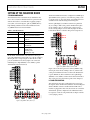
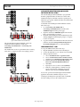
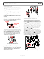
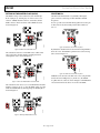
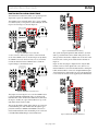
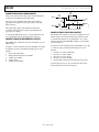
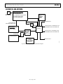
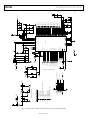
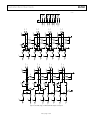
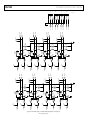
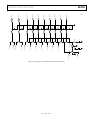
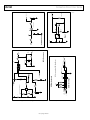
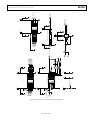
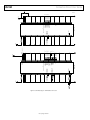
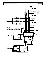
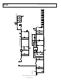
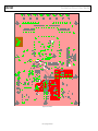
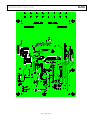
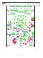
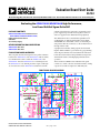
Evaluation Board User Guide
UG-564
ROUTING DIGITAL AUDIO CONNECTIONS
The ADAU196xA evaluation board has two separate inputs for
digital audio signals: the S/PDIF and the SDP interface.
11588-015
11588-017
The S/PDIF receiver can handle either of two options: S/PDIF
uses the RCA jack, J1, and optical uses the Toslink jack, U1. The
input is selected using S1 as shown in Figure 15.
Figure 15. S/PDIF Input Selector Switch SW1
Figure 17. S/PDIF Data and Clock Routing
The system development platform (SDP) interfaces, J6 and J8,
make up a standard interconnect within Analog Devices, Inc.
They provide for the transfer of digital audio clocks and control
between boards. See the pinout included in the schematic in
Figure 27.
A series of resistors have been provided to set the functional
mode of the S/PDIF receiver as shown in Figure 16. By default,
the S/PDIF receiver runs in master mode, 256 × fS, I2S format.
Consult the data sheet for the S/PDIF receiver to make the
required changes to the hardware mode.
11588-016
Figure 18 shows the jumper configuration for using the SDP
interface connector as the digital audio source. JP22 is set so
that the DSDATA1 source from the SDP interface is driving the
buffer, and this buffer is connected to all eight DSDATA inputs
of the ADAU196xA. JP10 and JP12 are set for the ADAU196xA
to run in slave mode from clocks supplied by the SDP interface.
Figure 16. S/PDIF Mode Selection Resistors
The pins in the middle column of these jumpers are connected
to the DSDATAx pins of the ADAU196xA through the appropriate line termination. DBCLK and DLRCLK selections are
made with JP10 and JP12 where the middle pins are connected
to the DBCLK and DLRCLK pins of the ADAU196xA.
Rev. 0 | Page 7 of 32
11588-018
The jumpers shown in Figure 17 are set for the S/PDIF receiver
to drive the DBCLK and DLRCLK clock ports and the eight
DSDATAx lines of the ADAU1962A/ADAU1966A. JP22 selects
the input to a buffer; the output of this buffer shows up on the
right-hand column of JP13 to JP20.
Figure 18. SDP Interface DSDATA1 Distribution