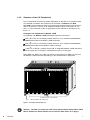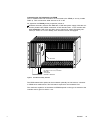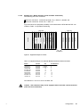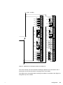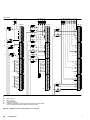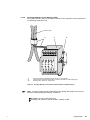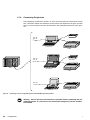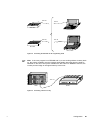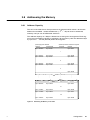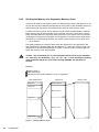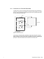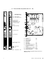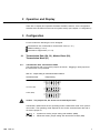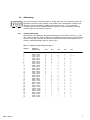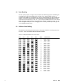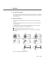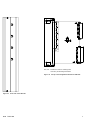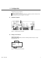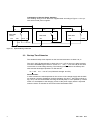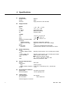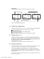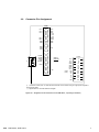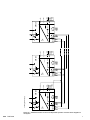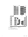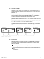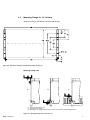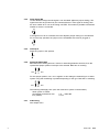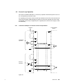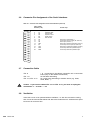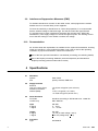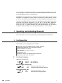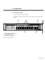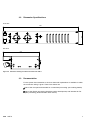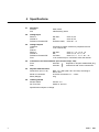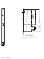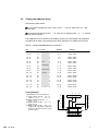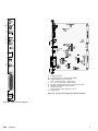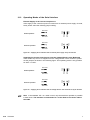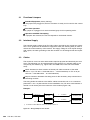
1
A500
Chassis Mount Controller
Standard Equipment
User Manual
A91M.12-279330.21-1191
Translation of the German Description
A91M.12-234802
Notes
Application Note
Caution The relevant regulations must be observed for control applications involving safety requirements.
For reasons of safety and to ensure compliance with documented system data,
repairs to components should be performed only by the manufacturer.
Training
AEG offers suitable training that provides further information concerning the system
(see addresses).
Data, Illustrations, Alterations
Data and illustrations are not binding. We reserve the right to alter our products in line
with our policy of continuous product development. If you have any suggestions for improvements or amendments or have found errors in this publication, please notify us by
using the form on the last page of this publication.
Addresses
The addresses of our Regional Sales Offices, Training Centers, Service and Engineering Sales Offices in Europe are given at the end of this publication.
Copyright
All rights reserved. No part of this document may be reproduced or transmitted in any
form or by any means, electronic or mechanical, including copying, processing or any
information storage, without permission in writing by the AEG Aktiengesellschaft. You
are not authorized to translate this document into any other language.
Trademarks
All terms used in this user manual to denote AEG products are trademarks of the AEG
Aktiengesellschaft.
IBM, IBM-PC, IBM-XT and IBM-AT are registered trademarks of International Business
Machines Corporation.
Microsoft and MS-DOS are registered trademarks of Microsoft Corporation.
© 1991 AEG Aktiengesellschaft.
ii
21
Terminology
Note
This symbol emphasizes very important facts.
Caution This symbol refers to frequently appearing error sources.
Warning This symbol points to sources of danger that may cause financial and
health damages or may have other aggravating consequences.
Expert This symbol is used when a more detailed information is given, which is intended exclusively for experts (special training required). Skipping this information does
not interfere with understanding the publication and does not restrict standard application of the product.
Path This symbol identifies the use of paths in software menus.
Figures are given in the spelling corresponding to international practice and approved
by SI (Système International d‘ Unités).
I.e. a space between the thousands and the usage of a decimal point (e.g.: 12 345.67).
Objectives
This publication is the basic publication for the A500. It describes the scope of performance of the programmable controller and supplies the user with all the information
which he requires in order to build it up so that he can start it for standard applications
and begin with the programming. The following is described:
Conciguration (combination of process, operating and programming peripherals)
Hardware structure
Port of the power supply
Port of the cable leading to the process
Procedure for the initial start-up
Cross references to the publications which involve special applications (e.g., system
communication, process visualization, programming, ...) are also given at suitable
places.
21
iii
Arrangement of This Guide
Chapter 1
General
This chapter lights on the integration of the Modicon A500 programmable controller in
its programming, operating, networking and I/O peripherals. The emphasis lies on the
question, “What is possible with the A500 and where do its performance limits lie?”
Concrete instructions for action are not given at this point; chapter 3 is concerned with
these in a thorough way.
The following points are treated in detail:
Structure (configuration limits, applicable hardware modules)
Networking possibilities with other programmable controllers
Connectable printers, programming and operating devices
Survey of the available software
Chapter 2
Operating and Indicating Elements
This chapter is only concerned with the topics which are relevant for the operator of an
A500 running in the process, divided according to operating and indicating elements as
well as simple maintenance works. It shows the possibilities concerning the structure of
an operator interface and supplies catch points which are significant for the compilation
of system-/application-specific operating instructions and maintenance schedules for the
Modicon A500.
Chapter 3
Configuration and System Start-Up
This chapter contains detailled configuration guides, hardware settings and installation
guidelines with notes for the system start-up.
Chapter 4
Characteristic Data
All the specifications of the A500 are summarized in this chapter according to the VDI
guideline 2880, page 1.
Chapter 5
Earthing and EMC Measures
This chapter imparts basic knowledge for earthing and EMC measures.
Appendix A
Programming in Dolog B
This chapter dealed with the generation and entry of Dolog B programs. It deals with
the following topics with special emphasis:
Program structure and program generation
Program entry
Operating time calculation
Appendix B
Module Descriptions
The descriptions of those modules which are used in the controller of the A500 can be
found in the appendix. The module descriptions of the I/O modules are summarized in
the user manual of the I/O peripherals with front connection.
iv
21
Related Documents
AEG offers a family of open-loop controllers which increase in the performance level
and are compatible in hardware and software over a wide range with the chassis mount
controllers A130, A350 and A500. These facts are taken into account in the documentation concept shown on the next page. The concept is divided into the four following
main areas.
Programmable Controllers
One user manual is provided for each controller of the individual programmable controllers. The user finds all the necessary information in this publication in order to prepare
the programmable controller so that he can start it up and begin the programming.
Process Peripherals
Concrete information concerning the structure of the process peripherals are given in a
total of three publications (linking the I/O subracks to the controller, linking the I/O subracks to each other, etc.). The description of those modules which are used to build up
the I/O peripherals (I/O modules, secondary subracks, power supplies, cables, ...) are
also summarized in the appendix.
Firmware
The software integrated in the central processing unit is documented in these publications.
Software for Programming Panels
The program packages which can be run on PCs and are obtainable as an option for
the programming and as a start-up aid of the PLC are described here. The relevant
software kits are sold as 3 1/2” and 5 1/4” diskettes.
21
v
Automation
device
(central part)
Process
periphery
A130
Modular Automation Device
A350
Modular Automation Device
A500
Modular Automation Device
A91V.12-234 585
A91V.12-234 678
A91M.12-279 330
DEA-H1, DEA-K1
Decentralized Extension
Assembly
for A030, A130 / A350 / A500
A91V.12-234 820
Process Peripherals
Front Connection Technology
for A130 / A350 / A500
Process Peripherals
Rear Connection Technology
for A350 / A500
A91V.12-271 613
A91V.12-
Programming Dolog A
for A030 / A130
Software
incorporated
in devices
A91V.12-
MMI Module and
Function
for A350 / A500
(TESY)
A91V.12-232 026
Device Couplings
for A350 / A500
Dolog B Regulations
for A350 / A500
A91V.12-234 731
Mass Flow,
Sequence Control
System
for A350 / A500
A91V.12-234 561
A91V.12-232 028
A91V.12-232 260
Dolog AKF
for A030 / A130
Dolog AKF
for A350 / A500
Dolog B
for A350 / A500
SW - Archiving
for A350/A500
Systems (Archives)
EDITOR
for A350 / A500
Systems
E-Nr. 424-247 139
E-Nr. 424-
E-Nr. 424-
E-Nr. 424-
E-Nr. 424-
MMI Editor for
A350 / A500
(TESY)
Designed Device
Coupling
for KOS 130
COM
E-Nr. 424-
Designed Device
Coupling
for A350 / A500
COM
E-Nr. 424-
Initial Operation
Assistance
for A350 / A500
SETUP LOOP CTRL.
E-Nr. 424-
INSTAL
for Programming
Unit
Dolog B Basic Module
for A350 / A500
Programming
device
software
Operating Functions
Bsdol B2
for A350 / A500
A91V.12-234 730
E-Nr. 424-
E-Nr. 424-
The following publication is not yet finished:
Process Peripherals
Rear Connection Technology
for A350 / A500
You only can obtain the German Edidion with the No. A91M.12-234 780 or you must order the predecessor:
Systemdescription
A500
Part 1-19
A91V.12-232 021
vi
21
Table of Contents
20
Chapter 1
General . . . . . . . . . . . . . . . . . . . . . . . . . . . . . . . . . . . . . . . . . . . . . . . . . . . . . . . . 1
1.1
1.2
1.3
1.3.1
1.3.2
1.3.3
1.3.4
1.4
1.4.1
1.4.1.1
1.4.1.2
1.4.1.3
1.4.1.4
1.4.2
1.4.3
1.5
1.5.1
1.5.2
1.5.3
1.6
1.6.1
1.6.2
1.6.3
1.6.4
1.6.5
1.7
1.7.1
1.7.2
1.7.3
1.7.4
1.7.5
1.8
1.9
1.10
Introduction . . . . . . . . . . . . . . . . . . . . . . . . . . . . . . . . . . . . . . . . . . . . . . . . . . . . . . . . . . . . . . . . . . 2
Compatibility . . . . . . . . . . . . . . . . . . . . . . . . . . . . . . . . . . . . . . . . . . . . . . . . . . . . . . . . . . . . . . . . . 2
General Mode of Operation . . . . . . . . . . . . . . . . . . . . . . . . . . . . . . . . . . . . . . . . . . . . . . . . . . . . 3
Memory . . . . . . . . . . . . . . . . . . . . . . . . . . . . . . . . . . . . . . . . . . . . . . . . . . . . . . . . . . . . . . . . . . . . . 3
Central Processing Unit . . . . . . . . . . . . . . . . . . . . . . . . . . . . . . . . . . . . . . . . . . . . . . . . . . . . . . . 4
I/O Modules . . . . . . . . . . . . . . . . . . . . . . . . . . . . . . . . . . . . . . . . . . . . . . . . . . . . . . . . . . . . . . . . . 4
Busses . . . . . . . . . . . . . . . . . . . . . . . . . . . . . . . . . . . . . . . . . . . . . . . . . . . . . . . . . . . . . . . . . . . . . 5
Structure . . . . . . . . . . . . . . . . . . . . . . . . . . . . . . . . . . . . . . . . . . . . . . . . . . . . . . . . . . . . . . . . . . . . 6
Standard Equipment for the Controller . . . . . . . . . . . . . . . . . . . . . . . . . . . . . . . . . . . . . . . . . . 6
STA 501, STA 551 . . . . . . . . . . . . . . . . . . . . . . . . . . . . . . . . . . . . . . . . . . . . . . . . . . . . . . . . . . . . 7
STA 503, STA 553 . . . . . . . . . . . . . . . . . . . . . . . . . . . . . . . . . . . . . . . . . . . . . . . . . . . . . . . . . . . . 7
STA 557 . . . . . . . . . . . . . . . . . . . . . . . . . . . . . . . . . . . . . . . . . . . . . . . . . . . . . . . . . . . . . . . . . . . . 7
STA 505, STA 555 . . . . . . . . . . . . . . . . . . . . . . . . . . . . . . . . . . . . . . . . . . . . . . . . . . . . . . . . . . . . 7
Structure of the I/O Peripherals . . . . . . . . . . . . . . . . . . . . . . . . . . . . . . . . . . . . . . . . . . . . . . . . 8
Configuration Limits . . . . . . . . . . . . . . . . . . . . . . . . . . . . . . . . . . . . . . . . . . . . . . . . . . . . . . . . 10
Recommended Peripherals . . . . . . . . . . . . . . . . . . . . . . . . . . . . . . . . . . . . . . . . . . . . . . . . . . . 11
Usable Programming Panels . . . . . . . . . . . . . . . . . . . . . . . . . . . . . . . . . . . . . . . . . . . . . . . . . 11
Usable Printers . . . . . . . . . . . . . . . . . . . . . . . . . . . . . . . . . . . . . . . . . . . . . . . . . . . . . . . . . . . . . 11
Devices to Program EPROMs . . . . . . . . . . . . . . . . . . . . . . . . . . . . . . . . . . . . . . . . . . . . . . . . 11
Programming . . . . . . . . . . . . . . . . . . . . . . . . . . . . . . . . . . . . . . . . . . . . . . . . . . . . . . . . . . . . . . 12
Program Generation . . . . . . . . . . . . . . . . . . . . . . . . . . . . . . . . . . . . . . . . . . . . . . . . . . . . . . . . 12
Programming Panels . . . . . . . . . . . . . . . . . . . . . . . . . . . . . . . . . . . . . . . . . . . . . . . . . . . . . . . 12
Special Programming Languages . . . . . . . . . . . . . . . . . . . . . . . . . . . . . . . . . . . . . . . . . . . . 13
Principle Structure of a Dolog AKF Program . . . . . . . . . . . . . . . . . . . . . . . . . . . . . . . . . . . 14
Principle Structure of a Dolog B Program . . . . . . . . . . . . . . . . . . . . . . . . . . . . . . . . . . . . . . 15
Networking . . . . . . . . . . . . . . . . . . . . . . . . . . . . . . . . . . . . . . . . . . . . . . . . . . . . . . . . . . . . . . . . 16
Overview . . . . . . . . . . . . . . . . . . . . . . . . . . . . . . . . . . . . . . . . . . . . . . . . . . . . . . . . . . . . . . . . . . 16
Modnet 1/SFB Communication . . . . . . . . . . . . . . . . . . . . . . . . . . . . . . . . . . . . . . . . . . . . . . . 17
Modnet 1/N Communication . . . . . . . . . . . . . . . . . . . . . . . . . . . . . . . . . . . . . . . . . . . . . . . . . 18
Modnet 1/F Communication . . . . . . . . . . . . . . . . . . . . . . . . . . . . . . . . . . . . . . . . . . . . . . . . . 18
Modnet 2/NP Communication . . . . . . . . . . . . . . . . . . . . . . . . . . . . . . . . . . . . . . . . . . . . . . . . 19
Tesy . . . . . . . . . . . . . . . . . . . . . . . . . . . . . . . . . . . . . . . . . . . . . . . . . . . . . . . . . . . . . . . . . . . . . . 19
Survey of the Usable Software Packages . . . . . . . . . . . . . . . . . . . . . . . . . . . . . . . . . . . . . 20
Module Survey . . . . . . . . . . . . . . . . . . . . . . . . . . . . . . . . . . . . . . . . . . . . . . . . . . . . . . . . . . . . . 21
Table of Contents
vii
Chapter 2
2.1
2.2
2.2.1
2.2.2
2.2.3
2.3
2.4
2.5
2.5.1
2.5.2
2.5.3
Indicating Elements . . . . . . . . . . . . . . . . . . . . . . . . . . . . . . . . . . . . . . . . . . . . . . . . . . . . . . . . .
Switches, Contact Sockets, Push Buttons . . . . . . . . . . . . . . . . . . . . . . . . . . . . . . . . . . . . .
Switches . . . . . . . . . . . . . . . . . . . . . . . . . . . . . . . . . . . . . . . . . . . . . . . . . . . . . . . . . . . . . . . . . .
Contact Sockets . . . . . . . . . . . . . . . . . . . . . . . . . . . . . . . . . . . . . . . . . . . . . . . . . . . . . . . . . . .
Push Buttons . . . . . . . . . . . . . . . . . . . . . . . . . . . . . . . . . . . . . . . . . . . . . . . . . . . . . . . . . . . . . .
Changing the Rechargable Battery (Maintenance) . . . . . . . . . . . . . . . . . . . . . . . . . . . . . .
Setting Up an Operator Interface . . . . . . . . . . . . . . . . . . . . . . . . . . . . . . . . . . . . . . . . . . . . .
Switching the Supply Voltage On and Off . . . . . . . . . . . . . . . . . . . . . . . . . . . . . . . . . . . . . .
The System is Switched On and Off by the User . . . . . . . . . . . . . . . . . . . . . . . . . . . . . . .
The System is Switched On and Off by a Powerfail . . . . . . . . . . . . . . . . . . . . . . . . . . . . .
Check Measures (Inspection) . . . . . . . . . . . . . . . . . . . . . . . . . . . . . . . . . . . . . . . . . . . . . . . .
26
28
28
28
28
29
30
31
31
31
31
Chapter 3
Configuration . . . . . . . . . . . . . . . . . . . . . . . . . . . . . . . . . . . . . . . . . . . . . . . . . 33
3.1
3.1.1
3.1.1.1
3.1.1.2
3.1.1.3
3.1.1.4
3.1.2
3.1.2.1
3.1.2.2
3.1.2.3
3.1.3
3.1.4
3.1.5
3.1.5.1
3.1.5.2
3.1.5.3
3.1.6
3.1.6.1
3.1.6.2
3.1.6.3
3.2
3.2.1
3.2.2
Configuration of the Hardware . . . . . . . . . . . . . . . . . . . . . . . . . . . . . . . . . . . . . . . . . . . . . . . 34
Structure of the Controller . . . . . . . . . . . . . . . . . . . . . . . . . . . . . . . . . . . . . . . . . . . . . . . . . . . 34
Structure of the Controller with the STA 501 / STA 551 . . . . . . . . . . . . . . . . . . . . . . . . . . 35
Structure of the Controller with the STA 503 / STA 553 . . . . . . . . . . . . . . . . . . . . . . . . . . 36
Structure of the Controller with the STA 505 / STA 555 . . . . . . . . . . . . . . . . . . . . . . . . . . 37
Structure of the Controller with the STA 557 . . . . . . . . . . . . . . . . . . . . . . . . . . . . . . . . . . . 38
Structure of the I/O Peripherals . . . . . . . . . . . . . . . . . . . . . . . . . . . . . . . . . . . . . . . . . . . . . . 39
Structure of the I/O Peripheral with Front Connection . . . . . . . . . . . . . . . . . . . . . . . . . . . 39
Structure of the I/O Peripherals with Rear Connection . . . . . . . . . . . . . . . . . . . . . . . . . . 42
Mixed Structure . . . . . . . . . . . . . . . . . . . . . . . . . . . . . . . . . . . . . . . . . . . . . . . . . . . . . . . . . . . . 45
Configuration Limits (Maximum Expansion) . . . . . . . . . . . . . . . . . . . . . . . . . . . . . . . . . . . . 46
Specifying the I/O Equipment . . . . . . . . . . . . . . . . . . . . . . . . . . . . . . . . . . . . . . . . . . . . . . . . 48
Specifying the Slot References . . . . . . . . . . . . . . . . . . . . . . . . . . . . . . . . . . . . . . . . . . . . . . 48
Specifying the Slot References with Front Connection . . . . . . . . . . . . . . . . . . . . . . . . . . 48
Specifying the Slot References with Rear Connection . . . . . . . . . . . . . . . . . . . . . . . . . . . 49
Example for a Mixed Structure (Front and Rear Connection) . . . . . . . . . . . . . . . . . . . . . 51
Assignment of the Signal Addresses to the Signals (Addressing) . . . . . . . . . . . . . . . . . 52
Addressing According to DIN . . . . . . . . . . . . . . . . . . . . . . . . . . . . . . . . . . . . . . . . . . . . . . . . 52
AEG Addressing . . . . . . . . . . . . . . . . . . . . . . . . . . . . . . . . . . . . . . . . . . . . . . . . . . . . . . . . . . . 54
Symbolic Addressing . . . . . . . . . . . . . . . . . . . . . . . . . . . . . . . . . . . . . . . . . . . . . . . . . . . . . . . 55
Structure of the Power Supplies . . . . . . . . . . . . . . . . . . . . . . . . . . . . . . . . . . . . . . . . . . . . . . 56
Supplying the Supply and Working Voltages for I/O Modules with Rear Connection . 58
Port Diagram of the UB Supply (24 VDC for Modules and Sensors) with I/O Modules
with Front Connection . . . . . . . . . . . . . . . . . . . . . . . . . . . . . . . . . . . . . . . . . . . . . . . . . . . . . . 58
Port Figure of the Working Voltage Supply (US = 24 VDC / L = 230 VAC) for I/O
Modules with Front Connection . . . . . . . . . . . . . . . . . . . . . . . . . . . . . . . . . . . . . . . . . . . . . . 65
Switching Off Mode of the Binary Outputs with Malfunctions on the Power Supply . . 70
Switching Off Mode for Modules with Rear Connection . . . . . . . . . . . . . . . . . . . . . . . . . . 70
Switching Off Mode for Modules with Front Connection . . . . . . . . . . . . . . . . . . . . . . . . . 71
Synchronization of the Power Supplies . . . . . . . . . . . . . . . . . . . . . . . . . . . . . . . . . . . . . . . . 72
PEAB Monitoring . . . . . . . . . . . . . . . . . . . . . . . . . . . . . . . . . . . . . . . . . . . . . . . . . . . . . . . . . . . 72
Start-Up Characteristics . . . . . . . . . . . . . . . . . . . . . . . . . . . . . . . . . . . . . . . . . . . . . . . . . . . . . 74
Start-Up Characteristics when Using the ALU 011 . . . . . . . . . . . . . . . . . . . . . . . . . . . . . . 74
Start-Up Characteristics when Using the ALU 061 . . . . . . . . . . . . . . . . . . . . . . . . . . . . . . 74
Start-Up Characteristics when Using the ALU 150 . . . . . . . . . . . . . . . . . . . . . . . . . . . . . . 75
3.2.3
3.3
3.3.1
3.3.2
3.4
3.5
3.6
3.6.1
3.6.2
3.6.3
viii
Operating . . . . . . . . . . . . . . . . . . . . . . . . . . . . . . . . . . . . . . . . . . . . . . . . . . . . . 25
Table of Contents
20
20
3.7
3.7.1
3.7.2
3.7.3
3.7.3.1
3.7.3.2
3.7.3.3
3.7.3.4
3.7.4
3.8
3.8.1
3.8.2
3.8.3
3.8.4
3.8.5
3.8.6
3.8.7
3.9
3.9.1
3.9.2
3.9.3
3.10
3.10.1
3.10.2
3.10.3
3.10.4
3.11
3.11.1
3.11.2
3.11.3
Installation . . . . . . . . . . . . . . . . . . . . . . . . . . . . . . . . . . . . . . . . . . . . . . . . . . . . . . . . . . . . . . . . . 76
Settings for Modules . . . . . . . . . . . . . . . . . . . . . . . . . . . . . . . . . . . . . . . . . . . . . . . . . . . . . . . . 76
Mounting and Equipping the Subracks . . . . . . . . . . . . . . . . . . . . . . . . . . . . . . . . . . . . . . . . 79
Discharge Measures . . . . . . . . . . . . . . . . . . . . . . . . . . . . . . . . . . . . . . . . . . . . . . . . . . . . . . . . 80
Discharge Measures for Analogue Shielded Cables . . . . . . . . . . . . . . . . . . . . . . . . . . . . 80
Discharge Measure for the Modnet 1/SFB . . . . . . . . . . . . . . . . . . . . . . . . . . . . . . . . . . . . . 81
Improving the EMC Immunity for the Modules . . . . . . . . . . . . . . . . . . . . . . . . . . . . . . . . . 83
Overvoltage Protection for SFB Lines: Outside Buildings . . . . . . . . . . . . . . . . . . . . . . . . 84
Connecting Peripheries . . . . . . . . . . . . . . . . . . . . . . . . . . . . . . . . . . . . . . . . . . . . . . . . . . . . . 86
Addressing the Memory . . . . . . . . . . . . . . . . . . . . . . . . . . . . . . . . . . . . . . . . . . . . . . . . . . . . . 88
Address Capacity . . . . . . . . . . . . . . . . . . . . . . . . . . . . . . . . . . . . . . . . . . . . . . . . . . . . . . . . . . 88
Dividing the Memory into Segments, Memory Areas . . . . . . . . . . . . . . . . . . . . . . . . . . . . 89
Occupation of the Segments when Using ALU 150 . . . . . . . . . . . . . . . . . . . . . . . . . . . . . 90
Occupation of the Segments when Using the ALU 011 or ALU 061 . . . . . . . . . . . . . . . 90
Segments 1 and 2, Signal Memory . . . . . . . . . . . . . . . . . . . . . . . . . . . . . . . . . . . . . . . . . . . 91
Special Marker Area . . . . . . . . . . . . . . . . . . . . . . . . . . . . . . . . . . . . . . . . . . . . . . . . . . . . . . . . 92
Special Word, Double Word and Floating Point Word Area . . . . . . . . . . . . . . . . . . . . . . 93
Check List for the Initial Start-Up and Test . . . . . . . . . . . . . . . . . . . . . . . . . . . . . . . . . . . . . 95
Settings, Ports, Equipment . . . . . . . . . . . . . . . . . . . . . . . . . . . . . . . . . . . . . . . . . . . . . . . . . . 95
Information About the Initial State Disable (G Plug-In Jumper on the UKA) . . . . . . . . 96
Initial Start-Up . . . . . . . . . . . . . . . . . . . . . . . . . . . . . . . . . . . . . . . . . . . . . . . . . . . . . . . . . . . . . 97
Further Information . . . . . . . . . . . . . . . . . . . . . . . . . . . . . . . . . . . . . . . . . . . . . . . . . . . . . . . . . 98
Information to Enter the Equipment in the Equipment List . . . . . . . . . . . . . . . . . . . . . . . 98
PEAB Time Error . . . . . . . . . . . . . . . . . . . . . . . . . . . . . . . . . . . . . . . . . . . . . . . . . . . . . . . . . . . 99
Watchdog Display - Signal Relay - Marker 60 . . . . . . . . . . . . . . . . . . . . . . . . . . . . . . . . . 100
Setting the Transmission Rate with the Software . . . . . . . . . . . . . . . . . . . . . . . . . . . . . . 100
Documentation and Archiving . . . . . . . . . . . . . . . . . . . . . . . . . . . . . . . . . . . . . . . . . . . . . . . 101
Documentation of the Hardware Settings . . . . . . . . . . . . . . . . . . . . . . . . . . . . . . . . . . . . . 101
Documentation of the User Program with Additional Information . . . . . . . . . . . . . . . . . 104
Program Archiving . . . . . . . . . . . . . . . . . . . . . . . . . . . . . . . . . . . . . . . . . . . . . . . . . . . . . . . . . 104
Chapter 4
Specifications . . . . . . . . . . . . . . . . . . . . . . . . . . . . . . . . . . . . . . . . . . . . . . . 105
4.1
4.2
4.2.1
4.2.2
4.2.2.1
4.2.2.2
4.2.2.3
4.2.3
4.2.3.1
4.2.3.2
4.2.3.3
4.2.3.4
4.2.3.5
4.2.3.6
4.2.3.7
4.3
4.4
4.5
4.5.1
4.5.2
4.5.3
4.5.4
User Program . . . . . . . . . . . . . . . . . . . . . . . . . . . . . . . . . . . . . . . . . . . . . . . . . . . . . . . . . . . . . 106
Interfaces . . . . . . . . . . . . . . . . . . . . . . . . . . . . . . . . . . . . . . . . . . . . . . . . . . . . . . . . . . . . . . . . 107
Supply Interface . . . . . . . . . . . . . . . . . . . . . . . . . . . . . . . . . . . . . . . . . . . . . . . . . . . . . . . . . . . 107
Process Interfaces . . . . . . . . . . . . . . . . . . . . . . . . . . . . . . . . . . . . . . . . . . . . . . . . . . . . . . . . 107
Configuration Limits . . . . . . . . . . . . . . . . . . . . . . . . . . . . . . . . . . . . . . . . . . . . . . . . . . . . . . . 107
Inputs . . . . . . . . . . . . . . . . . . . . . . . . . . . . . . . . . . . . . . . . . . . . . . . . . . . . . . . . . . . . . . . . . . . . 108
Outputs . . . . . . . . . . . . . . . . . . . . . . . . . . . . . . . . . . . . . . . . . . . . . . . . . . . . . . . . . . . . . . . . . . 109
Data Intereface . . . . . . . . . . . . . . . . . . . . . . . . . . . . . . . . . . . . . . . . . . . . . . . . . . . . . . . . . . . 110
RS 232 C (V.24) Programming Interface . . . . . . . . . . . . . . . . . . . . . . . . . . . . . . . . . . . . . 110
Communications Port (RS 232 C / Current Loop / Telecontrol Mode) . . . . . . . . . . . . . 110
RS 485 Communications Port (Modnet 1/SFB) . . . . . . . . . . . . . . . . . . . . . . . . . . . . . . . . . 111
PMB (Parallel Microprocessor Bus) . . . . . . . . . . . . . . . . . . . . . . . . . . . . . . . . . . . . . . . . . . . 111
PEAB (Parallel I/O Bus) . . . . . . . . . . . . . . . . . . . . . . . . . . . . . . . . . . . . . . . . . . . . . . . . . . . . . 111
PAB 1 (Parallel System Bus) . . . . . . . . . . . . . . . . . . . . . . . . . . . . . . . . . . . . . . . . . . . . . . . . . 111
PLB (Parallel Local Bus) . . . . . . . . . . . . . . . . . . . . . . . . . . . . . . . . . . . . . . . . . . . . . . . . . . . 112
Processor . . . . . . . . . . . . . . . . . . . . . . . . . . . . . . . . . . . . . . . . . . . . . . . . . . . . . . . . . . . . . . . . 112
Processing Times . . . . . . . . . . . . . . . . . . . . . . . . . . . . . . . . . . . . . . . . . . . . . . . . . . . . . . . . . 113
Memories . . . . . . . . . . . . . . . . . . . . . . . . . . . . . . . . . . . . . . . . . . . . . . . . . . . . . . . . . . . . . . . . 113
Signal and System Memory . . . . . . . . . . . . . . . . . . . . . . . . . . . . . . . . . . . . . . . . . . . . . . . . 113
Memory for the Basic Software . . . . . . . . . . . . . . . . . . . . . . . . . . . . . . . . . . . . . . . . . . . . . 113
Memory for the User Program . . . . . . . . . . . . . . . . . . . . . . . . . . . . . . . . . . . . . . . . . . . . . . 113
Backup Rechargable Battery . . . . . . . . . . . . . . . . . . . . . . . . . . . . . . . . . . . . . . . . . . . . . . . 114
Table of Contents
ix
4.6
4.6.1
4.6.2
4.6.3
4.7
4.7.1
4.7.2
4.7.3
Chapter 5
5.1
5.1.1
5.1.2
5.1.3
5.1.4
5.1.5
5.2
5.2.1
5.2.1.1
5.2.1.2
5.2.1.3
5.2.2
5.2.3
5.2.4
5.3
5.4
5.4.1
5.4.2
5.5
Physical Characteristics . . . . . . . . . . . . . . . . . . . . . . . . . . . . . . . . . . . . . . . . . . . . . . . . . . . .
Design Data . . . . . . . . . . . . . . . . . . . . . . . . . . . . . . . . . . . . . . . . . . . . . . . . . . . . . . . . . . . . . .
Permitted Line Lengths . . . . . . . . . . . . . . . . . . . . . . . . . . . . . . . . . . . . . . . . . . . . . . . . . . . .
Connection Mode . . . . . . . . . . . . . . . . . . . . . . . . . . . . . . . . . . . . . . . . . . . . . . . . . . . . . . . . .
Environmental Data . . . . . . . . . . . . . . . . . . . . . . . . . . . . . . . . . . . . . . . . . . . . . . . . . . . . . . .
Climatic (According to DIN 40 040, Page 1/6.70) . . . . . . . . . . . . . . . . . . . . . . . . . . . . . .
Mechanical (Shocks and Vibrations) . . . . . . . . . . . . . . . . . . . . . . . . . . . . . . . . . . . . . . . . .
Electrical . . . . . . . . . . . . . . . . . . . . . . . . . . . . . . . . . . . . . . . . . . . . . . . . . . . . . . . . . . . . . . . . .
114
114
115
115
116
116
116
117
Earthing and EMC-Measures . . . . . . . . . . . . . . . . . . . . . . . . . . . . . . . . . . 119
Earth Grounding and Earthing (Installation Guidelines) . . . . . . . . . . . . . . . . . . . . . . . . .
Earth Grounding All Inactive Metal Parts . . . . . . . . . . . . . . . . . . . . . . . . . . . . . . . . . . . . .
Protective Earthing According to VDE 0100 . . . . . . . . . . . . . . . . . . . . . . . . . . . . . . . . . .
Functional Earthing . . . . . . . . . . . . . . . . . . . . . . . . . . . . . . . . . . . . . . . . . . . . . . . . . . . . . . . .
Reference Conductor System . . . . . . . . . . . . . . . . . . . . . . . . . . . . . . . . . . . . . . . . . . . . . . .
Earthing System Measures for the Cabinet Structure . . . . . . . . . . . . . . . . . . . . . . . . . .
EMC Measures . . . . . . . . . . . . . . . . . . . . . . . . . . . . . . . . . . . . . . . . . . . . . . . . . . . . . . . . . . .
Measures for the Installation and Wiring . . . . . . . . . . . . . . . . . . . . . . . . . . . . . . . . . . . . .
Within a Cabinet . . . . . . . . . . . . . . . . . . . . . . . . . . . . . . . . . . . . . . . . . . . . . . . . . . . . . . . . . .
Outside Cabinets in Closed Buildings . . . . . . . . . . . . . . . . . . . . . . . . . . . . . . . . . . . . . . . .
Outside Buildings . . . . . . . . . . . . . . . . . . . . . . . . . . . . . . . . . . . . . . . . . . . . . . . . . . . . . . . . .
Measures for the Power Supply . . . . . . . . . . . . . . . . . . . . . . . . . . . . . . . . . . . . . . . . . . . . .
Measures Against Direct Noise Interference . . . . . . . . . . . . . . . . . . . . . . . . . . . . . . . . . .
Measures for the Sources of Interference . . . . . . . . . . . . . . . . . . . . . . . . . . . . . . . . . . . .
Interference Suppression . . . . . . . . . . . . . . . . . . . . . . . . . . . . . . . . . . . . . . . . . . . . . . . . . . .
Technique of Peripheral Ports . . . . . . . . . . . . . . . . . . . . . . . . . . . . . . . . . . . . . . . . . . . . . . .
Protective Circuits for Actuators . . . . . . . . . . . . . . . . . . . . . . . . . . . . . . . . . . . . . . . . . . . . .
Wiring the Reference Conductor in an Isolated Structure . . . . . . . . . . . . . . . . . . . . . . .
Protective Logic and Safety Interlocks . . . . . . . . . . . . . . . . . . . . . . . . . . . . . . . . . . . . . . .
120
120
120
121
121
123
124
124
124
126
126
127
127
127
128
128
128
129
130
Appendix A Programming in Dolog B . . . . . . . . . . . . . . . . . . . . . . . . . . . . . . . . . . . . . 131
A.1
A.1.1
A.1.2
A.1.2.1
A.1.2.2
A.1.3
A.1.4
A.2
A.3
A.4
A.4.1
A.4.2
A.4.3
A.4.4
A.5
A.6
x
Table of Contents
Construction of a Dolog B Program (VList Wiring/Connection List) . . . . . . . . . . . . . . .
Construction of a Linear VList . . . . . . . . . . . . . . . . . . . . . . . . . . . . . . . . . . . . . . . . . . . . . .
Structure of a VList With Jumps . . . . . . . . . . . . . . . . . . . . . . . . . . . . . . . . . . . . . . . . . . . . .
A Part of the VList is Skipped Depending on a Condition . . . . . . . . . . . . . . . . . . . . . . .
A Part of the VList is Run Depending on a Condition . . . . . . . . . . . . . . . . . . . . . . . . . .
Construction of a VList with Subroutines . . . . . . . . . . . . . . . . . . . . . . . . . . . . . . . . . . . . .
Interrupt VList . . . . . . . . . . . . . . . . . . . . . . . . . . . . . . . . . . . . . . . . . . . . . . . . . . . . . . . . . . . . .
Program Input . . . . . . . . . . . . . . . . . . . . . . . . . . . . . . . . . . . . . . . . . . . . . . . . . . . . . . . . . . . .
Measures to Take when the Program Crashes . . . . . . . . . . . . . . . . . . . . . . . . . . . . . . . .
List of Bsdol Functions (in order of their logical use) . . . . . . . . . . . . . . . . . . . . . . . . . . .
Online Parameters . . . . . . . . . . . . . . . . . . . . . . . . . . . . . . . . . . . . . . . . . . . . . . . . . . . . . . . .
Online Programming . . . . . . . . . . . . . . . . . . . . . . . . . . . . . . . . . . . . . . . . . . . . . . . . . . . . . . .
Online Testing . . . . . . . . . . . . . . . . . . . . . . . . . . . . . . . . . . . . . . . . . . . . . . . . . . . . . . . . . . . .
Online Documenting . . . . . . . . . . . . . . . . . . . . . . . . . . . . . . . . . . . . . . . . . . . . . . . . . . . . . . .
List of the Bsdol Functions (sorted topicwise) . . . . . . . . . . . . . . . . . . . . . . . . . . . . . . . . .
List of Dolog B Blocks . . . . . . . . . . . . . . . . . . . . . . . . . . . . . . . . . . . . . . . . . . . . . . . . . . . . .
132
132
133
133
134
135
136
137
138
139
139
140
141
141
143
145
20
A.7
A.7.1
A.7.2
A.7.3
A.7.4
A.7.5
A.7.6
Cycle Time . . . . . . . . . . . . . . . . . . . . . . . . . . . . . . . . . . . . . . . . . . . . . . . . . . . . . . . . . . . . . . .
Structure of the Program Cycle . . . . . . . . . . . . . . . . . . . . . . . . . . . . . . . . . . . . . . . . . . . . .
Delay Time of the END Block (or Program End in Dolog AKF) . . . . . . . . . . . . . . . . . .
Delay Time of Direct Binary and Analogue I/O on the Modnet 1/SFB . . . . . . . . . . . .
Processing of the END block for Dolog B or of the program end for Dolog AKF . . .
Notes on the Regulating Delay Time System . . . . . . . . . . . . . . . . . . . . . . . . . . . . . . . . .
Delay Times of the Dolog B Blocks (for ALU 150) . . . . . . . . . . . . . . . . . . . . . . . . . . . . .
151
151
152
153
154
155
156
Appendix B Module Descriptions . . . . . . . . . . . . . . . . . . . . . . . . . . . . . . . . . . . . . . . . . 165
ALU 011, ALU 012, ALU 021 Central Processing Unit . . . . . . . . . . . . . . . . . . . . . . . . . .
ALU 061, ALU 071 Central Processing Unit . . . . . . . . . . . . . . . . . . . . . . . . . . . . . . . . . .
ALU 150 Central Processing Unit . . . . . . . . . . . . . . . . . . . . . . . . . . . . . . . . . . . . . . . . . . .
BATT 3.6 - 1.8 Ah Rechargable Battery . . . . . . . . . . . . . . . . . . . . . . . . . . . . . . . . . . . . . .
BIK 151 Modnet 1/SFB Interface for Central Processing Units . . . . . . . . . . . . . . . . . .
COP 82Coprocessor . . . . . . . . . . . . . . . . . . . . . . . . . . . . . . . . . . . . . . . . . . . . . . . . . . . . . . .
DKV 023 PEAB Network . . . . . . . . . . . . . . . . . . . . . . . . . . . . . . . . . . . . . . . . . . . . . . . . . . .
DNO 028 24 VDC Power Supply . . . . . . . . . . . . . . . . . . . . . . . . . . . . . . . . . . . . . . . . . . . .
DNP 023 220 VAC Power Supply . . . . . . . . . . . . . . . . . . . . . . . . . . . . . . . . . . . . . . . . . . .
DNP 023-1, DNP 023-2 Power Supply . . . . . . . . . . . . . . . . . . . . . . . . . . . . . . . . . . . . . . .
DNP 023-3, DNP 023-4 Power Supply . . . . . . . . . . . . . . . . . . . . . . . . . . . . . . . . . . . . . . .
DNP 028 220 VAC Power Supply . . . . . . . . . . . . . . . . . . . . . . . . . . . . . . . . . . . . . . . . . . .
DTA 024 Subrack . . . . . . . . . . . . . . . . . . . . . . . . . . . . . . . . . . . . . . . . . . . . . . . . . . . . . . . . .
DTA 27.1 Subrack . . . . . . . . . . . . . . . . . . . . . . . . . . . . . . . . . . . . . . . . . . . . . . . . . . . . . . . . .
DTA 028 Subrack . . . . . . . . . . . . . . . . . . . . . . . . . . . . . . . . . . . . . . . . . . . . . . . . . . . . . . . . .
DTA 101 Subrack . . . . . . . . . . . . . . . . . . . . . . . . . . . . . . . . . . . . . . . . . . . . . . . . . . . . . . . . .
DTA 107 Subrack . . . . . . . . . . . . . . . . . . . . . . . . . . . . . . . . . . . . . . . . . . . . . . . . . . . . . . . . .
KOS 152 Modnet 1N Interface . . . . . . . . . . . . . . . . . . . . . . . . . . . . . . . . . . . . . . . . . . . . . .
KOS 882 Communication Processor . . . . . . . . . . . . . . . . . . . . . . . . . . . . . . . . . . . . . . . . .
LLB Air Guide . . . . . . . . . . . . . . . . . . . . . . . . . . . . . . . . . . . . . . . . . . . . . . . . . . . . . . . . . . . .
MAT 827 Arithmetic Processor . . . . . . . . . . . . . . . . . . . . . . . . . . . . . . . . . . . . . . . . . . . . . .
SAE 2 Cabinet Connection Unit . . . . . . . . . . . . . . . . . . . . . . . . . . . . . . . . . . . . . . . . . . . . .
SC 8128 / SC 8256 Memory Module (RAM) . . . . . . . . . . . . . . . . . . . . . . . . . . . . . . . . . .
SF 8512 Memory Module (EPROM) . . . . . . . . . . . . . . . . . . . . . . . . . . . . . . . . . . . . . . . . .
UKA 024 Monitoring Module . . . . . . . . . . . . . . . . . . . . . . . . . . . . . . . . . . . . . . . . . . . . . . . .
UVL 841, UVL 842 Interface Converter . . . . . . . . . . . . . . . . . . . . . . . . . . . . . . . . . . . . . . .
20
Table of Contents
167
155
177
221
225
235
243
249
257
265
275
285
293
301
313
323
333
347
361
369
373
379
385
391
397
413
xi
xii
Table of Contents
20
Chapter 1
General
This chapter lights on the integration of the Modicon A500 programmable controller in its programming, operating, networking and I/O peripherals. The emphasis lies on the question, “What is possible with the
A500” and where do its performance limit lie?”. Concrete instructions for
action are not given at this point; chapter 3 is concerned with these in a
thorough way.
The following points are treated in detail:
Structure (configuration limits, applicable hardware modules)
Obtainable standard versions
Networking possibilities with other programmable controllers
Connectable printers, programming and operating devices
Survey of the available software
21
General
1
1.1 Introduction
Modicon A500 is a chassis mount controller for medium to larger automation tasks. It
allows the following automation functions depending on the configuration degree:
Control
Closed-loop control
Computing
Processing the measured values
Signalling, monitoring
Log
Visual display (Viewstar 200 / Viewstar B500)
Text dialogue (Tesy)
Communication
Modicon A500 is mounted in subracks which are designed for applications with poor
ambient conditions (rigid structure). Slots are prepared on them in which the individual
modules are inserted via guide rails. The chassis earth is connected and the modules
are connected to the bus system of the A500 automatically here.
Subracks with a breadth of 1/2 19” and 19” are available. The installed height of all the
subracks amounts to 6 height units for all of them whereby 1 height unit is 44.45 mm
high.
The A500 can have a front connection or a rear connection. All the ports are on the
front of the modules for the front connection. This allows the subracks to be mounted
on a wall as well as in 19” holders. The ports are on the rear of the subracks for the
rear connection. The subracks are then to be fixed in 19” holders.
The subracks with front connection include front covers which can be swong to both
sides and removed completely and which allow a view of the LED indicators of the
modules and can be individually fitted with insertable fill-in lables for the terminal assignment. The labelling is maintained when the modules are changed.
1.2 Compatibility
Hardware
The intelligent function module ZAE 105 and VIP 101 can also be inserted in A250 and
A350; I/O modules with front connection can also be inserted in A130, A250 and A350.
The prerequisite for uniform I/O peripherals from A130 to A500 was thus fulfilled. The
user now has the possibility to retrofit his machine from A130 via A250 and A350 to
A500 by changing the controllers without having to change the I/O peripherals.
Software
The performance of the basic software integrated in Modicon A350 is upwards compatible with Modicon A500. The software for programming panels which can be obtained
as an option is identical for both programmable controllers.
2
General
21
1.3 General Mode of Operation
The mode of operation of the A500 (cf. Figure 1) is greatly determined by the combination of:
Memory
Central processing unit
I/O modules
The flow of information between these components is safeguared by busses.
Memory
Signalmemory
Basicsoftware
I/O bit
Marker
Words
Double words
Floating point
words
e.g.
Bsdol 82
operating
communication
system
Central processing unit
(ALU 150 or ALU 0x1
PMB data
PMB
Processor
PMB
Modnet 1/SFBnetwork
(BIK 151/BIK 812)
Programs
PMB
PEAB
Dolog B
Tesy
etc.
Programs
Tesy texts
etc.
Input/
output
module
Process
Input/
output
module
Process
Serial
Interface
Networking
tables
PMB
Usersoftware
Modnet 1/SFB
(to UKA024 or to
ALU 0x1
Operaiting or
programming
devices
Figure 1
Mode of Operation of the A500 (Diagrammatic Representation)
1.3.1
Memory
The memory has an address space of 1 mbyte. A disctinction is made here between 3
areas:
User memory (RAM or EPROM)
Signal memory (RAM)
Basic software (EPROM)
The user memory makes available the memory space for the user program, for special
functions and for the system RAM. The user program can be saved on EPROM or on
RAM selectively.
The central processing unit itself is the carrier modules for the user memory when the
ALU 0x1 is used. Separate memory modules (SF 8512 (EPROM) or SC 8128 or
SC 8256 (RAM)) are necessary when the ALU 150 is used.
21
General
3
The process image (I/O bits, markers, words, double words and floating point words)
are saved in the signal memory. User programs always work with the data from the signal memory and not with the input and output signals themselves.
The basic software is located on EPROMs in the central processing unit. It includes all
the programs necessary for the programming and operation. This includes the Bsdol
operating communication system and the Dolog programming language, for example (in
the Dolog B programming type, i.e., log programming).
1.3.2
Central Processing Unit
The central processing unit is the processor of the A500. It controls the functions of the
entire system and executes the individual instructions of a program in accordance with
the rules pregiven by the basic software. It organizes the reading in of external data
and signals into the signal memory, processes these data and performs design calculations, continually deposites processing results in the signal memory and realizes the
output of the results.
User programs are always processed cyclically in the A500. The valences of the input
signals are read into the signal memory once at the end of each program cycle and the
valencies of the output signals output from the signal memory to the peripherals. The
user program always works with the data from the signal memory, i.e., with the process
images, only during the remainder of the program cycle.
This can be changed with the hardware module SES 2 (rear connection), for example.
A spontaneous entry, i.e., roughly free if delay, of preferably time-critical process signals can be forced with it using interrupt Another possibility for a delay-free input/output
is supplied by the software blocks of ”AUS”, “EIN”, “BAUS” and “BEIN”.
1.3.3
I/O Modules
All modules which have a direct effect on the process are I/O modules. This includes
the following:
Input/output modules for processing binary signal statuses
Input/output modules for processing analogue signals
Intelligent modules (partly autonomous I/O modules with an integrated processor,
e.g., back-up controller, positioning device, counter modules, etc.)
A distinction is to be made for the I/O modules:
Modules with front connection:
The process signals and the supply of the sensors and actuators are connected via
screw/plug-in terminals with front connections.
Modules with rear connection:
The process signals and the supply of the sensors and actuators are connected via
48 pole connectors which are located on the rear of the module.
A summary of all the modules which can be used for A500 and therefore also all the I/
O modules which can be used divided according to front and rear connection is given
by section 1.10.
4
General
21
1.3.4
Busses
The modules communicate with the central processing unit (ALU) via busses. The modules contact the bus/busses automatically when the modules are engaged via connectors arranged on the rear of the module board.
The PMB is a parallel microprocessor bus (memory bus) which is located on the rear
wall of the primary subrack. The central processing units (e.g., ALU 150), the memory
modules (SC 8256, SF 8512), the monitoring module (UKA 024) and the interface modules (BIK, KOS, KP, ...) are connected to it. Each PMB node occupies a certain part of
the available address space (memory). The definition of which addresses are assigned
to the respective node is given on the individual modules by the hardware via jumper
settings (no referencing). The jumper settings are to be taken from the individual module descriptions.
The Modnet 1/SFB is a serial data bus which creates the connection between the controller and the remote I/O peripherals. The modules with front connection (binary I/O,
analogue I/O and intelligend modules) can be operated using it.
A fixed slot reference is assigned to each I/O slot via jumpers. The addressing is therefore independent of the module with which the respective slot is equipped (referencing).
This bus has another field of application as a link. It can be used here to construct a
data path between two systems to be linked.
The PEAB is a parallel I/O bus which is located on the rear wall of the primary subrack
and of the secondary subrack, DTA 025. PEAB nodes are UKA 024, ALU 011,
ALU 061, ALU 150 and the I/O modules designed with rear connection and listed in
table Table 8. The I/O slots for the PEAB are located in the secondary subracks, DTA
025 and in the primary subracks DTA 024 and DTA 028.
A fixed slot reference must be assigned to each PEAB slot. The addressing is therefore
independent of the module with which the respective slot is equipped (referencing). The
addresses for ALU and UKA are given automatically by the system.
21
General
5
1.4 Structure
The Modicon A500 consists of a controller and the I/O peripherals, i.e., one of a
number of I/O modules depending on the task. It can be put together in a specific way
for the relevant application due to its modular structure.
The following pages help to clarify the construction principle of the A500. Section 3.1
gives more detailled information.
The controller of an A500 consists of a primary subrack which can be equipped with
modules which have the following functions:
Power supply (DNP ...)
Central processing unit (ALU 150, ALU 011 or ALU 061)
Monitoring module UKA 024 (only required with ALU 150)
Memory module (SF, SC, only required with ALU 150)
PMB node such as BIK, KOS, KP1-..., ... (optional, depends on the task)
PEAB-area
Figure 2
1.4.1
PMB-area
Modicon A500 with Rear Connection, Equipped with PMB and PEAB Nodes
Standard Equipment for the Controller
Partly equipped standard equipment which is to be expanded with memory modules
and the I/O peripherals can be obtained for standard applications They are ready for
the connection, i.e., preset and inspected both module by module and as a complete
unit.
The standard equipment can be supplied selectively with German or English basic software. Only the standard equipment with German basic software is described in this
manual.
6
General
21
A selection can be made between the following pieces of standard equipment depending on the task. Features in common and differences are summarized in Table 1.
Table 1
1.4.1.1
STA 501, STA 551
The standard equipment of STA 501 and STA 551 can be used for A500 systems which
require many PMB slots. They differ from each other due to the primary voltage of the
power supply (24 VDC for the STA 501, 230 VAC with the STA 551).
1.4.1.2
STA 503, STA 553
The standard equipment of STA 501 and STA 551 is meant for A500 systems which require a low number of PMB slots. They differ from each other due to the primary voltage of the power supply (24 VDC with the STA 503, 230 VAC with the STA 553). The
STA 553 has 3 PEAB slots less than the STA 503 due to the wider power supply.
1.4.1.3
STA 557
The standard equipment of STA 557 can be used when B500 is to be employed. It consists of the DTA 27.1 subrack with an unplugged PMB in order to accept A500 and
B500 modules. The position of the isolation point must be pregiven by the user when
he orders the device. 12 PMB slots can be segmented in 5 to 12 connected P500 slots
and correspondingly 0 to 7 A500 slots. The 13th PMB slot (on the right-hand side next
to the ALU) should preferably be used for a memory module.
1.4.1.4
STA 505, STA 555
The standard equipment of STA 505 and STA 555 can be used when B500 is to be
employed and differ from each other only due to the primary voltage of the power supply. They consist of the DTA 107 subrack with an unplugged PMB in order to accept
A500 and B500 modules. The position of the isolating point must be given by the user
when he orders the device. 11 PMB slots can be segmented in 5 to 11 connected B500
slots and correspondingly 0 to 6 A500 slots. The 12th PMB slot (on the right-hand side
next to the ALU) should preferably be used for a memory module.
Survey of the Standard Equipment
Standard Equipment
STA 501 / STA 551
STA 503 / STA 553
STA 557
STA 505 / STA 555
Connection mode
Primary voltage
not used PMB slots
not used PEAB slots
PEAB extension possible
Subrack
equipped with
Power supply
Central processing unit
Monitoring module
Modnet 1/SFB network
Rear connection
24 VDC / 230 VAC
7
6
yes
DTA 024
Rear connection
24 VDC / 230 VAC
3/3
13 / 10
yes
DTA 028
Rear connection
230 VAC
13
yes
DTA 27.1
Front connection
24 VDC / 230 VAC
12
no
DTA 107
DNP 023-1 / DNP 023
ALU 150
UKA 024
optional
DNO 028 / DNP 028
ALU 150
UKA 024
optional
DNP 023
ALU 150
UKA 024
optional
DNP 023-1 / DNP 023
ALU 150
UKA 024
BIK 151
21
General
7
1.4.2
Structure of the I/O Peripherals
The I/O peripherals consist of a number dependent on the task of I/O modules which
are collected in subracks and coupled to the controller via PEAB and/or Modnet 1/SFB. These modules process up to 32 process signals and thus form the interface to the process. A survey of all available modules is given in the tables in section 1.10. The connection of the I/O peripherals to the controller is described in section 3.1.2.
Linking the I/O Peripherals via Modnet 1/SFB
An expansion via Modnet 1/SFB (distributed expansion) consists of:
DTA 102 or DTA 112 secondary subrack with max. 4 I/O modules with front connection and a DEA as a Modnet 1/SFB connection.
or
DTA 103 or DTA 113 secondary subrack with max. 9 I/O modules with front connection and a DEA as the Modnet 1/SFB connection.
or
1 DEA-H1 or DEA-K1 compact device with an integrated Modnet 1/SFB connection
and 24 inputs and 16 outputs in semiconductor type of in relay type.
Either DEA 106, DEA 116 or DEA 156 (known in the following as DEA 1x6) serve as
the Modnet 1/SFB connection depending on the subrack and I/O equipment.
I/O slots for max. 9 I/O modules
DEA 106, DEA 116 or DEA 156
Figure 3
Secondary Subrack DTA 113
Warning The DEA 116 cannot be used in any subrack! Exact details about which
DEA is suitable for which subrack can be found in table Table 16 on page 1.
8
General
21
Connecting the I/O Peripherals via PEAB
The I/O modules with rear connection are connected to the PEAB (cf. survey in table
Table 8). Their construction width amounts to 4T or 8T.
An expansion via PEAB (primary expansion) exists of:
DTA 025 secondary subrack with DNP 025 or DNP 026 power supply, DUV 025 connection printed board, PEAB connection of DKV 022 and max. 16 I/O modules with
rear connection. DNP, DKV and DUV are not required in certain secondary subracks (cf. section 3.1.2.2 for details); their slots then remain unequipped.
DUV 025
I/O slots for max. 16 I/O modules
DKV 022
unequipped
DNP025 or DNP026
Figure 4
DTA 025 Secondary Subrack
The PEAB transmission paths can be monitored optionally for line fracture, connector
or PEAB driver malfunctions. The DKU 022 is required for the hardware here.
The maximum expansion of the A500 via PEAB depends on the type of subrack of the
controller and is given in section 1.4.3.
21
General
9
1.4.3
Configuration Limits
The following configuration limits are valid for the A500:
distributed expansions (Modnet 1/SFB) for each programmable controller
BIK 151 / BIK 812 for I/O for each programmable controller
3
distributed expansions (DEA ... ) for each BIK 151 / BIK 812
16
distributed expansions (Modnet 1/SFB) for each A500
48 = 3 x 16
primary expansions (PEAB) for each A500 and programmable controller
Controller mounted with DTA 024 or DTA 028
Controller mounted with DTA 27.1
9
9
Expansions (Modnet 1/SFB and PEAB) for each programmable controller
Controller mounted with DTA 024 or DTA 028
48 + 9
Controller mounted with DTA 27.1
48 + 9
Controller mounted with DTA 101 or DTA 107
48 + 0
The maximum numbers for the I/O slots and for the I/O points cannot be derived
here..The following limits are valid for them:
Table 2
Configuration Limits of the A500
Binary I/O Points (max.) 1)
Configuration
I/O Slot
DTA 024 primary subrack
DTA 027.1 primary subrack
DTA 028 primary subrack with DNP 028
DTA 028 primary subrack with DNO 028
DTA 101 primary subrack
6 2)
10 2)
13 2)
4
192
320
416
128
DTA 025 secondary subrack
DTA 102/DTA 112 secondary subracks
DTA 103/DTA 113 secondary subracks
16
4
9
512
128
288
DTA 024 with max. I/O configuration via PEAB
DTA 27.1 with max. I/o configuration via PEAB
DTA 028 with DNP 028 and max. I/O configuration via PEAB
DTA 028 with DNO 028 and max. I/O configuration via PEAB
max. I/O configuration via Modnet 1/SFB
max. I/O configuration via PEAB and Modnet 1/SFB
149 = 9 x 16 + (6 - 1)
142 = 8 x 16 + (16 - 2)
153 = 9 x 16 + (10 - 1)
156 = 9 x 16 + (13 - 1)
159 3)
159
4768
512
4896
4992
5088
5088
Note The configuration for the maximum values resulting from pure calculations are
not obtained in practice through the use of intelligend function modules and analgue I/O
modules.
1) 1) A basis of I/O modules with 32 I/O points is used. The given maximum value is reduced accordingly if
modules with fewer I/O points are used (analogue I/O, relay output, ...).
2) If PEAB expansions are configured, an I/O slot must be reserved in the primary subrack for the DKV 023.
3) Each DEA-H1 and each DEA-H1 “uses” 2 I/O slots.
10
General
21
1.5 Recommended Peripherals
1.5.1
Usable Programming Panels
The A500 can generally be programmed with IBM compatible PCs (P...) as well as with
a limited number of video terminals (DSG ...). Section 1.6.2 gives further details. The
following is recommended:
P125
P300
P510
P610
DSG 1104)
with
with
with
with
with
240 x 75 mm LCD display,
231 x 97 mm LCD display,
198 x 132 mm LCD display,
216 x 144 mm LCD display,
14 inch screen,
80
80
80
80
80
characters
characters
characters
characters
characters
per
per
per
per
per
line,
line,
line,
line,
line,
25
25
25
25
25
lines
lines
lines
lines
lines.
Software kits (see section 1.9) can be received for the programming and as a start-up
aid. The selection of the programming panels can be limited by these. You will find a
survey of which software can be run on which programming panel in section 1.6.2
1.5.2
Usable Printers
All the following printers can be connected to the A500:
DRU 292 E DIN A4 matrix printer
DRU 293 E DIN A3 matrix printer
DRU 1200 DIN A4 laser printer
with DRI 29 S/DRI 29 P (serial/parallel interface)
with DRI 29 S/DRI 29 P (serial/parallel interface)
with an integrated serial and parallel interface
The port of the printers to the programming panels and the functions of the individual
printers together with the software running on the programming panel is to be taken
from the relevant programming panel documentation.
1.5.3
Devices to Program EPROMs
The following is required to burn EPROMs:
when using ALU 011 or ALU 150:
when using ALU 061:
EPS 2000 EPROM programming station
EPS 386 EPROM programming station
It is possible to write programs for the A500 EPROMs with these devices. They can be
inserted on the ALU 0x1 or on the SF 8512 when using the ALU 150 so that the programs then run from the EPROM and no longer from the RAM. This can be used to
protect the program from an inadmissible change, for example. Another application can
be to work without the battery backup of the RAM.
4) The DSG 110 is a “still in sales” model; a successor is not foreseen. The VT 320 device type from DEC can
be used if required as a VT 100 compatible video terminal. This is to be ordered directly from Digital Equipment GmbH.
21
General
11
1.6 Programming
1.6.1
Program Generation
The user program can be generated off-line or on-line. The Bsdol operating communication system integrated in the basic software is used during the on-line programming
so that a video terminal (cf. 1.6.2) is sufficient for the programming in this case. The
programming panel must be connected to the A500 during the programming.
The program is generated on an IBM compatible PC (cf. 1.6.2) during the off-line programming and the transferred to the PLC. A connection between the programming panel and the PLC is not yet required here during the program generation as opposed to
the on-line programming so that the programming can be carried out separately from
the A500. However, a prerequisite is an off-line programming software which is to be
ordered separately.
1.6.2
Programming Panels
The following are programming panels:
The P125, P300, P510 and P610 devices with a 3 1/2” disk drive for off-line programming. The devices are IBM compatible PCs and are recommended by AEG.
Other IBM compatible PCs can also be used if certain prerequisites are fulfilled. The
customer services can give you more information about this. It is to be noted that
PCs without a hard disk can only be used in a limited way. This is relevant for
program kits, for example, which consist of more than one diskette. Detailled information about which software can be run on which programming panel is given in
table Table 3 and Table 5.
The DSG 110 video terminal for on-line programming. Other video terminals can
also be used in the individual case with certain prerequisites. The personal computers mentioned above can also be used. These must then be connected passively
with a special program (ARCHIVE → A350/A500).
Table 3
12
General
suitable Programming Panels for the Sortware Kits
Available Software
Suitable Programming Panel
P125
P300
P510
P610
Dolog AKF → A350/A500
Dolog B → A350/A500
TESY → A350/A500 → Dolog B
EDITOR → A350/A500 → Dolog B
SETUP-LOOP-CTRL → A350/A500 → Dolog B
COM → AKF
COM → A350/A500 → Dolog B
Expert → VIP 101 → AKF35
Expert → ZAE 105
ARCHIVE → A350/A500
PROM → EPS 386
PROM → EPS 2000
VIPIPC → SFB/1N
no
no
no
no
no
no
no
no
no
yes
yes
yes
no
yes
no
no
no
no
no
no
no
yes
yes
yes
yes
no
yes
yes
yes
yes
yes
yes
yes
yes
yes
yes
yes
yes
yes
yes
yes
yes
yes
yes
yes
yes
yes
yes
yes
yes
yes
yes
21
1.6.3
Special Programming Languages
The programming is carried out in the special languages of Dolog AKF or Dolog B. A
series of support and start-up aid programs also exist. A survey is given by section 1.9.
Dolog AKF is an off-line programming software according to DIN 19239 (draft) in
instruction list
ladder diagram
function block diagram
Prerequisites: Personal computer plus Dolog AKF → A350/A500 software kit
Performance Features:
structured programming as an aid
permits the definition of user function blocks
offers a supply of standard function blocks
executes a plausibility and syntax test during the program entry
permits program changes with the programmable controller running
permits symbolic programming, signal default and presetting
permits a dynamic status display of the user program in the instruction list, ladder
diagram and function block diagram
supplies system documentation as an instruction list, ladder diagram and function
block diagram with additional information, such as symbolic names, comments, local
cross references and occupation lists
Dolog B permits programming in software blocks. Complex links can be programmed
in a clear way as well as logic operations using these. Programming can be carried out
off-line and also on-line with a limited function scope in Dolog B. The Dolog B →
A350/A500 software package is required for off-line programming, the ARCHIVE →
A350/A500 software kit for on-line programming on a personal computer. The software
kit is not required for on-line programming with a video terminal.
Performance Features:
structured programming as an aid
generates programs with dialogue editors or text editors
permits symbolic programming and signal default
executes a plausability and syntax test through the compiler
offers an on-line status display in the graphic function block diagram with an integrated search run and trigger functions
supplies system documentation in the graphic function block diagram with automatically generated peripheral cross references, occupation lists, cross reference lists
and output of the program as a VList.
Note It is stressed that the full scope of functions is not available with on-line programming. The generation of networking tables, for example, is only possible together
with off-line program packages.
21
General
13
1.6.4
Principle Structure of a Dolog AKF Program
A Dolog AKF program consists of a succession of program blocks (PB) in its basic
structure. These include a sequence of logic operations (selectively programmable in
instruction lists, ladder diagrams or function block diagrams) and calling function blocks
(FB). The user therefore has access to standard function blocks and can generated
own function blocks as well. The program blocks are called by the organization block
(OB) (cf. Figure 5). The hierarchical arrangement of organization, pogram and function
blocks simplifies the structured programming.
FB w
FB x
Program start
PB 1
FB y
FB z
OB 1
FB u
PB n
FB v
FB w
Figure 5
Basic Structure of a Dolog AKF Program
The basic structure can be modified. A program block can call other program blocks;
function blocks can be called by the organization block directly or can call other function blocks; the same function block can be called in several program blocks or several
times in one program block, etc. The program documentation is saved separately in
data blocks.
The following is causes at the end of OB1:
Output of the signals from the signal memory to the peripherals
Reading in the signals from the peripherals to the signal memory
Return to the start of OB1
The description of the Dolog AKF → A350/A500 software kit gives more details.
14
General
21
1.6.5
Principle Structure of a Dolog B Program
Dolog B programs (VLists) consist of a succession of block calls which the processor
processes one after the other. Blocks can be: And/Or logic operations, time-counter
modules, conditional/unconditional jump commands, etc. The last block in the VList
must always be an end block. It causes:
The output of the signals from the signal memory to the peripherals
The reading in of the signals from the peripherals to the signal memory
The return to the first block in the VList
VLists do not have to be structured as linear. Jump blocks (conditional jumps) permit
the omission or the addition of individual program parts; subprogram blocks permit the
structure of the VList with subprograms. Jump blocks and subprogram blocks permit
the structure of a structured program.
Start
Block 1
.
.
.
Conditional jump
block n
.
.
.
block m
Jump target
.
.
.
End block
Figure 6
Schematic Structure of a Dolog B Program
Instructions for programming in Dolog B and a list of all Dolog B blocks can be found in
appendix A.
21
General
15
1.7 Networking
1.7.1
Overview
The connection of two or more “intelligent units” (networking nodes) for the purpose of
the data exchange is the general meaning of networking. The transmission path on
which the data is exchanged is called a Bus. The data to be transferred (messages)
are coded and transferred in the form of telegrams. The method of coding (telegram
structure) and the type of transfer (serial/parallel) is called the networking procedure.
Telegrams can generally only be transmitted with a command. One node only is always
justified in giving the command in the bus. it is known as the master and can communicate with all the other nodes. Whoever is master is defined by the hardware or software depending on thenetworking procedure. All the other networking nodes are called
slaves. They can only communicate with the master and with each other via the master. Figure 7 gives 2 examples. A distinction is made between point-to-point, star or bus
connection depending on the topology.
Master
Modnet 1/SFB
BIK 151/
BIK 812
A500
Figure 7
Slave
BIK 151
A350
Example of a Point-To-Point Connection via Modnet 1/SFB (Schematic)
Various types of busses are used due to the different transmission requirements (e.g.,
data throughput, transmission speed) in the various hierarchy level of a networked automation system, whereby this assignment is not forced.
→
Field communication
Process communication →
→
Process control level
Table 4
Modnet 1/SFB
Modnet 1/N, Modnet 1/F, Modnet 2/NP
MAP 3
Survey of the Types of Networking Which can be Realized with A500
Bus Type
Modnet 1/SFB
Networking Procedure / Interface
1N / RS 485
DEA / RS 485
Master ↔ Slave
Required Hardware
A500 ↔
A500 ↔
A500 ↔
A500 ↔
BIK 151 / BIK 812 ↔ BIK 151 / BIK 812
BIK 151 / BIK 812 ↔ BIK 151
BIK 151 ↔ ALU 202
BIK 151 ↔ DEA 106 + E/A
A500
A350
A120
E/A
Modnet 1/N
1N / RS 232C
A500 ↔ A500
A500 ↔ A350
KOS 152 / KOS 882 ↔ KOS 152 / KOS 882
KOS 152 / KOS 882 ↔ KOS 152
Modnet 1/F
1F / RS 232C
A500 ↔ U120
A500 ↔ U130
KOS 152 / KOS 882 + Modem ↔ Modem
KOS 152 / KOS 882 + Modem ↔ Modem
A500 ↔ Koppelpartner
KP1-xxx + Modem ↔ Modem
Modnet 2/NP
16
General
2NP / IEEE 802.4 (10 mm KOAX)
21
1.7.2
Modnet 1/SFB Communication
Modicon A500 can communicate with other devices via the BIK 151 / BIK 812 as a
master or slave on the Modnet 1/SFB (see Figure 8). 1N and DEA logs can be run via
this bus. The interface used for the communication is an RS 485 interface which is located on the BIK.
A500 (Master)
To other bus nodes via 1N and/or
DEA procedures
A120 (Slave)
Figure 8
A350 (Slave)
Slave
Example of a communication between A500 (Master) and A350 and A120 (Slaves)
The Following is Possible as a Master:
BIK 151 or BIK 812 interface module in an A500
BIK 151 interface module in an A350
The Following is Possible as Slaves:
BIK 151 or BIK 812 interface module in an A500
BIK 151 interface module in an A350
ALU 202 in an A120
I/O bus link to DEA 106, DEA 116
I/O bus link to DEA-H1, DEA-K1
for 1N logs
for DEA logs
The following configuration limits are valid for the Modnet 1/SFB communication:
4 BIK modules per A350/A500, including max. 3 for 1N procedures
28 slaves per master (BIK ...), including max. 16 I/O bus links (DEA ....)
More detailled information can be found in the module descriptions of the interface
modules (ALU 202, BIK 151, BIK 812).
21
General
17
1.7.3
Modnet 1/N Communication
Modicon A500 can be connected to other programmable controllers (e.g., A500) or to a
superior process control system, such as, e.g., Viewstart B500 or to a process control
computer of the Modcomp family. There are the following hardware prerequisites for
A500:
KOS 152 with Modnet 1N / Tesy firmware or with Modnet 1F / 1N firmware
or
KOS 882 with DSW 088/99 (bus networking) or DSW 078/99 (star network) firmware
The functions available for the networking are included in the basic software belonging
to the delivery scope and can be executed on-line. Only the networking tables must be
generation off-line. These are then stored in the RAM of the SC 8128 or SC 8256 or on
EPROM of the SF 8512. The COM → A350/A500 software kit required here is therefore only necessary in the configuration stage of the link-up.
A detailled description of the networking configuration is given in a separate document
(see documentation catalogue) and the documentation enclosed with the communications software kits.
1.7.4
Modnet 1/F Communication
Modicon A500 can be connected to a telecontrol line as a telecontrol station via the
Modnet 1/F bus. There are the following hardware prerequisites for A500:
KOS 152 with Modnet 1F / Modnet 1N firmware
or
KOS 882 with DSW 188/99 firmware
A detailled description of the networking configuration is given in a separate document
(see documentation catalog).
18
General
21
1.7.5
Modnet 2/NP Communication
Modicon A500 can be connected to other programmable controllers (e.g., A500), to a
superior process control system or to a process control computer of the Modcomp family via Modnet 2/NP.
The Modnet 2/ NP system bus (topology: bus) is connected by the KP1 ... communication module with an integrated modem and a coax port. The Modnet 2/NP operates
with the token access method and therefore guarantees interference-free access for all
nodes.
It is used where message transmissions with a medium distance, a large number of
nodes and a very high data transmission volume must be set up.
The Modnet 2/NP can also be expanded in the future to the system operating which is
a great improvement on the performance of the remote diagnosis. This means that a
direct connection of one programming panel to the Modnet 2/NP is therefore possible
and therefore also the functions of remote operation and downloading, remote archiving
between the programmable controller, programming panel and central program organization.
A detailled description of the networking configuration is given in a separate document
(see documentation catalogue).
1.8 Tesy
The Tesy software kit allows the input and output of text and data to peripherals. It is
thus possible to set up an operator interface for the A500 via a video terminal (MMI5)).
This operator interface only permits interventions into the process which the user has
expressly foreseen. Process data can be requested or the processing sequence affected in the A500, e.g., by the default of new setpoint values or by the selection of a
new processing stage with step chains. The current process status can also be logged
on a printer.
There are the following hardware prerequisites for A500:
KOS 152 with Modnet 1N / Tesy firmware
or
KOS 882 with DSW 135/99 firmware
The software required for the programming is part of the supplied basic software. A
more comfortable possibility for entering the program is offered by the off-line
”Tesy → A350/A500” program kit.
A detailled description of the Tesy configuration is given in a separate document (see
documentation catalog).
5) MMI = Man-Machine-Interface
21
General
19
1.9 Survey of the Usable Software Packages
Table 5 gives a survey and a short description of the features of the available software
kits. They are identical for A350 and A500. Further information can be found in the programming instructions enclosed with the software kits.
The software kits are supplied in a slip case. It includes the software on 3 1/2”- and
5 1/4” diskettes and the program documentation.
Table 5
Survey of the Software Available for the A500
Name
Performance Features
Comments
INSTAL → Programming unit
simplified installation of the MS-DOS
operating system
only for programming panels with a hard disk
included in the delivery scope of the
AEG programming panels
Dolog AKF → A350/A500
Specialist programming language according to
DIN 19 239 in instruction lists, ladder diagrams,
function block diagrams, cf. 1.6.3 and 1.6.4
can only be run on programming panels
with a hard disk
Dolog B → A350/A500
Specialist programming language for programming in
the block method, cf. 1.6.3 and 1.6.5
can only be run on programming panels
with a hard disk
ARCHIVE → A350/A500
for on-line programming with a PC
can be run on P125, P300, P510, P610
to archive Dolog B programs
generated on-lined on-line
included in the delivery scope of the EPS 2000
Configuration and start-up of distributed systems (networking structures)
can only be run on programming panels
with a hard disk
PADT 6)↔ programmable controller link possible via
RS 485 interface (Modnet 1/SFB) with the full
performance capability of the PADT
can only be run together with the
Dolog B → A350/A500 software kit
to support the start-up, e.g., displaying
markers and works, changing
parameter sentences, block by block
can be run on P125, P300, P510, P610
to set up an operator interface, e.g.
displaying events and errors,
generating error lists, etc.
only for programming panels with a hard disk
COM → A350/A500 → Dolog B
SET UP LOOP CTRL.→ A350/A500
→ Dolog B
TESY → A350/A500 → Dolog B
Editor → A350/A500 → Dolog B
Screen text editor to generate Dolog B
programs and Tesy files
can only be run together with the
Dolog B → A350/A500 software kit
can only be run together with
Dolog B → A350/A500 and
Editor → A350/A500 → Dolog B
only for programming panels with a hard disk
can only be run together with the
Dolog B → A350/A500 software kit
EXPERT → VIP 101 → AKF35
configuration software for VIP 101
only for programming panels with a hard disk
can only be run together with the
Dolog AKF → A350/A500 software kit
PROM → EPS 2000
for burning and reading EPROMs
on the EPS 2000 EPROM
programming station
can be run on P125, P300, P510, P610
included in the delivery scope of the EPS 2000
6) PADT = programming and debugging tool
20
General
21
1.10 Module Survey
Table 6
Survey of the Modules Available for the Controller of the A500
Module
Function
DTA 024
DTA 27.1
DTA 028
DTA 101
DTA 107
FIX 001
Physical Characteristis
Primary subrack with rear connection, 19” construction width
Primary subrack with rear connection, 19” construction width
Primary subrack with rear connection, 19” construction width
Primary subrack with front connection, 19” construction width
Primary rack with front connection, 19” construction width
Mounting flange for DTA 101, DTA 103/113, DTA 107
ALU 011
ALU 061
ALU 150
COP 82
MAT 827
SC 8128
SC 8256
SF 8512
UKA 024
Memory Modules, Monitoring Modules
Memory module, 128 kB RAM
Memory module, 256 kB RAM
Memory module, 512 kB EPROM, unequipped
Monitoring module
DNP 023
DNP 023-1
DNP 023-2
DNP 023-3
DNP 023-4
DNO 028
DNP 028
Power Supplies
Power supply, 230 VAC primary, with isolation
Power supply, 24 VDC primary, with isolation
Power supply, 48 VDC primary, with isolation
Power supply, 24 VDC primary, with isolation
Power supply, 48 VDC primary, with isolation
Power supply, 24 VDC primary, without isolation
Power supply, 230 VAC primary, with isolation
BIK 151
BIK 812
DKV 023
Modnet 1/SFB Interface Modules and I/O Bus Communication
Modnet 1/SFB networking (front connection) with 1 RS 485 interface
Modnet 1/SFB networking (rear connection) with 1 RS 485 interface
PEAB networking in the controller
LABKO 1
LABKO 12
SEA 020
UVL 841
UVL 842
Modnet 1/N Interface Modules
Remote I/O interface with a high transmission rate for the use with Slave-KOS
Communication processor (front connection) for Modnet 1/F and for Modnet 1/N
networks, with 2 RS 232C/LS interfaces
Communication processor (rear connection) for Modnet 1/F an for
Modnet 1/N networks, with 4 RS 232C/LS interfaces
Remote I/O interface with DC data transfer
Remote I/O interface with DC data transfer for the use with Slave-KOS
Asyncronic serial communication control unit
RS 232C / signal transformer in the memory bus area (PMB)
RS 232C / LS signal transformer in the I/O bus area (PEAB)
BK1
KP1-B
KP1-BC5
KP1-E
KP1-EC5
Modnet 2/NP Interface Modules
Carrier band modem
Communication processor with firmware
Communication processor with firmware
Communication processor with firmware
Communication processor with firmware
GDUE 12
KOS 152
KOS 882
21
Central Processing Units
Central processing unit
Central processing unit
Central processing unit
Co-process for ALU 011, ALU 061, ALU 150
Connecting socket with 8087 arithmetic processor for ALU 150
(Floating point processing, controlling)
(ICOS basic version)
(ICOS basic version) and modem
(expanded ICOS version)
(expanded ICOS version) and modem
General
21
Table 7
22
General
Modules for Setting up the I/O Peripherals with Front Connection
Module
Function
DTA 102
DTA 103
DTA 112
DTA 113
FIX 001
Physical Characteristics
Secondary subrack for distrubuted I/O viaDEA 106/DEA 156, 1/2 19”
Secondary subrack for distributed I/O via DEA 106/DEA 156, 19”
Secondary subrack for distributed I/O, construction width 1/2 19”
Secondary subrack for distributed I/O, construction width 19”
Mounting flange for DTA 101, DTA 103/113
DEA 106
DEA 116
DEA 156
Modnet 1/SFB Communications
Modnet 1/SFB communication for DTA 102, DTA 103, 0.8 A
Modnet 1/SFB communication for DTA 112, DTA 113
Modnet 1/SFB communication for DTA 102, DTA 103
ADU 115
ADU 116
DAU 104
DAU 108
Analogue Value Processing
16 analogue inputs, I/R/U
16 analogue inputs, U/I
8 analogue outputs, I/R/U,
8 analogue outputs, U/I
DAP 102
DAP 103
DAP 104
DAP 106
DAP 112
DEP 112
DEZ 160
Binary Value Processing
16 binary outputs, 24 VDC/2 A and 16 binary inputs, 24 VDC/7 mA
16 relay outputs, 24 VDC/VAC ... 230 VAC and 16 binary inputs, 24 ... 60 VDC
8 relay outputs, 24 VDC/VAC ... 230 VAC and 8 binary inputs, 110/230 VAC
16 relay outputs, 24 VDC/VAC ... 230 VAC
32 binary outputs, 24 VDC / 0.5 A
32 binary inputs, 24 VDC
32 binary inputs, 24 ... 60 VDC, with real-time recording
NOK 116
VIP 101
ZAE 105
Intelligent Function Modules
Cam controller
Visual display module
Fast counter
21
Table 8
Modules for Setting Up I/O Peripherals with Rear Connection
Module
21
Function
DTA 025
DUV 025
Physical Characteristics
Secondary subrack for central I/O, construction width 19”
Connecting printed board for DTA 025 with bus port
DNP 025
DNP 026
Power Supplies
Power supply for DTA 025, 230 VAC
Power supply for DTA 025, 24 VDC
DKV 022
DKU 022
Function Modules for the PEAB
PEAB link in the DTA 025
PEAB monitoring in the DTA 025
ADU S9
ADU S12
AEM 2511.110B
AEM 2511.110U
EMU 2610
MWE 32
Analogue Inputs, Conversion Method According to the Step Encoder
16 inputs, unipolar
14 inputs, unipolar/bipolar switch-over / bipolar
16 inputs, bipolar
16 inputs, unipolar
Semiconductor multiplexer for AEM 2511
Semiconductor multiplexer for ADU S9, 2x16 channels
ADU I13.2
ANV 1.2
MWE 16x2
MWE QR1
Analogue Inputs, Integrating Conversion Method
1 input, bipolar, 3 measuring ranges
Matching amplifier for ADU I13.2
Semiconductor multiplexer for ADU I13.2, 16 channels
Relay multiplexer for ADU I13.2, 16 Kanäle
MWA 012
MWA 16PN
Analogue Outputs
8 outputs, unipolar/bipolar switch-over /
16 ouputs, bipolar
DAO 012
DAO 013
DAV 001
DAV 002
Binary Outputs, Non-Isolated
32 outputs, 24 VDC, 100 mA, permanently memorizing, display
32 outputs, 24 VDC, 100 mA, permanently memorizing, display, simulation
2x8 outputs, 24 VDC, 2 A, short-term/permanently memorizing, display
16 outputs, 24 VDC, 500 mA, display
DAP 002
DAP 004
DAP 006
DAP 015
DAP 016
DAP 017
Binary Outputs, Isolated
4x8 outputs, 24 VDC, 400 mA, display, simulation
2x8 outputs, 24/60 VDC, 210 mA, display, simulation
4x4 outputs, 24 VDC, 500 mA, display
16 outputs, 230 VAC, 2 A, contacts, display, simulation
16 outputs, 115 VAC, 2 A, contacts, display, simulation
DAP 016, with RC protective circuits
DEO 011
DEO 012
DEO 013
Binary Inputs, Non-Isolated
32 inputs, 24 VDC, 4 mA
32 inputs, 24 VDC, 4 mA, display
32 inputs, 24 VDC, 4 mA, display, simulation
DEP 002
DEP 005
DEP 007
DEP 012
DEP 013
DEP 014
DEP 016
SES 2
Binary Inputs, Isolated
32 inputs, negating, 24 VDC, -5 mA
32 inputs, 60 VDC, 2.7 mA
16 inputs, 24/60/110 VDC, 5 mA, display, simulation
32 inputs, 24 VDC, 5 mA, display
32 inputs, 24 VDC, 5 mA, display, simulation
8x2 inputs, 230 VAC, 5 mA, display, simulation
8x2 inputs, 115 VAC, 5 mA, display, simulation
16 spontaneous inputs, 24 VDC, 10 mA
BUR 001
DBS 001
DOZ 001
POS 001
POS 002
POS 011
Intelligent Function Modules
Back-up control
digital back-up controller, 32 inputs, 8 outputs
Batching counter
Single-axis controller for controlled / switched drives
Single-axis controller for switched drives
Single-axis controller for absolutely controlled / switched drives
General
23
Table 9
Operating Devices
Device
Function
DBK 021
DPL 011
Operating Devices to be Installed on PEAB Slots
DAP
HEX input/output
BLG 301
BLG 305
DBK 111
Operating and Control Devices to be Installed in the Process Peripherals
Operating and control devices for back-up control
Operating and control devices for batching counter
Operating panel for POS 001, POS 002, POS 011
Table 10
Cables
Cable
Function
JE-LiYCY
MDL 66.1
MDL 67
VKX 104
VKX 114
System field bus cable, in meters
PEAB extension without DKV 023
PEAB extension with DKV 023
Coax cable for VTH 104 ↔ colour monitor, 6 m long
4.fold mini.coax cable for VIP 101 ↔ VTH 104, 2 m long
YDL
YDL
YDL
YDL
YDL
YDL
YDL
YDL
YDL
YDL
YDL
Bus cable for BIK ↔ DEA, 40 cm long
Cable for VIP 101 ↔ printer (RS 232C), 3 m long
Cable for VIP 101 ↔ printer (current loop), remote, 3 m
Cable for VIP 101 ↔ RGB monitor, 2.5 m long
Cable for VIP 101 ↔ PBT 102 standard keyboard, 1.5 m long
Cable for VIP 101 ↔ PBT 103 membrane keyboard, 3 m long
Cable for VIP 101 ↔ printer (RS 232C / LS), 5 m long
Cable for VIP 101 ↔ programming panel (P510/P610), 3 m long
Cable for connecting board on YDL 108 ↔ PBT 103 membrane keyboard, 6m
Cable for VIP 101 ↔ MTP 001 for printer (RS 232C, LS), 2 m
Cable for VIP 101 ↔ MTR for PBT 102, PBT 103, 2 m long
40
053
054
101
102
103
104
105
106
107
108
Table 11
Accessories
Accessories
24
General
Function
LLB
MTP 001
MTR 101
MTR 102
SAE 2
VTH 104
Air guide
Connecting board of 2HE/4T for MTR (25 pole Cannon connector)
Mounting carrier for process cable
Mounting carrieer for process cable
Cabinet connection unit
Connecting board of 2HE/8T for MTR with a coax adapter
BBS 1
SIM 011
DCF 77E
RS 485-connector
Simulator for 8 binary inputs (for modules with front connection)
Time of day receiver
Console for DCF 77E
21
Chapter 2
Operating
This chapter is only concerned with the topics which are relevant for the
operator of an A500 running in the process, divided according to operating and indicating elements as well as simple maintenance works. It
shows the possibility concerning the structure of an operator interface
and supplies catch points which are significant for the compilation of
system-/application-specific operating instructions and maintenance
schedules for the Modicon A500.
21
Operating
25
2.1 Indicating Elements
Most of the modules of the controller has LED indicators at their disposal for the purpose of diagnosis. There are LEDs in green and red. Their meanings for each module
are clearly given in the following:
ALU 011 Central Processing Unit
green LED ”run”
lights up:
red LED
”batt”
User program runs over END, cycle
monitoring time is not exceeded
has gone out: Faulty user program or processor sequence
lights up:
Rechargable battery has undervoltage at
the time when the system is switched on or
after the rechargable battery test
has gone out: Rechargable battery voltage in the nominal
area or not tested
ALU 061 Central Processing Unit
green LED ”run”
lights up:
has gone out:
red LED
”watchdog” lights up:
red LED
”> 70 oC”
red LED
”batt test”
has gone out:
lights up:
has gone out:
lights up:
has gone out:
green LED
”batt test”
lights up:
flashes:
has gone out:
User program runs over END, ; cycle
monitoring time is not exceeded;
event relay is applied
The user program is not started or there is
a faulty processor sequence; cycle
monitoring time exceeded; marker 60 = 1;
event relay has dropped out
User program is not running within the max.
permitted cycle time
User program is running
Excess temperature reached
No excess temperature
Rechargable battery undervoltage at the
time when the system was switched on
Rechargable battery voltage in the nominal
range or not tested at the time when the
system was switched on
Load test of the rechargable battery was
successful
Undervoltage of the rechargable battery
during the load test
Undervoltage of the rechargable battery
between 2 load tests
DNP 023, DNP 023-x, DNP 028 Power Supply
green LED ”Operation” lights up:
Supply voltage of the entire system is in the
nominal range
has gone out: Supply voltage of the system is not in the
nominal range
26
Operating
red LED
”Malfunction” lights up:
Malfunction on the power supply
has gone out: No malfunction on the power supply
green LED
”Mains”
lights up:
Primary voltage is present
has gone out: Primary voltage is not present
21
UKA 024 Monitoring Module
green LED ”watchdog” lights up:
green LED
”vchk”
red LED
”cycl”
red LED
”PEAB”
red LED
”PMB”
red LED
” >70 oC”
red LED
”Vbat”
green LED
”Vbat”
green LED
”PD”
red LED
”break”
User program is running within the set cycle
time: voltage to be monitored in the nominal
range: event relay is applied
has gone out: User program has not started, faulty
processor sequence; cycle monitoring time
is exceeded or the voltage to be monitored
is not in the nominal range: event relay has
dropped out and marker 60 = 1
lights up:
The voltage fed to the E 48M connector of
the UKA and to be monitored is outside the
nominal range and “SUE” jumper is
plugged in
has gone out: No undervoltage or “SUE” jumper not
plugged in
lights up:
The cycle monitoring time set on the
module is exceeded
has gone out: Program is running within the set cycle time
lights up:
Marker 61 = 1 (PEAB group error, e.g.,
DKU
has detected a PEAM transmission error)
has gone out: Marker 61 = 0
lights up:
Marker 62 = 1 (memory bus group error)
has gone out: Marker 62 = 0
lights up:
Excess temperature is reached
has gone out: No excess temperature
lights up:
Rechargable battery undervoltage at the
time when the system was switched on
has gone out: Rechargable battery voltage in the nominal
range at the time when the system was
switched on
lights up:
Rechargable battery voltage in the nominal
range after a rechargable battery load test
flashes:
Rechargable battery voltage outside the
nominal range after a rechargable battery
load test
has gone out: Rechargable battery voltage outside the
nominal range between 2 rechargable
battery load tests
lights up:
Programming panel is connected and
M5 signal given
has gone out: There is no programming panel connected
or the M5 signal is not given
lights up:
Connected programming panel sends
”Break” and the ”Breake → Reset” jumper is
closed (as delivered)
has gone out: Programming panel does not send ”Break”
or the ”Break → Reset” jumper is open
Other indicating elements are not present on the controller. The meaning of the LEDs
on the I/O modules is described in section 2 of the user manuals for the relevant I/O
peripherals (front or rear connections)
21
Operating
27
2.2 Switches, Contact Sockets, Push Buttons
2.2.1
Switches
DIP switches are located on the ALU 011 and behind the cover on the ALU 061. Since
they are not operating elements, they are not treated in more detail at this point.
2.2.2
Contact Sockets
Contact sockets are located on the ALU 011, ALU 061, ALU 150, UKA 024, SC 8128,
SC 8256 and the DKV 023. They have the following meaning:
UKA 024, ALU 011, ALU 061
B2
B500 transparent mode, no operating element
B4
Freely available bit defined by software
SC 8128
SS1 Writing protection for 1st 64 kbyte block
SS2 Writing protection for 2nd 64 kbyte-block
SC 8256
SS1 Writing protection for 1st and 2nd 64 kbyte blocks
SS2 Writing protection for 3rd. and 4th 64 kbyte block
ALU 150, ALU 011, ALU 061
set automatic SYRES, (close B1 jumper on UKA as well with ALU 150)
reset no operating element
Q
program enable despite rechargable battery undervoltage (with ALU 011 only)
batt acknowledging the rechargable battery undervoltage, triggering a recharging battery load test, program enable despite rechargable battery undervoltage (with
ALU 061 only)
DKV 023
FAX Interrupt evaluation for test and start-up purposes, no operating element
Caution The jumpers on the modules are not operating elements. They should
not be changed by the operator.
2.2.3
Push Buttons
Error messages can be acknowledged with the “ACK” push button on the front panel of
the UKA 024 if the errors are no longer valid at the time of acknowledgement.
Note Starting the A500 is blocked if the rechargable battery has undervoltage when
the A500 is switched on. This blockage can be removed by pressing the “ACK” push
button on the UKA.
28
Operating
21
2.3 Changing the Rechargable Battery (Maintenance)
A rechargable battery integrated in the primary subrack serves to backup the RAM on
the ALU (system RAM, also user program with ALU 011 and ALU 061) and the
SC 8128 or SC 8256 (user program).
The rechargable battery is accessible from the front (DTA 101 or DTA 107) or from the
rear (DTA 024, DTA 27.1, DTA 028) depending on the subrack used. The exact position
is given in the module description of the subracks.
The rechargable battery7) has to be changed if
the green LED ”Vbat” on the UKA 024 has gone out (only when using the ALU 150)
the red LED “batt” on the ALU 011 lights up
the green LED “batt” on the ALU 061 goes out
the replacement date on the sticker has been reached. The sticker is located on the
cover of the battery compartment for the DTA 101 and DTA 107; it is stuck on to the
rechargable battery for the other subracks.
If the LEDs on the ALU or UKA do not signalize undervoltage of the rechargable battery, the battery can be changed without interruption even if the supply of the A500 is
switched off. The rechargable battery port on the subrack is therefore designed as
double. Proceed as follows to change the rechargable battery:
1
Open the rechargable battery compartment (for DTA 101 and DTA 107 only) and loosen the rechargable battery from the threaded joint ohne disconnecting the supply line
from the rechargable battery to the subrack.
2
Connect the new rechargable battery and fix it to the subrack.
3
Now loosen the supply line of the previous rechargable battery from the subrack and
close the compartment of the rechargable battery (for DTA 101 and DTA 107 only).
4
Enter the new replacement date on the sticker.
The following is valid for the life time of the rechargable batteries:
with an operating temperature of 20 oC > 5 years, typically 10 years
with an operating temperature of 50 oC: > 2 years, typically 5 years
Caution Used rechargable batteries are special refuse. Please dispose of them
in the special disposal containers.
7) E-No. 424 142 148
21
Operating
29
2.4 Setting Up an Operator Interface
Setting up an operator interface vis Tesy or Viewstart is recommended for the operation
of the A500. Only process interventions which are expressly intended by the operator
are possible via an operator interface. The following possibilites are available:
TESY with KOS 152 or KOS 882 and Modnet 1N / Tesy firmware
Viewstar 200 XA with VIP 101
Viewstar 200 PC with an IBM AT compatible PC
Viewstar B500
You will find more detailled information in the documentation assigned to these products.
Operating Devices
Operating devices are required to:
Change the process parameters, e.g., time and counted measurands
Track the process sequence, e.g., status indicators
For the error diagnosis, e.g., error list output, explanatory text output, requesting the
system markers, updating the setting parameters, etc.
The following is suitable as operating devices:
passively switched programming panels, e.g., P125, P300, P510, P610 or other passively switched IBM AT compatible PCs (cf. page 12, section 1.6.2).
DSG 1108) video terminal
Warning Connecting an operating device to the serial interface of the UKA or
the ALU 0x1 permits the operator to make serious interventions in the process.
The user therefore has to ensure that dangerous process statuses are avoided.
Setting up a separate operator interface via tesy of Viewstar is recommended to
avoid such situations. Thsi interface only permits process interventions expressly intended by the operator.
Printers
Printers are necessary to print out error lists, expanatory text messages, changed process parameters. Recommended printers are listed in section 1.5.2 (page 11).
Information about the connection, connection cables, start-up and operation of the devices can be found in the operating instructions of the relevant printers.
8) The DSG 110 is a “still in sales” model; a successor is not foreseen. The VR 320 device type of DEC can
be used as a VT 100 compabible video terminal if necessary. This device is to be ordered directly from
Digital Equipment GmbH.
30
Operating
21
2.5 Switching the Supply Voltage On and Off
The supply voltage is switched on and off by:
The user switching the system on and off
The system being switched on and off by a powerfail
It is to be ensured in both cases that dangerous process statuses do not occur during
the voltage failure or when the voltage returns. This is to be stressed especially for a
powerfail since the voltage returns at an undefined time as opposed to the system being switched on and off by the user.
2.5.1
The System is Switched On and Off by the User
The programmable controller is switched on and off via the central power supply (power supply in Fig. Figure 25 on page 19) Check that all the measures mentioned in point
2.5.3 are guaranteed before you switch off the system.
2.5.2
The System is Switched On and Off by a Powerfail
The risk of a powerfail is permanent. Therefore always ensure that the measures mentioned in point 2.5.3 are guaranteed.
2.5.3
Check Measures (Inspection)
Always Ensure an Intact Rechargable Battery
Ensure that the rechargable battery in the primary subrack is functioning correctly so
that the program and data are not lost if the voltage supply should fail. A used rechargable battery is therefore to be replaced immediately.
Do not Adjust DIP Switches
DIP switches can be found on the SC 8xxx and ALU 0x1 modules and serve to set
the writing protection and some status bits (ALU 061 only). Their position is determined in the configuration stage and may not be adjusted afterwards (basic rule).
Exceptions are to be mentioned explicitly.
21
Operating
31
32
Operating
21
Chapter 3
Configuration
This chapter contains detailled configuration guides, hardware settings
and installation guidelines with notes for the system start-up for the
A500.
21
Configuration
33
3.1 Configuration of the Hardware
The A500 consists of a controller and the I/O peripherals, i.e., one of a number of I/O
modules which depends on the task. It can be assembled specifically for the respective
application due to its modular structure. Standard equipment is available for standard
applications and it can be expanded with a memory and I/O peripheral.
3.1.1
Structure of the Controller
The controller consists of a central subrack (DTA 024, DTA 27.1, DTA 028, DTA 101 or
DTA 107) which must be equipped with special modules. These modules are summarized in table 6. The most important ones are:
Power Supply; DNP 023, DNP 023-1, DNP 023-2, DNP 023-3, DNP 023-4,
DNO 028 or DNP 028 depending on the subrack and primary voltage
Central Processing Unit; ALU 011, ALU 061 or ALU 150 depending on the performance capability
Monitoring Module; UKA 024 (only required when using the ALU 150)
Memory Module; SC 8128 or SC8256 with RAM elements (only required when using the ALU 150)
Memory Module; SF 8512 for EPROM elements (only required when using the
ALU 150)
PMB Nodes, such as BIK 151, BIK 812, KOS 152, KOS 882, KP1-..., etc. (depending on the task)
PEAB Communication DKV 023 (only required with PEAB expansions)
The power supply and central processing unit are always necessary. The UKA 024
monitoring module and at least one memory module are also to be inserted when using
the ALU 150. In contrast to that all other modules are optional, i.e., foreseen for special
applications. 2 examples:
The DKV 023 is required if I/O modules with rear connection are to be used and more
than one secondary subrack is necessary (cf. section 3.1.2.2). It is inserted on a slot in
the PEAB area.
The BIK is required if I/O modules with front connection are to be used (cf. section
3.1.2.1) or networking is to be set up via Modnet 1/SFB. It is inserted on a slot in the
PMB area.
The controller modules are either PEAB nodes and therefore to be inserted on a slot in
the PEAB area or PMB nodes and to be operated on a slot in the PMB area. The area
(PEAB or PMB), to which the corresponding module is to be assigned, is indicated in
the module description of each individual module in the specifications under the “structure” title.
The modules can generally be inserted anywhere within their structure. However, there
are some limits. These include the fact that the PMB and PEAB areas are arranged differently depending on the subrack. Detailled information about the equipment of subracks is therefore to be found in the module descriptions of the subracks.
Note
34
Configuration
Pay attention to the configuration limits mentioned in section 3.1.3!
21
3.1.1.1
Structure of the Controller with the STA 501 / STA 551
Note Expansions with front connection and rear connection are possible with the
STA 501 and STA 551 standard equipment.
PEAB area
Figure 9
PMB area
STA 551 Standard Equipment
The STA 501 and STA 551 standard equipment is designed for various primary voltages (24 VDC for STA 501 or 230 VAC for STA 551). They are designed with rear connection and consist of:
Table 12
Equipping the STA 501 and STA 551 Standard Equipment
Subrack
Power supply
Monitoring module
Central processing unit
STA 501
STA 551
DTA 024
DNP 023-1 (24 VDC, primary)
UKA 024
ALU 150
DTA 024
DNP 023 (230 VAC, primary)
UKA 024
ALU 150
STA 501 and STA 551 have 6 free PEAB slots and 7 free PMB slots. The PEAB slots
can be equipped with I/O modules with rear connection, the PMB slots with memory
and interface modules, for example.
Note DNP, UKA and ALU are fixed to their slots. The slots for the PMB and PEAB
modules can be freely selected within their structure.
21
Configuration
35
3.1.1.2
Structure of the Controller with the STA 503 / STA 553
Note Expansions with front connection and rear connection are possible with the
STA 503 and STA 553 standard equipment.
PEAB area
Figure 10
PMB area
STA 503 Standard Equipment
The STA 503 and STA 553 standard equipment is designed for various primary voltages (24 VDC for STA 503 or 230 VAC for STA 553). It is designed with rear connection and consists of:
Table 13
Equipping the STA 501 and STA 551
Subrack
Power supply
Monitoring module
Central processing unit
STA 503
STA 553
DTA 028
DNO 028 (24 VDC, primary)
UKA 024
ALU 150
DTA 028
DNP 028 (230 VAC primär)
UKA 024
ALU 150
The STA 503 has 13 free PEAB slots and 3 free PMB slots; the STA 553 has 10 free
PEAB slots only due to the wider power supply. The PEAB slots can be equipped with
I/O modules with rear connection, the PMB slots with memory and interface modules,
for example.
Note DNP, UKA and ALU are fixed to their slots. The slots for the PMB and PEAB
modules can be freely selected within their structure.
36
Configuration
21
3.1.1.3
Structure of the Controller with the STA 505 / STA 555
Note Expansions with front connections only and not with rear connection are possible with the STA 505 and STA 555 standard equipment.
PMB area
Figure 11
STA 505 Standard Equipment
The STA 505 and STA 555 standard equipment is designed for various primary voltages (24 VDC for STA 505 or 230 VAC for STA 555). It is designed with front connection and consists of:
Table 14
Equipping the STA 505 and STA 555 Standard Equipment
STA 505
Subrack
Power supply
Monitoring module
Central processing unit
Modnet 1/SFB network
STA 555
DTA 107
DTA 107
DNP 023-1 (24 VDC, primary)
DNP 023 (230 VAC, primary)
UKA 024
UKA 024
ALU 150
ALU 150
BIK 151
BIK 151
STA 505 and STA 555 have 12 free PMB slots. A further PMB slot is equipped with a
BIK 151. The free PMB slots can be equipped with memory and interface modules, for
example. Free PEAB slots are not available.
Note DNP, UKA and ALU are fixed to their slots. The slots for the PMB modules can
be freely selected within their structure.
21
Configuration
37
3.1.1.4
Structure of the Controller with the STA 557
Note Expansions with front connection and with rear connection are possible with the
STA 557 standard equipment.
PMB area for A500/PBM are for B500
Figure 12
STA 557 Standard Equipment
The STA 557 standard equipment is designed for a primary voltage of 230 VAC. It is
designed with rear connection and consists of:
Table 15
Equipping the STA 501 and STA 551 Standard Equipment
STA 557
Subrack
Power supply
Monitoring module
Central processing unit
DTA 27.1
DNP 023 (230 VAC, primary)
UKA 024
ALU 150
The STA 557 has 13 free PMB slots. The slot on the righthand side next to the ALU
should be equipped with a memory module. The remaining 12 slots can be divided into
5 ... 12 connecting B500 slots and 0 ... 7 connecting A500 slots accordingly. This division is carried out by the factory and is to be given with the order. The B500 slots can
be equipped with B500 modules, the A500 slots with memory and interface modules,
for example. Free PEAB slots are not available.
Note DNP, UKA and ALU are fixed to their slots. The slots for the PMB modules can
be freely selected within their structure.
38
Configuration
21
3.1.2
Structure of the I/O Peripherals
The I/O peripherals consist of a number of I/O modules depending on the task. These
modules are combined in subracks and are connected to the controller via PEAB or
Modnet 1/SFB. These modules form the interface to the process, in which each of
them processes up to 32 process signals.
The I/O modules designed with front connections are summarized on page 22, those
with rear connection on page 23.
3.1.2.1
Structure of the I/O Peripheral with Front Connection
The I/O modules with front connection are connected via the Modnet 1/SFB. The bus
interface is an RS interface and is located in the controller on the front of the BIK 151
or BIK 812. An expansion is possible with any primary subrack via the Modnet 1/SFB.
Expansions via Modnet 1/SFB (distributed expansions) can be:
DTA 102 or DTA 112 secondary subrack with max. 4 I/O modules with front connection and one DEA as the Modnet 1/SFB network
or
DTA 103 or DTA 113 secondary subrack with max. 9 I/O modules with front connection and one DEA as the Modnet 1/SFB network
or
the righthand half of the DTA 101 primary subrack with max. 4 I/O modules with
front connection and one DEA as the Modnet 1/SFB network
or
DEA-H1 or DEA-K1 compact device with an integrated Modnet 1/SFB network, 24 inputs and 16 outputs as semiconductors (DEA-H1) or as relays (DEA-K1).
The DEA 106, DEA 116 and DEA 156 are seen as DEA modules. Table 16 shows
which DEA are suitable for which subrack.
Table 16
Assignment of Subracks and Suitable Modnet 1/SFB Networks (DEA 1x6)
Equipment
Suitable DEA
Suitable Subrack
Configuration Notes
binary and analogue /I/O only
DEA 106
DTA 102, DTA 103, DTA 112, DTA 113
DTA 101 (righthand half)
max. one intelligent function
module (e.g., VIP, ... )
DEA 156
DTA 102, DTA 103, DTA 112, DTA 113
DTA 101 (righthand half)
VIP 101 has to be inserted
on the right next to the DEA
several intelligent function modules
DEA 116
DTA 112, DTA 113
max. 3 VIP 101 possible, if
the slot between two VIP 101
or between a VIP and the DEA
is not used or used for a standard I/O module.
Warning Never insert a DEA 116 in a DTA 101, DTA 102 or DTA 103!
21
Configuration
39
I/O slots for max. 9 I/O modules
DEA 106 or DEA 156
Figure 13
DTA 103 Secondary Subrack
The DEA 1xx is fixed to its slot (extreme left). The I/O modules can be inserted in any
combination on the I/O slots.
The communication between the controller and the individual expansions is carried out
via a twisted JE-LiYCY cable, which is to be laid from the BIK 151 or BIK 812 bus interface (slot in the PMB area of the controller) to the DEA 106, DEA 116 or DEA 156 remote I/O interfaces (slot in the secondary subrack) or to the DEA-H1 / DEA-K1 compact
devices.
Each BIK can drive several DEAs. If one DEA is connected only and if the distance to
be bridged is too short, the YDL 40 cable (cable length: 40 cm) can be used for the
connection from BIK and DEA. The cable is to be assembled by the user himself for
larger distances or for the case when one BIK should drive several DEA modules. The
RS 485 connector and the twisted JE-LiYCY cable (in meters) can be received here as
accessories. A detailled set of installation instructions is enclosed with the RS 485 connector (BBS 1).
Figure 14 shows the connection of the secondary subracks to the controller. The
DEA-H1 and DEA-K1 compact devices are treated here as secondary subrackes
equipped with a DEA 1xx.
A maximum of three Modnet 1/SFB networks (BIK 151 or BIK 812) are permitted, each
of which can drive up to 16 DEA modules. The Modnet 1/SFB can be expanded up to
159 I/O slots. Since the upper limit of the total number of permitted I/O slots is also
reached in this case, no PEAB nodes can be operated here.
Note
40
Configuration
The limits for the I/O expansion are given in section 3.1.3.
21
other PMB nodes
Field bus line 1
Dummy strip
Field bus line 2
9 x I/O (with DTA 103/113)
Dummy strip
4 x I/O (with DTA 102/112)
9 x I/O (with DTA 103/113)
4 x I/O (with DTA 102/112)
Figure 14
Expansion of an A500 with a DTA 107 Primary Subrack via Modnet 1/SFB
The unequipped PMB slots in the controller can be equipped with other PMB nodes
bearing in mind the configuration limits.
21
Configuration
41
3.1.2.2
Structure of the I/O Peripherals with Rear Connection
The I/O modules with rear connection must be connected with the PEAB, the interfaces
of which are guided out on the rear of the primary subrack. This is possible if the primary subrack is a DTA 024, DTA 27.1 or DTA 028. An expansion via PEAB (central expansion) consists of:
DTA 025 secondary subrack with DNP 025 or DNP 026 power supply, DUV 025 connecting printed board, PEAB network DKV 022, PEAB monitoring DKU 022 (optional,
cf. 3.5) and max. 16 I/O modules with rear connection (see Figure 15). DNP, DUV
and DKV are generally not required with the second subrack of a pair.
DUV 025
I/O slots for max. 16 I/O modules
DKV 022
unequipped
DNP025 or DNP026
Figure 15
Equipping the DTA 025 Secondary Subrack
The PEAB expansion and the connection of the subracks are carried out in pairs and
shown in Figure 16 and Figure 17. The following is to be noted here:
DNP, DKU and DKV are fixed to their slots. The I/O modules can be inserted on the
I/O slots in any combination.
The controller must be equipped with a DKV 023 with more than one DTA025.
Power supplies are necessary in the secondary subracks if the summated current of
the used modules is larger than the power made available by the preceeding power
supply. Each of the 1st subracks of a pair is equipped with a power supply in the following two figures.
Each first DTA 025 of a secondary pair must be equipped with a DUV 025 connected printed board and a DKV 022. A maximum of 4 secondary pairs are permitted.
Each subrack which has a DKV 022 and/or a power supply must be equipped with a
DUV 025.
42
Configuration
21
PEAB Expansion of an A500 with a DTA 024 / DTA 028 Primary Subrack
MDL 66.1
DTA 025
DKV 023
16 I/O slots
dummy strip
other
PMB nodes
dummy strip
other
PEAB nodes
3 dummy strips
DTA 024
UKA 024
MDL 67
MDL 66.1
DTA 025
.
.
.
DUV 025
DKV 022
16 I/O slots
dummy strip
16 I/O slots
dummy strip
3 dummy strips
DTA 025
.
.
.
.
.
.
MDL 66.1
DTA 025
DUV 025
Figure 16
dummy slot
16 I/O slots
dummy slot
16 I/O slots
3 dummy slots
MDL 67
DTA 025
DKV 022
Expansion of an A500 with a DTA 024 Primary Subrack via PEAB
The connectors of the cables are located on the rear of the subracks.
21
Configuration
43
PEAB Extension of an A500 with a DTA 27.1 as a Primary Subrack
MDL 66.1
Other PMB nodes
Dummy strip
DTA 025
3 Dummy strips
DTA 27.1
16 I/O slots
DKV 023
UKA 024
MDL 66.1
DTA 025
DUV 025
DKV 022
.
.
.
.
.
.
MDL 66.1
DTA 025
DTA 025
DUV 025
Figure 17
Dummy strip
16 I/O slots
Dummy strip
16 I/O slots
3 Dummy strips
MDL 67
.
.
.
16 I/O slots
Dummy strip
16 I/O slots
Dummy strip
3 Dummy strips
MDL 67
DTA 025
DKV 022
Expansion of an A500 with a DTA 27.1 Primary Subrack via PEAB
The connectors of the cables are located on the rear of the subracks.
44
Configuration
21
3.1.2.3
Mixed Structure
The secondary subracks can be accommodated together with the primary subracks in a
switch cabinet (central structure). This is the only possibility due to the cable length of
the MDL 66.1 (70 cm) when using I/O modules via PEAB. Extending this cable would
endanger a perfect data transfer and may therefore not be done in any circumstances.
The spatial structure of the system can be more variable when using the Modnet 1/SFB
I/O. It is possible here to position individual secondary subracks away from the controllers near the process (decentral structure) so that long cables between the process and
I/O modules can be shortened considerably. However, the Modnet 1/SFB cable may not
be longer than 1200 m here. The baudrate varies depending on the cable length from 2
mbaud with max. 30 m to 62.5 kbaud with 1200 m.
The following configuration example represents a mixed structure of a system consisting of PEAB and Modnet 1/SFB I/O.
PEAB
DTA 025
DTA 024
centrally
structured
part
Modnet 1/SFB
PEAB
DTA 025
DTA 025
DTA 103
DEA 106
Part structured
as distributed
DTA 113
DEA 116
Figure 18
21
DTA 102
DEA -H1/K1
DEA 106
Expansion of an A500 with Modules with Front and Rear Connection
Configuration
45
3.1.3
Configuration Limits (Maximum Expansion)
The following configuration limits are valid for the A500:
distributed expansions (Modnet 1/SFB) for each programmable controller
BIK 151 / BIK 812 for I/O for each programmable controller
3
distributed expansions (DEA ... ) for each BIK 151 / BIK 812
16
distributed expansions (Modnet 1/SFB) for each A500
48 = 3 x 16
central expansions (PEAB) for each A500 and each programmable controller
controller set up with DTA 024 or DTA 028
controller set up with DTA 27.1
9
9
expansions (Modnet 1/SFB and PEAB) for each programmable controller
controller set up with DTA 024 or DTA 028
48 + 9
controller set up with DTA 27.1
48 + 9
controller set upt with DTA 101 or DTA 107
48 + 0
The maximum numbers for the I/O slots and for the I/O points cannot be derrived. The
following limits are valid for these:
Table 17
Configuration Limits of the A500
Binary I/O Points (max.) 9)
Configuration
I/O Slots
DTA 024 primary subrack
DTA 027.1 primary subrack
DTA 028 primary subrack with DNP 028
DTA 028 primary subrack with DNO 028
DTA 101 primary subrack
6 10)
10 10)
1310)
4
192
320
416
128
DTA 025 secondary subrack
DTA 102/DTA 112 secondary subrack
DTA 103/DTA 113 secondary subrack
16
4
9
512
128
288
DTA 024 with max. I/O configuration via PEAB
DTA 27.1 with max. I/O configuration via PEAB
DTA 028 with DNP 028 and max. I/O configuration via PEAB
DTA 028 with DNO 028 and max. I/O configuration via PEAB
max. /IO configuration via Modnet 1/SFB
max. I/O configuration via PEAB and Modnet 1/SFB
149 = 9 x 16 + (6 - 1)
142 = 8 x 16 + 14
153 = 9 x 16 + (10 - 1)
156 = 9 x 16 + (13 - 1)
159 11)
159
4768
4544
4896
4992
5088
5088
Note The configuration for the maximum values resulting purely theoretically are not
obtained in practice by using intelligent function modules and analogue I/O modules.
9) A basis of I/O modules with 32 I/O points is used. The given maximum value is reduced accordingly if modules with fewer I/O points are used (analogue I/O, relay outputs, ...).
10) If PEAB expansions are configured, an I/O slot must be reseerved in the primary subrack for the DKV 023.
11) Each DEA-H1 and each DEA-K1 “uses” 2 I/O slots!
46
Configuration
21
We Recommend you to Execute the Necessary Activities in the Following Order:
Establishing the I/O Equipment (cf. 3.1.4)
Establishing the Slot References (cf. 3.1.5)
Assigning the Signal Addresses to the Signals (addressing, cf. 3.1.6)
Planning and Structure of the Circuits (cfl. 3.2, chapter 5)
Executing the Peripheral Ports (cf. 3.2, chapter 5 )
Switching Off Mode of the Binary Output, e.g., if there is Undervoltage or Excess
Temperature of the Supplying Power Supply (see section 3.3)
Synchronization of the Power Supplies (for Rear Connection only, cf. section 3.4)
PEAB Monitoring Yes/No (cf. 3.5)
Determining and Setting the Start-Up Characteristics (cf. 3.6)
Settings for the Modules (cf. 3.7.1)
Installing and Equipping the Subracks (cf. 3.7.2)
Earth Grounding and Earthing Measures (cf. section 3.7.3)
Entering the Equipment in the Equipment List (cf. 3.10.1)
Initial Start-Up (cf. 3.9)
Documentation and Archiving (cf. 3.11)
21
Configuration
47
3.1.4
Specifying the I/O Equipment
It must be specified during the configuration which I/O modules are inserted where.
Generally any I/O module can be inserted on any I/O slot so that the equipments can
be carried out almost exclusively for the specific task. If there are any limits as far as
this is concerned, they are mentioned in the module descriptions of the affected modules. Omitting individual I/O slots is permitted.
3.1.5
Specifying the Slot References
A slot reference between 2 and 160 is assigned to each I/O slot.
Caution If 1N logs (networking) and I/O logs are to be run via a BIK, the slave
addresses and the slot references must be different.
Specifying the Slot References with Front Connection
DEA 106/DEA 116
3.1.5.1
n
n+1
n+2
n+3
n+4
n+5
n+6
n+7
n+8
Slot references
DTA 102/DTA 112
DTA 103/DTA 113
Figure 19
Specifying the Slot References in Subracks with Front Connections
Proceed subrack by subrack. The address n is assigned to the first I/O slot of a subrack. The addresses of the following 3 (DTA 102/DTA112) or 8 (DTA 103/DTA113) I/O
slots are thus specified (cf. Figure 19). The first I/O slot in the following subrack then
receives a number starting from n+4 or n+9, etc., until all the subracks are taken into
consideration.
The slot reference n of the first I/O slot of a subrack is to be set to the DEA 1x6 by
means of plug-in jumpers (see module description). The slot, on which the DEA is inserted, does not receive a slot reference.
48
Configuration
21
3.1.5.2
Specifying the Slot References with Rear Connection
The subracks are to be seen as pairs for the addressing. The first subrack pair consists
of the primary subrack and the 1st secondary subrack; the second pair consists of the
2nd and 3rd secondary subrack, etc.
The slot references are now specified by counting the PEAB slots within the subrack
from right to left. 16 addresses are reserved for each subrack independently of whether they can be used or not.
Start with the primary subrack. The 1st PEAB slot on the left-hand side next to the UKA
receives the slot reference 2, the next one 3, etc., until all the I/O slots of the subrack
are addressed (cf. Figure 20). Continue counting with 17, 18 ... 32 in the 1st secondary
subrack independently of the highest slot reference given in the primary subrack. The
subaddresses of this DTA 025 must be set to 0 and 1 using jumpers (see DTA 025
module description).
If the controller is set up in the DTA 27.1, the counting starts in the 1st secondary subrack. The subaddresses of 0 and 1 are to be set there accordingly so that the slot references of 1 ... 16 are assigned to the PEAB slots (from right to left).
11 10
9
8
7
6
5
4
3
5 dummy strips
ALU 150
UKA 024
1st secondary subrack with subaddresses 2 and 3
DKV 023
DNP 028
DTA 028 primary subrack
2
32 31 30 29 28 27 26 25 24 23 22 21 20 19 18 17
Slot references
Figure 20
Specifying the Slot References in the 1st Subrack Pair (DTA 024 or 028 Primary Subrack)
Continue counting with 33, 34 ... 48 and with 49 ... 64 in the following subrack pair (cf.
Figure 21). The address jumpers of A and B must be jumpered to 1 on the DKV 022
(=^ offset of 32, see the DKV 022 module description). The subaddresses of 0 and 1 are
to also to be set on the 1st subrack of the pair, the subaddresses of 2 and 3 on the
2nd subrack of the pair.
Caution The slot references of 1 and 16 may not be used with rear connection
since they are reserved for the UKA.
21
Configuration
49
5 dummy strips
3rd secondary subrack with the subaddresses of 2 and 3
Blindleiste
DKV 022
DNP 025/DNP 026
2nd secondary subrack with the subaddresses of 0 and 1
48 47 46 45 44 43 42 41 40 39 38 37 36 35 34 33
64 63 62 61 60 59 58 57 56 55 54 53 52 51 50 49
Slot references
Figure 21
Specifying the Slot References in the 2nd Subrack Pair
The corresponding is true for the following pairs. The address jumpers of A and B of
the affected DKV 022 are to be set to the address of 2, 3 or 4 (see Table 18). The following is therefore also generally valid:
32 addresses are reserved for each subrack pair. A corresponding offset in stages of
32 is caused by the DKV 022 which is inserted in each 1st subrack of a pair so that
the address bus does not begin to count from 1 all over again (offset 32 for 1st DKV,
offset 64 for 2nd DKV, ....).
16 addresses are reserved for each subrack. An offset of 16 is caused by the subaddresses of 2 and 3 which are to be set in each 2nd subrack of a pair so that the address bus does not always assign the same addresses to both subracks of a pair.
The subaddresses of 0 and 1 do not cause an offset and are to be set in each
1st subrack of a pair. Exception: Primary subrack; the setting is carried out here by
the factory.
Table 18
Specifying the Slot References with Rear Connection
Addresses
50
Configuration
Address Jumpers on DKV 022
Subaddress on DTA 025
1 ... 16
17 ... 32
not required
not required
not required
Set to 2 and 3
33 ... 48
59 ... 64
Setting as 1st DKV
not required
Set to 0 and 1
Set to 2 and 3
65 ... 80
81 ... 96
Setting as 2nd DKV
not required
Set to 0 and 1
Set to 2 and 3
97 ... 112
113 ... 128
Setting as 3rd DKV
not required
Set to 0 and 1
Set to 2 and 3
129 ... 144
145 ... 160
Setting as 4th DKV
not required
Set to 0 and 1
Set to 2 and 3
21
3.1.5.3
Example for a Mixed Structure (Front and Rear Connection)
The following are to be connected:
with rear connection: 4 SES 002 (breadth: 4T), 2 POS 011 (breadth: 8T)
with front connection: 2 DAP 102, 1 DEP 112
Figure 22 shows an equipment possibility of the A500 with the DTA 028 and DTA 102
subracks, Table 19 a possible referencing.
4
3
2
unequipped
SC 8128
BIK 821
unequipped
ALU 150
5
DEP 112
6
DAP 102
7
DAP 102
8
DEA 106
9
unequipped
UKA 024
16 15 14 13 12 11 10
DTA 102
POS 011
unequipped
17
POS 011
DNP 028
4 x SES 002
DTA 028
1
2
3
4
5
1
Slot numbers
Figure 22
Equipment Example of an A500
Table 19
Equipment Example of an A500 with Modules with Front and Rear Connection
Module
Subrack
Slot
1st POS 011
2nd POS 011
1st SES 002
2nd SES 002
3rd SES 002
4th SES 002
1st DAP 102
2nd DAP 102
1st DEP 112
DTA 028
DTA 028
DTA 028
DTA 028
DTA 028
DTA 028
DTA 102
DTA 102
DTA 102
8 and 9
10 and 11
12
13
14
15
2
3
4
Slot Reference
4
6
7
8
9
10
13
14
15
The address of 13 is to be set on the DEA 106.
Caution Slot references may not be equipped twice at all with a mixed structure
(front and rear connection).
21
Configuration
51
3.1.6
Assignment of the Signal Addresses to the Signals (Addressing)
An address (signal address) must be assigned to each terminal so that the processor
can assign the I/O signals of the signal memory to the terminals of the I/O modules.
For analogue I/O modules this is carried out via the software blocks, with which the
relevant modules are linked into the user program and is documented in these blocks.
The following explanations are therefore only valid for binary I/O modules.
The addressing according to DIN, the symbolic addressing and an addressing specific
to AEG are available as types of addressing independently of the selected method of
programming (cf. Table 20).
Table 20
3.1.6.1
Types of Addressing
Programming in
AEG Addressing
DIN-Addressing
Symbolic Addressing
Dolog AKF
Dolog B offline
Dolog B online
possible
possible
possible
possible
possible
not possible
possible
possible
not possible
Addressing According to DIN
A DIN address consists of the following:
Slot reference + port number. The slot reference and port number are separated from
each other by a point.
Example: 4.6 →
5.28 →
slot reference 4,
slot reference 5,
port no. 06
port no. 28
The following is generally valid:
A slot reference is assigned to each slot. The assignment must be carried out during the configuration of the hardware and is described in section 3.1.5.
The port number results by counting the terminals for the I/O signals from the top to
bottom for the modules with front connection (cf. Figure 23, left-hand half).
Figure 24 shows the assignment of the port numbers to the ports for the I/O modules
with rear connection.
Example of a Logic Operation with DIN Addressing
An AND block (Dolog block) should linke the entries of input 1 and input 2 of a
DEP 112 (slot reference 5) to each other and output the result to output 16 of a
DAP 106 (slot reference 6).
AND
I
5.1
I
5.2
O
6.16
END
The letters of “I” for input and “O” for output are parameters of the “AND” block and are
automatically offered when the block is called.
52
Configuration
21
The following example shows the addressing of a DEP 112 and a DAP 106 in the DIN
(left-hand half) and the AEG addressing (right-hand half). The slot reference of 6 is assumed for the DAP 106, the slot reference of 5 for the DEP 112.
The DAP 102 and DAP 103 modules are to be addressed like a DEP 112.
Note
AEG addressing
DIN addressing
DEP 112
5.1
5.2
5.3
5.4
5.5
5.6
5.7
5.8
5.9
5.10
5.11
5.12
5.13
5.14
5.15
5.16
5.17
5.18
5.19
5.20
5.21
5.22
5.23
5.24
5.25
5.26
5.27
5.28
5.29
5.30
5.31
5.32
1
2
3
4
5
6
7
8
9
10
11
12
13
14
15
16
17
18
19
20
21
22
23
24
25
26
27
28
29
30
31
32
33
34
35
36
37
38
39
40
41
42
43
44
Figure 23
21
DAP 106
6.1
6.2
6.3
6.4
6.5
6.6
6.7
6.8
6.9
6.10
6.11
6.12
6.13
6.14
6.15
6.16
1
2
3
4
5
6
7
8
9
10
11
12
13
14
15
16
17
18
19
20
21
22
23
24
25
26
27
28
29
30
31
32
33
34
35
36
37
38
39
40
41
42
43
44
DEP 112
5A32
5A30
5A28
5A26
5A24
5A22
5A20
5A18
5A16
5A14
5A12
5A10
5A8
5A6
5A4
5A2
5E32
5E30
5E28
5E26
5E24
5E22
5E20
5E18
5E16
5E14
5E12
5E10
5E8
5E6
5E4
5E2
1
2
3
4
5
6
7
8
9
10
11
12
13
14
15
16
17
18
19
20
21
22
23
24
25
26
27
28
29
30
31
32
33
34
35
36
37
38
39
40
41
42
43
44
DAP 106
6A32
6A30
6A28
6A26
6A24
6A22
6A20
6A18
6A16
6A14
6A12
6A10
6A8
6A6
6A4
6A2
1
2
3
4
5
6
7
8
9
10
11
12
13
14
15
16
17
18
19
20
21
22
23
24
25
26
27
28
29
30
31
32
33
34
35
36
37
38
39
40
41
42
43
44
Addressing Example for a DEP 112 and a DAP 106 (DIN and AEG Addressing)
Configuration
53
I/O module, side view
E48M connector, viewed from the read
DIN addressing
E48M connector
PEAB connector
e
Figure 24
c
AEG addressing
a
e
17
1
2
18
2
4
19
3
20
4
21
5
10
22
6
12
23
7
14
24
8
16
25
9
18
26
10
20
27
11
22
28
12
24
29
13
26
30
14
31
15
32
16
4.3
c
a
6
8
4A6
28
4.30
30
4E28
32
Left: Position of the E48M Connector; Center: DIN Addressing of the Ports; Right: AEG Addressing of the Ports
3.1.6.2
AEG Addressing
The signal address consists of:
Slot reference + port column + port no.
Example:
4A6 → slot reference 4,
5E28 → slot reference 5,
port column a,
port column e,
port no. 06
port no. 28
The following is generally valid:
A slot reference is assigned to each slot. The assignment must be carried out during the configuration of the hardware and is described in section 3.1.5.
The assignment of the port column and the port number to the terminals depends
in the I/O modules with front connection and is documented in the module descriptions. Figure 23 shows a DEP 112 on slot reference 5 and a DAP 106 on slot reference 6 as an addressing example for the I/O modules with front connection.
Figure 24 shows an example for modules with rear connection (right-hand example).
The right-hand port column (seen from the rear) is the port column a, the left-hand
one the port column e. Both columns can be inputs and outputs depending on the I/
O module used. The ports are numbered in stages of 2 from 2 to 32. The ports designated in Figure 24 are to be addressed with 4A6 pr 4E28, for example, if the module is inserted on the slot with slot reference 4.
54
Configuration
21
Example of a Logic Operation with AEG Addressing
An AND block (Dolog block) is to link the two upper inputs of the DEP 112 from
Figure 23 to each other and output the result to the lowest output of the DAP 106 .
AND
I
5A32
I
5A30
O
6A2
END
The letters of “I” for input and “O” for output are parameters of the “AND” block and are
offered automatically when the block is called.
3.1.6.3
Symbolic Addressing
It is possible to assign a symbolic name (motor 1, switch 2, ...) to process signals (or
markers, words, ...) with the offline programming (Dolog B or Dolog AKF). A table is
generated internally which assigns the hardware addresses to the symbolic names
when the user program is compiled. More details are made in the documentation enclosed with the software package.
Example of a Logic Operation with Symbolic Addresses
AND
I
enable1
I
switch2
O
motor1
END
21
Configuration
55
3.2 Structure of the Power Supplies
Non-stabilized, rectified voltages or three-phase bridges without filtering are sufficient
as power supplies for the 24 VDC supply of the A500 modules, sensors and contact
elements.
Suppressor diodes are to be used for each supplied or separately fused supply voltage
in order to suppress inadmissible voltage peaks which can reach the DC supply via the
power supply through
capacitive external voltage connection or
switching off inductivities, e.g., transformers, automatic circuit breakers, etc.
The suppressor diodes, e.g. OVP 001 (for top hat rail mounting) or OVP 2480 (for
screwing down) overvoltage protection, are to be wired as four pole and arranged near
to the power supply with a reference conductor with low impedance.
Each branch must be fused and is to be wired with a suppressor diode if the lines are
long, e.g., 1N5646A, AEG E no. 424 152 500 (cf., e.g., V4 in Figure 29). The advantage
of this arrangement lies in the fact that a branch can be switched off selectively via the
relevant fuse even if the diode shorts. Additional lightening protection precautions are
to be taken in environments prown to lightening strikes.
Also note section 5.1.3, ”Functional earthing”, and section 5.1.4, “Reference conductor
system”.
U
...
F
24 V
3
F1
1
F
F
3
2,5 mm 2 Cu
N
V1
0V
4
2,5 mm 2 Cu
...
24 V --
2
M
F
F1
N
V1
Automatic circuit breaker or fuse
10 A or 25 A power protection switch (25 A with OVP 2480 only)
from
Messrs. E-T-A Elektronische Apparate GmbH
W-8503 Altdorf bei Nürnberg, Germany,
ordering code: 410-K-2-01-17001, 10 A for top hat rail mounting or
ordering code: 410-K-2-05-17004, 25 A for top hat rail mounting
24 VDC power supply, max. 25 A
Overvoltage protection: OVP 001 (max. 10 A), AEG E no. 424 244 894
or OVP 2480 (max. 25 A), AEG E no. 424 247 033
Figure 25
18
Configuration
Principle Power Supply Structure
21
Installing the Overvoltage Protection (V1 in Figure 25)
The following is offered from the factory:
OVP 001 (Figure 26) for 10 A and top hat rail mounting
OVP 2480 (Figure 27) in a cast plastic chassis for 25 A, to be screwed to a level surface
62.5
60
75
12.5
Ports and Dimension Drawing of the OVP 001
1
U(+)
3
M(--)
2
M(--)
4
54
U(+)
=
4.5
Figure 26
=
17.5
25
Figure 27
21
21
6.3 x 0.8 flat-pin terminal
Ports and Dimension Drawing of the OVP 2480
Configuration
19
Planning and Division of the Circuits
A distinction is to be made between
the UB supply voltage to supply the modules, relay coils and sensors (port figures,
page 20ff) and
the US working voltage to control the actuators (port figures, page 27ff).
It is generally recommended to obtain the UB supply voltage and the US working voltage from two different 10 A or 25 A power supplies (known in the following as N1 and
N2) so that the supply of the electronics is not affected by interference caused by
switching operations. Further power supplies (N3 ...) are to be configured for the working voltage with load currents >25 A.
3.2.1
Supplying the Supply and Working Voltages for I/O Modules with
Rear Connection
The internal operating voltage of +12 VDC is guided to the modules via the PEAB (upper printed board in the subracks). The process 24 VDC supply (UB24, M1) is required
to process the inputs with some input modules (e.g., DEP 005, DEP 006) and is to be
laid to port C28, C30 (E48M connector).
3.2.2
Port Diagram of the UB Supply (24 VDC for Modules and Sensors)
with I/O Modules with Front Connection
A mutual supply circuit with its own power supply is to be configured for the supply of
the modules and sensors (inputs).
Note The arrangement shown is valid for lengths of the supply voltage line between the
power supply and A500 of approx. 5 m.
Sections 5.2 ”EMC measures” and 3.2 ”Structure of the power supplies” are to be
noted.
20
Configuration
21
U1 (UB = 24 VDC)
F
F
F
F
F
...
F
F
...
24 V
3
F1
2,5 mm 2 Cu
N1
V1
24 V --
DNP,
BIK 151
KOS 152
DEA
DEP,
DEZ,
DAP
ADU 116
DAU 108
ADU 115
DAU 104
Power
Supply
Relay coils
and sensor
supply
analogue
I/O modules
analogue
I/O modules
Figure 29
Figure 30
Figure 31
Figure 32
0V
VIP 101,
ZAE 105
2,5 mm 2 Cu
Figure 33
...
...
M
F
F1
N1
V1
Automatic circuit breaker or fuse
10 A or 25 A power protection switch (see Figure 25)
Power supply for 24 VDE, max. 25 A
Overvoltage protection: OVP 001, AUE E no. 424 244 894 or OVP 2480, AEG no. 424 247 033
Figure 28
Port Survey of the UB Supply (24 VDC)
Note Suppressor diodes are integrated in the DEA 106, DEA 116 and DEA 156 as
EMC protection.
21
Configuration
21
We recommend you to divide the circuits according to the following detailled port figures:
U1 (UB = 24 VDC)
F5
F2
F1
F5
V4
BIK 151
P12
FRGM
UEP
FRGA
MR
MM
MA
PV
NK
UB
M2
PE
DNO 028, port to DTA 101
1 2 3 4 5 6 7 8 9 10 11 12
M2
M2
KOS 152
DEA 106
DEA 116
34
34
35
35
36
36
37
37
38
38
39
39
40
40
41
41
42
42
43
43
44
44
M2
M2
M
F1
F2
F5
V4
Medium time-like 1A fuse
Max. 2 A automatic circuit breaker or medium time-like 2A fuse
Medium time-like 5 A fuse
1N5646A overvoltage protection (suppressor diode), AEG E no. 424 152 500A
Figure 29
22
Detailled Port of the Power Supplies
Configuration
21
U1 (UB = 24 VDC)
F4
Relay coil supply
F4
Sensor supply
DEP 112/DEZ 160
V3
E1
.
.
.
E8
E9
.
.
.
R1
E16
C2
E17
.
.
.
E24
E25
.
.
.
E32
DAP 102
1
Us
1
2
Us
2
3
A1
4
DAP 103
DAP 104
DAP 106
1
1
Us
2
2
1
3
A1
3
Us
3
Us
3
A2
4
A2
4
A1
4
A1
4
5
A3
5
A3
5
Us
5
Us
5
6
A4
6
A4
6
A2
6
A2
6
7
A5
7
A5
7
Us
7
Us
7
8
A6
8
A6
8
A3
8
A3
8
9
A7
9
A7
9
Us
9
Us
9
10
A8
10
A8
10
A4
10
A4
10
2
11
M4
11
11
12
Us
12
12
13
Us
13
Us
13
14
A9
14
A9
14
Us
14
Us
14
15
A10
15
A10
15
A5
15
A5
15
16
A11
16
A11
16
Us
16
Us
16
17
A12
17
A12
17
A6
17
A6
17
18
A13
18
A13
18
Us
18
Us
18
19
A14
19
A14
19
A7
19
A7
19
20
A15
20
A15
20
Us
20
Us
20
21
A16
21
A16
21
A8
21
A8
21
22
M4
22
22
22
22
23
23
23
23
23
24
24
24
24
25
26
27
E17
.
.
.
25
26
27
E17
.
.
.
25
26
27
L
N
11
11
12
12
13
E17
.
.
.
13
24
25
Us
25
26
A9
26
27
Us
27
28
28
28
28
A10
28
29
29
29
29
Us
29
30
30
30
30
A11
30
31
31
31
31
Us
31
32
A12
32
32
E24
32
E24
32
E24
33
33
33
33
33
34
34
34
34
34
35
35
35
35
35
36
36
37
37
Us
37
38
38
A13
38
36
37
38
E25
.
.
.
36
37
38
E25
.
.
.
36
39
39
39
39
Us
39
40
40
40
40
A14
40
41
41
41
41
Us
41
42
42
42
42
A15
42
43
43
Us
43
44
44
A16
44
43
44
E32
43
E32
44
M1
M2
M
F4
Max. 4 A automatic circuit breaker for max. 500 inputs or 100 relays
The following is also required for the restart operating mode (off-delaying effect):
C2
Smoothing capacity; the size is dependent on the load
R1
Current limiting resistor: 0.86 ohms/3 W, AEG E no. 424 104 884
V3
BYW 80/200 isolating diode, AEG E no. 424 201 560
Figure 30
Detailled Port for the Supply of the Binary I/O Modules (Relay Coils, Sensors)
The noise immunity can be increased if this charge capacitors are connected to the U
and M ports of the relevant module. See page 46 for more details.
21
Configuration
23
U1 (UB = 24 VDC)
F2
ADU 116
F2
1
V4
EW1
EW2
EW3
EW4
I/U
I/U
I/U
I/U
Meldung
EW5
EW6
EW7
EW8
I/U
I/U
I/U
I/U
+
-+
-+
-+
--
+
-+
-+
-+
--
2
DAU 108
1
Watch-dog
3
4
5
6
7
8
9
10
2
V4
AW1
I/U
AW2
I/U
AW3
I/U
AW4
I/U
EW9
I/U
EW10 I/U
EW11 I/U
EW12 I/U
EW13 I/U
EW14 I/U
EW15 I/U
EW16 I/U
M2
+
-+
-+
-+
--
5
6
7
8
9
10
11
12
14
15
16
17
18
19
20
21
Meldung
AW5
I/U
AW6
I/U
AW7
I/U
AW8
I/U
24
13
14
15
16
17
18
19
20
21
22
23
+
-+
-+
-+
--
4
11
22
Meldung
3
12
13
Watch-dog
23
Event
24
25
25
26
26
27
27
28
28
29
29
30
30
31
31
32
32
33
33
34
34
35
35
36
36
37
37
38
38
39
39
40
40
41
41
42
42
43
43
44
44
M2
M
F2
V4
Max. 2 A automatic circuit breaker or medium time-like 2 A fuse
Overvoltage protection (suppressor diode), 1N5646A type; AEG E no. 424 152 500
Figure 31
Detailled Port for the Supply of ADU 116 and DAU 108
The V4 overvoltage protection is required if the supply lines of the ADU 116 or the
DAU 108 are longer than approx. 5 m.
The noise immunity can be increased if discharge capacitors are connected to the U
and M ports of the relevant module. See page 46 for more details. The shields are to
be earthed before entering the cabinet according to Figure 60 and guided up to the
module.
24
Configuration
21
U1 (UB = 24 VDC)
ADU 115
DAU 104
1
1
2
EW1
I/U
EW2
I/U
EW3
I/U
EW4
I/U
PT 100
3
4
5
5
6
6
7
7
8
9
8
EW2
9
10
10
11
PT 100
13
PT 100
14
15
EW5 +
EW6
16
17
18
18
19
EW4
20
23
24
25
29
30
31
32
EW13
EW14
EW15
EW16
M2
I/U
I/U
I/U
I/U
22
24
28
R
PT 100
23
27
EW11 +
EW12
21
22
26
EW9 +
EW10
14
16
21
R
13
17
20
PT 100
11
12
15
EW3
19
EW7 +
EW8
3
4
EW1
12
PT 100
2
EW5
I/U
EW6
I/U
EW7
I/U
EW8
I/U
25
26
27
28
29
30
31
32
33
33
34
34
35
35
36
37
38
39
40
41
42
43
44
AW1
I/U
AW2
I/U
AW3
I/U
AW4
I/U
36
37
38
39
40
41
42
43
44
M2
M
Figure 32
Detailled Port for the Supply of ADU 115 and DAU 104
The noise immunity can be increased if discharge capacitors are connected to the U
and M ports of the relevant module. See page 46 for more details.
The shields are to be earthed before entering the cabinet in accordance with Figure 60
and guided up to the module.
21
Configuration
25
U1 (UB = 24 VDC)
F2
F2
ZAE 105
I11
I1
M
I12
I2
M
I13
I3
M
VIP 101
Mains
Z
M2
34
35
36
37
38
39
40
41
42
43
44
I14
I4
M
I15
I5
M
I6
I7
U
O1
O2
O3
O4
O5
O6
O7
O8
M
12
13
14
15
16
17
18
19
20
21
22
23
24
25
26
27
28
29
30
31
32
33
34
35
36
37
38
39
40
41
42
43
44
M1
M
F2
Z
Max. 2 A automatic circuit breaker or medium time-like 2 A fuse
2 A suppression filter, 250 VAC, AEG E no. 424 084 047
Figure 33
Detailled Port for the Supply of VIP 101 and ZAE 105
An external 24 VDC supply (100 mA) must be supplied to the VIP 101 for keyboard
with a current loop interface (PBT 103, DSG 101). A filter can be wired beforehand if
the voltage is unfiltered and to avoid interference from electromagnetic influences.
Caution It is to be ensured that the filter is installed properly as regards the
EMC and electrical requirements as shown in Figure 33.
26
Configuration
21
3.2.3
Port Figure of the Working Voltage Supply (US = 24 VDC / L =
230 VAC) for I/O Modules with Front Connection
The working voltages are combined for two or more outputs (corresponds to a group).
Each group is to be fused separately.
Please ensure that no inadmissible overvoltages occur due to switching operations of
inductive consumers as these can lead to the semiconductors being endangered or destroyed in the programmable controller.
US = 24 VDC
The 24 VDC working voltage should be supplied by a separate power supply. Further
power supplies are to be configured with load currents >25 A.
Auxiliary circuits may be operated as earthed or unearthed according to VDE 0100 and
VDE 0113. Use an isolation monitoring device with unearthed operation so that a message can be output if an isolation fault occurs.
Up to 60 VDC supplied actuators can be wired with the contacts of the DAP 103,
DAP 104 and DAP 106 modules.
L = 230 VAC
24 ... 230 VAC supplied actuators can be wired with the contacts of the DAP 103,
DAP 104 and DAP 106 modules.
Note The use of only one power supply is permitted with a 24 VDC supply requirement of <25 A for the entire system.
The sections 5.2 ”EMC measures”, and 3.2 ”Structure of the power supplies”, are to be
noted.
21
Configuration
27
U2 (Us = 24 VDC)
F
...
F
F
24 V
3
...
F
F1
......
......
DAP 103
DAP 104
DAP 106
DAP 102
DAP 112
Figure 35
Figure 37
2,5 mm 2 Cu
N2
V1
24 V --
0V
2,5 mm 2 Cu
......
...
...
......
M
F
F1
N2
V1
Automatic circuit breaker or fuse
10 A or 25 A power protection switch (see Figure 25)
Power supply for 24 VDC, max. 25 A
Overvoltage protection: OVP 001, AEG E no. 424 244 894 or OVP 2480, AEG E no. 424 247 033
Figure 34
Port Survey of the US Supply (24 VDC)
We recommend you to divide the circuits according to the detailled port figures shown
on the following pages.
28
Configuration
21
U2 (Us = 24 VDC)
F4
F4
F4
F4
DAP 103
F4
UB
F4
A1
.
.
.
3
4
V2
F4
V2
V2
F4
3
A1
4
5
6
6
A2
8
7
A3
V2
.
.
.
9
A8
5
6
A2
8
7
V2
.
.
.
9
8
A4
10
9
11
11
11
12
12
13
13
13
14
14
A9
.
.
.
A4
15
A5
16
V2
A16
V2
A6
A7
21
23
A8
V2
24
25
E17
.
.
.
27
M4
M4
E32
M1
25
26
26
A9
27
30
31
31
E24
27
A10
28
29
A11
30
31
32
A12
33
32
33
34
UB
34
35
35
M2
35
36
36
37
M4
24
30
34
M4
23
24
29
UB
E25
.
.
.
22
29
33
21
23
28
M1
20
A8
22
28
32
E24
19
A7
25
E17
.
.
.
26
M4
17
18
19
21
UB
16
A6
18
20
22
15
A5
17
20
M2
14
15
16
17
19
10
A3
12
V2
UB
N
L
38
39
39
40
40
41
41
42
42
43
43
44
36
37
38
M
F4
F6
UB
V2
4
F4
18
M4
3
A1
10
F6
M4
2
F4
F6
M4
1
V2
2
5
7
DAP 106
1
2
F4
F4
DAP 104
1
M2
44
.
.
.
V2
37
A13
38
39
A14
40
41
A15
42
43
44
A16
V2
Max. 4 A automatic circuit breaker
Max. 6 A automatic circuit breaker
= 24 VDC (sensor supply/relay coil supply)
Clamping diode required at all costs (directly on the inductivity)
Figure 35
Detailled Port of the Relay Outputs for US = 24 VDC
The noise immunity can be increased if this charge capacitors are connected to the U
and M ports of the relevant modules. See page 46 for more details.
21
Configuration
29
R
DAP 103
R
C
UB
1
C
3
4
A2
A8
R
R
10
15
C
A4
R
R
R
C
23
24
A6
26
R
C
A7
M1
F4
F4
F4
F4
F4
F4
F4
14
15
A5
16
17
A6
18
R
C
A8
R
19
A7
20
22
23
23
24
24
25
E17
.
.
.
C
21
A8
22
25
26
26
A9
27
30
30
31
31
E24
27
28
A10
29
30
A11
31
32
32
A12
33
33
34
UB
34
35
35
M2
35
36
36
37
E32
9
21
32
E25
.
.
.
10
20
29
34
A4
13
29
UB
8
13
28
33
C
11
28
M1
.
.
.
19
27
E24
R
A3
18
25
E17
.
.
.
7
15
20
UB
6
A2
12
17
22
5
11
17
M2
4
12
16
21
3
14
A5
19
A16
C
C
16
18
2
A1
8
10
14
R
7
9
13
A9
.
.
.
6
A3
12
C
C
9
11
1
C
R
5
6
8
DAP 106
2
5
7
F4
F4
F4
DAP 104
1
R
3
4
C
A1
2
A1
.
.
.
F4
F4
F6
F6
L (230 VAC)
UB
N
38
38
39
39
40
40
41
41
42
42
43
43
44
36
37
L
M2
44
37
.
.
.
R
A13
38
39
C
A14
40
41
A15
42
43
44
A16
R
C
N
F4
F6
L
N
RC
Max. 4 A fuse
Max. 6 A fuse
L1/L2/L3 phases
Reference conductor
sufficiently dimensioned (according to the manufacturer) RC protective
circuit, required at all costs with inductive actuators (loads)
Figure 36
30
Detailled Port of the Relay Outputs for L = 230 VAC
Configuration
21
U2 (Us = 24 VDC)
F2
F2
DAP 102
F2
V2
F2
2
A1
F10
F10
DAP 112
V2
1
3
.
.
.
4
5
2
A1
3
.
.
.
4
5
6
6
7
7
V2
V2
8
9
A8
10
10
11
V2
12
13
A9
14
.
.
.
15
16
14
.
.
.
15
16
17
18
18
V2
19
20
A16
21
21
M4
M4
25
E17
.
.
.
26
27
M4
31
M4
M4
32
M1
33
UB
34
35
36
E25
.
.
.
37
38
27
29
V2
32
33
V2
36
.
.
.
37
38
39
40
V2
41
42
43
E32
M1
M4
44
34
35
A25
40
M4
30
31
A24
39
M4
M4
26
28
30
E24
M4
25
.
.
.
29
M4
23
24
A17
28
M4
M4
22
V2
23
24
19
20
A16
22
UB
12
13
A9
17
V2
8
9
A8
11
V2
1
A32
41
42
43
44
M4
M
F2
F10
V2
Max. 2 A automatic circuit breaker
Max. 10 A automatic circuit breaker
Clamping diode (directly on the inductivity), required if conventional contact elements,
e.g., for safety logs, are located in the output lines
Figure 37
Detailled Port of the Semiconductor Outputs
The noise immunity can be increased if discharge capacitors are connected to the U
and M ports of the relevant module. See page 46 for more details.
21
Configuration
31
3.3 Switching Off Mode of the Binary Outputs with
Malfunctions on the Power Supply
3.3.1
Switching Off Mode for Modules with Rear Connection
All the power supplies deliver a 12 V signal (WWSRN signal) when ready for service.
This signal is supplied to the PEAB via the C04 contact pin and enables the signal outputs of the binary output modules. If malfunctions occur on the power supply (access
temperature, undervoltage in the secondary area), the WWSRN signal of the affected
power supply becomes 0 V and causes these outputs to be switched off for the length
of the maslfunction.
It must be configured so that
each output module receives a WWSRN signal
the output module receives the WWSRN signal from the power supply from which it
is supplied
so that only the outputs are switched off, the power supply of which has a malfunction.
Carry out the necessary settings by means of plug-in jumpers. These are located on
the DUV 025 (in each I/O subrack, in which a power supply and/or a DKV 022 is inserted) and on the DKV 023 (controller). Their effect is explained in Table 21.
Table 21
Meaning of the Jumpers when Configuring the WWSRN Signal
Jumper
Position
A
Effect
DKV 023 (Controller)
interrupts the WWSRN signals from the power supply
of the controller to the I/O module supplied via a
separate power supply
above the 813 contact comb
on DUV 025 in the 1st I/O subrack
disconnects the in-coming WWSRN signal
above the 810 contact comb
on DUV 025 in the 1st I/O subrack
hands the current WWSRN signal over to
the 3rd I/O subrack
above the 813 contact comb
on DUV 025 in the 3rd I/O subrack
supplies the in-coming WWSRN signal to the
3rd I/O subrack
above the 810 contact comb
on DUV 025 in the 3rd I/O subrack
prevents the current WWSRN signal from being
handed over to other I/O modules which are not
supplied by this power supply.
Figure 38 represents the course of the signal with the example of three DTA 025 which
are all supplied via one power supply. This is inserted in the upper righthand subrack
and supplies the current WWSRN signal to the PEAB via the 202 contact comb. The
DKV 022 undertakes the connection between the ports 217 and 817 in the 1st and 3rd
I/O subrack.
70
Configuration
21
WWSRN via MDL 66.1
217 202
202
217
DKV 022
213
713
817
202
DNP 025
710
813
810
802
DUV 025
WWSRN via MDL 67
217
213
202
WWSRN signal line from the controller or
from the preceeding DNP 025
DKV 022
713
817
710
813
810
802
DUV 025
WWSRN signal line to a
DTA 025 with a power supply
Figure 38
3.3.2
WWSRN Signal Path (with a View onto the Rear of the Subracks)
Switching Off Mode for Modules with Front Connection
The switching off mode of the output modules is controlled by the DEA in the case of a
malfunction (interrupting the telegram traffic). A distinction is made between:
Maintaining the signal status (permanently memorizing; this is valid for all system
field bus nodes of a subrack, the DEA of which is set this way).
The device is switched off after the monitoring time set in word 66 is over (this is valid for all system field bus nodes which do not have permanent memorizing)
Detailled information is included in the module description of the DEA (“Process peripherals with front connection” user manual).
21
Configuration
71
3.4 Synchronization of the Power Supplies
It must be specified for systems with rear connection and several power supplies
whether and/or in which way a voltage failure or a tolerance access of an output voltage of a power supply affects the other power supplies of the system as regards the
wiring of the synchronization lines.
There are the following possibilities for the synchronization:
All power supplies of a system operate independently.
If an error occurs on the power supply of the controller, the peripheral sower supplies
are also switched off. If a peripheral power supply fails, this is registered via a time
error of the I/O modules assigned to it (marker 21/31). The other intact power supplies are not switched off in this case (see Figure 39).
Each power supply switches off all the other power supplies as well in the case of an
error (standard case).
The SYNCN signal required for the synchronization and the relay contact are led to the
subracks. The wiring measures to be carried out are described accordingly in the module descriptions of the relevant subracks. Figure 39 shows case 2 as an example.
Note The power supply does not switch on its secondary voltages without a corresponding wiring method.
3.5 PEAB Monitoring
The DKU 022 is provided to monitor the PEAB transmission paths, e.g., for line, connector or PEAB driver faults. Ascertained faults are documented in the marker area and
can be evaluated (user program, process intervention). Details can be read in section
3.8.6 ”Special marker area”, and in the module description of the DKU 022.
Each pair of each I/O subracks to be monitored must be equipped with a DKU 022 for
this purpose. It is to be inserted at the costs of an I/O module to the right next to the
DKV 022 on slot 16.
The DKU 022 is to be entered in the EQL list (see information in section 3.10.1 and
DKU 022 module description).
72
Configuration
21
202
202
202
612
612
0
V
0
V
0
V
902
SYNCN
FRGM
FRGA
DNP 023 power supply in the DTA 024
primary subrack
Figure 39
21
612
902
SYNCN
Power supply in the secondary
subrack
902
SYNCN
Power supply in the secondary
subrack
Example for Synchronizing 3 Power Supplies
Configuration
73
3.6 Start-Up Characteristics
Configure centrally a switch to switch the supply on and off. The supplies of the sensors and actuators as well as the supply of the A500 are to be included here.
Also configure and emergency stop device acording to section 5.5 if there are possible risks to man and machine (page 130).
Specify which start-up characteristics the A500 should have. The settings are to be
carried out on the ALU itself or on ALU and UKA depending on the ALU type. The
following variants are possible:
Manuals start: The PSC only starts after a manual start command via a video terminal or programming panel.
Automatic start: The PLC automatically starts immediately after the voltage return.
It starts at the start of the program (original start) or at the point of interruption (restart) depending on the position of the ALU pin.
It is to be ensured that no dangerous process statuses can occur during the voltage
failure or voltage return. This is to be taken into consideration especially with a powerfail, since the voltage can return at an undefined time as opposed to the system being
switched on and off by the user.
3.6.1
Start-Up Characteristics when Using the ALU 011
1
3.6.2
Manual start:
Automatic start:
1
W13 jumper jumpered to unlabelled side
W13 jumper jumpered to labelled side
Original start:
“Set” ALU pin plugged in
Restart:
“Set” ALU pin not plugged in
Start-Up Characteristics when Using the ALU 061
Manual start:
S8 jumper jumpered
Automatic start:
S8 jumper not jumpered
Original start:
“Set”ALU pin plugged in
Restart:
“Set”ALU pin not plugged in
Note The “automatic start” setting is only effective if a programming panel is not connected. If a programming panel is connected and switched on, the “manual start” is always valid.
74
Configuration
21
3.6.3
Start-Up Characteristics when Using the ALU 150
The start-up characteristics are defined via settings which are to be made on the UKA
and ALU (see Figure 40). Alterations to the settings are effective only after switching
the controller on and off again.
Switch on the
A500
M
ALU M5 jumper
?
UKA B1 jumper
?
M
Programming
panel connected
?
no
ja
yes
“Set” ALU pin
?
no
“Set” ALU pin
?
yes
no
no
ja
“Set” ALU pin
?
Programming
panel inline
?
yes
no
no
yes
yes
UKA G
jumper
no
no
Enable
?
yes
Restart.
program continuation with
initial state 1)
Figure 40
Restart.
program continuation without
initial state 2)
Original start:
automatic program start 3)
Manual
start
Automatic
SYRES 4)
No
automatic
SYRES
Baudrate
as before
the voltage
interruption
Baudrate
from the
UKA
Specifying the Start-Up Characteristics when Using the ALU 150
Explanations to the flow chart:
1) The program is continued at the point of interruption. There are no outputs made when the END block is
reached. Blocks with initial state characterisitcs are standardized in the following standardizing cycles.
Blocks which are not processed in the cycles are not standardized (e.g., blocks in interrupt Vlists).
2) The program is continued at the point of interruption. Blocks with initial state characteristics are not standardized. These now behave like blocks with non-volatile characteristics.
3) Some standardizing cycles are executed with the original start. Blocks with initial state characteristics are
standardized here. Blocks which are not processed in the cycles are not standardized (e.g., blocks in interrupt Vlists).
4) If an automatic program start is to be carried out according to SYRES (restoring the system variables),
SYKON (recording the system variables) must be carried out with the program running, since otherwise
the address of the memory area to be started is not stored at the same time with SYKON.
21
Configuration
75
3.7 Installation
3.7.1
Settings for Modules
An overview of the settings and activities which are to be carried out for the relevant
modules is given in the following. More details are to be taken from the relevant module descriptions.
DTA 024 / DTA 27.1 / DTA 028
Earthing system (Z screws)
Converting a PEABN slot for DKV 023, if necessary (with DTA 028 only)
Connecting the battery block
Wiring the monitoring signals
Removing RAK jumpers from SES2 slots (with DTA 024 and DTA 028 only)
Synchronizing the power supplies
DTA 101 / DTA 107
Earthing system (Z screws, Z jumpers)
Connecting the battery block
Synchronizing the power supplies
Modification for the B500-2 use (with DTA 107)
DTA 102/112, DTA 103/113
Earthing system (Z jumpers)
DTA 025
Earthing system (Z screws)
Mounting the DUV 025
Setting the subaddresses
Removing RAK jumpers from SES2 slots
Synchronizing the power supplies
Supplying the PEAB
DUV 025
WWSRN signal
DNP xxx
Connecting the supply, power supply synchronization (wiring in the subrack)
Wiring to extend the backup time
DKU 022
No hardware settings
DKV 022
Address group assignment (1st DKV, 2nd DKV, ..., plug-in jumpers of A and B)
Interrupt evaluation (FAX contact socket)
DKV 023
Interrupt evaluation (FAX contact socket)
WWSRN signal guide (A jumper)
76
Configuration
21
ALU 150
Starting characteristics of the A500 (together with the UKA 024)
Transmission rate of the V.24 interface
Voltage for charging the rechargable battery (BL jumper)
Reset permitted or not permitted (R jumper)
SC 8128 / SC 8256
Writing disable for RAM areas (SS1, SS2 contact sockets)
Address setting of the memory blocks
SF 8512
Equipping with EPROMs
Address setting of the memory blocks
UKA 024
Starting characteristics of the A500 (M5 jumper, together with the ALU 150)
Status bits (B1 ... B4, E, G jumpers)
PEAB plug-in check (SUE jumper)
Watchdog time
Evaluating the pilot relay
Transmission rate of the V.24 interface
Current loop operation of the interface (signal conversion, reference potential, supply
and monitoring)
KOS 152, KOS 882
KOS no. (addressing)
Firmware equipment
Link or Tesy
Bus or star link (with KOS 882 only)
Transmission rate of the V.24 interface
Current loop operation of the interface
Modnet 1/SFB
Specifying the Modnet 1/SFB node numbers
Entire length of the bus, transmission type (transmission rate, cable type)
Modnet 1/SFB termination (terminating resistor for BBS 1 plug)
BIK 151, BIK 812
BIK no. (addressing)
Entire length of the bus, transmission type (transmission rate, cable type)
DEA 106 / DEA 116 / DEA 156
Slot reference (jumpers / DIP switches of A0 ... A7)
Transmission rate for Modnet 1/SFB (jumpers / DIP switches of S0, S1 and R)
Controlling the switching off mode of the output modules (S2, S3 jumpers)
Non-isolating, electrical isolation of the Modnet 1/SFB (Z jumper)
DEA-H1 / DEA-K1
Port of the supply
Slot reference (A0 ... A7 jumpers)
Transmission rate for Modnet 1/SFB (S0, S1 and R jumpers)
Type of utilization of the inputs (with/without preceeding logic operations, S2 and S3
jumpers)
21
Configuration
77
ADU 115
Type of measurand (current, voltage or resistance input, S1 ... S16 jumpers)
Setting the measuring range (S20 ... S37 jumpers)
Fritting ports (switched on or off, S41 jumper)
Noise suppression (50 or 60 Hz, S42 jumper)
Setting the identity code (3 oe 33, S50, S51 jumpers)
ADU 116
Type of measurand (current or voltage input per channel, K1 ... K16 jumpers)
DAP 102
Type of utilization of the inputs (with/without preceeding logic operations, F jumper)
DAP 103
Type of utilization of the inputs (with/without preceeding logic operations, S1 jumper)
Setting the identity code (5 or 7, S2 jumper)
DAP 104
Type of utilization of the inputs (with/without preceeding logic operations, F1 jumper)
Setting the sensor power supply (115/230 VAC, F2, F3 jumpers)
Setting the identity code (5 or 7, S2 jumper)
DAP 106
Setting the identity code (5 or 7, S2 jumper)
DAP 112, DEP 112, DEZ 160
Do not carry out any settings on the module
DAU 104
Type of measurand (Current, voltage or resistance input, S1 ... S8 jumpers)
Current or voltage output (S10 ... S13 jumpers)
Setting the measuring range (S20 ... S33 jumpers)
Fritting ports (switched on or off, S34 jumper)
Noise suppression (50 or 60 Hz, S35 jumper)
DAU 108
Current or voltage input (K1 ... K8 jumpers)
78
Configuration
21
3.7.2
Mounting and Equipping the Subracks
Fix the subracks according to the module description 12). Dimension drawings can be
found in the module descriptions.
The following subracks are suitable for wall mounting:
DTA 101, DTA 102, DTA 103, DTA 107, DTA 112, DTA 113
All the subracks except for DTA 102 and DTA 112 are suitable for mounting in 19”
holders. Mounting flanges are required for DTA 101, DTA 103, DTA 107 and
DTA 113 (ordering code: 424 234 113).
Equip the subracks according to the pregiven configuration. Non-equipped slots in
the controller and in the DTA 025 subracks are to be closed with dummy strips.
Connect the modules according to the module descriptions 12) (for the design of the
peripheral ports, see also section 3.2)
Caution All the modules of the controller and with rear connection (PMB and
PEAB nodes) may only be disconnected or plugged in with the supply switched
off.
Note Modules with front connections may only be disconnected or plugged in with the
supply switched on. The screw/plug-in terminals are to be removed before disconnecting the modules and to be re-installed after they have been plugged in only. However,
the supply and working voltages of the affected modules should be switched off to
avoid short-circuits; the bus supply (via DEA 1x6) can remain switched on.
12) The module descriptions are included with the relevant modules. They are also combined for the modules
of the controller in appendix B of this module, for the modules of the I/O periphery in the user manuals of
“Process peripheries with front connection” and “Process peripheries with rear connection”.
21
Configuration
79
3.7.3
3.7.3.1
Discharge Measures
Discharge Measures for Analogue Shielded Cables
The following cable gives an overview of the recommended shielded cables depending
on the intended purpose.
Table 22
Shielded Cable Designs
Type
E No. 424
Features
Purpose
JE-LiYCY
424 234 035
shielded, twisted as pairs,
2 x 2 x 0.5 mm2
Inputs, outputs for ADU, DAU, ZAE
System field bus for BIK and DEA
LiYrdF(Cgv)Y
424 002 691
shielded, 3 x 0.14 mm2
DCF 77E for the DEZ 160
Earth the shielded lines as follows:
Lay the shielded cables via the CER 001 cable earthing bar
Remove the shield insulation at the level of the respective cable cleat
Press the cable with the freed shield into the cable cleat (contacting to the top hat
rails)
Grip the individual cables with cable clips according to Figure 41
CER 001 cable cearthing bar, AEG E no. 424, 244, 739
Figure 41
80
Configuration
Earthing the Shields of the I/O Lines to the ADU, DAU, ZAE, ...
21
3.7.3.2
Discharge Measure for the Modnet 1/SFB
The system field bus may not be earthed directly to the respective nodes (slaves) but
via discharge capacitors only.
Modnet 1/SFB
Z1
C1
Z1
Z2
C1
Z2
GND 001 capacitive discharge terminal, AEG E no. 424 244 899
Shield connection included in the delivery scope of the CER 001 cable earthing bar
Earthing clamp, AEG E no. 424 249 007
Figure 42
Discharge Measure of the Shield for BIK as Modnet 1/SFB Node (Slave)
Note A longer system field bus cable which has already been laid but not yet connected must be discharged statically. Procedure:
Plug BBS1 into the master (BIK) first
Discharge the chassis of the other BBS1 (nodes) via PE
21
Configuration
81
Proceed in the following way to install the shield connection:
Figure 43
82
Configuration
Installing the Shield Connection
21
3.7.3.3
Improving the EMC Immunity for the Modules
To improve the EMC immunity for the modules it is recommended to discharge the U
and M ports used here from the terminal in a shorter way as possible to the functional
earth. The GND 001 capacitive discharge terminal serves this purpose, see Figure 44.
U = 24 VDC
I/O module
F
U
M
1
2
3
4
5
6
7
8
9
10
11
12
13
14
15
16
17
18
19
20
21
22
23
24
25
26
27
28
29
30
31
32
33
34
35
36
37
38
39
40
41
42
43
44
1 2
3 4
5 6
7 8
C1
M
F
C1
Figure 44
21
≥
2,5 mm 2 Cu
9 10 11 12 13 14 15 16
Automatic circuit breaker
GND 001 capacitive discharge terminal, AEG E no. 424 244 899
Improving the EMC Immunity for the Modules
Configuration
83
3.7.3.4
Overvoltage Protection for SFB Lines: Outside Buildings
To protect the transmission equipment, e.g., Modnet 1/SFB, against interfering overvoltages (lightning) it is recommended to use an overvoltage protection (linghtning ductor).
The nominal leakage current should be at least 5 kA here, e.g., ARE type, ordering
code: 919 232 from
Fa. Dehn und Söhne
Postfach 1640
W-8430 Neumarkt 1
Germany
1
3
2
4
OUT
IN
45
90
OUT
IN
17.5
5
35
88
Figure 45
84
Configuration
Circuit Diagram and Dimension Drawing of the ARE Lightning Ductor
21
SFB nodes
Schield
yellow
6 mm 2
green
Z2
ARE
ARE
ARE
DIN
top hat rail
ARE
Outdoor
6 mm 2
green
yellow
Shield
W1
Building 1
W1
Z2
Figure 46
Building 2
Modnet 1/SFB line of JE-LiYCY, AEG E no. 424 234 035
Earthing clamp, AEG E no. 424 249 007
Port Diagram of the ARE Lightning Ductor
Observe the following criteria here:
The yellow and green wires may not be confused for the continuity
A functional earth (potential equilizer rail) is to be installed
The lightning ducturs are to be installed near to the functional earth so that the
search current is discharged along a short path to the building earth. The line to the
functional earth is to be kept as short as possible with a cross-section of at least 6
mm2
A maximum of 6 overhead lines can be protected with on system field bus
21
Configuration
85
3.7.4
Connecting Peripheries
The peripheries mentioned in section 1.5 are to be used. Figure 47 shows their connection. Connection cables and interfaces for the printer port depend on the type of printer
which you have selected and are documented in the operating instructions of the printers.
YDL 37 +
YDL 44
EPS 2000
P125, P300
Printer
YDL 37 +
YDL 44
A500
EPS 2000
P510, P610
Printer
YDL 14.1
DSG 110
Figure 47
Printer
Connecting a Printer, Programming Panel and EPROM Programming Station
Warning Serious process interventions are possible with the operating and programming panels. It is therefore to be ensured that dangerous process statuses
are avoided.
86
Configuration
21
YDL 36.1
YDL 44
EPS 2000
P125, P300
YDL 36.1
YDL 44
EPS 386
P510 / P610
Figure 48
Connecting the EPS 2000 to the Programming Panel
Note If the user program is on EPROM and if you are working without a battery backup, the system variables must be restored automatically after each time the A500 is
switched on and off, if the system variables are also saved on EPROM. However, the
current process image in the signal memory is then lost.
YDL 14.1
A500
Figure 49
21
Printer
Connecting a Printer for Tesy
Configuration
87
3.8 Addressing the Memory
3.8.1
Address Capacity
The ALU of the A500 has a microprocessor at its disposal which makes a 20 bit wide
address bus available. 1,048,576 addresses (= 220 = 1 M) can thus be addressed,
whereby one byte can be addressed each time.
This address capacity of 1 Mbyte is divided into a fixed grid of 32 segments. Each segment covers an address capacity of 32 kbytes. All the memory cells are addressed byte
by byte from 1 ... 32 768 (decimal) within each segment.
(absolut) physical address
Decimal
Hexadecimal
Byte 0000000
(Relative) address inside the segment
Dezimal
Segment
Byte 00000
Byte 00001
1
Byte 0032767
Byte 0032768
Byte 07FFF
Byte 08000
Byte 32768
Byte 00001
2
Byte 0065535
Byte 0065536
Byte 0FFFF
Byte 10000
Byte 32768
Byte 00001
3
Byte 32768
4
.
.
.
.
.
.
.
.
.
.
.
.
30
Byte 0983040
Byte F0000
Byte 00001
31
Byte 1015807
Byte 1015808
Byte F7FFF
Byte F8000
Byte 32768
Byte 00001
32
Byte 1048575
Figure 50
21
Byte FFFFF
Byte 32768
Addressing the Memory in the A500
Configuration
51
3.8.2
Dividing the Memory into Segments, Memory Areas
In order to be able to work with the A500, so-called memory areas (SB) still have to be
set (via the first-time parameter assignment for Dolog AKF or with the Bsdol function of
ASB for Dolog B). Programs, texts and data are saved in these memory areas.
A total of 32 memory areas can be defined over the entire available address capacity.
Each memory area is always limited to one segment. The size of the memory area is
freely selectable within the segment. Either one memory are which covers a maximum
of 32 kbytes can therefore be opened in one segment or several memory areas which
must then be correspondingly smaller. The memory area numbers can be given from
1 ... 32 as desired.
The starting address of a memory area within the segment is to be specified by the
user. The address counting starts with the address of 1 within the memory areas. The
assignment to the absolute addresses is carried out by the system. Address gaps between the memory areas are permitted.
Caution We recommend you to select addresses which result in the remainder
of 1 when they are divided by 4 (e.g., 101, 121, 125, ...) when creating the memory
areas. Problems which can occur when burning EPROMs can therefore be
avoided.
Example:
Memory area 3
2000 bytes large
starting from the relative address of 101 in segment 9
entire address area
Segment 1
0
Segment 9
Memory area 12
Memory area
1
3-1
101
Segment 2
Memory area 3
Segment 9
2100
10001
262144
294911
Memory area 5
Segment 32
Figure 51
52
Configuration
1048575
32768
3-2000
Addressing Memory Areas
21
3.8.3
Table 23
Segment
Occupation of the Segments when Using ALU 150
Recommended Memory Occupation
Type
Carrier
Comment
1
RAM system
ALU 150
This includes the signal memory among other things. A small part can be used by the
user. The size depends on the number of set words.
2
System
ALU 150
This cannot be used by the user.
3, 4
System
KOS / BIK
KOS or BIK firmware
The segments are divided into 4 blocks of 8 kbytes each; each KOS occupies
each BIK 16 kbytes.
The following maximum values are to be noted:
Number of KOS
Number of BIK (communication)
Number of BIK (I/O)
Occupation of the segments (recommended occupation is underligned):
Segment 3
1st 8K block: 1st KOS
1st BIK for the communication,
behaves like 2nd KOS
2nd 8K block: 2nd KOS
3rd 8K block: 3rd KOS
1st BIK for I/O
2nd BIK for the communication,
behaves like 4th KOS
4th 8K block: 4th KOS
Segment 4
1st 8K block: 5th KOS
2nd BIK for I/O
3rd BIK for the communication,
behaves like 6th KOS
2nd 8K block: 6th KOS
3rd 8K block: 7th KOS
3rd BIK for I/O
4th 8K block:
8 kbytes,
7
3
3
5
RAM
SC8128 / SC8256
User memory
The first 16 kbytes are provided for subsequent system extensions; they are currently
free. The second 16 kbytes are free and are to used in preference for RAMZU functions.
6
RAM
SC8128 / SC8256
User memory
This is to be used in preference for RAMZU functions.
7-15
RAM / EPROM
SC8nnn / SF8512
User memory
16
RAM / EPROM
SC8nnn / SF8512
User memory for system backup (SYKON / SYRES)
The system backup is stored in this segment. This area can only be used for other tasts
if you are working without a system backup.
EPROM
ALU 150
Basic software
The basic software is located on the ALU. It includes the Bsdol operating communication system, all Dolog blocks, the TESY editor, etc.
17-32
3.8.4
Occupation of the Segments when Using the ALU 011 or ALU 061
The same thing is valid when using the ALU 011 or ALU 061 as mentioned in section
3.8.3. The only difference is that the entire user memory (RAM and EPROM) is integrated on the ALU. Only segments 3 and 4 can be found on the interface modules (as
for when using the ALU 150).
21
Configuration
53
3.8.5
Segments 1 and 2, Signal Memory
Segments 1 and 2 are located on the ALU. It is a question of a RAM area, which is
mainly occupied by the system. Only a part of segment 1 is available to the user.
Segment 1 also includes the signal memory. The signal memory stretches over all the
I/O bits, marker bits and words, double words and floating point words. The occupation
of segment 1 is shown in Figure 52.
Byte 00001
System RAM
Byte 01816
Byte 01817
EQL list
Byte 02136
Byte 02137
System RAM
Byte 06302
Byte 06303
Marker 10000
...
Marker bits
Byte 07552
Byte 07553
Marker
I/O bits for address 160 E2 . . . 160 E32
I/O bits for address 160 A2 . . . 160 A32
1
...
I/O bits
I/O bits for address 2 E2 . . . 32 E2
I/O bits for address 2 A2 . . . 32 A2
I/O bits for address 1 are occupied by UKA
Byte 08192
System RAM
Byte 12769
Figure 52
*
54
Configuration
Word
Word
501
500
...
Byte 32768
Word area
(basic setting)
...
Byte 31768
Byte 31769
Word 10000
Word area or empty
memory space*
Word
1
Memory Occupation of Segment 1 (on a Grey Background; Signal Memory)
The number of the words (single words, double words and floating point words) can be defined on-line
with the Bsdol function of AAW and off-line via special menu points in the corresponding software kits. The
basic setting amounts to 500 words and is also the lower limit. Double words and floating point words
count as 2 words. A maximum of 10,000 words can be set. If more than 500 words are defined, the empty
memory area for wach other single word is reduced by 2 bytes, for each other double and floating point
word by 4 bytes. If 10 000 words are set, there is no more empty memory space in segment 1.
21
3.8.6
Special Marker Area
The markers of 1 ... 65 are occupied by the system; the markers of 66 ... 99 are reserved by the system for a subsequent use. Their meaning is given in the following for
the valency of 1. The opposite meaning is then valid for the valency of 0. The remaining markers of 100 ... 10 000 are freely available for the user.
Table 24
Special Marker Area
Marker Meaning
1
2
3
4
5
6
7
8
9
10
11
12
13
14
15
16
17
18
19
20
21
22
23
24
25
26
27
28
29
30
31
32
33
34
35
36
37
38
39
40
41
42
43
44
45
46
47
21
Starting signal (after original start / restart for a loop = 1)
0.3125 Hz flash
0.625 Hz flash
1.25 Hz flash
2.5 Hz flash
5.0 Hz flash
Initial state of the sensor bit monitoring
Starting characteristics of the program (0 = restart, 1 = original start);
is set by the software at the end of the program
(free)
Constant 0 (zero)
Constant 1 (one)
Sensor bit, G jumper (UKA 024, ALU 0xx)
Console space, E jumper (UKA 024, ALU 0xx)
User program is running
(free)
(free)
(free)
Loading system variables (= 1: no valid data in segment 16)
Loading system variables (= 1: automatic SYRES has taken place)
Error in the signal check loop (PEAB plug-in check; this is not carried out
by the ALU 061; error message can be suppressed by jumpering C10
and C12 pins on the UKA 024 or LI and LO ports on the ALU 011)
PEAB time error (e.g., through the failure of a peripheral power supply)
Access temperature on UKA 024 or ALU 061
Battery undervoltage when the device is switched on (HE or RESET)
(free)
SEA parity
with ALU 150: UKA 024 is faulty or missing
Group error of Dolog blocks
Undervoltage of the rechargable battery
Error in signal check loop (PEAB plug-in checck is not carried out by
the ALU 061; error message can be suppressed by jumpering
C10 and C12 pins on the UKA 024 or LI and LO ports on the ALU 011)
PEAB time error (e.g., through the failure of a peripheral power supply)
Access temperature on UKA 024 or ALU 061
Battery undervoltage when the device is switched on (HE or RESET)
(free)
(free)
with ALU 150: UKA 024 is faulty or missing
Group signal of the Dolog blocks
Undervoltage of the rechargable battery
Communication:
Communication:
Communication:
logical message
Communication:
Communication:
Communication:
Communication:
Communication:
since
since
since
since
the
the
the
the
original
original
original
original
start
start
start
start
since
since
since
since
the
the
the
the
original
original
original
original
start
start
start
start
since restart
since restart
since restart
since restart
since restart
since restart
since restart
transmit buffer is full
telegram format error
transmit initialization. Transmits all the configured
numbers, if, however, not to be set
transmit disable
receive disable
receive buffer is full
KOS error
B500 transparent mode is active
Configuration
55
Marker
Meaning
48
49
50
51
52
53
54
55
56
57
58
59
Communication: receive bit is ignored with a stationary user program
Communication: transfer is faulty (a transfer telegram was rejected)
occupied for B200
(free)
(free)
(free)
(free)
(free)
(free)
(free)
PEAB supply has failed (cause: UKA 024, ALU 0xx or ALU 150)
Reaction to marker 58: 1 → program stops; 0 → program is continued despite PEAB failure;
distributed I/O are still processed (to be defined by the user)
To be pregiven by the user; if 1 → drop-out of the signal relai, watchdog goes out
PEAB group error
Group error of the memory bus
Memory test is running
Memory test is faulty
Group error of Modnet 1/SFB
Reserved for later use
60
61
62
63
64
65
66-99
3.8.7
Special Word, Double Word and Floating Point Word Area
Words 1 ... 89 are occupied by the system, 90 ... 99 reserved by the system for later
use.
Table 25
Special Word Area
Words
Meaning
1
2
3
4
5
6
7
8
9
(free, reserve)
Number of the maximum 10 ms interrupts/cycles since original start
Number of the minimum cycles/seconds since original start
Number of the maximum 10 ms interrupts/cycles since restart
Number of the minimum cycles/seconds since restart
Number of 10 ms interrupts/cycles with last value
Number of the cycles/seconds with last value
System (not available for the user)
PEAB address with an occurred time error (PEAB-ZF)
with an error in pin row O: value = slot reference
with an error within pin row I: value = slot address + 1000
Address of the encode bit (to be pregiven by the user). The addresses are composed of:
Slot reference x 1000
+ pin no. x 100
+ code number for the pin row: 0 for O row, 100 for I row
(free, reserve)
12 - 25: Memory area and address for a maximum of seven user special drivers for inputs
(EQL list 12). One of the seven word pairs contains the memory area in the first word,
the address of the driver in the second word.
10
11
12, 13
to
24, 25
26, 27
to
38, 39
40,41
to
58, 59
56
Configuration
26 - 39: Same as for 12 - 25 for outputs (EQL list 26)
40 - 59: Memory area and address of the first ten Dolog blocks operating incorrectly.
One of the seven word pairs contains the memory area in the first word, the address of the block
starting from the second one. The error messages are deleted if the lefthand ALU pin (set socket)
is plugged in at the start of the program.
21
Words
Meaning
60
61
62
63
64
65
66
Year
Month
Day
Hour
Minute
Tenth of a second of a minute. Value range: 0 - 599
Monitoring time for Modnet 1/SFB (must be larger than the program cycle time!). This also serves
as a short-term / long-term memory for all DAP modules which are connected via Modnet 1/SFB:
0:
Permanent memory
(5 ... 255) x 10 ms: Short-time memory
Location of the malfunction on Modnet 1/SFB
Error number (type of error on the Modnet 1/SFB)
(free)
(free)
Code number for the transmission rate set with the software:
0→
110 bd
1→
300 bd
2→
1 200 bd
3→
2 400 bd
4→
9 600 bd
5 → 19 200 bd
the hardware setting is valid on the UKA 024, ALU 0xx or ALU 150 with ON/RESET/”HE”
(free)
Floating point word; cut-out address for control blocks
(free)
Floating point constant; contents = 0
Floating point constant: contents = 1
Floating point constant: contents = 10
Floating point constant: contents = 50
Floating point constant: contents = 90
Reserved for later use
67
68
69
70
71
72-76
77,78
79
80,81
82,83
84,85
86,87
88,89
90-99
Note The words of 80 ... 89 must be set with the basic software version 5 by the user
himself.
21
Configuration
57
3.9 Check List for the Initial Start-Up and Test
The measures which are necessary or recommended for the initial start-up are described in the following section. The modules which are included in the standard versions are also listed. The given jumper connections are to be carried out if necessary.
The meaning of the individual setting measures is not explained in detail. It is to be taken from the relevant module descriptions.
Note The settings on the system can deviate from those described here in the subsequent operation of the system. The settings are to be adapted to the necessities of the
relevant application (see relevant module description).
Alterations to the settings of DIP switches and plug-in jumpers are only effective after
the supply voltage of the controller has been switched off and switched on again.
3.9.1
Settings, Ports, Equipment
UKA 024 (setting for V.24 operation)
SUE jumper jumpered to the right
M5 jumper jumpered to the left (open)
LS → V.24 jumper plugged in to the right
BR1 - BR3 jumpers closed
B1 jumper closed, B2 - B4 jumpers open
Jumper for transmission rate jumpered to 9 600 bd
E jumper open
G jumper open
ALU 150
Set pin plugged in
Reset pin not plugged in
R jumper plugged in
DIP switches: 1 → 0
2 → 0
3 → 1
4 → 1
M jumper jumpered to the labelled side (top)
BL jumper closed
SC 8128 / SC 8256 / SF 8512
Plug-in jumpers for segments are correct (no double uses!)
KOS 152 (Settings are Only Valid for the 1st KOS with TESY)
Modnet 1N / TESY firmware inserted
T jumper jumpered to TESY (lefthand side)
MN jumper plugged in to the labelled side (bottom)
P jumper plugged in to the unlabelled side (top)
A15 jumper closed, A12 - A14, A16 - A18 jumpers open
(segment 3, 1. 8 k block, =^ 1st KOS)
58
Configuration
21
BIK 151 (Settings are Only Valid for 1st BIK)
M jumper closed
R jumper plugged in to the labelled side
S0, S2 jumpers closed, S1, S3 - S5 jumpers open
A13, A15 jumpers closed, A14, A16 - A18 jumpers open
(segment 3, 2nd 16 k block, =^ 1st BIK for I/O)
DEA 106 / DEA 156 (Setting for Slot References 2)
R jumper plugged in to the labelled side (2 wire operation)
A1 jumper closed, A0, A2 - A7 jumpers open (slot reference 2)
Z jumper open (system field bus is potential-free)
S0 jumper closed, S1 - S3 jumper open (transmission rate: 375 kbits/s, outputs are
switched off 2.55 s after a malfunction)
General
MOS rubber plugs are removed from all plugs
Interface plugs and modules are screwed down
Subracks are earthed
The modules are connected according to section 3.2
Data which are specific to the system are written on the fill-in labels of the individual
modules; fill-in labels are pushed into the subracks (only with I/O modules with front
connection)
Caution Switch off the external supply or working voltage of the affected module before removing an I/O module from the subrack.
3.9.2
Information About the Initial State Disable (G Plug-In Jumper on the
UKA)
The standardization of Dolog blocks with initial state characteristics can be prevented
via a peripheral input signal. This signal can only be recognized via the PEAB, i.e., it
can only be generated by modules with rear connections. The initial state disable is
only valid inthe case of the program continuation (Restart, see Figure 40). Which peripheral input signal (enable) causes the suppression of the initial state characteristics
is laid down in word 10.
The enable signal must be 1 when the device is switched on so that the initial state
characteristics are suppressed.
Selection of the address of the peripheral input signal for the enable:
<10> = 1000 x slot reference + pin number for a signal of the O row
<10> = 1000 x slot reference + 100 + pin number for a signal of the I row.
The controlling peripheral signal must have a slot reference which < 32.
Example: Slot reference 3
Pin number
16
I row
→
<10> = 1000 x 3 + 100 + 16
<10> = 3116
21
Configuration
59
3.9.3
Initial Start-Up
The contents of the RAM memory are not defined when the A500 is switched on for the
first time. However, the A500 attempts to start a program when it switched on depending on the hardware setting. If this attempt is not prevented (see Figure 40), it is not
possible to make contact with the A500. It is therefore necessary to make the settings
mentioned in 3.9 during the initial start-up. If this is guaranteed, contact can be made
with the A500 in the following way:
Step1
Create the connection between the A500 and the operating device or programming
panel (plug in the corresponding cable on the RS 232C interface of the UKA or
ALU 0xx, cf. section 3.7.4)
Step2
Switch on the operating device or programming panel
with a video terminal (DSG 110):
Setting the data format (see the relevant operating instructions)
Press CAPS LOCK (the A500 recognizes capital letters only)
Enter <CTRL> + <B>
with a programming panel:
Call up the relevant program (see the relevant operating instructions for the installation)
Call up the P150 operation (video terminal emulation); the transmission rate must be
set if necessary.
Step3
Switch on the A500.
The A500 now registers with ”DOLOG B:” and also indicates the type of ALU and the
version number of the basic software.
Step4
Now enter the I/O equipment and the user program. You will find details:
for the programming Dolog AKF in the documentation enclosed with the software kit
for the offline programming in Dolog B in the documentation enclosed with the software kit
for the online programming in Dolog B in appendix A, e.g., in point A.2 of this manual.
You will also find information about entering the I/o equipment in section 3.10.1.
60
Configuration
21
3.10 Further Information
3.10.1
Information to Enter the Equipment in the Equipment List
There is an area in which 32 bits are assigned to each slot reference in the signal
memory. The process image with which the processor operates is saved here. The signals are first handed on from the signal memory to the output modules at the end of
the program; the entries into the signal memory are then carried out from the entry
modules.
The A500 must therefore get to know the I/O equipment via an equipment list. You
have to indicate which BIK is responsible for which subrack with subracks with front
connection. Subracks, the presence of which is not made known to the A500, generally
cannot be processed by the program. The equipment list is to be created in the following way:
via the EQL Bsdol function with online programming on Dolog B. This is described
in detail in the user manual for the Bsdol functions. Figure 53 also shows an example for the use of the EQL function.
via the A list with offline programming in Dolog B. The equipment list is generated
from the A list during the compilation. The editing of the A list is described in the
documentation enclosed with the software kit.
via the ”Editing” and “Equipment list” menu points with offline programming in
Dolog AKF. The editing of the list is described in the documentation enclosed with
the software kit.
Note Certain I/O modules may not be entered in the EQL list. The following points are
valid depending on the type of programming (more information can be found in the documentation of the EQL list or the software kits):
The following is valid for the online programming:
I/O modules with rear connection are only entered in the EQL list if it is a question of
binary I/O modules or the DKU 022.
The following is valid for the offline programming with Dolog AKF or Dolog B:
The entry of the affected I/O modules is prevented by the AKF software or by the EQL
function. The I/O modules can be entered in the A list with offline Dolog B (since the A
list is also required to document the I/O equipment), but the transfer of these modules
from the A list is suppressed when the equipment list is generated.
21
Configuration
61
Example for the Equipment:
SES 002
(Spontaneous input module with 16 inputs), first secondary subrack, PEAB slot reference 17
SES 002
(Spontaneous input module with 16 inputs), first secondary subrack, PEAB slot reference 18
DAP 102
(I/O module with 16 outputs and 16 inputs) is located in the DTA 101 primary subrack, first slot next to the DEA 106. The DEA is set here to address 33 and is
supplied by the first BIK.
Entering the EQL List (Dialogue):
DOLOG B:BES
*** I/O-Occupancy list, V3.1 ***
BITBUS inactive
1: Delete list area from ... to
2:
3: Display or change list elements
4:
5: Error diagnosis
6:
7: Trace funktion
8:
9: Expert funktions
H: Help funktion
E:
Input: 3
Address (1...160):17
17A New:
17E New:
18A New:
18E New:
19A New:
Address (1...160): 33
33A New:
33E DAP102
F4 1 1
34A - ?? F4 2 1
New:
Address (1...160): E
Input: E
Initialization in progress....
Initialization completed without errors
Display list area from ... to
Delete error messages
Initialize
Special functions
Return to DOLOG
3
3
N
DAP102 F4 1 1
N
DOLOG B:
Figure 53
Example of a EQL List Entry
If the PEAB addresses which are defined as equipped in the EQL list do not have a
background of hardware, this leads to an I/O bus time error (PEAB time error) and to
an extension of the running time for the VList.
3.10.2
PEAB Time Error
If an empty PEAB slot is entered as equipped in the EQL list or a PEAB module fails, a
PEAB time error is registered via an interrupt for each futile attempt at access (e.g.,
with the END block). Marker 21 and/or marker 31 is set here to 1 (see special marker
area). The last faulty PEAB address is saved in word 9.
The following is valid here:
<9>
<9>
62
Configuration
= Slot reference with a malfunction on row O
= Slot reference + 1000 with a malfunction on row I
21
3.10.3
Watchdog Display - Signal Relay - Marker 60
The watchdog display registers the correct operation of the system with a applied signal relay. The relay drops out with
undervoltage of the voltage to be monitored
stationary VList
running VList but any group error, i.e., marker 60 = 1
running VList but an access of the permitted cycle time
Marker 60 can be affected by the user program (VList). If it is set to “1”, the signal relay
drops out, and the watchdog display goes out.
Note Marker 60 is not standardized with the start of a VList, i.e., it is to be ensured
that it has valency 0 for the initial start-up. Marker 60 can also be saved with the SYKON Bsdol function just like any other bit.
3.10.4
Setting the Transmission Rate with the Software
The transmission rate for the UKA interface can be altered after the A500 has been
switched on, This is done by altering the contents of word 71.
The hardware setting on the UKA is valid again after switching the A500 off and on
again and after Reset or HE, if the “set” ALU pin is plugged in.
Table 26
Dependency of the Transmission Rate on the Contents of Word 71
Contents of Word 71
0
1
2
3
4
5
Transmission Rate
110
300
1 200
2 400
9 600
19 200
If the transmission rate of the UKA is altered, the transmission rate of the connected
programming panels or operating devices must be adapted to it. In order to do this for
the programming panels you must leave the called up program and restart (maximum:
9 600 baud). The respective status line must be adapted for the operating devices
(e.g., DSG 110) (maximum 19 200 baud, see relevant description).
21
Configuration
63
3.11 Documentation and Archiving
You can create and archive the complete documentation after the test has finished. The
following belong to the documentation:
Hardware settings
User program with additional information
3.11.1
Documentation of the Hardware Settings
Documentation aids are available for the documentation of the hardware settings.
Documentation Aids
Documentation aids are DIN A3 forms. They serve the planning, configuration and documentation of the hardware (modules, devices) of the programmable controller with
German/English entries specific to the modules, such as:
Type designation of the hardware
Terminals
Plug designations
Protective circuits and explanations of the jumpers determining the functions, etc.
The A3 forms are divided into 6 blocks with the following contents:
A500 controller
General
COP 82
SC 8256
form block (1),
ALU 150
DBK 021
SF 8128
ordering code A91V.12-234 720. It includes:
ALU 286
ALU 821
BIK 812
DKV 023
KOS 882
MPV 003
SF 8512
UKA 024
UVL 84x
A500 controller
DNO 028
SAE 2
DTA 101
form block (2),
DNP 023
DTA 024
DTA 107
ordering code A91V.12-234 721. It includes:
DNP 023-1
DNP 023-3
DNP 028
DTA 027
DTA 27.1
DTA 028
SCHWRA
SCHR-KL
KSB 1
SFB I/O form block, ordering code A91V.12-234 787. It includes:
I/O modules and subracks with front connection
PEAB I form block, ordering code: A91V.12-234 722. It includes:
binary input modules with rear connection
DKV 022, DNP 025, DTA 025, in preparation: DNP 026
PEAB O form block, ordering code: A91V.12-234 723. It includes:
binary output modules and subracks with rear connection
PEAB AS form block, ordering code: A91V.12-234 788. It includes:
analogue I/O modules with rear connection
intelligent function modules with rear connection
These forms are also available as a Ruplan data file (Technical Sales Office version).
The forms of DAP 104 shown in Figure 54 and Figure 55 convey the type of representation for the protective ciruit and for the port for the process peripherals.
64
Configuration
21
Figure 54
21
Reduced DIN A3 Form of the DAP 104, Page 1 (Protective Circuits)
Configuration
65
code
Auslieferungszustand
SUPPLY EX WORKS
Gruppe 4
Versorgung
OUTPUTS
Gruppe 3
Eingänge
OUTPUTS
Gruppe 2
Ausgänge
OUTPUTS
Gruppe 1
Ausgänge
OUTPUTS
F4
F2,F3
Brücke
JUMPER
F1
Funktion
FUNKTION
OUTPUTS ARE ENABLED
BY 0-SIGNALS OF
ASSOCIATED INPUTS
Ausgänge werden durch
0-Signale zugehöriger
Eingänge freigegeben
DAP 104
”5”
DAP 102
(für ältere GrundSoftware-Version)
Einstellen Identcode
”6”
DAP 104
Versorgungsspannung
115 VAC
”5”
DAP 102
(FOR AN OLDER BASIC
SOFTWARE VERSION)
SETTING IDENTCODE
”6”
DAP 104
SUPPLY VOLTAGE
115 VAC
Geberversorgung / SUPPLING INITIAL ELEMENTS
Versorgungsspannung
SUPPLY VOLTAGE
230 VAC
230 VAC
OUTPUTS ARE ENABLED
BY 1-SIGNALS OF
ASSOCIATED INPUTS
Ausgänge werden durch
1-Signale zugehöriger
Eingänge freigegeben
Eingänge und Ausgänge INPUTS ARE INDEPENwerden unabhängig von- DENTLY USED FROM
einander genutzt
OUTPUTS
F4
F2,F3
F1
aktuelle Lage
ankreuzen
CROSS OUT
ACTUAL LOCATION
Configuration
23
N
24
34 35 42 43 44
M
Versorgung
SUPPLY
3
1*
A130 / U130:
A350 / A500:
E1 . . . E8
E17 . . . E24
4
25
25
1*
3
A1 . . . A8
A1 . . . A8
*) Adressierung / ADDRESSING
DIN
U
34
A130 / U130:
A350 / A500:
*) Adressierung / ADDRESSING
DIN
-E 32 . . . E18
Dolog
5
-A32 . . . A18
Dolog
2
26
2
6
7
3
27
3
8
9
4
28
4
10
29
5
13
5
14
30
DAP 104
6
15
6
16
31
7
17
7
18
20
19
32
8
19
8
19
SIGNAL
Speicher
STORE
CONN
Ü--ST
:
:
:
:
Ü--ST
CONN
SIGNAL
Speicher
STORE
DAP 104
66
DAP 104
Figure 55
Reduced DIN A3 Form of the DAP 104 (Inputs and Outputs)
21
3.11.2
Documentation of the User Program with Additional Information
This documentation is saved on a hard disk or diskette and can be output on a printer
or screen. It includes the following for Dolog AKF, for example:
”Survey” (program structure)
”Program log” (user program)
”Equipment list” including the specified parameters such as the number of:
Marker bits
Marker bytes
Marker words
Marker double words
Timers
Counters
”Cross reference list”
”Symbols and comments” (symbols and comments of the hardware addresses, e.g.,
inputs, outputs, markers)
”Signal occupation list” (log of the signals used in the program)
”Setup station”
”Command file”
”Contents of the signal memory”
Detailled descriptions can be found with the software kits.
3.11.3
Program Archiving
You can archive the user program with additional information on the following:
Diskette
Paper (as a print-out)
User programs which are to be archived or duplicated without additional information
can also be saved on EPROMs.
when using the ALU 150 on EPROM 27128 type, carrier module: SF 8516
when using the ALU 011 on EPROM 27128 type, carrier module: ALU 011
when using the ALU 061 on EPROM MME 001 module, carrier module: ALU 061
The user programs saved in this way can be restored completely (with line comments,
network comments, parameter symbols and labels) in AKF (depending on the link
mode).
For a detailled description, see the slip case of the ”Dolog AKF → A350/A500” diskettes, “Linking programs” section (link mode).
21
Configuration
67
Chapter 4
Specifications
All the specifications regarding the A500 according to VDI guideline
2880 Bl.1 are summarized in this chapter.
User Program
Power Supply Interface
Process Interfaces
Data Port
Processor
Memory
Processing Times
Physical Characteristics
Environmental Characteristics
20
Specifications
69
Specifications
4.1
User Program
Control instructions
Programming language
Programming
Programming panels
Video terminals
Logic operations, comparisons, saving, controlling
Times: 80 ms ... 32767 s
Counting: forwards/backwards via software blocks
Data transport and organization
Fundamental arithmetic operations
New value, initial value signals
Analogue measurand processing
Operating time system
Sequence control system
Mass flow, filler register, shift register
Tesy text system (logs, diagnosis, dialogue)
Networking for A500 ↔ A130, A350, A500, B500
(color video system) and program transfer, binary
value transfer and digital value transfer, remote
operation
Dolog B (block technic)
Dolog AKF (instruction list, ladder diagram, function block
diagram according to DIN 19 239)
P125, P300, P510, P610. For more details,
see chapter 1.6.2
e.g., DEC VT 320 or a compatible device
Archiving the User Program
on diskette
with a programming panel: P125, P300, P510, P610
relevant software
Archive→A350/A500
Dolog AKF→A350/A500
Dolog B→A350/A500
on EPROM
70
Specifications
with EPROM programming station
EPS 2000 or EPS 386
20
4.2
4.2.1
Interfaces
Supply Interface
Mains Supply
Controller modules
I/O with front connection
I/O with rear connection
Operating Voltage
Voltage limits
Periodic peak values
Riples
non periodic peak values
Reference potential of UB
4.2.2
4.2.2.1
UE = 24 VDC or 230 VAC
UE = 24 VDC
UE = 24 VDC for DNP 026, UE = 230 VAC for DNP 025
UB = 24 VDC (nominal value)
20 ... 30 VDC
18 ... 33 VDC (including riples)
max. 5 % effectively or max. 16 % SS
→ relative vibration length according to DIN 40 110
(three-phase jumper without filtering is permitted)
max. 35 VDC for t < 500 ms
max. 45 VDC for t < 10 ms
M (M2)
Current input13) for modules
see chapter 4 (Specifications) of the relevant
module description
Permitted mains system
voltage dips
< 1 ms, repetition after 1 s at the earliest
Overvoltage protection
see page 19
Process Interfaces
Configuration Limits
Structure with Front Connection
Number of BIK for I/O
max. 3
Number of DEA xxx
max. 16 per BIK
Number of addresses
max. 159. DEA-H1 and DEA-K1 need
(number of I/O modules) 2 addresses each
Number of I/O points
max. 5088
Structure with Rear Connection
Secondary subracks
max. 9 DTA 025
Number of addresses
max. 159
(number of I/O modules)
Number of I/O points
max. 5088
Mixed Structure
Number of addresses
(number of I/O modules)
Number of I/O points
max. 159
max. 5088
13) The supply of the sensors and the working voltage for the actuators is described in 4.2.2.2 and 4.2.2.3.
20
Specifications
71
4.2.2.2
Inputs
The most important information about the input modules14) which can be used for A500
are summarized in the following table. Details, such as, e.g.,
port
for analogue inputs: accuracy and errors,
are explained in chapter 4 of the individual module descriptions
Table 27
Specifications for Binary Inputs
DEP 112
DAP 102
DAP 103
DAP 104
Number of inputs
4x8 I
2x8 I
2x8 I
1x8 I
Type of networking
potential-free
(optical coupler)
UB = 24 VDC
potential-free
(optical coupler)
UB = 24VDC
potential-free
(optical coupler)
UB = 24 ... 60 VDC
potential-free
(transformer)
L = 115 / 230 VAC
+12 ... +30 VDC
-2 ... +5 VDC
+18 ... +30 VDC
-2 ... +5 VDC
+18 ... +75 VDC
+2 ... +5 VDC
97 ... 127 VAC / 187 ... 250 VAC
0 ... 45 VAC / 0 ... 90 VAC
7 mA for 24 VDC
8.5 mA for 30 VDC
1 LED per input,
1 LED per group
for sensor supply
7 mA for 24 VDC
8.5 mA for 30 VDC
1 LED per input,
1 LED per group
for sensor supply
5.5 mA for 24 VDC
7.5 mA for 60 VDC
1 LED per input,
1 LED per group
for sensor supply
10 mA for 115 VAC
16 mA for 230 VAC
1 LED per input
Sensor supply
Signal level
- 1 signal
- 0 signal
Input current
Indicators
Detailled information about the limits can be found in chapter 4.2.1.
Table 28
Specifications for Analogue Inputs
ADU 115 / DAU 104
Number of inputs
Measuring range
- Current
- Voltage
- Temperature above PT 100
- Resistor
Conversion time (per input)
Resolution of the transformer
Assignment fo the resolution
Indicators
ADU 116
16x2 pole or 8x4 pole in 4 groups each with ADU 115
8x2 pole or (4x4 pole and 4x2 pole) with DAU 104
4x4 Inputs
-1 ... +1 mA, -10 ... +10 mA, -20 ... +20 mA
-0.05 ... +0.05 V, -0.5 ... +0,5 V, -1 ... +1 V, -5 ...+5 V, -10 ... +10 V
-99.2 ... +100 oC, -200 ... +300 oC, -200 ... +600 oC, -200 ... +850 oC
1 ... 1000 ohm
-20 ... +20 mA, unipolar and bipolar
-10 ... +10 VDC, unipolar and bipolar
---
22.5 ms with 50 Hz noise suppression and 2 pole port
19 ms with 60 Hz noise suppression and 2 pole port
25 ms with 50 Hz noise suppression and 4 pole port
21.5 ms with 60 Hz noise suppression with 4 pole port
13 bits including sign
maximum basic measurand = 100% → +4000
minimum basic measurand = 100% → -4000
1.6 ms for 16 values
11 bits including sign
max. basic measurand = 100% → +1000
max. basic measurand = 100% → -1000
1 LED for supply voltage
1 LED for ready
1 LED for supply voltage
1 LED for ready
14) The electrical data of the input modules with front connection are listed in the following. The corresponding
data of the modules with rear connection can be found in the relevant module descriptions and in the A500
catalogue.
72
Specifications
20
4.2.2.3
Table 29
Outputs
The most important information about the output modules15) which can be used for
A500 are summarized in the following table. Details, such as, e.g.,
port
for semi-conductor outputs: properties of the semi-conductor outputs, switching capacity for incandescant lamps, signal level
with relay contacts: lifetime of the relay contacts, operating frequences, protective circuits, minimum current
with analogue outputs: accuracy and errors,
are to be found in chapter 4 of the individual module descriptions.
Specifications for Binary Outputs
Number of outputs
Design of the outputs
Type of networking
Usworking voltage
Load current
- 24 VDC, ohmic load
- 230 VAC, cos phi = 1
- 230 VAC, cos phi = 0.5
permitted total current
Operating delay
Indicators
DAP 102
DAP 103
DAP 104
DAP 106
DAP 112
2x8 outputs
Semi-conductors
potential-free
(optical coupler)
24 VDC
2x8 outputs
Relay contacts
potential-free
(transformer)
24 ... 60 VDC /
24 ... 230 VAC
8 outputs
Relay contacts
potential-free
(transformer)
24 ... 60 VDC /
24 ... 230 VAC
16 outputs
Relay contacts
potential-free
(transformer)
24 ... 60 VDC /
24 ... 230 VAC
4x8 outputs
Semi-conductors
potential-free
(optical coupler)
24 VDC
max. 2 A perm.
max. 2 A perm.
max. 1 A perm.
6 A per group
approx 10 ms
1 LED p. output,
2 LEDs f. supply
of relay coils
max. 2 A perm.
max. 2 A perm.
max. 1 A perm.
16 A per group
approx. 10 ms
1 LED p. output,
1 LED f. supply
of relay coils
max. 2 A perm.
max. 2 A perm.
max. 1 A perm.
32 A per module
approx. 10 ms
1 LED per output,
2 LEDs for supply
of relay coils
10 mA ... 2 A
8 A per group
<1 ms
1 LED per output,
1 LED per group
for working voltage
1 LED per group
for overload
10 mA ... 0.5 A
2 A per group
<1 ms
1 LED per output,
1 LED per group
for working voltage
1 LED per group
for overload
Detailled information about the limits can be found in chapter 4.2.1.
Table 30
Specifications for Analogue Outputs
Number of outputs
Ranges
- Current output
- Voltage output
Conversion time
Resolution of the transforme
Assignment of the resolution
Indicators
DAU 104
DAU 108
4 outputs, 2 pole
2x4 outputs
-1 ... +1 mA, -2 ... +2 mA, -5 ... +5 mA, -10 ... +10 mA, -20 ... +20 mA
-0.5 ... +0,5 V, -1 ... +1 V, -2.5 ...+2.5 V, -5 ...+5 V, -10 ... +10 V
max. 20 ms per output
13 bits including sign
maximum basic measurand = 100% → +4000
minimum basic measurand = 100% → -4000
1 LED for supply voltage
1 LED for ready
-20 ... +20 mA, unipolar and bipolar
-10 ... +10 VDC, unipolar and bipolar
0.8 ms for 8 values
11 bits including sign
max. basic measurand = 100% → +1000
max. basic measurand = 100% → -1000
1 LED for supply voltage
1 LED for ready
15) The electrical data of the output modules with front connection are listed in the following. The corresponding
data of the modules with rear connection can be found in the relevant module descriptions and in the A500
catalogue.
20
Specifications
73
4.2.3
4.2.3.1
4.2.3.2
Data Intereface
RS 232 C (V.24) Programming Interface
Use
Connecting UKA 024 or ALU 0x1 and the programming
panel (PADT)
Connector pin assignment
according to DIN 66 020, page 1 or EIA RS 232C; see
also the module descriptions for UKA 024 and ALU 0x1
Transmission rates
110, 300, 1200, 2400, 9600, 19200 baud (bits/s),
adjustable with jumpers on UKA and ALU
Data format
1
7
1
1
Voltage level
Inputs
Outputs
according to 66 020
1 signal <-3 VDC; 0 signal >+3 VDC
1 signal <-5 VDC; 0 signal >+5 VDC
Communications Port (RS 232 C / Current Loop / Telecontrol Mode)
Use
Connecting KOS to its communication partner
Type of transmission
Transmission medium
Transmission
Bus arbitration
Error immunity
Error correcting
RS 232 C
Connector pin assignment
Specifications
Modnet 1/N or Modnet 1/F
Telecommunication cable
with acknowledgement and broadcast
Master-Slave
HD = 4, longitudinal parity and vertical parity
by repetition
Voltage level
Inputs
Outputs
according to DIN 66 020, page 1; or EIA RS 232 C
see also the module description for KOS 152
up to max. 19 200 bits/s;
adjustable using the software
according to DIN 66 020
1 signal <-3 VDC; 0 signal >+3 VDC
1 signal <-5 VDC; 0 signal >+5 VDC
Current Loop
Connector pin assignment
Current level
Transmission rates
see the module description for KOS 152
20 mA, ative/passive
up to max. 9 600 bits/s; adjustable using the software
Telecontrol Operation
Terminal assignment
Transmission rates
see the module description for KOS 152
see the module description for KOS 152
Transmission rates
74
start bit
data bits, ASCII (7 bits per character)
parity bit, even parity
stop bit
20
4.2.3.3
RS 485 Communications Port (Modnet 1/SFB)
Use
Connection to the distributed inputs/outputs
Networking with other programmable controllers
Connector pin assignment
Type of transmission
Symmetrically serial, isolated
Transmission with acknowledgement and broadcast
Bus arbitration: Master-Slave
Block transmission up to 20 bytes
CRC mark of conformity
Error correcting through repetition
Protective circuit
between 0 V and chassis (PE) with 100 kΩ,
varistor and capacitor
Transmission rates
62.5 kbits/s, 375 kbits/s, 2 Mbits/s; see also chapter
4.6.2 ”Permitted line lengths”
Cable termination
Number of nodes
Permitted slave addresses
both sides120 Ω
max. 28
126
4.2.3.4
PMB (Parallel Microprocessor Bus)
Supply voltage
+5 VDC, -3 ... +4%
Data width
16 bits
Address width
20 bits
Plug and socket connectors C construction according to DIN 41 612
4.2.3.5
PEAB (Parallel I/O Bus)
Supply voltage
Data width
Addressing
Plug and socket connectors
4.2.3.6
PAB 1 (Parallel System Bus)
Use
Internal I/O bus for the DTA 112 and DTA 113 subracks. The data traffic is initiated by
the ”Busmaster” ALU or DEA 116, and the information transmitted from it to the “Slave”
process peripheral modules or vice versa.
Supply voltage
Supply indicator
Max. permitted current input
Address capacity
Data width
Addressable nodes
Interrupt level
Ready message
Transmission cycle time
Plug and socket connectors
20
according to RS 485; see the module description for
BBS 1, chapter “Connactor pin assignment”
+12 VDC, -12 VDC, ±5%
16 bits
Slot references, subaddresses and DKC addresses
C connection according to DIN 41 612
+5 VDC, ±5%
green LED on DEA 116
7.6 A per subrack for I/O nodes
8 192
8 bits
max. 9
1 (group interrupt)
1
approx. 1 μs for 1 byte, (depending on the bus master)
C construction according to DIN 41 612
Specifications
75
4.2.3.7
PLB (Parallel Local Bus)
Use
Internal I/O bus for the subracks: DTA 101 (righthand half), DTA 102, DTA 103,
DTA 112 and DTA 113. The data traffic is initiated by the “Busmaster” ALU or DEA 106 /
DEA 156 and the information transmitted from it to the “Slave” process peripheral modules or vice versa. The PLB is only different from PAB 1 in the fact that it has a lower
current input.
Supply voltage
Supply indicator
Max. permitted current input
for DEA 106
for DEA 156
Address capacity
Data width
Addressable nodes
Interrupt level
Ready message
Transmission cycle time
Plug and socket connectors
4.3
Specifications
0.8 A per subrack for I/O nodes
3.6 A per subrack for I/O nodes
8192
8 bits
max. 9
1 (group interrupt)
1
approx. 1 μs for 1 byte, (depending on the bus master)
C construction according to DIN 41 612
Processor
Type
8086 word processor on ALU 150
80C186 word processor on ALU 011
80386 word processor on ALU 061
Word length
16 bits
Data processing
word-/double word-wise with process image, floating
point processing with MAT 827 for ALU 150, 80C187
arithmetic processor on ALU 011 and 80387 arithmetic
processor on ALU 061
Operating modes
Cold restart (with initial state characteristics) or
warm restart (initial state characteristics or non-volatile
characteristics)
Manual or automatic start
Monitoring
76
+5 VDC, ±5%
green LED for DEA 106 and DEA 156
Monitoring the supply voltage for undervoltage
or supply failure
Program memory monitoring for data contents
with a cyclical test with marks of conformity
Time monitoring of the running program
Monitoring the rechargable battery for undervoltage
Monitoring the signal memory for data contents at the
time when the device was switched on
Constant monitoring of the outputs for short-circuit
and overload
Time monitoring of the Modnet 1/SFB telegrams
Insertion check of the PEAB modules
20
4.4
Processing Times
see chapter A.7 ”Cycle time”
4.5
4.5.1
4.5.2
Memories
Signal and System Memory
Type of memory
32 kb RAM, (16 x 16 k / 1 bit), 2 kb of which can be addressed bit-by-bit, battery-backed via rechargable battery
Carrier module
ALU 011, ALU 061 or ALU 150
Inputs/outputs
max. 5088 I/O points
Marker bits
10 000
Marker words, -double
words, marker floating
point words
adjustable from 100 to 10 00016), basic setting: 500
System markers
1 ... 100 (bit)
1 ... 100 (word, double word, floating point word)
Memory for the Basic Software
Type of memory
4 x 128 kb EPROM (segments 17 ... 32), for console
functions, I/O routines, operating functions, Dolog B
blocks, etc.
Carrier module
4.5.3
ALU 011, ALU 061 or ALU 150
Memory for the User Program
Type of Memory
RAM
C-MOS elements, battery-backed
EPROM
EPROM elements, 128 kbytes each
Carrier Module
RAM
EPROM
Capacity
A500 with ALU 0x1
A500 with ALU 150
ALU 011, ALU 061; for ALU 150: SC 8128, SC 8256
ALU 011, ALU 061; for ALU 150: SF 8512
3 x 128 kb RAM (=^ segments 5 ... 16); segments
9 ... 16 can be converted to EPROM block-by-block
(128 kb)
6 x 64 kb RAM (=^ segments 5 ... 16); segments
9 ... 16 can be equipped with EPROM block-by-block
(64 kb)
16) The number of double words and floating point words are counted as double for the summation.
20
Specifications
77
4.5.4
Backup Rechargable Battery
Carried ot PMB
to back up the RAM of the ALU, BIK, KOS, SC
Voltage (when idling)
3.6 V
Capacity
1.8 Ah
Operational Duration
at 20 oC
at 50 oC
typically > 10 years, at least 5 years
typically > 5 years, at least 2 years
Backup Duration With max. Capacity
at 0 oC
typically 7.5 months, at least 16 days
at 20 oC
typically 2.8 months, at least 13 days
at 40 oC
typically 1.2 months, at least 10 days
4.6
4.6.1
78
Specifications
Storage duration
at least 5 years, typically > 10 years at -40 ... +70 oC
Undervoltage indication
through LEDs on ALU 0x1, UKA 024
Physical Characteristics
Design Data
Construction
INTERMAS, 19 inches
Format
Controller
Secondary subrack
with front connection
Secondary subrack
with rear connection
for modules
(1 HE = 44.45 mm; 1 T = 5.08 mm)
6 HE, 84 T
6 HE, 40 T for DTA 102, DTA 112 or
6 HE, 84 T for DTA 103, DTA 113
6 HE, 84 T for DTA 025
Safety type according to
DIN 40 050
IP 00
Operating position
vertical, aperture plates for the air circulation
at the top and bottom
Ventilation
Weight
natural convection
see module descriptions
6 HE, 4 T / 6 HE, 8 T / 6 HE, 12 T
(double Europe format according to DIN 41 4949)
20
4.6.2
Permitted Line Lengths
Inputs and outputs (binary)
max. 400 m unshielded, max. 1000 m shielded
Inputs and outputs (analogue) max. 100 m, twisted as pairs, shielded, reference conductor carried as well
RS 232 C (V.24)
RS 485 (Modnet 1/SFB)
Current loop
4.6.3
Connection Mode
Supply
DTA 101 (mains supply)
DTA 107 (mains supply)
DNP 02x, DNO 028
BIK 151, KOS 152
DEA 106, 116, 156
Inputs and Outputs
Front connection
Rear connection
max. 20 m shielded, max. permitted cable capacity
≤2.5 nF
max. 30 m for 2 Mbits/s (MBd)
max. 300 m for 375 kbist/s (kBd)
max. 1200 m for 62.5 kbits/s (kBd)
Cable: Four wires or two wires (only four wires for
2 Mbits/s), twisted as pairs and shielded, riple resistor
120 Ω/10 km for 10 kHz
max. 1000 m shielded
12 pole terminal block for a line cross-chapter of
0.25 ... 2.5 mm2
Terminal block for a line cross-chapter of 3x1.5 mm2
(VAC) or 2 x 2 x 2.5 mm2 (VDC)
15 pole plug connector (H15M)
2 pole screw/plug-in terminal for a line cross-chapter of
0.25 ... 2.5 mm2
11 pole screw/plug-in terminals for a line cross-chapter of
0.25 ... 2.5 mm2
11 pole screw/plug-in terminals for a line cross-chapter of
0.25 ... 2.5 mm2
48 pole plug connector (E48M) according to
DIN 41612 for MDL 48, MDL 48L
PEAB
64 pole socket connector (C64M) according to
DIN 41 612 for modules, MDL 66.1, MDL 67
RS 232C (V.24)
25 pole socket for data cable YDL 14.1 (video terminal)
or data cable YDL 37 with YDL 44 (programming panel)
Modnet1/SFB (RS 485)
Modnet 1/N, 1/F
9 pole socket for BBS 1 connector
25 pole according to DIN 66 020
for a current loop / RS 232 C
Modnet 2/NP (modem output) KOAX socket, 10 mm (IEEE 802.4)
Creepage Distances and Clearances
Peripheral ports
according to VDE 0110, group C for 250 VAC
(screw/plug-in terminals)
distances between
according to VDE 0110, group A
circuit-board conductors
20
Specifications
79
4.7
4.7.1
4.7.2
Environmental Data
Climatic (According to DIN 40 040, Page 1/6.70)
permitted ambient temp.
0 ... +50 oC air inlet temperature17) without ADU 116,
for the operation acc. to KY
DAU 108, I/O with rear connection I/O
category (operation
0 ... +40 oC air inlet temperature17) with ADU 116,
without a fan)
DAU 108, I/O with rear connection I/O
permitted ambient temp.
for the operation acc.
to KV category
0 ... +55 oC intake air
permitted storage temp.
according to GP category
-40 ... +85 oC (without a battery)
-40 ... +70 oC (with a battery)
relative humidity
according to F category
75% in the middle of the year, without dew
95% on 30 consecutive days per year
85% on remaining days, occasionally
Air pressure
≥70 kPa (700 mbar) during operation or storage,
≥23 kPa (230 mbar) for transport
Mechanical (Shocks and Vibrations)
Impact load (shock load)
30 g → 294 m/s2 for 18 ms (test condition: 3 impacts per
according to DIN/IEC 68
axis and direction
part 2-27
Vibration load according to
DIN/IEC 68, part 2-6
0.15 mm amplitude (single) for 10 ... 55 Hz
2 g → 19.6 m/s2 for 55 Hz (test condition: 10 cycles, frequency alteration of 1 octave per minute)
17) The power dissipation of the module (given in the specifications of the corresponding module description) is
to be taken into accout with more difficult centilation conditions.
80
Specifications
20
4.7.3
Electrical
Static limits
see chapter 4.2.1
Test voltage (dielectric
strength)
according to VDE 0160, issue 05.88
Electromagnetic Compatibility (EMC)
Noise immunity for
see Table 31
interference carried by lines
Noise immunity against
electrostatic discharge
according to IEC 801-2
5 kV (peak)
Noise immunity against
electromagnetic fields
based on IEC 801-3
10 V/m
Current impact via chassis
1 kA with 1 MHz basic frequency, reducing, saved energy: 0.94 J
Radio interference suppression acc. to VDE 0871
(for power supplies with
230/380 VAC or 24 VDC)
Limit category A. Limit category B is observed with an
additional filtering of the power supply with a interference
suppression filter, e.g., from Messrs. Eichhoff, AZ 711 or
AZ 712 type in accordance with the “General permit
according to the gazette 1046/84”.
Table 31
Circuits
Noise Immunity for Interference Carried by Lines
Impact voltage
test acc. to 18)
IEC 255-4, VDE 0435
1.2 μ s / 50 μ s
24 VDC mains
2.5
230 VAC mains
5.0
Binary inputs
2.5
Analogue inputs
2.5
Binary outputs (semi-conductors) 2.5
Analogue outputs
2.5
Relay outputs
5.0
kV
kV
kV
kV
kV
kV
kV
(peak)
(peak)
(peak)
(peak)
(peak)
(peak)
(peak)
Radio frequency
IEC 255-4, VDE 0435
1 MHz
Spike/Burst acc. to
test acc. to IEC 801-4
(draft)
1.0
2.5
1.25
1.25
1.25
1.25
2.5
2.0
2.0
1.5
1.5
1.5
1.5
1.5
kV
kV
kV
kV
kV
kV
kV
(peak)
(peak)
(peak)
(peak)
(peak)
(peak)
(peak)
kV
kV
kV
kV
kV
kV
kV
(peak)
(peak)
(peak)
(peak)
(peak)
(peak)
(peak)
18) without the device in operation
20
Specifications
81
82
Specifications
20
Chapter 5
Earthing and EMC-Measures
This chapter imparts basic knowledge for earthing and electromagnetic
compatibility measures.
22
Earthing and EMC-Measures
83
5.1 Earth Grounding and Earthing (Installation Guidelines)
Basic rules are to be observed for larger structures, the connection of external peripheries and power supplies in order to guarantee an operation free from malfunctions.
The following measures are generally to be carried out when configuring systems:
Earth grounding all inactive metal parts, cf. 5.1.1
Protective earthing according to VDE 0100, cf. 5.1.2
Functional earthing, cf. 5.1.3
Reference conductor system, cf. 5.1.4
5.1.1
Earth Grounding All Inactive Metal Parts
Earth grounding is the creation of a conductive connection of all the inactive metal
parts of an electrical piece of equipment which may be touched without any danger despite voltage being present in the case of an error (VDE 0160 section 2.22). Toothed
lock washers and Cu tape or braid is to be used for the earth grounding. the connections must conduct well, i.e. they must be designed free of lacquer, with a protection
against corrosion and with low reactance. A cross-section of at least 16 mm2 is required for Cu braid conductors.
5.1.2
Protective Earthing According to VDE 0100
The protective earthing prevents too high a touch voltage and is necessary if the voltages supplied to the system or created by the system do not suffice the conditions of
the functional extra-low voltage with safe isolation according to VDE 0160 (issue 5.88,
section 5.5.s).
The required protection is achieved by connecting the central earth ground point coded
with
to a low-resistent green-yellow coded protective conductor terminal (PE) or a
protective earth conductor bar with the following cross-section:
≥3.5 mA for leakage currents, e.g., by interference suppression capacitors, PE conductors ≥10 mm2 Cu per branch
a minimum nominal cross-section of the relevant mains supply for the peripheral port
The protective earthing is to be carried out according to the type of mains present (cf.
Figure 56).
84
Earthing and EMC-Measures
22
TN S mains
(protective multiple ground with an isolated
protective earth conductor)
TN C mains
(protective multiple ground)
L1
L2
L3
N
PE
Body
Body
TT mains
(protective earthing and FI safety circuit)
L1
L2
L3
N
Body
PE
Earth for
protective earth conductor (PE)
L1, L2, L3
PE
N
PEN
Figure 56
5.1.3
L1
L2
L3
PEN
IT main
(protective earth conductor system)
L1
L2
L3
Impedance
Body
Earth for
protective earth conductor (PE)
External conductor
Protective earth conductor
Neutral conductor
PEN conductor
Types of Mains
Functional Earthing
The functional earthing serves to specify the electronic equipment of the reference system to a noise-free earth potential to discharge noise emissions (EMC) and to improve
the interference suppression.
Protective earthing and functional earthing are carried together and centrally to the
earth ground of the electronic equipment. However, measures for the functional earthing may not remove nor be able to remove the safety measures (even during the startup).
5.1.4
Reference Conductor System
The reference conductor system is constructed in an isolated way and is connected to
a defined point of the earth ground (as short a connection as possible, cross-sectional
area of 6 mm2).
The following reference potentials are present in the A500:
0V
reference potential of the internal electronics
M1 galvanically isolated input circuits, e.g., of the UB24 (24 VDC) or >24 VDC supply
M2 supply of the logic section, supply of the analogue modules supply of the analog
modules, supply of the sensors if the inputs are non-isolated
M4 galvanically isolated US24 working voltage
22
Earthing and EMC-Measures
85
The 0V and M2 potantials are galvanically isolated in the DNP power supplies. The M1
and M4 are also isolated by optical couplers or relays.
All the circuits of the A500 can be operated as potential-free, i.e., without a connection
with the functional earth, if the protective circuit measures in section 5.4.2 are observed.
However, a non-isolation is to be created according to the following diagram in order to
achieve a high EMC immunity:
Galvanic Connection of 0V and Earth Grounding in the Primary Subrack
Check the factory presetting: 4 Z screws tightened, Z jumper in the DTA 101 on the
depot slot (right).
The capacitive connection between the subrack earth ground and the 0V of the controllers has a galvanic short-circuit with 4 Z screws. The opened Z jumper (DTA 101
only) activates the capacitive connection between the subrack earth ground and the
0 V of the I/O section. There is the possibility to close the Z jumper depending on the
application (see Fig. Figure 57).
0V (Controller)
0V (I/O modules)
MA
Z screw (4x)
Z jumper
DTA 101
(MA) Subrack earth ground
(0V) Reference conductor system of the internal electronics
Figure 57
Diagram of the connection of 0V and MA
Capacitive Connection of 0V and Earth Grounding in the Secondary Subrack
Check the factory presetting: Z jumper on depot slot (right).
There is the possibility to close the Z jumper (compact structure, short line lengths)
depending on the application.
Connection of M1 and M2 with the Functional Earth. This connection point preferably lies on the relevant power supply (mutual supply of modules and sensors, see
section 3.2.2).
Connection of M4 with the Functional Earth. The connection point preferably lies
on the power supply for the working voltage. It is recommended to provide isolated
power supplies
for the supply of the actuators and
for the supply of the modules and sensors
(see section 3.2.3).
86
Earthing and EMC-Measures
22
5.1.5
Earthing System Measures for the Cabinet Structure
(EB) Neighbouring cabinet/mounting rack
(FE) Functional earth (environmental potential), e.g., iron carrier of the indoor construction, water line or
heating pipe, neutral point of the building earthing system
(M) Reference conductor system or reference conductor bar (solid copper bar or jumpered terminal block)
(MA) Earth grounding which is used as a functional earth
(PE) Protective conductor via a protective earth conductor choke, if necessary
(X)
Screws creating the galvanic connection to MA
Figure 58
Earthing System Measures for the Cabinet Structure
Ensure that the following connections have been created (to achieve the calm potential
between the chassis, electronics and noise-free earth):
the connection between the M reference conductor system and the MA cabinet earth
grounding with an RH low-resistent line.
the connection between the FE functional earth and the MA cabinet earth grounding
with a line of a cross-section of at least 6 mm2 .
The connection between the PE protective earth conductor and the MA cabinet earth
grounding
If the PE protective earth conductor has interference, a protective earth conductor
choke, e.g., 20 μH, 16 A; AEG E no. 424 193 199, must be connected in series.
The connection between EB and MA cabinet earth grounding.
22
Earthing and EMC-Measures
87
5.2 EMC Measures
5.2.1
Measures for the Installation and Wiring
The following line layouts and shielding measures are to be observed to avoid capacitive and inductive interference for signal lines:
5.2.1.1
Within a Cabinet
Cable Layout
Signal lines (low voltages) and heavy current lines may not be laid in a single cable
or cable duct (VDE 100, section 42a).
Life sections and electronic equipment (EB) are to be installed in an isolated way.
The 115/230 VAC Mains cables and signal lines are to be laid in isolated cable ducts
at a distance of ≥10 cm to the 24/60 VDC signal lines. The arrangement of the cable
ducts is to be taken from the following figure. Unavoidable intersections are to be
laid as close to right angles as possible.
DTA
DTA
DTA
24/60 VDC
Figure 59
115/230 VAC
Cable ducts for 24 VDC and 230 VAC lines
Digital signal lines (24/60 VDC) may be laid unshielded in a mutual duct.
88
Earthing and EMC-Measures
22
Shielded bus cables, analogue process data cables and 24/60 VDC signal lines may
be laid in a single duct.
Isolated, shielded cables (2 x 0.5 mm2, twisted) are to be used for each measured
value with analogue process data cables. The shield may generally only be earthed
on one side at the cabinet exit.
The shields of the system field bus to the nodes (slaves) may not be earthed directly
(potential isolation). A capacitive connection is recommended only; see section
3.7.3.2 (page 44).
Mechanical and Electrical Measures
A sufficient number of shield terminals (cable earthing bar) is to be provided in the
area of the cabinet entry terminals for the shields of in-coming and out-going process
cables within and outside the cabinet. A large support is required here.
Wrong:
Avoid long connection
lengths
Correct:
Clip
Figure 60
Shield bar with a
large cross-section
Metallic, blank surface
Example for Shield Braid Ports (Mechanics of the Shield Supports)
The shield bar is to be connected with the cabinet chassis and the transom (earth
ground) and the central earthing point in the cabinet as a good conductor.
The fixing screws of all the modules are to be screwed down well at all costs (galvanic connection to the earth ground of the subrack). The cable pins must also be
screwed tightly with the corresponding sockets.
A socket outlet with earthing contact is to be provided for each cabinet group for the
connection of programming panels. The protective earth of the socket must be connected to the same PE as the protective earth of the cabinet.
Inductivities integrated in the same cabinet which are not directly controlled by the
programmable controller (e.g., contactor and relay coils must be wired with suppressor elements (e.g., RC elements, varistors, diodes, etc.); see also section 5.4.1.
A partitioning with separating sheet metal is required for the part of the cabinet, in
which inductivities (especially transformers, valves and contacts) are installed. The
partitioning sheet metal must be connected with the cabinet (earth ground) as a
good conductor.
22
Earthing and EMC-Measures
89
The fixing screws of the subracks are to be tightened well at all costs (perfect, galvanic connection to the cabinet earth ground).
Conventional fluorescent tubes should not be used for the cabinet lighting for reasons of noise immunity.
5.2.1.2
Outside Cabinets in Closed Buildings
Digital signal lines for DC and AC and analogue signal lines must be laid in isolated
cables. Use shielded cables (shield conductors with low induction) or filter I/O wires
which are especially at risk or provide additional isolation of the peripheral I/O lines
with an extreme noise level.
Shielded lines are generally to be used for analogue signal lines. A shielded cable
(2 x 0.5 mm2, twisted) is to be used for each measured value for the connection to
the individual sensors or actuators according to the branching. The shielded cable
may not be laid together with lines supplying energy or similar electrical sources of
interference; the distance must be > 0.5 m.
Earthing of the cable shields on one side or both sides
A single earthing of the cable shield is necessary for all analogue instrument
leads. It is to be used if only capacitive noise effects are expected.
A double earthing of cable shields can be necessary for longer signal lines which
are subjected to RF effects. A low-resistent equipotential bonding line in parallel
is necessary for the double earthing. The impedance may amount to a maximum
of 10 % of the shield braid resistor.
The central processing unit and external operating devices, such as, e.g., video terminal, are connected bit serially via shielded RS 232C data cables, e.g., YDL 052.
These cables are to be connected with the earth ground of the devices on both dies
via the metallic pin chassis; tighten the fixing screws.
5.2.1.3
Outside Buildings
Always use shielded cables
The shield must be capable of carrying current and connected with the earth on both
sides
Doubly shielded cables must be used for analogue signal lines, whereby the inner
shield is to be earthed on one side only (see above)
The signal lines must also be wired with protective elements for overvoltages which
are to be provided at the entry point of the cable in the building or at the cabinet at
the latest
Overvoltage protection for system field bus lines
It is recommended to use an overvoltage protection (lightening ductor) in the remote
line to protect the transmission equipment, e.g., Modnet 1/SFB, against overvoltages
(lightening). The nominal discharge current should be at least 5 kA here.
90
Earthing and EMC-Measures
22
5.2.2
Measures for the Power Supply
L1
BN (L2)
L2
BK (L3)
L3
BU (N)
N
Mains
BK (L1)
Figure 61
5.2.3
Actuators
Wiring the primary side of power supplies with varistors
Capacitors with a small capacity and good RF properties in parallel with a possibly
present filter capacitor
Use of transformers with shielding winding and earthing of the shielding winding
Wiring the secondary side of the power supply with overvoltage limiters, such as
suppressor diodes and performance Zener diodes; see section 3.2.
Filtering the mains voltage for the cabinet supply
Only the use of an interference suppression filter is required to prevent RF interference from the lines into the mains in a normal case for reasons of interference suppression. If greater conducted noise is to be expected in the mains supply, the use of
a symmetrical mains filter, e.g., 380 V three-phase current, 50/60 Hz, 4 x 16 A, filter
AEG E-No. 424 147 254, is recommended.
Circuit Diagram of a Mains Filter for Three-Phase Current
Measures Against Direct Noise Interference
Accommodating the electronic equipment in an enclosed chassis/cabinet made from
steel sheet. The conventional periphery, e.g., coupling relays, contacts, switches, etc.,
is to be accommodated in a separate cabinet/chassis, if these do not serve the supply
or monitoring. A chassis partitiant with partitioning sheet metal can be used as an alternative. See also section 5.2.1 ”Measures for the installation and wiring within a cabinet”.
5.2.4
Measures for the Sources of Interference
A protective circuit of the inductivities is to be recommended for reasons of noise immunity (see section 5.4.1)
with clamping diodes for DC
with RC elements or varistors for AC / three-phase current
Filtering the connection lines for AC; see section 5.2.2 ”Measures for the current
supply” (filtering the mains voltage)
Partitioning external interference with earthed (MA) steel sheets if electronic equipment must be installed in the area of interference.
22
Earthing and EMC-Measures
91
5.3 Interference Suppression
Individual components and partial systems which cannot be operated on their own are
not subject to the commitments from the German Federal Post Office to produce evidence or the mark of approval according to the law for radio frequency devices.
The components of the A500 have interference suppression according to VDE 0871
limit category A so that an entire system erected with the components generally suffices this condiction and observes the configuration guidelines. A prerequisite here is
that all the devices and components acquired subsequently also have this degree of interference suppression and that the operating regulations for the interference suppression are observed, such as.
Filtering the mains voltage with interference suppression filters (cf. 4.7.3)
Discharging the interference by interference suppression capacitors (RC elements,
cf. 5.4.1)
Protective circuits of inductive actuators with clamping diodes (suppressor diodes) in
order to prevent radio frequency interference voltages penetrating neighbouring lines
(cf. 5.4.1)
It can happen that so-called general permits are requested. The general permit for the
entire system can be obtained by the user at the local measuring point for interference
suppression. It is generally relevant for systems in residential and mixed areas, authorities, hospitals and airports but not for within industrial areas. If problems should arise
as far as the general permit is concerned, you should contact the company which set
up the system. In cases of doubts he can contact.
AEG Aktiengesellschaft
Automatisierungtechnik
MODICON Europa
Abt. A91 E6
W-6453 Seligenstadt
Germany
Tel. (06182) 81-2238
5.4 Technique of Peripheral Ports
5.4.1
Protective Circuits for Actuators
A protective circuit for the inductivities is to be recommended for reasons of noise immunity. Safety diodes are provided on the output modules to protect the DC electronic
outputs (semi-conductors). However, these diodes do not offer any interference suppression for long lines.
If conventional contact elements are located in the output lines, e.g., for protective logic
and safety interlocks, the contact elements must also be wired with clamping diodes
(directly at the inductivity) (cf. Figure 35 and Figure 37).
92
Earthing and EMC-Measures
22
Us
V1
M
K1 Contact, e.g., for protective
logic and safety interlocks
V1 Safety diode in the
output module
V2 Clamping diode on site
K1
V2
M
Figure 62
Wiring Inductive Contact Elements
Inductive AC actuators are to be wired directly at the inductivity, e.g., with interference
suppression capacitors (RC elements) for the same reasons (see also Fig. Figure 36).
5.4.2
Wiring the Reference Conductor in an Isolated Structure
If the reference conductors of the process periphery are not earthed against the recommendation, e.g., as a safety measure, the corresponding reference conductors should
be wired as follows to improve the noise immunity:
Reference conductor
1 MΩ
0.1 μ F
400 VFunctional earth
Figure 63
Wiring the Reference Conductor in an Isolated Structure
The 1 MΩ resistor discharges the static charges
The membrane capacitor (note the radio frequency input) short-circuits radio frequency interference
A piece of earth fault monitoring equipment can be used to monitor the earth fault of
the US working voltage:
Supply voltage to be monitored (Us 24)
Reference conductor (M)
U
1 MΩ
220 VAC
H1
0.1 μ F
400 VDC
Functional earth (PE)
H1 Isolation monitoring equipment, e.g., RELNG1
Figure 64
Monitoring the Us Working Voltage for an Earth Fault
If the configuration covers several cabinets, the wiring is to be repeated for each cabinet.
22
Earthing and EMC-Measures
93
5.5 Protective Logic and Safety Interlocks
Functions which especially serve the safety make additional configuration measures
necessary (VDE 0160, section 4.1.2):
”A further piece of equipment which is independent from the electronic equipment is to
be provided if necessary to avoid dangerous effects for people should a piece of electronic equipment (EB) fail, or other suitable measures are to be taken.”
Additionally required electric/non-electric safety equipment is dependent on the relevant
case of application (e.g., protection against accidently restarting a motor/piece of equipment or overturning GS motors). VDE 0113, section 6.2.4.6, requires the following to
protect against overtravelling:
”If overtravelling is dangerous, an additional sensor for limiting the path must be assigned to each path sensor which has an operational function in the operating cycle.
The sensor for limiting the path stops the corresponding movement reliably.”
A device which switches off the motor circuit immediately should be used as a second
path sensor.
Emergency Stop Equipment (According to VDE 0113)
The emergency stop equipment should stop the machine immediately in the case of
danger. The machine is to be stopped so that there is no danger for man nor machine.
The emergency stop switch (RAL 3000 red push button, RAL 1004 yellow background)
must be easily visible and be able to be reached easily, fast and without any danger by
the user.
Circuit Techniques
The emergency stop equipment must be set up with electro-mechanical switch gear.
the programmable controller can be switched off as well or
the programmable controller can remain live and only dangerous movements are
switched off. Safe movements which protect man and machine, e.g., removing parts
from acid baths, opening pneumatic doors automatically, etc., are initiated by the programmable controller via a special program.
94
Earthing and EMC-Measures
22
Appendix A
Programming in Dolog B
This chapter is concerned with the generation and editing of Dolog B
programs. The following topics are discussed:
program construction and program generation
editing of programs
calculation of delay times
21
Programming in Dolog B
131
A.1 Construction of a Dolog B Program (VList Wiring/
Connection List)
The program construction of a Dolog B program and a Dolog AKF program differs in
several points. In the following the construction of a Dolog B program is represented in
detail. The construction of a Dolog AKF program can be drawn from the documentation
belonging to the Dolog AKF software.
Programs for programmable controllers are always run cyclically. Only at the end of
each program cycle are the signals taken over from the periphery into the signal
memory and given out from the signal memory to the periphery (exceptions e.g. Dolog B blocks ”AUS”, ”EIN”, ”BAUS”, ”BEIN”, ... and analogue in and outputs).
A.1.1
Construction of a Linear VList
A VList is a series of block calls (UND, ODER, SPG, ZVG, ...). The last block of the
VList is always the ”END” block. When the END block is reached, the following takes
place:
output of the signals from the signal memory to the periphery
read-in of the signals from the periphery into the signal memory
jump back to the 1st block of the VList.
Start
Block
Block
1
2
END
n
.
.
.
Figure 65
132
Programming in Dolog B
Construction of a Linear VList
21
UND
From switch ”ON
(make contact)
Interlocking condition
2E2
2E4
E
E
.07
101
ODER
From switch ”OFF”
(break contact)
OFF command (program)
Figure 66
2E6
201
UND
E
E
A
ODER
EN
E
A
SPG
ES
ER
A
A
E
E
102
SPG
ES
ER
A
5A2
.09
A
.08
2E2
2E4
101
2E6
201
102
101
102
5A2
Part of a Program (Switching On and Off, Storing), Function Diagram (Left), VList (Right)
A.1.2
Structure of a VList With Jumps
A VList does not have to be constructed in linear form. With the aid of jump blocks it is
possible to run individual parts of a VList dependent on the process state (signal from
the periphery).
A part of the VList is skipped depending on a condition
A part of the VList is run depending on a condition
A.1.2.1
A Part of the VList is Skipped Depending on a Condition
When the block SPB (jump near, conditioned) is reached, the enable condition (EF) is
fulfilled, a part of the VList is skipped. At the point for the jump target the block SZ
(jump destination near) is set which is allocated to the SPB.
Start
Block
1
.
.
.
SPB
Block
EF=1 ?
yes
no
.
.
.
SZ
.
.
.
END
Figure 67
21
n
VList with a Conditioned Jump Block
Programming in Dolog B
133
Caution Jumps backwards are also possible. But these lengthen in general the
running time of the VList. Especially careful programming is necessary so that
endless loops are avoided. Endless loops lead to the fact that the END block is
never processed. This results in no further in-or outputs. Such behaviour is monitored and warning is given (UKA signal relay drops).
If an endless loop is run on the A500 it is no longer possible to stop the program
using an operating or programming device. The program can only be stopped by
switching off the A500 (or by resetting if this is permissible). When the A500 is
switched on again, it must be ensured that there is no automatic start (see startup characteristics).
A.1.2.2
A Part of the VList is Run Depending on a Condition
Start
1
Block
.
.
.
SPB
Block
SZ
x
Block
EF=1 ?
yes
.
.
.
no
.
.
.
SPB
Block
EF=1 ?
yes
no
.
.
.
SZ
.
.
.
END
Figure 68
n
END
y
VList with a Conditioned Jump Block
On reaching the first SPB when the enable condition is fulfilled, a jump takes place to
one of the VList parts separated from the first part of the VList. At the end of this VList
part there can be:
a backwards jump
a jump to another part of the first part of the VList
an END block.
Note After voltage recovery in a subrack with SES 2 modules the SES 2 sends interrupts to the ALU again when the VList is restarted.
134
Programming in Dolog B
21
A.1.3
Construction of a VList with Subroutines
If certain parts of a VList are required several times then these can be integrated as
subroutines. A subroutine can be started in a VList from various locations. If a subroutine is run, then a backwards jump takes place and the VList is operated further from
the point following the jump location.
Start
Block
1
.
.
.
UPB
Block
EF=1 ?
SZ
.
.
.
x
yes
Subroutine
no
.
.
.
.
UPB
Block
EF=1 ?
yes
SPB
y
no
.
.
.
END
Figure 69
n
VList with a Subroutine
A VList can be constructed with a combination of jumps and subroutines. This technique facilitates a structured programming which makes them easier to understand. In
addition a possible necessary error search is facilitated by rational homogeneous program parts. Jumps and subroutines are not limited to one memory area.
21
Programming in Dolog B
135
A.1.4
Interrupt VList
With the aid of the spontaneous input module SES 2 (hardware) spontaneous, i.e. (almost) delay-free inputs of binary process signals are possible via the PEAB. These inputs do not take place therefore, when the END block is first reached, but rather they
are taken over immediately into the signal memory.
Start
Block
.
.
.
1
IR
Block
x
ENDU
m
.
.
.
Block
.
.
.
END
Figure 70
n
Interrupt VList
The SES 2 reacts to a signal change. If this occurs, an interrupt is caused. As a result,
the running program is interrupted immediately (even in the middle of a block) and is
branched to an interrupt VList. If this is worked through, a backwards jump takes place
to the point at which the VList was interrupted.
Note Every interrupt VList must end with the block ENDU. In this way no outputs can
take place. Should an output occur, this must take place via Dolog B blocks such as
e.g. AUS, BAUS, ...
The following preconditions must be fulfilled for the interrupt processing:
The interrupt module SES 2 must exist.
The RAK jumper on the DUA of each subrack (DTA 025) must be opened at the
point at which the SES 2 is plugged in (see description of the subrack).
In the equipment list 3 must be entered on the location address below which the
SES 2 is found on the A series.
With the Bsdol function AUL the interrupt must be enabled and the start address of
the interrupt VList be defined.
136
Programming in Dolog B
21
A.2 Program Input
As an example the following short program should be entered (comp. Fig. 66):
UND
E
2E2
E
2E4
A
101
ODER
EN 2E6
E
201
E
2E2
A
102
SPG
ES 101
ER 102
A
2A2
END
A DTA 101 equipped with a DAP 102 to the right of DEA is in an undefined state, e.g.
after a voltage failure without RAM backup or when started for the first time.In this case
proceed as follows:
21
Step 1
Prepare A500 as described in chapter 3.9 and carry out the steps mentioned in chapter
3.9.3. A500 signals now e.g. with ”Dolog B:” or ”Dolog B, ALU 150, V5.0:”. You are on
the level of the operating communication system Bsdol. You can call now any Bsdol
function.
Step 2
Enter ”LN”. All system internal lists of A500 are standardized now.
Step 3
Enter ”BES” in order to enter the I/O equipment mounting. For this proceed as described in chapter 3.10.1 (page 98). Exception: For DEA address 2 should be entered
in place of 33.
Step 4
Enter ”ASB” for setting up the memory area. For the given example it is sufficient to set
up one memory area e.g. memory area 1 of 1 kB (e.g. 1 to 1024) in segment 13.
Table 23 (page 90) gives recommendations about segments where memory areas can
be set up. A list of current allocation of memory area of your A500 can be obtained on
the screen when ”DSB” is entered.
Step 5
Enter ”SBN” to standardize the memory areas set up in step 4.
Step 6
Enter ”AV” and set the contents of the marker 60 to 0. Exit the function ”AV” with ”E”.
Step 7
Enter ”M”. You are now in the program input mode of A500. As memory area state one
of the memory areas generated in step 4, e.g. Memory area 1.
Step 8
Enter ”UND”. You have called the UND block now. Assign the inputs and output with
the addresses 2E2, 2E4 and 101. The block automatically presents the first input.
When assignment is done and <CR> is pressed the next input is presented and so on.
The block presents the output when <CR> is pressed twice. At the end press <CR>
twice to exit the block.
Programming in Dolog B
137
Step 9
Enter ”ODER”. You have called the ODER block now. Input and output assignments are
done in the same way as in case of the UND block.
Step 10
Enter ”SPG”. You have called a flip-flop with initial state now. Assign to the inputs ”ES”
and ”ER” and to the output ”A” markers 101, 102 and the reference number 2A2. The
block automatically presents the first input. When it is assigned and <CR> is pressed
the next input is presented and so on. Enter <CR> at the end to exit the block.
Step 11
Enter ”END”. You have called the END block.
Step 12
Enter ”E” to exit the program input mode. Step 13 Enter ”S” to start the program. Start
address is the number of the memory area where the program is stored in step 7.
When started the watch-dog lamp on the UKA turns on when marker 60=0.
Step 13
Now you can test your program by simulating the inputs on the DAP 102.
Step 14
Enter ”HE” to stop the program. As soon as the program stops the watch-dog lamp on
the UKA turns off.
For extensive programs a number of further Bsdol functions are available. These are
listed in the chapter A.4 in order of their calls and in chapter A.5 in the alphabetical order. A detailed documentation is given in the user manual Bsdol functions. The page
references in chapter A.5 refer to this manual.
Note When the program is running the watch-dog lamp is on only when the marker
60=0. In the undefined state of A500 it can be 0 or 1. It is not set to 0 automatically in
step 2 while standardizing the lists.Therefore step 6 is required.
A.3 Measures to Take when the Program Crashes
If a program crashes (e.g. the end block was forgotten in the program input and the
VList started) the system variables may be destroyed. These can be restored with the
function SYRES, providing that they were backed-up before with the function SYCON
and the segment 16 is write protected or stored on EPROM.
If a program crashes, it is no longer possible to stop the program with a programming
panel. The program can only be stopped by switching off the programmable controller
(or reset if this is permissible). When the A500 is switched on again, it must be insured
that no automatic start takes place (see chapter ”Startup Characteristics”).
138
Programming in Dolog B
21
A.4 List of Bsdol Functions (in order of their logical
use)
In the following chapters only the relevant Bsdol functions are mentioned. A detailed
description of all the functions is contained in the handbook of the Bsdol functions. As
only the input of Dolog B programs is possible online, here only the essential functions
are described. For Dolog AKF, see the corresponding instruction manual.
A.4.1
Online Parameters
Table 32
Bsdol Functions for Online Parameterizing
Bsdol Function
Meaning
LN
Standardize lists. All system internal lists are standardized, e.g. the equipment list. Only
LN has to be carried out with an undefined memory content.
BES
Equipment list input.
AEB
Display, modify EPROM component part list. If user programs exist on EPROM, then
this function must inform the system to which segment they are located. To run a program
from EPROM, another memory area must be opened via the corresponding segment.
DSB
Documenting memory occupancy list.
ASB
Display and modification of memory occupancy list.
the RAM and EPROM areas.
AUL
Display and modification interrupt lists (interrupt list). Input of the addresses which are
required for an interrupt and the start addresses of the interrupt VList.
RAMZU-KOM
Allocation of a memory area for the comments.
comment memory must first of all be defined.
SYKON
Backup system variables. The system variables defined so far are stored in segment 16.
In order to prevent these data from inadvertently being written over, segment 16 should
The RAM and EPROM areas are output.
Definition of the memory areas in
In order to comment on a program, a
be
write protected (setting on the UKA) after a valid system backup has been made.
21
SBN
Standardize memory area. Standardize a memory area by writing NOPs. The functions
M and MK require a standardized memory area.
AKOM
Input and alteration of comments. I/O bits, markers, digital values and memory areas
may be allocated comments and symbolic names.
AV
Display signal memory valencies. Bit, words, double words and floating point words can
be displayed and their content altered.
RAMZU-P500
Allocation of a memory area for programming devices. For some functions which are
only possible with a programming device, a free memory are in the A500 is necessary
(e.g. back documentation in a function block diagram with simultaneous status display
with Dolog B, in general necessary for Dolog AKF).
Programming in Dolog B
139
A.4.2
Online Programming
Table 33
140
Bsdol Functions for Online Programming
Bsdol Function
Meaning
M
Program input.
K
Program correction. Programs can only be corrected with this function and also re-input.
The memory area must not be standardized.
AM
Display and modification block parameter.
MK / KK / AMK
As M, K and AM, but without the comment display.
Programming in Dolog B
Only possible in the standardized memory area.
21
A.4.3
Online Testing
Table 34
Bsdol Functions for Online Testing
Bsdol Function Meaning
S
VLists start with jump destination generation (only Dolog B). A Dolog B program is started
in any freely selectable memory area. Jump destinations (SZ or SZW) are produced.
START
Start without jump destination generation. Starts a program in a freely selectable memory
area (both a Dolog B program as well as a Dolog AKF program). For Dolog B programs no
jump destinations are generated, for AKF programs this is not necessary.
HE
Stops at the end.
of the program.
TI
Test start with internal signal standard. Starts a program in any memory area for a limited
number of runs (max. 1000). No signals are read in or out from the periphery. The program
functions exclusively with values from the signal memory.
TP
Test start with peripheral signal standard.
output from the periphery.
W
Restart after test stop.
AFL
Display and modifications force list.
SFL
Status input force list. The force list input with AFL is activated. In this way the valencies
for each signal which are input in the force list are set dominating (independently of the
Stops a running program when the END block is reached or at the end
As TI. Signals are, however, read in and also
Starts a program which has stopped after carrying out TI or TP.
Input of the signals to be forced and their valencies.
process state).
ONSTAT
Online status display. Simultaneous display of max. 18 signals (bit, words, double words,
floating point words) and their representation during a running program.
ONUM
Online changeover (only Dolog B). If a program is started with the function S, then a
changeover can be activated from the started memory area to a different memory area
(and
in this way also to another program) without stopping the program.
A.4.4
ASPT
Display, modification, input memory test.
monitored.
SSPT
Start, stop memory test.
their contents change.
SUL
Scrolling.
The segments entered with ASPT are monitored to see whether
Supplies the cross references for a signal in the VList.
Online Documenting
Table 35
21
Input of a list of segments which should be
Bsdol Functions for Online Documenting
Bsdol Function
Meaning
DBES
Documenting equipment list.
DSB
Documenting memory occupancy list.
DSBK
Documenting memory occupancy list with comments.
DEB
Documenting EPROM component part list.
Programming in Dolog B
141
142
DFL
Documenting force list.
DSYKON
Documentation of the backed-up system variables.
word areas were stored with SYKON.
DKOM
Documenting the comments.
RAMZU-QL
RAM allocation for cross reference lists. A working memory is defined in which the cross
references produced by the function QL are filed.
QL
Produces cross reference and occupany list.
memory defined with RAMZU-QL.
AQL
Display of cross references.
signal.
DQL
Documenting of cross references.
signals or groups of signals.
DBL
Documenting of the occupancy list.
DM
Program printout.
DMK
Program printout with comments.
DW
Documenting words. Outputs a freely selectable digital value area.
(Printout as words: -32768 ... 32767)
DDW
Documenting double words. Outputs a freely selectable digital value area
(output as double words: -2.147.483.648 ... 2.147.483.647).
DSPT
Documenting memory test.
by the ASPT.
PRZE
Determines test mark.
Programming in Dolog B
Outputs which lists, which bit and
Outputs the comments input with AKOM.
The lists are produced and filed in the
Outputs the cross references produced by QL for each
Outputs the cross references produced with QL for all
Outputs the occupancy list produced with QL.
Outputs a freely selectable part of the VList.
As DM. Comments are also output.
Outputs the list of the segments to be monitored produced
Determines the test marks for the entire contents of the segment.
21
A.5 List of the Bsdol Functions (sorted topicwise)
Table 36
Function
List of the Bsdol Functions
Meaning
Page
Standardizing Functions
AAW
Display and modification of number digital values
AEB
Display and modification of EPROM component part list
ASB
Display and modification of memory occupancy list
BES
equipment list Input
DBES
Documenting equipment list
DEB
Documenting EPROM component part list
DSB
Documenting memory occupancy list
DSYKON
Documenting the system variables backed up with SYKON
DSYKON-DBS Documenting of the backed up system variables for DBS 001
LN
Standardize lists
SBN
Standardize memory area
SYKON
Back up system variables
SYKON-DBS
Back up system variables for DBS 001
SYRES
Restore system variables
Programming Functions
AM
Display and modify block parameters
AUL
Display and modify interrupt lists
DM
Documenting program
DUL
Documenting interrupt lists
K
Program correction
M
Program input
SBK
Copy memory area
SBD
Duplicate memory area
21
21-02-16
21-02-12
21-02-07
21-02-02
21-02-05
21-02-13
21-02-09
21-02-21
21-02-01
21-02-15
21-02-17
21-02-20
21-03-05
21-03-12
21-03-03
21-03-16
21-03-07
21-03-01
21-03-10
Programming Functions with Comment
AKOM
Display, input and modify comments and symbolic names
AMK
Display and modify block parameters with comment
DKOM
Document the comments
DMK
Document program with comments
DSBK
Document memory occupancy list with comments
KK
Program correction with comments
MK
Program input with comments
RAMZU-KOM
RAM allocation for comments
21-04-05
21-04-16
21-04-08
21-04-14
21-04-10
21-04-20
21-04-12
21-04-01
Cross Reference Functions
AQL
Display cross reference lists
DBL
Document the occupancy list
DQL
Document the cross reference lists
QL
Produce cross reference and occupancy list
RAMZU-QL
RAM allocation for cross reference list
SUL
Scrolling
21-05-06
21-05-09
21-05-04
21-05-02
21-05-01
21-05-10
Programming in Dolog B
143
Function
Meaning
Test functions
ADW
AFL
AGW
AS
ASPT
AV
AW
DDW
DFL
DGW
DSPT
DW
HE
ONSTAT
ONUM
S
SFL
SSPT
START
TEST
TI
TP
W
Display and modify double words
Display and modify force list
Display and modify floating point words
Display and modify signals
Display, modify and input memory test
Display signal memory valencies
Display and modify words
Document double words
Document force list
Document floating point words
Document memory test
Document words
Stop at the end
Online status display
Online changeover
Program start with jump destination generation
Status input force list
Start, stop memory test
Program start without jump destination generation
Test function
Test start with internal signal standard
Test start with peripheral signal standard
Restart after test stop
Special Functions
AH
Display and modify memory contents hexadecimal
PRZE
Determine test marker
RAMZU-P500
RAM allocation for status display on P500
RAMZU-TRACE Stating memory area for Modnet 1/SFB trace
TESY
Call up the TESY editor
VLU
VLists conversion
WAD
Address conversion with decimal input
WAH
Address conversion with hexadecimal input
WAR
Address conversion with relative input
Y
Modifying Bsdol control markers
Networking Functions
ASPE
Operating function ”display and modify the interlock bits”
BESU
Transmit Equipment list
BESV
Compare Equipment list
BU
Transmit bit area
BV
Compare bit area
DSTA
Control function ”display the status table”
DWU
Transmit double word area
DWV
Compare double word area
FB
Start remote control
HU
Transmit HEX data area
HV
Compare HEX data area
IK
Control function ”initializing the delta networking”
RAMZU-FB
RAM allocation for remote control
RAMZU-FERN RAM allocation for remote control
SBU
Transmit memory area
SBV
Compare memory comparison
TRACE
Trace function
WU
Transmit word area
WV
Compare word area
ZSE
Destination station end
144
Programming in Dolog B
Page
21-06-11
21-06-23
21-06-14
21-06-06
21-06-38
21-06-08
21-06-13
21-06-25
21-06-16
21-06-42
21-06-10
21-06-05
21-06-27
21-06-33
21-06-01
21-06-26
21-06-40
21-06-04
21-06-43
21-06-17
21-06-19
21-06-21
21-08-05
21-08-09
21-08-15
27-06-01
21-08-10
21-08-03
21-08-04
21-08-01
21-08-07
28-10-07
28-12-15
28-12-15
28-12-12
28-12-12
28-10-06
28-12-14
28-12-14
28-12-06
28-12-15
28-12-16
28-10-04
28-12-05
28-12-11
28-12-11
28-10-08
28-12-13
28-12-13
28-12-06
21
A.6 List of Dolog B Blocks
Table 37
Block
Meaning
ABS
AB100
ACOS
ACW
ADE
AEK
AEM
AEQ
ALARM
ALM
ANST1
ANST2
AR1
ASIN
ATAN
AUS
AVI
AWA1
AWA3
AWA8
AWE
AWE4
AWE13
AWE16
ASDB5
Absolute value formation simple word
Control block (only with RK 1, 2)
Arc cosine function
Output after the code conversion from word
Addition simple word, 15 bit plus operational sign
Change message with identification
Change message
Comparison of simple words
Input in the alarm list B500
Output after loading from markers
Increase limiter 1. order
Increase limiter 2. order
General rational section 1. order
Arc sine function
Arc tangent function
Direct output of a pin series
Output multiplier
Analogue value output with MWA 16PN, 8 bit
Analogue value output with MWA 16PN, 10 bit
Analogue value 8 x U/I
Analogue value input with ADU S9, MWE 32
Analogue value input with AEM 2511, EMU 2610
Analogue value input with ADU I13.2
Analogue value input 16 x U/I
BALK
BAUS
BAW
BEIN
BEW
BILD
BILD-KOM
BISA4
BISA8
BIS16
BIVE4
BIVE8
BIV16
BSPC1
BSPC5
BUAE
BURK1
BURK2
BWEIN
Bar block
27-13-31
Bit output from word
23-10-08
Bit input after word
Function block diagram (marking in the VList)
Diagram block with comments
Bit collector for 4 bit
Bit collector for 8 bit
Bit collector for 16 bit
Bit distributor for 4 bit
Bit distributor for 8 bit
Bit distributor for 16 bit
23-10-07
23-02-04
23-02-07
23-11-01
23-11-01
23-11-01
23-12-01
23-12-01
23-12-01
Cosine function
29-46-02
COS
21
List of all Dolog B-Blocks
Page
23-16-10
29-47-02
23-14-11
23-16-01
23-18-15
23-18-13
23-07-01
23-20-01
23-14-07
29-28-01
29-27-01
29-47-01
29-47-03
23-14-02
26-05-20
23-14-29
23-14-31
23-14-33
23-14-13
23.14.16
23-14-20
23-14-25
Programming in Dolog B
145
146
Block
Meaning
DABS
DADD
DAEQ
DBSA5
DCR
DDIV
DGW1
DIE
DLA1
DLA2
DLA4
DLA5
DLBW
DLWB
DMUL
DOZ1
DR
DSUB
DUR
DWDN
DWND
DWSA4
DWSA8
DWS16
DWVE4
DWVE8
DWV16
DZRG
DZRH
DZVG
DZVH
DZVR
Absolute value formation double word
Addition double word, 31 bit plus operational sign
Comparison of double words (equivalence)
23-16-11
23-16-05
23-07-02
Decrementer (-1)
Division double word, 31 bit plus operational sign
Convert double word → floating point
Division simple word, 15 bit plus operational sign
Double word loading with condition
Double word loading with condition
Double word loading with condition
Double word loading with condition
Loading binary signals in digital value, 31 bit plus operational sign
Loading digital value in binary signals, 31 bit plus operational sign
Multiplication double word, 31 bit plus operational sign
23-16-13
23-16-08
29-62-02
23-16-04
23-10-03
23-10-03
23-10-03
23-10.03
23-10-10
23-10-12
23-16-07
Three point controller
Subtraction double word, 31 bit plus operational sign
29-31-01
23-16-06
Code conversion BDC (31 bit + operational sign) → BCN (40 bit)
Code conversion BCN (40 bit) → BCD (31 bit + operational sign)
Double word collector for 4 double words
Double word collector for 8 double words
Double word collector for 16 double words
Double word distributor for 4 double words
Double word distributor for 8 double words
Double word distributor for 16 double words
Count-down counter, 31 bit, basic position
Count-down counter, 31 bit, retentive behaviour
Count-up counter, 31 bit, basic position
Count-up counter, 31 bit, retentive behaviour
Count-up/down counter, 31 bit, retentive behaviour
23-13-04
23-13-06
23-11-03
23-11-03
23-11-03
23-12-03
23-12-03
23-12-03
23-06-06
23-06-08
23-06-02
23-06-04
23-06-11
ECW
EIN
ELM
END
ENDU
EWM
EWMV
EX
Input and code conversion after word
Direct input of a pin series
Input and loading in markers
Program end
End block for interrupt VList
First value message
First value message can be linked
Exponential function
23-14-09
23-14-01
23-14-05
23-02-01
23-02-02
23-18-05
23-18-09
29-48-01
FEA
FLA
FLE
FRB
FRW
Flanking recognition 0 → 1 or 1 → 0
Flanking recognition 1 → 0
Flanking recognition 0 → 1
Fill register bit
Fill register word
23-08-03
23-08-02
23-08-01
25-02-01
25-03-01
Programming in Dolog B
Page
21
Block
Meaning
Page
GABS
GADD
GAEM
GAEQ
GAWA3
GAWA8
GAWE1
GAWE4
GAWE16
GAWS
GBGRZ
GDIFF
GDIV
GDW1
GINT
GINTB
GIW1
GKSA4
GKSA8
GKS16
GKVE4
GKVE8
GKV16
GLA1
GLA2
GLA4
GLA5
GMAXI
GMINI
GMUL
GNEG
GPGON
GQAD1
GQAD2
GRAD1
GRAD2
GRZMH
GSPM
GSUB
GVD1
GVERH
GVORL
GVZ1
GVZ2
GVZ1NL
GWV
Absolute value formation
Adder
Change message
Compare
Floating point analogue output with MWA 16PN
29-44-01
29-40-01
29-72-01
29-60-01
29-13-01
Floating point analogue value input with ADU S9, MWE 32
Floating point analogue value input with AEM 2511, EMU 2610
23-14-36
23-14-39
Analogue value switch
Analogue value limiter
Differentiator
Divider
29-61-01
29-69-01
29-22-01
29-41-01
Integrater
Integrater with limiter
Convert floating point → double word
Floating point value collector for 4 bit
Floating point value collector for 8 bit
Floating point value collector for 16 bit
Floating point word distributor for 4 bit
Floating point word distributor for 8 bit
Floating point word distributor for 16 bit
Load floating point word with condition
Load floating point word with condition
Load floating point word with condition
Load floating point word with condition
Maximum value selection
Minimum value selection
Multiplier
Controllable operational sign reverse
Interpolate polygonalpath
Square
Square with operational sign
Route
Route with operational sign
Limiting value signal with hysteresis
Peak value formation
Subtractor
Differentiating section with delay 1. order
Ratio former
Initial load formation
Delay section 1. order
Delay section 2. order
Non-linear delay section 1. order
Limit value comparison
29-23-01
29-23-03
29-63-02
23-11-04
23-11-04
23-11-04
23-12-04
23-12-04
23-12-04
23-10-05
23-10-05
23-10-05
23-10-05
29-66-01
29-65-01
29-41-02
29-43-01
29-68-01
29-45-01
29-45-03
29-42-01
29-42-03
29-73-01
29-71-01
29-40-02
29-24-01
29-64-01
29-67-01
29-25-01
29-25-03
29-26-01
23-17-01
Incrementer (+1)
Convert integer → floating comma
23-16-12
29-62-01
Invert word
23-03-10
HAD
ICR
IGW1
IMA
INV
IPR
IST
21
Programming in Dolog B
147
148
Block
Meaning
KAS
KET
KOM
KPT
KSS
KTE
KTS
KXS
KXV
Control of output dependent on chain step
Organization block chain
Comment block
Complement (operational sign reverse)
1. chain step after a junction
Chain end
Chein step
1. chain step in a branch
Exclusive OR branch of a chain
26-05-17
26-05-01
23-02-06
23-16-09
26-05-10
26-05-15
26-05-07
26-05-09
26-05-08
LAB
LA1
LA2
LA3
LA4
LA5
LA6
LBF
LBS
LBW
LB500
LDF
LDSG
LEB
LED
LEG
LEW
LG
LIN
LN
LWB
Load word with condition
Load word with condition
Load word with condition
Load word with condition
Load word with condition
Load word with condition
Load bit field
Indirect loading of marker track (bit track)
Load bit track after word (15 bit plus operational sign)
control intervention B500 → A500
Load data field
Load segment
Delete bit area (bit track)
Delete double word area
Delete floating point word area
Delete word area
Common (decadic) logarithm
Measuring value linearization
Natural logarithm
Load word after bit track (15 bit plus operational sign)
23-10-01
23-10-01
23-10-01
23-10-01
23-10-01
23-10-01
23-10-16
23-10-13
23-10-09
23-20-05
23-10-15
23-10-18
23-09-02
23-09-03
23-09-04
23-09-01
29-48-03
23-17-11
29-48-02
23-10-11
MAP
MARK
MUE
MWB
Mark block
Multiplication simple word (15 bit plus operational sign)
Average value formation (31 bit plus operational sign)
27-13-37
23-16-03
23-17-09
NOP
NWM
Zero operation (block without effect)
New value message
23-02-03
23-18-01
ODER
Logical OR
23-03-02
PID
PLA
POLY
POS
POT
POV
PRT
Complex block PID regulator
29-20-01
Protocoll block
27-13-07
Programming in Dolog B
Page
21
21
Block
Meaning
Page
REF
REG
RK
RKA
RKB1
RKB2
RKE
RVLA
RVLE
System block regulating
Regulating circuit lists organization
Regulating circuit VLists commencement
Regulator circuit operating block (with RKDB)
Regulator circuit operating block (without RKDB)
Regulator circuit VLists end
Regulator VLists begin
Regulator VLists end
24-03-01
24-03-04
24-03-07
29-21-01
29-21-01
24-03-08
24-03-03
24-03-06
SAB
SAS
SAW
SB
SBVE
Output block
Output block (in the bit area)
Output block (in the word area)
Shift register bit
Preadjust memory area
25-04-06
25-05-08
25-05-07
23-19-01
23-10-20
SEB
SEIG
SEIN
SES
SEW
SFW
SHF
SHW
SIN
SPB
SPG
SPH
SPM
SRB
SRW
STA
STE
STP
SUE
SWB
SWM
SWN
SZ
SZL
SZN
SZW
TAN
TEA
TEE
TEEI
TEEZ
TEV
TKA
TKE
TOTZ
Input block
Read in interface, device related
Read in interface
Input block (from the bit area)
Input block (from the word area)
Shift word (or circular)
Shift field
Shift word
Sine function
Conditional jump, near
Memory with basic position
Memory with retentive behaviour
Determining peak value (measuring)
Shift register bit processing
Shift register word processing
Step begin
Step end
Step process-dependent
Subtraction simple word (15 bit plus operational sign)
Conditional jump, far
Threshold value message
25-04-05
27-13-05
27-13-03
25-05-06
25-05-05
23-19-03
23-19-07
23-19-05
29-46-01
23-15-01
23-04-01
23-04-02
23-17-07
25-04-02
25-05-02
26-05-12
26-05-16
26-05-13
23-16-02
23-15-03
23-17-05
Jump destination, near
Step with time standard, long
Step with time standard, normal
Jump destination, far
Tangent function
Text output
Text input
Text input, interrupt controlled
Text input with time limit
Compare text
23-15-11
26-05-15
26-05-14
23-15-12
29-46-03
27-13-21
27-13-13
27-13-17
27-13-15
27-13-23
UND
UPB
UWB
UZONE
Logical AND operation of signals
Conditional subroutine jump, near
Conditional subroutine jump, far
Dead, dead zone
Dead time block
23-03-01
23-15-05
23-15-08
29-70-01
Programming in Dolog B
149
150
Block
Meaning
VAB
VAN
VAL
VBS
VWS
Closing delay, 100 ms clock pulse
Closing delay, 1 s clock pulse
Comparison of 2 bit tracks
Comparison of 2 word tracks
23-05-01
23-05-03
23-07-04
23-07-03
WAG
WAH
WDE
WDN
WED
WND
WORD INPUT
WORD OR
WORD AND
WOSA4
WOSA8
WOS16
WOVE4
WOVE8
WOV16
WXOR
Converting ASCII → floating point
Converting ASCII → HEX
Convert double word to simple word
Convert BCD code to BCN code
Convert simple word to double word
Convert BCN code to BCD code
Word by word input of a pin series
Word OR
Word AND
Word collector for 4 simple words
Word collector for 8 simple words
Word collector for 16 simple words
Word distributor for 4 simple words
Word distributor for 8 simple words
Word distributor for 16 simple words
Word XOR via word field
27-13-29
27-13-27
23-13-02
23-13-03
23-13-01
23-13-05
23-14-03
23-03-04
23-03-07
23-11-02
23-11-02
23-11-02
23-12-02
23-12-02
23-12-02
23-03-11
XOR
Exclusice OR
23-03-03
ZR
ZRG
ZRH
ZVG
ZVH
ZVR
Two point regulator
Count-down counter, 15 bit, basic position
Count-down counter, 15 bit, retentive behaviour
Count-up counter, 15 bit, basic setting
Count-up counter, 15 bit, retentive behaviour
Forwards/reverse counter, 15 bit, retentive behaviour
29-30-01
23-06-05
23-06-07
23-06-01
23-06-03
23-06-09
Programming in Dolog B
Page
21
A.7 Cycle Time
Note
A.7.1
1.
2.
The given times are only valid for ALU 150.
Structure of the Program Cycle
n.
Message
1.
Program
n.
Message
Cycle
Figure 71
2.
Program
Cycle
Structure of the Program cycle
The program cycle comprises two parts - processing time of the program and processing time of the binary I/O.With this the scan time can be estimated using thefollowing
equation (corresponding to VDI 2889 page 1):
tz = tEnd + ∑ti
where
tz
∑ti
tEnd
=
=
=
cycle time
delay time of the individual blocks
delay time of the END block (program end with Dolog AKF).
In this way the I/O are produced.
Note It is to be noted that the delay time of the program can vary by conditional
jumps, subroutines, interrupt programs and the regulated delay time system. The influence of these program parts must be taken into consideration in the design.
1N messages further run on the RS 485 interface enabling the processing of the program end to be lengthened by a maximum of one Modnet 1N long message. This is
avoided in the use of particular BIK for Modnet 1N networking.
21
Programming in Dolog B
151
A.7.2
Delay Time of the END Block (or Program End in Dolog AKF)
In each VList cycle the end block is processed once. The delay time of the END block
is derived from the basic time plus the times for the:
PEAB I/O modules
remote I/O modules
tEnd = basic time + tPEAB + tBB1 + tBB2 + tBB3 + tBB4
where
tPEAB = number of the 16 bit PEAB I/O groups x 0.145 ms
tBB1 = number of the DEA 10x6 modules on Modnet 1/SFB x, the corresponding
delay time see Table 38
tBB2 = number of the DEP/DAP 112 modules on a Modnet 1/SFB x, the corresponding delay time see Table 38
tBB3 = number of the DAP 102 modules on a Modnet 1/SFB x, the corresponding
delay time see Table 38
tBB4 = number of the DEA-H1/K1 modules on a Modnet 1/SFB x, the corresponding
delay time see Table 38
The following times are applicable:
Basic time:
PEAB I/O (per 16 bit)
remote I/O:
Table 38
4.032 ms
0.145 ms
see Table 38
Delay Time of Remote I/O
Delay Times in ms for
62.5 KBd
375 KBd
2 MBd
DEA-H1/K1
DEA 1x6
DEP/DAP 112
DAP 102
10.0
9.0
1.0
2.0
2.5
2.5
0.5
0.8
1,7
1.9
0.3
0.6
Note The cycle time is reduced when several BIKs are used for the planned number
of I/O modules. If more than one BIK is available, the individual BIK are directed one
after the other. The I/O are then obtained almost parallel. As the directing time for
62.5 KBd and 375 KBd is much shorter than the transmission time of the message, the
delay time is reduced. A decisive factor for the entire cycle time is then primarily the
Modnet 1/SFB with the most I/O modules.
In the 2 MBd the delay time gains through the use of several BIK is not decisive.
152
Programming in Dolog B
21
A.7.3
Delay Time of Direct Binary and Analogue I/O on the Modnet 1/SFB
Direct I/O blocks interact in their design directly on the Modnet 1/SFB. They then carry
out the I/O message task in the block. The direct I/O blocks are possible on any point
in the program.
The following blocks exist:
BEIN
BAUS
BWEIN
AWE16
GAWE6
AWA8
GAWA8
Table 39
Direct binary input, 16 bit
Direct binary output, 16 bit
Direct input in the word area, 16 bit
Direct analogue input, 1 to 16 channels of an ADU 116
Direct analogue input, floating point format, 1 ... 16 channels of an
ADU 116
Direct analogue output, 1 to 8 channels of an DAU 108
Direct analogue output, floating point format, 1 ... 16 channels of an
DAU 108
Delay Time of Direct Binary and Analogue I/O on the Modnet 1/SFB
Delay Time in ms for
62.5 KBD 375 KBd
2 MBd
BEIN
BAUS
BWEIN
AWE16 / GAWA6
1 channel
4 channels
8 channels
12 channels
16 channels
AWA8 / GAWA8
1 channel
4 channels
8 channels
12.5
9.5
11.4
3.5
1.5
3.5
2.3
1.3
2.3
10.2
11.6
14.3
16.1
18.9
3.3
4.6
5.8
7.0
7.9
2.5
3.6
4.5
5.8
7.0
9.5
11.4
13.7
1.9
2.8
4.0
1.5
2.0
2.8
Interrupts, e.g. time interrupts of the delay time system are permitted between the individual message requests. This provides the opportunity to address the I/O blocks via
the delay time system and to carry them out independently from the program end
(block END). Interrupting a started I/O or Modnet 1/SFB message is not possible.
On activation one of the above blocks the program or the processing of the block END
(program end for Dolog AKF) is stopped when using the delay time system for the duration of a Modnet 1/SFB message, without, however, interrupting the running Modnet 1/SFB messages.
21
Programming in Dolog B
153
Note
Use the direct I/O blocks (e.g. BAUS) only from the regulating delay time system
(RVL, RKVL)
Use the maximum channel number in analogue I/O blocks (e.g. AWE16)
When lower cycle times are necessary, routing of the various message types can be
recommendable, e.g. for each BIK for:
networking via Modnet 1/SFB
analogue and direct binary I/O
cyclic I/O.
In an individual case the optimum distribution is to be determined.
A.7.4
Processing of the END block for Dolog B or of the program end for
Dolog AKF
In addition to the processing of I/O at the programmed further functions are processed.
This is done in a defined sequence:
1.
Processing of ONSTAT 19), dynamic status display for Dolog AKF on the PADT, online
status display in the graphic function block diagram for Dolog B on the PADT etc.
2.
Outputs forcing
3.
Output of the binary I/O via PEAB and Modnet 1/SFB
4.
Input of the binary I/O via PEAB and Modnet 1/SFB
5.
Processing of the operating panel DBK 021
6.
Processing of the link-up
7.
Processing of the Bsdol functions AS, AW, ADW, AV etc.
8.
Inputs forcing
Caution
since forcing is done only after ending program processing, I/Os, which are
processed by direct blocks, should not be forced.
for ONSTAT 19), the dynamic status display for Dolog AKF on the PADT and
the online status display in graphic function block diagram for Dolog B on
the PADT etc. The forced values are not displayed.
for Bsdol functions AS, AW, ADW, AV etc. the values without forcing are displayed for inputs. For outputs however, the forced values are displayed.
19) The Bsdol function ONSTAT is available only for basic software versions up to 13.3.
154
Programming in Dolog B
21
A.7.5
Notes on the Regulating Delay Time System
On the construction of regulation circuits via the Modnet 1/SFB the longer Modnet 1/SFB delay times compared to the PEAB delay times are to be taken into account.
The following data can be used as standard values for the design (in an individual case
the exact limiting values are to be determined concretely):
Maximum number of regulation circuits (approx.) 50
Scanning time in seconds:
1.0
25
0.4
15
0.2
For detailled data on regulating see the relevant publication.
21
Programming in Dolog B
155
A.7.6
Delay Times of the Dolog B Blocks (for ALU 150)
Table 40
Delay Times of the Dolog B Blocks
Type
Function
Parameter/
Address
ABS
AB100
ACOS
Absolute value formation simple word
Operating block (only with RK 1, 2)
Arc cosine function
3/12
ACW
ADE
AEK
Output after code conversion from the word
Addition simple word, 15 bit plus operational sign
Change message with identification
4/14
4/14
8/22
AEM
Change message
6/18
AEQ
ALARM
ALM
AND
ANST1
Comparison of simple words
Entering in the alarm list
Output after loading from markers
Logical AND operation of signals
Increase limiter 1. order
5/16
7/20
4/14
< 31/1+ 4E+ 3A
13/32
<EF> = 0:
<EF> = 1:
ANST2
AR1
Increase limiter 2. order
General rational section 1. order
12/30
ASIN
Arc sine function
5/16
ATAN
Arc tangent function
6/18
AUS
Direct output of a pin series (via PEAB)
2/10
AWA1
Analogue value output with MWA 16PN, 8 bit
7/20
AWA3
Analogue value output with MWA 16PN, 10 bit
7/20
AWA8
AWE1
Analogue value output 8 x U/1
Analogue value input with ADU S9, MWE 32
7/20
AWE4
Analogue value input with AEM 2511, EMU 2610
11/28
AWE13
AWE16
A5DBS
Analogue value input with ADU I13.2
Analogue value input 16 x U/I
BALK
BAUS
BAW
Bar block
Direct output via Modnet 1/SFB
Bit output from a word
BEIN
BEW
Direct input via Modnet 1/SFB
Bit input after a word
BILD
Function diagram (marking in the VList)
BILD-KOM Diagram block with comments
BISA4
Bit collector for 4 bit
BISA8
Bit collector for 8 bit
BIS16
Bit collector for 16 bit
BIVE4
Bit distributor for 4 bit
156
Programming in Dolog B
5/16
Running time
for
in
μs
74
<EF> = 0:
<EF> = 1:
<EF> = 0:
<EF> = 1:
<EF> = 0:
<EF> = 1:
60
580
762 + 212 x <WT>
90
104
150 + 7 x nB
89
128 + 10 x nB
78
735 + 211 x <WT>
4 each I/O
70
490
<EF> = 0:
<EF> = 1:
<EF> = 0:
<EF> = 1:
<EF> = 0:
<EF> = 1:
<EF> = 0:
<EF> = 1:
<EF> = 0:
<EF> = 1:
<EF> = 0:
<EF> = 1:
100
640
60
550
50
430
58
177
81
143 + 147 x nK
82
143 + 146 x nK
<EF> = 0:
<EF> = 1:
<EF> = 0:
<EF> = 1:
83
148 + 480 x <KN>
83
148 + 480 x <KN>
4/14
<EF> = 0:
<EF> = 1:
59
91
4/14
<EF> = 0:
<EF> = 1:
59
104
2
40
53
150
53
250
53
447
53
152
1/3
2/8+1 each row
6/18
<EF> = 0:
<EF> = 1:
10/26
<EF> = 0:
<EF> = 1:
18/42
<EF> = 0:
<EF> = 1:
6/18
<EF> = 0:
<EF> = 1:
21
μs
Type
Function
Parameter/
Address
Running time
for
in
BIVE8
Bit distributor for 8 bit
10/26
BIV16
Bit distributor for 16 bit
18/42
<EF> = 0:
<EF> = 1:
<EF> = 0:
<EF> = 1:
50
254
55
455
BSPC1
BSPC5
BUAE
BURK1
BURK2
BWEIN
Direct input in word via Modnet 1/SFB
COS
Cosine function
5/16
<EF> = 0:
<EF> = 1:
60
600
DABS
DADD
DAEQ
DBSA5
DCR
Absolute value formation double word
Addition double word, 31 bit plus operational sign
Comparison of double words (equivalence)
3/12
4/14
5/16
Decremeter (-1)
3/12
DDIV
DGW1
Division double word, 31 bit plus operational sign
Converting double word → floating point word
5/16
3/12
DIE
DLA1
Division simple word, 15 bit plus operational sign
Double word loading with condition
5/16
3/12
DLA2
Double word loading with condition
3/12
DLA4
Double word loading with condition
3/12
DLA5
Double word loading with condition
3/12
DLBW
DLWB
DMUL
DOZ1
DR
DSUB
DUR
DWDN
Loading binary signals in double word, 31 bit plus operational sign
Loading double word in binary signals, 31 bit plus operational sign
Multiplication double word, 31 bit plus operational sign
3/12
3/12
4/14
Three point controller
Subtraction double word, 31 bit plus operational sign
4/14
Code conversion BCD (31 bit + operational sign) → BCN (40 bit)
5/16
DWND
Code conversion BCN (40 bit) → BCD (31 bit + operational sign)
5/16
DWSA4
Double word collector for 4 double words
6/18
DWSA8
Double word colector for 8 double words
10/26
DWS16
Double word colector for 16 double words
18/42
DWVE4
Double word distributor for 4 double words
6/18
DWVE8
Double word distributor for 8 double words
10/26
DWV16
Double word distributor for 16 double words
18/42
DZRG
Count-down counter, 31 bit, basic setting
7/20
DZRH
Count-down counter, 31 bit, retentive behaviour
7/20
DZVG
Count-up counter, 31 bit, basic position
7/20
DZVH
Count-up counter, 31 bit retentive behaviour
7/20
DZVR
Count-up/down counter, 31 bit, retentive behaviour
13/32
21
84
103
92
<EF> = 0:
<EF> = 1:
<EF> = 0:
<EF> = 1:
<EF> = 0:
<EF> = 1:
<EF> = 0:
<EF> = 1:
<EF> = 0:
<EF> = 1:
<EF> = 0:
<EF> = 1:
0 < nB < 32
0 < nB < 32
49
68
206
50
80
143
108
135
110
146
110
155
109
152
89 + 17 x nB
86 + 19 x nB
186
102
<EF> = 0:
51
<EF> = 1; 0 < nB < 40: 635 + 40 x nB
<EF> = 0:
46
<EF> = 1; 0 < nB < 40: 526 + 19 x nB
<EF> = 0:
148
<EF> = 1:
283
<EF> = 0:
191
<EF> = 1:
468
<EF> = 0:
293
<EF> = 1:
834
<EF> = 0:
145
<EF> = 1:
282
<EF> = 0:
198
<EF> = 1:
463
<EF> = 0:
292
<EF> = 1:
830
<EF> = 0:
188
<EF> = 1:
198
<EF> = 0:
187
<EF> = 1:
197
<EF> = 0:
196
<EF> = 1:
210
<EF> = 0:
193
<EF> = 1:
206
<EF> = 0:
191
<EF> = 1:
194
Programming in Dolog B
157
μs
Type
Function
Parameter/
Address
delay time
for
in
ECW
Input and code conversion after word
5/16
EIN
Direct input of a pin series (via PEAB)
2/10
<EF> = 0:
<EF> = 1:
<EF> = 0:
<EF> = 1:
ELM
ENDU
EWM
Input and loading in markers
End block for interrupt VList
First value message
4/14
0/6
9/24
47
673 + 104 x <WT>
63
196
695 + 102 x <WT>
EWMV
First value message can be linked
12/30
EX
Exponential function
5/16
<EF> = 0:
<EF> = 1:
<EF> = 0:
<EF> = 1:
<EF> = 0:
<EF> = 1:
65
198
65
242
120
590
FEA
FLA
FLE
FRB
FRW
Flanking recognition 0 → 1 or 1 → 0
Flanking recognition 1 → 0
Flanking recognition 0 → 1
Fill register bit
Fill register word
3/12
3/12
3/12
11/28
11/30
59
60
60
340
303
GABS
GADD
GAEM
Floating point word absolute value formation
Floating point word adder
Floating point word change message
5/16
5/16
7/20
GAEQ
Floating point word comparison
8/20
GAWA3
Floating point word analogue value with MWA 16PN
11/28
<EF> = 0:
<EF> = 1:
<EF> = 0:
<EF> = 1:
<EF> = 0:
<EF> = 1:
150
220
80
150
50
220
80
420 + 300 / K
GAWA8
GAWE1
Floating point word analogue output
Floating point analogue value input with ADU S9, MWE 32
14/34
GAWE4
Floating point analogue value input with AEM 2511, EMU 2610
17/40
<EF> = 0:
<EF> = 1: without limit:
with limit:
<EF> = 0:
<EF> = 1: without limit:
with limit:
80
370 + 970 / K
680 + 1060 / K
70
420 + 840 / K
770 + 920 / K
GAWE16
GAWS
Floating point analogue value input
Floating point analogue value switch
7/20
GBGRZ
Floating point analogue value limiter
10/26
GDIFF
Floating point differentiator
8/22
<EF> = 0:
<EF> = 1:
<EF> = 0:
<EF> = 1:
<EF> = 0:
<EF> = 1:
GDIV
GDW1
Floating point divider
Floating point conversion in double word
5/16
5/16
GINT
Floating point integrator
10/26
GINTB
Floating point integrator with limit
17/40
GIW1
Conversion floating point word
5/16
<EF> = 0:
<EF> = 1:
<EF> = 0:
<EF> = 1:
<EF> = 0:
<EF> = 1:
<EF> = 0:
<EF> = 1:
40
150
40
220
80
230
340
50
150
80
260
40
620
40
220
GKSA4
GKSA8
GKS16
GKVE4
Floating
Floating
Floating
Floating
6/18
GKVE8
Floating point word distributor for 8 bit
10/26
GKV16
Floating point word distributor for 16 bit
18/42
GLA1
Floating point word loading with condition
3/12
GLA2
Floating point word loading with condition
3/12
GLA4
Floating point word loading with condition
3/12
<EF> = 0:
<EF> = 1:
<EF> = 0:
<EF> = 1:
<EF> = 0:
<EF> = 1:
<EF> = 0:
<EF> = 1:
<EF> = 0:
<EF> = 1:
<EF> = 0:
<EF> = 1:
144
355
195
605
293
1106
107
167
109
167
111
173
158
point
point
point
point
word
word
word
word
collector for 4 bit
collector for 8 bit
collector for 16 bit
distributor for 4 bit
Programming in Dolog B
21
μs
Type
Function
Parameter/
Address
Running time
for
in
GLA5
Floating point word loading with condition
3/12
GMAXI
Floating point word maximum value selection
12/30
GMINI
Floating point word minimum value selection
12/30
<EF> = 0:
<EF> = 1:
<EF> = 0:
<EF> = 1:
<EF> = 0:
<EF> = 1:
GMUL
GNEG
Floating point word multiplier
Floating point word operational sign reverse
5/16
6/18
GPGON
Floating point word progression interpolating
6/18
111
173
40
220
40
240
220
50
130
40
GQAD1
GQAD2
GRAD1
GRAD2
GRZMH
Floating
Floating
Floating
Floating
Floating
point
point
point
point
point
word
word
word
word
word
square
square operational sign
route
route with operational sign
limit value signal with hysteresis
5/16
4/14
5/16
4/14
10/26
GSPM
Floating point word top value formation
9/24
GSUB
GTZONE
Floating point word subtractor
Floating point word dead zone
5/16
8/22
GVD1
Floating point word differential section with delay 1. order
12/30
GVERH
Floating point word ratio former
7/20
GVORL
Floating point word initial load formation
8/22
GVZ1
Floating point word delay section 1. order
11/28
GVZ2
Floating point word delay section 2. order
14/34
GVZ1NL
Non-linear delay section 1. order
13/32
GWV
Limit value comparison
10/26
ICR
Incrementer (+1)
3/12
IGW1
Conversion integer Ä floating point
3/12
IPR
IST
INV
Inverting word
3/12
KAS
KET
KOM
KPT
KSS
KTE
KTS
KXS
KXV
Control of outputs depending in chain step
Organization block chain
Comment block
Complement (operational sign reverse)
1. chain step after a junction
End of chain
Chain step
1. chain step in a junction
Exclusive OR junction of a chain
8/22
15/36
1/6+1 each row
3/12
1/8
0/6
1/8
1/8
1/8
<EF> = 0:
<EF> = 1:
<EF> = 0:
<EF> = 1:
with 8 restart points
with 60 restart points
<EF> = 0:
<EF> = 1:
<EF> = 0:
<EF> = 1:
<EF> = 0:
<EF> = 1:
<EF> = 0:
<EF> = 1:
<EF> = 0:
<EF> = 1:
<EF> = 0:
<EF> = 1:
<EF> = 0:
<EF> = 1:
<EF> = 0:
<EF> = 1:
550
750
150
150
220
220
60
390
70
200
220
60
350
80
440
40
280
40
220
80
440
70
850
80
150
90
117 + 9 x MW
<EF> = 0:
<EF> = 1:
<EF> = 0:
<EF> = 1:
54
67
80
130
<EF> = 0:
<EF> = 1:
59
72
<EF> = 0:
<EF> = 1:
<EF> = 0:
<EF> = 1:
HAD
21
75
41
60
*
*
*
*
*
Programming in Dolog B
159
μs
Type
Function
Parameter/
Address
Running time
for
in
LAB
LA1
Load word with condition
3/12
LA2
Load word with condition
3/12
LA3
Load word with condition
3/12
LA4
Load word with condition
3/12
LA5
Load word with condition
3/12
LA6
Load word with condition
3/12
LBF
Load bit field
6/18
<EF> = 0:
<EF> = 1:
<EF> = 0:
<EF> = 1:
<EF> = 0:
<EF> = 1:
<EF> = 0:
<EF> = 1:
<EF> = 0:
<EF> = 1:
<EF> = 0:
<EF> = 1:
<EF> = 0:
<EF> = 1; <WN> = 10:
55
94
56
93
55
112
57
104
56
113
57
120
51
208
LBS
LBW
LB500
LDF
Indirect loading of marker track (bit track)
Load bit track after word (15 bit plus operational sign)
Key contact B500 → A500
Load data field
5/16
3/12
17/40
6/18
LDSG
Load segment
6/18
0 < nB < 16
<EF> = 0:
<EF> = 0:
<EF> = 1:
<EF> = 0:
<EF> = 1; <WN> = 132:
LEB
Delete bit area
3/12
83 + 16 x nB
44
45
206 + 9 x <WN>
57
1503
645 + 7 x <WN>
58
<EF> = 0:
<EF> = 1:
B = 1:
B = 100:
B = 1000:
<EF> = 0:
<EF> = 1; 10 DW:
#
#
LED
Delete double word area
3/12
LEG
Delete floating point word area
3/12
<EF> = 0:
<EF> = 1; 10 GW:
LEW
Delete word area
3/12
LG
Common (decadic) logarithm
6/18
LIN
Measuring value linearization
7/20
LN
Natural logarithm
6/18
LWB
Load word after bit track (15 bit plus operational sign)
3/12
<EF> = 0:
<EF> = 1:
<EF> = 0:
<EF> = 1:
<EF> = 0:
<EF> = 1:
<EF> = 0:
<EF> = 1:
0 < nB < 16
110
307
536
110
207
148 + 6 x <DW>
110
206
152 + 6 x <GW>
53
74 + 3 x W
120
450
78
216
120
450
83 + 16 x nB
MAP
MARK
MUE
MWB
Marking block
Multiplication simple word (15 bit plus operational sign)
Average value formation (31 bit plus operational sign)
4/14
6/18
<EF> = 0:
<EF> = 1:
131
79
137
NOP
NWM
Zero operation (block without effect)
New value message
0/1
9/24
<EF> = 0:
<EF> = 1:
1
65
212
OR
Logic OR
< 31/1+ 4E+ 3A
4 each I/O
PID
Complex block PID regulator
53/112
1400
3000
<EF> = 0:
<EF> = 1:
PLA
POLY
POS
POT
POV
160
Programming in Dolog B
21
Function
Parameter/
Address
Running time
for
PRT
Protocol block
12/20
KOS:
<EF> = 0:
240
<EF> = 1: No output:
530
With output: 1050
REV
REG
RK
RKA
RKB1
System block regulating
Regulating circuit list organization
Regulating circuit VLists start
Regulating circuit operating block (with RKDB)
4/14
4/14
1/8
25/56
RKB2
Regulating circuit operating block (without RKDB)
36/78
RKE
RVLA
RVLE
Regulating circuit VLists end
Regulating VLists start
Regulating VLists end
1/8
1/8
1/8
SAB
SAS
SAW
SB
Output block
Output block (in the bit area)
Output block (in the word area)
Shift register bit
4/14
4/14
4/14
7/20
SBVE
Preset memory area
5/16
SEB
SEIG
SEIN
Input block
Read in interface, device related
Read in interface
5/16
SES
SEW
SFW
Input block (from the bit area)
Input block (from the word area)
Shift word (or circular)
5/16
5/16
6/18
SHF
Shift field
6/18
SHW
Shift word
6/18
SIN
Sine function
5/16
SPB
Conditional jump, near
2/10
SPG
SPH
SPM
Memory with basic setting
Memory with retentive behaviour
Ascertaining peak value (measuring)
3/12
3/12
5/14
SRB
Shift register bit processing
9/24
SRW
STA
STE
STP
SUE
SWB
Shift register word processing
Step start
Step end
Step dependent on process
Subtraction simple word (15 bit plus operational sign)
Conditional jump, distant
10/26
1/8
0/6
0/6
4/14
3/12
SWM
Treshold value message
8/22
SWN
SZ
SZL
SZN
SZW
Jump destination near
Step with time standard, long
Step with time standard, normal
Jump destination wide
1/8
4/14
4/14
2/10
21
1/8
100
100
100
250
700
250
650
100
100
100
<EF> = 0:
<EF> = 1:
<EF> = 0:
<EF> = 1:
<EF> = 0:
<EF> = 1:
<EF> = 0:
<EF> = 1;
195
230
236
113
265
56
<WN> = 132: 226
175
<EF> = 0:
<EF> = 1:
<EF> = 0:
<EF> = 1:
<EF> = 0:
<EF> = 1; <WN> = 10:
<EF> = 0:
<EF> = 1; <WN> = 10:
<EF> = 0:
<EF> = 1:
<EF> = 0:
<EF> = 1:
<EF> = 0:
<EF> = 1:
<HR> = 10:
<HR> = 100:
<EF> = 0:
<EF> = 1:
<EF> = 0:
<EF> = 1:
in
μs
Type
#
#
103
702
230
235
60
116
59
588
200 + 29 x <WN>
51
170
604
600
51
65
62
64
75
102
360
800
249
*
*
*
99
46
118
78
142
39
*
*
40
Programming in Dolog B
161
μs
Type
Function
Parameter/
Address
Running time
for
in
TAN
Tangent function
5/16
40
500
TEA
Text output
7/20
<EF> = 0:
<EF> = 1:
KOS:
<BT> = 0:
<BT> = 1:
<BT> = 0:
<BT> = 1:
KOS:
<EF> = 0:
<EF> = 1:
KOS:
<BT> = 0:
<BT> = 1:
<BT> = 0:
<BT> = 1:
TEE
Text input
9/24
TEEI
Text input, interrupt control
8/22
TEEZ
Text input with time limit
7/20
TEV
Compare text
TKA
TKE
TOTZ
Dead time
UPB
Conditional subroutine jump, near
3/12
UWB
Conditional subroutine jump, far
5/16
UZONE
Dead, dead zone
VAB
Opening delay, 100 ms clock pulse
4/14
VAL
Closing delay, 1 s clock pulse
5/16
VAN
Closing delay, 100 ms clock pulse
4/14
VBS
Comparing 2 bit tracks
6/18
VWS
Comparing 2 word tracks
8/18
WAG
WAH
Converting ASCII → floating point
Converting ASCII → HEX
7/20
WDE
WDN
Converting double word to simple word
Converting BCD code to BCN code
3/12
5/16
WED
WEIN
Converting simple word to double word
Word by word input of a pin series
2/10
3/12
WND
Converting BCN code to BCD code
5/16
WOR
WOSA4
Word OR
Word collector for 4 simple words
6/18
WOSA8
Word collector for 8 simple words
10/26
WOS16
Word collector for 16 simple words
18/42
WOVE4
Word distributor for 4 simple words
6/18
WOVE8
Word distributor for 8 simple words
10/26
WOV16
Word distributor for 16 simple words
18/42
WUN
WXOR
Word AND
Word XOR via words field
4/14
162
Programming in Dolog B
11/28
160
670
218
430
270
390
230
430
190
1570
<EF> = 0:
<EF> = 1:
<EF> = 0:
<EF> = 1:
61
65
51
140
<E>= 0:
<E>= 1:
<E>= 0:
<E>= 1:
<E>= 0:
<E>= 1:
<EF> = 0:
<EF> = 1; <WN> = 10:
<EF> = 0:
<EF> = 1; <WN> = 10:
109
126
120
126
108
115
57
207
163
229
<EF> = 0:
<EF> = 1:
<EF> = 0:
<EF> = 1;
<EF> = 0:
<EF> = 1:
<EF> = 0:
<EF> = 1;
<EF> = 0:
<EF> = 1:
<EF> = 0:
<EF> = 1:
<EF> = 0:
<EF> = 1:
<EF> = 0:
<EF> = 1:
<EF> = 0:
<EF> = 1:
<EF> = 0:
<EF> = 1:
<EF> = 0:
<EF> = 1;
#
#
140
1760
74
51
0 < nB < 20: 284 + 18 x nB
58
68
204
51
0 < nB < 20: 310 + 19 x nB
5 + 10 each I/O
50
127
53
205
53
358
52
126
52
210
51
355
5 + 10 each I/O
53
<WN> = 10: 193
21
Type
Function
Parameter/
Address
XOR
Exclusive OR
< 31/7+ 3A
ZR
ZRG
ZRH
Two point controller
Count-down counter, 15 bit, basic position
Count-down counter, 15 bit, retentive behaviour
7/20
7/20
ZVG
ZVH
ZVR
Count-up counter, 15 bit, basic position
Count-up counter, 15 bit, retentive behaviour
Count-up/down counter, 15 bit, retentive behaviour
7/20
7/20
13/32
nB
#
means:
means:
Running time
for
in
μs
4 each I/O
<EF> = 0:
<EF> = 1:
<EF> = 0:
<EF> = 1:
149
148
147
148
144
163
170
number of bits in a bit track
The delay time at <WN> = 10 and <WN> = 20 is the same size.
* Measured delay times for the basic load of the sequence control system KET, STP, SZN, SZL
1. KET <EF> = 0: 306 ms
2. KET <EF> = 1:
1. ONE step active
780 ms
2. Relay condition fulfilled
1,2 ms
Additional delay times for branches: KXV, KXS, KSS
1. Step active
30 ms
2. Step active
3. Step active
4. Step active
95 ms
170 ms
245 ms
21
75 ms
75 ms
75 ms
Programming in Dolog B
163
164
Programming in Dolog B
21
Appendix B
Module Descriptions
The module descriptions are arranged alphabetically according to their
abbreviations.
22
165
166
22
ALU 011, ALU 012, ALU 021
Central Processing Unit
Module Description
The ALU 01n is one of the central processors for the programmable controller A500. It can be operated in the
following subracks: DTA 024, DTA 27.1, DTA 028 (rear connection)
DTA 101, DTA 107 (front connection)
it cannot be operated in: DTA 150 (A350)
The following functions are realized on the module:
Central processor (CPU) with 80C186 processor, clock frequency 16
MHz
Expandable 80C187 numeric coprocessor, clock frequency 16 MHz
Matching controller for the parallel I/O bus (PEAB)
Memory bus controller (PMB)
Memory for the basic software and user programs up to 768 kbyte
RAM or EPROM or mixed (standard equipment: 512 kbyte EPROM)
Memory for process data and special areas (unalterable equipment:
256 kbyte RAM)
128 kbytes for signal memory, data fields for networking capability etc.
128 kbytes free for user programs
Serial RS 232C interface (V.24)
Hardware clock, DCF77 clock (dependent on the configuration)
34
ALU 011, ALU 012, ALU 021
167
1 General
Front and side view (module from index .30 upwards)
1
W8 W9 W7 W11
C2
A
W28
I
Operating mode
L
P
80C
186
K
N
R
M
F
A
W19
W15
W14 1
9 pole interface
E
1
1 W24
W20
1
4
3 2 1
K1 W13
SS
D
1
W22
H
W18 W17
Label
(equipped optionally)
80C
187
W16
1
W23
W37 W35 W36 W38 1
1
1
1
W6
G
1
1
Righthand figure:
writing protection switch
covered by the label
W5
W34
high
W26 W2 W25 W1
1
Writing protection
PEAB
W27
low
1
C3
1
C4
1
B
W12
1
run: VList is running
batt: Undervoltage warning
PMB
W29
1
field 4 field 3 field 2 field 1
Acknowledgement Key
for undervoltage
message
1
Q:
1
1.1
W101
1 = jumper pin 1
jumpers as delivered
Process prot (terminals
Kl 4.1 ... 4.10)
Contact socket
LED
Figure 72
Front view of ALU 011 (from module index .30)
A:
B:
C:
D:
E:
F:
G:
H:
I:
K:
K1:
L:
M:
N:
P:
R:
SS:
Bit string activation
(3.2)
Status bit
(3.6)
Memory equipment
(3.2)
Numeric processor
Central processor
Bit string board
RAM insertion
(3.2)
”reset” enable
(3.7)
Writing protection
(3.2)
W16,17,18 start-up characteristics
(3.4)
W13 starting characteristics
(3.4)
W24 backup ext. recharg. battery
(3.5.1)
Terminals
(3.11)
PMB utilization
(3.3)
Rechargeable battery is charging
(3.5)
Testing station only (always connected)
W19 for program scan time
(3.4.2)
RS 232C (V.24) interface
(3.8.1)
Figure 73 Overview of the configuration elements of the ALU 011
(starting from module index .30)
168
ALU 011, ALU 012, ALU 021
34
Front and side view (module index .20 ... .29)
W2
W1
W5
1
1
low
G
H
D
1
80C
186
L
P W15
W17
W16
9 pole interface
K
1
1
W14
W18
L:
N:
P:
R:
SS:
W19
R
1N
1 = jumper pin 1
jumpers as delivered
A:
B:
C:
D:
E:
F:
G:
H:
I:
K:
K1:
1
W101 *
A
1
W24 1
Operanting modes
F
E
W13 K1
*)
PMB
1
80C
187
1
W22
SS
Front view of the ALU 011 ... 019 (index .20 ... .29)
W12
W23
Label
(equipped optionally)
Figure 74
A
W6
W4 W10 W8 W9 W7 W11
Righthand figure:
writing protection switch
covered by the label
Contact socket
LED
C2
1
C3
1
C4
I
Writing protection
Process ports (terminals
Kl4.1 ... 4.10)
high
1
W3
B
PEAB
2
run: VList is running
batt: Undervoltage warning
1
1
1
field 4 field 3 field 2 field 1
Acknowledge Key for
undervoltage message
1
Q:
1
1.2
W101 *
alternative position for jumper
Bit string activation
(3.2)
Status bits
(3.6)
Memory equipment
(3.2)
Numeric processor
Central processor
Bit string board
RAM insertion
(3.2)
”reset” enable
(3.7)
Writing protection
(3.2)
W16,17,18 start-up characteristics
(3.4)
W13 starting characteristics
(3.4)
W24 Backup ext. recharg. battery
(3.5.1)
Terminals
(3.11)
Rechargeable battery is charging
(3.5)
W15 testing station only (always connected)
W19 for program scan time
(3.4.2)
RS 232C (V.24) interface
(3.8.1)
Figure 75 Overview of configuration elements of the ALU 011 ...
019 (index .20 ... .29)
34
ALU 011, ALU 012, ALU 021
169
1.3
Front and side view (module index .16)
W1
W5
high
C3
1
1
C4
C2
A
W6
1
B
I
W4 W10 W8 W9 W7 W11
H
D
1
1
80C
186
L
P W15
W17
W16
9 pole interface
K
1
1
W14
W18
Front view of ALU 011 ... 019 (module index .16)
L:
N:
P:
R:
SS:
W19
R
1N
1 = jumper pin 1
jumpers as delivered
A:
B:
C:
D:
E:
F:
G:
H:
I:
K:
K1:
1
W101 *
A
1
W24 1
Operating mode
F
E
*)
PMB
1
80C
187
W13 K1
SS
Figure 76
low
W23
W22
Contact socket
LED
W12
G
Writing protection
Process port (terminals
Kl 4.1 ... 4.10)
PEAB
W2
1
W3
1
2
1
Acknowledgement Key
undervoltage message
run: VList is running
batt: Undervoltage warning
1
Q:
1
1
field 4 field 3 field 2 field 1
1
W101 *
alternative position for jumper
Bit string activation
(3.2)
Status bit
(3.6)
Memory equipment
(3.2)
Numeric processor
Central processor
Bit string board
RAM insertion
(3.2)
”reset” enable
(3.7)
Writing protection
(3.2)
W16,17,18 start-up characteristics
(3.4)
W13 starting characteristics
(3.4)
W24 Backup ext. recharg. battery
(3.5.1)
Terminals
(3.11)
Rechargeable battery is charging
(3.5)
W15 Testing station only (always connected)
W19 for program scan time
(3.4.2)
RS 232C (V.24) interface
(3.8.1)
Figure 77 Overview of the configuration elements of the ALU 011
... 019 (module index .16)
170
ALU 011, ALU 012, ALU 021
34
1.4
Front and side view (module upto index .19)
W1
W5
C3
1
1
C4
C2
W4 W10 W8 W9 W7 W11
Righthand figure:
writing protection switch
covered by the label
W12
G
H
D
1
80C
186
K
L
9 pole interface
P
W17
W16
W15
1
1
W101 *
A
W14
W18
A:
B:
C:
D:
E:
F:
G:
H:
I:
K:
K1:
L:
N:
P:
R:
SS:
R
1N
1 = jumper pin 1
jumpers as delivered
34
1
1
Operating mode
Front view of ALU 011 ... 019 (upto module index .19)
F
E
K1 W13
PMB
1
80C
187
1
W22
SS
Figure 78
low
W23
Label
(equipped optionally)
Contact socket
LED
A
W6
I
Writing protection
Process port (terminals
Kl 4.1 ... 4.10)
high
1
B
PEAB
W2
1
W3
1
2
1
Acknowledgement Key
undervoltage message
run: VList is running
batt: Undervoltage warning
1
Q:
1
1
field 4 field 3 field 2 field 1
1
W101 *
W19
*)
alternative position for jumper
Bit string activation
(3.2)
Status bit
(3.6)
Memory equipment
(3.2)
Numeric processor
Central processor
Bit string board
RAM insertion
(3.2)
”reset” enable
(3.7)
Writing protection
(3.2)
W16,17,18 start-up characteristics
(3.4)
W13 starting characteristics
(3.4)
Terminals
(3.11)
Rechargeable battery is charging
(3.5)
W15 Testing station only (always connected)
W19 for program scan time
(3.4.2)
RS 232C (V.24) interface
(3.8.1)
Figure 79 Overview of the configuration elements of the ALU 011
... 019 (upto module index .19)
ALU 011, ALU 012, ALU 021
171
1.5
Variants
The ALU variants are intermediate stages with various functional details which can be
read with the E number and its revision index. When ordered it is delivered with the
highest index available at the time.
ALU 011
E No. 424 272 546
Index .01 ... .09:
without DCF77 clock, this cannot be retrofitted.
only KOS 1521 and KOS 8211 can be used (due to the timing adaptation)
rechargable battery port via terminal 4.5/4.6 without overvoltage protection
individually modified with interrupt signals (like ALU 019)
from index .10:
KOS 152 and KOS 821 can be used again (instead of KOS 1521 and KOS 8211)
Index .10 ... .19:
Rechargable battery port is not available
from index .15:
DCF77 clock can be retrofitted
from index .20:
altered rechargable battery port with terminal 4.1/4.2 with overvoltage protection
LAR 830/831 application: 16 MHz clock (MST2) cannot be used
VPU 852 application:
cannot be used!
from index .30. Functionally compatible with ALU 019:
All characteristics of ALU 019 are part of the ALU 011; the ALU 011 replaces the
ALU 019.
The clock MST2 is available as 4 MHz clock (e.g. for the application of LAR
830/831).
ALU 012
E No. 424 276 422
No price list product
from index .10
equipped with DCF77 clock, otherwise same as ALU 011 from index .10
ALU 019
E No. 424 274 988
No price list product
from index .10:
without DCF77 clock
designed to process two additional interrupt signals (HLD,HLDA) for the
connection of intelligent modules with their own processor (A82 bus)
otherwise like ALU 011 starting from index .10
Note All characteristics of ALU 019 are also part of the ALU 011 with index > 30; this
ALU 011 substitutes now the ALU 019 (see also chapter 3.3).
ALU 021
E No. 424 277 559
Functional compatibility with ALU 011 / from index .30 upwards, however equipped
with basic software of version 6.
172
ALU 011, ALU 012, ALU 021
34
Note The present module description here after deals with the ALU 011 from module
index .30. The corresponding front and side views are presented on page 168.
Note
1.6
Versions containing English software see ’Ordering codes’.
Physical Characteristics
The hardware of the ALU 011 ... 019 modules consists of a printed board in double europe format (6HE) and front panel of width 4T with various operating, indicating and
port elements as well as the basic software. The power dissipation of the module requires a slot breadth of 8T with an additional dummy plate of 6HE/4T (air supply) with
natural convection. A slot of breadth 4T is allowed with forced cooling. However, in this
case the small distance to the neighbouring module to the right should be considered
while inserting/ removing the module.
The current version of the basic software is equipped in the EPROM memory area.
The main integral parts of the modules are:
80C186 microprocessor for the processor
80C187 microprocessor can be retrofitted as a numeric coprocessor
Memory slots with the standard equipment
2 x 128 kbyte RAM for signal memory (bit string, word area) and programs
2 x 128 kbyte EPROM (or RAM) for user programs and basic software
2 x 128 kbyte EPROM (or RAM) for basic software
2 x 128 kbyte EPROM or basic software
Real time clock with date and calendar functions (in preparation)
Optional RAM backup via rear side bus connector or front side interface connector
Front interface for programming panels
Rear interface for I/O bus (PEAB) and memory bus (PMB)
Rechargable battery charging circuit with test functions
DIP switch panel for RAM insertion and for setting the writing protection
Monitoring functions for program run and rechargable battery voltage
Operating mode selection for user program
34
ALU 011, ALU 012, ALU 021
173
1.7
Mode of functioning
ALU 011 ... 019 combine in one module the central procesor of A500, an additional numeric coprocessor, 512 kB RAM (max. 384 kB of it can be used by the user), 512 kB
EPROM as well as the required controller monitoring elements. With this a separate
memory module as well as the monitoring module (UKA nnn) are rendered unnecessary and the PEAB slot 1, reserved for this, is available with limitations. The central
processor fulfills the following tasks:
Creating the internal processing clock pulse
Organisation of the internal data traffic on the I/O bus between all the units
Writing of the process input signals into the signal memory
Processing the user program
Saving any intermediate results (markers) in the signal memory
Outputting the process output signals from the signal memory
Operating the serial interface for program transfers
Monitoring of the signal and program memories, processor operation, program loop,
supply voltage, and rechargable battery voltage (not ambient temperature)
For an already equipped hardware clock for log functions the operating function is not
available at present.
Depending on the size of the memory allocation, the equipment with a coprocessor and
the size of the input/ output, processing speed of 2 to 3 times that of the ALU 150 is
available.
174
ALU 011, ALU 012, ALU 021
34
2 Operating and indicating elements
The module has the following operating and indicating elements starting at the top of
the front panel:
Acknowledgement key Q
for the indication of the rechargable battery undervoltage and program enable inspite of indicated undervoltage
green LED
run
user program is running over END; scan monitoring
time is not exceeded
OFF user program or processor operation is faulty
red LED
”batt”
ON
rechargable battery under-voltage at the time when the
system is switched on or after a rechargable battery
OFF
”good” rechargable battery voltage or it was not tested
test
DIP switch
ON
WP1, WP2
WP3 ... WP8
Contact socket set
reset
RAM insertion
writing disable for 6 separate address areas (the DIP
switches are covered by the ”Modicon A500” label)
Boot loading/ hot restart, see start-up characteristics
break, see start-up characteristics
Warning The possibilities of the ”reset” socket should not be used in the standard operation of the system. The program abortion does not guarantee a stopping procedure in accordance with the commands with the data being saved.
34
9 pole connector
RS 232C interface socket connector to connect programming panels or for the supply of an external
backup voltage
2 + 8 pole terminal
screw /plug-in terminal for the supply and special
signals (ext. signals, external backup voltage, error
message etc)
ALU 011, ALU 012, ALU 021
175
3 Configuration
The following should be configured for the module:
Equipment of the memory area (if these are different from the delivery status)
Memory mode, writing disable areas, RAM insertion
Transmission rate
Type of the RAM backup
Program mode (rotary switch)
Program running time (resistor balancing to W19)
Terminal assignment
Coprocessor (optional) for numerical operations
3.1
Overview of the configuration elements/ indicators
The spatial arrangement for equipment, operation and setting jumpers as well as the
section numbers of the relevant configuration measures is given in Figure 73.
3.2
Memory functions
The memory area of the module is divided into 4 fields (see Figure 81). Two sockets for
32 pole RAM or EPROM memory elements are assigned to each of them.
Written EPROM elements are to be plugged in according to HIGH bytes and LOW bytes. The black semicircles in the fields (see Figure 81) show the positions of the marking notches the memory elements should possess.
The DIP switches WP1 ... WP8 (see also Figure 72) are assigned to two functions.
With WP1 and WP2 combined with W23 the size of the PMB window for RAM insertion is set.
With WP3 ... WP8 the writing protection for the segments 9 ... 24 is set.
176
ALU 011, ALU 012, ALU 021
34
Memory write protection WP3 ... WP8:
Segments 1 ... 8 from the total of 32 segments of the whole memory areal always have
writing enabled. With segments 9 ... 24 6 groups are formed for setting the writing protection, to which switches are assigned. These switches can be operated from a front
panel part which is covered by a label. The switches are effective only when equipped
with RAM.
With the DIP switches WP3 ... WP8 writing protection is set for the segments given in
the label
in position ON (writing disabled) or
in position OFF (writing enabled) = delivery status
PMB
PMB
9+10
11+12
13+14
15+16
17-20
21-24
WPx
3
4
5
6
7
8
Segm.
9 + 10
11 + 12
13 + 14
15 + 16
17 ... 20
21 ... 24
HEX Address
Capacity
40000 ... 4FFFF
64 kbytes
50000 ... 5FFFF
64 kbytes
60000 ... 6FFFF
64 kbytes
70000 ... 7FFFF
64 kbytes
80000 ... 9FFFF 128 kbytes
A0000 ... BFFFF 128 kbytes
Switch position
writing enabled
writing disabled
W23
1
RAM insertion
WP1, 2
off on
PMB
PMB
When field 2 is equipped with EPROM and a RAM > 128 kbytes is
required (available in field 1), a RAM area of 64 kbyte or 128
kbyte, which is otherwise not in field 1, can be activated using the
jumper W23 and DIP switches WP1, WP2. However, this increase
in RAM is obtained at the cost of the EPROM address area of the
ALU. The possibilities obtained through this measure are given in
Table 41.
Table 41
RAM insertion
W23
WP1
WP2
Meaning
ALU capacity
Insertion
1 -- 2
2 -- 3
OFF
OFF
OFF
OFF
64 KB PMB window on segment 3/4
(as delivered)
128 K RAM
256 K EPROM
---
2 -- 3
OFF
ON
64 KB PMB window on segment 3/4
RAM from segm. 3/4 → inserted to segm. 15/16
128 K RAM
192 K EPROM
64 K RAM
1 -- 2
OFF
ON
64 KB PMB window on segment 3/4
RAM from segm. 3/4 → inserted to segm. 11/12
128 K RAM
192 K EPROM
64 K RAM
2 -- 3
ON
OFF
128 KB PMB window on segment 3...6
RAM from segm. 3/4 → inserted to segm. 15/16
64 K RAM
192 K EPROM
128 K RAM
1 -- 2
ON
OFF
128 KB PMB window on segment 3...6
RAM from segm. 3/4 → inserted to segm. 11/12
64 k RAM
192 K EPROM
128 K RAM
2 -- 3
ON
ON
128 KB PMB window on segment 3...6
RAM from segm. 3...6 → inserted to segm. 13...16
64 K RAM
128 K EPROM
128 K RAM
1 -- 2
ON
ON
128 KB PMB window on segment 3...6
RAM from segm. 3...6 → inserted to segm. 11...14
128 K RAM
128 K EPROM
128 K RAM
34
ALU 011, ALU 012, ALU 021
177
3.2.1
Field 1: data area
Always S RAM elements are equipped in field 1 as memory. 128 kbytes of free capacity are available for the user programs; the rest is reserved for the signal memory , data
fields for networking capabilities etc.
1
Activation of the bit string function
For the use in A500 the ALU 011 is equipped with the bit string board (single bit addressing) and S RAM elements with t < 100 ns access time (delivery status). For the
activation of the bit string function the corresponding jumpers must be set as shown in
Figure 80 (delivery status).
W12 W5
1--2 1--2
W12
1
2--3
2--3
W6 W101
1--2
for the plugged-in bit string board
1--2 bit string function is activated bit
2--3 string processor generates only
”normal” READ/WRITE signals for
memory field 1 for the user with2--3
-out bit string board
W5
1
Bit string board
Jumper positions are given bold
as in the delivery status
W101
Field 1
Figure 80
1
W6
Jumpers for bit string activation (ALU 011)
Bit string boards with and without DCF77 clock have the same layout but different
equipment mounting.
3.2.2
Field 2 ... 4: User program, basic software
The standard equipment mounting contains
for user programs
for basic software
256 kbyte S RAM elements in field 2 and
2 x 256 kbyte EPROM elements in field 3 and 4
As delivery status the basic software is equipped,including the front panel label. For the
correct equipment with the actual version see the following table.
Table 42
178
Actual basic software on EPROM for ALU 011 (ALU 021)
Type
Slot
BSW183EN
(BSW184EN)
field
field
field
field
ALU 011, ALU 012, ALU 021
3
3
4
4
(1L)
(1H)
(2L)
(2H)
Ident-No
Current No
Version
271 596.xx
(275 147.xx)
1
2
3
4
V5.05
(V6. )
of
of
of
of
4
4
4
4
34
Other equipment variants with respect to the memory type can be realized by means of
jumpers and are to be taken from the following figure.
In addition field 4 is prepared for inserting 2MB EPROM. Only AEG Modicon manufactory is able to change the soldering jumpers for this option.
W11
1
Slots
LOW BYTE
W12
1
1
1
W25 W1
W5
1
W26 W2
1
W28
1
W27
1
1
1
W7
Field 1
Seg. 1-8
1
W9
1
W8
Field 2
Seg. 9-16
1
Field 3
Seg. 17-24
1
Field 4
Seg. 25-32
only
EPROM
W8, 9, 27,
W26, 2:
2--3
1--2 *)
W7, 11, 28,
W25, 1:
2--3 *)
1--2
W6
only
S-RAM
see 3.2.1
Slots
HIGH BYTE
Jumper position
for:
S-RAM elements
EPROM elements
*) Jumper positions as in delivery status
Figure 81
3.3
Selecting RAM/EPROM equipment mounting of the ALU 011
Use of the module in the PMB’-area (Part of ALU 019)
For the extension of the PMB to PMB’ the module is equipped with the HOLD/HLDA
function. Assuming that the jumper positions are correct, a second ALU functions like a
memory module. The jumpers and their plugging position should be taken from the following table and their location from Figure 73.
34
Table 43
PMB’ use
W37
W35
W36
W38
W34
Meaning
2--3
1--2
2--3
1--2
2--3
1--2
2--3
1--2
2--3
1--2
Use in PMB area (= delivery status)
Use in PMB’ area
ALU 011, ALU 012, ALU 021
179
3.4
Start-up characteristics
The start-up characteristics of a programmable controller depend on several conditions:
Mains supply / battery backup (watchdog 1)
State of the basic software (watchdog 1)
State of the user software (watchdog 2)
Process state (cold restart / hot restart)
3.4.1
Monitoring of the supply and basic software
(watchdog 1 with jumpers W16, W17 and W18)
The disable signal for the start enable of the programmable controller is removed
T1-ms after obtaining the setpoint values of the supply when the voltage is switched on
or when it returns. The same is valid if the 5 V supply falls below 4.65 VDC so that battery operation had to be switched on.
o1
o
o
o 1
o
W17
o
o1
o
o
o1
o W18
o
o 1
o
o
o1
o
o W16
a)
b)
a) and b)
a)
b)
Dead man’s circuit is switched off
Enable delay
(as delivered)
Enable delay
T1 = 50 ms
T1 = 290 ms
The building up time e.g. for further supply voltages or
standardizing routines for modules with their own processor can
be taken into account with the longer timing.
The dead man’s circuit is switched on with W18 in position 2--3, whereby the following
functions and 2 other timings are activated. The dead man’s circuit expects an initial
ready message from the basic software within 1.6 sec after the delay of T1 and then
other regular messages within T2 (every 100 or 570 ms). A ”reset” is otherwise initiated.
180
o1
o
o
o 1
o
W17
o
o 1
o
o
o 1
o
W18
o
c)
Enable delay
Dead man time
1.6 s after Reset
T1 = 50 ms
T2 = 100 ms,
o 1
o
o
o1
o
o W16
d)
T1 = 290 ms
T2 = 570 ms,
c)
d)
Enable delay
Dead man time
1.6 s after Reset
ALU 011, ALU 012, ALU 021
c) and d)
Dead man’s circuit is switched on
34
3.4.2
Monitoring of the user software
(Watchdog 2 with W19 solder tag)
The scan time of the running software is monitored with this circuit. The circuit operates
the dead man’s relay and the ”run” LED. If the monitoring time is exceeded, the pilot
relay drops out and the green ”run” LED goes out.
The monitoring time is set to approx. 1.1 s by the factory. It can be
varied between 220 ms and 600 ms by soldering in an R resistor
on the W19 tags. The corresponding resistor value is to be taken
from the following diagram (delivery without resistor).
R
W19
Warning The short-circuiting of the solder tags is not allowed. R permissible:
> 220 kOhms
t [ms]
560
500
450
400
365
320
275
235
200
220 270 330 390
Figure 82
680
820
1000
R [kOhm]
2
3
1
2
4
3
1
4
3
4
W13
1
Starting the user program
The type of program start is set with the W13 jumper. Its action corresponds to the M5
jumper for the UKA 024 monitoring module.
W13
34
560
Resistor for the scan time monitoring on the ALU 011
2
3.4.3
470
Automatic start
The signal DSR (2--1) or DCD (2--4) is switched through to
the ALU (the selection of DSR or DCD depends on the software). The user program of the programmable controller is
started automatically when the supply voltage is switched on
(delivery status: 2 -- 1)
Manual start
The signal DSR/DCD is interrupted and set to ”high” for the
ALU. The programmable controller remains as stopped when
the supply voltage is switched on and must be started manually via the programming panel.
ALU 011, ALU 012, ALU 021
181
3.4.4
Boot loading
Starting dependency on the state of the controlled process
The process can be continued with boot loading or a hot restart after an interruption
depending on the type of the process to be controlled. For this purpose
there are the ”set” and ”reset” contact sockets on the front panel for the following functions:
Boot loading of the program → Pins ”set” and ”reset” are plugged in.
at the start of the program
when the mains is switched on
with an automatic reset by the activated basic software monitoring
Some initialization cycles are executed with boot loading. Blocks with initial state characteristics are standardized here with Dolog B programming. Blocks which are not processed in these cycles are not standardized (e.g. interrupt Vlists) Further standardizations which are beyond this scope are to be realized by the user by means of program.
From basic software 5.05 upwards the Bsdol function ”SSN” is available. With this the
system RAM contents of the ALU can be brought in a defined state. This function,
which is locked for operation during the V list run and for remote operation, must be
carried out at the beginning of each boot loading. For this proceed as follows:
1.
Remove the ”reset” plug on the ALU
2.
Go to the level of the Bsdol system and ente <SSN>.
3.
Answer the question, if this function should be really carried out, with ”yes”.
4.
Leave the function <SSN> by plugging and removing the plug ”reset”. Now you are
again on the level of the Bsdol system.
Note The function ”SSN” can be called under AKF 35 by selecting the menu point
video terminal emulation.
Cold restart:
Hot restart:
Program execution to be continued with cold restart → pin ”set” plugged in, pin ”reset”
free
Program execution to be continued with hot restart → Pins ”set” and ”reset” free
The programmable controller principally continues the program at the point of the interruption with the saved signal memory data.
182
ALU 011, ALU 012, ALU 021
34
3.5
Backup battery and monitoring the backup
Warning If the module is disconnected from the subrack without the connection
of an external battery, data loss can occur!
3.5.1
Supplying the backup voltage
Three different sources can be selected for the supply of the S RAM elements:
central rechargable battery in the subrack
external rechargable battery via screw/plug-in terminals
external battery via interface connector (for service purposes only)
To backup the CMOS elements a rechargable battery is to be used as it is installed in
subracks with rear connections (NiCd 3.6 V/ 1.8 Ah, see ordering details). The supply
is obtained via the PMB.
The optional supply via the interface connector of the front panel (to disconnect the
module; for the connector pin assignment, see 3.8.1) is isolated with diodes from the
PMB supply and protected against overvoltages up to + 15 V.
The third backup possibility is the direct supply to the PMB via screw/plug-in terminals
1/2. If PMB nodes are also backed up via this front connection, the voltage fall for the
safety circuit (approx. 100 Ohms) should be taken into account.
Backup with a central rechargeable battery
W14
1
The rechargeable battery of the subrack of the controller is
charged with this jumper position. The supply is obtained via PMB.
The charging current amounts to approx. 100 mA.
(status as delivered)
Backup with batteries which cannot be recharged:
W14
1
The charging current for the central rechargable battery of the subrack is interrupted with this position of jumper W14; in this case the
controller can also be backed up with batteries which cannot be
charged up.
Backup with an external voltage
If an additional backup voltage is supplied via the 9 pole interface connector
(RS 232C), the module can be disconnected without any information loss, so that jumper W14 is accessible for the change of the type of backup.
BAT +
001 --
Only the lithium battery block BAT 001 (3.6 V) with a 9 pole
)9 (Ubat) plug connector, which supplies via the contacts 9 and 5, is
)5 (0 V) available (see also Figure 84).
Caution The terminal voltage of the battery must be at least 2.3 V.
34
ALU 011, ALU 012, ALU 021
183
Operating the rechargeable battery via the screw/plug-in terminals on the front
panel
A connected rechargeable battery is charged up and loaded like a rechargeable battery
installed in the subrack, whereby its terminal voltage must be at least 2.0 VDC. A distinction is made between 2 physical techniques:
+ UAkku
GND
1
1
2
W24
Physical arrangement of the 2 + 8 terminals according to Figure 85
For backup operation W24: 1--2 must be plugged in
Supply via front terminals is enabled (as delivered)
Supply via front terminals is interrupted.
Caution Externally supplied backup voltages may amount to max. 5 V.
3.5.2
Monitoring functions
At the time, when the mains supply is switched on, the battery voltage (rechargable
battery voltage) is tested. If undervoltage is detected, the markers M23 and M33 are
set to ”1” and the red LED ”bat” lights up. The program execution is blocked, because
data loss can occur. If it is irrelevant, e.g. at boot loading, the program disable is removed with the acknowledgement key Q (Figure 72 or Chapter 2).
If the operating voltage of +5 V for CMOS supply is on the memory elements and if a
rechargable battery test is not carried out, the rechargable battery is charged up with
approx. 100 mA. If the operating voltage drops below 4.65 V, the supply of the entire
memory is switched over to battery operation.
Battery test
The battery test is initiated and repeated cyclically (e.g. test repetition every 30 min.)
with the program running. The rechargable battery is loaded here for 2.5 ms with approx. 350 mA. The charging procedure is interrupted during this time.
Effect of the measured value:
UBatt > 2.0 V: The quality of the rechargeable battery is normal
UBatt < 2.0 V: The quality of the rechargeable battery is insufficient. Markers 23 or 33
are set and the red LED ”bat” lights up
Q key
If the battery voltage does not remain
LED ”bat”
permanently below 2.0 V after the load test, the message can be acknowledged with the Q key (marker is reset, the red LED goes out).
3.6
Settig status bits
2
1
184
ALU 011, ALU 012, ALU 021
The status bits can be preset with the two code switches
(Figure 73, B). Out of the 16 switch positions only 0 ... 7 are used
for A500 programmable controllers. Transparent mode and diagnosis mode (positions 8...15) are reserved for B500 systems.
Switch functions:
Switch 1:
Baudrate
Switch 2:
Automatic restauration of ”B1”, ”E” and ”G”.
34
Position
Code switch 1:
Code switch 2:
Transparentmode-B500
System variable
autom. restaur.
”B1”
Baudrate
”Bd”
Singel bit
Entry
”E”
Sensor bit
standardization
”G”
0
1
2
3
no
no
no
no
--1200
2400
no
yes
no
yes
no
no
yes
yes
no
no
no
no
4
5
6
7
no
no
no
no
9600
19200
9600
19200
no
yes
no
yes
no
no
yes
yes
yes
yes
yes
yes
8
9
A
B
yes
yes
yes
yes
--1200
2400
no
yes
no
yes
no
no
yes
yes
no
no
no
no
C
D
E
F
yes
yes
yes
yes
9600
19200
9600
(Diagnosis)
no
yes
no
yes
no
no
yes
yes
yes
yes
yes
yes
Position as delivered
Figure 83
Program abortion
W22 ”reset” inserted and W22 in position 1--2:
The contact socket ”reset” has no function
1
reset
1
3.7
Code switches on ALU 011
3.8
3.8.1
”reset” inserted and W22 in position 2--3 (delivery status)
W22 A program interruption is initiated by ”reset”, whereby it is not guaranteed that the user program will stop according to the commands
and will save the data. This possibility may therefore not be used in
the standard system operation (therefore locked via W22)
RS 232C Interface (V.24)
RS 232C connector (programming panel or backup battery BAT 001)
Figure 11 shows the terminal assignment of the RS 232C socket for 2 different connection possibilities. The metallic chassis of the socket is connected to the front panel.
1. Programming panels
”RS 232C” column
This is the universal signal assignment of the ALU interface. The
”data terminal equipment is ready for service” input (S1, port 4) is
not used when operating the system programming panels
YDL 052.
34
ALU 011, ALU 012, ALU 021
185
1
2
2--1:
The signal DSR/DCD of the interface module
is switched over to pin 6 (as delivered)
Signal DSR/DCD is switched over to pin 1.
DSR/DCD is set to HIGH and is activ permanently.
2--4:
2--3:
3
W13
4
Switching over of DSR/DCD connections:
Con- RS 232C
nection (V.24)
1
2
3
4
5
6
7
8
9
M5
D2
D1
S1
E2
M1
S2
M2
BAT
001
(DCD)
(RxD)
(TxD)
(DTR, optional)
(0V)
Bat -(DSR)
(RTS)
(CTS)
Bat +
Meaning
of the signals
Reception signal level of the partner
Received data
Transmitted Data
”Ready for service” of ALU
Signal ground GND
”Ready for service” of the partner
”Ready for transmission” of ALU
”Ready of transmission” of the partner
Backup voltage with reference to E2
Occupied connector piont
Non-occupied connector piont
Figure 84
Terminal assignment of the interface connector on ALU 011 (looking at the connector side)
2. Backup battery
”BAT 001” column:
3.8.2
3.9
shows the terminal assignment of the BAT 001 battery block (with
a 9 pole connector) for backing up the CMOS elements with a
disconnected module. See also chapter 3.5.1.
YDL 052 programming cable
The ALU 011 is connected to a programming panel (e.g. P500--AT) via the serial interface RS 232C with the YDL 052 cable (from index .02). Figure 84 shows the names of
applied signals.
Hardware clock
The hardware clock manages the parameters.
Time:
second, minute and hour
Calendar: Week day, date, month and year. Leap years are corrected automatically.
The clock is set by the software. There are no settings to be done by the hardware.
The time information is saved in the digital words from 60 to 64 and is therefore available for other routines as well.
The clock is operated on the backup battery of the subrack; therefore it runs also when
the supply voltage is switched off.
3.10
DCF77 clock for ALU 012 (no price list product)
The DCF77 clock equipped on the bit string board is to be connected to the externally
installed antenna via the front terminals 4.3/4.4. The starting pulse of the clock (synchronizing pulse) is available at terminals 4.5/4.6 disconnected optically. The collector
of NPN transistor is connected to terminal 4.5 via the protective resistor and the emitter
to terminal 4.6.
186
ALU 011, ALU 012, ALU 021
34
3.11
Process interface
Screw-/plug-in terminals 4.1 ... 4.10 from production index .20
The changed physical arrangement, with respect to production index < .20, and terminal assignments as shown in Figure 85 prevent the wrong plugging of the terminals so
that no inadmissible voltages can reach the CMOS backup input.
+
--
Rechargable battery
for
external backup
valid from production index > .20
(+) Antenna input
(--) for DCF77 clock
Synchronising pulse of
internal DCF77 clock
for ALU 012
MR normally open contact of the pilot relay
LO
LI
Figure 85
Output:
Input:
PEAB plug-in check
Assignment of the (2+8) pole terminal on the front panel
Plug-in check terminal 4.9/4.10
If the plug-in check of modules in not foreseen or realized otherwise in the system, terminals 4.9 and 4.10 are to be connected via a wire jumper. The relevant error message
is prevented in this way (chapter 3.13.2, marker 20/30).
3.12.1
Documentation
Graphical symbols (circuit diagram symbols)
RS232C (V.24)
9
4. 1
2
+ -Akku
3
4
5
6
7
MR
Ant.
8
9
PEAB
PEAB, PMB
+5 +12
Data
Program
4.10
LO LI
TP
DCF 77 clock
1)
ALU 011
3.12
1) from alteration index .20
Figure 86
34
Graphical symbols of ALU 011 ... ALU019
ALU 011, ALU 012, ALU 021
187
3.12.2
Documentation aids
For the project specific documentation DIN A3 form sheets are available for the (Ruplan) processing. Forced or standard settings of wiring elements are already entered
here. These form sheets are
included in the form block for conventional processing (see ordering details)
included in the A500 data base for Ruplan processing (technical sales office version)
(in preparation)
3.13
Software notes
3.13.1
EQL list
The basic software of the ALU enters zero in the EQL list for the reserved slot of the
previous monitoring module (e.g. UKA 024) so that its explicit standardization is not required.
3.13.2
Assignment of markers to error indications or messages
Table 44
Reserved markers
Type
Marker
Indicator for
an error
Plug-in
check
20/30 *
Monitoring
the battery
backup
23/33 *
LED ’bat’
Teh ALU checks whether there is undervoltage for the battery
after the PC has been started, if yes <23,33> = 1 after the
start of the program. This corresponds to a data loss, if there
is undervoltage for the battery when the mains is switched on
(see section 3.5.2 Q key)
Battery
status test
28/38 *
LED ’batt’
The ALU checks whether there is an undervoltage for the
battery with the program running (e.g. every 30 min.);
If yes <28>, <38> =1.
Program run
check
60
LED ’run’:ON
:OFF
<60> = 0: No group error has occured
<60> = 1: Group error has occured; the normally closed of
the pilot relay opens
The marker is to be set by the user program.
If this is not carried out, ensure that <60> = 0 when the
program is started
---
Comments
The ALU cyclically checks whether the plug-in check is alright
with the program running (LI-LO loop is closed)
if yes <20>, <30> = 0
*) since bootloading/hot restart
Caution Marker 60 is to be defined by the user.
188
ALU 011, ALU 012, ALU 021
34
4 Specifications
4.1
Allocation
Product family
Device
Structure
4.2
Supply interface
internal (system bus)
typ. +5 V / 2.4 A (max. 2.9 A)
RS 232C (V.24)
typ. +12 V/ 100 mA (max. 120 mA)
(without PEAB load!)
CMOS backup
< 0.5 mA with 3.6 V
Data interface
PEAB
parallel I/O bus
RS 232C (V.24)
Transmission rate
serial interface according to DIN 66 020, non-isolated
1200 ... 19200 baud
4.4
Processor type
Intel 80C186
Intel 80C187
Clock frequency
Microprocessor (16 bit) for processor
Numeric coprocessor (16 bit)
16 MHz
4.5
Memory modules
RAM/EPROM construction
RAM/EPROM capacity
RAM/EPROM access time
32 pole DIL chassis
128 kbytes per module
70/ 120 ns
4.6
Basic software
ALU 011DE / 012DE
ALU 011EN / 012EN
ALU 021DE
ALU 021EN
BSW183DE
BSW183EN
BSW184DE
BSW184EN
4.7
Software clock
Frequency stability
Temperature characteristics
(software in preparation)
± 50 ppm
-- 10 oC ... + 70 oC,
+10 / -- 120 ppm
4.8
Physical characteristics
Module
Format
Weight
Double Europe format according to DIN 41 494
Size 6HE /4T
550 g
4.9
Type of connection
PEAB, PMB
RS 232C (V.24)
Special signals
4.3
34
Modicon
A500
reserved slot in the subracks of the controller
(DTA 024, DTA 27.1, DTA 028, DTA 101, DTA 107)
-
Dolog
Dolog
Dolog
Dolog
V
V
V
V
5.xx
5.xx
6.xx
6.xx
(512
(512
(512
(512
kbytes)
kbytes)
kbytes)
kbytes)
2 C64M plug connectors according to DIN 41 612
9 pole sub-D socket connector
10 pole or (2 + 8) pole screw-/plug-in terminal for cable
cross-sections 0.25 ... 2.5 mm2
ALU 011, ALU 012, ALU 021
189
4.10
Environmental characteristics
Standards
VDE 0160
System data
see user manual of A500
Slot width
8T (4T dummy front plate) with natural cooling
4T with forced cooling
Operating temperature
with 8T width
with 4T width
Power dissipation
4.11
0 ... 40 oC with natural convection
0 ... 55 oC with forced cooling
0 ... 40 oC with forced cooling
typ. < 13.5 W (max. 16 W)
Ordering details
Module ALU 011
424 272 546
(with basic software in German)
Module ALU011EN
424 276 451
(with basic software in English)
Module ALU 021
424 277 559
(with basic software in German)
Module ALU021EN
424 277 560
(with basic software in English)
EPROM
RAM
intel 80C187
(128 kbytes)
(128 kbytes)
424 075 325
424 075 323
424 075 292
Programming cable YDL 052 424 244 878
Lithium battery BAT 001
424 241 541
Dummy plate 6HE/4T
424 280 031
A3 form block
A91V.12 - 234 720
Subject to technical alterations!
190
ALU 011, ALU 012, ALU 021
34
ALU 061, ALU 071
Central Processing Unit
Module Description
The ALU 061 resp. ALU 071 is one of the central processors for the
A500 programmable controllers. It can be operated in the following subracks: DTA 024, DTA 27.1, DTA 028 and DTA 107 but not in the DTA
101 due to the weaker DNO 028.
The following functions are realized on the module which consists of two
printed boards:
Central processor (CPU)
Matching control for the parallel I/O bus (PEAB)
Memory bus control (PMB)
Data and address bus with a breadth of 32 bits, dynamic switch-over
of the breadth of the data bus from 32 to 16 bits, therefore compatible
down to the 8086 microprocessor
Memory for basic software
(standard equipment 512 kbypte EPROM)
128 kbyte memory for process data and max. 384 kbyte memory for
user programs in RAM/EPROM
(standard equipment: 128 kbyte system RAM)
Serial interface (RS232C, V.24)
Real-time clock
34
ALU 061, ALU 071
155
S1
Battery test
Q = Acknowledgement
pin
RD = Undervoltage LED
GN = Load test LED
S2
S15
S10
S14
:X1
S8
:MR
Status bits
.1 .2
S12
S13
S21 S16
Segm.13 + 14
7 + 8
S9
.1 .2
F4
S11
O
K1
K2
K3
K4
W3
W2
W1
(frei)
:1
Segm. 9 .. 12
1
F5 Segm. 17 .. 20
Operating modes
F6 Segm. 21 .. 24
E
F7 Segm. 25 .. 28
1
Temperature is to high
1 2 3 4 5 6 7 8
B2 B4
80386
F3
GN
Cycle time is exceeded
Segm. 5 + 6
15 + 16
Q RD
8
F2
batt. test
VList is running
S3
S20
S19
F8 Segm. 29 .. 32
set reset
T
Segm. 1 + 2
>70oC
D
F1
watchdog
Modicon A500
run
1
S4
80387
T = Write protection (covered
by the label)
C
1
S5
8
SAB
82556
U
S7
S6
No changes by the user for jumpers:
S4, 5, 6, 9, 10, 11, 14, 15, 16, 19, 20, 21
port 1
RS 232C
9-pole interface
:X1
Fn:
Memory Fields
F2...F4: User Software Module,
:MR
C
NC
ALU
061
Figure 87
156
Normally open contact of the pilot relay
(MR)
LED
Contact switch
Front View of the ALU 061 resp. ALU 071
ALU 061, ALU 071
(3.2.3)
128 kbytes or
512 kbyte for F1
F5...F8: Basic SW Module (ALU061)
128 kbytes or
512 kbytes for F8
F7, F8
Basic SW Module (ALU071)128 kbytes
(C):
Setting Status Bits
(3.4)
(D):
Numeric Data Processor
(E):
Central Processor
MR:
Pilot Relay
(3.7.1)
S1, 2: Type of Memory
(3.2)
S8:
Start-Up Characteristics
(3.1)
(T):
Switches for Baud rate, Write Protection
(3.4)
(U):
Interface Controller
X1:
Interface Connector
(3.7.2)
Figure 88
ALU 071
Survey of the Configuration Elements for ALU 061 resp
34
1 General
The ALU 061 resp. ALU 071 unites the central processor of the device, an expandable
numeric data processor, 128 kbyte RAM for the system RAM, 384 kbyte RAM/EPROM
for user programs and a 512 kbyte EPROM for the basic software in one module. For
ALU 071 from version 6.xx an obligatory software basic part may be added by a loadable basic software part. Specified RAM equipments result in jumper variations (see
chapter 3).
The connection of the CPU with the A500 busses of PEAB and PMB and the necessary monitorings for the controller are accommodated on another plugable printedboard assembly. A separate memory module and the monitoring module (UKA nnn) is
therefore unnecessary so that the PEAB slot 1 which was reserved for this is available
with limits.
For configuration measures for interrupt scanning please refer to the Chapter 3, Configuration.
The operating function of “real-time program” is not yet available for the already
equipped real-time clock for log functions.
A 2-fold processing speed is available depending on the degree of memory assignment, the possible equipment with the coprocessor and te input/output scope as opposed to the ALU 011 and a processing speed of up to 8 times the speed of ALU 150.
1.1
Physical Characteristics
The hardware of the ALU 061 resp. ALU 071 module consists of 2 printed boards with
double Europe format (6 HE), a front panel with a breadth of 8T and various operating,
indicating and port elements as well as the basic software. The boards have a multilayer structure and all the memory modules are arranged obliquely in the printed board
to save on equipment height.
The current version of the basic software is accommodated in the EPROM memory
are.
Available versions see chapter 3.2.6.
The main components of the module are:
80386 microprocessor for the processor
80387 microprocessor is optional as a numeric data processor
Memory slots for several RAM and/or EPROM types as well as alternative supplements see Figure 92
Real-time clock with date and calendar functions (the “real-time programming” operating function is not yet available)
RAM backup with a rear supply from the system rechargable battery in the subrack
and the BAT 001 lithium battery which can be plugged in on the front to enable the
module to be removed without loosing any data
Front interface for programming panels
Rear interfaces for I/O bus (PEAB) and memory bus (PMB)
Rechargable battery charging circuit with test functions
DIP switch area for setting the write protection
Monitoring functions for the program sequence and rechargable battery voltage
Operating mode selection for the user program
34
ALU 061, ALU 071
157
1.2
Mode of Functioning
The central processor fulfilles the following tasks:
Creating the internal processing clock
Organization of the internal data traffic on the I/O bus between all the units
Writing the process input signals into the signal memory
Processing the user program
Saving any intermediate results (markers) in the signal memory
Outputting the process output signals from the signal memory
Operating the serial interface for program transfers
Monitoring the signal and program memories, processor sequence (with self test),
program circulation, supply voltage and rechargable battery voltage
Monitoring the ALU ambient temperature
2 Operation / Presentation
The module has the following operating and indicating elements starting at the top of
the front panel:
green “run” LED
lit up:
dark:
red “watchdog” LED lit up:
dark:
red “>70 oC” LED
lit up:
“set” contact socket
(operating modes) “reset”
User program is running over END block,
cycle monitoring time is not exceeded,
pilot relay has picked up
User program has not been started or
processor sequence is faulty, cycle monitoring
time has been exceeded
marker 60 = 1, pilot relay has dropped out
User program is not running within the max.
permitted cycle time
User program is running
Access temperature has been reached.
For evaluation, see section 3.9.2
boot loading see start-up characteristics
Break see start-up characteristics
Warning The possibilities of the “reset” socket may not be used in the standard
system operation. The program abortion does not guarantee the system to be
stopped according to the commands without the loss of data.
158
ALU 061, ALU 071
34
”batt” contact socket
Insertion deletes the rechargable battery
undervoltage indicator
(red “batt. tast” LED), initiates and immediate
rechargable battery load test and enables
a disabled program
(acknowledgement pin)
red “batt test” LED
lit up:
Undervoltage for the rechargable battery at the
time when the system is switched on
“good” rechargable battery voltage or it has
not been tested.
dark:
green “batt” test LED lit up:
flashes:
with a successful load test
if there is undervoltage after the rechargable
battery has been tested
For more details, see section 3.3.2
Undervoltage for the rechargable battery
between 2 load tests
dark:
B2 contact socket
B4
DIP switches
34
B500 or P150 transparent mode
Single bit entry
K1 ...
K3
Baudrate selection depending on the
switch combination
K4
Write enable for segments 21 -- 24
W3
for segments 5+6, 15+16
W2
for segments 9 -- 12
W1
for segments 13+14, 7+8
without marking
for segments 17 -- 20
Port connector
RS 232C interface
9 pole socket block to connect programming
panels and supply an external backup voltate
MR terminal
used as a normally open contact of the pilot
relay for the deadman’s function (watchdog)
ALU 061, ALU 071
159
3 Configuration
The following are to be configured for the module:
Equipment of the memory areas
Baudrate
Program operating mode
Assignment of the terminals
”Access temperature indicator” evaluation
Equipment with the numeric data processor
The spatial arrangement for equipment, operation and setting jumpers is to be taken
from Figure 87 and Figure 88 and the section numbers of the relevant configuration
measures.
Caution The ALU 061 resp. ALU 071 module must be screwed to the subrack to
discharche electromagnetic interference which possibly enters the system via the
data cable.
Caution Interruptable modules on PEAB
When interruptable modules such as SES 2 or SEA 020 are used, the scan chain
must be extendet to include also the present ’UKA’ slot (address 00) to the left of
the ALU. For this the terminals a15 and c15 of the PEAB connector should be
connected with the suitable jumper. All other nodes on this PEAB slot generate
this connection automatically. Otherwise the ALU cannot process the interrupts
and does not call the V lists.
Note for the bootloading of an A500 programmable controller:
Caution In case of the simultaneous use of the functions TI and AKF on Modnet 1/SFB, faulty signals can appear with respect to the V.24 operation.
If still the user program is started, this fault does not appear after that.
Note
The bitbus is switched off with the following combination of pin and switch:
Battery acknowledgement pin is inserted
B1 = OFF or OPEN
Reset with pin or power supply OFF/ON
No bitbus menu appears with the function EQL, only the PROMPT <ADDR:> appears.
160
ALU 061, ALU 071
34
3.1
Setting the Start-Up Characteristics
The start-up characteristics of a programmable controller are determined by the operating modes of the central processor. The ALU 061 resp. ALU 071 has the S8 jumper for
this (corresponds to the M5 jumper for UKA ...) and the “set” contact socket:
Automatic Start:
S8 (Figure 88, M)
Automatic start of the PLC when the supply voltage is switched on if a program panel
is not connected. No automatic start if a programmable panel is connected and
switched on.
Manual Start:
S8 (Figure 88, M)
The PLC remains as stopped when the supply voltage is switched on an must be
started manually via the programming panel.
Boot Loading:
’set’ is Plugged in Contact Socket in the Front Panel (Figure 87)
at the start of the program
when the mains is switched on
when the activated “reset” pin is plugged in
A few standardizing cycles are executed with the boot loading. The Dolog B blocks with
initial state characteristics are standardized here. Blocks which are not processed in the
cycles are not standardized (e.g., interrupt Vlists). Moreover the system variables will
bee restored automatically.
Further standardizations which are over and above this scope are to be realized by the
user by means of a program.
Hot Restart:
’set’ is not Plugged, ’reset’ is not Plugged
The PLC generally continues the program at the interrupted point with the saved signal
memory data.
34
ALU 061, ALU 071
161
3.2
3.2.1
Memory Functions
Address range
The addressing of MME 002 or MMR 002 will be adapted by inserting the jumpers S1
and S2:
S1
MME 001 containing 1 ... 4 x 128 kbyte for F5 ... F8
S1
MME 002 containing 1 x
512 kbyte for F8
MMR 001 (128 kbyte) cna be replaced by MMR 002 (512 kbyte) without limitations.
However, in this case the memory capacity used is only 128 kbyte.
When MMR 002 is inserted in slot F1, the following alternatives are available:
S2
1 ... 4 x 128 kbyte are used on slot F1 ... F4
S2
1 x 512 kbyte are used on slot F1.
All other MMR / MME on the slots 2 ... 4 must be removed.
The segments 1+2 and 5 ... 16 are then intirelyIn in F1.
That means, the programs, which were available on EPROM
earlier, can be used only after loading in the corresponding RAM.
Further limitations:
The write enable switches W1, W2, W3 are inactive, i.e. write protection is not possible. However, all RAM contents can be battery backed-up.
Possible equipment alternatives are shown in Figure 92.
3.2.2
PMB range
Extension of PMB area from segment 3 -- 4 to segment 3 -- 6 with MMR 001:
S3
segment 3--4
S3
segment 3--4, 5--6
Extension of the PMB area (S3 inserted) is not possible when the full capacity of the
MMR 002 should be used (S2 inserted).
Note
162
ALU 061, ALU 071
S3 is available for ALU 061 from index .04 and for ALU 071 from index .01.
34
Declarations to 1 MB Address Area
The memory areal of the ALU 061 resp. ALU 071 is designed to receive 8 memory
modules (see Figure 88). Variants of equipment see Figure 92.
Each memory module MMR 001 / MME 001 occupies 4 segments and each memory
module MMR 002 / MME 002 occupies 16 segments. They are contacted via a 68 pole
powerless connector on the CPU board.
Write Protection:
1
O
1 2 3 4 5 6 7 8
K1
K2
K3
K4
W3
W2
W1
frei
Out of the 32 segments 1 ... 4 are reserved for the system RAM.
They always have write enable.
For the memory modules of the slots F2 to F6 DIP switches are assigned for setting the write protection (W = write). These can be operated, after removing the label “Modicon A500” , from the front plate
window. (see the table at the end).
According to the labeling for the given segments the write enable
(WE) is switched off (write inhibit) in position 0 and switched on (write
enable) in position 1.
The equipment with RAM modules is the precondicion for the possible
write protection.
Switch
-K4
W3
W2
W1
(frei)
Segments
1 +
17 ...
5 +
15 +
9 ...
13 +
7 +
21 ...
2
20
6
16
12
14
8
24
Address range
00000
80000
20000
70000
40000
60000
30000
A0000
...
...
...
...
...
...
...
...
1FFFF
9FFFF
2FFFF
7FFFF
5FFFF
6FFFF
3FFFF
BFFFF (or without labeling)
For the DIP switches of K1 ... K4, see section 3.4
If S2 is inserted, DIP switches W1 to W3 have no function
3.2.3
Field 1: Data Area
Field 1 is reserved to save system data in a 128 kbyte signal in-line memory module
(MMR) equipped with SRAM elements.
MMR 001 / MMR 002
Figure 89
34
SRAM Module on ALU 061 resp. ALU 071
ALU 061, ALU 071
163
3.2.4
Fields 2 ... 4: User Program
These fields are to be equipped with 3 MMR or MME memory modules. These modules are not part of the standard technique. The user program can also be saved in different module types.
MME 001 / MME 002
Figure 90
EPROM Module on ALU 061 resp. ALU 071
Caution The spatial arrangement of the segments is changed in comparison to
the previous version.
The segments 7 + 8 in field 2 are exchanged with the segments 15 + 16 (SYKON/
SYRES) in field 4. Therefore SYKON/SYRES should be equipped in field 2.
3.2.5
Operating the Memory Modules
The dead connectors to receive the memory modules are freely accessible.
A special operation simplification including reverse voltage protection is achieved for
the user by a notch in one of the board sides.
Warning The following is valid when inserting or removing a module:
1. A module must be changed with the voltage supply to the ALU 061 resp.
ALU 071 switched off.
2. The regulations for operating CMOS components must be observed at all
costs (e.g., carrying out work on a earthed working plate).
3. Remove BAT 001 if plugged in.
Inserting a Memory Module
Remove the module from the packaging and turn it so that the printed label, e.g., MMR
001, can be read. The port contacts on the lower edge and the 1 and the coded section are then on the left.
Stage 1
Insert the module obliquely into the corresponding connector.
Stage 2
Carefully press the module downwards with your two thumbs on the two upper ends
until it clicks in.
Check whether the lateral locking hooks hold down the memory module.
Removing a Memory Module
164
Stage 3
Press the lateral locking hooks outwards with your two thumbs until the module leaves
its inserted position due to spring force.
Stage 4
Remove the module.
ALU 061, ALU 071
34
Figure 91
Removing a Memory Module on ALU 061 resp. ALU 071
3.2.6
ALU 061
Fields 5 .. 8, Basic Software
Re-productions contain for slot F8 only the basic software BSW981DE resp. BSW
981EN in 1x MME 002 instead of the basic software BSW381DE resp. BSW381EN in
4x MME 001 for the slots F5...F8.
Delivered modules may be realized in both variants. Additional to BSW9xx the jumper
S1 is plugged in.
Repair inputs containing BSW381DE resp. BSW381EN in 4x MME 001 will be sent
back in the same version -- as far as possible.
ALU 071
Re-productions contain for the slots F7 and F8 only the basic software BSW982DE in
2x MME 002 instead of the basic software BSW382DE in 2x MME 001 (also for the
slots F7 and F8).
Delivered modules may be realized in both variants.
The now possible version in English is exclusively loaded in 2x MME 002 named
BSW982EN. In all three cases jumper S1 is removed.
Repair inputs containing BSW382DE in 2x MME 001 will be sent back in the same version -- as far as possible.
BSW extensions are equipped alternatively as RAM or EPROM on the fields F5 (segment 17 ... 20) and F6 (segments 21 ... 24).
For RAM equipments in segment 17...24 is required: S7 inserted and S12 in position
.1. See arrangement in Figure 88.
Repair, Test shop
34
Untill further notice the specific software is available in both EPROM types (MME 001,
MME 002). Their contents are identical, even if the designation differs between
MME 001 and MME 002 and the index differs by 1.
ALU 061, ALU 071
165
Overview Memory Equipment ALU 061 / ALU 071
Figure 92 shows in tabular form four possible equipment alternatives for ALU 061 and
two for ALU 071 with their corresponding jumper positions.
The obligatory settings of the jumpers S1 ... S12 are represented there.
ALU 061
Variante 1
Kap.
F1 Typ
Segm.
128 kB
RAM *)
1+2
Variante 2 **)
128 kB
RAM
1+2
Kap.
128 kB
128 kB
RAM/EPROM RAM/EPROM
Segm. 5+6, 15+16
5+6, 15+16
F2 Typ
Kap.
128 kB
128 kB
RAM/EPROM RAM/EPROM
Segm. 9...12
9...12
F3 Typ
Kap.
128 kB
128 kB
RAM/EPROM RAM/EPROM
Segm. 13+14, 7+8
13+14, 7+8
F4 Typ
Kap.
F5 Typ
Segm.
Kap.
F6 Typ
Segm.
Kap.
F7 Typ
Segm.
Kap.
F8 Typ
Segm.
ALU 071
Variante 1 **)
Variante 3
Variante 4
512 kB
RAM
1+2, 5...16
512 kB
RAM
1+2, 5...16
------
------
128 kB
RAM/EPROM
5+6, 15+16
------
------
------
128 kB
RAM/EPROM
9...12
------
------
------
128 kB
RAM/EPROM
13+14, 7+8
------
------
128 kB
128 kB
RAM/EPROM RAM/EPROM
17...20
17...20
------
128 kB
128 kB
RAM/EPROM RAM/EPROM
21...24
21...24
128 kB
EPROM *)
17...20
------
128 kB
EPROM
17...20
128 kB
EPROM
21...24
------
128 kB
EPROM
21...24
128 kB
EPROM
25...28
------
128 kB
EPROM
25...28
128 kB
EPROM
29...32
512 kB
EPROM
17...32
128 kB
EPROM
29...32
128 kB
RAM
1+2
-----512 kB
EPROM
17...32
Variante 2
512 kB
RAM
1+2, 5...16
128 kB
EPROM
25...28
128 kB
EPROM
25...28
128 kB
EPROM
29...32
128 kB
EPROM
29...32
S1
S2
S3
2)
2)
2)
S7
S12
.1 .2
*)
**)
1)
2)
Figure 92
166
ALU 061, ALU 071
.1 .2
.1 .2
.1 .2
1)
1)
.1 .2 1)
.1 .2 1)
RAM = MMR 001 or MMR 002; EPROM = MME 001 or MME 002
Version as delivered
inserted or inserted on .1, if F5 and/ or F6 is equipped with RAM
S3 can be inserted or not as required
Memory Equipment and Corresponding Jumpers
34
3.3
3.3.1
Backup Battery and Monitoring the Backup
Supplying the Backup Voltage
You can choose between two different sources for the supply of the SRAM modules.
central rechargable battery in the subrack with standard operation
external battery via an interface connector to be disconnected/plugged in
Warning If the module is disconnected from the subrack without an external
battery being connected, you must expect data losses!
Internal Backup (Figure 88, I):
The backup generally takes place via the rechargable battery in the controller subrack.
The PMB carries out the supply.
If an additional backup voltage is supplied via the 9 pole interface connector
(RS-232C), the module can be disconnected without loosing any information.
The lithium battery block (BAT 001) with a 9 pole plug-in port is available here. It is fed
via contacts 5 and 9 of the interface connector (see also Figure 96):
Pin 9:
+UBatt (max. 5 V)
Pin 5:
GND
3.3.2
Monitoring Functions
If the operating voltage of +5 V is valid for the memory elements and if a rechargable
battery test was not carried out, the rechargable battery is loaded with approx. 100 mA.
If the operating voltage does not reach 4.75 V, the supply of the entire memory is
switched to the rechargable battery.
The rechargeable battery test is repeated every 4 hours independently of the user program. It can also be triggered at any time via the “batt” contact socket (acknowledgement pin). The rechargable battery is loaded with approx. 1 A for 1 sec in both cases.
Result of the Measured Value:
UBatt > 3.2 V: The rechargable battery quality is normal;
the green LED is permanently lit up
UBatt < 3.2 V: The rechargable battery quality is insufficient. Marker 23 or 33 is set
and the green “batt” LED flashes with approx. 1 Hz
”batt” socket
If the battery voltage does not permanently remain under 3.2 V after
the
load test, the message can be acknowledged with the “batt” pin (the
marker is reset; the green LED lights up permanently).
34
ALU 061, ALU 071
167
3.4
Setting Status Bits
There are 2 code switches on the module
Switches 1.1 ... 1.8 in the front panel behind the cover
1
O
1 2 3 4 5 6 7 8
110
300
1200
2400 9600
K1
0
1
0
1
0
K2
0
0
1
1
0
K3
0
0
0
0
1
K4
Segmente 21 - 24
W3 : Segmente 5 + 6, 15 + 16
W2
Segmente 9 - 12
W1
Segmente 13 + 14, 7 + 8
frei
Segmente 17 - 20
bzw. nicht beschriftet
=
position ”0”
19200
1
0
1
Baud
Selection via 3 DIP switches
Other switch combinations are not
permitted. Exemple: 9600 Baud
Write protection
for segments 5 - 24
(only if S2 is removed)
=
position as delivered
The DIP switches show the position as delivered
Figure 93
Kodierschalter 1.1 ... 1.8 für Baudraten- und Speicherschutz-Festlegung
Switches 2.1 ... 2.8 on the upper edge of the ALU 061 resp. ALU 071
1
O
1 2 3 4 5 6 7 8
B4
B3
B2
B1
free
E
G
reset
Single bit evaluation; can be defined using the software
Single bit evaluation; can be defined using the software
B500 or P150 transparent mode
set pin evaluation
(Chapter 3.1)
(initiates Boot-loading, restore of system variables)
signle bit entry
Sensor bit standardization
”reset” pin evaluation
(Chapter 3.6)
The code switches of 2.3 and 2.1 are switched in parallel to the contact sockets
of B2 and B4 in the front panel
Figure 94
3.5
3.5.1
Code Switches 2.1 ... 2.8 for Status Bits on ALU 061 resp. ALU 071
Program Sequence Monitoring
Monitoring the Basic Software Sequence
The activities of the cooperation between the processor and basic software are monitored. Module-internal cycles and those which are assigned to the PEAB and PMB periphery interfaces have monitoring times of different lengths. They are switched over
automatically. A “reset” start for the user program is suppressed if the time is exceeded.
For more details, see section 3.1
168
ALU 061, ALU 071
34
3.5.2
Monitoring the User Software Sequence
The sequence of the user software is monitored by measuring the cycle time. The cycle
monitoring time is adapted automatically to its circulation time for a number (specified
in the software) of Vlist circulations after the start of the Vlist. The maximum value of
the digital word multiplied by the factor 2 is then entered in the counting register of the
timer (digital word 2).
If a Vlist is to be started and its running time is shorter than the previous one, the digital word 2 is to be standardized at the start by inserting the “set” pin (boot loading) so
that a re-adaptation can take place. However, if the Vlist is longer than the previous
one, the adaptation is carried out automatically.
Warning If long program parts which considerably extend the program circulation time, e.g., bus networking, are enabled after the start (or during the sequence) of the user program, the dead man’s function can detect an excess of
the monitoring time and cause the pilot contact to drop out.
This involantary interruption can be suppressed if the cycle monitoring time
saved in the digital word 2 is significantly enlarged using a program block (e.g.,
with an ADD) or a programming panel (PADT).
However, you are warned before extending the time since the value can then impair the monitoring function.
3.6
Program Abortion
Program Abortion Disabled
Code switch 2.8 to 0
Inserting the “reset” pin has no effect
Program Abortion Permitted
Code switch 2.8 to 1
A program break is initiated if the “reset” pin is plugged in, whereby it is not guaranteed
that the user program will stop in accordance with the commands and without any data
losses. This possibility may therefore not be used in the standard system operation
(thus locked via 2.8).
34
ALU 061, ALU 071
169
3.7
3.7.1
Ports and Interfaces
Screw/Plug-In Port
MR
o
o
Figure 95
3.7.2
C
NC
Normally open contact of the pilot relay
(potential-free normally open contact)
Terminals of the Pilot Contact
RS 232 C Plug-In Connection (Programming Panel and BAT 001)
Figure 96 shows the pin assigment of the RS 232C socket on the ALU 061 resp.
ALU 071 .
“PG” signal column This is valid for the signal assignment if a
programming panel is connected
”BAT 001” column
This is valid for the connector assignment of the BAT 001 battery
block which permits the backup of the CMOS elements via this
interface even if the module is disconnected.
See also section 3.3.1.
The metallic chassis of the socket is connected to the front panel.
Pin
PG
Signal
1
2
3
4
5
6
7
8
9
M5-DCD
D2
D1
E2
S2-RTS
M2-CTS
BAT
001
Meaning
Data carrier detect
Received Data
Transmitted Data
Bat --
Signal Ground
Bat+
Request to send
Clear to send
Backup voltage referring ro E2
Connector point occupied
Connector point is not occupied
Figure 96 Pin Assigment for the RS 232 C Connector Looking at the Cable Solder Port of the Pin Connector (ALU 061 resp. ALU 071 )
3.7.3
170
ALU 061, ALU 071
YDL 052 Programming Cable
The ALU 061 resp. ALU 071 is connected to the P500 (-AT) programming panel via the
RS 232C serial interface with the YDL 052 cable. Figure 96 shows the port assignment
of the connector and the names of the present signals.
34
3.8
Numeric Data Processor 80387
Der numeric data processor can be plugged in as an option. A corresponding socket (Figure 88, D) is already present. However, no
plug-in jumpers whatsoever are needed since the central processor
detects the existence of the 80387 with its software.
When inserting the numeric data processor ensure that the cut-off
corner of the chassis designated with a dot covers the socket corner designated with “1”. The component is to be pressed in evenly.
1
D
Warning Remove the Component with a Suitable Tool only!
Table 45
Typ
Manufacturer/Supplier
TX 8136--11x11
Fa. Augat
8000 München,
Tel. (089) - 6 12 90 90
Fa. State Electronics
5409 Holzappel,
Tel. (06439) - 70 24
TW 2011
3.9
3.9.1
Recommended Tool for Removing the Numeric Coprocessors
Software Notes
Real-Time Clock
The real-time clock manages the parameters
Time of day:
Second, minute and hour
Calendar:
Week day, today’s date, month and year, leak-years are
corrected automatically.
The clock is set by the software. There are no hardware settings to be made. The time
information is saved in the digital words 60 ... 64. Therefore it is also available to other
routines.
The clock depends on the backup battery of the subrack; it therefore continues to run
even when the supply voltage switched off. It is supplied via the BAT 001 lithium battery
which can be plugged in if the module is disconnected.
34
ALU 061, ALU 071
171
3.9.2
Assignment of Markers to Error Indicators or Messages
Table 46
Reserved Markers set on ALU 061 resp. ALU 071
Type
Marker
Indicator if there is
an Error
Comments
Plug-in
check
20/30 *
-- -- --
Access
temperature
22/32 *
>70oC LED
Access temperature is reached.
The evaluation of this message (e.g., reaction in the user
program) is to be carried out by the user
Monitoring
the battery
backup
23/33 *
’batt’ LED
The ALU checks whether there is a battery undercoltage
after the PLC start; if yes, <23, 33> = 1 after the program
start.
This corresponds to a loss of data if there was a battery
undervoltage at the time when the power supply was
switched on.
(see section 3.3.2, “batt” acknowledgement pin)
Battery
status test
28/38 *
’batt’ LED
The ALU checks with the program running (e.g., every 4
hours) whether an undervoltage has occurred during the
battery test; if yes: <28, 38> =1.
’run’ LED: On
Off
<60> = 0: no group error has occurred
<60> = 1: group error has occurred, normally open
contact of the pilot relay opens
The marker is to be set by the user program.
If this does not occur, ensure that <60> = 0 at the start
of the program!
no longer present
Program
60
sequence check
*) since boot loading/cold start restart
Caution Marker 60 is to be defined by the user.
3.10
Dokumentation
DIN A3 form sheets are available for the (Ruplan) processing for the project-specific
documentation. Forced or standard settings of circuit elements are already entered.
These form sheets are
included in the form block for conventional processing (see ordering data)
included in the A500 data bank for Ruplan processing (technical sales office version)
(in preparation)
172
ALU 061, ALU 071
34
Standard Settings for B500-3 (from Index .06)
reset
G
E
-B1
B2
B3
B4
3.11
ON
C
OFF
8 7 6 5 4 3 2 1
S14
S11
S9
:X1
S8
:MR
U
F5...F8: Basic SW Module (ALU061)
ALU
061
Figure 97
34
Normally open contact of the pilot relay
(MR)
LED
Contact switch
F6 Segm. 21 .. 24
F5 Segm. 17 .. 20
S21 S16
S6
Fn:
Memory Fields
F2...F4: User Software Module,
C
NC
S13
No changes by the user for jumpers:
S4, 5, 6, 9, 10, 11, 14, 15, 16, 19, 20, 21
:X1
:MR
.1 .2
S12
SAB
82556
S7
9-pole interface
.1 .2
Segm.13 + 14
7 + 8
S15
S10
F4
K1
K2
K3
K4
W3
W2
W1
-- --
F7 Segm. 25 .. 28
S2
0
Status bits
port 1
RS 232C
S4
S1
Segm. 9 .. 12
1
1 2 3 4 5 6 7 8
B2 B4
E
Battery test
Q = Acknowledgement
pin
RD = Undervoltage LED
GN = Load test LED
F3
GN
80386
Operating modes
Segm. 5 + 6
15 + 16
Q RD
8
Temperature is to high
S3
S20
S19
F2
batt. test
T
Cycle time is exceeded
F8 Segm. 29 .. 32
set reset
D
Segm. 1 + 2
>70oC
1
F1
watchdog
80387
VList is running
1
run
Modicon A500
by the label)
1
S5
8
T = Write protection (covered
F7, F8
(C):
(D):
(E):
MR:
S1, 2:
S8:
(T):
(U):
X1:
(3.2.3)
128 kbytes or
512 kbytes for F1
128 kbytes or
512 kbytes for F8
128 kbytes
(3.4)
Basic SW Module (ALU071)
Setting Status Bits
Numeric Data Processor
Central Processor
Pilot Relay
Type of Memory
Start-Up Characteristics
Switches for Baud rate, Write Protection
Interface Controller
Interface RS232C
(3.7.1)
(3.2)
(3.1)
(3.4)
(3.7.2)
Standard Settings on ALU 061 for B500-3 (from index .06)
ALU 061, ALU 071
173
4 Specifications
4.1
Assignment
Product Family
Device
Structure
4.2
Supply Interface
Internal (System Bus)
4.3
Data Interface
PEAB
RS 232 C (V.24)
Transmission Rate
Parallel I/O bus
serial interface according to DIN 66 020, non-isolated
110 ... 19 200 baud
4.4
Signalling Relay MR
Type
Working voltage
Load current
Switching capacity
Normally open contact
< 60 VDC
< 0.1 A
< 5 VA
4.5
Processor Type
Intel 80386
Intel 80387
Clock Frequency
Microprozessor (32 bits) for processor
Numeric coprocessor
16 MHz
4.6
Memory Modules
Construction
EPROM Type
capacity each module
basic SW type V5.xx
basic SW type V6.xx
RAM Type
Capacity each module
Access Time
Special format with memory elements soldered on
MME 001
MME 002
128 kbytes
512 kbytes
BSW381DE/EN BSW981DE/EN
BSW382DE/EN BSW982DE/EN
MMR 001
MMR 002
128 kbytes
512 kbytes
70 ns
4.7
Backup Battery
NiCd Rechargable Battery
Lithium Primary Cell
4.8
Physical Characteristics
Module Format
Structural Form
Weight
4.9
174
ALU 061, ALU 071
Port Type
PEAB, PMB
RS 232 C (V.24) or
BAT 001
Memory Modules
Modicon
A500
reserved slot in the controller subracks
(DTA 024, DTA 27.1, DTA 028, DTA 107)
+5 V, typically 4.4 A, max. 6.3 A
+12 V, typically 0.1 A, max. 0.15 A
in the primary subrack
to disconnect the subrack without loosing any data
(BAT 001)
Size: 6HE / 8T
Double Europe format according to DIN 41 494
extensively surface-mounted (SM technique)
900 g
2 C64M connectors according to DIN 41 612
9 pole socket block
Edge connector with powerless contacting
34
4.10
Environmental Conditions
Regulations
System Data
Power Dissipation
4.11
Ordering Data
with German Basic Software:
ALU 061 Module
424 272 532
ALU 071 Module
424 277 561
VDE 0160, UL 508
see A500 user manual
typically < 22 W
with English Basic Software:
ALU 061EN Module
424 272 533
ALU 071EN Module
424 277 562
Programming Cable YDL 052 424 244 878
BAT 001 Lithium Battery
424 241 541
Numeric Coprocessor
424 075 242
MMR 001 20)
MMR 002 21)
MME 001 20)
MME 002 22)
424
424
424
424
Shorting plug
(yellow
22 mm)
(red
12.5 mm)
424 150 126
424 210 072
Terminal strip two-pole
424 247 035
EPS 386
ADP 386 Adapter
424 271 033
424 272 063
A3 Form Block
A91M.12 - 234 720
240
277
240
277
058
575
060
574
Technical rights reserved!
20) as long as deliverable
21) substitute for MMR 001
22) substitute for MME 001
34
ALU 061, ALU 071
175
176
ALU 061, ALU 071
34
ALU 150
Central Processing Unit
Module Description
The ALU 150 is the processor and must be inserted in the A350 and
A500 primary subracks.
23
ALU 150
213
A:
B:
BL:
C:
FW:
M:
MP:
R:
Contact Sockets set/reset (see 2)
Wire Jumper separated when MAT 827 is inserted
Battery Charging Connection, (see 3.3)
DIP Switch for Baudrate (see 3.2)
EPROMs with Basic Software (see 3.1)
Jumper for Determining the Starting Behavior
(Automatic Start ↔ Manual Start)
Microprocessor
Reset jumper for program break (see 2)
The jumpers shown are as delivered. All further jumpers, soldering points
and contact combs not shown are necessary for inspection adjustments
in the factory; therefore no change may be made to these.
Figure 99
Figure 98
214
Survey of Configuration Elements ALU 150
Front view of ALU 150
ALU 150
23
1 General
The ALU 150 is the processor and must be inserted in the A350 and A500 primary subracks. Its plug location is fixed and details are give in the description of the respective
module carrier.
1.1
Physical Characteristics
The module has double European format with 8T width and PMB and PEAB contact.
Its essential component parts are:
Microprocessor 8086, expansion capability for the arithmetic processor MAT 827
512 Kbyte memory (EPROM) for basic software, inserted in a DIP socket
32 Kbyte memory (CMOS-RAM) for signal and program memory
Jumpers, contact sockets and DIP switches for start behavior, baudrate etc. ...
In addition it contains the adaptive control for the parallel I/O bus (PEAB), the memory
bus control as well as a RS 232C-interface whose signals are brought out via the SCU.
1.2
Mode of Function
The processor fulfills the following tasks:
Production of the internal processing pulse
Organization of the internal data transfer on the PEAB between all units
Organization of the internal data transfer on the PMB between the memory modules
Reading the process input signals into the signal memory
Executing the user program
Storing the occurring intermediate results (markers) in the signal memory
Output of the process output signals from the memory
Operating the serial interface for program transmissions
Storing and evaluating the monitoring signals for temperature, supply, control loop,
program circulation and memory contents (parity error).
23
ALU 150
215
2 Operation and Display
The module contains 2 contact sockets for the following functions:
Socket ”set”
Inserted:
Not inserted:
Socket ”reset”
Bit 0 of the status word, serves to define the starting behavior
after a voltage failure, providing the M jumper of an automatic
start is enabled. The status word is queried with a read command.
Initial start, i.e. start at the program beginning
Restart, i.e. continuation of the program at the interrupt point
Reset socket for program break (if the contact pin is inserted
and the internal jumper R is closed).
Warning The program break attainable using the reset socket (by plugging in)
does not guarantee that the program will stop as commanded with data being
saved as in the program interrupt after an undervoltage warning. This facility
may not be used in regular system operation (therefore the jumper R should be
open in normal operation).
3 Configuration
The following are to be configured for the module:
Battery charging connection
Baudrate (status word)
Type of program start
Operation without/with additional processor MAT 827
Relaying for desired functions (A3 formula)
Reset permitted/not permitted
216
ALU 150
23
3.1
Basic Software
The basic software of the A350/A500 is distributed on four EPROMs in the ALU 150
(see item FW in Figure 99), which are accessible from the front after unscrewing the
front plate (4 screws to be loosened, 2 of which are covered by the handles). The
name plate with the version number of the basic software used is fixed to the lower
handle of the module.
Caution When taken over completed A500 programs care must be taken that the
distribution of the memory address space for the ALU 150 does not deviate from
that valid for the ALU 821 diagram. Detailed data on this can be found in the user
manual in the chapter ”Adressing the Memory” resp. ”Memory Allocation”.
128 kByte = C0001 ... FFFFF
High Bytes
128 kByte = 8001 ... BFFFF
Segment 17 - 32
128 kByte = C0000 ... FFFFE
Low Bytes
128 kByte = 80000 ... BFFFE
Figure 100
23
Arrangement of the EPROMs on the ALU 150 (Front View after Removing the Front Panel)
ALU 150
217
3.2
Baudrate
With the DIP switches 1-3 (pos. C in Figure 99) the baudrate is given, however, it is
only then evaluated when the SCU 150 or UKA 024 is defective or if no baudrate is set.
The switch coding is drawn from the following table.
Table 47
DIP-Switch Coding
Baudrate
DIP Switch
1
2
3
4
0
1
0
1
0
1
0
0
0
0
1
1
x
x
x
x
x
x
110
300
1 200
2 400
9 600
19 200
0
0
1
1
0
0
”0” =
”1” =
”x” =
Switch Position OFF
Switch Position ON
Switch Position OFF,
Switch Position ON,
No other codings are permitted.
Warning When using front connection modules the switch position of the DIP
switch 4 (x) must accord with the position of the DIP switch B1 on the SCU 150
or the jumper B1 on the UKA 024. Otherwise the function of the jumper B1 is not
guaranteed.
3.3
Battery Charging Connection and Monitoring
The jumper BL is only necessary, when the ALU 150 is used in the A500. It enables a
charging current which is designed for one 3-cell NiCd battery 1.8 Ah.
When using the A350, the jumper ”BL” has always to be open
When using the A500, the jumper ”BL” is necessary, if a NiCd battery integrated in
the primary subrack is to be charged.
BL
The battery charging current is interrupted.
The battery charging current is enabled. The battery integrated in the
primary subrack of the A500 is charged.
A battery low voltage warning (when operating in the A350 battery low voltage warning)
is distributed with valency 1 in the marker 23 and/or 33.
218
ALU 150
23
3.4
Starting Behavior of the Controller
With the aid of the jumper M, contact pin ”set” and in combination with the UKA 024 or
SCU 150 the starting behavior of the controller may be defined after a voltage failure.
For more information on configuration see chapter ”Startup Characteristics” in the user
manual.
3.5
Documentation
An A3 form sheet with explanations is available for the system documentation, showing
which type and E-No. is set for the software used as well as the operating conditions of
jumpers and switches. These form sheets are:
part of the form pad intended for conventional processing (see ordering details)
part of the Ruplan processing database (under development) and intended for
Ruplan processing (technical sales office version)
4 Specifications
4.1
Allocation
Devices
Structure
4.2
Supply Interface
Internal
UB 5
UB 12
UB -12
Reference Potential
4.3
Data Interface
PEAB
PMB
RS 232C / V.28
4.4
23
Processor Type
8086
8087
A350, A500
Designated slot in the primary subrack (see module description of the subrack)
+5 V/1.4 A typical
+12 V/0.1 A typical
-12 V/10 mA typical
0V
(2.5 A max)
(0.15 A max)
(15 mA max)
Parallel in-/output bus
Parallel microprocessor bus, driver design for max.
12 PMB subscribers
Serial interface according to DIN 66 020, non-isolated
connection via SCU 150 on A350 or UKA 024 on A500
Microporcessor (16 bit) for logic and arithmetic
Expansion of the module by adaptation of the additional
board MAT 827 for processing numerical-mathematical
problems
ALU 150
219
4.5
Memory Capacity
RAM
EPROM
Signal RAM and system RAM, 32 Kbyte (16 x 16K / 1 bit,
type 6167), of which 2 Kbytes can be addressed bit by
bit,
4 x 128K x 8 bit (INTEL 27C1000) = 512 Kbytes, occupied by system basic software (console functions, I/O
routines, operating functions, Dolog B blocks etc.) can be
fitted in parts in 2 x 128 Kbyte
4.6
Physical Characteristics
Module
Format
Mass (weight)
Double European format
6/8T
520 g
4.7
Type of Connection
PEAB, PMB
2 x plug-in connectors C64M according to DIN 41 612
4.8
Environmental Conditions
System Data
Stray Power Dissipation
see chapter 4 in user manual A350 resp. A500
<8 Watt typical
4.9
Ordering Details
Module ALU 150
Module ALU 150 EN
Module MAT 827
A3 form pad A350
A3 form pad A500
424 239 642 (with German basic software)
424 239 667 (with English basic software)
424 203 633
A91M.12-234 785
A91M.12-234 720
Specifications subject to change without notice.
Schneider Automation GmbH
Steinheimer Str. 117
D - 63500 Seligenstadt
Tel.: (49) 61 82 81--0
Fax: (49) 61 82 81--33 06
220
ALU 150
Schneider Automation, Inc.
One High Street
North Andover, MA 01845, USA
Tel.: (1) 978 794 0800
Fax: (1) 978 975 9010
Schneider Automation S. A.
245, route des Lucioles -- BP 147
F-06903 Sophia-Antipolis
Tel.: (33) 4 92 96 20 00
Fax: (33) 4 93 65 37 15
23
BATT
3.6 - 1.8 Ah Rechargable Battery
Module Description
Battery block which can be charged up to back up write/read memories
(RAM) without any interruptions.
20
BATT
185
date:. . . . . . . . . .
Exchange
AEG 5431 142148
THERMAN
o
oC
oF
C
49
120
THERMAN
o
oC
oF
C
54
130
5431-042.
142148.03
+ red
-- blue
Figure 101
Front and Side Views of the NiCd Rechargable Battery (BATT) with its Port
1 General
The module consists of a rechargable battery which can be combined with the front
panel of the 3HE/6T size to be fixed by insertion or on a mounting sheet for the rear of
the subrack.
1.1
Physical Characteristics
The mounting of the front panel or mounting sheet is equipped with screw recessed
heads for the possible battery change. The 2 pole port is protected against confusion.
Graphical Symbols
BATT
1.2
+
Figure 102
186
BATT
--
Graphical Symbols of the NiCd Rechargable Battery (BATT)
20
2 Operation and Display
The module does not have any operating or indicating elements.
3 Configuration
Not necessary.
4 Specifications
4.1
Assignment
Product Family
Devices
Modicon
A500, CP550
4.2
Properties
Type
Capacity
NiCd rechargable battery
3.6 V / 1.8 Ah
4.3
Operating Conditions
Duration of
at 20 oC
min. 5 years
(typically > 10 years)
Operation
at 50 oC
min. 2 years
(typically > 5 years)
Storage
(empty)
at -40oC ... +50oC
min. 5 years
(typically > 10 years)
Backup Duration with max. Capacity
at 0oC
min. 16 days
(typically 7.5 months)
at 20oC
min. 13 days
(typically 2.8 months)
at 40oC
min. 10 days
(typically 1.2 months)
Charging Duration for
max. Capacity
6 days
after a Partial Discharge 1/4 ... 1/30 of the
subsequent backup time
Factory Delivery
empty
4.4
Physical Characteristics
Format of the Rechargable
Battery Block
Front Panel
Port Type
4.5
Environmental Conditions
Operating Temperature
Storage Temperature
Humidity
Weight
20
L x W x H = 81 x 53 x 28 mm
Size: 3 HE/6T
2 pole, with C24-18 contact spring
0 ... +50 oC, with information storage of the RAM
-40 ... +50 oC, without information storage of the
RAM
F category (according to DIN 40 040)
300 g
BATT
187
4.6
Ordering Data
BATT Rechargable Battery Block
without the Front Panel
with the Front Panel
(DNQ 022*)
424 142 148
424 142 152
Technical rights reserved!
*) previous designation
188
BATT
20
BIK 151
Modnet 1/SFB Interface for
Central Processing Units
Module Description
The BIK 151 is the Modnet 1/SFB interface of the programmable controller for the remote input/output units.
22
BIK 151
189
(ST1)
(ST2)
(A)
(FW)
(M)
(MP)
(R)
(S)
(SR)
Modnet 1/SFB interface, Connection 9-pole
Front Connection for Supply Voltage, 24 VDC;
(always to be connected)
Address Setting (see 3.3)
EPROM for Firmware
Jumper, Connection Cable Sheeld → Subrack, see 3.4
Microprocessor
Switching Jumper Selfclocked/Synchron Mode
Baudrate Setting, Master/Slave S0-S2, see 3.1
(S3-S5 not for the user)
Screw (always screw to the subrack)
Figure 104
Figure 103
Survey of Configuration Elements BIK 151
Front View of BIK 151
Note The jumpers shown correspond to the condition in which the system is supplied.
All further not shown plug connectors are only for the test field settings in the factory,
no adjustments may be made to these.
190
BIK 151
22
1 General
The BIK 151 is the Modnet 1/SFB interface of the programmable controller for the remote input/output units. In the sense of definition all I/O units which can be reached via
the Modnet 1/SFB, are remote even if they are located in the common subrack or the
same swing frame or control cabinet.
The module is an intellegent PMB node and is inserted in a PMB slot in the primary
subrack of the A350 (DTA 150, DTA 151) or A500 (DTA 024, DTA 027.1, DTA 028,
DTA 101, DTA 107) controllers.
A bus line with up to 28 networking nodes can be connected to the RS 485 interface,
that is accessible from the front. Up to 16 of these nodes can be remote input/output
units (DEA ...), regardless whether these are components of the compact or chassis
mount layout. A suitable connecting cable between the BIK and DEA must be supplied
by the user. For this RS 485 connector BBS 1 and bus cable JE-LiYCY (by the meter)
are available separately.
1.1
Physical Characteristics
The module has double European format (front panel 4T) with reverse PMB contacting,
front RS 485 connector and front auxiliary supply connection (see Figure 103 and
Figure 104).The essential component parts are:
Bitbus processor INTEL 8344 (RUPI)
16K networking RAM (dual port)
EPROM with 16K firmware
RS 485 interface for DEA and/or 1N procedures
Plug jumpers for addressing, baudrate, screen connection, mode adjustment
1.2
Mode of Functioning
The module is used for transmitting and receiving data telegrams via theModnet 1/SFB.
It produces the data transfer between the central processing unit and the remote I/O
units. It is fitted with its own microprocessor for this. With the inserted firmware the microprocessor and interface unit independently carry out the bitbus procedure. Input signals are filed in the networking RAM, the output signals are drawn from the networking
RAM and transmitted to the remote I/O units.
The maximum transmission rate depends on the length of the bitbus cable and is
62.5 kbaud with a max.
375 kbaud with a max.
2
Mbaud with a max.
1200 m
300 m
and
30 m of lead.
In order to guarantee correct data transmission the cable length must not exceed
1200 m.
The bus signals on the front plug must be galvanically separated from the remaining
logic via the optocoupler. A potential connection is possible via the jumpers.
22
BIK 151
191
2 Operation and Display
There are no display and operation elements available, however, some configuration
elements must be taken into account for system startup (see chapter 3 ”configuration”).
3 Configuration
For the module the following are to be designed:
Transmission rate, master/slave, transmission mode (c.f. 3.1)
Address setting (c.f. 3.3)
Interference suppression (c.f. 3.4)
3.1
3.1.1
Transmission Rate (S0, S1), Master/Slave (S2),
Transmission Mode (R)
Transmission Rate, Transmission Mode
The transmission rate is set via the jumpers S0 and S1. Plugging in both jumpers at
the same time is not permitted.
Table 48
Jumper Setting for Transmission Rate of BIK 151
Transmission Rate
Jumper Setting
S5
S0
62.5 kBit/s (kBd)
S0
S5
S0
S5
375 kBit/s (kBd)
2 MBit/ (MBd)
Caution The jumpers S3, S4, S5 are not be used by the user.
The Modnet 1/SFB knows the two operating modes ”selfclocked mode” and ”synchronous mode”. The operating mode depends on the choice of transmission rate and is
set via the jumper R.
R
R
192
BIK 151
synchronous mode, jumper setting with 2 Mbit/s (MBd)
selfclocked mode, jumper setting with 62.5 and 375 kbit/s (kBd)
22
3.1.2
3.2
Master / Slave
The jumper S2 determines the function of the firmware on the serial interface:
S2
Master; DEA and 1N logs are operated in DMP. In master status the
jumper M must be plugged in (see 3.5).
S2
Slave; in this case only the 1N log is processed. The jumper M may
not be plugged in.
Entry in the EQU-List / COM-Table
BIK and KOS in the A350 and A500 are operated on the PMB slots in the primary subrack. Here the following maximum assignment is to be noted:
Table 49
Maximum assignment for PMB slots
A350
Number
A500
Number
BIK 151 for DEA logs
BIK 151 for 1N logs
KOS 152
<3
<3
<2
BIK 151 / BIK 821 for DEA logs
BIK 151 for 1N logs
KOS 152 / KOS 882
<3
<3
<7
The module transmits data telegrams both for I/O units (DEA logs) as well as for networking nodes (1N logs). In the Modnet 1N mode the BIK is entered in the communication table with the numbers shown below. It is then treated like a KOS. With mixed
components (KOS and BIK) the first number should always be the first KOS. The following table contains the setting of BIK and KOS numbers with their corresponding
PMB allocation (and entry in the equipment list or communication table).
Table 50
Determination of BIK and KOS Numbers for Respective PMB Allocation
Segment
ALU xxx
ALU 821
8k-Block
BIK 151
Entry in
:No.
Use
3
3
29
29
1
2
Com-Table 23)
:BIK 0
:KOS 2
Only 1N logs
3
3
29
29
3
4
EQU-List 24)
Com-Table 23)
:BIK 1
:KOS 4
DEA and/or
1N logs
4
4
30
30
1
2
EQU-List 24)
Com-Table 23)
:BIK 2
:KOS 6
DEA and/or
1N logs
4
4
30
30
3
4
EQU-List 24)
:BIK 3
Only DEA logs
Note For the purpose of remote control/downloading a programming panel can only
be connected to the busses of the BIK 1 and BIK 2 as remote device. Secondary subracks connected to the BIK 3 should be located as close as possible to the controller,
because here remote control/downloading is not possible via a programming panel
(connection on BIK 3).
23) Communication Table
24) Equipment List
22
BIK 151
193
Addressing
13
A
18
3.3
3.3.1
The module requires a memory space of 16 KB, which has to be reserved during configuration by means of jump settings on the RAM of the programmable controller (addressing). Here the segment is stated with the jumpers A14 ... A18 in which this
memory space should be located whilst the jumper A13 defines whether in that segment the upper or lower half is reserved.
General Addressing
The following two tables give the general addressing of the module. Here an ”1” signifies: jumper plugged in. Jumper settings for installation of the module in connection with
ALU 0x1, ALU 150, ALU 286, and ALU 821 can be derived from these tables, but it is,
however, treated separately again in section 3.3.2.
Table 51
Segment
1
2
3
4
5
6
7
8
9
10
11
12
13
14
15
16
17
18
19
20
21
22
23
24
25
26
27
28
29
30
31
32
194
BIK 151
Setting the Segment Address on BIK 151
32k block
Address (hex)
A18
A17
A16
A15
A14
00000 - 07FFF
08000 - 0FFFF
10000 - 17FFF
18000 - 1FFFF
20000 - 27FFF
28000 - 2FFFF
30000 - 37FFF
38000 - 3FFFF
40000 - 47FFF
48000 - 4FFFF
50000 - 57FFF
58000 - 5FFFF
60000 - 6FFFF
68000 - 6FFFF
70000 - 77FFF
78000 - 7FFFF
80000 - 87FFF
88000 - 8FFFF
90000 - 97FFF
98000 - 9FFFF
A0000 - A7FFF
A8000 - AFFFF
B0000 - B7FFF
B8000 - BFFFF
C0000 - C7FFF
C8000 - CFFFF
D0000 - D7FFF
D8000 - DFFFF
E0000 - E7FFF
E8000 - EFFFF
F0000 - F7FFF
F8000 - FFFFF
0
0
0
0
0
0
0
0
0
0
0
0
0
0
0
0
1
1
1
1
1
1
1
1
1
1
1
1
1
1
1
1
0
0
0
0
0
0
0
0
1
1
1
1
1
1
1
1
0
0
0
0
0
0
0
0
1
1
1
1
1
1
1
1
0
0
0
0
1
1
1
1
0
0
0
0
1
1
1
1
0
0
0
0
1
1
1
1
0
0
0
0
1
1
1
1
0
0
1
1
0
0
1
1
0
0
1
1
0
0
1
1
0
0
1
1
0
0
1
1
0
0
1
1
0
0
1
1
0
1
0
1
0
1
0
1
0
1
0
1
0
1
0
←
0
1
0
1
0
1
0
1
0
1
0
1
0
1
0
1
22
Table 52
Setting the Module address on BIK 151
16K block
Address (HEX)
A13
1
2
00000 - 03FFF
04000 - 07FFF
0
1
←
Addressing example:
For the BIK the second 16K block in segment 3 (address 14000 - 17FFF) should be reserved. A jumper between A15 and A13 is necessary (see arrows in Table 51 and in
Table 52).
3.3.2
Address for ALU 0x1, ALU 150
Segment
Jumper setting
13
A
13
A
18
13
13
18
30
18
3.4
A
4
30
A
2
18
3
18
4
18
1
29
18
2
13
3
13
2
29
13
1
Address for ALU 821
Segment
Jumper setting
13
3
A
1
18
0
A
16 k block
A
BIK No.
Coding of the Address Jumpers A13 ... A18 for Installation of the BIK 151 in A350/A500
A
Table 53
Addressing for Installation of BIK 151 in A350 / A500
When using the ALU 821 the BIK and KOS are addressed in the segments 29 and 30
of the memory area, in other cases only in the segments 3 and 4. The following table
gives the coding of the address jumpers A18 - A13.
Interference Measures (EMC), Jumper M
In order to avoid interference currents via the cable screen, RS 485 connectors and
module handles are to be screwed firmly with the subrack. With ”M” a galvanic connection between the plug casing and the front panel is produced. The position of the jumper M is determined by the jumper position of S2 (see 3.1.2).
22
BIK 151
195
3.5
Documentation
An A3 form sheet with explanations is available for the system documentation, showing
which type and E-No. of the module’s firmware is set used as well as the operating
conditions of jumpers and switches. These form sheets are:
part of the form pad and intended for conventional processing (see ordering details)
part of the Ruplan processing database (under development) and intended for
Ruplan processing (technical sales office version)
196
BIK 151
22
4 Specifications
4.1
Allocation
System
Structure
4.2
Supply Interface
Internal (PMB)
External
22
A350, A500
PMB area in the primary subrack, (see subrack
description)
+5 V +4 %, -3 %
650 mA typical, max. 900 mA
+24 VDC peripheral voltage via the front plug
70 mA typical, max. 150 mA
4.3
Data Interface
PMB (internal)
Modnet 1/SFB Interface
Modnet 1/SFB
Assignment
Baudrate/Cable Length
4.4
Processor
Type
4.5
Memory
Program Memory (Firmware) DSW 452/00 on EPROM type 27128 (16K)
4.6
Mechanical Structure
Module
Format
Weight
Double European format
Gr. 6/4T
290 g
4.7
Connection Mode
PMB
Modnet 1/SFB
C64M
9-pole socket for BBS 1
Parallel microprocessor bus, see user instruction
Potential separation with optocoupler
According to RS 485 (symmetric serial)
see RS 485 connector description
62.5 kbaud at max.1200 m
375 kbaud at max. 300 m
2 Mbaud at max. 30 m
INTEL 8344 for bitbus
BIK 151
197
4.8
Environmental Conditions
System data
Power Dissipation
4.9
Ordering Details
Module BIK 151
RS 485 Connector BBS 1
Bus Cable JE-LiYCY
(by the meter)
Modnet 1/SFB Standard
Cable YDL 40
A3 Form Pad
see user manual for A350, chapter 4
5 W typical
424 239 646
424 233 854
424 234 035
424 234 184
A91M.12-234 785
Specifications subject to change without notice.
198
BIK 151
22
COP 82
Coprocessor
Module Description
The COP 82 module is operated as a coprocessor for ALU 150 an for
ALU 821 in all primary subracks of the A500 and also as a passive PMB
node on the active PMB with its own passive PMB. A multi processor
system which considerably increases the processing capability of the
ALU or of the entire system can thus be set up.
The module also has a directly accessible serial B.24 interface and a
32 kbyte or 64 kbyte memory (EPROM) for the basic software and a
32 kbyte memory (RAM) for the signal and program memory at its disposal.
Expanding the module with the insertable arithmetic option (MAT 827) is
possible.
23
COP 82
199
A
Bit 0
123 4
2H
B
ON
OFF
OPEN
1 2 3 4
STATUS Bit
2H
C
L
D
TI
D
:3
E
MX
RS232C
1H
MAT 827
8087
:1
8086
1H
K
2L
F
64
B
COP 82
B0
I
DB
G
1L
2L
H
A18
1L
COP
82
:2
B0 Contact Socket
Status Word of DIP Switch
V.24 Criteria
V.24 Interface
MAT 827 Use
EPROM Type
EPROM Slot
CMOS Supply Backup
Using the Bit Area
Address Area of the Dual Port Memory
Figure 106
Figure 105
200
(A)
(B)
(C, D)
(L)
(E)
(F)
(K)
(I)
(G)
(H)
A14
Survey of the Configuration Elements for COP 82
Front View of COP 82
COP 82
23
1 General
1.1
Physical Characteristics
The module has the Europe double format with a construction width of 8T. The physical
and electrical characteristics generally correspond to the ALU 150 or the ALU 821, expanded by the serial interface to connect periphery and a second (passive) memory
bus directly. The PMB is divided physically into two parts for this purpose. These parts
communicate with each other by means of a flexible printed circuit board via the dual
port memory.
The front panel only has a width of 4T so that the equipment of the basic software can
be detected and exchanged at the front. The label included with the relevant EPROM
sentence is stuck onto the front panel and informed the operator of the type of the
equipped software.
1.2
Mode of Functioning
The module is equipped with the 8086 processor type and is operated as a passive
PMB node. The separate, passive PMB part communicates with the active PMB part
via the dual port memory of the module. The mode of functioning is made clearer by
Fig. Figure 107:
V.24
Timer
Interrupt
check
Status
USART
8086
Dual port RAM
passive PMB
Figure 107
1.2.1
23
EPROM
MAT 827
active PMB
Block Diagram of COP 82
Memory Organization (RAM, Word Area):
The 32 kbyte RAM area is designed as a dual port memory (DPM), one side of which
is connected to the PMB: COP 82 is therefore a passive PMB node, similar to a conventional 32 k RAM component. The two processors, (COP, ALU) communicate with
each other via the DPM without affecting each other as far as the time is concerned
(no wait states).
COP 82
201
The other side of the dual port memory is connected to the internal microprocessor
bus. This is guided to connector 1 as an “active PBM” via corresponding uncoupling
and connected to the physically separate backplane via a flexible ribbon cable with a
C64 connector. All types of PMB nodes such as, e.g., SC 8128, KOS 882, SF 8512,
etc., can be connected here.
1.2.2
Memory-Organization (RAM, Bit Area):
2 kbyte of the RAM area can be addressed internally bit by bit. Each bit from this area
can be addressed valently and anti-valently. 32 k addresses are thus assigned for the
bit area.
2 Operating and Indicating Elements
B0 contact socket:
Entering bit 0 of the status word; pin is plugged in = ”1”.
The effect of status bits B0 ... B4 is to be defined in the
application software.
25 pole connector:
V.24 interface on the Cannon pin connector
EPROMs:
These contain the basic software.
3 Configuration
The following is to be configurated for the module:
Type of basic software to be equipped, EPROM-type
Transmission rate (status word)
MAT 827 optional processor
Using RAM bit area
Data backup (CMOS-supply)
PMB isolation point
3.1
Memory Capacity
The program memory is made up of 4 EPROM elements with a selective 2764/27128
type use through selective jumper “64”..
The EPROM area covers 4 x 8 kbytes or 4 x 16 kbytes. Disconnecting the “64” plug-in
jumper switches off the internal EPROM area which can then be replaced by an external memory module.
a)
b)
64
202
COP 82
c)
64
64
a) 2764 type
b) 27128 type
c) external memory
23
3.2
Data Back-Up
The “B” layout jumper (I in Figure 106) connects the CMOS supply lines of MSBT (passive PMB) and CBT (active PMB of the COP 82). The “passive PMB” and the uncoupled “active PMB” are connected to a common backup battery for CMOS RAM with
jumper “B”. If the “B” layout jumper is disconnected, a second backup battery can be
connected to terminals a04 (+) and a01 (-) of the 64 pole PMB-connector for the “active
PMB”. A regular replacement is to be ensured if a suitable dry battery is used. If a second rechargable battery is used, a charging circuit is to be provided (ALU charges the
1st rechargable battery only).
3.3
Address Area Setting
The address of the dual port memory are on the passive PMB is set with plug-in jumpers A18 ... A14in accordance with the controller module.
Table 54
Setting the Address Area on the COP 82
A18
A17
A16
A15
A14
Segm.
1
2
3
4
5
6
7
8
9
10
11
12
13
14
15
16
17
18
19
20
21
22
23
24
25
26
27
28
29
30
31
32
23
Address area
00 000 - 07 FFF
08 000 - 0F FFF
10 000 - 17 FFF
18 000 - 1F FFF
20 000 - 27 FFF
28 000 - 2F FFF
30 000 - 37 FFF
38 000 - 3F FFF
40 000 - 47 FFF
48 000 - 4F FFF
50 000 - 57 FFF
58 000 - 5F FFF
60 000 - 67 FFF
68 000 - 6F FFF
70 000 - 77 FFF
78 000 - 7F FFF
80 000 - 87 FFF
88 000 - 8F FFF
90 000 - 97 FFF
98 000 - 9F FFF
A0 000 - A7 FFF
A8 000 - AF FFF
B0 000 - B7 FFF
B8 000 - BF FFF
C0 000 - C7 FFF
C8 000 - CF FFF
D0 000 - D7 FFF
D8 000 - DF FFF
E0 000 - E7 FFF
E8 000 - EF FFF
F0 000 - F7 FFF
F8 000 - FF FFF
COP 82
203
3.4
Switching Off the Bit Area
One of the bit areas to be occupied and with an address capacity of k can be switched
off by plugging in jumper OB (G), whereby this address capacity then becomes free.
OB
3.5
Bit area is switched off
Status Bits
The statuses are set via 5 switches which can be requested via reading commands.
Switch 1 is a contact socket located in the front panel (bit 0). The remaining 4
(bits 1 ... 4) are designed as mini DIP switches. The function of the switches is determined by the relevant software.
3.6
Serial Interface
The interface is realized with the 8251 block and non-isolated with the corresponding
interface. The maximum transmission rate amounts to 19 200 baud.
The T1, T4 clock signals can be used as well as the D1, D2, S2, M5 signals. These
permit the interface to be clocked externally.
The clock is switched over between internally and externally via the “TI” plug-in
jumper.
TI
V.24 clock is clocked internally
TI
V.24 clock is clocked externally
Plugging in the “D” jumper is permitted to control the D2 input with +12 V / 0 V instead ofwith +12 V/-12 V.
D
+12 V / -12 V
D
+12 V / 0V
3.7
Using an “Active PMB”
The “active PMB” outgoing via connector 1 is laid with a flexible printed circuit board in
the level of the “passive PMB” of the ALU 150 or the ALU 821. The C64F connector of
the flexible board is guided to connector 1 of the COP 82 and the C64M of the flexible
board mounted on the right next to connector 2 of the COP 82 (pick-a-back by means
of distance pins).
COP 82 now has 2 C64M plug connectors in the PMB-area, one of which belongs to
the passive PMB and one of which belongs to the active PMB. The PMB must therefore be disconnected between the relevant socket connectors of the wiring circuit board
in accordance with the 6054M-211194 modification instruction which cannot, however,
be carried out by the user.
Caution The required slot of the COP 82, the isolating point in the backplane
and therefore the number of slots for the “active PMB” is to be specified when
ordering the subrack.
204
COP 82
23
3.8
Documentation
DOIN A3 form sheets for the (Ruplan) processing are available for the project-specific
documentation. Forced or standard settings of the circuit elements are already entered.
These form sheets are
included in the form block for conventional processing
(see ordering data)
included in the A500 Ruplan data bank for Ruplan processing (Technical Sales Office
version)
(in preparation).
4 Specifications
4.1
Assignment
Product Family
Device
Structure
4.2
Data Interface
Passive PMB:
Connector 1 (C64M)
Inputs:
CRDY, CPFN, CARN
Outputs:
CA0 ... CA18, CBLEN, CBHEN, CMWN,
CMRN, CUSN, CUSWN, CRSTN, CBT,
CIOWN, CIORN, CT2J, CAPN
bi-directional:
CD0 . . . CD15
V.24
non-isolated, serial interface
Inputs:
MPD2, MPM5, MPT4, MPE2
Outputs:
MPD1, MPS2, MPT1
max. 19 200 bit/sec
Memory Capacity
RAM
EPROM (Front Panel)
4.4
23
Connector 2 (C64M)
Inputs:
MSA0 ... MSA18, MSBLEN, MSBHEN,
MSMWN, MSMRN MSUSN, MSUSWN,
MSRSTN, MSBT
Outputs:
MPARN
bi-directional:
MSD0 ... MSD15
Active PMB:
Transmission Rate
4.3
Modicon
A500
occupied PMB-slot (PMB operated by ALU 150 / 821),
whereby the space in the area of connector 1 must be
physically free for the ”active PMB” (see section 3.7)
Processor type
8086
8087
32 kbytes, 2 kbytes = 16 kbits of which can be addressed valently / anti-valently (bit area)
depending on selective jumper “64” (see section 3.1)
32 kbytes, 2764 type or 64 kbytes, 27128 type
Microprocessor (16 bits) for processor
MAT 827 optional board to process numerical and mathematical problems
COP 82
205
4.5
Physical Characteristics
Format
Weith
Double Europe format, size 6/8T
500 g
4.6
Type of Port
PMB
V.24
2 x C64M connectors in the PMB area
25 pole Cannon front connector
4.7
Supply Interface
UB 5
UB 12
Reference Potential
typically + 5 V / 1.7 A (max. 2.5 A)
typically + 12 V / 0.1 A (max. 0.15 A)
0V
4.8
Environmental Conditions
System Data
Power Dissipation
see A550 user manual
typically 8.8 watt
4.9
Ordering data
COP 82 Module
Flexible Board
MAT 827
A3 Form Block
424 200 650
424 211 194
424 203 633
A91M.12-234 720
Technical rights are reserved!
206
COP 82
23
DKV 023
PEAB Network
Module Description
The DKV 023 is the driver side of the I/O bus extension of the controller
via DKV 023 → MDL 67 → DKV 022 to the inputs/outputs. It permits the
expansion to 1024 I/O points for each DKV 022 together with the
DKV 022 (in secondary subracks), whereby up to 4 DKV 022 can be
driven by the DKV 023. The prerequisite for the mentioned number of inputs/outputs is that I/O modules for 32 bits are used with a 4T slot width.
20
DKV 023
207
C64M
1c4
C64M
2c4
DKV 023
Figure 109
Figure 108
208
Survey of the Configuration Elements for DKV 023
Front View of the DKV 023
DKV 023
20
1 General
1.1
Physical Characteristics
The module has a double Europe format with a construction width of 4T. It is equipped
with a contact socket (FAX) for the interrupt evaluation and a plug-in jumper to interrupt
the WWSRN signal.
1.2
Mode of Functioning
The control signals are looped from subrack to subrack via a cable with a length of
max. 20 m.
The slot reference occupied by the DKV 023 can still be used in a secondary subrack
connected in parallel.
The undervoltage / access temperature signal (WWSRN) formed in the supply units
must be guided by plugging in jumper A suitably so that
the WWSRN signal is guided to all I/O modules but so that
DTA 024
2nd DTA 025
DNO...
(DNP...)
DKV 022
DNO...
(DNP...)
DKV 022
UKA
ALU
DKV 023
the WWSRN signals of different supply units do not operate in one and the same
line either.
DUV 025
DUV 025
MDL 67
1th DTA 025
MDL 66.1
3rd DTA 025
4th DTA 025
Figure 110
20
MDL 67
MDL 67
MDL 66.,1
DTA 025
MDL 66.1
DTA 025
DTA 025
Using the DKV 023 with PEAB Extensions
DKV 023
209
2 Operation / Presentation
The module includes:
The FAX contact socket on the front panel: Interrupt evaluation for test and start-up
purposes.
Moreover, the module does not have any indicating and operating elements.
3 Configuration
The following is to be configured for the module:
DKV 023 specification
Structure
I/O bus in DTA 025 (A3 forms)
Physical coding of the slot, mounting measures
The following is to be configured for the central processing unit:
Slot reference (EQL list entry)
3.1
Test and Start-Up
FAX: Contact socket for interrupt evaluation
The interrupt memory of the entry modules (capable of interrupt) which are addressed via the DKV 023 are set with the contact pin plugged in and the interrupt
cycle runs.
MDL 67:
3.2
The sum of all the part lengths may not exceed 20 m.
WWSRN Signal Guide
The WWSRN signal must be guided to all modules which are supplied by the same
power supply. If secondary subracks have a separate supply, their WWSRN signal
guide is to be separated from the controller. The following is useful here:
Jumper A on the DKV 023 or
the WWSRN jumpers on the rear of a DTA 025 even if the I/O extension has more
than 1 power supply.
However, it should generally be separated so that no unnecessary cable lengths of the
MDL 67 cause a “signal load” for the DKV 023.
210
DKV 023
20
Case 1:
The system has a common supply for the controller and inputs/outputs. The WWSRN
signal flows to the I/O modules via jumper A and jumper 0713.
0713
0710
1c04
c04
c04
MDL67
2c04
DKV 023
DUV025
PEAB
MDL 67
Figure 111
WWSRN Signal Guide
Case 2:
The inputs/outputs are equipped in the 2nd DTA 025 (see Figure 110). It possesses a
separate power supply so that the WWSRN signal on the DKV 023 must be separate.
Jumper 0713 must also be open and jumper 0710 closed. (The 1st DTA 025 addressed
directly by the ALU via an MDL 66.1 without its own supply is not affected by this.)
0713
0710
1c04
c04
c04
MDL67
DNP
025
H15
2c04
DUV025
DKV 023
PEAB
MDL 67
Figure 112
3.3
WWSRN Signal Guide
Documentation
DIN A3 form sheets for the (Ruplan) processing are available for the project-specific
documentation. Forced or standard settings of the circuit elements are already entered.
These form sheets are
included in the form block for conventional processing (see ordering data)
included in the A500 Ruplan data bank for Ruplan processing (Technical Sales Office
version)
(in preparation).
20
DKV 023
211
4 Specifications
4.1
Assignment
Product Familiy
Device
Structure
4.2
Supply Interface
UB12/IB12
(PEAB)
Reference Potential
+ 12 V / 50 mA
0 V (2a32, 2c32)
4.3
Physical Characteristics
Block Format
Type of Port
Weight
Size: 6HE / 4 T
2 C64M connectors
260 g
4.4
Environmental Conditions
System data
Power dissipation
see A500 user manual
approx. 0.6 W
4.5
Ordering Data
DKV 023 Module
PEAB Cables
MDL 67
(0.85 m)
(3.50 m)
(4.50 m)
A3 Form Block
Modicon
A500
I/O bus in the DTA 024, DTA 025
(together with DTA 27.1), DTA 028 primary subracks
424 192 997
424 200 969
424 207 133
424 207 134
A91M.12-234 720
Technical rights are reserved!
212
DKV 023
20
DNO 028
24 VDC Power Supply
Module Description
The DNO 028 is a DC power supply without isolation between the inputs
and outputs. It generates the internal +5 V and +12 V supply voltages
and the signals for the synchronization of several power supplies and for
the undervoltage evaluation. It can only be used on slots of controller
subracks reserved for it with H11M supply connectors.
23
DNO 028
213
:1
S03
S04
DNO
028
:2
S03, S04: Installation Position for Isolating Diode
Covered by the Shielding Sheet Metal
Figure 114
Figure 113
214
Survey of the Configuration Elements for DNO 028
Front View of the DNO 028
DNO 028
23
1 General
1.1
Physical Characteristics
The module has a double Europe format with a construction width of 8T, rear contacting of the inputs and outputs and a front heat zinc without operating elements.
1.2
Mode of Functioning
The generating secondary voltages are clocked and controlled and monitored electronically for voltage deviations and overload. Monitoring and enabling signals dependent on
this permit the synchronous switching on and off of several power supplies of one system.
The DNO 028 operates without isolation between inputs and outputs; port M (M2) and
secondary reference potential GND (0V) are separated by suppressor chokes and may
therefore not be connected to each other.
Dependent Operation:
The wiring of several power supplies of one system is to be taken from Figure 117.
Synchronization
All the power supplies of one system are switched off for roughly 2 sec after a malfunction. They are then enabled again for approx. 100 ms. If the nominal values of all the
output voltages are not obtained within this time, the power supplies are switched off
again.
Parallel Connection
The parallel connection for the outputs of several power supplies is permitted.
FRGR: FRGM: FRGA:
Potential-free changeover contact to enable other power supplies. The relay picks up
for approx. 100 ms when switched on (internally or externally) and closes the FRFMFRGA contact. If not all the voltage nominal values are reached after this time or if a
malfunction occurs after this time, the relay drops out again.
UEP: UEN:
Input separated via an optical coupler for monitoring other power supplies. This input
must be connected to GND (preferably via FRGM-FRGA) so that the DNO 028 operates correctly. If GND is switched away, the warning cycle runs; i.e., the MPUSWN signal immediately becomes low while MPUSN and WWSRN become low after approx.
1 ms and the power supply is switched off.
2 Operating and Indicating Elements
The heat zinc serving as the front panel does not include any indicating or operating
elements. See section Kap. 3 ”Configuration”, for physical alterations to extend the
backup time.
23
DNO 028
215
3 Configuration
The following is to be configured:
Wiring in the subrack (see 3.2)
Optional capacitor for backup time extension, isolation by means of diode (see 3.3)
Connecting several power supplies in one system
3.1
Graphical Symbols
.26
:2
L+
.29
.20
.23
.32
L-
PK
Nk
PE
Betrieb
OPERATION
S04
+24 VDC
a32 c32
a29
.08 .11 .02 .14
.05
Figure 115
3.2
c13 c12
c01 c02 c03 a01 a02 a03
MPUSN
MPUSWN
+
WWSRN
+5V
OV
Überwachung
MONITORING
--
:1
:2
Signale *)
Signals
Störung
FAULT
DNO 028
S03
c04 a13 a12
*) for test purposes only
Graphical Symbols for DNO 028
Wiring in the Subrack
Single Power Supply:
The DTA 028 subrack already includes the following standard wiring for a single
DNO 028 (Figure 116):
1c12
1c02
UEP
FRGM
DNO 028
(Master)
UEN
GND
1c13
Figure 116
216
DNO 028
2.08
FRGA +12
2.02
1c03
Standard Wiring of the DNO 028
23
Combination of Several Power Supplies:
The enabling wiring is to be altered or supplemented according to Figure 117 for systems with several power supplies.
1c12
1c12
1c02
UEP
UEP
FRGM
DNO 028
GND
1c13
FRGA +12
UEN
1c03
2.08
Figure 117
FRGM
DNO 028
(Master)
UEN
1c02
1c13
1c12
1c02
UEP
FRGM
DNO 028
FRGA
1c03
UEN
1c13
FRGA
1c03
2.02
Expanded Wiring of DNO 028
3.3
Backup Time Extension
The standard backup time depends on the load and amounts to at least 150 μs.
The slot in the DTA 028 subrack is wired with 2 x 4.7 mF for the use in A500 systems,
so that the WWSRM signal results in a time of t > 1 ms ( > 19 V with UB) for the data
rescue with an undervoltage warning. The following is also valid for the backup time
with external electrolight capacitors for PK and NK:
Ue > 19V:
Cext. = 2.2 mF / ms (Dielectric strength: 63 VDC)
Disconnection:
If other actuators are also dependent on the source of the voltage supply and the backup capacitor could be discharged via these actuators, the S03 ↔ S04 jumper shown in
Fig. 107 (it can be reached after removing the shield plate) is to be replaced by a diode
which is to be adapted to the charging current of the power supply which is expected
when the device is switched on the board of the DNO 028 module.
23
DNO 028
217
3.4
Connector Pin Assignment
H11M
+12V
+5 V
GND
GND
--12V
PK
NK
L+(B24)
L-- (M2)
PE
2
5
8
11
14
17
20
23
26
29
32
FRGR
FRGM
FRGA
WWSRN
C64M
c
a
01
02
03
04
UEP
UEN
GND
Primary / secondary side
Figure 118
218
DNO 028
STR
STM
STA
12
13
MPUSN
MPUSWN
29
--12 V
32
GND
(Bus)
Connector Pin Assignment for DNO 028
23
4 Specifications
4.1
Assignment
Product Family
Device
Structure
4.2
Supply Interface
Supply
Ue
Ie max
L+ (UB24)
L-- (M2)
PE
Outputs
UB5
UB12
UB-12
Reference Potential (GND)
Protection
Against Overload
Against Overvoltage
Fuses
Backup Time
Extension
4.3
Enable / Monitoring
Enable
FRGR / FRGM / FRGA
Fault
STR / STM / STA
Relay Loadability
UEP
UEN
4.4
Physical Characteristics
Format
Type of Port
Bus
Mains, Backup Capacitor
Weight
Modicon
A500
Supply structure in the DTA 028
+ 16.5 ... 24 ... 41 VDC
< 4.5 ... 3 ... 1.8 A
uncontrolled input
Reference potential
Protective earth
+
+
-0
5.05 V + 3% max 6 A
12 V + 3% max 2 A
12 V + 3% max 0.15 A
V
electronic current limit, switch-off
Suppressor diodes for each output voltage
non
> 150 μs for powerfail and nominal load
external backup capacitor; see functions for values
Normally closed contact / root / normally open contact
Normally closed contact / root / normally open contact
< 60 V / 0.5 A / 10 W, 15 VA
Monitoring input (optical coupler)
+5 ... 12V (8 ... 26 mA) for “good” area
Reference potential for UEP
Size: 6/8 T
C64M connector
H11M: PK (+, terminal 20), NK (-, terminal 23)
1.5 kg
4.5
Environmental Conditions
System Data
Power Dissipation
see A500 user manual
< 65 W, typically 20 W
4.6
Ordering Data
DNO 028 Module
A3 Form Block
424 199 850
A91V.12-234 721
Technical rights are reserved!
23
DNO 028
219
220
DNO 028
23
DNP 023
220 VAC Power Supply
Module Description
The DNP 023 is an AC power supply with isolation between the inputs
and outputs. It generates the internal +5 V and +12 V supply voltages
and the signals for the synchronization of several power supplies and for
the undervoltage evaluation. It can only be used on slots of controller
subracks reserved for it with H15M supply connectors.
22
DNP 023
221
Figure 119
222
Front View of the DNP 023
DNP 023
22
1 General
1.1
Physical Characteristics
The module has a double Europe format with a construction width of 20T, rear contacting of the inputs and outputs and a front heat zinc with fuses and operation indicator.
1.2
Mode of Functioning
The generated secondary voltages are clocked and controlled and monitored electronically for voltage deviations and overload. Monitoring and enabling signals dependent on
this permit the synchonous switching in and off of several power supplies of one system.
SYNCN:
SYNCN is a non-isolated input to monitor other power supplies. This input must be
connected to GND (0 V) (preferably via FRGM-FRGA) so that the generating secondary
voltages are enabled (see Figure 120). If the input is open or if the signal is 1, the
warning cycle runs, i.e., MPUSWN immediately becomes LOW while MPUSN and
WWSRN become LOW after approx. 1 msec and the power supply is switched off.
FRGM (PSEC), FRGA (PSENO):
The potential-free normally open contact serves to enable other power supplies. When
the primary voltage is switched on, the relay picks up for approx. 100 msec and closes
the FRGM - FRGA contact. If not all the voltage nominal values are reached after this
time or if a fault occurs after this time, the relay immediately drops out again.
Synchronization
All the power supplies of one system are switched off for roughly 2 sec after a fault (red
LED). They are then enabled again for approx. 100 msec. If the output voltages of all
the power supplies do not reach their nominal values within this time, the power supplies are switched off again.
2 Operating and Indicating Elements
The heat zinc serving as a front panel includes the two primary fuses and 3 light emitting diodes for the operating state indicator.
LED 1 ready for service, green (top)
2 fault, red
3 mains voltage is present, green
22
DNP 023
223
3 Configuration
The following is to be configured:
Wiring in the subrack
Coding the slot
Backup time extension (if required)
3.1
Settings/Protective Circuits/Indicators
There are no modifications possible on the module whatsoever.
3.2
Graphical Symbols
+
external capacitor if required
1)
M6.3A
M6.3A
2.24
2.26
1
2.06
2.10
2.12
2.14
2.16
2.22
Störung
fault
Betrieb
operation
N12V
P12V
GND
2.04
2.18
enable
2.32
Monitoring
2.30
AC 220 V
P5V
Netz
power
2.28
2.08
1a29
2.20
1)
Wiring the enable for controllers with a single power supply
Figure 120
3.3
Graphical Symbols for DNP 023
Wiring in the Subrack
The DTA 024 and DTA 027 subracks are supplied with or without enable wiring for a
single 220 VAC power supply depending on the revision index (DTA 27.1 and DTA 107
are always supplied without enable wiring for a single 220 VAC power supply). The
function of any inserted power supply is blocked in order to avoid startups with unsuitable wiring without this wiring of the enable loops! See Figure 120 and Figure 121 for
the necessary wiring for systems with one or more power supplies.
Caution Note the existing wiring or enable wiring which is still present in the
subrack for use in the DTA 024 or DTA 027.
224
DNP 023
22
Enable Wiring
for the dependent operation of several power supplies for one system
2.18
2.22
2.18
2.22
2.18
SYNCN
FRGA
SYNCN
FRGA
SYNCN
DNP 023
(Master)
FRGM
DNP 023
(DNP 025/026)
FRGM
DNP 023
(DNP 025/026)
GND
2.14
Figure 121
2.20
2.20
2.22
FRGA
FRGM
2.20
Enable wiring for DNP 023
Doubling the Enable Contact
for an event
UB24
M6.3A
M6.3A
2.24
2.26
1
Figure 122
2.06
2.10
2.12
2.14
2.16
2.22
Störung
fault
Betrieb
operation
N12V
P12V
GND
P5V
2.04
2.18
enable
2.32
Monitoring
2.30
AC 220 V
Netz
power
3.4
2.28
Event
+
external capacitor if required
2.08
1a29
2.20
Doubling the Enable Contact for the DNP 023
Slot Coding
The slot in the subrack provided by the configuration is to be coded as the slot of a 220
VDC component by inserting two coding screws (x, see Figure 119).
22
DNP 023
225
3.5
Backup Time Extension
If the standard backup time (see Specifications) is to be extended, an optional capacitor of 0.37 mF / 10 ms is to be connected to terminal 24 (+) and terminal 26 (-).
Maximum values:
3.6
3.3 mF (450 VDC) without series resistor R
15 mF (450 VDC) with R = 0.47 ohms / 12 W
Connector Pin Assignment
C64M
c
WWSRN
01
02
03
04
05
H15M
a
17
18
19
27
28
29
30
31
32
MPUSWN
MPUSN
-12 V
+5 V
+5 V
-12 V
GND
GND
GND
+12 V
SYNCN
(PSEC) FRGM
(PSENO) FRGA
(+VE)
PK
(-VE)
NK
L1
N
PE
4
6
8
10
12
14
16
18
20
22
24
26
28
30
32
(no user ports)
(...) Signal names for devices labelled in English
Figure 123
3.7
Assignment of the Connectors (Looking at the Rear of the Subrack)
Documentation
DIN A3 form sheets for the (Ruplan) processing are available for the project-specific
documentation. Forced or standard settings of circuit elements are already entered.
These form sheets are
included in the form block for conventional processing (see ordering data)
included in the A500 Ruplan data bank für Ruplan processing (Technical Sales office
version, in preparation).
226
DNP 023
22
4 Specifications
4.1
Assignment
Product Family
Device
Structure
4.2
Supply Interface
Input
Ue
Ie
L
N
Fuse
Reference Potential
Protective Earth
Outputs
UB 5
UB 12
UB -12
Reference Potential (GND)
Load Protection
against Overload
against Overvoltage
Memory Time with Powerfail
and Nominal Load
external Capacitor
4.3
Enable/Monitoring
PSEC/PSENO
(FRGM/FRGA)
SYNCN
Modicon
A500
Supply structure in the
DTA 024, DTA 027, DTA 27.1 subracks
220 VAC + 10%, - 15%, 48 ... 62 Hz
max. 2 A
Mains input. phase (terminal 2.28)
Mains input, MP (terminal 2.30)
2 x M 6.3 E
MP
PE
+5.05 V +3% max. 20 A
+12 V +3% max. 8 A
-12 V +5% max. 0.5 A
0V
(terminals
(terminals
(terminals
(terminals
2.04, 2.08)
2.16)
2.08, 1a29)
2.10, 2.12, 2.14)
Switch-off
Suppressor diode
18 msec ( >1 half-wave)
PK (+VE) (terminal 2.24), NK(-VE) < 15 mF
(terminal 2.26)
Enable, potential-free normally open contact
(terminals 2.20 - 2.22)
Monitoring input, (terminal 2.18)
non-isolated, negated
4.4
Physical Characteristics
Format
Port
Weight
Double Europe format, size: 6/20T
H15M + C64M connectors
4.1 kg
4.5
Environmental Conditions
System Data
Power Dissipation
see A500 user manual
< 50 W with nominal load
4.6
Ordering Data
DNP 023 Module
A3 Form Block
424 199 810
A91M.12-234 721
Technical rights are reserved!
22
DNP 023
227
DNP 023-1, DNP 023-2
Power Supply
Module Description
The DNP 023-1 and the DNP 023-2 are power supplies for a 24 VDC or
48 VDC primary voltage and offer 3 isolated secondary voltages of +5 V,
+12 V and -12 V.
They are suited to be used in the DTA 024, DTA 027 and DTA 27.1 controller subracks with the H15M supply connector.
23
DNP 023-1, DNP 023-2
229
1
C64M
2
3
Vorsicht
:1
Berührung mit
heißen
Frontrippen
2
1
H15M
L8.
1
DNP
023-1
4
5
:2
1) This figure detail represents a section of the upper printed board the
equipment of which projects into the inside of the device (accessible after
loosening this printed board). The interpolation points of the backup time
are jumper are located here (L8.1 - L8.2) (see backup time extension).
Figure 125
Survey of the Configuration Elements for DNP 023-1
5
Figure 124
230
Front View of the DNP 023-1, -2
DNP 023-1, DNP 023-2
23
1 General
1.1
Application
The DNP 023-1 (Ue = 24 VDC) and DNP 023-2 (Ue = 48 VDC) modules are DC power
supplies with isolation between inputs and outputs. They generate the +5 V and +12 V
internal supply voltages and signals for the synchronization of several power supplies
and for the undervoltage evaluation. They can only be used on slots of primary subracks reserved for them with a H15M supply connector.
1.2
Physical Characteristics
The module has a double Europe format with a construction width of 20T, rear contacting of the inputs and outputs and a front heat zinc with a power switch, fuses and operating indicators.
1.3
Mode of Functioning
The device types can only be distinguished in the supply voltage. The generated secondary voltages are clocked and controlled and monitored electronically for voltage deviations and overload. Monitoring and enable signals depending on this permit several
power supplies of one system to be switched on and off in synchronization. Power interruptions of up to 0.3 sec can be bridged by the additional capacity.
SYNCN:
SYNCN is a non-isolated input to monitor other power supplies which connect this input
to GND (0V) (preferably via FRGM-FRGA) if the device is functioning perfectly; the input is to be wired with GND for solo operation so that the power supply operates correctly (see standard protective circuit). If the input is open or the signal is 1, the warning cycle runs, i.e., MPUSWN immediately becones LOW while MPUSN and WWSRN
become LOW after approx. 1 msec and the power supply is switched off.
FRGM (PSEC), FRGA (PSENO):
The potential-free normally open contact serves to enable other power supplies. The
relay picks up for approx. 100 msec when the primary voltage is switched on and
closes the FRGM-FRGA contact. If not all the voltage nominal values are reached after
this time or if a fault occurs after this time, the relay immediately drops out again. The
wiring of the warning signal can be designed with the connector of the add. pack. for
systems with 1 power supply only.
Synchronizsation
All the power supplies of a system are switched off for roughly 2 sec after a fault. They
are then enabled again for 100 msec. If the output voltages of all the power supplies do
not reach their nominal values during this time, the power supplies are switched off
again.
23
DNP 023-1, DNP 023-2
231
2 Operating and Indicating Elements
The hot zinc designed as the front panel includes the power switch, the two primary
fuses and 3 light-emitting diodes for the operating state indicator:
(1)
(2)
(3)
(4)
(5)
LED 1 (top) Operation, green
LED 2
Fault, red
LED 3
Supply is present, green
Power switch
Fuse
3 Configuration
The following is to be configured:
Wiring in the subrack
Optional capacitor if required as a backup time extension
Voltage control for +5 V
Time range switch-over
3.1
Settings/Protective Circuits/Indicators
There are no interventions necessary for the module whatsoever except for switching
over tha backup time (see section 3.4 and Figure 128).
3.2
Graphical Symbols
+
.26
.28
.30
.20
.22
.32 .18
NK
.24
PK
:2
L8.1
30A(T)
<10A(M)>
Netz
power
30A(T)
<10A(M)>
L8.2
<+48...60 VDC>
:2
:1
.04
.06
Betrieb
operation
Monitoring
+24 VDC
.10
c01
.12
c03
.14
c25
.16
.08
a29
c23
c22
c19
c20
Störung
fault
c21
c13
c14
c15
1)
1) Wiring the enable for programmable controllers with a single power supply through the
use of the add. pack.
Figure 126
232
DNP 023-1, DNP 023-2
Graphical Symbols for DNP 023-1, -2
23
Re Figure 126 :
Graphical symbol entries in < > are valid for DNP 023-2.
The enable wiring is to be extended in accordance with Figure 127 for systems with
several power supplies.
3.3
Wiring in the Subracks
Warning A wiring which is not adapted to the selected power supply can cause
the module to be destroyed.
The DTA 024 and DTA 027 subracks are supplied with or without the standard wiring
for a single 230 VAC power supply depending on the revision index (enable loop). The
function of any inserted power supply is blocked without the wiring of the enable loop!
See Figure 126 and Figure 127 for the necessary wiring for systems with one or more
power supplies.
Table 55
Wiring Differences with DC and AC Power Supplies
Supply or
Signals
DTA 024, DTA 027 with
DNP 023, 230 VAC,
Column 1
DTA 024, DTA 027 with
DNP 023-1 ... -4, 24 / 48 VDC,
Column 2
Power
Power
PK
NK
L
N
L+
L-
(+VE)
(-VE)
FRGM (PSEC)
FRGA (PSENO)
SYNCN
GND
GND
GND
1)
2)
()
2.28
2.30
2.24
2.26
2.20
2.22
2.18
2.14
2.12
2.10
2.24,
2.28,
2.20
2.22
1)
2.14
2.12
2.10
2.26
2.30
1c20
1c21
1c23
1c25
2)
Standard wiring for DNP 023: Removes this at all costs when using DNP 023-1 ... -4
Connectors and labels for the rear of DTA 024/027 can be ordered separately as an add.pack.
Signal names in () are valid for modules labelled in English
Warning The wiring according to Table 55, column 2, required for a single DNP
023-x is to be compared with the standard wiring of the used subrack and to be
altered, if necessary, for the use in the DTA 024 or DTA 027.
23
DNP 023-1, DNP 023-2
233
Enable wiring
for the dependent operation of several power supplies for one system
1c23
1c23
1c20
1c23
1c20
FRGM
SYNCN
FRGM
SYNCN
FRGM
DNP 023-n
(Master)
FRGA
DNP 023-n
(DNP 025)
FRGA
DNP 023-n
(DNP 025)
FRGA
GND
Figure 127
3.4
1c20
SYNCN
2.14
1c25
1c21
1c21
1c21
Enable Wiring for the DNP 023-1, -2
Parallel Power Supply Outputs
Parallelling is only permitted for +5 V and +12 V and under the following prerequisites:
Nominal output load for each power supply is limited to < 130 W
with standard memory time:
wired with optional capacitor of Cext = 220 μF / 160 V
with memory time extension:
wired with 125 % of the calculated Cext for the desired time extension
3.5
Voltage Control for +5 V
If interference voltage drop-outs occur for the connectors of the supply wiring in the
subrack due to a high current load or a load change, a settling of the fluctuations can
be carried out to 5.05 V if necessary with a voltage feedback from the critical 5 V supply point to the input of +5H (1a14) of the power supply.
+5H is not wired: UB5 = 5.15 V
This feedback is already taken into account in standard subracks.
3.6
Backup Time Extension
If the standard backup time (2 msec) is to be extended, an optional capacitor is to be
connected to terminal 20 (+) and eterminal 22 (-) of the supply connector:
You can select between 2 time ranges with the L8.1 - 2 jumper (this can only be
reached after opening the shield chassis). The time range begins at 2 msec with the
device in the delivery state. The position of the range jumper of L8.1 - 2 can be seen
from Figure 125.
The time ranges and the calculation formula for the size of the backup capacitor are to
be taken from Figure 128.
234
DNP 023-1, DNP 023-2
23
Optional Capacitor Cext
Memory time (SPZ)
2
83
...
...
138 msec
300 msec
Capacity (Cext)
Jumper L8.1 - 2
0
14
o—o *)
-o o-
...
...
50 mF
50 mF
*) As delivered from the factoy
The follwing is valid for the calculation of the capacitor
SPZ [ms] - 2
SPZ = Memory time in msec
Cext (mF) =
2.6 *)
*) 5.6 with the jumper open
Port
bis 10mF
10...50mF
PK
PK
Cext
120 Ohm/6 W
+
+
NK
Figure 128
D6/800
Cext
NK
Port Cext (on DNP 023-1, -2)
The optional capacity is to be mounted at a short distance in the same swing frame
and connected with a twisted shield line of 2 x 1.5 mm2.
3.7
Documentation
DIN A3 form sheets for the (Ruplan) processing are available for the project-specific
documentation. Forced or standard settings of circuit elements are already entered.
These form sheets are
included in the form block for conventional processing
(see ordering data)
included in the A500 Ruplan data bank for Ruplan processing (Technical Sales Office version)
(in preparation).
23
DNP 023-1, DNP 023-2
235
3.8
Connector Pin Assigment
GND
GND
GND
STR
STM
STA
1)
FRGR
FRGM
FRGA
UEP
SYNCN
GND
C64M
c
a
01
02
03
04
13
14
15
18
19
20
21
22
23
24
25
26
27
28
29
32
-12 V
-12 V
-12 V
+5H
(PSEC)
(PSENO)
(SYNC)
H15M
-12 V
+5 V
+5 V
-12 V
GND
GND
GND
+12 V
SCH
(+VE) PK
(-VE) NK
L+
L+
LLPE
4
6
8
10
12
14
16
18
20
22
24
26
28
30
32
1) Connector as add. pack. for DTA 024 and DTA 027 for the enable wiring of single power supplies including sticky labels
(...) Signal names for devices labelled in English
Figure 129
236
DNP 023-1, DNP 023-2
Assignment of the Connectors for the DNP 023-1, -2 (Looking at the Rear)
23
4 Specifications
4.1
Assignment
Product Family
Device
Structure
4.2
Supply Interface
Input DNP 023-1
L+ (Ue)
Ie max
(Operation)
(Switch on)
Fuses
Input DNP 023-2
L+ (Ue)
Ie max
(Operation)
(Switch on)
Fuses
LPE
SCH
Supply Cross-Section for
L+ and L-
Modicon
A500
DTA 024, DTA 027, DTA 27.1 subracks
+16.8 ... 24 ... 33.6 VDC (LED 3)
< 17 ... 11.5 ... 8.3 A
approx. 30 A for t = 50 msec
2 x 3AG-30A (T)
+33.6 ... 48 ... 75.0 V (LED 3)
< 7.7 ... 5.4 ... 3.5 A
approx. 20 A for t = 40 msec
2 x 3AB-10A (M)
Reference potential
Protective earth
Shield
2 x 2.5 mm2
Outputs
UB5
+5.05 V / max. 20 A
IB5 min
> 1 A (for data observation)
UB12
+12 V / max. 6 A
IB12 min
> 0.2 A (for data observation)
UB-12
-12 V / max. 0.5 A
Reference Potential (GND)
0V
permitted Output Performance< 180 W, thermal, peak < 200 W
Load Protection, Fuses
see input
Current Limit
against overload
Suppressor Diodes
against overvoltage
Switch-on Time
approx. 150 msec for 97% of Unom
Memory Time
typically 2 msec with powerfail and nominal load
Memory Time Extension
see function
max. Capacitor
< 50 mF with Uc > 160 VDC
4.3
4.4
23
Enable/Monitoring
FRGR / FRGM /FRGA
Enable
STR / STM /
STA Fault
Loadability of the Relay
UEP
Normally closed contact/root/normally open contact
SYNCN
Normally closed contact/root/normally open contact
< 60V / 0.5 A / 10 W, 15 VA
Monitoring input (optical coupler)
Low : 0 ... 2.9 V
High: +3.2 ... 80 V, “good” area
Synchronizing input
Physical Characteristics
Format
Double Europe format, size: 6/20T
DNP 023-1, DNP 023-2
237
Port
Weight
H15M + C64M connector
5.0 kg
4.5
Environmental Conditions
System Data
Power Dissipation
see A500 user manual
< 100 W, referring to the nominal load
4.6
Ordering Data
DNP 023-1 Module
DNP 023-2 Module
Add. Pack. for DTA 024 /
DTA 27.1
A3 Form Block
424 204 790
424 204 799
424 199 814
A91M.12-234 721
Technical rights are reserved!
238
DNP 023-1, DNP 023-2
23
DNP 023-3, DNP 023-4
Power Supply
Module Description
The DNP 023-3 (Ue = 24 VDC) and the DNP 023-4 (Ue = 48 VDC) are
DC power supplies with isolation between inputs and outputs. They generate the internal supply voltages of +5 V, +12 V, +15 V and 24/48 VDC
as well as signals for the synchronization of several power supplies and
for the undervoltage evaluation.
The modules can only be used on the slots of the controller subracks reserved for them with a H15M supply connector.
23
DNP 023-3, DNP 023-4
239
DNP 023-n
1
2
3
Vorsicht
Berührung mit
heißen
Frontrippen
L8.
1
4
2
lefthand printed board with a 64 pole connector, looking at the equipment
side (inside)
Figure 131
Survey of the Configuration Elements for DNP 023-3, -4
5
5
Figure 130
240
Font View of the DNP 023-3, -4
DNP 023-3, DNP 023-4
23
1 General
1.1
Physical Characteristics
The module has a double Europe format with a construction width of 20T, rear contacting of the inputs and outputs and a fron heat zinc with a power switch, fused and operating indicators.
1.2
Mode of Functioning
The device types can only be distinguished in the supply voltage. The generated secondary voltages are clocked and controlled and monitored electronically for voltage deviations and overload. Monitoring and enable signals dependent on this permit several
power supplies of one system to be switched on and off in synchronization. Power interruptions of up to 0.3 sec can be bridged by the additional capacity.
SYNCN:
SYNCN is a non-isolated input to monitor other power supplies which connect this input
to GND (0 V) (preferably via FRGM-FRGA) if the device is functioning perfectly; the input is to be wired with GND for solo operation so that the power supply switches
through the secondary voltages (see enable protective circuit). If the input is open or
the signal is 1, the warning cycle runs, i.e., MPUSWN immediately becomes LOW while
MPUSN and WWSRN become LOW after approx. 1 msec and the power supply is
switched off.
FRGM (PSEC), FRGA (PSENO):
The potential-free normally open contact serves to enable other power supplies. The
relay picks up for approx. 100 msec when the primary voltage is switched on and
closes the FRGM-FRGA contact. If not all the voltage nominal values are reached after
this time or if a fault occurs after this time, the relay immediately drops out again. The
wiring of the warning signal can be designed with the connector of the add. pack for
systems with 1 power supply only.
Synchronization
All the power supplies of a system are switched off for roughly 2 sec after a fault (red
LED). They are then enabled again for approx. 100 msec. If the output voltages of all
the power supplies do not reach their nominal values during this time, the power supplies are switched off again.
23
DNP 023-3, DNP 023-4
241
2 Operating and Indicating Elements
The heat zinc serving as the front panel includes the power switch, the two primary
fuses as well as 3 light-emitting diodes for the operating state indicator:
(1)
(2)
(3)
(4)
(5)
LED Operation, green
LED Fault, red
LED Supply is present, green
Power switch
Fuse
3 Configuration
The following is to be configured:
Wiring in the subrack
Optional capacitor if required as a backupt time extension
Voltage control for +5 V
3.1
Settings / Protective Circuits / Indicators
There are no interventions required for the module whatsoever except for the backup
time switch-over (see section 3.4 and Figure 134).
3.2
Graphical Symbols
+
.24
:2
.26
.28
.30
.20
.22
.32 .18
L8.1
30A(T)
<10A(M)>
Netz
POWER
30A(T)
<10A(M)>
L8.2
:2
:1
.04
.06
.10
Betrieb
operation
Monitoring
+24 VDC
<+48...60 VDC>
.12
.14
c25
.16
.08
a29
c01
c02
c03
a01
a02
a03
a04
a05
a06
a07
a08
c07
c08
a09
a10
c09
c10
c23
c22
c19
c20
Stör ung
fault
c21
c13
c14
c15
1)
1) Wiring of the enable for controllers with a single power supply when using the add. pack.
Figure 132
242
DNP 023-3, DNP 023-4
Graphical Symbols for DNP 023-3, -4
23
Re Figure 132:
Graphical symbol entries in < > are valid for DNP 023-4.
The enable wiring is to be extended according to Figure 127 for systems with several
power supplies.
3.3
Wiring in the Subrack
Warning A wiring which is not laid out for the selected power supply can lead
to the DNP 023-x power supply being destroyed.
The DTA 024 and DTA 027 subracks are supplied with or without the standard wiring
for a single 230 VAC power supply depending on the revision index (enable loop). The
function of any inserted power supply is blocked without the wiring of the enable loop!
See Figure 127 and Fig. 120 for the necessary wiring for systems with one or more
power supplies.
Table 56
Wiring Differences for DC and AC Power Supplies
Supply or
Signals
DTA 024, DTA 027 with
DNP 023, 230 VAC
Column 1
DTA 024, DTA 027 with
DNP 023-1 ... -4, 24 / 48 VDC
Column 2
Power
Power
PK
NK
L
N
L+
L-
(+VE)
(-VE)
FRGM (PSEC)
FRGA (PSENO)
SYNCN
GND
GND
GND
1)
2)
()
2.28
2.30
2.24
2.26
2.20
2.22
2.18
2.14
2.12
2.10
2.24,
2.28,
2.20
2.22
1)
2.14
2.12
2.10
2.26
2.30
1c20
1c21
1c23
1c25
2)
Standard wiring for DNP 023: Remove this at all costs when using DNP 023-1 ... -4
Connectors and labels for the rear of DTA 024/027 can be ordered separately as an add. pack.
Signal names in() are valid for modules labelled in English
Warning The wiring according to Table 56, column 2, required for a single
DNP 023-x is to be compared with the standard wiring of the used subrack and to
be altered, if necessary, for the use in the DTA 024 or DTA 027.
3.3.1
23
Enable Wiring
for the dependent operation of several power supplies for one system
DNP 023-3, DNP 023-4
243
1c23
SYNCN
DNP 023-n
(Master)
GND
Figure 133
3.4
2.14
1c25
1c20
1c23
FRGM
SYNCN
FRGA
DNP 023-n
(DNP 025)
1c21
1c20
1c23
1c20
FRGM
SYNCN
FRGM
FRGA
DNP 023-n
(DNP 025)
FRGA
1c21
1c21
Enable wiring for the DNP 023-3, -4
Voltage Control for +5 VDC
If interfering voltage drop-outs occur for the connectors of the magazine supply wiring
in the subrack due to a high current load or a load change, a settling of the fluctuations
can be carried out to 5.05 V if necessary with a voltage feedback from the critical 5 V
supply point to the input of +5H (1a14) of the power supply.
+5H is not wired: UB5 = 5.15 V.
This feedback is already taken into account in standard subracks.
3.5
Secondary Voltage of +48 VDC
The isolated secondary voltage of +48 VDC can be switched selectively to +24 VDC
and can then be loaded with 2 A (previously 1.5 A only). 3 jumpers are therefore to be
soldered in on a printed board. This conversion is carried out by the factory and is to
be given with the order.
3.6
Backup Time Extension
If the standard backup time (2 msec) is to be extended, an optional capacitor can be
connected to terminal 20 (+) and terminal 22 (-).
2 time ranges can be selected with the L8.1-2 jumper (only accessible after opening the
shield chassis).
The time ranges and the calculation formula for the size of the backup capacitor are to
be taken from Figure 134.
244
DNP 023-3, DNP 023-4
23
3.6.1
Cext Optional Capacitor
Memory time (SPZ)
2
83
...
...
138 msec
300 msec
Capacity (Cext)
Jumper L8.1-2
0
14
o—o *)
-o o-
...
...
50 mF
50 mF
*) As delivered from the factory
The following is valid for the calculation of the capacitor:
SPZ [ms] - 2
SPZ = Memory time in msec
Cext (mF) =
2.6 *)
*) 5.6 with the jumper open
Port
bis 10mF
10...50mF
PK
PK
Cext
120 Ohm/6 W
+
+
NK
Figure 134
D6/800
Cext
NK
Port Cext
The optional capacity is to be mounted at a short distance in the same swing frame
and connected with a twisted shield line of 2 x 1.5 mm2.
3.7
Parallelling Power Supply Outputs
Parallelling is permitted for +5 V and +12 V only and under the following prerequisites:
Nominal output loads for each power supply is limited to < 130 W
with standard memory time:
wired with optional capacitor of Cext = 220 μF / 160 V
with memory time extension:
wired with 125 % of the calculated Cext for the desired time extension
3.8
Documentation
DIN A3 form sheets for the (Ruplan) processing are available for the project-specific
documentation. Forced or standard settings of circuit elements are already entered.
These forms are
included in the form block for conventional processing
(see ordering data)
included in the A500 Ruplan data bank for Ruplan processing (Technical Sales Office version)
(in preparation).
23
DNP 023-3, DNP 023-4
245
3.9
Connector Pin Assignment
C64M
+15 V
+15 V
+15 V
+48 V
+48 V
M48
M48
STR
STM
STA
1)
FRGR
FRGM
FRGA
UEP
SYNCN
GND
c
01
02
03
04
05
06
07
08
09
10
11
12
13
14
15
16
18
19
20
21
22
23
24
25
26
27
28
29
32
a
M15
M15
M15
- 15 V
- 15 V
- 15 V
+48 V
+48 V
M48
M48
+5H
(PSEC)
(PSENO)
(SYNC)
-12V
H15M
+5 V
+5 V
-12 V
GND
GND
GND
+12 V
SCH
(+VE)
PK
(-VE)
NK
L+
L+
LLPE
4
6
8
10
12
14
16
18
20
22
24
26
28
30
32
1) Connector as add. pack. for DTA 024 and DTA 027 for the enable wiring of single power supplies including sticky labels
(...) Signal names for devices labelled in English
Figure 135
246
DNP 023-3, DNP 023-4
Assignment fo the Connectors for the DNP 023-3, -4 (Locking at the Rear)
23
4 Specifications
4.1
Assignment
Product Family
Device
Structure
4.2
Supply Interface
Modicon
A500
DTA 024, DTA 027 subracks
Input DNP 023-3
L+ (Ue)
Ie max
(Operation)
(Switch on)
Fuses
+ 16.8
... 24 ... 33.6 V (LED 3)
< 17 ... 11.5 ... 8.3 A
approx. 30 A for t = 50 msec
2 x 3AG-30A (T)
Input DNP 023-4
L+ (Ue)
Ie max
(Operation)
(Switch on)
Fuses
LPE
SCH
Supply Cross-Section
+ 33.6 ... 48 ... 75.0 V (LED 3)
< 7.7 ... 5.4 ... 3.5 A
approx. 20 A for t = 40 ms
2 x 3AB-10A (M)
Reference potential
Protective earth
Shield
2 x 2.5 mm2 for L+ und L-
Outputs
UB5
+5.05 V / max. 20 A
IB5 min
> 1 A (for data operation)
UB12
+12 V / max. 6 A
IB12 min
> 0.2 A (for data operation)
UB-12
-12 V +3% max. 2 A
Reference Potential (GND)
0V
UB15
+15 V +4%, max. 0.5 A
UB-15
-15 V +4%, max. 0.5 A
Reference Potential
M15
UB48
+48 V +7%, 1.5 A, can be switched to +24 V/2 A
Reference Potential
M48
permitted Ouput Performance < 180 W thermal, peak < 200 W
Load protection
Current Limit
against overload
Suppressor Diodes
against overvoltage
Switch-On Time
approx. 150 msec for 97% of Unom
Memory Time
2 msec with powerfail and nominal load
Memory Time Extension
C < 50mF with Uc > 160 VDC (times, see function)
4.3
Enable/Monitoring
Relay Port
Normally Closed Contact
Root
Normally Open Contact
Relay Loadablity
UEP
SYNCN
23
Enable
Fault
FRGR
STR
FRGM
STM
FRGA
STA
< 60 V / 0.5 A / 10 W, 15 VAC
Monitoring input (optical coupler)
Low: 0 ... 2.9 V; High: + 3.2 ... 80 V, ”good” area
Synchronizing input
DNP 023-3, DNP 023-4
247
4.4
Physical Characteristics
Format
Port
Weight
Double Europe format, size: 6/20T
H15M + C64M connector
5.0 kg
4.5
Environmental Conditions
System Data
Power Dissipation
see A500 user manual
< 100 W, referring to the nominal load
4.6
Oordering Data
DNP 023-3 Module
DNP 023-4 Module
Add. Pack. for DTA 024 /
DTA 27.1
A3 Form Block
424 204 794
424 204 795
424 199 814
A91V.12-234 721
Technical rights are reserved!
248
DNP 023-3, DNP 023-4
23
DNP 028
220 VAC Power Supply
Module Description
The DNP 028 is an AC power supply with isolation between inputs and
outputs. It generates the internal supply voltages of + 5 V, + 12 V, - 12 V.
The power supply also generates signals for the synchronization of several power supplies and for the undervoltage evaluation.
21
DNP 028
249
H11M
C64M
X
Fault
Operation
Power
Do not make any settings on the module. See section 2 for the indicating
elements.
Figure 137
Survey of the Configuration Elements for DNP 028
X
Figure 136
250
Front View of the DNP 028
DNP 028
21
1 General
1.1
Physical Characteristics
The module has a double Europe format with a construction width of 20T, rear contacting of the inputs and outputs and a front heat zinc with fuses and operation indicator.
1.2
Mode of Functioning
The generated secondary voltages are clocked, controlled and monitored electronically
for voltage deviations and overload. Monitoring and enable signals dependent on this
permit several power supplies of one system to be switched on and off in synchronization.
Synchronization
All the power supplies of one system are switched off for roughly 2 sec after a fault.
They are then enabled again for approx. 100 msec. If not all the output voltages reach
their nominal value within this time, the power supplies are switched off again.
Parallelling
Parallelling several power supplies for the outputs is not permitted.
FRGR: FRGM: FRGA:
Potential-free changeover contact to enable other power supplies. The relay picks up
for approx. 100 msec when the device is switched on (internally or externally) and
closes the FRGM-FRGA contact. If not all the voltage nominal values are reached after
this time or if a fault occurs after this time, the voltage drops out again.
STR: STM: STA
Potential-free changeover contact for the fault output
Faultless state: STR-STM closes approx. 200 msec after the device is switched on
UEP, UEN
Input separated via an optical coupler to monitor other power supplies. This input must
be connected to GND (preferably via FRGM-FRGA) so that the power supply operates
properly. If GND is switched away, the warning cycle runs, i.e., MPUSWN immediately
becomes LOW while MPUSN and WWSRN become LOW after approx. 1 msec and the
power supply is switched off.
21
DNP 028
251
2 Operating and indicating elements
Toggle switch
Negative-glow lamp
(green) LED
ON:
ON:
OFF:
OFF:
ON:
(red) LED
flashes:
primary
Fuse
Power ON / OFF
Power ON indicator
Operation; participating power supplies are
operating perfectly
red LED indicates type of fault
participating power supplies are operating perfectly
Fault; observed power supply
(or the controlling device) has a fault
another power supply has a fault
2 x T 0.63 A
3 Configuration
The following is to be configured:
Wiring in the subrack
Coding the slot
3.1
Slot Coding
The slot in the subrack provided by the configuration is to be coded by inserting two
coding screws (x, see Figure 136) as the slot of a 220 VAC component.
3.2
Connector Pin Assignment
H11M
+ 12 V
+ 5V
GND
GND
- 12 V
L1
N
PE
Figure 138
252
DNP 028
=
=
=
=
=
=
=
=
=
=
=
2
5
8
11
14
17
20
23
26
29
32
Connector Pin Assignment for the DNP 028
21
Graphical Symbols
L
3.3
ON
DNP 028
T0.63
+ 12
220V
+5
Operation
Monitoring
Enable
Fault
Fault
- 12
GND
2.2
2.5
2.14
1a29
2.8
2.11
1a32
1c32
Figure 139
3.4
Standard Protective Circuit for 1 Power Supply per System
Documentation
DIN A3 form sheets for the (Ruplan) processing are available for the project-specific
documentation. Forced or standard settings of circuit elements are already entered.
These form sheets are
included in the form block for conventional processing
(see ordering data)
included in the A500 data bank for Ruplan processing (Technical Sales office version in preparation)
21
DNP 028
253
254
DNP 028
Enable
Fault
Fault
DNP 028
2.8
2.11
1a32
1c32
2.14
1a29
2.5
2.2
.
Monitoring
.
Monitoring
Operation
Leading power supply
Enable
Operation
Fauzlt
Fault
DNP 028
2.8
2.11
1a32
1c32
2.14
1a29
2.5
2.2
Monitoring
.
Figure 140 Standard Protective Circuit for the Dependent Operation of Several Power Supplies for
one System
21
Enable
Operation
Fault
Fault
DNP 028
2.8
2.11
1a32
1c32
2.14
1a29
2.5
2.2
4 Specifications
4.1
Assignment
Product Family
Device
Structure
4.2
Supply Interface
Input
Ue
Ie max
L
N
PE
Outputs
UB5
UB12
UB-12
Reference Potential (GND)
Overload Protection
Memory Time with Powerfail
and Nominal Load
4.3
Event / Networking Signals
Enable
FRGR )
FRGM )
FRGA )
Fault
STR
)
STM
)
STA
)
Relay Loadability
UEP
Modicon
A500
Supply structure in the DTA 028
with isolation, with toggle switch for 2 pole power
disconnection
220 VAC +10%, -15%
48 ... 62 Hz
< 0.55 A
Mains voltage input, Ph (terminal 2.29)
Mains voltage input, MP (terminal 2.26)
Protective earth (terminal 2/32)
+ 5.05 V ± 3% max. 6 A (terminal 2.05)
+ 12 V ± 3% max. 2 A (terminal 2.02)
- 12 V ± 5% max. 0.15 A (terminals 2.14, 1a29)
0 V (terminals 2.08, 2/11, 1a32, 1c32)
Fuses: 2 x T 0.63
>15 msec ( >1 half-wave)
UEN
Normally closed contact
(1c01)
Root
(1c02)
Normally open contact
(1c03)
Normally close contact
(1a01)
Root
(1a02)
Normally open contact
(1a03)
< 60 V/0.5 A/10W, 15 VA
Monitoring input (optical coupler)
+ 5 ... 12 V (8 ... 26 mA): ”good” area (1c12)
Reference potential for UEP (1c13)
4.4
Physical Characteristics
Format
Size
Type of Port
Weight
Double Europe format,
6 HE / 20 T
H11M + C64M connector
4 kg
4.5
Environmental Conditions
System Data
Power Dissipation
see A500 user manual
< 32 W
4.6
Ordering Data
DNP 028 Module
A3 Form Block
424 199 860
A91V.12-234 721
Technical rights are reserved!
21
DNP 028
255
256
DNP 028
21
DTA 024
Subrack
Module Description
Standard subrack with rear connection, construction size: 19”/6HE. The
main features are:
Use for A500 controllers with one of the following central processing
units:
ALU 821 / ALU 150 and UKA 024
ALU 011
ALU 061
7 PMB slots
5 PEAB slots
Supply slot with a H15 connector
Ports for direct PEAB expansion and PEAB extension via DKV 023
Integrated CMOS backup rechargable battery
22
DTA 024
257
DTA 024
5
4
3
5 x PEAB
2
1
ALU 150
DNP 023-1
or
DNP 023
6
UKA 024
Supply
DKV 023
7
7 x PMB
V.24
LS
Figure 141
Front View of the DTA 024
1 General
1.1
Application
The DTA 024 is a primary subrack with 7 slots on the PMB (memory bus), 5 memory
slots on the PEAB (process input/output bus) and reserved slots for the central processing unit, monitoring, PEAB networking and supply. It is used in standard configurations as well as in systems made to measure.
1.2
Physical Characteristics
The subrack has a width of 19” (48 T) and is provided as a component with rear connection to be installed in racks and swing frames. The wiring printed board designed in
the press-in technique carries the connector for the PEAB and PMB ports of the insertion modules with their printed wiring and the RAK plug-in jumpers on the inside as well
as the ports for the operating supply, working voltage, PEAB expansion, non-isolation
and EMC measures on the rear. The battery block for the backup supply of the CMOS
memory modules is also to be found there. The standard equipment is to be taken from
Figure 141.
2 Operating and Indicating Elements
The subrack does not have any of its own operating or indicating elements.
258
DTA 024
22
3 Configuration
The following is to be configured for the suback:
Supply, reference potentials
Equipment
Synchronization if there are several power supplies
Backup capacitor (if required)
Physical supplement for insertion modules of a different design
Wiring of monitoring signals
Earthing and EMC measures
PEAB extension / expansion
3.1
Protective Circuit of the Subrack
Mains supply to the connector of the power supply
Secondary operating voltages on contact bars with flat-pin terminals
Backup battery via 2 pole connectors
Reference potential and earthing to screw ports
3.2
Supply
The DNP 023 and DNP 023-x are supplied with flat-pin terminal contacts directly at the
connector of the supply slot. The single secondary voltages of +5 V and +12 V are prewired to distribution interpolation points.
The accompanying sticky label is also to be changed as well as the supply connector
(rear) when using DC power supplies. The wiring of other secondary voltages (+15 V,
24/48 V) is to be supplemented for DNP 023-3 ... 4.
3.3
Synchronization / Enable
The subrack is designed with or without the standard wiring of the enable loop for a
single 230 VAC power supply as delivered depending on the revision index.
Example for standard wiring:
2.14 (GND) ------ 2.20 (FRGM) and
2.22 (FRGA)------ 2.18 (SYNCN)
Warning The function of any inserted power supply is blocked without the enable loop.
The wiring which is required (see there) for the selective power supply is to be
supplemented in the subrack or altered as required before the initial start-up. Incorrect wiring can lead to the destruction of the power supply.
The SYNCN signals of the individual power supplies are to be wired according to the
selected system configuration when using several DNPs (DNP xxx with DNP 025) (sse
the module descrription of the corresponding power supply or A500, part 40, “Configuration” publication).
22
DTA 024
259
3.4
Battery Block for CMOS Memory Modules
The battery port is designed in double to be able to change the battery without an interruption even if the supply is switched off. The plug-in ports are separated when delivered in order to avoid an uncontrolled exhaustion during storage.
The discharge degree of the battery block is not defined.
The replacement date is to be entered on the battery block by the user / commissioner.
3.5
Equipping the PMB Area
There are 7 slots available in the PMB area (Figure 141) (memory bus, DUM 024 wiring printed board).
Slot no. 57 ... 81
7 x 4T, memory bus node (C64F)
SC 832, SF 8128, MPV 003, KOS 882
Slots which are not used can be occupied by expansion modules which are not PMB
nodes if the adapter connector lies in the upper area of the F modules (e.g., UVL 841).
3 slots (expandable9 of the memory area are equipped with guide parts for such expansions for the direct connection of MDL 48 cables.
3.6
Equipping the PEAB Area
The PEAB area (Figure 141) (I/O bus, DUA 024 wiring board) includes 7 slots with the
following reservation:
Slot no.
21
PEAB networking DKV 023 or I/O component
(C64F)
25 ... 41
5 x 4T, I/O bus node
(C64F)
Slot 6 (7) ... 2, 32 bits
45
4T, UKA 024
(Monitorings, LS/V.24)
Slot reference 1,
(C64F + E48F)
Slot no. 33 = slot reference 4 is to be used in preference to operate the DBK 021 operating console which is 12T wide (EQL list entry), whereby the neighbouring slots of 3
and 2 are physically blocked. The DBK 021 occupies all 4 subaddresses (this must be
taken into consideration for the secondary subrack.
3.7
PEAB Expansion / Extension
A DTA 025 subrack (slot references 17 ... 32 only) is controlled by the non-amplified
ALU bus via an MDL 66.1 bus cable for the PEAB expansion (see (3) in Figure 142
and Figure 143). The DKV 023 bus driver is not required here. The DTA 025 is coupled
via a DKV 023 to be equipped and the MDL 67 bus cable for the PEAB networking
(max. 20 m and slot references 33 ... 160) (see (4) in Figure 142).
260
DTA 024
22
3.8
RAK Chain
The RAK chain (RAK: Request acknowledge = ) determines the priority order of interrupt nodes. A continuous RAK chain is to be ensured.
If an active interrupt node is used, the jumper labelled as “RAK” on the DUA 024 (a15 c15) of the corresponding equipment slot must be remove so that the RAK signal runs
via the interrupt node.
3.9
Ventilation
If the subrack of the complete system has equipment gaps, non-occupied slots on the
front of the subrack are to be closed with dummy plates to enable the correct ventilation.
3.10
EMC Measures
The 4 Z screws to be seen in the A3 form connect the internal 0 V potential with the
PE cabinet earth ground.
If an operation with an isolated processing core becomes necessary due to faults,
these Z screws are to be removed (factory delivery: screwed in).
A capacitive link to PE is also possible in this case if - as described in part 40, conficuration, page 40-31-03 - the voltage bus designated as “0 V” (slot 0612) is connected
with “PE” via 1 mohm / 4.7 μF-400 V.
The M1, M4 reference potential is to be earthed capacitively for isolated inuts/outputs
especially for semiconductor outputs: 0.1 μF / 400 V is sufficient.
3.11
Documentation
DIN A3 form sheets for the (Ruplan) processing are available for the project-specific
documentation. Forced or standard settings of circuit elements are already entered.
These form sheets are
included in the form block for conventional processing
(see ordering data)
included in the A500 data bank for Ruplan processing (Technical Sales Office version)
(in preparation)
22
DTA 024
261
3.12
Dimensions
19” (483)
DTA 024
rt+
bl2
(1) Protective conductor
terminal
(2) CMOS backup battery
(3) MDL 66.1 port
Figure 142
4
3
5
1
(4) MDL 67 port
(5) Central reference
potential
Looking at the Equipment Side of DTA 024
3
236
(3) MDL 66.1 port
Figure 143
262
DTA 024
View of the DTA 024 without the Laterial Part
22
4 Specifications
4.1
Assignment
Product Family
Device
4.2
Supply
Selective
AC power Supplies
Port
DC Power Supplies
Secondary Poltages
DC Power Supplies
Secondary Voltages
Reference Potential
Port
PE
Connector Pin Assignment
4.3
Physical Characteristics
Construction
DUA 024
DUM 024
Backup Capacitor
Battery Block
Connectors
Power Supplies
Modules
Bus Networking
Push-on Plug Distributor
Guide
EMC-Measures
4.4
22
Environmental Conditions
System Data
Safety Type
Regulations
Connection Means
I/O Equipment
Weight
Modicon
A500
DNP 023 (230 V)
3 x 1.5 mm2
DNP 023-1 ... 2 (24/48 V)
+5 V, +12 V
DNP 023-3 ... 4 (24/48 V)
+5 V, +12 V, +15 V, 24/48 V
0 V, M4
2 x 2 x 2.5 mm2
Earth ground potential (potential earth on the side sheet
metal)
see the relevant power supply
INTERMAS 19”, size: 6HE / 84T
Connecting printed board for PEAB nodes:
suitable for UKA 023/024 starting from part
no. 203 619.02
Connected printed board for PMB nodes, supply
Standard equipment:
without
NiCd pack 3.6 V/1.8 Ah, +B, --B; port;
port is separate when the device is delivered
H15M with flat-pin terminal port of 6.3 x 0.8 mm
C64F and E48F
C64F, pick-a-pack for MDL 66.1
6.3 x 0.8 mm flat-pin terminal
5
for MDL 48/48L (4T)
1
for MDL 66.1 (3T), PEAB extension for direct
expansion (pick-a-pack)
1
for MDL 67 (3T), for PEAB extension via
the DKV 023 PEAB networking
4 Z screws and central earthing screws on slots 0202,
0302, 0502 connect 0 V with PE
see A500 user manual
IP 00
VDE 0100, 0110, 0160, part 1
Insulation category C
Only 24/60 V components are permitted!
approx. 4 kg
DTA 024
263
4.5
Ordering Data
DTA 024 Module
A3 Form Block
424 192 353
A91M.12 - 234 721
Technical rights are reserved!
264
DTA 024
22
DTA 27.1
Subrack
Module Description
The DTA 27.1 subrack with rear connection permits A500 controllers to
be set up with max. 13 memory and interface modules. Process inputs/
outputs can be coupled via PEAB and Modnet 1/SFB. However,
DKV 023 cannot be inserted to amplify the OEAB.
Various DC and AC power supplies are suitable as the supply. This subrack can also be used in B500-2 systems (with 10 MHz-technique) when
modified physically.
23
DTA 27.1
265
01
21 25
(1)
DNP 023
DNP 023-1
DNP 023-3
DNP 023-4
(1)
(2)
(3)
(4)
(2)
33
(3)
UKA ALU 150,
024 ALU 0x1
37
41 45
49
53
57
61 65
69
73
77
81
(4)
PMB
Power supply
Monitoring (for ALU 150 only)
Central processing unit
Memory and interface modules
Figure 144
Front View of the DTA 27.1
1 General
1.1
Physical Characteristics
The subrack has a width of 19” with an equipment width of 84T and is only suited to
being installed in 19” holders (racks, swing frames). The wiring printed board designed
in the press-in technique carries the connectors for the power supply, the controller
components and the memory bus nodes (Figure 144). The upper connector area is free
in the area of the PMB so that the VPU-MEA bus (DUM 851) can be mounted here for
the B500-2 application. 3 slots are already equipped in this area with guides for standard transfer cables for the signal transfer from KOS 882 to UVL 841 (V.24 → current
loop conversion) for the A500 application. Further guides can be retrofitted if required.
A backup battery is mounted on the rear of the subrack for CMOS memory modules
(separate port).
Mains and additional supplies, signals for superior fault messages (MR, MM, MA), power supply synchronization for more complicated systems (SYNCN, FRGM, FRGA),
ports for a backup capacitor and the signals required for application variations which
are connected to flat-pin terminal blocks for the wiring are accessible in the area of the
power supply. The standard equipment is to be taken from Figure 144; specifications
can be found under point 4, “Specifications”.
The components for firmware and user programs, serial networking, system field bus
coupling and monitoring functions known for “A500” can be used as controller modules.
266
DTA 27.1
23
Warning DC and AC power supplies do not have uniform port wiring; prohibited
wiring alterations can lead to the destruction of the relevant power supply if the
types are changed.
2 Operating and Indicating Elements
See “3 Configuration” for the settings
Service Intervention:
The NiCd rechargable battery required to back up the CMOS memory modules is
mounted on the rear of the subrack on the shielding sheet metal of the PMB. The port
via one of the two 2 pole connectors is to be made available during the start-up: The
port is separated when the device is delivered, the discharge degree undefined.
The sticker on the front of the subrack informs you about the date when the battery
should be changed. The entry is to be made during the start-up.
The two connectors for the rechargable battery port wired in parallel permit
with the system disconnected from the mains
a continuous backup when changing the old (still functioning) rechargable battery for
a charged new rechargable battery (see entry of the guarantee date).
for the supplied system
the old rechargable battery to be replaced by a new rechargable battery, the discharge degree of which is undefined. The replacement does not affect the backup if
there is still efficient capacitive charging time until the next supply interruption.
3 Configuration
The following is to be configured for the subrack:
Documentation on the A3 form for supply, backup and equipment
Signal wiring dependet on the power supply
PEAB coupling via MDL 66.1
System field bus coupling via BIK 151 / BIK 812
Modifications for B500-2 applications
23
DTA 27.1
267
3.1
Assignment of the Subracks
The standard equipment shown in Figure 144 is to be varied according to the task and
documented with the A3 form. The entries necessary for equipment, ordering, spatial
requirements, slot no., operating means designation for components and system parts,
etc., are made here.
Table 57
Assignment of the Subrack
Equipment on
slot no.
Width
(T)
Module
Connector in the
subrack
-01
-21
-25
-33 ... -81
20
4
8
13 x 4
Poweer supply
UKA 024 (for ALU 150 only)
Central processing unit ALU 0x1, ALU 150
PMB node (cf. Figure 144) or UVL 841
(C64F + H15)
(E48F + C64F)
(2 x C64F)
(13 x C64F)
Slots which are not occupied are to be closed with dummy plates (ventilation).
3.2
Supply Ports
All the signal names are included in the layout of the wiring printed board. The labels
on the outside of the rear wall are valid for the DTA 27.1 with 2 exceptions. Differences
in the assignment or parallel supply points occur if corresponding DC or AC power
supplies are inserted. The signal names in ( ) are valid for AC power supplies.
The exceptions are:
Slot 0808 described in 3.6.1
Slot 0227, described in 3.13
All the secondary voltages of the power supply and the signals of the E48 connector of
the UKA 024 (pilot relay contacts, SUE24/SUE0, Bext / Mext, monitoring the signal check
loop) are guided to 6.3 mm flat pin terminals as well as all the supply voltages which
are necessary to connect a B500-2 secondary subrack.
3.3
Fault Message
The potential-free changeover contact of the fault pilot relay which is located on the
UKA 024 is wired to the MR, MM, MA flat-pin terminals.
The contact can be loaded with 24 V/50 mA to evaluate the message. The following
messages confirm the fault pilot relay:
Undervoltage < 18 V
Access temperature > 70 oC
Cycle fault (deadman)
268
DTA 27.1
23
Z
0112
B24
0202
0212
M2
OV
0302
0312
-12V
3
2
1
0412
OV
0502
+12V
0512
+5V
OV
0612
0V
ALU
UKA
Z
DNP
0612
0818
+12V
C3
-12V
0915
M
48/24V
+
(SYNCN)
7
6
5
FRGH
FRGA
SYNCN
SUE 0
SUE 24
MEXT
KE
KA
BEXT
MR
MM
MA
1008
1010
PK
(FRGM)
NK
(FRGA)
4
UB
UB
(NK)
M
(N)
(PK)
M
(L)
PE
DNP 023 GS
(DNP 023 WS)
DNP 023 GS = DNP 023 -1 ... 4
(1) (4) Power supply
(2) (5) Monitoring
(3) (6) Central processor with a PEAB cable port
(7)
1st connector of the PMB area
Figure 145
23
(C64F + H15)
(C64F + E48F)
Supply Ports (DTA 27.1, Subrack Rear)
DTA 27.1
269
3.4
Supply Wiring
Flat-pin terminals with insulating sleeves are to be used with a supply of 220 VAC
(touch cover according to VBG 4). The voltage is guided to the L and N pins
(Figure 146).
The 220 VAC supply lines (3 x 1.5 mm2) and the PK/NK lines (2 x 1.5 mm2) must be
laid as shield lines whereby the shield is connected to the earth ground at one end. M4
screw ports are also available on slots 0202, 0302 and 0502 for a cabinet-to-cabinet
connection of the 0 V reference potential.
The port of UB and M (M2 reference potential, contact blocks 1008, 1010, cf.
Figure 146) is to be designed as double for DC supply. Cross-sections are to be taken
from the “Specifications”.
If the PMB slots of the DTA 27.1 subrack are to be expanded (e.g., with DTA 27.1 without a power supply) when setting up B500-2 systems, the 0 V and +5 V potentials are
to be connected with 2 x 4 mm2 each. The voltages ±12 V can be wired simply.
3.5
Supply Monitoring
The wiring plan (Figure 146) which is different for AC and DC power supplies is stuck
on the rear of the subrack.
Caution The wiring of the synchronizing signal is prepared (2 plug-in lines on
depot slots = delivered stat) and is to be carried out in accordance with the information on the label. If the lines are left on the depot slot, the inserted power supply is blocked.
The wiring of the SYNCN signal for the operation of several power supplies in one system is to be taken from the description of the relevant power supply.
DNP 023
DNP 023-x
~
220 V
0915
0915
M
48/24V
+
(SYNCN)
(SYNCN)
FRGH
FRGA
1010
SYNCN
0V
SUE 0
SUE 24
MEXT NK
BEXT
MR
MM
N
MA
Figure 146
270
DTA 27.1
24 V --
1008
(FRGM)
(FRGA)
PK
L
PE
FRGH
FRGA
1010
SYNCN 0V
SUE 0
SUE 24
MEXT UB
BEXT
MR
MM
M
MA
1008
PK
NK
UB
M
PE
Sticky Label with the Wiring of the Synchronizing Signals (DTA 27.1)
23
3.6
Functional Jumpers in the Structure of the Power Supply
(see Figure 145)
3.6.1
Supply of PMB Components
+12 V
C3
--12 V
3.6.2
The jumper starting from C3 permits the selective supply of all the PMB
slots with 2 x +12 V (C3 → +12 V25)) or +12 V, e.g., for
B500-2 (C3 → --12 V)
Current Loop Supply for UKA and UVL
The following voltage sources can be used as internal or external supply for the supply
of serial interfaces:
the primary 24 V supply when using DNP 023-1 (24 VDC),
e.g., as SUE24/SUE0
the secondary 24 V voltage (M, +) when using DNP 023-3/-4 (24/48 VDC),
e.g., as Bext/Mext
external 24 VDC when using DNP 023 (220 VAC), e.g. as SUE24 / SUE0 or
Bext / Mext
The B24 (0112) and M2 (0212) flat-pin terminal blocks can be used as distributors for
one of the voltages.
SUE24
SUE0
UKA
Bext
Mext
UVL
alternatively
B24
24 V
M2
Figure 147
0V
As Delivered: B24 → SUE24, M2 → SUE0 are Wired
The internal (SUE24, SUE0) and the external (Bext, Mext) supplies are wired to the UK
slot. Which of the two circuits is used for the supply of the current loop interface can be
selected on the UKA 024 itself using jumpers.
The other voltage can be used for the supply of the UVL interface if between UKA and
UVL should be isolated. Since the UVL is not connected to a bus, the current loop supply is to be guided via the two flat-pin terminal ports of the cable plug chassis
(YDL 21.n).
25) The jumper is open (neither +12 V nor -12 V) when delivered since the plug a03 plug points are jumpered
with c03 for different components (e.g., KOS 882, COP 82) which can lead to the power supply being
shorted if the circuit jumpers are in the incorrect positions.
23
DTA 27.1
271
3.7
PEAB Coupling
Since the subrack does not have a slot for a PEAB coupler (DKV 023), the port of the
PEAB is only possible via the post of the ALU connector which is accessible from the
rear (slot 3 in Figure 145). The device is connected with the MDL 66.1 cable.
Not all the slots from the area of the slot references from 1 to 160 can be used for I/O
modules. If a device is expanded for more than 14 I/O modules, the slot references of
1 ... 16 must be coded (4 subaddresses by the jumper position 0 → 0, 1 → 1), in the
1st DTA 025, whereby slots 1 and 16 must remain free for the use of the ALU 150
since their addresses are occupied by the UKA 024.
One of the slots from 2 ... 15 is converted to 3T notch elements in the process plug
area (4T notch elements for process periphery). If this slot is equipped with a DKV 023,
other DTA 025 can be operated with the MDL 67 cable. The first DTA 025 subrack connected to the MDL 67 must be equipped with a DKV 022.
Signal check loop
KE
The signal check loop of the I/O modules connected in this way is connected
to the rear of the DTA 27.1 at the flat-pin terminal blocks of KE / KA
KA
(see Figure 145 for the position).
3.8
Safety Measures Against Overvoltages
If the internal voltage of the modules is supplied via a power supply (belonging to the
system) with a 24 VDC supply, it is to be guaranteed that no inadmissible overvoltages
occur due to the switching operations of inductive actuators. These overvoltages can
lead to semi-conductor inputs and outputs of the programmable controller becoming destroyed or damaged. Suitable safety measures (with suppressor diodes) are treated in
detail in the user manual in the “Configuration” chapter. The safety circuits for internal
voltages are integrated for the power supplies belonging to the system with a 220 VAC
supply.
3.9
Backing Up the Mains
The standard backup time of the power supplies depends on the load and amounts to
at least 150 μs. An additional backup is required for industrial mains with short-term
voltage dips. The +VE / -VE (PK, NK) flat-pin terminals are the port points for a back-up
capacitor to extend the backup time. The capacitor must be installed outside the subrack. See point 3.4, “Supply wiring”, for the type of wiring. The following is valid for the
time extension for input :
C (PK, NK) = 2.2 mF/msec
272
DTA 27.1
23
3.10
Dimension Drawing of the Subrack
A -B
266
P
B
A
P: PEAB port
38
58
76
192
Figure 148
23
Dimension Drawing for the DTA 27.1
DTA 27.1
273
3.11
Z Screws (Central Earthing)
The chassis of each subrack is to be connected with the protective earth conductor
(earthing screw on the side sheet metal) (at least 6 mm2) for reasons of touch cover.
For reasons of interference suppression, the internal reference potential (0 V) of the
central processing unit is connected with the metal construction of the subrack
(PE = protective conductor terminal = 0 V = central earthing point, as delivered) via 5 “Z
screws” which are distributed over the entire wiring printed board. It is possible to loosen the 5 screws (only accessible from the rear) for an earth-free operation. The 0 V potential is tthe earth-free with the loosened screws and can be earthed capacitively (soldering eyelets in the layout). The following is preferably to be used here:
R = 1 mohm /0.5 W:
C = 0.1 μF/400 V:
Equipment in structure 1 between the C64F
connectors labelled with (DNP) and (UKA)
Equipment in structure 1 between the C64F
connectors labelled with (UKA) and (ALU)
The M1, M4 reference potential is to be earthed capacitively with isolated inputs/outputs, expecially with semi-conductor outputs
with:
C = 0.1 μF/ 400 V
Caution There is an increased risk of interference with earth-free operation; this
is to be taken into consideration by suitable measures, e.g., physical separation
between the signal and supply wiring.
3.12
Modnet 1/N Port
The signal transfer from KOS 882 to the UVL 841 (V.24 → current loop conversion) is
created with the YDL 21.4 or YDL 21.8 cable types. 3 guides (can be expanded) are already available in the area of the PMB for the upper plug row.
The YDL 18.4 or YDL 18.8 cables which are connected to the E48 connector of the
KOS 882 are to be used for the pure V.24 operation. The 25 pole Cannon plugs of the
other side cable end can be mounted in a connector plate or in the SAE 2 cabinet connection unit. The V.24 interfaces are not supplied automatically with -12 V via the PMB
but must be supplied separately via the E48 plug chassis of the YDL 18.x. The 0312
plug-in ports serve this purpose. The cable shields which are guided out at E48 plug
chassis are to be connected with the “PE” flat-pin terminals (center rear).
3.13
Using the B500-2
The wiring printed board is open above the PMB area so that the VPU MEA bus (DUM
851) can be mounted here. The -12 V required for B500-2 can be derrived
a) at slot 0227 (inside of wiring board) via a 2.8 mm flat-pin terminal
b) at slot 0312 (outside of wiring board) via 8 x 6.3 mm flat-pin terminals.
274
DTA 27.1
23
The Necessary Finishing
is carried out according to the draing no. 7328 M - 235 200.00 after the order is received. The mechanical separation of signal and control lines between the PMB and
PMB’ is described there. The desired division into memory slots for PMB and PMB’
must be given with the order by the person carrying out the configuration, whereby the
separation on the PMB board should be preferably foreseen between the following for
an optimum utilization of the slots.
or
0849 - 0853T
0857 - 0861TZ
These recommended separations offer to differently size PMB’ areas which also take
into consideration that the DUM 851 bus board requires another 4T for RC protective
circuits which protrude into the PMB area. However, this slot (49 or 57) can be used by
a memory module which is 4T wide. The finishing is carried out by the manufacturer
(Seligenstadt factory) exclusively and linked to the order.
Supply of CMOS Memory Modules:
When expanding the PMB structure by a complete subrack only 1 subrack may be
equipped with a CMOS backup battery which then supplies both subracks. The connection - from battery slot to battery slot - is carried out by a 2-wired extension which is
equipped with 2 pole ELCO connectors at both ends.
3.14
Documentation
DIN A3 form sheets for the (Ruplan) processing are available for the project-specific
documentation. Forced or standard settings of circuit elements are already entered.
These form sheets are.
included in the form block for conventional processing
(see ordering data)
included in the A500 Ruplan data bank for Ruplan processing (Technical Sales Office version)
(in preparation).
4 Specifications
4.1
23
Assignment
Product Family
Device
Modicon
A500, B500-2
DTA 27.1
275
4.2
Supply Interface
24 VDC Supply
48 VDC Supply
220 VAC Supply
Protective Earth
Battery Block
Port
Earth Grounding
0 V → Earth Ground
4.3
Physical Characteristics
Module
Dimensions
Weight
Dummy Plates
4.4
Type of Port
Internal
NiCd Rechargable
Battery
Supply/Messages
Cross-Sections
Backup Capacitor
AC Supply
DC Supply
4.5
Environmental Conditions
System Data
Safety Type
Regulations
4.6
Ordering Data
DTA 27.1 Subrack
Dummy Plate (6HE/4T)
MDL 66.1 (MDL 66)
YDL 18.4 / YDL 18.8
YDL 21.4 / YDL 21.8
Connecting Board
A3 Form Block
A500 Ruplan Data Bank
DNP 023-1, DNP 023-3 power supplies
DNP 023-4 power supplies
DNP 023 power supplies
PE
RAM supply, NiCd pack, 3.6 V/1.8 Ah
+B, -B (double, see operation/presentation)
M4 earthing screws on the side sheet metal
Insulated structure, bridged by 5 ”Z screws”;
see also ”3.11”
INTERMAS, size: 6/84T with
W x H x T = 444 x 290 x 212 mm
3.4 kg
slots which are not occupied are to be closed with
dummy plates (ventilation)
Connector, see slots
2 x 2 pole connectors
Flat-pin terminals (2.8 mm or 6.3 mm)
2 x 1.5 mm2
3 x 1.5 mm2
2 x 2 x 2.5 mm2
see A500 user manual
IP 00
VDE 0100, 0110, 0160, part 1
Port means: insulation category C
424 235 262
424 166 824
424 235 267 (192 306)
424 200 928 / 200 929
424 200 996 / 207 110
424 200 937
A91M.12-234 721
in preparation
Technical rights are reserved!
276
DTA 27.1
23
DTA 028
Subrack
Module Description
Standard subrack with rear connection, construction size: 19”/6HE. The
main features are:
Use for A500 controllers with one of the following central processing
units:
ALU 821 / ALU 150 and UKA 024
ALU 011
ALU 061
3 PMB slots
10 PEAB slots when using the DNP 028,
13 PEAB slots when using the DN0 028
Suppyl slot with a H15 connector
Connections for direct PEAB expansion and PEAB extension via
DKV 023
Integrated CMOS backup battery
22
DTA 028
277
DTA 028
14 13 12 11 10 9
8
7
6
5
4
3
2
1
DNO
028
13 x PEAB
3 x PMB
10 x PEAB
oder
DNP 028
V.24
LS
Figure 149
Front View of DTA 028
1 General
1.1
Use
The subrack is a primary subrack for a compact system structure. The PEAB area (I/O
bus) offers 10 ... 13 slots for I/O modules and a fixed slot for UKA 024 (central monitoring, indicator) and ALU (central processing unit) each depending on the power supply
used. The PMB are (memory bus) offers 3 slots.
1.2
Physical Characteristics
The subrack is 19” (84 T) wide and is suitable for the installation in racks and swing
frames as components with rear connection. The wiring printed board designed in the
press-in technique carries the connectors for the PEAB port of the insertion modules,
the RAK and the subaddress plug-in jumpers on the equipment side as well as the
ports for the supply, working voltage, PEAB coupling, non-isolation and EMC measures
(Z screws) on the rear.
The standard equipment is to be taken from Figure 141.
278
DTA 028
22
2 Operating and Display Elements
The subrack does not have any of its own operating or indicating elements.
3 Configuration
The following is to be configures for the subrack:
Supply, reference potentials
Equipment
Synchronization if there are several supply modules
Mechanical supplement for different plug-in modules
Wiring of monitoring signals
Earthing and EMC measures
PEAB extension / expansion
3.1
Switching of the Subrack
Mains supply for the connector of the supply module
Secondary operating voltages for flat-pin terminal contact strips
Backup battery via 2-pole connectors
Reference potential for the earth at screw connections
3.2
Supply
The supply of DNO 028 / DNP 028 is connected with flat-pin terminal contacts on the
rear of the slot of the power supply. The individual voltages on the secondary side +5 V
and ±12 V are prewired to distribution soltering tags.
The accompanying, self-adhesive fill-in label next to the plug-in connection of the supply module (rear) is to be changed if necessary.
3.3
Synchronization
The SYNCN synchronization signal is prewired for the use of a single DNO 028 or DNP
028. The SYNCN signals of individual power supplies are to be wired according to the
selected system configuration when using additional DNPs (e.g., DNP 025) in one system (see the module description of the corresponding power supply or the A500 publication, “Configuration”).
22
DTA 028
279
3.4
Battery Block for CMOS Memory Modules
The battery connection is designed as double so that the battery can be changed without any interruptions even if the supply is switched off. The plug-in connections are
separated when the device is delivered in order to avoid unchecked exhaustion during
storage.
The discharge degree of the battery block is not defined.
The date for a battery change is to be entered on the battery block by the user / person
starting up the device.
3.5
Equipment of the PMB Area
2 slots are available in the PMB area (memory bus).
Slot no. 73 ... 81 3 x 4T, memory bus node (C64F)
SC 8256, SF 8128, SF 8512, MPV 003, KOS 882
Slots which are not used can be occupied by supplementary modules which are not
PMB nodes if the transfer connector is in the upper area of the F module (e.g., UVL
841). 1 slot of the memory area is equipped with guides for the direct connection of an
MDL 48 cable for such supplementation.
3.6
Equipment of the PEAB Area
The PEAB area (I/O bus) offers 10 ... 13 slots for I/O modules and a fixed slot for
UKA 024 (central monitoring, indicator) and ALU each depending on the power supply
used. The signals of the monitoring module UKA 024 are guided to an E48F connector.
The UKA is not required when the ALU 0x1 is used.
Slot 0249 = slot address 4 is preferably to be used to operate the operating console
DBK 021 which is 12T wide (EQL entry), whereby the neighbouring slots of 2 and 3 are
blocked mechanically. The DBK 021 occupies all 4 subaddresses.
3.7
PEAB Expansion / Extension
without the PEAB networking (DKV 023)
Port of a DTA 025 secondary subrack with MDL 66.1 (notch elements for cable connectors are on the rear in slot area 0265, cable length 700 mm).
with the PEAB networking (DKV 023) (bus length max. 20 m)
Select any PEAB slot for DKV 023, replace its 4T notch elements for 3T notch elements and connect the expansion to DKV 023 by directly plugging in MDL 67. Equip
the DTA 025 with DKV 022.
280
DTA 028
22
3.8
RAK Chain
The RAK chain (RAK: Request acknowledge = request confirmation) determines the
priority order of interrupt nodes. A continuous RAK chain is to be ensured here.
If an active interrupt node is used, the jumper of the corresponding equipment slots
designated with “RAK” on the DUA 024 (a15 - c15) must be disconnected so that the
RAK signal runs via the interrupt node.
3.9
Ventilation
If the subrack of the complete system has equipment gaps, slots which are not occupied are to be closed with dummy plates on the front of the subrack to ensure a correct
guidance of the cooling aire.
3.10
Port of the Periphery
via the V.24 interface:
Slot 81 is prepared with 4T notch elements for serial I/O via the KOS 882 in the PMB
area. The connection to the connecting board or SAE 2 is made with the YDL 18.4 or
YDL 18.8 cable.
via the V.24/LS interface with UVL 841:
If the V.24 interface of the KOS 882 is to be converted with UVL 841 to a current
loop,
you must retrofit another PMB slot with 4T notch elements for UVL 841
you must connect the E48M connectors of KOS 882 and UVL 84x with the
YDL 21.4 cable
you must loop the port of the periphery directly to the front panel of the UVL 84x
or
you must loop the port of the periphery via the SAE 2 cabinet connetion.
The RS 232C interface of the KOS 882 is to be supplied with -12 V by means of additional wiring in the following way:
Use line with flat-pin terminals of 6.3 x 0.8 mmon both ends.
Slot 0470 is to be connected to the ”-12 V” port of the cable connector chassis on
the rear of the subrack.
Shields of used cables are to be laid to PE on the DTA 028.
22
DTA 028
281
3.11
EMC Measures
The 4 Z screws which can be seen in the A3 form connect the internal 0 V potential to
the PE cabinet earth.
If an operation with an isolated processing core becomes necessary due to malfunctions, these screws are to be removed (factory delivery: screwed in).
A capacitive connection to PE is also possible in this case if the potential rail designated with “0 V” (slot 0612) is connected to “PE” via 1 MOhm / 4.7 μF-400 V - as described in part 40, configuration, page 40-31-03.
The reference potentials of M1 and M4 are to be earthed capacitively with isolated inputs/outputs and especially with semi-conductor outputs: 0.1 μF / 400 V is sufficient.
3.12
Documentation
DIN A3 form sheets are available for the (Ruplan) processing for the project-specific
documentation. Forced or standard settings of circuit elements are already entered
here. These form sheets are included in the form block
for conventional processing and in the A500 data bank
(see ordering data)
for Ruplan processing (TVN version)
(in preparation)
282
DTA 028
22
SYNCN
Wiring
Rear
Figure 150
22
Rear View of the DTA 028
DTA 028
283
3.13
Dimensions
19” (483)
DTA 028
4
2
1
3
(1) Protective conductor terminal
(2) Rechargable battery to back up the CMOS element
Figure 151
(3) MDL 66.1 port
(4) MDL 67 port, if necessary
Locking at the Equipment Side of the DTA 028
3
236
(3) Connect MDL 66.1
Figure 152
284
DTA 028
Illustration of DTA 028 without the lateral part
22
4 Specifications
4.1
Assignments
Product family
Device
4.2
Physical Characteristics
Construction
Includes
DUA 028
Modicon
A500
INTERMAS 19”, size: 6/84
Connecting printed board for PEAB and PMB busses,
Supply
Capacitor Energy Store Standard equipment:
without
with backup:
ports H11-20, 23
for an external capacitor
Battery Block
NiCd pack, 3.6 V / 1.8 Ah, separate port when delivered
Connector
see supply
Guide
13 x 4T for MDL 48/48L (1 for serial I/O)
1 x 3T for MDL 66.1, PEAB extension
1 x 3T for direct extension (pick-a-pack)
Dummy Plates
Slots which are not occupied are to be closed
with dummy plates
(ventilation)
Slots
No. in the window in the front panel
8T, supply for DNO 028 (C64F, H11) or
20T, supply for DNP 028 (C64F, H11)
13 (10) x 4T, I/O bus node (C64F)
Use 24/60 V components only!
4T, UKA 024 slot reference 1 (C64F + E48F)
8T, ALU 821 (2 x C64F)
3 x 4T, memory bus node (C64F)
No. 01
Nos. 13(21) ... 57
Note:
No. 61
No. 65
Nos. 73 ... 81
22
Supply
via a H11 connector:
DNO 028 (24 VDC) or DNP 028 (220 VAC)
Ports
+5 V
+12 V
-12 V
for flat-pin terminals 6.3 x 0.8 mm
H11-5 , 0604
H11-2, 0504 , 0570
H11-14 , 0404 , 0470
0 V Reference Potential
PE
H11-8,11, 0704
H11-32, 0623, 0647, 0779
Z Screws
0209, 0609, 0773, 1273: Central earthing screws for
EMC measures; they connect 0 V with PE
RAM +B, -B Supply
Battery port (in duplicate, see function)
DTA 028
285
4.3
4.4
Environmental Conditions
System Data
Format
Safety Type
VDE
Weight
see A500 user manual
size: 6/84T
IP 00
0100, 0110, 0160, part 1
Port means, insulation category C
approx. 4 kg
Ordering Data
DTA 028 Module
NiCd Rechargable Battery
6HE/4T Dummy Plate
A3 Form Block
424 210 290
424 142 148
424 166 824
A91V.12 - 234 721
Technical rights are reserved!
286
DTA 028
22
DTA 101
Subrack
Module Description
The DTA 101 subrack accepts controller modules in the left-hand half.
The 2nd half which is separated electrically serves as an input/output
unit for modules with front connection and is controlled via the
Modnet 1/SFB.
The subrack is therefore equally suitable for programmable controllers
with a small and large process signal scope; the subsequent hardware
expansion of the inputs/outputs can simply be carried out by extending
the Modnet 1/SFB.
The subrack is designed exclusively for inputs/outputs via the
Modnet 1/SFB so that operating PEAB inputs/outputs are not possible
even via a secondary subrack.
Caution The subrack is not suitable for the operation with the ALU 061!
21
DTA 101
287
DEA 106
UVL 841
KOS 882
BIK 812
ALU 150
UKA 024
DNO 028
YDL 40
Memory
Battery compartment
Figure 153
Standard Equipment of the DTA 101
1 General
1.1
Physical Characteristics
The subrack has a width of 19” and is suitable for a wall mounting and also for integration in 19” holders. Mounting flanges (6HE) are available as accessories for the latter
installation. They are screwed down to the narrow sides of the subrack. The subrack includes 2 wiring printed boards, each with 40T for component slots.
Looking at the front, the left-hand half accepts the memory bus nodes of the controller
(PMB = Parallel Memory Bus) while the PLB nodes (PLB = Parallel Local Bus) for (distributed) inputs/outputs are accommodated in the right-hand half. The connection to the
right-hand half is to be created with the bus cable YDL 40 which connects the BIK 151
or BIK 812 with the DEA.
The standard equipment is to be taken from Figure 153.
288
DTA 101
21
1.2
Mode of Functioning
The front ports of the inputs/outputs are covered by a mobile front panel but the functional indicators and insertable individual labels for the port assignment can still be
seen.
The components known by “A500” are used as controller modules. The right-hand half
of the subrack is equipped exclusively with I/O modules with front connection. The two
wiring printed boards are designed so that rear access for setting or service purposes
is not necessary.
The plug order shown in Fig. 146 is to be observed when using KOS 882 with the
adaptation module UVL 841 since the connection between KOS and UVL is only available in this area on the wiring printed board. This connection is to be created with the
YDL 21.4 cable with the DTA 024 / 027.
The power supply is supplied via a 12-pole terminal block (see Figure 154). Signals for
superior error messages (MR, MM, MA) and those for the synchronization of the power
supplies (FRGM, FRGA) for more complicated systems are also available here. See
“Configuration”, section 3.2, for the labelling of the terminal block.
The internal supply of the inputs/outputs flows via the Modnet 1/SFB port as far as the
I/O coupling is concerned. The isolated working and sensor voltages and the relevant
reference potential are guided directly to the I/O modules via the front terminals.
2 Operating and Indicating Elements
A plastic holder for the 11-pole screw/plug-in terminals is inserted in the dummy cover
(center of the subrack) (process coupling). The accompanying gray labels are foreseen
for the numbering of the subracks and are to be stuck above the notch lever of the
front panel.
Service Intervention:
The lower edge of the subrack is formed by a mounting angle which carries the supply
terminals and a covered battery compartment. The NiCd rechargable battery required
to back up the RAM modules is accessible after opening the cover (snap fastening).
The port is one of the two 2-pole connectors. However, the connection is separated
when the machine is delivered and the charge status undefined. The label on the front
of the subrack informs you about the deadline for changing the battery. You are to
make an entry when you start up the machine.
The two connectors for the battery connection which are wired in parallel permit
a back-up free of interruption
when the system is not supplied with voltage while the old (still functioning battery is
replaced by a new charged battery (see the entry of the guarantee date).
if the system is supplied with energy,
the old battery can be replaced by a new battery the charging condition of which is
undefined. Changing the battery does not affect the back-up if there is sufficient recharging time available until the next interruption in the supply.
21
DTA 101
289
3 Configuration
The following is to be configured for the subrack:
Occupation with modules (A3 form)
Supply port
Supply monitoring (enable wiring)
Mains backup
Safety measures against overvoltages
Z screws, Z jumpers
Mounting type
3.1
Occupation of the Subrack
The standard equipment shown in Figure 153 is to be supplemented with memory and
I/O components in accordance with the task.
A DIN A3 form, in which required entries are made for the equipment, ordering, spatial
requirements, slot no. and operating means designation (components and system
parts), is available for the occupation.
The slot no. can be read through the bore in the top left-hand corner of module front
panels; it is not identical to the slot reference to be given during the programming.
UB
M2
PE
6
NK
5
MA
4
PV
MM
3
FRGA
2
24 VDC
MR
1
FRGM
Terminals
UEP
3.2.1
Supply
P12
3.2
7
8
9
10
11
12
1
P12
P12
2
PSEC
FRGM
3
4
MI
PSENO
UEP
FRGA
5
6
MRNC
MRC
MR
MM
7
MRNO
MA
Normally closed contact,
changeover contact of the
route, noise pilot releay
Normally open contact
8
9
+VE
-VE
PK
NK
+ pole,
- pole
UB
M2
PE
+24 V supply
Reference potential
Protective earth
10 L+
11 M
12 PE
Figure 154
290
DTA 101
+12 V for monitoring the power supply
Power supply enable
Power supply enable
(route)
Monitoring input
Power supply enable
(normally open contact)
Terminals on the DTA 101
21
3.2.2
Supply Monitoring
The ports of the DNO 028 to monitor and enable other power supplies are guided to
terminals 1 ... 4 (see 3.2.1).
Terminals 1 + 4 and 2 + 3 are jumpered as standard and as shown (wiring for systems
with only 1 power supply). See the module description of DNO 028 for extensions for
several power supplies.
3.2.3
Error Message
The potential-free changeover contact of the noise pilot relay which is located on the
UKA 024 or ALU 0x1 is wired to terminals 5 ... 7 (MR, MM, MA).
The contact can be loaded with 24 VDC / 50 mA to evaluate the message.
The following messages
Undervoltage
Excess temperature
Cycle malfunction
3.2.4
confirm the noise pilot relay:
< 18V
> 70 oC
(deadman)
Safety Measures against Overvoltages
The internal voltage supply of the modules is carried out via a power supply belonging
to the system with 24 VDC supply. Three-phase power supplies which consist of a
transformer and three-phase jumper only are normally used for this and for the supply
of sensors and actuators; smoothing capacitors are not normally necessary.
However, it is to be guaranteed that no inadmissible overvoltages occur through switching operations of inductive actuators. Such overvoltages can lead to the semi-conductor
inputs and outputs of the programmable controller being damaged or destroyed.
Suitable safety measures (with suppressor diodes) are treated in detail in the user
manual in the “Configuration” chapter.
3.2.5
Mains Backup
The standard backup time of the power supply depends on the load and amounts to at
least 150 μs. An additional backup is required for industrial mains with short-term voltage dips. Terminals 8 and 9 (PK, NK) are the connecting points for a back-up capacitor
to extend the backup time.
The following is valid for input voltages > 19 VDC for the time extension:
C (PK, NK) = 2.2 mF / msec
21
DTA 101
291
3.3
Z Screw, Z Jumper
The chassis of each subrack is to be connected to the protective earth conductor for
reasons of interference suppression (via the earthing screw on the side sheet with at
least 6 mm2 Cu).
The internal reference potential of 0 V of the central processing unit is connected to PE
via “Z screw” for EMC reasons (= central earthing, delivery state). Loosening the 3
screws is possible to achieve more favourable EMC conditions for certain spatial arrangements (the screws are accessible after removing the rear cover).
The central earthing of distributed unit (DTA 102, DTA 103) is also possible using the “Z
jumper” accessible from the front.
The 0V potential is earthed capacitively if the jumper is open (depot slot = factory delivery (1.2 MΩ / 0.5 W and 2 x 0.1 μF / 400 V distributed capacity).
You should preferably proceed as in Figure 155: The Z screws in the primary subrack
remain screwed in; the Z jumpers are located on the depot slot (right) in all other subracks.
Master DTA 101
DTA 102/DTA 103
Z
Figure 155
Z
DTA 102/DTA 103
Z
DTA 102/DTA 103
Z
Z Screws (DTA 101)
3.4
Documentation
DIN A3 form sheets for the (Ruplan) processing are available for the project-specific
documentation. Forced or standard settings of circuit elements are already entered.
These form sheets are
included in the form block for conventional processing
(see ordering data)
included in the A500 data bank for Ruplan processing (Technical Sales Office version)
(in preparation)
292
DTA 101
21
3.5
Dimension Drawing - Subrack
for M5
Battery compartment
Front panel
Shown without front panel
Section A -- B
*)
Figure 156
21
Dimension Drawing of the DTA 101
DTA 101
293
Mounting Flange for 19” Holders (Grid According to DIN 41 494 and DIN 43 660)
dia for
M6
Figure 157
Dimension Drawing of the Mounting Flange for DTA 101
Mounting flange use
a)
b)
c)
(a) Rack mounting from the rear
(b) Mounting in 19” structure
(c) Mounting in 19” structure with a front wiring duct (mounting level is moved back)
Figure 158
294
DTA 101
Mounting Flange used for the DTA 101
21
4 Specifications
4.1
Assignment
Product family
Device
4.2
Supply Interface
UB24
IB24 max.
Reference Potential
Protective Earth
Battery Block
Port
Modicon
A500
Earth Grounding
4.3
Physical Characteristics
Constructional Form
Dimensions
Weight
Table 58
INTERMAS, size: 6/84T
444 x 290 x 220 mm
(W x H x D rear)
444 x 340 x 220 mm
(W x H x D front)
4.7 kg
Equipment Possibilities of the DTA 101
Slot No.
Width (T)
Module
Connector
01
09
17
21, 25, 29, 33
8
4
8
4x4
(C64F+H11)
(E48F+C64F)
(2 x C64F)
(C64F)
37
40
45
53, 61, 69, 77
4
4
4
4x8
Power supply DNO 028 with PEAB port
UKA 024, LS / V.24 (for ALU 150, ALU 821 only)
Central processing unit ALU 011, ALU 150 or ALU 821
PMB node (see Figure 153) SC..., SF 8128/8256,
BIK 812, BIK 151, KOS 882 or KOS 152
UVL 841, if necessary
Dummy plate with holder
Modnet 1/SFB coupling DEA 106 or DEA 156
I/O node (front connection) in any
combination
Dummy Plates
21
+16.5 ... 24 ... 41 VDC (DNO 028 data)
< 4.5 ... 3 ... 1.8 A (DNO 028 data)
M2
PE
RAM supply, NiCd pack 3.6 V/1.8 Ah
+B, -B (double, see function) the port is separated when
the device is delivered, the charging state undefined
M5 earthing screws on the side sheet Insulated structure,
connection via:
3 Z screws (left-hand half, controller)
1 Z jumper (right-hand half, I/O port)
(E48F)
(C64M)
(C64F)
slots which are not occupied are to be closed with
dummy plates (ventilation)
DTA 101
295
4.4
Type of Port
Internal
NiCd Rechargable Battery
System Field Bus Cable
YDL 40
Supply / Message
4.5
Environmental Conditions
System Data
Safety Type
Regulations
4.6
Ordering Data
DTA 101 Subrack
YDL 40
(System Field Bus Cable)
Mounting Flange (x 2)
Dummy Plate 6HE/4T
A3 Form Block
Connector, see slots
2 x 2-pole connector
(separated when the device is delivered)
Connection within the subrack
BIK 151/812 → DEA 106/156 (front)
12-pole terminal blocks, for
line cross-sections of 0.25 ... 2.5 mm2
see user manual
IP 00
VDE 0100, 0110, 0160, part 1
Port means: insulation category C
424 233 850
424 234 184
424 234 113
424 166 824
A91M.12 - 234 721
Technical rights are reserved!
296
DTA 101
21
DTA 107
Subrack
Module Description
The DTA 107 subrack with front connection permits a structure of A500
controllers with a maximum of 13 memory and interface modules and
process coupling exclusively via Modnet 1/SFB. The DKV 023 cannot be
inserted and a PEAB expansion is not possible either.
Various DC and AC power supplies serve the supply. This subrack can
also be used for B500-2 systems (in 10 MHz technique, when modified
physically.
23
DTA 107
297
DNP 023
DNP 023-1
DNP 023-3
DNP 023-4
UKA ALU 150
024 ALU 0x1
Standard equipment
(1) Power supply
Prewired slots
Rechargable battery
compartments
(2) Monitoring (for ALU 150 only)
Port area independent of the
power supply Port angle
Figure 159
(3) Central processing unit
(4) Program or communications
buffer Port area dependent
on the power supply
(5) vorverdrahtete Steckplätze
(6) von Versorgungsbaugruppe
unabhängiger Anschlußbereich
(7) von Versorgungsbaugr
abhängiger Anschlußb
(8) Akkufach
(9) Anschlußwinkel
Front View of the DTA 107
1 General
1.1
Physical Characteristics
The subrack has a width of 19” with an equipment width of 84 T and is suitable for wall
mounting and for the integration in 19” holders. Mounting flanges (6HE) which are
screwed onto the narrow sides of the subrack are available as accessories for the cabinet integration (see Figure 165).
The wiring printed board carries the connectors for the power supply and controller
components including the standard wiring which permits numerous equipment variants
(Figure 159). A few switchover jumpers for application variations are accessible in the
structure of the powere supply.
Supply ports and event outputs lie on screw terminals on the port angle of the subrack.
The battery compartment of the backup battery for memory modules is located next
door.
The standard equipment is to be taken from Figure 159; the specifications can be found
under “Specifications”.
298
DTA 107
23
The components known for “A500” for firmware and user programs, serial communication, system field bus coupling and monitoring functions can be used as controller moduls. The wiring printed board designed in the press-in technique totally covers the rear
and is designed so that a rear access is not necessary for setting or service purposes
except for the Z screws.
The equipment order shown in Fig. 152 is to be observed when using the KOS 882
communications buffers together with the UVL 841 adaptation module. Certain slots of
the subrack carry a standard wiring for 48-pole connectors in the upper structure. This
wiring forsees the equipment with max. 4 x KOS 882 and 6 x UVL 841, whereby 2
KOS can be used with 8 interfaces (2 x UVL each) and 2 KOS with 4 interfaces only
(1 x UVL each).
Mains and additional supplies as well as wiring to other subracks are carried out via the
29-pole terminal block (see Figure 160). Signals for superior error messages (MRNC,
MRC, MRNO), for the synchronization of the power supplies for more complicated systems (SYNC, PSEC (FRGM), PSENO (FRGA)) and the memory time extension (+VE
(PK), -VE (NK)) are also available here. See section 3.1 ”Port angle”, for the labelling
of the terminal block.
Warning DC and AC power supplies do not have a uniform port wiring; changing the wiring in an inadmissible way can lead to the destruction of the relevant
power supply if the type is changed.
2 Operating and Indicating Elements
The subrack does not possess any of its own indicating element. The setting of functional jumpers is treated in section 3 ”Configuration”.
Service Intervention:
The lower edge of the subrack is formed by a mounting angle which carries the supply
terminals and a covered battery compartment. The NiCd reachargable battery required
to back up the RAM modules is accessible after opening the cover (snap fastening).
The port via one of the two 2-pole connectors is to be carried out during the start-up:
The connection is separated when the machine is delivered and the charge status undefined. The label on the front of the subrack informs you about the deadline for changing the battery. You are to make an entry when you start up the machine.
The two connectors for the battery connection which are wired in parallel permit
a back-up free of interruption when the system is not supplied with voltage while the
old (still functioning) battery is replaced by a new charged battery (see the entry of
the guarantee date).
if the system is supplied with energy, the old battery can be replaced by a new battery the charging condition of which is undefined. Changing the battery does not affect the back-up if there is sufficient recharging time available until the next interruption in the supply.
23
DTA 107
299
3 Configuration
The following is to be configured for the subrack:
Documentation on an A3 form for supply, backup and equipment
Wiring depending on the power supply, jumpers
System field bus coupling (bit bus)
Modifications for B500-2 applications
Backup battery for CMOS memory modules
3.1
Port Angle
All the supply voltages, even those necessary to connect a B500-2 secondary subrack,
and all the interference event and synchronization signals are guided to the port angle.
Figure 160 shows the different terminal assignments for AC and DC supply.
Enable wiring, see 3.3.
Term.
Port area independent
of the power supply
((6) in Figure 159)
DNP 023
(AC)
1
2
3
4
5
6
7
8
0V
0V
0V
0V
+5 V
+5 V
+12 V
-12 V
MRNC
MRC
MRNO
VCK 24
VCK 0
L+ EXT
M EXT
11
12
13
14
15
16
17
Port area dependent
of the power supply
((7) in Figure 159)
V
---SYNC
PSEC
PSENO
+VE
--VE
L
N
PE
V: Wiring for 1 x AC power supply per system:
Delivery state: without jumpers
Wiring for 1 x DC power supply per system:
Figure 160
300
DTA 107
Secondary
voltages
L+ 2
M2
---
9
10
18
19
20
21
22
23
24
25
26
27
28
29
DNP 023-1
(DC)
0V
only DNP 023-3,4
UKA pilot relay
Explanations s. 3.6
SYNC
PSEC
PSENO
-+VE
-VE
L+
L+
M
M
PE
Explanations s. 3.4, 3.9
Supply
(18 - 23; 24 - 22)
(18 - 20; 21 - 19)
Terminal Assignment on the Port Angle of the DTA 107
23
3.2
Supply Wiring
The 220 VAC (3 x 1.5 mm2) supply lines and the +VE / --VE (2 x 1.5 mm2) lines must
be laid as shield lines whereby one side of the shield is laid to the earth ground on the
terminal block.
If the DTA 107 subrack is to be expanded by slots for PMB nodes (e.g., with DTA 107
without a power supply) when setting up B500-2 systems, the reference potentials of 0
V and +5 V are to be wired with 2 x 4 mm2 each. The +12 V voltages can be wired
simply.
3.3
Supply Monitoring
The enable input (SYNC) and the PSEC/PSENO (FRGM/FRGA) switch contact of the
enable relay lie on different terminals depending on the power supply used (see
Figure 160). The necessary connections for systems with one or several power supplies are to be taken from the descriptions of the power supplies, for systems with one
power supply only from the key to Figure 160 as well.
The function of the power supply is blocked without the enable wiring!
3.4
Mains Backup
The standard backup time of the power supply depends on the load and amounts to at
least 150 μs. An additional backup is required for industrial mains with short-term voltage dips. The +VE / -VE (PK, NK) terminals are the connecting points for a back-up capacitor to extend the backup time. The capacitor must be installed outside the subrack.
See ”3.2 Supply wiring” for the type of wiring.
The following is valid for input voltages >19V for the time extension:
C (+VE, -VE) = 2.2 mF/msec
3.5
Occupation of the Subrack
The standard equipment shown in Figure 159 is to be varied according to the task and
documented with the A3 form. The necessary entries are made here for the equipment,
ordering, spatial requirements, slot no., operating means designation for components
and system parts, etc. Field bus couplers and memory modules can be inserted in the
PMB area as desired but they should be mounted so that prewired slots remain reserved for KOS/UVL combinations.
3.6
Functional Jumpers in the Structure of the Power Supply
The port interpolation points (partly covered) and functional jumpers shown in
Figure 161 are accessible from the front with the power supply disconnected. The Z
screws shown here and in Figure 163 are only accessible from the rear of the subrack.
23
DTA 107
301
2
+5V
+12V
C3
--12V
M2
48/24V
UB2
3
0V
4
0V
5
+12 V
6
PK (FRGM)
7
NK (FRGA)
8
VCK 0
M
M EXT
M (L)
2
10
( DNP023 )
DNP023-1,3,4
Figure 161
DTA 107
3.6.1
(SYNC)
FRGM
SYNC
VCK 24
UB (PK)
1
9
VCK 24
24V
B EXT
B EXT
UB (NK)
MRC
--12 V
FRGA
C64F
+5V
E48F
H15
1
UKA
024
ALU
...
VCK 0
M EXT
MRNC
MRNO
M (N)
KE
PE
KA
Z
Section of the Wiring Printed Board with the Position of the Functional Jumpers for the
Supply of PMB Components
a)
+12 V
b)
+12 V
The jumper starting at C3 permits the
selective supply of PMB components with
C3
C3
2 x +12 V
(a) 26)
or
-12V
-12V
+12 V, e.g., for B500-2
(b)
26) The jumper is open when the device is deliverd (neither +12 nor -12) since the connector points of A03 are
jumpered with C03 for various components (e.g., KOS 882, COP 82) and this can lead to the power supply
being shorted with the circuit jumpers in the incorrect position.
302
DTA 107
23
3.6.2
Current Loop Supply for UKA and UVL
The internal (VCK 24, VCK 0 (VCK = checked voltage)) and the external (L+ ext, M ext)
supply is wired to the UKA slot. Which of the two circuits is used to supply the current
loop interface can be selected on the UKA 024 itself with a jumper.
The selection of the supply circuit is also possible for all UVL together in order to be
able to realize an isolated supply for the UKA. If the system is equipped with a
DNP 023-3 power supply, the potential-free 24 VDC voltage source also available at the
L+/M2 terminal block can be wired to VCK 24/VCK 0 or Bext / Mext. The position of the
switchover jumpers and their electrical mode of functioning is to be taken from
Figure 162.
VCK24 (SUE24)
VCK 0 (SUE 0)
UKA
L+ext
M ext
VCK 24
24 VDC
L+ ext
a) 24 V
b)
UVL
24 VDC
M
M ext
Jumper position a)
Jumper position b)
Figure 162
3.6.3
3.7
a) M
b)
Supply with an internal 24 VDC corresponds to the factory delivery
Supply with an external 24 VDC
Jumper Position for Voltage Monitoring for the DTA 107
Signal Check Loop
KE
The signal check loop is to be connected to the monitored subrack at
KA
these interpolation points.
Error Message
The potential-free changeover contact of the noise pilot relay which is located on the
UKA 024 is wired to terminals 11 ... 13 (MR, MM, MA). The contact can be loaded with
24 V / 50 mA to evaluate the message. The following messages confirm the noise pilot
relay:
Undervoltage
< 18 VDC
Access temperature > 70 oC
Cycle malfunction
(Deadman)
23
DTA 107
303
3.8
Safety Measures against Overvoltages
If the internal voltage supply of the modules is carried out via a power supply belonging
to the system with 24 VDC supply, it is to be guaranteed that no indadmissible overvoltages occur through switching operations of inductive actuators. These overvoltages
can lead to the semi-conductor inputs and outputs of the programmable controller being
damaged or destroyed.
Suitable safety measures (with suppressor diodes) are treated in detail in the user
manual in the “Configuration” section. The safety circuits for internal voltages are integrated for power supplies belonging to the system with a 220 VAC supply.
3.9
Z Screws (Central Earthing)
The chassis of each subrack is to be connected to the protective earth conductor for
reasons if interference suppression (via the earthing screw on the side sheet) with at
least 6 mm2.
The internal reference potential of 0 V of the controller is connected tothe metal construction of the subrack via 7 “Z screws” which are distributed over the entire wiring
printed board (see Figure 163) for reasons of interference suppression. The Z screws
are only accessible after removing the rear shield plate (loosening 2 screws attached to
each side)
(PE = protective conductor terminal = 0 V = central earthing point, delivery status).
Loosening these 7 screws marked with “Z” is possible (only accessible from the rear)
for an earth-free operation. The 0 V potential is then earth-free and can be earthed capacitively if the Z screws are loosened. You should preferably use the following for this:
C64F
ALU
C64F
UKA
C
R
C64F
C = 0.1 μF/400 V:
Equipment between the C64F connectors designated with UKA and ALU
R = 1 MOhm /0.5 W:
Equipment between the C64F connectors designated with DNP and UKA.
DNP
See Figure 163 for the position of the interpolation points.
Caution There is an increased risk of interference with earth-free operation; this
is to be taken into consideration with suitable measures, e.g., spatial separation
between signal and supply wiring.
3.10
B500-2 Use
The wiring printed board consists of connected part printed boards which realize the
prewiring for the standard equipment with KOS 882 and UVL 841 and can be separated
to the advantage of other PMB nodes. These connected part printed boards are above
the PMB area.
304
DTA 107
23
37
KOS
882
UVL
841
41
45
UVL
841
KOS
882
Z
49
53
57
UVL
841
KOS
882
UVL
841
Z
61
65
UVL
841
KOS
882
Z
69
--12V
C
R
DNP 023
UKA ALU
DNP 023-1
024 150
DNP 023-3,-4
33
--12V
25
--12V
21
Z
--12V
01
--12V (0227)
Part boards are to be dismantled depending on the desired division onto PMB and
PMB’ so that the VPU-MEA bus (DUM 851) can be mounted there. The -12 V required
for B500-2 can be taken from slot 0227 of the wiring board via a 2.8 mm flat-pin connector.
UVL
841
Z
Recommended separating points for PMB’
PMB
Z
Z:
PMB’
Z
Accesible from the read of the subrack only
Figure 163
Wiring Printed Board of the DTA 107
The required work is to be carried out according the the drawing no. 7328 M - 235
200.00. The mechanical separation of signal and control lines between PMB and PMB’
is described here. The desired division into memory slots for PMB and PMB’ must already be given with the order by the configurator, whereby the separating point on the
PMB board is preferably to be provided between the following pitches for a optimum
slot utilization:
0849 - 0853
or
0857 - 0861
These recommended separating points offer two PMB’ areas which have different sizes
and also take into account the fact that the DUM 851 backplane also requires 4
pitches for RC connections which penetrate the PMB area. However, this slot (49 or
57) can be used by a memory module which is 4 pitches wide.
This work can only be carried out by the manufacturer (Seligenstadt factory) as part of
the order.
23
DTA 107
305
3.11
Mounting Flange for 19” Holders
(Grids according th DIN DIN 41 494 and DIN 43 660)
Figure 164
Dimension Drawing of the Mounting Flange for DTA 107
Mounting Flange Use
a)
b)
c)
a) Frame mounting at the rear
b) Mounting as 19” design
c) Mounting as 19” design with wiring duct at the front (mounting range staggered back)
Figure 165
306
DTA 107
Mounting Flange Use for the DTA 107
23
Subrack Dimension Drawing
212
Section A--B
3.12
Figure 166
23
2)
1)
Rechargeable battery
*) for
M5-screws
1) see
Figure 161
2) see
Figure 160
Dimension Drawing: DTA 107
DTA 107
307
3.13
Supply of CMOS Memory Modules
When extending the PMB structure by a complete subrack only 1 subrack may be
equipped with a CMOS backup battery which then supplies both subracks. The connection is carried out from battery slot to battery slot with a 2-wired line which is equipped
with 2-pole ELCO connectors on both sides.
The following order is to be observed for changing the battery when the system is not
supplied:
1.
Connect the new rechargable battery in the empty rechargable battery compartment.
2.
Disconnect and remove the old rechargable battery in the second rechargable battery
compartment.
3.14
Documentation
DIN A3 form sheets for the (Ruplan) processing are available for the project-specific
documentation. Forced or standard settings or circuit elements are already entered.
These form sheets are
included in the form block for conventional processing
(see ordering data)
included in the A500 data bank for Ruplan processing (Technical Sales Office version)
(in preparation)
308
DTA 107
23
4 Specifications
4.1
Assignment
Product Family
Device
4.2
Supply interface
Supply
24 VDC
48 VDC
220 VAC
Protective Earth
Assignment of the
Terminal Block
Battery Block
Port
Earth Grounding
0 V → Earth
4.3
Physical Characteristics
Constructional Form
Dimensions
Rear
Front with Port
Angle
Weight
Table 59
Supply interfaces DNP 023-1, DNP 023-3
Supply interface DNP 023-4
Supply interface DNP 023
PE
see 3.1
RAM supply RAM, NiCd pack 3.6 V/1.8 Ah
+B, -B (double, see function)
M4 earthing screws on the side sheet
Isolated structure, jumpered via 7 “Z screws”,
see also 3.9
INTERMAS, size
W
x
H
444 x
290
444 x
340
6/84T
x
D
x
212 mm
x
212 mm
5.0 kg
Equipment Possibilities for DTA 107
Slot No.
-01
-21
-25
-33 ... -81
or
-33, -37, -41
-45, -49
-53, -57, -61
-65, -69
-73, -77, -81
Dummy Plates
23
Modicon
A500
Width (T)
20
4
8
13 x 4
3x4
2x4
3x4
2x4
3x4
Module
Connector
Power supplies
UKA 024 (for ALU 150 only)
Central processing unit ALU 0x1 or ALU 150
PMB node (see Figure 159)
reserved equipment on the slots
KOS 882 + UVL 841 + UVL 841
KOS 882 + UVL 841
KOS 882 + UVL 841 + UVL 841
KOS 882 + UVL 841
any PMB nodes
(C64F+H15)
(E48F+C64F)
(2 x C64F)
(13 x C64F)
(+3 x E48F)
(+2 x E48F)
(+3 x E48F)
(+2 x E48F)
slots which are not occupied are to be closed with
dummy plates (ventilation)
DTA 107
309
4.4
Type of Port
Internal
NiCd Rechargable Battery
Terminal Block
AC Supply
DC Supply
Back-Up Capacitor
4.5
Environmental Conditions
System Data
Safety Type
Regulations
4.6
Ordering Data of the Subrack
DTA 107
424 235 200
Mounting Flange (x2)
424 234 113
Dummy Plate: 6HE/4T
424 166 824
A3 Form Block
A91M.12 - 234 721
A500 Ruplan Data Bank
in preparation
Connector, see “Physical structure”
2 x 2-pole Elco connector
for line cross-sections of 0.25 ... 2.5 mm2
3 x 1.5 mm2
2 x 2 x 2.5 mm2
2 x 1.5 mm2
see user manual
IP 00
VDE 0100, 0110, 0160 part 1
Port means insulating category C
Technical rights are reserved!
310
DTA 107
23
KOS 152
Modnet 1N Interface
Module Description
The Modnet 1N interface KOS 152 provides 2 serial interfaces (RS 232C
or current loop). These interfaces can be operated as communications
or Tesy ports.
The following options are possible dependent on the equipped firmware:
Modnet 1N networks or Tesy together with standard firmware
Modnet 1N networks or Modnet 1F networks together with firmware
CFW 502 (optional). This version is a cost-effective communication interface for telecontrol tasks.
22
KOS 152
311
KOS 152
(A)
(B)
(FW)
(MN)
(P)
(PR)
(SB)
(SR)
(ST1)
(ST2)
(ST3)
(T)
Address Jumpers
2 Status Bit
EPROM type 27256 (firmware)
M5 Signal
Interrupt Changeover
Test Field Jumpers
Status Byte
Screws for Earthing Metal Shield Parts
Serial Interface 1 (SEA1), Connection 24-pole
Serial Interface 2 (SEA2), Connection 24-pole
Screw/Plug-in Terminal 9-pole Supply current loop
Changeover Tesy ↔ Networking
Figure 168
Figure 167
312
Survey of Configuration the Elements on KOS 152
Front View of KOS 152
KOS 152
22
1 General
The Modnet 1N interface KOS 152 provides 2 serial interfaces (RS 232C or current
loop). Via an efficient, quick memory with a capacitance of 4 KByte a 16 bit wide data
communication to each ALU is possible.
1.1
Mechanical Structure
The module has a double European format with a width of 4T. A standadized (DIN
66 020) 25-pole connector (socket) is provided in the front panel for each of the two
RS 232C interfaces to peripherals.
An EPROM element type 27256, with 32 KByte memory volume is available as firmware. The accessibility is limited in each case to 16 KByte. Via the plug jumpers there
an alternative access to the ”upper” or ”lower” 16 KByte (Modnet 1N or Tesy) is permitted.
1.2
Mode of Functioning
The module contains an efficient, quick communications memory for 16 bit wide data
communication to each of the ALU nnn.
The firmware required for Tesy and Modnet 1N star and bus networking is contained in
the EPROM referred to. The selection of Tesy or SEAB networking activation takes
place via a plug jumper. With a KOS 152 these two are not possible simultaneously.
Alternatively the module can be equipped with the firmware CF 502 that alternatively either permits Modnet 1N or Modnet 1F networks. Via plug jumper you can either aktivate
the Modnet 1N or the Modnet 1F network (”upper” or ”lower” 16 Kbytes of the EPROM),
never both at the same time.
The transmission rate in the RS 232C (V.24) is individually for each of the two interfaces adjustable in the range of 50 Bd ...19 200 Bd with current loop from 50 Bd to
9600 Bd. The adjustment is done via the respective software. For both interfaces a potential separating signal conversion of RS 232C/V.28 standard to 20 mA (40 mA) current loop on the module is available.
The integrated ACIA units have in- and outputs secured against short circuiting.
Two programmable time pulses each control one interrupt. An interrupt of PMB, one to
the PMB, facilitates interrupt control messages.
2 status bits, 1 status byte (bits adjustable individually via jumpers on the module) and
the states of the two interrupt markers can be queried via particular addresses of the
central processor via the internal data bus.
The wire break signal state of the V.24 can be jumped for M5 signals in both valency
modes. According to DIN 66 020, the ”D”-signals switch on with the negative input level
the ON state, all other signals such as ”M” and ”S” the OFF state.
22
KOS 152
313
2 Operation and Display
The module contains no operational or display elements.
3 Configuration
For the module the following are to be configured:
fixing the address area on the PMB
Networking or Tesy
relaying for desired functions (A3 form sheet)
evaluating the M5 signal
RS 232C or current loop
user software
transmission rate
Warning The jumpers marked with PR may not be opened/altered. They serve
exclusively for testing purposes.
3.1
Jumpers
The KOS 152 can be used for various tasks. Depending on whether it is used for Tesy
or networking capabilities, different jumper settings are required.
Now some general information concerning jumpers is given. How they have to be set
for networking and Tesy will be explained in chapter 3.3 and chapter 3.4.
SB7
3.1.1
Status Byte (SB0 - SB7)
SB0 ... SB7
Jumper between middle and right row:
Jumper between middle and left row:
valence ”0”
valence ”1”
314
KOS 152
0
1
SB0
These jumper settings can be read via address F and I/O read to the data bit 0 to 7.
22
S
T
3.1.2
MN
3.1.3
P
3.1.4
3.1.5
Changeover Tesy ↔ SEAB Networking
T/S changeover to program Tesy or SEAB networking
Relay Signal M5
If the M5 signal is ”On” when wire break occurs, the jumper must not be plugged in on
the labelled side, in reverse case on the MN labelled side. For current loop operation
the jumper must be plugged in on the unlabelled side.
Interrupt P
The interrupt to the PMB can alternatively be switched to the MSPFN (parity error) or to
the MPARN (address).
Jumper between middle and bottom:
Jumper between top and middle:
No jumper:
Status Bit (B0N, B5N)
These jumper settings can be read via address I and I/O to data bit 0 and data bit 5.
B0, B5
B0N
22
B5N
interrupt is switched to MSPFN
interrupt is switched to MPARN
no interrupt
Jumper between middle and bottom:
Jumper between top and middle:
valence ”0”
valence ”1”
On data bit 6 the interrupt memory state FF-CPU, i.e. interrupt of the CPU can be read.
On data bit 7 the interrupt memory state FF-PMB, i.e. interrupt of the PMB can be read.
KOS 152
315
General Adressing
The module occupies a memory space of 8 Kbytes. The configuration must define at
which address this memory begins within the entire memory. From the two tables following, the general addressing can be derived.
A 18
3.2.1
Addressing
Table 60
Segment
1
2
3
4
5
6
7
8
9
10
11
12
13
14
15
16
17
18
19
20
21
22
23
24
25
26
27
28
29
30
31
32
316
KOS 152
A 12
3.2
Setting the Segment Addresses for KOS 152
32k Block
Address (hex)
00000 - 07FFF
08000 - 0FFFF
10000 - 17FFF
18000 - 1FFFF
20000 - 27FFF
28000 - 2FFFF
30000 - 37FFF
38000 - 3FFFF
40000 - 47FFF
48000 - 4FFFF
50000 - 57FFF
58000 - 5FFFF
60000 - 6FFFF
68000 - 6FFFF
70000 - 77FFF
78000 - 7FFFF
80000 - 87FFF
88000 - 8FFFF
90000 - 97FFF
98000 - 9FFFF
A0000 - A7FFF
A8000 - AFFFF
B0000 - B7FFF
B8000 - BFFFF
C0000 - C7FFF
C8000 - CFFFF
D0000 - D7FFF
D8000 - DFFFF
E0000 - E7FFF
E8000 - EFFFF
F0000 - F7FFF
F8000 - FFFFF
A18
A17
A16
A15
A14
0
0
0
0
0
0
0
0
0
0
0
0
0
0
0
0
1
1
1
1
1
1
1
1
1
0
0
0
0
0
0
0
0
1
1
1
1
1
1
1
1
0
0
0
0
0
0
0
0
1
0
0
0
0
1
1
1
1
0
0
0
0
1
1
1
1
0
0
0
0
1
1
1
1
0
0
0
1
1
0
0
1
1
0
0
1
1
0
0
1
1
0
0
1
1
0
0
1
1
0
0
1
0
1
0
1
0
1
0
1
0
1
0
1
0
1
0
1
0
1
0
1
0
1
0
1
1
1
1
1
1
1
1
1
0
0
1
1
1
1
1
0
1
0
1
1
1
1
1
0
1
0
0
1
1
1
0
1
0
1
22
Table 61
Setting the Module Addresses for KOS 152
16K block
Address (HEX)
A13
A12
1
2
3
4
0000
2000
4000
6000
0
0
1
1
0
1
0
1
-
1FFF
3FFF
5FFF
7FFF
The PMB is occupied with the first 4 K addresses of the 8 K card area via the dual
port. When the interrupt is not activated from or to the KOS the upper 4 K on the PMB
are free to be used.
3.2.2
Addressing the KOS 152 for Installation in A350/A500
Address ALU 0x1, ALU 150
Segment
Jumper Setting
3
4
A18
A18
A18
A18
A18
30
30
A18
22
A12
7
A12
4
A12
2
A12
6
30
A12
4
A12
1
29
A12
5
A18
3
A18
4
A18
4
29
A18
3
A18
3
A18
3
29
A18
3
A12
2
A12
2
29
A12
3
A12
1
A12
1
Address for ALU 821
Segment
Jumper Setting
A12
8 k Block
A18
KOS No.
A12
Table 62
Addressing the KOS 152 for Installation in A350/A500
When using the KOS 152 the segments 3 and 4 (with segment 4 only the 1st - 3rd 8Kblock) are available (exception: in connection with the ALU 821 segments 29 and 30
are available, with segment 30 only the 1st - 3rd 8K-block). When using the A350, a
maximum of two KOS 152 may be operated. These should preferably be addressed in
segment 3, 1st and 2nd 8K-block. In the A500 a maximum of seven KOS may be operated.
KOS 152
317
3.3
Settings for Networking
Optionally the following types of firmware are available:
Standard firmware for Modnet 1N networks or Tesy
or optionally
Firmware CFW 502 for Modnet 1N Networks or Modnet 1F Networks
Possibilities of Installation with Modnet 1N
SEA1 can be used as:
SEA2 can be used as:
bus-master, bus-slave,
bus-master,
star-master, star-slave
star-master, star-slave
Possibilities of Installation with Modnet 1F
SEA1/SEA2 can be used as:
bus-master
The bus and star procedure can be mixed (e.g. SEA1 = star-slave, SEA2 = bus-master). In this case it applies that for mixed operation the baudrate of the bus procedure is
a maximum of 9600 Bd, and that of the star procedure a maximum of 19200 Bd. The
setting is attained via software (see user manual on system networking).
3.3.2
Changeover Tesy ↔ Modnet 1N (with standard firmware)
Modnet 1N is activated
3.3.3
Changeover Modnet 1N ↔ Modnet 1F (with optional firmware CFW 502)
The firmware CFW 502 will be exchanged for the standard firmware when networking
procedures occur with optionally 1F or 1N messages. The Type of message (Modnet 1N / Modnet 1F) is selected as follows:
S
Status Byte (SB0 - SB7)
Is not evaluated for Tesy.
T
3.3.1
S
T
Modnet 1N is activated
318
KOS 152
S
T
Modnet 1F is activated
22
Relay Signal M5
On the standard design the M5 signal is not simulated (adjacent jumper setting). The
signal must then be produced by the connected device. If the signal is missing, then
the error marker AF is set on the Dolog unit TEEI. This makes it possible to determine
whether a device is connected.
MN
3.3.4
MN
If the signal is not to be evaluated, then the adjacent jumper setting is to be selected.
For current loop operation the jumper on the unlabelled side must be plugged in.
Interrupt P
Place the jumper in this position.
3.3.6
Status Bit (B0N, B5N)
B0N defines the waiting time tws. If there is networking between two KOS, then the
represented jumper position is always to be selected. B5N has no meaning.
P
3.3.5
B0N
B5N
For this jumper position, tws = 0.8 s applies. In this setting the networking to an alient
system using star networking is possible depending on the type. B5N has no meaning.
B0N
B5N
The following data apply here (see user manual on system communication):
Alient system is master
permissible transmission rate:
> 75 ... 19200 Bd
tvm (master)
> 0.8 s
3.3.7
22
Addressing
See chapter 3.2.2
KOS 152
319
3.4
Settings for Tesy
The standard firmware (Modnet 1N/Tesy) is required.
The transmission rate is separately defined by the software for each interface. It is adjustable within the range from 50 ... 19200 Bd (see Tesy handbook).
3.4.2
Changeover Tesy ↔ Modnet 1N Networking
Tesy is aktivated
3.4.3
Relay Signal M5
On the standard design the M5 signal is not simulated (adjacent jumper setting). The
signal must then be produced by the connected device. If the signal is missing, the
trace can be recognized with the Bsdol function. It makes it possible to determine
whether a device is connected or whether there is a break in the cable.
MN
S
Status Byte (SB0 - SB7)
Is not evaluated.
T
3.4.1
MN
If the signal is not to be evaluated, the adjacent jumper setting is to be selected. For
current loop operation, the jumper on the unlabelled side must be plugged in.
Interrupt P
Place the jumper in this position.
3.4.5
Status Bits (B0N, B5N)
Are not evaluated for Tesy.
3.4.6
Addressing
See chapter 3.2.2
P
3.4.4
320
KOS 152
22
3.5
Current Loop Operation
The choice of whether RS 232C or current loop operation should take place occurs via
the corresponding connection cable.
For operating as an active 20 mA current loop interface, the 24 VDC must be fed to the
screw plug terminals UB24 and M2.For passive current loop operation 40 mA are also
permissible (current loop is supplied by the ”opposite part”). The 24 VDC supply is then
not necessary.
3.5.1
Connection Example of an Active Current Loop Interface
KOS152
Communication
Device
E1 1
+ UB
AL 12
Transmitter
Operation
SA 10
SA0 19
E+
M2A 21
E --
+ UB
EL 16
Receiver
Operation
SE 13
SE0 14
A+
M2E 24
A --
Figure 169
22
KOS 152
321
3.6
Connector Pin Assignment of the Serial Interfaces
Table 63
Connector Pin Assignment of the Serial Interfaces (KOS 152)
SEA1 / SEA2
RS 232C (V.24)
1
2
3
4
7
8
10
12
13
14
16
19
21
24
3.7
E1
D1
D2
S2
E2
M5
SA
AL
SE
SE0
EL
SA0
M2A
M2E
Current Loop
protective earth
transmited data
received data
request to send
signal ground
clear to send
protective earth
serial output (transmitter +)
current loop source output (24 V/20 mA)
serial input (receiver +)
serial input (reference potential, receiver -)
current loop source input (24 V/20 mA)
serial output (reference potential, sender -)
current loop reference potential output
current loop reference potential input
Connection Cable
YDL 8
YDL 14.1
YDL 10.1/YDL 10.1L
1 to 1 connection to the cabinet connection unit or connection
board (only on the cabinet construction)
for RS 232C networking
for current loop networking to another device (e.g. A350,
A500, B500, ...)
Caution If you use the cables YDL 10.1 or YDL 10.1L, you have to unplug the
connections 7 → 21 and 7 → 24.
3.8
Ventilation
If the KOS 152 is to be operated without ventilators, i.e. with free convection cooling,
then it must be ensured that below and above the module there is sufficient free space
left for an air current to flow.
322
KOS 152
22
3.9
Interference Suppression Measures (EMC)
To eliminate interference currents via the cable screen, cable plugs and the module
handles are to be screwed firmly to the magazine.
To lower the sensitivity to interference on current loop operation, it is recommended
that the external voltage is filtered through. For this the mains filter type Eichhoff
F11.037/034 may be used (interference eliminator filter 2 A/250 VAC, AEG E-No.
424-084 047). The supply voltage is to be set through two poles. The framing connection of the filter casing is to be carried out with a low voltage.
3.10
Documentation
An A3 form sheet with explanations is available for the system documentation, showing
which type and E-No. of the module’s firmware is set used as well as the operating
conditions of jumpers and switches. These form sheets are:
part of the form pad and intended for conventional processing (see ordering details)
part of the Ruplan processing database (under development) and intended for
Ruplan processing (technical sales office version)
4 Specifications
4.1
Allocation
System
Slot
4.2
Supply Interface
External
(only for Current Loop)
Reference Potential
Internal (PMB)
4.3
4.4
22
A350, A500
primary subrack, PMB area
+24 V/100 mA typical (150 mA max.)
0V
+5 V/1.0 A typical (1.5 A max.)
+12 V/20 mA typical (30 mA max.)
Serial Interfaces
V.24/V.28
current Loop
Interfaces according to DIN 66 020 max. 19200 Bd
Max. 9600 Bd
Input
0-Signal
1-Signal
SE, SE0
0 ... 2 mA
15 ... 50 mA
Output
0-Signal
1-Signal
SA, SA0
< 2 mA (no load voltage < 60 V)
< 50 mA (voltage drop < 5 V)
Processor
Type
Intel 8085 A
KOS 152
323
4.5
Memory
Communications Memory
Firmware
Factory Supplied
Optional
RAM 8K x 4 bit (NMOS type 2148)
2 x 16 KByte (1 EPROM type 27256) on the plug-in
terminal
Assembled with firmware Modnet 1N / Tesy
firmware CFW 502 for Modnet 1N / Modnet 1F
4.6
Mechanical Structure
Module
Format
Mass (Weight)
Double European format according to DIN 41 496,
6/4T
350 g
4.7
Connection
PMB
Peripherals
4.8
Environmental Conditions
System Data
Power Dissipation
see user manual A350 or A500, chapter 4
7 W typical
4.9
Ordering Details
Module KOS 152
Firmware CFW 502
A3 Form Pad
424 239 644
424 247 164
A91M.12-234 785
Plug connector C64M according to DIN 41 612
2 x (D25-socket) for RS 232C / current loop
2-pole front connection for peripheral voltage 24 VDC
Specifications subject to change without notice.
324
KOS 152
22
KOS 882
Communication Processor
Module Description
The KOS 882 communication processor is an intelligent PMB node. A
data link (which is 16 bits wide) to the central processing unit of the
A500 programmable controller is given via a high-performance, fast
communications buffer (waitstate-free = without a wait state for the node)
with a capacity of 4 kbyte.
2 (can be retrofitted to 8) serial interfaces (RS 232 C) with different
transmission rates create the connection to the periphery. See the
“Mode of functioning” for further functions.
20
KOS 882
325
.1 .2
SEA 5
SEA 1
SEA 6
SEA 2
SEA 4
.1 .2
-MN
-D
:X1
PR
PR
/04
SEA 8
/03
SEA 3
/02
SEA 7
/01
-S2
-S1
FW
.1
.2
-P
-SB7
-SB6
-SB5
-SB4
-SB3
-SB2
-SB1
-SB0
-A18
-A17
-A16
-A15
-A14
-A13
-A12
PR
”1”
”0”
.1 .2
.1
.1
.2
.2
-B0N -B5N
Slots 1 ... 2:
Slots 3 ... 8:
PR:
Figure 171
interface elements soldered in for SEA1 and SEA2
UART interface elements can be retrofitted for
SEA3 ... SEA8
test field jumpers; do not alter them!
Survey of the Configuration Elements on the KOS 882
KOS 882
Figure 170
326
Front View of the KOS 882
KOS 882
20
1 General
1.1
Physical Characteristics
The module has a double Europe format with a width of 4T and rear contacting for peripheral signals (E48M, top) and a PMB port (C64M, bottom) and can therefore only be
inserted in the PMB area of the subrack. Of the 8 possible interfaces, 2 are permanently equipped (soldered in), 6 interfaces can be retrofitted.
A maximum of 4 EPROM elements of the 2732 type can be inserted as the program
memory. They produce a memory volume of 16 kbytes. These slots can also be
equipped with firmware:
Star network
Bus networking
TESY
A mixed equipment for the use of the maximum number of available interfaces is not
possible.
1.2
Mode of Functioning
This module includes a high-performance, fast communications buffer for a data link to
the ALU 821 which is 16 bits wide. The 8085 microprocessor is used as the processor
type. The networking procedure (formware) is included in the mentioned EPROMs.
The serial V.24 interfaces can be set to a total of 4 different transmission speeds from
50 ... 19 200 bd. 2 of the interfaces can also be operated externally with the clock. The
integrated ACIA blocks are controlled in the scan method by the central processor and
have short-circuit-proof inputs and outputs. The I/O addresses come from a table. Control bits are written and read with Ao = 0; data are addressed with Ao = 1.
2 programmable time clocks control one interrupt each. 2 interrupts, one from the
PMB, one from the PMB, permit interrupt-controlled messages.
2 status bits, 1 status byte (the bits can be set individually on the block) and the statuses of the two interrupt markers can be prompted via the internal data bus (not used
with A500 with the exception of the B0N status bit, see configuration) via certain addresses of the central processor (internal μP is the 8085).
The open-circuit signal position for V.24 with ±12 V can be jumpered in both valency
types for the M5 and D2 signals. The “B” signals switch the ON status for a negative
input level in accordance with DIN 66 020, all other signals, such as ”M”, ”S” and ”T”
the OFF status.
The OFF status of the D2 line (receiving datum) is pregiven by the jumper to DN (next
to D) if a cable becomes broken, the ON status of the M5 line (receiving level) by the
jumper to M (next to MN).
The interfaces can also be operated without -12 V. ”0 V” must therefore be connected
with the -12 V pin (1c6) or jumpered. However, the signal levels no longer correspond
to DIN 66 020. The jumpers on MN and D are to be plugged in for the operation with-
20
KOS 882
327
out -12 V. The T1 transmitter clock (V.24) is connected to the transmitter clock of the
corresponding ACIA. The T4 receiving clock can be switched to the receiver clock of
the corresponding ACIA for an external clock.
2 Interfaces can be switched to an external or internal receiver clock with the S1 and
S2 jumpers. T4 supplies the receiver clock in the externally clocked operation; T4 has
no effect in the internally clocked operation. T1 always supplies the transmitter clock.
The SEA1 and SEA2 interfaces include one independent, programmable transmission
speed each. The interface signals are D1, D2, S2, M5, T1 and T4. SEA3, SEA5 and
SEA6 have another programmable transmission speed, SEA4, SEA7 and SEA8 yet
another one. The 3, 4, 5 and 8 interfaces are to be operated with the D1, D2, S2 and
M5 signals. SAE6 and SEA7 are to be operated with the D1 and D2 signals.
2 Operating and Indicating Elements
The module does not include any operating or indicating elements whatsoever.
3 Configuration
The following is to be configured for the module:
Specifying the memory address areas (module, segment)
Number and equipment of the necessary interfaces
Forced ventilation, if required
Selection of the necessary firmware
User software
Transmission rate
Protective circuit for the desired functions (A3 form)
Connection cable inside the cabinet
3.1
Functional Jumpers
S Receiver Clock Guide
S
External
S
Internal
S1: Interface 1
S2: Interface 2
MN Event Signal Position (M5)
MN
”OFF”
(receiving level without 12 V)
MN
”ON”
(mentioned cable breakage position)
Data Signal Position (D2)
D
”ON”
D
”OFF”
328
KOS 882
(receiving data without -12V)
(see open-circuit signal position)
20
P Interrupt
P
a)
b)
a) Interrupt to the PMB via MPARN (call)
b) Interrupt to the PMB via MSPFN (parity error)
c) I. disabled (to be used with A500) = jumper
is not plugged in
c)
A12 ... A18
see section 3.2 ”Addressing”
Status Bits
The assignment is addressed with
KOS firmware, SEAB-1 start,
DSW 078/99 starting from revision index .01
a) B0N = ”0”
Waiting period for an answer in the slave,
t(ws) = 60T bit (WS = waiting period for slave)
(as delivered)
b) B0N = ”1”
Waiting period for an answer in the slave,
t(ws) = 0.8 sec
B0N B0N
a)
b)
Extending the waiting period is only valid for SEA1 of the KOS 882, if this is a slace,
the remaining SEAs are not affected.
The waiting period must be selected via the BON jumper before the standardization
of the KOS 882 module.
B5N and SB0 ... SB7 are not used in A500
B5N, status byte
3.2
Addressing
A memory area of 8 kbytes must be made available during the configuration. The coding for the desired address area is read from the two tables.
Jumpers
←
64 k-Block
Adress (Hex)
Segments 3, 4: for
ALU xxx except for ALU 821
Segments 29, 30: for ALU 821
Figure 172
20
→
→
00000
10000
20000
30000
40000
50000
60000
70000
80000
90000
A0000
B0000
C0000
D0000
E0000
F0000
Segments
1,
3,
5,
7,
9,
11,
13,
15,
17,
19,
21,
23,
25,
27,
29,
31,
2
4
6
8
10
12
14
16
18
20
22
24
26
28
30
32
→
A18 A17 A16 A15 A14 A13 A12
0
0
0
0
0
0
0
0
1
1
1
1
1
1
1
1
0
0
0
0
1
1
1
1
0
0
0
0
1
1
1
1
0
0
1
1
0
0
1
1
0
0
1
1
0
0
1
1
0
1
0
1
0
1
0
1
0
1
0
1
0
1
0
1
0
0
0
0
1
1
1
1
0
0
1
1
0
0
1
1
8k-Block for
0
1
0
1
0
1
0
1
1. KOS
2. KOS
3. KOS
4. KOS
5. KOS
6. KOS
7. KOS
8. KOS
”0” = Axx Jumpered to the
non-labelled side
”1” = Axx Jumpered to the
labelled side
(xx from 12 ...18)
Addressing on KOS 882
KOS 882
329
The PMB is occupied by the DUAL port with the first 4 k addresses of the 8 k module
area.
Addressing example for A500 with ALU 821
The KOS 882 is to be inserted as the 6th KOS module in segments 29 and 30. A12,
A14, A16, A17 and A18 are jumpered here (see below).
A18
permanent setting for
segments 29, 30
Setting of the KOS no. 6
A12
3.3
3.4
Programming
RAM area
Via the bit-serial SST interface on UKA 024, with the corresponding
Bsdol functions for configuring the data traffic for A500
PROM area
Insert the application-orientated firmware on EPROMs
Transmission Rate
The transmission rate can be set using the software from 50 ... 19 200 bits/sec.
3.5
Connection Cable inside the Cabinet
see “System description, part 40: configuration” on page 40-23-07ff for a detailled
treatment.
port of periphery via the V.24 interface
KOS 882
↔
SAE 2: subrack →
YDL 18.4
YDL 18.8
cabinet connection unit
Port of peripheries via the V.24/LS interface
KOS 882
3.6
↔
↔
UVL 84x
SAE 2: subrack →
YDL 21.4
YDL 18.4
YDL 21.8
cabinet connection unit
Ventilation
Caution If the KOS 882 module is equipped with more than 6 interfaces (UART),
a forced ventilation is necessary!
330
KOS 882
20
3.7
e
c
a
Connector Pin Assignment with Serial Interfaces
Table 64
2
2
4
4
6
6
8
8
10
10
12
12
14
14
16
16
18
18
20
20
22
22
24
24
26
26
28
28
30
30
32
32
Connector Pin Assignment of the E48M Connector in the KOS 882
e Row
e2
e4
e6
e8
e 10
e 12
e 14
e 16
e 18
e 20
e 22
e 24
e 26
e 28
e 30
e 32
c Row
SEA 5D1
SEA 5D2
SEA 5M5
SEA 5S2
SEA 6D1
SEA 6D2
--SEA 7D1
SEA 7D2
--SEA 8D1
SEA 8D2
SEA 8M5
SEA 8S2
c2
c4
c6
c8
c 10
c 12
c 14
c 16
c 18
c 20
c 22
c 24
c 26
c 28
c 30
c 32
nD1: Transmitter data
nD2: Receiver data
a Row
0V
+12 V
-12 V
+5 V
Signal check loop
Signal check loop
SEA 1T4
SEA 1T1
SEA 2T4
SEA 2T1
0V
0V
0V
0V
0V
0V
nM5: Receiver message
nS2: Transmitter
a2
a4
a6
a8
a 10
a 12
a 14
a 16
a 18
a 20
a 22
a 24
a 26
a 28
a 30
a 32
SEA 1D1
SEA 1D2
SEA 1M5
SEA 1S2
SEA 2D1
SEA 2D2
SEA 2M5
SEA 2S2
SEA 3D1
SEA 3D2
SEA 3M5
SEA 3S2
SEA 4D1
SEA 4D2
SEA 4M5
SEA 4S2
nT4: Receiver clock
nT1: Transmitter clock
n = 1 ... 8
3.8
Documentation
DIN A3 form sheets for the (Ruplan) processing are available for the project-specific
documentation. Forced or standard settings of circuit elements are already entered.
These form sheets are
included in the form block for conventional processing
(see ordering data)
included in the A500 Ruplan data bank for Ruplan processing (Technical Sales Office
version)
(in preparation).
4 Specifications
4.1
Assignment
Product Family
Device
4.2
Supply Interface
UB5 (Internal) / IB5
Reference Potential
20
Modicon
A500
+ 5 V ± 3%, typically 1.0 A (2 x UART + 2 x EPROM)
max. 2.1 A (4 x UART + 2 x EPROM)
max. 2.6 A (max. equipment)
+12 V ± 5%, typically 30 mA
-12 V ± 5%, typically 30 mA
0V
KOS 882
331
4.3
Data Interface
Serial Data
SEA1, SEA2
4.4
Memory Structure
Communications Buffer
V.24 interface according to DIN 66 020
2 permanently equipped V.24 interfaces; can be extended to max. 8 interfaces by means of ACIA blocks (68
A 50); can be equipped on sockets
Factory Delivery
EPROM:
RAM:
Memory Cycle Time
RAM 8 k x 4 bits (NMOS, 2148 type)
(variable assignment)
4 x 4 kbytes (2732 type) on a socket, selective assignment with various firmware
unequipped, since it depends on the application
data safe: equipped, protect from UV light or sun light
not backed up!
1 μs Hol cycle
4.5
Physical Characteristics
Module Format
Weight
Size: 6 HE/4
340 g
4.6
Port
PMB
Periphery
C64M connector
E48M connector
4.7
Environmental Conditions
System Data
Power Dissipation
see user manual
max. 5.5 W ... 14 W
4.8
Ordering Data
KOS 882 Module
KOS 842 Module
KOS 862 Module
UART 68A50 Module
A3 Form Block
424 167 619 (2 interfaces)
424 211 843 (4 interfaces)
424 211 840 (6 interfaces)
424 075 142 (interface element)
A9M.12-234 720
EPROM
Technical rights are reserved!
332
KOS 882
20
LLB
Air Guide
Module Description
The air guide has to be built into control cabinets and serves as a cooling air duct between the subracks.
21
LLB
333
1 General
The air guide has to be built into cabinets and serves as a cooling air duct between the
subracks. It is supplied in two designs:
LLB
LLB
2:
as cooling air duct between the subracks (ventilation duct without
slanted plate)
2.1: as cooling air diversion to the wiring room above the power dissipation
intensive subracks (ventilation duct with slanted plate)
2 Operation and Display
The module has neither operational nor display elements.
3 Configuration
3.1
Dimension Drawing
∅ 10.3
A
76.2
88.1
7.1 x
B
432
465.1
482.6
Schnitt A-B bei:
LLB 2
LLB 2.1
160
Figure 173
334
LLB
170
Dimension Drawing LLB 2, LLB 2.1
21
4 Specifications
4.1
Allocation
Devices
Assembly Area
4.2
Mechanical Structure
Dimensions
4.3
A350, A500
Cabinet/swing frame
Rack 19” x 2HE (482 x 170 x 88 mm) according to
DIN 41 494
Mass (Weight)
LLB 2:
LLB 2.1:
Approx. 1.1 kg
Approx. 1.5 kg
Surface
Zink galvalized, bare
Ordering Details
Module LLB 2
Module LLB 2.1
424 142 110
424 166 807
Specifications subject to change without notice.
21
LLB
335
336
LLB
21
MAT 827
Arithmetic Processor
Module Description
The additional module MAT 827 facilitates the function expansion of the
central processing units ALU 150 and ALU 821 by commands for mathematical and automatic control engineering tasks.
22
MAT 827
373
1 General
The additional module MAT 827 facilitates the function expansion of the central processing units ALU 150 and ALU 821 by commands for mathematical and automatic
control engineering tasks. It is necessary for all software units with floating point operations (SW blocks which are characterized by ”G” or belong to the packages ”floating
point arithmetic” and ”floating point measuring value processing”).
Figure 174
1.1
Front View of MAT 827
Physical Characteristics
The module is a printed circuit board in the special format with two 40-pole DIP sockets
for microprocessors and a 40-pole DIP socket for equipment mounting on the central
processing unit. The upper DIP socket is equipped with the numerical data processor
8087.
1.2
Mode of Functioning
The module MAT 827 carries the parallel operating processors 8086 (drawn from the
respective ALU) and 8087, from which the latter expands the functions of the ALU for
processing mathematical and automatic control engineering programs.
Via equipping with the numerical data processor 8087, the processing of numerical
mathematical problems attains a 10 to 100-fold calculation speed.
374
MAT 827
22
In terms of software the MAT 827 expands the ALU 150 or 821 by several data registers for processing the additional command store. Bit 6 of the status byte (I/O address
800 H) which has been free up to now is now occupied by the signal ”PEAB time error”.
The description of the applicable commands can be drawn from the corresponding problem-orientated software packages.
2 Operating and Display
The module contains neither operational nor display elements.
3 Configuration
The additional module MAT 827 is plugged in instead of the microprocessor 8086 to the
basic board of each central processing unit and is screwed onto this.
22
MAT 827
375
3.1
Mounting the MAT 827
Fixed Jumper
Figure 175
Mounting the MAT 827 on the ALU
Step 1
Remove the microprocessor 8086 from the ALU and insert it in the empty socket of the
MAT 827
Step 2
Insert the MAT 827 on the slot of the microprocessor 8086 of the ALU
Step 3
Screw together both PCBs on the rear of the ALU
Step 4
Unplug the fixed jumper ”B” of the ALU (see Figure 175)
3.2
Documentation
For the system documentation the module is integrated in the A3 form sheet of the carrier module.
376
MAT 827
22
4 Specifications
4.1
Allocation
Devices
Structure
4.2
Supply
4.3
Date Interface
PMB
Parallel microprocessor bus
4.4
Mechanical structure
Dimensions
Mass (Weight)
60 x 56 x 30 mm
50 g
4.5
Mode of Connection
4.6
Environmental conditions
System Data
Power Dissipation
See user instruction, chapter 4
2.5 Watt typical
4.7
Ordering Details
Module MAT 827
A3 Pad
424 203 633
See carrier module
A350, A500
Instead of the microprocessor on the carrier module
ALU 150 and ALU 821
Taken over by carrier module ALU xxx
1 x DIP connector 40-pole
2 x DIP connector 40-pole
Specifications subject to change.
22
MAT 827
377
378
MAT 827
22
SAE 2
Cabinet Connection Unit
Module Description
The cabinet connection unit SAE 2 has to be mounted in the swing
frame of the control cabinets and serves
to feed in voltage into the cabinet
to connect interfaces between the controller and the cabinet
Therefore, it is fitted with a disconnection choke and radio protection
filter elements.
22
SAE 2
343
1 General
Figure 176
Cabinet Connection Unit SAE 102
1.1
Mode of Functioning
Disconnection of Interference is gained by the following measures:
Voltage input and output is disconnected from conducted noise by interference suppression filter and HF partition
The PE terminals of the input and output are connected via chokes (may not be connected directly)
There is a touch cover partition between power supply and serial interfaces
2 Operation and Display
The front plate of the module has one indicator:
1 green LED for Voltage supply
ON:
Swing frame supply available
OFF:
Swing frame supply not available
344
SAE 2
22
3 Configuration
3.1
Connection of SAE 2
Figure 177 shows the connection of SAE 2
Input voltage is fed in frame below, output voltage is led out to the top (spatial disconnection).
1
2
3
4
5
1
L
PE
PE
PE
PE
28
29
30
31
32
33
34
35
3
N
SI-U
SI-U
N
L
PE
N
L
PE
N
L
PE
N
L
PE
N
L
PE
N
L
PE
PE
PE
PE
PE
PE
PE
PE
2
Incoming Power Supply before the filter
Shield Connection for Incoming Power Supply
Supply Voltages behind the filter
Shield Connection for Supply Voltages
Cable Duct for Supply Voltages
Figure 177
22
4
1
2
3
4
5
6
7
8
9
10
11
12
13
14
15
16
17
18
19
20
21
22
23
24
25
26
27
5
Connection of SAE 2
SAE 2
345
3.2
Dimension Specifications
Front View
86
483
Side View
216
Figure 178
Dimension Drawing of Cabinet Connection Unit SAE 2
3.3
Documentation
For the system documentation an A3 form sheet with explanations is available in which
the connection wiring is given. These form sheets are
part of the form pad and intended for conventional processing (see ordering details)
part of the Ruplan processing data base (under development) and intended for Ruplan processing (technical sales office version)
346
SAE 2
22
4 Specifications
4.1
Allocation
Devices
Slot
A350, A500
Cabinet/swing frame
4.2
Voltage Input
Phase L
Neutral N
Reference Potential PE
220 VAC,
MP,
Protective earth,
4.3
Voltage Outputs
Unfiltered
Fuse
Filtered
Phase L
Neutral N
Reference Potential PE
Fuse
class 34, 35
class 32, 33
class 28 ... 31
2 protective contact sockets for peripheral devices
10 A overload trip
220 VAC,
MP,
via choke,
10 A overload trip
class 4, 7, 10, 13, 16, 19
class 3, 6, 9, 12, 15, 18
class 5, 8, 11, 14, 17, 20 ... 27
for consumers within the cabinet
4.4
Connections for Data Interfaces (Line Current Loop, V.24)
Front
8 breaks
Prepared for 25-pole standardized plug
Rear
6 breaks
connections with screen connections
4.5
Physical Characteristics
Dimensions (W x H x D)
4.6
Mode of Connection
Mass (Weight)
Rack 19” x 2HE (483 x 86 x 216 mm) according to
DIN 41 494
35 series connectors 0.5 ... 4 mm2
2 kg
Ordering Details
Module SAE 2
A3 Form Pad
424 207 112
A91M.12- 234 721
Specifications subject to change.
22
SAE 2
347
348
SAE 2
22
SC 8128 / SC 8256
Memory Module (RAM)
Module Description
The SC 8256 / SC 8128 module is a memory bus node and complements the microprocessor of the ALU 150 and the ALU 821. The
memory capacity amounts to 128 kbytes (SC 8128) or 256 kbytse
(SC 8256) depending on the IC equipment and is equally suited to save
process data or user programs (during the start-up phase). The module
is non-volatile only if a backup battery is connected. This is the case of
the module is inserted in the subrack.
22
SC 8128 / SC 8256
349
SC 8128/8256
C64M
4th 64 kB block
(SC 8256 only)
1st 64 kB block
2nd 64 kB block
3rd 64 kB block
(SC 8256 only)
SS1
SS2
SS1 / SS2:
1N ... 4N:
1 ... 16:
Contact pins for write disable
Code post for 64k blocks
Code post for segment pairs
Figure 180 Survey of the Configuration Elements for
SC 8128 / SC 8256
Figure 179
350
Font View of the SC 8256
SC 8128 / SC 8256
22
1 General
1.1
Physical Characteristics
The two modules have a double Europe format with a construction width of 4T, similar
layout with a code field to set the block address and a 64 pole connector for the PMB
area. They only differ due to the number of the permanently soldered writing/reading
memory elements is different.
1.2
Mode of Functioning
The module has an internal 16 bit word structure, from which the pair assignment of the
memory elements results. These are summarized in blocks of 64 kbytes each as regards the addressing and are addressed in the code field using code lines or assigned
to corresponding segment pairs of the entire memory area (1 mb). Memory blocks can
be write-protected individually (with 128 kb) or in pairs (with 256 kb) with 2 contact pins
in the front panel.
The two types thus only differ in the functions due to the memory capacity, the number
of code lines (4 or 2) and the assignment of the write disable areas (see operation / presentation). The latter are specified by the memory scope.
2 Operating and Indicating Elements
The module has no operating and indicating elements.
3 Configuration
The following is to be configured for the modules:
Addressing the memory blocks
Specifying the write disable areas
Documentation on standard forms
22
SC 8128 / SC 8256
351
3.1
Coding
The address area is specified by the assignment of the 64 kbyte blocks to the segment
pairs. The 32 segments correspond to the whole memory/address area.
The 1N ... 2N (1N ... 4N) code posts are assigned to the 2 (4) blocks, the 1 ... 16 code
posts to the segment pairs.
64 kbyte blocks which are not coded are disabled for the module; however, their address areas can be occupied by other modules.
Table 65
Coding the RAM blocks for the SC 8128/SC 8256
Contact Pin
Segment
1
2
3
4
5
6
7
8
1,
3,
5,
7,
9,
11,
13,
15,
Contact Pin
2
4
6
8
10
12
14
16
9
10
11
12
13
14
15
16
Segment
17,
19,
21,
23,
25,
27,
29,
31,
18
20
22
24
26
28
30
32
Coding Example
The 2nd 64 kb block is to be coded to segments 9 and 10.
5
6
8
4
1N
9
5
2N
10
6
3N
11
7
4N
12
16
17
Figure 181
3.2
7
18
19
Coding Example for the SC 8128/SC 8256
Write Disable
The module includes 2 contact sockets in the front panel which serve the specification
and are to be write-protected for the memory blocks. The following specifications are
valid:
SS1 (top) plugged in:
SC 8256:
SC 8128:
352
SC 8128 / SC 8256
1st and 2nd 64 k block is write-protected (contact post 1N and 2N)
1st 64 k block is write-protected (1N)
22
SS2 (bottom) plugged in:
SC 8256:
SC 8128:
3rd and 4th 64 k block is write-protected (contact post 3N and 4N)
2nd 64 k block is write-protected (2N)
Caution This configuration measure may not be altered by the process operator!
3.3
Documentation
DIN A3 form sheets for the (Ruplan) processing are available for the project-specific
documentation. Forced or standard settings of circuit elements are already entered.
These form sheets are
included in the form block for conventional processing
(see ordering data)
included in the A500 Ruplan data bank for Ruplan processing (Technical Sales Office version)
(in preparation).
22
SC 8128 / SC 8256
353
4 Specifications
4.1
Assignment
Product Family
Device
4.2
Data Interface
PMB
Address Area
Coding
Data Save
4.3
Capacity
SC 8256
SC 8128
4.4
Supply Interface
UB5 / IB5
Backup Current (battery)
4.5
Physical Characteristics
Module
Type of Port
Weight
Double Europe format, size: 6/4 T
1 C64M connector
350 g
4.6
Environmental Conditions
System Data
Power Dissipation
see A500 user manual
typically 1.5 W (max. 2.5 W)
4.7
Ordering Data
SC 8256 Module
SC 8128
424 211 112
424 211 838
Modicon
A500
Parallel mocroprocessor memory bus
1 mbyte
flexible jumpers
RAM: non-volatile due to the backup battery, if it is inserted in the subrack
256 kbytes
128 kbytes (partially equipped)
typically +5 V / 0.3 A (max. 0.5 A)
typically 10 ... 100 μA (max. 3.2 mA)
(for SC 8128: approx. 50 % backup current)
Technical rights are reserved!
354
SC 8128 / SC 8256
22
SF 8512
Memory Module (EPROM)
Module Description
The SF 8512 module includes a memory field with sockets for UV deletable EPROMS (permanent value memory). The memory field can accept
32 memory elements. The module is designed for an address area of
1 mbyte.
21
SF 8512
355
SF 8512
C64M
..
..
.. .. ..
.. .. ..
..
..
..
..
Equipment
8 blocks of 64 kbyte each
1st block 1L ... 2H
2nd
3L ... 4H
3rd
5L ... 6H
4th
7L ... 8H
5th
9L ... 10H
6th
11L ... 12H
7th
13L ... 14H
8th
15L ... 16H
SF
8512
Figure 182
356
Figure 183
Seg.
(+)
(+)
(+)
(+)
(+)
(+)
(+)
(+)
Survey of the Configuration Elements for SF 8512
Front View of the SF 8512
SF 8512
21
1 General
1.1
Physical Characteristics
The module is 4T wide and has rear connection and a double Europe format. It is
equipped with a C64M connector. The address area is set on the equipment side with
flexible jumpers.
1.2
Mode of Functioning
The module includes a memory field with a socket for 16 high byte and 16 low byte
elements. 2 memory elements only are activated each time for the addressing; all other
elements are then on standby and thus require only very little supply current.
The module is designed for the entire address scope of 1 mb and can be coded for any
8 blocks of 64 kb each. This is carried out with 8 flexible jumpers.
2 Operating and Indicating Elements
The front penal includes no operating and indicating elements whatsoever.
3 Configuration
The following is to be configured for the module:
Specifying the slot
Physically coding the memory addresses (cf. 3.2)
Documentation
3.1
Labelling of the EPROMs
AEG-042-DSWnnn
Example for entering the program name (AEG-Seligenstadt)
123456.nn / 1 of n <
Part no. with revision index; all EPROMs of a sentence have the same
part no. The number of the EPROM is on the 1st EPROM: 1 of n
A distinction is made with the slot code: “/nnX”
Explanetory text / nnX
11 positions, for example, are available for the explanetory text (depending
on the EPROM size). Slot code:
/nnX
X=L
—>
low-Byte
X=H
—>
high-Byte
Figure 184
21
Labelling the EPROMs
SF 8512
357
3.2
Coding the Address Areas
The following table shows:
the 64 k block assignment of the 1H-2L, 3H-4L, ...,15H-16L slots to the 1N ... 8N
code pins.
the physical assignment of the 1 ... 16 code pins to segment pairs 1, 2 ... 31, 32 and
their address groups.
The assignment of 84 k blocks to the address groups can be arranged freely between
the table halves (with a grey background) with a maximum of 8 flexible wire jumpers.
Table 66
Slot
Coding the EPROM Addresses on the SF 8512
C o d e Pins
Segment
Address
1
2
1, 2
3, 4
00000 - 0FFFF
10000 - 1FFFF
3
4
5, 6
7, 8
20000 - 2FFFF
30000 - 3FFFF
5
6
9, 10
11, 12
40000 - 4FFFF
50000 - 5FFFF
7
8
13, 14
15, 16
60000 - 6FFFF
70000 - 7FFFF
9
10
17, 18
19, 20
80000 - 8FFFF
90000 - 9FFFF
→
1H - 1L
2H - 2L
1N
1N
3H - 3L
4H - 4L
2N
2N
5H - 5L
6H - 6L
3N
3N
7H - 7L
8H - 8L
4N
4N
9H - 9L
10H - 10L
5N
5N
11H - 11L
12H - 12L
6N
6N
11
12
21, 22
23, 24
A0000 - AFFFF
B0000 - BFFFF
13H - 13L
14H - 14L
7N
7N
13
14
25, 26
27, 28
C0000 - CFFFF
D0000 - DFFFF
15H - 15L
16H - 16L
8N
8N
15
16
29, 30
31, 32
E0000 - EFFFF
F0000 - FFFFF
free
assignment
with flexible
jumpers
→
Coding Example:
4 EPROM areas are to be specified to
1st 10000 - 2FFFF (128 kB): 1N —> 2
(Segm. 3, 4, 5, 6)
2N —> 3
2nd 60000 - 6FFFF (64 kB): 3N —> 7
(Segm. 13, 14)
3rd B0000 - BFFFF (64 kB):
4N —> 12
(Segm. 23, 24)
4th E8000 - EFFFF (32 kB):
5N —> 15
(Segment 30, segment 29 is addressed
as well and therefore cannot be used on
another module)
358
SF 8512
1
o
16 o
2
o
3
o
4
o
o
5
15 o
o
6
14 o
o
7
o
8
13 o
1N
o
o
o
o
4N
5N
o
o
o
o
8N
o
12
o
11
o
10
o
9
21
3.3
Ventilation
If the module is to be operated without a fan (convection only), it is to be ensured that
sufficient space is left above and below the subrack to create an air current. Air guides
are also to be provided.
3.4
Documentation
DIN A3 form sheets for the (Ruplan) processing are available for the project-specific
documentation. Forced or standard entries of circuit elements are already entered.
These form sheets are
included in the form block for conventional processing
(see ordering data)
included in the A500 Ruplan data bank for Ruplan processing (Technical Sales Office version)
(in preparation)
21
SF 8512
359
4 Specifications
4.1
Assignment
Product Family
Device
Structure
Application
4.2
Data Interface
Information
Capacity
EPROM Type
Address Area
Addressing
Occupation with
Programming
Factory Delivery
Modicon
A500
PMB node, memory slots
Carrier module for UV deletable EPROMs
(permanent value memory)
form the PMB
512 kbytes
27128 = 16 k x 8 bits
1 MB
can be addressed in 64 k blocks
system software, basic software, user software
plugging in programs EPROMS, note the order for high
and low data bytes (see protective circuit)
not equipped
4.3
Supply Interfaces
UB5
+5V
IB5 for 32 kbytes
typically 300 mA (max. 450 mA)
Each Further 32 kBytes 30 mA
4.4
Physical Characteristics
Module
Type of Port
Weight
not Equipped
fully Equipped
4.5
4.6
Environmental Conditions
System Data
Power Dissipation
for 32 kBytes
fully Equipped
Ordering data
LLB 2 Air Guide
SF 8512 Module
A3 Form Block
Double Europe format, size: 6/4T
1 C64M connector
280 g
320 g
see user manual
typically 1.5 W (max. 2.4 W)
typically 3.75 W (max. 9 W)
424 166 807
424 211 115
A91M.12-234 720
Technical rights are reserved!
360
SF 8512
21
UKA 024
Monitoring Module
Module Description
The UKA 024 module is used together with the ALU 150, ALU 286 and
ALU 821 central processing units. It is an I/O bus node with a fixed slot
in the DTA 024, DTA 27.1, DTA 028, DTA 101 or DTA 107 subracks.
23
UKA 024
361
LED
1
2
3
UKA 024
4
5
6
7
8
9
10
A Transmission rates
B Non-isolation for LS or potential-free (FREE)
BR Voltage monitoring, 24 / 48 / 60 VDC
PBE: Input circuit, PBA: Output circuit
C B1 ... B4, E, G status bits, single bit setting
D External / internal supply of the current loop source (LSQ)
E Monitoring, conversion, special functions
F
Program cycle time
Factory delivery: R462 = 82 kohms = 82 ms
P Test field ports
Figure 186
Figure 185
362
Survey of the Configuration Elements UKA 024
Front View of the UKA 024
UKA 024
23
1 General
1.1
Physical Characteristics
The module has a double Europe format with rear connection and a width of 4T, with
rear contacting for peripheral signals, front operating elements and a serial interface for
communication devices.
1.2
Mode of Functioning
It realizes greater (as opposed to the UKA 023) operating and control functions with
LED indicators, push buttons and pilot relays and offers a serial interface which can be
switched over in the front panel and is non-isolated for V.24 and isolated when converted to the current loop for the operation of periphery. It cannot be used in the
DTA 022 with DNO 022 as a replacement for the UKA 023. It does not include the
5 VDC supply to operate the PTY pocket terminal either.
2 Operating and Indicating Elements
”Watchdog” Indicator (LED 1)
This green LED signifies the correct operation of the system with the pilot relay picked
up. The relay drops out if
there is undervoltage of the voltage to be monitored (voltage check: ”Vchk” = LED 2)
the Vlist is stationary (cycl = LED 3)
the Vlist is running but there is a group error (marker 60 is set)
PEAB, PMB (LEDs 4, 5)
The functions are to be defined with the software. They indicate the valances of the 61
and 62 markers.
Access Temperature (LED 6)
Temperatures > 70 oC are evaluated (marker 22) and indicated with the red LED
”>70 oC”.
Battery Check (LED 7)
The backup battery for the CMOS memory is checked at the time when the mains is
switched on and any undervoltage (information loss) is indicated with a red LED and
evaluated (marker 23 = rechargable battery undervoltage; this can be acknowledged
with the “ACK” key on the front panel and it prevents the program start).
Rechargable Battery Load Test (LED 8)
The load test is carried out automatically every 4 hours or with the ”ACK” key:
The backup battery is loaded with 650 mA for 1 s; if Vbat does not reach the limit value
of 3.5 V, the green LED ”Vbat” starts to flash.
Marker 28 (rechargable battery load test with boot loading) and 38 (rechargable battery
load test since restart) are set as well if the PEAB monitoring is entered with ”DKU 022”
in the EQL list for slot reference 16 (I = 5; O = 5).
23
UKA 024
363
The green LED goes out if the nominal voltage is not reached between 2 load tests
and marker 23 is not set.
Programming panel indicator (LED 9)
This green indicator lights up if a programming panel is connected and the M5 signal
given (see section 3.9).
Break indicator (LED 10)
This indicator lights up if the “break” is sent by the programming panel and the
”BREAK → RESET” jumper is closed (as delivered).
3 Configuration
The following is to be configured for the module:
UKA 024 ↔ programming panel transmission rate
EQL list standardization
PEAB monitoring, if required (section 3.6)
Monitoring a voltage (section 3.3)
External LS supply, if required
Adapting the signal level
Non-isolation for LS operation
Adapting the program running time, if necessary (section 3.1)
3.1
Program Cycle Time
The checking time set to approx. 82 ms by the factory with R462 = 82 kΩ (reset pulse
for each program cycle) is indicated if exceeded (LED ”watchdog” is deleted) and evaluated (pilot relay drops out). Change the checking time for long programs: 220 kΩ results in 220 ms. F in Figure 186 shows the position of the resistor to be changed.
3.2
Single Bit Entry (G, E, B1 ... B4)
The signal level (plugged in jumper = low level) pregiven on jumper group (C) is
switched through to the data lines by entering the 0 subaddress. B2 and B4 are also
available on the front panel parallel to the internal jumpers.
For automatic RESET and BREAK detection, see chapter 3.8, jumper group E
3.3
Voltage Monitoring (LED 2, Jumper SUE)
Any supply voltage (can be switched over with BR1 ... BR3, see Table 67) is monitored
for undervoltage. It is evaluated, if
the “SUE” jumper is plugged in on the jumper slot (jumper field E)
the limit value for t > 1 ms is exceeded
The event is indicated for at least 100 ms (LED “Vchk” and “watchdog” go out, the pilot
relay drops out).
364
UKA 024
23
Table 67
Setting the Value of the Voltage to be Monitored (on UKA 024)
SUE (2c04)
SUE0 (2c02)
BR 2
BR 1
BR 3
Limit
24 VDC
48 VDC
60 VDC
18 VDC
34 VDC
44 VDC
The operation enable is executed if the supply and the voltage to be monitored for t
> 100 ms exceed the minimum value.
Acknowledgement (ACK key)
Error messages can be acknowledged with the ACK key (front panel) if the error is no
longer valid at the time of the acknowledgement. The length of the acknowledgement
signal is the same as the time while the key is pressed.
> 70 oC
PD
Vbat
break
2c 12
KA
2c 10
KE
2c 4
2c 32
UKA 024
PMB
Mext
cycl
Bext
PEAB
SUE 24
B2, B4
Vchk
SUE 0
Ready for service
2c 30
Graphical Symbols
2c 2
3.4
ACK
Figure 187
3.5
20 mA
20 mA
MPSE0
LSQ0
4 / 21, 24
4 / 16
4 / 12
4 / 14
MPSE
4 / 13
MPSA
MPSA0
4 / 19
4 / 10
0V
MPS 2
MPD 2
MS
4/8
4/7
4/4
4/3
4/2
4/1
2c 24
2c 22
2c 20
E1
MPD 1
Vbat
Graphical Symbol for UKA 024
Plug-In Check
Output 2c12 (KA) outputs a 12 V signal which is looped via all the I/O modules of the
controller. The loop is closed at 2c10 (KE) of the UKA. An interrupted loop is evaluated
(marker 20). If a signal check loop is not to be connected, 2c10 is to be jumpered with
2c12.
3.6
PEAB Monitoring
The perfect condition of the PEAB is monitored and signalled by saving and rewriting
PEAB signals. The following figure shows the hardware prerequisites for a system
23
UKA 024
365
which is to be operated with PEAB monitoring. All the types of primary subracks are
permitted.
e.g. DTA 27.1
EQL list
16E = 5
16A = 5
PEAB monitoring
Data and address line
slot 1 ... 3
1st DTA 025
32
...
17
2nd DTA 025
EQL list
48E = 5
48A = 5
33E = 5
33A = 5
48
...
PEAB monitoring
Data and address line
Slots
PEAB monitoring
33
slot 33 ... 64
3rd DTA 025
64
.
.
.
.
Figure 188
366
...
49
A500 Configuration when Extending PEAB with Monitoring
UKA 024
23
The information summarized in the following table is saved by the UKA 024 for monitoring with software comparitive evaluations:
Table 68
Saving Information by the UKA 024 for Monitoring Purposes
Time
Saving
each output cycle
each input (EIX) cycle
and
each addressing (ADX) cycle
except for slot 16, subaddress 0+1
Information concerning
Data lines
Input cycle on slot 16, subaddress 10
Rereading the
data of the last PEAB cycle
Slot 16, subaddress 1
Address lines
Control lines
Slot references and subaddresses
Level of the control lines of the last PEAB cycle
Monitoring Range:
Primary subrack + 1st secondary subrack (without DKU 022)
Entry in the EQL list:
The following is to be entered in the EQL list for slot 16
(slot reference 16 in the DTA 024/027/028) to activate the PEAB monitoring:
16E = 5, 16A = 5
Effect: The perfect condition of I/O bus data lines and address lines is tested when
the Vlist starts.
Expanded Monitoring Range:
starting from the 2nd secondary subrack
Hardware supplement:
The PEAB monitoring module (DKU 022) is also required. It is inserted in the secondary subrack on the righthand side next to the DKV 022.
Entry in the EQL list:
The following is to be entered for the DKU 022 slot: e.g., 48E = 5, 48A = 5
Effect: The data line test is executed when the Vlist is stated.
Additional entry in the EQL list:
The following is to be entered for the lowest slot of the 2nd secondary subrack:
e.g., 33E = 5, 33A = 5
This slot can then no longer be occupied with an I/O module!
Effect: The address line list is also executed for the 2nd and 3rd secondary subracks
(addressed via DKV 023).
The mentioned monitoring can be used for the following subracks:
DTA 024
DTA 025
DTA 027
DTA 028
23
starting from revision index 06
starting from revision index 05
starting from revision index 06
in full
UKA 024
367
3.7
Software Evaluation and Indicating Error Messages
The following table gives a summary of error messages which are available in the signal memory as system markers.
Table 69
Summary of the system markers set by the UKA 024
Type of marker
Indicator if there is an error
Comment
Plug-in check
20/30*
--
Access temperature
22/32*
red ”> 70 oC”,
ON
SUE undervoltage,
stationary Vlist,
any group error
60
green ”Vchk”,
red ”cycl”,
none
OFF
ON
Rechargable battery
undervoltage
with mains ON
23/33*
red ”Vbat”,
Rechargable battery
load test
28/38*
ON
prevents program start
can be acknowledged with
the “Q” key
green ”Vbat”,
OFF
flashing
(after OFF as well)
PEAB monitoring
61
28/38 **)
red ”PEAB”,
ON
PMB monitoring
(memory test)
62
red ”PMB”,
ON
with undervoltage between
the regular load tests
with undervoltage after
the load test
The function is saved,
i.e., the reset must be
carried out with the Vlist
*) since boot loading / RESET
**) in addition, if ”DKU 022” is entered in the EQL list for program monitoring
3.8
Explanations for the Functional Jumpers
All the jumper slots designated with ”-” can be used as storage slots for plug-in jumpers.
A described function is only realized if the plug-in jumper is plugged in on the side of
the jumper slot which is labelled for the corresponding function.
Jumper Group (B): Reference potential for current loop sources:
368
UKA 024
or
PBA
PE non-isolated
PBE
PBA
PBE
potential free
Input circuit
Output circuit
→
→
PE
PE
23
C02
(SUE0)
C04
(SUE)
C30
(Bext)
C04
(SUE)
Internal:
C30
(Bext)
External:
LSQ
C32
(Mext)
C02
(SUE0)
LSQ
C32
(Mext)
Jumper Group (D): Supply of the two 20 mA current loop sources (LSQ):
Caution If a voltage of 48 VDC or 60 VDC is monitored with BR1 ... BR3, the current loop sources must be supplied from Bext.
Jumper Group (A):
19 200 ... 110 Selection of the transmission rate between A500 and periphery according to the jumper field labelling in bits/s.
Jumper Group (C):
B3 ... B4 Freely available bits, can be defined by the software
B2
Transparent mode for B500
B1
System variables are automatically restored
System variables are not automatically restored
E
Single bit entry
see part 20-26, ”Programming”
G
Sensor bit standardization
2 status bits; software evaluation
Caution The “E” jumper may not be plugged in when using the system field bus
version 2.3 since otherwise the EQL list processing is blocked.
Jumper Group (E):
Table 70
Label
23
Settings on the E Jumper Field of the UKA 024
Position
Switch Status
Meaning
CYCLE → RESET
(9—8)
BREAK → RESET
(10—7)
SUE
(11—6)
Monitoring
no monitoring
(12—5)
(13—4)
without meaning, storage slot for jumpers
without meaning, storage slot for jumpers
These two jumpers are to be left in the state shown
and not used by t he user
RESET is only possible with the contact pin through
the front panel of the ALU!
a random voltage (24/48/60 VDC)
created at 2c4, independent of the
BR1 ... BR3 jumpers
UKA 024
369
3.9
Connecting a Programming Panel
Table 71
Start-Up Chracteristics of the A500 set by the UKA 024
System Status
M5 Jumper
Switching on the A500
A500 is
switched on
Switching on the A500
Programming Panel Status
Effect
not connected automatic program start
or switched off (automatic start)
connected and switched on
(M4 signal is present)
no automatic program start
(manual start)
is being connected
none
M5 signal is present
HE:
program stop
M5 signal is not present
HE:
short program
interruption with restart
not connected
no automatic program start
off, pin 8 on the cable connector
(manual start)
is open or high-impedant
switched off, pin 8 on
the cable connector is connected
autmatic program start
and low-impedant
(automatic start)
(M5 simulates the CTS signal)
A500 is
switched on
random
HE:
program stop
S, START: Program start
is being switched off
none
LS → V.24
received signals of periphery are converted to V.24 for the ALU by the
curreont loop (LS)
peripheral signals are handed over as V.24 signals
LS MONITORING
(16 - 1)
the current loop (LS) transmit data are saved on M5; a flowing
current loop is thus detected.
Jumper position for V.24 signals
Start-up order
The start-up order is described in the user manual in the “Initial start-up” section.
Caution If I/O modules without isolation (e.g., DEO 013, DAO 012) are inserted in
an A500 equipped with UKA 024, it is to be ensured that the ports for 0 V and M2
are jumpered on the primary subrack (DTA 024, DTA 027, DTA 028).
3.10
Documentation
DIN A3 form sheets for the (Ruplan) processing are available for the project-specific
documentation. Forced or standard settings of circuit elements are already entered.
These form sheets are
370
UKA 024
23
included in the form block for conventional processing
(see ordering data)
included in the A500 Ruplan data bank for Ruplan processing (Technical Sales version)
(in preparation).
3.11
Connector Pin Assignment
Serial Interface (25 Pole)
Table 72
Connector Pin Assignment of the Serial Interface on the UKA 024
RS 232C (V.24)
1
2
3
4
7
8
10
12
13
14
16
19
21
24
E1
D1
D2
S2
E2
M5
SA
AL
SE
SE0
EL
SA0
M2A
M2E
Current Loop
Protective ground
Transmitted data
Received data
Request to send
Signal ground
Clear to send
Protective ground
serial output (transmitter +)
current loop source output (24 V/20 mA)
serial input (receiver +)
serial input (reference potential, receiver -)
current loop source input (24 VDC, 20 mA)
serial output (reference potential, transmitter -)
current loop reference potential output
current loop reference potential input
Process Interface(E48M)
e
23
c
a
Table 73
2
2
4
4
6
6
8
8
10
10
12
12
14
14
16
16
18
18
20
20
22
22
24
24
26
26
28
28
30
30
32
32
Connector Pin Assignment of the E48M Connector on the UKA 024
e Row
c Row
e2
e4
e6
e8
e 10
e 12
e 14
e 16
e 18
e 20
-----------
c2
c4
c6
c8
c 10
c 12
c 14
c 16
c 18
c 20
e 22
e 24
---
c 22
c 24
e 26
e 28
e 30
e 32
-----
c 26
c 28
c 30
c 32
a Row
SUE 0 (-)
SUE (+) 24 V
a2
a4
a6
a8
a 10
Signal check loop E
a 12
Signal check loop A
a 14
a 16
a 18
Event normally
a 20
open contact
Event root contact
a 22
Event normal
a 24
closed contact
a 26
a 28
Bext
a 30
Mext
a 32
-----------------
UKA 024
371
3.12
Operating Modes of the Serial Interface
External Supply of the Current Loop Source
If the supply of the current loop source comes from an external power supply via 2x30,
2c32, please select the following jumper setting:
earthed operation:
PBA
PBE
2c32 2c02
2c30 2c04
earth-free operation:
PBA
PBE
2c32 2c02
2c30 2c04
Figure 189
Supplying the LS Interface from an external power supply set by the UKA 024
Supplying the Current Loop Source from the Voltage Which is also Monitored
If the current loop source is supplied from the voltage which is also monitored, please
set the jumpers as shown in the following figure. This operating mode is only possible
for SUE = 24 VDC.
PBE
PBA
PBA
earthed operation:
PBE
2c32 2c02
2c30 2c04
2c32 2c02
earth-free operation:
2c30 2c04
Figure 190
Supplying the LS Interface from the Voltage which is also monitored set by the UKA 024
Note If the standard YDL 10.1 cable is used, only the earth-free operation is possible
in both cases. The interface is connected to 0 V of the A500 on the active side of
the cable.
372
UKA 024
23
UKA 024
Protective circuit example (V.24 operation)
Monitoring voltage
24 VDC
48 VDC
60 VDC
Figure 191
23
BR2
BR1
BR3
o—o
o o
o o
o—o
o—o
o o
o—o
o o
o o
Protective Circuit Example of the UKA for V.24 Operation
UKA 024
373
UKA 024
Protective Circuit Example (Current Loop Operation)
Monitoring voltage
BR2
BR1
BR3
24 VDC
48 VDC
60 VDC
Figure 192
374
UKA 024
Protective Circuit Example of the UKA for Current Loop Operation
23
Display in the Current Loop Operation
Connector pin assignment of a connection cable for lengths >15 m which is not available as standard with a protective circuit of the UKA 024 to operate displays via the
UKA - interface.
Linienstrom
Line current
UKA 024
Bext
Sichtgerät
Display
16
SUE24
13
Sender
Transmitter
14
Mext
PBE
SUE0
24
1
Empfänger
Receiver
12
PE
10
19
PBA
Figure 193
21
UKA 024 ↔ Display Signal Flow
4 Specifications
4.1
Assignment
Product Family
Device
Structure
4.2
Serial Interface
Inputs/Outputs
Transmission Rate
Device Port
23
Modicon
A500
I/O bus, see occupation for reserved slot
Subrack with ALU 821, ALU 150
V.24 interface according to VDI 2880, non-isolated, can
be switched over to the current loop interface
(24 V / 20 mA), isolated
V.24 :
selective, 110 ... 19 200 baud
Current loop:
selective, 110 ... 9 600 baud
25 pole standard connector (Cannon socket) in the front
panel
UKA 024
375
Port cable
for P350:
for the Programming
Panel with 25 Pole
Interface:
for the Programming
Panel with 9 Pole
Interface:
TTY:
4.3
Process Interfaces
Voltage Monitoring
YDL 15.1 (V.24 operation)
YDL 37 (V.24 operation)
YDL 37 plus YDL 44 adapter (V.24 operation)
YDL 12 (current loop operation)
(Note the switchover to UKA!)
Loadability
SUE = External voltage (24/48/60 VDC)
SUE0 = Reference potential
Input 2c10, output 2c12
Group malfunction
2c20 = Normally closed current (closed-circuit connection)
2c22 = Root (10 Ω safety resistor)
2c24 = Normally open contact
< 30 VDC / 50 mA
4.4
Supply Interfaces
UB12/IB12
Reference Potential
Bext, Mext
+ 12 V / < 40 mA
0V
24 VDC / 20 mA (external) for current loop source
4.5
Type of Port
PEAB
Process
Serial Port
1 x C64M
1 x E48M
25 pole Cannon (socket block) for operating devices
4.6
Physical Characteristics
Module Format
Weight
Europe double format, size: 6 HE / 4 T
360 g
4.7
Environmental Conditions
System Data
Power Dissipation
see user manual
typically < 0.5 W (max. 1 W)
4.8
Ordering Data
UKA 024 Module
A3 Form Block
424 211 848
A91M.12-234 720
Plug-In Check
Pilot Relay
Techinical rights are reserved!
376
UKA 024
23
UVL 841, UVL 842
Interface Converter
Module Description
The module permits the coupling to V.24 interfaces in both directions for
periphery with a current loop interface
The module is not a BUS node. Therefore the physical version, the connector of which does not collide with the bus wiring printed board at the
foreseen slot, must be used:
UVL 842 with connector position 2 (bottom) for the use in the I/O bus
area (PEAB)
UVL 841 with connector position 1 (top) for the use in the memory bus
area (PMB)
22
UVL 841, UVL 842
377
3 1
6
**)
+5V
1
2
9
8
3
9 7 5
E48M with UVL 842
9 7 5
3 1
Mext
0V
Uext
1
UVL 84x
**)
3
7
9 7 5
>1
3 1
4
5
**)
1
*)
9 7 5
5
*)
3 1
E48M with UVL 842
4
**)
1
*) See graphical symbols for the ports of each functional group
**) Factory delivery
Functional Jumpers
1
Reference potential with an external supply
2
Reference potential with an internal supply
3, 7 Current loop input
4, 5 Current loop output
6
+5 V auxiliary supply (e.g., pocket terminal)
8, 9 External supply voltage for an active interface
(20 mA each for inputs and outputs)
6
1
Protective Circuit Example for a passive receiver, active transmitter,
UEXT:
Jumpers on the module:
3, 7; 4, 5; 9, 1
Jumper in the cable connector:
16 ↔ 10
(see the graphical symbol on page 382)
UVL
84x
Figure 194
378
Front View of the UVL 84x
UVL 841, UVL 842
Figure 195
Survey of the Configuration Elements of the UVL 84x
22
1 General
1.1
Physical Characteristics
The module has a double Europe format with a construction width of 4T with rear contacting for internal signals and 4 front Cannon sockets for 4 serial interfaces. 1 jumper
socket with 9 slots for functional jumpers is available on the printed board for each interface to set the operating mode.
1.2
Mode of Functioning
The module is the link between the KOS 882 communication processor (or similar modules) and peripheries with or without V.24 / current loop conversion in both directions as
desired.
It consists of 4 similar units
with the transmitter part (V.24 → V.24 / LS) and
receiver part
(V.24 / LS → V.24),
however, the T1 and T4 clock signals for a modified synchronous operation are only
available in units 1 and 2.
2 Operating and Indicating Elements
The module does not include any operating elements all all. See the configuration for
the functional settings.
3 Configuration
The following is to be configured for the module:
Position of the functional jumpers
Connection cable to the communicating module
Documentation of slot and signal path
The following is to be mounted to connect the module:
Notch elements for direct insertion or
Connector elements with wrap posts
22
UVL 841, UVL 842
379
3.1
Functional Jumpers
Standard Equipment (factory delivery)
All the jumpers are plugged in; the front connector is ready for V.24 and for the current
loop.
Pure V.24 Operation
Only jumper 2 is plugged in for each functional group for this operating mode.
Operation with EMC Decoupling
All 2 jumpers are removed; the rest corresponds to the desired function.
3.2
Interface Supply
The external supply voltage of 24 VDC (BExt, MExt) required for the current loop operation is to be guided via an interference suppressor filter (see ordering data) in order to
reduce the noise sensitivity of the module. The supply voltage is to be looped through
with 2 poles; the earth grounding of the filter chassis is to be designed with low impedance.
3.3
Cables
The module is not a bus node and therefore requires physical and electrical port measures. The following is to be supplemented in the structure of a subrack which is not
occupied by bus boards (e.g., upper half in the PMB area, lower half in the PEAB
area):
Notch elements for direct insertion of the 48 pole cable connector of the cable
YDL 21.4 (1x UVL 84x ↔ KOS 882 with 2 ... 4 serial interfaces) or YDL 21.8 (2x
UVL 84x ↔ KOS 882 with 2 ... 8 serial interfaces)
48 pole connector elements with wrap posts for the necessary wrap connections to
controlling modules.
The wiring inside the cabinet to the SAE 2 cabinet connection unit or to a connector
plate with 8 + 6 or 12 plate notches for the installation of a YDL 8 for each interface is
carried out via the 25 pole front connector of the module (Figure 196).
Example:
z.B. KOS 882
YDL 21.4 *
YDL 21.8 *
*)
UVL 841, UVL 842
1 ... 4 x YDL 8
SAE 2 or
Connector plate
UVL 841
UVL 842
1 ... 4 x YDL 8
SAE 2 or
Connector plate
2 x UVL841 to KOS 882 with YDL 21.8 instead of YDL 21.4
Figure 196
380
UVL 841
UVL 842
Wiring Example for the UVL 84x
22
3.4
3.4.1
e
c
a
Connector Pin Assignment
E48M Connector
Table 74
2
2
4
4
6
6
8
8
10
10
12
12
14
14
16
16
18
18
20
20
22
22
24
24
26
26
28
28
30
30
32
32
3.4.2
Connector Pin Assignment of the E48M Connector on the UVL 84x
e Row
c Row
e2
e4
e6
e8
e 10
e 12
e 14
e 16
e 18
e 20
e 22
e 24
e 26
e 28
e 30
e 32
-----------------
c2
c4
c6
c8
c 10
c 12
c 14
c 16
c 18
c 20
c 22
c 24
c 26
c 28
c 30
c 32
a Row
0V
+12 V
-12 V
+5 V
Signal check loop
Signal check loop
1T4
1T1
2T4
2T1
0V
0V
0V
0V
Uext
Mext
1D1
1D2
1M5
1S2
2D1
2D2
2M5
2S2
3D1
3D2
3M5
3S2
4D1
4D2
4M5
4S2
RS 232 C Connector
Table 75
Connector Pin Assignment of the Serial Interfaces on the UVL 84x
SEA1 / SEA2
RS 232 C (V.24)
1
2
3
4
7
8
9
10
12
13
14
16
17
19
24
22
a2
a4
a6
a8
a 10
a 12
a 14
a 16
a 18
a 20
a 22
a 24
a 26
a 28
a 30
a 32
E1
D1
D2
S2
E2
M5
+5 VDC
SA
AL
SE
SE0
EL
T4
SA0
T1
Current Loop
Protective ground
Transmitted data
Received data
Request to send
Signal ground
Clear to send
Protective ground
Serial output (transmitter +)
Current loop source output (24 VDC / 20 mA)
serial input (receiver +)
Serial input (reference potential, receiver --)
Current loop source input (24 VDC / 20 mA)
Serial output (reference potential, transmitter --)
UVL 841, UVL 842
381
Graphical Symbols
/c18
/c20
c02
c22/24
c26/28
3.5
U
ext
M
0V
ext
+5V
Uext
5
UVL 841: x=1
UVL 842: x=2
Figure 197
Connector 3
Connector 4
2
10
7
4
19
3
13
M
OV
ext
+5V
I
>1
I
>1
3
14
8
8 4 17 24 12
9
16
2 1
5
6
7
1
9
Connector 6
Connecotr 5
2
10
4
19
7
3
13
14
9 2 1
8
3
8 4
12
16
6
7
1
9
Graphical Symbols for UVL 84x
It is to be taken from the graphical symbols that the functional parts shown are always
present in duplicate and are guided out via the 3 ... 6 interface connectors.
Assignment of the interface signals to the front connectors
Connector
Connector
Connector
Connector
3:
4:
5:
6:
1D1 ...1S2 + 1T4, 1T1
2D1 ... 2S2 + 2T4, 2T1
3D1 ... 3S2
4D1 ... 4S2
The position of the signals on the rear connector (connection to the KOS 882 via YDL
21) is to be taken from Table 74.
3.6
Documentation
DIN A3 form sheets for the (Ruplan) processing are available for the project-specific
documentation. Forced or standard settings or circuit elements are already entered.
These form sheets are
included in the form block for conventional processing (see ordering data)
included in the A500 Ruplan data bank for Ruplan processing (Technical Sales
version), in preparation.
382
UVL 841, UVL 842
22
4 Specifications
22
4.1
Assignment
Product Family
Device
Structure
4.2
Serial Interfaces
V.24
D1, D2, M5, S2
T1, T4
Transmission Rate
without isolation
Signals, function, level, times and
clocks according to DIN 66 020
max. 19200 bits/s
Current Loop
Input
0 Signal (Io)
1 Signal (I1)
Output
0 Signal (Io)
1 Signal (I1)
Transmission Rate
Auxiliary Supply
with isolation
I, I0
0 ...1 mA
15 ... 50 mA
A, A0
< 2 mA (Open-circuit voltage < 60 V)
< 50 mA (Voltage dip < 6 V)
max. 9600 bits/s
UExt = +24 V for active current loop interface
4.3
Supply
UB12 / IB12
UB-12 / IB-12
Reference Potential
UB24 (UEXT)
IB24
Reference Potential
+12 V / max. 120 mA
-12 V / max. 60 mA
0V
20 ... 24 ... 35 V
< 60 mA for each unit
MExt
4.4
Type of Port
System Coupling
Serial I/O
Modicon
A500
PMB for UVL 841
PEAB for UVL 842
Internal YDL 21 Cable
External YDL 8 Cable
Cable Shield
Plug-In Check
1 E48M connector
4 standard 25 pole socket blocks, with fixing clips
Cannon:
SER-25P/S
AMP: D20-419
E48 connector ↔ e.g., KOS ...
Front panel ↔ cabinet interface
Front connector port 1 = MExt = c32
c10 - c12
4.5
Physical Characteristics
Module
Format
Weight
Double Europe format
Size: 6 / 4T
250 g
4.6
Environmental Conditions
System Data
Power Dissipation
see A500 user manual
approx. max. 3 W
UVL 841, UVL 842
383
4.7
Ordering data
UVL 841
UVL 842
YDL 8
YDL 21.4
YDL 21.8
Interference Suppression
Filter
A3 Form Block
424 190 562
424 194 940
424 200 933
424 200 928
424 200 929
424 084 047
A91M.12-234 720
Technical rights are reserved!
384
UVL 841, UVL 842
22