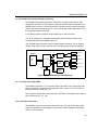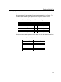
1
TMS320DM368
Evaluation Module
Technical
Reference
2011
DSP Development Systems
TMS320DM368 Evaluation
Module Technical Reference
514565-0001 Rev. B
March 2011
SPECTRUM DIGITAL, INC.
12502 Exchange Drive, Suite 440 Stafford, TX. 77477
Tel: 281.494.4505
Fax: 281.494.5310
[email protected] www.spectrumdigital.com
IMPORTANT NOTICE
Spectrum Digital, Inc. reserves the right to make changes to its products or to discontinue any
product or service without notice. Customers are advised to obtain the latest version of relevant
information to verify that the data being relied on is current before placing orders.
Spectrum Digital, Inc. warrants performance of its products and related software to current
specifications in accordance with Spectrum Digital’s standard warranty. Testing and other quality
control techniques are utilized to the extent deemed necessary to support this warranty.
Please be aware that the products described herein are not intended for use in life-support
appliances, devices, or systems. Spectrum Digital does not warrant nor is Spectrum Digital liable for
the product described herein to be used in other than a development environment.
Spectrum Digital, Inc. assumes no liability for applications assistance, customer product design,
software performance, or infringement of patents or services described herein. Nor does Spectrum
Digital warrant or represent any license, either express or implied, is granted under any patent right,
copyright, or other intellectual property right of Spectrum Digital, Inc. covering or relating to any
combination, machine, or process in which such Digital Signal Processing development products or
services might be or are used.
WARNING
This equipment is intended for use in a laboratory test environment only. It generates, uses, and can
radiate radio frequency energy and has not been tested for compliance with the limits of computing
devices pursuant to subpart J of part 15 of FCC rules, which are designed to provide reasonable
protection against radio frequency interference. Operation of this equipment in other environments
may cause interference with radio communications, in which case the user at his own expense will be
required to take whatever measures necessary to correct this interference.
Copyright © 2011 Spectrum Digital, Inc.
Contents
1
Introduction to the DM368 Evaluation Module . . . . . . . . . . . . . . . . . . . . . . . . . . . . . . . .
Provides you with a description of the DM368 Evaluation Module, key features, and
block diagram.
1.1 Key Features
..........................................................
1.2 Functional Overview of the DM368 EVM
.................................
1.3 Basic Operation . . . . . . . . . . . . . . . . . . . . . . . . . . . . . . . . . . . . . . . . . . . . . . . . . . . . . . . . .
1.4 Memory Map . . . . . . . . . . . . . . . . . . . . . . . . . . . . . . . . . . . . . . . . . . . . . . . . . . . . . . . . . .
1.5 Boot / Configuration Switch Settings
.......................................
1.6 Power Supply
.........................................................
1.7 DM368 User Interface Module with Touch Screen
...........................
1.7.1 DM368 UIM Installation on DM368 EVM Checklist
.........................
1.7.2 Removal of UIM from DM368 EVM Checklist
.............................
2
Board Components . . . . . . . . . . . . . . . . . . . . . . . . . . . . . . . . . . . . . . . . . . . . . . . . . . . . . . . .
Describes the operation of the major board components on the DM368 Evaluation Module.
2.1 EMIF Interfaces . . . . . . . . . . . . . . . . . . . . . . . . . . . . . . . . . . . . . . . . . . . . . . . . . . . . . . . . .
2.1.1 Flash, NAND Flash
....................................................
2.1.1.1 One NAND
.........................................................
2.1.1.2 CPLD Interface
.....................................................
2.1.1.2.1 Register 0, CPLD Version
...........................................
2.1.1.2.2 Register 1, Test Register
............................................
2.1.1.2.3 Register 2, LED Register
............................................
2.1.1.2.4 Register 3, Board Mux Control Register
................................
2.1.1.2.5 Register 4, Board Switch Register
....................................
2.1.1.2.6 Register 5, Power Control Register
...................................
2.1.1.2.7 Register 6, GPIO Video Register
.....................................
2.1.1.2.8 Register 7, Media Card Status
.......................................
2.1.1.2.9 Register 8, DILC Output Pin Mapping
.................................
2.1.1.2.10 Register 9, DILC Input Pin Mapping
.................................
2.1.1.2.11 Register 10, Imager Internal I/O Direction Register 0
...................
2.1.1.2.12 Register 11, Internal I/O Mux Register 0
..............................
2.1.1.2.13 Register 12, Internal I/O Mux Register 1
.............................
2.1.1.2.14 Register 13, Imager Internal I/O Direction Register 1
...................
2.1.1.2.15 Register 14, Imager Internal I/O Mux Register 2
......................
2.1.1.2.16 Register 15, Imager Internal I/O Mux Register 3
.......................
2.1.1.2.17 Register 16, Imager Internal I/O Direction Register 2
....................
2.1.1.2.18 Register 17, Imager Internal I/O Mux Register 4
......................
2.1.1.2.19 Register 18, Imager Internal I/O Mux Register 5
......................
2.1.1.2.20 Imager Multiplexer Mapping
.......................................
2.1.1.2.21 Register 19, Board RESET/EXTCLK Select Register
..................
2.1.1.2.22 Register 20, Interrupt Select Register
..............................
1-1
1-2
1-5
1-5
1-6
1-7
1-8
1-8
1-9
1-10
2-1
2-2
2-2
2-2
2-4
2-6
2-6
2-6
2-6
2-7
2-7
2-8
2-9
2-9
2-10
2-10
2-11
2-11
2-12
2-12
2-13
2-13
2-14
2-14
2-15
2-17
2-18
2.1.1.2.23 Register 720, CCD Internal I/O Direction Register 1
....................
2.1.1.2.24 Register 721, CCS Internal I/O Read/Write Register 1
..................
2.1.1.2.25 Register 722, CCD Internal I/O Direction Register 2
....................
2.1.1.2.26 Register 723, CCD Internal I/O Read/Write Register 2
..................
2.1.1.2.27 Register 724, CCD Internal I/O Direction Register 3
....................
2.1.1.2.28 Register 725, CCD Internal I/O Read/Write Register 3
..................
2.1.1.3 Key Pad Interface
..................................................
2.1.2 DDR2 Memory Interface . . . . . . . . . . . . . . . . . . . . . . . . . . . . . . . . . . . . . . . . . . . . . .
2.1.3 Media Card Interface
..............................................
2.1.4 UART Interface
..................................................
2.1.5 USB Interface
....................................................
2.2 Input Video Port/Imager Input Port Interfaces
...............................
2.2.1 On Chip Video Output DAC
............................................
2.2.2 LCD Video Connectors
...............................................
2.3 AIC3101 Interface
....................................................
2.4 On Chip Voice Codec
...................................................
2.5 On Chip ADC
..........................................................
2.6 On Chip RTC
........................................................
2.7 Ethernet Interface
......................................................
2.8 I2C Interface . . . . . . . . . . . . . . . . . . . . . . . . . . . . . . . . . . . . . . . . . . . . . . . . . . . . . . . . . . .
2.8.1 MSP430 . . . . . . . . . . . . . . . . . . . . . . . . . . . . . . . . . . . . . . . . . . . . . . . . . . . . . . . . . . . .
2.9 Daughter Card Interface
...............................................
2.10 DM368 CPU Video Clocks
............................................
2.11 Battery
.............................................................
3
Physical Specifications . . . . . . . . . . . . . . . . . . . . . . . . . . . . . . . . . . . . . . . . . . . . . . . . . . . .
Describes the physical layout of the DM368 Evaluation Module and its connectors.
3.1 Board Layout
........................................................
3.2 Connectors
........................................................
3.2.1 J1, MiniAB USB Connector and Jumpers
................................
3.2.2 J2, 14 Pin External JTAG Header
........................................
3.2.3 J3, MSP430 JTAG Header
...........................................
3.2.4 J4, Spare Jumper Holder
...............................................
3.2.5 J5, 20 Pin ARM JTAG Emulation Header
..................................
3.2.6 J6, USB Capacitance Select
...........................................
3.2.7 J7, +5 Volts Input
....................................................
3.2.8 J12, SD/MMC/MS Card Interface
.......................................
3.2.9 J10, Imager Interface
................................................
3.2.10 J14, EMIF/UPI DC Interface
.........................................
3.2.11 J8, Y Component Video In, RCA Jack (Green)
..........................
3.2.12 J9, Pb Component Video In, RCA Jack (Blue)
..........................
3.2.13 J11, Pr Component Video In, RCA Jack (Red)
.........................
3.2.14 J15, S-Video In
....................................................
3.2.15 J13, CVBS/Y Input, RCA Jack (Yellow)
................................
3.2.16 J16, Composite TV Out, RCA Jack (Yellow)
............................
3.2.17 J17, Y Component Video Out, RCA Jack (Green)
........................
3.2.18 J20, Pb Component Video Out, RCA Jack (Blue)
........................
3.2.19 J21, Pr Component Video Out, RCA Jack (Red)
.........................
3.2.20 J18, J19, Video Output DC
...........................................
3.2.21 J22, CPLD Programming Header
.....................................
2-18
2-19
2-19
2-20
2-20
2-21
2-21
2-22
2-22
2-22
2-22
2-23
2-23
2-23
2-24
2-25
2-25
2-25
2-26
2-26
2-27
2-27
2-27
2-28
3-1
3-3
3-5
3-6
3-7
3-8
3-8
3-9
3-9
3-10
3-10
3-11
3-12
3-13
3-13
3-14
3-14
3-15
3-15
3-16
3-16
3-17
3-18
3-19
3.2.22 J23, I/O Interface Header
............................................
3.2.23 J24, DILC Host Connector
...........................................
3.2.24 J25, MMC/SD Connector
............................................
3.2.26 P1, RS-232 UART
..................................................
3.2.27 P2, Ethernet Interface
...............................................
3.2.28 P3, Microphone In
..................................................
3.2.29 P4, Line In
........................................................
3.2.30 P5, Line Out
.......................................................
3.2.31 P6, Headphone Out
.................................................
3.2.32 U1, Infrared Interface
...............................................
3.2.33 SPK1, Speaker Interface
.............................................
3.2.34 BHT1, Battery Interface
.............................................
3.2.35 M1, Microphone Interface
............................................
3.3 LEDs
................................................................
3.4 Switches
.............................................................
3.4.1 SW1, EMU0/1 Select Switch
...........................................
3.4.2 SW2, PWCTRO0 Pushbutton
.........................................
3.4.3 SW3, RESET Pushbutton
............................................
3.4.4 SW4, Boot Mode / Configuration Select
..................................
3.4.5 SW5, Board Configuration Select
......................................
3.4.6 SW6 - SW21, Function Pushbuttons
....................................
3.4.7 SW22, MSP430 IO0 Pushbutton
.......................................
3.4.8 SW23, PRTSC Mode Select
..........................................
3.5 Jumpers
............................................................
3.5.1 JP1, Jumper Block
..................................................
3.5.2 JP2, Unpopulated Jumper
............................................
3.5.3 JP28, Unpopulated Jumper
...........................................
3.5.4 J26, USB ID Select
..................................................
3.5.5 J27, U14 LL8 Voltage Select
..........................................
3.6 Test Points
........................................................
A Schematics
..............................................................
Contains the schematics for the DM368 Evaluation Module
B Mechanical Information
..................................................
Contains the mechanical information about the DM368 Evaluation Module
3-19
3-20
3-21
3-22
3-23
3-24
3-24
3-25
3-25
3-26
3-26
3-27
3-27
3-28
3-29
3-30
3-30
3-30
3-31
3-32
3-32
3-33
3-33
3-34
3-34
3-34
3-34
3-34
3-34
3-35
A-1
B-1
About This Manual
This document describes the board level operations of the DM368 Evaluation Module
(EVM). The EVM is based on the Texas Instruments TMS320DM368 Processor.
The DM368 Evaluation Module is a table top card that allows engineers and software
developers to evaluate certain characteristics of the DM368 processor to determine if
the processor meets the designers application requirements. Evaluators can create
software to execute on board or expand the system in a variety of ways.
Notational Conventions
This document uses the following conventions.
The DM368 Evaluation Module will sometimes be referred to as the DM368 EVM or
EVM.
Program listings, program examples, and interactive displays are shown in a special
italic typeface. Here is a sample program listing.
equations
!rd = !strobe&rw;
Information About Cautions
This book may contain cautions.
This is an example of a caution statement.
A caution statement describes a situation that could potentially damage your software,
or hardware, or other equipment. The information in a caution is provided for your
protection. Please read each caution carefully.
Related Documents, Application Notes and User Guides
Information regarding the TMS320DM368 can be found at the following Texas
Instruments website:
http://www.ti.com
Table 1: Manual History
Revision
History
A
Beta Release
B
Edits to CPLD registers, Tables
Table 2: Board History
PWB
Revision
A
History
Beta Release
Chapter 1
Introduction to the
DM368 EVM
Chapter One provides a description of the DM368 EVM along with the key
features and a block diagram of the circuit board.
Topic
1.1
1.2
1.3
1.4
1.5
1.6
1.7
1.7.1
1.7.2
Page
Key Features
Functional Overview of the DM368 EVM
Basic Operation
Memory Map
Boot / Configuration Switch Settings
Power Supply
DM368 User Interface Module with Touch Screen
DM368 UIM Installation on DM368 EVM Checklist
Removal of UIM from the DM368 EVM Checklist
1-2
1-5
1-5
1-6
1-7
1-8
1-8
1-9
1-10
1-1
Spectrum Digital, Inc
1.1 Key Features
USB
JTAG (14)
1 2
RS-232
SW1
The DM368 EVM is a standalone development platform that enables users to
evaluate and develop applications for the TMS320DM368 processor. Schematics,
logic equations and application notes are available to ease hardware development and
reduce time to market.
MSP430
JTAG
ENET
RJ45
JTAG (20)
IR
MIC
PWR
MIC IN
MSP430
KSZ8001
PHY
Battery
PRTSCC On
McBSP
1 2
LINE OUT
SW23
JTAG
SPI
ROM
TPS65530
Power
MII
SPI0
MUX
HD Video In Connector
USB
UART0
SD/MMC
SD/MMC
SD0 on Top
SD1 on Bottom
DDR2
16
DM368
Video In
DAC Out
HD Video
Decoder
TVP7002
SD Video
Decoder
TVP5146
Y
Pb/Cb
Pr/Cr
Comp
SW4
1
2
3
4
5
6
1
2
3
4
5
6
EMIF
I2C
ROM
SW5
S-Video
THS7303
J14 - EMIF
HP OUT
I2C Bus
THS7353
Reset
One
NAND
LINE IN
AIC
3101
Comp
NAND
Y
LEDs
CPLD
Pb/Cb
Pr/Cr
J19
J18
Digital
Video Out
Speaker
LCD Interface
J23
Keypad
Camera IF
Figure 1-1, Block Diagram DM368 EVM
The EVM comes with a full complement of on board devices that suit a wide variety of
application environments. Key features include:
• A Texas Instruments DM368 processor with an ARM9 processor operating up to
432 MHz.
• Compatible with DM368 User Interface Module (UIM) with touch screen. The UIM
has a 4.3” color LCD with 480 x 272 pixels.
• 1 video input port, supports composite or S video (NTSC or PAL formats)
• 1 set of 3 component video inputs supports capture up to 720P 60 FPS/1080P
30 FPS resolution
• 1 composite video DAC output (NTSC or PAL formats)
• 1 set of 3 component video DACs supports resolution up to 720P resolution
• 128 Mbytes of 400 MHz DDR2 DRAM
1-2
DM368 EVM Technical Reference
Spectrum Digital, Inc
• UART Interface
• SD/MMC/MS, MMC/SD Media Card Interfaces
• 2 Gigabytes NAND Flash
• 128 Megabytes of One NAND
• AIC3101 stereo codec
• USB2 Interface
• 10/100 MBS RMII Ethernet Interface
• SPI EEPROM
• IR Remote Interface via MSP430
• Configurable boot load options
• 8 user LEDs/16 user push button switches
• Single voltage power supply (+5V)
• Expansion connectors for daughter card use
• 14 Pin TI JTAG/20 Pin ARM JTAG Interfaces
1-3
Spectrum Digital, Inc
The two figures below show the DM368 EVM without the display and with the display
mounted.
Figure 1-2, DM368 EVM Without DM368 UIM
Figure 1-3, DM368 EVM With DM368 UIM
1-4
DM368 EVM Technical Reference
Spectrum Digital, Inc
1.2 Functional Overview of the DM368 EVM
The DM368 on the EVM interfaces to on-board peripherals through the 8/16-bit wide
Async EMIF peripheral interface pins. The DDR2 memory is connected to its own
dedicated 16 bit wide bus. The Async EMIF bus is also connected to the NAND and
One NAND flash.
On board video decoders and on chip encoders interface video streams to the DM368
processor. One composite channel and one set of 3 component channel
encoder/decoder are standard on the EVM. On screen display functions are
implemented in software on the DM368 processor.
An on-board AIC3101 codec allows the DSP to transmit and receive analog audio
signals. The I2C bus is used for the codec control interface, while the McBSP controls
the audio stream. Signal interfacing is done through 3.5mm audio jacks that correspond
to microphone input, headphone output, line input, and line output.
The EVM includes 8 user LEDs, 16 user push button switches, and an IR interface
which provide the user with application interaction.
An included +5V external power supply is used to power the board. On-board switching
voltage regulators provide the +1.2 to 1.35V CPU core voltage, +3.3V for peripherals
and +1.8V for DDR2 memory.
The DM368 EVM has a 10/100 ethernet interface which provides a standard high
speed link to other devices.
The on board media card interface allows the user to conveniently load/store data from
a variety of standard memory card formats. An on-chip Real Time Clock is integrated
into the DM368 for time based applications.
1.3 Basic Operation
The EVM is designed to work with TI’s Code Composer Studio IDETM, or standard GDB
tool environments. Code Composer communicates with the board through an external
JTAG emulator.
1-5
Spectrum Digital, Inc
1.4 Memory Map
The DM368 processor has a byte addressable address space. There are some
limitations to byte addressing which are determined by peripheral interconnection to the
DM368 device. Program code and data can be placed anywhere in the unified address
space. Addresses are multiple sizes depending on hardware implementation. Refer to
the appropriate device data sheets for more details.
The memory map shows the address space of a generic DM368 processor on the left
with specific details of how each region is used on the right. By default, the internal
memory sits at the beginning of the address space. Portions of memory can be
remapped in software as L2 cache rather than fixed RAM.
The part incorporates a dual EMIF interface. One dedicated EMIF directly interfaces to
the DDR2 memory. The other EMIF has 2 separate addressable regions called chip
enable spaces (CE0 & CE1). The NAND Flash, one NAND, and CPLD are mapped into
these chip enable spaces.
DM368 EVM
Address
0x00000000
Memory Map Address Space
ARM Instruction RAM
0x00007FFF
0x00008000
ARM Instruction ROM
0x0000BFFF
0x00010000
ARM RAM (Data)
0x00017FFF
0x01C00000
CFG Bus Peripherals
0x01FFFFFF
0x02000000
CE0 - ASYNC EMIF (Data)
0x03FFFFFF
0x04000000
CE1
0x05FFFFFF
0x20000000
DDR EMIF Control Regs
0x2007FFFF
0x80000000
DDR EMIF
0x87FFFFFF
0x88000000
0x8FFFFFFF
DDR Expansion
(reserved)
Figure 1-4, Memory Map, DM368 EVM
1-6
DM368 EVM Technical Reference
Spectrum Digital, Inc
Shown below is a break out of the memory spaces.
Memory Space
Address
0x02000000
NAND Chip Select 0 / One NAND
0x02004000
NAND Chip Select 1
0x40000000
CPLD Control Registers
Figure 1-5, DM368 EVM Chip Enable Memory Space
1.5 Boot / Configuration Switch Settings
The EVM has a configuration switch that allow users to control the Boot and EMIF
configuration state of the processor when it is released from reset. The switch SW4
determines the source for processor booting. By default the switches are configured to
NAND Flash boot. The EMIF configuration switch must be set accordingly. This switch
configures the DM368 pin muxing at RESET. The default for the pin muxing is shown
below. For additional pin muxing requirements please refer to the D368 data sheet.
Table 1: SW4, ARM Boot Mode Select
Pos 3
Pos 2
Pos 1
HW Code
Boot Mode
ON
ON
ON
000
NAND Boot *
ON
ON
OFF
001
ASYNC EMIF
ON
OFF
ON
010
MMC/SD Boot
ON
OFF
OFF
011
UART Boot
OFF
ON
ON
100
USB Boot
OFF
ON
OFF
101
SPI Boot
OFF
OFF
ON
110
EMAC Boot
OFF
OFF
OFF
111
HPI Boot
Table 2: SW4, ARM EMIF Configuration Mode Select
Pos 6
Pos 5
Pos 4
HW Code
Configuration Mode
ON
ON
ON
000
8-bit AEMIF Configuration *
ON
ON
OFF
001
16-bit AEMIF Configuration
* default setting
1-7
Spectrum Digital, Inc
1.6 Power Supply
The EVM operates from a single +5V external power supply connected to the main
power input (J7), a 2.5 MM. barrel-type plug. Internally, the +5V input is converted
into +1.2 to 1.35V, +1.8V and +3.3V using Texas Instruments TPS65530 power
management IC and various linear regulators. The +1.2 to 1.35V supply is used for the
DSP core while the +3.3V supply is used for the DSP's I/O buffers and other chips on
the board. The +1.8 volt supply is used for DM368 DDR2 memory, and other on chip
peripherals.
1.7 DM368 User Interface Module with Touch Screen
The DM368 EVM can be used with the DM368 User Interface Module (UIM) with touch
screen. The DM368 UIM plugs on the DM368 EVM and is shown in figure 1-3 above.
The table below shows the mating of the connectors on the DM368 EVM to the
connectors on the DM368 UIM.
Table 3: DM368 - Mating UIM Connectors
1-8
DM368
Connector
Mating UIM
Connectors
J18
J2
J19
J1
J23
J6
DM368 EVM Technical Reference
Spectrum Digital, Inc
1.7.1 DM368 UIM Installation on DM368 EVM Checklist
To install the DM368 UIM on the DM368 EVM execute the following checklist:
o Turn off the power to your DM368 EVM !
o Align connectors J1, J2, and J6 of the UIM with connectors J18, J19,and J23 on
the DM368 EVM.
J2 to J18
J1 to J19
J6 to J23
Figure 1-6, Align UIM and DM368 EVM Connectors
o Visually inspect the alignment of the connectors from the card edge (Spectrum
Digital logo) to insure all 6 connectors are mated together.
o Carefully push the UIM down onto the DM368 EVM.
o Turn on the power to your DM368 EVM and verify operation.
1-9
Spectrum Digital, Inc
1.7.2 Removal of UIM from the DM368 EVM Checklist
To remove the UIM from the DM368 EVM execute the following checklist:
o Turn off the power to your DM368 EVM !
o Carefully lift the edges of the UIM circuit board up. If necessary rotate lifting from
right side, bottom edge, left side, right side, .... until the UIM is free from the DM368
EVM.
left
bottom
right
Figure 1-7, Removal of UIM from DM368 EVM
o Safely store the UIM in an anti-static bag.
o Turn on the power to your DM368 EVM and verify operation.
1-10
DM368 EVM Technical Reference
Chapter 2
Board Components
This chapter describes the operation of the major board components on
the DM368 EVM.
Topic
2.1
Asychronous EMIF Interface
2.1.1 NAND Flash
2.1.1.1 One NAND
2.1.1.2 CPLD Interface
2.1.1.2.1 Register 0, CPLD Version
2.1.1.2.2 Register 1, Test Register
2.1.1.2.3 Register 2, LED Register
2.1.1.2.4 Register 3, Board Mux Control Register
2.1.1.2.5 Register 4, Board Switch Register
2.1.1.2.6 Register 5, Power Control Register
2.1.1.2.7 Register 6, GPIO Video Register
2.1.1.2.8 Register 7, Media Card Status
2.1.1.2.9 Register 8, DILC Output Pin Mapping
2.1.1.2.10 Register 9, DILC Input Pin Mapping
2.1.1.2.11 Register 10, Imager Internal I/O Direction Register 0
2.1.1.2.12 Register 11, Internal I/O Mux Register 0
2.1.1.2.13 Register 12, Internal I/O Mux Register 1
2.1.1.2.14 Register 13, Imager Internal I/O Direction Register 1
2.1.1.2.15 Register 14, Imager Internal I/O Mux Register 2
2.1.1.2.16 Register 15, Imager Internal I/O Mux Register 3
2.1.1.2.17 Register 16, Imager Internal I/O Direction Register 2
2.1.1.2.18 Register 17, Imager Internal I/O Mux Register 4
2.1.1.2.19 Register 18, Imager Internal I/O Mux Register 5
2.1.1.2.20 Imager Multiplexer Mapping
2.1.1.2.21 Register 19, Board RESET/EXTCLK Select Register
2.1.1.2.22 Register 20, Interrupt Select Register
2.1.1.2.23 Register 720, CCD Internal I/O Direction Register 1
2.1.1.2.24 Register 721, CCS Internal I/O Read/Write Register 1
2.1.1.2.25 Register 722, CCD Internal I/O Direction Register 2
2.1.1.2.26 Register 723, CCD Internal I/O Read/Write Register 2
2.1.1.2.27 Register 724, CCD Internal I/O Direction Register 3
2.1.1.2.28 Register 725, CCD Internal I/O Read/Write Register 3
Page
2-2
2-2
2-2
2-4
2-6
2-6
2-6
2-6
2-7
2-7
2-8
2-9
2-9
2-10
2-10
2-11
2-11
2-12
2-12
2-13
2-13
2-14
2-14
2-15
2-17
2-18
2-18
2-19
2-19
2-20
2-20
2-21
2-1
Spectrum Digital, Inc
Topic
2.1.1.3
2.1.2
2.1.3
2.1.4
2.1.5
2.2
2.2.1
2.2.2
2.3
2.4
2.5
2.6
2.7
2.8
2.8.1
2.9
2.10
2.11
2-2
Key Pad Interface
DDR2 Memory Interface
Media Card Interface
UART Interface
USB Interface
Input Video Port/Imager Input Port Interfaces
On Chip Video Output DAC
LCD Video Connectors
AIC3101 Interface
On Chip Voice Codec
On Chip ADC
On Chip RTC
Ethernet Interface
I2C Interface
MSP430
Daughter Card Interface
DM368 CPU/Video Clocks
Battery
Page
2-21
2-22
2-22
2-22
2-22
2-23
2-23
2-23
2-24
2-25
2-25
2-25
2-26
2-26
2-27
2-27
2-27
2-28
DM368 EVM Technical Reference
Spectrum Digital, Inc
2.1 Asynchronous EMIF Interface
An asynchronous 16 bit EMIF with two chip enables divide up the address space and
allow for asynchronous accesses on the EVM. This interface connects to the NAND,
One NAND, and CPLD registers on the EVM board.
2.1.1 NAND Flash
The DM368 has 2 gigabytes of NAND Flash memory mapped into the CE0 space. The
NAND Flash memory is used primarily for boot loading and file system on the DM368
EVM. The CE0 selects the device and needs to be configured to 8 bits wide when
accessing the NAND.
Switch SW5, position 1 (OFF) selects CE0 mapped to NAND. The NAND and One
NAND interface share the same CE0 chip select so only 1 device can be operational at
any given time.
When the NAND flash interface is selected the spare address lines can be used by the
internal DM368 key pad interface. This interface is enabled by setting a control bit in
the CPLD to enable the on board CBTLV switches to the keypad matrix.
2.1.1.1 One NAND
The EVM supports 128 Megabytes of One NAND. This interface is 16 bits wide and
CE0 must be configured for 16 bit wide operation when using One NAND. Switch SW5,
position 1 (ON) selects the One NAND device. When the One NAND is selected the on
board NAND is not available. Since the One NAND uses all the asynchronous
EMIF address lines the on-chip key pad controller on the DM368 cannot be used when
the One NAND is selected.
2-3
Spectrum Digital, Inc
2.1.1.2 CPLD Interface
The DM368 incorporates an Altera EPM2210, 256 Ball Grid Array (BGA) CPLD. The
CPLD incorporates a number of internal registers, glue logic, and I/O multiplexing to
allow for a very flexible development platform. The CPLD is accessed via EMIF CE1.
The interface is 8 bits wide. All registers show up as 4 mirror images in the memory
window due to 32 bit addressing and 8 bit data mapping, that is BA0 and BA1 are not
used in the memory decoder for registers.
Address lines A7-A3, A0, BA0, and BA1 are not used in the decoder so that these lines
can be used by the keypad decoder.
The base address of CE1 is 0x0400 0000. Each additional register is accessed on an
increment of 0x0000 0008. The addresses are in the following format:
A13, A12, A11, A10, A9, A8, Ax, Ax, Ax, Ax, Ax, A2, A1, Ax, Ax.
2-4
DM368 EVM Technical Reference
Spectrum Digital, Inc
The following sections describe the registers and their function. A list of the registers is
shown in the table below.
Table 1: CPLD Registers
Reg #
Entire
Address
Address
A13-A8
Address
A2-A1
Function
R/W
0
0x0400 0000
000000
00
CPLD Version
R
1
0x0400 0008
000000
01
Test Register
R,W
2
0x0400 0010
000000
10
LED Register
R,W
3
0x0400 0018
000000
11
Board Mux Control
R,W
4
0x0400 0400
000001
00
Board Switch Register
R
5
0x0400 0408
000001
01
Power Control Register
R,W
6
0x0400 0410
000001
10
GPIO Video Register
R,W
7
0x0400 0418
000001
11
Media Card Status
R
8
0x0400 0800
000010
00
DILC Output Pin Mapping
R,W
9
0x0400 0808
000010
01
DILC Input Pin Mapping
R
10
0x0400 0810
000010
10
Imager Internal I/O Direction Register 0
R,W
11
0x0400 0818
000010
11
Imager Internal I/O Mux Register 0
R,W
12
0x0400 0A00
000011
00
Imager Internal I/O Mux Register 1
R,W
13
0x0400 0A08
000011
01
Imager Internal I/O Direction Register 1
R,W
14
0x0400 0A10
000011
10
Imager Internal I/O Mux Register 2
R,W
15
0x0400 0A18
000011
11
Imager Internal I/O Mux Register 3
R,W
16
0x0400 1000
000100
00
Imager Internal I/O Direction Register 2
R,W
17
0x0400 1008
000100
01
Imager Internal I/O Mux Register 4
R,W
18
0x0400 1010
000100
10
Imager Internal I/O Mux Register 5
R,W
19
0x0400 1018
000100
11
Board RESET Register
R,W
720
0x0400 F800
111110
00
CCD Internal I/O Direction Register 1
R,W
721
0x0400 F808
111110
01
CCD Internal I/O Read/Write Register 1
R,W
722
0x0400 F810
111110
10
CCD Internal I/O Direction Register 2
R,W
723
0x0400 F818
111110
11
CCD Internal I/O Read/Write Register 2
R,W
724
0x0400 FC00 1 1 1 1 1 1
00
CCD Internal I/O Direction Register 3
R,W
725
0x0400 FC08 1 1 1 1 1 1
01
CCD Internal I/O Read/Write Register 3
R,W
2-5
Spectrum Digital, Inc
2.1.1.2.1 Register 0, CPLD Version
This read only, 8 bit register, contains the 4 bit board type and the 4 bit CPLD version
for version control. The default value is 0x21 for the DM368 EVM.
2.1.1.2.2 Register 1, Test Register
This read only, 8 bit register, has a default value of 0xA5 and can be read and written to
test the memory interface.
2.1.1.2.3 Register 2, LED Register
This 8 bit, read/write register controls the user LEDs. A data bit of ‘0’ in each bit
location turns on an LED. Similarly a ‘1’ turns off the LED in each bit position.
2.1.1.2.4 Register 3, Board Mux Control Register
This 8 bit, read/write control register (default = 0x00) controls keypad, AIC, SD,
Ethernet, and Video In multiplexers as shown in the table below.
Table 2: Register 3, Board Mux Control Register
2-6
Bit #
Signal
7
EMIF_KEYPAD_CTL
6
SEL_SD1_GPIO_CTL
5
SEL_AICn_GPIO_CTL
4
Advanced LCD/Touch control
3
SEL_ENET_GPIO_CTL
2
DECODER_IMAGER_S2_CTL
1
DECODER_IMAGER_S1_CTL
0
DECODER_IMAGER_S0_CTL
State
Function
0
Addresses on Muxes (ONE NAND Mode)
1
Addresses are available for keypad
0
Enables SD card slot 1
1
Signals for SD1 card slot 1 go to CPLD
imager GPIO
0
Enables McBSP signals to AIC3101 codec
1
McBSP signals go to CPLD for imager GPIO
0/1
0 = normal mode,
1 = advanced mode for Avnet LCD panel
0
Enable Ethernet signals to PHY
1
Ethernet signals go to CPLD for imager GPIO
S[2:0]
0 0 1 = Selects TVP7002 as input to DM368
video input port
0 1 0 = Selects imager as input to DM368
video input port
1 0 1 = Selects TVP5146 as input to DM368
video input port
DM368 EVM Technical Reference
Spectrum Digital, Inc
2.1.1.2.5 Register 4, Board Switch Register
This 8 bit, read only register mirrors the values set on switch SW5. These signals are
shown in the table below.
Table 3: Register 4, Board Switch Register
Bit #
SW5 Position
Signal
7
Reserved
N/A
6
Reserved
N/A
5
1
SEL_NAND_LOW
0 = NAND mapped to CE0,
1 = ONE NAND mapped to CE0
4
2
SEL_EXTRA1
3
3
SEL_EXTRA2
2
4
SEL_EXTRA3
1
5
CPU_VSEL1
0 = Vcore at 1.2V
1 = Vcore at 1.35 V
0
6
SEL_NTAS_MODE
2.1.1.2.6 Register 5, Power Control Register
Register 5 is a 8 bit, read/write register that controls on board voltage regulator
functions. The default data value is 0b00000000. These controls are shown in the table
below.
Table 4: Register 5, Power Control Register
Bit #
Signal
Function
7
LCD_OE_5V
0,1 = Sets U32 FDC6331L Pin to 0,1
ENABLE_LCD_3V3
0 = Disables U31 TPS74701
1 = Enables U31 TPS74701
6
5
Reserved
4
EN7
0,1 = Sets U14 TPS65530 EN7 pin to 0,1
3
ENAFE
0,1 = Sets U14 TPS65530 ENAFE pin to 0,1
2
SEQ56
0,1 = Sets U14 TPS65530 SEQ56 pin to 0,1
1
EN56
0,1 = Sets U14 TPS65530 EN56 pin to 0,1
0
ENABLE_LCD_15V
0 = Disables U34 TPS61080 register
0 = Enables U34 TPS61080 register
2-7
Spectrum Digital, Inc
2.1.1.2.7 Register 6, GPIO Video Register
Register 6 is a 8 bit, read/write register that controls the mapping of GPIO30/32/33,
VDIN_WE, DRV_BUS. The default data value is 0b00000000. These controls are
shown in the table below.
Table 5: Register 6, GPIO Video Register
Bit #
Signal
Function
7
Reserved
6
Reserved
5
C_FIELD
1 = DM368 Ball E13 mapped to
EXP CONN CCD_FIELD
4
C_WE
1 = DM368 Ball E13 mapped to
EXP CONN CCD_WEN
3
24 BIT COLOR
1 = Map GPIO30,32,33 to
G1,R0,R1 on LCD EXP CONNS
2
C_WE_FLD_VBUS_DRV
1 = DM368 BALL E13 Drives U4, TPS2065
1
GIO33_VBUS_DRV
1 = GIO33 drives U4, TPS2065
0
VBUS_DRV_ALT
1 = Drives VBUS ENABLE to U4, TPS2065
ENABLE VBUS_DRV (U4, TPS2065) will = 1 when any of the following occur:
- When SW5-2 (SEL_EXTRA1_ = 1 for test
- When VBUS_DRV_ALT = 1
ENABLE VBUS_DRV (U4, TPS2065) will = DM368 GIO33 when
GIO33_VBUS_DRV = 1
ENABLE VBUS_DRV (U4, TPS2065) will = DM368 Ball E13 when
C_WE_FLD_VBUS_DRV = 1
2-8
DM368 EVM Technical Reference
Spectrum Digital, Inc
2.1.1.2.8 Register 7, Media Card Status
Register 7 is a 8 bit, read only register that reads the “Insert” and “Write Protect” status
of media cards. These functions of these bits are shown in the table below.
Table 6: Register 7, Media Card Status
Bit #
Signal
Function
7
Reserved
Reads 0
6
Reserved
Reads 0
5
SD_MMC_1 WRITE PROTECT
0 = Write Protect
4
SD_MMC_1 INSERT
0 = Insert
3
Reserved
Reads 0
2
SD_MMC0 MS INSERT
0 = Insert
1
SD_MMC_0 WRITE PROTECT
0 = Write Protect
0
SD_MMC_0 INSERT
0 = Insert
2.1.1.2.9 Register 8, DILC Output Pin Mapping
Register 8 is a 8 bit, read/write register that maps DM368 GPIO and SPI2 pins to the
DILC connector. The default data value is 0b11111111. The mapping of these pins is
shown in the table below.
Table 7: Register 8, DILC Output Pin Mapping
Bit #
Signal
Function
7
DILC_DRV_VBUS
Register drives DILC DRV_VBUS pin
when bit 6 = 0
6
DILC_DRV_VBUS_IO
0 = Internal register bit 7 drives DILC pin
5
DILC_VBUS_DET_DRV
Register drives DILC pin VBUS_DET
when bit 4 = 0
4
DILC_VBUS_DET_IO
0 = Internal register bit 5 drives DILC pin
3
Reserved
N/A
2
CPU_GPIO32_IO
0 = IN, SPI2_DILC drives GIO32
1 = OUT, GIO32 drives SPI2_DILC
1
CPU_GPIO31_IO
0 = IN, SPI2_DILC drives GIO31
1 = OUT, GIO31 drives SPI2_DILC
0
CPU_GPIO30_IO
0 = IN, SPI2_DILC drives GIO30
1 = OUT, GIO30 drives SPI2_DILC
2-9
Spectrum Digital, Inc
2.1.1.2.10 Register 9, DILC Input Pin Mapping
Register 9 is a 8 bit, read only register that maps DILC pins to read contents on this
register. The mapping of these pins is shown in the table below.
Table 8: Register 9, DILC Input Pin Mapping
Bit #
Function
7
Reserved
6
Reads value of DILC connector pin GIO_DILC_DRV_VBUS1
5
Reads value of DILC connector pin GIO_DILC_DRV_DET
4
Reserved
3
Reads value of DILC connector pin GIO_DILC_DOCK_DET
2
Reads value of DILC connector pin GIO_DILC_CAM_PWR_DECT
1
Reads value of DILC connector pin GIO_DILC_AVJ_DET
0
Reads value of DILC connector pin GIO_DILC_CHG_CTL
2.1.1.2.11 Register 10, Imager Internal I/O Direction Register 0
Register 10 is a 8 bit, read/write register that controls DM368 GPIO to IMAGER
connector pin input/output mapping. The default data value is 0b11111111. This
mapping is shown in the table below.
Table 9: Register 10, Imager Internal I/O Direction Register 0
2-10
Bit #
Function
Mapping
7
0 = GPIO_MD8 to DM368 pin
0 = Outputs
1 = DM368 pins are inputs
6
0 = GPIO_MD7 to DM368 pin
0 = Outputs
1 = DM368 pins are inputs
5
0 = GPIO_MD6 to DM368 pin
0 = Outputs
1 = DM368 pins are inputs
4
0 = GPIO_MD5 to DM368 pin
0 = Outputs
1 = DM368 pins are inputs
3
0 = GPIO_MD4 to DM368 pin
0 = Outputs
1 = DM368 pins are inputs
2
0 = GPIO_MD3 to DM368 pin
0 = Outputs
1 = DM368 pins are inputs
1
0 = SPI4_SDI_GPIO_MD2 to DM368 pin
0 = Outputs
1 = DM368 pins are inputs
0
0 = GPIO_MD1 to DM368 pin
0 = Outputs
1 = DM368 pins are inputs
DM368 EVM Technical Reference
Spectrum Digital, Inc
2.1.1.2.12 Register 11, Internal I/O Mux Register 0
Register 11 is a 8 bit, read/write register that controls DM368 GPIO Muxing to IMAGER
connector pin input. The default data is 0b00000000. The table below shows this
muxing.
Table 10: Register 11, Internal I/O Mux Register 0
Bit #
Muxing
7
0 = GPIO_MD4 MUX SELB
6
0 = GPIO_MD4 MUX SELA
5
0 = GPIO_MD3 MUX SELB
4
0 = GPIO_MD3 MUX SELA
3
0 = SPI4_SDI_GPIO_MD2 MUX SELB
2
0 = SPI4_SDI_GPIO_MD2 MUX SELA
1
0 = GPIO_MD1 MUX SELB
0
0 = GPIO_MD1 MUX SELA
2.1.1.2.13 Register 12, Internal I/O Mux Register 1
Register 12 is a 8 bit, read/write register that controls DM368 GPIO Muxing to IMAGER
connector pin input. The default data is 0b00000000. The table below shows this
muxing.
Table 11: Register 12, Internal I/O Mux Register 1
Bit #
Muxing
7
0 = GPIO_MD8 MUX SELB
6
0 = GPIO_MD8 MUX SELA
5
0 = GPIO_MD7 MUX SELB
4
0 = GPIO_MD7 MUX SELA
3
0 = GPIO_MD6 MUX SELB
2
0 = GPIO_MD6 MUX SELA
1
0 = GPIO_MD5 MUX SELB
0
0 = GPIO_MD5 MUX SELA
2-11
Spectrum Digital, Inc
2.1.1.2.14 Register 13, Imager Internal I/O Direction Register 1
Register 13 is a 8 bit, read/write register that controls DM368 GPIO to IMAGER
connector pin input/output mapping. The default data is 0b00000000. This mapping is
shown in the table below.
Table 12: Register 13, Imager Internal I/O Direction Register 1
Bit #
Function
Mapping
7
0 = GPIO_MD16 to DM368 pin
0 = Outputs
1 = DM368 pins are inputs
6
0 = GPIO_MD15 to DM368 pin
0 = Outputs
1 = DM368 pins are inputs
5
0 = GPIO_MD14 to DM368 pin
0 = Outputs
1 = DM368 pins are inputs
4
0 = GPIO_MD13 to DM368 pin
0 = Outputs
1 = DM368 pins are inputs
3
0 = GPIO_MD12 to DM368 pin
0 = Outputs
1 = DM368 pins are inputs
2
0 = GPIO_MD11 to DM368 pin
0 = Outputs
1 = DM368 pins are inputs
1
0 = GPIO_MD10 to DM368 pin
0 = Outputs
1 = DM368 pins are inputs
0
0 = GPIO_MD9 to DM368 pin
0 = Outputs
1 = DM368 pins are inputs
2.1.1.2.15 Register 14, Imager Internal I/O Mux Register 2
Register 14 is a 8 bit, read/write register that controls DM368 GPIO Muxing to IMAGER
connector pin input. The default data is 0b00000000. The table below shows this
muxing.
Table 13: Register 12, Imager Internal I/O Mux Register 2
2-12
Bit #
Muxing
7
0 = GPIO_MD12 MUX SELB
6
0 = GPIO_MD12 MUX SELA
5
0 = GPIO_MD11 MUX SELB
4
0 = GPIO_MD11 MUX SELA
3
0 = GPIO_MD10 MUX SELB
2
0 = GPIO_MD10 MUX SELA
1
0 = GPIO_MD9 MUX SELB
0
0 = GPIO_MD9 MUX SELA
DM368 EVM Technical Reference
Spectrum Digital, Inc
2.1.1.2.16 Register 15, Imager Internal I/O Mux Register 3
Register 14 is a 8 bit, read/write register that controls DM368 GPIO Muxing to IMAGER
connector pin input. The default data is 0b00000000. The table below shows this
muxing.
Table 14: Register 15, Imager Internal I/O Mux Register 3
Bit #
Muxing
7
0 = GPIO_MD16 MUX SELB
6
0 = GPIO_MD16 MUX SELA
5
0 = GPIO_MD15 MUX SELB
4
0 = GPIO_MD15 MUX SELA
3
0 = GPIO_MD14 MUX SELB
2
0 = GPIO_MD14 MUX SELA
1
0 = GPIO_MD13 MUX SELB
0
0 = GPIO_MD13 MUX SELA
2.1.1.2.17 Register 16, Imager Internal I/O Direction Register 3
Register 16 is a 8 bit, read/write register that controls DM368 GPIO to IMAGER
connector pin input/output mapping. The default data is 0b00000000. This mapping is
shown in the table below.
Table 15: Register 16, Imager Internal I/O Direction Register 3
Bit #
Function
Mapping
7
Reserved
6
0 = CCD_DDS_RST to DM368 pin
0 = Outputs
1 = DM368 pins are inputs
5
0 = PWM_CCD_SUB to DM368 pin
0 = Outputs
1 = DM368 pins are inputs
4
0 = GPIO_TACH to DM368 pin
0 = Outputs
1 = DM368 pins are inputs
3
0 = GPIO_MST_SLV to DM368 pin
0 = Outputs
1 = DM368 pins are inputs
2
0 = GPIO_MD19 to DM368 pin
0 = Outputs
1 = DM368 pins are inputs
1
0 = GPIO_MD18 to DM368 pin
0 = Outputs
1 = DM368 pins are inputs
0
0 = GPIO_MD17 to DM368 pin
0 = Outputs
1 = DM368 pins are inputs
2-13
Spectrum Digital, Inc
2.1.1.2.18 Register 17, Imager Internal I/O Mux Register 4
Register 17 is a 8 bit, read/write register that controls DM368 GPIO Muxing to IMAGER
connector pin input. The default data is 0b00000000. The table below shows this
muxing.
Table 16: Register 17, Imager Internal I/O Mux Register 4
Bit #
Muxing
7
0 = GPIO__MST_SLV MUX SELB
6
0 = GPIO__MST_SLV MUX SELA
5
0 = GPIO_MD19 MUX SELB
4
0 = GPIO_MD19 MUX SELA
3
0 = GPIO_MD18 MUX SELB
2
0 = GPIO_MD18 MUX SELA
1
0 = GPIO_MD17 MUX SELB
0
0 = GPIO_MD17 MUX SELA
2.1.1.2.19 Register 18, Imager Internal I/O Mux Register 5
Register 18 is a 8 bit, read/write register that controls DM368 GPIO Muxing to IMAGER
connector pin input. The default data is 0b00000000. The table below shows this
muxing.
Table 17: Register 17, Imager Internal I/O Mux Register 5
2-14
Bit #
Muxing
7
Reserved
6
Reserved
5
0 = CCD_DDS_RST MUX SELB
4
0 = CCD_DDS_RST MUX SELA
3
0 = PWM_CCD_SUB MUX SELB
2
0 = PWM_CCD_SUB MUX SELA
1
0 = GPIO_TACH MUX SELB
0
0 = GPIO_TACH MUX SELA
DM368 EVM Technical Reference
Spectrum Digital, Inc
2.1.1.2.20 Imager Multiplexer Mapping
The CPLD GPIO functions are incorporated via CPLD control registers mapping
selected CPLD/imager pins to DM368 GPIO. Each CPLD mapping function consists of
1 bit Direction control and 2 bits of multiplexer control. Most multiplexing has only 1 or
2 options, but the 2 bits in the multiplexing control were used to allow expansion of
options for later revisions.
Note that many of the I/O bits are shared with other On board functions and are
selected in interface groups via the CBT control bits in CPLD Register 3.
Imager IO Dir Control selects direction for CPLD pin mapping to imager connection
mapping. The definition of Input is Input to CPLD therefore output from connector, the
definition of output is output from CPLD therefore input to the connector. All DM368 I/O
bits that are mapped by the multiplexer must be mapped to match the Imager IO
Direction Control. That is if the CPLD is selected as an input the corresponding
mapping pin selected on the DM368 should be selected as an input.
2-15
Spectrum Digital, Inc
Table 18: Imager Multiplexer Mapping
Pin
#
B16
B15
2-16
Requires CBT
selection override (CPLD Reg
and bit)
Mux
Selection
(0)(1)
Requires CBT
selection override (CPLD Reg
and bit)
GIO3
Yes, cpld_reg3(3)
GIO40
Yes, cpld_reg3(6)
GIO92
Yes,
cpld_reg3(2)(1)(0)
GIO92
Yes,
cpld_reg3(2)(1)(0)
CPLD Imager
IO Dir Bit
Imager
Name
Imager-Mux
Bit
Mux
Selection
(0)(1)
None
(OUTPUT)
SPI4_CLK
None
SPI4_CLK
None
(OUTPUT)
SPI4_SDO
None
SPI4_SDO
cpld_reg16(6)
CCD-RST
cpld-reg18(5)(4)
cpld_reg16(5)
CCD-SUB
cpld-reg18(3)(2)
C14
cpld_reg16(4)
GPIO-TACH
cpld-reg18(1)(0)
GIO1
Yes, cpld_reg3(3)
GIO38
Yes, cpld_reg3(6)
C8
cpld_reg16(3)
MST-SLV
cpld-reg17(7)(6)
GIO35
No
GIO35
No
C6
cpld_reg16(2)
GPIO-MD19
cpld-reg17(5)(4)
GIO37
No
GIO37
No
C7
cpld_reg16(1)
GPIO-MD18
cpld-reg17(3)(2)
GIO31
No
GIO31
No
C9
cpld_reg16(0)
GPIO-MD17
cpld-reg17(1)(0)
GIO87
Yes,
cpld_reg3(2)(1)(0)
GIO87
Yes,
cpld_reg3(2)(1)(0)
C10
cpld_reg13(7)
GPIO-MD16
cpld-reg15(7)(6)
GIO44
Yes, cpld_reg3(5)
GIO44
Yes, cpld_reg3(5)
C11
cpld_reg13(6)
GPIO-MD15
cpld-reg15(5)(4)
GIO45
Yes, cpld_reg3(5)
GIO45
Yes, cpld_reg3(5)
C12
cpld_reg13(5)
GPIO-MD14
cpld-reg15(3)(2)
GIO46
Yes, cpld_reg3(5)
GIO46
Yes, cpld_reg3(5)
C13
cpld_reg13(4)
GPIO-MD13
cpld-reg15(1)(0)
GIO47
Yes, cpld_reg3(5)
GIO47
Yes, cpld_reg3(5)
C15
cpld_reg13(3)
GPIO-MD12
cpld-reg14(7)(6)
GIO88
Yes,
cpld_reg3(2)(1)(0)
GIO88
Yes,
cpld_reg3(2)(1)(0)
C16
cpld_reg13(2)
GPIO-MD11
cpld-reg14(5)(4)
GIO89
Yes,
cpld_reg3(2)(1)(0)
GIO89
Yes,
cpld_reg3(2)(1)(0)
B1
cpld_reg13(1)
GPIO-MD10
cpld-reg14(3)(2)
GIO86
Yes,
cpld_reg3(2)(1)(0)
GIO86
Yes,
cpld_reg3(2)(1)(0)
B2
cpld_reg13(0)
GPIO-MD9
cpld-reg14(1)(0)
GIO85
Yes,
cpld_reg3(2)(1)(0)
GIO85
Yes,
cpld_reg3(2)(1)(0)
B3
cpld_reg10(7)
GPIO-MD8
cpld-reg12(7)(6)
GIO48
Yes, cpld_reg3(5)
GIO48
Yes, cpld_reg3(5)
B4
cpld_reg10(6)
GPIO-MD7
cpld-reg12(5)(4)
GIO91
Yes,
cpld_reg3(2)(1)(0)
GIO91
Yes,
cpld_reg3(2)(1)(0)
B11
cpld_reg10(5)
GPIO-MD6
cpld-reg12(3)(2)
GIO90
Yes,
cpld_reg3(2)(1)(0)
GIO90
Yes,
cpld_reg3(2)(1)(0)
B12
cpld_reg10(4)
GPIO-MD5
cpld-reg12(1)(0)
GIO49
Yes, cpld_reg3(5)
GIO49
Yes, cpld_reg3(5)
B13
cpld_reg10(3)
GPIO-MD4
cpld-reg11(7)(6)
GIO2
Yes, cpld_reg3(3)
GIO39
Yes, cpld_reg3(6)
B17
cpld_reg10(2)
GPIO-MD3
cpld-reg11(5)(4)
GIO4
Yes, cpld_reg3(3)
GIO41
Yes, cpld_reg3(6)
B18
cpld_reg10(1)
SPI4_SDI_
GPIO_MD2
cpld-reg11(3)(2)
GIO5
Yes, cpld_reg3(3)
GIO42
Yes, cpld_reg3(6)
A4
cpld_reg10(0)
GPIO-MD1
cpld-reg11(1)(0)
GIO6
Yes, cpld_reg3(3)
GIO43
Yes, cpld_reg3(6)
DM368 EVM Technical Reference
Spectrum Digital, Inc
2.1.1.2.21 Register 19, Board RESET/EXTCLK Select Register
Register 19 is a 8 bit, read/write register that allows the user to select reset to major
external peripherals, and select an external clock for the DM368 EXT PIN (B19). The
default data is 0b10000000. The table below shows the mapping of these bits. The
external clock on the DM368 CPLD is 74.25 MHz. This clock can be divided and input
into the DM368 EXTCLK pin (B19).
Table 19: Register 19, Board RESET/EXTCLK Select Register
Bit #
Signal
State Action
7
EXTCLK_ENABLE
1 = Enable CPLD to drive EXTCLK
0 = Disable EXTCLK, tristate PLD drive of
EXTCLK
6
EXT_CLK_SEL1
5
EXT_CLK_SEL0
4
CCD_RESET
1 = CCD_DDS_RST
0 = CCD_DDS_RST driven low when mux
output is selected
3
ETHERNET_RESET
1 = Force Reset to Logic 0
0 = Map Reset to CPLD RESET inputs
2
TVP7002_RESET
1 = Force Reset to Logic 0
0 = Map Reset to CPLD RESET inputs
1
AIC3106_RESET
1 = Force Reset to Logic 0
0 = Map Reset to CPLD RESET inputs
0
TVP5146_RESET
1 = Force Reset to Logic 0
0 = Map Reset to CPLD RESET inputs
00 = select 9.28 MHz
01 = select 18.56 MHz
10 = select 37.125 MHz
11 = select 74.25 MHz
2-17
Spectrum Digital, Inc
2.1.1.2.22 Register 20, Interrupt Select Register
Register 20 is a 8 bit, read/write register that controls the interrupt source to GPIO0
of the DM368 processor. The default data is 0b00000000. The table below shows the
mapping of these bits.
Table 20: Register 20, Interrupt Select Register
Bit #
State Action
7
Reserved
6
Reserved
5
Reserved
4
Reserved
3
Reserved
2
Reserved
1
1 = selects CPLD_CONN_GPIO7
0
1 = selects MSP430_int
When 00 is selected on bits 0,1 CPLD Register 3 (4) selects source of interrupt.
2.1.1.2.23 Register 720, CCD Internal I/O Direction Register 1
Register 720 is a 8 bit, read/write register that controls CPLD GPIO to CCD Connector
pin input/output mapping. The default data is 0b11111111. The table below shows the
mapping of these bits.
Table 21: Register 720, CCD Internal I/O Direction Register 1
2-18
Bit #
Signal
State Action
7
0 = GPIO_0.7DIR
0 = Outputs, 1 = Inputs
6
0 = GPIO_0.6DIR
0 = Outputs, 1 = Inputs
5
0 = GPIO_0.5DIR
0 = Outputs, 1 = Inputs
4
0 = GPIO_0.4DIR
0 = Outputs, 1 = Inputs
3
0 = GPIO_0.3DIR
0 = Outputs, 1 = Inputs
2
0 = GPIO_0.2DIR
0 = Outputs, 1 = Inputs
1
0 = GPIO_0.1DIR
0 = Outputs, 1 = Inputs
0
0 = GPIO_0.0DIR
0 = Outputs, 1 = Inputs
DM368 EVM Technical Reference
Spectrum Digital, Inc
2.1.1.2.24 Register 721, CCD Internal I/O Read/Write Register 1
Register 721 is a 8 bit, read/write register that controls CPLD GPIO input on read, and
out value on write. The default data is 0b00000000. The table below shows the
mapping of these bits.
Table 22: Register 721, CCD Internal I/O Read/Write Register 1
Bit #
Signal
State Action
7
0 = GPIO_0.7
Write bit when DIR = 0
Read bit when DIR = 1
6
0 = GPIO_0.6
Write bit when DIR = 0
Read bit when DIR = 1
5
0 = GPIO_0.5
Write bit when DIR = 0
Read bit when DIR = 1
4
0 = GPIO_0.4
Write bit when DIR = 0
Read bit when DIR = 1
3
0 = GPIO_0.3
Write bit when DIR = 0
Read bit when DIR = 1
2
0 = GPIO_0.2
Write bit when DIR = 0
Read bit when DIR = 1
1
0 = GPIO_0.1
Write bit when DIR = 0
Read bit when DIR = 1
0
0 = GPIO_0.0
Write bit when DIR = 0
Read bit when DIR = 1
2.1.1.2.25 Register 722, CCD Internal I/O Direction Register 2
Register 722 is a 8 bit, read/write register that controls CPLD GPIO to CCD Connector
pin input/output mapping. The default data is 0b11111111. The table below shows the
mapping of these bits.
Table 23: Register 722, CCD Internal I/O Direction Register 2
Bit #
Signal
State Action
7
0 = GPIO_1.7DIR
0 = Outputs, 1 = Inputs
6
0 = GPIO_1.6DIR
0 = Outputs, 1 = Inputs
5
0 = GPIO_1.5DIR
0 = Outputs, 1 = Inputs
4
0 = GPIO_1.4DIR
0 = Outputs, 1 = Inputs
3
0 = GPIO_1.3DIR
0 = Outputs, 1 = Inputs
2
0 = GPIO_1.2DIR
0 = Outputs, 1 = Inputs
1
0 = GPIO_1.1DIR
0 = Outputs, 1 = Inputs
0
0 = GPIO_1.0DIR
0 = Outputs, 1 = Inputs
2-19
Spectrum Digital, Inc
2.1.1.2.26 Register 723, CCD Internal I/O Read/Write Register 2
Register 723 is a 8 bit, read/write register that controls CPLD GPIO input on read, and
out value on write. The default data is 0b00000000. The table below shows the
mapping of these bits.
Table 24: Register 723, CCD Internal I/O Read/Write Register 2
Bit #
Signal
State Action
7
0 = GPIO_0.7
Write bit when DIR = 0
Read bit when DIR = 1
6
0 = GPIO_0.6
Write bit when DIR = 0
Read bit when DIR = 1
5
0 = GPIO_0.5
Write bit when DIR = 0
Read bit when DIR = 1
4
0 = GPIO_0.4
Write bit when DIR = 0
Read bit when DIR = 1
3
0 = GPIO_0.3
Write bit when DIR = 0
Read bit when DIR = 1
2
0 = GPIO_0.2
Write bit when DIR = 0
Read bit when DIR = 1
1
0 = GPIO_0.1
Write bit when DIR = 0
Read bit when DIR = 1
0
0 = GPIO_0.0
Write bit when DIR = 0
Read bit when DIR = 1
2.1.1.2.27 Register 724, CCD Internal I/O Direction Register 3
Register 724 is a 8 bit, read/write register that controls CPLD GPIO to CCD Connector
pin input/output mapping. The default data is 0b11111111. The table below shows the
mapping of these bits.
Table 25: Register 724, CCD Internal I/O Direction Register 3
2-20
Bit #
Signal
State Action
7
0 = GPIO_2.7DIR
0 = Outputs, 1 = Inputs
6
0 = GPIO_2.6DIR
0 = Outputs, 1 = Inputs
5
0 = GPIO_2.5DIR
0 = Outputs, 1 = Inputs
4
0 = GPIO_2.4DIR
0 = Outputs, 1 = Inputs
3
0 = GPIO_2.3DIR
0 = Outputs, 1 = Inputs
2
0 = GPIO_2.2DIR
0 = Outputs, 1 = Inputs
1
0 = GPIO_2.1DIR
0 = Outputs, 1 = Inputs
0
0 = GPIO_2.0DIR
0 = Outputs, 1 = Inputs
DM368 EVM Technical Reference
Spectrum Digital, Inc
2.1.1.2.28 Register 725, CCD Internal I/O Read/Write Register 3
Register 725 is a 8 bit, read/write register that controls CPLD GPIO input on read, and
out value on write. The default data is 0b00000000. The table below shows the
mapping of these bits.
Table 26: Register 725, CCD Internal I/O Read/Write Register 1
Bit #
Signal
State Action
7
0 = GPIO_0.7
Write bit when DIR = 0
Read bit when DIR = 1
6
0 = GPIO_0.6
Write bit when DIR = 0
Read bit when DIR = 1
5
0 = GPIO_0.5
Write bit when DIR = 0
Read bit when DIR = 1
4
0 = GPIO_0.4
Write bit when DIR = 0
Read bit when DIR = 1
3
0 = GPIO_0.3
Write bit when DIR = 0
Read bit when DIR = 1
2
0 = GPIO_0.2
Write bit when DIR = 0
Read bit when DIR = 1
1
0 = GPIO_0.1
Write bit when DIR = 0
Read bit when DIR = 1
0
0 = GPIO_0.0
Write bit when DIR = 0
Read bit when DIR = 1
2.1.1.3 Key Pad Interface
The DM368 has an internal key pad controller. The key pad interface is multiplexed with
the address lines on the asynchronous EMIF. CBTLV multiplexers are used to redirect
the key pad interface to the key pad matrix. This interface can only be used when CE0
is in the NAND configuration. A control bit in the CPLD enables the Mux select on the
CBTLV multiplexers. The 16 bit switch key pad matrix is set up on a 4 x 4 matrix on the
EVM. The mapping of the switches are shown in the table below.
Table 27: Key Pad Layout
Key-A0
Key-A0
Key-A1
Key-A1
Key-B0
SW6 / KEY 2
SW7 / LEFT
SW8 / EXIT
SW9 / DOWN
Key-B0
SW10 / ENTER
SW11 / UP
SW12 KEY 1
SW13 / RIGHT
Key-B1
SW14 / MENU
SW15 / REC
SW16 / REW
SW17 / SKIP-
Key-B1
SW18 / STOP
SW19 / FF
SW20 / SKIP+
SW2 / PLAY/
PAUSE
2-21
Spectrum Digital, Inc
2.1.2 DDR2 Memory Interface
The DM368 device incorporates a dedicated 16 bit wide DDR2 memory bus. The EVM
uses a single 1 gigabit 16 bit wide memory on this bus, for a total of 128 megabytes of
memory for program, data, and video storage. The internal DDR controller uses a PLL
to control the DDR memory timing. Memory refresh for DDR2 is handled automatically
by the DM368 internal DDR controller.
2.1.3 Media Card Interface
The EVM supports 1 SD/MMC/MS and 1 SD/MMC media card interfaces. The
MMC/SD0 port is dedicated to the SD/MMC/MS media card. The insert and write
protect status can be read via CPLD register. MMC/SD1 port is configured to a second
SD/MMC media card. This port is multiplexed via CBTLV switches to be used as
general purpose I/O pins when the CPLD is appropriately configured for I/O
multiplexing. The insert and write protect pin status can be read via a CPLD register.
2.1.4 UART Interface
The internal UART0 on the DM368 device is driven to connector P1. The UART’s
interface is routed to the RS-232 line drivers prior to being brought out to a DB-9
connector, P1.
2.1.5 USB Interface
The DM368 incorporates an on chip USB II controller. This interface is brought out to a
mini A/B connector. Two jumpers are provided to make a flexible Host peripheral, and
USB On The Go interface. J26 is used to manually select the ID pin state. J6 is used to
add additional capacitance to VBUS for host mode operation. A TPS2065 is used to
power VBUS via DRV_VBUS signal for Host mode applications. The CPLD selects the
source pin for DRV_VBUS signals via internal CPLD registers.
2-22
DM368 EVM Technical Reference
Spectrum Digital, Inc
2.2 Input Video Port Interfaces/Imager Input Ports
The DM368 EVM supports composite, component, or imager video capture. CBT
multiplexers selected via CPLD registers chose the interface that is connected to the
DM368 video input port. A Texas Instruments TVP5146 is used to decode composite
video or S-video inputs into the device. J15 is used for the S-video inputs and J13 for
the composite inputs on the EVM.
A TVP7002 provides component image capture up to 720P resolution.
J11, J8, J9 interface to a THS7353 amplifier/filter which interfaces directly to the
TVP7002 which drives the DM368 input port.
J10, a DIN96 connector allows users to support imager interfaces. This is mapped
directly to the video input port via CBT mux. The figure below shows this mapping,
Composite
TVP
5146
DM368
S-Video
YPIF
Port
3 to 1 Mux
Component
TVP
7002
THS
7353
Component
Component
MUX_SEL
CLPD
J10, DIN96
Image
Connector
Figure 2-1, DM368 EVM Input Video Mapping
2.2.1 On Chip Video Output DAC
The DM368 incorporates 1 TV composite video output DAC and 3 component video
DACs to interface to composite and component video outputs. The TV Out DAC is
filtered and driven to RCA jack, J16.
The component output DACs are driven into a THS7303 video amplifier and output to
RCA connectors J21, J17, J20.
2.2.2 LCD Video Connectors
The DM368 incorporates 3 interface connectors; J18, J19, and J23 for digital video
output for interfacing to LCD displays. The pinouts for these displays are detailed in
section 3 of this manual.
2-23
Spectrum Digital, Inc
2.3 AIC3101 Interface
The EVM uses a Texas Instruments TLV320AIC3101 stereo codec for input and output
of audio signals. The codec samples analog signals on the microphone or line inputs
and converts them into digital data so it can be processed by the DSP. When the DSP
is finished with the data it uses the codec to convert the samples back into analog
signals on the line output so the user can hear the output.
The codec communicates using two serial channels, one to control the codec’s internal
configuration registers and one to send and receive digital audio samples. The I2C bus
is used as the AIC3101’s control channel. The control channel is generally only used
when configuring the codec, it is typically idle when audio data is being transmitted,
The DM368’s McBSP is used as the bi-directional data channel. All audio data flows
through the data channel. Many data formats are supported based on the three
variables of sample width, clock signal source and serial data format. The EVM
examples generally use a 16-bit sample width with the codec in master mode so it
generates the frame sync and bit clocks at the correct sample rate without effort on the
DSP side.
The codec is clocked via a 27 Mhz oscillator. The internal sample rate generator
subdivides the default system clock to generate common audio frequencies. The
sample rate is set by a codec register. The figure below shows the codec interface on
the DM368 EVM.
AIC33 Codec
AIC3101
Codec
MIC IN
2
IC
SCL
SDA
Control
I2C Format
SCL
SDA
LINE IN
Control Registers
Analog
Digital
LINE OUT
DR
DX
CLKR
CLKX
FSR
FSX
McBSP
I2S Format
DOUT
DIN
BCLK
WCLK
MIC IN
ADC
LINE IN
DAC
LINE OUT
HP OUT
HP OUT
Figure 2-2, DM368 EVM CODEC Interface
2-24
DM368 EVM Technical Reference
Spectrum Digital, Inc
2.4 On Chip Voice Codec
The DM368 integrates a single channel voice codec. The input for this codec is
connected to on board microphone M1. The output of this codec is connected to on
board speaker SPK1.
2.5 On Chip Analog to Digital Converter (ADC)
The DM368 has an on chip 6 channel Analog to Digital Converter (ADC). Four of the
channels are interfaced to on board voltages and two channels are connected to test
points as shown in the table below.
Table 28: On Chip Analog to Digital Converter
Channel
Input Signal
ADC_CH0
CCD_PSMON
ADC_CH1
VCC_3V3
ADC_CH2
CPU_VCC_1V8
ADC_CH3
VCC_1V2
ADC_CH4
TP37
ADC_CH5
TP36
2.6 On Chip RTC
The DM368 integrates an on chip real time clock. The Real Time Clock is battery
backed up via TPS65510 and Battery BHT1. The EVM is not shipped with a backup
battery. The mode of operation for the Real Time Clock is configured via switch SW23,
as defined in section 3.
2-25
Spectrum Digital, Inc
2.7 Ethernet Interface
The DM368 incorporates an internal MII ethernet MAC which interfaces to a
Mircel 10/100 ethernet Phy. The 10/100 Mbit interface is isolated and brought out to a
RJ-45 standard ethernet connector, P2. The ethernet address is stored in the on board
I2C EEPROM manufacturing.
For GPIO modes of operation when the MII interface is not used CBTLV multiplexes
and directs the I/O to the on board CPLD used as imager expansion I/Os.
The RJ-45 has 2 LEDs integrated into its connector. The LEDs are green and yellow
and indicate the status of the ethernet link. The green LED, when on, indicates link and
when blinking indicates link activity. The yellow LED, when illuminated, indicates full
duplex mode.
2.8 I2C Interface
The I2C bus on the DM368 is ideal for interfacing to the control registers of many
devices. On the DM368 EVM the I2C bus is used to configure the video decoders,
stereo Codec, video amplifiers, I2C EEPROM, and communicate with the MSP430.
An I2C ROM is also interfaced via the serial bus. The format of the bus is shown in the
figure below.
Start Slave Address W
ACK Sub Address ACK-S Data ACK-S Stop
Write Sequence
Start Slave Address R
Data
STOP
Read Sequence
Figure 2-3, I2C Bus Format
The addresses of the on board peripherals are shown in the table below.
Table 29: I2C Memory Map
2-26
Device
Address
R/W
Function
AIC3101
0x18
R/W
CODEC
MSP430
0x25
R/W
IR Controller
THS7303
0x2C
R/W
Video Output Amplifier
THS7353
0x2E
R/W
Video Input Amplifier
CAT24C256
0x50
R/W
I2C EEROM
TVP7002
0x5C
R/W
Component Decoder
TVP5146
0x5D
R/W
Composite 1 Decoder
DM368 EVM Technical Reference
Spectrum Digital, Inc
2.8.1 MSP430
The DM368 EVM incorporates infrared remote, interface using a MSP430
microcontroller. The I2C interface is used on the DM368 processor to communicate to
the MSP430. The MSP430 acts as a slave device on the I2C bus.
2.9 Daughter Card Interfaces
The EVM provides expansion connectors that can be used to accept plug-in daughter
cards. The daughter card allows users to build on their EVM platform to extend its
capabilities and provide customer and application specific interfaces. The
Asynchronous EMIF is brought out to J14. The video digital output port is brought out to
the daughter card interface along with I/O and imager interface is brought out to a
DIN96 connector as detailed previously.
2.10 DM368 CPU/Video Clocks
The DM368 EVM uses a 24 Megahertz crystal to generate the main input clock. The
DM368 has multiple internal PLLs which can multiply the input clock to generate the
internal clocks. The PLL’s multipliers are set via software on the DM368 device.
The Real Time clock uses a 32,768 hertz crystal.
2-27
Spectrum Digital, Inc
2.11 Battery
The DM368 EVM incorporates a battery holder to provide backup power to the
internal real time clock when the power is not applied to the board. The optional
battery should be +3 volt 20 millimeter coin type Lithium single cell.
Some common part numbers for batteries which should operate in the EVM are shown
in the table below.
Table 30: Battery Part Numbers
Part Numbers
CR2032
DL2032
BR2032
CR2025
BR2025
CR2016
BR2016
DL2016
These batteries are available from Duracell, Eveready, Panasonic, Ray-O-Vac, Sanyo,
Sony, Sieko, Toshiba, Varta, and other battery manufacturers.
2-28
DM368 EVM Technical Reference
Chapter 3
Physical Description
This chapter describes the physical layout of the DM368 EVM and its
interfaces.
Topic
3.1
3.2
3.2.1
3.2.2
3.2.3
3.2.4
3.2.5
3.2.6
3.2.7
3.2.8
3.2.9
3.2.10
3.2.11
3.2.12
3.2.13
3.2.14
3.2.15
3.2.16
3.2.17
3.2.18
3.2.19
3.2.20
3.2.21
3.2.22
3.2.23
3.2.24
3.2.26
3.2.27
3.2.28
Page
Board Layout
Connectors
J1, USB MiniAB Connector and Jumpers
J2, 14 Pin External JTAG Connector
J3, MSP430 JTAG Header
J4, Spare Jumper Holder
J5, 20 Pin ARM JTAG Emulation Header
J6, USB Capacitance Select
J7, +5 Volts Input
J12, SD/MMC/MS Card Interface
J10, Imager Interface
J14, EMIF/UPI DC Interface
J8, Y Component Video In, RCA Jack (Green)
J9, Pb Component Video In, RCA Jack (Blue)
J11, Pr Component Video In, RCA Jack (Red)
J15, S-Video In
J13, CVBS/Y Input, RCA Jack (Yellow)
J16, Composite TV Out, RCA Jack (Yellow)
J17, Y Component Video Out, RCA Jack (Green)
J20, Pb Component Video Out, RCA Jack (Blue)
J21, Pr Component Video Out, RCA Jack (Red)
J18, J19, Video Output DC
J22, CPLD Programming Header
J23, I/O Interface Header
J24, DILC Host Connector
J25, MMC/SD Connector
P1, RS-232 UART
P2, Ethernet Interface
P3, Microphone In
3-3
3-5
3-6
3-7
3-8
3-8
3-9
3-9
3-10
3-10
3-11
3-12
3-13
3-13
3-14
3-14
3-15
3-15
3-16
3-16
3-17
3-18
3-19
3-19
3-20
3-21
3-22
3-23
3-24
3-1
Spectrum Digital, Inc
Topic
3.2.29
3.2.30
3.2.31
3.2.32
3.2.33
3.2.34
3.2.35
3.3
3.4
3.4.1
3.4.2
3.4.3
3.4.4
3.4.5
3.4.6
3.4.7
3.4.8
3.5
3.5.1
3.5.2
3.5.3
3.5.4
3.5.5
3.6
3-2
Page
P4, Line In
P5, Line Out
P6, Headphone Out
U1, Infrared Interface
SPK1, Speaker Interface
BHT1, Battery Interface
M1, Microphone Interface
LEDs
Switches
SW1, EMU0/1 Select Switch
SW2, PWCTRO0 Pushbutton
SW3, RESET Pushbutton
SW4, Boot Mode / Processor Configuration Select
SW5, Board Configuration Select
SW6 - SW21, Function Pushbuttons
SW22, MSP430 IO0 Pushbutton
SW23, PRTSC Mode Select
Jumpers
JP1, Jumper Block
JP2, Unpopulated Jumper
JP28, Unpopulated Jumper
J26, USB ID Select
J27, U14 LL8 Voltage Select
Test Points
3-24
3-25
3-25
3-26
3-26
3-27
3-27
3-28
3-29
3-30
3-30
3-30
3-31
3-32
3-32
3-33
3-33
3-34
3-34
3-34
3-34
3-35
3-35
3-36
DM368 EVM Technical Reference
Spectrum Digital, Inc
3.1 Board Layout
The DM368 EVM is a 8.0 x 8.7 inch (203 x 221 mm.) ten (10) layer printed circuit board
which is powered by an external +5 volt only power supply. Figure 3-1 shows the layout
of the top side of the DM368 EVM.
J4
P1
J6
J1
SW1 BHT1 J2 J5
P2 J10 J3 SW22
DS1
M1
JP1
P3
J7
P4
SW2
P5
SW3
P6
SW23
J8
J12
J9
SW4
J11
DS2-DS9
J14
J13
SW5
J15
J18
J16
SW6-8
J17
SW9-11
J20
SW12-14
J19
SW15-17
J21
J22
SPK1
SW18-20
J23
SW21
J24
Figure 3-1, DM368 EVM, Interfaces Top Side
3-3
Spectrum Digital, Inc
Figure 3-2 shows the layout of the bottom side of the DM368 EVM.
J25
Figure 3-2, DM368 EVM, Interfaces Bottom Side
3-4
DM368 EVM Technical Reference
Spectrum Digital, Inc
3.2 Connectors
The DM368 EVM has numerous connectors, option jumpers, and interfaces to control
and provide connections to various peripherals. These connectors and jumpers are
described in the following sections.
Table 1: DM368 Connectors
Connector
Size
Schematic
Page
Function
J1
1x4
18
USB MiniAB Connector
J2
2x7
19
14 Pin TI JTAG Emulation Header
J3
7x2
44
MSP430 JTAG Header
J4
3x2
18
Spare Jumper Holder
J5
10 x 2
19
20 Pin ARM JTAG Emulation Header
J6
2x1
18
USB Capacitor Select
J7
2
52
+5 Volts In
J8
2
36
Y Component Video In, RCA Jack (Grn)
J9
2
36
Pb Component Video In, RCA Jack (Blue)
J10
32 x 3
34
Imager Interface
J11
2
36
Pr Component Video In, RCA Jack (Red)
J12
2
30
SD/MMC/MS Card Interface
J13
2
37
CVBS/Y Input, RCA Jack (Yellow)
J14
30 x 2
25
EMIF/UPHI DC Interface
J15
4
37
S-video In, DIN connector
J16
2
7
Composite TV Out, RCA Jack (Yellow)
J17
2
32
Y Component Video Output, RCA Jack (Green)
J18
15 x 2
40
Video Output DC
J19
15 x 2
40
Video Output DC
J20
2
32
Pb Component Video Output, RCA Jack (Blue)
J21
2
32
Pr Component Video Output, RCA Jack (Red)
CPLD Programming Header
J22
5x2
20
J23
15 x 2
40
I/O Interface Header
J24
20 x 1
41
DILC Host Connector
J25
9
31
MMC/SD Card Interface
P1
9
29
RS-232 UART
P2
6
43
Ethernet Interface
P3
4
39
Microphone In
P4
4
39
Line In
P5
4
39
Line Out
P6
4
39
Headphone Out
U1
3
44
Infrared Interface
SPK1
2
12
Speaker
BHT1
2
47
Battery Holder
M1
2
12
Microphone
3-5
Spectrum Digital, Inc
3.2.1 J1, USB MiniAB Connector and Jumpers
Connector J1 is a mini A/B USB connector. The pinout for the J1 connector is shown in
the table below.
Table 2: J1, MiniAB USB Connector
Pins
Signal
1
USB_VBUS_CONN
2
USB_DM
3
USB_DP
4
USB_ID
5
GND
The EVM incorporates the ability to toggle the ID pin on the USB connector via
software control. The USB_ID pin on the DM368 controls this function.
For “USB ON The Go” mode remove jumper J6. This will allow the cable to configure
the ID pin on the DM368 processor.
The EVM supplies up to 500 ma of current to the USB_VBUS via a TPS61092 DC/DC
converter. This is enabled via the DM368’s DRV_VBUS pin. J50 supplies extra
capacitance for host mode operations. Remove J50 for “USB On The Go” operations.
Spare jumpers can be stored on connector J4.
3-6
DM368 EVM Technical Reference
Spectrum Digital, Inc
3.2.2 J2, 14 Pin External JTAG Connector
Connector J2 is a 2 x 7 double row male header with pin 6 clipped to serve as a key.
This is the standard interface used by JTAG emulators to interface to Texas
Instruments processors. The pinout for the connector is shown in the figure below.
TMS
TDI
PD (+3.3V)
TDO
TCK-RET
TCK
EMU0
1
3
5
7
9
11
13
2
4
6
8
10
12
14
TRSTGND
no pin (key)
GND
GND
GND
EMU1
Header Dimensions
Pin-to-Pin spacing, 0.100 in. (X,Y)
Pin width, 0.025-in. square post
Pin length, 0.235-in. nominal
Figure 3-3, J2, 14 Pin External JTAG Connector
The signal names for each pin are shown in the table below.
Table 3: J2, 14 Pin External JTAG Connector
Pin #
Signal Name
Pin #
Signal Name
1
TMS
2
TRST-
3
TDI
4
GND
5
PD
6
no pin - key
7
TDO
8
GND
9
TCKRET
10
GND
11
TCK
12
GND
13
EMU0
14
EMU1
* Note: EMU0/EMU1 mode must be selected to ICEPICK mode
3-7
Spectrum Digital, Inc
3.2.3 J3, MSP430 JTAG Header
The J3, MSP430 JTAG header, is located on the top side of the board and is used to
provide a programming interface to the MSP430 microcontroller. The pinout for
the J3 connector is shown in the table below. This connector is typically used for
factory use only.
1
2
MSP430 EMU
Figure 3-4, J3, MSP430 JTAG Header
Table 4: J3, MSP430 JTAG Header
Pin #
Signal
Pin #
Signal
1
430_TDO/TDI
2
NC
3
NC
4
MSP430_3V3
5
NC
6
NC
7
TCK
8
NC
9
GND
10
NC
11
NC
12
NC
13
NC
14
NC
3.2.4 J4, Spare Jumper Holder
J4 is a 3 x 2 connector used to hold unused jumper plugs that from time to time may
be required in other connectors/jumpers on the D368 EVM. The pins on this connector
are not connected to any signals.
3-8
DM368 EVM Technical Reference
Spectrum Digital, Inc
3.2.5 J5, 20 Pin ARM JTAG Emulation Header
The J5 emulation header is located on the top side of the board and is used to provide
an interface to ARM compatible JTAG emulators. The pinout for this connector is
shown in the table below.
Table 5: J5, 20 Pin ARM JTAG Emulation Header
Pin #
Signal
Pin #
Signal
1
VCC_3V3
2
VCC_3V3
3
ARM_TRSTn
4
Ground
5
ARM_TDI
6
Ground
7
ARM_TMS
8
Ground
9
ARM_TCK
10
Ground
11
ARM_TCKRET
12
Ground
13
ARM_TDO
14
Ground
15
ARM_RSTn
16
Ground
17
NC
18
Ground
19
NC
20
Ground
* Note: EMU0/EMU1 switch must be set to ARM mode
3.2.6 J6, USB Capacitance Select
The J6 jumper is used to provide more capacitance when the USB connector is used
in the host mode. When the jumper is shorted the extra capacitance is provided. These
open and shorted position are shown below.
J6
J6
HOST
CAP
HOST
CAP
Shorted view
Open view
Figure 3-5, J6, USB Capacitance Select
Table 6: J6, USB Capacitance Select
Position
Function
Open
6.8 uF Capacitance
Shorted
106.8 uF Capacitance
3-9
Spectrum Digital, Inc
3.2.7 J7, +5 Volts Input
Connector J7 is the input power connector. This connector brings in +5 volts to the
EVM. This is a 2.5mm. jack. The inside of the jack is tied to through a fuse to VCC_5V.
The other side is tied to ground and LED DS1. The figure below shows this connector
as viewed from the card edge.
+5V
J7
Ground
PC Board
Front View
Figure 3-6, J7, +5 Volt Input Connector
3.2.8 J12, SD/MMC/MS Card Interface
The J12 SD/MMC/MS Card Interface connector is located on the top side of the board
and is used to provide an interface to a SD/MMC/MS card. The pinout for the J12
connector is shown in the table below.
Table 7: J12, SD/MMC/MS Connector
3-10
Pin #
Signal
Pin #
Signal
1
SD.DATA3
2
SD.CMD
3
SD.VSS1
4
SD.VDD/VCC_3V3
5
SD.CLK
6
SD.VSS2
7
SD.DATA0
8
SD.DATA1
9
SD.DATA2
10
GND
11
MS.BS
12
MS.DATA1
13
MS.SDIO/DATA0
14
MS.DATA2
15
MS.XINS
16
MS.DATA3
17
MS.CLK
18
MS.VCC/VCC_3V3
19
GND
20
WP
21
INS
22
GND
23
GND
DM368 EVM Technical Reference
Spectrum Digital, Inc
3.2.9 J10, Imager Interface
Connector J10 is 32 x 3 connector used to interface to external imager logic. The pin
out for this connector is shown in the table below.
Table 8: J10, Imager Interface
Pin
Signal
Pin
Signal
Pin
Signal
A1
Ground
B1
GPIO_MD10
C1
GND_STB
GND_STB
A2
Ground
B2
GPIO_MD9
C2
A2
CCD_PSMON
B2
GPIO_MD8
C2
3V3_STB
A4
GPIO_MD1
B4
GPIO_MD7
C4
5V_DC_J6
A5
5V_DC_J6
B5
5V_DC_J6
C5
5V_DC_J6
A6
GND_MTR
B6
MOT_PWR
C6
GPIO_MD19
A7
GND_MTR
B7
MOT_PWR
C7
GPIO_MD18
A8
NC
B8
CCD_DATA0
C8
GPIO_MST_SLV
A9
CDD_DATA2
B9
CCD_DATA15
C9
GPIO_MD17
A10
Ground
B10
CCD_DATA1
C10
GPIO_MD16
A11
CDD_DATA3
B11
GPIO_MD6
C11
GPIO_MD15
A12
Ground
B12
GPIO_MD5
C12
GPIO_MD14
A13
CDD_DATA4
B13
GPIO_MD4
C13
GPIO_MD13
A14
Ground
B14
Ground
C14
GPIO_TACH
A15
CDD_DATA5
B15
PWM_CCD_SUB
C15
GPIO_MD12
A16
Ground
B16
CCD-DDSRST
C16
GPIO_MD11
A17
CDD_DATA6
B17
GPIO_MD3
C17
I2C_DATA
A18
Ground
B18
SPI4_SDI_GPIO_MD2
_CONN
C18
I2C_SCLK
A19
CDD_DATA7
B19
SPI4_SDO_CONN
C19
VCC_CCD15V
A20
Ground
B20
SPI4_SCLK_CONN
C20
VCC_CCD15V
A21
CDD_DATA8
B21
Ground
C21
VCC_CCD_N7V5
A22
Ground
B22
CDD_PCLK
C22
VCC_CCD_N7V5
A23
CDD_DATA9
B23
Ground
C23
3V3_CCD
A24
Ground
B24
CDD_WEN
C24
3V3_CCD
A25
CDD_DATA10
B25
Ground
C25
5V_DC_J6
A26
Ground
B26
CDD_FIELD
C26
5V_DC_J6
A27
CDD_DATA11
B27
Ground
C27
Ground
A28
Ground
B28
CDD_HSYNC
C28
Ground
A29
CDD_DATA12
B29
Ground
C29
3V3A_CCD
A30
Ground
B30
CDD_VSYNC
C30
3V3A_CCD
A31
CDD_DATA13
B31
Ground
C31
AGND_IMAGER
A32
Ground
B32
CDD_DATA14
C32
AGND_IMAGER
3-11
Spectrum Digital, Inc
3.2.10 J14, EMIF/UPI DC Interface
Table 9: J14, EMIF/UPI DC Interface
3-12
Pin
Signal
Pin
Signal
2
Ground
1
Ground
4
EM_D0
3
EM_D1
6
EM_D2
5
EM_D3
8
EM_D4
7
EM_D5
10
EM_D6
9
EM_D7
12
Ground
11
Ground
14
EM_D8
13
EM_D9
16
EM_D10
15
EM_D11
18
EM_D12
17
EM_D13
20
EM_D14
19
EM_D15
22
Ground
21
Ground
24
EM_WAIT
23
EM_CLK
26
Ground
25
Ground
28
EM_CE0
27
EM_ADV
30
Ground
29
Ground
32
EM_CE1
31
EM_WE
34
Ground
33
Ground
36
EMIF_SEL
35
EM_OE
38
Ground
37
Ground
40
EM_BA0
39
EM_BA1
42
EM_A0
41
EM_A1
44
EM_A2
43
EM_A3
46
EM_A4
45
EM_A5
48
Ground
47
Ground
50
EM_A6
49
EM_A7
52
EM_A8
51
EM_A9
54
EM_A10
53
EM_A11
56
EM_A12
55
EM_A13
58
VCC_3V3
57
VCC_3V3
60
VCC_5V
59
VCC_5V
DM368 EVM Technical Reference
Spectrum Digital, Inc
3.2.11 J8, Y Component Video In, RCA Jack (Green)
J8 is an RCA jack used as a Y component input to the THS7353, U15, pin 3. The
figure below shows this connector as viewed from the card edge.
Pin 1,3,4 Shield (ground)
Pin 2, Signal Input
Figure 3-7, J8, Y Component Video In, RCA Jack
Table 10: J8, Y Component Video In, RCA Jack
Pin #
Signal Name
1
TVP_AGND
2
CH2-INA, U15, Pin 3
3
TVP_AGND
4
TVP_AGND
3.2.12 J9, Pb Component Video In, RCA Jack (Blue)
J9 is an RCA jack used as a Pb component input to the THS7353, U15, pin 4. The
figure below shows this connector as viewed from the card edge.
Pin 1,3,4 Shield (ground)
Pin 2, Signal Input
Figure 3-8, J9, Pb Component Video In, RCA Jack
Table 11: J9, Pb Component Video In, RCA Jack
Pin #
Signal Name
1
TVP_AGND
2
CH3-INA, U15, Pin 4
3
TVP_AGND
4
TVP_AGND
3-13
Spectrum Digital, Inc
3.2.13 J11, Pr Component Video In, RCA Jack (Red)
J11 is an RCA jack used as a Pr component input to the THS7353, U15, pin 2. The
figure below shows this connector as viewed from the card edge.
Pin 1,3,4 Shield (ground)
Pin 2, Signal Input
Figure 3-9, J11, Pr Component Video In, RCA Jack
Table 12: J11, Pr Component Video In, RCA Jack
Pin #
Signal Name
1
TVP_AGND
2
CH1-INA, U15, Pin 2
3
TVP_AGND
4
TVP_AGND
3.2.14 J15, S-Video In
Connector J15 is a four pin mini din connector which interfaces to the TVP5146
encoder, U24. This connector brings in a video signal (LUMA) to pin 9 on the TVP5146.
Do NOT plug into this connector with the power on. The figure below shows this
connector as viewed from the card edge.
Pin 3
Pin 1
Pin 4
Pin 2
Figure 3-10, J15, Front View, Mini Din Connector
Table 13: J15, S-Video In, Mini Din Connector
3-14
Pin #
Signal Name
1
GND
2
GND
3
VI_1_C, U24, Pin 2
4
Chroma
DM368 EVM Technical Reference
Spectrum Digital, Inc
3.2.15 J13, CVBS/Y Input, RCA Jack (Yellow)
J13 is an RCA jack used as the CVBS/Y input to the TVP5146. The figure below shows
this connector as viewed from the card edge.
Pin 1,3,4 Shield (ground)
Pin 2, Signal Input
Figure 3-11, J13, CVBS/Y Input, RCA Jack
Table 14: J13, CVBS/Y Input, RCA Jack
Pin #
Signal Name
1
DEC_GND
2
VI_2_B, U24, Pin 8, TVP5146
3
DEC_GND
2
DEC_GND
3.2.16 J16, Composite TV Out, RCA Jack (Yellow)
J16 is an RCA jack used as a TV output from the DM368. This connector brings out a
TV signal. The figure below shows this connector as viewed from the card edge.
Pin 1,3,4 Shield (ground)
Pin 2, Signal Input
Figure 3-12, J16, Composite TV Out RCA Jack
Table 15: J16, Composite TV Out, RCA Jack
Pin #
Signal Name
1
DEC_GND
2
U18-3, Pin A10
3
DEC_GND
2
DEC_GND
3-15
Spectrum Digital, Inc
3.2.17 J17, Y Component Video Out, RCA Jack (Green)
J17 is an RCA jack used as a green component output from the THS7303 DAC, U23,
pin 17, signal CH2-OUT. The figure below shows this connector as viewed from the
card edge.
Pin 1,3,4 Shield (ground)
Pin 2, Signal Input
Figure 3-13, J17, Y Component Video Out, RCA Jack
Table 16: J17, Y Component Video Out, RCA Jack
Pin #
Signal Name
1
DENC_GND
2
THS7303 DAC, U23, pin 17,signal CH2-OUT
3
DENC_GND
4
DENC_GND
3.2.18 J20, Pb Component Video Out, RCA Jack (Blue)
J20 is an RCA jack used as a Pb component output from the THS7303 DAC, U23,
pin 15, signal CH3-OUT. The figure below shows this connector as viewed from the
card edge.
Pin 1,3,4 Shield (ground)
Pin 2, Signal Input
Figure 3-14, J20, Pb Component Video Out, RCA Jack
Table 17: J20, Pb Component Video Out, RCA Jack
3-16
Pin #
Signal Name
1
DENC_GND
2
THS7303 DAC, U23, pin 15, signal CH3-OUT
3
DENC_GND
2
DENC_GND
DM368 EVM Technical Reference
Spectrum Digital, Inc
3.2.19 J21, Pr Component Video Output, RCA Jack (Red)
J21 is an RCA jack used as a Pr component output from the THS7303 DAC, U23,
pin 19, signal CH1-OUT. The figure below shows this connector as viewed from the
card edge.
Pin 1,3,4 Shield (ground)
Pin 2, Signal Output
Figure 3-15, J21, Pr Component Video Out, RCA Jack
Table 18: J21, Pr Component Video Out, RCA Jack
Pin #
Signal Name
1
DENC_GND
2
THS7303 DAC, U23, pin 19, signal CH1-OUT
3
DENC_GND
4
DENC_GND
3-17
Spectrum Digital, Inc
3.2.20 J18, J19, Video Output DC
Connectors J18 and J19 make up the interface to the video output DC interface. The
signals on each of these connectors are shown in the tables below.
Table 19: J18, Video Output DC
Pin
Signal
Pin
Signal
1
BL_6V6
2
LCD_3V3
3
BL_6V6_RTN
4
LCD_3V3
5
Ground
6
Ground
7
VDOUT_VSYNC
8
VDOUT_LCD_OE
9
Ground
10
LCD_V5
11
VDOUT_HSYNC
12
LCD_V5
13
Ground
14
Ground
15
VDOUT_VCLK
16
VDOUT_FIELD
17
Ground
18
15V_LCD
19
BAT_VIN
20
15V_LCD
21
BAT_VIN
22
Ground
23
SPI1_SDI
24
VDOUT_EXTCLK
25
SPI1_SDENA0
26
I2C_DATA
27
SPI1_SDO
28
I2C_SCLK
29
SPI__SCLK
30
Ground
Table 20: J19, Video Output DC
3-18
Pin
Signal
Pin
Signal
1
VDOUT_Y0
2
VDOUT_C0
3
R1_GIO33
4
Ground
5
VDOUT_Y1
6
VDOUT_C1
7
R1_GIO32
8
Ground
9
VDOUT_Y2
10
VDOUT_C2
11
R1_GIO30
12
Ground
13
VDOUT_Y3
14
VDOUT_C3
15
Ground
16
Ground
17
VDOUT_Y4
18
VDOUT_C4
19
Ground
20
Ground
21
VDOUT_Y5
22
VDOUT_C5
23
Ground
24
Ground
25
VDOUT_Y6
26
VDOUT_C6
27
Ground
28
Ground
29
VDOUT_Y7
30
VDOUT_C7
DM368 EVM Technical Reference
Spectrum Digital, Inc
3.2.21 J22, CPLD Programming Header
The J22, CPLD programming header, is for use by the factory. This header is not
intended to be used outside the factory. The signals on this header are shown in the
table below.
Table 21: J22, CPLD Programming Header
Pins
Signal
Pins
Signal
1
ISR_TCK
2
Ground
3
ISR_TDO
4
VCC_3V3
5
ISR_TMS
6
NC
7
NC
8
NC
9
ISR_TDI
10
Ground
3.2.22 J23, I/O Interface Header
Connector J23 is an I/O interface header allowing the user to connect external
logic to interface with the I/O pins on the CPLD U33. The signals on this header are
shown in the table below.
Table 22: J23, I/O Interface Header
Pins
Signal
Pins
Signal
2
VCC_1V8
1
VCC_1V8
4
NC
3
NC
6
CPLD.CONN_GIO6
5
CPLD.CONN_GIO7
8
CPLD.CONN_GIO16
7
CPLD.CONN_GIO17
10
CPLD.CONN_GIO54
9
CPLD.CONN_GIO67
12
CPLD.CONN_GIO65
11
CPLD.CONN_GIO31
14
CPLD.CONN_GIO63
13
CPLD.CONN_GIO64
16
CPLD.CONN_GIO62
15
CPLD.CONN_GIO61
18
CPLD.CONN_GIO60
17
CPLD.CONN_GIO59
20
CPLD.CONN_GIO58
19
CPLD.CONN_GIO57
22
CPLD.CONN_GIO56
21
CPLD.CONN_GIO32
24
NC
23
NC
26
NC
25
NC
28
CPLD.CONN_RESETn
27
NC
30
Ground
29
Ground
3-19
Spectrum Digital, Inc
3.2.23 J24, DILC Host Connector
J24 is the DILC Host Connector. The signals on this connector are shown in the table
below.
Table 23: J24, DILC Host Connector
3-20
Pins
Signal
1
CAM_PWR
2
CAM_PWR
3
SPI2_SCLK_DILC
4
Ground
5
SPI2_SDO_DILC
6
Ground
7
SPI2_SDI_DILC
8
Ground
9
LINEOUT
10
AVJ_DET
11
TP53
12
TP53
13
GIO_DILC_CHG_CTL
14
CD1
15
CD2
16
VBUS1
17
TP54
18
Ground
19
TVOUT
20
Ground
MP1
Ground
MP2
Ground
DM368 EVM Technical Reference
Spectrum Digital, Inc
3.2.24 J25, MMC/SD Connector
The J25 MMC/SD connector is located on the bottom side of the board and is used to
provide an interface to a MMC/SD card. The pinout for the J25 connector is shown in
the table below.
Table 24: J25, MMC/SD Connector
Pin #
Signal
Pin #
Signal
1
CONN_SD1_DATA3
2
CONN_SD1_CMD
3
GND
4
VCC_3V3
5
CONN_SD1_CLK
6
GND
7
CONN_SD1_DATA0
8
CONN_SD1_DATA1
9
CONN_SD1_DATA2
10
WP, VCC_3V3
11
GND
12
CARD_DETECT
3-21
Spectrum Digital, Inc
3.2.26 P1, RS-232 UART
The P1 connector is a 9 pin male D-connector which provides a UART interface to the
EVM. This connector interfaces to the MAX 3221 RS-232 line driver (U3) and is
located on the top side of the board. A view of the connector from the card edge is
shown in the figure below. The signals present on this connector are defined in the
following table.
3
4
5
9
8
1
2
7
6
Figure 3-16, P1, DB9 Male Connector
The pin numbers and their corresponding signals are shown in the table below. This
corresponds to a standard dual row to DB-9 connector interface used on personal
computers.
Table 25: P1, RS-232 UART Pinout
3-22
Pin #
Signal Name
1
NC
2
R_IN, U3, Pin 8
3
T_OUT, U3, Pin 13
4
NC
5
GND
6
NC
7
Pin 8
8
Pin 7
9
NC
DM368 EVM Technical Reference
Spectrum Digital, Inc
3.2.27 P2, Ethernet Interface
The P2 connector is located on the top side of the board and is used to provide an
Ethernet interface. P2 integrates the magnetics and standard RJ-45 connector. The
two tables below show the signals present on the magnetics interface and the
connector side.
Table 26: P2, Magnetics/LEDs Interface Signals
Pin #
Signal
Pin #
Signal
1
TX+, U5, Pin 41
2
TX-, U5, Pin 40
3
RX+, U5, Pin 33
4
VDD_3V3A
5
VDD_3V3A
6
RX-, U5, Pin 32
7
NC
8
GND_E_NET
9
VCC_3V3A
10
EPHY_LED2
11
VCC_3V3A
12
EPHY_LED0
The ethernet connector incorporates 2 LEDs which give link and transmit status from
the ethernet controller.
Table 27: P2, RJ-45 Connector
Pin #
Signal
Pin #
Signal
1
TXD+
2
TXD-
3
RXD+
4
TXD-CT
5
RXD-CT
6
RXD-
7
NC
8
GND
9
LED1+
10
LED1-
11
LED2+
12
LED2-
3-23
Spectrum Digital, Inc
3.2.28 P3, Microphone In
The microphone input, P3, is a 3.5 mm. stereo jack. Both inputs are connected to the
microphone so it is monaural. The signal is connected to signals “MIC2R” and “MIC2L”
of the TVL320AIC3101. The signals on the plug are shown in the figure below.
Ground (sleeve)
Microphone In (tip and ring)
Figure 3-17, P3, Microphone Input Jack
Table 28: P3, Microphone Input Jack
Pin #
Signal Name
1
GND_AIC
2
MIC2L, MIC2R, U7, Pins 14,16
3
MIC2L, MIC2R, U7, Pins 14,16
4
GND_AIC
3.2.29 P4, Line In
Connector P4 is an audio stereo line input to the TVL320AIC3101, U7, on the EVM.
The input connector is a 3.5 mm stereo jack. The signals on the mating plug are shown
in the figure below.
Ground (sleeve)
Left Line In (ring)
Right Line In (tip)
Figure 3-18, P4, Audio Stereo Line In Jack
Table 29: P4, Audio Stereo Line In
3-24
Pin #
AIC3101 Signal
1
GND_AIC
2
LINE1LP, U7, Pin 10
3
LINE1RP, U7, Pin 12
4
GND_AIC
DM368 EVM Technical Reference
Spectrum Digital, Inc
3.2.30 P5, Line Out
The connector P5, is an audio stereo output from the TVL320AIC3101, U7, on the
EVM. The output connector is a 3.5 mm stereo jack. The signals on the mating plug are
shown in the figure below.
Ground (sleeve)
Right Line Out (ring)
Left Line Out (tip)
Figure 3-19, P5, Audio Line Out Stereo Jack
Table 30: P5, Audio Line Out Stereo Jack
Pin #
AIC3101 Signal
1
GND_AIC
2
LEFT_LO+, U7, Pin 27
3
RIGHT_LO+, U7, Pin 29
4
NC
3.2.31 P6, Headphone Out
The P6 connector is a 3.5 mm. stereo headphone output from the TVL320AIC3101,
U7, on the EVM. This connector is located on the top side of the board. A view of the
connector from the card edge is shown in the figure below. The signals present on this
connector are defined in the following table.
Headphone Out
Figure 3-20, P6, Headphone Out Interface
Table 31: P6, Headphone Out Interface
Pin #
AIC3101 Signal
1
GND_AIC
2
HPLOUT, U7, Pin 19
3
HPROUT, U7, Pin 23
4
NC
3-25
Spectrum Digital, Inc
3.2.32 U1, Infrared Interface
U1 is an infrared receiver mounted on the edge of the board. This device interfaces to
the MSP430 mircrocontroller. The view of U1 is shown from a board edge view in the
figure below.
U1
PC Card
Figure 3-21, U1, IR Interface, Card Edge View
The receiver supports interaction with an Infrared remote control included with your
EVM.
Table 32: U1, Infrared Interface
U1 Pin #
MSP430 Signal, Pin #
1
P1.2/TA1/A1+/A4-, U2, Pin 4
2
GND
3
VCC_3V3
3.2.33 SPK1, Speaker Interface
The speaker interface SPK1 provides a speaker output driven directly from the DM368
processor. The connections going to the processor are shown in the table below.
Table 33: SPK1, Speaker Interface
3-26
SPK1 Pin #
DM368 Name, Pin #
1
SPP, U18, Pin B9
2
SPN, U18, Pin A9
DM368 EVM Technical Reference
Spectrum Digital, Inc
3.2.34 BHT1, Battery Interface
BHT1 is a holder for a BA2032SM battery. The signals on each pin are shown below
in the table below.
Table 34: BHT1, Battery Interface
BHT1 Pin #
BHT1 Connection
1
VBK, U9, Pin 13
2
Ground
3.2.35 M1, Microphone Interface
The microphone interface, M1, provides a microphone input directly into the DM368
processor. The connections going to the processor are shown in the table below.
Table 35: M1, Microphone Interface
M1 Pin #
DM368 Signal Name, Pin #
1
MICIP, U18-9, Pin B8
2
MICIN, U18-9, Pin C8
3-27
Spectrum Digital, Inc
3.3 LEDs
The EVM has nine (9) LEDs which are located on the top side of the board.
Information regarding the LEDs are shown in the table below.
Table 36: LEDs
3-28
LED #
Schematic
Page
Use
DS1
52
+5 Volts present
DS2
46
User control via MSP430 I C
Green
DS3
46
User control via MSP430 I2C
Green
DS4
46
User control via MSP430 I2C
Green
DS5
46
User control via MSP430 I2C
Green
DS6
46
User control via MSP430 I2C
Green
DS7
46
User control via MSP430 I2C
Green
DS8
46
User control via MSP430 I2C
Green
DS9
46
User control via MSP430 I2C
Green
Color
Green
2
DM368 EVM Technical Reference
Spectrum Digital, Inc
3.4 Switches
The EVM has twenty-three (23) switches. The function of these switches are shown in
the table below.
Table 37: Switches
Switch
Schematic
Page
Function
Type
SW1
19
EMU0/EMU1 Control
2 Position DIP
SW2
14
PRTSC ON
Push Button/Momentary
PRTSCC ON
SW3
46
Non-Supported
Push Button/Momentary
RESET
SW4
3
Boot/Config Select
6 Position DIP
SW5
21
Board Select
6 Position DIP
SW6
45
User Readable
Push Button/Momentary
KEY2
SW7
45
User Readable
Push Button/Momentary
LEFT
SW8
45
User Readable
Push Button/Momentary
EXIT
SW9
45
User Readable
Push Button/Momentary
DOWN
Silkscreen
SW10
45
User Readable
Push Button/Momentary
ENTER
SW11
45
User Readable
Push Button/Momentary
UP
SW12
45
User Readable
Push Button/Momentary
KEY1
SW13
45
User Readable
Push Button/Momentary
RIGHT
SW14
45
User Readable
Push Button/Momentary
MENU
SW15
45
User Readable
Push Button/Momentary
REC
SW16
45
User Readable
Push Button/Momentary
REW
SW17
45
User Readable
Push Button/Momentary
SKIP -
SW18
45
User Readable
Push Button/Momentary
STOP
SW19
45
User Readable
Push Button/Momentary
FF
SW20
45
User Readable
Push Button/Momentary
SKIP +
SW21
45
Short to Ground
Push Button/Momentary
PLAY PAUSE
SW22
44
Short to Ground
Push Button/Momentary
SW23
47
PRTSC Mode
2 Position DIP
3-29
Spectrum Digital, Inc
3.4.1 SW1, EMU0/1 Select Switch
SW1 is a 2 position DIP switch providing 4 options in selecting the state of the EMU0
and EMU1 pins on the TMS320DM368 processor. A view of the switch is shown in the
figure below. The selection options with this switch are in the table below.
H
L
Elevated
Actuator
L
SW1
H
Figure 3-22, SW1, EMU0/1 Select Switch
Table 38: SW1, EMU0/1 Select
State at Reset
EMU1
EMU0
Function
L(0)
L(0)
Reserved
L(0)
H(1)
Reserved
H(1)
L(0)
Reserved
H(1)
H(1)
ICE PICK Mode *
Both ARM & DSP JTAG Enabled
* is the factory shipped configuration
3.4.2 SW2, PWCTRO0 Pushbutton
Switch SW2 is a push button momentary switch that forces the PWCTRO0 signal on
the DM368, U18-11, pin J3, to ground when the switch is depressed.
3.4.3 SW3, RESET Pushbutton
Switch SW3 is a push button momentary switch that will reset the processor when
depressed.
3-30
DM368 EVM Technical Reference
Spectrum Digital, Inc
3.4.4 SW4, Boot Mode / Configuration Select
Switch SW4 is a 6 position DIP switch used to select the ARM Boot Mode and
processor configuration. The first 3 positions selection the ARM boot mode. The last
3 positions select the processor configuration. The figure and tables below show these
options.
SW4
Elevated
Actuator
OFF
ON
BTSEL2
BTSEL1
BTSEL0
AECFG2
AECFG1
AECFG0
Figure 3-23, SW4, Boot Mode / Configuration Select
Table 39: SW4, Boot Mode Select
Pos 1
Pos 2
Pos 3
BTSEL2 BTSEL1 BTSEL0
OFF
HW Code
Boot Mode
000
NAND Boot
OFF
OFF
OFF
OFF
ON
001
ASYNC EMIF
OFF
ON
OFF
010
MMC/SD Boot *
OFF
ON
ON
011
UART Boot
ON
OFF
OFF
100
USB Boot
ON
OFF
ON
101
SPI Boot
ON
ON
OFF
110
EMAC Boot
ON
ON
ON
111
HPI Boot
Table 40: SW4, Configuration Select
Pos 4
AECFG2
Pos 5
AECFG1
Pos 6
AECFG0
HW Code
Configuration Mode
OFF
OFF
OFF
000
8-bit AEMIF Configuration *
ON
ON
OFF
110
16-bit AEMIF Configuration
* default setting
3-31
Spectrum Digital, Inc
3.4.5 SW5, Board Configuration Select
Switch SW5 is a 6 position switch that configures specific board functions. The figure
below shows the switch as it appears on the EVM.
SW5
NAND /ONE NAND
EXTRA1
EXTRA2
EXTRA3
VCORE ADJUST
NTSC / PAL
Elevated
Actuator
OFF
ON
Figure 3-24, SW5, Board Configuration Select
The table below shows the function of each switch position on SW5.
Table 41: SW5, Board Configuration Select
Position
1
2
3
4
5
6
State
Bit
Value
Function
OFF
0
SELNAND *
ON
1
SELONENAND
OFF
0
Reserved *
ON
1
Reserved
OFF
0
Reserved *
ON
1
Reserved
OFF
0
Reserved *
ON
1
Reserved
OFF
0
Vcore = 1.2 Volts
ON
1
Vcore = 1.35 Volts *
OFF
0
NTSC (CPLD register bit) *
ON
1
PAL (CPLD register bit)
* = default
3-32
DM368 EVM Technical Reference
Spectrum Digital, Inc
3.4.6 SW6 - SW21, Function Pushbuttons
Switches SW6 through SW21 are push button momentary switches that are inputs in
to the DM368 processor. These switches can be read with software and their function is
determined by the application.
3.4.7 SW22, MSP430 IO0 Pushbutton
Switch SW22 is a push button momentary switch reserved for future use.
3.4.8 SW23, PRTSC Mode Select
Switch SW23 is a 2 position DIP switch that allows the user to select power control and
real time clock mode on the DM368. The figure below shows the switch as it appears
on the EVM.
3
2
PWRRST
PWRCNTON
ON
4
1
SW23
Elevated
Actuator
Figure 3-25, SW23, PRTSC Mode Select
The table below shows the setting for SW23.
Table 42: SW23, PRTSC Mode Select
Position
1
2
Signal Level
DM368 Mode
0
0
0 0
Reserved
0
1
0 1
RTC and GPIO available *
0
1
1 0
Reserved
0
1
1 1
Reserved
* default
3-33
Spectrum Digital, Inc
3.5 Jumpers
The following section describes the jumpers on the DM368 EVM.
3.5.1 JP1, Jumper Block
Jumper block JP1, found on schematic page 39, allows the user to connect signals
from the DM368 processor to the TVL320AIC3101, U7. The signals on this 9 x 2
header are shown in the table below.
Table 43: JP1, Jumper Block
Pin #
Signal Name
Pin #
Signal Name
2
AIC_McBSP_CLKX
1
AIC_BCLK, U7, Pin 2
4
AIC_McBSP_CLKR
3
AIC_BCLK, U7, Pin 2
6
AIC_McBSP_FSX
5
AIC_WCLK, U7, Pin 3
8
AIC_McBSP_FSR
7
AIC_WCLK, U7, Pin 3
10
AIC_McBSP_DX
9
AIC_DIN, U7, Pin 4
12
AIC_McBSP_DR
11
AIC_DOUT, U7, Pin 5
14
I2C_DATA
13
SDA, U7, Pin 9
16
I2C_SCLK
15
SDL, U7, Pin 8
18
Ground
17
Ground
3.5.2 JP2, Unpopulated Jumper
Jumper JP2, found on schematic page 14, is unpopulated and not used.
3.5.3 JP28, Unpopulated Jumper
Jumper JP28, found on schematic page 14, is unpopulated and not used.
3-34
DM368 EVM Technical Reference
Spectrum Digital, Inc
3.5.4 J26, USB ID Select
The J26 jumper is used to pull the USB_ID line on USB connector high or low. The
selections are shown below.
ID
H
J26
H
L
ID
L
J26
Pos 2-3 View
Pos 1-2 View
Figure 3-26, J26, USB ID Select
Table 44: J26, USB ID Select
Position
Function
1-2
USB_ID pulled high *
2-3
USB_ID pulled low
* Factory shipped configuration
3.5.5 J27, U14 LL8 Voltage Select
The J27 jumper is used to select the voltage input to U14, Pin 27, LL8. The
selections are shown below.
J27
J27
Pin 1
Pin 1
Pos 1-2 View
Pos 2-3 View
Figure 3-27, J27, U14 LL8 Voltage Select
Table 45: J26, U14 LL8 Voltage Select
Position
Function
1-2
VCC5_IN Selected *
2-3
VCC_3V3 Selected
* Factory shipped configuration
3-35
Spectrum Digital, Inc
3.6 Test Points
The EVM has 65 test points. The following 2 figures identify the position of each test
point. The next two tables lists each test point and the signal appearing on that test
point.
TP8
TP11-TP16 TP20-TP21 TP1 TP9 TP7,TP61 TP60 TP71
TP2
TP5
TP55,TP6
TP65
TP17-TP19
TP10
TP23,TP26
TP22,TP29
TP24,TP27
TP31-TP34
TP64
TP42,TP43
TP30
T1
TP35-TP37
TP41
TP38
TP44,TP45
TP40
TP39
TP58,TP59
TP56,TP57
TP46-TP48
TP67
TP49,TP50
TP68,TP70
TP69
TP51
TP52
Figure 3-28, DM368 EVM, Top Side Test Points
3-36
DM368 EVM Technical Reference
Spectrum Digital, Inc
TP53,TP54
Figure 3-29, DM368 EVM, Bottom Side Test Points
3-37
Spectrum Digital, Inc
Table 46: DM368 EVM Test Points
3-38
TP #
Schematic
Page
Signal
TP #
Schematic
Page
TP1
52
GND
TP46
20
U33A, F2, B1.IO_21
TP2
52
GND
TP47
23
U33D, P11, B4.IO_47
TP5
52
VCC_5V
TP48
23
U33D, P7, B4.IO_21
TP6
44
U2, Pin 6, MP430_IO2
TP49
20
U33A, M4, B1.IO_58
TP7
43
U5, Pin 25, INT#PHYAD0
TP50
20
U33A, P2, B1.IO_65
TP8
18
VCC_3V3, VBUS_OCn2, U4, Pin 5
TP51
52
GND
TP10
47
U9, Pin6, PWMON
TP52
52
GND
TP20
10
U18-13, L1, MXI1
TP53
41
J24, Pin 11,12, BAT_CHG
TP21
10
U18-13, K1, MXO1
TP54
41
J24, Pin 17
TP24
13
U18-14, R1, RSV1
TP55
44
U2, Pin 7, MP430_IO5
TP26
10
DM360 RESETn, U18-13, H3
TP56
50
CPU_VCC_3V3
TP27
13
U18-14, R4, RSV2
TP57
50
CPU_VCC_3V3
TP30
13
U18-14, A1, RSV0
TP58
50
U30, Pin 23/24, 1OUT_1/2
TP31
35
U20, Pin 24, HSOUT
TP59
50
U30, Pin 17/18, 2OUT_1/2
TP32
35
U20, Pin 22, FIDOUT
TP60
44
U2, Pin 5, MP430_IO1
TP33
35
U20, Pin 25, SOGOUT
TP61
44
U2, Pin 2, MP430_IO0
TP34
35
U20, Pin 23, VSOUT
TP64
48
U14, Pin 34, CIN
TP35
12
U18-9, C9, LINEO
TP65
48
U14, Pin 36, SW7
TP36
11
U18-10, A6, ADC_CH5
TP67
51
U42, Pin 23/24, 1OUT1_1/2
TP37
11
U18-10, D7, ADC_CH4
TP68
51
U42, Pin 17/18, 2OUT1/2
TP38
35
U20, Pin 80, EXT_CLK
TP69
51
U42, Pin 4, 1EN
TP39
7
VREF, U18-3, D11
TP70
51
PWCTR_OUT1
TP40
52
GND
TP71
44
MSP430_3V3
TP41
52
GND
DM368 EVM Technical Reference
Spectrum Digital, Inc
There are 18 power test points on the EVM. These test points provide a convenient
mechanism to check the EVM’s multiple power supplies. The table below shows the
voltages for each test point and what the supply is used for.
Table 47: Power Test Points
Access
Test Point
Schematic
Page
Voltage
Shunt
Power Domain
T1
13
+1.8V
0.02 ohms
VCC_1V8, U18-14, R12, CPU_VDD_DDR
TP9
13
+3.3V
0.02 ohms
VCC_3V3, U18-14, P5, CPU_VDDSHV
TP11
13
+1.2V
0.02 ohms
VCC_1V2, U18-14, R3
TP12
4
+3.3V
0.02 ohms
VCC_3V3
TP13
4
+1.8V
0.02 ohms
VCC_1V8
TP14
13
+1.8V
0.02 ohms
VCC_1V8, U18-14, N4
TP15
13
+1.2V
0.02 ohms
VCC_1V2, U18-14, J14, CPU_VDD
TP16
11
+1.8V
0.02 ohms
VCC_1V8, U18-10, G9
TP17
13
+1.8V
0.02 ohms
VCC_1V8, U18-14, E5
TP18
14
+1.8V
0.02 ohms
1V8_BB_UP, U18-11, K6
TP19
14
+1.2V
0.02 ohms
1V2_BB_UP, U18-11, K7,J6
TP22
12
+1.8V
0.02 ohms
VCC_1V8, U18-9, E9
TP23
10
+1.8V
0.02 ohms
VCC_1V8, U18-13, L6
TP29
12
+3.3V
0.02 ohms
VCC_3V3, U18-9, E10
TP42
13
+3.3V
0.02 ohms
VCC_3V3, U18-14, R14, CPU_VDDSHV10
TP43
7
+1.8V
0.02 ohms
VCC_1V8, U18-3, D10
TP44
7
+1.2V
0.02 ohms
VCC_1V2, U18-3, E12
TP45
13
+1.2V
0.02 ohms
VCC_1V2, U18-14, M14, CPU_VDDS
3-39
Spectrum Digital, Inc
3-40
DM368 EVM Technical Reference
Appendix A
Schematics
This appendix contains the schematics for the DM368 EVM.
A-1
A-2
A
B
C
D
A
A
4
A
3
A
2
E
1
REV
SHEET
5
14
A
12
A
13
A
A
11
24
SHEET
23
A
33
A
A
34
A
A
44
43
A
A
5
6
A
16
A
A
A
26
A
36
A
46
15
25
A
35
A
45
A
REVISION STATUS OF SHEETS
REV
22
21
32
SHEET
31
SHEET
A
A
REV
42
A
41
SHEET
A
REV
A
REV
5
7
A
17
A
27
A
37
A
47
A
A
8
A
18
A
28
A
38
A
48
A
9
A
19
A
29
A
39
A
49
A
10
A
20
A
30
A
40
A
50
APPLICATION
NEXT ASSY
4
USED ON
4
RLSE
MFG
QA
ENGR-MGR
ENGR
CHK
DWN
R.R.P.
R.R.P.
C.M.D.
R.R.P.
R.R.P.
T.W.K.
R.R.P.
DATE
04/01/2007
DATE
04/01/2007
DATE
04/01/2007
DATE
04/01/2007
DATE
04/01/2007
DATE
04/01/2007
DATE
04/01/2007
E
REV
-
SHEET11
SHEET12
SHEET13
SHEET14
SHEET15
SHEET16
SHEET17
SHEET18
SHEET19
SHEET20
SHEET21
SHEET22
SHEET23
SHEET24
SHEET25
SHEET26
SHEET27
SHEET28
SHEET29
SHEET30
SHEET31
SHEET32
SHEET33
SHEET34
SHEET35
SHEET36
SHEET37
SHEET38
SHEET39
3
SHEET40 SHEET41 SHEET42 SHEET43 SHEET44 SHEET45 SHEET46 SHEET47SHEET48 SHEET49 SHEET50 -
-
SHEET01
SHEET02
SHEET03
SHEET04
SHEET05
SHEET06
SHEET07
SHEET08
SHEET09
SHEET10
2
DESCRIPTION
DDR2 INTERFACE
EMIF/BOOT MODES/CFG MODES
USB
VIDEO PORT IN
VIDEO PORT OUT
ANALOG VIDEO OUT
SD/MMC/MS IF
I/O
JTAG,CLKS,RESET
VIDEO OUTPUT DC CONNECTOR
DILC HOST CONNECTOR
ETHERNET MUX
ETHERNET PHY
MSP IR CONTROLLER
SWITCHES
LEDS
POWER SUPPLY TPS65510
POWER SUPPLY TPS65530
POWER SUPPLY
POWER IN
SD.MMC IF 2
VIDEO COMPONENT OUT
VIDEO INPUT MULTIPLEXER
VIDEO INPUT DC CONNECTORS
TVP7002
HD VIDEO IN CONNECTORS
TVP5146 DECODER
McBSP MUX
AIC3101
CPLD BANK B
CPLD BANK C
CPLD BANK D
CLPD POWER
HOST/EMIF DC INTERFACE
NAND FLASH
ONE NAND
I2C/SPI EEPROM
RS232 INTERFACE
SD/MMC/MS IF
DM368 ADC
DM368 MIC/SPEAKER
DM368 POWER PINS
DM368 POWER CONTROL
DM368 GROUND PINS
DM368 DECOUPLING CAPS
DDR2 MEMORY
USB INTERFACE CONNECTOR
JTAG CONNECTORS
CPLD BANK A
TITLE
DM368
DM368
DM368
DM368
DM368
DM368
DM368
DM368
DM368
2
Date:
Size:B
DWG NO
TITLE SHEET
1
510842-0001
DM368 Evaluation Module
Monday, January 10, 2011
Page Contents:
DATE
08/20/10
1
Sheet
SPECTRUM DIGITAL INCORPORATED
0x18
0x25
0x2C
0x2E
0x50
0x5D
0x5C
Title:
Device
AIC3101
MSP430
THS7303
THS7353
CAT24C256
TVP5146
TVP7002
I2C
SEE DETAILS ON REVISION SHEET AT END OF SCHEMATIC
SCHEMATIC CONTENTS
3
1
of
52
Revision:
E
RRP
APPROVED
A
B
C
D
Spectrum Digital, Inc
DM368 EVM Technical Reference
A
B
C
D
DDR_STRBEN_DEL
DDR_STRBEN
R277
10 T_DDR_STRBEN
5
4
DDR_CLK
DDR_CLK
DDR_CKE
DDR_WE
DDR_CAS
DDR_RAS
DDR_CS
DDR_BA[2]
DDR_BA[1]
DDR_BA[0]
DDR_A01
DDR_A00
DDR_A09
DDR_A08
DDR_A07
DDR_A06
DDR_A05
DDR_A04
DDR_A03
DDR_A02
DDR_A13
DDR_A12
DDR_A11
DDR_A10
DDR_VREF
DDR_PADREFP
TMS320DM368
DDR_GATE1
DDR_GATE0
DDR_DQSN[0]
DDR_DQS[0]
DDR_DQSN[1]
DDR_DQS[1]
DDR_DQM[0]
DDR_DQM[1]
DDR_DQ0
DDR_DQ1
DDR_DQ2
DDR_DQ3
DDR_DQ4
DDR_DQ5
DDR_DQ6
DDR_DQ7
DDR_DQ8
DDR_DQ9
DDR_DQ10
DDR_DQ11
DDR_DQ12
DDR_DQ13
DDR_DQ14
DDR_DQ15
U18-4
This net is equal to the DDR_CLKP ( or DDR_CLKN )
plus
the length of DDR_DQXX Average Trace length
T9
T8
U9
T_DDR_DQSN0
differential pair
T10
T_DDR_DQS0
T7
T11
U6
differential pair
T_DDR_DQM0
T_DDR_DQSN1
T_DDR_DQS1
22
DDR_DQ0
R284
V11
U11
DDR_DQ1
DDR_DQM0
R10
DDR_DQ2
W6
V10
DDR_DQ3
DDR_GATE is trace to DDR memory
for delay compensation
17 T_DDR_DQSN0
17 T_DDR_DQS0
17 T_DDR_DQSN1
17 T_DDR_DQS1
17 DDR_DQM0
17 DDR_DQM1
T_DDR_DQM1
W10
DDR_DQ4
R280
V9
DDR_DQ5
W8
DDR_DQ8
R9
U8
DDR_DQ9
W9
R8
DDR_DQ10
DDR_DQ6
V8
DDR_DQ11
DDR_DQ7
R7
W7
DDR_DQ12
V7
DDR_DQ14
DDR_DQ13
V6
22
4
DDR_DQ15
DDR_DQM1
17 DDR_DQ0
17 DDR_DQ1
17 DDR_DQ2
17 DDR_DQ3
17 DDR_DQ4
17 DDR_DQ5
17 DDR_DQ6
17 DDR_DQ7
17 DDR_DQ8
17 DDR_DQ9
17 DDR_DQ10
17 DDR_DQ11
17 DDR_DQ12
17 DDR_DQ13
17 DDR_DQ14
17 DDR_DQ15
5
P11
R11
W12
W11
R13
W13
V12
U12
T12
V13
T13
W14
V14
U14
U16
W17
T15
W16
V15
U15
T14
W15
T16
V17
W18
V16
3
3
VREF_STL
T_DDR_CLKN
T_DDR_CLKP
T_DDR_CKE
T_DDR_WE
T_DDR_CAS
T_DDR_RAS
T_DDR_CS
T_DDR_BA2
T_DDR_BA1
T_DDR_BA0
T_DDR_A1
T_DDR_A0
T_DDR_A9
T_DDR_A8
T_DDR_A7
T_DDR_A6
T_DDR_A5
T_DDR_A4
T_DDR_A3
T_DDR_A2
T_DDR_A13
T_DDR_A12
T_DDR_A11
T_DDR_A10
22
50 OHM 0.5%
C260
0.1uF
R84
R82
R50
2
R299
R302
RN7
RN8
RN9
1
2
3
4
5
6
7
8
1
2
3
4
5
6
7
8
4
3
2
1
DDR_CLKN 17
DDR_CLKP 17
differential pair
DDR_CLKN
DDR_CLKP
VREF_STL 17
22
T_DDR_CKE
T_DDR_BA0
T_DDR_A0
T_DDR_WE
T_DDR_BA2
T_DDR_CAS
T_DDR_A3
T_DDR_RAS
T_DDR_CS
T_DDR_BA1
T_DDR_A12
T_DDR_A11
T_DDR_A8
T_DDR_A10
T_DDR_A6
T_DDR_A5
T_DDR_A2
T_DDR_A1
T_DDR_A9
T_DDR_A4
T_DDR_A13
T_DDR_A7
2
DDR_CKE
DDR_BA0
DDR_A0
DDR_WE
DDR_BA2
DDR_CAS
DDR_A3
DDR_RAS
DDR_ CS
DDR_BA1
DDR_A12
DDR_A11
DDR_A8
DDR_A10
DDR_A6
DDR_A5
DDR_A2
DDR_A1
Monday, January 10, 2011
1
510842-0001
DWG NO
Date:
DM368 DDR INTERFACE
Size:B
DM368 Evaluation Module
17
17
17
17
17
17
17
17
17
17
17
17
17
17
17
17
17
17
17
17
Sheet
2
of
DDR_CKE 17
DDR_BA0 17
DDR_A0
DDR_WE
DDR_BA2
DDR_CAS
DDR_A3
DDR_RAS
DDR_CS
DDR_BA1
DDR_A12
DDR_A11
DDR_A8
DDR_A10
DDR_A6
DDR_A5
DDR_A2
DDR_A1
DDR_A9
DDR_A4
DDR_A13
DDR_A7
SPECTRUM DIGITAL INCORPORATED
RPACK8-22
RPACK8-22
DDR_A9
DDR_A4
DDR_A13
DDR_A7
Page Contents:
Title:
22
22
16
15
14
13
12
11
10
9
16
15
14
13
12
11
10
9
RPACK4-22
5
6
7
8
1
52
Revision:
A
A
B
C
D
Spectrum Digital, Inc
A-3
A-4
A
B
C
D
EM_D15
EM_D14
EM_D13
EM_D12
EM_D7
EM_D6
EM_D5
EM_D4
EM_D3
EM_D2
EM_D1
EM_D0
20,25,26,27
20,25,26,27
20,25,26,27
20,25,26,27
20,25,26,27
20,25,26,27
20,25,26,27
20,25,26,27
25,27 EM_D11
25,27 EM_D10
25,27 EM_D9
25,27 EM_D8
25,27
25,27
25,27
25,27
25,26,27 EM_WAIT
5
EM_A13
EM_A12
EM_A11
EM_A10
EM_A9
EM_A8
R360
20K
T_EM_D3
T_EM_D2
T_EM_D1
T_EM_D0
T_EM_D7
T_EM_D6
T_EM_D5
T_EM_D4
T_EM_D11
T_EM_D10
T_EM_D9
T_EM_D8
T_EM_D15
T_EM_D14
T_EM_D13
T_EM_D12
T_EM_WAIT
R361
20K
EM_D3
EM_D2
EM_D1
EM_D0
R362
20K
RN16
8
7
6
5
RPACK4-33
1
2
3
4
R363
20K
RN15
8
7
6
5
RN20
8
7
6
5
1
2
3
4
RPACK4-33
RPACK4-33
1
2
3
4
RN14
8
7
6
5
33
EM_D7
EM_D6
EM_D5
EM_D4
EM_D11
EM_D10
EM_D9
EM_D8
R327
RPACK4-33
1
2
3
4
R326
10K
VCC_3V3
EM_D15
EM_D14
EM_D13
EM_D12
5
4
SW4
12
11
10
9
8
7
SW DIP-6/SM
1
2
3
4
5
6
TMS320DM368
BOOT_M2
BOOT_M1
BOOT_M0
CFG_M2
CFG_M1
CFG_M0
EM_CE0/GIO56/HCS
EM_CE1/GIO55/HAS
EM_OE/GIO53/HDS1
EM_WE/GIO54/HDS2
EM_ADV/GIO51/HR/W
EM_CLK/GIO50
EM_A1/HHWIL
EM_A0/GIO67/KEYB2/HCNTLB
EM_BA1/GIO66/KEYB1/HINTN
EM_BA0/EM_A14/GIO65/KEYB0
EM_A5/GIO70/KEYA1
EM_A4/GIO69/KEYA0
EM_A3/GIO68/KEYB3
EM_A2/HCNTLA
EM_A9/GIO74/AECFG[1]
EM_A8/GIO73/AECFG[0]
EM_A7/GIO72/KEYA3
EM_A6/GIO71/KEYA2
EM_A13/GIO78/BTSEL[2]
EM_A12/GIO77/BTSEL[1]
EM_A11/GIO76/BTSEL[0]
EM_A10/GIO75/AECFG[2]
INTERNAL PULL DOWNS ON BOOT AND CONFIG PINS
R358
20K
EM_D3/HD3
EM_D2/HD2
EM_D1/HD1
EM_D0/HD0
EM_D7/HD7
EM_D6/HD6
EM_D5//HD5
EM_D4/HD4
EM_D11/GIO60/HD11
EM_D10/GIO59/HD10
EM_D9/GIO58/HD9
EM_D8/GIO57/HD8
EM_D15/GIO64/HD15
EM_D14/GIO63/HD14
EM_D13/GIO62/HD13
EM_D12/GIO61/HD12
EM_WAIT/GIO52/HRDY
U18-5
R359
20K
K15
K19
K16
K18
L16
L18
L19
L15
N16
N18
N19
N15
P18
P16
P19
P15
J18
4
RPACK4-33
5
6
7
8
M17
J17
J19
J15
3
33
RN21
1
2
3
4
20,25,26,27
20,25,26,27
EM_CLK
EM_ADV
EM_WE
EM_OE
VCC_3V3
0.1uF
U26
S
OE
1B1
1B2
2B1
2B2
3B1
3B2
4B1
4B2
1
15
2
3
5
6
11
10
14
13
12
9
7
4
16
U25
S
OE
1B1
1B2
2B1
2B2
3B1
3B2
4B1
4B2
R330
R332
T_EM_CE1
T_EM_CE0
R351
R350
R349
R348
R347
R346
33
2.2K
2.2K
2.2K
2.2K
2.2K
2.2K
VCC_3V3
EM_CE0
EM_CE1
2
Date:
Size:B
R130
10K
R115
10K
EM_CE0
1
510842-0001
Monday, January 10, 2011
DWG NO
Sheet
3
DM368 EMIF/BOOT MODES/CFG MODES
DM368 Evaluation Module
of
20,25
20,25
25,27
25,27
20,25,26,27
20,25,26,27
EM_CE1
EM_CLK
EM_ADV
EM_WE
EM_OE
SPECTRUM DIGITAL INCORPORATED
R131
10K
VCC_3V3
R117
10K
VCC_3V3
25,27
45
25,27
45
25,27
45
25,27
45
25,27
45
25,27
45
25,27
45
25,27
45
EM_A7
KEY_A3
EM_A6
KEY_A2
EM_A5
KEY_A1
EM_A4
KEY_A0
1
EM_A3
KEY_B3
EM_A0
KEY_B2
EM_BA1
KEY_B1
EM_BA0
KEY_B0
KEYPAD_EMIF
EM_BA0
EM_BA1
EM_A0
EM_A3
KEYPAD_EMIF
EMIF_SEL
EM_A4
EM_A5
EM_A6
EM_A7
EMIF_SEL
1
15
2
3
5
6
11
10
14
13
Page Contents:
Title:
20,25 EMIF_SEL
23 EMIF_KEYPAD
GND
4A
3A
2A
1A
VCC
SN74CBTLV3257PW
T_EM_CLK
T_EM_ADV
T_EM_WE
T_EM_OE
EM_A1
EM_A2
RPACK4-33
8
7
6
5
EM_A1
EM_A2
C340
GND
4A
3A
2A
1A
VCC
SN74CBTLV3257PW
8
12
9
7
4
16
20,25,27
20,25,27
20,25,27
20,25,27
20,25,27
20,25,27
VCC_3V3
0.1uF
EM_A13
EM_A12
EM_A11
EM_A10
EM_A9
EM_A8
M16
RN13
4
3
2
1
RN19
4
3
2
1
RN18
4
3
2
1
RN12
4
3
2
1
C339
2
8
RPACK4-33
T_EM_A1
5
T_EM_A0
6
T_EM_BA1
7
T_EM_BA0
8
RPACK4-33
T_EM_A5
5
T_EM_A4
6
T_EM_A3
7
T_EM_A2
8
RPACK4-33
T_EM_A9
5
T_EM_A8
6
T_EM_A7
7
T_EM_A6
8
T_EM_A13
T_EM_A12
T_EM_A11
T_EM_A10
EM_A13
EM_A12
EM_A11
EM_A10
EM_A9
EM_A8
M15
M19
L17
R17
P17
R16
R19
R15
M18
T18
T19
T17
R18
V18
U18
V19
U19
3
52
Revision:
A
A
B
C
D
Spectrum Digital, Inc
DM368 EVM Technical Reference
A
B
C
C33
C34
1.0uF
1.0uF
CPU_VCC_1V8
CPU_VCC_3V3
5
C167
0.01uF
C168
0.01uF
R43
R42
2
1
2
0.02
0.02
TP13
1
TP12
4
4
E3
NFM21PC474R1C3D
1
3
C200
0.01uF
E2
NFM21PC474R1C3D
1
3
2
2
D
5
C209
0.01uF
C210
0.001uF
.22uF
C219
C199
0.01uF
C47
0.1uF
C51
1uF
M4
M5
P2
N5
P3
P4
3
TMS320DM368
VSSA
VDDA12LDO_USB
VSSA18_USB
VDDA18_USB
VSSA33_USB
VDDA33_USB
U18-7
3
USB_ID
USB_DP
USB_DM
USB_VBUS
M1
N1
P1
N2
2
USB_ID
USB_DP
USB_DM
USB_VBUS
2
DWG NO
1
510842-0001
Monday, January 10, 2011
DM368 USB
DM368 Evaluation Module
Size:B
Date:
18
18
18
Sheet
SPECTRUM DIGITAL INCORPORATED
Page Contents:
Title:
USB_ID
USB_DP
USB_DM
USB_VBUS 18
Differential Pair 90 ohm differential impedance
1
4
of
52
Revision:
A
A
B
C
D
Spectrum Digital, Inc
A-5
A-6
A
B
C
D
5
5
VDIN_C7
VDIN_C6
VDIN_C5
VDIN_C4
VDIN_C3
VDIN_C2
VDIN_C1
VDIN_C0
33
33
33
33
33
33
33
33
VDIN_VD
33 VDIN_PCLK
21 VDIN_WEN
33
33 VDIN_HD
VDIN_Y7
VDIN_Y6
VDIN_Y5
VDIN_Y4
VDIN_Y3
VDIN_Y2
VDIN_Y1
VDIN_Y0
33
33
33
33
33
33
33
33
0
4
R291
VDIN_PCLK
0
B14
D13
E13
C14
R337
VDIN_WEN
VDIN_HD
A15
C15
B16
A16
A17
C16
A18
B17
VDIN_C7
VDIN_C6
VDIN_C5
VDIN_C4
VDIN_C3
VDIN_C2
VDIN_C1
VDIN_C0
VD IN_VD
C12
A13
B13
D12
A14
B15
D14
D15
VDI N_Y7
VDI N_Y6
VDI N_Y5
VDI N_Y4
VDI N_Y3
VDI N_Y2
VDI N_Y1
VDI N_Y0
4
TMS320DM368
PCLK
3
C_WE_FIELD/GIO93/CLKOUT0/USBDRVVBUS
VD/GIO95
HD/GIO95
CIN7
CIN6
CIN5
CIN4
CIN3
CIN2
CIN1
CIN0
YIN7/GIO103/SPI3_SCLK
YIN6/GIO102/SPI3_SIMO
YIN5/GIO101/SPI3_SCS[0]
YIN4/SPI3_SOMI/SPI3_SCS[1]
YIN3/GIO99
YIN2/GIO98
YIN1/GIO97
YIN0/GIO96
U18-1
3
2
2
Date:
Monday, January 10, 2011
1
510842-0001
DM368 VIDEO IN
DWG NO
Size:B
DM368 Evaluation Module
Sheet
SPECTRUM DIGITAL INCORPORATED
Page Contents:
Title:
1
5
of
52
Revision:
A
A
B
C
D
Spectrum Digital, Inc
DM368 EVM Technical Reference
A
B
C
D
U18-2
5
TMS320DM368
YOUT7(R7)
YOUT6(R6)
YOUT5(R5)
YOUT4(R4)
YOUT3(R3)
YOUT2(G7)
YOUT1(G6)
YOUT0(G5)
GIO92/COUT7(G4)/PWM0
GIO91/COUT6(G3)/PWM1
GIO90/COUT5(G2)/PWM2/RTO0
GIO89/COUT4(B7)/PWM2/RTO1
GIO88/COUT3(B6)/PWM2/RTO2
GIO87/COUT2(B5)/PWM2/RTO3
GIO86/COUT19B4)/PWM3/STTRIG
GIO85/COUT0(B3)/PWM3
FIELD
LCD_OE/GIO82
VSYNC/GIO83
HSYNC/GIO84
GIO80/EXTCLK/B2/PWM3
VCLK/GIO79
5
CPU_COUT7
CPU_COUT6
CPU_COUT5
CPU_COUT4
CPU_COUT3
CPU_COUT2
CPU_COUT1
CPU_COUT0
CPU_YOUT7
CPU_YOUT6
CPU_YOUT5
CPU_YOUT4
CPU_YOUT3
CPU_YOUT2
CPU_YOUT1
CPU_YOUT0
CPU_COUT7
CPU_COUT6
CPU_COUT5
CPU_COUT4
CPU_COUT3
CPU_COUT2
CPU_COUT1
CPU_COUT0
CPU_YOUT7
CPU_YOUT6
CPU_YOUT5
CPU_YOUT4
CPU_YOUT3
CPU_YOUT2
CPU_YOUT1
CPU_YOUT0
E18
E19
E15
E17
D16
D19
D18
D17
G16
G19
F15
F18
F16
F19
F17
E16
4
C PU_FIELD
CPU_LCD_OE
CPU_VSYNC
CPU_ HSYNC
C PU_FIELD
CPU_LCD_OE
CPU_VSYNC
CPU_ HSYNC
0
R318
B19
C18
C19
G18
G15
33
R136
B18
4
RN23
RN17
1
2
3
4
5
6
7
8
1
2
3
4
5
6
7
8
RN22
1
2
3
4
3
RPACK8-33
RPACK8-33
16
15
14
13
12
11
10
9
16
15
14
13
12
11
10
9
RPACK4-33
8
7
6
5
VDOUT_EXTCLK 20,40
VDOUT_VCLK 40
3
VDOUT_Y7
VDOUT_Y6
VDOUT_Y5
VDOUT_Y4
VDOUT_Y3
VDOUT_Y2
VDOUT_Y1
VDOUT_Y0
VDOUT_C7
VDOUT_C6
VDOUT_C5
VDOUT_C4
VDOUT_C3
VDOUT_C2
VDOUT_C1
VDOUT_C0
40
40
40
40
40
40
40
40
22,40
22,40
22,40
22,40
22,40
22,40
22,40
22,40
VDOUT_LCD_OE 40
VDOUT_VSYNC 40
VDOUT_HSYNC 40
2
2
DWG NO
Monday, January 10, 2011
1
510842-0001
DM368 VIDEO PORT OUT
DM368 Evaluation Module
Size:B
Date:
Sheet
6
of
52
Revision:
A
VDOUT_FIELD 20,40
SPECTRUM DIGITAL INCORPORATED
Page Contents:
Title:
R102
2.2K
R341
NO-POP
VCC_3V3
OSC MODE SELECT
1
A
B
C
D
Spectrum Digital, Inc
A-7
A
B
C
C334
2.2uF
VCC_1V2
C314
2.2uF
CPU_VCC_1V8
5
R103
R95
L22
2
0.02
L27
2
0.02
BLM21B050S
1
TP44
BLM21B050S
1
TP43
2
1
DSP_GND
4
R475
1K
DAC_3V3
E10
NFM21PC474R1C3D
1
3
C83
10uF
4
C95
0.01uF
C77
0.01uF
C101
270pF
4
R120
3
0
C76
.1uF
C416
1uF
DSP_GND
R474
C93
.1uF
R125
DSP_GND
7.5K
R476
4.99K
1
VDDA1P2V_DAC
DSP_GND
3
C298
1uF
DSP_GND
IBIAS
VREF
2400 1%
2100 1%
VDDA1P8V_DAC
R290
R126
TP39
TEST POINT
DSP_GND
2150 1%
DSP_GND
DAC_3V3
D11
F11
E12
E11
D10
A11
B11
B10
A10
PLACE THESE PARTS AS CLOSE TO DM365 AS POSSIBLE
DSP_GND
DSP_GND
VREF_1.24V
R477
0
DSP_GND
BLM18AG121SN1D
C102
270pF
L31
E9
NFM21PC474R1C3D
1
3
DSP_GND
U114
TLV431ADBV
DSP_GND
3
1
4
J16
RCA JACK(YELLOW)
2
2
2
D
3
A-8
5
5
L37
INDUCTOR
COMPPB
COMPY
COMPPR
CPU_VCC_3V3
TMS320DM368
INDUCTOR
L36
VREF
VSSA12_DAC
VDDA12_DAC
VSSA18_DAC
VDDA18_DAC
IREF
IDACOUT
VFB
TVOUT
U18-3
A12
B12
C11
2
TV_OUT
2
41
Monday, January 10, 2011
1
510842-0001
DWG NO
Date:
DM368 ANALOG VIDEO OUT
Size:B
DM368 Evaluation Module
Sheet
SPECTRUM DIGITAL INCORPORATED
Page Contents:
Title:
DAC_2_B/PB 32
DAC_1_G/Y 32
DAC_3_R/PR 32
1
7
of
52
Revision:
D
A
B
C
D
Spectrum Digital, Inc
DM368 EVM Technical Reference
A
B
C
D
5
20 SEL_SD1n_GPIO
31 CONN_SD1_DATA3
20 CPU_GPIO41
31 CONN_SD1_DATA2
20 CPU_GPIO40
31 CONN_SD1_DATA1
20 CPU_GPIO39
31 CONN_SD1_DATA0
20 CPU_GPIO38
CPU_GPIO42
31 CONN_SD1_CMD
20 CPU_GPIO42
R265
2K
SEL_SD1n_GPIO
CPU_GPIO38
CPU_GPIO39
CPU_GPIO40
CPU_GPIO41
SEL_SD1n_GPIO
CPU_GPIO43
31 CONN_SD1_CLK
20 CPU_GPIO43
5
S
OE
1B1
1B2
2B1
2B2
3B1
3B2
4B1
4B2
GND
4A
3A
2A
1A
VCC
8
12
S
OE
1B1
1B2
2B1
2B2
3B1
3B2
4B1
4B2
GND
4A
3A
2A
1A
VCC
8
12
9
7
4
16
SN74CBTLV3257PW
1
15
2
3
5
6
11
10
14
13
U40
VCC_3V3
4
C201
0.1uF
3
SD1_DATA3
SD1_DATA2
SD1_DATA1
SD1_DATA0
RN5
R62
9
R70
1
2
3
4
RN11
1
2
3
4
SD1_CMD
SD0_DATA3
SD0_DATA2
SD0_DATA1
SD0_DATA0
R93
R91
SD1_CLK
SD0_DATA3
SD0_DATA2
SD0_DATA1
SD0_DATA0
SD0_CMD
SD0_CLK
7
R228
360
0.1uF
C166
30
30
30
30
30 SD0_CMD
30 SD0_CLK
3
4
16
SN74CBTLV3257PW
1
15
2
3
5
6
11
10
14
13
U38
VCC_3V3
4
2
RPACK4-33
8
7
6
5
33
33
RPACK4-33
8
7
6
5
33
33
2
V5
R5
U5
W5
R6
T6
H18
H19
H17
H16
H15
J16
U18-8
Date:
Size:B
DWG NO
1
510842-0001
Sheet
DM368 SD/MMC/MS INTERFACE
DM368 Evaluation Module
SPECTRUM DIGITAL INCORPORATED
Monday, January 10, 2011
Page Contents:
Title:
TMS320DM368
GIO38/SD1_DATA0/EM_A15
GIO39/SD1_DATA1/EM_A16
GIO40/SD1_DATA2/EM_A17
GIO41/SD1_DATA3/EM_A18
GIO42/SD1_CMD/EM_A19
GIO43/SD1_CLK/EM_A20
MMCSD0_DATA0/MS_DA0
MMCSD0_DATA1/MS_DAT1
MMCSD0_DATA2/MS_DAT2
MMCSD0_DATA3/MS_DAT3
MMCSD0_CMD/MS_BS
MMCSD0_CLK/MS_CLK
1
8
of
52
Revision:
A
A
B
C
D
Spectrum Digital, Inc
A-9
A-10
A
B
C
D
5
20 PWM0
20 PWM1
20 GIO33_CPU
5
R531
28 SPI0_SDENA0
28 SPI0_SCLK
28 SPI0_SDI
28 SPI0_SDO
R530
40 SPI1_SDENA0
40 SPI1_SCLK
40 SPI1_SDI
40 SPI1_SDO
0
20 GIO32_CPU
20 GIO31_CPU
20 GIO30_CPU
20 GPIO0
GIO33_CPU
R469
2.2K
GPIO37
20 SPI4_SDI_GPIO_MD2
20 SPI4_SCLK
20 SPI4_SDO
20
38 McBSP_DX
38 McBSP_CLKX
38 McBSP_FSX
38 McBSP_DR
38 McBSP_CLKR
38 McBSP_FSR
GPIO0
0
R275
RN4
16
15
14
13
12
11
10
9
4
R73
RPACK4-33
8
7
6
5
RPACK4-33
8
7
6
5
RPACK4-33
8
7
6
5
RPACK4-33
8
GIO32_CPU
7
GIO31_CPU
6
GIO30_CPU
5
GPIO37
McBSP_DX
McBSP_CLKX
McBSP_FSX
McBSP_DR
McBSP_CLKR
McBSP_FSR
4
RN3
1
2
3
4
RN6
1
2
3
4
33
RN2
1
2
3
4
RN1
1
2
3
4
33
RPACK8-33
1
2
3
4
5
6
7
8
B5
T1
T3
V2
R2
U2
V1
T2
U1
V3
W2
U4
T4
W3
W4
V4
T5
D5
A5
C6
E6
B6
E7
GIO19/UART0_RXD
GIO18/UART0_TXD
GIO20/UART1_CTS/I2C_SCL
GIO21/UART1_RTS/I2C_SDA
GIO0
3
TMS320DM368
GIO25/SPI0_SCS[0]/PWM1/UART1_TXD
GIO24/SPI0_SCLK
GIO23/SPI0_SOMI/SPI0_SCS[1]/PWM0
GIO22/SPI0_SIMO
GIO29/SPI1_SCS[0]/G0
GIO28/SPI1_SCLK/B1
GIO27/SPI1_SOMI/SPI1_SCS[1]/B0
GIO26/SPI1_SIMO
GIO33/SPI2_SDENA[0]/USBDRVVBUS/R1
GIO32/SPI2_SCLK/R0
GIO31/SPI2_SOMI/SPI2_SCS[2]/CLKOUT2
GIO30/SPI2_SIMO/G1
GIO35/SPI4_SOMI/SPI4_SCS[1]/CLKOUT1
GIO36/SPI4_SCLK/EM_A21/EM_A14
GIO34/SPI4_SIMO/SPI4_SOMI/UART1_RXD
GIO1/MDCLK
GIO2/MDIO
GIO5/RX_DV
GIO3/CRS
GIO4/RX_ER
GIO15/COL
GIO6/RX_CLK
GIO10/RXD3
GIO9/RXD2
GIO8/RXD1
GIO7/RXD0
GIO14/TXD3
GIO13/TXD2
GIO12/TXD1
GIO11/TXD0
GIO16/TX_CLK/UART1_TXD
GIO37/SPI4_SCS[0]/McBSP_CLKS/CLKOUT0
GIO17/TX_EN/UART1_RXD
GIO49/McBSP_DX
GIO48/McBSP_CLKX
GIO47/McBSP_FSX
GIO46/McBSP_DR
GIO45/McBSP_CLKR
GIO44/McBSP_FSR
U18-6
3
D6
C4
B4
Title:
CPU.MDC 42
CPU.MDIO 42
1
510842-0001
Monday, January 10, 2011
DM368 I/O
DWG NO
Size:B
DM368 Evaluation Module
Sheet
SPECTRUM DIGITAL INCORPORATED
Page Contents:
Date:
42
CPU.RX_DV 42
CPU.CRS
CPU.RX_ER 42
A4
C5
CPU.COL 42
D2
CPU.RX_CLK 42
42
42
42
42
42
42
42
42
B3
CPU.TXD3
CPU.TXD2
CPU.TXD1
CPU.TXD0
CPU.TXCLK 42
CPU.TX_EN 42
UART0_RXD 29
UART0_TXD 29
9
of
52
Revision:
A
I2C_SCLK 20,28,32,34,35,36,37,39,40,44
I2C_DATA 20,28,32,34,35,36,37,39,40,44
CPU.RXD3
CPU.RXD2
CPU.RXD1
CPU.RXD0
2
RN10
5
6
7
8
RPACK4-33
R269
2.2K
1
B2
C2
A2
A3
4
3
2
1
33
R276
E1
D1
D3
C1
B1
33
R279
UART0_RXD
E3
E4
UART0_TXD
R270
2.2K
VCC_3V3
E2
F1
F3
2
A
B
C
D
Spectrum Digital, Inc
DM368 EVM Technical Reference
A
B
C
14 DSP_PWCTR_OUT0
21 CPU_RESETn
5
360
NO-POP
R262
R482
R257
10K
R258
NO-POP
VCC_3V3
4
19 CPU_EMU1
19 CPU_EMU0
19 CPU_TRSTn
19 CPU_TMS
19 CPU_TDO
19 CPU_TDI
19 CPU_RTCK
19 CPU_TCK
4
TEST POINT_0
TP26
DM360_RESETn
1
3
H4
G5
H5
G2
G4
F5
F2
F4
H3
3
VSS_MXI
MXO1
MXI1
VDDMXI
TMS320DM368
EMU1
EMU0
TRST
TMS
TDO
TDI
RTCK
TCK
RESET
U18-13
L2
K1
L1
L6
C227
0.1uF
C225
0.01uF
2
R271
R272
NO-POP
E7
NFM21PC474R1C3D
3
1
2
2
D
5
0
1
Date:
Size:B
1
1
C53
TP21
TP20
C52
C212
2.2uF
27 pF
27 pF
CPU_VCC_1V8
1
510842-0001
Monday, January 10, 2011
DWG NO
DM368 JTAG,RESET,CLOCKS
DM368 Evaluation Module
Sheet
SPECTRUM DIGITAL INCORPORATED
Y1
24MHz
R57
Page Contents:
Title:
0.02
2
TP23
1
10 o f
52
Revision:
A
A
B
C
D
Spectrum Digital, Inc
A-11
A-12
A
B
C
D
R78
R83
R87
R77
5
TEST POINT
1
TP36
TEST POINT
1
TP37
VCC_1V2
R80
CPU_VCC_1V8
VCC_3V3
R89
CCD_PSMON
R315
1K
R287
1K
R292
1K
R311
1K
R300
1K
R283
1K
AGND_DM360
1K
AGND_DM360
1K
AGND_DM360
1K
AGND_DM360
1K
AGND_DM360
1K
AGND_DM360
1K
4
4
A6
D7
D8
A7
B7
E8
VSSA_ADC
VDDA18_ADC
TMS320DM368
ADC_CH5
ADC_CH4
ADC_CH3
ADC_CH2
ADC_CH1
ADC_CH0
U18-10
F8
G9
C54
1uF
3
AGND_DM360
3
C198
0.01uF
E5
NFM21PC474R1C3D
3
1
AGND_DM360
2
5
2
L58
2
0.02
1
R46
1
510842-0001
Monday, January 10, 2011
DM368 ADC
DWG NO
DM368 Evaluation Module
Size:B
Date:
CPU_VCC_1V8
Sheet
SPECTRUM DIGITAL INCORPORATED
C170
1.0uF
Page Contents:
Title:
BLM18AG121SN1D
2
TP16
1
11 o f
52
Revision:
A
A
B
C
D
Spectrum Digital, Inc
DM368 EVM Technical Reference
A
B
C
D
BLM21B050S
C224
0.01uF
L73
C169
1.0uF
5
BLM21B050S
C193
0.01uF
L59
VCC_1V8
CPU_VCC_1V8
C343
1.0uF
VCC_3V3
CPU_VCC_3V3
E6
NFM21PC474R1C3D
1
3
E1
NFM21PC474R1C3D
1
3
2
2
C203
0.01uF
R53
C215
0.01uF
R61
2
0.02
1
2
0.02
TP22
1
TP29
C60
0.1uF
C55
0.1uF
4
AGND_DM360
C207
0.01uF
AGND_DM360
C216
0.01uF
AGND_DM360
F9
E9
AGND_DM360
D9
E10
L43
BLM21B050S
TMS320DM368
VSSA18_VC
VDDA18_VC
VSSA33_VC
VDDA33_VC
U18-9
CPU_VCC_3V3
3
SPN
SPP
VCOM
LINEO
MICIN
MICIP
3
A9
B9
A8
C9
C8
B8
C279
VDA_MIC
R433
R435
AGND_DM360
10uF
0
0
TP35
Test Point_1
MICR_M
MICR_P
2
2
1uF
C132
1uF
C133
MIC_MINUS
MIC_PLUS
DWG NO
Monday, January 10, 2011
1
510842-0001
DM368 MIC/SPEAKER
DM368 Evaluation Module
Size:B
Date:
1
Sheet
+
M1
12 o f
52
Revision:
A
MIC
R181
2.2K
1
2
AGND_DM360
SPECTRUM DIGITAL INCORPORATED
R184
2.2k
Page Contents:
Title:
R434
NO-POP
41
NO-POP
SPK1
8 OHM
AGND_DM360
C134
0.1uF
VDA_MIC
NO-POP
AGND_DM360
LINEOUT
R182
R183
+
+
4
2
1
5
A
B
C
D
Spectrum Digital, Inc
A-13
A-14
A
B
C
D
C31
4.7uF
C348
2.2uF
C315
2.2uF
C87
4.7uF
5
C324
2.2uF
CPU_VCC_3V3
C86
4.7uF
CPU_VCC_1V8
C192
2.2uF
CPU_VCC_1V8
C96
4.7uF
CPU_VCC_1V8
C164
2.2uF
VCC_1V3
VCC_1V2
1
1
C318
1.0uF
T1
1
R92
2
2
2
0.02
1
R94
2
1
0.02
TP42
C309
1.0uF
0.02
C206
0.1uF
0.02
C333
1.0uF
TP17
R104
R242
2
TP45
C171
1.0uF
R45
TP15
0.02
CPU_VDDSHV10
CPU_VDD_DDR
CPU_VDDS
C194
2.2uF
4
4
CPU_VDD_DDR
CPU_VDDS
CPU_VDD
CPU_VDD
R14
P14
L14
K14
F13
F12
R12
P12
N11
P10
P9
N9
E5
M14
H14
G14
H11
P7
J7
J14
M13
L13
M12
K12
J12
H12
M10
K8
J8
H8
G8
H7
M6
G6
U18-14
VDDS33.9
VDDS33.8
VDDS33.7
VDDS33.6
VDDS33.5
VDDS33.4
VDDS33.3
VDDS33.2
VDDS33.1
TMS320DM368
RSV2(GND)
RSV1(NC)
RSV0(NC)
VDDRAM
VPP
VDDA18_PLL
VDD_AEMIF1_18_33.2
AEMIF1_18_33.1
VDD_AEMIF2_18_33.2
VDD_AEMIF2_18_33.1
VDD_ISIF18_33.2
VDD_ISIF18_33.1
VDD18_DDR.6
VDD18_DDR.5
VDD18_DDR.4
VDD18_DDR.3
VDD18_DDR.2
VDD18_DDR.1
VDD18_SLDO
VDDS18.6
VDDS18.5
VDDS18.4
VDDS18.3
VDDS18.2
VDDS18.1
CVDD.15
CVDD.14
CVDD.13
CVDD.12
CVDD.11
CVDD.10
CVDD.9
CVDD.8
CVDD.7
CVDD.6
CVDD.5
CVDD.4
CVDD.3
CVDD.2
CVDD.1
R4
R1
A1
D4
R3
N4
3
R529
0
1
1
1
0.02
C44
C197
0.001uF 0.1uF
TP27
TEST POINT
TP24
TEST POINT
TP30
TEST POINT
C231
1uF
CPU_VDDSHV
P5 CPU_VDDSHV
F6
H6
N6
P6
F7
L12
H13
F10
3
1
2
TP9
C189
0.1uF
3
R31
2
2
C40
0.1uF
2
C188
0.01uF
0.02
0.02
2
R44
R41
C173
1.0uF
1
510842-0001
Monday, January 10, 2011
DM368 POWER
DWG NO
DM368 Evaluation Module
Size:B
Date:
1
Sheet
SPECTRUM DIGITAL INCORPORATED
C36
0.01uF
VCC_1V2
C172
1.0uF
CPU_VCC_1V8
Page Contents:
Title:
1
TP11
1
TP14
C28
4.7uF
CPU_VCC_3V3
C156
2.2uF
E4
NFM21PC474R1C3D
1
C160
1.0uF
2
5
13 o f
52
Revision:
A
A
B
C
D
Spectrum Digital, Inc
DM368 EVM Technical Reference
A
B
C
D
C191
2.2uF
R470
VCC_3V3
5
1
SW2
B
B1
0
0.02
0.02
C205
0.1uF
R274
R273
2
TP18
R241
PUSHBUTTON SW
A
A1
47 TPS65510_CS
47 TPS65510_XRESET
1V8_BB_UP
C190
1.0uF
1
R240
2
TP19
TP63
R471
JP29
HEADER 2(NO-POP)
20K
0
C211
0.1uF
0
R472
10K
0.1uF
C415
PWCTRIO6
PWCTRIO5
PWCTRIO4
PWCTRIO3
PWCTRIO2
PWCTRIO1
PWCTRIO0
PWCTRO3
PWCTRO2
PWCTRO1
PWCTRO0
VDD
GND
RESET
2
1
6
4
2
JP2
2
0.1uF
C414
1
TP62
3
R484
10K
0
11
10
1
3
4
5
6
7
8
9
PWCTR_OUT2
PWCTR_OUT3
PWCTR_IO1
PWCTR_IO2
PWCTR_IO3
PWCTR_IO4
PWCTR_IO5
PWCTR_IO6
R235
2
CPU_1V8_BB_UP
C196
0.1uF
U13
B1
B2
B3
B4
B5
B6
B7
B8
2
TXB0108PWR
GND1
OE
A1
A2
A3
A4
A5
A6
A7
A8
VCCA VCCB
20
18
17
16
15
14
13
12
19
R244
10K
PWCTR_IO5
K5
1V8_BB_UP
PWCTR_IO4
J4
PWCTR_IO6
PWCTR_IO3
K4
PWCTR_IO2
HEADER 3 (NO-POP)
R466
0
3
1
R473
10k
J5
0
HEADER 3 (NO-POP)
3
1
JP28
NO-POP
R462
CPU_1V8_BB_UP
R259
PWCTR_IO1
0
10pF
10pF
2
J1
R198
PWCTR_OUT3
0
C220
PWCTR_OUT2
R268
32.768KHz
Y2
3
2
C221
3
J2
J3
L3
L4
L5
K2
H2
G1
H1
ALT_POWERUP_RESET
VCC_3V3
TMS320DM368
PWRCNTON
PWRST
TPS3808G09DBVRG4
MR
CT
RTCXI
VDDS18_PRTCSS VSS_32K
SENSE1
U50
M2
M3
K6
VDD12_PRTCSS.1 RTCXO
VDD12_PRTCSS.2
U18-11
Reset Threhold 0.84 Volts
3
4
5
CPU_1V8_BB_UP
CPU_1V8_BB_UP
C204
0.001uF
K7
J6
4
4
1
5
2
1
1
4
R246
10K
R486
NO-POP
Date:
Size:B
R485
R483
R248
10K
0
NO-POP
DWG NO
1
510842-0001
DM368 POWER CONTROLLER
DM368 Evaluation Module
Sheet
14 o f
52
Revision:
E
1V8_BB_UP
R464
220
R463
220
VCC_5V
PWCTR_OUT0 21
DSP_PWCTR_OUT0 10
SPECTRUM DIGITAL INCORPORATED
3V3_PWCTR_OUT2 21
3V3_PWCTR_OUT3 21
3V3_PWCTR_IO1 21
3V3_PWCTR_IO2 21
3V3_PWCTR_IO3 21
3V3_PWCTR_IO4 21
3V3_PWCTR_IO5 21
3V3_PWCTR_IO6 21
R247
10K
0
0
1
PWCTR_OUT1 48,51
R480
R478
R243
10K
Monday, January 10, 2011
Page Contents:
Title:
VCC_3V3
R245
10K
C195
0.1uF
VCC_3V3
SN74LVC1G07
U39
1V8_BB_UP
C185
0.1uF
2
1
1V8_BB_UP
5
3
1V2_BB_UP
A
B
C
D
Spectrum Digital, Inc
A-15
A-16
A
B
C
D
5
5
TMS320DM368
U18-15
VSS
W1
4
4
W19
A19
N14
F14
E14
P13
J13
N12
G12
M11
L11
K11
J11
G11
L10
K10
J10
H10
M9
L9
K9
J9
H9
P8
N8
M8
L8
M7
L7
U18-12
VSS.1
VSS.2
VSS.3
VSS.4
VSS.5
VSS.6
VSS.7
VSS.8
VSS.9
VSS.10
VSS.11
VSS.12
VSS.13
VSS.14
VSS.15
VSS.16
VSS.17
VSS.18
VSS.19
VSS.20
VSS.21
VSS.22
VSS.23
VSS.24
VSS.25
VSS.26
VSS.27
VSS.28
VSS.29
TMS320DM368
3
3
2
2
1
510842-0001
Monday, January 10, 2011
DWG NO
Date:
DM368 POWER
Size:B
DM368 Evaluation Module
Sheet
SPECTRUM DIGITAL INCORPORATED
Page Contents:
Title:
1
15 o f
52
Revision:
A
A
B
C
D
Spectrum Digital, Inc
DM368 EVM Technical Reference
A
B
C
D
5
CPU_VDDS
5
C281
0.01uF
C78
10uF
CPU_VDD_DDR
C284
0.01uF
CPU_VDD_DDR
C68
10uF
CPU_VDD
C305
0.01uF
CPU_VDD
6
C226
0.01uF
C79
10uF
C276
0.01uF
C80
10uF
C302
0.01uF
C285
0.01uF
C282
0.01uF
C304
0.01uF
C267
0.01uF
C270
0.01uF
C81
10uF
C296
0.01uF
C256
0.01uF
C229
0.01uF
C248
0.01uF
C263
0.01uF
C252
0.01uF
C228
0.01uF
4
C255
0.01uF
15
4
C253
0.01uF
C289
0.01uF
C303
0.01uF
CPU_VDDSHV10
C237
0.01uF
C293
0.01uF
C292
0.01uF
3
3
C272
0.01uF
C262
0.01uF
C290
0.01uF
C288
0.01uF
C291
0.01uF
C295
0.01uF
C294
0.01uF
C232
0.01uF
2
2
Monday, January 10, 2011
1
510842-0001
Sheet
DWG NO
Date:
DM368 DECOUPLING CAPACITORS
Size:B
DM368 Evaluation Module
SPECTRUM DIGITAL INCORPORATED
Page Contents:
Title:
1
16 o f
52
Revision:
A
A
B
C
D
Spectrum Digital, Inc
A-17
A-18
A
B
C
D
2 VREF_STL
C61
2.2uF
3
5
VREF_STL
C230
4.7uF
E8
NFM21PC474R1C3D
1
5
2
CPU_VCC_1V8
C234
0.01uF
R304
1K 1%
R293
1K 1%
DDR_VDD
C233
0.01uF
C268
0.01uF
C283
0.01uF
DDR_VDD
4
Layout for the 92-ball DDR Package but
populate the 84-ball MT47H64M16HR-3:E.
84 Ball memories resisde in the center
section of the 92 Ball Package
C274
0.1uF
C266
0.1uF
C236
0.01uF
DDR_VDD
4
R303
C235
0.01uF
0
C286
0.01uF
C269
0.01uF
U19
VSSQ.1
VSSQ.2
VSSQ.3
VSSQ.4
VSSQ.5
VSSQ.6
VSSQ.7
VSSQ.8
VSSQ.9
VSSQ.10
VSS.1
VSS.2
VSS.3
VSS.4
VSS.5
VSSDL
N.C.1
N.C.2
N.C.3
N.C.4
N.C.5
N.C.6
N.C.7
N.C.8
N.C.9
N.C.10
RFU1
RFU2
ODT
VREF
VDDL
VDD.1
VDD.2
VDD.3
VDD.4
VDD.5
VDDQ.1
VDDQ.2
VDDQ.3
VDDQ.4
VDDQ.5
VDDQ.6
VDDQ.7
VDDQ.8
VDDQ.9
VDDQ.10
DQ12
DQ13
DQ14
DQ15
DQ8
DQ9
DQ10
DQ11
DQ4
DQ5
DQ6
DQ7
DQ0
DQ1
DQ2
DQ3
UDQS
UDQS
LDQS
LDQS
LDM
UDM
CKE
A0
A1
A2
A3
A4
A5
A6
A7
A8
A9
A10
A11
A12
NC/A13
BA0
BA1
BA2
CS
WE
CAS
RAS
CK
CK
T_DDR_DQ7
T_DDR_DQ0
T_DDR_DQ2
T_DDR_DQ5
T_DDR_DQ8
T_DDR_DQ9
T_DDR_DQ10
T_DDR_DQ11
T_DDR_DQ12
T_DDR_DQ13
T_DDR_DQ14
T_DDR_DQ15
F8
F2
G7
G3
G1
G9
E1
E9
3
2
T_DDR_DQ6
T_DDR_DQ1
T_DDR_DQ4
T_DDR_DQ3
T_DDR_DQ14
T_DDR_DQ9
T_DDR_DQ12
T_DDR_DQ11
T_DDR_DQ4
T_DDR_DQ5
T_DDR_DQ6
T_DDR_DQ7
33
33
L1
L9
J1
J9
E7
D8
33
33
T_DDR_DQ15
T_DDR_DQ8
T_DDR_DQ10
T_DDR_DQ13
DDR_DQS1 R74
DDR_DQSN1R76
DDR_DQM0 2
DDR_DQM1 2
T_DDR_DQ0
T_DDR_DQ1
T_DDR_DQ2
T_DDR_DQ3
DDR_DQS0
DDR_DQSN0
J7
H8
2
2
2
2
2
2
2
2
2
2
2
2
2
2
2
2
2
DDR_CKE 2
DDR_A0
DDR_A1
DDR_A2
DDR_A3
DDR_A4
DDR_A5
DDR_A6
DDR_A7
DDR_A8
DDR_A9
DDR_A10
DDR_A11
DDR_A12
DDR_A13
DDR_BA0
DDR_BA1
DDR_BA2
DDR_CS 2
DDR_WE 2
DDR_CAS 2
DDR_RAS 2
DDR_CLKN 2
DDR_CLKP 2
2
K8
K2
L7
L3
DDR_DQM0
DDR_DQM1
R81
R79
DDR_CKE
N2
DDR_A0
DDR_A1
DDR_A2
DDR_A3
DDR_A4
DDR_A5
DDR_A6
DDR_A7
DDR_A8
DDR_A9
DDR_A10
DDR_A11
DDR_A12
DDR_A13
DDR_BA0
DDR_BA1
DDR_BA2
R8
R3
R7
T2
T8
T3
T7
U2
U8
U3
R2
U7
V2
V8
P2
P3
P1
J3
E3
DDR_CS
DDR_WE
DDR_CAS
DDR_RAS
DDR_CLKN
DDR_CLKP
P8
N3
P7
N7
N8
M8
MT47H64M16HR-25E
E2
G2
J2
L2
D7
E8
G8
H7
J8
L8
U9
M3
H3
D3
T1
M7
H2
D2
A1
A2
A8
A9
AA1
AA2
AA8
AA9
V3
V7
N9
M2
M1
D1
H1
V1
M9
R9
F3
K3
F9
D9
K7
F7
K1
F1
H9
K9
C258
0.01uF
3
Date:
Monday, January 10, 2011
1
510842-0001
DDR2 MEMORY
DWG NO
Size:B
DM368 Evaluation Module
17 o f
DDR_DQ6
DDR_DQ1
DDR_DQ4
DDR_DQ3
DDR_DQ7
DDR_DQ0
DDR_DQ2
DDR_DQ5
52
Revision:
A
2
2
2
2
2
2
2
2
DDR_DQ14 2
DDR_DQ9 2
DDR_DQ12 2
DDR_DQ11 2
DDR_DQ15 2
DDR_DQ8 2
DDR_DQ10 2
DDR_DQ13 2
Sheet
SPECTRUM DIGITAL INCORPORATED
D DR_DQ6
D DR_DQ1
D DR_DQ4
D DR_DQ3
D DR_DQ7
D DR_DQ0
D DR_DQ2
D DR_DQ5
DDR_DQ14
D DR_DQ9
DDR_DQ12
DDR_DQ11
DDR_DQ15
D DR_DQ8
DDR_DQ10
DDR_DQ13
Page Contents:
Title:
1
2
3
4
RN31
RPACK4-33
8
7
6
5
RN30
1
2
3
4
RN28
1
2
3
4
RPACK4-33
8
7
6
5
RPACK4-33
8
7
6
5
RN27
1
2
3
4
T_DDR_DQS1 2
T_DDR_DQSN1 2
8
7
6
5
RPACK4-33
T_DDR_DQS0 2
T_DDR_DQSN0 2
1
A
B
C
D
Spectrum Digital, Inc
DM368 EVM Technical Reference
A
B
C
5
USB_DM
USB_DP
USB_ID
4
4
4
23 DRV_VBUS
U SB_ID
USB_DM
USB_DP
DRV_VBUS
C135
NO-POP
4
DIFFERENTIAL PAIR
90 OHM DIFFERENTIAL
IMPEDANCE
SHORT AND STRAIGHT AS
POSSIBLE,
MINIMUM NUMBER OF VIAS
R8
10uF
+C136
VCC_5V
0
GND
1
2
3
HEADER 3
J26
R7
10K
U4
IN1
IN2
R6
NO-POP
VCC_3V3
TPS2065D
1
2
3
3
8
7
6
R468
0
R467
1.5K
VCC_3V3
3
R188
10K
VCC_3V3
USB_OVER_CURRENT
OUT1
OUT2
OUT3
EN
4
USB_VBUS
OCn
5
4 USB_VBUS
4
VBUS
DD+
ID
GND
J1
miniAB
DWG NO
1
510842-0001
Monday, January 10, 2011
DM368 USB
DM368 Evaluation Module
Size:B
Date:
1
Sheet
SPECTRUM DIGITAL INCORPORATED
1
2
3
4
5
Page Contents:
2
C2
100uF
USB_VBUS_CONN
USB_DM
USB_DP
USB_ID
+
BLM21PG221SN1
R162
100K
L1
SPARE JUMPERS
1
3
5
1
2
HEADER 2
J6
L38
Title:
J4
+
USB_VBUS
BLM21PG221SN1
HEADER 3X2
2
4
6
USB_OVER_CURRENT 23
VBUS_OCn2
TP8
C5
6.8uF
2
S1
S2
S3
S4
6
7
8
9
D
5
18 o f
52
Revision:
A
A
B
C
D
Spectrum Digital, Inc
A-19
A-20
A
B
C
D
5
R159
2.2K
5
TI_EMU1
KEY
J2
1
3
5
7
9
11
13
TSW-107-14-G-D-006
TRST
TMS
GND
TDI
nc
PD
GND
TDO
GND TCKRET
GND
TCK
EMU1
EMU0
R177
0
VCC_3V3
J5
1
3
5
7
9
11
13
15
17
19
R164
0
4
VCC_3V3
ARM_TRSTn
ARM_TDI
ARM_TMS
ARM_TCK
ARM_TCKRET
ARM_TDO
ARM_RSTn
TI_TMS
TI_TDI
TI_PWR_DECT
TI_TDO
TI_TCK_RET
TI_TCK
TI_EMU0
ARM_DEBUG_REQ
ARM_DEBUG_ACK
20 PIN ARM JTAG INTERFACE
SAMTEC-TSM-110-DV
2
4
6
8
10
12
14
16
18
20
14 PIN TI JTAG INTERFACE
2
4
6
8
10
12
14
TI_TRSTn
4
3
3
4
5
6
CASD20TB
R150
2.2K
1
2
3
SW1
R149
10K
VCC_3V3
R158
2.2K
R157
10K
2
2
33
33
33
R170
R169
R168
33
CPU_EMU1 10
CPU_EMU0 10
CPU_TDO 10
CPU_RTCK 10
CPU_TCK 10
CPU_TMS 10
CPU_TDI 10
CPU_TRSTn 10
R171
1K
RESERVED
* DEFAULT
ICE PICK MODE *
Date:
Monday, January 10, 2011
1
510842-0001
JTAG INTERFACE
DWG NO
Size:B
DM368 Evaluation Module
Sheet
SPECTRUM DIGITAL INCORPORATED
Page Contents:
Title:
1
1
RESERVED
RESERVED
FUNCTION
ARM_RSTn 21
0
1
VCC_3V3
1
0
0
0
EMU0
EMU1
SWITCH CONTROLS JTAG TAP:
R160
33
33
33
R167
R166
R148
33
R165
1
19 o f
52
Revision:
A
A
B
C
D
Spectrum Digital, Inc
DM368 EVM Technical Reference
B_ARM_TCKRET
ARM_TCK
ARM_TDO
ARM_TDI
ARM_TRSTn
ARM_TMS
A
B
C
D
9
9
5
1
TP50
TEST POINT
PWM0
1
TP49
TEST POINT
PWM1
TP46
TEST POINT
5
1
9,28,32,34,35,36,37,39,40,44 I2C_DATA
9,28,32,34,35,36,37,39,40,44 I2C_SCLK
3,25,26,27 EM_D7
3,25,26,27 EM_D6
3,25,26,27 EM_D5
3,25,26,27 EM_D4
3,25,26,27 EM_D3
3,25,26,27 EM_D2
3,25,26,27 EM_D1
3,25,26,27 EM_D0
26 NAND_CE0n
26 NAND_CE1n
27 ONENAND_CE
9 SPI4_SCLK
9 SPI4_SDI_GPIO_MD2
9 SPI4_SDO
8 SEL_SD1n_GPIO
9
GPIO0
9
GPIO37
9 GIO33_CPU
9 GIO32_CPU
9 GIO31_CPU
9 GIO30_CPU
8 CPU_GPIO38
8 CPU_GPIO39
8 CPU_GPIO40
8 CPU_GPIO41
8 CPU_GPIO42
8 CPU_GPIO43
6,40 VDOUT_FIELD
6,40 VDOUT_EXTCLK
3,25 EMIF_SEL
3,25 EM_CE0
3,25 EM_CE1
3,25,26,27 EM_A1
3,25,26,27 EM_A2
3,25,27 EM_A8
3,25,27 EM_A9
3,25,27 EM_A10
3,25,27 EM_A11
3,25,27 EM_A12
3,25,27 EM_A13
3,25,26,27 EM_OE
0
0
4
3,25,26,27 EM_WE
R523
R524
GPIO0
GPIO37
GIO33_CPU
GIO32_CPU
GIO31_CPU
GIO30_CPU
CPU_GPIO38
CPU_GPIO39
CPU_GPIO40
CPU_GPIO41
CPU_GPIO42
CPU_GPIO43
EM_D7
EM_D6
EM_D5
EM_D4
EM_D3
EM_D2
EM_D1
EM_D0
4
0
0
0
R425
R426
R424
VCC_3V3
L80
2
EPM2210GF256C5N
B1.GLK0
B1.GLK1
B1.IO_1
B1.IO_2
B1.IO_5
B1.IO_6
B1.IO_7
B1.IO_8
B1.IO_9
B1.IO_10
B1.IO_11
B1.IO_18
B1.IO_19
B1.IO_20
B1.IO_21
B1.IO_22
B1.IO_23
B1.IO_24
B1.IO_25
B1.IO_26
B1.IO_27
B1.IO_28
B1.IO_29
B1.IO_30
B1.IO_31
B1.IO_32
B1.IO_33
B1.IO_34
B1.IO_35
B1.IO_36
B1.IO_37
B1.IO_40
B1.IO_41
B1.IO_42
B1.IO_43
B1.IO_44
B1.IO_47
B1.IO_48
B1.IO_49
B1.IO_50
B1.IO_51
B1.IO_52
B1.IO_54
B1.IO_57
B1.IO_58
B1.IO_59
B1.IO_60
B1.IO_62
B1.IO_65
3
BLM21PG221SN1D
C410
.1uF
c402-25
1
H5
J5
D3
C2
C3
E3
D2
E4
D1
E5
E2
F3
E1
F4
F2
F5
F1
F6
G2
G3
G1
G4
H2
G5
H1
H3
J1
H4
J2
J4
K1
J3
K2
K5
L1
K4
L2
K3
M1
L5
M2
L4
L3
N1
M4
N2
M3
N3
P2
U33A
3
GND
EN
U35
74.25Mhz
2
1
B1.TMS
B1.TDI
B1.TCK
B1.TDO
VCCIO.B1.1
VCCIO.B1.2
VCCIO.B1.3
VCCIO.B1.4
OUT
VCC
N4
L6
P3
M5
C1
H6
J6
P1
3
4
R145
VCC_3V3
ISR_TMS
ISR_TDI
ISR_TCK
ISR_TDO
VCC_3V3
33
1
3
5
7
9
J22
2
HEADER 5X2
2
4
6
8
10
C407
0.1uF
VCC_3V3
2
C382
0.1uF
Date:
Size:B
RN24
RPACK4-10K
8
7
6
5
1
2
3
4
1
510842-0001
Monday, January 10, 2011
DWG NO
CPLD SECTION A
DM368 Evaluation Module
Sheet
20 o f
VCC_3V3
SPECTRUM DIGITAL INCORPORATED
C403
0.1uF
Page Contents:
Title:
ISR_TDI
ISR_TCK
ISR_TDO
ISR_TMS
ISR_TCK
ISR_TDO
ISR_TMS
C383
0.1uF
1
52
Revision:
A
A
B
C
D
Spectrum Digital, Inc
A-21
A-22
A
B
C
D
VCC_3V3
R401
R400
R399
R398
R397
R396
5
1K
1K
1K
1K
1K
1K
5
1
2
3
4
5
6
6
5
4
3
2
1
12
11
10
9
8
7
DIP_SWITCH_6
SW5
R373
10K
R372
10K
R370
10K
4
10 CPU_RESETn
46 PB_SWITCH
19 ARM_RSTn
R368
10K
48 SEL_EXTRA_3
48 CPU_VSEL1
R369
10K
33 CPLD_CCD-DATA01
33 CPLD_CCD-DATA00
R371
10K
4
48
EN7
48
ENAFE
48
SEQ56
48
EN56
49 ENABLE_LCD_15V
42 CPU_GPIO17
42 CPU_GPIO16
42 CPU_GPIO15
42 CPU_GPIO14
42 CPU_GPIO13
42 CPU_GPIO12
42 CPU_GPIO11
42 CPU_GPIO10
42 CPU_GPIO9
42 CPU_GPIO8
42 CPU_GPIO7
42 CPU_GPIO6
42 CPU_GPIO5
42 CPU_GPIO4
42 CPU_GPIO3
42 CPU_GPIO2
42 CPU_GPIO1
42 SEL_ENET_IO0
42 SEL_ENET_IO1
3
5 VDIN_WEN
14 PWCTR_OUT0
14 3V3_PWCTR_OUT2
14 3V3_PWCTR_OUT3
14 3V3_PWCTR_IO1
14 3V3_PWCTR_IO2
14 3V3_PWCTR_IO3
14 3V3_PWCTR_IO4
14 3V3_PWCTR_IO5
14 3V3_PWCTR_IO6
44 MSP430_INT
37 TVP5146_RESETn
39 AIC3101_RESETn
35 TVP_7002_RSTn
43 ENET_RESETn
48 CPLD_B-ADJ
3
EN7
ENAFE
SEQ56
EN56
ENABLE_LCD_15V
SEL_ENET_IO0
SEL_ENET_IO1
PWCTR_OUT0
3V3_PWCTR_OUT3
3V3_PWCTR_OUT3
3V3_PWCTR_IO1
3V3_PWCTR_IO2
3V3_PWCTR_IO3
3V3_PWCTR_IO4
3V3_PWCTR_IO5
3V3_PWCTR_IO6
MSP430_INT
TVP5146_RESETn
AIC3101_RESETn
TVP_7002_RSTn
ENET_RESETn
CPLD_B-ADJ
SEL_NAND_LOW
SEL_EXTRA_1
SEL_EXTRA_2
SEL_EXTRA_3
CPU_VSEL1
SEl_NTSC_MODE
B16
C13
A15
C12
B14
D12
B13
C11
A13
D11
B12
E11
A12
C10
B11
D10
A11
E10
B10
C9
A10
D9
B9
E9
A9
A8
B8
E8
A7
D8
B7
C8
A6
E7
B6
D7
A5
C7
B5
E6
A4
D6
B4
C6
C4
C5
B3
D5
A2
B1
D4
EPM2210GF256C5N
B2.IO_1
B2.IO_2
B2.IO_3
B2.IO_4
B2.IO_13
B2.IO_14
B2.IO_15
B2.IO_16
B2.IO_17
B2.IO_18
B2.IO_19
B2.IO_20
B2.IO_21
B2.IO_22
B2.IO_23
B2.IO_24
B2.IO_25
B2.IO_26
B2.IO_27
B2.IO_28
B2.IO_29
B2.IO_30
B2.IO_31
B2.IO_32
B2.IO_33
B2.IO_34
B2.IO_35
B2.IO_36
B2.IO_37
B2.IO_38
B2.IO_39
B2.IO_40
B2.IO_41
B2.IO_42
B2.IO_43
B2.IO_44
B2.IO_45
B2.IO_46
B2.IO_47
B2.IO_48
B2.IO_49
B2.IO_50
B2.IO_51
B2.IO_52
B2.IO_53
B2.IO_54
B2.IO_55
B2.IO_56
B2.IO_63
B2.IO_64
B2.IO_65
U33B
2
2
VCCIO.B2.1
VCCIO.B2.2
VCCIO.B2.3
VCCIO.B2.4
A3
A14
F8
F9
Monday, January 10, 2011
1
510842-0001
CPLD SECTION B
DWG NO
DM368 Evaluation Module
Size:B
Date:
C390
0.1UF
C389
0.1UF
Sheet
SPECTRUM DIGITAL INCORPORATED
C399
0.1UF
VCC_3V3
Page Contents:
Title:
VCC_3V3
1
21 o f
52
Revision:
A
C397
0.1UF
A
B
C
D
Spectrum Digital, Inc
DM368 EVM Technical Reference
A
B
C
D
5
38 CPLD_McBSP_CLKX
38 CPLD_McBSP_FSX
38 CPLD_McBSP_DX
38 CPLD_McBSP_CLKR
38 CPLD_McBSP_FSR
38 CPLD_McBSP_DR
38 SEL_AICn_GPIO
33 CPLD_CCD-DATA02
46
LED4
46
LED5
46
LED6
46
LED7
33 CPLD_CCD-DATA03
33 DECODER_IMAGER_S0
33 DECODER_IMAGER_S1
33 DECODER_IMAGER_S2
6,40 VDOUT_C7
6,40 VDOUT_C6
6,40 VDOUT_C5
6,40 VDOUT_C4
6,40 VDOUT_C3
6,40 VDOUT_C2
6,40 VDOUT_C1
6,40 VDOUT_C0
34 PWM_CCD_SUB
34 CCD-DDSRST
34 GPIO_MST_SLV
34 GPIO_TACH
34 GPIO_MD19
34 GPIO_MD18
34 GPIO_MD17
34 GPIO_MD16
34 GPIO_MD15
34 GPIO_MD14
34 GPIO_MD13
34 GPIO_MD12
34 GPIO_MD11
34 GPIO_MD10
34 GPIO_MD9
34 GPIO_MD8
34 GPIO_MD7
34 GPIO_MD6
34 GPIO_MD5
34 GPIO_MD4
34 GPIO_MD3
34 GPIO_MD1
34 CCD-WEN
34 CCD-FIELD
34 SPI4_SDI_GPIO_MD2_CONN
34 SPI4_SCLK_CONN
34 SPI4_SDO_CONN
5
C CD-WEN
CCD-FIELD
0
0
44 MP430_IO1
44 MP430_IO2
R422
R421
DECODER_IMAGER_S0
DECODER_IMAGER_S1
DECODER_IMAGER_S2
SEL_AICn_GPIO
LED4
LED5
LED6
LED7
4
4
J12
H12
P14
P15
N13
N14
M14
N15
M13
N16
L14
M15
L13
M16
L12
L15
L11
L16
K14
K15
K13
K16
K12
J15
J14
J16
J13
H16
H13
H15
H14
G16
G12
G15
G13
F16
G14
F15
F11
E16
F12
E15
F13
D16
F14
D15
E12
D14
E13
C15
C14
E14
D13
EPM2210GF256C5N
B3.GLK2
B3.GLK3
B3.IO_3
B3.IO_5
B3.IO_6
B3.IO_11
B1.IO_12
B1.IO_13
B1.IO_14
B3.IO_15
B3.IO_16
B3.IO_17
B3.IO_18
B3.IO_19
B3.IO_20
B3.IO_21
B3.IO_22
B3.IO_23
B3.IO_24
B3.IO_25
B3.IO_26
B3.IO_27
B3.IO_28
B3.IO_29
B3.IO_30
B3.IO_31
B3.IO_32
B3.IO_33
B3.IO_34
B3.IO_35
B3.IO_36
B3.IO_37
B3.IO_38
B3.IO_39
B1.IO_40
B3.IO_41
B3.IO_42
B3.IO_43
B3.IO_44
B3.IO_45
B3.IO_46
B3.IO_47
B3.IO_48
B3.IO_49
B3.IO_50
B3.IO_51
B3.IO_52
B3.IO_55
B3.IO_58
B3.IO_61
B3.IO_64
B3.IO_65
B3.IO_67
U33C
VCCIO.B3.1
VCCIO.B3.2
VCCIO.B3.3
VCCIO.B3.4
3
C16
H11
J11
P16
3
VCC_3V3
C392
0.1UF
VCC_3V3
C391
0.1UF
2
C406
0.1UF
2
C401
0.1UF
Monday, January 10, 2011
1
510842-0001
DWG NO
Date:
CPLD SECTION C
Size:B
DM368 Evaluation Module
Sheet
SPECTRUM DIGITAL INCORPORATED
Page Contents:
Title:
1
22 o f
52
Revision:
A
A
B
C
D
Spectrum Digital, Inc
A-23
A-24
A
B
C
D
5
TP47
TEST POINT
TP48
TEST POINT
5
1
1
41 GIO_DILC_DOCK_DET
41 GIO_DILC_CAM_PWR_DET
41 SPI2_SCLK_DILC
41 SPI2_SDO_DILC
41 SPI2_SDI_DILC
41 GIO_DILC_AVJDET
41 GIO_DILC_CHG_CTL
41 GIO_DILC_DRV_VBUS1
41 GIO_DILC_VBUS_DET
3 EMIF_KEYPAD
30 MS.INS
30 SD/MMC.INS
30 SD/MMC.WP
31 SD/MMC1.WP
31 SD/MMC1.INS
40 CPLD.CONN_RESETn
40 CPLD.CONN_GIO6
40 CPLD.CONN_GIO16
40 CPLD.CONN_GIO54
40 CPLD.CONN_GIO65
40 CPLD.CONN_GIO63
40 CPLD.CONN_GIO62
40 CPLD.CONN_GIO60
40 CPLD.CONN_GIO58
40 CPLD.CONN_GIO56
40 CPLD.CONN_GIO7
40 CPLD.CONN_GIO17
40 CPLD.CONN_GIO67
40 CPLD.CONN_GIO31
40 CPLD.CONN_GIO64
40 CPLD.CONN_GIO61
40 CPLD.CONN_GIO59
40 CPLD.CONN_GIO57
40 CPLD.CONN_GIO32
18 USB_OVER_CURRENT
18 DRV_VBUS
40 LCD_OE_5V
49 ENABLE_LCD_3V3
27 ONENAND_INT
27 ONENAND_RST
40 R1_GIO33
40 R0_GIO32
40 G1_GIO30
46
LED0
46
LED1
46
LED2
46
LED3
4
GIO_DILC_DOCK_DET
GIO_DILC_CAM_PWR_DET
SPI2_SCLK_DILC
SPI2_SDO_DILC
SPI2_SDI_DILC
GIO_DILC_AVJDET
GIO_DILC_CHG_CTL
GIO_DILC_DRV_VBUS1
GIO_DILC_VBUS_DET
EMIF_KEYPAD
MS.INS
SD/MMC.INS
SD/MMC.WP
SD/MMC1.WP
SD/MMC1.INS
CPLD.CONN_RESETn
CPLD.CONN_GIO6
CPLD.CONN_GIO16
CPLD.CONN_GIO54
CPLD.CONN_GIO65
CPLD.CONN_GIO63
CPLD.CONN_GIO62
CPLD.CONN_GIO60
CPLD.CONN_GIO58
CPLD.CONN_GIO56
CPLD.CONN_GIO7
CPLD.CONN_GIO17
CPLD.CONN_GIO67
CPLD.CONN_GIO31
CPLD.CONN_GIO64
CPLD.CONN_GIO61
CPLD.CONN_GIO59
CPLD.CONN_GIO57
CPLD.CONN_GIO32
LED0
LED1
LED2
LED3
USB_OVER_CURRENT
DRV_VBUS
LCD_OE_5V
ENABLE_LCD_3V3
ONENAND_INT
ONENAND_RST
4
M8
M9
R1
P4
T2
P5
R3
N5
R4
P6
T4
N6
R5
M6
T5
P7
R6
N7
T6
M7
R7
P8
T7
N8
R8
N9
T8
T9
R9
P9
T10
M10
R10
N10
T11
P10
R11
M11
T12
N11
R12
P11
T13
M12
R13
N12
R14
P12
T15
R16
P13
EPM2210GF256C5N
B4.DEV_OE
B4.DEV_CLRn
B4.IO_2
B4.IO_3
B4.IO_4
B4.IO_5
B4.IO_6
B4.IO_7
B4.IO_14
B4.IO_15
B4.IO_16
B4.IO_17
B4.IO_18
B4.IO_19
B4.IO_20
B4.IO_21
B4.IO_22
B4.IO_23
B4.IO_24
B4.IO_25
B4.IO_26
B4.IO_27
B4.IO_28
B4.IO_29
B4.IO_30
B4.IO_31
B4.IO_32
B4.IO_33
B4.IO_34
B4.IO_35
B4.IO_36
B4.IO_37
B4.IO_38
B4.IO_39
B4.IO_40
B4.IO_41
B4.IO_42
B4.IO_43
B4.IO_44
B4.IO_45
B4.IO_46
B4.IO_47
B4.IO_48
B4.IO_49
B4.IO_50
B4.IO_51
B4.IO_52
B4.IO_53
B4.IO_54
B4.IO_63
B4.IO_64
U33D
3
VCCIO.B4.1
VCCIO.B4.2
VCCIO.B4.3
VCCIO.B4.4
3
L8
L9
T3
T14
VCC_3V3
2
C384
0.1UF
VCC_3V3
2
C404
0.1UF
C385
0.1UF
Date:
Monday, January 10, 2011
1
510842-0001
CPLD SECTION D
DWG NO
Size:B
DM368 Evaluation Module
Sheet
SPECTRUM DIGITAL INCORPORATED
Page Contents:
Title:
C395
0.1UF
1
23 o f
52
Revision:
A
A
B
C
D
Spectrum Digital, Inc
DM368 EVM Technical Reference
A
B
C
D
5
5
VCC_CPLD_1V8
F10
G11
H8
H10
J7
J9
K6
L7
4
EPM2210GF256C5N
VCCINT.1
VCCINT.2
VCCINT.3
VCCINT.4
VCCINT.5
VCCINT.6
VCCINT.7
VCCINT.8
U33E
4
GNDIO.1
GNDIO.2
GNDIO.3
GNDIO.4
GNDIO.5
GNDIO.6
GNDIO.7
GNDIO.8
GNDIO.9
GNDIO.10
GNDIO.11
GNDIO.12
GNDIO.13
GNDIO.14
GNDIO.15
GNDIO.16
GNDINT.1
GNDINT.2
GNDINT.3
GNDINT.4
GNDINT.5
GNDINT.6
GNDINT.7
GNDINT.8
A1
A16
B2
B15
G7
G8
G9
G10
K7
K8
K9
K10
R2
R15
T1
T16
F7
G6
H7
H9
J8
J10
K11
L10
3
C420
10uF
VCC_CPLD_1V8
C388
0.1uF
VCC_CPLD_1V8
3
C421
10uF
C394
0.1uF
C402
0.1uF
C387
0.1uF
C396
0.1UF
2
2
C393
0.1UF
C398
0.1UF
1
510842-0001
Monday, January 10, 2011
DWG NO
Date:
CPLD POWER
Size:B
DM368 Evaluation Module
Sheet
SPECTRUM DIGITAL INCORPORATED
Page Contents:
Title:
C400
0.1UF
1
24 o f
52
Revision:
A
A
B
C
D
Spectrum Digital, Inc
A-25
A-26
A
B
C
D
5
3,20 EMIF_SEL
5
R413
10K
EM_D0
EM_D2
EM_D4
EM_D6
3,27 EM_A6
3,20,27 EM_A8
3,20,27 EM_A10
3,20,27 EM_A12
3,27 EM_BA0
3,27 EM_A0
3,20,26,27 EM_A2
3,27 EM_A4
3,20 EM_CE1
3,20 EM_CE0
3,26,27 EM_WAIT
3,27 EM_D8
3,27 EM_D10
3,27 EM_D12
3,27 EM_D14
3,20,26,27
3,20,26,27
3,20,26,27
3,20,26,27
EM_CE1
VCC_5V
VCC_3V3
EM_A6
EM_A8
EM_A10
EM_A12
4
EM_CE0
EM_D8
EM_D10
EM_D12
EM_D14
EM_D0
EM_D2
EM_D4
EM_D6
EM_BA0
EM_A0
EM_A2
EM_A4
4
2
4
6
8
10
12
14
16
18
20
22
24
26
28
30
32
34
36
38
40
42
44
46
48
50
52
54
56
58
60
1
3
5
7
9
11
13
15
17
19
21
23
25
27
29
31
33
35
37
39
41
43
45
47
49
51
53
55
57
59
HEADER 30X2
J14
3
3
VCC_5V
VCC_3V3
EM_A7
EM_A9
EM_A11
EM_A13
EM_BA1
EM_A1
EM_A3
EM_A5
EM_OE
EM_WE
EM_ADV
EM_CLK
EM_D9
EM_D11
EM_D13
EM_D15
EM_D1
EM_D3
EM_D5
EM_D7
EM_A7
EM_A9
EM_A11
EM_A13
EM_BA1
EM_A1
EM_A3
EM_A5
EM_OE
EM_WE
EM_ADV
EM_CLK
EM_D9
EM_D11
EM_D13
EM_D15
EM_D1
EM_D3
EM_D5
EM_D7
3,27
3,20,27
3,20,27
3,20,27
3,27
3,20,26,27
3,27
3,27
3,20,26,27
3,20,26,27
3,27
3,27
3,27
3,27
3,27
3,27
3,20,26,27
3,20,26,27
3,20,26,27
3,20,26,27
2
2
Date:
Monday, January 10, 2011
1
510842-0001
EMIF/UHPI DC INTERFACE
DWG NO
Size:B
DM368 Evaluation Module
Sheet
SPECTRUM DIGITAL INCORPORATED
Page Contents:
Title:
1
25 o f
52
Revision:
A
A
B
C
D
Spectrum Digital, Inc
DM368 EVM Technical Reference
A
B
C
5
3,20,25,27 EM_OE
20 NAND_CE0n
20 NAND_CE1n
4
C369
0.1uF
VCC_3V3
NAND_CLE
NAND_ALE
EM_WE
R391
R389
NAND_RE
NAND_CE0n
NAND_CE1n
R114
10K
VCC_3V3
3,20,25,27 EM_A2
3,20,25,27 EM_A1
3,20,25,27 EM_WE
R116
10K
VCC_3V3
3
R367
10K
VCC_3V3
R376
0
0
3
1
2
3
4
5
6
NAND_RB 7
8
9
10
11
12
0 13
14
15
16
17
18
19
20
21
22
23
24
NC.1
NC.2
NC.3
NC.4
NC.5
R/B2n
R/Bn
RE
CE
CE2
NC.11
VCC.1
VSS.1
NC.14
NC.15
CLE
ALE
WE
WP
NC.20
NC.21
NC.22
NC.23
NC.24
U28
MH1
MH1
3,25,27 EM_WAIT
4
MH2
MH2
D
5
48
47
46
45
44
43
42
41
40
39
38
37
36
35
34
33
32
31
30
29
28
27
26
25
R378
2
MT29F16G08FAAWC:A
DNU.48
NC.47
NC.46
NC.45
I/O7
I/O6
I/O5
I/O4
NC.40
NC.39
DNU/VSS
VCC.2
VSS.2
NC.35
NC.34
NC.33
I/O3
I/O2
I/O1
I/O0
NC.28
NC.27
DNU.26
DNU.25
2
EM_D3
EM_D2
EM_D1
EM_D0
1
510842-0001
Monday, January 10, 2011
NAND FLASH
DWG NO
DM368 Evaluation Module
Size:B
Date:
3,20,25,27
3,20,25,27
3,20,25,27
3,20,25,27
C359
2.2uF
VCC_3V3
C366
0.1uF
3,20,25,27
3,20,25,27
3,20,25,27
3,20,25,27
Sheet
SPECTRUM DIGITAL INCORPORATED
EM_D3
EM_D2
EM_D1
EM_D0
EM_D7
EM_D6
EM_D5
EM_D4
Page Contents:
Title:
0
EM_D7
EM_D6
EM_D5
EM_D4
1
26 o f
52
Revision:
A
A
B
C
D
Spectrum Digital, Inc
A-27
A
B
C
D
20 ONENAND_CE
5
3,25 EM_CLK
23 ONENAND_RST
3,25 EM_ADV
23 ONENAND_INT
3,25,26 EM_WAIT
3,20,25,26 EM_WE
3,20,25,26 EM_OE
R375
10K
VCC_3V3
3,25 EM_BA0
3,20,25 EM_A13
3,20,25 EM_A12
3,20,25 EM_A11
3,20,25 EM_A10
3,20,25 EM_A9
3,20,25 EM_A8
3,25 EM_A7
3,25 EM_A6
3,25 EM_A5
3,25 EM_A4
3,25 EM_A3
3,20,25,26 EM_A2
3,20,25,26 EM_A1
3,25 EM_A0
3,25 EM_BA1
R390
10K
R377
10K
R380
10K
R364
10K
R392
R481
10K
10K
EM_BA0
EM_A13
EM_A12
EM_A11
EM_A10
EM_A9
EM_A8
EM_A7
EM_A6
EM_A5
EM_A4
EM_A3
EM_A2
EM_A1
EM_A0
EM_BA1
4
EM_CLK
ONENAND_RST
EM_ADV
ONENAND_INT
EM_WAIT
EM_WE
EM_OE
ONENAND_CE
4
3
E2
B4
A1
H1
G1
F3
A2
D4
F1
F2
D2
F5
G5
E6
F6
F4
G6
H3
H2
H5
H4
G3
G2
3
U27
CE
OE
WE
RDY
INT
AVD
RESET
A15
A14
A13
A12
A11
A10
A9
A8
A7
A6
A5
A4
A3
A2
A1
A0
8
9
10
11
12
13
14
15
DQ15
DQ14
DQ13
DQ12
DQ11
DQ10
DQ9
DQ8
DQ7
DQ6
DQ5
DQ4
DQ3
DQ2
DQ1
DQ0
KFG1G16U2B-DIB6000
CLK
NC.E4
NC.E5
NC.G4
NC.H6
VSS.1
VSS.2
VccIO
VccCORE
NC8
NC9
NC10
NC11
NC12
NC13
NC14
NC15
NC1
NC2
NC3
NC4
NC5
NC6
NC7
A-28
1
2
3
4
5
6
7
5
E1
E4
E5
G4
H6
A5
A4
C6
B6
D1
A3
A6
B1
C3
C4
B5
B2
C1
D6
D5
C2
C5
E3
B3
D3
0.1 uF
C371
2
0.1 uF
C372
2
0
0.1 uF
C361
3,25
3,25
3,25
3,25
3,25
3,25
3,25
3,25
3,20,25,26
3,20,25,26
3,20,25,26
3,20,25,26
3,20,25,26
3,20,25,26
3,20,25,26
3,20,25,26
0.1 uF
C362
VCC_3V3
EM_D15
EM_D14
EM_D13
EM_D12
EM_D11
EM_D10
EM_D9
EM_D8
EM_D7
EM_D6
EM_D5
EM_D4
EM_D3
EM_D2
EM_D1
EM_D0
1
510842-0001
Monday, January 10, 2011
ONE NAND
DWG NO
DM368 Evaluation Module
Size:B
Date:
C98
22uF
Sheet
SPECTRUM DIGITAL INCORPORATED
Page Contents:
Title:
check i/o and core voltages
R379
EM_D15
EM_D14
EM_D13
EM_D12
EM_D11
EM_D10
EM_D9
EM_D8
EM_D7
EM_D6
EM_D5
EM_D4
EM_D3
EM_D2
EM_D1
EM_D0
1
27 o f
52
Revision:
A
A
B
C
D
Spectrum Digital, Inc
DM368 EVM Technical Reference
A
B
C
D
5
9,20,32,34,35,36,37,39,40,44 I2C_SCLK
9,20,32,34,35,36,37,39,40,44 I2C_DATA
5
R514
I2C_SCLK
4
R513
I2C_DATA
R266
VCC_3V3
9 SPI0_SDENA0
9 SPI0_SDI
4
0
0
10K
0.1uF
C365
VCC_3V3
R267
10K
VCC_3V3
U16
CS
SO
WP
GND
VCC
HOLD
SCK
SI
8
7
6
5
6
5
8
A0
A1
A2
WP
VSS
3
CAT24C256
SCL
SDA
VCC
U29
AT25640AN-10SU-2.7
1
2
3
4
3
1
2
3
7
4
0.1uF
R393
NO-POP
R394
NO-POP
R123
NO-POP
SPI0_SCLK 9
SPI0_SDO 9
R124
NO-POP
VCC_3V3
10K
R255
C213
VCC_3V3
R395
NO-POP
R122
NO-POP
2
2
1
510842-0001
Monday, January 10, 2011
DWG NO
Date:
SPI EEPROM
Size:B
DM368 Evaluation Module
Sheet
SPECTRUM DIGITAL INCORPORATED
Page Contents:
Title:
1
28 o f
52
Revision:
A
A
B
C
D
Spectrum Digital, Inc
A-29
A
B
C
D
5
9 UART0_RXD
9 UART0_TXD
C7
1uF
15
4
14
4
2
1
9
C6
10uF
UART0_RXD
+
11
C130
1uF
VCC_3V3
UART0_TXD
R1
10K
4
U3
3
V-
V+
C2-
C2+
INVALID
R_IN
T_OUT
FORCEON
FORCEOFF
MAX3221CPWRG4
GND
C1-
C1+
EN
R_OUT
T_IN
VCC
3
16
7
3
6
5
10
8
13
12
C127
1uF
C4
1uF
GND_E_RS232
C123
10pF
L3
L2
C131
1uF
1uH
1uH
R178
10K
VCC_3V3
GND_E_RS232
C124
10pF
R186
10K
VCC_3V3
C119
10pF
GND_E_RS232
C118
10pF
GND_E_RS232
2
2
P1
GND_E_RS232
L41
1
510842-0001
Monday, January 10, 2011
RS232
DWG NO
DM368 Evaluation Module
Size:B
Date:
1
Sheet
SPECTRUM DIGITAL INCORPORATED
GND_E_RS232
Page Contents:
Title:
BLM21PG221SN1D
L40
BLM21PG221SN1D
GND_E_RS232
5
9
4
8
3
7
2
6
1
DB9M
SILKSCREEN:
UART
10
A-30
11
5
29 o f
52
Revision:
A
A
B
C
D
Spectrum Digital, Inc
DM368 EVM Technical Reference
A
B
C
8 SD0_DATA0
8 SD0_DATA1
8 SD0_CLK
8 SD0_DATA2
8 SD0_DATA3
8 SD0_CMD
5
R309
51K
R305
51K
R312
51K
4
R288
NO-POP
R294
51K
VCC_3V3
R329
NO-POP
R323
51K
VCC_3V3
R335
NO-POP
R333
51K
3
R66
51K
VCC_3V3
SD_DATA0
SD_DATA1
SD_CLK
9
1
2
3
4
5
6
7
8
SD.DAT2
SD.DAT3
SD.CMD
SD.VSS1
SD.VDD
SD.CLK
SD.VSS2
SD.DAT0
SD.DAT1
MS.CMD.BS
MS.DATA1
MS.DATA0
MS.DATA2
MS.DATA3
MS.CLK
J12
SCDB1C0101/B1A0102
.1uF
10uF
SD_DATA2
SD_DATA3
SD_CMD
C307
+ C308
VCC_3V3
R69
0
2
2
MS.VSS2
MS.VCC
MS.SCLK
MS.DATA3
MS.XINS
MS.DATA2
MS.SDIO/DATA0
MS.DATA1
MS.BS
MS.VSS1
WP
20
3
23
GND.1
COM
22
4
M1
M2
M3
M4
M5
M6
M1
M2
M3
M4
M5
M6
INS
21
D
5
19
18
17
16
15
14
13
12
11
10
Date:
Size:B
MS.INS 23
1
510842-0001
Monday, January 10, 2011
DWG NO
SD/MMC/MS CARD INTERFACE
DM368 Evaluation Module
Sheet
SPECTRUM DIGITAL INCORPORATED
SD/MMC.WP 23
SD/MMC.INS 23
Page Contents:
Title:
R68
51K
VCC_3V3
MS.DATA2
MS.DATA0
MS.DATA1
MS.CMD.BS
MS.CLK
MS.DATA3
R316
100K
VCC_3V3
1
30 o f
52
Revision:
A
A
B
C
D
Spectrum Digital, Inc
A-31
A-32
A
B
C
D
5
8 CONN_SD1_DATA0
8 CONN_SD1_DATA1
8 CONN_SD1_CLK
8 CONN_SD1_DATA2
8 CONN_SD1_DATA3
8 CONN_SD1_CMD
5
R313
51K
R319
51K
R67
51K
4
R285
NO-POP
R297
NO-POP
R289
51K
VCC_3V3
R281
51K
VCC_3V3
4
R310
NO-POP
R307
51K
3
CONN_SD1_DATA0
CONN_SD1_DATA1
CONN_SD1_CLK
CONN_SD1_DATA2
CONN_SD1_DATA3
CONN_SD1_CMD
3
10uF
+ C311
VCC_3V3
.1uF
C310
2
2
9
1
2
3
4
5
6
7
8
J25
Monday, January 10, 2011
1
509902-0001
SD/MMC CARD INTERFACE
DM368 Evaluation Module
DWG NO
Date:
Sheet
31 o f
52
Revision:
A
SD/MMC1.INS 23
SD/MMC1.WP 23
SPECTRUM DIGITAL INCORPORATED
R331
0
Size:B
WP
CO
CD
R325
51K
VCC_3V3
Page Contents:
Title:
WP
COM
CARD_DETECT
MMC/SD_CARD
DAT2
DAT3
CMD
VSS1
VDD
CLK
VSS2
DAT0
DAT1
R336
51K
VCC_3V3
1
A
B
C
D
Spectrum Digital, Inc
DM368 EVM Technical Reference
A
B
C
0
0
0
R338
R339
R340
9,20,28,34,35,36,37,39,40,44 I2C_SCLK
5
R101
75
DENC_GND
9,20,28,34,35,36,37,39,40,44 I2C_DATA
7 DAC_2_B/PB
7 DAC_1_G/Y
7 DAC_3_R/PR
DENC_GND
R100
75
2
PLANE LINK
PL4
4
DENC_GND
R108
1
R107
DENC_GND
I2C_SCLK
DENC_GND
R345
0
R355
NO-POP
I2C_DATA
R97
0
R98
NO-POP
DENC_GND
C326
NO-POP
DENC_GND
C325
NO-POP
VCC_DENC
DENC_GND
C336
NO-POP
DENC_GND
R99
75
U23
NC20
11
12
13
14
15
16
17
18
19
20
C353
27pF
DENC_GND
27pF
DENC_GND
3
I2C_SCL_7303
I2C_SDA_7303
VS+
I2C-SDA
I2C-SCL
CH3-SAG
CH3-OUT
CH2-SAG
CH2-OUT
CH1-SAG
CH1-OUT
THS7303
GND.1
I2C-A0
I2C-A1
CH3-INB
CH2-INB
CH1-INB
CH3-INA
CH2-INA
CH1-INA
NC1
C352
100
100
DENC_GND
10
9
8
7
6
5
4
3
2
1
3
1uF
267 1%
DENC_GND
33uF
C88
DENC_GND
33uF
DENC_GND
.01uF
C347
C89
DENC_GND
DENC_GND
DENC_GND
VCC_DENC
267 1%
267 1%
C327
DENC_GND
R353
R357
R356
2
L28
BEAD
2
.01uF
330uF
.01uF
330uF
.01uF
330uF
VCC_3V3
C113
C112
C109
C108
C116
C115
+
+
+
D
4
Date:
Size:B
J21
RCA JACK(RED)
2
J17
RCA JACK(GRN)
2
DENC_GND
DWG NO
1
510842-0001
COMPONENT VIDEO OUTPUT
DM368 Evaluation Module
Sheet
32 o f
DENC_GND
52
Revision:
A
J20
RCA JACK(BLUE)
2
DENC_GND
SPECTRUM DIGITAL INCORPORATED
75
75
75
Monday, January 10, 2011
Page Contents:
Title:
R141
R133
R146
1
4
1
3
4
1
3
4
1
3
5
A
B
C
D
Spectrum Digital, Inc
A-33
A
B
C
D
22
22
21
21
5
CPLD_CCD-DATA03
CPLD_CCD-DATA02
CPLD_CCD-DATA01
CPLD_CCD-DATA00
34 CCD-DATA03
34 CCD-DATA02
34 CCD-DATA01
34 CCD-DATA00
35
35
35
35
35
35
35
35
HD_C7
HD_C6
HD_C5
HD_C4
HD_C3
HD_C2
HD_C1
HD_C0
CCD-DATA3
CCD-DATA2
CCD-DATA1
CCD-DATA0
35 HD_CLKIN
35
HD_Y7
35
HD_Y6
35
HD_Y5
35
HD_Y4
35
HD_Y3
35
HD_Y2
35
HD_Y1
35
HD_Y0
35 HD_VSYNC
35 HD_HSYNC
8
7
6
5
1
2
3
4
34 CCD-PCLK
CCD-DATA15
CCD-DATA14
CCD-DATA13
CCD-DATA12
CCD-VSYNC
CCD-HSYNC
34
34
34
34
34
34
34
34
CCD-DATA11
CCD-DATA10
CCD-DATA09
CCD-DATA08
CCD-DATA07
CCD-DATA06
CCD-DATA05
CCD-DATA04
RN26
RPACK4-33
34
34
34
34
34
34
4
H D_Y7
H D_Y6
H D_Y5
H D_Y4
H D_Y3
H D_Y2
H D_Y1
H D_Y0
HD _C7
HD _C6
HD _C5
HD _C4
HD _C3
HD _C2
HD _C1
HD _C0
4
CCD-DATA11
CCD-DATA10
CCD-DATA9
CCD-DATA8
CCD-DATA7
CCD-DATA6
CCD-DATA5
CCD-DATA4
C300
0.1uF
VID_4V1
CCD-PCLK
CCD-DATA15
CCD-DATA14
CCD-DATA13
CCD-DATA12
CCD -VSYNC
CCD-HSYNC
HD_ CLKIN
C251
0.1uF
VID_4V1
C250
560pF
C299
560pF
53
51
48
46
44
42
40
37
35
33
31
29
54
52
50
47
45
43
41
39
36
34
32
30
53
51
48
46
44
42
40
37
35
33
31
29
54
52
50
47
45
43
41
39
36
34
32
30
1B2
2B2
3B2
4B2
5B2
6B2
7B2
8B2
9B2
10B2
11B2
12B2
1B1
2B1
3B1
4B1
5B1
6B1
7B1
8B1
9B1
10B1
11B1
12B1
1B2
2B2
3B2
4B2
5B2
6B2
7B2
8B2
9B2
10B2
11B2
12B2
1B1
2B1
3B1
4B1
5B1
6B1
7B1
8B1
9B1
10B1
11B1
12B1
17
VCC.1
GND.4
GND.3
GND.2
GND.1
49
38
19
8
17
VCC.1
GND.4
GND.3
GND.2
GND.1
3
5
7
10
12
14
16
20
22
24
26
28
2
4
6
9
11
13
15
18
21
23
25
27
1
56
55
R286
3
5
7
10
12
14
16
20
22
24
26
28
2
4
6
9
11
13
15
18
21
23
25
27
1
56
55
3
R328
DECODER_IMAGER_S0
DECODER_IMAGER_S1
DECODER_IMAGER_S2
SN74CBT16214DGGR
1B3
2B3
3B3
4B3
5B3
6B3
7B3
8B3
9B3
10B3
11B3
12B3
1A
2A
3A
4A
5A
6A
7A
8A
9A
10A
11A
12A
S0
S1
S2
U21
360
DECODER_IMAGER_S0
DECODER_IMAGER_S1
DECODER_IMAGER_S2
SN74CBT16214DGGR
1B3
2B3
3B3
4B3
5B3
6B3
7B3
8B3
9B3
10B3
11B3
12B3
1A
2A
3A
4A
5A
6A
7A
8A
9A
10A
11A
12A
S0
S1
S2
U17
3
R295
10K
TVP5146_C7
TVP5146_C6
TVP5146_C5
TVP5146_C4
TVP5146_C3
TVP5146_C2
TVP5146_C1
TVP5146_C0
37
37
37
37
37
37
37
37
VDIN_C7
VDIN_C6
VDIN_C5
VDIN_C4
VDIN_C3
VDIN_C2
VDIN_C1
VDIN_C0
TVP5146PCLK 37
R301
10K
5
5
5
5
5
5
5
5
5
5
2
5
5
5
5
5
5
5
5
VDIN_PCLK 5
TVP5146_Y7 37
TVP5146_Y6 37
TVP5146_Y5 37
TVP5146_Y4 37
TVP5146_Y3 37
TVP5146_Y2 37
TVP5146_Y1 37
TVP5146_Y0 37
TVP5146VSYNC 37
TVP5146HSYNC 37
TVP5146_C7
TVP5146_C6
TVP5146_C5
TVP5146_C4
TVP5146_C3
TVP5146_C2
TVP5146_C1
TVP5146_C0
360
R298
10K
TVP5146_Y7
TVP5146_Y6
TVP5146_Y5
TVP5146_Y4
TVP5146_Y3
TVP5146_Y2
TVP5146_Y1
TVP5146_Y0
VDIN_Y7
VDIN_Y6
VDIN_Y5
VDIN_Y4
VDIN_Y3
VDIN_Y2
VDIN_Y1
VDIN_Y0
VDIN_VD
VDIN_HD
DECODER_IMAGER_S0 22
DECODER_IMAGER_S1 22
DECODER_IMAGER_S2 22
2
Date:
Size:B
3
1.5K
1
DWG NO
1
510842-0001
VIDEO INPUT MULTIPLEXER
DM368 Evaluation Module
33 o f
52
Revision:
A
VCC_5V
R63
Sheet
SPECTRUM DIGITAL INCORPORATED
D6
LM4040DCIM3-4.1
Monday, January 10, 2011
Page Contents:
Title:
VID_4V1
1
2
A-34
49
38
19
8
5
A
B
C
D
Spectrum Digital, Inc
DM368 EVM Technical Reference
A
B
C
D
GND_MTR
GND_STB
5
A1
A2
A3
A4
A5
A6
A7
A8
A9
A10
A11
A12
A13
A14
A15
A16
A17
A18
A19
A20
A21
A22
A23
A24
A25
A26
A27
A28
A29
A30
A31
A32
A1
A2
A3
A4
A5
A6
A7
A8
A9
A10
A11
A12
A13
A14
A15
A16
A17
A18
A19
A20
A21
A22
A23
A24
A25
A26
A27
A28
A29
A30
A31
A32
J10A
L74
BLM41P750SPT
L53
3V3A_CCD
AGND_IMAGER
4
BLM41P750SPT
L71
AFE_3V3
33 CCD-DATA14
33 CCD-VSYNC
33 CCD-HSYNC
22 CCD-FIELD
22 CCD-WEN
33 CCD-PCLK
GPIO_MD10
GPIO_MD9
GPIO_MD8
GPIO_MD7
5V_DC_J6
MOT-PWR
VCC_3V3
L81
B1
B2
B3
B4
B5
B6
B7
B8
B9
B10
B11
B12
B13
B14
B15
B16
B17
B18
B19
B20
B21
B22
B23
B24
B25
B26
B27
B28
B29
B30
B31
B32
B1
B2
B3
B4
B5
B6
B7
B8
B9
B10
B11
B12
B13
B14
B15
B16
B17
B18
B19
B20
B21
B22
B23
B24
B25
B26
B27
B28
B29
B30
B31
B32
J10B
3
+
C278
10uF
L68
3V3_CCD
BLM41P750SPT
5V_DC_J6
3
C75
3.3uF
C287
0.01uF
+
5V_DC_J6
C85
3.3uF
+
3V3_CCD
C271
0.01uF
2
0.01uF
C306
3V3_CCD
2
5V_DC_J6
C90
3.3uF
+
Date:
Size:B
0.01uF
C1
C2
C3
C4
C5
C6
C7
C8
C9
C10
C11
C12
C13
C14
C15
C16
C17
C18
C19
C20
C21
C22
C23
C24
C25
C26
C27
C28
C29
C30
C31
C32
J10C
1
1
510842-0001
Monday, January 10, 2011
DWG NO
IMAGER INTERFACE
DM368 Evaluation Module
Sheet
SPECTRUM DIGITAL INCORPORATED
34 o f
52
Revision:
A
PCN10-96P-2.54DSA,HIROSE CL583-0002-4
AGND_IMAGER
C329
AGND_IMAGER
Page Contents:
Title:
3V3A_CCD
C1
C2
C3
C4
C5
C6
C7
C8
C9
C10
C11
C12
C13
C14
C15
C16
C17
C18
C19
C20
C21
C22
C23
C24
C25
C26
C27
C28
C29
C30
C31
C32
GND_STB
5V_DC_J6
GPIO_MD19
GPIO_MD18
GPIO_MST_SLV
GPIO_MD17
GPIO_MD16
GPIO_MD15
GPIO_MD14
GPIO_MD13
GPIO_TACH
GPIO_MD12
GPIO_MD11
R515
0
R516
0
3V3_STB
22 GPIO_MD19
22 GPIO_MD18
22 GPIO_MST_SLV
22 GPIO_MD17
22 GPIO_MD16
22 GPIO_MD15
22 GPIO_MD14
22 GPIO_MD13
22 GPIO_TACH
22 GPIO_MD12
22 GPIO_MD11
I2C_DATA
I2C_SCLK
5V_DC_J6
9,20,28,32,35,36,37,39,40,44 I2C_DATA
9,20,28,32,35,36,37,39,40,44 I2C_SCLK
VCC_CCD_N7V5
C265
0.01uF
VCC_CCD_N7V5
C259
10uF
VCC_CCD15V
VCC_CCD15V5
PCN10-96P-2.54DSA,HIROSE CL583-0002-4
BLM41P750SPT
VCC_5V
CCD-DATA14
CCD -VSYNC
CCD-HSYNC
CCD-F IELD
C CD-WEN
CCD-PCLK
PWM_CCD_SUB
CCD-DDSRST
GPIO_MD3
SPI4_SDI_GPIO_MD2_CONN
SPI4_SDO_CONN
SPI4_SCLK_CONN
CCD-DATA0
CCD-DATA15
CCD-DATA1
GPIO_MD6
GPIO_MD5
GPIO_MD4
GPIO_MD10
GPIO_MD9
GPIO_MD8
GPIO_MD7
22 PWM_CCD_SUB
22 CCD-DDSRST
22 GPIO_MD3
22 SPI4_SDI_GPIO_MD2_CONN
22 SPI4_SDO_CONN
22 SPI4_SCLK_CONN
BLM41P750SPT
3V3_STB
22
22
22
22
33 CCD-DATA00
33 CCD-DATA15
33 CCD-DATA01
22 GPIO_MD6
22 GPIO_MD5
22 GPIO_MD4
MTR_3V3 5V_DC_J6
PCN10-96P-2.54DSA,HIROSE CL583-0002-4
CCD-DATA13
BLM41P750SPT
L78
CCD-DATA11
CCD-DATA10
CCD-DATA9
CCD-DATA8
CCD-DATA7
CCD-DATA6
CCD-DATA5
CCD-DATA4
CCD-DATA3
CCD-DATA2
GPIO_MD1
5V_DC_J6
CCD-DATA12
BLM41P750SPT
L48
33 CCD-DATA13
33 CCD-DATA12
33 CCD-DATA11
33 CCD-DATA10
33 CCD-DATA09
33 CCD-DATA08
33 CCD-DATA07
33 CCD-DATA06
33 CCD-DATA05
33 CCD-DATA04
33 CCD-DATA03
GND_MTR
33 CCD-DATA02
22 GPIO_MD1
CCD_PSMON
5V_DC_J6
4
+
5
A
B
C
D
Spectrum Digital, Inc
A-35
A
B
C
HD_C0
HD_C1
HD_C2
HD_C3
HD_C4
HD_C5
HD_C6
HD_C7
33
33
33
33
33
33
33
33
0
R321
5
NO-POP
0
R317
0
0
R518
R322
R314
0
0
R517
22
R324
VCC_3V3
NO-POP
R320
VCC_3V3
9,20,28,32,34,36,37,39,40,44 I2C_SCLK
9,20,28,32,34,36,37,39,40,44 I2C_DATA
R282
72
70
76
77
73
74
75
71
80
28
38
37
36
35
34
33
32
31
30
29
RN29 RPACK8-22
B_TVP_CR_CB2
9
8
B_TVP_CR_CB3
10
7
B_TVP_CR_CB4
11
6
B_TVP_CR_CB5
12
5
B_TVP_CR_CB6
13
4
B_TVP_CR_CB7
14
3
B_TVP_CR_CB8
15
2
B_TVP_CR_CB9
16
1
HD_C0
HD_C1
HD_C2
HD_C3
HD_C4
HD_C5
HD_C6
HD_C7
TP38
TP-60
52
51
50
49
48
47
46
45
44
43
65
64
63
62
61
59
58
57
56
55
RN32 RPACK8-22
B_TVP_Y2
9
8
B_TVP_Y3
10
7
B_TVP_Y4
11
6
B_TVP_Y5
12
5
B_TVP_Y6
13
4
B_TVP_Y7
14
3
B_TVP_Y8
15
2
B_TVP_Y9
16
1
TP31
TP-60
25
24
23
22
H D_Y0
H D_Y1
H D_Y2
H D_Y3
H D_Y4
H D_Y5
H D_Y6
H D_Y7
TP33
TP-60
22
R527
21 TVP_7002_RSTn
33 HD_CLKIN
HD_Y0
HD_Y1
HD_Y2
HD_Y3
HD_Y4
HD_Y5
HD_Y6
HD_Y7
33
33
33
33
33
33
33
33
33 HD_HSYNC
22
R528
TMS
PWDN
CLAMP
COAST
I2CA
SCL
SDA
RESETB
EXT_CLK
DATACLK
B_0
B_1
B_2
B_3
B_4
B_5
B_6
B_7
B_8
B_9
G_0
G_1
G_2
G_3
G_4
G_5
G6
G7
G8
G9
R_0
R_1
R_2
R_3
R_4
R_5
R_6
R_7
R_8
R_9
SOGOUT
HSOUT
VSOUT
FIDOUT
FILT1
FILT2
PLL_F
HSYNC_A
VSYNC_A
HSYNC_B
VSYNC_B
BIN3
BIN2
BIN1
GIN4
SOGIN_3
GIN3
SOGIN_2
GIN2
SOGIN_1
GIN1
RIN3
RIN2
RIN1
4
TVP_AGND
PWRPAD
101
33 HD_VSYNC
IOGND.5
IOGND.4
IOGND.3
IOGND.2
IOGND.1
67
60
54
42
27
TP34
TP-60
GND.1
GND.2
40
68
D
TVP7002
A33GND.4
A33GND.3
A33_GND.2
A33_GND.1
95
92
15
12
U20
A18_GND.4
A18_GND.3
A18_GND.2
A18_GND.1
20
8
5
3
TP32
TP-60
3
3
87
88
89
81
78
82
79
16
17
18
96
97
98
99
C257
0.1uF
0.01uF
0.1uF
TVP_AGND
C67
0.1uF
0.1uF
C66
0.1uF
C70
0.1uF
R278
10
10
C254
0.1uF
TVP_AGND
R72
R85
C72
4700pF
R296
0
C246
0.1uF
10
R308
C74
0.1uF
R86
1.5K 1%
R306
TVP_AGND
R71
NO-POP
C245
0.1uF
TVP_AGND
0.1uF
C64
2
0.1uF
0.1uF
2
TVP_AGND
NO-POP
NO-POP
TVP_VCC_PLL
C69
0.1uF
C247
C241
TVP_AVCC_1V8
TVP_AGND TVP_AGND TVP_AGND TVP_AGND TVP_AGND
C71
0.1uF
C238
1
100
C239
C65
2
9
10
11
TVP_AVCC_1V8
26
41
53
66
IOVDD.1
IOVDD.2
IOVDD.3
IOVDD.4
TVP_VCC_PLL
39
69
DVDD.1
DVDD.2
VCC_1V8 TVP_AVCC_3V3
13
14
93
94
A33VDD.1
A33VDD.2
A33VDD.3
A33VDD.4
PLL_A18GND.1
PLL_A18GND.2
PLL_A18GND.3
VCC_3V3
84
85
PLL_A18VDD.1
PLL_A18VDD.2
4
4
6
7
19
A18VDD.1
A18VDD.2
A18VDD.3
A18VDD.4
NSUB.1
NSUB.2
83
86
90
A-36
21
91
5
0.1uF
C240
Date:
Size:B
0.1uF
TVP_AVCC_3V3
1
510842-0001
TVP7002 HD VIDEO IN
DM368 Evaluation Module
Sheet
SPECTRUM DIGITAL INCORPORATED
35 o f
52
Revision:
A
TVP_AVCC_1V8
TVP_VCC_PLL
BLM21PG221SN1D
L21
VCC_DEC_3V3
0.1uF
TVP_AGND
C280
0.1uF
0.1uF
C249
0.1uF
C297
C275
TVP_VCC_PLL
C301
0.1uF
0.1uF
C273
C277
TVP_ANALOG_VCC_1V9
DWG NO
0.1uF
C244
TVP_AGND
0.1uF
C261
VCC_1V8
0.1uF
C243
1
VCC_3V3
0.1uF
C264
Monday, January 10, 2011
Page Contents:
Title:
THS7353_CH3 36
THS7353_CH2 36
THS7353_CH1 36
TVP_AGND
0.1uF
C242
TVP_AVCC_3V3
A
B
C
D
Spectrum Digital, Inc
DM368 EVM Technical Reference
A
B
C
D
5
9,20,28,32,34,35,37,39,40,44 I2C_DATA
9,20,28,32,34,35,37,39,40,44 I2C_SCLK
R65
R64
I2C_SCLK
I2C_DATA
35 THS7353_CH3
35 THS7353_CH2
35 THS7353_CH1
TVP_AGND
TVP_AGND
4
C222
22pF
C223
22pF
100
100
4
I2C_SDA_7353
I2C_SCL_7353
TVP_AGND
1uF
C208
11
12
13
14
15
16
17
18
19
20
3
VS+
33uF
10
9
8
7
6
5
4
3
2
1
33uF
C59
C84
0.001uF
TVP_AGND
5
7
4
1
2
2
2
EN
SS
TVP_AGND
GND
FB
PG
6
8
3
10
9
TVP_AGND
DWG NO
Monday, January 10, 2011
1
510842-0001
TVP7002 HD VIDEO IN
Sheet
36 o f
PLACE NEAR TVP7002
DM368 Evaluation Module
Size:B
Date:
10uF
52
Revision:
A
VOUT = 0.8 * ( 1+R401/R402 )
C82
5.6pF
C62
SPECTRUM DIGITAL INCORPORATED
TVP_AGND
R334
4.99K
R90
6.81K
1
TVP_ANALOG_VCC_1V9
Page Contents:
Title:
TVP_AGND
TVP_AGND
R75
75
TPS74701
VOUT2
VOUT1
TVP_AGND
J9
RCA JACK(BLUE)
2
TVP_AGND
C63
0.1uF
TVP_AGND
R56
75
J8
RCA JACK(GRN)
2
TVP_AGND
R88
75
J11
RCA JACK(RED)
2
TVP_AGND
C48
0.1uF
C73
0.1uF
BIAS
IN1
IN2
U22
VCC_DEC_3V3
BLM21PG221SN1D
L24
C313
2.2uF
L20
BLM21PG221SN1D
TVP_AGND
BLM21PG221SN1D
VCC_DEC_3V3
L23
.01uF
C218
C49
GND.1
I2C-A0
I2C-A1
CH3-INB
CH2-INB
CH1-INB
CH3-INA
CH2-INA
CH1-INA
NC1
U15
THS7353
I2C-SDA
I2C-SCL
CH3ADJ
CH3OUT
CH2ADJ
CH2OUT
CH1ADJ
CH1OUT
NC20
3
PP1
11
4
1
3
4
1
3
4
1
3
5
A
B
C
D
Spectrum Digital, Inc
A-37
A
B
C
D
0.1uF
LUMA
6
1
L29
1
L25
VCC_DEC_1V8
VCC_DEC_1V8
DEC_GND
5
2
BLM41P750SPT
1.8VD_DDEC
2
BLM41P750SPT
1.8VA_DDEC
C356
0.1uF
0.1uF
C335
.1uF
C322
C312
680pF
C316
330pF
1
L30
VCC_DEC_3V3
1
L26
DEC_GND
L69 2.7uH
C344
3.3VA_DDEC
DEC_GND
75
R105 .1uF
DEC_GND
R352
75
2
BLM41P750SPT
3.3VD_DDEC
2
BLM41P750SPT
330pF
C349
4
C357
0.1uF
2
DEC_GND
PLANE LINK
PL5
ISOLATE GROUNDS
AND CONNECT AT
SINGLE LOCATION
IN THE GROUND PLANE
0.1uF
C320
NO-POP
R354
3.3VD_DDEC
DEC_GND DEC_GND
C91
0.1uF
.1uF
C331
DEC_GND
0.1uF
DEC_GND
C92
0.1uF
0
0
DEC_GND
0.1uF
C97
R520
R519
C94
DEC_GND
0.1uF
C355
DEC_GND
1
2K
R96
NO-POP
R366
3.3VD_DDEC
21 TVP5146_RESETn
DEC_GND
C321
0.1uF
.1uF
R106
75
C332
.1uF
C330
0.1uF
DEC_GND DEC_GND
C370
330pF
2.7uH
C337
DEC_GND
2.7uH
VCC_DEC_3V3
DEC_GND
L70 2.7uH
C317
330pF
DEC_GND
J13
RCA JACK(YELLOW)
2
DEC_GND
680pF
L72
330pF
2.7uH
L77
C363
680pF
DEC_GND
2.7uH
C341
L75
330pF
DEC_GND
C342
0.1uF
C345
0.1uF
9,20,28,32,34,35,36,39,40,44 I2C_SCLK
C351
DEC_GND
DEC_GND
2
1
0.1uF
C338
0.1uF
C358
9,20,28,32,34,35,36,39,40,44 I2C_DATA
C354
L76
0.1uF
C323
1.8VA_DDEC
C350
0.1uF
DEC_GND
4
7
C346
0.1uF
3
5
749181-1
0.1uF
0.1uF
J15
C364
C360
3.3VD_DDEC
C328
C319
0.1uF
81
23
18
17
16
9
8
7
2
1
80
28
29
34
33
35
3.3VA_DDEC 1.8VD_DDEC
THERMAL
VI_4_A
VI_3_C
VI_3_B
VI_3_A
VI_2_C
VI_2_B
VI_2_A
VI_1_C
VI_1_B
VI_1_A
SCL
SDA
RESETB
PWRDWN
FSS/GPIO
U24
TVP5146
XTAL2
XTAL1
INTREQ
DATACLK
AVID/GPIO
GLCO/12CA
FID/GPIO
VS/VBLK/GPIO
HS/CS/GPIO
C9
C8
C7
C6
C5
C4
C3
C2
C1
C0
Y9
Y8
Y7
Y6
Y5
Y4
Y3
Y2
Y1
Y0
3
DEC_GND
75
74
30
40
36
37
71
73
72
57
58
59
60
63
64
65
66
69
70
43
44
45
46
47
50
51
52
53
54
3.3VD_DDEC
12
1.8VA_DDEC
3
76
PLL_A18VDD
A18VDD_REF
4
11
14
25
78
CH2_A18VDD
CH3_A18VDD
CH4_A18VDD
CH1_A18VDD
1.8VD_DDEC
4
5
20
21
CH1_A33VDD
CH2_A33VDD
CH3_A33VDD
CH4_A33VDD
CH2_A18GND
CH3_A18GND
CH4_A18GND
CH1_A18GND
CH1_A33GND
CH2_A33GND
CH3_A33GND
CH4_A33GND
AGND
A18GND_REF
PLL_A18GND
5
31
41
55
67
DVDD1
DVDD2
DVDD3
DVDD4
10
15
24
79
3
6
19
22
26
13
77
3
1
4
38
48
61
IOVDD1
IOVDD2
IOVDD3
DGND1
DGND2
DGND3
DGND4
DGND5
IOGND1
IOGND2
IOGND3
A-38
27
32
42
56
68
39
49
62
3.3VA_DDEC
2
2
100K
R110
R109
2.2K
R111
0
33pF
1
510842-0001
Sheet
37 o f
4.7K
R374
52
Revision:
A
TVP5146PCLK 33
TVP5146VSYNC 33
3.3VD_DDEC
TVP5146 VIDEO DECODER
DWG NO
Date: Monday, January 10, 2011
Size:B
Page Contents:
DM368 Evaluation Module
33
33
33
33
33
33
33
33
33
33
33
33
33
33
33
33
TVP5146HSYNC 33
TVP5146_C7
TVP5146_C6
TVP5146_C5
TVP5146_C4
TVP5146_C3
TVP5146_C2
TVP5146_C1
TVP5146_C0
TVP5146_Y7
TVP5146_Y6
TVP5146_Y5
TVP5146_Y4
TVP5146_Y3
TVP5146_Y2
TVP5146_Y1
TVP5146_Y0
SPECTRUM DIGITAL INCORPORATED
C368
NO-POP
R342
4.7K
R343
3.3VD_DDEC
33pF
Title:
22
22
R344
22
R113
C367
14.31818mhz
Y3
2K
R365
TVP5146_C7
TVP5146_C6
TVP5146_C5
TVP5146_C4
TVP5146_C3
TVP5146_C2
TVP5146_C1
TVP5146_C0
TVP5146_Y7
TVP5146_Y6
TVP5146_Y5
TVP5146_Y4
TVP5146_Y3
TVP5146_Y2
TVP5146_Y1
TVP5146_Y0
R112
RN34
RPACK8-33
1
16
2
15
3
14
4
13
5
12
6
11
7
10
8
9
RN33
RPACK8-33
1
16
2
15
3
14
4
13
5
12
6
11
7
10
8
9
1
A
B
C
D
Spectrum Digital, Inc
DM368 EVM Technical Reference
A
B
C
D
5
5
R238
360
9 McBSP_DR
9 McBSP_FSR
9 McBSP_CLKR
0.1uF
C180
R239
360
9 McBSP_DX
9 McBSP_FSX
9 McBSP_CLKX
0.1uF
C181
VCC_3V3
VCC_3V3
GND
4A
3A
2A
1A
VCC
U11
S
OE
1B1
1B2
2B1
2B2
3B1
3B2
4B1
4B2
1
15
2
3
5
6
11
10
14
13
GND
4A
3A
2A
1A
VCC
U12
S
OE
1B1
1B2
2B1
2B2
3B1
3B2
4B1
4B2
1
15
2
3
5
6
11
10
14
13
SN74CBTLV3257PW
8
12
9
7
4
16
SN74CBTLV3257PW
8
12
9
7
4
16
4
4
R233
2K
SEL_AICn_GPIO
AIC_McBSP_CLKR 39
CPLD_McBSP_CLKR 22
AIC_McBSP_FSR 39
CPLD_McBSP_FSR 22
AIC_McBSP_DR 39
CPLD_McBSP_DR 22
SEL_AICn_GPIO
AIC_McBSP_CLKX 39
CPLD_McBSP_CLKX 22
AIC_McBSP_FSX 39
CPLD_McBSP_FSX 22
AIC_McBSP_DX 39
CPLD_McBSP_DX 22
3
SEL_AICn_GPIO 22
3
2
2
DWG NO
1
510842-0001
McBSP Muxes
DM368 Evaluation Module
Sheet
SPECTRUM DIGITAL INCORPORATED
Date: Monday, January 10, 2011
Size:B
Page Contents:
Title:
1
38 o f
52
Revision:
A
A
B
C
D
Spectrum Digital, Inc
A-39
5
6
P3
GND_AIC
L45
GND_AIC
C125
.1uF
R175
10K
R172
330
HEADER 9X2
2
4
6
8
10
12
14
16
18
1
3
5
7
9
11
13
15
17
C120
.1uF
GND_AIC
VCC_3V3
R32
R27
R23
R19
R13
R11
R191
5.6K
R180
5.6K
C146
.1uF
GND_AIC
R174
330
JP1
5.6K
5.6K
BLM21PG221SN1D
L39
R190
R179
21 AIC3101_RESETn
GND_AIC
R173
47K
4
2
1
Mic In GND_AIC
3
P4
4
2
1
Line In
3
C141
.1uF
AIC_McBSP_CLKX
38 AIC_McBSP_CLKX
AIC_McBSP_CLKR
38 AIC_McBSP_CLKR
AIC_McBSP_FSX
38 AIC_McBSP_FSX
AIC_McBSP_FSR
38 AIC_McBSP_FSR
AIC_McBSP_DX
38 AIC_McBSP_DX
AIC_McBSP_DR
38 AIC_McBSP_DR
28,32,34,35,36,37,40,44 I2C_DATA
28,32,34,35,36,37,40,44 I2C_SCLK
C122
220pF
5
6
BLM21PG221SN1D
+
C144
.1uF
.1uF
R10
NO-POP
AIC_BCLK
AIC_BCLK
AIC_WCLK
AIC_WCLK
AIC_DIN
AIC_DOUT
R9
NO-POP
10
10
10
10
10
10
GND_AIC
C137
220pF
C138 .1uF
C128
220pF
C129 .1uF
C14
10uF
2
1
OUT
VCC
27Mhz
GND
EN
U8
R12
20K
3
4
1uF
L9
C157
SDA
SCL
BCLK
WCLK
DIN
DOUT
RESET
MICBIAS
.1uF
C165
R18
MIC2L/LINE2L/MICDET
MIC2R/LINE2R
MIC1RM/LINE1RM
MIC1RP/LINE1RP
MIC1LM/LINE1LM
MIC1LP/LINE1LP
DVDD
IOVDD
DVSS
VCC_3V3
9
8
2
3
4
5
31
15
16
14
13
12
11
10
32
7
6
U7
.1uF
C21
TPAD
33
22
MCLK
RIGHT_LO-
RIGHT_LO+
LEFT_LO-
LEFT_LO+
HPRCOM
HPROUT
HPLOUT
HPLCOM
DRVSS.1
AVSS2
DRVDD.1
DRVDD.2
AVDD.1
AVSS1
TVL320AIC3101
1
30
29
28
27
C163
22
23
C142
C152
L47
L44
+
C27
10uF
C13
10uF
GND_AIC
GND_AIC
R227
20K
R200
20K
.1uF
C161
3
1
2
4
3
1
2
4
P6
P5
6
5
DWG NO
510842-0001
Sheet
AIC3101 AUDIO INTERFACE
DM368 Evaluation Module
SPECTRUM DIGITAL INCORPORATED
GND_AIC
R218
20K
GND_AIC
R225
20K
GND_AIC
BLM21PG221SN1D
Date: Monday, January 10, 2011
Size:B
Page Contents:
Title:
GND_AIC
BLM21PG221SN1D
BLM21PG221SN1D
BLM21PG221SN1D
L50
VCC_3V3
VCC_3V3
BLM21PG221SN1D
GND_AIC
C19
.1uF
L46
BLM21PG221SN1D
GND_AIC
+
ISOLATE GROUNDS
AND CONNECT AT
SINGLE LOCATION
IN THE GROUND PLANE
10uF,6.3V
10uF,6.3V
L55
L52
C153
.1uF
C17
.1uF
GND_AIC
33uF,6.3V
C16
.1uF
33uF,6.3V
C151
.1uF
C158
GND_AIC
GND_AIC
GND_AIC
C147
.1uF
19
20
21
26
18
24
25
17
BLM21PG221SN1D
VCC_1V8
+
+
+
+
A-40
39 o f
52
Revision:
A
Line Out
Headphone Out
6
5
VCC_3V3
Spectrum Digital, Inc
DM368 EVM Technical Reference
A
B
C
R0
R1
R2
R3
R4
R5
R6
R7
6 VDOUT_VSYNC
9 SPI1_SDI
5
33
R135
B0
B1
B2
B3
B4
B5
B6
B7
BAT_VIN
SPI1_SDI
SPI1_CLK
VDOUT_VCLK
COUT0
COUT1
COUT2
COUT3
COUT4
6 VDOUT_VCLK
6 VDOUT_HSYNC
BAT_VIN
33
33
R134
R132
9 SPI1_SDENA0
9 SPI1_SDO
9 SPI1_SCLK
BLM41P750SPT
L79
R1_GIO33
R1_GIO33
VDOUT_FIELD
YOUT3
YOUT4
YOUT5
YOUT6
YOUT7
VCC_5V
23 G1_GIO30
23 R0_GIO32
23 R1_GIO33
G0
G1
G2
G3
G4
G5
G6
G7
R137
R138
R140
R142
4
SPI1_SDENA0
G1_GIO30
COUT5
COUT6
COUT7
YOUT0
YOUT1
YOUT2
33
33
33
33
BL_6V8_RTN
6 VDOUT_Y7
6 VDOUT_Y6
6 VDOUT_Y5
6 VDOUT_Y4
6 VDOUT_Y3
6 VDOUT_Y2
6 VDOUT_Y1
6 VDOUT_Y0
BL_6V8
LCD_3V3
2
4
6
8
10
12
14
16
18
20
22
24
26
28
30
J18
23 LCD_OE_5V
HEADER 15X2
1
3
5
7
9
11
13
15
17
19
21
23
25
27
29
3
R521
R522
R411
NO-POP
R129
20K
VCC_3V3
R420
0
R128
VCC_5V
0
0
23 CPLD.CONN_GIO6
CPLD.CONN_GIO16
CPLD.CONN_GIO54
CPLD.CONN_GIO65
CPLD.CONN_GIO63
CPLD.CONN_GIO62
CPLD.CONN_GIO60
CPLD.CONN_GIO58
CPLD.CONN_GIO56
LCD_5V
15V_LCD
23 CPLD.CONN_RESETn
23
23
23
23
23
23
23
23
2
4
6
8
10
12
14
16
18
20
22
24
26
28
30
0
100K
R423
6
5
4
VOUT2
R2
FDC6331L
R1/C1
2
1
2
3
NO-POP
ON/OFF VOUT1
VIN
U32
C380
R412
0
+
1
3
5
7
9
11
13
15
17
19
21
23
25
27
29
J23
100uF
C107
BLM41P750SPT
L34
DWG NO
1
510842-0001
Sheet
VIDEO OUTPUT DC J41/J42
DM368 Evaluation Module
40 o f
LCD_5V
CPLD.CONN_GIO7 23
CPLD.CONN_GIO17 23
CPLD.CONN_GIO67 23
CPLD.CONN_GIO31 23
CPLD.CONN_GIO64 23
CPLD.CONN_GIO61 23
CPLD.CONN_GIO59 23
CPLD.CONN_GIO57 23
CPLD.CONN_GIO32 23
VCC_1V8
1
SPECTRUM DIGITAL INCORPORATED
.1uF
C381
Date: Monday, January 10, 2011
Size:B
Page Contents:
Title:
DD_5V
VDOUT_EXTCLK 6,20
I2C_DATA 9,20,28,32,34,35,36,37,39,44
I2C_SCLK 9,20,28,32,34,35,36,37,39,44
VDOUT_FIELD 6,20
VDOUT_LCD_OE 6
VDOUT_C7 6,22
VDOUT_C6 6,22
VDOUT_C5 6,22
VDOUT_C4 6,22
VDOUT_C3 6,22
VDOUT_C2 6,22
VDOUT_C1 6,22
VDOUT_C0 6,22
VCC_1V8
2
HEADER 15X2
2
4
6
8
10
12
14
16
18
20
22
24
26
28
30
J19
3
HEADER 15X2
1
3
5
7
9
11
13
15
17
19
21
23
25
27
29
MH2
D
4
MH1
MH1
MH2
MH1
MH2
5
52
Revision:
D
A
B
C
D
Spectrum Digital, Inc
A-41
A
B
C
D
5
7
TV_OUT
23 GIO_DILC_VBUS_DET
23 GIO_DILC_DRV_VBUS1
23 GIO_DILC_CHG_CTL
23 GIO_DILC_AVJDET
23 SPI2_SDI_DILC
23 SPI2_SDO_DILC
23 SPI2_SCLK_DILC
23 GIO_DILC_CAM_PWR_DET
23 GIO_DILC_DOCK_DET
AVJDET
OP_SERIAL
SB
Q5
2
220
220
220
R458
R457
R456
R452
3.3K
Q4
DTC114EUA
R444
100K
VCC_3V3
4
2
10K
R445
R453
0
CAM_PWR
PWR_VIN
PWR_VIN
2 AVJ_DET
DTC114EUA
R446
100K
R451
3.3K
DTC114EUA
VCC_3V3
R450
3.3K
VCC_3V3
Q6
100K
R447
VCC_3V3
CAM_PWR_DET
DOCK_DET
3
1
3
1
4
3
1
A-42
D8
CHG_CTL
R454
100K
TP53
LINEOUT
3
1
1M
TEST POINT
R459
12 LINEOUT
C413
NO-POP
NO-POP
D7
1SS355
3
R455
R147
2M
0
VBUS1
10K
TP54
TEST POINT
R460
VCC_5V
1
C D1
C D2
BAT_CHG
2
1
2
3
4
5
6
7
8
9
10
11
12
13
14
15
16
17
18
19
20
PWR_VIN
2
MP1
MP2
5
DWG NO
1
510842-0001
Sheet
DILC HOST CONNECTOR
DM368 Evaluation Module
SPECTRUM DIGITAL INCORPORATED
Date: Monday, January 10, 2011
Size:B
Page Contents:
Title:
MOLEX FPC 20pin 52745-2096
J24
1
41 o f
52
Revision:
A
A
B
C
D
Spectrum Digital, Inc
DM368 EVM Technical Reference
A
B
C
D
21 SEL_ENET_IO0
21 SEL_ENET_IO1
5
5
R47
CPU.TXCLK
CPU.TXD0
CPU.TXD1
CPU.TXD2
CPU.TXD3
CPU.TX_EN
360
R236
9 CPU.COL
9 CPU.CRS
9 CPU.RXD0
9 CPU.RXD1
9 CPU.RXD2
9 CPU.RXD3
9 CPU.RX_DV
9 CPU.RX_ER
9 CPU.RX_CLK
SEL_ENET_IO0
SEL_ENET_IO1
9 CPU.MDIO
9 CPU.MDC
9
9
9
9
9
9
SEL_ENET_IO0
SEL_ENET_IO1
R415
10K
VCC_3V3
360
R414
10K
1A2
2A2
3A2
4A2
5A2
6A2
7A2
8A2
9A2
10A2
11A2
12A2
1A1
2A1
3A1
4A1
5A1
6A1
7A1
8A1
9A1
10A1
11A1
12A1
S0
S1
S2
1A2
2A2
3A2
4A2
5A2
6A2
7A2
8A2
9A2
10A2
11A2
12A2
1A1
2A1
3A1
4A1
5A1
6A1
7A1
8A1
9A1
10A1
11A1
12A1
S0
S1
S2
4
SN74CBTLV16212DGGR
3
5
7
10
12
14
16
20
22
24
26
28
2
4
6
9
11
13
15
18
21
23
25
27
1
56
55
U37
SN74CBTLV16212DGGR
3
5
7
10
12
14
16
20
22
24
26
28
2
4
6
9
11
13
15
18
21
23
25
27
1
56
55
U10
4
GND.1
GND.2
GND.3
GND.4
1B2
2B2
3B2
4B2
5B2
6B2
7B2
8B2
9B2
10B2
11B2
12B2
1B1
2B1
3B1
4B1
5B1
6B1
7B1
8B1
9B1
10B1
11B1
12B1
VCC.1
GND.1
GND.2
GND.3
GND.4
1B2
2B2
3B2
4B2
5B2
6B2
7B2
8B2
9B2
10B2
11B2
12B2
1B1
2B1
3B1
4B1
5B1
6B1
7B1
8B1
9B1
10B1
11B1
12B1
VCC.1
8
19
38
49
53
51
48
46
44
42
40
37
35
33
31
29
54
52
50
47
45
43
41
39
36
34
32
30
17
8
19
38
49
53
51
48
46
44
42
40
37
35
33
31
29
54
52
50
47
45
43
41
39
36
34
32
30
17
VCC_3V3
VCC_3V3
C38
21
21
21
21
21
21
CPU_GPIO15 21
CPU_GPIO3 21
CPU_GPIO7 21
CPU_GPIO8 21
CPU_GPIO9 21
CPU_GPIO10 21
CPU_GPIO5 21
CPU_GPIO4 21
CPU_GPIO6 21
EPHY.COL 43
EPHY.CRS 43
EPHY.RXD0 43
EPHY.RXD1 43
EPHY.RXD2 43
EPHY.RXD3 43
EPHY.RX_DV 43
EPHY.RX_ER 43
EPHY.RX_CLK 43
0.1uF
C186
CPU_GPIO1 21
CPU_GPIO2 21
CPU_GPIO16
CPU_GPIO11
CPU_GPIO12
CPU_GPIO13
CPU_GPIO14
CPU_GPIO17
EPHY.MDC 43
EPHY.MDIO 43
EPHY.TXCLK 43
EPHY.TXD0 43
EPHY.TXD1 43
EPHY.TXD2 43
EPHY.TXD3 43
EPHY.TX_EN 43
0.1uF
3
3
S2
0
0
0
0
1
1
1
1
2
2
S1
0
0
1
1
0
0
1
1
S0
0
1
0
1
0
1
0
1
Date:
Size:B
FUNCTION
DISCONNECT
A1 TO B1
A1 TO B2
A2 TO B1
A2 TO B2
DISCONNECT
A1 TO B1 A2 TO B2
A1 TO B2 A2 TO B1
1
510842-0001
Monday, January 10, 2011
DWG NO
ETHERNET MUXES
DM368 Evaluation Module
Sheet
SPECTRUM DIGITAL INCORPORATED
A2
Z
Z
Z
B1
B2
Z
B2
B1
Page Contents:
Title:
A1
Z
B1
B2
Z
Z
Z
B1
B2
1
42 o f
52
Revision:
A
A
B
C
D
Spectrum Digital, Inc
A-43
A
B
C
D
EPHY.TXCLK
EPHY.TXD0
EPHY.TXD1
EPHY.TXD2
EPHY.TXD3
21 ENET_RESETn
42 EPHY.MDIO
42 EPHY.MDC
42 EPHY.RX_CLK
42 EPHY.COL
42 EPHY.CRS
42 EPHY.RXD0
42 EPHY.RXD1
42 EPHY.RXD2
42 EPHY.RXD3
42 EPHY.RX_DV
42 EPHY.RX_ER
42 EPHY.TX_EN
42
42
42
42
42
5
RN25
1
2
3
4
5
6
7
8
R202
NO-POP
16
15
14
13
12
11
10
9
TP7
TP-30
1.5K
R212
VCC_3V3
R224
10K
RPACK8-33
R201
NO-POP
R223
10K
10K
10K
R217
R16
R197
10K
4
R214
R15
R208
R21
R20
R216
VCC_3V3
EPHY.INTERRUPTn
R222
10K
10K
R14
R220
10K
10K
10K
R17
R215
R192
NO-POP
10
16
14
15
17
18
19
20
U5
R205
NO-POP
30
48
25
1
2
10
21
22
6
5
4
3
9
11
VCC_3V3
PH YAD4
PH YAD3
PH YAD2
PH YAD1
NO-POP
NO-POP
NO-POP
NO-POP
NO-POP
22
C11
4.7uF
C1206-40X70
R209
C139
0.1uF
c402-25
4.7uF
+ C18
REXT
NC1
NC2
FXSD/FXEN
RX-
RX+
TX-
TX+
PD#
RESET#
INT#/PHYAD0
MDIO
MDC
RX_CLK
3
KS8001L
XO
XI
41
45
46
29
28
27
26
37
42
43
34
32
33
40
C10
4.7uF
C1206-40X70
C140
0.1uF
c402-25
R193
OUT
VCC
PHY_1V8
L4
3 R210
4
.1uF
L42
L6
L49
L5
BLM21PG221SN1D
BLM21PG221SN1D
2
R5
49.9
0.1uF
C8
VDD_1V8RX
VDD_1V8PLL
VDD_3V3A
BLM21PG221SN1D
BLM21PG221SN1D
22
R4
49.9
2
GND_E_ENET
C150
VCC_3V3
10K
R2
49.9
VCC_3V3
EPHY.LED2
EPHY.LED0
R3
49.9
BLM21PG221SN1D
25MHz
GND
EN
U6
R211
330
330
VCC_3V3
2
1
6.65K
NO-POP
R195
Differential Pair
Differential Pair
C20
4.7uF
C1206-40X70
C12
4.7uF
C1206-40X70
C143
0.1uF
c402-25
R194
R196
C148
0.1uF
c402-25
VDD_1V8PLL
VDD_3V3A
VDD_1V8RX
3
LED0/TEST
COL/RMII
CRS/RMII_BTB
LED1/SPD100
RXD0/PHYAD4
RXD1/PHYAD3
LED2/DUPLEX
RXD2/PHYAD2
RXD3/PHYAD1 LED3/NWAYEN
RX_DV/CRSDV/PCS_LPBK
RX_ER/ISO
TX_EN
TX_ER
TX_CLK/REF_CLK
TXD0
TXD1
TXD2
TXD3
C149
0.1uF
c402-25
7
24
VCC_3V3
PHY_1V8
13
VDDC1
VDDIO1
VDDIO2
4
47
VDDPLL
31
38
VDDRX
VDDRCV
GND1
GND2
GND3
GND4
GND5
GND6
GND7
Date:
Size:B
DWG NO
1
510842-0001
ETHERNET PHY
DM368 Evaluation Module
Sheet
43 o f
R155
NO-POP
R156
NO-POP
VCC_3V3
52
Revision:
A
0.1uF
C9
VDD_3V3A
GND_E_ENET
SPECTRUM DIGITAL INCORPORATED
NO-POP
R203
NO-POP
R206
Monday, January 10, 2011
Page Contents:
Title:
NO-POP
NO-POP
R154
NO-POP
SILKSCREEN:
ETHERNET
RJ45 HALO HFJ11-2450E-L21
VCC_3V3
RXD+
RXD-CT
RXD-
TXD+
TXD-CT
TXD-
NC1
GND
R153
R204
P2
LED2LED2+
LED1LED1+
NO-POP
VCC_3V3
3
5
6
1
4
2
7
8
12
11
10
9
R207
VCC_3V3
GND_E_ENET
1000pF 2kV
C3
EPHY.LED2
EPHY.LED0
VDD_3V3A
1
SH1
SH2
MH1
MH2
SH1
SH2
MH1
MH2
A-44
8
12
23
35
36
39
44
5
A
B
C
D
Spectrum Digital, Inc
DM368 EVM Technical Reference
A
B
C
D
TSOP34840
U1
21 MSP430_INT
VCC_3V3
VCC_5V
2
1
3
R151
100
+
R176
10K
VCC_3V3
TPS79301-DBV
VIN VOUT
EN
FB
GND
NR
U36
R161
10K
5
9,20,28,32,34,35,36,37,39,40 I2C_DATA
+
22 MP430_IO2
22 MP430_IO1
1
1
R512
4
0
0
R507
7
MP430_IO5
5
4
3
2
1
6
MP430_IO1
MP430_IO0
C126
0.1uF
MP430_IO2
1
C121
10uF 6.3V
1
4
MSP430_3V3
MSP430_3V3
TP61
TEST POINT
R187
30.1K
R185
51K
TP60
TEST POINT
TP6
TEST POINT
TP55
TEST POINT
VCC_3V3
C1
10uF 6.3V
5
4
6
9,20,28,32,34,35,36,37,39,40 I2C_SCLK
3
1
2
5
U2
P1.5/TA0/A2-/SCLK/TMS
P1.4/SMCLK/A2+/TCK
P1.3/VREF/A1-
P1.2/TA1/A1+/A4-
P1.1/TA0/A0-/A4+
P1.0/TACLK/ACLK/A0+
VCC.1
B
B1
1
VSS
3
P1.6/TA1/A3+/SDO/SCL/TDI/TCLK
P1.7/A3-/SDI/SDA/TDO/TDI
RST/NMI/SBWTDIO
TEST/SBWTCK
XOUT/P2.7
XIN/P2.6/TA1
R505
10k
MSP430_3V3
MSP430F2013IPW
PUSHBUTTON SW
A
A1
SW22
TP71
TEST POINT
3
8
9
10
11
12
13
14
430_TDO/TDI
C417
10pF
4
3
2
1
Y4
32.768KHz
2
2
MSP430_3V3
C418
10pF
J3
VCC_TOOL
VCC_MSP
XOUT
TEST/VPP
ACLK
ACLKEN
TCLKEN
TDO/TDI
TDI/VPP
TMS
TCK
GND
RST/NMI
NC1
1
3
5
7
9
11
13
Date:
Size:B
R152
330
430_TDO/TDI
DWG NO
1
510842-0001
MSP430 & IR INTERFACE
DM368 Evaluation Module
Sheet
44 o f
52
Revision:
A
0.001uF
C117
R163
47K
MSP430_3V3
SPECTRUM DIGITAL INCORPORATED
Monday, January 10, 2011
Page Contents:
Title:
SPY-BY-WIRE INTERFACE
2
4
6
8
10
12
14
HEADER 7X2
1
A
B
C
D
Spectrum Digital, Inc
A-45
A-46
A
B
C
D
KEY_B1
KEY_B2
KEY_B3
3
3
KEY_B0
3
3
5
0
0
R437
R449
5
0
0
R430
R419
C412
100pF
C409
100pF
C405
100pF
C386
100pF
SW6
B
B1
SW10
B
B1
B
B1
SW18
B
B1
PUSHBUTTON SW
A
A1
PUSHBUTTON SW
A
A1
SW14
PUSHBUTTON SW
A
A1
PUSHBUTTON SW
A
A1
R443
1.5K
R428
1.5K
R417
1.5K
R407
1.5K
4
4
SW7
B
B1
SW11
B
B1
B
B1
SW19
B
B1
C378
100pF
R406
15K
VCC_3V3
PUSHBUTTON SW
A
A1
PUSHBUTTON SW
A
A1
SW15
PUSHBUTTON SW
A
A1
PUSHBUTTON SW
A
A1
R442
1.5K
R439
1.5K
R416
1.5K
R405
1.5K
KEY_A0
3
SW8
B
B1
SW12
B
B1
B
B1
SW20
B
B1
3
C377
100pF
R404
15K
VCC_3V3
PUSHBUTTON SW
A
A1
PUSHBUTTON SW
A
A1
SW16
PUSHBUTTON SW
A
A1
PUSHBUTTON SW
A
A1
3
R441
1.5K
R438
1.5K
R431
1.5K
R403
1.5K
KEY_A1
3
SW9
B
B1
SW13
B
B1
B
B1
SW21
B
B1
C379
100pF
R410
15K
VCC_3V3
PUSHBUTTON SW
A
A1
PUSHBUTTON SW
A
A1
SW17
PUSHBUTTON SW
A
A1
PUSHBUTTON SW
A
A1
2
R448
1.5K
R436
1.5K
R429
1.5K
R418
1.5K
2
KEY_A2
3
Date:
Size:B
3
DWG NO
SWITCHES
1
510842-0001
DM368 Evaluation Module
Sheet
SPECTRUM DIGITAL INCORPORATED
KEY_A3
Monday, January 10, 2011
Page Contents:
Title:
C411
100pF
R440
15K
VCC_3V3
1
45 o f
52
Revision:
A
A
B
C
D
Spectrum Digital, Inc
DM368 EVM Technical Reference
A
B
C
D
5
5
LED1
LED2
LED3
LED4
LED5
LED6
LED7
23
23
23
22
22
22
22
A
A1
LED0
23
B
B1
PUSHBUTTON SW
SW3
33
4
R221
LED7
LED6
LED5
LED4
LED3
LED2
LED1
LED0
4
1uF
C154
R213
10K
VCC_3V3
LED
LED
R219
DS3
R387
330
DS2
R388
330
VCC_3V3
3
LED
0
R386
330
DS4
3
LED
DS5
LED
DS6
R384
330
PB_SWITCH 21
R385
330
LED
DS7
R383
330
2
2
LED
DS8
R382
330
Date:
Size:B
DWG NO
SWITCHES
1
Sheet
46 o f
DM368 Evaluation Module
DM365 Evaluation Module
SPECTRUM DIGITAL INCORPORATED
Monday, January 10, 2011
Page Contents:
Title:
LED
DS9
R381
330
1
52
Revision:
A
A
B
C
D
Spectrum Digital, Inc
A-47
A
B
5
L16
BLM41P750SPT
VIN_MAIN
PL1
2
TEST POINT
4
1
TPS65510_AGND
PLANE LINK
1
4.7uH
TPS65510_PGND
TP10
C183
2.2uF
L13
C182
2.2uF
R33
C32
PL2
2
1
2
3
4
R29
130K
C24
2.2uF
VO_BT
SW
PGND
AGND
TPS65510_PGND
PLANE LINK
1
R30
0
TPS65510_AGND
392K
27pF
3
U9
R24
12
11
10
9
TPS65510
VR0
VOUT
VO1R8
VO1R2
R28
75K
17
16
15
14
13
PWRPAD
VBAT
FB
FBG
VBK
V_CTRL
PWMON
CS
XRESET
5
6
7
8
Vvo_bt = 1 + ( R33/R29_R28) *1.25
3
499
R25
10K
D2
MBR0530T1
R22
33
ON
C
VCC_5V
4
1
2
1
4
3
2
A-48
R525
100K
1
2
D
5
R526
100K
2
SW23
DIP_SWITCH_2
R26
10K
R479
BA2032SM
BHT1
2
C26
2.2uF
C25
2.2uF
0
Date:
Monday, January 10, 2011
1
510842-0001
POWER SUPPLY TPS65510
DWG NO
Size:B
DM368 Evaluation Module
Sheet
SPECTRUM DIGITAL INCORPORATED
TPS65510_XRESET 14
TPS65510_CS 14
Page Contents:
Title:
1V2_BB_UP
1V8_BB_UP
C419
2.2uF
VCC_VR0
1
47 o f
52
Revision:
A
A
B
C
D
Spectrum Digital, Inc
DM368 EVM Technical Reference
A
B
C
D
1
2
3
TP65
TEST POINT
+
VCC6_IN
VCC5_IN
1
1
10K
+
C22
22uF
4.7uH
+
5
+
C39
22uF
BL_6V8
+
BL_6V8_RTN
D
+
C29
33uF
R231
40.2K
R232
560K
GND_PCTL
C162
22uF
2
4
MBR0530T1
+
L12
R230
R34
D3
C155
10uF
L10
R35
22pF
C175
R36
0
4
15uH
15uH
0
15uH
+
100K
680K
D5
475K
R48
100K
25
26
27
28
29
30
31
32
33
34
35
36
0.1uF
R237
10
221K
PGND3
SW8LD
LL8
SW8HD
PS
FB8
FBG7/8
B-ADJ
FBC
CIN
FBV
SW7
GND_PCTL
C37
10uF
L15
+
C50
22uF
R51
82.5K
3
4.7uH
L18
3
C202
0.1uF
C46
1uF
+
C43
22uF
+
L19
0.1uF
2.2uF
4.7uH
+
C58
47uF
L7
L62
L60
L67
L56
L66
L61
VCC1_IN
2
BLM41P750SPT
VCC7_IN
BLM41P750SPT
VCC6_IN
BLM41P750SPT
VCC5_IN
BLM41P750SPT
VCC4_IN
BLM41P750SPT
VCC3_IN
BLM41P750SPT
VCC2_IN
BLM41P750SPT
VOUT4 = 3.3V
Date:
Size:B
2
VOUT4_TPS65530
MTR_3V3
AFE_3V3
GND_PCTL
R251
10K
GND_PCTL
1
510842-0001
POWER SUPPLY TPS65550
Sheet
48 o f
R253
10K
21
ENAFE
21
21
21
EN7
52
Revision:
E
SEQ56
EN56
R59
10K
MBR0530T1
R58
100K
D10
CPU_VCC_3V3
BLM41P750SPT
L65
GND_PCTL GND_PCTL
DM368 Evaluation Module
DWG NO
VCC_CCD_N7V5
BLM41P750SPT
L51
SPECTRUM DIGITAL INCORPORATED
GND_PCTL
L64
VOUT2_TPS65530
R60
10K
VCC_CCD15V5
BLM41P750SPT
VOUT4_TPS65530
Monday, January 10, 2011
Page Contents:
Title:
R261
82K
L14
BLM41P750SPT
VOUT6_TPS65530
GND_PCTL GND_PCTL
PL3
1
VOUT5_TPS65530
VCC_1V2 VOUT8_TPS65530
CPU_VCC_1V8
PLANE LINK
1
374K
14,51 PWCTR_OUT1
R256
GND_PCTL
VOUT4 = (1+R256/R261) X 0.6
C56
C214
L54
BLM41P750SPT
VOUT3_TPS65530
L57
BLM41P750SPT
VOUT1_TPS65530
C57
22uF
VCC2_IN
NOTE SERIES DIODE FOR POWER DOWN
VCC_5V
C217
22uF
+
VOUT2 = 3.6V
U14
TPS65530/1RSL
12
11
10
9
8
7
6
5
4
3
2
1
C45
47uF
2
VCC1_IN
VOUT2 = (1+R252/R254) X 0.6
+
VOUT2_TPS65530
GND_PCTL
3.3uH
180K
887K
VCC4_IN
VCC2
REF
AGND
S/S
EN7
XSLEEP
ENAFE
FB4
VOUT4
SW4I
PGND4
SW4S
R254
R252
GND_PCTL
13.7K
VOUT6_TPS65530
R52
GND_PCTL
NO-POP
MBR0530T1
C176
+
NO-POP
C42
120pF
C177
R234
C179
VOUT1_TPS65530
4.7uH
200K
MBR0530T1
10K
C178
3.3uF
L17
392K
1uF
R38
R40
22
R226
+
L11
R229
100K
412K
NO-POP
0
4
R39
C187
C30
22uF
VOUT3_TPS65530
R37
+
R54
R49
R55
GND_PCTL
NO-POP
C159
10uF
C174
D4
Q2
BSS138
GND_PCTL
VOUT5_TPS65530
VCC7_IN
+
Q1A
VEC2611
L8
G
Q3
NO-POP/BSS138
GND_PCTL
S
Q1B
VEC2611
C41
22uF
C35
22uF
VCC3_IN
VOUT8_TPS65530
R263
NO-POP
R249
R264
NO-POP
21 CPLD_B-ADJ
C23
22uF
VCC5_IN
TP64
TEST POINT
VCC_3V3
HEADER 3
J27
21 CPU_VSEL1
21 SEL_EXTRA_3
NO-POP G
1
D
S
R260
3
6
5
8
7
24
23
22
21
20
19
18
17
16
15
14
13
SW3S
VCC3
FB3
FB1
PGND1
SW1
VCC1
FB2
VOUT2
SW2I
PGND2
SW2S
PGND5/7
SW5
SWOUT
VCC5
FB5
VCC6
SW6
FB6
S/S56
EN56
SEQ56
VCC4
PWR_PAD
37
38
39
40
41
42
43
44
45
46
47
48
49
5
A
B
C
D
Spectrum Digital, Inc
A-49
A
B
C
D
5
23 ENABLE_LCD_3V3
VCC_5V
R402
10K
BLM41P750SPT
L33
21 ENABLE_LCD_15V
R143
10K
C375
0.001uF
C103
2.2uF
4
+
VCC_5V
4
C114
10uF
5
7
4
1
2
C408
47nF
EN
SS
BIAS
IN1
IN2
U31
R144
GND
FB
PG
6
8
3
10
9
TPS74701
0
VOUT2
VOUT1
PP1
4
3
7
6
2
GND
SS
FSW
EN
VIN
U34
3
PWRPAD
3
11
A-50
11
5
R121
4.99K
R127
15.8K
PGND
FB
OUT
L
SW
TPS61080
R432
L35
100
11.205 )
10uF
C104
-> 560K
2
R427
49.9K 1%
R139
560K 1%
BLM41P750SPT
L32
R2
R1
4.7uH
VOUT = 0.8 * ( 1+R401/R402 )
C376
5.6pF
R1 = 559K
R1 = 49.9k * (
R1 = 49.9k( ( 15/1.229) - 1 )
R1 = R2( ( VOUT/1.229) - 1 )
8
5
9
1
10
2
LCD_3V3
C111
33pF
Date:
Monday, January 10, 2011
1
510842-0001
POWER SUPPLY
DWG NO
Size:B
DM368 Evaluation Module
Sheet
SPECTRUM DIGITAL INCORPORATED
C110
10uF
Page Contents:
Title:
+
15V_LCD
1
49 o f
52
Revision:
A
A
B
C
D
Spectrum Digital, Inc
DM368 EVM Technical Reference
A
B
C
CPU_VCC_3V3
CPU_VCC_3V3
TP57
TP-60
TP56
TP-60
5
1K
1K
R491
R489
10K
R488
10K
R487
G
G
BSS138
Q8
R492
10K
VCC_5V
BSS138
Q7
R490
10K
VCC_5V
D
S
D
S
VCC_5V
VCC_5V
4
4
R408
NO-POP
R409
NO-POP
C106
10uF
C105
10uF
1
2
7
8
13
14
9
10
11
12
3
4
5
6
TPS767D301
NC.1
NC.2
NC.7
NC.8
NC.13
NC.14
2GND
2EN
2IN_1
2IN_2
1GND
1EN
1IN_1
1IN_2
U30
3
3
1
NO-POP
L87
1RESET
NC.15
NC.16
NC.20
NC.21
NC.26
NC.27
2OUT_1
2OUT_2
2SENSE
2RESET
15
16
20
21
26
27
17
18
19
22
23
24
25
28
TP-60
TP58
PLACE L87 BY DM365 AREA
CPU_VCC_1V8
1OUT_1
1OUT_2
1FB/SENSE
THERMAL_PAD
29
D
5
R118
30.1K
R119
15.8K
2
C100
10uF
C373
0.1uF
TP59
TP-60
C99
10uF
2
L83
BLM41P750SPT
L85
VCC_DEC_1V8
VCC_CPLD_1V8
VCC_1V8
L84
DWG NO
1
510842-0001
Monday, January 10, 2011
POWER INPUT
DM368 Evaluation Module
Size:B
Date:
1
Sheet
SPECTRUM DIGITAL INCORPORATED
Page Contents:
Title:
VCC_DEC_3V3
R119 = 0.52 X R118
R119 = ( 1.8/1.1834 -1) X R118
BLM41P750SPT
2
2
BLM41P750SPT
L86
BLM41P750SPT
1
1
R119 = ( VOUT/VREF-1) X R118
C374
0.1uF
2
50 o f
52
Revision:
A
A
B
C
D
Spectrum Digital, Inc
A-51
A
B
C
D
5
14,48 PWCTR_OUT1
TP70
TP-60
1K
R502
G
4
NO-POP
R497
4
BSS138
Q9
R504
10K
VCC_5V
TP69
TP-60
D
VCC_5V
VCC_5V
R511
NO-POP
R510
10K
C429
10uF
C428
10uF
3
3
1
2
7
8
13
14
9
10
11
12
3
4
5
6
TPS767D301
NC.1
NC.2
NC.7
NC.8
NC.13
NC.14
2GND
2EN
2IN_1
2IN_2
1GND
1EN
1IN_1
1IN_2
U42
1RESET
NC.15
NC.16
NC.20
NC.21
NC.26
NC.27
2OUT_1
2OUT_2
2SENSE
2RESET
1OUT_1
1OUT_2
1FB/SENSE
THERMAL_PAD
29
A-52
S
5
15
16
20
21
26
27
17
18
19
22
23
24
25
28
TP-60
TP67
2
SPARE
2
R509
30.1K
R508
15.8K
C430
10uF
VCC_3V3
Monday, January 10, 2011
1
510842-0001
Size:B
Date:
POWER INPUT
DWG NO
Page Contents:
Sheet
SPECTRUM DIGITAL INCORPORATED
BLM41P750SPT
BLM41P750SPT
DM368 Evaluation Module
L92
L91
R119 = 0.52 X R118
R119 = ( 1.8/1.1834 -1) X R118
R119 = ( VOUT/VREF-1) X R118
C427
0.1uF
Title:
C426
0.1uF
TP68
TP-60
C431
10uF
1
51 o f
52
Revision:
A
A
B
C
D
Spectrum Digital, Inc
DM368 EVM Technical Reference
A
TP52
TP-60
GND Test Points
TP2
TP-60
TP51 TP41
TP-60 TP-60
D1
SMCJ6A
4
R199
2
GREEN
DS1
R189
220
TP5
TP-30
+
VCC_5V
C15
47uF
3
2
SPECTRUM DIGITAL INCORPORATED
1
52 o f
Revision:
A
D
DWG NO
Size:B
Monday, January 10, 2011
1
510842-0001
POWER INPUT
Page Contents:
Date:
DM368 Evaluation Module
Title:
Sheet
52
A
B
TP1
TP-60
F1
F_4.0A
2
B
TP40
TP-60
NO-POP
1
3
C
5
CENTER
SHUNT
SLEEVE
2.5 MM JACK
RASM712
J7
SILKSCREEN:
5V IN
4
C
D
5
Spectrum Digital, Inc
A-53
A-54
3
A
4
3
2
52 o f
Revision:
E
D
Size:B
Monday, January 10, 2011
1
510842-0001
Revision Information
DWG NO
Page Contents:
Date:
DM368 Evaluation Module
Title:
Sheet
52
A
B
SPECTRUM DIGITAL INCORPORATED
1
B
5
2
C
REVISION E is initial DM368 release. Previous Revisions were based on DM365
4
C
D
REVISION E:
5
Spectrum Digital, Inc
DM368 EVM Technical Reference
Appendix B
Mechanical Information
This appendix contains the mechanical information about the DM368
EVM produced by Spectrum Digital.
B-1
THIS DRAWING IS NOT TO SCALE
Spectrum Digital, Inc
B-2
DM368 EVM Technical Reference
Printed in U.S.A., March 2011
514565-0001 Rev B