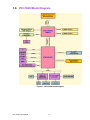
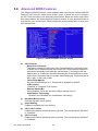
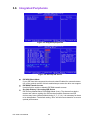
1
User Manual
PCI-7020
PCI Half-sized Intel® LGA775
Processor Card with VGA/Single
Gigabit LAN
Copyright
The documentation and the software included with this product are copyright 2009 by
Advantech Co., Ltd. All rights are reserved. Advantech Co., Ltd. reserves the right to
make improvements in the products described in this manual at any time without
notice. No part of this manual may be reproduced, copied, translated or transmitted
in any form or by any means without the prior written permission of Advantech Co.,
Ltd. Information provided in this manual is intended to be accurate and reliable. However, Advantech Co., Ltd. assumes no responsibility for its use, nor for any infringements of the rights of third parties, which may result from its use.
Acknowledgements
AWARD is a trademark of Phoenix Technologies Ltd.
IBM and PC are trademarks of International Business Machines Corporation.
Intel®, Core™ 2 Duo, Pentium® D, Pentium® 4, and Celeron® D are trademarks of
Intel Corporation.
WinBond is a trademark of Winbond Corporation.
All other product names or trademarks are the properties of their respective owners.
PCI-7020 User Manual
Part No. 2002702000
Edition 1
Printed in China
July 2009
ii
A Message to the Customer
Advantech Customer Services
Each and every Advantech product is built to the most exacting specifications to
ensure reliable performance in the harsh and demanding conditions typical of industrial environments. Whether your new Advantech equipment is destined for the laboratory or the factory floor, you can be assured that your product will provide the
reliability and ease of operation for which the name Advantech has come to be
known.
Your satisfaction is our primary concern. Here is a guide to Advantech’s customer
services. To ensure you get the full benefit of our services, please follow the instructions below carefully.
Technical Support
We want you to get the maximum performance from your products. So if you run into
technical difficulties, we are here to help. For the most frequently asked questions,
you can easily find answers in your product documentation. These answers are normally a lot more detailed than the ones we can give over the phone.
So please consult this manual first. If you still cannot find the answer, gather all the
information or questions that apply to your problem, and with the product close at
hand, call your dealer. Our dealers are well trained and ready to give you the support
you need to get the most from your Advantech products. In fact, most problems
reported are minor and are able to be easily solved over the phone.
In addition, free technical support is available from Advantech engineers every business day. We are always ready to give advice on application requirements or specific
information on the installation and operation of any of our products.
Declaration of Conformity
FCC Class A
Note: This equipment has been tested and found to comply with the limits for a Class
A digital device, pursuant to part 15 of the FCC Rules. These limits are designed to
provide reasonable protection against harmful interference when the equipment is
operated in a commercial environment. This equipment generates, uses, and can
radiate radio frequency energy and, if not installed and used in accordance with the
instruction manual, may cause harmful interference to radio communications. Operation of this equipment in a residential area is likely to cause harmful interference in
which case the user will be required to correct the interference at his own expense.
Caution! There is a danger of a new battery exploding if it is incorrectly installed.
Do not attempt to recharge, force open, or heat the battery. Replace the
battery only with the same or equivalent type recommended by the manufacturer. Discard used batteries according to the manufacturer’s
instructions.
iii
PCI-7020 User Manual
Memory Compatibility
Brand
Apacer(RoHS)
DSL
Kingston(RoHS)
Transcend(RoHS)
Size
Speed
Type
Memory
512 MB
DDR2 533
DDR2
ELPIDA E5108AG-5C-E (64x8)
512 MB
DDR2 667
DDR2
ELPIDA E5108AG-6E-E (64x8)
1 GB
DDR2 533
DDR2
SAMSUNG K4T51083QB-ZKD5
(128x4)
1 GB
DDR2 533
DDR2
ELPIDA E5108AGBG-6E-E (64x8)
1 GB
DDR2 667
DDR2
ELPIDA E5108AGBG-6E-E (64x8)
2 GB
DDR2 667
DDR2
SEC K4T1G08400 (128x8)
512 MB
DDR2 533
DDR2
infineon HYB18T512 800AF37
FSS43331 (64x8)
1 GB
DDR2 533
DDR2
ELPIDA E5108AE-5C-E (64x8)
1 GB
DDR2 667
DDR2
ELPIDA E5108AGBG-6E-E (64x8)
2 GB
DDR2 667
DDR2
ELPIDA E1108ACSE-6E-E(128x8)
2 GB
DDR2 667
DDR2
Micron 7KE12 D9HNL (128x8)
256 MB
DDR2 533
DDR2
infineon HYB18T512160AF3.7
3VV21710 (32x16)
256 MB
DDR2 533
DDR2
SAMSUNG 443 K4T56083QF-GCD5
(32x8)
512 MB
DDR2 533
DDR2
SEC K4T51083QC ZCD5 (64X8)
512 MB
DDR2 667
DDR2
SAMSUNG K4T51083QC ZCE6
(64x8)
1 GB
DDR2 667
DDR2
SEC K4T51083QE ZCE6 (64x8)
1 GB
DDR2 667
DDR2
SEC K4T51083QG HCE6 (64x8)
2 GB
DDR2 667
DDR2
SAMSUNG K4T1G084QD-ZCE6
(128x8)
2 GB
DDR2 667
DDR2
Micron 7HE12 D9HNL (128x8)
2 GB
DDR2 667
DDR2
SAMSUNG K4T1G084QA-ZCE6
(128x8)
Network Feature Comparison
LAN/Model
PCI-7020F
PCI-7020VG
PCI-7020LV
LAN1: Intel® 82574L
Yes
Yes
No
PCI-7020 User Manual
iv
Processor Support
Intel Core™ 2 Duo Desktop Processor
Long-term supported P/N: E7400, E6400,
Intel® Pentium® Dual-Core Desktop Processor
E4300, E2160, Celeron 440
Intel Celeron® Processor 400
Intel Pentium D Processor
Intel Pentium 4 Processor
Intel Celeron D Processor
Note!
PCI-7020 CPU cooler (p/n:1960035861N000), It must use the CPU thermal design power lower than 65 Watt.
Product Warranty (2 years)
Advantech warrants to you, the original purchaser, that each of its products will be
free from defects in materials and workmanship for two years from the date of purchase.
This warranty does not apply to any products which have been repaired or altered by
persons other than repair personnel authorized by Advantech, or which have been
subject to misuse, abuse, accident or improper installation. Advantech assumes no
liability under the terms of this warranty as a consequence of such events.
Because of Advantech’s high quality-control standards and rigorous testing, most of
our customers never need to use our repair service. If an Advantech product is defective, it will be repaired or replaced at no charge during the warranty period. For outof-warranty repairs, you will be billed according to the cost of replacement materials,
service time and freight. Please consult your dealer for more details.
If you think you have a defective product, follow these steps:
1. Collect all the information about the problem encountered. (For example, CPU
speed, Advantech products used, other hardware and software used, etc.) Note
anything abnormal and list any onscreen messages you get when the problem
occurs.
2. Call your dealer and describe the problem. Please have your manual, product,
and any helpful information readily available.
3. If your product is diagnosed as defective, obtain an RMA (return merchandise
authorization) number from your dealer. This allows us to process your return
more quickly.
4. Carefully pack the defective product, a fully-completed Repair and Replacement
Order Card and a photocopy proof of purchase date (such as your sales receipt)
in a shippable container. A product returned without proof of the purchase date
is not eligible for warranty service.
5. Write the RMA number visibly on the outside of the package and ship it prepaid
to your dealer.
v
PCI-7020 User Manual
Initial Inspection
Before you begin installing your single board computer, please make sure that the
following materials have been shipped:
!
!
!
!
!
!
!
!
!
!
!
!
!
!
PCI-7020 Intel® LGA775 processor-based single
board computer
1 PCI-7020 user manual
1 CD with driver utility and manual (in PDF format)
2 Power cable 12P / Big 4P
1 Dual COM cable 2.0 mm pitch
1 Serial ATA HDD data cable
1 Serial ATA HDD power cable
1 Printer port cable 2.0 mm pitch
1 Y cable for PS/2 keyboard and PS/2 mouse
1 USB cable with 4 ports
ATX feature cable
1 Jumper pack
CPU cooler
1 warranty card
P/N: 1700006196
P/N: 1700008762
P/N: 1700003194
P/N: 1703150102
P/N: 1700002223
P/N: 1700060202
P/N: 1700014398
P/N: 1700002343
P/N: 9689000002
P/N: 1960035861N000
If any of these items are missing or damaged, contact your distributor or sales representative immediately. We have carefully inspected the PCI-7020 mechanically and
electrically before shipment. It should be free of marks and scratches and in perfect
working order upon receipt. As you unpack the PCI-7020, check it for signs of shipping damage. (For example, damaged box, scratches, dents, etc.) If it is damaged or
it fails to meet the specifications, notify our service department or your local sales
representative immediately. Also notify the carrier. Retain the shipping carton and
packing material for inspection by the carrier. After inspection, we will make arrangements to repair or replace the unit.
Note!
PCI-7020 CPU cooler (p/n:1960035861N000), It must use the CPU thermal design power lower than 65 Watt.
PCI-7020 User Manual
vi
Contens
Chapter
1
Hardware Configuration......................1
1.1
1.2
1.3
Introduction ............................................................................................... 2
Features .................................................................................................... 2
Specifications ............................................................................................ 3
1.3.1 System .......................................................................................... 3
1.3.2 Memory ......................................................................................... 3
1.3.3 Input/Output .................................................................................. 3
1.3.4 Ethernet LAN ................................................................................ 3
1.3.5 Industrial Features ........................................................................ 3
1.3.6 Mechanical and Environmental Specifications.............................. 3
Jumpers and Connectors .......................................................................... 4
Table 1.1: Jumpers...................................................................... 4
Table 1.2: Connectors ................................................................. 4
Board Layout: Jumper and Connector ...................................................... 5
Figure 1.1 Jumper and connector location (top) .......................... 5
Figure 1.2 Jumper and connector location (bot) .......................... 5
PCI-7020 Block Diagram........................................................................... 6
Figure 1.3 PCI-7020 block diagram ............................................. 6
Safety Precautions .................................................................................... 7
Jumper Settings ........................................................................................ 7
1.8.1 How to Set Jumpers...................................................................... 7
1.8.2 CMOS Clear (CMOS1) ................................................................. 7
Table 1.3: CMOS (CMOS1)......................................................... 8
1.8.3 Watchdog Timer Output (JWDT1) ................................................ 8
Table 1.4: Watchdog Timer Output (JWDT1) .............................. 8
System Memory ........................................................................................ 8
1.9.1 CPU FSB and Memory Speed ...................................................... 8
Memory Installation Procedures................................................................ 8
Cache Memory.......................................................................................... 9
Processor Installation................................................................................ 9
Power Model Setting and Installation...................................................... 10
Figure 1.4 ATX power setting of PCI-7020 with backplane ....... 10
Figure 1.5 ATX power setting of PCI-7020 with single board .... 10
Figure 1.6 AT power setting of PCI-7020 with backplane.......... 11
Figure 1.7 AT power setting of PCI-7020 with single board ...... 11
1.4
1.5
1.6
1.7
1.8
1.9
1.10
1.11
1.12
1.13
Chapter
2
Connecting Peripherals ....................13
2.1
2.2
2.3
2.4
2.5
2.6
2.7
2.8
2.9
Introduction ............................................................................................. 14
Parallel Port (LPT1)................................................................................. 14
VGA Connector (VGA1) .......................................................................... 15
Serial Ports (COM1, COM2) ................................................................... 15
PS/2 Keyboard and Mouse Connector (KBMS1) .................................... 16
External Keyboard & Mouse (KBMS2).................................................... 16
CPU Fan Connector (CPUFAN1)............................................................ 17
Front Panel Connectors (JFP1, JFP2) .................................................... 17
H/W Monitor Alarm (JOBS1) ................................................................... 18
Table 2.1: Hardware Monitor Alarm Setting .............................. 18
LAN RJ45 Connector (LAN1).................................................................. 18
HD Link Connector (HDAUD1)................................................................ 19
Serial ATA2 Interface (SATA1 ~ SATA3)................................................ 19
LAN LED Connector (LAN LED1) ........................................................... 20
Table 2.2: Front Panel LAN Indicator Connector....................... 20
USB (USB12, USB34, USB56) ............................................................... 21
2.10
2.11
2.12
2.13
2.14
vii
PCI-7020 User Manual
Chapter
2.15
Case Open (JCASE1)............................................................................. 21
3
Award BIOS Setup ............................ 23
3.1
Introduction ............................................................................................. 24
3.1.1 CMOS RAM Auto-backup and Restore ...................................... 24
Entering Setup ........................................................................................ 24
Figure 3.1 Award BIOS setup initial screen............................... 24
Standard CMOS Setup ........................................................................... 25
Figure 3.2 Standard CMOS features screen ............................. 25
Advanced BIOS Features ....................................................................... 26
Figure 3.3 Advanced BIOS features screen .............................. 26
Advanced Chipset Features.................................................................... 28
Figure 3.4 Advanced chipset features screen ........................... 28
Integrated Peripherals............................................................................. 30
Figure 3.5 Integrated peripherals .............................................. 30
Figure 3.6 On-Chip IDE device.................................................. 30
Figure 3.7 Onboard device ........................................................ 31
Figure 3.8 Super I/O device....................................................... 32
Power Management Setup ..................................................................... 34
Figure 3.9 Power management setup screen............................ 34
Figure 3.10Power management setup screen (Conn.)............... 34
Table 3.1: Power Saving ........................................................... 35
PnP/PCI Configurations .......................................................................... 36
Figure 3.11PnP/PCI configurations screen ................................ 36
PC Health Status .................................................................................... 37
Figure 3.12PC health status screen ........................................... 37
Frequency / Voltage Control ................................................................... 38
Figure 3.13Spread spectrum control screen .............................. 38
Password Setting .................................................................................... 39
Figure 3.14Enter password ........................................................ 39
Load Setup Defaults ............................................................................... 40
Figure 3.15 Load setup defaults screen ..................................... 40
Save & Exit Setup ................................................................................... 41
Figure 3.16Save to CMOS and Exit ........................................... 41
Exit Without Saving................................................................................. 42
Figure 3.17Quit Without Saving.................................................. 42
3.2
3.3
3.4
3.5
3.6
3.7
3.8
3.9
3.10
3.11
3.12
3.13
3.14
Chapter
Chapter
Chapter
4
Chipset Software Installation Utility 43
4.1
4.2
4.3
Before You Begin.................................................................................... 44
Introduction ............................................................................................. 44
Windows XP Driver Setup....................................................................... 45
5
VGA Setup ......................................... 49
5.1
5.2
Introduction ............................................................................................. 50
Windows XP Driver Setup....................................................................... 50
6
LAN Configuration ............................ 55
6.1
6.2
6.3
6.4
Introduction ............................................................................................. 56
Features.................................................................................................. 56
Installation............................................................................................... 56
Win XP Driver Setup ............................................................................... 57
PCI-7020 User Manual
viii
Appendix A
Programming the Watchdog Timer..59
A.1
Programming the Watchdog Timer ......................................................... 60
A.1.1 Watchdog timer overview............................................................ 60
A.1.2 Jumper selection......................................................................... 60
A.1.3 Programming the Watchdog Timer ............................................. 60
Table A.1: Watchdog Timer Registers ....................................... 62
A.1.4 Example Program ....................................................................... 63
Appendix B
I/O Pin Assignments..........................67
B.1
Front Panel Connectors (JFP1) .............................................................. 68
Table B.1: Front Panel Connectors (JFP1)................................ 68
USB Ports (USB12/USB34) .................................................................... 68
Table B.2: USB Ports (USB12/USB34)...................................... 68
IR Connector (JIR1) ................................................................................ 69
Table B.3: IR Connector (JIR1).................................................. 69
Serial Ports (COM12).............................................................................. 69
Table B.4: Serial Ports (COM12) ............................................... 69
PS/2 Keyboard / Mouse Connector (KBMS2) ......................................... 70
Table B.5: PS/2 Keyboard / Mouse Connector (KBMS2) .......... 70
LAN LED Connector (LANLED1) ............................................................ 70
Table B.6: LAN LED Connector (LANLED1/LANLED2)............. 70
ATX Feature Connector (ATXF1)............................................................ 70
Table B.7: ATX Feature Connector (ATXF1) ............................. 70
CPU FAN Connector (CPUFAN1)........................................................... 71
Table B.8: CPU FAN Connector (CPUFAN1) ............................ 71
System FAN Connector (SYSFAN1)....................................................... 71
Table B.9: System FAN Cconnector (SYSFAN1) ...................... 71
Audio Interface Connector (HDAUD1) .................................................... 71
Table B.10:Audio Interface Connector (HDAUD1)...................... 71
GPIO Header (GPIO1) ............................................................................ 72
Table B.11:GPIO Header (GPIO1) ............................................. 72
DVI LCD Panel Connector (DVI1)........................................................... 72
Table B.12:DVI LCD Panel Connector (DVI1) ............................ 72
Low Pin Count Header (LPC1)................................................................ 73
Table B.13:Low Pin Count Header (LPC1) ................................. 73
ATX Power Control Connector (ATX1) ................................................... 73
Table B.14:ATX Power Control Connector (ATX1)..................... 73
VGA Connector (VGA1) .......................................................................... 74
Table B.15:VGA Connector (VGA1) ........................................... 74
H/W Monitor Alarm (JOBS1) ................................................................... 74
Table B.16:H/W Monitor Alarm (JOBS1) .................................... 74
Watchdog Timer Output (JWDT1)........................................................... 74
Table B.17: Watchdog Timer Output (JWDT1) ........................... 74
B.2
B.3
B.4
B.5
B.6
B.7
B.8
B.9
B.10
B.11
B.12
B.13
B.14
B.15
B.16
B.17
Appendix C
System Assignments ........................77
C.1
System I/O Ports ..................................................................................... 78
Table C.1: System I/O Ports ...................................................... 78
DMA Channel Assignments .................................................................... 79
Table C.2: DMA Channel Assignments...................................... 79
Interrupt Assignments ............................................................................. 79
Table C.3: Interrupt Assignments............................................... 79
1st MB Memory Map ............................................................................... 79
Table C.4: 1st MB Memory Map ................................................ 79
C.2
C.3
C.4
ix
PCI-7020 User Manual
PCI-7020 User Manual
x
Chapter
1
Hardware
Configuration
1
1.1 Introduction
The PCI-7020 is a half-size CPU card designed with the Intel® 945GC and ICH7R
chipset (I/O controller) to support Core® 2 Duo / Dual-Core Pentium® / Pentium® 4 /
Celeron® D processors (refer to "Processor Support" on page v) with a 533/800/1066
MHz front side bus and DDR2 533/667 MHz memory up to 4 GB. It is the best solution for high-performance computing and applications in which a wide I/O bandwidth
is demanded.
The PCI-7020 offers a high-performance cost-saving integrated graphics unit, built
into the Intel® 945GC chipset, and features the unique Intel® Extreme Graphics
architecture to maximize VGA performance and share system memory up to 224 MB.
It has 2 SODIMM sockets in two separated memory channels. It accepts up to 4 GB
DDR2 SDRAM memory, enough for most applications. The PCI-7020 has a single
Gigabit Ethernet LAN via dedicated PCI Express x 1 bus, which offers bandwidths up
to 500 MB/s, eliminating network data flow bottlenecks, and incorporating Gigabit
Ethernet. High reliability and outstanding performance make the PCI-7020 the ideal
platform for industrial networking applications.
Three Serial ATA2 ports (up to 300 MB/s) allow the use of thin and long SATA cables
for storage devices, eliminating cabling issues inside the industrial-grade chassis. In
addition, the PCI-7020 also provides most of the popular I/O interfaces such as six
USB 2.0 ports, 2 RS-232 ports and enhanced parallel port interface.
The PCI-7020 is designed with consideration for extended reliability, and is built
especially to suit demanding industrial environments. The CMOS data backup and
restore function protects the BIOS setup data from loss due to battery failure.
1.2 Features
!
!
!
!
!
!
!
Supports LGA 775 Intel® Core® 2 Duo / Pentium® Dual-Core / Pentium® D /
Pentium® 4 / Celeron® 400 / Celeron® D FSB 533/800/1066 MHz processors
(refer to "Processor Support" on page v)
Supports Dual Channel DDR2 533/667 SDRAM up to 4 GB
Single Gigabit Ethernet via PCI Express x1 port
3 SATA2 connector; supports S/W RAID 0, 1 (LV sku has NO S/W RAID)
6 USB 2.0 ports
6 COM port supports (2 ports RS-232, and can add optional 4 port RS-232/422/
485 by PCA-COM232 or PCA-COM485 module)
CMOS automatic backup and restore to prevent accidental data loss of BIOS
setup
PCI-7020 User Manual
2
1.3.1 System
!
!
1.3.2 Memory
!
RAM: Up to 4 GB in two 200-pin SODIMM sockets. Supports dual-channel
DDRII 533/667 SDRAM.
1.3.3 Input/Output
!
!
!
!
!
PCI bus: 32 bit / 33MHz to the backplane
Parallel port: One EPP/ECP parallel port
Serial ports: Two serial RS-232 ports (and can add optional 4 port RS-232/422/
485 by PCA-COM232 or PCA-COM485 module)
Keyboard and PS/2 mouse connector: One 6-pin mini-DIN connector is
located on the mounting bracket for easy connection to a keyboard or PS/2
mouse. An on board keyboard pin header connector is also available
USB port: Supports up to six USB 2.0 ports with transmission rate up to 480
Mbps (2 ports on rear I/O, 4 ports onboard by 2.0 mm pitch box header)
1.3.4 Ethernet LAN
!
!
Supporting single 10/100/1000Base-T Ethernet port(s) via PCI Express x1 bus
which provides 500 MB/s data transmission rate
Controller:
– LAN 1: Intel® 82574L
1.3.5 Industrial Features
Watchdog timer: Can generate a system reset. The watchdog timer is pro-grammable to 255 levels, with each unit set to equal either one second or one minute.
1.3.6 Mechanical and Environmental Specifications
!
!
!
!
!
!
!
Operating temperature: 0 ~ 60° C (32 ~ 140° F, depending on CPU)
Operating humidity: 40° C @ 85% RH Non-Condensing
Storage temperature: -40 ~ 85° C (-40 ~ 185° F) non-condensing
Power supply voltage: +5 V, +12 V, +5 VSBY
Power consumption: +5 V @ 4.86 A, +12 V @ 4.38 A, +5 VSB @ 0.39 A (Intel
Core 2 Duo 2.8 GHz, 65 W, 800 MHz FSB + 2 x 2 GB DDR2 667)
Board size: 185 x 122 mm (7.28" x 4.8")
Board weight: 0.185 kg (0.4 lbs.)
3
PCI-7020 User Manual
Hardware Configuration
!
!
!
CPU: Intel® LGA 775 Core® 2 Duo, Pentium Dual-Core, Pentium 4, Celeron D
up to 2.93/2.7/3.4/3.6 GHz, (refer to "Processor Support" on page v), FSB 533/
800/1066 MHz.
L2 cache: CPU has built-in 4 MB (for Core® 2 Duo), 2 MB (for Pentium DualCore CPU), 2 MB (for Pentium 4 CPU), 512 KB (for Celeron D CPU) full-speed
L2 cache
BIOS: Award Flash BIOS (8 MB Flash Memory)
System chipset: Intel 945GC with ICH7R/ICH7
SATA hard disk drive interface: Three on-board SATA2 connectors with data
transmission rate up to 300 MB/s; supports S/W RAID 0, 1 (LV sku has NO S/W
RAID)
Chapter 1
1.3 Specifications
1.4 Jumpers and Connectors
Connectors on the PCI-7020 single board computer link to external devices such as
hard disk drives and a keyboard. In addition, the board has a number of jumpers
used to configure the system for any desired application.
The tables below list the function of each of the board jumpers and connectors. Later
sections in this chapter give instructions on setting jumpers. Chapter 2 gives instructions for connecting external devices to the motherboard.
Table 1.1: Jumpers
Label
Function
CMOS1
CMOS clear
JWDT1
Watchdog timer output selection
Table 1.2: Connectors
Label
Function
LPT1
Parallel port
VGA1
VGA connector
CF1
CF socket
COM12
RS232 serial ports connector
KBMS1
PS/2 keyboard and mouse connector
KBMS2
External keyboard/mouse connector
JIR1
Infrared connector
JOBS1
HW Monitor Alarm
Close: Enable OBS Alarm
Open: Disable OBS Alarm
CPUFAN1
CPU FAN connector
JFP1
Power and Reset Button connector
JFP2
HDD LED/Speaker connector
LAN1
LAN RJ45 connector
LANLED1
LAN1 LED connector
HDAUD1
HD Audio connector
SATA1
Serial ATA1
SATA2
Serial ATA2
SATA3
Serial ATA3
USB12
Two USB port pin headers
USB34
Two USB port pin headers
USB5
USB connector
USB6
USB connector
DIMMA1
Memory connector channel A
DIMMB1
Memory connector channel B
LPC1
Low pin count connector
SPI1
BIOS SPI Interface
JCASE1
Case open
DVI1
DVI connector (only for F sku)
PCI-7020 User Manual
4
Figure 1.2 Jumper and connector location (bot)
5
PCI-7020 User Manual
Hardware Configuration
Figure 1.1 Jumper and connector location (top)
Chapter 1
1.5 Board Layout: Jumper and Connector
1.6 PCI-7020 Block Diagram
Figure 1.3 PCI-7020 block diagram
PCI-7020 User Manual
6
Warning! Always completely disconnect the power cord from your chassis whenever you work with the hardware. Do not make connections while the
power is on. Sensitive electronic components can be damaged by sudden power surges. Only experienced electronics personnel should open
the PC chassis.
Caution! The computer is provided with a battery-powered real-time clock circuit.
There is a danger of explosion if battery is incorrectly replaced. Replace
only with same or equivalent type recommended by the manufacturer.
Discard used batteries according to manufacturer's instructions.
Caution! There is a danger of a new battery exploding if it is incorrectly installed.
Do not attempt to recharge, force open, or heat the battery. Replace the
battery only with the same or equivalent type recommended by the manufacturer. Discard used batteries according to the manufacturer's
instructions.
1.8 Jumper Settings
This section provides instructions on how to configure your PCI-7020 by setting the
jumpers. It also includes the PCI-7020's default settings and your options for each
jumper.
1.8.1 How to Set Jumpers
You can configure your PCI-7020 to match the needs of your application by setting
the jumpers. A jumper is a metal bridge that closes an electrical circuit. It consists of
two metal pins and a small metal clip (often protected by a plastic cover) that slides
over the pins to connect them. To "close" (or turn ON) a jumper, you connect the pins
with the clip. To "open" (or turn OFF) a jumper, you remove the clip. Sometimes a
jumper consists of a set of three pins, labeled 1, 2, and 3. In this case you connect
either pins 1 and 2, or 2 and 3. A pair of needle-nose pliers may be useful when setting jumpers.
1.8.2 CMOS Clear (CMOS1)
The PCI-7020 single board computer contains a jumper that can erase CMOS data
and reset the system BIOS information. Normally this jumper should be set with pins
1-2 closed. If you want to reset the CMOS data, set CMOS1 to 2-3 closed for just a
few seconds, and then move the jumper back to 1-2 closed. This procedure will reset
the CMOS to its default setting.
7
PCI-7020 User Manual
Hardware Configuration
Caution! Always ground yourself to remove any static charge before touching the
boards. Modern electronic devices are very sensitive to static electric
charges. As a safety precaution, use a grounding wrist strap at all times.
Place all electronic components on a static- dissipative surface or in a
static-shielded bag when they are not in the chassis.
Chapter 1
1.7 Safety Precautions
Table 1.3: CMOS (CMOS1)
Function
Jumper Setting
1
Keep CMOS data *
1-2 closed
1
Clear CMOS data
2-3 closed
*default setting
1.8.3 Watchdog Timer Output (JWDT1)
The PCI-7020 contains a watchdog timer that will reset the CPU in the event the CPU
stops processing. This feature means the PCI-7020 will recover from a soft- ware failure or an EMI problem. The JWDT1 jumper settings control the outcome of what the
computer will do in the event the watchdog timer is tripped.
Table 1.4: Watchdog Timer Output (JWDT1)
Function
Jumper Setting
1
NC
1-2 closed
1
Reset*
2-3 closed
*default setting
1.9 System Memory
The PCI-7020 has two sockets for 200-pin dual inline memory modules (SODIMMs)
in two memory channels. All these sockets use 1.8 V unbuffered double data rate
synchronous DRAMs (DDR2 SDRAM). They are available in capacities of 256, 512,
1024 and 2048 MB. The sockets can be filled in any combination with DIMMs of any
size, giving a total memory size between 256 MB and 4 GB.
1.9.1 CPU FSB and Memory Speed
The PCI-7020 supports Intel LGA775 CPUs with FSB 533/800/1066. The PCI-7020
can accept DDR2 SDRAM memory chips without parity. Also note: The PCI-7020
accepts DDR2 533/667MHz SDRAM. The PCI-7020 does NOT support ECC (error
checking and correction).
1.10 Memory Installation Procedures
To install DIMMs, slowly slide the DIMM module along the plastic guides on both
ends of the socket. Then press the DIMM module right down into the socket, until you
hear a click. This is when the two handles have automatically locked the memory
module into the correct position of the DIMM socket.
PCI-7020 User Manual
8
PCI-7020 supports built-in 4 MB CPU cache (for Core® 2 Duo), 2 MB (for Pentium
Dual-Core CPU), 2 MB (for Pentium 4 CPU), 512 KB (for Celeron D) L2 cache. The
built-in second-level cache in the processor yields much higher performance than
conventional external cache memories.
1.12 Processor Installation
2.
Align the triangular marking on the processor with the cut edge of the socket.
Step 3. Put back the socket cap and press down the bar to fix it.
9
PCI-7020 User Manual
Hardware Configuration
PCI-7020 is designed for Intel® LGA 775 socket CPUs.
Step 1. Pull the bar beside the CPU socket outward and lift it.
Chapter 1
1.11 Cache Memory
1.13 Power Model Setting and Installation
PCI-7020 can support AT or ATX power model settings. It can be used with backplanes and single boards.
Installation as below.
ATX Power Supply
With backplane
Please refer to Figure 1.4
1.
Use 3 pin ATX signal cable (P/N:1700002343) to connect the ATXF1
on the CPU card with PS-ON (CN1) on the backplane.
2.
Use power cable (P/N:1700006196) to connect power supply with
ATX1 connector on the CPU card.
3.
Connect the power supply and ATX1 connector on the backplane.
Single board
Please refer to Figure 1.5
1.
Remove the jumper on CPU card ATXF1 1-2 pins.
2.
Use power cable (P/N:1700000265) to connect the power supply with
the ATX1 connector on the CPU card.
Figure 1.4 ATX power setting of PCI-7020 with backplane
Figure 1.5 ATX power setting of PCI-7020 with single board
PCI-7020 User Manual
10
Single board
Please refer to Figure 1.7
1.
Short ATXF1 1-2 pins on CPU card.
2.
Use the power cable (P/N:1700006196) to connect the power supply
with the ATX1 connector on the CPU card.
Figure 1.6 AT power setting of PCI-7020 with backplane
Figure 1.7 AT power setting of PCI-7020 with single board
11
PCI-7020 User Manual
Hardware Configuration
With backplane
Please refer to Figure 1.6
1.
Short ATXF1 1-2 pins on CPU card and PS-ON(CN1) 1-2 pins on
backplane.
2.
Use power cable (P/N:1700006196) to connect the power supply with
ATX1 connector on CPU card.
3.
Connect the power supply and the ATX1 connector on the backplane.
Chapter 1
AT Power Supply
PCI-7020 User Manual
12
Chapter
2
Connecting
Peripherals
2
2.1 Introduction
You can access most of the connectors from the top of the board while it is installed
in the chassis. If you have a number of cards installed or have a packed chassis, you
may need to partially remove the card to make all the connections.
2.2 Parallel Port (LPT1)
The parallel port is normally used to connect the single board computer to a printer.
The PCI-7020 includes an onboard parallel port, accessed through a 26-pin flatcable connector, LPT1. The card comes with an adapter cable which lets you use a
traditional DB-25 connector. The cable has a 26-pin connector on one end and a DB25 connector on the other, mounted on a retaining bracket. The bracket installs at the
end of an empty slot in your chassis, giving you access to the connector.
To install the bracket, find an empty slot in your chassis. Unscrew the plate that covers the end of the slot. Screw in the bracket in place of the plate. Next, attach the flatcable connector to LPT1 on the CPU card. Wire 1 of the cable is red or blue, and the
other wires are gray. Make sure that wire 1 corresponds to pin 1 of LPT1. Pin 1 is on
the upper right side of LPT1.
PCI-7020 User Manual
14
Chapter 2
2.3 VGA Connector (VGA1)
2.4 Serial Ports (COM1, COM2)
The PCI-7020 offers two serial ports COM1, COM2. These ports can connect to
serial devices, such as a mouse or to a communications network.
The IRQ and address ranges for all ports are fixed. However, if you want to disable
the port or change these parameters later, you can do this in the system BIOS setup.
Different devices implement the RS-232 standard in different ways. If you are having
problems with a serial device, be sure to check the pin assignments for the connector.
15
PCI-7020 User Manual
Connecting Peripherals
The PCI-7020 includes a VGA interface that can drive conventional CRT displays.
VGA1 is a standard 15-pin D-SUB connector commonly used for VGA. Pin assignments for CRT connector VGA1 are detailed in Appendix B.
2.5 PS/2 Keyboard and Mouse Connector (KBMS1)
One 6-pin mini-DIN connectors (KBMS1) on the card mounting bracket provide connection to a PS/2 keyboard or a PS/2 mouse, respectively. KBMS1 can also be connected to an adapter cable (P/N: 1700060202) for connecting to both a PS/2 keyboard and a PS/2 mouse.
2.6 External Keyboard & Mouse (KBMS2)
In addition to the PS/2 mouse/keyboard connector on the PCI-7020's rear plate,
there is also an extra onboard external keyboard and mouse connector. This gives
system integrators greater flexibility in designing their systems.
PCI-7020 User Manual
16
Chapter 2
2.7 CPU Fan Connector (CPUFAN1)
2.8 Front Panel Connectors (JFP1, JFP2)
There are several external switches to monitor and control the PCI-7020.
17
PCI-7020 User Manual
Connecting Peripherals
If a fan is used, this connector supports cooling fans of 12 V/1 A (12 W) or less.
2.9 H/W Monitor Alarm (JOBS1)
(JOBS1) is a 2-pin jumper to enable/disable the alarm for on board security events.
Table 2.1: Hardware Monitor Alarm Setting
Pin Setting
Function
closed
Enable OBS alarm
open
Disable OBS alarm
2.10 LAN RJ45 Connector (LAN1)
PCI-7020 uses the Intel 82574L Gigabit LAN chip which is linked to PCIe x1 link.
With this chip, PCI-7020 may provide high throughputs for a heavy load networking
environment. It provides one or two RJ-45 connectors in the rear side and is convenient for most industrial applications.
PCI-7020 User Manual
18
Chapter 2
2.11 HD Link Connector (HDAUD1)
2.12 Serial ATA2 Interface (SATA1 ~ SATA3)
The PCI-7020 features a high performance serial ATA2 interface (up to 300MB/s)
which eases cabling to hard drives with thin and long cables.
19
PCI-7020 User Manual
Connecting Peripherals
The PCI-7020 provides HD audio through PCA-AUDIO-HDA1 module from Advantech.
2.13 LAN LED Connector (LAN LED1)
PCI-7020 provides an external LAN LED Pin header for connecting to the front side
of the chassis. With this convenient design users can easily see whether the LAN
port is active or not. Refer to Appendix B for detailed information on the pin assignments.
Table 2.2: Front Panel LAN Indicator Connector
LAN Mode
1000 Mbps
100 Mbps
10 Mbps
PCI-7020 User Manual
LED1
LED2
Link On
Green On
On
Active
Green on
Green Flashes
Link Off
Off
Off
Link On
Orange On
Green On
Active
Orange On
Green Flashes
Link Off
Off
Off
Link On
Off
Green On
Active
Off
Green Flashes
Link Off
Off
Off
20
Chapter 2
2.14 USB (USB12, USB34, USB56)
2.15 Case Open (JCASE1)
PCI-7020 provides 2-Pins pin header for case open detection. This function could be
enabled or disabled in the BIOS setting. When the PIN is shorted, it will cause the on
board buzzer to sound.
21
PCI-7020 User Manual
Connecting Peripherals
The PCI-7020 board provides up to Six USB (Universal Serial Bus) ports. This gives
complete Plug and Play, and hot attach/detach for up to 127 external devices. The
USB interfaces comply with USB specification Rev. 2.0, and are fuse protected. The
USB interface is accessed through the 5 x 2-pin flat-cable connector, CN9 (USB0, 1),
CN10 (USB2, 3). You will need an adapter cable if you use a standard USB connector. The adapter cable has a 5 x 2-pin connector on one end and a USB connector on
the other. The USB interfaces can be disabled in the system BIOS setup.
PCI-7020 User Manual
22
Chapter
3
3
Award BIOS Setup
3.1 Introduction
Award’s BIOS ROM has a built-in setup program that allows users to modify the
basic system configuration. This type of information is stored in battery backed-up
memory (CMOS RAM) so that it retains the setup information when the power is
turned off.
3.1.1 CMOS RAM Auto-backup and Restore
The CMOS RAM is powered by an onboard button cell battery. When you finish BIOS
setup, the data in CMOS RAM will be automatically backed up to Flash ROM. If operation in harsh industrial environments causes a soft error, BIOS will recheck the data
in CMOS RAM and automatically restore the original data in Flash ROM to CMOS
RAM for booting.
Note!
If you intend to change the CMOS setting without restoring the previous
backup, you have to click on “DEL” within two seconds of the “CMOS
checksum error...” display screen message appearing. Then enter the
“Setup” screen to modify the data. If the “CMOS checksum error...” message appears again and again, please check to see if you need to
replace the battery in your system.
3.2 Entering Setup
Turn on the computer and press <Del> to enter the BIOS setup.
Figure 3.1 Award BIOS setup initial screen
PCI-7020 User Manual
24
!
!
!
!
Figure 3.2 Standard CMOS features screen
25
PCI-7020 User Manual
Award BIOS Setup
!
Date
The date format is <week>, <month>, <day>, <year>.
Time
The time format is <hour> <minute> <second>, based on the 24-hour clock.
IDE channel 0/1 Master/Slave
– IDE HDD Auto-Detection: Press “Enter” to select this option for automatic
device detection.
– IDE Device Setup:
Auto: Automatically detects IDE devices during POST
None: Select this when no IDE device is used. The system will skip the autodetection step to make system start up faster.
Manual: User can manually input the correct settings.
– Access Mode: The options are CHS/LBA/Large/Auto
– Capacity: Capacity of currently installed hard disk.
– Cylinder: Number of cylinders
– Head: Number of heads
– Precomp: Write precomp
– Landing Zone: Landing zone
– Sector: Number of sectors
Halt On
This category determines whether system start-up will halt or not when an error
is detected during power up.
The options are: No Errors/All Errors/All, But Keyboard/All, But Diskette/All, But
Disk/Key
Memory
This category displays base memory, extended memory, and total memory
detected during POST (Power On Self Test).
Chapter 3
3.3 Standard CMOS Setup
3.4 Advanced BIOS Features
The “Advanced BIOS Features” screen appears when choosing the “Advanced BIOS
Features” item from the “Initial Setup Screen” menu. It allows the user to configure
the PCI-7020 according to his particular requirements. Below are some major items
that are provided in the Advanced BIOS Features screen. A quick booting function is
provided for your convenience. Simply enable the Quick Booting item to save yourself valuable time.
Figure 3.3 Advanced BIOS features screen
!
!
!
!
!
CPU Features
– Delay Prior to thermal
This feature controls the activation of the Thermal Monitor's automatic mode.
It allows you to determine when the Pentium 4's Thermal Monitor should be
activated in automatic mode after the system boots. For example, with the
default value of 16 Minutes, the BIOS activates the Thermal Monitor in automatic mode 16 minutes after the system starts booting up. The choices are 4
Min, 8 Min, 16 Min, and 32 Min.
– Limit CPUID MaxVal
Set Limit CPUID MaxVa1 to 3. This should be disabled for WinXP.
– C1E Function
"Enabled" or "Disabled" C1E function.
– Execute Disable Bit
When disabled, forces the XD feature flag to always return 0.
– Virtualization Technology
"Enabled" and "Disabled" the Virtualization Technology
Hard Disk Boot Priority
Set hard disk boot device priority.
Virus Warning
Enables or disables the virus warning.
CPU L1& L2 Cache
Enabling this feature speeds up memory access. The commands are “Enabled”
or “Disabled.”
CPU L3 Cache
Enabling this feature speeds up memory access. The commands are “Enabled”
or “Disabled”.
PCI-7020 User Manual
26
!
!
!
!
!
!
!
Note!
!
!
!
To disable security, select PASSWORD SETTING in the main menu.
Then, you will be asked to enter a password. Simply press <Enter> to
disable security. When security is disabled, the system will boot and you
can enter Setup freely.
APIC Mode
This setting allows you to enable the APIC mode. The choices are “Disabled” or
“Enabled.”
MPS Version Control For OS
This setting allows you to select the MPS version.The choices are "1.1” or "1.4".
Debug Port Selector: PCI
Select port 80 error code forward to PCI/LPC.
27
PCI-7020 User Manual
Award BIOS Setup
!
Quick Power On Self Test
This allows the system to skip certain tests to speed up the boot-up procedure.
First/Second/Third Boot Device
The BIOS tries to load the OS with the devices in the sequence selected.
Choices are: “LS120”, “Hard Disk”, “CDROM”, “ZIP100”, “USB-FDD”, “USBZIP”, “USB-CDROM”, “LAN1”, “LAN2” and “Disabled”.
Boot Other Device
Use this to boot another device. The options are “Enabled” and “Disabled”.
Boot Up NumLock Status
Sets the boot up status Num Lock. The options are “On” and “Off”.
Gate A20 Option
“Normal”: A pin in the keyboard controller controls GateA20. Fast (Default) lets
chipset control GateA20.
Typematic Rate Setting
The typematic rate is the rate key strokes repeat when a keypress is held. The
commands are “Enabled” or “Disabled”. Enabling allows the typematic rate and
delay to be selected.
Typematic Rate (Chars/Sec)
The BIOS accepts the following input values (characters/second) for typematic
auto repeat rate: 6, 8, 10, 12, 15, 20, 24, and 30.
Typematic Delay (msec)
Typematic delay is the keypress time interval before auto repetition begins. The
input values for this category are: 250, 500, 750, and 1000 (ms).
Security Option
This category determines whether the password is required when the system
boots up or only when entering setup. The options are:
– System: The system will not boot, and access to Setup will be also denied
unless the correct password is entered at the prompt.
– Setup: The system will boot, but access to Setup will be denied unless the
correct password is entered at the prompt.
Chapter 3
!
3.5 Advanced Chipset Features
By choosing the “Advanced Chipset Features” option from the “Initial Setup Screen”
menu, the screen below will be displayed. This sample screen contains the manufacturer’s default values for the PCI-7020, as shown in Figure 3.4:
Figure 3.4 Advanced chipset features screen
Note!
!
!
!
!
!
DRAM default timings have been carefully chosen and should ONLY be
changed if data is being lost. Please first contact technical support.
DRAM Timing Selectable
This item allows you to control the DRAM speed. The selections are “Manual” or
“By SPD”.
CAS Latency Time
When DRAM Timing Selectable is set to [Manual], this field is adjustable. This
controls the CAS latency, which determines the time interval between SDRAM
starting a read command and receiving it. The options are [3T], [4T], [5T], [6T]
and [Auto].
DRAM RAS# to CAS# Delay
When DRAM Timing selectable is set to [Manual], this field is adjustable. When
DRAM is refreshed, the rows and columns are addressed separately. This setup
item allows users to determine the timing of the transition from RAS (row
address strobe) to CAS (column address strobe). The less the clock cycles are,
the faster the DRAM speed is. Setting options are [2T] to [6T], and [Auto].
DRAM RAS# Precharge
When the DRAM Timing Selectable is set to [Manual], this field is adjustable.
This setting controls the number of cycles for Row Address Strobe (RAS) to be
allowed to precharge. If sufficient time has not been allowed for the RAS to
accumulate its charge before DRAM refresh, refreshing may be incomplete and
DRAM may fail to retain data. This item applies only when synchronous DRAM
is installed in the system. Setting options are [2T] to [6T], and [Auto].
Precharge Delay (RAS)
This item allows you to select the value in this field, depending on whether the
board has paged DRAMs or EDO (extended data output) DRAMs. The choices
are: “4” to “15” and “Auto”.
PCI-7020 User Manual
28
!
!
!
!
!
!
29
PCI-7020 User Manual
Award BIOS Setup
!
System Memory Frequency
To adjust the frequency of memory. The choices are: “400 MHz”, “533 MHz”,
“667 MHz”, and “Auto”.
System BIOS Cacheable
Selecting “Enabled” allows caching of the system BIOS ROM at F0000hFFFFFh, resulting in better system performance. However, if any program writes
data to this memory area, a system error may occur. The choices are “Enabled”,
and “Disabled”.
Video BIOS Cacheable
Selecting “Enabled” allows caching of the video BIOS, resulting in better system
performance. However, if any program writes to this memory area, a system
error may occur. The choices are “Enabled”, and “Disabled”.
Memory Hole At 15M-16M
Enabling this feature reserves 15 MB to 16 MB memory address space for ISA
expansion cards that specifically require this setting. This makes memory from
15 MB and up unavailable to the system. Expansion cards can only access
memory up to 16 MB. The default setting is “Disabled”.
On-Chip Frame Buffer Size
The On-Chip Frame Buffer Size can be set to 1 MB or 8 MB. This memory is
shared with the system memory.
DVMT Mode
Displays the active system memory mode.
DVMT / FIXED Memory Size
Specify the size of DVMT / FIXED system memory to allocate for video memory.
Init Display First
Choose the first display interface to initiate while booting. The choice is “PCI
Slot” or “Onboard”.
Chapter 3
!
3.6 Integrated Peripherals
Figure 3.5 Integrated peripherals
Figure 3.6 On-Chip IDE device
!
!
!
IDE HDD Block Mode
If your IDE hard drive supports block mode select Enabled for automatic detection of the optimal number of block read/writes per sector the drive can support.
IDE DMA Transfer Access
Use this field to enable or disable IDE DMA transfer access.
On-Chip Primary / Secondary IDE Device
IDE Primary Master/Slave PIO/UDMA Mode (Auto). The channel has both a
master and a slave, making four IDE devices possible. Because two IDE
devices may have a different Mode timing (0, 1, 2, 3, 4), it is necessary for these
to be independent. The default setting “Auto” will allow auto detection to ensure
optimal performance.
PCI-7020 User Manual
30
On-Chip Serial ATA
Choose the status of serial ATA. The default setting is “Auto” which lets the system arrange all parallel and serial ATA resources automatically. The “Disabled”
setting disables the SATA controller. The “Combined Mode” combines PATA and
SATA, and maximum of 2 IDE drives in each channel. The “Enhanced Mode”
enables both SATA and PATA, and a maximum of 6 IDE drives are supported.
The “SATA Only” setting means SATA is operating in legacy mode.
Award BIOS Setup
Figure 3.7 Onboard device
!
!
!
!
!
USB Controller
Select Enabled if your system contains a Universal Serial Bus (USB) controller
and you have USB peripherals. The choices are “Enabled” and “Disabled”.
USB 2.0 Controller
This entry is to disable/enable the USB 2.0 controller only. The BIOS itself may/
may not have high-speed USB support. If the BIOS has high speed USB support built in, the support will automatically turn on when a high speed device is
attached. The choices are “Enabled” or “Disabled”.
USB Keyboard / Mouse Support
Select Enabled if you plan to use an USB keyboard. The choices are “Enabled”
and “Disabled”.
Azalia Audio Select
Select “Disable” if you do not want to use audio.
Onboard LAN1 Control
Options are “Enabled” and “Disabled”. Select “Disabled” if you don’t want to use
onboard LAN controller1.
31
Chapter 3
!
PCI-7020 User Manual
Figure 3.8 Super I/O device
!
!
!
!
!
!
!
!
!
Onboard Serial Port 1
The settings are “3F8/IRQ4”, “2F8/IRQ3”, “3E8/IRQ4”, “2E8/IRQ3”, and “Disabled” for the on-board serial connector.
Onboard Serial Port 2
The settings are “3F8/IRQ4”, “2F8/IRQ3”, “3E8/IRQ4”, “2E8/IRQ3”, and “Disabled” for the on-board serial connector.
UART Mode Select
This item allows you to select UART mode. The choices: “IrDA”, “ASKIR”, and
“Normal”.
RxD, TxD Active
This item allows you to determine the active level of the RxD and TxD serial
lines. The Choices: “Hi, Hi”, “Lo, Lo”, “Lo, Hi”, and “Hi, Lo”.
IR Transmission Delay
This item allows you to enable/disable IR transmission delay. The choices are
“Enabled” and “Disabled”.
UR2 Duplex Mode
This item allows you to select the IR half/full duplex function. The choices are
“Half” and “Full”.
Use IR Pins
The choices are “RxD2, TxD2” and “IR-Rx2Tx2”.
Onboard Parallel Port
This field sets the address of the on-board parallel port connector. You can
select “378/IRQ7”, “278/IRQ5”, “3BC/IRQ7”, or “Disabled”. If you install an I/O
card with a parallel port, make sure there is no conflict in the address assignments. The single board computer can support up to three parallel ports.
Parallel Port Mode
This field allows you to set the operation mode of the parallel port. The setting
“Normal” allows normal speed operation, but in one direction only. “EPP” allows
bi-directional parallel port operation at maximum speed. “ECP” allows the parallel port to operate in bi-directional mode and at a speed faster than the maximum data transfer rate. “ECP + EPP” allows normal speed operation in a twoway mode.
PCI-7020 User Manual
32
!
!
!
!
!
!
!
!
33
PCI-7020 User Manual
Award BIOS Setup
!
EPP Mode Select
This field allows you to select EPP port type 1.7 or 1.9. The choices are “EPP1.9”
and “EPP1.7”.
ECP Mode Use DMA
This selection is available only if you select “ECP” or “ECP + EPP” in the Parallel
Port Mode field. In ECP Mode, you can select DMA channel 1 or DMA channel 3.
Leave this field on the default setting.
Onboard Serial Port 3 (Optional)
The settings are "CA0", CA8" and “Disabled” for the on-board serial connector 3.
Series port 3 use IRQ
The settings are "IRQ10", "IRQ11" and "Disabled" for the on-board serial connector 3.
Onboard Serial Port 4 (Optional)
The settings are "CA0", CA8" and “Disabled” for the on-board serial connector 4.
Series port 4 use IRQ
The settings are "IRQ10", "IRQ11" and "Disabled" for the on-board serial connector 4.
Onboard Serial Port 5 (Optional)
The settings are "CA0", "CA8" and "Disabled" for the on-board serial connector 5.
Series port 5 use IRQ
The settings are "IRQ10", "IRQ11" and "Disabled" for the on-board serial connector 5.
Onboard Serial Port 6 (Optional)
The settings are "CA0", "CA8" and "Disabled" for the on-board serial connector 6.
Series port 6 use IRQ
The settings are "IRQ10", "IRQ11" and "Disabled" for the on-board serial connector 6.
Chapter 3
!
3.7 Power Management Setup
The power management setup controls the single board computer's “green” features
to save power. The following screen shows the manufacturer defaults.
Figure 3.9 Power management setup screen
Figure 3.10 Power management setup screen (Conn.)
!
!
!
!
PCI express PM Function
This is to setup PCI Express's PME function “Enable” or “Disable”.
Power Supply Type
PCI-7020 can support both “ATX” and “AT” power supplies. Customers can
choose the PSU type through this selection. The choices are “ATX” and “AT”.
Selecting “AT” disables the ACPI function automatically.
ACPI Function
The choices are: “Enabled” and “Disabled”.
Power Management
This category allows you to select the type (or degree) of power saving and is
directly related to the following modes:
– HDD Power Down
– Suspend Mode
– There are three selections for Power Management, and they have fixed
mode settings.
PCI-7020 User Manual
34
Function
Min Saving
Minimum power management., Suspend Mode = 1 hr., and HDD
Power Down = 15 min.
Max Saving
Maximum power management., Suspend Mode = 1 min., and HDD
Power Down = 1 min.
User Defined
(Default)
Allows you to set each mode individually. When not disabled, each of
the ranges are from 1 min. to 1 hr. except for HDD Power Down
which ranges from 1 min. to 15 min., and disabled.
!
!
!
!
!
!
!
!
!
!
!
!
Video Off Method
Use this to select the method to turn off the video. The choices are “Blank
Screen”, “V/H SYNC+ Blank”, and “DPMS”.
Video Off In Suspend
When the system is in suspend mode, the video will turn off. The choices are
“No” and “Yes”.
Suspend Type
The choices are “Stop Grant” and “PwrOn Suspend”.
Modem Use IRQ
This determines the IRQ that the MODEM can use.The choices are “3”, “4”, “5”,
“7”, “9”, “10”, “11”, and “NA”.
Suspend Mode
Please refer to Table 3.1.
HDD Power Down
Please refer to Table 3.1.
Soft-Off by PWR-BTTN
If you choose “Instant-Off”, then pushing the ATX soft power switch button once
will switch the system to “system off” power mode. You can choose “Delay 4
sec”. If you do, then pushing the button for more than 4 seconds will turn off the
system, whereas pushing the button momentarily (for less than 4 seconds) will
switch the system to “suspend” mode.
CPU THRM-Throttling
The ability is control how much percent of your CPU's clock speed will be throttled down when the CPU overheats. You can set "75.0%", "50.0%", and
"25.0%".
PowerOn by LAN
This item allows you to power on the system by LAN. The choices are “Enabled”
and “Disabled”.
PowerOn by Modem
To enabled or disable the function to power on the system via a Modem connection from a remote host. The choice “Enabled” and “Disabled”.
PowerOn by Alarm
The choices are “Enabled” and “Disabled”. Fields that follow below indicate date
of current month and time of alarm settings, if enabled.
Primary IDE 0 (1) and Secondary IDE 0 (1)
When Enabled, the system will resume from suspend mode if Primary IDE 0 (1)
or Secondary IDE 0 (1) becomes active. The choices are “Enabled” and “Disabled”.
35
PCI-7020 User Manual
Award BIOS Setup
Saving Mode
Chapter 3
Table 3.1: Power Saving
!
!
!
FDD, COM, LPT PORT
When Enabled, the system will resume from suspend mode if the FDD, interface, COM port, or LPT port is active. The choices are “Enabled” and “Disabled”.
PCI PIRQ [A-D]#
When Enabled, the system resumes from suspend mode if an interrupt occurs.
The choices are “Enabled” and “Disabled”.
PWRON After PWR-Fail
Use this to set up the system after power failure. The “Off” setting keeps the system powered off after power failure, the “On” setting boots up the system after
failure, and the “Former-Sts” returns the system to the status before power failure.
3.8 PnP/PCI Configurations
Figure 3.11 PnP/PCI configurations screen
!
!
!
!
Reset Configuration Data
The default is Disabled. Select Enabled to reset Extended System Configuration
Data (ESCD) if you have installed a new add-on card, and system configuration
is in such a state that the OS cannot boot.
Resources Controlled By
The commands here are “Auto (ESCD)” or “Manual”. Choosing “Manual”
requires you to choose resources from the following sub-menu. “Auto (ESCD)”
automatically configures all of the boot and Plug and Play devices, but you must
be using Windows 95 or above.
PCI / VGA Palette Snoop
This is set to “Disabled” by default.
Maximum Payload Size
This allows you to set the maximum TLP payload size for PCI Express devices.
The options are [128 bytes].
PCI-7020 User Manual
36
Chapter 3
3.9 PC Health Status
!
!
!
!
!
!
!
!
!
Case Open Warning
Enable this to detect if the case is open or closed.
CPU Warning Temperature
This item will prevent the CPU from overheating. The choices are “Disabled”,
"50C/122F", "53C/127F", "56C/133F", “60C/140F”, “63C/145F”, “66C/151F”,
“70C/158F”.
Shutdown Temperature
The system will shut down automatically when the CPU temperature is over the
selected setting. This function can prevent CPU damage caused by overheating.
Current System Temperature
This shows you the current temperature of system.
Current CPU Temperature
This shows the current CPU temperature.
CPU FAN Speed
This shows the current CPU FAN operating speed.
SYS FAN Speed
This shows the current CPU FAN operating speed.
CHA FAN Speed
This shows the current CHA FAN operating speed.
VCORE and Other Voltages
This shows the voltage of VCORE, +3.3 V, +5 V and +12 V, VBAT (V).
37
PCI-7020 User Manual
Award BIOS Setup
Figure 3.12 PC health status screen
3.10 Frequency / Voltage Control
Figure 3.13 Spread spectrum control screen
!
Spread Spectrum
This setting allows you to reduce EMI by modulating the signals the CPU generates so that the spikes are reduced to flatter curves. This is achieved by varying
the frequency slightly so that the signal does not use any particular frequency
for more than a moment. The choices are “Disabled” and “Enabled”.
PCI-7020 User Manual
38
Follow these steps to change the password.
1. Choose the "Set Password" option from the "Initial Setup Screen" menu and
press <Enter>. The screen displays the following message:
2.
3.
4.
Fill in the password, and press <Enter>.
Please confirm your password, type the current password and press <Enter>.
After pressing <Enter> (ROM password) or the current password (user-defined),
you can change the password stored. The password must be no longer than
eight (8) characters.
39
PCI-7020 User Manual
Award BIOS Setup
Figure 3.14 Enter password
Chapter 3
3.11 Password Setting
3.12 Load Setup Defaults
Figure 3.15 Load setup defaults screen
When you press <Enter> on this item, you get a confirmation dialog box with a message similar to:
Load setup Defaults (Y/N)? N
Pressing 'Y' loads the default values that are factory settings for optimal performance
system operations.
PCI-7020 User Manual
40
Chapter 3
3.13 Save & Exit Setup
If you select this and press <Enter>, the values entered in the setup utilities will be
recorded in the CMOS memory of the chipset. The processor will check this every
time you turn your system on and compare this to what it finds as it checks the system. This record is required for the system to operate.
41
PCI-7020 User Manual
Award BIOS Setup
Figure 3.16 Save to CMOS and Exit
3.14 Exit Without Saving
Figure 3.17 Quit Without Saving
Selecting this option and pressing <Enter> lets you exit the setup program without
recording any new values or changing old ones.
PCI-7020 User Manual
42
Chapter
4
Chipset Software
Installation Utility
4
4.1 Before You Begin
To facilitate the installation of the enhanced display drivers and utility software, read
the instructions in this chapter carefully. The drivers for the PCI-7020 are located on
the software installation CD. The Intel® Chipset Software Installation Utility is not
required on any systems running Windows NT 4.0. Updates are provided via Service
Packs from Microsoft*.
Note!
The files on the software installation CD are compressed. Do not
attempt to install the drivers by copying the files manually. You must use
the supplied SETUP program to install the drivers.
Before you begin, it is important to note that most display drivers need to have the
relevant software application already installed in the system prior to installing the
enhanced display drivers. In addition, many of the installation procedures assume
that you are familiar with both the relevant software applications and operating system commands. Review the relevant operating system commands and the pertinent
sections of your application software’s user manual before performing the installation.
4.2 Introduction
The Intel® Chipset Software Installation (CSI) utility installs the Windows INF files
that outline to the operating system how the chipset components will be configured.
This is needed for the proper functioning of the following features:
! Core PCI and ISAPNP Services
! PCIe Support
! IDE/ATA33/ATA66/ATA100 Storage Support
! SATA Storage Support
! USB Support
! Identification of Intel (R) Chipset Components in the Device Manager
Note!
This utility is used for the following versions of Windows system, and it
has to be installed before installing all the other drivers:
! Microsoft Windows Vista
! Microsoft Windows Vista x64 Edition
! Microsoft Windows XP Professional x64 Edition
! Microsoft Windows XP with Service Pack 2
! Microsoft Windows 2000 with Service Pack 4
PCI-7020 User Manual
44
1.
3.
Click “Yes” when you see the following message.
45
Chipset Software Installation Utility
2.
Insert the driver CD into your system's CD-ROM drive. Select the folder "Intel
INF" then click "infinst_autol.exe". A message pops up telling you to install the
CSI utility before other device drivers. Windows XP is used as an example in the
following steps.
Click “Next” when you see the following message.
Chapter 4
4.3 Windows XP Driver Setup
PCI-7020 User Manual
4.
Click “Next” when you see the following message.
5.
Click "Next" when you see the following message.
PCI-7020 User Manual
46
When the following message appears, click “Finish” to complete the installation
and restart Windows.
Chapter 4
6.
Chipset Software Installation Utility
47
PCI-7020 User Manual
PCI-7020 User Manual
48
Chapter
5
VGA Setup
5
5.1 Introduction
The Intel 945GC integrated graphics controller provides an analog display port. You
need to install the VGA driver to enable the function. The Intel 945GC integrated
graphics controller incorporates the latest Microsoft* DirectX*9 support capabilities. It
allows software developers to create life like environments and characters.
Enhanced display modes for widescreen flat panels, and optimized 3D support delivers an intense and realistic visual experience without requiring a separate graphics
card.
5.2 Windows XP Driver Setup
Note!
1.
2.
Before installing this driver, make sure the CSI utility has been installed
in your system. See Chapter 4 for information on installing the CSI utility.
Insert the driver CD into your system's CD-ROM drive. Select the folder "VGA"
then click the proper VGA driver for the OS. Windows XP is used as an example
in the following steps.
Click "Next" when you see the following message.
PCI-7020 User Manual
50
4.
Click "Yes" when you see the following message.
VGA Setup
You will see a welcome window. Please click "Next" to continue the installation.
Chapter 5
3.
51
PCI-7020 User Manual
5.
When you see the following message , please click "Next" to continue the installation.
6.
Please click "Next" to continue the installation.
PCI-7020 User Manual
52
Click “Finish” to complete the installation and restart the computer now or later.
Chapter 5
7.
VGA Setup
53
PCI-7020 User Manual
PCI-7020 User Manual
54
Chapter
6
6
LAN Configuration
6.1 Introduction
The PCI-7020 has a single Gigabit Ethernet LAN via dedicated PCI Express x 1 bus
(Intel® 82574L), which offers bandwidth of up to 500 MB/s, eliminating the bottleneck
of network data flow and incorporating Gigabit Ethernet to operate at 1000 Mbps.
6.2 Features
!
!
!
!
!
!
Integrated 10/100/1000 BASE-T transceiver
10/100/1000 BASE-T triple-speed MAC
High-speed RISC core with 24-KB cache
On-chip voltage regulation
Wake-on-LAN (WOL) support
PCI Express X1 host interface
6.3 Installation
Note!
Before installing the LAN drivers, make sure the CSI utility has been
installed on your system. See Chapter 4 for information on installing the
CSI utility.
The PCI-7020 Intel 82574L Gigabit integrated controller supports all major network
operating systems. However, the installation procedure varies with different operating
systems. In the following sections, refer to the one that provides the driver setup procedure for the operating system you are using.
PCI-7020 User Manual
56
1.
3.
Click “Next” to continue.
LAN Configuration
2.
Insert the driver CD into your system's CD-ROM drive. Select the folder "LAN"
then click the proper LAN driver for the OS. Windows XP is used as an example
in the following steps.
Select “I accept the terms in the license agreement” and click “Next” to continue.
Chapter 6
6.4 Win XP Driver Setup
57
PCI-7020 User Manual
4.
Click “Install” to start the installation procedure.
5.
Click "Finish" to complete the installation and the LAN function will be enabled
after the installation.
PCI-7020 User Manual
58
Appendix
A
A
Programming the
Watchdog Timer
A.1 Programming the Watchdog Timer
The PCI-7020 watchdog timer can be used to monitor system software operation and
take corrective action if the software fails to function within the programmed period.
This section describes the operation of the watchdog timer and how to program it.
A.1.1 Watchdog timer overview
The watchdog timer is built in to the super I/O controller W83627HG. It provides the
following functions for user programming:
! Can be enabled and disabled by user's program.
! Timer can be set from 1 to 255 seconds or 1 to 255 minutes.
! Generates an interrupt or reset signal if the software fails to reset the timer
before time-out.
A.1.2 Jumper selection
The JWDT1 jumper is used to select reset in the event the watchdog timer is tripped.
See Chapter 1 for detailed jumper settings.
A.1.3 Programming the Watchdog Timer
The I/O port address of the watchdog timer is 2E(hex) and 2F(hex).
2E (hex) is the address port. 2F(hex) is the data port. You must first assign the
address of register by writing an address value into address port 2E (hex), then write/
read data to/from the assigned register through data port 2F (hex).
PCI-7020 User Manual
60
Appendix A Programming the Watchdog Timer
Unlock W83627HG
Select Register of
Watchdog Timer
Enable
Watchdog Timer
Function
Use the
Watchdog Timer
Function
Lock W83627HG
61
PCI-7020 User Manual
Table A.1: Watchdog Timer Registers
Address of
Register (2E)
Attribute
Read/Write
Value (2F)
&
description
87 (hex)
-----
Write this address to I/O address port 2E (hex)
twice to unlock the W83627HG
07 (hex)
write
Write 08 (hex) to select register of watchdog
timer.
30 (hex)
write
Write 01 (hex) to enable the function of the
watchdog timer. Disabled is set as default.
F5 (hex)
write
Set seconds or minutes as units for the timer.
write
0: stop timer [default]
01~FF (hex): The amount of the count, in seconds or minutes, depends on the value set in
register F5 (hex). This number decides how
long the watchdog timer waits for strobe before
generating an interrupt or reset signal. Writing
a new value to this register can reset the timer
to count with the new value.
F7 (hex)
read/write
Bit 6: Write 1 to enable keyboard to reset the
timer, 0 to disable.[default]
Bit 5: Write 1 to generate a timeout signal
immediately and automatically return to 0.
[default=0]
Bit 4: Read status of watchdog timer, 1 means
timer is “timeout”.
AA (hex)
-----
Write this address to I/O port 2E (hex) to lock
the watchdog timer 2.
Write 0 to bit 3: set second
as counting unit. [default]
Write 1 to bit 3: set minutes as counting unit
F6 (hex)
PCI-7020 User Manual
62
1. Enable watchdog timer and set 10 sec. as timeout interval
;----------------------------------------------------------Mov dx,2eh
; Unlock W83627HG
Mov al,87h
Out dx,al
Out dx,al
;----------------------------------------------------------Mov al,07h
; Select registers of watchdog timer
Out
dx,al
Inc
dx
Mov
al,08h
Out
dx,al
;----------------------------------------------------------Dec dx
; Enable the function of watchdog timer
Mov
al,30h
Out
dx,al
Inc
dx
Mov
al,01h
Out
dx,al
;----------------------------------------------------------Dec dx
; Set second as counting unit
Mov
al,0f5h
Out
dx,al
Inc
dx
In
al,dx
And al,not 08h
Out
dx,al
;----------------------------------------------------------Dec dx
; Set timeout interval as 10 seconds and start counting
Mov
al,0f6h
Out
dx,al
Inc
dx
Mov
al,10
Out
dx,al
;----------------------------------------------------------Dec dx
; lock W83627HG
Mov
al,0aah
Out
dx,al
2. Enable watchdog timer and set 5 minutes as timeout interval
;----------------------------------------------------------Mov dx,2eh
; unlock W83627HG
Mov al,87h
Out dx,al
Out dx,al
63
PCI-7020 User Manual
Appendix A Programming the Watchdog Timer
A.1.4 Example Program
;----------------------------------------------------------Mov al,07h
; Select registers of watchdog timer
Out
dx,al
Inc
dx
Mov
al,08h
Out
dx,al
;----------------------------------------------------------Dec dx
; Enable the function of watchdog timer
Mov
al,30h
Out
dx,al
Inc
dx
Mov
al,01h
Out
dx,al
;----------------------------------------------------------Dec dx
; Set minute as counting unit
Mov
al,0f5h
Out
dx,al
Inc
dx
In
al,dx
Or al,08h
Out
dx,al
;----------------------------------------------------------Dec dx
; Set timeout interval as 5 minutes and start counting
Mov
al,0f6h
Out
dx,al
Inc
dx
Mov
al,5
Out
dx,al
;----------------------------------------------------------Dec dx
; lock W83627HG
Mov
al,0aah
Out
dx,al
3. Enable watchdog timer to be reset by mouse
;----------------------------------------------------------Mov dx,2eh
; unlock W83627HG
Mov al,87h
Out dx,al
Out dx,al
;----------------------------------------------------------Mov al,07h
; Select registers of watchdog timer
Out
dx,al
Inc
dx
Mov
al,08h
Out
dx,al
;-----------------------------------------------------------
PCI-7020 User Manual
64
65
PCI-7020 User Manual
Appendix A Programming the Watchdog Timer
Dec dx
; Enable the function of watchdog timer
Mov
al,30h
Out
dx,al
Inc
dx
Mov
al,01h
Out
dx,al
;----------------------------------------------------------Dec dx
; Enable watchdog timer to be reset by mouse
Mov
al,0f7h
Out
dx,al
Inc
dx
In
al,dx
Or al,80h
Out
dx,al
;----------------------------------------------------------Dec dx
; lock W83627HG
Mov
al,0aah
Out
dx,al
4. Enable watchdog timer to be reset by keyboard
;----------------------------------------------------------Mov dx,2eh
; unlock W83627HG
Mov al,87h
Out dx,al
Out dx,al
;----------------------------------------------------------Mov al,07h
; Select registers of watchdog timer
Out
dx,al
Inc
dx
Mov
al,08h
Out
dx,al
;----------------------------------------------------------Dec dx
; Enable the function of watchdog timer
Mov
al,30h
Out
dx,al
Inc
dx
Mov
al,01h
Out
dx,al
;----------------------------------------------------------Dec dx
; Enable watchdog timer to be strobed reset by keyboard
Mov
al,0f7h
Out
dx,al
Inc
dx
In
al,dx
Or al,40h
Out
dx,al
;----------------------------------------------------------Dec dx
; lock W83627HG
Mov
al,0aah
Out
dx,al
5. Generate a time-out signal without timer counting
;----------------------------------------------------------Mov dx,2eh
; unlock W83627HG
Mov al,87h
Out dx,al
Out dx,al
;----------------------------------------------------------Mov al,07h
; Select registers of watchdog timer
Out
dx,al
Inc
dx
Mov
al,08h
Out
dx,al
;----------------------------------------------------------Dec dx
; Enable the function of watchdog timer
Mov
al,30h
Out
dx,al
Inc
dx
Mov
al,01h
Out
dx,al
;----------------------------------------------------------Dec dx
; Generate a time-out signal
Mov
al,0f7h
Out
dx,al
;Write 1 to bit 5 of F7 register
Inc
dx
In
al,dx
Or al,20h
Out
dx,al
;----------------------------------------------------------Dec dx
; lock W83627HG
Mov
al,0aah
Out
dx,al
PCI-7020 User Manual
66
Appendix
B
B
I/O Pin Assignments
B.1 Front Panel Connectors (JFP1)
2
4
6
8
10
1
3
5
7
9
Table B.1: Front Panel Connectors (JFP1)
Pin
Signal
Pin
Signal
1
HDD LED+
2
HDD LED-
3
Power LED+
4
Power LED-
5
Suspend LED+
6
Suspend LED-
7
System Reset Button
8
GND
9
ATX Power Button
10
GND
B.2 USB Ports (USB12/USB34)
Table B.2: USB Ports (USB12/USB34)
Pin
Signal
1
VCC
2
VCC
3
USB Data1-
4
USB Data2-
5
USB Data1+
6
USB Data2+
7
GND
8
GND
9
NC
10
PCI-7020 User Manual
Pin
68
Signal
Appendix B I/O Pin Assignments
B.3 IR Connector (JIR1)
1
2
3
4
5
Table B.3: IR Connector (JIR1)
Pin
Signal
1
VCC
2
NC
3
IR_RX
4
GND
5
IR_TX
B.4 Serial Ports (COM12)
2 4
18 20
1 3
17 19
Table B.4: Serial Ports (COM12)
Pin
Signal
Pin
Signal
1
DCD1
2
DSR1
3
RX1
4
RTS1
5
TX1
6
CTS1
7
DTR1
8
RI1
9
GND
10
GND
11
DCD2
12
DSR2
13
RX2
14
RTS2
15
TX2
16
CTS2
17
DTR2
18
RI2
19
GND
20
GND
69
PCI-7020 User Manual
B.5 PS/2 Keyboard / Mouse Connector (KBMS2)
1
6
Table B.5: PS/2 Keyboard / Mouse Connector (KBMS2)
Pin
Signal
1
PS2 keyboard clock
2
PS2 keyboard data
3
PS2 mouse data
4
GND
5
VCC
6
PS2 mouse clock
B.6 LAN LED Connector (LANLED1)
1
2
3
4
Table B.6: LAN LED Connector (LANLED1/LANLED2)
Pin
Signal
Pin
Signal
1
LAN1_LINK/ACTIVITY#
2
LAN1_1000#
3
VCC3
4
LAN1_100#
B.7 ATX Feature Connector (ATXF1)
1
2
3
Table B.7: ATX Feature Connector (ATXF1)
Pin
Signal
1
5 V standby
2
VCC
3
PS_ON#
PCI-7020 User Manual
70
Appendix B I/O Pin Assignments
B.8 CPU FAN Connector (CPUFAN1)
Table B.8: CPU FAN Connector (CPUFAN1)
Pin
Signal
1
GND
2
+12 V
3
FAN_TACH
4
FAN_PWM
B.9 System FAN Connector (SYSFAN1)
3
2
1
Table B.9: System FAN Cconnector (SYSFAN1)
Pin
Signal
1
FAN_PWM
2
+12 V
3
FAN_TACH
B.10 Audio Interface Connector (HDAUD1)
2
4
6
8
10
1
3
5
7
9
11
Table B.10: Audio Interface Connector (HDAUD1)
Pin
Signal
Pin
Signal
1
ACZ_VCC
2
GND
3
ACZ_SYNC
4
ACZ_BITCLK
5
ACZ_SDOUT
6
ACZ_SDIN0
7
ACZ_SDIN1
8
ACZ_RST#
9
ACZ_12V
10
GND
11
GND
12
71
PCI-7020 User Manual
B.11 GPIO Header (GPIO1)
9
7
5
3
1
10
8
6
4
2
Table B.11: GPIO Header (GPIO1)
Pin
Signal
Pin
Signal
1
GPIO1
2
GPIO5
3
GPIO2
4
GPIO6
5
GPIO3
6
GPIO7
7
GPIO4
8
GPIO8
9
VCC
10
GND
B.12 DVI LCD Panel Connector (DVI1)
Table B.12: DVI LCD Panel Connector (DVI1)
Pin
Signal
Pin
Signal
1
TDC0-
2
VCC
3
TDC0+
4
TLC-
5
GND
6
TLC+
7
TDC1-
8
GND
9
TDC1+
10
SC_DDC
11
GND
12
SD_DDC
13
TDC2-
14
HPDETT
15
TDC2+
16
NC
17
VCC
18
NC
19
NC
20
NC
PCI-7020 User Manual
72
2
4
6
8
10 12 14
1
3
5
7
9
11
13
Table B.13: Low Pin Count Header (LPC1)
Pin
Signal
Pin
Signal
1
LPC_CLK
2
LPC_LAD1
3
LPC_RST#
4
LPC_LAD0
5
LPC_FRAME#
6
+3.3 V
7
LPC_LAD3
8
GND
9
LPC_LAD2
10
NC
11
SERIRQ
12
PWROK
13
5 V Standby
14
+5 V
B.14 ATX Power Control Connector (ATX1)
Table B.14: ATX Power Control Connector (ATX1)
Pin
Signal
Pin
Signal
1
GND
7
GND
2
+5 V
8
GND
3
+5 V
9
5 V Standby
4
GND
10
PSON#
5
+5 V
11
GND
6
+5 V
12
+12 V
73
PCI-7020 User Manual
Appendix B I/O Pin Assignments
B.13 Low Pin Count Header (LPC1)
B.15 VGA Connector (VGA1)
5
1
10
6
15
11
Table B.15: VGA Connector (VGA1)
Pin
Signal
Pin
Signal
1
RED
9
CRT_VCCIN
2
VGA_G
10
GND
3
VGA_B
11
N/C
4
N/C
12
V_SDAT
5
GND
13
H-SYNC
6
GND
14
V-SYNC
7
GND
15
V_SCLK
B.16 H/W Monitor Alarm (JOBS1)
1
2
Table B.16: H/W Monitor Alarm (JOBS1)
Pin
Signal
1
BUZZ_VCC
2
FAILLED_BEEP
B.17 Watchdog Timer Output (JWDT1)
1
2
3
Table B.17: Watchdog Timer Output (JWDT1)
Pin
Signal
1
NC
2
5VSB_WDTO
3
SYS RST
PCI-7020 User Manual
74
Appendix B I/O Pin Assignments
PCI-7020 User Manual
75
PCI-7020 User Manual
76
Appendix
C
C
System Assignments
C.1 System I/O Ports
Table C.1: System I/O Ports
Addr. range (Hex)
Device
000-01F
Interrupt controller 1, master
022-023
Chipset address
040-05F
8254 timer
060-06F
8042 (keyboard controller)
070-07F
Real-time clock, non-maskable interrupt (NMI) mask
080-09F
DMA page register
0A0-0BF
Interrupt controller 2
0C0-0DF
DMA controller
0F0
Clear math co-processor
0F1
Reset math co-processor
0F8-0FF
Math co-processor
1F0-1F8
Fixed disk
278-27F
Parallel printer port 2 (LPT3)
290-297
On-board hardware monitor
2F8-2FF
Serial port 2
360-36F
Reserved
378-37F
Parallel printer port 1 (LPT2)
3B0-3BF
Monochrome display and printer adapter (LPT1)
3C0-3CF
Graphics adapter
3D0-3DF
Color/graphics monitor adapter
3F0-3F7
Diskette controller
3F8-3FF
Serial port 1
CA0-CA7
Serial port 3
CA8-CAF
Serial port 4
CB0-CB7
Serial port 5
CB8-CBF
Serial port 6
C80-C87
Serial port 7
C88-C8F
Serial port 8
C90-C97
Serial port 9
C98-C9F
Serial port 10
PCI-7020 User Manual
78
Appendix C System Assignments
C.2 DMA Channel Assignments
Table C.2: DMA Channel Assignments
Channel
Function
0
Available
1
Available
2
Floppy disk (8-bit transfer)
3
Available
4
Cascade for DMA controller 1
5
Available
6
Available
7
Available
C.3 Interrupt Assignments
Table C.3: Interrupt Assignments
Priority
Interrupt#
Interrupt source
1
NMI
Parity error detected
2
IRQ0
Interval timer
3
IRQ1
Keyboard
-
IRQ2
Interrupt from controller 2 (cascade)
4
IRQ8
Real-time clock
5
IRQ9
Cascaded to INT 0A (IRQ 2)
6
IRQ10
Serial communication port 3/4/5/6
7
IRQ11
Serial communication port 7/8/9/10
8
IRQ12
PS/2 mouse
9
IRQ13
INT from co-processor
10
IRQ14
Primary IDE Channel
11
IRQ15
Secondary IDE Channel
12
IRQ3
Serial communication port 2
13
IRQ4
Serial communication port 1
14
IRQ5
Available
15
IRQ6
Available
16
IRQ7
Parallel port 1 (print port)
C.4 1st MB Memory Map
Table C.4: 1st MB Memory Map
Addr. range (Hex)
Device
E0000h - FFFFFh
BIOS
D0000h - DFFFFh
Unused
C0000h - CFFFFh
VGA BIOS
A0000h - BFFFFh
Video Memory
00000h - 9FFFFh
Base memory
79
PCI-7020 User Manual
www.advantech.com
Please verify specifications before quoting. This guide is intended for reference
purposes only.
All product specifications are subject to change without notice.
No part of this publication may be reproduced in any form or by any means,
electronic, photocopying, recording or otherwise, without prior written permission of the publisher.
All brand and product names are trademarks or registered trademarks of their
respective companies.
© Advantech Co., Ltd. 2009