1
Industrial Electrical Engineering and Automation
CODEN:LUTEDX/(TEIE-5259)/1-57/(2008)
Evaluation of a DSP for
power electronic
applications
Per Molin
Dept. of Industrial Electrical Engineering
and Automation
Lund University
Evaluation of a DSP for power electronic applications
Master Thesis work, 2008 at
The Department of Industrial Electrical Engineering and Automation, LTH
Per Molin, E-01
Acknowledgements
The author would like to thank Magnus Akke and Gunnar Lindstedt for their invaluable
support and expertise during this project.
1
Table of contents
TABLE OF CONTENTS...................................................................................................................... 2
1 - INTRODUCTION AND PROJECT OUTLINE ........................................................................... 4
1.1 - OUTLINE OF THE REPORT .............................................................................................................. 4
2 - ALTERNATIVES AND THEIR PROPERTIES .......................................................................... 5
2.1 – AREAS OF INTEREST ...................................................................................................................... 5
2.1.1 - PRICE ............................................................................................................................................ 5
2.1.2 - USER FRIENDLY ............................................................................................................................ 5
2.1.3 - SIGNAL LEVELS............................................................................................................................. 6
2.1.4 - ETHERNET..................................................................................................................................... 6
2.1.5 - MATHWORKS INTEGRATION ......................................................................................................... 6
2.2 – THE VERDICT ................................................................................................................................. 6
3 - HARDWARE ................................................................................................................................... 7
4 - SOFTWARE..................................................................................................................................... 9
5 - IMPLEMENTATION OF A DIGITAL RELAYING ALGORITHM...................................... 11
5.1 – RELAYS OF THE PAST AND PRESENT........................................................................................... 11
5.2 – THE MODEL .................................................................................................................................. 12
6 - BENCHMARK............................................................................................................................... 13
7 - CONCLUSION............................................................................................................................... 15
7.1 - FURTHER WORK ........................................................................................................................... 15
8 - REFERENCES............................................................................................................................... 16
8.1 – BOOKS .......................................................................................................................................... 16
8.2 – DSP DATASHEETS ....................................................................................................................... 16
APPENDIX A – A QUICK GUIDE TO CCS AND THE HARDWARE ....................................... 17
A.1 – BEFORE YOU START .................................................................................................................... 17
A.2 - CODE COMPOSER STUDIO .......................................................................................................... 18
A.2.1 – THE USER INTERFACE ............................................................................................................... 18
A.2.2 COMPILING ............................................................................................................................... 19
A.2.3 - BREAKPOINTS AND WATCH-VARIABLES .................................................................................... 19
A.2.4 – LOADING AND RUNNING PROGRAMS......................................................................................... 20
2
A.3 - HARDWARE .................................................................................................................................. 21
A.3.1 – THE LEDS ................................................................................................................................. 22
A.3.2 – THE BUTTONS ............................................................................................................................ 23
A.3.3 – ANALOG INPUTS AND ADC....................................................................................................... 23
A.3.4 – REAR CONNECTIONS ................................................................................................................. 24
APPENDIX B – SIMULINK BLOCKS ............................................................................................ 27
APPENDIX C – USEFUL REGISTERS........................................................................................... 30
APPENDIX D – SIMULINK MODELS............................................................................................ 34
D.1 – THE RELAY ALGORITHM ............................................................................................................ 34
D.2 – THE BENCHMARK MODEL .......................................................................................................... 35
APPENDIX E – C-CODE................................................................................................................... 37
E.1 – THE RELAY ALGORITHM ............................................................................................................ 37
E.1.1 – TWINDFTS_CCS.C .................................................................................................................... 37
E.1.2 – TWINDFTS_CCS_MAIN.C ......................................................................................................... 45
E.1.3 – TWINDFTS_CCS_DATA.C ......................................................................................................... 47
E.2 – THE BENCHMARK MODEL .......................................................................................................... 49
E.2.1 – BENCHMARK.C ........................................................................................................................... 49
E.2.2 – BENCHMARK_MAIN.C ................................................................................................................ 54
E.2.3 – BENCHMARK_DATA.C ................................................................................................................ 56
3
1 - Introduction and project outline
The complexity of the power grid increases with its continuous expansion and the addition of
software controlled applications. These applications can be found in both loads and generators
– as well as surveillance units. In most cases strict demands regarding performance and speed
has to be fulfilled by the control scripts of these software applications. To develop the control
scripts, a user-friendly platform uniting a graphical user interface (GUI), host-target
communication and C-debugging, with the performance demands, is of great interest. The
prospect of the development platform being able to communicate with well-established
software tools such as Simulink and MATLAB is even better.
A lot of solutions are available that facilitate the road from idea to working application, and
some of them will be covered to some extent in this report – especially the eZdsp F2812 from
Spectrum Digital.
The Spectrum Digital eZdsp F2812 is well suited for power electronic applications – and
motor control in particular with its ADC-input and PWM-output.
1.1 - Outline of the report
First of all a quick comparison is made between some of the most common DSP (Digital
Signal Processor) alternatives that are on the market today. Factors such as cost and how easy
it is for the user to go from scratch to complete application are taken into account.
The hardware of the eZdsp F2812 is then reviewed in detail as well as some of its main
functions and features.
This is followed by a discussion regarding the software tools and their benefits, especially the
use of Simulink versus traditional programming – which has been the main focus of this
report. The main part of the software evaluation can be found in the appendix.
To evaluate the suitability of the board a simple algorithm is implemented. The model used
can be viewed as a relay with twin phasors, and calculates both amplitude as well as phase
angle of two external signals.
In order to get a view of the systems performance, a benchmark model is implemented and
measured upon.
4
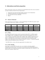
2 - Alternatives and their properties
Before choosing the system to be evaluated, four main DSP-alternatives have been scrutinized
in order to find the one that best fits our requirements:
•
•
•
•
eZdsp F2812 from Spectrum Digital (DSP controller by Texas Instruments)
LabVIEW and hardware from National Instruments
PC with APCI-3110 from Addi-Data
DSpace
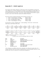
2.1 – Areas of interest
Each system has its own advantages, as well as disadvantages. The table below grants a quick
view of these and how they compare to one another.
System
Price
User friendly Signal levels
Ethernet
eZdsp F2812
LabVIEW
APCI-3110
DSpace
+++
*
---
?
++
?
+++
-+++
+
?
?
+++
+++
+++
Mathworks
integration
?
?
?
+++
2.1.1 - Price
The eZdsp F2812 has the lowest cost by far, priced at less than $470 – the DSP controller
chip, if bought in bulk, is available for less than $20 from Texas Instruments. The APCI3110-card alone costs around $1000 but then you need a fully equipped computer as well to
utilize it, making the price go up quite a bit. LabVIEW comes in a wide range of different
setups, a system that fits our needs should cost approximately $3500 without discount.
DSpace on the other hand is the most expensive alternative of the four – though offering high
quality systems; the $6000 price tag is a bit too big.
* LabVIEW offers a variety of discount opportunities for academic users.
2.1.2 - User friendly
Both DSpace and LabVIEW have great, easy-to-use interfaces featuring graphical
programming and sleek layouts. The solutions from Addi-data and Spectrum Digital don’t
offer the same level of intuitivity, lacking the graphical programming of the competitors. The
Mathworks integration might fix this.
5
2.1.3 - Signal levels
Regarding signal levels, the eZdsp is the only alternative that doesn’t support the standardized
[-10, 10] V by default – however, as part of a previous master thesis, a custom built interface
card has been fitted to the system in order to receive proper signal levels.
2.1.4 - Ethernet
Network connectivity is not of any main concern, though it is a nice feature mastered by
National Instruments. The APCI-3110 is only limited by the features of the PC it’s installed
upon so it should also be regarded as somewhat connected. The eZdsp F2812 on the other
hand – completely lacks this feature, the CPU-chip supports it however – and there are other
DSPs based on this that comes with an Ethernet connection.
2.1.5 - Mathworks integration
MATLAB has specific links for both DSpace and the eZdsp F2812, Code Composer Studio
actually. MATLAB also supports PCs as targets so the APCI-3110 should also be considered
to be somewhat integrated – it is unclear which compiler to use however since none are
included in the bundle, so it should therefore be considered possible but tiresome.
2.2 – The verdict
With all the factors above taken into account, the eZdsp F2812 from Spectrum Digital seems
to be very interesting to evaluate considering the needs and resources of the department.
6
3 - Hardware
In the previous chapter the decision to evaluate the Spectrum Digital eZdsp F2812 was made.
The obvious reasons for choosing the eZdsp is the price and versatile nature of the chip,
should one like to mass produce a product – the DSP-chip from Texas Instruments is available
at a cost that none of the alternatives can hope to rival.
Another reason for choosing this development board is that MATLAB/Simulink has specific
software tools for programming it. How well these will fill our needs will hopefully be
determined during the progression of this report.
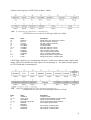
Now, let’s take a look at the features and performance offered by the DSP:
TMS320F2812 by Texas Instruments
Generation:
Clock speed:
Memory:
Pulse Width Modulation signals:
Analog to Digital-Conversion:
Input/Output-pins:
Signal levels:
TMS320F281x Controllers
150 MHz
256 Kb (though expandable up to 1 Mb)
16-channels, space vector capability
16-channels, 12-bit resolution, 80 ns conversion time
Up to 56
[0, 3.3] V, (0-3 V on ADC-pins)
The DSP is fitted to a development board, the eZdsp F2812 from Spectrum Digital, and is
encased in a metal frame together with an interface card constructed as part of the master
thesis mentioned earlier in chapter 2.1.3. The interface card emulates the signal levels of
DSpace – this is of minor importance to this thesis however, since it is the capabilities and
behaviour of the DSP that is of primary concern.
The DSP connects to the host computer via its standard parallel port using a JTAG-interface
(Joint Test Action Group, IEEE 1149.1). The F281x offers real-time JTAG, a feature that is
otherwise missing on other processors of the C2000-series. Real-time JTAG grants the user
the option to modify memory content and peripherals while the processor is still running.
Since we’ll be executing most of our programs through Simulink we won’t be taking
advantage of this feature.
The DSP boasts a total of 56 I/O-pins, most which can have multiple functions assigned by
using flags in registers. Each of the pins has the abilty to function as a standard I/O-pin, that
is, either reading or writing digital data. Some of them, however, can be assigned special
functions like Pulse Width Modulation and Analog to Digital Conversion.
The F2812 handles these special functions using a pair of event managers, EVA and EVB.
The two EVx are identical and offer a range of functions that are especially interesting for
motor control and similar applications since most of these functions concern the PWMmodule.
7
Each event manager is equipped with two independent timers – making it a total of four.
Timers are useful when handling time critical algorithms or adding delays. The timer works
more or less like an “egg clock”, where the timer counts either up or down with a 16-bit value
(which can be defined by the user) and causes an interrupt at a user-specified value.
Also available to each event manager is eight PWM waveforms. They can be generated
simultaneously, six of them as three independent pairs with programmable deadbands. The
DSP outputs PWM signals between [0, 3.3] V – but thanks to a custom built interface card,
the PWM levels are converted to [-15, 15] V instead.
The board is equipped with 16 analog-to-digital conversion-channels. Each channel has a 12bit resolution and a 80 ns conversion delay. The maximum sampling frequency is thus 25
MHz. The input signal must be between [0, 3] V. However, the development board available
at the department is equipped with a custom built interface card making it possible to input
signals in the [-10, 10] V range. Users should note that the digital value is aquired using the
following formula:
⎛ Ana log Input − ADCLO ⎞
DigitalValue = 4095 × ⎜
⎟
3
⎝
⎠
ADCLO is marked GND on the front plate.
Common registers and short explanation of their uses can be found in Appendix C.
8
4 - Software
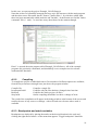
A number of software tools has been used and evaluated for this report, giving the user two
main alternatives when programming – either using Code Composer Studio (CCS) for
traditional coding, or modeling in Simulink. The specific programs and plugins used are:
Code Composer Studio v3.1
MATLAB R2007a
Simulink v6.6
Embedded IDE Link CC v3.0 (Link for Code Composer Studio)
Target Support Package TC2
The Code Composer Studio suite gives the user the choice of writing every row of code in
either c/c+ or assembler language, it is also in charge of the software-to-hardware handling.
Since most of the work in this report have been made through Simulink and automatic c-code
generation using the target- and link-package, CCS has more or less been reduced to a mere
compiler. It is nonetheless quite a powerful tool and a quick guide can be found in the
appendix section of this report.
The CCS v3.1 is shipped with a F2812-emulator – something which might prove itself useful
should the hardware be unavailable. All tested features in this report has however been
performed using the eZdsp F2812 from Spectrum Digital. It should also be noted that CCS is
compatible with a wide range of DSPs should one have second thoughts regarding the
suitability of the current DSP. Regarding the software compatibility CCS v3.1 is compatible
with Embedded Link CC v1.5-v3.0, in other words MATLAB R2006a-R2007a. For newer
releases of MATLAB, CCS v3.3 is required.
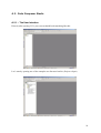
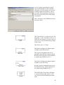
The screenshot below depicts CCS 3.1 in action. To the left the “Project window” with the
open project and all its associated files shown in a standard directory structure. The main part
of the screen is taken up by the “Program window”, allowing the user to view and edit opened
files. The “Output window” in the bottom left corner of the screen relays error messages and
warnings during and after compiling of projects. To the right of the “Output window” lays the
“Watch window”, an extremely useful tool when evaluating models due to the ability watch
variable values in realtime.
9
Screenshot of CCS 3.1
CCS v3.1 comes with a selection of emulators, including a F2812 specific. This is a great
feature considering that the hardware may not always be available. The emulators allow you
to build and even run your programs, though without the features provided by the hardware
such as PWM and ADC.
The Target Support Package and Embedded IDE Link contain Simulink blocks for hardware
setup and hardware specific functions respectively. As noted earlier a guide to these blocks
can be found in the appendix.
It’s when using Simulink that the eZdsp F2812 shows its real strength. An application that
may take hours or even days to write using conventional coding, can easily be implemented in
mere minutes using Simulink standard modeling blocks and a few special blocks for the DSPspecific features. In fact, Simulink simplifies the coding process to the extent that one may
use it with practically no C-code experience at all – it’s not recommended though, since errors
do occur occasionally. We’ll be looking closer at model building in Simulink in the next
chapter.
10
5 - Implementation of a digital relaying algorithm
5.1 – Relays of the past and present
Since the beginning of the 20th century, relays built with electromechanical components have
been used. Reliability and robustness are characteristics for these power electronic artifacts,
and have contributed to their long reign of success.
In the 1960’s, the first investigations into computer relaying was made. The idea at the time
was to integrate all relay applications in one substation into a single computer. This was
necessary due to the expensive nature of computers at the time. Still, the cost, power
consumption and comparatively slow computation speed of the computers couldn’t compete
with conventional relays.
Over the following decade, major advances in computer hardware were made – along with
faster and more efficient algorithms – computer relays performing just as good as their
conventional counterparts were presented in the early 1970’s. During the 1980’s the speed of
processors rose as quick as the manufacturing cost plummeted, which led to the slow
replacement of electromechanical relays by their superior digital brethren. This is a trend that
continues to this day.
11
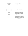
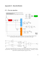
5.2 – The model
To check the suitability of the DSP regarding power electronic applications, a simplified relay
model is constructed. The model contains two DFT-algorithms for signal analysis which is
sufficient for detecting both phase anomalies and amplitude changes.
The model of the implemented relay
A more detailed view of the model as well as the generated C-code can be found in
appendixes D and E. To be able to properly handle three-phase currents, a third DFT should
be added – but since the really important question is if the software is capable, or not, of
reproducing the model in functional C-code only two DFTs are displayed for improved
clarity.
The reader should take the opportunity to note the “F2812 eZdsp”-block, in the lower right
corner, containing the target preferences for the DSP.
The red block (numbered 1) represents the ADC, in this example we’re sampling two
channels and these are demuxed and rerouted into two separate DFTs. (blue and orange in the
picture, depicted by numbers 2 and 3) From the DFTs we may acquire phase angle and
amplitude, using a series of relays we control the three LEDs (using the green Digital Input
block, 4) on the development board to indicate deviations.
The model was built with no warnings or errors and was successfully uploaded to the DSP.
12
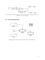
6 - Benchmark
Considering that relays and circuit breakers demand short response times between the actual
error and the moment when the signal has been analysed, a benchmark is of great interest.
The model used for benchmarking
To test the system performance the model above was used. Within the first triggered
subsystem a 1000th order FIR-filter is started as the user pushes one of the buttons on the
hardware’s front plate. At the same time a timer-position is saved, this value is then compared
to the timer-position that is read the moment the calculations are done and the second
subsystem is triggered.
The calculations performed between the two timer-positions are shown in the code segment
shown below:
/* DiscreteFilter Block: '<S2>/Discrete Filter' */
{
int_T i;
const real_T *Amtx = &temp_P.DiscreteFilter_A[0];
real_T *x = &temp_DWork.DiscreteFilter_DSTATE[0];
real_T xtmp = temp_P.Constant_Value;
for (i=998; i>0; i--) {
xtmp += Amtx[i]*x[i];
x[i] = x[i-1];
}
x[0] = xtmp + Amtx[0]*x[0];
}
}
After a vast number of runs, the program consistently returns the timer-difference 540.
13
The system clock frequency of 150MHz is divided by the high speed clock prescaler of 2, and
then divided by the timer control input clock prescaler, which is 128. The resulting frequency
is 0.586MHz.
1
MHz, which is 1.706µs. With 999 multiplications being
0.586
999
performed in the filter loop we get roughly
≈ 1.1MFLOPS .
540 × 1.706µs
Thus, one clock cycle is
According to Texas Instruments, the DSP should be capable of 150 MMACS, Million
Multiply Accumulate Cycles per Second. This is a theoretical peak value, being the product of
the clock speed and the number of MACs, multiply-accumulate operations, that the DSP is
capable of executing per clock cycle.
The result of 1.1 MFLOPS seems a bit low, and the system should be able to perform a lot
better, whether this is due to interrupts or other “hidden” factors are unclear. Nonetheless
should 1+ MFLOPS be more than adequate for some power electronic applications which
depend on a 50 Hz signal.
14
7 - Conclusion
As shown in previous chapters the F2812 performs really well in this type of applications, and
the Link- and Target- package for Simulink makes it a very powerful tool with literally
limitless opportunities.
It’s when using Simulink that the eZdsp F2812 shows its real strength. An application that
may take hours or even days to write using conventional coding, can be easily implemented in
mere minutes using Simulink standard modeling blocks and a few special blocks for the DSPspecific features.
Truly, the ease of transferring a model in Simulink onto the hardware once all obstacles have
been avoided is the systems biggest strength. Included in the appendix of this report is a users
guide and some notes for beginners.
The relay algorithm chosen to emulate the needs of power grid applications was implemented
without any apparent obstacles and once again shows just how user friendly the system is.
The twin DFTs extracted two pairs of amplitudes and phase angles – the break criteria was
governed by a pair of simple relay blocks, band-pass filters, but could just as well been of
derivative nature should one require a more intuitive fault detection.
7.1 - Further work
The F2812 supports Ethernet connectivity, though there already exists custom cards with
connectors already present, it could be interesting to investigate how much work would be
required to add this feature to the eZdsp F2812.
A small LCD-screen would make a great addition to an already excellent platform. Of course,
both this and the Ethernet interface mentioned above should have custom blocks added in
Simulink to maintain the ease of use that characterizes the rest of the system.
15
8 - References
8.1 – Books
[8.1.1]
Computer Relaying for Power Systems, Arun G. Phadke, James S. Thorp, SRP
Ltd., 2000
[8.1.2]
Power System Analysis and Design, J. Duncan Glover, Mulukutla S. Sarma,
Wadsworth Group, 2002
8.2 – DSP Datasheets
[8.2.1]
Data Manual
http://focus.ti.com/lit/ds/symlink/tms320f2812.pdf
[8.2.2]
eZdsp™ F2812 Technical Reference
http://c2000.spectrumdigital.com/ezf2812/docs/ezf2812_techref.pdf
[8.2.3]
Analog-to-Digital Converter (ADC) Reference Guide
http://focus.ti.com/lit/ug/spru060d/spru060d.pdf
[8.2.4]
Event Manager Reference Guide
http://focus.ti.com/lit/ug/spru065e/spru065e.pdf
[8.2.4]
Event Manager Reference Guide
http://focus.ti.com/lit/ug/spru065e/spru065e.pdf
[8.2.5]
C281x C/C++ Header Files and Peripheral Examples
http://focus.ti.com/docs/toolsw/folders/print/sprc097.html
16
Appendix A – A Quick guide to CCS and the hardware
A.1 – Before you start
Basic experience of c/c+ is highly recommended.
Download the example collection SPRC097 from the Texas Instruments website
(www.TI.com). SPRC097 contains a lot of useful programs suitable for the CCS- and DSPnovice, but above all – it contains h- and cmd-files required to access some of the specific
functions of the hardware. Moreover, it includes a guide to the attached programs in pdfformat.
It’s recommended to check out some of the example programs to better understand both CCS
and the DSP. Especially interesting examples (at least in the power electronic point of view)
are these two examples:
adc_soc
ev_pwm
Short introduction to ADC
Deals with the PWM
C++ Primer by Stanley B. Lippman and Josee Lajoie is a great book for reference and
introduction for C-novices.
17
A.2 - Code Composer Studio
A.2.1 – The User Interface
Directly after opening CCS, your screen should look something like this:
Let’s start by opening one of the examples we discussed earlier. (Project->Open)
18
In this case, we open up the project Example_281xEvPwm.pjt.
Note that we have a beautifully arranged directory-style file structure with the main program
and the other source files under the tab "Source", header files (*. h), which are called from
these has been automatically added under the tab "Include". At the bottom we find the "linker
command" files (*. cmd) – we need not worry about those for the moment though.
Here I’ve opened the main program called Example_281xEvPwm.c. All of the example
programs are graciously commented, and should help even a complete novice to better
understand the functions.
A.2.2
Compiling
To compile the project or individual source files a number of different options are available;
from the Project menu or through icons just above the program window.
Compile file
Incremental build
Build all
Stop build
Compiles a single file
Compiles only the files that have changed since last time
Compiles the whole project (all files)
Aborts compiling should the user have a change of heart
The result of the compilation will appear in the debug window at the bottom of the screen and
notifies the user of any errors or warnings - with a file and row-reference where such is
available.
A.2.3 - Breakpoints and watch-variables
Breakpoints are deployed by placing the marker at the desired location in the code and
clicking the right mouse button - on the menu that appears "Toggle breakpoint” should be
19
enabled. (this procedure can also be used for the removal of breakpoints) To review the
deployed breakpoints a command called simply “Breakpoints” is accessible through the
Debug menu." Here you can also add conditions for breakpoints.
Watch variables are invaluable tools when debugging algorithms. They are unfortunately not
updated in real time, but in combination with breakpoints they work very well. There are two
ways to add watch variables, the first and easiest is to simply select the variable you are
interested in directly in the code, right-clicking with the mouse and choosing "Add to watch
window". Alternatively, you can summon the watch window via the View menu or icon that
looks like a pair of glasses. New variables can be manually inserted by double-clicking in the
"Name" column.
A.2.4 – Loading and running programs
When the program is compiled, it’s time to upload it to the DSP. This is done by selecting
"Load program" from the File menu (or alternatively, "Reload program" if you’ve previously
uploaded the same project). You will now find yourself in the current project directory, the
out-file that we are interested in is in the Debug folder. When the program is loaded the
associated assembler code is opened automatically.
Useful commands:
F5:
Shift-F5:
F8:
F10:
Run program
Halt program
Step through the program (useful for reviewing algorithms)
Step over - (as above but never leaves the main-loop)
20
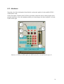
A.3 - Hardware
Note that a lot of the information found in this section only applies for the modified F2812
with interface card.
On the front plate 3 buttons and 3 LEDs are mounted, and below that 16 analog inputs and a
ground connection. Also, the standard parallel port connecting to the host computer is clearly
visible to the right.
The front plate, marked in this picture:
Buttons (1) LEDs (2) ADC-inputs (3) GND-connector (4) and Parallel port (5)
21
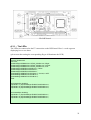
The DSP-board
A.3.1 – The LEDs
The LEDs are connected to the P7-connection on the DSP-board. Here’s a code segment
displaying how to use them:
(please note that setting the corresponding flag to 0 illuminates the LED)
void Init_Diode(void){
EALLOW;
GpioMuxRegs.GPBMUX.bit.C4TRIP_GPIOB13=0; //Right
GpioMuxRegs.GPBMUX.bit.C5TRIP_GPIOB14=0; //Center
GpioMuxRegs.GPBMUX.bit.C6TRIP_GPIOB15=0; //Left
GpioMuxRegs.GPBDIR.bit.GPIOB13=1; //Write
GpioMuxRegs.GPBDIR.bit.GPIOB14=1;
GpioMuxRegs.GPBDIR.bit.GPIOB15=1;
GpioDataRegs.GPBDAT.bit.GPIOB13=1; //0=ON, 1=OFF
GpioDataRegs.GPBDAT.bit.GPIOB14=1;
GpioDataRegs.GPBDAT.bit.GPIOB15=1;
EDIS;
}
void DiodOn(int diodNbr){
if (diodNbr==1) GpioDataRegs.GPBDAT.bit.GPIOB15=0;
if (diodNbr==2) GpioDataRegs.GPBDAT.bit.GPIOB14=0;
if (diodNbr==3) GpioDataRegs.GPBDAT.bit.GPIOB13=0;
}
void DiodOff(int diodNbr){
if (diodNbr==1) GpioDataRegs.GPBDAT.bit.GPIOB15=1;
if (diodNbr==2) GpioDataRegs.GPBDAT.bit.GPIOB14=1;
if (diodNbr==3) GpioDataRegs.GPBDAT.bit.GPIOB13=1;
}
22
A.3.2 – The buttons
The buttons are also connected to the P7-connection and can be used in the following manner:
void Init_Buttons(void){
EALLOW;
GpioMuxRegs.GPAMUX.bit.C1TRIP_GPIOA13=0; //Button B3
GpioMuxRegs.GPAMUX.bit.C2TRIP_GPIOA14=0; //Button B2
GpioMuxRegs.GPAMUX.bit.C3TRIP_GPIOA15=0; //Button B1
GpioMuxRegs.GPADIR.bit.GPIOA13=0; //Read
GpioMuxRegs.GPADIR.bit.GPIOA14=0;
GpioMuxRegs.GPADIR.bit.GPIOA15=0;
//Read BUTTONS ON or OFF:
GpioDataRegs.GPADAT.bit.GPIOA13=1; //Pull-up
GpioDataRegs.GPADAT.bit.GPIOA14=1;
GpioDataRegs.GPADAT.bit.GPIOA15=1;
EDIS;
}
Bool ButtonDown(int buttonNbr){
if (buttonNbr==1 && GpioDataRegs.GPADAT.bit.GPIOA15==0) return TRUE;
if (buttonNbr==2 && GpioDataRegs.GPADAT.bit.GPIOA14==0) return TRUE;
if (buttonNbr==3 && GpioDataRegs.GPADAT.bit.GPIOA13==0) return TRUE;
else return FALSE;
}
A.3.3 – Analog inputs and ADC
The 16 analog inputs are marked A1-A8 and B1-B8. However, this is somewhat misleading,
since their function calls are done using ADCINA0-ADCINA7 (from P9) and ADCINB0ADCINB7 (P5) respectively.
To understand how the ADC works and how to use it, the sample program
Example_281xAdcSoc (found in SPRC097) is highly recommended. The program measures
at analog inputs ADCINA2 and ADCINA3 (ie, A3 and A4 in our case)
Below is a particularly interesting segment of the code:
// Configure ADC
AdcRegs.ADCMAXCONV.all = 0x0001;
// Setup 2 conv's on SEQ1
AdcRegs.ADCCHSELSEQ1.bit.CONV00 = 0x3; // Setup ADCINA3 as 1st SEQ1 conv.
AdcRegs.ADCCHSELSEQ1.bit.CONV01 = 0x2; // Setup ADCINA2 as 2nd SEQ1 conv.
AdcRegs.ADCTRL2.bit.EVA_SOC_SEQ1 = 1; // Enable EVASOC to start SEQ1
AdcRegs.ADCTRL2.bit.INT_ENA_SEQ1 = 1; // Enable SEQ1 interrupt (every EOS)
The first line indicates how many channels that are to be measured, (how much memory to be
freed in order to perform measurements) - if more inputs are desired, the value 0x0001 should
be increased. The next two lines sets which inputs are to be converted. Very logical, replace
0x3 against another value should ADCINA3 not be the preferred input.
23
A.3.4 – Rear connections
The DSP can generate a pulse train with variable period (actually, its duty cycle) - this
method, PWM (Pulse-Width Modulation) is the DSPs main form of signal output.
At the boards back, we have 24 PWM outputs (12 unique), which can be measured by an
oscilloscope. The table below show how the rear connections are placed and denoted.
Rear connections
PWM is best introduced by looking at yet another sample program, Example_281xEvPwm.
Particularly interesting are the two functions init_eva() and init_evb(). In the code segment
below, we take a closer look at init_eva()
void init_eva()
{
// EVA Configure T1PWM, T2PWM, PWM1-PWM6
// Initalize the timers
// Initalize EVA Timer1
EvaRegs.T1PR = 0x0FFF;
// Timer1 period
EvaRegs.T1CMPR = 0x3C00; // Timer1 compare
EvaRegs.T1CNT = 0x0000;
// Timer1 counter
// TMODE = continuous up/down
// Timer enable
// Timer compare enable
EvaRegs.T1CON.all = 0x1042;
24
// Initalize EVA Timer2
EvaRegs.T2PR = 0x03FF;
// Timer2 period
EvaRegs.T2CMPR = 0x03C0; // Timer2 compare
EvaRegs.T2CNT = 0x0000;
// Timer2 counter
// TMODE = continuous up/down
// Timer enable
// Timer compare enable
EvaRegs.T2CON.all = 0x1042;
// Setup T1PWM and T2PWM
// Drive T1/T2 PWM by compare logic
EvaRegs.GPTCONA.bit.TCMPOE = 1;
// Polarity of GP Timer 1 Compare = Active low
EvaRegs.GPTCONA.bit.T1PIN = 1;
// Polarity of GP Timer 2 Compare = Active high
EvaRegs.GPTCONA.bit.T2PIN = 3;
// Enable compare for PWM1-PWM6
EvaRegs.CMPR1 = 0x0C00;
EvaRegs.CMPR2 = 0x3C00;
EvaRegs.CMPR3 = 0xFC00;
// Compare action control. Action that takes place
// on a compare event
// output pin 1 CMPR1 - active high
// output pin 2 CMPR1 - active low
// output pin 3 CMPR2 - active high
// output pin 4 CMPR2 - active low
// output pin 5 CMPR3 - active high
// output pin 6 CMPR3 - active low
EvaRegs.ACTRA.all = 0x0666;
EvaRegs.DBTCONA.all = 0x0000; // Disable deadband
EvaRegs.COMCONA.all = 0xA600;
}
Even if the code is richly commented, some clarifications should be made.
GPTCONA is called bitwise in the code above - an alternative way to set the T1PWM and
T2PWM is to use the command: EvaRegs.GPTCONA.all = 0x0049 (see chap. 5 of Event
Manager Register Guide)
In the same way we could replace EvaRegs.ACTRA.all = 0x0666 with the following lines:
EvaRegs.ACTRA.bit.CMP1ACT1 = 1;
EvaRegs.ACTRA.bit.CMP2ACT0 = 1;
EvaRegs.ACTRA.bit.CMP3ACT1 = 1;
EvaRegs.ACTRA.bit.CMP4ACT0 = 1;
EvaRegs.ACTRA.bit.CMP5ACT1 = 1;
EvaRegs.ACTRA.bit.CMP6ACT0 = 1;
It’s a matter of personal taste since what is lost in space is on the other hand gained in clarity.
25
This concludes the CCS part of the guide, please refer to the literature used in this report for
further information.
26
Appendix B – Simulink blocks
This part of the guide covers some of the new Simulink blocks and how to use them. Basic
knowledge of Simulink and MATLAB is assumed and highly recommended.
The ADC-block handles the setup of
which inputs should have analog-todigital conversion activated.
The user can set sample time as well as
the prefered data type to output. There’s
also options for which modules to
initiate; A and/or B as well as whether
these should be read sequentially or at
the same time.
The number of inputs can be set between
1 and 16 although the block will mux
them together when outputting them so
the user will have to connect a demuxer
when routing the signal.
Unlike CCS, setting up a PWM in
Simulink is incredibly easy. The PWMblock offers a lot of options – for
instance which Event Manager module to
use, the waveform period, whether or not
the waveform should be asymmetric and
of course, which outputs to enable.
27
A lot of options regarding the control
logic and deadband are also available –
giving the user full control over how the
resulting signal should behave. Due to
the nature of the application featured in
this report, this has not been thoroughly
investigated.
Note: All inputs to the PWM-block must
be scalar values.
The Timer-block is a useful tool, be it for
triggering a time dependent task or to
check the time taken to execute a task (as
can be seen in the benchmarking chapter
of this report.
One clock cycle is 1.706µs.
This block configures the digital inputs
available (read: the buttons)
This is pretty straightforward, but it
should be noted that the buttons marked
B1-B3 on the front plate of the hardware
is called using GPIOA bit 15-13.
This block configures the digital outputs
available (read: the LEDs)
It works in pretty much the same way as
the DI-block above. LEDs marked D1-3
are called using GPIOB bit 15-13.
The RTDX, Real Time Data eXchange,
is a great tool that sadly doesn’t work
very well with the Simulink-generated
code.
28
Nonetheless, it has great potential and a
closer look at the example programs
provided by Mathworks is highly
recommended.
Finally, some old acquaintances:
The data type conversion block is
invaluable when switching between
integers, booleans and doubles.
The embedded MATLAB Function
block offers the opportunity to add your
own custom code to the model – and
consequently, the program itself.
Triggered subsystems, as well as
ordinary subsystems are great tools – not
just for signal routing, their block names
show up the c-code as well which greatly
facilitates debugging and general
understanding of the code.
29
Appendix C – Useful registers
The contents of this chapter should be of little interest when using Simulink to generate the
code. Should one ever need to troubleshoot or decide to write segments of code by hand – the
registers shown below are of great interest. The reader should note that this chapter is not to
be considered a full reference guide – but merely a quick explanation of the F2812’s register
structure, a list of some of the most common ones and their functions.
The timer registers include the following: (same principle for timers 2-4)
• Timer 1 Counter Register (T1CNT)
Address 7401h
• Timer 1 Compare Register (T1CMPR)
Address 7402h
• Timer 1 Period Register (T1PR)
Address 7403h
• Timer 1 Control Register (T1CON)
Address 7404h
The first three are pretty straightforward – each containing a 16-bit value. T1CON on the
other hand, is well worth a closer look:
T1CON as seen in the Event Manager Reference Guide
Bit(s)
15:14
13
12−11
10−8
7
6
5−4
3−2
1
0
Name
FREE, SOFT
Reserved
TMODE1−TMODE0
TPS2−TPS0
T2SWT1/T4SWT3
TENABLE
TCLKS(1,0)
TCLD(1,0)
TECMPR
SELT1PR, SELT3PR
Description
Emulation control bits
Reads return zero, writes have no effect.
Count mode selection
Input clock prescaler
Timer enable
Clock source
Timer compare register reload condition
Timer compare enable
Period register select
A lot of options are available to the user by setting the correct flags, the register above for
example, offers the choice of external or internal clocks as well as setting the behaviour of the
internal clock. How to set flags was covered briefly in appendix A.
30
Another useful register is GPTCONA (Address 7400h)
GPTCONA as seen in the Event Manager Reference Guide
Bit(s)
15
14
13
12
11
10−9
8−7
6
5
4
3−2
1−0
Name
Reserved
T2STAT
T1STAT
T2CTRIPE
T1CTRIPE
T2TOADC
T1TOADC
TCMPOE
T2CMPOE
T1CMPOE
T2PIN
T1PIN
Description
Reads return zero; writes have no effect.
GP timer 2 Status. Read only
GP timer 1 Status. Read only
T2CTRIP Enable.
T1CTRIP Enable
Start ADC with timer 2 event
Start ADC with timer 1 event
Timer compare output enable
Timer 2 compare output enable
Timer 1 Compare Output Enable
Polarity of GP timer 2 compare output
Polarity of GP timer 1 compare output
GPTCONA contains a lot of options that will prove useful when capturing data with the ADC
inputs. GPTCONA handles the ADC inputs of event manager A – the same principle applies
to GPTCONB and event manager B.
COMCONA as seen in the Event Manager Reference Guide
Bit(s)
15
14−13
12
11−10
9
8
7
6
5
Name
CENABLE
CLD1, CLD0
SVENABLE
ACTRLD1, ACTRLD0
FCMPOE
PDPINTA
FCMP3OE
FCMP2OE
FCMP1OE
Description
Compare enable
Compare register CMPRx reload condition
Space vector PWM mode enable
Action control register reload condition
Full Compare Output Enable:
Full Compare 3 Output Enable
Full Compare 2 Output Enable:
Full Compare 1 Output Enable:
31
Bit(s)
4−3
2
1
Name
Reserved
C3TRIPE
C2TRIPE
Description
C3TRIP Enable:
C2TRIP Enable:
COMCONA contains settings for the PWM – something that is essential in motor control for
example. The PWM has only been covered very briefly in this report; there is a great
introduction and loads of information regarding both dynamics and general operation in the
Event Manager Reference Guide.
Next up is the compare action control register, ACTRA. Again, this is a register essential to
the PWM and it was mentioned earlier in chapter A.3.4.
ACTRA as seen in the Event Manager Reference Guide
Bit(s)
15
14−13
12
11
10
9
8
7−6
5−4
3−2
1−0
Name
CAPRES
CAP12EN
CAP3EN
Reserved
CAP3TSEL
CAP12TSEL
CAP3TOADC
CAP1EDGE
CAP2EDGE
CAP3EDGE
Reserved
Description
Capture reset. Always reads zero.
Captures 1 and 2 Enable:
Capture 3 Enable:
Reads return zero; writes have no effect.
GP timer selection for capture unit 3.
GP timer selection for capture units 1 and 2.
Capture unit 3 event starts ADC.
Edge detection control for Capture Unit 1.
Edge detection control for Capture Unit 2.
Edge detection control for Capture Unit 3.
Reads return zero; writes have no effect.
While most of the registers deal with event managers and PWM – some are related to the
ADC-inputs instead. For a complete reference of these registers – consult the Analog-toDigital Converter Reference Guide. Let’s take a look at one of the ADC control registers,
ADCTRL1:
32
ADCTRL1 as seen in the Analog-to-Digital Converter Reference Guide
Bit(s)
15
14
13−12
11−8
7
6
5
4
3−0
Name
Reserved
RESET
SUSMOD1−SUSMOD0
ACQ_PS3 −ACQ_PS0
CPS
CONT RUN
SEQ OVRD
SEQ CASC
Reserved
Description
Reads return a zero. Writes have no effect.
ADC module software reset.
Emulation-suspend mode
Acquisition window size.
Core clock prescaler. Applies to HSPCLK.
Continuous run.
Sequencer override. Increases flexibility in continuous run.
Cascaded sequencer operation.
Reads return zero. Writes have no effect.
Among the options for this register is a reset function – when activated it causes the entire
ADC module to reset, and then clears itself afterwards. This could be used to reboot after
break in the relay implementation discussed earlier.
As previously stated – this is just a small part of the available registers – please refer to the
Event Manager Reference Guide and the Analog-to-Digital Converter Reference Guide for
bit-specific actions and other registers.
33
Appendix D – Simulink Models
D.1 – The relay algorithm
This is the main model, notice the ADC block in red, the green Digital Output block
controlling the LEDs and the twin DFTs coloured blue and orange.
The interior of the DFT blocks, expecting sine and cosine signals from the oscillator block
depicted below. The input signal is converted to the frequency domain – outputting a complex
signal whose amplitude and phase trigger the relays.
34
The contents of the oscillator subsystem. A 50 Hz reference signal is on the input side – sineand cosine-waves are outputted.
D.2 – The benchmark model
Making good use of the triggered subsystems, this is the main model view.
35
The first triggered subsystem, triggered by the push of a button – the current timer position is
read and saved – the filter calculation is started and eventually the result is outputted.
The second subsystem – triggered by the result from the previous calculation.
Reads and saves the timer position.
36
Appendix E – C-code
E.1 – The relay algorithm
Code Composer Studio generates all necessary files and directories, I’ve chosen to only
include the main program files, since the rest aren’t program specific.
E.1.1 – TwinDFTs_CCS.c
/*
* TwinDFTs_CCS.c
*
* Real-Time Workshop code generation for Simulink model "TwinDFTs_CCS.mdl".
*
* Model Version
: 1.377
* Real-Time Workshop version : 6.6 (R2007a) 01-Feb-2007
* C source code generated on : Sat Jul 26 15:12:18 2008
*/
#include "TwinDFTs_CCS.h"
#include "TwinDFTs_CCS_private.h"
/* Block signals (auto storage) */
BlockIO_TwinDFTs_CCS TwinDFTs_CCS_B;
/* Block states (auto storage) */
D_Work_TwinDFTs_CCS TwinDFTs_CCS_DWork;
/* Real-time model */
RT_MODEL_TwinDFTs_CCS TwinDFTs_CCS_M_;
RT_MODEL_TwinDFTs_CCS *TwinDFTs_CCS_M = &TwinDFTs_CCS_M_;
/* Model output function */
static void TwinDFTs_CCS_output(int_T tid)
{
/* local block i/o variables */
creal_T rtb_Gain;
creal_T rtb_Product;
creal_T rtb_Conjugat;
real_T rtb_UnitDelay;
real_T rtb_TrigonometricFunction;
real_T rtb_Gain_c[2];
real_T rtb_ComplextoMagnitudeAngle1_o2;
real_T rtb_RelayDFT1;
real_T rtb_RelayDFT2;
real_T rtb_Angle;
real_T rtb_PhaseRelay;
/* UnitDelay: '<S7>/Unit Delay' */
rtb_UnitDelay = TwinDFTs_CCS_DWork.UnitDelay_DSTATE;
/* Trigonometry: '<S7>/Trigonometric Function' */
rtb_TrigonometricFunction = sin(rtb_UnitDelay);
37
/* S-Function Block: <Root>/ADC (c28xadc) */
{
AdcRegs.ADCTRL2.bit.RST_SEQ1 = 0x1;// Sequencer reset
AdcRegs.ADCTRL2.bit.SOC_SEQ1 = 0x1;// Software start of conversion
asm(" nop" );
asm(" nop" );
asm(" nop" );
asm(" nop" );
while (AdcRegs.ADCST.bit.SEQ1_BSY==0x1) {
}
//Wait for Sequencer Busy bit to clear
TwinDFTs_CCS_B.ADC[0] = (AdcRegs.ADCRESULT0) >> 4;
TwinDFTs_CCS_B.ADC[1] = (AdcRegs.ADCRESULT1) >> 4;
AdcRegs.ADCTRL2.bit.RST_SEQ1 = 0x1;// Sequencer reset
AdcRegs.ADCST.bit.INT_SEQ1_CLR = 1;// Clear INT SEQ1 bit
}
/* Gain: '<Root>/Gain' */
rtb_Gain_c[0] = TwinDFTs_CCS_P.Gain_Gain * TwinDFTs_CCS_B.ADC[0];
rtb_Gain_c[1] = TwinDFTs_CCS_P.Gain_Gain * TwinDFTs_CCS_B.ADC[1];
/* Product: '<S1>/Product' */
TwinDFTs_CCS_B.Product = rtb_TrigonometricFunction * rtb_Gain_c[0];
/* DiscreteFilter: '<S1>/Mean of 20 samples' */
rtb_ComplextoMagnitudeAngle1_o2 = TwinDFTs_CCS_P.Meanof20samples_D*
TwinDFTs_CCS_B.Product;
{
int_T nx = 19;
const real_T *x = &TwinDFTs_CCS_DWork.Meanof20samples_DSTATE[0];
const real_T *Cmtx = &TwinDFTs_CCS_P.Meanof20samples_C[0];
while (nx--) {
rtb_ComplextoMagnitudeAngle1_o2 += (*Cmtx) * (*x++);
Cmtx += 1;
}
}
/* Trigonometry: '<S7>/Trigonometric Function1' */
rtb_RelayDFT2 = cos(rtb_UnitDelay);
/* Product: '<S1>/Product1' */
TwinDFTs_CCS_B.Product1 = rtb_Gain_c[0] * rtb_RelayDFT2;
/* DiscreteFilter: '<S1>/Mean of 20 samples1' */
rtb_PhaseRelay = TwinDFTs_CCS_P.Meanof20samples1_D*TwinDFTs_CCS_B.Product1;
{
int_T nx = 19;
const real_T *x = &TwinDFTs_CCS_DWork.Meanof20samples1_DSTATE[0];
const real_T *Cmtx = &TwinDFTs_CCS_P.Meanof20samples1_C[0];
while (nx--) {
rtb_PhaseRelay += (*Cmtx) * (*x++);
Cmtx += 1;
}
}
/* Gain: '<S1>/Gain' incorporates:
* RealImagToComplex: '<S1>/Real-Imag to Complex'
38
*/
rtb_Gain.re = TwinDFTs_CCS_P.Gain_Gain_n * rtb_ComplextoMagnitudeAngle1_o2;
rtb_Gain.im = TwinDFTs_CCS_P.Gain_Gain_n * rtb_PhaseRelay;
/* ComplexToMagnitudeAngle: '<Root>/Complex to Magnitude-Angle' */
rtb_RelayDFT1 = rt_hypot(rtb_Gain.re, rtb_Gain.im);
/* Relay: '<Root>/Relay DFT1'
*
* Regarding '<Root>/Relay DFT1':
* Input0 Data Type: Floating Point real_T
* Output0 Data Type: Floating Point real_T
* On Points Value parameter uses the same data type and scaling as Input0
* Off Points Value parameter uses the same data type and scaling as Input0
* On Output Value parameter uses the same data type and scaling as Output0
* Off Output Value parameter uses the same data type and scaling as Output0
*/
if (rtb_RelayDFT1 >= TwinDFTs_CCS_P.RelayDFT1_OnVal ) {
TwinDFTs_CCS_DWork.RelayDFT1_Mode = TRUE;
} else if (rtb_RelayDFT1 <= TwinDFTs_CCS_P.RelayDFT1_OffVal ) {
TwinDFTs_CCS_DWork.RelayDFT1_Mode = FALSE;
}
rtb_RelayDFT1 = TwinDFTs_CCS_DWork.RelayDFT1_Mode ?
TwinDFTs_CCS_P.RelayDFT1_YOn : TwinDFTs_CCS_P.RelayDFT1_YOff;
/* Product: '<S2>/Product' */
TwinDFTs_CCS_B.Product_j = rtb_TrigonometricFunction * rtb_Gain_c[1];
/* DiscreteFilter: '<S2>/Mean of 20 samples' */
rtb_Angle = TwinDFTs_CCS_P.Meanof20samples_D_l*TwinDFTs_CCS_B.Product_j;
{
int_T nx = 19;
const real_T *x = &TwinDFTs_CCS_DWork.Meanof20samples_DSTATE_p[0];
const real_T *Cmtx = &TwinDFTs_CCS_P.Meanof20samples_C_i[0];
while (nx--) {
rtb_Angle += (*Cmtx) * (*x++);
Cmtx += 1;
}
}
/* Product: '<S2>/Product1' */
TwinDFTs_CCS_B.Product1_l = rtb_Gain_c[1] * rtb_RelayDFT2;
/* DiscreteFilter: '<S2>/Mean of 20 samples1' */
rtb_PhaseRelay = TwinDFTs_CCS_P.Meanof20samples1_D_d*TwinDFTs_CCS_B.Product1_l;
{
int_T nx = 19;
const real_T *x = &TwinDFTs_CCS_DWork.Meanof20samples1_DSTATE_f[0];
const real_T *Cmtx = &TwinDFTs_CCS_P.Meanof20samples1_C_b[0];
while (nx--) {
rtb_PhaseRelay += (*Cmtx) * (*x++);
Cmtx += 1;
}
}
/* Gain: '<S2>/Gain' incorporates:
* RealImagToComplex: '<S2>/Real-Imag to Complex'
39
*/
rtb_Product.re = TwinDFTs_CCS_P.Gain_Gain_m * rtb_Angle;
rtb_Product.im = TwinDFTs_CCS_P.Gain_Gain_m * rtb_PhaseRelay;
/* ComplexToMagnitudeAngle: '<Root>/Complex to Magnitude-Angle1' */
rtb_RelayDFT2 = rt_hypot(rtb_Product.re, rtb_Product.im);
/* Relay: '<Root>/Relay DFT2'
*
* Regarding '<Root>/Relay DFT2':
* Input0 Data Type: Floating Point real_T
* Output0 Data Type: Floating Point real_T
* On Points Value parameter uses the same data type and scaling as Input0
* Off Points Value parameter uses the same data type and scaling as Input0
* On Output Value parameter uses the same data type and scaling as Output0
* Off Output Value parameter uses the same data type and scaling as Output0
*/
if (rtb_RelayDFT2 >= TwinDFTs_CCS_P.RelayDFT2_OnVal ) {
TwinDFTs_CCS_DWork.RelayDFT2_Mode = TRUE;
} else if (rtb_RelayDFT2 <= TwinDFTs_CCS_P.RelayDFT2_OffVal ) {
TwinDFTs_CCS_DWork.RelayDFT2_Mode = FALSE;
}
rtb_RelayDFT2 = TwinDFTs_CCS_DWork.RelayDFT2_Mode ?
TwinDFTs_CCS_P.RelayDFT2_YOn : TwinDFTs_CCS_P.RelayDFT2_YOff;
/* Math: '<Root>/Conjugat' */
/* Operator : conj */
rtb_Conjugat.re = rtb_Product.re;
rtb_Conjugat.im = -rtb_Product.im;
/* Gain: '<S6>/Gain' incorporates:
* ComplexToMagnitudeAngle: '<Root>/Angle'
* Product: '<Root>/Product'
*/
rtb_PhaseRelay = rt_atan2(rtb_Gain.re * rtb_Conjugat.im + rtb_Gain.im *
rtb_Conjugat.re, rtb_Gain.re * rtb_Conjugat.re - rtb_Gain.im *
rtb_Conjugat.im) * TwinDFTs_CCS_P.Gain_Gain_e;
/* Relay: '<Root>/Phase Relay'
*
* Regarding '<Root>/Phase Relay':
* Input0 Data Type: Floating Point real_T
* Output0 Data Type: Floating Point real_T
* On Points Value parameter uses the same data type and scaling as Input0
* Off Points Value parameter uses the same data type and scaling as Input0
* On Output Value parameter uses the same data type and scaling as Output0
* Off Output Value parameter uses the same data type and scaling as Output0
*/
if (rtb_PhaseRelay >= TwinDFTs_CCS_P.PhaseRelay_OnVal ) {
TwinDFTs_CCS_DWork.PhaseRelay_Mode = TRUE;
} else if (rtb_PhaseRelay <= TwinDFTs_CCS_P.PhaseRelay_OffVal ) {
TwinDFTs_CCS_DWork.PhaseRelay_Mode = FALSE;
}
rtb_PhaseRelay = TwinDFTs_CCS_DWork.PhaseRelay_Mode ?
TwinDFTs_CCS_P.PhaseRelay_YOn : TwinDFTs_CCS_P.PhaseRelay_YOff;
/* SignalConversion: '<Root>/TmpHiddenBufferAtDigital OutputInport1' */
40
TwinDFTs_CCS_B.TmpHiddenBufferAtDigitalOutputI[0] = rtb_RelayDFT1;
TwinDFTs_CCS_B.TmpHiddenBufferAtDigitalOutputI[1] = rtb_RelayDFT2;
TwinDFTs_CCS_B.TmpHiddenBufferAtDigitalOutputI[2] = rtb_PhaseRelay;
/* S-Function Block: <Root>/Digital Output (c28xgpio_do) */
{
GpioDataRegs.GPBDAT.bit.GPIOB13 = (boolean_T)
(TwinDFTs_CCS_B.TmpHiddenBufferAtDigitalOutputI[0]);
GpioDataRegs.GPBDAT.bit.GPIOB14 = (boolean_T)
(TwinDFTs_CCS_B.TmpHiddenBufferAtDigitalOutputI[1]);
GpioDataRegs.GPBDAT.bit.GPIOB15 = (boolean_T)
(TwinDFTs_CCS_B.TmpHiddenBufferAtDigitalOutputI[2]);
}
/* RelationalOperator: '<S8>/Relational Operator' incorporates:
* Constant: '<S8>/Constant2'
*/
TwinDFTs_CCS_B.RelationalOperator = (rtb_UnitDelay >
TwinDFTs_CCS_P.Constant2_Value);
/* Switch: '<S8>/Teta < 2*pi' incorporates:
* Constant: '<S8>/Constant2'
* Sum: '<S8>/Sum1'
*/
if (TwinDFTs_CCS_B.RelationalOperator) {
TwinDFTs_CCS_B.Teta2pi = rtb_UnitDelay - TwinDFTs_CCS_P.Constant2_Value;
} else {
TwinDFTs_CCS_B.Teta2pi = rtb_UnitDelay;
}
/* RelationalOperator: '<S8>/Relational Operator1' incorporates:
* Constant: '<S8>/Constant1'
*/
TwinDFTs_CCS_B.RelationalOperator1 = (TwinDFTs_CCS_B.Teta2pi <
TwinDFTs_CCS_P.Constant1_Value_h);
/* Switch: '<S8>/Teta > -2*pi' incorporates:
* Constant: '<S8>/Constant1'
* Sum: '<S8>/Sum2'
*/
if (TwinDFTs_CCS_B.RelationalOperator1) {
TwinDFTs_CCS_B.Teta2pi_k = TwinDFTs_CCS_B.Teta2pi TwinDFTs_CCS_P.Constant1_Value_h;
} else {
TwinDFTs_CCS_B.Teta2pi_k = TwinDFTs_CCS_B.Teta2pi;
}
/* Product: '<S7>/Product' incorporates:
* Constant: '<Root>/Constant1'
* Constant: '<S7>/Constant'
*/
TwinDFTs_CCS_B.Product_b = TwinDFTs_CCS_P.Constant1_Value *
TwinDFTs_CCS_P.Constant_Value;
/* Sum: '<S7>/Sum' */
TwinDFTs_CCS_B.Sum = TwinDFTs_CCS_B.Product_b + TwinDFTs_CCS_B.Teta2pi_k;
UNUSED_PARAMETER(tid);
}
/* Model update function */
41
static void TwinDFTs_CCS_update(int_T tid)
{
/* Update for UnitDelay: '<S7>/Unit Delay' */
TwinDFTs_CCS_DWork.UnitDelay_DSTATE = TwinDFTs_CCS_B.Sum;
/* DiscreteFilter Block: '<S1>/Mean of 20 samples' */
{
int_T i;
const real_T *Amtx = &TwinDFTs_CCS_P.Meanof20samples_A[0];
real_T *x = &TwinDFTs_CCS_DWork.Meanof20samples_DSTATE[0];
real_T xtmp = TwinDFTs_CCS_B.Product;
for (i=18; i>0; i--) {
xtmp += Amtx[i]*x[i];
x[i] = x[i-1];
}
x[0] = xtmp + Amtx[0]*x[0];
}
/* DiscreteFilter Block: '<S1>/Mean of 20 samples1' */
{
int_T i;
const real_T *Amtx = &TwinDFTs_CCS_P.Meanof20samples1_A[0];
real_T *x = &TwinDFTs_CCS_DWork.Meanof20samples1_DSTATE[0];
real_T xtmp = TwinDFTs_CCS_B.Product1;
for (i=18; i>0; i--) {
xtmp += Amtx[i]*x[i];
x[i] = x[i-1];
}
x[0] = xtmp + Amtx[0]*x[0];
}
/* DiscreteFilter Block: '<S2>/Mean of 20 samples' */
{
int_T i;
const real_T *Amtx = &TwinDFTs_CCS_P.Meanof20samples_A_a[0];
real_T *x = &TwinDFTs_CCS_DWork.Meanof20samples_DSTATE_p[0];
real_T xtmp = TwinDFTs_CCS_B.Product_j;
for (i=18; i>0; i--) {
xtmp += Amtx[i]*x[i];
x[i] = x[i-1];
}
x[0] = xtmp + Amtx[0]*x[0];
}
/* DiscreteFilter Block: '<S2>/Mean of 20 samples1' */
{
int_T i;
const real_T *Amtx = &TwinDFTs_CCS_P.Meanof20samples1_A_n[0];
real_T *x = &TwinDFTs_CCS_DWork.Meanof20samples1_DSTATE_f[0];
real_T xtmp = TwinDFTs_CCS_B.Product1_l;
for (i=18; i>0; i--) {
xtmp += Amtx[i]*x[i];
x[i] = x[i-1];
}
x[0] = xtmp + Amtx[0]*x[0];
}
42
/* Update absolute time for base rate */
if (!(++TwinDFTs_CCS_M->Timing.clockTick0))
++TwinDFTs_CCS_M->Timing.clockTickH0;
TwinDFTs_CCS_M->Timing.t[0] = TwinDFTs_CCS_M->Timing.clockTick0 *
TwinDFTs_CCS_M->Timing.stepSize0 + TwinDFTs_CCS_M->Timing.clockTickH0 *
TwinDFTs_CCS_M->Timing.stepSize0 * 4294967296.0;
UNUSED_PARAMETER(tid);
}
/* Model initialize function */
void TwinDFTs_CCS_initialize(boolean_T firstTime)
{
(void)firstTime;
/* Registration code */
/* initialize real-time model */
(void) memset((char_T *)TwinDFTs_CCS_M,0,
sizeof(RT_MODEL_TwinDFTs_CCS));
/* Initialize timing info */
{
int_T *mdlTsMap = TwinDFTs_CCS_M->Timing.sampleTimeTaskIDArray;
mdlTsMap[0] = 0;
TwinDFTs_CCS_M->Timing.sampleTimeTaskIDPtr = (&mdlTsMap[0]);
TwinDFTs_CCS_M->Timing.sampleTimes =
(&TwinDFTs_CCS_M->Timing.sampleTimesArray[0]);
TwinDFTs_CCS_M->Timing.offsetTimes =
(&TwinDFTs_CCS_M->Timing.offsetTimesArray[0]);
/* task periods */
TwinDFTs_CCS_M->Timing.sampleTimes[0] = (0.001);
/* task offsets */
TwinDFTs_CCS_M->Timing.offsetTimes[0] = (0.0);
}
rtmSetTPtr(TwinDFTs_CCS_M, &TwinDFTs_CCS_M->Timing.tArray[0]);
{
int_T *mdlSampleHits = TwinDFTs_CCS_M->Timing.sampleHitArray;
mdlSampleHits[0] = 1;
TwinDFTs_CCS_M->Timing.sampleHits = (&mdlSampleHits[0]);
}
rtmSetTFinal(TwinDFTs_CCS_M, -1);
TwinDFTs_CCS_M->Timing.stepSize0 = 0.001;
TwinDFTs_CCS_M->solverInfoPtr = (&TwinDFTs_CCS_M->solverInfo);
TwinDFTs_CCS_M->Timing.stepSize = (0.001);
rtsiSetFixedStepSize(&TwinDFTs_CCS_M->solverInfo, 0.001);
rtsiSetSolverMode(&TwinDFTs_CCS_M->solverInfo, SOLVER_MODE_SINGLETASKING);
/* block I/O */
TwinDFTs_CCS_M->ModelData.blockIO = ((void *) &TwinDFTs_CCS_B);
(void) memset(((void *) &TwinDFTs_CCS_B),0,
sizeof(BlockIO_TwinDFTs_CCS));
{
int_T i;
void *pVoidBlockIORegion;
43
pVoidBlockIORegion = (void *)(&TwinDFTs_CCS_B.ADC[0]);
for (i = 0; i < 13; i++) {
((real_T*)pVoidBlockIORegion)[i] = 0.0;
}
}
/* parameters */
TwinDFTs_CCS_M->ModelData.defaultParam = ((real_T *) &TwinDFTs_CCS_P);
/* states (dwork) */
TwinDFTs_CCS_M->Work.dwork = ((void *) &TwinDFTs_CCS_DWork);
(void) memset((char_T *) &TwinDFTs_CCS_DWork,0,
sizeof(D_Work_TwinDFTs_CCS));
{
int_T i;
real_T *dwork_ptr = (real_T *) &TwinDFTs_CCS_DWork.UnitDelay_DSTATE;
for (i = 0; i < 77; i++) {
dwork_ptr[i] = 0.0;
}
}
/* initialize non-finites */
rt_InitInfAndNaN(sizeof(real_T));
}
/* Model terminate function */
void TwinDFTs_CCS_terminate(void)
{
/* (no terminate code required) */
}
/*========================================================================*
* Start of GRT compatible call interface
*
*========================================================================*/
void MdlOutputs(int_T tid)
{
TwinDFTs_CCS_output(tid);
}
void MdlUpdate(int_T tid)
{
TwinDFTs_CCS_update(tid);
}
void MdlInitializeSizes(void)
{
TwinDFTs_CCS_M->Sizes.numContStates = (0);/* Number of continuous states */
TwinDFTs_CCS_M->Sizes.numY = (0); /* Number of model outputs */
TwinDFTs_CCS_M->Sizes.numU = (0); /* Number of model inputs */
TwinDFTs_CCS_M->Sizes.sysDirFeedThru = (0);/* The model is not direct feedthrough */
TwinDFTs_CCS_M->Sizes.numSampTimes = (1);/* Number of sample times */
TwinDFTs_CCS_M->Sizes.numBlocks = (42);/* Number of blocks */
TwinDFTs_CCS_M->Sizes.numBlockIO = (12);/* Number of block outputs */
TwinDFTs_CCS_M->Sizes.numBlockPrms = (177);/* Sum of parameter "widths" */
}
void MdlInitializeSampleTimes(void)
{
}
44
void MdlInitialize(void)
{
/* InitializeConditions for UnitDelay: '<S7>/Unit Delay' */
TwinDFTs_CCS_DWork.UnitDelay_DSTATE = TwinDFTs_CCS_P.UnitDelay_X0;
}
void MdlStart(void)
{
InitAdc();
config_ADC_A (1U, 16U, 0U, 0U, 0U);
EALLOW;
GpioMuxRegs.GPBMUX.all &= 8191U;
GpioMuxRegs.GPBDIR.all |= 57344U;
EDIS;
MdlInitialize();
}
RT_MODEL_TwinDFTs_CCS *TwinDFTs_CCS(void)
{
TwinDFTs_CCS_initialize(1);
return TwinDFTs_CCS_M;
}
void MdlTerminate(void)
{
TwinDFTs_CCS_terminate();
}
/*========================================================================*
* End of GRT compatible call interface
*
*========================================================================*/
E.1.2 – TwinDFTs_CCS_main.c
/*
* Real-Time Workshop code generation for Simulink model "TwinDFTs_CCS"
*
* Real-Time Workshop file version
: 6.6 (R2007a) 01-Feb-2007
* Real-Time Workshop file generated on : Sat Jul 26 15:12:18 2008
* C source code generated on
: Sat Jul 26 15:12:18 2008
*
* Description:
* Real-Time Workshop Embedded Coder example single rate main assuming
* no operating system.
*
* Compiler specified defines:
* RT
* MODEL
= TwinDFTs_CCS
* NUMST
= 1 (Number of sample times)
* NCSTATES
= 0 (Number of continuous states)
* TID01EQ
=0
*
(Set to 1 if sample time task id's 0 and 1 have equal rates)
*
* For more information:
* o Real-Time Workshop User's Guide
* o Real-Time Workshop Embedded Coder User's Guide
45
* o Embedded Target for TI C6000 DSP User's Guide
*/
#include "TwinDFTs_CCS.h"
#include "TwinDFTs_CCS_private.h"
#include "rtwtypes.h"
#include "rtmodel.h"
#include "rt_sim.h"
#include "c2000_main.h"
#include "DSP281x_Device.h"
#include "DSP281x_Examples.h"
extern RT_MODEL *MODEL(void);
extern void MdlInitializeSizes(void);
extern void MdlInitializeSampleTimes(void);
extern void MdlStart(void);
extern void MdlOutputs(int_T tid);
extern void MdlUpdate(int_T tid);
extern void MdlTerminate(void);
RT_MODEL *S;
volatile int IsrOverrun = 0;
static boolean_T OverrunFlag = 0;
/* Associating rt_OneStep with a real-time clock or interrupt service routine
* is what makes the generated code "real-time". The function rt_OneStep is
* always associated with the base rate of the model. Subrates are managed
* by the base rate from inside the generated code. Enabling/disabling
* interrupts and floating point context switches are target specific. This
* example code indicates where these should take place relative to executing
* the generated code step function. Overrun behavior should be tailored to
* your application needs. This example simply sets an error status in the
* real-time model and returns from rt_OneStep.
*/
void rt_OneStep(void)
{
real_T tnext;
// Check for overrun. Protect OverrunFlag against
// pre-emption
asm(" SETC INTM");
if (OverrunFlag++) {
IsrOverrun = 1;
OverrunFlag--;
asm(" CLRC INTM");
return;
}
asm(" CLRC INTM");
tnext = rt_SimGetNextSampleHit();
rtsiSetSolverStopTime(rtmGetRTWSolverInfo(S), tnext);
MdlOutputs(0);
MdlUpdate(0);
rt_SimUpdateDiscreteTaskSampleHits(rtmGetNumSampleTimes(S),
rtmGetTimingData(S),
rtmGetSampleHitPtr(S),
rtmGetTPtr(S));
OverrunFlag--;
}
//
46
// Entry point into the code
//
void main(void)
{
volatile boolean_T noErr;
const char_T *status;
init_board();
/************************
* Initialize the model *
************************/
rt_InitInfAndNaN(sizeof(real_T));
S = MODEL();
if (rtmGetErrorStatus(S) != NULL) {
/* Error during model registration */
exit(EXIT_FAILURE);
}
rtmSetTFinal(S, rtInf);
MdlInitializeSizes();
MdlInitializeSampleTimes();
status = rt_SimInitTimingEngine(rtmGetNumSampleTimes(S),
rtmGetStepSize(S),
rtmGetSampleTimePtr(S),
rtmGetOffsetTimePtr(S),
rtmGetSampleHitPtr(S),
rtmGetSampleTimeTaskIDPtr(S),
rtmGetTStart(S),
&rtmGetSimTimeStep(S),
&rtmGetTimingData(S));
if (status != NULL) {
/* Failed to initialize sample time engine */
exit(EXIT_FAILURE);
}
MdlStart();
enable_interrupts();
config_schedulerTimer();
noErr =
rtmGetErrorStatus(TwinDFTs_CCS_M) == NULL;
while (noErr ) {
noErr =
rtmGetErrorStatus(TwinDFTs_CCS_M) == NULL;
}
MdlTerminate();
disable_interrupts();
}
E.1.3 – TwinDFTs_CCS_data.c
/*
* TwinDFTs_CCS_data.c
*
* Real-Time Workshop code generation for Simulink model "TwinDFTs_CCS.mdl".
*
* Model Version
: 1.377
* Real-Time Workshop version : 6.6 (R2007a) 01-Feb-2007
* C source code generated on : Sat Jul 26 15:12:18 2008
47
*/
#include "TwinDFTs_CCS.h"
#include "TwinDFTs_CCS_private.h"
/* Block parameters (auto storage) */
Parameters_TwinDFTs_CCS TwinDFTs_CCS_P = {
0.0,
/* UnitDelay_X0 : '<S7>/Unit Delay'
*/
7.3260073260073260E-004,
/* Gain_Gain : '<Root>/Gain'
*/
/* Meanof20samples_A : '<S1>/Mean of 20 samples'
*/
{ -0.0, -0.0, -0.0, -0.0, -0.0, -0.0, -0.0, -0.0, -0.0, -0.0, -0.0, -0.0, -0.0,
-0.0, -0.0, -0.0, -0.0, -0.0, -0.0 },
/* Meanof20samples_C : '<S1>/Mean of 20 samples'
*/
{ 0.05, 0.05, 0.05, 0.05, 0.05, 0.05, 0.05, 0.05, 0.05, 0.05, 0.05, 0.05, 0.05,
0.05, 0.05, 0.05, 0.05, 0.05, 0.05 },
0.05,
/* Meanof20samples_D : '<S1>/Mean of 20 samples'
*/
/* Meanof20samples1_A : '<S1>/Mean of 20 samples1'
*/
{ -0.0, -0.0, -0.0, -0.0, -0.0, -0.0, -0.0, -0.0, -0.0, -0.0, -0.0, -0.0, -0.0,
-0.0, -0.0, -0.0, -0.0, -0.0, -0.0 },
/* Meanof20samples1_C : '<S1>/Mean of 20 samples1'
*/
{ 0.05, 0.05, 0.05, 0.05, 0.05, 0.05, 0.05, 0.05, 0.05, 0.05, 0.05, 0.05, 0.05,
0.05, 0.05, 0.05, 0.05, 0.05, 0.05 },
0.05,
/* Meanof20samples1_D : '<S1>/Mean of 20 samples1'
*/
1.4142135623730951E+000,
/* Gain_Gain_n : '<S1>/Gain'
*/
5.0,
/* RelayDFT1_OnVal : '<Root>/Relay DFT1'
*/
-5.0,
/* RelayDFT1_OffVal : '<Root>/Relay DFT1'
*/
1.0,
/* RelayDFT1_YOn : '<Root>/Relay DFT1'
*/
0.0,
/* RelayDFT1_YOff : '<Root>/Relay DFT1'
*/
/* Meanof20samples_A_a : '<S2>/Mean of 20 samples'
*/
{ -0.0, -0.0, -0.0, -0.0, -0.0, -0.0, -0.0, -0.0, -0.0, -0.0, -0.0, -0.0, -0.0,
-0.0, -0.0, -0.0, -0.0, -0.0, -0.0 },
/* Meanof20samples_C_i : '<S2>/Mean of 20 samples'
*/
{ 0.05, 0.05, 0.05, 0.05, 0.05, 0.05, 0.05, 0.05, 0.05, 0.05, 0.05, 0.05, 0.05,
0.05, 0.05, 0.05, 0.05, 0.05, 0.05 },
0.05,
/* Meanof20samples_D_l : '<S2>/Mean of 20 samples'
*/
/* Meanof20samples1_A_n : '<S2>/Mean of 20 samples1'
*/
48
{ -0.0, -0.0, -0.0, -0.0, -0.0, -0.0, -0.0, -0.0, -0.0, -0.0, -0.0, -0.0, -0.0,
-0.0, -0.0, -0.0, -0.0, -0.0, -0.0 },
/* Meanof20samples1_C_b : '<S2>/Mean of 20 samples1'
*/
{ 0.05, 0.05, 0.05, 0.05, 0.05, 0.05, 0.05, 0.05, 0.05, 0.05, 0.05, 0.05, 0.05,
0.05, 0.05, 0.05, 0.05, 0.05, 0.05 },
0.05,
/* Meanof20samples1_D_d : '<S2>/Mean of 20 samples1'
*/
1.4142135623730951E+000,
/* Gain_Gain_m : '<S2>/Gain'
*/
5.0,
/* RelayDFT2_OnVal : '<Root>/Relay DFT2'
*/
-5.0,
/* RelayDFT2_OffVal : '<Root>/Relay DFT2'
*/
1.0,
/* RelayDFT2_YOn : '<Root>/Relay DFT2'
*/
0.0,
/* RelayDFT2_YOff : '<Root>/Relay DFT2'
*/
5.7295779513082323E+001,
/* Gain_Gain_e : '<S6>/Gain'
*/
90.0,
/* PhaseRelay_OnVal : '<Root>/Phase Relay'
*/
0.0,
/* PhaseRelay_OffVal : '<Root>/Phase Relay'
*/
1.0,
/* PhaseRelay_YOn : '<Root>/Phase Relay'
*/
0.0,
/* PhaseRelay_YOff : '<Root>/Phase Relay'
*/
50.0,
/* Constant1_Value : '<Root>/Constant1'
*/
6.2831853071795866E-003,
/* Constant_Value : '<S7>/Constant'
*/
-6.2831853071795862E+000,
/* Constant1_Value_h : '<S8>/Constant1'
*/
6.2831853071795862E+000
/* Constant2_Value : '<S8>/Constant2'
*/
};
E.2 – The benchmark model
As stated previously, only program specific source files are included.
E.2.1 – benchmark.c
/*
* benchmark.c
*
* Real-Time Workshop code generation for Simulink model "benchmark.mdl".
*
* Model Version
: 1.43
* Real-Time Workshop version : 6.6 (R2007a) 01-Feb-2007
* C source code generated on : Sat Jul 26 15:51:07 2008
*/
49
#include "benchmark.h"
#include "benchmark_private.h"
/* Block signals (auto storage) */
BlockIO_benchmark benchmark_B;
/* Block states (auto storage) */
D_Work_benchmark benchmark_DWork;
/* Previous zero-crossings (trigger) states */
PrevZCSigStates_benchmark benchmark_PrevZCSigState;
/* Real-time model */
RT_MODEL_benchmark benchmark_M_;
RT_MODEL_benchmark *benchmark_M = &benchmark_M_;
/* Model output function */
static void benchmark_output(int_T tid)
{
/* S-Function Block: <Root>/Digital Input (c28xgpio_di) */
{
benchmark_B.DigitalInput = GpioDataRegs.GPADAT.bit.GPIOA15;
}
if ((benchmark_B.DigitalInput > 0U) &&
(benchmark_PrevZCSigState.TriggeredSubsystem_ZCE == 0L)) {
/* Output and update for trigger system: '<Root>/Triggered Subsystem' */
/* DiscreteFilter: '<S2>/Discrete Filter' incorporates:
* Constant: '<Root>/Constant'
*/
benchmark_B.DiscreteFilter = benchmark_P.DiscreteFilter_D*
benchmark_P.Constant_Value;
{
int_T nx = 999;
const real_T *x = &benchmark_DWork.DiscreteFilter_DSTATE[0];
const real_T *Cmtx = &benchmark_P.DiscreteFilter_C[0];
while (nx--) {
benchmark_B.DiscreteFilter += (*Cmtx) * (*x++);
Cmtx += 1;
}
}
/* S-Function Block: <S2>/Read From Timer (smemsrc) */
{
/* Memory Mapped Input */
const uint16_T *memind = (uint16_T *) 29697U;
benchmark_B.ReadFromTimer = *(uint16_T*)(memind++);
}
/* S-Function Block: <S2>/Write Timer To Memorypos. (smemsnk) */
{
/* Memory Mapped Output */
const uint16_T *memind = (uint16_T *) 2147483711U;
*(uint16_T *)(memind++) = (uint16_T) benchmark_B.ReadFromTimer;
}
/* DiscreteFilter Block: '<S2>/Discrete Filter' */
50
{
int_T i;
const real_T *Amtx = &benchmark_P.DiscreteFilter_A[0];
real_T *x = &benchmark_DWork.DiscreteFilter_DSTATE[0];
real_T xtmp = benchmark_P.Constant_Value;
for (i=998; i>0; i--) {
xtmp += Amtx[i]*x[i];
x[i] = x[i-1];
}
x[0] = xtmp + Amtx[0]*x[0];
}
}
benchmark_PrevZCSigState.TriggeredSubsystem_ZCE = (int32_T)
(benchmark_B.DigitalInput > 0U ? POS_ZCSIG : ZERO_ZCSIG);
if (rt_ZCFcn(RISING_ZERO_CROSSING,
&benchmark_PrevZCSigState.TriggeredSubsystem1_ZCE,
(benchmark_B.DiscreteFilter)) != NO_ZCEVENT) {
/* Output and update for trigger system: '<Root>/Triggered Subsystem1' */
/* S-Function Block: <S3>/Read From Timer2 (smemsrc) */
{
/* Memory Mapped Input */
const uint16_T *memind = (uint16_T *) 29697U;
benchmark_B.ReadFromTimer2 = *(uint16_T*)(memind++);
}
/* S-Function Block: <S3>/Write Timer2 To Memorypos. (smemsnk) */
{
/* Memory Mapped Output */
const uint16_T *memind = (uint16_T *) 2147483711U;
*(uint16_T *)(memind++) = (uint16_T) benchmark_B.ReadFromTimer2;
}
}
UNUSED_PARAMETER(tid);
}
/* Model update function */
static void benchmark_update(int_T tid)
{
/* Update absolute time for base rate */
if (!(++benchmark_M->Timing.clockTick0))
++benchmark_M->Timing.clockTickH0;
benchmark_M->Timing.t[0] = benchmark_M->Timing.clockTick0 *
benchmark_M->Timing.stepSize0 + benchmark_M->Timing.clockTickH0 *
benchmark_M->Timing.stepSize0 * 4294967296.0;
UNUSED_PARAMETER(tid);
}
/* Model initialize function */
void benchmark_initialize(boolean_T firstTime)
{
(void)firstTime;
/* Registration code */
/* initialize real-time model */
(void) memset((char_T *)benchmark_M,0,
sizeof(RT_MODEL_benchmark));
51
/* Initialize timing info */
{
int_T *mdlTsMap = benchmark_M->Timing.sampleTimeTaskIDArray;
mdlTsMap[0] = 0;
benchmark_M->Timing.sampleTimeTaskIDPtr = (&mdlTsMap[0]);
benchmark_M->Timing.sampleTimes = (&benchmark_M->Timing.sampleTimesArray[0]);
benchmark_M->Timing.offsetTimes = (&benchmark_M->Timing.offsetTimesArray[0]);
/* task periods */
benchmark_M->Timing.sampleTimes[0] = (0.001);
/* task offsets */
benchmark_M->Timing.offsetTimes[0] = (0.0);
}
rtmSetTPtr(benchmark_M, &benchmark_M->Timing.tArray[0]);
{
int_T *mdlSampleHits = benchmark_M->Timing.sampleHitArray;
mdlSampleHits[0] = 1;
benchmark_M->Timing.sampleHits = (&mdlSampleHits[0]);
}
rtmSetTFinal(benchmark_M, -1);
benchmark_M->Timing.stepSize0 = 0.001;
benchmark_M->solverInfoPtr = (&benchmark_M->solverInfo);
benchmark_M->Timing.stepSize = (0.001);
rtsiSetFixedStepSize(&benchmark_M->solverInfo, 0.001);
rtsiSetSolverMode(&benchmark_M->solverInfo, SOLVER_MODE_SINGLETASKING);
/* block I/O */
benchmark_M->ModelData.blockIO = ((void *) &benchmark_B);
(void) memset(((void *) &benchmark_B),0,
sizeof(BlockIO_benchmark));
{
((real_T*)&benchmark_B.DiscreteFilter)[0] = 0.0;
}
/* parameters */
benchmark_M->ModelData.defaultParam = ((real_T *) &benchmark_P);
/* states (dwork) */
benchmark_M->Work.dwork = ((void *) &benchmark_DWork);
{
int_T i;
real_T *dwork_ptr = (real_T *) &benchmark_DWork.DiscreteFilter_DSTATE[0];
for (i = 0; i < 999; i++) {
dwork_ptr[i] = 0.0;
}
}
/* initialize non-finites */
rt_InitInfAndNaN(sizeof(real_T));
benchmark_PrevZCSigState.TriggeredSubsystem1_ZCE = UNINITIALIZED_ZCSIG;
benchmark_PrevZCSigState.TriggeredSubsystem_ZCE = POS_ZCSIG;
}
52
/* Model terminate function */
void benchmark_terminate(void)
{
/* (no terminate code required) */
}
/*========================================================================*
* Start of GRT compatible call interface
*
*========================================================================*/
void MdlOutputs(int_T tid)
{
benchmark_output(tid);
}
void MdlUpdate(int_T tid)
{
benchmark_update(tid);
}
void MdlInitializeSizes(void)
{
benchmark_M->Sizes.numContStates = (0);/* Number of continuous states */
benchmark_M->Sizes.numY = (0);
/* Number of model outputs */
benchmark_M->Sizes.numU = (0);
/* Number of model inputs */
benchmark_M->Sizes.sysDirFeedThru = (0);/* The model is not direct feedthrough */
benchmark_M->Sizes.numSampTimes = (1);/* Number of sample times */
benchmark_M->Sizes.numBlocks = (10); /* Number of blocks */
benchmark_M->Sizes.numBlockIO = (4); /* Number of block outputs */
benchmark_M->Sizes.numBlockPrms = (2000);/* Sum of parameter "widths" */
}
void MdlInitializeSampleTimes(void)
{
}
void MdlInitialize(void)
{
}
void MdlStart(void)
{
EALLOW;
GpioMuxRegs.GPAMUX.all &= 32767U;
GpioMuxRegs.GPADIR.all &= 32767U;
EDIS;
/* S-Function Block: <Root>/Timer (c28xevtimer) */
{
configure_timerEV1((unsigned int) 10000U, 5000U, 0, 0, 0, 0);
}
MdlInitialize();
}
RT_MODEL_benchmark *benchmark(void)
{
benchmark_initialize(1);
return benchmark_M;
}
53
void MdlTerminate(void)
{
benchmark_terminate();
}
/*========================================================================*
* End of GRT compatible call interface
*
*========================================================================*/
E.2.2 – benchmark_main.c
/*
* Real-Time Workshop code generation for Simulink model "benchmark"
*
* Real-Time Workshop file version
: 6.6 (R2007a) 01-Feb-2007
* Real-Time Workshop file generated on : Sat Jul 26 15:51:07 2008
* C source code generated on
: Sat Jul 26 15:51:07 2008
*
* Description:
* Real-Time Workshop Embedded Coder example single rate main assuming
* no operating system.
*
* Compiler specified defines:
* RT
* MODEL
= benchmark
* NUMST
= 1 (Number of sample times)
* NCSTATES
= 0 (Number of continuous states)
* TID01EQ
=0
*
(Set to 1 if sample time task id's 0 and 1 have equal rates)
*
* For more information:
* o Real-Time Workshop User's Guide
* o Real-Time Workshop Embedded Coder User's Guide
* o Embedded Target for TI C6000 DSP User's Guide
*/
#include "benchmark.h"
#include "benchmark_private.h"
#include "rtwtypes.h"
#include "rtmodel.h"
#include "rt_sim.h"
#include "c2000_main.h"
#include "DSP281x_Device.h"
#include "DSP281x_Examples.h"
extern RT_MODEL *MODEL(void);
extern void MdlInitializeSizes(void);
extern void MdlInitializeSampleTimes(void);
extern void MdlStart(void);
extern void MdlOutputs(int_T tid);
extern void MdlUpdate(int_T tid);
extern void MdlTerminate(void);
RT_MODEL *S;
volatile int IsrOverrun = 0;
static boolean_T OverrunFlag = 0;
/* Associating rt_OneStep with a real-time clock or interrupt service routine
54
* is what makes the generated code "real-time". The function rt_OneStep is
* always associated with the base rate of the model. Subrates are managed
* by the base rate from inside the generated code. Enabling/disabling
* interrupts and floating point context switches are target specific. This
* example code indicates where these should take place relative to executing
* the generated code step function. Overrun behavior should be tailored to
* your application needs. This example simply sets an error status in the
* real-time model and returns from rt_OneStep.
*/
void rt_OneStep(void)
{
real_T tnext;
// Check for overrun. Protect OverrunFlag against
// pre-emption
asm(" SETC INTM");
if (OverrunFlag++) {
IsrOverrun = 1;
OverrunFlag--;
asm(" CLRC INTM");
return;
}
asm(" CLRC INTM");
tnext = rt_SimGetNextSampleHit();
rtsiSetSolverStopTime(rtmGetRTWSolverInfo(S), tnext);
MdlOutputs(0);
MdlUpdate(0);
rt_SimUpdateDiscreteTaskSampleHits(rtmGetNumSampleTimes(S),
rtmGetTimingData(S),
rtmGetSampleHitPtr(S),
rtmGetTPtr(S));
OverrunFlag--;
}
//
// Entry point into the code
//
void main(void)
{
volatile boolean_T noErr;
const char_T *status;
init_board();
/************************
* Initialize the model *
************************/
rt_InitInfAndNaN(sizeof(real_T));
S = MODEL();
if (rtmGetErrorStatus(S) != NULL) {
/* Error during model registration */
exit(EXIT_FAILURE);
}
rtmSetTFinal(S, rtInf);
MdlInitializeSizes();
MdlInitializeSampleTimes();
status = rt_SimInitTimingEngine(rtmGetNumSampleTimes(S),
rtmGetStepSize(S),
rtmGetSampleTimePtr(S),
55
rtmGetOffsetTimePtr(S),
rtmGetSampleHitPtr(S),
rtmGetSampleTimeTaskIDPtr(S),
rtmGetTStart(S),
&rtmGetSimTimeStep(S),
&rtmGetTimingData(S));
if (status != NULL) {
/* Failed to initialize sample time engine */
exit(EXIT_FAILURE);
}
MdlStart();
enable_interrupts();
config_schedulerTimer();
noErr =
rtmGetErrorStatus(benchmark_M) == NULL;
while (noErr ) {
noErr =
rtmGetErrorStatus(benchmark_M) == NULL;
}
MdlTerminate();
disable_interrupts();
}
E.2.3 – benchmark_data.c
/*
* benchmark_data.c
*
* Real-Time Workshop code generation for Simulink model "benchmark.mdl".
*
* Model Version
: 1.43
* Real-Time Workshop version : 6.6 (R2007a) 01-Feb-2007
* C source code generated on : Sat Jul 26 15:51:07 2008
*/
#include "benchmark.h"
#include "benchmark_private.h"
/* Block parameters (auto storage) */
Parameters_benchmark benchmark_P = {
8.1472368639317894E-001,
{ contains the 1000th order vector used by the FIR-filter, removed from this report to the great relief of
the rainforest },
1.1040062944571298E+000
};
56