1
SDFlash Serial v3.1 March 28, 2007
TMS320F28xx SDFlash Serial RS232
Flash Programming Reference Guide
1 of 37
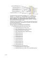
Table of Contents
Revision History......................................................................................................................................3
Limitations and Assumptions................................................................................................................4
Installation Instructions .........................................................................................................................5
Using SDFlash Serial............................................................................................................................10
Rebuilding the SDFlash Serial Files....................................................................................................21
Troubleshooting Tips ...........................................................................................................................31
References.............................................................................................................................................32
Appendix A: Customizing SDFlash Serial for User Applications.....................................................33
2 of 37
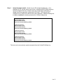
Revision History
v3.1: March 28, 2007. (D. Alter)
- Added support for F28044 using F2804x Flash API algorithms v1.00.
- Added support for F28016 and F28015 using F2801x Flash API algorithms v1.00.
- Added support for F2809 using F2809 Flash API algorithms v1.00.
- Added support for F2802 and F2802-60 using F280x Flash API algorithms v3.02.
- Added support for F2801-60 using F280x Flash API algorithms v3.02.
- Upgraded F2808, F2806, and F2801 support to use F280x Flash API algorithms v3.02.
- Modified the code security unlocking routine to overwrite the downloaded passwords
located in RAM after unlocking the CSM. This applies to all devices.
- Added support for 115200, 4800, 2400, and 1200 baud.
- Added Appendix A that describes SDFlash Serial customization. (C. Peng)
v3.0: September 01, 2005. (D. Alter)
- Added support for F2808, F2806, F2801 using F280x Flash API algorithms v3.00.
- Upgraded F281x API Flash algorithms to v2.10.
- Removed SDFlash executable from bundle.
- Removed Win32 console test program from bundle.
- Consolidated all documentation files into this document
- Fixed linker command file for F281x algorithm build to properly include all .obj files.
- Adjusted descriptions and default values for the ERASE TIMEOUT, PROGRAM
TIMEOUT, and VERIFY TIMEOUT SDFlash project options.
- Added use of Erase User Options #4 and Programming User Options #4 to specify the
Host PC loop retry for erase and programming acknowledgement.
v2.2: October 15, 2004. Original release.
- Support for F2812, F2811, F2810 using F281x Flash API algorithms v1.00.
3 of 37
Limitations and Assumptions
The SDFlash RS232 Serial patch is provided by Spectrum Digital and Texas Instruments
as an “as is” proof of concept example of serial programming for the F28xxx flash DSPs.
The utility as well as the source code is provided as is, without any technical support.
The patch requires use of SDFlash v1.60 or later. These versions of SDFlash support a
generic communications interface that is used to communicate over the RS232 serial link.
All of the source code, project files, and documentation needed to build the .dll files for
SDFlash (e.g., F281xRS232Flash.dll and F280xRS232Flash.dll), the flash programming
DSP download F28yyySerialFlash.out (e.g., F2812SerialFlash.out for F2812 device), and
the code security password match flow DSP download (e.g., F28xxPasswordMF.out) are
available in the following directories:
TMS320F281x devices: <SDFlash_install_dir>\sdflash\mydrivers\DSP281x_v3_1
TMS320F280x devices: <SDFlash_install_dir>\sdflash\mydrivers\DSP280x_v3_1
TMS320F2801x devices: <SDFlash_install_dir>\sdflash\mydrivers\DSP2801x_v3_1
TMS320F2804x devices: <SDFlash_install_dir>\sdflash\mydrivers\DSP2804x_v3_1
The v3.1 SDFlash Serial utility supports the following devices:
TMS320F281x devices: F2812, F2811, F2810
TMS320F280x devices: F2809, F2808, F2806, F2802, F2802-60, F2801, F2801-60
TMS320F2801x devices: F28015, F28016
TMS320F2804x devices: F28044
The SDFlash driver files F281xRS232Flash.dll (for all F281x devices) and
F280xRS232Flash.dll (for all F280x, F2801x, and F2804x devices) were built using
Microsoft Visual C++ v6.00. The flash programming DSP downloads
F28yyySerialFlash.out and the code security password match flow DSP download
F28xxPasswordMF.out (for all F280x, F2801x, and F2804x devices) were built using
Code Composer Studio v3.3 with C28xx C compiler v4.1.3.
This document assumes the reader has some familiarity with the following:
−
SDFlash v1.60 or later for JTAG programming of the F28xxx family.
−
The “TMS320F281x Flash API” (SPRC125), the “TMSF280x Flash API” (SPRC193) ,
the “TMS320F2801x Flash API” (SPRC327), or the “TMS320F2804x Flash API”
(SPRC325) available on TI’s website, http://www.ti.com
Code Composer Studio is a trademark of Texas Instruments Incorporated.
4 of 37
Installation Instructions
Step 1.
Install SDFlash V1.60 or higher.
In version 1.60 and above Spectrum Digital exposed a generic interface that can
support programming via non-JTAG interfaces. The latest SDFlash can be
downloaded from the Spectrum Digital website.
–
Go to www.spectrumdigital.com and register, or login if you have previously
registered. The login button is at the top right of the webpage.
–
Click “Drivers and Config Utilities”
–
Click “C2000 Products” on the list on the left-hand side of the screen
–
Click “Utilities” on the list on the left-hand side of the screen.
–
Click “Install/Download” for the SDFlash utility. This will open the following
webpage:
http://emulators.spectrumdigital.com/utilities/sdflash/
–
Step 2.
Download and install on your PC the latest SDFlash utility (at least v1.60).
Install the SDFlash algorithms for F28xxx flash programming via an RS232
serial link.
–
Go to www.spectrumdigital.com and register, or login if you have previously
registered. The login button is at the top right of the webpage.
–
Click “Drivers and Config Utilities”
–
Click “C2000 Products” on the list on the left-hand side of the screen
–
Click “Utilities” on the list on the left-hand side of the screen.
–
Click “Install/Download” for the SDFlash utility. This will open the following
webpage:
http://emulators.spectrumdigital.com/utilities/sdflash/
–
Download the latest SDFlash algorithms for F28xxx flash programming via an
RS232 serial link.
–
It is recommended to install the patch in the root directory of your SDFlash
installation. For example, if SDFlash is installed in
C:\CCStudio_v3.1\specdig\sdflash, unzip the patch in the
C:\CCStudio_v3.1\specdig\sdflash. This will create five new sub-directories under
mydrivers\, and one new sub-directory under myprojects\ as follows:
5 of 37
mydrivers\DSP280x_60_v3_1
mydrivers\DSP280x_v3_1
mydrivers\DSP281x_v3_1
mydrivers\DSP2801x_v3_1
mydrivers\DSP2804x_v3_1
myprojects\sdf28xx_v3_1_serial
−
The sdflash\mydrivers\ sub-directories DSP280x_60_v3_1, DSP280x_v3_1,
DSP281x_v3_1, DSP2801x_v3_1, and DSP2804x_v3_1 contain the RS232
interface example code for F280x-60, F280x, F281x, F2801x, and F2804x
devices, respectively. This code is supplied as an as-is example of how to
perform programming over the RS232 communications channel. This sample
code is provided without technical support.
−
The directory myprojects\sdf28xx_v3_1_serial contains all of the files specific to
executing serial programming. Each flash device currently in the F28xxx family
has it’s own specific sub directory.
The files required to use SDFlash over a serial link are:
•
The SDFlash Serial project file for the device in use:
F2801SerialFlash.sdp (for F2801 device)
F2801_60SerialFlash.sdp (for F2801-60 device)
F2802SerialFlash.sdp (for F2802 device)
F2802_60SerialFlash.sdp (for F2802-60 device)
F2806SerialFlash.sdp
F2808SerialFlash.sdp
F2809SerialFlash.sdp
F2810SerialFlash.sdp
F2811SerialFlash.sdp
F2812SerialFlash.sdp
F28015SerialFlash.sdp
F28016SerialFlash.sdp
F28044SerialFlash.sdp
•
The SDFlash driver file for the device in use:
F281xRS232Flash.dll (for F281x devices)
F280xRS232Flash.dll (for F280x, F2801x, and F2804x devices)
6 of 37
•
The SDFlash Serial flash algorithm file for the device in use:
F2801SerialFlash.out (for F2801 device)
F2801_60SerialFlash.out (for F2801-60 device)
F2802SerialFlash.out (for F2802 device)
F2802_60SerialFlash.out (for F2802-60 device)
F2806SerialFlash.out
F2808SerialFlash.out
F2809SerialFlash.out
F2810SerialFlash.out
F2811SerialFlash.out
F2812SerialFlash.out
F28015SerialFlash.out
F28016SerialFlash.out
F28044SerialFlash.out
•
The code security password match flow file (applies to F280x, F2801x,
and F2804x devices only):
F28xxPasswordMF.out
•
The CCS board.dat file. The contents of this file is not actually used, but
rather is needed to satisfy a project option in SDFlash.
ccBrd028x.dat
•
The sdopts.cfg setup parameters.
AddToSdOpts.cfg
•
The .out file containing the user code/data that is to be programmed into
the DSP flash. This file is produced from the user’s source code by the
code generation tools in Code Composer Studio. For test purposes, a
sample .out file is provided for each device that will load each flash
location with a value equal to the least-significant 16 bits of the address.
For example, address 0x3F7123 in flash will be programmed with the
value 0x7123. The code security password locations at addresses
0x3F7FF8 – 0x3F7FFF have been deliberately left unprogrammed (i.e.,
they will be left as 0xFFFF, which are dummy passwords). The sample
.out files are:
7 of 37
F2801FlashTest.out (for both F2801 and F2801-60)
F2802FlashTest.out (for both F2802 and F2802-60)
F2806FlashTest.out
F2808FlashTest.out
F2809FlashTest.out
F2810FlashTest.out
F2811FlashTest.out
F2812FlashTest.out
F28015FlashTest.out
F28016FlashTest.out
F28044FlashTest.out
Step 3.
Modify and rebuild the SDFlash Serial algorithm file, if necessary (i.e., file
F28yyySerialFlash.out, where yyy is specific to the device you are using). The
SDFlash v3.1 serial algorithm software is configured for the following:
–
Flash API versions:
–
F280x flash API v3.02
–
F281x flash API v2.10 (requires F281x silicon revision C or later)
–
F2801x flash API v1.00
–
F2804x flash API v1.00
–
For F281x: A crystal/oscillator for the DSP of 30 MHz. This is because the
software will configure the DSP for PLL = x10/2, and the flash API algorithms are
configured for 150 MHz operation.
–
For F280x and F2804x: A crystal/oscillator for the DSP of 20 MHz. This is
because the software will configure the DSP for PLL = x10/2, and the flash API
algorithms are configured for 100 MHz operation.
–
For F280x-60 and F2801x: A crystal/oscillator for the DSP of 20 MHz. This is
because the software will configure the DSP for PLL = x10/2, and the flash API
algorithms are configured for 60 MHz operation.
–
All code security passwords assumed to be erased (0xFFFF).
If your system does not meet the above configuration, you must make changes
to the SDFlash Serial algorithm file and rebuild it. See the section “Rebuilding
the SDFlash Serial Flash Algorithm File” later in this document for information
on rebuilding this file.
IMPORTANT: It is strongly recommended that the Toggle Test first be run on your
board to confirm that the flash algorithms are configured properly for your system.
See the section “Using SDFlash Serial,” Step 6, Erase Tab options, User Options 2
for information on the Toggle Test.
8 of 37
Step 4.
Setup the sdopts.cfg file. Search on your PC for the file sdopts.cfg. On a
Windows XP PC, this file will be found in the C:\WINDOWS\SYSTEM32 directory.
Spectrum Digital tools store emulator setup and configuration information in
sdopts.cfg which is generally configured by SDConfig. SDConfig will NOT
configure a non-JTAG tool so this has to be done manually. Add the following text
to sdopts.cfg before the existing comment line "# End of sdopts.cfg”.
[EmulatorId=C1]
EmuPortAddr=0xC1
EmuPortMode=RS232
EmuProductName=SERIAL_FLASH
[EmulatorId=C2]
EmuPortAddr=0xC2
EmuPortMode=RS232
EmuProductName=SERIAL_FLASH
[EmulatorId=C3]
EmuPortAddr=0xC3
EmuPortMode=RS232
EmuProductName=SERIAL_FLASH
[EmulatorId=C4]
EmuPortAddr=0xC4
EmuPortMode=RS232
EmuProductName=SERIAL_FLASH
This text can be conveniently copied and pasted from the file AddToSdOpts.cfg.
9 of 37
Using SDFlash Serial
Step 1.
Connect a serial cable between the DSP serial port (SCI-A) and the host PC.
The connection must be made through a RS232 transceiver. Note that the
eZdspF2808 and eZdspF28044 development boards do come equipped with this
transceiver, while the eZdspF2812 development board does not.
Step 2.
Set the F28xxx device for boot to SCI-A serial bootload. This entails having
specific GPIO pins high/low at device reset. The eZdsp boards have jumpers or
dip switches that allow one to configure the boot mode (see the user’s manual for
the eZdsp you are using for details). On your own target board, you will need to
make arrangements to configure the boot mode, if necessary. The following two
tables show the GPIO pin settings needed to configure the boot modes.
For F280x and F2801x devices, configure the GPIO according to the following boot
mode table (excerpt from the TMS320F2809/2808/2806/2802/2801/28015/28016
datasheet, SPRS230):
eZdsp is a trademark of Spectrum Digital Incorporated.
10 of 37
For F281x devices, configure the GPIO according to the following boot mode table
(excerpt from the TMS320F2812/2811/2810 datasheet, SPRS174):
For F2804x devices, configure the GPIO according to the following boot mode table
(excerpt from the TMS320F28044 datasheet, SPRS357):
NOTE: When configuring the bootmode, the SCITXDA must be pulled down
through a resistor so that the F28xx can still drive the pin once the bootload
process begins.
Step 3.
If programming the F2812, make sure that the XMP/MCn pin is pulled low to
access the boot ROM. On all other devices (without an XMIF), this signal is tied
low internally such that the boot ROM is always active.
Step 4.
Disconnect any JTAG emulator that may be connected to the DSP board,
such as a XDS510PP+ emulator. An emulator connected to the JTAG port may
hold the device in reset and thus the bootloader will not start when the device is
reset.
11 of 37
Step 5.
Start SDFlash and load the appropriate project file. This will be one of the
following:
myprojects\sdf28xx_v3_1_serial\f2812\F2801SerialFlash.sdp
myprojects\sdf28xx_v3_1_serial\f2811\F2801_60SerialFlash.sdp
myprojects\sdf28xx_v3_1_serial\f2810\F2802SerialFlash.sdp
myprojects\sdf28xx_v3_1_serial\f2808\F2802_60SerialFlash.sdp
myprojects\sdf28xx_v3_1_serial\f2806\F2806SerialFlash.sdp
myprojects\sdf28xx_v3_1_serial\f2801\F2808SerialFlash.sdp
myprojects\sdf28xx_v3_1_serial\f2801\F2809SerialFlash.sdp
myprojects\sdf28xx_v3_1_serial\f2801\F2810SerialFlash.sdp
myprojects\sdf28xx_v3_1_serial\f2801\F2811SerialFlash.sdp
myprojects\sdf28xx_v3_1_serial\f2801\F2812SerialFlash.sdp
myprojects\sdf28xx_v3_1_serial\f2801\F28015SerialFlash.sdp
myprojects\sdf28xx_v3_1_serial\f2801\F28016SerialFlash.sdp
myprojects\sdf28xx_v3_1_serial\f2801\F28044SerialFlash.sdp
Step 6.
Modify the SDFlash project options (if necessary) to locate the various
elements such as the device driver, algorithm file and flash data file. The
directory paths to these files assume the SDFlash is installed in the
C:\CCStudio_v3.3\specdig\sdflash directory. To change any of the directory paths
or project settings from their default values, open the project settings dialog box:
Project->Settings. The project options that follow are specific to the SDFlash
Serial Patch.
IMPORTANT
This is a very important step. If you did not install the SDFlash Serial utility in the
default directory of C:\CCStudio_v3.3\specdig\sdflash, then YOU MUST modify the
file paths in the SDFlash project. Be sure that you check each tab in the project
options. There are multiple places that the file paths are specified. If the wrong
paths are specified, SDFlash Serial may simply report a failure to connect to the DSP
via the serial link, rather than telling you that your project option paths are incorrect.
12 of 37
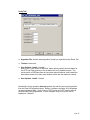
Target Tab: (image shown for F2808 device)
Driver: This must point to either F281xRS232Flash.dll (for F281x devices) or to
F280xRS232Flash.dll (for F280x, F2801x, and F2804x devices).
Emulator Address/ID: This is the COM port on your PC that you are using to
connect to the DSP. If COM1, COM2, COM3 and COM4 do not appear as
options, modify the sdopts.cfg file as described previously in step 4.
Board file: Leave as ccBrd028x.dat
Processor name: Leave as cpu_0
13 of 37
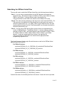
Erase Tab: (image shown for F2808 device)
Algorithm File: use the appropriate file for your device:
myprojects\sdf28xx_v3_1_serial\f2801\F2801SerialFlash.out
myprojects\sdf28xx_v3_1_serial\f2806\F2801_60SerialFlash.out
myprojects\sdf28xx_v3_1_serial\f2806\F2802SerialFlash.out
myprojects\sdf28xx_v3_1_serial\f2806\F2802_60SerialFlash.out
myprojects\sdf28xx_v3_1_serial\f2806\F2806SerialFlash.out
myprojects\sdf28xx_v3_1_serial\f2808\F2808SerialFlash.out
myprojects\sdf28xx_v3_1_serial\f2806\F2809SerialFlash.out
myprojects\sdf28xx_v3_1_serial\f2810\F2810SerialFlash.out
myprojects\sdf28xx_v3_1_serial\f2811\F2811SerialFlash.out
myprojects\sdf28xx_v3_1_serial\f2812\F2812SerialFlash.out
myprojects\sdf28xx_v3_1_serial\f2806\F28015SerialFlash.out
myprojects\sdf28xx_v3_1_serial\f2806\F28016SerialFlash.out
myprojects\sdf28xx_v3_1_serial\f2806\F28044SerialFlash.out
14 of 37
Timeout: This can be left as 0. This value specifies the amount of time per flash
sector (in 10’s of milliseconds) that the host PC waits after sending the DSP an
erase command before it checks for an acknowledge. This option has been
superseded by Erase User Options #4. See the description for Erase User
Options #4 below for more information.
User Options 1: Sector Mask for erase. Default value is set to erase all sectors.
Set Bit 0 = erase Sector A
Set Bit 1 = erase Sector B
...
For example:
000f will erase all 4 sectors in a F2808 device
0001 will erase only sector A in a F2801 device
001f will erase all 5 sectors in a F2810 device
03ff will erase all 10 sectors in a F2812 device
User Options 2: Toggle Test pin select. The toggle test toggles a selected pin
at a known frequency in order to confirm proper configuration of the flash
programming algorithms. While the test runs, monitor the selected pin using an
oscilloscope. If the algorithms are configured correctly for your CPU rate then
the pin will toggle near 10kHz (100µS +/- 10µS cycle time). If the pin is toggling
at a different rate, then the algorithms are not configured correctly. The pin
selection is made as follows:
For F281x devices:
Leave User Options 2 blank or 0000 for normal operation. To run the toggle
test, set User Option 2 to a value of 0001 to 0005, per the below table to select
the desired pin that will toggle. This will invoke the toggle test instead of the
erase operation, and SDFlash will harmlessly timeout eventually. The user can
click Stop to halt the toggle test sooner. Note that the DSP continues to run the
Toggle test even after SDFlash has timed out.
Blank
0000
0001
0002
0003
0004
0005
0006-FFFF
Test not run
Test not run
GPIOF14_XF
GPIOA0_PWM1
Test not run
GPIOG4_SCITXDB
GPIOF12_MDXA
Test not run
For F280x, F2801x, and F2804x devices:
Set User Options 2 to a number greater than 0022 for normal operation (e.g.,
default is 0099). To run the toggle test, set User Options 2 to a hexadecimal
value equal to the GPIO pin number that you want to toggle. For example:
0000 toggles GPIO0
0001 toggles GPIO1
...
0010 toggles GPIO16
...
0022 toggles GPIO34
Greater than 0022 toggle test does not run.
15 of 37
This will invoke the toggle test instead of the erase operation, and SDFlash will
harmlessly timeout eventually. The user can click Stop to halt the toggle test
sooner. Note that the DSP continues to run the Toggle test even after SDFlash
has timed out.
If the toggling does not occur at the expected frequency, changes need to be
made to the SDFlash Serial algorithm file, per the previous step 3.
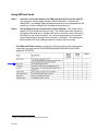
User Options 3: Default Autobaud setting. Although this is on the Erase tab, it
applies to all operations (toggle test, Erase, Program and Verify). Enter a
number 0001 - 0004 that sets the default baud rate that SDFlash will attempt to
autobaud lock with the DSP boot loader:
0001
0002
0003
0004
0005
0006
0007
0008
Other
57600 baud
38400 baud
19200 baud (Default)
9600 baud
4800 baud
2400 baud
1200 baud
115200 baud
38400 baud
Due to hardware, connectors, transceiver, PC UART, etc., you may need to
lower the autobaud rate in order to successfully autobaud lock with the DSP.
Tabulated below are very rough estimates on the expected programming times
at various baud rates:
16 of 37
Baud
Rate
Time to
‘Connect’
Time to
Transfer
1 KB of
flash data
Minimum
Total
Time to
Program
32 KB
Minimum
Total
Time to
Program
64 KB
Minimum
Total
Time to
Program
128 KB
115200
12 sec
96 ms
15 sec
18 sec
24 sec
57600
13 sec
193 ms
19 sec
25 sec
38 sec
38400
15 sec
290 ms
24 sec
34 sec
52 sec
19200
28 sec
580 ms
47 sec
1.1 min
1.7 min
9600
52 sec
1.2 sec
1.5 min
2.2 min
3.4 min
4800
1.7 min
2.3 sec
2.9 min
4.1 min
6.6 min
2400
3.3 min
4.6 sec
5.8 min
8.2 min
13 min
1200
6.5 min
9.3 sec
12 min
17 min
26 min
In the table, the Time to ‘Connect’ is how long SDFlash Serial will display the
“Connect...” message. This portion of the programming involves downloading
the flash programming algorithms and kernel to the DSP. There is some
inefficiency here having to do with single byte transmission delay times
inherent to the serial port drivers on a Windows PC. After this phase, the
Erase phase will be entered, followed by the Programming phase. The Erase
phase does not involve further data transfer from the host PC, and will occur
relatively quickly. The Programming phase involves the transfer of the user’s
program that is to be put into the flash. The Total Time to Program entries in
the table are computed as:
Minimum Total Time to Program =
(# KB to program)*(Time to Transfer 1 KB) + (Time to Connect)
The reason the above is labeled “Minimum” Total Time to Program is because
it neglects the time needed to actually erase and program each bit in the flash.
As a data point, the F2808FlashTest.out file (i.e., 64KB size) was programmed
into a F2808 at 9600 baud, and observed to take 4.0 minutes from start to
finish (compared with 3.4 minutes in the table).
The data in the table was compiled using a 2.1 MHz Pentium PC running
Windows XP SP2. The PC speed is not expected to be a factor in determining
the programming times, however.
User Options 4: Erase acknowledge retry specifier. After sending the DSP an
erase command, the PC runs a loop that checks for an erase acknowledge from
the DSP. This option controls the maximum number of times the PC will loop. It
is generally best to make this option large (e.g., 500 is the default value), which
gives the DSP plenty of time to erase the flash. SDFlash will complete the erase
operation as soon as the DSP reports that it is finished. In SDFlash Serial
versions prior to v3.0, the user would specify a fixed amount of time for the PC to
wait for the acknowledge via the Erase Timeout option. This had the
disadvantage that SDFlash erase would always take the specified amount of time
even if the DSP finished erasing sooner.
17 of 37
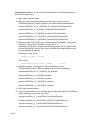
Programming Tab: (image shown for F2808 device)
18 of 37
Algorithm File: Use the same algorithm file that you specified on the Erase Tab.
Flash Data File: This is the .out file that you want to program into the flash.
Timeout: Leave as 0. This option has been superseded by Programming User
Options 4.
User Options 1 through 3: Unused.
User Options 4: : Program acknowledge retry specifier. After sending the DSP
a packet of data to program into the flash, the PC runs a loop that checks for a
program acknowledge from the DSP. This option controls the maximum number
of times the PC will loop. It can generally be left at the default value of 0.
Verify Tab:
Algorithm File: Use the same algorithm file that you specified on the Erase Tab.
Timeout: Leave as 0.
User Options 1 and 2: Unused.
Note: In the JTAG version of SDFlash, these options specify the wait-states for
the OTP and Flash memory to be set before the verify operation starts. The
serial version of SDFlash does not use these options however, and instead the
wait-states remain set to their reset defaults (which are the maximum values).
User Options 3 and 4: Unused
Note that the Verify operation does not perform the word-by-word verify operation
from the Flash API algorithm library. Rather, it performs a simple 16-bit checksum
on the programmed data. Verify is done COFF section by COFF section after all
sections have been programmed. A more complex verify is left to the user to
implement, if desired.
19 of 37
Step 7.
Save the SDFlash project file: Use File->Save Project. Alternately, you can
change the project name at this point if desired by using File->Save Project As.
Step 8.
Power up the DSP and/or reset it so that the bootloader will start. The
Bootloader will wait to Autobaud lock with the host PC.
Step 9.
Reset SDFlash: Click the large red R button in the SDFlash GUI, or you can use
the menus: Device->Reset.
NOTE: The reset button of SDFlash Serial CANNOT reset the DSP target. If the
target is in a bad state or not in bootloader mode then user must use a hardware
reset to get target back to bootloader mode (per step 12). Once that is done the
reset button is used to inform SDFlash that target is in bootloader mode.
Step 10. Erase/Program/Verify the flash. Click the FLASH button on the SDFlash GUI, or
you can use the menus: Device -> Flash.
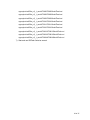
Clicking the FLASH button will bring up the following pop-up window:
Select the desired operations and then click the “Start” button to execute them.
20 of 37
Rebuilding the SDFlash Serial Files
The user will need to rebuild the SDFlash Serial files in the following three situations:
Case 1: You are using a crystal/oscillator for the DSP that does not match the
assumed value. The assumed value is 30 MHz for F281x, and 20 MHz for F280x,
F2801x, and F2804x. If using a different value, the algorithm file
F28yyySerialFlash.out will need to be rebuilt to use a different PLL value.
Case 2: The code security passwords on the device are not all erased (0xFFFF). For
F281x devices, the algorithm file F28yySerialFlash.out will need to be rebuilt to
reflect the passwords in use. For F280x, F2801x, and F2804x devices, the code
security password match flow file F28xxPasswordMF.out will need to be rebuilt to
reflect the passwords in use.
Case 3: You are using a DSP device silicon revision that is not supported by this
version of SDFlash Serial. The SDFlash Serial v3.1 release supports revision C
and later of F2812, F2811, and F2810 devices, and all revisions of F2801, F280160, F2802, F2802-60, F2806, F2808, F2809, F28015, F28016, and F28044
devices. If using an unsupported silicon revision, the algorithm file
F28yyySerialFlash.out will need to be rebuilt with the appropriate flash
programming algorithm APIs.
The Code Composer Studio project file and the source code for the SDFlash Serial
algorithm files are located in:
For F280x-60 devices:
mydrivers\DSP280x_60_v3_1\DSP280x_60_serial\build\F28xxSerialFlash
mydrivers\DSP280x_60_v3_1\DSP280x_60_serial\src
For F280x devices:
mydrivers\DSP280x_v3_1\DSP280x_serial\build\F28xxSerialFlash
mydrivers\DSP280x_v3_1\DSP280x_serial\src
For F281x devices:
mydrivers\DSP281x_v3_1\DSP281x_serial\build\F28xxSerialFlash
mydrivers\DSP281x_v3_1\DSP281x_serial\src
For F2801x devices:
mydrivers\DSP2801x_v3_1\DSP2801x_serial\build\F28xxSerialFlash
mydrivers\DSP2801x_v3_1\DSP2801x_serial\src
For F2804x devices:
mydrivers\DSP2804x_v3_1\DSP2804x_serial\build\F28xxSerialFlash
mydrivers\DSP2804x_v3_1\DSP2804x_serial\src
General instructions for rebuilding the files for the above 3 cases will now be provided.
21 of 37
Instructions for Case 1: You are using a crystal/oscillator for the DSP that does not
match the assumed value.
1) Start Code Composer Studio.
2) Open the CCS project that corresponds to the device you are using, e.g.
F2808SerialFlash.pjt for F2808, located in one of the following sub-directories:
mydrivers\DSP280x_60_v3_1\DSP280x_60_serial\build\F28xxSerialFlash
mydrivers\DSP280x_v3_1\DSP280x_serial\build\F28xxSerialFlash
mydrivers\DSP281x_v3_1\DSP281x_serial\build\F28xxSerialFlash
mydrivers\DSP2801x_v3_1\DSP2801x_serial\build\F28xxSerialFlash
mydrivers\DSP2804x_v3_1\DSP2804x_serial\build\F28xxSerialFlash
3) Edit the constant ‘CPU_RATE’ in the corresponding file Flash280x_Config_API.h,
Flash281x_Config_API.h, Flash2801x_Config_API.h, or
Flash2804x_Config_API.h, and also edit the setting for the PLLCR register in the
function InitSysCtrl() in the file f28xx_main.c to reflect the crystal/oscillator in use.
The relevant lines of code are:
Flash28yyx_Config_API.h:
#define CPU_RATE
10.000L
f28xx_main.c:
SysCtrlRegs.PLLCR.bit.DIV = 0x000A;
// PLLx5
4) Rebuild the project. The output file, F28yyySerialFlash.out (e.g.,
F2808SerialFlash.out for F2808) will appear in the relevant \bin directory:
mydrivers\DSP280x_60_v3_1\DSP280x_60_serial\bin
mydrivers\DSP280x_v3_1\DSP280x_serial\bin
mydrivers\DSP281x_v3_1\DSP281x_serial\bin
mydrivers\DSP2801x_v3_1\DSP2801x_serial\bin
mydrivers\DSP2804x_v3_1\DSP2804x_serial\bin
5) Quit Code Composer Studio.
6) Copy F28yyySerialFlash.out to overwrite the file of the same name in the SDFlash
project directory you are using, e.g. one of:
myprojects\sdf28xx_v3_1_serial\F2801\F2801SerialFlash.out
myprojects\sdf28xx_v3_1_serial\F2801_60\F2801_60SerialFlash.out
myprojects\sdf28xx_v3_1_serial\F2802\F2802SerialFlash.out
myprojects\sdf28xx_v3_1_serial\F2802_60\F2802_60SerialFlash.out
22 of 37
myprojects\sdf28xx_v3_1_serial\F2806\F2806SerialFlash.out
myprojects\sdf28xx_v3_1_serial\F2808\F2808SerialFlash.out
myprojects\sdf28xx_v3_1_serial\F2809\F2809SerialFlash.out
myprojects\sdf28xx_v3_1_serial\F2810\F2810SerialFlash.out
myprojects\sdf28xx_v3_1_serial\F2811\F2811SerialFlash.out
myprojects\sdf28xx_v3_1_serial\F2812\F2812SerialFlash.out
myprojects\sdf28xx_v3_1_serial\F28015\F28015SerialFlash.out
myprojects\sdf28xx_v3_1_serial\F28016\F28016SerialFlash.out
myprojects\sdf28xx_v3_1_serial\F28044\F28044SerialFlash.out
7) Start and use SDFlash Serial as normal.
23 of 37
Instructions for Case 2: The code security passwords on the device are not all
erased (0xFFFF). The instructions differ here for F281x and F280x devices.
For F281x devices:
1) Start Code Composer Studio.
2) Open the CCS project that corresponds to the device you are using, e.g.
F2812SerialFlash.pjt for F2812, located in the following sub-directory:
mydrivers\DSP281x_v3_1\DSP281x_serial\build\F28xxSerialFlash
3) Edit the file Flash2812_API.c so that the defined code security passwords reflect
the passwords in use. All passwords are currently set to the value 0xFFFF. The
relevant lines of code begin at roughly line 63 of the file:
// For
const
const
const
const
const
const
const
const
erased flash the password locations will all
Uint16
PRG_key0 = 0xFFFF;
// PSWD bits
Uint16
PRG_key1 = 0xFFFF;
// PSWD bits
Uint16
PRG_key2 = 0xFFFF;
// PSWD bits
Uint16
PRG_key3 = 0xFFFF;
// PSWD bits
Uint16
PRG_key4 = 0xFFFF;
// PSWD bits
Uint16
PRG_key5 = 0xFFFF;
// PSWD bits
Uint16
PRG_key6 = 0xFFFF;
// PSWD bits
Uint16
PRG_key7 = 0xFFFF;
// PSWD bits
be 0xFFFF
15-0
31-16
47-32
63-48
79-64
95-80
111-96
127-112
4) Rebuild the project. The output file, F28yyySerialFlash.out (e.g.,
F2812SerialFlash.out for F2812) will appear in the \bin directory:
mydrivers\DSP281x_v3_1\DSP281x_serial\bin
5) Quit Code Composer Studio.
6) Copy F28yySerialFlash.out to overwrite the file of the same name in the SDFlash
project directory you are using, e.g. one of:
myprojects\sdf28xx_v3_1_serial\F2810\F2810SerialFlash.out
myprojects\sdf28xx_v3_1_serial\F2811\F2811SerialFlash.out
myprojects\sdf28xx_v3_1_serial\F2812\F2812SerialFlash.out
7) Start and use SDFlash Serial as normal.
24 of 37
For F280x, F2801x, and F2804x devices:
1) Start Code Composer Studio.
2) Open the CCS project F28xxPasswordMF.pjt, located in the following
corresponding directory:
mydrivers\DSP280x_60_v3_1\DSP280x_60_serial\build\F28xxPasswordMF
mydrivers\DSP280x_v3_1\DSP280x_serial\build\F28xxPasswordMF
mydrivers\DSP280x_v3_1\DSP2801x_serial\build\F28xxPasswordMF
mydrivers\DSP280x_v3_1\DSP2804x_serial\build\F28xxPasswordMF
3) Edit the file passwords.inc so that the defined code security passwords reflect the
passwords in use. All passwords currently are set to the value 0xFFFF. The
relevant lines of code are:
.int
.int
.int
.int
.int
.int
.int
.int
0xFFFF
0xFFFF
0xFFFF
0xFFFF
0xFFFF
0xFFFF
0xFFFF
0xFFFF
;PWL0 (LSW of 128-bit password)
;PWL1
;PWL2
;PWL3
;PWL4
;PWL5
;PWL6
;PWL7 (MSW of 128-bit password)
4) Rebuild the project. The output file, F28xxPasswordMF.out will appear in the
corresponding \bin directory:
mydrivers\DSP280x_60_v3_1\DSP280x_60_serial\bin
mydrivers\DSP280x_v3_1\DSP280x_serial\bin
mydrivers\DSP2801x_v3_1\DSP2801x_serial\bin
mydrivers\DSP2804x_v3_1\DSP2804x_serial\bin
5) Quit Code Composer Studio.
6) Copy F28xxPasswordMF.out to overwrite the file of the same name in the
SDFlash project directory you are using, e.g. one of:
myprojects\sdf28xx_v3_1_serial\F2801\F28xxPasswordMF.out
myprojects\sdf28xx_v3_1_serial\F2801_60\F28xxPasswordMF.out
myprojects\sdf28xx_v3_1_serial\F2802\F28xxPasswordMF.out
myprojects\sdf28xx_v3_1_serial\F2802_60\F28xxPasswordMF.out
myprojects\sdf28xx_v3_1_serial\F2806\F28xxPasswordMF.out
myprojects\sdf28xx_v3_1_serial\F2808\F28xxPasswordMF.out
25 of 37
myprojects\sdf28xx_v3_1_serial\F2809\F28xxPasswordMF.out
myprojects\sdf28xx_v3_1_serial\F28015\F28xxPasswordMF.out
myprojects\sdf28xx_v3_1_serial\F28016\F28xxPasswordMF.out
myprojects\sdf28xx_v3_1_serial\F28044\F28xxPasswordMF.out
7) Start and use SDFlash Serial as normal.
26 of 37
Instructions for Case 3: You are using a DSP device or silicon revision that is not
supported by this version of SDFlash Serial. For example, you may be using a new
DSP. To adopt SDFlash Serial for the unsupported device, you will need to obtain
from Texas Instruments the Flash Programming API algorithms for that device. In
addition, these API algorithms must have the same function naming convention used
by the API algorithms originally used to build this version of SDFlash Serial. Assuming
this the case, then:
1) Start Code Composer Studio.
2) If using an unsupported silicon revision: Open the CCS project that corresponds to
the device you are using, e.g. F2808SerialFlash.pjt for F2808, located in one of
the following four sub-directories:
mydrivers\DSP280x_60_v3_1\DSP280x_60_serial\build\F28xxSerialFlash
mydrivers\DSP280x_v3_1\DSP280x_serial\build\F28xxSerialFlash
mydrivers\DSP281x_v3_1\DSP281x_serial\build\F28xxSerialFlash
mydrivers\DSP2801x_v3_1\DSP2801x_serial\build\F28xxSerialFlash
mydrivers\DSP2804x_v3_1\DSP2804x_serial\build\F28xxSerialFlash
27 of 37
3) In Code Composer Studio, click on the menu Project->Build_Options. Select the
Linker tab on the pop-up window, and choose the Libraries Category. Change the
Search_Path and the Incl._Libraries option boxes to reflect the flash API algorithm
library in use:
4) You may also need to modify needed include files or other files used by the flash
API algorithms, e.g., Flash28yyy_API_Config.h. See the documentation provided
with the flash API algorithms for details on this step.
5) Rebuild the project. The output file, F28yyySerialFlash.out (e.g.,
F2808SerialFlash.out for F2808) will appear in the relevant \bin directory:
mydrivers\DSP280x_60_v3_1\DSP280x_60_serial\bin
mydrivers\DSP280x_v3_1\DSP280x_serial\bin
mydrivers\DSP281x_v3_1\DSP281x_serial\bin
mydrivers\DSP2801x_v3_1\DSP2801x_serial\bin
mydrivers\DSP2804x_v3_1\DSP2804x_serial\bin
28 of 37
6) Quit Code Composer Studio.
7) Copy F28yyySerialFlash.out to overwrite the file of the same name in the SDFlash
project directory you are using, e.g. one of:
myprojects\sdf28xx_v3_1_serial\F2801\F2801SerialFlash.out
myprojects\sdf28xx_v3_1_serial\F2801_60\F2801_60SerialFlash.out
myprojects\sdf28xx_v3_1_serial\F2802\F2802SerialFlash.out
myprojects\sdf28xx_v3_1_serial\F2802_60\F2802_60SerialFlash.out
myprojects\sdf28xx_v3_1_serial\F2806\F2806SerialFlash.out
myprojects\sdf28xx_v3_1_serial\F2808\F2808SerialFlash.out
myprojects\sdf28xx_v3_1_serial\F2809\F2809SerialFlash.out
myprojects\sdf28xx_v3_1_serial\F2810\F2810SerialFlash.out
myprojects\sdf28xx_v3_1_serial\F2811\F2811SerialFlash.out
myprojects\sdf28xx_v3_1_serial\F2812\F2812SerialFlash.out
myprojects\sdf28xx_v3_1_serial\F28015\F28015SerialFlash.out
myprojects\sdf28xx_v3_1_serial\F28016\F28016SerialFlash.out
myprojects\sdf28xx_v3_1_serial\F28044\F28044SerialFlash.out
8) Start and use SDFlash Serial as normal.
29 of 37
SDFlash Serial Source File Information
The following is a list of source files used in to make the SDFlash driver file
(F28yxRS232Flash.dll) and the SDFlash Serial flash algorithm file
(F28yyySerialFlash.out), along with a brief description of the files.
-------------------------------------------------------------------Directories: \mydrivers\DSP280x_60_v3_1\DSP280x_60_serial\src
\mydrivers\DSP280x_v3_1\DSP280x_serial\src
\mydrivers\DSP281x_v3_1\DSP281x_serial\src
\mydrivers\DSP2801x_v3_1\DSP2801x_serial\src
\mydrivers\DSP2804x_v3_1\DSP2804x_serial\src
contain Win32 and F28xx shared source files:
drv2808sci.c, drv2808sci.h, drv2812sci.c, drv2812sci.h, drv2801xsci.c,
drv2801xsci.h, drv2804xsci.c, drv2804xsci.h: Low level F28xx serial port driver.
f28xxpkt.c, f28xxpkt.h: Mid level packet code. Supports both Win32 and F28xx build.
lowlev.c, file.h: Optional cio level interface. Ported from TI rts28xx_ml library to support
standard open, close, read, write file functions.
Flash2808_API.c, Flash2812_API.c, Flash2801x_API.c, and Flash2804x_API.c: Thin
wrapper between f28xx_main.c and TI FLASH API. Formats SDFlash arguments into
those required by the TI FLASH API. Ported from TI FLASH API example.
f28xx_main.c, flash.h: Highest level interface for F28xx SDFlash/Serial interface.
-------------------------------------------------------------------Directories: \mydrivers\DSP280x_60_v3_1\DSP280x_60_serial\src_host
\mydrivers\DSP280x_v3_1\DSP280x_serial\src_host
\mydrivers\DSP281x_v3_1\DSP281x_serial\src_host
\mydrivers\DSP2801x_v3_1\DSP2801x_serial\src_host
\mydrivers\DSP2804x_v3_1\DSP2804x_serial\src_host
contain Win32 source files to build the interface between the serial port and SDFlash:
f28xxsio.c, f28xxsio.h: Low level Win32 serial port interface. Uses standard Win32
communications interface.
cofflib.c, coffdefs.h, coff.h, cofflib.h: Spectrum Digital version of TI COFF reader.
f28xxprg.c, f28xxprg.h: The Spectrum Digital PRG interface files. Provides a generic
interface for SDFlash to call. The interface is device independent and could be used to
create any SDFlash based driver.
30 of 37
Troubleshooting Tips
If CONNECTING to the DSP via the serial link fails:
–
Reset the DSP with a hardware reset (i.e., power-cycle the DSP if needed) to be
sure that the bootloader was properly invoked.
–
Check that the DSP is configured for SCI-A bootloader mode.
–
Check that the serial port cable from the host (PC) is connected to SCI-A (as
opposed to SCI-B).
–
Check that the correct host (PC) communications port has been selected in the
SDFlash project settings. In SDFlash, select Project->Settings, and then adjust
Emulator Address/ID on the Target tab.
–
Check that each file specified in the various SDFlash project settings is correct,
especially the paths. Do this carefully, as the eyes can play tricks on you!
Specifying a bad path can result in SDFlash simply reporting a failure to connect.
–
Try lowering the serial baud rate on in the SDFlash project settings. In SDFlash,
select Project->Settings, and then adjust User_Options_3 on the Erase tab.
Baud rate options are described earlier in this document.
–
Make sure the SDFlash Serial algorithms have been re-built to reflect the code
security passwords that you are using. This was discussed earlier in this
document. If you have already rebuilt the algorithms, or are not using the code
security passwords (i.e., all passwords are 0xFFFF), confirm this using Code
Composer Studio and an emulator to unlock the security and view the flash
contents. If you cannot view the flash contents, then there is some sort of code
security problem (e.g., the actual passwords are different than what is thought).
–
Make sure the SDFlash Serial algorithms have been re-built to reflect the DSP
input clock you are using, and an appropriate PLL value. This was discussed
earlier in this document.
–
If using the serial port on the docking station for a laptop PC, try undocking the
laptop and connecting directly to the serial port on the laptop.
–
If you don’t get a failure to connect message, but rather just think SDFlash Serial
has hung (since connecting seems to be taking a long time), make sure you are
waiting long enough before drawing that conclusion. There is a table on page 15
of this document that provides an estimate on the connecting time.
If ERASE fails:
–
Increase the value of Erase User Options #4 in the SDFlash project settings.
If PROGRAM fails:
−
Increase the value of Program User Options #4 in the SDFlash project settings.
31 of 37
References
•
F280x Flash API: Download SPRC193 from the TI website:
http://focus.ti.com/docs/toolsw/folders/print/sprc193.html
•
F281x Flash API: Download SPRC125 from the TI website:
http://focus.ti.com/docs/toolsw/folders/print/sprc125.html
•
F2801x Flash API: Download SPRC327 from the TI website:
http://focus.ti.com/docs/toolsw/folders/print/sprc327.html
•
F2804x Flash API: Download SPRC325 from the TI website:
http://focus.ti.com/docs/toolsw/folders/print/sprc325.html
•
F280x, F2801x, and F2804x Boot ROM and Bootloader info: Download SPRU722
from the TI website:
http://focus.ti.com/docs/prod/folders/print/tms320f2808.html#technicaldocuments
•
F281x Boot ROM and Bootloader info: Download SPRU095 from the TI website:
http://focus.ti.com/docs/prod/folders/print/tms320f2812.html#technicaldocuments
32 of 37
Appendix A: Customizing SDFlash Serial for User Applications
SDFlash Serial is designed as a stand alone utility for programming the flash on
TMS320F28xx. It is assumed that the F28xx device undergoes a reset immediately
before SDFlash Serial is invoked (which starts the ROM bootloader in the F28xx), and
also that the F28xx device is manually reset upon completion of the flash programming
(to begin execution of the code just programmed into the flash). In some applications, it
is desired to use SDFlash Serial to re-program the flash (in the field, for example) without
undergoing one or both of these resets. This Appendix contains information on how to
customize SDFlash to do the following:
•
Invoke SDFlash Serial at Any Time Other Than After a Device Reset
•
Generate a Device Reset After SDFlash Serial Completes
DISCLAIMER: The methods described in this section have undergone only limited
testing, and do alter the original SDFlash Serial source code. They are provided with no
claims made on their proper operation in the user’s application, nor on their suitability for
a particular application. Further, they are included in this documentation only as
suggestions if such features are needed by the user, and are provided without support.
All responsibilities concerning their use lies with the user.
Invoke SDFlash Serial at any Time Other Than After a Device Reset
In the F28xxPasswordMF.pjt project, the file main.asm includes a TRAP #0 instruction at
the end of the password match flow. Normally, if SDFlash Serial is run immediately after
a device reset, the PIE (Peripheral Interrupt Expansion module) is disabled. Therefore,
the TRAP #0 instruction will return a vector value of 0, which traps to the reset vector at
0x3FFFC0 and returns program control to the Boot ROM.
If the PIE is enabled, the TRAP #0 instruction is not allowed and will give indeterminate
results. Therefore, if you invoke SDFlash Serial at any time other than after a device
reset, make sure the PIE is disabled before branching to the start of the bootloader. This
can be done in the user code. Alternately, if the device had been booted from SCI-A
previously and the appropriate boot mode GPIO pins are still externally set to boot from
SCI-A, one could simply force a watchdog reset (e.g., by writing a bad value for the
WDCHK bits in the WDCR register). This will disable the PIE and also invoke the
bootloader.
Generate a Device Reset After SDFlash Serial Completes
Upon completion of flash programming, the F28xx device is left in an endless loop by
SDFlash Serial. Typically, a hardware device reset (e.g., XRSn\ pin) is used to begin
code execution. To have SDFlash Serial automatically generate a reset upon
completion, the user must modify and rebuild the Code Composer Studio
F28yxSerialFlash.pjt project located in the folder
\mydrivers\DSP28yx_v3_1\DSP28yx_serial\build\F28xxSerialFlash. Specifically, the
source file f28xx_main.c must be modified.
33 of 37
Two possible modifications will be described, both of which will generate a device reset.
The first method can introduce a delay between the completion of SDFlash Serial verify
step and the device reset, but it will work for almost any program the user might program
into the device. The second method will reset immediately after SDFlash Serial
completes, but must be customized for every different program that SDFlash Serial
programs into the device.
Both methods assume that SDFlash Serial will be used to Erase, Program, and Verify the
device all at once before resetting the device. Although these solutions are tailored for a
Reset after the Verify stage, they can be slightly modified to occur after the Program or
Erase stage if desired.
Brief Description of f28xx_main.c:
Before going into the details of the two methods, some understanding of the
f28xx_main.c file is required. The main() function in f28xx_main.c includes an infinite forloop in which there is an event loop and then an IDLE instruction. The event loop triggers
on every SCI interrupt event, checks for incoming packet data, and processes that data.
The program will then sit at the IDLE instruction until another packet triggers the event
loop. Once SDFlash Serial finishes, it sits at the IDLE instruction forever.
Modification Method 1:
Instead of sitting at the IDLE instruction forever after the Erase-Program-Verify sequence
has completed, f28xx_main.c can be modified to reset the device after the Verify step
completes. To do this, a count variable can be introduced which is reset to 0 inside of the
event loop. During the Verify stage (last stage in the process), instead of sitting at the
IDLE instruction and waiting for each SCI event, the program will continuously loop in the
infinite for loop and increment the count variable (outside the event loop). As soon as a
new SCI event occurs, indicating there is still incoming packet data, the count variable is
reset to zero. When the Verify step has completed, no new SCI events will occur.
Therefore, the count variable will continue to increase until it reaches some user defined
timeout value. Once the timeout occurs, the program can re-configure GPIO pins as
necessary to configure the bootmode, disable the PIE, and then either branch to the boot
ROM or force a watchdog reset by writing an incorrect value to the WDCHK bits in the
WDCR register.
Code snippets of the above explanation is shown below. The code below includes only
the alterations made to f28xx_main.c and not the entire file. Notice that the count
variable timeout is set at 0x00FFFFFF by default to ensure a suitable timeout period for
almost any program that SDFlash Serial may be programming into the flash (since the
amount of time to program depends on the data being programmed). This timeout value
can be customized by the user to a smaller value if desired.
34 of 37
// CODE CHANGES MADE TO F28XX_MAIN.C FOR METHOD 1
// As a global variable:
Uint32 count;
// In the main() function before the infinite for loop:
PRG_command = 0; //Initilize PRG_command to a null value
count =0; // Initialize count to zero
// In the for loop in main:
//SCI event loop – stripped out everything except what is
//
changed/added for simplicity
while(( gPostedEvents & SCI_EVT_DATA ) == SCI_EVT_DATA )
{
……
count = 0;
//Initialize count to 0 every time an SCI event occurs
……
}
//AFTER SCI event loop, replace the current LED and IDLE
//instructions with:
if (PRG_command == CMD_FLASH_VERIFY) { // Only in Verify Stage
if (count==0x00FFFFFF) {
// if no event has occurred for timeout period
PieCtrlRegs.PIECTRL.bit.ENPIE = 0; // Disable the PIE
asm(" LB
0x003FFB50"); //jump to boot loader in ROM
// above instruction can be replaced by watchdog reset code
} // end count timeout
count++; // if no SCI interrupt, increment count and loop
} //end if verify stage
else {// Idle time btwn pkts in “Program” and “Erase” stages
STATUS_LED_OFF;
asm(" IDLE");
STATUS_LED_ON;
}
After the modifications to f28xx_main.c are complete, the F28xxSerialFlash.pjt project
must be rebuilt using Code Composer Studio. The resulting .out file will appear in the
\bin folder on the same directory level as the \build and \src directories. Copy the .out file
to overwrite the file of the same name in the corresponding device subfolder in the
\myprojects\sdf28xx_v3_1_serial\ directory.
Method 1 is useful in situations where SDFlash Serial might program a variety of different
programs into the device. Therefore, at the end of the Verify stage, for some programs,
there will be some delay while the count variable is timing out before the device is reset.
Once Method 1 is used though, the f28xx_main.c file does not need to be touched again,
even if programming a different file to the device using SDFlash Serial.
35 of 37
Modification Method 2:
Method 2 is a two-stage process which introduces no delay and resets the device
immediately after the Verify step completes, but it requires the f28xx_main.c file to be
customized for each program that is programmed using SDFlash Serial. Therefore,
Method 2 is only useful if the same program is being programmed to multiple devices or
to the same device over and over again. Method 1 is generally preferable unless there is
a requirement for no delay between the completion of the Verify stage and the device
reset.
Stage 1:
First, a verify_count variable is introduced and initialized to 0 at the beginning of the
function main(). The verify_count variable is then incremented within the
FlashExecuteCommand() routine during the Verify step only. In other words, the
verify_count variable is incremented once per receive packet during the Verify step. The
code snippet below shows the declaration and handling of verify_count:
// CODE CHANGES MADE TO F28XX_MAIN.C IN STAGE 1 OF METHOD 2
// As a global variable:
Uint16 verify_count;
// In the main() function before the infinite for loop:
verify_count =0;
// Initialize verify_count to zero
// In the FlashExecuteCommand() function Verify case
case CMD_FLASH_VERIFY:
PRG_status = FLASH28_Verify();
verify_count++;
//Increment verify_count for each packet
EINT;
After the modifications to f28xx_main.c are complete, the F28xxSerialFlash project must
be rebuilt with the new file, and SDFlash Serial must then be run to determine the final
value of verify_count, as follows:
1. Use Code Composer Studio to open the appropriate device project in the
/build/ F28xxSerialFlash/ folder.
2. Re-build the project using the new f28xxmain.c file.
3. Find the appropriate .out file in the /bin folder (same directory level as the
/build and /src directories).
4. Copy the .out file to overwrite the file of the same name in the device specific
sub-folder in the sdflash\myprojects\sdf28xx_v3_1_serial\ directory.
5. In Code Composer Studio, under the File Menu, click “Load Symbols…”
36 of 37
6. Select the .out file you copied previously and click ok.
7. Reset the device in the debugger and hit Run.
8. Run SDFlash Serial to program the flash with the specific code of interest.
9. Once SDFlash Serial finishes, add verify_count to a watch or memory
window and record its value.
Stage 2:
The file f28xxmain.c must be modified again. In main(), before the LED and IDLE
instructions, and after the event loop, add code which performs the desired configuration
and reset actions only if verify_count equals the number found in Stage 1. Basically, the
f28xx_main.c program will run until the last verify packet has been received and
processed. At that point, the program can re-configure GPIO pins as necessary to
configure the bootmode, disable the PIE, and then either branch to the boot ROM or force
a watchdog reset by writing an incorrect value to the WDCHK bits in the WDCR register.
The code required for this stage is shown below:
// CODE CHANGES MADE TO F28XX_MAIN.C IN STAGE 2 OF METHOD 2
// After the event loop and before the LED_STATUS and
if(verify_count==XNUMBER){
//
//
PieCtrlRegs.PIECTRL.bit.ENPIE = 0; //
asm("
LB
0x003FFB50");
//
}
where XNUMBER is replaced by
the number recorded in Stage 1
Disable the PIE
Jump to bootloader in ROM
After the modifications to f28xx_main.c are complete, the F28xxSerialFlash project must
be rebuilt again with the new file:
1. Use Code Composer Studio to open the appropriate device project in the
/build/F28xxSerialFlash/ folder.
2. Re-build the project using the new f28xxmain.c file.
3. Find the appropriate .out file in the /bin folder (same directory level as the /build
and /src directories).
4. Copy the .out file to overwrite the file of the same name in the device specific
sub-folder in the sdflash\myprojects\sdf28xx_v3_1_serial\ directory.
5. Run SDFlash Serial as normal.
As long as the same file is being programmed to the device with SDFlash Serial, no
modifications need to be made to f28xx_main.c. If a different file is being programmed,
the two-stage procedure must be performed again.
37 of 37