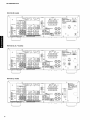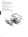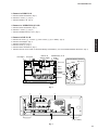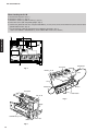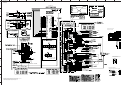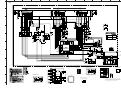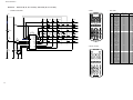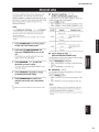
1
DIGITAL HOME THEATER SYSTEM YHT-290/195 AV RECEIVER RX-V363/HTR-6130 SERVICE MANUAL RX-V363/HTR-6130 YHT-290 consists of HTR-6130 and NS-P270D. (C model) YHT-195 consists of HTR-6130 and NS-P270D. (R, K, A, L models) NS-P270D consists of NX-E270, NX-C270 and SW-P270. This service manual is for RX-V363/HTR-6130. For NX-E270, NX-C270 and SW-P270 service manual, please refer to the following service manual: NX-P270/NX-P276: 101000 IMPORTANT NOTICE This manual has been provided for the use of authorized YAMAHA Retailers and their service personnel. It has been assumed that basic service procedures inherent to the industry, and more specifically YAMAHA Products, are already known and understood by the users, and have therefore not been restated. WARNING: Failure to follow appropriate service and safety procedures when servicing this product may result in personal injury, destruction of expensive components, and failure of the product to perform as specified. For these reasons, we advise all YAMAHA product owners that any service required should be performed by an authorized YAMAHA Retailer or the appointed service representative. IMPORTANT: The presentation or sale of this manual to any individual or firm does not constitute authorization, certification or recognition of any applicable technical capabilities, or establish a principle-agent relationship of any form. The data provided is believed to be accurate and applicable to the unit(s) indicated on the cover. The research, engineering, and service departments of YAMAHA are continually striving to improve YAMAHA products. Modifications are, therefore, inevitable and specifications are subject to change without notice or obligation to retrofit. Should any discrepancy appear to exist, please contact the distributor's Service Division. WARNING: Static discharges can destroy expensive components. Discharge any static electricity your body may have accumulated by grounding yourself to the ground buss in the unit (heavy gauge black wires connect to this buss). IMPORTANT: Turn the unit OFF during disassembly and part replacement. Recheck all work before you apply power to the unit. 本资料由OKXIA视听皮带资源库www.okxia.cn提供 ■ CONTENTS TO SERVICE PERSONNEL .......................................... 2 FRONT PANELS ........................................................ 3–4 REAR PANELS .......................................................... 4–9 REMOTE CONTROL PANELS ...................................... 9 SPECIFICATIONS .................................................. 10–12 INTERNAL VIEW ......................................................... 13 DISASSEMBLY PROCEDURES ........................... 14–16 UPDATING FIRMWARE ........................................ 17–19 SELF DIAGNOSTIC FUNCTION ........................... 20–37 101084 DISPLAY DATA ..................................................... 38–39 IC DATA ................................................................. 40–55 BLOCK DIAGRAMS .............................................. 56–57 PRINTED CIRCUIT BOARDS ................................ 58–71 PIN CONNECTION DIAGRAMS .................................. 72 SCHEMATIC DIAGRAMS ...................................... 73–83 REPLACEMENT PARTS LIST .............................. 85–95 REMOTE CONTROL .............................................. 96–98 Advanced setup ........................................................... 99 2008 All rights reserved. This manual is copyrighted by YAMAHA and may not be copied or redistributed either in print or electronically without permission. P.O.Box 1, Hamamatsu, Japan '08.02 RX-V363/HTR-6130 ■ TO SERVICE PERSONNEL 1. Critical Components Information Components having special characteristics are marked s and must be replaced with parts having specifications equal to those originally installed. WALL OUTLET 2. Leakage Current Measurement (For 120V Models Only) When service has been completed, it is imperative to verify that all exposed conductive surfaces are properly insulated from supply circuits. ● Meter impedance should be equivalent to 1500 ohms shunted by 0.15µF. EQUIPMENT UNDER TEST AC LEAKAGE TESTER OR EQUIVALENT INSULATING TABLE ● Leakage current must not exceed 0.5mA. ● Be sure to test for leakage with the AC plug in both polarities. RX-V363/HTR-6130 For U model “CAUTION” “F2251: FOR CONTINUED PROTECTION AGAINST RISK OF FIRE, REPLACE ONLY WITH SAME TYPE 6A, 125V FUSE.” For C model CAUTION F2251: REPLACE WITH SAME TYPE 6A, 125V FUSE. ATTENTION F2251: UTILISER UN FUSIBLE DE RECHANGE DE MÉME TYPE DE 6A, 125V. WARNING: CHEMICAL CONTENT NOTICE! This product contains chemicals known to the State of California to cause cancer, or birth defects or other reproductive harm. DO NOT PLACE SOLDER, ELECTRICAL/ELECTRONIC OR PLASTIC COMPONENTS IN YOUR MOUTH FOR ANY REASON WHAT SO EVER! Avoid prolonged, unprotected contact between solder and your skin! When soldering, do not inhale solder fumes or expose eyes to solder/flux vapor! If you come in contact with solder or components located inside the enclosure of this product, wash your hands before handling food. About lead free solder All of the P.C.B.s installed in this unit and solder joints are soldered using the lead free solder. Among some types of lead free solder currently available, it is recommended to use one of the following types for the repair work. • Sn + Ag + Cu (tin + silver + copper) • Sn + Cu (tin + copper) • Sn + Zn + Bi (tin + zinc + bismuth) Caution: As the melting point temperature of the lead free solder is about 30°C to 40°C (50°F to 70°F) higher than that of the lead solder, be sure to use a soldering iron suitable to each solder. 2 RX-V363/HTR-6130 ■ SPECIFICATIONS ■ Audio Section Minimum RMS Output Power (Power Amp. Section) (1 kHz, 0.9 % THD) FRONT L/R, CENTER, SURROUND L/R U, C models (8 ohms) ........................................ 100 W/ch R, T, K, A, B, G, E, F, L models (6 ohms) ......... 100 W/ch Maximum Power (JEITA) (1 kHz, 10 % THD) FRONT L/R, CENTER, SURROUND L/R U, C models (8 ohms) ........................................ 135 W/ch R, T, K, A, L models (6 ohms) ........................... 135 W/ch RX-V363/HTR-6130 Max. Power Per Channel [B, G, E, F models] (1 kHz, 0.7 % THD, 4 ohms) FRONT L/R, CENTER, SURROUND L/R .... 105 W or more IEC Power [B, G, E, F models] (1 kHz, 0.1 % THD, 6 ohms) MAIN L/R ........................................................ 90 W or more Dynamic Power Per Channel (IHF) (FRONT L/R) U, C models (8/6/4/2 ohms) .................................... 110/130/160/180 W R, T, K, A, B, G, E, F, L models (6/4/2 ohms) .............................................. 105/130/150 W Dynamic Headroom U, C models (8 ohms) ............................................. 0.41 dB Input Sensitivity/Input Impedance (1 kHz, 100 W / 6 ohms) CD, etc. ............................................... 200 mV / 47 k-ohms MULTI CH INPUT FRONT L/R, CENTER, SURROUND L/R, SUBWOOFER ........................................................ 200 mV / 47 k-ohms Maximum Input Signal (1 kHz, 0.5 % THD, Effect on) CD, etc. .......................................................... 2.0 V or more Output Level/Output Impedance REC OUT ........................................... 200 mV / 1.2 k-ohms SUBWOOFER (2 ch STEREO and FRONT SP: Small) ................................................................ 4 V / 1.2 k-ohms Filter Characteristics FRONT, CENTER, SURROUND, SURROUND BACK small (H.P.F.) ....... fc=40/60/80/90/100/110/120/160/200 Hz, 12 dB/oct. SUBWOOFER (L.P.F.) ....... fc=40/60/80/90/100/110/120/160/200 Hz, 24 dB/oct. ■ Video Section Video Signal Type (Gray back) U, C, R, K models ...................................................... NTSC T, A, B, G, E, F, L models ............................................. PAL Composite Video Signal Level .................................................................. 1 Vp-p / 75 ohms Component Signal Level Y ............................................................... 1 Vp-p / 75 ohms Video Maximum Input Level .................................................................. 1.5 Vp-p or more Signal to Noise Ratio (IHF) ....................................................................... 50 dB or more Monitor Out Frequency Response Component video signal .................. 5 Hz to 60 MHz, -3 dB ■ FM Section Tuning Range U, C models ............................................ 87.5 to 107.9 MHz R, L models ............... 87.5 to 108.0 / 87.50 to 108.00 MHz T, K, A, B, G, E, F models ................. 87.50 to 108.00 MHz 50dB Quieting Sensitivity (IHF) (1 kHz, 100 % Mod.) Mono ......................................................... 2.8 µV (20.2 dBf) Headphone Jack Rated Output/Impedance CD, etc. (1 kHz, 200 mV, 8 ohms) ....... 400 mV / 470 ohms Signal to Noise Ratio (IHF) Mono / Stereo ................................................. 73 dB / 70 dB Frequency Response (10 Hz to 100 kHz) CD, etc. to FRONT L/R ..................................... 0 / -3.0 dB (10 Hz to 20 kHz) V-AUX to FRONT L/R ....................................... 0 / -3.0 dB Harmonic Distortion (1 kHz) Mono / Stereo ................................................. 0.5 % / 0.5 % Total Harmonic Distortion (1 kHz, 50 W) CD, etc. (2ch stereo) to FRONT L/R SP OUT U, C models (8 ohms) ................................. 0.06 % or less R, T, K, A, B, G, E, F, L models (6 ohms) ..... 0.06 % or less Signal to Noise Ratio (IHF-A Network) CD, etc. (STEREO) to Input shorted SP OUT 200 mV ........................................................ 98 dB or more 250 mV ...................................................... 100 dB or more Residual Noise (IHF-A Network) FRONT L/R SP OUT .................................... 170 µV or less Channel Separation CD, etc. (Input 5.1 k-ohms shorted, 1 kHz / 10 kHz) ......................................... 60 dB or more / 45 dB or more 10 Tone Control Characteristics BASS Boost/Cut ................................................ ±10 dB (100 Hz) TREBLE Boost/Cut ................................................ ±10 dB (20 kHz) Antenna Input .................................... 75 ohms unbalanced ■ AM Section Tuning Range U, C models .............................................. 530 to 1,710 kHz R, L models ....................... 530 to 1,710 / 531 to 1,611 kHz T, K, A, B, G, E, F models ....................... 531 to 1,611 kHz Antenna Input ................................................. Loop antenna RX-V363/HTR-6130 ■ General • SCENE TEMPLATE Maximum Power Consumption (5 ch drive, 10 % THD) R, L models ............................................................... 530 W Dimensions (W x H x D) ......... 435 x 151 x 317.6 mm (17-1/8" x 5-15/16" x 12-1/2") Weight ................................................. 8.0 kg (17 lbs. 10 oz.) Finish [RX-V363] Gold color ........................................................ T, L models Black color ..................... U, C, R, A, B, G, E, F, L models Silver color ................................... R, A, G, E, F, L models Titanium color ................................... K, B, G, F, L models [HTR-6130] Gold color .............................................................. T model Black color .............................. U, C, R, A, G, F, L models Silver color .......................... U, R, K, A, G, E, F, L models “HDMI”, the “HDMI” logo and “High-Definition Multimedia Interface” are trademarks or registered trademarks of HDMI Licensing LLC. “iPod” is a trademark of Apple Inc., registered in the U.S. and other countries. Bluetooth is a registered trademark of the Bluetooth SIG and is used by Yamaha in accordance with a license agreement. • DIMENSIONS TV Viewing TV Sports Viewing Game Playing Source Movie DVD DVD Music Live DVD DVR DVR DVD-Audio / Music Disc DVD SA-CD / CD DVD CD Music Disc CD CD TUNER/RADIO FM/AM FM/AM (TUNER) DAP iPod DOCK Bluetooth (V-AUX) TV DTV/CBL DTV/CBL GAME V-AUX Mode NIGHT Select (Default) R, T, K, A, B, G, U, C models E, F, L models Sub-mode Mode – Movie Dramatic Pop/Rock Movie Dramatic 2ch Stereo 5ch Stereo 5ch Stereo 2ch Stereo SYSTEM SYSTEM SYSTEM SYSTEM SYSTEM SYSTEM SYSTEM SYSTEM O (SCENE 1) O O O O O (SCENE 2) O O O O (SCENE 1) O O O (SCENE 2) O O O MUSIC ENHANCER Music Enh. 5ch SYSTEM O (SCENE 4) O (SCENE 4) MUSIC ENHANCER Music Enh. 5ch SYSTEM O – STRAIGHT ENTERTAINMENT ENTERTAINMENT SYSTEM SYSTEM SYSTEM O (SCENE 3) O O O (SCENE 3) O O STRAIGHT MOVIE MUSIC MOVIE STEREO STEREO STEREO STEREO – TV Sports Game Sound Field Parameters MUSIC 230 (9-1/16") ENTERTAIN British model European model South European model Russian model Singapore model MOVIE ENHANCER 2ch Stereo 5ch Stereo Pop/Rock Hall Jazz Game TV Sports Movie Spacious Movie Dramatic Music Enh. 2ch Music Enh. 5ch MUSIC ENHANCER LOW, [HIGH] O O O O O O O O O 130 (5-1/8") 21 (13/16") Surround Decoders 395 (15-9/16") 435 (17-1/8") DECODING FORMAT POST DECODING FORMAT Dolby Digital DTS Dolby Pro Logic Dolby Pro Logic II Music Dolby Pro Logic II Movie Dolby Pro Logic II Game PANORAMA ON, [OFF] DIMENSION -3, [STD], +3 CENTER WIDTH 0, 1, 2, [3], 4, 5, 6, 7 O O O 21 (13/16") B .......... G .......... E .......... F .......... L ........... DOCK Listening DVD STEREO * Specifications are subject to change without notice due to product improvements. U.S.A. model Canadian model General model Chinese model Korean model Australian model DVD Viewing DVD Movie Viewing DVD Live Viewing DVR Viewing Music Disc Listening Disc Listening CD Listening CD Music Listening Radio Listening Contents DSP LEVEL MIN, [MID], MAX Accessories ............................................ Remote control x 1 Batteries (R03, AAA, UM-4) x 2 Indoor FM antenna x 1 AM loop antenna x 1 Optimizer microphone x 1 (R, K, A, B, G, E, F, L models) U .......... C .......... R .......... T .......... K .......... A .......... Program SCENE name • SOUND/SURROUND SELECT MENU “DTS” and “DTS Digital Surround” are registered trademarks of DTS, Inc. 21.7 (7/8") Standby Power Consumption (reference data) U, C, T, K, A, B, G, E, F models ................................ 0.8 W “SILENT CINEMA” is a trademark of Yamaha Corporation. 274.9 (10-13/16") 317.6 (12-1/2") Power Consumption U, C models ................................................ 240 W / 320 VA R, T, K, A, B, G, E, F, L models ................................ 240 W Manufactured under license from Dolby Laboratories. “Dolby”, “Pro Logic”, and the double-D symbol are trademarks of Dolby Laboratories. 151 (5-15/16") Power Supply U, C models ............................................... AC 120 V, 60 Hz R, L models .................... AC 110-120/220-240 V, 50/60 Hz T model ..................................................... AC 220 V, 50 Hz K model ..................................................... AC 220 V, 60 Hz A model ..................................................... AC 240 V, 50 Hz B, G, E, F models ...................................... AC 230 V, 50 Hz Unit: mm (inch) 11 12 CATEGORY SPEAKER LEVEL SUB MENU • • • • • || • • • • • • • • • • || • • • • • C SL • • • • • || • • • • • SWFR • • • • • || • • • • • SR • • • • • || • • • • • FR SELECT MENU ROOM :M SUBWOOFER : YES SPEAKERS : 5 spk SET / [CANCEL] CHECK : Test Tone CHECK OK? FL • • • • • || • • • • • SIGNAL INFO 1 2 3 4 5 BITRATE (Bit rate) FLAG FORMAT (Signal format) SAMPLING CHANNEL (U, C models) PARAM. INI BLUETOOTH AUDIO SELECT MEMORY GUARD MULTI CH SET DISPLAY SET D) DECODER MODE C) VOLUME TRIM B) INPUT RENAME A) INPUT ASSIGN G) AUDIO SET F) D. RANGE E) LFE LEVEL D) CENTER GEQ C) SP DISTANCE B) SP LEVEL A) SPEAKER SET E) 3 OPTION MENU A) B) C) D) E) 2 INPUT MENU MANUAL SETUP 1 SOUND MENU L models) • • • • • || • • • • • • • • • • || • • • • • C SL meters : 0.30 to 24.00 m, [2.40 m], 0.10 m step meters : 0.30 to 24.00 m, [3.00 m], 0.10 m step feet : 1.0 to 80.0 ft, [10.0 ft], 0.5 ft step feet : 1.0 to 80.0 ft, [8.0 ft], 0.5 ft step feet : 1.0 to 80.0 ft, [10.0 ft], 0.5 ft step feet (ft) / meters (m) -10 to +10 dB, [0 dB], 1 dB step : OFF :0 : DVD : CD : DTV/CBL : 0 ms : +16 dB : OFF : MAX : MAX : FULL : 0 dB : 0 dB 0 dB 0 dB 0 dB 0 dB 0 dB Capital: A to Z, Small: a to z, Figure: 0 to 9, Space, Marks: # * + , - . / : < > ? CD / TUNER / MD/CD-R / DVD / DTV/CBL / V-AUX (DOCK: U, C models) / DVR / MULTI CH INPUT -6.0 to +6.0 dB, [0.0 dB], 1.0 dB step [AUTO] / LAST [AUTO] / DTS [LAST] / DVR / V-AUX / DTV/CBL / DVD -4 to 0, [0], 1 step [OFF] / ON [AUTO] / LAST [NO] / YES [FULL] / -20 dB 0 to 160 ms, [0 ms], 1 ms step +16 dB / +10 to -30 dB, [+16 dB], 5 dB step OFF / -80 to +16 dB, [OFF], 1 dB step CD / MD/CD-R / [DVD] / DTV/CBL / V-AUX / DVR [CD] / MD/CD-R / DVD / DTV/CBL / V-AUX / DVR CD / MD/CD-R / DVD / [DTV/CBL] / V-AUX / DVR CD / MD/CD-R / DVD / DTV/CBL / V-AUX / DVR Input is possible to 8 characters Input possible Character type: MIN / STD / [MAX] -20 to 0 dB, [0 dB], 1 dB step -6.0 to +6.0 dB, [0 dB], 0.5 dB step meters : 0.30 to 24.00 m, [3.00 m], 0.10 m step : > OFF ON [OFF] / ON : 3.00 m : 3.00 m VALUE [INITIAL] [FRONT] / ZONE B [LARGE] / SMALL NONE / [SML] / LRG NONE / [SML] / LRG SWFR / FRNT / [BOTH] 40 / 60 / [80] / 90 / 100 / 110 / 120 / 160 / 200 Hz [NRM] / REV -10 to +10 dB, [0 dB], 1 dB step [YES] / NO S / [M] / L [YES] / NONE 2 spk / 3 spk / 4 spk / [5 spk] Analog / PCM / Dolby Digital / DTS / Digital / --- / ??? xxx kHz 2/0/--- / 3/2/0.1 / 1+1/0/--- / ---/--xxx kbps DTS / Dolby Digital / PCM / None START PAIRING CD / DVD / DTV/CBL BGV DIMMER MEM. GUARD > AUTO LAST : 3.00 m : 3.00 m : 3.00 m : 3.00 m : 10.0 ft SWFR : 10.0 ft SUR. R FRONT L FRONT R CENTER SUR. L SUR. R SWFR TEST 100 Hz - - || - 300 Hz - - || - 1 kHz - - || - 3 kHz - - || - 10 kHz - - || - SP LFE HP LFE SP D. R. HP D. R. MUTE TYP A. DELAY MAX VOL. INI. VOL. IN (1) [COAXIAL] IN (2) [OPTICAL] IN (3) [OPTICAL] : 10.0 ft : 10.0 ft CENTER : 10.0 ft FRONT R SUR. L : feet : 10.0 ft UNIT FRONT L • • • • • || • • • • • SWFR • • • • • || • • • • • SR • • • • • || • • • • • FR FRONT B : FRONT FRONT : LARGE CENTER : SML SUR. L/R : SML BASS OUT : BOTH CROSSOVER : 80 Hz SWFR PHASE : NRM FL • • • • • || • • • • • (R, K, A, B, G, E, F, Use this feature to automatically adjust speaker and system parameters. AUTO SETUP (U, C, T models) MAIN MENU SET MENU TABLE BASIC SETUP • RX-V363/HTR-6130 RX-V363/HTR-6130 ■ INTERNAL VIEW 1 2 3 4 5 C D A E 7 8 0 9 1 2 3 4 5 6 7 8 9 0 A B C D E F Power Transformer OPERATION (3) P.C.B. OPERATION (5) P.C.B. (R, L models) MAIN (3) P.C.B. Tuner HDMI P.C.B. OPERATION (4) P.C.B. DSP P.C.B. MAIN (4) P.C.B. MAIN (1) P.C.B. OPERATION (2) P.C.B. OPERATION (11) P.C.B. OPERATION (6) P.C.B. OPERATION (10) P.C.B. OPERATION (1) P.C.B. OPERATION (7) P.C.B. RX-V363/HTR-6130 B 6 F 13 RX-V363/HTR-6130 ■ DISASSEMBLY PROCEDURES (Remove parts in the order as numbered.) Disconnect the power cable from the AC outlet. 1. Removal of Top Cover a. Remove 4 screws (1), 4 screws (2) and 1 screw (3). (Fig. 1) b. Slide the top cover rearward to remove it. (Fig. 1) 2. Removal of Front Panel Unit RX-V363/HTR-6130 a. Remove 6 screws (4). (Fig. 1) b. Remove CB192, CB234, CB261 and CB408. (Fig. 1) c. Release hook and then remove the front panel unit. (Fig. 1) 2 3 Top cover 1 Front panel unit 2 CB261 4 CB234 CB408 4 CB192 Hook 4 Fig. 1 14 RX-V363/HTR-6130 3. Removal of HDMI P.C.B. a. Remove CB904 and CB905. (Fig. 2) b. Remove 5 screws (5). (Fig. 3) c. Remove HDMI P.C.B.. (Fig. 2) 4. Removal of OPERATION (4) P.C.B. a. Remove CB193 and CB182. (Fig. 2) b. Remove 7 screws (6). (Fig. 3) c. Remove OPERATION (4) P.C.B.. (Fig. 2) 5. Removal of DSP P.C.B. RX-V363/HTR-6130 a. b. c. d. e. f. Remove 18 screws (7), 3 screws (8) and 2 screws (9) (R, L models). (Fig. 3) Remove cord stopper. (Fig. 2) Remove rear panel. (Fig. 2) Remove screw (0). (Fig. 2) Remove CB512 and CB516. (Fig. 2) Remove the DSP P.C.B. which is connected directly to the MAIN (1) P.C.B. with board-to-board connectors. (Fig. 2) Cord stopper Rear panel HDMI P.C.B. CB904 CB905 OPERATION (4) P.C.B. CB181 CB182 DSP P.C.B. • Board-to-board connectors DSP P.C.B. CB502 CB501 CB512 CB516 0 CB193 CB164 CB101 MAIN (1) P.C.B. Fig. 2 6 5 7 8 9 (R, L models) Fig. 3 15 RX-V363/HTR-6130 When checking the P.C.B. a. b. c. d. e. Remove the Top cover. (Fig. 1) Remove 3 screws (8). (Fig. 3) Remove 5 screws (A) and 4 screws (B). (Fig. 4) Place the P.C.B.s (with rear panel) upright. (Fig. 5) Connect the ground of heat sink, rear panel and MAIN (1) P.C.B. (G103, G104, G105 and ST101) to the chassis with a ground lead or the like. (Fig. 5) • Use the extension cable for connection for the following connectors. (Fig. 6) DSP P.C.B. CB408 – OPERATION (1) P.C.B. CB202: MF117350 (17P, 300mm) B RX-V363/HTR-6130 A A A Rear panel Ground lead Fig. 4 MAIN (1) P.C.B. G104 G103 G105 ST101 Ground lead Chassis Rear panel Ground lead DSP P.C.B. Fig. 5 CB408 OPERATION (1) P.C.B. MF117350 CB202 Fig. 6 16 RX-V363/HTR-6130 ■ UPDATING FIRMWARE After replacing the following parts, be sure to write the latest firmware. • DSP P.C.B. • IC201 (DSP P.C.B.) ● Required Tools • • • • ● Operation Procedures DVD or CD player (with DIGITAL OUTPUT (OPTICAL or COAXIAL) jack) Optical cable (when OPTICAL jack is used) Digital audio pin cable (when COAXIAL jack is used) Firmware CD * To make the firmware CD, download the latest firmware from the specified download source to PC. 1. Connect this unit and DVD/CD player as shown below. (Fig. 1) RX-V363/HTR-6130 Example of connection between digital OPTICAL jacks This unit DVD/CD player Optical cable Example of connection between digital COAXIAL jacks This unit DVD/CD player Digital audio pin cable Fig. 1 17 RX-V363/HTR-6130 RX-V363/HTR-6130 2. While simultaneously pressing the “STANDBY/ON” and “SPEAKERS A/B/OFF” keys of this unit, connect the power cable of this unit to the AC outlet. (Fig. 2) The FIRMWARE UPDATE mode is activated and “SPDIF Upgrade” is displayed. (Fig. 2) "STANDBY/ON" key "SPEAKERS A/B/OFF" key FIRMWARE UPDATE mode SPDIF Upgrade Fig. 2 3. 4. 5. 6. 7. Connect the power cable of DVD/CD player to the AC outlet. Press the “STANDBY/ON” key of the DVD/CD player. Press the “EJECT” key of the DVD/CD player to open the disc tray. Place the firmware CD in the disc tray and close the disc tray. Press the “PLAY” key of the DVD/CD player. Then writing of the firmware is started. (Fig. 3) 8. When writing of the firmware is completed, “Upgrade OK”, “Please...” and “Turn off!!” are displayed repeatedly. (Fig. 3) Writing is started. Writing is completed. Address:XXXXXX Upgrade OK XXXXXX: Address information of the received data Please... Turn off!! Fig. 3 18 RX-V363/HTR-6130 * When the version of the firmware to be written is the same as the one existing in this unit, “Same Version”, “Please...” and “Turn off!!” are displayed repeatedly. (Upgrading is not necessary.) If the display remains unchanged for more than 10 seconds after starting the firmware CD play procedure, perform the firmware CD play procedure again from the beginning. If “FILE CORRUPTED” is displayed after “Address:XXXXXX”, make sure that the firmware CD is not corrupted and perform steps 1 to 8 of “Operation Procedures” again. If “Upgrade Failed” is displayed, perform Steps 1 to 8 of “Operation Procedures” again. RX-V363/HTR-6130 9. Press the “STOP” key of the DVD/CD player. 10. Press the “EJECT” key of the DVD/CD player to open the disc tray. 11. Remove the firmware CD from the disc tray and close the disc tray. 12. Turn off the power of the DVD/CD player and disconnect the power cable from the AC outlet. 13. Turn off the power by pressing the “STANDBY/ON” key of this unit. ● Confirmation of firmware version and checksum To confirm that the firmware is updated successfully, check the firmware version and checksum value by using the selfdiagnostic function menu “14. ROM VER/SUM”. For more information, refer to “SELF DIAGNOSTIC FUNCTION”. * When the displayed firmware version and checksum are different from written firmware version and checksum, follow the steps from 1 to 13 of “Operation Procedures” again. ● Initializing of this unit * After updating the firmware, be sure to initialize this unit. 1. Connect the power cable of this unit to the AC outlet. 2. Press the “STANDBY/ON” key while simultaneously pressing the “STRAIGHT” and “AUDIO SELECT” keys. (Fig. 5) The self-diagnostic function is activated. 3. Select the main menu “13. FACTORY PRESET”. 4. Select the “PRESET RSRV”. PRESET INHIBIT (Initialization inhibited) 13.PRESET INHI PRESET RESERVED (Initialization reserved) 13.PRESET RSRV 5. Turn off the power of this unit and disconnect the power cable from the AC outlet. 19 RX-V363/HTR-6130 ■ SELF DIAGNOSTIC FUNCTION This unit has self diagnosis functions that are intended for inspection, measurement and location of faulty point. There are 14 main menu items, each of which has sub-menu items. Listed in the table below are menu items and sub-menu items. Note that not all menu items listed will apply to the models covered in this service manual. RX-V363/HTR-6130 No. 1 20 Main menu BYPASS 2 AUDIO CHECK 3 SPEAKERS SET 4 6CH-INPUT 5 6 MIC CHECK FL CHECK 7 TEST TONE 8 PROTECTION 9 AD DATA CHECK Sub-menu ANALOG BYPASS DSP BYPASS AUDIO CHECK MUTE ALL MUTE SYSTEM IC MUTE TRUNSISTOR FRNT : SML 0dB CENTER : NONE LFE/B : FRNT TONE : MAX TONE : MIN 6ch INPUT 6-ohm 6ch INPUT 8-ohm LIM : , PLDET : , THM : MIC CHECK VFD CHECK VFD DISP OFF VFD DISP ALL VFD DIMMER CHECK PATTERN TEST ALL TEST FRNT L TEST CENTER TEST FRNT R TEST SURR R TEST SURR L TEST LFE PRD L : xxx PRD H : xxx PRV L : xxx PRV H : xxx THM : xxx PLDET8_L : xxx PLDET8_H : xxx PLDET6_L : xxx PLDET6_H : xxx PRI : xxx PDET : xxx PD : xxx PV : xxx TH : xxx PL : xxx PI : xxx DE : xxx K0 : xxx K1 : xxx RX-V363/HTR-6130 Main menu PROTECTION HISTORY 11 iPod 12 SOFT SW 13 FACTORY PRESET 14 ROM VER/SUM Sub-menu History 1 History 2 History 3 History 4 DOCK : xxx DOCK ignore SW MODE MODEL DESTINATION TUNER DESTINATION VIDEO FORMAT AAC YPAO RDS DOCK (iPod) PRESET INHI PRESET RSRV TOTAL VERSION CRC14 ALL program CRC16 apprication & standby (Main program CRC16) CRC16 SPI F/W update code CRC16 S/PDIF/ F/W update code FLASH ROM Read/Write check SDRAM Read/Write check EEPROM Read/Write check RX-V363/HTR-6130 No. 10 21 RX-V363/HTR-6130 • Starting Self-diagnostic Function Press the “STANDBY/ON” key while simultaneously pressing those two keys of this unit as indicated in the figure below. Keys of this unit RX-V363/HTR-6130 Turn on the power while pressing these keys. • Starting Self-diagnostic Function in the protection cancel mode If the protection function works and causes hindrance to trouble diagnosis, cancel the protection function as described below, and it will be possible to enter the self-diagnostic function mode. (The protection functions other than the excess current detect function will be disabled.) Press the “STANDBY/ON” key while simultaneously pressing those two keys indicated in the figure above. At this time, keep pressing those two keys for 3 seconds or longer. In this mode, the [SLEEP] segment of the FL display of this unit flashes to indicate that the mode is self-diagnostic function mode with the protection functions disabled. CAUTION! Using this product with the protection function disabled may cause damage to this unit. Use special care for this point when using this mode. • Canceling Self-diagnostic Function 1. Before canceling self-diagnostic function, execute setting for FACTORY PRESET of main menu No.13 (Memory initialization inhibited or Memory initialized). * In order to keep the user memory stored, be sure to select PRESET INHIBITED (Memory initialization inhibited). 2. Turn off the power by pressing the “STANDBY/ON” key of this unit. • Display provided when Self-diagnostic Function started On the FL display of this unit, an opening message (including the protection history) appears for a few seconds followed by the self-diagnostic function menu display (1. ANALOG BYPASS). 22 RX-V363/HTR-6130 When there is no history of protection function: When there is no protection history After a few seconds NO PROTECTION 1.ANLOG BYPASS When there is a history of protection function due to excess current PRI PRT:xxx RX-V363/HTR-6130 AD value when the protection function is working Cause: An excessive current flowed through the power amplifier. Supplementary information: As current of the power amplifier is detected, the abnormal channel can be identified by checking the current detect transistor. Turning on the power without correcting the abnormality will cause the protection function to work immediately and the power supply will instantly be shut off. Note) • Applying the power to this unit without correcting the abnormality can be dangerous and cause additional circuit damage. To avoid this, if “PRI” and “PRD” protection function has been activated 3 times continuously, the power will not turn on even when the “STANDBY/ON” key is pressed. In order to turn on the power again, disconnect the power cable of this unit from the AC outlet once and then reconnect it again. • The output transistors in each amplifier channel should be checked for damage before applying power to this unit. • Amplifier current should be monitored by measuring DC voltage across the emitter resistors for each channel. When there is a history of protection function due to abnormal DC output PRD PRT:xxx AD value when the protection function is working Cause: DC output of the power amplifier is abnormal. Supplementary information: The protection function worked due to a DC voltage appearing at the speaker terminal. A cause could be a defect in the amplifier. If the power is turned on with the abnormality unsolved, the protection function works in about 3 seconds to turn off the power. 23 RX-V363/HTR-6130 When there is a history of protection function due to abnormal voltage in the power supply section PRV PRT:xxx AD value when the protection function is working RX-V363/HTR-6130 Cause: The voltage in the power supply section is abnormal. Supplementary information: The protection function worked due to a defect or overload in the power supply. If the power is turned on with the abnormality unsolved, the protection function works in about 1 second to turn off the power. When there is a history of protection function due to excessive heat sink temperature THM PRT:xxx AD value when the protection function is working Cause: The temperature of the heat sink is excessive. Supplementary information: The protection function worked due to the temperature limit being exceeded. Causes could be poor ventilation or a defect related to the thermal sensor. If the power is turned on with the abnormality unsolved, the protection function works in about 1 second to turn off the power. For detection of each protection function, refer to main menu described later. History of protection function When the protection function has worked, its history is stored in memory with a backup. Even if no abnormality is noted while servicing the unit, an abnormality which has occurred previously can be defined as long as the backup data has been stored. The history of the protection function is cleared when self-diagnostic function is cancelled by selecting PRESET RESERVED (Memory initialized) of main menu No. 13 or when the backup data is erased. 24 RX-V363/HTR-6130 • Operation procedure of Main menu and Sub-menu There are 14 menu items, each of having sub-menu items. Main menu selection: Select the menu using “>” (forward) and “<” (reverse) keys of PROGRAM. Sub-menu selection: Select the sub-menu using “SCENE 2” (forward) and “SCENE 1” (Reverse) keys. Keys of this unit Sub-menu selection Reverse RX-V363/HTR-6130 Reverse Forward Forward Main menu selection • Functions in Self-Diagnostic Function mode In addition to the self-diagnostic function menu items, functions as listed below are available. • Power on/off • Master volume • Muting • Speakers A/B/OFF • Input selection • Audio select • Tone control * Functions related to the tuner and the set menu are not available. • Initial settings used to start Self-Diagnostic Function The following initial settings are used when starting self-diagnostic function. When self-diagnostic function is canceled, these settings are restored to those before starting self-diagnostic function. • Master volume: -20 dB • Input: DVD (MULTI CHANNEL INPUT OFF) • Effect level: 0 dB • Main menu: 1. ANALOG BYPASS 25 RX-V363/HTR-6130 • Details of Self-Diagnostic Function menu 1. BYPASS Using the sub-menu, it is possible to select ANALOG BYPASS output or DSP BYPASS output. ANALOG BYPASS The analog input sound signal is output to FRONT L/R with EFFECT OFF. 1.ANLOG BYPASS RX-V363/HTR-6130 INPUT: DVD ANALOG SPEAKER OUT: 1 kHz, SUBWOOFER OUTPUT: 50 Hz Input level Volume Both ch, -20 dBm +6.0 dB FRONT +11.5 dBm SPEAKER OUT CENTER -∞ SURROUND -∞ SUBWOOFER OUTPUT -∞ SURROUND -∞ SUBWOOFER OUTPUT -∞ DSP BYPASS The digital input sound signal is output to FRONT L/R with EFFECT OFF. 1.DSP BYPASS INPUT: DVD ANALOG SPEAKER OUT: 1 kHz, SUBWOOFER OUTPUT: 50 Hz Input level Volume Both ch, -20 dBm +6.0 dB FRONT +11.5 dBm SPEAKER OUT CENTER -∞ 2. AUDIO CHECK The input sound signal is output. * When the inputted sound signal is 2 ch L/R, it is distributed as follows when output. L ch: FRONT L, CENTER, SURROUND L, LFE ( L ch +10 dB) R ch: SURROUND R 2.AUDIO CHECK INPUT: DVD ANALOG SPEAKER OUT: 1 kHz, SUBWOOFER OUTPUT: 50 Hz Input level Volume Both ch, -20 dBm +6.0 dB FRONT +11.5 dBm SPEAKER OUT CENTER +11.5 dBm MUTE ALL 2.MUTE ALL MUTE SYSTEM IC 2.MUTE SYS IC MUTE TRANSISTOR 2.MUTE TR 26 SURROUND +11.5 dBm SUBWOOFER OUTPUT 0 dBm RX-V363/HTR-6130 3. SPEAKER SET The analog switch settings for each sub-menu are as shown in the table below. FRONT CENTER LFE/B TONE TONE : SML 0dB : NONE : FRNT : MAX : MIN SMALL LARGE LARGE LARGE LARGE LARGE NONE SMALL LARGE LARGE LARGE LARGE SMALL LARGE LARGE SWFR SWFR FRONT SWFR SWFR 3.FRNT:SML 0dB FRONT: SML 0dB The FRONT L/R signal, when 90 Hz or lower, is mixed to the channel specified by LFE/BASS. 3.CENTER NONE CENTER: NONE The CENTER signal is distributed to FRONT L/R. 3.LFE/B:FRNT LFE / BASS: FRONT The LFE (SUBWOOFER) signal is distributed to FRONT L/R. 3.TONE:MAX TONE: MAX The signal is output with the tone control [BASS +10 dB, TREBLE +10 dB]. 3.TONE:MIN TONE: MIN The signal is output with the tone control [BASS -10 dB, TREBLE -10 dB]. RX-V363/HTR-6130 LARGE: This mode is used for a speaker with high bass reproduction performance (a large unit). Full bandwidth signals are output. SMALL: This mode is used for a speaker with low bass reproduction performance (a small unit). The signals of 90 Hz or less are mixed into the channel specified by LFE/BASS. NONE: This mode is used for no center speaker. The center content is reduced by 3 dB and distributed to FRONT L/R. SWFR: LFE of 5.1 ch signal or LFE/BASS lower than 90 Hz is output through SUBWOOFER OUT. FRONT: LFE of 5.1 ch signal or LFE/BASS lower than 90 Hz is distributed to FRONT L/R. INPUT: DVD ANALOG SPEAKER OUT: 1 kHz, SUBWOOFER OUTPUT: 50 Hz Sub-menu FRONT CENTER LFE/B TONE TONE : SML 0dB : NONE : FRNT : MAX : MIN Input level Volume Both ch, -20 dBm Both ch, -20 dBm Both ch, -20 dBm Both ch, -20 dBm Both ch, -20 dBm +6.0 dB +6.0 dB +6.0 dB +6.0 dB +6.0 dB FRONT +11.5 dBm +11.5 dBm +11.5 dBm +14.5 dBm +8.5 dBm SPEAKER OUT CENTER -∞ -∞ -∞ -∞ -∞ SURROUND -∞ -∞ -∞ -∞ -∞ SUBWOOFER OUTPUT -3.5 dBm -∞ -∞ -∞ -∞ 27 RX-V363/HTR-6130 4. 6CH INPUT The input source [MULTI CHANNEL INPUT] is selected. It is possible to select the 6-ohm/8-ohm by using the sub-menu. 6 ch INPUT 6-ohm 4.6ch INPUT 6 Ω RX-V363/HTR-6130 INPUT: MULTI CH INPUT SPEAKER OUT: 1 kHz, SUBWOOFER OUTPUT: 50 Hz Sub-menu Input level Volume 6 ch INPUT 6-ohm Both ch, -20 dBm +6.0 dB FRONT +11.5 dBm SPEAKER OUT CENTER +11.5 dBm SURROUND +11.5 dBm SUBWOOFER OUTPUT -3.5 dBm SURROUND +11.5 dBm SUBWOOFER OUTPUT -3.5 dBm 6 ch INPUT 8-ohm 4.6ch INPUT 8 Ω INPUT: MULTI CH INPUT SPEAKER OUT: 1 kHz, SUBWOOFER OUTPUT: 50 Hz Sub-menu Input level Volume 6 ch INPUT 8-ohm Both ch, -20 dBm +6.0 dB FRONT +11.5 dBm SPEAKER OUT CENTER +11.5 dBm LIM/PLDET/THM LIM: Setting value of LIM (Limiter control) * Do not change the setting value because this item is only for the use of development staff. PLDET: Power limiter detection The A/D conversion value during operation is displayed. THM: Thermo protection detection The A/D conversion value during operation is displayed. (Reference voltage: 3.3 V=255) 4.255:255: 82 THM (Thermo protection detection) PLDET (Power limiter detection) LIM (Limiter control) 5. MIC CHECK The signals input through the microphone are output of FRONT L/R via A/D and D/A. 5.MIC CHECK 28 RX-V363/HTR-6130 6. FL CHECK Use this program to check the FL display section. For audio signal processing, use STRAIGHT. Checking FL display section Initial display RX-V363/HTR-6130 All segments OFF All segments ON (dimmer 100%) All segments ON (dimmer 50%) Lighting of segments in lattice 29 RX-V363/HTR-6130 7. TEST TONE RX-V363/HTR-6130 The outputs the noise through the channels specified by the submenu. The noise frequency for LFE (SUBWOOFER) is 35 to 80 Hz. Other than that, the noise frequency is 500 to 2 kHz. 30 7.TEST ALL TEST ALL Noise is output from all channels. 7.TEST FRNT L TEST FRONT L Noise is output from the FRONT L channel. 7.TEST CENTER TEST CENTER Noise is output from the CENTER channel. 7.TEST FRNT R TEST FRONT R Noise is output from the FRONT R channel. 7.TEST SURR R TEST SURROUND R Noise is output from the SURROUND R channel. 7.TEST SURR L TEST SURROUND L Noise is output from the SURROUND L channel. 7.TEST LFE TEST LFE (SUBWOOFER) Noise is output from the LFE (SUBWOOFER) channel. RX-V363/HTR-6130 8. PROTECTION The A/D setting value of each protection is displayed. (Reference voltage: 3.3 V=255) 35 PRD (Amplifier DC protection) Low The minimum preset value of PRD is displayed. 8.PRD H : 81 PRD (Amplifier DC protection) High The maximum preset value of PRD is displayed. 8.PRV L : 83 PRV (Voltage protection) Low The minimum preset value of PRV is displayed. 8.PRV H : 153 PRV (Voltage protection) High The maximum preset value of PRV is displayed. 8.THM THM (Thermo protection) High The maximum preset value of THM is displayed. : 128 8.PLD8 L: 77 PLD (PLDET (Power limiter detection)) 8-ohm Low The value for starting limiter operation of PLD8 is displayed. 8.PLD8 H: 100 PLD (PLDET (Power limiter detection)) 8-ohm High The value for canceling limiter operation of PLD8 is displayed. 8.PLD6 L: 77 PLD (PLDET (Power limiter detection)) 6-ohm Low The value for starting limiter operation of PLD6 is displayed. 8.PLD6 H: 100 PLD (PLDET (Power limiter detection)) 6-ohm High The value for canceling limiter operation of PLD6 is displayed. 8.PRI 100 PRI (Amplifier current protection) High The maximum preset value of PRI is displayed. 8.PDET 209 PDET Low The minimum preset value of PDET is displayed. RX-V363/HTR-6130 8.PRD L : 31 RX-V363/HTR-6130 9. A/D DATA CHECK This menu is used to display the A/D conversion value of the microprocessor which detects panel keys of this unit and protection functions in using the sub-menu. When K0/K1 menu is selected, keys become non-operable due to detection of the values of all keys. However, it is possible to advance to the next sub-menu by turning the VOLUME of this unit. When using this function, note that turning the VOLUME more than 1 click would cause the volume value to change. Signal processing is maintained in the status before execution. * The figures in the diagram are given as reference only. PD/PV PD: RX-V363/HTR-6130 PV: PRD (Power amplifier DC protection detection) The output of power amplifier DC (DC voltage) is detected. Normal value: 35 to 81 (Reference voltage: 3.3 V=255) PRV (Voltage protection detection) Voltage detects: ACL, AC2, 10V, S9, +12, -12, +5V and VP Normal value: 84 to 153 (Reference voltage: 3.3 V=255) * If PRD and PRV are out of the normal value range, the protection function works to turn off the power. PD: 57 PV:128 TH/PL TH: THM (Thermo protection detection) The temperature of the heat sink is detected. Normal value: 0 to 124 (Reference voltage: 3.3 V=255) * If THM is out of the normal value range, the protection function works to turn off the power. PL: PLDET (Power limiter detection) The output voltage of power amplifier is detected. TH: 77 PL:255 U, C models (Reference voltage: 3.3 V=255) PLDET LIM H: 255 / L: 102 (LIM: Limiter control) During normal operation 255 H Value for starting limiter operation 77 L Value for canceling limiter operation 100 H R, T, K, A, B, G, E, F, L models (Reference voltage: 3.3 V=255) PLDET LIM H: 255 / L: 90 (LIM: Limiter control) PI/DE PI: DE: During normal operation 255 H Value for starting limiter operation 100 L Value for canceling limiter operation 131 H PRI (Current protection detection) The current of the power amplifier is detected. Normal value: 0 to 100 (Reference voltage: 3.3 V=255) PDET (Sub-trans power detection) Normal value: 209 to 255 (Reference voltage: 3.3 V=255) * If PRI and PDET are out of the normal value range, the protection function works to turn off the power. PI: 12 DE:255 32 RX-V363/HTR-6130 K0/K1 K0/K1: KEY0/KEY1 (Panel key of this unit) The key will fail to function properly if its A/D conversion value deviates more than ±4 from reference value. In that case, check the constant of partial pressure resistor, solder condition, etc. with referring to the table below. (Reference voltage: 3.3 V=255) K0:255 K1:255 KEY0 SCENE 1 SCENE 2 PROGRAM < PROGRAM > STRAIGHT TONE CONTROL SEARCH MODE FM/AM A/B/C/D/E SPEAKERS (KEY OFF) KEY1 SCENE 3 SCENE 4 DIRECT AUDIO SELECT INPUT < INPUT > PRESET/TUNING < PRESET/TUNING > MEMORY TUNING (KEY OFF) RX-V363/HTR-6130 Display 23 ± 4 42 ± 4 66 ± 4 92 ± 4 120 ± 4 147 ± 4 165 ± 4 182 ± 4 198 ± 4 217 ± 4 255 10. PROTECTION HISTORY Four protection histories are displayed. Example 10.PRI: 90 History 1 Example 10.PRD: 34 History 2 Example 10.THM: 60 History 3 Example 10.NO PROT History 4 33 RX-V363/HTR-6130 11. iPod (U, C models) This menu is used to test the DOCK connector without the iPod itself. After turning off the power to this unit short between pins No. 14 (TX) and No. 18 (RX), between pins No. 1 (PWR) and No. 17 (ACCPOW) and between pins No. 4 (iPDET) and No. 8 (DGND) of the DOCK connector. (Make sure that the power is turned off when shorting pins.) Start the self-diagnostic function and select this menu. The check result is displayed according to the following display specifications. RX-V363/HTR-6130 Note) Be sure to return the shorted pins to their original condition after executing this test. 15 16 17 18 9 10 11 12 13 14 3 4 5 6 7 8 19 20 21 2 11.DOCK:NG NNN 1 All Y = “OK” Others = “NG” DOCK CONNECTOR Check item UART loop back test iPAP (iPod accessory power) detection iPDET (iPod installation to DOCK) detection Result OK NG High IC402 pin No. 1 Low Low (iPod universal dock) IC402 pin No. 12 High (Bluetooth adapter) Display Y N Y N Y N DOCK ignore When DOCK and iPod are connected, the input source [DOCK (iPod)] is made ineffective and [V-AUX] is selected. 11.DOCK IGNORE 34 RX-V363/HTR-6130 12. SOFT SW Note) Do not change the function settings because this menu is only for the use of development staff. This menu is used to change the function of this unit by switching the function settings on P.C.B. through the software. * Mentioning the details is not allowed because this menu is only for the use of development staff. Switch mode 12.MODEL:363 Model 12.DEST : UC Destination 12.TUNER: Tuner destination UC 12.VIDEO:NTSC VIDEO format 12.AAC : AAC NOT 12.YPAO : AVAIL YPAO 12.RDS: RDS 12.DOCK: AVAIL NOT RX-V363/HTR-6130 12.MODE:PCB DOCK (iPod) 35 RX-V363/HTR-6130 13. FACTORY PRESET RX-V363/HTR-6130 This menu is used to reserve and inhibit initialization of the back-up RAM. The signals are processed using EFFECT OFF (The L/R signal is output using ANALOG BYPASS). 13.PRESET INHI PRESET INHIBIT (Initialization inhibited) Back-up RAM initialization is not executed. Select this sub-menu to protect the values set by the user. 13.PRESET RSRV PRESET RESERVED (Initialization reserved) Initialization of the back-up RAM is reserved. (Actually, initialization is executed the next time that the power is turned on.) Select this sub-menu to reset to the original factory settings or to reset the RAM. Any protection history will be cleared. CAUTION: Before setting to the PRESET RESERVED, write down the existing preset memory content of the tuner in a table as shown below. (This is because setting to the PRESET RESERVED will cause the user memory content of the tuner to be erased.) Preset Group A B C D E 36 P1 P2 P3 P4 P5 P6 P7 P8 RX-V363/HTR-6130 14. ROM VER/SUM The firmware version and checksum values are displayed. The signal is processed using EFFECT OFF. The checksum is obtained by adding the data at every 8 bits for each program area and expressing the result as a 4figure hexadecimal data. Version Firmware version of microprocessor (IC101 DSP P.C.B.) is displayed. 14.A.SUM:6F75 All checksum Checksum value of microprocessor (IC101 DSP P.C.B.) is displayed. 14.P.SUM:D057 Program checksum Checksum value of application and standby code program is displayed. 14.SPI.S:A3F0 SPI (Serial Peripheral Interface) checksum Checksum value of SPI firmware update code is displayed. 14.SPD.S:FC4A SPD (S/PDIF) checksum Checksum value of SPD firmware update code is displayed. FROM TEST:NoEr FlashROM test The read/write test of microprocessor (IC101 DSP P.C.B.) and flash ROM (IC201 DSP P.C.B.). NoEr: No error detected DRAM TEST:NoEr NG: An error is detected SDRAM test The read/write test of microprocessor (IC101 DSP P.C.B.) and SDRAM (IC202 DSP P.C.B.). NoEr: No error detected PROM TEST:NoEr RX-V363/HTR-6130 14. VER. C015 NG: An error is detected EEPROM test The read/write test of microprocessor (IC101 DSP P.C.B.) and EEPROM (IC102 DSP P.C.B.). NoEr: No error detected NG: An error is detected 37 RX-V363/HTR-6130 ■ DISPLAY DATA ● V2001 : 17-BT-29GNK (OPERATION P.C.B.) } 1 PATTERN AREA ● PIN CONNECTION RX-V363/HTR-6130 Pin No. 69 68 67 66 65 64 63 62 61 60 59 58 57 56 55 54 53 52 51 50 49 48 47 46 45 44 43 42 41 40 39 38 37 36 35 Connection F2 NX NP NP P1 P2 P3 P4 P5 P6 P7 P8 P9 P10 P11 P12 P13 P14 P15 P16 P17 P18 P19 P20 P21 P22 P23 P24 P25 P26 P27 P28 P29 P30 P31 34 33 32 31 30 29 28 27 26 25 24 23 22 21 20 19 18 17 16 15 14 13 12 11 10 9 8 7 6 5 4 3 2 1 Pin No. Connection P32 P33 P34 P35 P36 P37 NX NX NX NX NX NX NX 17G 16G 15G 14G 13G 12G 11G 10G 9G 8G 7G 6G 5G 4G 3G 2G 1G NP NP NX F1 Note : 1) F1, F2 ..... Filament pin 2) NP ..... No pin 3) NX ..... No extend pin 4) 1G-17G ..... Grid pin ● GRID ASSIGNMENT 17G 16G 1G 2G 3G 4G 5G 6G S4 S3 15G 7G 8G 9G 10G 11G 12G 13G 14G S1 S6 S7 S8 S9 S10 S11 S12 S13 S14 S5 (17G) S16 (16G) (15G) S15 S18 S19 S17 1-1 2-1 3-1 4-1 5-1 1-2 2-2 3-2 4-2 5-2 1-3 2-3 3-3 4-3 5-3 1-4 2-4 3-4 4-4 5-4 1-5 2-5 3-5 4-5 5-5 1-6 2-6 3-6 4-6 5-6 1-7 2-7 3-7 4-7 5-7 S2 2f 1b 1g S20 S21 S22 1a 2b 2a 1f s25 2g s24 1e 1d s24 s23 s25 2d 1c 2e 2c S26 S27 (1G-14G) 38 RX-V363/HTR-6130 ● ANODE CONNECTION 17G 15G 14G 13G-1G 1P S1 S2 1-1 1-1 2P S6 S26 2-1 2-1 3P S7 S27 3-1 3-1 4P S8 S22 4-1 4-1 5P S9 1a 5-1 5-1 6P S10 1b 1-2 1-2 7P S11 1c 2-2 2-2 8P S12 1d 3-2 3-2 1e 4-2 4-2 1f 5-2 5-2 11P 1g 1-3 1-3 12P 2a 2-3 2-3 13P 2b 3-3 3-3 14P 2c 4-3 4-3 15P 2d 5-3 5-3 16P 2e 1-4 1-4 17P 2f 2-4 2-4 2g 3-4 3-4 S23 4-4 4-4 9P 10P S20 18P S21 19P 20P S3 S24 5-4 5-4 21P S5 S25 1-5 1-5 2-5 2-5 22P S4 23P S15 3-5 3-5 24P S16 S13 4-5 4-5 25P S17 S14 5-5 5-5 26P S18 1-6 1-6 27P S19 2-6 2-6 28P 3-6 3-6 29P 4-6 4-6 30P – 5-6 5-6 31P – 1-7 1-7 32P – 2-7 2-7 33P – 3-7 3-7 34P – 4-7 4-7 35P – 5-7 5-7 36P – – 37P – – RX-V363/HTR-6130 16G 39 RX-V363/HTR-6130 ■ IC DATA IC101: ADSP-BF531 CPU (DSP P.C.B.) Microprocessor and DSP Event controller/ Core timer JTAG test and emulation Watch dock timer Real time clock Voltage regulator UART port IrDA® RX-V363/HTR-6130 L1 order memory Memory management unit L1 data memory Timer0, Timer1, Timer2 Core/System bus interface PPI/GPIO DMA controller Serial port (2) SPI port Boot ROM ADSP-BF531 IC101 Core Clock = 25M * 16 / 1 = 400 MHz (Max : 400M) System Clock = 25M * 16 / 3 = 133 MHz (Max : 133M) 45 46 47 48 49 50 51 52 53 54 55 56 57 58 59 60 61 62 63 64 65 66 67 68 69 70 71 72 73 74 75 76 77 78 79 80 81 82 83 84 85 86 87 88 1 2 3 4 5 6 7 8 9 10 11 12 13 14 15 16 17 18 19 20 21 22 23 24 25 26 27 28 29 30 31 32 33 34 35 36 37 38 39 40 41 42 43 44 VDDEXT PF5 PF4 PF3 PF2 PF1 PF0 VDDINT SCK MISO MOSI GND VDDEXT DT1SEC DT1PRI TFS1 TSCLK1 DR1SEC DR1PRI RFS1 RSCLK1 VDDINT DT0SEC DT0PRI TFS0 GND VDDEXT TSCKL0 DR0SEC DR0PRI RFS0 RSCLK0 TMR2 TMR1 TMR0 VDDINT TX RX EMU TRST TMS TDI TDO GND GND GND GND VROUT2 VROUT1 VDDEXT GND GND GND CLKIN XTAL VDDEXT RESET NMI GND RTXO RTXI VDDRTC GND VDDEXT PPI_CLK PP10 PP11 PP12 VDDINT PP13 PF15 PF14 PF13 GND VDDEXT PF12 PF11 PF10 PF9 PF8 PF7 PF6 GND GND GND GND GND GND 176 175 174 173 172 171 170 169 168 167 166 165 164 163 162 161 160 159 158 157 156 155 154 153 152 151 150 149 148 147 146 145 144 143 142 141 140 139 138 137 136 135 134 133 GND GND GND SCKE SMS VDDEXT GND CLKOUT VDDINT SRAS SCAS SWE SA10 BR ARDY AMS0 AMS1 AMS2 AMS3 VDDINT VDDEXT GND AOE ARE AWE ABE0 ABE1 ADDR1 ADDR2 ADDR3 ADDR4 VDDEXT GND VDDINT ADDR5 ADDR6 ADDR7 ADDR8 ADDR9 ADDR10 ADDR11 ADDR12 VDDEXT GND External port for flash and SDRAM control 40 132 131 130 129 128 127 126 125 124 123 122 121 120 119 118 117 116 115 114 113 112 111 110 109 108 107 106 105 104 103 102 101 100 99 98 97 96 95 94 93 92 91 90 89 GND GND GND GND GND ADDR13 ADDR14 ADDR15 ADDR16 ADDR17 ADDR18 ADDR19 BGH BG VDDEXT GND DATA0 DATA1 DATA2 DATA3 DATA4 VDDINT DATA5 DATA6 DATA7 VDDEXT GND DATA8 DATA9 DATA10 DATA11 DATA12 DATA13 DATA14 DATA15 GND BMODE0 BMODE1 TCK VDDEXT GND GND GND GND RX-V363/HTR-6130 Port Name DGND DGND DGND /VINTSW /VINTSW VDDEXT DGND DGND DGND CLKIN XTAL VDDEXT /DRESET NMI/DGND DGND – RTXI/DGND – DGND VDDEXT – – – – VDDINT – VIB VIA – DGND VDDEXT /ICXM /XMPWR INTAK FSYNC/TFS0 R2A_DATA R2A_CLK VRB DGND DGND DGND DGND DGND DGND VDDEXT VRA REM PSW /SPISEL2 /SPISEL1 /EXPE VDDINT SPISCK SPIMI SPIMO DGND VDDEXT DT1SEC DT1PRI TFS1 Function Name GND GND GND VROUT2 VROUT1 VDDEXT GND GND GND CLKIN XTAL VDDEXT /RESET NMI GND RTXO RTXI VDDRTC GND VDDEXT PPI_CLK PP10 PP11 PP12 VDDINT PP13 PF15 PF14 PF13 GND VDDEXT PF12 PF11 PF10 PF9 PF8 PF7 PF6 GND GND GND GND GND GND VDDEXT PF5 PF4 PF3 PF2 PF1 PF0 VDDINT SCK MISO MOSI GND VDDEXT DT1SEC DT1PRI TFS1 I/O – – – O O – – – – I O – I I – O I – – – I I/O I/O I/O – I/O O O I – – O O I I O O I – – – – – – – I I I O O O – I/O I/O I/O – – O O I/O Detail of Function Ground of external Ground of external Ground of external Voltage regulator drive for Q101 Voltage regulator drive for Q101 I/O power supply (EX3.3) Ground of external Ground of external Ground of external Clock/oscillation input Oscillation output I/O power supply (EX3.3) Delayed reset (Pull-down) Ground of external RX-V363/HTR-6130 Pin No. 1 2 3 4 5 6 7 8 9 10 11 12 13 14 15 16 17 18 19 20 21 22 23 24 25 26 27 28 29 30 31 32 33 34 35 36 37 38 39 40 41 42 43 44 45 46 47 48 49 50 51 52 53 54 55 56 57 58 59 60 (Pull-down) Ground of external I/O power supply (EX3.3) Power supply of microprocessor (BF1.2) Video select B Video select A Ground of external I/O power supply (EX3.3) CODEC IC (IC301) interrupt Frame sync detect DATA for R2A volume/selector IC (IC162) CLK for R2A volume/selector IC (IC161) Volume rotary B Ground of external Ground of external Ground of external Ground of external Ground of external Ground of external I/O power supply (EX3.3) Volume rotary A IR remote control pulse input Power switch (STANDBY/ON) CS for EEPROM (IC102) CS for 4ch ADC (IC401) Extended port enable Power supply of microprocessor (BF1.2) SPI clock Master input/slave output Master output/slave input Ground of external I/O power supply (EX3.3) Serial port 1, secondary transmission data Serial port 1, primary transmission data Serial port 1, frame asynchronous transmission 41 RX-V363/HTR-6130 RX-V363/HTR-6130 Pin No. 61 62 63 64 65 66 67 68 69 70 71 72 73 74 75 76 77 78 79 80 81 82 83 84 85 86 87 88 89 90 91 92 93 94 95 96 97 98 99 100 101 102 103 104 105 106 107 108 109 110 111 112 113 114 115 116 117 118 119 120 42 Port Name TSCLK1 DR1SEC DR1PRI RFS1 RSCLK1 VDDINT DT0SEC DT0PRI TFS0 DGND VDDEXT TSCLK0 DR0SEC DR0PRI RFS0 RSCLK0 – – LIMITER VDDINT DTXM DRXM – – – – – DGND DGND DGND DGND DGND VDDEXT – BMODE1 BMODE0 DGND D16 D15 D14 D13 D12 D11 D09 D08 DGND VDDEXT D07 D06 D05 VDDINT D04 D03 D02 D01 D00 DGND VDDEXT – – Function Name TSCLK1 DR1SEC DR1PRI RFS1 RSCLK1 VDDINT DT0SEC DT0PRI TFS0 GND VDDEXT TSCLK0 DR0SEC DR0PRI RFS0 RSCLK0 TMR2 TMR1 TMR0 VDDINT TX RX /EMU /TRST TMS TDI TDO GND GND GND GND GND VDDEXT TCK BMODE1 BMODE0 GND DATA15 DATA14 DATA13 DATA12 DATA11 DATA10 DATA9 DATA8 GND VDDEXT DATA7 DATA6 DATA5 VDDINT DATA4 DATA3 DATA2 DATA1 DATA0 GND VDDEXT /BG /BGH I/O I/O I I I/O I/O – O O I/O – – I/O I I I/O I/O I/O I/O O – O I O I I I O – – – – – – I I I – I/O I/O I/O I/O I/O I/O I/O I/O – – I/O I/O I/O – I/O I/O I/O I/O I/O – – O O Detail of Function Serial port 1, serial transmission clock Serial port 1, secondary reception data Serial port 1, primary reception data Serial port 1, frame synchronization reception Serial port 1, serial reception clock Power supply of microprocessor (BF1.2) Serial port 0, secondary transmission data Serial port 0, primary transmission data Serial port 0, frame asynchronous transmission Ground of external I/O power supply (EX3.3) Serial port 0, serial transmission clock Serial port 0, secondary reception data Serial port 0, primary reception data Serial port 0, frame synchronization reception Serial port 0, serial reception clock Limiter control output Power supply of microprocessor (BF1.2) Ground of external Ground of external Ground of external Ground of external Ground of external I/O power supply (EX3.3) (Pull-down) (Pull-up) Ground of external SDRAM data bus 16 SDRAM data bus 15 SDRAM data bus 14 SDRAM data bus 13 SDRAM data bus 12 SDRAM data bus 11 SDRAM data bus 09 SDRAM data bus 08 Ground of external I/O power supply (EX3.3) SDRAM data bus 07 SDRAM data bus 06 SDRAM data bus 05 Power supply of microprocessor (BF1.2) SDRAM data bus 04 SDRAM data bus 03 SDRAM data bus 02 SDRAM data bus 01 SDRAM data bus 00 Ground of external I/O power supply (EX3.3) RX-V363/HTR-6130 Port Name A19 A18 A17 A16 A15 A14 A13 DGND DGND DGND DGND DGND DGND VDDEXT A12 A11 A10 A09 A08 A07 A06 A05 VDDINT DGND VDDEXT A04 A03 A02 A01 SDQM1 SDQM0 /AWE /ARE /AOE DGND VDDEXT VDDINT /AMS3 /AMS2 /AMS1 /AMS0 ARDY /BR SA10 /SWE /SCAS /SRAS VDDINT CLKOUT DGND VDDEXT /SMS SCKE DGND DGND DGND Function Name ADDR19 ADDR18 ADDR17 ADDR16 ADDR15 ADDR14 ADDR13 GND GND GND GND GND GND VDDEXT ADDR12 ADDR11 ADDR10 ADDR9 ADDR8 ADDR7 ADDR6 ADDR5 VDDINT GND VDDEXT ADDR4 ADDR3 ADDR2 ADDR1 /ABE1 /ABE0 /AWE /ARE /AOE GND VDDEXT VDDINT /AMS3 /AMS2 /AMS1 /AMS0 ARDY /BR SA10 /SWE /SCAS /SRAS VDDINT CLKOUT GND VDDEXT /SMS SCKE GND GND GND I/O O O O O O O O – – – – – – – O O O O O O O O – – – O O O O O O O O O – – – O O O O I I O O O O – O – – O O – – – Detail of Function SDRAM address bus 19 SDRAM address bus 18 SDRAM address bus 17 SDRAM address bus 16 SDRAM address bus 15 SDRAM address bus 14 SDRAM address bus 13 Ground of external Ground of external Ground of external Ground of external Ground of external Ground of external I/O power supply (EX3.3) SDRAM address bus 12 SDRAM address bus 11 SDRAM address bus 10 SDRAM address bus 09 SDRAM address bus 08 SDRAM address bus 07 SDRAM address bus 06 SDRAM address bus 05 Power supply of microprocessor (BF1.2) Ground of external I/O power supply (EX3.3) SDRAM address bus 04 SDRAM address bus 03 SDRAM address bus 02 SDRAM address bus 01 SDRAM byte enable/data mask 1 SDRAM byte enable/data mask 0 Write enable (Asynchronous) Read enable Output enable Ground of external I/O power supply (EX3.3) Power supply of microprocessor (BF1.2) Bank select 3 Bank select 2 Bank select 1 Bank select 0 Hardware ready control (Pull-up) A10 pin Write enable (Synchronization) Sequence address strobe Line address strobe Power supply of microprocessor (BF1.2) Clock output Ground of external I/O power supply (EX3.3) Bank select Clock enable Ground of external Ground of external Ground of external RX-V363/HTR-6130 Pin No. 121 122 123 124 125 126 127 128 129 130 131 132 133 134 135 136 137 138 139 140 141 142 143 144 145 146 147 148 149 150 151 152 153 154 155 156 157 158 159 160 161 162 163 164 165 166 167 168 169 170 171 172 173 174 175 176 43 RX-V363/HTR-6130 • Microprocessor extended port IC204-IC206: SN74LV573APWR (DSP P.C.B.) Octal 3-state D-latches with 3-state outputs OE LE 1 11 C1 1D 2 1D C8 RX-V363/HTR-6130 8D 9 19 8D 12 1Q 8Q OE 1D 2D 3D 4D 5D 6D 7D 8D GND 1 20 VCC 2 19 3 18 4 17 5 16 6 15 7 14 8 13 9 12 10 11 1Q 2Q 3Q 4Q 5Q 6Q 7Q 8Q LE IC204 Pin No. 1 2 3 4 5 6 7 8 9 10 11 12 13 14 15 16 17 18 19 20 Port Name /OE 1D 2D 3D 4D 5D 6D 7D 8D GND LE 8Q 7Q 6Q 5Q 4Q 3Q 2Q 1Q VCC Function Name /EXPE D00 D01 D02 D03 D04 D05 D06 D07 DGND LEEX1 /SPISEL3 ADSEL2 ADSEL1 ADSEL0 /CCBE /CMT /SMT /FMT EX3.3 Port Name /OE 1D 2D 3D 4D 5D 6D 7D 8D GND LE 8Q 7Q 6Q 5Q 4Q 3Q 2Q 1Q VCC Function Name /EXPE D08 D09 D10 D11 D12 D13 D14 D15 DGND LEEX1 CLKSEL/RDS_RST SSEL3 SSEL2 SSEL1 /IC_AK /SPISEL4 /3.3SW PRY EX3.3 Detail of Function Extended port enable Data bus 00 Data bus 01 Data bus 02 Data bus 03 Data bus 04 Data bus 05 Data bus 06 Data bus 07 Ground of external Bank select 1 CS for CODEC IC (IC301, DSP P.C.B.) 4ch ADC input select 2 4ch ADC input select 1 4ch ADC input select 0 SPI bus switch Center mute Surround mute Front mute Power supply IC205 Pin No. 1 2 3 4 5 6 7 8 9 10 11 12 13 14 15 16 17 18 19 20 44 Detail of Function Extended port enable Data bus 08 Data bus 09 Data bus 10 Data bus 11 Data bus 12 Data bus 13 Data bus 14 Data bus 15 Ground of external Bank select 1 (B, G, E, F models) Reset for RDS (B, G, E, F models) SCENE select LED switch 3 SCENE select LED switch 2 SCENE select LED switch 1 IC for CODEC IC (IC301, DSP P.C.B.) and VFD (IC201, OPERATION P.C.B.) CS for VFD (IC201, OPERATION P.C.B.) +3.3S switch Power relay Power supply RX-V363/HTR-6130 RX-V363/HTR-6130 IC206 Pin No. 1 2 3 4 5 6 7 8 9 10 11 12 13 14 15 16 17 18 19 20 Port Name /OE 1D 2D 3D 4D 5D 6D 7D 8D GND LE 8Q 7Q 6Q 5Q 4Q 3Q 2Q 1Q VCC Function Name /EXPE D00 D01 D02 D03 D04 D05 D06 D07 DGND LEEX2 /VR1 SPISEL5 /8ohmSW HPRY MRYA MRYB CSRY /SWMT EX3.3 Detail of Function Extended port enable Data bus 00 Data bus 01 Data bus 02 Data bus 03 Data bus 04 Data bus 05 Data bus 06 Data bus 07 Ground of external Bank select 2 Video select R CE for tuner AC H/L relay (RY106, MAIN P.C.B.) Headphone relay (RY102, MAIN P.C.B.) Main speakers A relay (RY101, MAIN P.C.B.) Main speakers B relay (RY102, MAIN P.C.B.) Center/surround speakers relay (RY103/RY105, MAIN P.C.B.) Subwoofer mute Power supply 45 RX-V363/HTR-6130 • Microprocessor ADC select port IC401: ADC084S021CIMM (DSP P.C.B.) 4-channel, 200 kSPS, 8-bit A/D converter IN1 8-Bit SUCCESSIVE APPROXIMATION ADC IN2 IN3 MUX T/H VA GND 10 SCLK 2 9 DOUT 3 ADC084S021 8 DIN IN4 4 7 IN1 IN3 5 6 IN2 SCLK CS DIN CONTROL LOGIC RX-V363/HTR-6130 1 VA GND GND IN4 CS DOUT Pin No. 1 2 3 4 5 6 7 8 9 10 Port Name /CS VA GND IN4 IN3 IN2 IN1 DIN DOUT SCLK Function Name /SPISEL1 VA DGND IN4 IN3 KEY1 KEY0 SPIMO SPIMI SPISCK Detail of Function CS for microprocessor +3.3S Ground of external SPI bus COM (IC402) SPI bus COM (IC403) Key input 1 Key input 0 Master output/slave input Master input/slave output SPI clock Key input (A/D), pull-up resistance 10 k-ohms Ohm [ohm] V [V] +1.0 k 0.3 +1.0 k 0.55 KEY0 (7 pin) SCENE 1 SCENE 2 KEY1 (6 pin) SCENE 3 SCENE 4 +3.3 k +2.2 k +1.5 k 1.56 1.2 0.86 PROGRAM PROGRAM STRAIGHT > < AUDIO INPUT < DIRECT SELECT +4.7 k 1.91 TONE CONTROL INPUT > +4.7 k 2.14 SEARCH MODE PRESET/ TUNING < +6.8 k 2.36 +10.0 k 2.57 +22.0 k 2.81 FM/AM A/B/C/D/E SPEAKERS PRESET/ TUNING > MEMORY TUNING IC402, IC403: SN74LV4051APWR (DSP P.C.B.) 8-channel analog multiplexers/demultiplexers 3 13 A 11 14 15 B 10 12 1 C 9 5 2 INH 46 6 4 COM Y0 Y1 Y2 Y3 Y4 Y5 Y6 Y7 Y4 Y6 COM Y7 Y5 INH GND GND 1 16 VCC 2 15 3 14 4 13 5 12 Y2 Y1 Y0 Y3 A B C 6 11 7 8 10 9 INH L L L L L L L L H INPUTS C B L L L L L H L H H L H L H H H H X X A L H L H L H L H X ON CHANNEL Y0 Y1 Y2 Y3 Y4 Y5 Y6 Y7 None RX-V363/HTR-6130 IC402 Port Name Y4 Y6 COM Y7 Y5 INH GND GND COM B A Y3 Y0 Y1 Y2 Vcc Function Name – – COM LINKACTIVE XM_MUTE DGND DGND DGND ADSEL2 ADSEL1 ADSEL0 – – /ST /TUNED +3.3S Port Name Y4 Y6 COM Y7 Y5 INH GND GND COM B A Y3 Y0 Y1 Y2 Vcc Function Name DEST /PDET COM /HP PRIIN DGND DGND DGND ADSEL2 ADSEL1 ADSEL0 PLDET PRDIN PRVIN THMIN +3.3S Detail of Function SPI bus IN4 (IC401) Link detect (U, C models) (Pull-down) Ground of external Ground of external Input select 2 Input select 1 Input select 0 RX-V363/HTR-6130 Pin No. 1 2 3 4 5 6 7 8 9 10 11 12 13 14 15 16 Stereo for tuner Tuned for tuner Power supply IC403 Pin No. 1 2 3 4 5 6 7 8 9 10 11 12 13 14 15 16 Detail of Function Destination 1 * Sub-trans detect SPI bus IN3 (IC401) Headphone detect Current protection (Pull-down) Ground of external Ground of external Input select 2 Input select 1 Input select 0 Limiter detect Amplifier DC detect Voltage protection Thermo protection Power supply * Destination for A/D port R406 [ohm] R407 [ohm] DEST (1 pin) [V] A/D value (3.3 V=255) Destination 1.5 k 8.2 k 2.6-3.0 206-226 U, C 3.3 k 6.8 k 2.0-2.4 162-182 R, L 4.7 k 5.6 k 1.6-2.0 129-149 T 6.8 k 3.9 k 1.0-1.4 83-103 K, A 8.2 k 2.2 k 0.5-0.9 44-64 B, G, E, F 47 RX-V363/HTR-6130 IC301: AK4588VQ (DSP P.C.B.) 2/8-channel audio CODEC with DIR PVSS PVDD R XTI XTO RX0 RX1 RX2 RX3 RX4 RX5 X'tal Oscillator Clock Recovery 8 to 3 Clock Generator Input MCKO1 MCKO2 Selector DEM RX6 RX7 DAIF Audio I/F Decoder LRCK2 BICK2 SDTO2 TX0 DAUX2 PDN RX-V363/HTR-6130 TX1 I2C AVDD AVSS DVDD DIT AC-3/MPEG DVSS TVDD VIN Detect Error & STATUS Detect Q-subcode buffer CSN CCLK CDTO CDTI INT0 INT1 B,C,U, VOUT LIN ADC HPF RIN ADC HPF Audio I/F LOUT1 LPF DAC DATT DEM MCLK MCLK ROUT1 LPF DAC DATT DEM LRCK BICK LRCK1 BICK1 LOUT2 LPF DAC DATT DEM ROUT2 LPF DAC DATT DEM LOUT3 LPF DAC DATT DEM ROUT3 LPF DAC DATT DEM LOUT4 LPF DAC DATT DEM ROUT4 LPF DAC DATT DEM DAUX1 Format Converter SDOUT SDTO1 SDIN1 SDIN2 SDIN3 SDIN4 60 59 58 57 56 55 54 53 52 51 50 49 48 47 46 45 44 43 42 41 21 22 23 24 25 26 27 28 29 30 31 32 33 34 35 36 37 38 39 40 1 2 3 4 5 6 7 8 9 10 11 12 13 14 15 16 17 18 19 20 78 77 76 75 74 73 72 71 70 69 68 67 66 65 64 63 62 61 80 79 INT0 TX1 TX0 MCLK VIN DAUX2 I2C RX7 CAD1 RX6 CAD0 RX5 TEST2 RX4 PVDD R PVSS RX3 NC RX2 SDTI1 SDTI2 SDTI3 SDTI4 CCLK/SCL CDTI/SDA CSN DAUX1 SDTI4 SDTI3 SDTI2 SDTI1 XTL1 XTL0 PDN MASTER DZF2 DZF1 LOUT4 NC ROUT4 NC LOUT3 NC INT1 BOUT TVDD DVDD DVSS XTO XTI TEST3 MCKO2 MCKO1 COUT UOUT VOUT SDTO2 BICK2 LRCK2 SDTO1 BICK1 LRCK1 CDTO 48 uP I/F TEST1 RX1 NC RX0 AVSS AVDD VREFH VCOM RIN LIN NC ROUT1 NC LOUT1 NC ROUT2 NC LOUT2 NC ROUT3 RX-V363/HTR-6130 Function Name INT1 I/O O Interrupt 1 pin 2 BOUT O Block-start output pin for receiver input “H” during first 40 flames 3 4 5 6 7 TVDD DVDD DVSS XTO XTI – – – O I 8 TEST3 I 9 10 11 12 13 14 15 16 17 18 19 20 MCKO2 MCKO1 COUT UOUT VOUT SDTO2 BICK2 LRCK2 SDTO1 BICK1 LRCK1 CDTO CCLK SCL CDTI SDA Output buffer power supply pin, 2.7 V to 5.5 V Digital power supply pin, 4.5 V to 5.5 V Digital ground pin X’tal clock output pin X’tal / External clock input pin Test 3 pin This pin should be connected to DVSS Master clock output 2 pin Master clock output 1 pin C-bit output pin for receiver input U-bit output pin for receiver input V-bit output pin for receiver input Audio serial data output pin (DIR/DIT part) Audio serial data clock pin (DIR/DIT part) Channel clock pin (DIR/DIT part) Audio serial data output pin (ADC/DAC part) Audio serial data clock pin (ADC/DAC part) Input channel clock pin Control data output pin in serial mode, I2C pin= “L” Control data clock pin in serial mode, I2C pin= “L” Control data clock pin in serial mode, I2C pin= “H” Control data input pin in serial mode, I2C pin= “L” Control data pin in serial mode, I2C pin= “H” Chip select pin in serial mode, I2C pin=”L” This pin should be connected to DVSS, I2C pin=”H” AUX audio serial data input pin (ADC/DAC part) DAC4 audio serial data input pin DAC3 audio serial data input pin DAC2 audio serial data input pin DAC1 audio serial data input pin X’tal frequency select 0 pin X’tal frequency select 1 pin Power-down mode pin When “L”, the AK4588 is powered-down, all output pin goes “L”, all registers are reset When CAD1-0 pins are changed, the AK4588 should be reset by PDN pin Master mode select pin “H”: Master mode, “L”: Slave mode Zero input detect 2 pin (table 13) When the input data of the group 1 follow total 8192 LRCK cycles with “0” input data, this pin goes to “H” / When RSTN1 bit is “0” or PWDAN bit is “0”, this pin goes to “H” Analog input overflow detect pin This pin goes to “H” if the analog input of L ch or R ch overflows This pin becomes OVF pin if OVFE bit is set to 1 Zero input detect 1 pin (table 13) When the input data of the group 1 follow total 8192 LRCK cycles with “0” input data, this pin goes to “H” / When RSTN1 bit is “0” or PWDAN bit is “0”, this pin goes to “H” DAC4 L ch analog output pin No connect pin No internal bonding / This pin should be opened DAC4 R ch analog output pin No connect pin No internal bonding / This pin should be opened DAC3 L ch analog output pin No connect pin No internal bonding / This pin should be opened 23 CSN 24 25 26 27 28 29 30 DAUX1 SDTI4 SDTI3 SDTI2 SDTI1 XTL1 XTL0 O O O O O O I/O I/O O I/O I/O O I I I I/O I I I I I I I I I 31 PDN I 32 MASTER I DZF2 O OVF O 34 DZF1 O 35 LOUT4 O 36 NC – 37 ROUT4 O 38 NC – 39 LOUT3 O 40 NC – 21 22 33 Detail of Function RX-V363/HTR-6130 Pin No. 1 49 RX-V363/HTR-6130 RX-V363/HTR-6130 Pin No. 41 Function Name ROUT3 I/O O 42 NC – 43 LOUT2 O 44 NC – 45 ROUT2 O 46 NC – 47 LOUT1 O 48 NC – 49 ROUT1 O 50 NC – 51 52 LIN RIN I I 53 VCOM – 54 55 56 57 VREFH AVDD AVSS RX0 – – – I 58 NC – 59 RX1 I 60 TEST1 I 61 RX2 I 62 NC – 63 64 RX3 PVSS I – 65 R – 66 67 PVDD RX4 – I 68 TEST2 I 69 70 71 72 73 RX5 CAD0 RX6 CAD1 RX7 I I I I I 74 I2C I 75 76 77 78 DAUX2 VIN MCLK TX0 I I I O 79 TX1 O 80 INT0 O Detail of Function DAC3 R ch analog output pin No connect pin No internal bonding / This pin should be opened DAC2 L ch analog output pin No connect pin No internal bonding / This pin should be opened DAC2 R ch analog output pin No connect pin No internal bonding / This pin should be opened DAC1 L ch analog output pin No connect pin No internal bonding / This pin should be opened DAC1 R ch analog output pin No connect pin No internal bonding / This pin should be opened L ch analog input pin R ch analog input pin Common voltage output pin 2.2 F capacitor should be connected to AVSS externally Positive voltage reference input pin, AVDD Analog power supply pin, 4.5 V to 4.5 V Analog ground pin, 0 V Receiver channel 0 pin (Internal biased pin / Internally biased at PVDD/2) No connect pin No internal bonding / This pin should be connected to PVSS Receiver channel 1 pin (Internal biased pin / Internally biased at PVDD/2) Test 1 pin This pin should be connected to PVSS Receiver channel 2 pin (Internal biased pin / Internally biased at PVDD/2) No connect pin No internal bonding / This pin should be connected to PVSS Receiver channel 3 pin (Internal biased pin / Internally biased at PVDD/2) PLL ground pin External resistor pin 12 k-ohms +/-1 % resistor should be connected to PVSS externally PLL power supply pin, 4.5 V to 4.5 V Receiver channel 4 pin (Internal biased pin / Internally biased at PVDD/2) Test 2 pin This pin should be connected to PVSS Receiver channel 5 pin (Internal biased pin / Internally biased at PVDD/2) Chip address 0 pin (ADC/DAC part) Receiver channel 6 pin (Internal biased pin / Internally biased at PVDD/2) Chip address 1 pin (ADC/DAC part) Receiver channel 7 pin (Internal biased pin / Internally biased at PVDD/2) Control mode select pin “L”: 4-wire serial, “H”: I2C bus Auxiliary audio data input pin (DIR/DIT part) V-bit input pin for transmitter output Master clock input pin Transmit channel (through data) output 0 pin Transmit channel output 1 pin When TX bit = “0”, transmit channel (through data) output 1 pin. When TX bit = “1”, transmit channel (DAUX2 data) output pin (default) Interrupt 0 pin Note: All input pins except internal biased pins and internal pull-down pin should not be left floating. 50 RX-V363/HTR-6130 CLOCK DATA DGND SUBR SUBL SBLCIN SBRCIN FRIN2 FLIN2 SRIN2 SLIN2 SWIN2 CIN2 SBRIN2 SBLIN2 N.C. TRER BASSR2 BASSR1 N.C. IC161: R2A15218FP (MAIN P.C.B.) 8-channel electronic volume with 11 input selector and tone control 50 49 48 47 46 45 44 43 42 41 40 39 38 37 36 35 34 33 32 31 A VCC MUTE 51 30 A VCC MCU I/F A VEE 52 29 N.C. A VEE N.C. 53 28 TREL 0/-6/-12/-18dB RX-V363/HTR-6130 27 BASSL2 ADCL 54 ATT 26 BASSL1 ADCR 55 AGND 56 INR1 58 MAIN SUB 25 N.C. Bass/Treble -14~+14dB (2dBstep) 0~-95dB, -∞ (0.5dBstep) MAIN N.C. 57 MAIN +42~0dB (0.5dBstep) Bypass 24 FRC Tone+MIX Tone Tone 23 FROUT +42~0dB (0.5dBstep) INL1 59 Tone 0~95dB, -∞ (0.5dBstep) INL3 63 20 FLC Bypass Bass/Treble -14~+14dB (2dBstep) 19 A GND SUB INR3 62 21 FLOUT Tone +42~-95dB -∞(0.5dBstep) INR4 64 17 COUT INL4 65 +42~-95dB -∞(0.5dBstep) +42~-95dB -∞(0.5dBstep) INR5 66 INL5 67 18 CC SWMIX INL2 61 Tone+MIX CMIX SUB INR2 60 22 A GND 16 A GND 15 SWOUT 14 SWC 13 N.C. INR6 68 +42~-95dB -∞(0.5dBstep) INL6 69 12 SRC INR7 70 11 SROUT INL7 71 10 A GND +42~-95dB -∞(0.5dBstep) INR8 72 9 SLOUT INL8 73 8 SLC N.C. 74 7 A GND +42~-95dB -∞(0.5dBstep) 6 SBRC INRA/RECR1 75 REC 5 SBR OUT INLA/RECL1 76 4 A GND N.C. 77 87 88 89 90 91 92 93 94 95 96 97 98 99 100 RECL3 N.C. FLIN1 FRIN1 CIN1 SWIN1 SLIN1 SRIN1 SBLIN1 SBRIN1 86 RECR3 84 85 N.C. 83 N.C. 82 INR11/RECR5 81 N.C. 1 N.C. INL11/RECL5 N.C. 80 INL10/RECL4 2 SBLC INR10/RECR4 INL9 79 INLB/RECL2 3 SBL OUT INRB/RECR2 INR9 78 51 RX-V363/HTR-6130 RX-V363/HTR-6130 Pin No. 1 2 3 4 5 6 7 8 9 10 11 12 13 14 15 16 17 18 19 20 21 22 23 24 25 26 27 28 29 30 31 32 33 34 35 36 37 38 39 40 41 42 43 44 45 46 47 48 49 50 51 52 53 54 55 52 Function Name N.C. SBLC SBLOUT AGND SBROUT SBRC AGND SLC SLOUT AGND SROUT SRC N.C. SWC SWOUT AGND COUT CC AGND FLC FLOUT AGND FROUT FRC N.C. BASSL1 BASSL2 TREL N.C. AVCC N.C. BASSR1 BASSR2 TRER N.C. SBLIN2 SBRIN2 CIN2 SWIN2 SLIN2 SRIN2 FLIN2 FRIN2 SBRCIN SBLCIN SUBL SUBR DGND DATA CLOCK MUTE AVEE N.C. ADCL ADCR Detail of Function No connected L/R/C/SW/SL/SR/SBL/SBR ch terminal to connect capacitor to reduce noise from changing the volume FL/FR/C/SW/SL/SR/SBL/SBR ch output terminal Analog GND terminal FL/FR/C/SW/SL/SR/SBL/SBR ch output terminal L/R/C/SW/SL/SR/SBL/SBR ch terminal to connect capacitor to reduce noise from changing the volume Analog GND terminal L/R/C/SW/SL/SR/SBL/SBR ch terminal to connect capacitor to reduce noise from changing the volume FL/FR/C/SW/SL/SR/SBL/SBR ch output terminal Analog GND terminal FL/FR/C/SW/SL/SR/SBL/SBR ch output terminal L/R/C/SW/SL/SR/SBL/SBR ch terminal to connect capacitor to reduce noise from changing the volume No connected L/R/C/SW/SL/SR/SBL/SBR ch terminal to connect capacitor to reduce noise from changing the volume FL/FR/C/SW/SL/SR/SBL/SBR ch output terminal Analog GND terminal FL/FR/C/SW/SL/SR/SBL/SBR ch output terminal L/R/C/SW/SL/SR/SBL/SBR ch terminal to connect capacitor to reduce noise from changing the volume Analog GND terminal L/R/C/SW/SL/SR/SBL/SBR ch terminal to connect capacitor to reduce noise from changing the volume FL/FR/C/SW/SL/SR/SBL/SBR ch output terminal Analog GND terminal FL/FR/C/SW/SL/SR/SBL/SBR ch output terminal L/R/C/SW/SL/SR/SBL/SBR ch terminal to connect capacitor to reduce noise from changing the volume No connected L/R ch tone control (Bass) terminal for setting frequency characteristics L/R ch tone control (Bass) terminal for setting frequency characteristics L/R ch tone control (Treble) terminal for setting frequency characteristics No connected Positive side power terminal No connected L/R ch tone control (Bass) terminal for setting frequency characteristics L/R ch tone control (Bass) terminal for setting frequency characteristics L/R ch tone control (Treble) terminal for setting frequency characteristics No connected L/R/C/SW/SL/SR/SBL/SBR ch input terminal (multi input 1/2) L/R/C/SW/SL/SR/SBL/SBR ch input terminal (multi input 1/2) L/R/C/SW/SL/SR/SBL/SBR ch input terminal (multi input 1/2) L/R/C/SW/SL/SR/SBL/SBR ch input terminal (multi input 1/2) L/R/C/SW/SL/SR/SBL/SBR ch input terminal (multi input 1/2) L/R/C/SW/SL/SR/SBL/SBR ch input terminal (multi input 1/2) L/R/C/SW/SL/SR/SBL/SBR ch input terminal (multi input 1/2) L/R/C/SW/SL/SR/SBL/SBR ch input terminal (multi input 1/2) SBL/SBR ch volume input terminal SBL/SBR ch volume input terminal L/R ch SUB output terminal L/R ch SUB output terminal Digital GND terminal Control data input terminal Control data input terminal External Mute Control terminal Negative side power terminal No connected L/R ch ADC output terminal L/R ch ADC output terminal RX-V363/HTR-6130 Function Name AGND N.C. INR1 INL1 INR2 INL2 INR3 INL3 INR4 INL4 INR5 INL5 INR6 INL6 INR7 INL7 INR8 INL8 N.C. INRA/RECR1 INLA/RECL1 N.C. INR9 INL9 N.C. INRB/RECR2 INLB/RECL2 INR10/RECR4 INL10/RECL4 INR11/RECR5 INL11/RECL5 N.C. N.C. N.C. RECR3 RECL3 N.C. FLIN1 FRIN1 CIN1 SWIN1 SLIN1 SRIN1 SBLIN1 SBRIN1 Detail of Function Analog GND terminal No connected L/R ch input terminal (input selector) L/R ch input terminal (input selector) L/R ch input terminal (input selector) L/R ch input terminal (input selector) L/R ch input terminal (input selector) L/R ch input terminal (input selector) L/R ch input terminal (input selector) L/R ch input terminal (input selector) L/R ch input terminal (input selector) L/R ch input terminal (input selector) L/R ch input terminal (input selector) L/R ch input terminal (input selector) L/R ch input terminal (input selector) L/R ch input terminal (input selector) L/R ch input terminal (input selector) L/R ch input terminal (input selector) No connected L/R ch input terminal (input selector) / L/R ch REC output terminal L/R ch input terminal (input selector) / L/R ch REC output terminal No connected L/R ch input terminal (input selector) L/R ch input terminal (input selector) No connected L/R ch input terminal (input selector) / L/R ch REC output terminal L/R ch input terminal (input selector) / L/R ch REC output terminal L/R ch input terminal (input selector) / L/R ch REC output terminal L/R ch input terminal (input selector) / L/R ch REC output terminal L/R ch input terminal (input selector) / L/R ch REC output terminal L/R ch input terminal (input selector) / L/R ch REC output terminal No connected No connected No connected L/R ch REC output terminal L/R ch REC output terminal No connected L/R/C/SW/SL/SR/SBL/SBR ch input terminal (multi input 1/2) L/R/C/SW/SL/SR/SBL/SBR ch input terminal (multi input 1/2) L/R/C/SW/SL/SR/SBL/SBR ch input terminal (multi input 1/2) L/R/C/SW/SL/SR/SBL/SBR ch input terminal (multi input 1/2) L/R/C/SW/SL/SR/SBL/SBR ch input terminal (multi input 1/2) L/R/C/SW/SL/SR/SBL/SBR ch input terminal (multi input 1/2) L/R/C/SW/SL/SR/SBL/SBR ch input terminal (multi input 1/2) L/R/C/SW/SL/SR/SBL/SBR ch input terminal (multi input 1/2) RX-V363/HTR-6130 Pin No. 56 57 58 59 60 61 62 63 64 65 66 67 68 69 70 71 72 73 74 75 76 77 78 79 80 81 82 83 84 85 86 87 88 89 90 91 92 93 94 95 96 97 98 99 100 53 RX-V363/HTR-6130 IC201: M66003-0131FP-R (OPERATION P.C.B.) 18 digit 5x7 segment VFD controller/driver Display code RAM (8-bit x 60) CGROM (35 bit x 166) 44 Segment output circuit Code write CS 2 SCK 3 SDATA 4 Serial receive circuit CGROM (35 bit x 16) dot data write data Code/ command control circuit SEG25 17 SEG26 9 SEG34 45 SEG35 52 51 Segment/ Digit select/ output circuit code select XIN 7 XOUT 6 Clock generator timing clock Display controller scan pulse 50 49 48 47 RX-V363/HTR-6130 46 Digit output circuit RESET 1 8 63 DIG00 53 DIG10 5 DIG14/SEG39 DIG13/SEG40 DIG12/SEG41 DIG11/SEG42 DIG10 DIG09 DIG08 DIG07 DIG06 DIG05 DIG04 DIG03 DIG02 DIG01 DIG00 64 RESET DIG15/SEG38 CS DIG16/SEG37 SCK DIG17/SEG36 SEG12 SEG13 SEG11 SEG14 SEG10 SEG27 SEG15 SEG09 SEG28 SEG16 SEG08 SEG29 SEG17 SEG07 SEG30 SEG18 SEG06 SEG31 SEG19 SEG05 SEG32 SEG20 SEG04 SEG33 SEG21 SEG03 SEG34 SEG22 SEG02 Vcc1 SEG23 SEG01 XIN SEG24 SEG00 XOUT SEG25 SEG35 Vss Vcc2 SDATA SEG26 54 DIG11/ SEG42 DIG12/ SEG41 DIG13/ SEG40 DIG14/ SEG39 DIG15/ SEG38 DIG16/ SEG37 DIG17/ SEG36 18 VP Vcc1 Vcc2 Vss Vp SEG00 19 RX-V363/HTR-6130 Pin No. Port Name 1 2 Reset CS 3 4 5 6 7 8 9 10 11 12 13 14 15 16 17 18 19 20 21 22 23 24 25 26 27 28 29 30 31 32 33 34 35 36 37 38 39 40 41 42 43 44 45 46 47 48 49 50 51 52 53 54 55 56 57 58 59 60 61 62 63 64 SCK SDATA Vss XOUT XIN Vcc1 SEG34 SEG33 SEG32 SEG31 SEG30 SEG29 SEG28 SEG27 SEG26 Vcc2 SEG25 SEG24 SEG23 SEG22 SEG21 SEG20 SEG19 SEG18 SEG17 SEG16 SEG15 SEG14 SEG13 SEG12 SEG11 SEG10 SEG09 SEG08 SEG07 SEG06 SEG05 SEG04 SEG03 SEG02 SEG01 SEG00 SEG35 DIG17/SEG36 DIG16/SEG37 DIG15/SEG38 DIG14/SEG39 DIG13/SEG40 DIG12/SEG41 DIG11/SEG42 DIG10 DIG09 DIG08 DIG07 DIG06 DIG05 DIG04 DIG03 DIG02 DIG01 DIG00 Vp Function Name /RESET /CEFL CKFL DTFL VSS XOUT XIN VDD P1I P2 P3 P4 P5 P6 P7 P8 P9 VDD P10 P11 P12 P13 P14 P15 P16 P17 P18I P19 P20 P21 P22 P23 P24 P25 P26 P27 P28 P29 P30 P31 P32 P33 P34 P35 P36 P37 G17I G16I G15I G14 G13 G12 G11 G10 G9 G8 G7 G6 G5 G4 G3 G2 G1 VP I/O Detail of Function Reset input When "L", M66003 is initialized Chip select input When "L", communication with the MCU is possible When "H", any instruction from the MCU is neglected Shift clock input Serial input data is taken and shifted by the positive edge of SCK Serial data input GND (0V) Clock output When use as a CR oscillator, connect external resistor and capacitor / When Clock input use an external clock, input external clock to XIN, and XOUT must be opened Positive power supply for internal logic Segment output Segment output Segment output Segment output Segment output Positive power supply for DIG and SEG outputs Segment output Segment output Segment output Segment output Segment output Segment output Segment output Segment output Segment output Segment output Segment output Segment output Segment output Segment output Segment output Segment output Segment output Segment output Connect to segment (anode) pins of VFD Segment output Segment output Segment output Segment output Segment output Segment output Segment output Segment output Segment output Segment output Segment output Segment output Segment output Segment output Digit output Digit output Digit output Digit output Digit output Digit output Digit output Digit output Digit output Connect to digit (grid) pins of VFD Digit output Digit output Digit output Digit output Digit output Digit output Digit output Digit output Negative power supply to pull down 55 A B C D E F G H I J RX-V363/HTR-6130 1 ■ BLOCK DIAGRAMS VIDEO, AUDIO and Power Supply Sections • See page 73-78 → SCHEMATIC DIAGRAM DSP OPERATION • See page 79, 80 → SCHEMATIC DIAGRAM VIDEO COMPONET VIB R1814 10K Power supply for BN74HC245 (IC404) SN74LVU04 (IC305) GP1FA553RZDF (U301,302) Power supply for AK4588 (IC301) VR1 MONITOR OUT LOGIC PS 23 2 4 IC181 DVD 16,18 6dB 20,22,24 3,10,15 -5 VIA VIB PS MONITOR H H H DVD L H H DTV/CBL +5DAK Power supply for component video circuit RDS decoder circuit +5D Power supply for power amplifier pre amp stage. MONITOR OUT Q182 VIDEO H L H DVR L L L MUTE(V-AUX) H L L MUTE(iPod ) IGND D2169 LIM VIA VIB VR1 MONITOR /8ohmSW H L H L DVD H L DTV/CBL H L H DVR L L L V-AUX H L L iPod Power supply for BD3816 (IC3) -7 Power supply for TUNER UNIT +7 NJM2595M +5 6dB 9 15 12 AC4 -12 +12 +10 D2163 Limiter circuit for positive power supply. (Q109,110,112) SELECTOR & VIDEO AMP ACL C1050 ACH IC236 RY106 ACH C1051 D120 Limiter circuit for negative power supply. (Q111,113,114) POWER CABLE Select for speaker impedance 4O or 6O AC2 C204 Q7 Q184 AC IN ACL R1816 10K 10K R1816 POWER TRANSFORMER AC4 Q8 Q183 -5 AC5 KIA7805 C203 5 13 AC5 IC234 6 14 IC182 2,16 8 AC2 KIA7912 10K R1816 1 Power supply for BLACK FIN and peripheral IC237 Q4 Power supply for XM AK4588(IC301) DVR IN MONITOR OUT /VIB /VIA (+3.3X) VIDEO +B KIA7812 3 KIA7805 Power supply for operation amplifier speaker relay composite video circuit. (-12 only) DVD DTV/CBL (U, C models) IC239 KIA7805 Q6 3 -B -BV +BV Power supply for iPod 5HDMI Power supply for power amplifier final stage. IC311 MONITOR OUT LOGIC SELECTOR & VIDEO AMP VCR V-AUX IGND +5I HGND 5HDMI +5 6,9,11,14,19 1,8,17 4,10 COMPONENT VIDEO 5,12,13 DTV/CBL +5 7,21 NJM2586AM 2 +5AAK R1816 10K OPERATION • See page 79, 80 → SCHEMATIC DIAGRAM POWER SUPPLY VIA +3.3DAK EX33. Power supply for R2A15215,ADCOB4 SD3.3 +3.3 IC232 NJM2388F33 AC3 D173 AC3 BF3.3 AC6 +3.3S AC6 C2178 -5 For FL display filament F1 Power supply for component video circuit DVR OUT F2 D DIODE D2164 Q501 • See page 83 → SCHEMATIC DIAGRAM VIDEO SELECT /VIA /VIB L L H L HDMI SWITCHER • See page 73-78 → SCHEMATIC DIAGRAM DSP (R, K, A, B, G, E, F, L models) HDMI OPTIMIZER DVD DTV /3.3SW SELECTOR and VOLUME MIC SUB TRANSFORMER C373 IC161 4 62 DTV/CBL HDMI IN IC903 CXB1442AR D2253,2254,2256,2257 FM/AM TUNER TUNER DVD T251 ANT 27,28,30,31,33,34,39,40 70,71 CD +3.3 36 /VIA TONE CONTROL 68,69 MD/CD-R 3,4,6,7,9,10,45,46 66,67 21,23 83,84 DVD /VIB DTV/CBL HDMI OUT 78,79 17 72,73 9,11 SPEAKER RELAY INPUT VCR 13,14,16,17,20,21,23,24 58,59 V-AUX RY102 PHONE JK261 15 PORTABLE MUTE iPod DOCK POWER AMPLIFIER Buffer amplifier with adjustable gain. IC101 31.6dB FRONT B L/R 81,82 VCR RY104 Selector and volume 93,94 FRONT L/R SP Q152,153 IC101 95 CENTER MULCH CH INPUT • See page 81, 82 → SCHEMATIC DIAGRAM SP 75,76 MD/CD-R REC OUT CENTER 31.6dB RY105 97,98 SUR. L/R SP Q155 96 SUBWOOFER IC102 31.6dB SUR.L/R 30 52 39 40,41 38 42,43 54,55 R2A15215FP RY103 +7 -7 IC162-164 SP Q151,154 DASL/R 13dB DASW DAC DAFL/R ADL/R 6 SUB WOOFER IC169 73 To microprocessor and DSP 74 A/D DATA 17 DIR DATA 14 Filter amplifier with gain for removal of D/A converter noise. 41 43,45 39 51,52 IC301 47,49 Q451,452 DIGITAL INPUT and CODEC DSP • See page 73-78 → SCHEMATIC DIAGRAM /HP A/D Converter HPRY D/A Converter MRYA COAXIAL (U, C, R, T, K, A, B, G, E, L models) RX0 MRYB 57 DI R CSRY DVD CODEC AK4588 (J model) CD (U, C, R, K, A, L models) 56 28 27 RX1 61 DTV OPTICAL 26 7 59 PJ301 DIGITAL INPUT MAIN FRONT A L/R RY101 U301 U302 /FMT /SMT RX2 DTOPRI To microprocessor and DSP /CMT /SWMT SPEAKERS 5 A B C D E F G H I J RX-V363/HTR-6130 1 Control Sections 2 OPERATION • See page 79, 80 → SCHEMATIC DIAGRAM /RESET from OPERATION CONTROL LIST /RESET VIA, VIB, /VR1 SSEL1-3 Control bus SPISEL3-5 /CCBE /IC_AK A/D select ADSEL0-2 IC505 IC505 • See page 73-78 → SCHEMATIC DIAGRAM Input select IC202 IC201 12 IC204-206 SDRAM FlashROM W9864G6EH-7 S29AL008D70TFI0 3 ExPort1/2 1 15 U, C models /DRESET CB602 iPDET ARDY D0 - D15 D0 - D15 LE IC203 D0 - D15 /AWE, /AOE, /AMS0 A1 - A19 A1 - A19 D0 - D15 A1 - A10, A18, A19 /OE SA10, /SRAS, /SCAS, /SMS, CLKOUT, SCKE, /SWE, SDQM0, SDQM1 Speaker relay control MRYA MRYB CSRY HPRY 11 /EXPE (iPod or Bluetooth) ADSEL0-2 /SPISEL2 RX 82 6 SI SD IC401 81 /SPISEL1 50 SPISCLK 53 DIR DATA 74 A/D DATA 73 11 EEPROM 5 2 TX 14 IC402-403 1 SCLK SPIMO SPIMI 13 IC102 /CS SPISCLK 17 18 INPUT LIST Protection PDET PRD PRV PLDET THM RDS_RST 49 iPAP DOCK PRY /8ohmSW /3.3SW /AWE, /AMS1, /AMS2 4 4 Power control RDS control (B, G, E, F models) 51 162 /FMT /CMT /SMT /SWMT LEEX Logic IC101 Mute control 55 SPIMO SPIMI /CS SPISCLK SPIMO DIN SPIMI DOUT 4 1 SCLK 10 8 4ch ADC ADC084S021 10 9 Keypad KEY0 KEY1 Hi or Lo PRI /HP /ST TUNED /MIC iPAP (R, K, A, B, G, E, F, L models) (U, C models) iPDET (U, C models) Selector DSP 3 KEY0 KEY1 7 6 else 9 54 IC201 /RESET DTOPRI 26-28 Microprocessor and DSP 5 /SPISEL4 5SPISCK 5SPIMO IC404 OPERATION (1) 1 /CEFD 2 VFD • See page 79 → SCHEMATIC DIAGRAM CKFD 3 DTFD 4 M660030131FP-R ADSP-BF531 OPERATION 9 • See page 79, 80 → SCHEMATIC DIAGRAM SPISCLK SPIMO SPIMI "STANDBY/ON" key 14 13 2 SPISEL5 PSW 48 VRA "VOLUME" /CCBE 15 /OE /ICAK 46 BusSwitch 3.3V <-> 5V 6 7 18 5 /5SPISEL6 5SPISCK 5SPISCK 5SPIMO 5SPIMI CEP 5SPISEL5 5SPISCK 5SPIMO 5SPIMI 19 VRB TUNED SCLK /ST TUNER DI DO COMP 38 IR Remote REM 47 RDS_RST 12 8 RDS_SW 17 3 RDS_RST CH3 IN3 RDS_RDY CH1 IN1 6 LIM 37 VIA VIB PF14 PF15 /CS /SPISEL3 SPISCLK CCLK CDTI SPIMO 28 27 SPIMI INTAK 34 5SPISCK 5SPIMI IC301 /PDN MAIN 1 36 LIM • See page 81, 82 → SCHEMATIC DIAGRAM IC181 15 RDCL CDTO INT0 SW RDS 31 23 R2A_DATA 21 22 20 80 CODEC with DIR R2A_CLK SW1 V1 2 16 AK4588 OPERATION (4) • See page 80 → SCHEMATIC DIAGRAM 7 57 A B C D E F G H I J RX-V363/HTR-6130 1 ■ PRINTED CIRCUIT BOARDS DSP P.C.B. (Side A) MAIN (1) R2A_CLK IPV R, T, K, A, B, G, E, F, L models IPVE IPY IPVE VIC IPC VIA MON VIB /CES /OSDSEL SCKN /VR1 (CB182) SDTN /SWMT OPERATION (4) R2A_DATA MRYB CSRY HPRY MRYA /8ohmSW /HP TUNED NC SPIMI /ST SPIMO SPICLK CEP THM XMPWR PRV PRY /PDET /RESET +5I iGND +5 MG MG +3.3 +5XM (CB232) RDS_RDY OPERATION (2) RDS_CLK 2 RDS_RST RDS_DATA (CB161) CB504 CB516 CB512 8 3 14 IC501 16 1 9 9 IC402 16 IC403 U, C models IC401 8 27 1 8 1 1 5 10 6 28 CB602 B, G, E, F models OPERATION (1) /RSTFD REM VRB SSEL2 /MIC 11 /CEFD CKFD PSW CB408 DTFD 10 No replacement part available. IC404 IC206 20 20 133 132 10 1 1 11 176 1 54 B, G, E, F models VRA SSEL1 SSEL3 IC101 1 5 CD 48 80 89 7 58 E6 F6 CB504 CB512 F3 E3 CB516 CB602 D3 I4 D101 D401 G4 G3 D402 D403 D3 F3 D404 D405 G3 G3 D408 IC101 G4 F5 IC102 F6 IC201 IC202 E5 E4 IC203 IC204 F6 E5 IC205 IC206 D5 D4 IC301 IC305 H5 H6 IC401 IC402 G3 F3 IC403 IC404 F3 H4 IC501 IC505 D3 F6 Q101 Q501 G4 D3 IC205 20 11 1 IC301 10 IC204 20 61 11 1 1 IC203 14 5 8 14 60 41 40 7 7 IC505 8 8 IC102 4 1 8 CB501 MAIN (1) (CB101) CB502 7 DAFR E DAFL E DASR DASL DASW DAC E ADFR ADFL REMsense iPL/VIA iPAGND/VIB iPR/VR1 C4 CB501 CB502 10 /FMT /SMT /CMT PRI PRD PLDET LIM 6 CB408 21 DTV/ CBL 1 Ref no. Location Ref no. Location 45 20 44 24 25 • Semiconductor Location 88 1 OPTICAL IC201 DIGITAL INPUT ADKEY1 1 MG ADKEY0 B, G, E, F models MAIN (1) (CB164) IC305 14 1 COAXIAL +3.3S DVD V_CNTL 4 IC202 (CB202) DOCK 7 A B C D E F G H I J RX-V363/HTR-6130 1 DSP P.C.B. (Side B) 2 R, K, A, B, G, E, F, L models CB504 CB516 3 U, C models CB512 IC501 IC402 IC403 CB602 IC202 4 IC404 IC206 R, T, K, A, B, G, E, F, L models IC401 CB408 IC101 5 IC201 IC301 IC205 IC204 IC203 6 IC505 IC102 IC305 CB501 CB502 B, G, E, F models • Semiconductor Location Ref no. Location 7 D407 D409 F3 F3 D602 G4 59 A B C D E F G H I J RX-V363/HTR-6130 1 OPERATION (1) P.C.B. (Side A) MAIN (4) (CB191) R, K, A, B, G, E, F, L models DSP (CB408) 3 R, K, A, B, G, E, F, L models R, K, A, B, G, E, F, L models W2001 OPERATION (2) (CB235) CB203 CB202 /MICDET SSEL3 SSEL2 SSEL1 VRB VRA REM1 PSW /BLK CKFD DTFD /CEFD ADKEY1 ADKEY0 +3.3S MG V_CN MIC E +12 -12 2 F1 VP F2 OPERATION (10) (CB274) C B2 W2006 04 FG V_CTRL PSW 4 VOLUME PRESET/TUNING TUNING AUTO/MAN’L MEMORY FM/AM 5 4 AUDIO SELECT A/B/C/D/E 3 SCENE INPUT Ref no. Location 7 60 CB202 B3 CB203 CB204 I3 I4 D2001 D2003 E4 F4 D2005 D2007 F4 G5 D2002 D4 SPEAKERS STRAIGHT EFFECT • Semiconductor Location 1 PROGRAM DIRECT 6 2 SEARCH MODE /EDIT TONE CONTROL A B C D E F G H I J RX-V363/HTR-6130 1 OPERATION (1) P.C.B. (Side B) 2 R, K, A, B, G, E, F, L models R, K, A, B, G, E, F, L models 3 33 32 20 IC 48 49 1 8 5 IC202 1 4 17 16 64 1 4 5 6 • Semiconductor Location Ref no. Location Ref no. Location 7 D2002 D4 Q2004 H3 D2004 D2006 D4 D4 Q2005 Q2011 G3 G5 D2008 D2009 H3 H3 Q2012 Q2013 E5 E5 IC201 IC202 G3 C3 Q2014 Q2015 F5 G5 Q2001 Q2002 F3 E3 Q2016 Q2017 F5 F5 Q2003 F3 61 A B C D E F G H I J RX-V363/HTR-6130 1 OPERATION (2) P.C.B. (Side A) 2 U, C models IC233 IC236 IC237 IC234 IC232 IC239 OUT 4 COM IN IN OUT COM IN OUT COM IN OUT COM IN OUT COM OUT 3 GND VCC IC238 1 OPERATION (1) 23 CB (CB203) 5 DSP (CB516) AC6 VP AC6 U, C models CB232 4 W2154 THM XMPWR PRV PRY /PDET /RESET +5I IG +5 MG MG +3.3 +5XM CB233 5HDMI 5HDMI HGND +12 AGND -12 +3.3 +5 PRV VP MG ACDET PRY S9 AC6 AC6 AC5 AC5 AC4 AC4 AC3 AC3 AC2 E AC2 POWER TRANSFORMER 31 5 CB2 CB234 OPERATION (3) MAIN (1) (CB251) (CB103) HDMI (CB905) 6 • Semiconductor Location Ref no. Location Ref no. Location 7 62 CB231 CB232 D5 H4 CB233 CB234 F5 C5 CB235 D2152 C4 I3 D2158 D2162 I3 D3 D2163 D3 D2164 D3 D2169 IC232 C3 I3 IC233 IC234 G3 H3 IC236 IC237 G3 G3 IC238 IC239 F3 H3 A B C D E F G H I J RX-V363/HTR-6130 1 OPERATION (2) P.C.B. (Side B) 2 U, C models R, T, K, A, B, G, E, F, L models U, C models 3 4 U, C models 5 6 • Semiconductor Location Ref no. Location Ref no. Location 7 D2151 D2154 H4 H4 D2156 D2157 H4 I3 D2160 D2165 H4 I3 D2166 C3 D2167 C3 D2168 D2170 H3 C3 D2171 Q2151 C3 G4 Q2152 Q2153 H4 H4 63 A B C D E F G H I J RX-V363/HTR-6130 1 OPERATION (3) P.C.B. (Side A) OPERATION (3) P.C.B. (Side B) 2 U, C, T, K, A, B, G, E, F models POWER TRANSFORMER CB254 3 R, L models CB252 CB257 OPERATION (2) (CB231) MG ACDET PRY S9 R, L models 4 R, L models R, L models CB256 U, C, T, K, A, B, G, E, F models U, C, T, K, A, B, G, E, F models AC IN 5 U, C models R, L models 6 • Semiconductor Location Ref no. Location Ref no. Location 7 64 CB251 D4 D2256 D5 CB252 CB254 C3 C3 D2257 Q2251 D5 D3 CB256 CB257 B4 B3 Q2252 Q2253 D3 D3 D2251 D2252 D3 D4 Q2254 Q2255 D4 D4 D2253 D2254 D4 D5 D2258 D2259 H4 I4 D2255 D4 A B C D E F G H I J RX-V363/HTR-6130 1 OPERATION (4) P.C.B. (Side A) OPERATION (4) P.C.B. (Side B) OUT MONITOR OUT 2 DVR U, C models 9 8 IC183 IN VIDEO IN W182 /VIB /VIA GND (CB193) V-AUX 24 MAIN (1) IN PR/PB/Y PR/PB/Y CB181 DTV/CBL (W161) IN 1 VE CB182 6 -12 +12 +5 VR1 VIB VIA IP_V IP_Y IP_VE VIB /MON /VR1 OSDSEL /CE_OSD SCK_OSD SDT_OSD IP_VE IP_C VIC VIA DSP (CB504) 7 12 IC181 MAIN (4) W181 PR/PB/Y IN PR/PB/Y 13 DVD COMPONENT VIDEO 5 DVR MONITOR OUT DVD 4 1 HDMI (W182) IN DTV/CBL 16 U, C models R, T, K, A, B, G, E, F, L models 3 • Semiconductor Location Ref no. Location CB181 CB182 D6 D6 Q181 D181 D6 G6 IC181 IC183 G5 G3 Q182 Q183 G3 G4 Q184 G4 65 A B C D E F G H I J RX-V363/HTR-6130 1 OPERATION (5) P.C.B. (Side A) OPERATION (5) P.C.B. (Side B) R, L models 2 VOLTAGE SELECTOR 3 CB258 POWER TRANSFORMER 4 OPERATION (6) P.C.B. (Side A) OPERATION (6) P.C.B. (Side B) PHONES SILENT CINEMA 5 JK261 MAIN (1) (W103) CB261 HPR E HPL /HP 6 • Semiconductor Location Ref no. Location 7 66 CB258 CB261 D3 C6 D2301 D2302 H5 H6 D2303 H6 A B C D E F G H I J RX-V363/HTR-6130 1 OPERATION (7) P.C.B. (Side A) OPERATION (7) P.C.B. (Side B) AXR E AXL VE AUX-V MAIN (4) 2 (CB192) W2351 JK266 3 PORTABLE R L VIDEO AUDIO VIDEO AUX 4 OPERATION (10) P.C.B. (Side A) OPERATION (11) P.C.B. (Side A) OPERATION (1) (CB204) 5 4 27 CB FG V_CTRL PSW 6 STANDBY /ON • Semiconductor Location Ref no. Location 7 CB274 D2351 C5 I2 D2352 D2353 I2 H3 D2354 H3 67 A B C D E F G H I J RX-V363/HTR-6130 1 MAIN (1) P.C.B. (Side A) AUDIO L/R L/R DVD DTV/CBL IN IN L/R L/R DVR MAIN (3) SUB MD/CD-R IN OUT WOOFER OUT (PLAY) (REC) L/R L/R CD IN OUT L/R L/R IN L/R (W101B) SPB_R SPB_RG SPB_LG SPB_L MULTI CH INPUT FRONT SURROUND CENTER / SUBWOOFER 2 POWER TRANSFORMER B, G, E, F models W101A 3 ACH ACH HPR HPG HPL /HP W103 W163A OPERATION (6) CB161 (CB261) SRG SR SL SLG CG C W102A 5 MAIN (3) (W102B) 6 (CB181) DSP (CB512) VP PRV +5 +3.3 -12 CHASSIS +12 OPERATION (4) R2A_DATA R2A_CLK /SWMT CSRY MRYB MRYA HPRY /HP 8ohmSW TMT TUNED /ST SPIMI SPICK SPIMO CEP RDS_RST RDS_CLK RDS_DATA RDS_RDY 1 AMIC AGND +12 -12 AXL AGND AXR 15 VIA VIB VR1 +5 +12 -12 1 68 TUNER CB103 DSP (CB501) 7 NC COMP +10B TUNED /ST TMT TUL TE TUR SDRP SCKP SDTP CEP ACL W161 CB101 LIM PLDET PRD PRI /CMT /SMT /FMT E ACL CB163 4 E CB164 IPR,VR1 AGND,VIB IPL,VIA REMSENSE ADFL ADFR E DAC DASW DASL DASR E DAFL E DAFR CB104 DSP (CB502) MAIN (4) (W163B) OPERATION (2) (CB233) 19 • Semiconductor Location Ref no. Location Ref no. Location CB101 CB103 B4 E4 D122 D123 H4 H4 CB104 CB161 I3 D4 IC101 IC102 F6 C6 CB163 CB164 F4 B4 Q109 Q110 H6 H6 D102 D105 H6 E5 Q111 Q112 H6 H6 D106 D108 B5 F5 Q113 Q114 H6 H5 D109 D110 E5 F5 Q115 Q116 F5 E6 D111 D112 G3 G4 Q117 Q118 C5 F5 D113 D114 G3 G5 Q119 Q120 G5 E5 D115 D116 E5 I3 Q124 Q128 I3 E5 D117 D118 F5 F4 Q164 Q165 E4 D3 D119 D120 G3 H5 Q166 Q167 E3 F3 D121 G3 A B C D E F G H I J RX-V363/HTR-6130 1 MAIN (1) P.C.B. (Side B) 2 B, G, E, F models 8 IC164 5 1 4 8 IC163 5 4 U, C models 1 3 81 1 100 1 1 16 IC 8 IC162 5 80 51 50 4 8 30 31 IC168 R, T, K, A, B, G, E, F, L models 9 4 1 16 8 5 IC169 1 4 5 • Semiconductor Location Ref no. Location Ref no. Location 6 7 D103 D104 C6 F5 Q106 Q107 B4 B4 D107 D161 G5 E4 Q108 Q121 B5 H3 D162 D163 D3 E3 Q122 Q123 G3 G4 IC161 IC162 D3 B3 Q125 Q126 G3 F4 IC163 IC164 B3 B3 Q127 Q129 G3 H3 IC168 IC169 F4 B4 Q130 Q131 G3 F4 Q101 Q102 B5 B5 Q132 Q133 H3 H3 Q103 Q104 B6 B6 Q161 Q162 G3 G3 Q105 B5 Q163 F3 69 A B C D E F G H I J RX-V363/HTR-6130 1 • Semiconductor Location Ref no. Location MAIN (3) P.C.B. (Side A) MAIN (3) P.C.B. (Side B) SPEAKERS SURROUND R L +/+/- CENTER +/- FRONT B R L +/+/- 2 W101B SPB_R SPB_RG SPB_LG SPB_L 4 W102B SRG SR SL SLG CG C 3 MAIN (1) (W102A) MAIN (1) (W101A) MAIN (4) P.C.B. (Side A) MAIN (4) P.C.B. (Side B) 5 OPERATION (1) (W2001) R, K, A, B, G, E, F, L models CB191 -12 +12 E MTC OPERATION (7) (W2351) (W181) 7 MIC E +12 -12 AXL E AXR OPERATION (4) W163B CB193 VE VE AXV CB192 AXV VE AXL E AXR 6 MAIN (1) (W163A) 70 CB191 CB192 B6 B6 CB193 C7 A B C D E F G H I J RX-V363/HTR-6130 1 2 HDMI P.C.B. (Side A) HDMI P.C.B. (Side B) HDMI 3 DTV/CBL DVD IN IN CB903 OUT CB902 CB901 IC902 5 4 4 1 1 3 12 13 48 IC903 IC907 25 24 8 IC904 4 IC906 5 1 4 3 9 8 5 IC908 5 1 IC905 16 5 VOUT 1 VIN 1 36 GND 37 4 3 CB904 OPERATION (4) (W182) HGND 5HDMI 5HDMI /VIB /VIA GND CB905 OPERATION (2) (W2154) 6 • Semiconductor Location Ref no. Location Ref no. Location Ref no. Location Ref no. Location Ref no. Location Ref no. Location 7 CB901 D3 D4913 D4 D4921 C4 D4929 B4 IC904 C5 Q4905 G4 CB902 CB903 C3 C3 D4914 D4915 D4 C4 D4922 D4923 C4 C4 D4930 D4931 C4 C4 IC905 IC906 D5 C5 Q4906 G4 CB904 CB905 C5 D5 D4916 D4917 C4 C4 D4924 D4925 C4 C4 D4932 D4933 C4 D5 IC907 IC908 C5 C5 D4909 D4910 D4 D4 D4918 D4919 C4 C4 D4926 D4927 C4 B4 D4934 IC902 D5 D4 Q4902 Q4903 H4 H4 D4912 D4 D4920 C4 D4928 B4 IC903 C4 Q4904 H4 71 RX-V363/HTR-6130 ■ PIN CONNECTION DIAGRAMS • ICs • Diodes ADC084S021 CIMM AK4588VQ ADSP-BF531 CPU 132 BR25L320F-W EEPROM 89 133 60 88 41 61 Anode 80 176 45 CXB1442AR-T4 44 KIA7805API KIA7812API K4S641632K-UC60000 36 KBP103G 1.0A 200V 20 1 1 25 37 54 24 – 28 + IN 48 12 1 1 LM61CIZ AC AC OUT Anode – Cathode + AC AC • Transistors NJM2867F3-05 M66003-0131FP-R LC72725KM NJM2595M (TE1) SN74CB3Q3257PWR 48 2SA1037K 2SC2412K 2SC3326 2SD1938F 2SA1015 2N5401C 2N5551C 33 32 49 4 16 64 3 17 1 16 NJM2388F05 NJM2388F33 NJM2586AM E E 1 1 2SC1740S 2SA1708 2SC1815 2SC2705 C 5 8 NJM2885DL1-33 TS6P03G 6.0A 200V OUTPUT INPUT 27 +VS VOUT GND Cathode GND COM 13 Cathode 1SS355 RB500V-40 UDZ3.6BTE-17 UDZ5.1B UDZS3.3BTE-17 UDZS5.6BTE-17 UDZS9.1B KIA79M05PI KIA7912PI Anode Anode Cathode Cathode 1 21 KDS160-RTK Anode 4 8 1 MA8075-H MA8100-H RB160L-40 TE25 40 5 10 1SS133, 176 1SS270A 1T2 MTZJ4.7A MTZJ3.3B B CB KRC102M-AT NJM4565M E KRA102S-RTK/P KRA104S-RTK KRC102S-RTK KRC104S-RTK C B B E CE RTQ040P02 KTA1046-Y-U/P 4 OUT 2:GND 6 COMMON 12 1. 2. 3. 4. 24 3:VOUT 1:VIN 1 1 4 80 51 81 VIN VOUT GND ON/OFF CONTROL 8 4 1 SN74LVC1G08DCKR SN74AHCT245PWR SN74LV573APWR SN74AHC02PWR SN74AHCT08PWR SN74LV08APWR SN74LVU04APWR R2A15218FP E 50 4 5 10 100 31 1 7 14 SN74LVC3G04DCTR 3 1 1 1 30 SN74LVC2G17DCKR 20 SN74LV157APWR SN74LV4051APWR STK433-130-E STK433-330-E 4 6 3 1 72 8 4 8 1 1 19 15 16 1 1 CB IN 1: Base 2: Collector 3: Emitter CB 3 1 12 3 1. Drain 2. Drain 3. Gate 4. Source 5. Drain 6. Drain A B C D E F G H I J L K M N RX-V363/HTR-6130 SCHEMATIC DIAGRAMS DSP 1/6 1 to DSP 2/6 1.5 1.5 1.5 3.4 3.4 3.4 1.5 2 2.0 3.4 0 IC102 0.4 3.4 3.3 0.9 3.4 0.9 2.1 2.1 2.0 1.8 1.9 1.5 1.9 0 3.4 1.9 1.9 3.3 0.2 0.2 0.2 3.4 3.4 0 3.4 3.4 3.4 3.4 3.4 3.5 3.5 1.3 3.4 3.4 3.4 1.8 1.5 0 0 3.3 3.4 0 0 0 0 0 0 0 2.0 3.4 3.4 0 0 3.4 EEPROM 3 3.4 1.5 1.5 0 MICROPROCESSOR and DSP 2.0 3.4 0 3.4 0 0 B-2 1.7 4 to DSP 5/6 0 0 0 0 0 0 0 1.9 3.4 to DSP 2/6 0.2 0.2 3.4 0 0 0 0 0.3 0.3 to DSP 5/6 0 0.3 3.4 0.3 0.3 1.5 5 to DSP 6/6 0.3 0.3 IC101 1.5 0.6 3.4 3.4 0 3.4 1.7 0.2 to DSP 3/6 1.7 1.7 0 3.4 1.6 0.2 1.6 0.6 1.6 3.4 1.6 1.6 1.8 6 0 0 3.4 0 to DSP 5/6 0 3.2 0 0.2 0 3.4 0 0.9 0.2 0.2 0.2 0.6 0.6 3.4 0 3.4 1.5 1.7 1.8 0.2 1.4 1.8 3.4 0 1.8 0 0.2 0 1.4 0 0.2 1.8 0 1.8 0.2 3.4 0 3.4 0.4 0.3 1.4 to DSP 4/6 3.4 7 3.3 0 3.4 0 0 3.4 0 0 0 0 3.4 0 3.2 0 to DSP 2/6 to DSP 6/6 to DSP 3/6, 4/6 8 to DSP 5/6 to DSP3/6 DIGITAL OUT AD IN 9 DIGITAL IN IC101: ADSP-BF531 CPU Microprocessor IC102: BR25L320F-W EEPROM SPI BUS 32 k-bit (4,096 x 8-bit) EEPROM Event controller/ Core timer JTAG test and emulation Watch dock timer CS 1 POINT B-2 XL101 (Pin 11 of IC101) Real time clock Voltage regulator SO Memory management unit L1 data memory HIGH VOLTAGE GENERATOR INSTRUCTION REGISTER UART port IrDA® L1 order memory WRITE INHIBITION 2 8 Vcc VOLTAGE DETECTION INSTRUCTION DECODE CONTROL CLOCK GENERATION WP 3 STATUS REGISTER ADDRESS REGISTER 12bit DATA REGISTER 8bit ADDRESS DECODER PPI/GPIO 10 GND 4 6 SCK 12bit Timer0, Timer1, Timer2 Core/System bus interface 7 HOLD READ/WRITE 8bit AMP 32,768bit EEPROM 5 SI DMA controller Serial port (2) SPI port Boot ROM External port for flash and SDRAM control ★ All voltages are measured with a 10MΩ/V DC electronic voltmeter. ★ Components having special characteristics are marked s and must be replaced with parts having specifications equal to those originally installed. ★ Schematic diagram is subject to change without notice. 73 A B C D E F G H I J L K M N RX-V363/HTR-6130 DSP 2/6 1 to DSP 1/6 3.4 3.4 3.4 3.4 IC203 3.4 3.4 SDRAM 3.4 IC203 0 3 1.6 3.4 1.6 3.4 1.6 3.4 1.6 3.4 1.6 3.4 1.7 3.4 1.7 3.4 1.7 0 0.3 0.3 IC202 2 to DSP 5/6 EXTENDED PORT 0 0 0.3 0 0.3 0 0.3 0 0.3 0 to DSP 1/6 0.3 0.3 0.2 0.2 4 0.9 IC202: K4S641632K-UC60000 64 M synchronous DRAM 1.3 3.4 3.3 1.9 1.9 1.9 1.8 5 3.4 3.3 0.2 3.3 0.3 3.4 0.3 3.3 0.3 1.7 0.3 3.3 0.3 3.4 0 3.4 I/O Control 0.3 LWE LDQM Bank Select to DSP 4/6 CLK to DSP 4/6 ADD 2M x 8 / 1M x16 Output Buffer 3.4 3.4 1.9 Data Input Register Sense AMP 3.4 to DSP 5/6 3.4 Row Decoder 3.4 1.8 0.3 3.4 2M x 8 / 1M x16 2M x 8 / 1M x16 2M x 8 / 1M x16 DQi Column Decoder Col. Buffer 3.4 3.4 0.3 Row Buffer Refresh Counter 2.0 0.3 LCBR 2.1 LRAS 2.1 Address Register 0.2 IC204 0.2 to DSP 3/6 LCKE Latency & Burst Length Programming Register LRAS LCBR LWE LWCBR LCAS LDQM Timing Register to DSP 5/6 0.3 IC205 0 1.7 0 3.4 1.7 0 0 1.6 3.4 0 1.6 1.6 0 0.9 0.3 1.6 0 0.9 1.6 1.6 0 0.3 1.6 0.5 1.6 0 3.4 2.1 2.1 0 to DSP 1/6 CS RAS CAS WE L(U)DQM VDD DQ0 VDDQ DQ1 DQ2 VSSQ DQ3 DQ4 VDDQ DQ5 DQ6 VSSQ DQ7 VDD LDQM WE CAS RAS CS BA0 BA1 A10/AP A0 A1 A2 A3 VDD 3.4 0 IC201 to DSP 5/6 CKE 3.4 1.7 6 CLK 0 3.3 to DSP 4/6 to DSP 3/6, 4/6, 6/6 1 2 3 4 5 6 7 8 9 10 11 12 13 14 15 16 17 18 19 20 21 22 23 24 25 26 27 54 53 52 51 50 49 48 47 46 45 44 43 42 41 40 39 38 37 36 35 34 33 32 31 30 29 28 VSS DQ15 VSSQ DQ14 DQ13 VDDQ DQ12 DQ11 VSSQ DQ10 DQ9 VDDQ DQ8 VSS N.C/RFU UDQM CLK CKE N.C A11 A9 A8 A7 A6 A5 A4 VSS to DSP 4/6 0.3 1.6 0.3 3.4 3.4 to DSP 5/6 1.6 0.3 0.2 0.3 0.2 1.7 2.0 1.7 1.9 0.3 1.9 3.4 1.9 0 3.3 3.4 0.3 0.3 0.3 0.3 1.8 1.9 0.3 1.7 to DSP 5/6 1.4 IC206 7 3.5 1.4 to DSP 3/6, 4/6 0.8 0.3 0.8 0.3 5.0 0.3 3.4 0.3 0.2 0.3 0 0 3.4 IC203: SN74AHC02PWR Quadruple 2-input positive-NOR gates 3.5 0.2 to DSP 4/6 8 to DSP 5/6 1Y 1 14 Vcc 1A 2 13 4Y 1B 3 12 4B 2Y 4 11 4A 2A 5 10 3Y 2B 6 9 3B GND 7 8 3A FLASH ROM IC204-206: SN74LV573APWR Octal transparent D-type latches with 3-state outputs 9 OE LE 1 11 C1 1D 2 C8 8D 10 ★ All voltages are measured with a 10MΩ/V DC electronic voltmeter. ★ Components having special characteristics are marked s and must be replaced with parts having specifications equal to those originally installed. ★ Schematic diagram is subject to change without notice. 74 9 19 1D 8D 12 1Q 8Q OE 1D 2D 3D 4D 5D 6D 7D 8D GND 1 20 VCC 2 19 3 18 4 17 5 16 6 15 7 14 8 13 9 12 10 11 1Q 2Q 3Q 4Q 5Q 6Q 7Q 8Q LE A B C D E F G H I J K L M N RX-V363/HTR-6130 DSP 3/6 1 2 IC301: AK4588VQ 2/8-channel audio CODEC with DIR PVSS PVDD R XTI XTO RX0 RX1 RX2 RX3 RX4 RX5 X'tal Oscillator Clock Recovery 8 to 3 Clock Generator Input MCKO1 MCKO2 Selector DEM RX6 RX7 DAIF Audio I/F Decoder LRCK2 BICK2 SDTO2 TX0 DAUX2 PDN TX1 AVDD AVSS DVDD 3 I2C DIT DVSS TVDD VIN DIGITAL IN AC-3/MPEG Detect Error & STAT US Detect Q-subcode buffer uP I/F CSN CCLK CDTO CDTI 5.0 IC305 2.5 2.0 INT0 INT1 B,C,U, VOUT 4.4 IC305 LIN ADC HPF RIN ADC HPF 0 LOUT1 LPF DAC DATT DEM MCLK MCLK ROUT1 LPF DAC DATT DEM LRCK BICK LRCK1 BICK1 LOUT2 LPF DAC DATT DEM 3.9 ROUT2 LPF DAC DATT DEM 4.4 LOUT3 LPF DAC DATT DEM ROUT3 LPF DAC DATT DEM LOUT4 LPF DAC DATT DEM ROUT4 LPF DAC DATT DEM 0.4 4.9 0 0 0 0 0 1.7 IC305 2.5 IC305 1.3 IC305 4.9 IC305 4.9 3.4 0 DVD (U, C, R, T, K, A, B, G, E, F, L models) 0 3.9 0 Audio I/F DIGITAL IN DAUX1 Format Converter 3.4 4.9 5.0 0 0 2.6 4.9 2.3 4.9 B-1 0 ANALOG L 2.5 2.5 0.4 2.5 1.7 0 SDOUT SDTO1 SDIN1 SDIN2 SDIN3 SDIN4 SDTI1 SDTI2 SDTI3 SDTI4 IC301 2.5 80 79 1.7 1.8 INT1 BOUT TVDD DVDD DVSS XTO XTI TEST3 MCKO2 MCKO1 COUT UOUT VOUT SDTO2 BICK2 LRCK2 SDTO1 BICK1 LRCK1 CDTO 2.5 CODEC with DIR 1.4 5 FL 2.5 1.8 2.5 0.4 SL 2.5 3.4 SW 3.4 3.3 0 0 4.9 1.3 0.2 0.2 0 0 AD IN 3.4 ANALOG L 60 59 58 57 56 55 54 53 52 51 50 49 48 47 46 45 44 43 42 41 1 2 3 4 5 6 7 8 9 10 11 12 13 14 15 16 17 18 19 20 TEST1 RX1 NC RX0 AVSS AVDD VREFH VCOM RIN LIN NC ROUT1 NC LOUT1 NC ROUT2 NC LOUT2 NC ROUT3 CCLK/SCL CDTI/SDA CSN DAUX1 SDTI4 SDTI3 SDTI2 SDTI1 XTL1 XTL0 PDN MASTER DZF2 DZF1 LOUT4 NC ROUT4 NC LOUT3 NC C 78 77 76 75 74 73 72 71 70 69 68 67 66 65 64 63 62 61 2.5 0.2 DIGITAL IN CD (U, C, R, T, K, A, B, G, E, F, L models) INT0 TX1 TX0 MCLK VIN DAU X2 I2C RX7 CAD1 RX6 CAD0 RX5 TEST2 RX4 PVDD R PVSS RX3 NC RX2 to DSP 5/6 4.9 21 22 23 24 25 26 27 28 29 30 31 32 33 34 35 36 37 38 39 40 4 to DSP 5/6 to DSP 5/6 6 IC305: SN74LVU04APWR Hex inverters to DSP 1/6, 2/6 to DSP 2/6 to DSP 5/6 IC307 7 A1 1 14 VCC Y1 2 13 A6 A2 3 12 Y6 Y2 4 11 A5 A3 5 10 Y5 Y3 6 9 A4 GND 7 8 Y4 R, T, K, A, B, G, E, F, L models 8 DIGITAL OUT POINT B-1 XL301 (Pin 6 of IC301) to DSP 1/6 MICROPROCESSOR 9 to DSP 1/6 to DSP 1/6 10 ★ All voltages are measured with a 10MΩ/V DC electronic voltmeter. ★ Components having special characteristics are marked s and must be replaced with parts having specifications equal to those originally installed. ★ Schematic diagram is subject to change without notice. 75 A B C D E F G H I J L K M N RX-V363/HTR-6130 DSP 4/6 1 0 to DSP 2/6 2 * Destination for A/D port R406 [ohm] R407 [ohm] DEST (1 pin) [V] A/D value (3.3 V=255) Destination 3 1.5 k 8.2 k 2.6-3.0 206-226 U, C 3.3 k 6.8 k 2.0-2.4 162-182 R, L 4.7 k 5.6 k 1.6-2.0 129-149 T 6.8 k 3.9 k 1.0-1.4 83-103 K, A 8.2 k 2.2 k 0.5-0.9 44-64 B, G, E, F A/D SELECTOR to DSP 5/6 3.4 3.3 0 1.7 0 3.3 0 3.4 0.9 3.3 0 1.8 IC402 3.3 3.4 3.3 1.2 3.3 3.4 0 4 to DSP 5/6 0.8 to DSP 6/6 A/D SELECTOR 5 0 0.2 0 B, G, E, F models 1.7 3.3 0 1.7 0 3.3 0 3.4 3.4 0.8 5.1 1.7 4ch ADC IC401 to DSP 5/6 6 0.2 1.1 3.4 IC403 0 3.4 2.9 3.4 3.4 3.3 to DSP 5/6 to DSP 5/6 0.6 0 3.3 1.8 3.4 1.7 3.3 * IC402, 403: SN74LV4051APWR 8-channel analog multiplxers/demultiplexers 3 13 7 14 11 A 15 Page 79 to DSP 2/6 F10 12 10 B 1 to OPERATION (1)_CB202 to DSP 2/6 5 9 C 2 4 6 INH COM Y0 Y1 Y4 Y6 COM Y7 Y5 INH GND GND Y2 Y3 Y4 Y5 1 16 VCC 2 15 3 14 4 13 5 12 Y2 Y1 Y0 Y3 A B C 6 11 7 8 10 9 Y6 INH L L L L L L L L H Y7 CB408 8 IC404: SN74AHCT245PWR Octal bus transceivers with 3-state outputs 0.6 to DSP 1/6 0 DIR 1 5.0 0 19 3.4 A1 0.6 5.0 2 to DSP 5/6 0 0.2 18 B1 0.2 5.0 9 IC404 3.4 OE 3.4 0.6 3.3 0.2 5.0 To Seven Other Channels 3.3 0.5 DIR A1 A2 A3 A4 A5 A6 A7 A8 GND 1 20 2 19 3 18 4 17 5 16 6 15 7 14 8 13 9 12 10 11 VCC OE B1 B2 B3 B4 B5 B6 B7 B8 0 to DSP 5/6 BUS SWITCH to DSP 1/6, 2/6 IC401: ADC084S021 CIMM 4-channel, 200 ksps, 8-bit A/D converter IN1 IN2 IN3 IN4 10 ★ All voltages are measured with a 10MΩ/V DC electronic voltmeter. ★ Components having special characteristics are marked s and must be replaced with parts having specifications equal to those originally installed. ★ Schematic diagram is subject to change without notice. MUX T/H 8-Bit SUCCESSIVE APPROXIMATION ADC VA GND SCLK CS DIN DOUT 76 1 10 SCLK VA 2 9 DOUT 3 ADC084S021 8 DIN IN4 4 7 IN1 IN3 5 6 IN2 GND GND CONTROL LOGIC CS INPUTS C B L L L L L H L H H L H L H H H H X X A L H L H L H L H X ON CHANNEL Y0 Y1 Y2 Y3 Y4 Y5 Y6 Y7 None A B C D E F G H I J K L M N RX-V363/HTR-6130 DSP 5/6 1 CB512 to DSP 1/6 2 to DSP 2/6 to DSP 2/6 to DSP 1/6, 2/6, 4/6 Page 82 D10 0 3.4 to MAIN (5)_CB161 3 CB501 3.4 3.4 to DSP 1/6-4/6 Page 81 A5 to MAIN (1)_CB101 4 FL to DSP 3/6 CB502 SL SW C to DSP 3/6 ANALOG L to DSP 1/6-4/6 to DSP 3/6 Page 82 5 F4 to MAIN (5)_CB164 to DSP 4/6 to DSP 6/6 4.9 4.9 3.4 IC501 3.4 3.4 IC501 3.4 0 0 0.8 IC501 0.8 1.3 IC501 Page 80 K3 6 to OPERATION (4)_CB182 (U, C models) 1.3 IC501: SN74AHCT08PWR Quadruple 2-input positive-AND gates 1A 1 14 Vcc 1B 2 13 4B 1Y 3 12 4A 2A 4 11 4Y 2B 5 10 3B 2Y 6 9 3A GND 7 8 3Y CB504 CB516 A 7 to DSP 4/6 B 3.4 3.4 3.4 IC505 IC505 to DSP 1/6 3.4 IC505: SN74LV08APWR Quadruple 2-input positive-AND gate Page 80 A7 C to OPERATION (2)_CB232 3.4 3.4 8 IC505 3.4 0 3.4 IC505 3.4 to DSP 2/6 to DSP 6/6 1A 1 14 Vcc 1B 2 13 4B 1Y 3 12 4A 2A 4 11 4Y 2B 5 10 3B 2Y 6 9 3A GND 7 8 3Y 9 POINT A / EX3.3, B / Pin 8 of IC505, C / J504 EX3.3 A EX3.3 A IC505 8 pin B (/DRESET) IC505 8 pin B (/DRESET) J504 C (/RESET) J504 C (/RESET) 10 Power cable ON Power cable OFF Power cable ON ★ All voltages are measured with a 10MΩ/V DC electronic voltmeter. ★ Components having special characteristics are marked s and must be replaced with parts having specifications equal to those originally installed. ★ Schematic diagram is subject to change without notice. 77 A B C D E F G H I J K L RX-V363/HTR-6130 DSP 6/6 1 2 (U, C models) to DSP 1/6 to DSP 1/6 3 0.4 3.3 4 CB602 to DSP 1/6 DOCK No replacement part available. to DSP 4/6 to DSP 5/6 to DSP 5/6 5 B, G, E, F models to DSP 5/6 to DSP 5/6 to DSP 5/6 to DSP 4/6 6 to DSP 1/6 7 8 to DSP 2/6 B, G, E, F models 9 10 ★ All voltages are measured with a 10MΩ/V DC electronic voltmeter. ★ Components having special characteristics are marked s and must be replaced with parts having specifications equal to those originally installed. ★ Schematic diagram is subject to change without notice. 78 M N A B C D E F G H I J L K M N RX-V363/HTR-6130 OPERATION 1/2 1 -24.4 -24.4 -19.4 -19.9 -18.1 -17.9 -21.8 -21.6 -27.5 -25.5 -29.5 -23.6 -19.7 -27.6 -25.4 -29.6 -23.7 -21.8 -23.5 -16.1 -23.7 -23.7 -21.8 -29.6 -21.7 -29.5 -23.7 -21.7 -31.6 -25.5 -29.5 -23.7 -25.7 -23.7 -21.8 -23.7 -23.8 -29.6 -31.6 -29.4 -29.3 -29.4 -29.7 -29.7 -29.7 -29.7 -29.7 -29.7 -29.7 -29.7 -29.7 -29.7 -29.7 -29.7 -29.7 -29.7 -24.4 -24.4 2 3.3 -19.4 -19.4 -25.5 -23.6 -19.7 -27.6 -25.4 -29.6 -23.7 -21.8 3 -23.5 -16.2 -23.7 -23.7 -21.8 -29.6 -21.7 3.3 -29.5 -25.5 -23.7 -27.5 -21.7 -21.6 -31.6 -21.8 VFD -25.5 -17.9 -29.5 -18.1 -19.9 -23.7 IC201 -28.4 IC201: M66003-0131FP-R 18 digit 5 x 7 segment VFD controller/driver 3.3 3.3 -23.7 0 -19.4 3.3 -25.7 4 -24.9 3.3 1.5 1.5 -21.8 3.3 Display code RAM (8-bit x 60) -23.7 OPERATION (6) 0 -23.8 -29.7 -29.4 3.3 -16.2 -29.6 3.2 -31.6 3.2 3.3 3.3 JK261 -31.9 -16.1 Serial receive circuit CS 2 SCK 3 SDATA 4 dot data write data 44 Segment output circuit Code write CGROM (35 bit x 16) Code/ command control circuit -29.7 3.3 -29.8 CGROM (35 bit x 166) -29.7 -31.8 -29.7 -29.7 -29.7 -29.7 -29.7 -29.7 -29.7 -29.7 -29.7 -29.7 -29.7 -29.7 3.3 -29.7 XIN 7 -29.7 -29.3 -29.8 I4 Page 81 Segment/ Digit select/ output circuit code select to MAIN (1)_W103 5 9 SEG34 45 SEG35 Display controller scan pulse 50 49 48 47 46 Digit output circuit RESET 1 F9 Vcc1 Vcc2 Vss Vp to OPERATION (2)_CB235 0 0 timing clock W2004 CB203 Page 80 0 Clock generator XOUT 6 0 0 SEG26 51 CB261 -29.5 SEG25 17 52 -29.7 8 SEG00 19 DIG11/ SEG42 DIG12/ SEG41 DIG13/ SEG40 DIG14/ SEG39 DIG15/ SEG38 DIG16/ SEG37 DIG17/ SEG36 63 DIG00 53 DIG10 18 5 64 0 3.3 3.3 IC202: NJM4565M Dual operational amplifier 3.3 OPERATION (10) 0 -1.3 3.2 V+ 6 0 CB204 0 -1.3 W2003 0 CB274 2, 6 3.2 3.2 –INPUT +INPUT 3.3 0 0 8 1, 7 OUTPUT 3, 5 0 3.2 -1.3 -1.3 3.2 V– 4 2.4 OPERATION (11) 2.4 2.4 2.4 0 7 2.4 0 0 OPERATION (7) Page 82 JK201 VIDEO J4 to MAIN (4)_CB192 TUNING AUTO/MAN’L 8 0 0 0 VIDEO AUX 0 IC202 0 W2351 0 0 0 0 IC202 AUDIO 0 0 0 9 0 0 0 JK266 JK266 PORTABLE CB202 W2001 OPERATION (1) 0 10 Page 82 I4 to MAIN (4)_CB191 (R, K, A, B, G, E, F, L models) Page 76 C7 to DSP_CB408 ★ All voltages are measured with a 10MΩ/V DC electronic voltmeter. ★ Components having special characteristics are marked s and must be replaced with parts having specifications equal to those originally installed. ★ Schematic diagram is subject to change without notice. 79 A B C D E F G H I J L K M RX-V363/HTR-6130 OPERATION 2/2 1 COMPONENT VIDEO VIDEO MONITOR OUT DVR DTV/CBL DVD 2 -4.8 0 0 4.9 RDS 0 0 0 4.9 3.6 0 Page 82 J4 to MAIN (4)_CB193 W181 0 IC183 4.9 0 4.9 0 0 0 5.0 0 0 0 0 0 4.9 5.0 IC181 0 CB182 3.6 0 2.2 0 5.0 0 0 -4.8 0 -4.8 0 3 0 5.0 0 0 Page 77 0 -5.5 -11.1 A6 to DSP_CB504 (U, C models) -4.9 -5.6 OPERATION (4) 0 4 0.7 0 0 0 0.1 0.1 5.0 -11.9 W182 Page 82 M7 Page 83 E3 to HDMI_CB904 to MAIN (5)_W161 OPERATION (2) 0.7 0 CB181 -11.9 0 OPERATION (5) R, L models 3.3 5 3.7 3.3 3.3 3.3 0 3.3 3.3 0 7.2 0 1.0 0 9.7 9.6 9.6 1.2 3.7 3.7 3.7 3.7 0 0 CB251 8.8 3.7 6 7.2 9.5 AC IN 1.8 0 1.0 0 3.3 0 0 W2251 4.5 4.2 8.8 CB256 3.2 IC232 CB231 1.2 9.5 9.5 8.8 CB258 AC 9.3 IC238 0 9.5 3.7 3.7 0 0 0 CB257 CB232 1.7 CB252 1.7 CB254 OPERATION (3) 18.4 IC236 18.4 5.0 18.4 11.9 -0.1 -0.1 0 0 -19.2 CB234 To POWER TRANSFORMER 7 to DSP_CB516 Page 77 B7 0 0 IC233 AC29.9 W2152 AC8.5 0 -11.9 IC237 to HDMI_CB905 AC5.1 12.5 12.5 5.3 I6 AC9.7 W2153 8 Page 83 AC10.3 -19.2 5.2 5.5 0 0 W2154 0 Page 79 J5 CB235 11.4 11.4 4.5 4.4 0 9 4.8 IC183: NJM2595M (TE1) 5-input 3-output video switch to OPERATION (1)_CB203 to MAIN (1)_CB103 Page 81 I6 CB233 V+ 16 SW2 10 SW1 14 SW5 2 Vin1 13 S5 S1 Vin2 9 20k 20k 20k Vin5 3 R17 R23 Q11 1 SW 1 2 CH1 IN2 3 6dB Amp IC232: NJM2388F33 Low dropout voltage regulator with ON/OFF control 20k Cont2 Vin Q16 R10 R15 Q19 R19 24 CH1 OUT 23 PS 22 CH2 OUT 21 V +2 Cont1 6dB Amp 75 Driver IC233, 234, 239: KIA7805API Voltage regulator 1 2 SW 2 Vout CH1 IN3 5 GND 6 + R16 Q1 R18 R9 C1 R7 R2 Bandgap Reference R20 Q6 Cont Q10 Q2 6dB Amp R1 R13 R4 R5 Q5 R6 Q8 Q9 75 Driver 20 CH3 OUT 19 GND 7 18 V-2 CH2 IN1 8 17 CH3 IN1 GND 9 16 V-1 CH2 IN2 GND 3 Thermal Over Current Protection Protection 10 1 16 SW5 Vin5 2 15 3 14 Vout2 SW1 SW3 4 13 Vin1 Vin4 5 12 GND SW4 6 11 Vout3 Vin3 V- 7 10 SW2 8 9 Vin2 11 Vout3 2 COMMON (GND) 8 V- IC238: LM61CIZ Temperature sensor R15 Q11-1 Q28 R18 R21 15 Cont2 Q22 R16 Q19 R19 Q1 R18 R11 R20 GND 11 14 GND 12 13 CH3 IN3 R4 R5 R25 Q3 Q26-1 R26 Q26 R10 Q27-1 Q7 R21 Q7 Q3 R13 Q25 Q31 R17 Q12 Q13 Q2 Q5 R6 C2 Q8 Q8 Q9 Q4 Q6 Q5 R8 2 COMMON (GND) R11 3 OUTPUT Q27 D4 Q14 Q15 R0 Q4 CH2 IN3 Q20 Q18 R14 Q10 R3 R12 R19 Q2 Q13 Q30 R9 C1 R7 R2 CH3 IN2 R1 R16 Q6 R13 R24 Q19 R20 3 OUTPUT Q18 Q24 Q23 Q29 R14 R12 Bias Bias R10 R15 R23 Q21 Q17 Q16 Q14 1 COMMON (GND) R22 R23 Q11 Z1 Bias Cont2 Bias Bias R8 R17 Q17 Bias ON/OFF control Over Voltage Protection Q4 Q3 - 12 GND Q12 V 1 R21 Q7 R3 4 + 6 SW4 Q15 4 3 OUTPUT Q18 Q13 75Ω Driver V+ Vout1 IC237: KIA7912PI Voltage regulator Bias Bias R14 R12 Z1 15 Vout2 S7 1 INPUT R22 Cont1 Q12 Q14 75 Driver Cont1 Q11-1 Q15 Q17 CH1 IN1 Bias 1 INPUT R22 R11 75Ω Driver Vout1 20k IC236: KIA7812API Voltage regulator ★ All voltages are measured with a 10MΩ/V DC electronic voltmeter. ★ Components having special characteristics are marked s and must be replaced with parts having specifications equal to those originally installed. ★ Schematic diagram is subject to change without notice. 6dB Amp 1 20k S3 6dB Amp IC181: NJM2586AM Wide band 3-input 1-output 3-circuit video amplifier 10 75Ω Driver S6 S4 Vin4 5 4 SW5 R1 6dB Amp 20k S2 Vin3 7 0 80 To POWER TRANSFORMER 0 To POWER TRANSFORMER 0 R2 R3 R4 C1 R9 R6 R5 Q16 Q11 Q9 Q10 R7 R8 2 INPUT N A B C D E F G H I J L K M N RX-V363/HTR-6130 MAIN 1/2 1 POWER AMPLIFIER 0 0 0 5.16 0.5 0 0 51.4 0 0 0 0 0 51.9 -50.8 -52.1 IC102 FRONT L 0 0 SURROUND L 2 51.8 SPEAKERS FRONT A L/R 0 -11.9 51.6 0 0 0 -11.9 0 W101A 0 0 3 5.0 3.3 3.3 -12.0 51.6 to MAIN 2/2 W103 0 3.3 0 3.3 5.0 0 0 0 0 Page 79 A5 4 0 -12.0 3.4 0 0 POWER AMPLIFIER 0 to OPERATION (6)_CB261 0 MAIN (3) W101B L 0 0 0 0 0 0 1.6 0 0 0 0 51.4 0 0 0 0 51.9 FRONT B -52.1 -50.8 IC101 CB101 0 0 0 0 0 SURROUND L CENTER 0 -11.9 L 51.6 SURROUND 0 R 0 CB103 A8 -11.9 to OPERATION (2)_CB233 0 0 0 0 Page 80 0 to MAIN 2/2 6 CENTER SPEAKERS W102B W102A to DSP_CB501 Page 77 B3 5 0 R 11.9 11.8 FRONT L to MAIN 2/2 11.8 0.2 IC101: STK433-330-E 3-channel AF power amplifier, stand-by circuit built-in 3 -12.0 51.6 8 CENTER 0 -12.1 Pre Driver CH1 0 0 to MAIN 2/2 Pre Driver CH2 Pre Driver CH3 0 MONO IC 3.4 3.3 11.9 11.9 3.3 11 + + + 12 – – – 0 7 11.9 -12.0 0 0 11.7 -12.0 0 0 11.7 -12.0 11.9 -12.1 -12.1 to MAIN 2/2 51.6 Bias Circuit 0.2 1 -11.9 0 2 0 0 0 SUB 9 11.7 0 8 5 4 6 7 10 13 14151617 19 18 11.7 0 to MAIN 2/2 0 0 0 51.6 11.6 11.6 IC102: STK433-130-E 2-channel AF power amplifier, stand-by circuit built-in 3.3 51.6 11.6 11.6 50.9 0 3 51.6 -12.1 -12.1 4.4 LIM [V] 3.4 8 51.6 2.7 2.7 11.9 -31.8 9 11.8 to MAIN 2/2 -51.6 50.7 11.9 11 11.9 0.2 -35.7 -32.5 -51.3 12 0 Pre Driver Pre Driver CH1 CH2 + + – – 15 14 -11.9 51.8 -32.5 Bias Circuit 51.8 1 0 0.4 0 0.4 AC61.9 0 -51.9 -41.3 52.0 0 0 0 2 CB104 SUB 10 -41.3 9 5 4 6 7 13 0 To POWER TRANSFORMER 10 High LIM [V] (A/D 3.3V=255) MAIN (1) +BV [V] -BV [V] +3.0 to +3.3 (255) +46.0 to +52.0 (8-ohms) +33.0 to +36.0 (6-ohms) -52.0 to -46.0 (8-ohms) -36.0 to -33.0 (6-ohms) Low (U, C models) Low (R, T, K, A, B, G, E, F, L models) +1.20 to +1.35 (102) +1.00 to +1.20 (90) +20.0 to +23.0 (8-ohms/6-ohms) +18.0 to +21.0 (8-ohms/6-ohms) -25.0 to -23.0 (8-ohms/6-ohms) -22.0 to -19.0 (8-ohms/6-ohms) AC76.5 ★ All voltages are measured with a 10MΩ/V DC electronic voltmeter. ★ Components having special characteristics are marked s and must be replaced with parts having specifications equal to those originally installed. ★ Schematic diagram is subject to change without notice. 81 A B C D E F G H I J K L M N RX-V363/HTR-6130 MAIN 2/2 1 CLOCK DATA DGND SUBR SUBL SBLCIN SBRCIN FRIN2 FLIN2 SRIN2 SLIN2 SWIN2 CIN2 SBRIN2 SBLIN2 N.C. TRER BASSR2 BASSR1 N.C. IC161: R2A15218FP 8-channel electronic volume with 11 input selector and tone control 50 49 48 47 46 45 44 43 42 41 40 39 38 37 36 35 34 33 32 31 A VCC FRONT MUTE 51 2 30 A VCC MCU I/F A VEE 52 29 N.C. A VEE N.C. 53 28 TREL 0/-6/-12/-18dB 27 BASSL2 ADCL 54 ATT 26 BASSL1 ADCR 55 AGND 56 SUB MAIN N.C. 57 SURROUND INR1 58 MULTI CH INPUT 25 N.C. Bass/Treble -14~+14dB (2dBstep) 0~-95dB, -∞ (0.5dBstep) +42~0dB (0.5dBstep) Bypass MAIN MAIN Tone 23 FROUT +42~0dB (0.5dBstep) INL1 59 Tone 19 A GND SUB CENTER 3 INL3 63 20 FLC Bypass Bass/Treble -14~+14dB (2dBstep) 0~95dB, -∞ (0.5dBstep) 21 FLOUT Tone +42~-95dB -∞ (0.5dBstep) INR4 64 17 COUT +42~-95dB -∞ (0.5dBstep) +42~-95dB -∞ (0.5dBstep) INR5 66 INL5 67 CB181 W163A CB164 SUBWOOFER W161 W162 INL4 65 Page 80 G4 to OPERATION (4)_CB181 Page 79 D10 to OPERATION (1)_W2001 (R, K, A, B, G, E, F, L models) ANALOG L 0 13 N.C. 11.8 12 SRC 11 SROUT 10 A GND +42~-95dB -∞ (0.5dBstep) INR8 72 9 SLOUT INL8 73 8 SLC N.C. 74 FL 0 0 IC162 0 -12.1 3.3 CB193 CB191 0 0 DTV/CBL 14 SWC +42~-95dB -∞ (0.5dBstep) INL7 71 Page 80 K3 to OPERATION (4)_W181 CB192 FILTER 11.7 4 15 SWOUT INR7 70 Page 79 K8 to OPERATION (7)_W2351 0 IC162 16 A GND INR6 68 INL6 69 0 18 CC SWMIX INL2 61 INR3 62 Tone+MIX 22 A GND CMIX SUB INR2 60 Page 77 B5 to DSP_CB502 24 FRC Tone+MIX Tone 7 A GND +42~-95dB -∞ (0.5dBstep) 6 SBRC INRA/RECR1 75 REC 5 SBR OUT INLA/RECL1 76 7.1 3.3 4 A GND N.C. 77 7.8 W163B -12.0 0 0 7.8 0 11.7 IC163 0 INR9 78 3 SBL OUT INL9 79 2 SBLC N.C. 80 1 N.C. -7.8 0 (B) 0 IC164 0 96 SWIN1 97 98 99 100 SBRIN1 95 SRIN1 94 SBLIN1 93 SLIN1 92 CIN1 N.C. RECR3 91 FRIN1 90 FLIN1 89 N.C. 88 RECL3 87 MAIN (4) C 11.7 -7.1 -12.1 86 N.C. 84 85 N.C. 83 INL11/RECL5 82 INR11/RECR5 5 -12.1 81 INL10/RECL4 -7.8 SL 0 INR10/RECR4 0 IC163 0 INLB/RECL2 0 ANALOG IN INRB/RECR2 0 0 AUDIO 0 0 0 SW 0 IC164 IC162-164, 169: NJM4565M Dual operational amplifier -12.1 8 0 0 0 0 0 0 0 0 0 0 0 0 V+ 0 0 0 0 0 2, 6 0 -7.1 0 0 0 0 0 0 0 0 0 0 0 0 0 0 0 0 IC161 0 0 -12.1 0 0 0 0 0 0 0 0 V– 4 IC168: LC72725KM RDS signal demodulation IC 0 0 0 SUB WOOFER 0 0 0 7 IC169 11.7 11.2 0 0 IC169 11.2 0 FLOUT CIN 0 0 0 0 0 0 0 0 0 CENTER Vssa 0 MPXIN 0 PLL (57kHz) REFERENCE VOLTAGE ANTIALIASING FILTER DATA DECODER SMOOTHING FILTER RAM (128bits) 0 0 0 OSC 0 0 0 0 0 0 TEST XIN 0 0 -12.0 0 0 0 -12.0 9.4 11.8 IC168 10.1 9 to MAIN 1/2 10.2 0 CB161 CB163 MAIN (5) Page 77 10 B2 to DSP_CB512 ★ All voltages are measured with a 10MΩ/V DC electronic voltmeter. ★ Components having special characteristics are marked s and must be replaced with parts having specifications equal to those originally installed. ★ Schematic diagram is subject to change without notice. 82 RDS-ID DETECT 0 0 0 0 0 0 0 0 0 0 TEST OUT -12.0 To TUNER MODE RST CLK(4.332MHz) 0 OUTPUT RDDA SURROUND L 0 0 Vddd Vssd VREF 57kHz BPF (SCF) 0 0 CLOCK RECOVERY (1187.5Hz) RDCL 0 0 8 +3V Vdda 0 0 VREF +3V 0 IN OUTPUT 0 SELECTOR and VOLUME 0 0 1, 7 3, 5 0 0 0 FRONT L 0 0 to MAIN 1/2 6 –INPUT +INPUT 7.1 0 XOUT RDS-ID/ READY A B C D E F G H I J L K M N RX-V363/HTR-6130 HDMI 1 HDMI OUT DVD CB901 DTV/CBL CB903 CB903 2 3 4 0 1.0 1.2 0 0 0 0 0 0 0 0 0 0 0 0 0 0 0 0 0 0 0 0 0 0 0 0 0 0 0 0 0 0 0 0 1.4 0 0 0 0 0 0 0 0 0 0 0 0 0 0 0 0 IC902 0 0 0 0 0 5.3 5.3 0 0 5 0 0 0.8 0 3.3 0 3.3 0 1.2 3.3 0 0 3.3 3.3 0 0 0 3.3 3.3 0 1.4 0 1.0 0 0 6 3.3 3.3 0 0 0 0 0 0 IC903 0 0 0 0 0 0 0 0 0 0 IC907 0 0 0 0 0 0 0 0 0 0 3.3 3.3 3.3 0 0 3.3 0 IC908 0 0 0 0 0 3.3 3.3 0 0 0 0 0 0 0 0 CB904 0 3.3 Page 80 IC908 0 7 I4 to OPERATION (4)_W182 0 0 IC906 3.3 3.3 0 CB905 Page 80 A8 to OPERATION (2)_W2154 3.3 5.3 3.3 0 IC905 0 IC904 5.3 8 3.3 3.3 0 0 IC903: CXB1442AR-T4 Cable equalizer with 2-system switching function IC904: SN74LVC3G04DCTR Triple inverter gate 0 IC907: SN74CB3Q3257PWR Low boltage high-bandwidth bus switch IC905: NJM2885DL1-33 Low dropout voltage regulator IC908: SN74LVC2G17DCKR Dual schmitt-trigger buffer n= 0, 1, 2 Termination resistor 9 Input switching circuit 1A 1 VIN 8 VCC 1 3 Quantizer 3Y 2 Thermal Protection 7 1Y Output buffer Bandgap Reference YDTnP Equalizer YDTnN 2A 3 6 3A GND 4 5 2Y 1A 4 SW SW ADTnP ADTnN VOUT 2A 7 SW SW 3A 9 SW 4A 12 SW BDTnP BDTnN GND 2 EQ inputs YCKP YCKN CE Vcc ACKN ACKP GND ADT0N ADT0P GND 6 2B2 1A 1 GND 2 2A 3 6 1Y 5 VCC 4 2Y 10 3B2 13 4B2 S 1B1 1B2 1A 2B1 2B2 2A GND 1 16 2 15 3 14 4 13 5 12 6 11 7 10 8 9 VCC OE 4B1 4B2 4A 3B1 3B2 3A Vcc Vcc 43 18 Vcc GND 44 17 YDT1N BCKN 45 16 YDT1P BCKP 46 15 GND Vcc 47 14 YDT2N Vcc 48 13 YDT2P 2 3 4 5 6 7 8 9 10 11 12 Vcc 1 IC906: SN74LVC1G08DCKR Single 2-input positive-AND gate A 1 B 2 GND 3 5 VCC ★ All voltages are measured with a 10MΩ/V DC electronic voltmeter. ★ Components having special characteristics are marked s and must be replaced with parts having specifications equal to those originally installed. ★ Schematic diagram is subject to change without notice. 4 Y REXT CE REXT 19 BDT2P Control Logic 20 YDT0P Vcc 42 BDT2N SEL CMOS inputs Output Current Control Circuit 21 YDT0N GND GND 2 Clock Detector 22 GND GND 41 BDT1P BCKN 23 YCKP ADT2P 40 BDT1N BCKP Vcc 38 ADT2N 39 GND Bandgap Reference Output Termination Detector 24 YCKN Vcc 10 Thermal Protection OE 15 Vcc 37 BDT0P Equalizer Control 1 1 2B1 36 35 34 33 32 31 30 29 28 27 26 25 Output buffer BDT0N 4 VOUT TEST Quantizer ACKN VIN 5 Vcc SEL ACKP ADT1N S Input switching circuit ADT1P IC902: NJM2867F3-05 Low dropout voltage regulator 1B2 5 14 4B1 SW EQ outputs 1B1 3 11 3B1 SW Output Termination Detector 2 83 RX-V363/HTR-6130 ■ REPLACEMENT PARTS LIST • ELECTRICAL COMPONENT PARTS WARNING ● Components having special characteristics are marked s and must be replaced with parts having specifications equal to those originally installed. ● The chip resistor is not supplied as a replacement part. * When a chip resistor is necessary, use the following part. AAX60720: CHIP RESISTOR SAMPLE BOOK ABBREVIATIONS IN THIS LIST ARE AS FOLLOWS: : : : : : : : : : : : : : : : : : : : : : : : : : : : : : : : : : : : : : : : : : : : : : : : : : : : : : : : CHIP ALUMI.ELECTROLYTIC CAP CERAMIC CAP CERAMIC CAP ARRAY CHIP CERAMIC CAP MULTILAYER CERAMIC CAP CHIP MULTILAYER CERAMIC CAP RECOGNIZED CERAMIC CAP CERAMIC TUBULAR CAP SEMI CONDUCTIVE CERAMIC CAP ELECTROLYTIC CAP MICA CAP MULTILAYER FILM CAP METALLIZED PAPER CAP MYLAR FILM CAP MULTILAYER MYLAR FILM CAP PAPER CAPACITOR POLYSTYRENE FILM CAP POLYESTER FILM CAP POLYETHYLENE FILM CAP POLYPROPYLENE FILM CAP TANTALUM CAP CHIP TANTALUM CAP TRIMMER CAP CONNECTOR CONNECTOR,BASE PIN CONNECTOR,CANNON CONNECTOR,DIN CONNECTOR,FLAT CABLE CONNECTOR,BASE POST COIL,AM MIX COIL,FM ANTENNA COIL,FM DETECT COIL,FM MIX OUTPUT COIL DIODE ARRAY DIODE BRIDGE CHIP DIODE VARACTOR DIODE CHIP ZENER DIODE ZENER DIODE CERAMIC DISCRIMINATOR FERRITE BEADS FERRITE CORE CHIP FET FLUORESCENT DISPLAY CERAMIC FILTER COMB FILTER MODULE LC FILTER,EMI GROUND PLATE GROUND TERMINAL FUSE HOLDER IC PROTECTOR JUMPER CONNECTOR JUMPER,TEST POINT LIGHT DETECTING MODULE L.EMIT LED.DSPLY LED.INFRD MODUL.RF PHOT.CPL PHOT.INTR PHOT.RFLCT PIN.TEST PLST.RIVET R.ARRAY R.CAR. R.CAR.CHP R.CAR.FP R.FUS R.MTL.CHP R.MTL.FLM R.MTL.OXD R.MTL.PLAT RSNR.CE RSNR.CRYS R.TW.CEM R.CEMENT SCR.BND.HD SCR.BW.HD SCR.CUP SCR.TERM SCR.TR SUPRT.PCB SURG.PRTCT SW.TACT SW.LEAF SW.LEVER SW.MICRO SW.PUSH SW.RT.ENC SW.RT.MTR SW.RT SW.SLIDE TERM.SP TERM.WRAP THRMST.CHP TR.CHP TR.DGT TR.DGT.CHP TRANS TRANS.PULS TRANS.PWR TUNER.AM TUNER.FM TUNER.PK VR VR.MTR VR.SW VR.SLIDE VR.TRIM : : : : : : : : : : : : : : : : : : : : : : : : : : : : : : : : : : : : : : : : : : : : : : : : : : : : : : : LIGHT EMITTING MODULE LED DISPLAY LED,INFRARED MODULATOR,RF PHOTO COUPLER PHOTO INTERRUPTER PHOTO REFLECTOR PIN,TEST POINT PLASTIC RIVET RESISTOR ARRAY CARBON RESISTOR CHIP RESISTOR FLAME PROOF CARBON RESISTOR FUSABLE RESISTOR CHIP METAL FILM RESISTOR METAL FILM RESISTOR METAL OXIDE FILM RESISTOR METAL PLATE RESISTOR CERAMIC RESONATOR CRYSTAL RESONATOR TWIN CEMENT FIXED RESISTOR CEMENT RESISTOR BIND HEAD B-TIGHT SCREW BW HEAD TAPPING SCREW CUP TIGHT SCREW SCREW TERMINAL SCREW,TRANSISTOR SUPPORT,P.C.B. SURGE PROTECTOR TACT SWITCH LEAF SWITCH LEVER SWITCH MICRO SWITCH PUSH SWITCH ROTARY ENCODER ROTARY SWITCH WITH MOTOR ROTARY SWITCH SLIDE SWITCH SPEAKER TERMINAL WRAPPING TERMINAL CHIP THERMISTOR CHIP TRANSISTOR DIGITAL TRANSISTOR CHIP DIGITAL TRANSISTOR TRANSFORMER PULSE TRANSFORMER POWER TRANSFORMER ASS’Y TUNER PACK,AM TUNER PACK,FM FRONT-ENDTUNER PACK ROTARY POTENTIOMETER POTENTIOMETER WITH MOTOR POTENTIOMETER WITH ROTARY SW SLIDE POTENTIOMETER TRIMMER POTENTIOMETER RX-V363/HTR-6130 C.A.EL.CHP C.CE C.CE.ARRAY C.CE.CHP C.CE.ML C.CE.M.CHP C.CE.SAFTY C.CE.TUBLR C.CE.SMI C.EL C.MICA C.ML.FLM C.MP C.MYLAR C.MYLAR.ML C.PAPER C.PLS C.POL C.POLY C.PP C.TNTL C.TNTL.CHP C.TRIM CN CN.BS.PIN CN.CANNON CN.DIN CN.FLAT CN.POST COIL.MX.AM COIL.AT.FM COIL.DT.FM COIL.MX.FM COIL,OUTPT DIOD.ARRAY DIODE.BRG DIODE.CHP DIODE.VAR DIOD.Z.CHP DIODE.ZENR DSCR.CE FER.BEAD FER.CORE FET.CHP FL.DSPLY FLTR.CE FLTR.COMB FLTR.LC.RF GND.MTL GND.TERM HOLDER.FUS IC.PRTCT JUMPER.CN JUMPER.TST L.DTCT 85 RX-V363/HTR-6130 P.C.B. DSP and P.C.B. OPERATION Ref. No. * * * * * RX-V363/HTR-6130 CB408 CB501 CB502 CB504 CB512 CB516 C101 C102 C103-104 C105 C106 C107 C108-129 C130 C131 C132 C133 C135 C136-147 C148-154 C201-206 C207-211 C212 C215-218 C301-304 C305 C306 C307 C308 C309-310 C311 C312 C313 C314 C315-317 C321 C349-350 C351-352 C354-358 C401-402 C404 C405 C406 C407-408 C409 C410-411 C413-416 C417 C418-428 C429-435 C436-439 C501 C502 C503-504 C513-515 Part No. WN242100 WN242200 WN242300 WN242400 WN242500 VF982300 VQ961000 VQ961800 VN394900 VQ047500 VK025700 UR838220 WH771300 US135100 US061270 WH771300 US135100 US063100 US135100 US061270 UR837100 US063100 UB446100 US135100 UB446100 US063100 US135100 US063100 UB446100 US135100 UR837470 US135100 US063100 UR837100 US061270 UR866220 US135100 US061220 UR847220 US135100 US135100 UR837100 US135100 US135100 US135100 UR837470 US135100 UB446100 US062100 US135100 US062100 US063100 US062470 US135100 US062100 US135100 US062100 UR838220 US062100 US062100 ✻ New Parts 86 Description P.C.B. P.C.B. P.C.B. P.C.B. P.C.B. CN.BS.PIN CN.BS.PIN CN.BS.PIN CN.BS.PIN CN.BS.PIN CN.BS.PIN C.EL C.EL C.CE.CHP C.CE.CHP C.EL C.CE.CHP C.CE.CHP C.CE.CHP C.CE.CHP C.EL C.CE.CHP C.CE.CHP C.CE.CHP C.CE.CHP C.CE.CHP C.CE.CHP C.CE.CHP C.CE.CHP C.CE.CHP C.EL C.CE.CHP C.CE.CHP C.EL C.CE.CHP C.EL C.CE.CHP C.CE.CHP C.EL C.CE.CHP C.CE.CHP C.EL C.CE.CHP C.CE.CHP C.CE.CHP C.EL C.CE.CHP C.CE.CHP C.CE.CHP C.CE.CHP C.CE.CHP C.CE.CHP C.CE.CHP C.CE.CHP C.CE.CHP C.CE.CHP C.CE.CHP C.EL C.CE.CHP C.CE.CHP DSP DSP DSP DSP DSP 17P 7P 15P 14P 20P 13P 220uF 100uF 0.1uF 27pF 100uF 0.1uF 1000pF 0.1uF 27pF 10uF 1000pF 1uF 0.1uF 1uF 1000pF 0.1uF 1000pF 1uF 0.1uF 47uF 0.1uF 1000pF 10uF 27pF 2.2uF 0.1uF 22pF 22uF 0.1uF 0.1uF 10uF 0.1uF 0.1uF 0.1uF 47uF 0.1uF 1uF 100pF 0.1uF 100pF 1000pF 470pF 0.1uF 100pF 0.1uF 100pF 220uF 100pF 100pF Markets UC RL T KA BGEF UC 16V 10V 16V 50V 10V 16V 50V 16V 50V 16V 50V 16V 16V 16V 50V 16V 50V 16V 16V 16V 16V 50V 16V 50V 50V 16V 50V 25V 16V 16V 16V 16V 16V 16V 16V 16V 16V 50V 16V 50V 50V 50V 16V 50V 16V 50V 16V 50V 50V B B B B B B B * * B B Ref. No. Part No. Description C516 C517-518 C519 C520 C521 C522-523 C524-525 C527-528 C529 C530 C531-534 C535 C536-549 C550 C603-608 C609 C623 C625 C626 D101 D401 D402 D403-404 D405 D407 D408 D409 D602 G101 IC101 IC102 IC201 IC202 IC203 IC204-206 IC301 IC305 IC401 IC402-403 IC404 IC501 IC505 PJ301 Q101 Q501 U301-302 XL101 XL301 US035100 US062100 US135100 US035100 US063100 US135100 US063100 US064100 US062100 US064100 US062100 US064100 US062100 US064100 US062220 US135100 US135100 US063100 US064100 VS597600 VU171400 VU171400 VU171400 VT332900 VT332900 VU171400 VU171400 VT332900 WB438000 X7534A00 X8653A00 X9590A00 X9626A00 X4201A00 X4285A00 X7919A00 X3936A00 X6905A00 X5875A00 X2709A00 X3824A00 X4463A00 V8795700 WE736300 WE736300 WH169900 VZ540700 WJ625200 C.CE.CHP C.CE.CHP C.CE.CHP C.CE.CHP C.CE.CHP C.CE.CHP C.CE.CHP C.CE.CHP C.CE.CHP C.CE.CHP C.CE.CHP C.CE.CHP C.CE.CHP C.CE.CHP C.CE.CHP C.CE.CHP C.CE.CHP C.CE.CHP C.CE.CHP DIODE.CHP DIODE.ZENR DIODE.ZENR DIODE.ZENR DIODE DIODE DIODE.ZENR DIODE.ZENR DIODE TERM.GND IC.CPU IC IC.MEMORY IC.MEMORY IC IC IC IC IC IC IC IC IC JACK.PIN FET FET CN.PHOTO.R RSNR.CRYS RSNR.CRYS 0.1uF 16V B 100pF 50V B 0.1uF 16V 0.1uF 16V B 1000pF 50V B 0.1uF 16V 1000pF 50V B 0.01uF 50V B 100pF 50V B 0.01uF 50V B 100pF 50V B 0.01uF 50V B 100pF 50V B 0.01uF 50V B 220pF 50V B 0.1uF 16V 0.1uF 16V 1000pF 50V B 0.01uF 50V B RB160L-40 TE25 UDZS3.3BTE-17 3.3V UDZS3.3BTE-17 3.3V UDZS3.3BTE-17 3.3V 1SS355 1SS355 UDZS3.3BTE-17 3.3V UDZS3.3BTE-17 3.3V 1SS355 M4 SD00433-21 ADSP-BF531 CPU BR25L320F-W EEPROM F49L160BA-70TG K4S641632K-UC60000 SN74AHC02PWR SN74LV573APWR AK4588VQ SN74LVU04APWR ADC084S021CIMM SN74LV4051APWR SN74AHCT245PWR SN74AHCT08PWR SN74LV08APWR 1P RTQ040P02 RTQ040P02 1P GP1FAV51RK0F 25MHz SMD-49 24.576MHz CB181 CB182 CB202 CB231 CB234 WN242700 WN242800 WN242900 WN243000 VB858500 VF982200 VF982300 VK026300 LB919110 P.C.B. P.C.B. P.C.B. P.C.B. CN.BS.PIN CN.BS.PIN CN.BS.PIN CN.BS.PIN CN.BS.PIN OPERATION OPERATION OPERATION OPERATION 6P 14P 17P 4P 11P SE Markets UC UC UC UC BGEF RKABGEFL UC (boot only) B B B B B B B B * * * * ✻ New Parts UC RL T KABGEF UC RX-V363/HTR-6130 P.C.B. OPERATION Ref. No. * * VK024700 WN077700 WN077700 VG879900 V9377900 VB858300 US060800 WE773800 US135100 UR837470 WE773800 UR837470 WE773800 UR837100 US062100 UR838100 US135100 UR837100 US135100 UR838100 UR837100 US064100 US063100 UM397100 US062100 UM387470 US135100 US061330 UM397220 UM397100 UM397220 US065100 US135100 UR068100 UM388330 US135100 US061820 US062100 US061100 US135100 US064100 US135100 UM397100 US135100 US063100 US064100 US044220 US063100 UR866100 UR837470 US064100 US135100 UR866100 UR866100 US135100 UR866100 UR837100 UR866100 UR739470 UR866100 ✻ New Parts Description CN.BS.PIN CLIP.FUSE CLIP.FUSE CN.BS.PIN CN.BS.PIN CN.BS.PIN C.CE.CHP C.CE.M.CHP C.CE.CHP C.EL C.CE.M.CHP C.EL C.CE.M.CHP C.EL C.CE.CHP C.EL C.CE.CHP C.EL C.CE.CHP C.EL C.EL C.CE.CHP C.CE.CHP C.EL C.CE.CHP C.EL C.CE.CHP C.CE.CHP C.EL C.EL C.EL C.CE.CHP C.CE.CHP C.EL C.EL C.CE.CHP C.CE.CHP C.CE.CHP C.CE.CHP C.CE.CHP C.CE.CHP C.CE.CHP C.EL C.CE.CHP C.CE.CHP C.CE.CHP C.CE.CHP C.CE.CHP C.EL C.EL C.CE.CHP C.CE.CHP C.EL C.EL C.CE.CHP C.EL C.EL C.EL C.EL C.EL 3P CLIP PFC5000-0202F CLIP PFC5000-0202F 2P 4P 4P 8pF 50V B 1uF 10V B 0.1uF 16V 47uF 16V 1uF 10V B 47uF 16V 1uF 10V B 10uF 16V 100pF 50V B 100uF 16V 0.1uF 16V 10uF 16V 0.1uF 16V 100uF 16V 10uF 16V 0.01uF 50V B 1000pF 50V B 10uF 16V 100pF 50V B 47uF 16V 0.1uF 16V 33pF 50V B 22uF 25V 10uF 16V 22uF 25V 0.1uF 50V B 0.1uF 16V 100uF 50V 330uF 6.3V 0.1uF 16V 82pF 50V B 100pF 50V B 10pF 50V B 0.1uF 16V 0.01uF 50V B 0.1uF 16V 10uF 16V 0.1uF 16V 1000pF 50V B 0.01uF 50V B 0.022uF 25V B 1000pF 50V B 1uF 50V 47uF 16V 0.01uF 50V B 0.1uF 16V 1uF 50V 1uF 50V 0.1uF 16V 1uF 50V 10uF 16V 1uF 50V 4700uF 16V 1uF 50V Markets RL UC s RKABGEFL RKABGEFL RKABGEFL RKABGEFL RKABGEFL RKABGEFL RKABGEFL RKABGEFL RKABGEFL s s s s s RKABGEFL s * s s * s s Ref. No. Part No. C2175 C2176 C2178 C2179-2180 C2181 C2182 C2184 C2185 C2186-2187 C2251 C2251 C2252 C2253 C2254 C2255-2256 C2257 C2301-2304 C2351-2352 C2353-2354 C2355 D181 D2001 D2002 D2003 D2004 D2005 D2006 D2007 D2008-2009 D2151 D2152 D2154 D2156 D2157 D2158 D2160 D2162-2164 D2165 D2166-2167 D2168 D2169 D2170-2171 D2251 D2252 D2253-2254 D2255 D2256-2257 D2258-2259 D2301 D2302-2303 D2351-2354 F2251 F2251 F2251 IC181 IC183 IC201 IC202 IC232 IC233-234 UR749470 UR749220 UR73A100 VE326000 US135100 WJ605000 VE326000 UR739470 UR866100 UR749220 UR759220 WJ605000 UR897100 WJ605000 WJ605000 WB121400 WJ605000 US135100 US062220 US135100 VU172000 WJ249600 VU171900 WJ249600 VT332900 WJ249600 VT332900 WJ249600 VU171500 VT332900 VS997800 VT332900 VT332900 VU171900 VS997800 VT332900 WA653100 VU171900 VT332900 V2376600 WA653100 VT332900 VD631600 VG437000 VS997800 VS997800 VS997800 WC398800 VU172500 VT332900 VT332900 WB221200 WM933100 VV071700 X7362A00 X9374A00 X6386A00 X7378A00 X6248A00 X4928A00 Description C.EL C.EL C.EL C.MYLAR C.CE.CHP C.MYLAR C.MYLAR C.EL C.EL C.EL C.EL C.MYLAR C.EL C.MYLAR C.MYLAR C.CE.SAFTY C.MYLAR C.CE.CHP C.CE.CHP C.CE.CHP DIODE.ZENR LED DIODE.ZENR LED DIODE LED DIODE LED DIODE.ZENR DIODE DIODE DIODE DIODE DIODE.ZENR DIODE DIODE DIODE.BRG DIODE.ZENR DIODE DIODE.SHOT DIODE.BRG DIODE DIODE DIODE.ZENR DIODE DIODE DIODE DIODE DIODE.ZENR DIODE DIODE FUSE FUSE FUSE IC IC IC IC IC IC 4700uF 25V 2200uF 25V 10000uF 16V 0.1uF 50V 0.1uF 16V 0.01uF 50V J 0.1uF 50V 4700uF 16V 1uF 50V 2200uF 25V 2200uF 35V 0.01uF 50V J 10uF 100V 0.01uF 50V J 0.01uF 50V J 0.01uF 295V 0.01uF 50V J 0.1uF 16V 220pF 50V B 0.1uF 16V UDZS5.6BTE-17 5.6V ORANGE UDZ5.1B 5.1V ORANGE 1SS355 ORANGE 1SS355 ORANGE UDZ 3.6BTE-17 3.6V 1SS355 1T2 1SS355 1SS355 UDZ5.1B 5.1V 1T2 1SS355 KBP103G 1A 200V UDZ5.1B 5.1V 1SS355 RB500V-40 KBP103G 1A 200V 1SS355 1SS133,176 MTZJ4.7A 4.7V 1T2 1T2 1T2 KDS160-RTK UDZS9.1B 1SS355 1SS355 T6A 125V T5A 250V 3.15A 250V NJM2586AM(TE2) NJM2595M M66003-0131FP NJM4565M(TE1) NJM2388F33 KIA7805API 5V Markets UC UC UCKABGEF RL RL RX-V363/HTR-6130 CB235 CB252 CB254 CB256-257 CB258 CB261 C1801-1803 C1804-1810 C1811-1813 C1814 s C1815 C1816-1817 C1818 C1819 C1820-1821 C1822 C1823 C1824 C1825 C1826 C1827-1829 C2001 C2002 C2003 C2004 C2005 C2006 C2007 C2008 C2009 C2010-2011 C2012 C2013-2014 C2015 C2016 C2017 C2018 C2019-2020 C2021 C2022-2024 C2025 C2026 C2027 C2028 C2029-2030 C2101 C2102-2105 C2110-2111 C2152 C2153 C2156 C2157 C2158 C2160 C2161 C2162 C2164 C2168-2170 C2171 C2172-2173 Part No. UCTKABGEF RL UC RKABGEFL RKABGEFL RKABGEFL RTKABGEFL UC UC RL RL UC RL TKABGEF RKABGEFL ✻ New Parts 87 RX-V363/HTR-6130 P.C.B. OPERATION and P.C.B. MAIN Ref. No. RX-V363/HTR-6130 s IC236 s IC237 IC238 IC239 JK201 JK261 JK266 PJ181-182 PJ183 PJ184 PJ185 PJ266 PN201-202 PN231-232 PN266 PN272-273 Q181 Q182-184 Q2001-2005 Q2011-2012 Q2013 Q2014 Q2015-2016 Q2017 Q2151 Q2152 Q2153 Q2251 Q2252 s Q2253 s Q2254 s Q2255 R1815 R1825 R1831 * R2160 * s R2171 * s R2174 R2258 R2260 R2301-2302 s RY251 ST251 ST261 SW201-220 s SW221 s SW251 SW274 s T251 s T251 s T251 s T251 U2002 V2001 Part No. X4153A00 X4154A00 X0515A00 X4928A00 WJ117300 V9408200 WJ117400 WG505100 V7190000 V7189800 V7190000 WJ117500 V9637500 V9637500 V9637500 V9637500 iA1015I0 VV556400 VV556400 WC434800 WC435000 VV556400 VV556500 VV556400 WC435100 VV556400 WC435100 iC1815I0 iA1015I0 VP872600 iA1015I0 WC529200 HV754220 HV753220 HV753220 WJ682400 WJ682400 WJ682000 VC757900 V6730000 WJ685600 V9366900 WA789600 WA789700 WD483100 V9597100 VZ075500 WD483100 X8521A00 X8522A00 X8523A00 X8523A00 WJ645300 WJ264400 V6007100 ✻ New Parts 88 Description IC IC IC IC JACK.PHONE JACK.PHONE JACK.MNI JACK.PIN JACK.PIN JACK.PIN JACK.PIN JACK.PIN PIN PIN PIN PIN TR TR TR TR.DGT TR.DGT TR TR TR TR.DGT TR TR.DGT TR TR TR TR TR.DGT R.CAR.FP R.CAR.FP R.CAR.FP R.MTL.FLM R.MTL.FLM R.MTL.FLM R.MTL.OXD R.CAR. R.MTL.FLM RELAY SCR.TERM SCR.TERM SW.TACT SW.RT.ENC SW.SLIDE SW.TACT TRANS.PWR TRANS.PWR TRANS.PWR TRANS.PWR L.DTCT FL.DSPLY SPACER.FL KIA7812API KIA7912PI LM61CIZ THERMAL KIA7805API 5V PHONES MSJ-064-05B GR OPTIMIZER MIC 6P 2P 1P 2P 3P L=70 #18 L=70 #18 L=70 #18 L=70 #18 2SA1015 Y 2SC2412K Q,R,S 2SC2412K Q,R,S KRA102S-RTK/P KRC102S-RTK 2SC2412K Q,R,S 2SA1037K Q,R,S 2SC2412K Q,R,S KRC104S-RTK 2SC2412K Q,R,S KRC104S-RTK 2SC1815 Y 2SA1015 Y 2SA1708 S,T 2SA1015 Y KRC102M-AT 22Ω 1/4W 2.2Ω 1/4W 2.2Ω 1/4W 1Ω 1W J 1Ω 1W J 0.47Ω 1W J 47Ω 2W 2.2MΩ 1/2W 470Ω 1W J DLS9D1-O(M)0.25W M3 D3.5 SKRGAAD010 EC12E2460802 SL14-22AM5F SKRGAAD010 Markets UC RKABGEFL RL RL RL RL UC RL UC RL UC RL T KABGEF SM3385UMH6 17-BT-29GNK 4.6/10/32 Ref. No. * * * * * CB101 CB103 CB104 CB161 CB163 CB164 CB191 CB192 CB193 C1001 C1002-1003 C1004 C1005 C1006-1007 C1008-1009 C1010 C1011 C1012 C1013 C1014 C1015 C1016-1017 C1018-1020 C1021 C1022 C1023 C1024-1025 C1026 C1027-1028 C1029 C1030 C1031 C1032 C1033 C1034-1037 C1038-1042 C1043 C1044 C1048 C1049 s C1050-1051 C1052-1055 C1056-1057 C1058 C1059 C1060 C1501-1510 C1601 C1602 C1603 C1606-1617 C1618-1619 C1620-1623 C1624-1625 C1626-1629 Part No. WN241400 WN241500 WN241600 WN241700 WN241800 VQ962800 VK025100 LB932060 VQ047500 VM923600 VQ963600 VB858300 VB858400 VB858200 WJ605000 UR837100 UR866220 UR837100 UR866220 UR837100 UR877220 WJ603300 UR896470 WJ603300 UR896470 UR877220 UR896470 WJ603300 WJ602900 UR867330 WJ602900 UR867330 WJ602900 UR867330 WJ602900 UR897100 WJ602900 FG651100 UR866100 FG650500 WJ605800 UR866470 UR828220 UR866470 UR858100 WE514200 WJ605000 WJ611400 UR868100 US064100 UR837330 WJ605000 WJ605000 WJ603300 US064100 US062220 US061470 US062220 US061470 UR837100 ✻ New Parts Description P.C.B. P.C.B. P.C.B. P.C.B. P.C.B. CN.BS.PIN CN.BS.PIN CN.BS.PIN CN.BS.PIN CN.BS.PIN CN.BS.PIN CN.BS.PIN CN.BS.PIN CN.BS.PIN C.MYLAR C.EL C.EL C.EL C.EL C.EL C.EL C.MYLAR C.EL C.MYLAR C.EL C.EL C.EL C.MYLAR C.MYLAR C.EL C.MYLAR C.EL C.MYLAR C.EL C.MYLAR C.EL C.MYLAR C.CE C.EL C.CE C.MYLAR C.EL C.EL C.EL C.EL C.EL C.MYLAR C.MYLAR C.EL C.CE.CHP C.EL C.MYLAR C.MYLAR C.MYLAR C.CE.CHP C.CE.CHP C.CE.CHP C.CE.CHP C.CE.CHP C.EL MAIN MAIN MAIN MAIN MAIN 7P 7P 6P 20P 13P 15P 4P 5P 3P 0.01uF 10uF 2.2uF 10uF 2.2uF 10uF 22uF 470pF 4.7uF 470pF 4.7uF 22uF 4.7uF 470pF 100pF 33uF 100pF 33uF 100pF 33uF 100pF 10uF 100pF 10pF 1uF 5pF 0.047uF 4.7uF 220uF 4.7uF 100uF 6800uF 0.01uF 0.1uF 100uF 0.01uF 33uF 0.01uF 0.01uF 470pF 0.01uF 220pF 47pF 220pF 47pF 10uF Markets UC RA T KL BGEF RKABGEFL 50V J 16V 50V 16V 50V 16V 63V 50V J 100V 50V J 100V 63V 100V 50V J 50V K 50V 50V K 50V 50V K 50V 50V K 100V 50V K 50V 50V 50V 50V J 50V 10V 50V 35V 63V 50V J 100V J 50V 50V B 16V 50V J 50V J 50V J 50V B 50V B 50V B 50V B 50V B 16V RX-V363/HTR-6130 P.C.B. MAIN Ref. No. UR866220 US135100 UR837100 UR847470 UR838100 US062100 US064100 US063100 US062100 WJ605400 WJ605800 VE326200 UR837470 WJ605400 UR837100 UR837470 VE326200 US135100 WJ605800 UR837470 US135100 UR837100 UR838100 US062330 UR866220 US162820 US062820 WJ605800 UR837100 US062330 UR837100 UR837470 US062100 US062560 WJ604400 UR837100 US061270 US135100 UR838100 US061270 UR837470 UR838100 US135100 US064100 VD631600 VU171900 WC398800 VN008700 WC398800 VN008700 VD631600 VN008700 VG443700 VN008700 VD631600 WA653200 VD631600 VS997800 VU994300 VU995500 ✻ New Parts Description C.EL C.CE.CHP C.EL C.EL C.EL C.CE.CHP C.CE.CHP C.CE.CHP C.CE.CHP C.MYLAR C.MYLAR C.MYLAR C.EL C.MYLAR C.EL C.EL C.MYLAR C.CE.CHP C.MYLAR C.EL C.CE.CHP C.EL C.EL C.CE.CHP C.EL C.CE.CHP C.CE.CHP C.MYLAR C.EL C.CE.CHP C.EL C.EL C.CE.CHP C.CE.CHP C.MYLAR C.EL C.CE.CHP C.CE.CHP C.EL C.CE.CHP C.EL C.EL C.CE.CHP C.CE.CHP DIODE DIODE.ZENR DIODE DIODE DIODE DIODE DIODE DIODE DIODE.ZENR DIODE DIODE DIODE.BRG DIODE DIODE DIODE.ZENR DIODE.ZENR 2.2uF 50V 0.1uF 16V 10uF 16V 47uF 25V 100uF 16V 100pF 50V B 0.01uF 50V B 1000pF 50V B 100pF 50V B 0.022uF 50V J 0.047uF 50V J 0.15uF 50V 47uF 16V 0.022uF 50V J 10uF 16V 47uF 16V 0.15uF 50V 0.1uF 16V 0.047uF 50V J 47uF 16V 0.1uF 16V 10uF 16V 100uF 16V 330pF 50V B 2.2uF 50V 820pF 50V J 820pF 50V B 0.047uF 50V J 10uF 16V 330pF 50V B 10uF 16V 47uF 16V 100pF 50V B 560pF 50V B 3900pF 50V J 10uF 16V 27pF 50V B 0.1uF 16V 100uF 16V 27pF 50V B 47uF 16V 100uF 16V 0.1uF 16V 0.01uF 50V B 1SS133,176 UDZ5.1B 5.1V KDS160-RTK 1SS270A KDS160-RTK 1SS270A 1SS133,176 1SS270A MTZJ33B 33V 1SS270A 1SS133,176 TS6P03G 6A 200V 1SS133,176 1T2 MA8075-H 7.7V MA8100-H 10.3V Markets BGEF BGEF BGEF BGEF BGEF BGEF BGEF BGEF BGEF BGEF Ref. No. s IC101 s IC102 * IC161 IC162-164 IC168 IC169 PJ161 PJ162 PJ163 PJ164-165 Q101-105 Q106-108 s Q109 s Q110-111 s Q112 s Q113-114 s Q115-119 s Q120 s Q121-123 s Q124 s Q125-126 s Q127 Q128 Q129-132 Q133 Q161-162 Q163 Q164 Q165 Q166 Q167 s R1027-1028 s R1031 s R1038 s R1043 s R1054 s R1057 s R1061 s R1069-1070 R1085 R1087 R1089 R1092-1093 s R1095 s R1099-1100 s R1103-1104 s R1106 s R1110 R1659-1660 s RY101-105 RY106 ST101 TE101 TE101 TE151 XL161 Part No. X8190A00 X7427A00 X8155B00 X7378A00 X8235A00 X7378A00 V7190400 V7046800 V7189700 V7046700 VD303700 WC434800 WC398400 WG538600 WC398400 WC397700 WC398400 WC397700 WC434900 VP872600 WC434900 WC435000 iC1815I0 WC435000 WC434900 VZ725900 WC434800 iC1815I0 iA1015I0 iC1815I0 iC174020 HV753220 HV755560 HV754100 HV754100 WB279900 WB279900 WB279900 WB279900 HV754100 HV754100 HV754100 HV754100 WB625100 WB625100 WB625100 HV756150 HV755470 HV753220 WJ122400 WE648700 WA789600 WK560800 WK560900 WJ551900 WJ588000 WE774200 Description IC IC IC IC IC IC JACK.PIN JACK.PIN JACK.PIN JACK.PIN TR TR.DGT TR TR TR TR TR TR TR.DGT TR TR.DGT TR.DGT TR TR.DGT TR.DGT TR TR.DGT TR TR TR TR R.CAR.FP R.CAR.FP R.CAR.FP R.CAR.FP R.CEMENT R.CEMENT R.CEMENT R.CEMENT R.CAR.FP R.CAR.FP R.CAR.FP R.CAR.FP R.MTL.FLM R.MTL.FLM R.MTL.FLM R.CAR.FP R.CAR.FP R.CAR.FP RELAY RELAY SCR.TERM TERM.SP TERM.SP TERM.SP RSNR.CRYS SCR.BND.HD STK433-330-E STK433-130-E R2A15218FP NJM4565M(TE1) LC72725KM NJM4565M(TE1) 6P 6P MSP-246V1-01NI 1P 4P MSP-244V1-01NI 2SC3326 A,B KRA102S-RTK/P 2N5551C-AT KTA1046-Y-U/P 2N5551C-AT 2N5401C-AT 2N5551C-AT 2N5401C-AT KRA104S-RTK 2SA1708 S,T KRA104S-RTK KRC102S-RTK 2SC1815 Y KRC102S-RTK KRA104S-RTK 2SD1938F S,T KRA102S-RTK/P 2SC1815 Y 2SA1015 Y 2SC1815 Y 2SC1740S QRS 2.2Ω 1/4W 560Ω 1/4W 10Ω 1/4W 10Ω 1/4W RGC55C 0.22+0.22 RGC55C 0.22+0.22 RGC55C 0.22+0.22 RGC55C 0.22+0.22 10Ω 1/4W 10Ω 1/4W 10Ω 1/4W 10Ω 1/4W 4.7Ω 1W J 4.7Ω 1W J 4.7Ω 1W J 1.5KΩ 1/4W 470Ω 1/4W 2.2Ω 1/4W 981-2A-24DS-SP7 DC DH24D2-O-Q M3 4P MST-204V1-01 NC 4P MST-204V1-01 WC MSP-120V2-11(765A) 4.332MHz 3x10 MFZN2W3 Markets BGEF RX-V363/HTR-6130 C1631 C1632 C1633-1634 C1635-1636 C1637-1638 C1639-1641 C1642 C1643 C1644 C1645 C1646 C1647 C1648 C1649 C1650-1655 C1656 C1657 C1658 C1659 C1660 C1661 C1662-1667 C1668 C1669 C1670 C1671-1674 C1675 C1676 C1677-1678 C1679 C1680-1682 C1683-1684 C1685-1690 C1691 C1692 C1693-1699 C1700 C1701 C1702 C1703 C1704 C1705-1706 C1707 C1901-1902 D102 D103 D104 D105-106 D107 D108-110 D111-113 D114-115 s D116 D117 D118-119 s D120 D121 D122-123 D161-162 D163 Part No. BGEF UCRTA KBGEFL BGEF ✻ New Parts 89 RX-V363/HTR-6130 P.C.B. HDMI RX-V363/HTR-6130 * * Ref. No. Part No. CB901-903 CB904 CB905 C4902 C4903-4905 C4906 C4907 C4908-4910 C4911 C4912-4914 C4915 C4916-4918 C4919 C4920 C4921 C4922 C4923 D4909-4910 D4912 D4913-4916 D4917-4918 D4919-4926 D4927-4928 D4929-4932 D4933-4934 F4901 IC902 IC903 IC904 IC905 IC906 IC907 IC908 Q4902-4906 ST901-902 WN243200 WM462600 VB389900 LB919030 WD758300 US135100 V5333500 UF017220 US135100 V5333500 US135100 UF037100 US135100 UF027220 US135100 UF028100 US135100 UF028100 WE674800 VT332900 WH641900 WE674800 WH641900 WE674800 WH641900 VT332900 V2997600 X7741A00 X8900A00 X7854A00 X6869A00 X5896A00 X7743A00 X4454A00 VV556400 WA789600 ✻ New Parts 90 Description P.C.B. CN.HDMI CN.BS.PIN CN.BS.PIN C.CE.CHP C.CE.CHP C.CE.CHP C.EL.CHP C.CE.CHP C.CE.CHP C.CE.CHP C.EL.CHP C.CE.CHP C.EL.CHP C.CE.CHP C.EL.CHP C.CE.CHP C.EL.CHP DIODE DIODE ESD DIODE ESD DIODE ESD DIODE SW.POLY IC IC IC IC IC IC IC TR SCR.TERM Markets Ref. No. Part No. HDMI 19P SE 3P 3P 10uF 10V 0.1uF 16V 10uF 6.3V 22uF 6.3V 0.1uF 16V 10uF 6.3V 0.1uF 16V 10uF 16V 0.1uF 16V 22uF 10V 0.1uF 16V 100uF 10V 0.1uF 16V 100uF 10V AVRL161A1R1NTB 1SS355 PESD0603-140 AVRL161A1R1NTB PESD0603-140 AVRL161A1R1NTB PESD0603-140 1SS355 SMDC050-02 NJM2867F3-05(TE1) CXB1442AR-T4 SN74LVC3G04DCTR NJM2885DL1-33 SN74LVC1G08DCKR SN74CB3Q3257PWR SN74LVC2G17DCKR 2SC2412K Q,R,S M3 ✻ New Parts Description Markets RX-V363/HTR-6130 Carbon Resistors Value 1.0 Ω 1.8 Ω 2.2 Ω 3.3 Ω 4.7 Ω 5.6 Ω 10 Ω 15 Ω 22 Ω 27 Ω 33 Ω 39 Ω 47 Ω 56 Ω 68 Ω 75 Ω 82 Ω 91 Ω 100 Ω 110 Ω 120 Ω 150 Ω 160 Ω 180 Ω 200 Ω 220 Ω 270 Ω 330 Ω 390 Ω 430 Ω 470 Ω 510 Ω 560 Ω 680 Ω 820 Ω 910 Ω 1.0 kΩ 1.2 kΩ 1.5 kΩ 1.8 kΩ 2.0 kΩ 2.2 kΩ 2.4 kΩ 2.7 kΩ 3.0 kΩ 3.3 kΩ 3.6 kΩ 3.9 kΩ 4.7 kΩ 5.1 kΩ 5.6 kΩ 6.8 kΩ 8.2 kΩ 9.1 kΩ 1/4W Type Part No. 1/6W Type Part No. HJ35 3100 HF85 3100 HJ35 3180 ❊ HJ35 3220 HF85 3220 HJ35 3330 HF85 3330 HJ35 3470 HF85 3470 HJ35 3560 HF85 3560 HF45 4100 HF45 4100 HJ35 4150 HF85 4150 HF45 4220 HF45 4220 HJ35 4270 HF85 4270 HF45 4330 HF45 4330 HJ35 4470 HF85 4390 HF45 4470 HF45 4470 HF45 4560 HF45 4560 HF45 4680 HF45 4680 HF45 4750 HF45 4750 HF45 4820 HF45 4820 HF45 4910 HF45 4910 HF45 5100 HF45 5100 HJ35 5110 HF85 5110 HF45 5120 HF45 5120 HF45 5150 HF45 5150 HJ35 5160 ❊ HF45 5180 HF45 5180 HF45 5200 HF45 5200 HF45 5220 HF45 5220 HF45 5270 HF45 5270 HF45 5330 HF45 5330 HF45 5390 HF45 5390 HF45 5430 HF45 5430 HF45 5470 HF45 5470 HF45 5510 HF45 5510 HF45 5560 HF45 5560 HF45 5680 HF45 5680 HF45 5820 HF45 5820 HF45 5910 HF45 5910 HF45 6100 HF45 6100 HF45 6120 HF45 6120 HF45 6150 HF45 6150 HF45 6180 HF45 6180 HJ35 6200 HF85 6200 HF45 6220 HF45 6220 HJ35 6240 HF85 6240 HF45 6270 HF45 6270 HF45 6300 HF45 6300 HF45 6330 HF45 6330 HJ35 6360 HF85 6360 HF45 6390 HF45 6390 HF45 6470 HF45 6470 HF45 6510 HF45 6510 HF45 6560 HF45 6560 HF45 6680 HF45 6680 HF45 6820 HF45 6820 HF45 6910 HF45 6910 Value 10 kΩ 11 kΩ 12 kΩ 13 kΩ 15 kΩ 18 kΩ 22 kΩ 24 kΩ 27 kΩ 30 kΩ 33 kΩ 36 kΩ 39 kΩ 47 kΩ 51 kΩ 56 kΩ 62 kΩ 68 kΩ 82 kΩ 91 kΩ 100 kΩ 110 kΩ 120 kΩ 150 kΩ 180 kΩ 220 kΩ 270 kΩ 300 kΩ 330 kΩ 390 kΩ 470 kΩ 560 kΩ 680 kΩ 820 kΩ 1.0 MΩ 1.2 MΩ 1.5 MΩ 1.8 MΩ 2.2 MΩ 3.3 MΩ 3.9 MΩ 4.7 MΩ 1/4W Type Part No. 1/6W Type Part No. HF45 7100 HF45 7100 HF45 7110 HF45 7110 HJ35 7120 HF85 7120 HF45 7130 HF45 7130 HF45 7150 HF45 7150 HF45 7180 HF45 7180 HF45 7220 HF45 7220 HF45 7240 HF45 7240 HJ35 7270 HF85 7270 HF45 7300 HF45 7300 HF45 7330 HF45 7330 HF45 7360 HF45 7360 HF45 7390 HF45 7390 HF45 7470 HF45 7470 HF45 7510 HF45 7510 HF45 7560 HF45 7560 HF45 7620 HF45 7620 HF45 7680 HF45 7680 HF45 7820 HF45 7820 HF45 7910 HF45 7910 HF45 8100 HF45 8100 HF45 8110 HF45 8110 HF45 8120 HF45 8120 HF45 8150 HF45 8150 HF45 8180 HF45 8180 HJ35 8220 HF85 8220 HF45 8270 HF45 8270 HF45 8300 HF45 8300 HF45 8330 HF45 8330 HJ35 8390 HF85 8390 HF45 8470 HF45 8470 HJ35 8560 HF85 8560 HJ35 8680 HF85 8680 HJ35 8820 HF85 8820 HF45 9100 HF45 9100 HJ35 9120 ❊ HJ35 9150 HF85 9150 HJ35 9180 HF85 9180 HJ35 9220 HF85 9220 HJ35 9330 HF85 9330 HJ35 9390 ❊ HJ35 9470 HF85 9470 1/4W Type HF45 1/4W Type HJ35 1/6W Type HF85 10mm 5mm ❊ : Not available 91 A B C D E F G H I J RX-V363/HTR-6130 1 • OVERALL ASS’Y 200 201 R, K, A, B, G, E, F models 157 156 157 16 157 17 201-1 2 200-1 B, G, E, F models 160 160 171 202 U, C, R, T, L models 160 160 172 2-9 202 K, A, B, G, E, F models 3 160 2-1 (3) 160 203 6 101 12 171 103 4 204 168 168 170 15 170 24 167 2-8 167 R, L models 103 5 (4) 164 109 5 (3) Front Panel Unit 5 151 163 AMP Unit 167 167 6 120 163 163 121 7 152 163 120 92 163 5 (5) A B C D E F G H I J RX-V363/HTR-6130 1 Ref. No. 2 * * * * * * * * * * 3 4 5 6 7 * * * * * * * * * * * * * * * * * * * s s s s s s s s s s s s 2-8 2-9 5 5 5 5 6 12 12 12 15 15 15 15 15 16 16 16 16 16 16 16 17 24 101 101 101 101 103 103 103 103 103 103 103 103 103 103 103 103 103 103 103 109 120 120 121 121 121 121 151 152 156 157 160 163 164 167 168 Part No. MF120180 MF113120 WN242700 WN242800 WN242900 WN243000 WN243200 WB424000 WB877300 WB424100 X9582A00 X9583A00 X9584A00 X9585A00 X9586A00 WB120500 WC992700 WB120600 WC753000 WC743700 WB212200 WB212300 V2438700 MF114100 WE065200 WE065000 WE065100 WG481900 WM759500 WM759700 WM759800 WM759900 WM760000 WM760100 WM760200 WM760300 WM760500 WM760700 WM760800 WM760900 WM761000 WM761100 WN121700 WA796100 WA790600 WA790500 WM749500 WM749400 WM749600 WM749700 WB408400 WB484700 WJ589800 WJ323900 WE774100 WE774300 WE774000 WF002600 WE774600 ✻ New Parts Description FLEXIBLE FLAT CABLE FLEXIBLE FLAT CABLE P.C.B. ASS'Y P.C.B. ASS'Y P.C.B. ASS'Y P.C.B. ASS'Y P.C.B. ASS'Y AM/FM TUNER AM/FM TUNER AM/FM TUNER POWER TRANSFORMER POWER TRANSFORMER POWER TRANSFORMER POWER TRANSFORMER POWER TRANSFORMER POWER CABLE POWER CABLE POWER CABLE POWER CABLE POWER CABLE POWER CABLE POWER CABLE CORD STOPPER FLEXIBLE FLAT CABLE TOP COVER TOP COVER TOP COVER TOP COVER REAR PANEL REAR PANEL REAR PANEL REAR PANEL REAR PANEL REAR PANEL REAR PANEL REAR PANEL REAR PANEL REAR PANEL REAR PANEL REAR PANEL REAR PANEL REAR PANEL REAR PANEL SUPPORT P.C.B. LEG LEG KNOB D48 KNOB D48 KNOB D48 KNOB D48 DAMPER DAMPER SHEET TOP RIVET TOP BIND HEAD BONDING B-T. SCREW BIND HEAD B-TIGHT SCREW BIND HEAD SCREW PW HEAD B-TIGHT SCREW SCREW IC Remarks 20P 180mm P=1.25 13P 120mm P=1.25 OPERATION OPERATION OPERATION OPERATION HDMI ENG06709Q FAE381-A07F ENG07711Q Ref. No. UC RL T KABGEF UCRL T KABGEF UC RL TK A BGEF UC R T K A B GEFL 2m 2m 2m 2m 2m 2m 2m 10P1 14P 100mm P=1.25 * * * * Part No. Description 170 171 171 172 172 WE774700 VD069600 VH313200 WE200400 WE200500 BIND HEAD S-TIGHT SCREW PW HEAD S-TIGHT SCREW PW HEAD S-TIGHT SCREW DISH HEAD B-TIGHT SCREW DISH HEAD B-TIGHT SCREW 200 200 200-1 201 201-1 202 202 203 204 WN058100 WN058200 AAX82380 WN466800 AAX70730 WB212500 WB212400 WB212600 WN649600 ACCESSORIES REMOTE CONTROL REMOTE CONTROL BATTERY COVER REMOTE CONTROL BATTERY COVER INDOOR FM ANTENNA INDOOR FM ANTENNA AM LOOP ANTENNA OPTIMIZER MICROPHONE BATTERY MF117350 SERVICE TOOL FLEXIBLE FLAT CABLE Remarks 4x10 4x8-10 4x8-10 3x6 3x6 MFZN2W3 MFNI33 MFNI3BL MFNI33 MFNI3BL GD, TI, SI BL GD, TI, SI BL RAV283 RAV284 CG-2209 RAV34 CG-8912 1.4m 1pc 1.4m 1pc 1.0m 1pc 6.0m 1pc R03,AAA,UM-4 2pcs Markets EM6022L-HN1700 UC RTKAL UCRTKAL BGEF BGEF UCRTL KABGEF RKABGEFL 17P 350mm P=1.25 UC GD BL TI SI V363 V363 V363 V363 V363 V363 V363 V363 6130 6130 6130 6130 6130 6130 6130 D60/H21 GD D60/H21 HS Markets UC R T K A B GEF L UC R T K A GF L GD BL, TI, SI GD BL TI SI 10x30 t=4 SCREW MASK RKABGEF RKABGEF 3x8 3x8 3x6 3x8 3x18 MFZN2B3 MFZN2W3 MFZN2W3 MFZN2W3 MFZN2W3 RL ✻ New Parts 93 A B C D E F G H I J RX-V363/HTR-6130 1 • FRONT PANEL UNIT 1-25 Ref. No. * * * * * * * * 2 5 (1) 5 (10) 1-5 (6) 1-25 1-25 3 1-25 1-5 (5) 1-25 1-25 1-25 5 (6) 4 1-2 1-7 * * * * * * * * * * 1-2 1-4 1-4 1-4 1-4 1-4 1-4 1-4 1-4 1-5 1-5 1-5 1-5 1-6 1-7 1-8 1-8 1-12 1-12 1-12 1-12 1-13 1-13 1-25 5 5 5 5 Part No. MF117180 WM753300 WM752100 WM754100 WM754600 WM753400 WM752200 WM755000 WM754700 WJ192500 WJ192300 WJ192700 WJ192600 WJ192800 WJ193200 WJ193400 WJ193300 WM750100 WM750000 WM750200 WM750300 WM995900 WM761800 WE774800 WN242700 WN242800 WN242900 WN243000 1-5 (1) 1-6 1-5 (2) 1-5 (4) 1-8 1-5 (3) 5 1-25 1-13 6 5 (7) 1-12 1-25 1-4 7 ✻ New Parts 94 Description FLEXIBLE FLAT CABLE FRONT PANEL FRONT PANEL FRONT PANEL FRONT PANEL FRONT PANEL FRONT PANEL FRONT PANEL FRONT PANEL BUTTON CASE BUTTON CASE BUTTON CASE BUTTON CASE BUTTON TUNER LENS BUTTON EMBLEM GD EMBLEM BL ESCUTCHEON VOL ESCUTCHEON VOL ESCUTCHEON VOL ESCUTCHEON VOL SHEET WINDOW SHEET WINDOW BIND HEAD P-TIGHT SCREW P.C.B. ASS'Y P.C.B. ASS'Y P.C.B. ASS'Y P.C.B. ASS'Y Remarks Markets 17P 180mm P=1.25 V363GD V363BL V363TI V363SI 6130GD 6130BL 6130SI 6130SI GD BL TI SI URKAL GEF SCENE GD BL, TI, SI GD BL TI SI OPTIMIZER MIC 3x8 MFZN2W3 OPERATION OPERATION OPERATION OPERATION UCT RKABGEFL UC RL T KABGEF A B C D E F G H I J RX-V363/HTR-6130 1 • AMP UNIT 2-104 2-104 2-104 Ref. No. 2-21 * * * * * * * * * * 2-20 2-105 2-9 2-8 5 (2) 2 2-1 (1) 2-103 5 (11) 2-104 2-2 3 * * * * 2-1 (4) 4 2-1 2-1 2-1 2-1 2-1 2-2 2-2 2-2 2-2 2-2 2-8 2-9 2-20 2-21 2-103 2-104 2-105 5 5 5 5 Part No. WN241400 WN241500 WN241600 WN241700 WN241800 WN242100 WN242200 WN242300 WN242400 WN242500 MF120180 MF113120 WG451000 WJ187700 WE774600 WF002600 WE774300 WN242700 WN242800 WN242900 WN243000 Description P.C.B. ASS'Y P.C.B. ASS'Y P.C.B. ASS'Y P.C.B. ASS'Y P.C.B. ASS'Y P.C.B. ASS'Y P.C.B. ASS'Y P.C.B. ASS'Y P.C.B. ASS'Y P.C.B. ASS'Y FLEXIBLE FLAT CABLE FLEXIBLE FLAT CABLE SUPPORT TR-5P SUPPORT TR-2P SCREW IC PW HEAD B-TIGHT SCREW BIND HEAD B-TIGHT SCREW P.C.B. ASS'Y P.C.B. ASS'Y P.C.B. ASS'Y P.C.B. ASS'Y Remarks MAIN MAIN MAIN MAIN MAIN DSP DSP DSP DSP DSP 20P 180mm P=1.25 13P 120mm P=1.25 3x18 MFZN2W3 3x8 MFZN2W3 3x8 MFZN2W3 OPERATION OPERATION OPERATION OPERATION Markets UC RA T KL BGEF UC RL T KA BGEF UC RL T KABGEF 2-104 2-104 2-104 5 6 7 ✻ New Parts 95 A B C D E F G H I J RX-V363/HTR-6130 1 ■ REMOTE CONTROL ● RAV283 RX-V363 (U, C models), HTR-6130 (U, C models) RAV284 RX-V363 (R, T, K, A, L models), HTR-6130 (R, T, K, A, L models) • SCHEMATIC DIAGRAM • PANELS RAV283 RX-V363 (U, C models) HTR-6130 (U, C models) +3V 2 R3 3 R4 100 K-ohms R6 100 K-ohms R5 100 K-ohms 100 ohms REW (SEARCH -) REC FF (SEARCH +) LEFT RETURN ENTER 1 2 SKIP+ PLAY PAUSE SKIP- STOP VOL down DISPLAY RIGHT DOWN 4 3 J6 D1 IR Diode 5 9 6 8 ENTER +10 7 0 U1 ZLR32300H2832G 11 12 13 14 4 15 Q1 SMT 16 R2 47 ohms 17 8 9 X1 8MHz 5 R1 1 ohm C1 47uF 3 1 22 18 24 2 6 10 25 P31 P07 P32 P06 P33 P05 P34 P04 P35 P03 P37 P02 P36 P01 VDD P00 XTAL2 P27 XTAL1 P26 VSS P25 P30/Pref P24 P20 P23 P21 P22 J5 7 TITLE SCENE 1 UP AMP D SCENE 4 VOL up TV VOL - TV VOL + SCENE 3 MENU TV MUTE E 6 5 V-AUX/DOCK 23 J3 DVD CD D-TV/CBL TV CH + TV CH - TUNER DVR 96 MD/CD-R J2 21 20 J4 TV INPUT 4 TV POWER A AV POWER MUTE POWER C STANDBY B J1 19 3 2 1 28 27 26 J1 J2 J3 J4 J5 J6 7 SCENE 2 RAV283 X X X O X X RAV284 X X X X O X RAV284 RX-V363 (R, T, K, A, L models) HTR-6130 (R, T, K, A, L models) A B C D E F G H I J RX-V363/HTR-6130 1 • KEY NO. LAYOUT 2 3 • KEY CODE 1 2 3 4 5 6 7 8 9 10 11 12 13 14 15 16 17 18 19 20 21 22 23 24 25 26 27 28 29 33 36 30 34 37 31 32 35 39 6 7 Label 1 2 3 4 5 6 7 8 9 10 11 12 13 14 15 16 17 18 19 20 21 TV POWER AV POWER STANDBY POWER A B C MUTE CD MD/CD-R TUNER TV CH + DVD D-TV/CBL DVR TV CH V-AUX/DOCK D E TV VOL + AMP – – O O O O O O O O O – O O O – O O O – O 22 23 24 25 26 27 28 29 30 31 32 33 34 35 36 37 38 39 40 41 42 43 44 45 46 47 48 49 50 51 52 53 54 55 56 57 58 59 TV INPUT TV MUTE TV VOL SCENE 1 SCENE 2 SCENE 3 SCENE 4 TITLE UP MENU VOL up LEFT ENTER RIGHT RETURN DOWN DISPLAY VOL down REC STOP PAUSE PLAY REW (SEARCH -) FF (SEARCH +) SKIP SKIP + 1 2 3 4 5 6 7 8 9 0 +10 ENTER – – – O O O O – – – O – – – – – – O – – – – – – – – – – – – – – – – – – – – 38 40 41 42 43 44 45 46 47 48 49 50 51 52 53 54 55 56 57 58 59 4 5 Command key Key No. AMP (TV POWER) (TV POWER) (TV POWER) (TV POWER) (TV POWER) TV POWER (TV POWER) (TV POWER) (TV POWER) TV POWER – 7F01-00 048.012 7F-80 79-60 D1-1B (device) 7C-80 (DVR POWER) (DVR POWER) STANDBY 7E-7F POWER 7E-7E A 7F01-3F B 7A-B4 C 7A-39 MUTE 7A-1C CD 7A-15 MD/CD-R 7A-C9 TUNER 7A-16 (TV CH +) (TV CH +) (TV CH +) (TV CH +) (TV CH +) (TV CH +) (TV CH +) (TV CH +) TV CH + TV CH + DVD 7A-C1 DTV/CBL 7A-54 DVR 7A-13 (TV CH -) (TV CH -) (TV CH -) (TV CH -) (TV CH -) (TV CH -) (TV CH -) (TV CH -) TV CH TV CH 7A-55 V-AUX (/DOCK) 7A-0F VCR 7A-14 PHONO (TV VOL +) (TV VOL +) (TV VOL +) (TV VOL +) (TV VOL +) (TV VOL +) TV VOL + TV VOL + (TV VOL +) (TV VOL +) Enter into AMP mode 18 17 9 15 10 11 13 14 19 VCR V-AUX/DOCK DVR CD MD/CD-R TUNER DVD DTV/CBL PHONO (TV INPUT) (TV INPUT) (TV INPUT) (TV INPUT) (TV INPUT) (TV INPUT) (TV INPUT) (TV INPUT) TV INPUT TV INPUT (TV MUTE) (TV MUTE) (TV MUTE) (TV MUTE) (TV MUTE) (TV MUTE) (TV MUTE) (TV MUTE) TV MUTE TV MUTE (TV VOL -) (TV VOL -) (TV VOL -) (TV VOL -) (TV VOL -) (TV VOL -) (TV VOL -) (TV VOL -) TV VOL TV VOL 7A-007F SCENE SELECT 7A-037C SCENE SELECT 7A-0679 SCENE SELECT 7A-0976 SCENE SELECT – – 7F01-0D 048.200 – 7A-86 7A-AE 7C-B1 – – – – 7F01-0E 048.088 – 7A-9D 7A-10 7C-B4 – – – – 7F01-0F 048.084 – 7A-84 7A-AB 7C-B2 – – VOL UP 7A-1A – – 7F01-10 048.090 7A-9F – 7A-AC 7C-B5 – – – – 7F01-11 048.092 – 7A-DE 7A-AD 7C-B8 – – – – 7F01-12 048.091 7A-9E – 7A-12 7C-B6 – – – – 7F01-13 048.131 – 7A-AA 7A-AF 7C-B7 – – – – 7F01-14 048.089 7A-9C – 7A-11 7C-B3 – – 79-0A – 7F01-15 048.015 7F-9E 7A-C2 7A-B0 7C-A6 – – VOL DOWN 7A-1B 7A-4F – 7F01-16 048.055 (device) – – 7C-8B (DVR REC) (DVR REC) 7A-09 – 7F01-1D 048.049 (device) 7F-84 – 7C-85 (DVR STOP) (DVR STOP) 7A-09 – 7F01-1A 048.048 (device) 7F-83 – 7C-83 (DVR PAUSE) (DVR PAUSE) 7A-08 – 7F01-1E 048.044 (device) 7F-82 – 7C-82 (DVR PLAY) (DVR PLAY) 7A-0D – 7F01-17 048.041 (device) 7F-88 7A-A4 7C-86 (DVR REW) (DVR REW) 7A-0C – 7F01-18 048.040 (device) 7F-89 7A-A5 7C-87 (DVR FF) (DVR FF) 7A-0B – 7F01-1B 048.033 (device) 7F-86 7A-A6 7C-B9 (DVR SKIP-) (DVR SKIP-) 7A-0A – 7F01-1C 048.032 (device) 7F-87 7A-A7 7C-BA (DVR SKIP+) (DVR SKIP+) 79-11 – 7F01-01 048.001 7A-59 7F-91 7A-E5 7C-94 – – 79-12 – 7F01-02 048.002 7A-58 7F-92 7A-E6 7C-95 – – 79-13 – 7F01-03 048.003 7A-94 7F-93 7A-E7 7C-96 – – 79-14 – 7F01-04 048.004 7A-8D 7F-94 7A-E8 7C-97 – – 79-15 – 7F01-05 048.005 7A-56 7F-95 7A-E9 7C-98 – – 79-16 – 7F01-06 048.006 7A-DD 7F-96 7A-EA 7C-99 – – 79-17 – 7F01-07 048.007 7A-95 7F-97 7A-EB 7C-9A – – 79-18 – 7F01-08 048.008 7A-C4 7F-98 7A-EC 7C-9B – – 79-19 – 7F01-09 048.009 7A-87 7F-99 7A-B1 7C-9C – – 79-10 – 7F01-0A 048.000 7A-C3 7F-90 7A-B2 7C-93 – – 79-1A – 7F01-0B – – 7F-9A – 7C-9D – – 79-0B – 7F01-0C – 7A-57 7F-8A 7A-B3 7C-9E – – 97 RX-V363/HTR-6130 ● RAV34 • RX-V363 (B, G, E, F models), THR-6130 (G, E, F models) SCHEMATIC DIAGRAM • PANEL • KEY CODE +3V INFO DTV/CBL LEVEL STRAIGHT SCENE1 EON MD/CD-R D1 IR Diode 1 2 3 Q1 SMT R2 47 ohms 4 5 6 7 8 9 X1 4MHz R1 1 ohm C1 47uF 1 10 KI/O6 KI/O5 KI/O7 KI/O4 S0 KI/O3 SI/LED KI/O2 REM KI/O1 VDD KI/O0 Xout KI3 Xin KI2 GND KI1 S2 KI0 AUDIO SEL TUNER U1 uPD6P8MC 20 PTY SHEEK -START SCENE3 LEFT VOLUME- DVD DOWN V-AUX SCENE2 RETURN SLEEP POWER ENTER PROG- PRESET+ DISPLAY MUTE PROG+ VOLUME+ MENU RIGHT UP STANDBY 19 18 MULTI CH IN DVR SUR.DECODE PRESET- NIGHT 17 16 PTY SHEEK -MODE SCENE4 ENHANCER CD A/B/C/D/E 15 14 13 12 11 • KEY NO. LAYOUT 3 1 2 2 3 4 6 Key Name Custom Code 1 STANDBY 7E 7F 2 POWER 7E 7E 3 SCENE1 7A 007F 4 SCENE2 7A 037C 5 SCENE3 7A 0679 6 SCENE4 7A 0976 7 CD 7A 15 8 MD/CD-R 7A C9 16 Data Code 9 TUNER 7A 10 MULTI CH IN 7A 87 11 DVD 7A C1 12 DTV/CBL 7A 54 13 DVR 7A 13 14 V-AUX 7A 55 18 VOLUME- 7A 1B 19 MUTE 7A 1C 20 VOLUME+ 7A 1A 22 A/B/C/D/E 7A 12 23 PRESET- 7A 11 24 PRESET+ 7A 10 25 SLEEP 7A 57 26 LEVEL 7A 86 27 UP 7A 9D 28 MENU 7A 84 29 AUDIO SEL 7A C3 30 LEFT 7A 9F 31 ENTER 7A DE 32 RIGHT 7A 9E 33 NIGHT 7A 95 34 RETURN 7A AA 35 DOWN 7A 9C 36 DISPLAY 7A C2 37 SUR.DECODE 7A 8D 38 STRAIGHT 7A 56 39 PROG- 7A 59 58 7 8 9 10 40 PROG+ 7A 11 12 13 14 41 ENHANCER 7A 94 42 INFO 7A A4 43 EON 7A A5 44 PTY SHEEK-MODE 7A A6 45 PTY SHEEK-START 7A A7 18 98 5 Key No. 19 20 22 23 24 25 26 27 28 29 30 31 32 33 34 35 36 37 38 39 40 41 42 43 44 45 RX-V363/HTR-6130 RX-V363/HTR-6130 99 RX-V363/HTR-6130 本资料由OKXIA视听皮带资源库www.okxia.cn提供