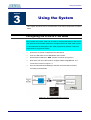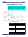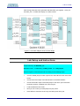
1
Altera DE2 Board
Development and Education Board
Getting Started Guide
DE2 Board
Document Version 1.2
Preliminary Version
OCT. 02, 2005 by Terasic
© 2005 by Altera
Altera DE2 Board
Page Index
CHAPTER 1 ABOUT THE KIT...................................................................................................................................... 1
1-1 KIT CONTENTS ........................................................................................................................................................ 1
1-2 ASSEMBLE THE RUBBER FEET ................................................................................................................................ 2
1-3 GETTING HELP ........................................................................................................................................................ 3
CHAPTER 2 ALTERA DE2 BOARD ............................................................................................................................ 4
2-1 THE DE2 BOARD..................................................................................................................................................... 4
2-2 EXAMINE THE BOARD .............................................................................................................................................. 4
2-3 FEATURES ............................................................................................................................................................... 5
2-4 DE2 BLOCK DIAGRAM ............................................................................................................................................ 6
2-5 DE2 BLOCK DESCRIPTION...................................................................................................................................... 7
2-6 POWER UP THE BOARD TO SEE THE DEMO ......................................................................................................... 10
CHAPTER 3 USING THE SYSTEM ........................................................................................................................... 12
3-1 CONFIGURING THE FPGA IN JTGA MODE ........................................................................................................... 12
3-2 CONFIGURING THE FPGA IN AS MODE ................................................................................................................ 13
3-3 CONTROLLING THE DE2 USING TERASIC LINK ..................................................................................................... 14
3-4 XSGA OUTPUT ..................................................................................................................................................... 14
3-5 24-BIT AUDIO CODEC ......................................................................................................................................... 17
3-6 USING THE LEDS AND SWITCHES......................................................................................................................... 18
3-7 USING THE 7-SEG DISPLAYS AND LCD MODULE ................................................................................................ 21
3-8 USING THE EXPANSION HEADERS ........................................................................................................................ 24
3-9 USING THE SERIAL PORTS(RS232) ..................................................................................................................... 26
3-10 USING THE SERIAL PORTS(PS/2)....................................................................................................................... 27
3-11 USING THE FAST ETHERNET NETWORK CONTROLLER ...................................................................................... 28
3-12 USING TV DECODER........................................................................................................................................... 29
3-13 IMPLEMENTING A TV ENCODER .......................................................................................................................... 31
3-14 USING USB HOST/DEVICE ................................................................................................................................. 31
3-15 USING IRDA ........................................................................................................................................................ 33
3-16 USING SDRAM/SRAM/FLASH .......................................................................................................................... 33
CHAPTER 4 SOFTWARE INSTALLATION .............................................................................................................. 33
4-1 INSTALL QUARTUS II.............................................................................................................................................. 33
4-2 CONNECTING THE USB CABLE TO THE BOARD - USB BLASTER INSTALLATION ................................................. 33
4-3 POTENTIAL PROBLEMS AND W ORKAROUND FOR USING USB BLASTER ............................................................. 33
4-4 INSTALL DE2 LAB CD-ROM................................................................................................................................. 33
4-5 THE TOP-LEVEL VERILOG MODULE AND PIN ASSIGNMENT .................................................................................. 33
CHAPTER 5 FIRST LAB: DE2 TOP-LEVEL AND DEFAULT BITSTREAM ....................................................... 33
ii
Altera DE2 Board
5-1 POWER UP THE BOARD ........................................................................................................................................ 33
5-2 THE TOP-LEVEL VERILOG MODULE IN CYCLONE II .............................................................................................. 33
5-3 COMPILING THE DESIGN ....................................................................................................................................... 33
5-4 DOWNLOAD BITSTREAM ........................................................................................................................................ 33
CHAPTER 6 LAB 2: TV BOX...................................................................................................................................... 33
6-1 LAB SETUP AND INSTRUCTIONS ............................................................................................................................ 33
CHAPTER 7 LAB 3: USB PAINT BRUSH ................................................................................................................ 33
7-1 LAB SETUP AND INSTRUCTIONS ............................................................................................................................ 33
CHAPTER 8 LAB 4: USB DEVICE ............................................................................................................................ 33
8-1 LAB SETUP AND INSTRUCTIONS ............................................................................................................................ 33
CHAPTER 9 LAB 5: A KARAOKE MACHINE ......................................................................................................... 33
9-1 LAB SETUP AND INSTRUCTIONS ............................................................................................................................ 33
CHAPTER 10 LAB 6: ETHERNET PACKET SENDING/RECEIVING.................................................................. 33
10-1 LAB SETUP AND INSTRUCTIONS .......................................................................................................................... 33
CHAPTER 11 LAB 7: DE2 CONTROL PANEL ........................................................................................................ 33
11-1 LAB SETUP AND INSTRUCTIONS .......................................................................................................................... 33
11-2 CONTROL THE BOARD USING DE2 CONTROL PANEL ........................................................................................ 33
11-3 THE FLASH PROGRAMMER ................................................................................................................................. 33
11-4 THE SDRAM / SRAM CONTROLLER AND PROGRAMMER ................................................................................. 33
11-5 PS/2 AND 7-SEG DISPLAY CONTROL ................................................................................................................ 33
11-6 TOOLS - MULTI-PORT SRAM/SDRAM/FLASH CONTROLLER ......................................................................... 33
11-7 VGA DISPLAY CONTROL PANEL – DISPLAY DEFAULT IMAGE ............................................................................. 33
11-8 VGA DISPLAY CONTROL PANEL – DISPLAY USER’S OWN IMAGE ...................................................................... 33
11-9 HOW TO PREPARE YOUR OWN IMAGE DATA ...................................................................................................... 33
11-10 BOARD SELF TESTER ....................................................................................................................................... 33
CHAPTER 12 LAB 8: SD CARD MUSIC PLAYER.................................................................................................. 33
12-1 LAB SETUP AND INSTRUCTIONS .......................................................................................................................... 33
CHAPTER 13 APPENDIX ............................................................................................................................................ 33
13-1 REVISION HISTORY ............................................................................................................................................. 33
13-2 SCHEMATIC ......................................................................................................................................................... 33
13-3 ALWAYS VISIT DE2 W EBPAGE FOR NEW LABS .................................................................................................. 33
iii
About the Kit
Chapter
Chapter 1
1
About the Kit
The DE2 Kit provides everything you need to develop many advanced digital
designs using Altera Cyclone || device. The Getting Started User Guide is written
in a way to enable users to walk through many reference designs in 30 minutes.
This chapter provides users key information about the kit.
Kit Contents
1-1
Figure 1.1 shows the photo of the DE2 package. The DE2 Kit includes:
The DE2 Board.
USB Cable for FPGA programming and control.
DE2 Lab CD-ROM containing DE2 Control Panel, reference designs, 3
rd
party specs, software tools, and this User Guide.
Altera Quartus II 5.0 Web Edition CD-ROM and Nios II 5.0 CD-ROM
A bag of copper stands, screw, and rubber feet.
A piece of Plexiglas assembled with the board.
9V DC Wall-mount power supply.
1
About the Kit
Figure 1.1. The DE2 Kit Package Content
Assemble the Rubber Feet
1-2
Users can use the attached bag of copper stands, silicon feet cover, and screw to
create suitable feet according to users’s own applications
Assemble a screw, a copper stand, and a rubber (silicon) cover as shown in
Figure 1.2 for each of the 6 screw holes on DE2.
Assemble the plexiglass cover attached if extra protection is desired.
2
About the Kit
Figure 1.2 The Rubber Feet Set
Getting Help
1-3
Here are some places to get help if you encounter any problem:
Email to [email protected]
Taiwan & China: +886-3-550-8800
Korea & Japan: +82-2-512-7661
3
Altera DE2 Board
Chapter
Chapter 2
2
Altera DE2 Board
This chapter will walk you through each part of your DE2 board to illustrate the
features equipped.
The DE2 Board
2-1
The DE2 board is designed using the same strict design and layout practices
used in high-end volume production products such as high-density PC
motherboards and car infotainment systems with the highest QC standard. Major
design and layout considerations are listed below:
Layout traces and components are carefully arranged so that they are properly
aligned. This nice alignment will increase the yield for manufacturing and ease
board debugging procedure.
Jumper-free design for robustness. Jumpers are a great point of failure and might
cause frustration for users who don’t keep the manuals with them all the time.
Components’ selection was made according to the volume shipped. We selected
the most common component configuration used in PC and DVD players to
ensure the continuous supply of the component resource in the future.
Protection on Power and IOs are considered to cover most of the accidental
cases in the field.
Examine the Board
2-2
Examine your board with the following diagram in Figure 2.1.
4
Altera DE2 Board
Figure 2.1. DE2 Development Board Components & Interfaces
Features
2-3
DE2 board provides users many features to enable various multimedia project
development. Component selection was made according to the most popular
design in volume production multimedia products such as DVD, VCD, and MP3
players. The DE2 platform allows users to quickly understand all the insight tricks
to design real multimedia projects for industry.
Altera Cyclone II 2C35 FPGA with 35000 LEs
Altera Serial Configuration deivices (EPCS16) for Cyclone II 2C35
USB Blaster built in on board for programming and user API controlling
JTAG Mode and AS Mode are supported
8Mbyte (1M x 4 x 16) SDRAM
1Mbyte Flash Memory (upgradeable to 4Mbyte)
SD Card Socket
4 Push-button switches
18 DPDT switches
9 Green User LEDs
5
Altera DE2 Board
18 Red User LEDs
50MHz Oscillator and 27MHz Oscillator for external clock sources
24-bit CD-Quality Audio CODEC with line-in, line-out, and microphone-in
jacks
VGA DAC (10-bit high-speed triple ADCs) with VGA out connector
TV Decoder (NTSC/PAL) and TV in connector
10/100 Ethernet Controller with socket.
USB Host/Slave Controller with USB type A and type B connectors.
RS-232 Transceiver and 9-pin connector
PS/2 mouse/keyboard connector
IrDA transceiver
Two 40-pin Expansion Headers with diode protection
DE2 Lab CD-ROM which contains many examples with source code to
exercise the boards, including: SDRAM and Flash Controller, CD-Quality
Music Player, VGA and TV Labs, SD Card reader, RS-232/PS-2
Communication Labs, NIOSII, and Control Panel API
DE2 Block Diagram
2-4
Figure 2.2 shos a block diagram of the DE2 Board. The most recent
documentation for system can be obtained from the DE2 support website at:
http://de2.terasic.com
6
Altera DE2 Board
Figure 2.2. Block Diagram of DE2 Board
DE2 Block Description
2-5
CYCLONE II 2C35 FPGA
With 35000 LEs
FineLine BGA 672-pin package
475 User IOs
With 105 M4K RAM Blocks and 483Kbit SRAM
With 35 embedded multipliers and 4 PLLs
Altera Serial Configuration device (EPCS16) and USB Blaster Circuit
USB Blaster built in on board for programming and user API controlling
JTAG Mode and AS Mode are supported
Provides EPCS16 Serial Configuration device
8Mbyte SDRAM
Single Data Rate Synchronous Dynamic RAM memory chip
Organized as 1M x 4 x 16 bit.
Support access through both NIOS II and Terasic high-speed Multi-port
SDRAM Controller
1Mbyte Flash Memory (upgradeable to 4Mbyte)
Equipped with 1Mbyte NAND Flash memory
Layout is designed to support up to 4Mbye SDRAM
8-bit data bus
Support access through both NIOS II and Terasic multi-port Flash
Controller
SD Card Socket
Provides SPI mode for SD Card access
Support access through NIOS II with Terasic SD Card Driver
Push-button Switches
7
Altera DE2 Board
With 4 push-button switches
Debounced by Schimitter trigger
Normal high and Generate one active-low pulse when the switch is pushed
DPDT Switches
Contains 18 DPDT Switches for user inputs.
Clock Inputs
Contains a 50MHz Oscillator
Contains a 27MHz Oscillator
Contains a SMA External Clock Input
Audio CODEC
Uses Wolfson WM8731 24-bit sigma-delta Best-Quality Audio CODEC
Contains line-level input, line-level output, and microphone input jacks
Sampling frequency: 8Khz – 96Khz
Applications for MP3 players and recorders, PDAs, smart phones.
XSGA DAC Output
Uses ADI 7123 240Mhz Triple 10-bit High-speed Video DAC
With 15-pin high-density D-sub connector
Supports up to 1600x1200 at 100Hz refresh rate – best performance and
quality provided.
Can be used to implement a high-performance TV Encoder together with
Cyclone II FPGA.
NTSC/PAL TV Decoder Circuit
Uses ADI 7181B Multi-format SDTV Video Decoder
Support NTSC-(M,J,4.43), PAL-(B/D/G/H/I/M/N), SECAM.
Integrates three 54Mhz, 9-bit ADCs
Clocked from a single 27-Mhz oscillator input
Multiple programmable analog input formats: Composite video (CVBS),
S-Video(Y/C), and YPrPb components.
Supports digital output formats (8-bit/16-bit): ITU-R BT.656 YCrCb 4:2:2
output + HS, VS, and FIELD.
Applications: DVD recorders, LCD TVs, Set-top boxes, Digital TV, Portable
8
Altera DE2 Board
video devices.
10/100 Ethernet Controller
Integrated MAC and PHY with a general processor interface
Supports 100Base-T and 10Base-T applications.
Supports full duplex operation at 10Mb/s and 100Mb/s, with auto-MDIX
Fully compliant with the IEEE 802.3u Spec
Supports IP/TCP/UDP checksum generation and checking
Supports back pressure mode for half-duplex mode flow control
USB Host/Slave Controller
Complies fully with Universal Serial Bus Specification Rev. 2.0
Supports data transfer at full-speed and low-speed
Supports both USB Host and Device
Supports two USB ports (One type A for host and one type B for device on
DE2)
Provides high-speed parallel interface to most CPUs available. Supports
NIOS II Core with driver now (implemented by Terasic)
Supports Programmed I/O (PIO) or Direct Memory Access (DMA)
Serial Ports
Provides two serial ports: one RS-232 port and one PS/2 port.
Provides DB-9 serial connector for the RS-232 port
Provides PS/2 connector for connecting a PS2 mouse or keyboard to DE2
IrDA transceiver
Contains a 115.2kb/s Infrared Transceiver
32 mA LED Drive Current
Integrated EMI Shield
IEC825-1 Class 1 Eye Safe
Edge Detection Input
Two 40-pin Expansion Headers with diode protection
A total of 72 Cyclone II I/O pins are brought out to two 40-pin expansion
connectors.
The 40-pin header is designed to accept a standard 40-pin ribbon cable
9
Altera DE2 Board
used for a standard IDE device.
USB Blaster Circuits and Configuration Devices
Built-in USB Blaster circuits on board with enhanced features to provide
DE2 Control Panel API Link.
Provide both JTAG and AS mode programming mode
Contains a 16Mbit (EPCS16) serial configuration device
Power Up the Board to See the Demo
2-6
DE2 board comes with a preloaded bitstream to demostrate some features of the
board. This bitstream also allows users to check if the board is working properly in
seconds. Perform the following steps:
1.
Connect the USB cable from PC to your DE2 board
2.
Connect the 9V adapter cable to the DE2 board
3.
Connect your LCD Monitor to your DE2.
4.
Connect your headset to your DE2.
5.
Press the Power ON/OFF Switch on DE2
6.
Make sure the [RUN<->PROG] switch is set to RUN position (Note that
PROG position is only used for AS Mode programming). Please refer to
Figure 2.2.
Figure 2.2. JTAG/Operation (RUN) mode and AS Mode (PROG) switch settting.
What you should see and hear
All user LEDs are flashing.
All the 7-SEG displays are cycling through 0-F.
The LCD display shows “Welcome to the Altera DE2 Board”.
LCD Monitor displays a color pattern shown in Figure 2.3.
Switch SW17 position to OFF (down), you should hear a 1-khz sound.
Switch SW17 position to ON(up) and connect the output of a MP3 player
to the line-in connector of the DE2 board, you should hear the music from
your headset if you play music from your MP3 player (or PC/iPod).
You can also connect your microphone to the MIC connector of the DE2
10
Altera DE2 Board
board. Your voice will be mixed with the music played from the MP3
player.
Figure 2.3 The default VGA Output Pattern
11
Using the System
Chapter
Chapter 3
3
Using the System
This chapter describes how to work with each of the major components on DE2 in
detail.
Configuring the FPGA in JTGA Mode
3-1
DE2 provides users both JTAG and AS mode to download bitstream to the FPGA.
The first and recommended method is to configure FPGA via JTAG mode. Figure
3.1 describes the block diagram of the JTAG programming method. Follow the
steps below to program the FPGA:
Ensure the 9V power is supplied to the DE2 Board.
Connect USB Cable to the USB Blaster Port of DE2.
Set the Switch (SW19) to “RUN” position, as shown in Figure 3.2.
Now users can use JTGA mode to configure FPGA using SOF file. The
connection is shown in Figure 3.1.
Once the bitstream downloading is finished, the FPGA start to behave
according to the bistream.
Figure 3.1. The JTAG configuration scheme
12
Using the System
Figure 3.2 Set SW19 to RUN position for JTAG programming and normal
operation
Configuring the FPGA in AS Mode
3-2
The bitstream can be downloaded via Active Serial Programming mode (AS
mode). By default, the switch is set to the position of RUN for JTAG mode so that
the SOF bistream file is downloaded directly to the FPGA chip. AS Mode, where
POF bitstream is downloaded directly to the Flash-based Serial Configuration
device, should be used only when the design is finalized or the design has to be
tested without a PC. Set the switch to PROG for AS mode. Note that the switch
position should be kept at RUN position for normal operation. Figure 3.3 shows the
AS mode connection scheme. Perform the following steps to program in AS mode:
Ensure the 9V power is supplied to DE2 Board.
Connect USB Cable to the USB Blaster Port of DE2.
Set the Switch (SW19) to “PROG” position.
Now users can use AS mode to configure FPGA using POF file. The
connection is shown in Figure 3.3.
Once the POF bitstream downloading is finished, you need to set the SW19
back to “RUN” position and reset (turn off and turn on) the power so that the
bistream can be loaded into FPGA from the Serial Configuration Device.
Figure 3.3 The connection and SW19 setup for AS mode programming
13
Using the System
Controlling the DE2 using Terasic Link
3-3
We designed a special link from MAX 3128 to FPGA’s user IO pins to enable users
to control the FPGA from PC using our own command set. Figure 3.4 shows the
connection scheme of the Terasic Link.
User can refer to Chapter 11 to exercise the DE2 Control Panel which uses
Terasic Link/IP to control the board.
DE2 Control Panel shares the same link of JTAG and NIOS II IDE control
lines – user can use ONLY one of the three links at any given time.
Figure 3.4 The Terasic Link is used to allow the software in PC side to
communicate with the API IP core inside the FPGA
XSGA Output
3-4
ADV7123 from Analog Devices is used for the 10-bit D/A conversion for video
signals. The converted signals are then connected to the 15-pin D-Sub connector
for output to VGA. The XSGA circuits can support up to 1600x1200 @ 100Hz.
Please refer to XSGA timing spec to design FPGA to avoid any problems when
connecting to real devices. For detailed information on how to use the LCD module,
users can refer to the spec under C:\DE2\Datasheet\VGA DAC
User can refer to Figure 3.5 for the basic VGA timing:
14
Using the System
Figure 3.5 VGA Display Horizontal timing spec
Both Horizontal and Vertical timing periods can be divided into four zones:
H-Sync (a), back porch (b), front porch (d), and display interval(c).
Refer to Figure 3.6 for detailed VGA timing spec on the four timing zones.
Refer to Table 3.1 for the pin assignment of the associated interface.
VGA mode
Horizontal Timing Spec
Configuration
Resolution(HxV)
a(us)
b(us)
c(us)
d(us)
Pixel clock(Mhz)
VGA(60Hz)
640x480
3.8
1.9
25.4
0.6
25
(640/c)
VGA(85Hz)
640x480
1.6
2.2
17.8
1.6
36
(640/c)
SVGA(60Hz)
800x600
3.2
2.2
20
1
40
(800/c)
SVGA(75Hz)
800x600
1.6
3.2
16.2
0.3
49
(800/c)
SVGA(85Hz)
800x600
1.1
2.7
14.2
0.6
56
(800/c)
XGA(60Hz)
1024x768
2.1
2.5
15.8
0.4
65
(1024/c)
XGA(70Hz)
1024x768
1.8
1.9
13.7
0.3
75
(1024/c)
XGA(85Hz)
1024x768
1.0
2.2
10.8
0.5
95
(1024/c)
1280x1024(60Hz)
1280x1024
1.0
2.3
11.9
0.4
108
(1280/c)
.
VGA mode
Vertical Timing Spec
Configuration
Resolution(HxV)
a(lines)
b(lines)
c(lines)
d(lines)
VGA(60Hz)
640x480
2
33
480
10
VGA(85Hz)
640x480
3
25
480
1
SVGA(60Hz)
800x600
4
23
600
1
SVGA(75Hz)
800x600
3
21
600
1
SVGA(85Hz)
800x600
3
27
600
1
XGA(60Hz)
1024x768
6
29
768
3
XGA(70Hz)
1024x768
6
29
768
3
XGA(85Hz)
1024x768
3
36
768
1
1280x1024(60Hz)
1280x1024
3
38
1024
1
Figure 3.6 VGA Display Detailed Timing Spec
15
Using the System
Signal Name
FPGA Pin No.
Description
VGA_R[0]
PIN_C8
VGA Red[0]
VGA_R[1]
PIN_F10
VGA Red[1]
VGA_R[2]
PIN_G10
VGA Red[2]
VGA_R[3]
PIN_D9
VGA Red[3]
VGA_R[4]
PIN_C9
VGA Red[4]
VGA_R[5]
PIN_A8
VGA Red[5]
VGA_R[6]
PIN_H11
VGA Red[6]
VGA_R[7]
PIN_H12
VGA Red[7]
VGA_R[8]
PIN_F11
VGA Red[8]
VGA_R[9]
PIN_E10
VGA Red[9]
VGA_G[0]
PIN_B9
VGA Green[0]
VGA_G[1]
PIN_A9
VGA Green[1]
VGA_G[2]
PIN_C10
VGA Green[2]
VGA_G[3]
PIN_D10
VGA Green[3]
VGA_G[4]
PIN_B10
VGA Green[4]
VGA_G[5]
PIN_A10
VGA Green[5]
VGA_G[6]
PIN_G11
VGA Green[6]
VGA_G[7]
PIN_D11
VGA Green[7]
VGA_G[8]
PIN_E12
VGA Green[8]
VGA_G[9]
PIN_D12
VGA Green[9]
VGA_B[0]
PIN_J13
VGA Blue[0]
VGA_B[1]
PIN_J14
VGA Blue[1]
VGA_B[2]
PIN_F12
VGA Blue[2]
VGA_B[3]
PIN_G12
VGA Blue[3]
VGA_B[4]
PIN_J10
VGA Blue[4]
VGA_B[5]
PIN_J11
VGA Blue[5]
VGA_B[6]
PIN_C11
VGA Blue[6]
VGA_B[7]
PIN_B11
VGA Blue[7]
VGA_B[8]
PIN_C12
VGA Blue[8]
VGA_B[9]
PIN_B12
VGA Blue[9]
VGA_CLK
PIN_B8
VGA Clock
VGA_BLANK
PIN_D6
VGA BLANK
VGA_HS
PIN_A7
VGA H_SYNC
VGA_VS
PIN_D8
VGA V_SYNC
VGA_SYNC
PIN_B7
VGA SYNC
Table 3.1 Pin Assignment for VGA
16
Using the System
24-bit Audio CODEC
3-5
WM8731 is used to implement the 24-bit Audio CODEC on DE2. This chip provides
Microphone in, Line In, and Line Out connectors. The sample rate is adjustable from
8Khz to 96Khz by using the I2C bus on DE2 board. For detailed information on how to
use the audio CODEC, users can refer to the spec under C:\DE2\Datasheet\Audio
CODEC.
Figure 3.7 shows the circuit diagram of the audio part of DE2. The pin assignment of
the associated interface is shown in Table 3.2.
Figure 3.7 24-bit Audio DAC
Signal Name
FPGA Pin No.
Description
AUD_ADCLRCK
PIN_C5
Audio CODEC ADC LR Clock
AUD_ADCDAT
PIN_B5
Audio CODEC ADC Data
AUD_DACLRCK
PIN_C6
Audio CODEC DAC LR Clock
AUD_DACDAT
PIN_A4
Audio CODEC DAC Data
AUD_XCK
PIN_A5
Audio CODEC Chip Clock
AUD_BCLK
PIN_B4
Audio CODEC Bit-Stream Clock
I2C_SCLK
PIN_A6
I2C Data
I2C_SDAT
PIN_B6
I2C Clock
17
Using the System
Table 3.2 Pin Assignment for Audio CODEC
Using the LEDs and Switches
3-6
The DE2 Board provides 4 push buttons. All of the buttons are Schmitt Trigger
de-bounced. When a push button is pressed, only one zero pulse will be generated.
There are also 18 toggle switches on the DE2 boards for users to set HIGH/LOW to
the 18 GPIOs of the CycloneII FPGA. The DE2 Board has 9 green user LEDs and 18
red user LEDs. Figure 3.8 shows the related schematics. The pin assignments of the
push buttons, DPDT switches, and LEDs are listed in Table 3.3, 3.4, and 3.5,
respectively.
18
Using the System
Figure 3.8 Push Buttons, Toggle Switches, and LEDs
Signal Name
FPGA Pin No.
Description
SW[0]
PIN_N25
DPDT Switch[0]
SW[1]
PIN_N26
DPDT Switch[1]
SW[2]
PIN_P25
DPDT Switch[2]
SW[3]
PIN_AE14
DPDT Switch[3]
SW[4]
PIN_AF14
DPDT Switch[4]
SW[5]
PIN_AD13
DPDT Switch[5]
SW[6]
PIN_AC13
DPDT Switch[6]
SW[7]
PIN_C13
DPDT Switch[7]
SW[8]
PIN_B13
DPDT Switch[8]
SW[9]
PIN_A13
DPDT Switch[9]
SW[10]
PIN_N1
DPDT Switch[10]
SW[11]
PIN_P1
DPDT Switch[11]
SW[12]
PIN_P2
DPDT Switch[12]
SW[13]
PIN_T7
DPDT Switch[13]
SW[14]
PIN_U3
DPDT Switch[14]
SW[15]
PIN_U4
DPDT Switch[15]
SW[16]
PIN_V1
DPDT Switch[16]
SW[17]
PIN_V2
DPDT Switch[17]
Table 3.3 Pin Assignment for DPDT Switches
19
Using the System
Signal Name
FPGA Pin No.
Description
KEY[0]
PIN_G26
Push Button[0]
KEY[1]
PIN_N23
Push Button[1]
KEY[2]
PIN_P23
Push Button[2]
KEY[3]
PIN_W26
Push Button[3]
Table 3.4 Pin Assignment for Push Buttoms
Signal Name
FPGA Pin No.
Description
LEDR[0]
PIN_AE23
LED Red[0]
LEDR[1]
PIN_AF23
LED Red[1]
LEDR[2]
PIN_AB21
LED Red[2]
LEDR[3]
PIN_AC22
LED Red[3]
LEDR[4]
PIN_AD22
LED Red[4]
LEDR[5]
PIN_AD23
LED Red[5]
LEDR[6]
PIN_AD21
LED Red[6]
LEDR[7]
PIN_AC21
LED Red[7]
LEDR[8]
PIN_AA14
LED Red[8]
LEDR[9]
PIN_Y13
LED Red[9]
LEDR[10]
PIN_AA13
LED Red[10]
LEDR[11]
PIN_AC14
LED Red[11]
LEDR[12]
PIN_AD15
LED Red[12]
LEDR[13]
PIN_AE15
LED Red[13]
LEDR[14]
PIN_AF13
LED Red[14]
LEDR[15]
PIN_AE13
LED Red[15]
LEDR[16]
PIN_AE12
LED Red[16]
LEDR[17]
PIN_AD12
LED Red[17]
LEDG[0]
PIN_AE22
LED Green[0]
LEDG[1]
PIN_AF22
LED Green[1]
LEDG[2]
PIN_W19
LED Green[2]
LEDG[3]
PIN_V18
LED Green[3]
LEDG[4]
PIN_U18
LED Green[4]
LEDG[5]
PIN_U17
LED Green[5]
LEDG[6]
PIN_AA20
LED Green[6]
LEDG[7]
PIN_Y18
LED Green[7]
LEDG[8]
PIN_Y12
LED Green[8]
Table 3.5 Pin Assignment for LEDs
20
Using the System
Using the 7-SEG Displays and LCD Module
3-7
The DE2 Board has eight 7-SEG displays and one 16x2 LCD module. The LCD
module has built-in font library; users have to send control signals according to its
specific timing to display desired characters at the correct location. For detailed
information on how to use the LCD module, users can refer to the spec under
C:\DE2\Datasheet\LCD
Figure 3.9 shows the related schematics. The pin assignments of the 7-SEG displays,
and 16x2 LCD Module are listed in Table 3.6 and 3.7, respectively.
Figure 3.9 7-SEG Display and 16x2 LCD module
21
Using the System
Signal Name
FPGA Pin No.
Description
HEX0[0]
PIN_AF10
Seven Segment Digital 0[0]
HEX0[1]
PIN_AB12
Seven Segment Digital 0[1]
HEX0[2]
PIN_AC12
Seven Segment Digital 0[2]
HEX0[3]
PIN_AD11
Seven Segment Digital 0[3]
HEX0[4]
PIN_AE11
Seven Segment Digital 0[4]
HEX0[5]
PIN_V14
Seven Segment Digital 0[5]
HEX0[6]
PIN_V13
Seven Segment Digital 0[6]
HEX1[0]
PIN_V20
Seven Segment Digital 1[0]
HEX1[1]
PIN_V21
Seven Segment Digital 1[1]
HEX1[2]
PIN_W21
Seven Segment Digital 1[2]
HEX1[3]
PIN_Y22
Seven Segment Digital 1[3]
HEX1[4]
PIN_AA24
Seven Segment Digital 1[4]
HEX1[5]
PIN_AA23
Seven Segment Digital 1[5]
HEX1[6]
PIN_AB24
Seven Segment Digital 1[6]
HEX2[0]
PIN_AB23
Seven Segment Digital 2[0]
HEX2[1]
PIN_V22
Seven Segment Digital 2[1]
HEX2[2]
PIN_AC25
Seven Segment Digital 2[2]
HEX2[3]
PIN_AC26
Seven Segment Digital 2[3]
HEX2[4]
PIN_AB26
Seven Segment Digital 2[4]
HEX2[5]
PIN_AB25
Seven Segment Digital 2[5]
HEX2[6]
PIN_Y24
Seven Segment Digital 2[6]
HEX3[0]
PIN_Y23
Seven Segment Digital 3[0]
HEX3[1]
PIN_AA25
Seven Segment Digital 3[1]
HEX3[2]
PIN_AA26
Seven Segment Digital 3[2]
HEX3[3]
PIN_Y26
Seven Segment Digital 3[3]
HEX3[4]
PIN_Y25
Seven Segment Digital 3[4]
HEX3[5]
PIN_U22
Seven Segment Digital 3[5]
HEX3[6]
PIN_W24
Seven Segment Digital 3[6]
HEX4[0]
PIN_U9
Seven Segment Digital 4[0]
HEX4[1]
PIN_U1
Seven Segment Digital 4[1]
HEX4[2]
PIN_U2
Seven Segment Digital 4[2]
HEX4[3]
PIN_T4
Seven Segment Digital 4[3]
HEX4[4]
PIN_R7
Seven Segment Digital 4[4]
HEX4[5]
PIN_R6
Seven Segment Digital 4[5]
HEX4[6]
PIN_T3
Seven Segment Digital 4[6]
HEX5[0]
PIN_T2
Seven Segment Digital 5[0]
HEX5[1]
PIN_P6
Seven Segment Digital 5[1]
22
Using the System
HEX5[2]
PIN_P7
Seven Segment Digital 5[2]
HEX5[3]
PIN_T9
Seven Segment Digital 5[3]
HEX5[4]
PIN_R5
Seven Segment Digital 5[4]
HEX5[5]
PIN_R4
Seven Segment Digital 5[5]
HEX5[6]
PIN_R3
Seven Segment Digital 5[6]
HEX6[0]
PIN_R2
Seven Segment Digital 6[0]
HEX6[1]
PIN_P4
Seven Segment Digital 6[1]
HEX6[2]
PIN_P3
Seven Segment Digital 6[2]
HEX6[3]
PIN_M2
Seven Segment Digital 6[3]
HEX6[4]
PIN_M3
Seven Segment Digital 6[4]
HEX6[5]
PIN_M5
Seven Segment Digital 6[5]
HEX6[6]
PIN_M4
Seven Segment Digital 6[6]
HEX7[0]
PIN_L3
Seven Segment Digital 7[0]
HEX7[1]
PIN_L2
Seven Segment Digital 7[1]
HEX7[2]
PIN_L9
Seven Segment Digital 7[2]
HEX7[3]
PIN_L6
Seven Segment Digital 7[3]
HEX7[4]
PIN_L7
Seven Segment Digital 7[4]
HEX7[5]
PIN_P9
Seven Segment Digital 7[5]
HEX7[6]
PIN_N9
Seven Segment Digital 7[6]
Table 3.6 Pin Assignment for 7-SEG Display
Signal Name
FPGA Pin No.
Description
LCD_DATA[0]
PIN_J1
LCD Data[0]
LCD_DATA[1]
PIN_J2
LCD Data[1]
LCD_DATA[2]
PIN_H1
LCD Data[2]
LCD_DATA[3]
PIN_H2
LCD Data[3]
LCD_DATA[4]
PIN_J4
LCD Data[4]
LCD_DATA[5]
PIN_J3
LCD Data[5]
LCD_DATA[6]
PIN_H4
LCD Data[6]
LCD_DATA[7]
PIN_H3
LCD Data[7]
LCD_RW
PIN_K4
LCD Read/Write Select, 0 = Write, 1 = Read
LCD_EN
PIN_K3
LCD Enable
LCD_RS
PIN_K1
LCD Command/Data Select, 0 = Command, 1 = Data
LCD_ON
PIN_L4
LCD Power ON/OFF
LCD_BLON
PIN_K2
LCD Back Light ON/OFF
Table 3.7 Pin Assignment for 16x2 LCD Module
23
Using the System
Using the Expansion Headers
3-8
The DE2 Board provides users two 40-pin expansion headers. Each header
provides DC +5V (VCC5), DC +3.3V (VCC33), two GND pins for users to build
their own daughter cards using the DE2 expansion ports.
Figure 3.10 shows the related schematics. The pin assignment of the associated
interface is shown in Table 3.8.
Figure 3.10 Two 40-pin Expansion Headers
Signal Name
FPGA Pin No.
Description
GPIO_0[0]
PIN_D25
GPIO Connection 0[0]
GPIO_0[1]
PIN_J22
GPIO Connection 0[1]
GPIO_0[2]
PIN_E26
GPIO Connection 0[2]
GPIO_0[3]
PIN_E25
GPIO Connection 0[3]
GPIO_0[4]
PIN_F24
GPIO Connection 0[4]
GPIO_0[5]
PIN_F23
GPIO Connection 0[5]
GPIO_0[6]
PIN_J21
GPIO Connection 0[6]
GPIO_0[7]
PIN_J20
GPIO Connection 0[7]
24
Using the System
GPIO_0[8]
PIN_F25
GPIO Connection 0[8]
GPIO_0[9]
PIN_F26
GPIO Connection 0[9]
GPIO_0[10]
PIN_N18
GPIO Connection 0[10]
GPIO_0[11]
PIN_P18
GPIO Connection 0[11]
GPIO_0[12]
PIN_G23
GPIO Connection 0[12]
GPIO_0[13]
PIN_G24
GPIO Connection 0[13]
GPIO_0[14]
PIN_K22
GPIO Connection 0[14]
GPIO_0[15]
PIN_G25
GPIO Connection 0[15]
GPIO_0[16]
PIN_H23
GPIO Connection 0[16]
GPIO_0[17]
PIN_H24
GPIO Connection 0[17]
GPIO_0[18]
PIN_J23
GPIO Connection 0[18]
GPIO_0[19]
PIN_J24
GPIO Connection 0[19]
GPIO_0[20]
PIN_H25
GPIO Connection 0[20]
GPIO_0[21]
PIN_H26
GPIO Connection 0[21]
GPIO_0[22]
PIN_H19
GPIO Connection 0[22]
GPIO_0[23]
PIN_K18
GPIO Connection 0[23]
GPIO_0[24]
PIN_K19
GPIO Connection 0[24]
GPIO_0[25]
PIN_K21
GPIO Connection 0[25]
GPIO_0[26]
PIN_K23
GPIO Connection 0[26]
GPIO_0[27]
PIN_K24
GPIO Connection 0[27]
GPIO_0[28]
PIN_L21
GPIO Connection 0[28]
GPIO_0[29]
PIN_L20
GPIO Connection 0[29]
GPIO_0[30]
PIN_J25
GPIO Connection 0[30]
GPIO_0[31]
PIN_J26
GPIO Connection 0[31]
GPIO_0[32]
PIN_L23
GPIO Connection 0[32]
GPIO_0[33]
PIN_L24
GPIO Connection 0[33]
GPIO_0[34]
PIN_L25
GPIO Connection 0[34]
GPIO_0[35]
PIN_L19
GPIO Connection 0[35]
GPIO_1[0]
PIN_K25
GPIO Connection 1[0]
GPIO_1[1]
PIN_K26
GPIO Connection 1[1]
GPIO_1[2]
PIN_M22
GPIO Connection 1[2]
GPIO_1[3]
PIN_M23
GPIO Connection 1[3]
GPIO_1[4]
PIN_M19
GPIO Connection 1[4]
GPIO_1[5]
PIN_M20
GPIO Connection 1[5]
GPIO_1[6]
PIN_N20
GPIO Connection 1[6]
GPIO_1[7]
PIN_M21
GPIO Connection 1[7]
GPIO_1[8]
PIN_M24
GPIO Connection 1[8]
GPIO_1[9]
PIN_M25
GPIO Connection 1[9]
25
Using the System
GPIO_1[10]
PIN_N24
GPIO Connection 1[10]
GPIO_1[11]
PIN_P24
GPIO Connection 1[11]
GPIO_1[12]
PIN_R25
GPIO Connection 1[12]
GPIO_1[13]
PIN_R24
GPIO Connection 1[13]
GPIO_1[14]
PIN_R20
GPIO Connection 1[14]
GPIO_1[15]
PIN_T22
GPIO Connection 1[15]
GPIO_1[16]
PIN_T23
GPIO Connection 1[16]
GPIO_1[17]
PIN_T24
GPIO Connection 1[17]
GPIO_1[18]
PIN_T25
GPIO Connection 1[18]
GPIO_1[19]
PIN_T18
GPIO Connection 1[19]
GPIO_1[20]
PIN_T21
GPIO Connection 1[20]
GPIO_1[21]
PIN_T20
GPIO Connection 1[21]
GPIO_1[22]
PIN_U26
GPIO Connection 1[22]
GPIO_1[23]
PIN_U25
GPIO Connection 1[23]
GPIO_1[24]
PIN_U23
GPIO Connection 1[24]
GPIO_1[25]
PIN_U24
GPIO Connection 1[25]
GPIO_1[26]
PIN_R19
GPIO Connection 1[26]
GPIO_1[27]
PIN_T19
GPIO Connection 1[27]
GPIO_1[28]
PIN_U20
GPIO Connection 1[28]
GPIO_1[29]
PIN_U21
GPIO Connection 1[29]
GPIO_1[30]
PIN_V26
GPIO Connection 1[30]
GPIO_1[31]
PIN_V25
GPIO Connection 1[31]
GPIO_1[32]
PIN_V24
GPIO Connection 1[32]
GPIO_1[33]
PIN_V23
GPIO Connection 1[33]
GPIO_1[34]
PIN_W25
GPIO Connection 1[34]
GPIO_1[35]
PIN_W23
GPIO Connection 1[35]
Table 3.8 Pin Assignment for expansion ports
Using the Serial Ports(RS232)
3-9
The DE2 Board uses the standard 9-pin D-SUB connector for RS-232
communications between PC and the board. The transceiver chip used is MAX232.
For detailed information on how to use the chip, users can refer to the spec under
C:\DE2\Datasheet\RS232. Figure 3.11 shows the related schematics. The pin
assignment of the associated interface is shown in Table 3.9.
26
Using the System
Figure 3.11 MAX232 chip for RS-232 commnication
Signal Name
FPGA Pin No.
Description
UART_RXD
PIN_C25
UART Receiver
UART_TXD
PIN_B25
UART Transmitter
Table 3.9 Pin Assignment for Serial Ports (RS232)
Using the Serial Ports(PS/2)
3-10
The DE2 Board offers standard PS/2 interface with a connector for a PS/2 keyboard
or mouse. Figure 3.12 shows the schematic of the PS/2 connector and circuits. For
how to use PS/2 mouse and keyboards, users can refer to
http://www.computer-engineering.org for more information. The pin assignment of
the associated interface is shown in Table 3.10.
Figure 3.12 PS/2 Port for Keyboard/Mouse Connections
Signal Name
FPGA Pin No.
Description
PS2_CLK
PIN_D26
PS2 Data
PS2_DAT
PIN_C24
PS2 Clock
Table 3.10 Pin Assignment for Serial Port (PS/2)
27
Using the System
Using the Fast Ethernet Network Controller
3-11
The DE2 board uses DM9000A for Fast Ethernet interface. The DM9000A is a fully
integrated and cost-effective low pin count single chip Fast Ethernet controller with a
general processor interface, a 10/100< PHY, and 4K Dword SRAM. It is designed
with low power and high performance process that support 3.3V with 5V IO
tolerance. Figure 3.13 shows the schematic design for the Fast Ethernet interface for
DE2. The pin assignment of the associated interface is shown in Table 3.11.
Figure 3.13 Fast Ethernet Solution for DE2
Signal Name
FPGA Pin No.
Description
ENET_DATA[0]
PIN_D17
DM9000A DATA[0]
ENET_DATA[1]
PIN_C17
DM9000A DATA[1]
ENET_DATA[2]
PIN_B18
DM9000A DATA[2]
ENET_DATA[3]
PIN_A18
DM9000A DATA[3]
ENET_DATA[4]
PIN_B17
DM9000A DATA[4]
ENET_DATA[5]
PIN_A17
DM9000A DATA[5]
ENET_DATA[6]
PIN_B16
DM9000A DATA[6]
ENET_DATA[7]
PIN_B15
DM9000A DATA[7]
ENET_DATA[8]
PIN_B20
DM9000A DATA[8]
ENET_DATA[9]
PIN_A20
DM9000A DATA[9]
ENET_DATA[10]
PIN_C19
DM9000A DATA[10]
ENET_DATA[11]
PIN_D19
DM9000A DATA[11]
28
Using the System
ENET_DATA[12]
PIN_B19
DM9000A DATA[12]
ENET_DATA[13]
PIN_A19
DM9000A DATA[13]
ENET_DATA[14]
PIN_E18
DM9000A DATA[14]
ENET_DATA[15]
PIN_D18
DM9000A DATA[15]
ENET_CLK
PIN_B24
DM9000A Clock 25 MHz
ENET_CMD
PIN_A21
DM9000A Command/Data Select, 0 = Command, 1 = Data
ENET_CS_N
PIN_A23
DM9000A Chip Select
ENET_INT
PIN_B21
DM9000A Interrupt
ENET_RD_N
PIN_A22
DM9000A Read
ENET_WR_N
PIN_B22
DM9000A Write
ENET_RST_N
PIN_B23
DM9000A Reset
Table 3.11 Pin Assignment for Fast Ethetnet
Using TV Decoder
3-12
The DE2 Board is equipped with ADV7181 as its TV Decoder chip. The ADV7181
is integrated video decoder automatically detects and converts a standard analog
baseband televison signal-compatible with worldwide standards NTSC, PAL, and
SECAM into 4:2:2 component video data-compatible with 16-bit/8-bit
CCIR601/CCIR656.
The highly flexible digital output interface enables performance video decoding
and conversion in line-locked clock-based systems. This makes the device ideally
suited for a broad range of applications with diverse analog video characteristics,
including tape-based sources, broadcast sources, security/surveillance cameras,
and professional systems.
All the registers in this TV Decoder can be programmed by I2C bus. Figure 3.14
shows the schematics of the TV decoder circuits. The pin assignment of the
associated interface is shown in Table 3.12.
29
Using the System
Figure 3.14 TV Decoder Circuits
Signal Name
FPGA Pin No.
Description
TD_DATA[0]
PIN_J9
TV Decoder Data[0]
TD_DATA[1]
PIN_E8
TV Decoder Data[1]
TD_DATA[2]
PIN_H8
TV Decoder Data[2]
TD_DATA[3]
PIN_H10
TV Decoder Data[3]
TD_DATA[4]
PIN_G9
TV Decoder Data[4]
TD_DATA[5]
PIN_F9
TV Decoder Data[5]
TD_DATA[6]
PIN_D7
TV Decoder Data[6]
TD_DATA[7]
PIN_C7
TV Decoder Data[7]
TD_HS
PIN_D5
TV Decoder H_SYNC
TD_VS
PIN_K9
TV Decoder V_SYNC
TD_RESET
PIN_C4
TV Decoder Reset
I2C_SCLK
PIN_A6
I2C Data
I2C_SDAT
PIN_B6
I2C Clock
Table 3.12 Pin Assignment for TV Decoder Circuits
30
Using the System
Implementing a TV Encoder
3-13
Though the DE2 Board does not have a TV Encoder, the high-end ADV7123
(10-bit high-speed triple ADCs) can be used to implement a professional TV
Encoder with the digital processing part implemented by RTL code in the FPGA.
Figure 3.15 shows the block diagram of a TV Encoder implemented using the
ADV7123 and the FPGA.
Figure 3.14 A TV Encoder diagram implemented by 2F35 and the high-speed
VGA DEC.
Using USB Host/Device
3-14
The DE2 Board provides both USB Host and Device interfaces using Philips
ISP1362 single-chip USB controller. The host and device controllers are
compliant with Universal Serial Bus Specification Rev. 2.0, supporting data
transfer at full-speed (12Mbit/s) and low-speed (1.5Mbit/s).
Please refer to the USB part of DE2 schematic and the specification under
C:\DE2\Datasheet\USB for detail information. The challenge part of designing a
USB application is in the driver side. We provided two completed USB demo
cases in both host and device applications for users to learn how to work with the
ISP1362 under Altera NIOS II core. Please refer to Chapter 7 and Chapter 8 for
details. Figure 3.15 shows the block diagram of the USB part. The pin assignment
of the associated interface is shown in Table 3.13.
31
Using the System
Figure 3.15 USB Host and Device Circuit by ISP1362
Signal Name
FPGA Pin No.
Description
OTG_ADDR[0]
PIN_K7
ISP1362 Address[0]
OTG_ADDR[1]
PIN_F2
ISP1362 Address[1]
OTG_DATA[0]
PIN_F4
ISP1362 Data[0]
OTG_DATA[1]
PIN_D2
ISP1362 Data[1]
OTG_DATA[2]
PIN_D1
ISP1362 Data[2]
OTG_DATA[3]
PIN_F7
ISP1362 Data[3]
OTG_DATA[4]
PIN_J5
ISP1362 Data[4]
OTG_DATA[5]
PIN_J8
ISP1362 Data[5]
OTG_DATA[6]
PIN_J7
ISP1362 Data[6]
OTG_DATA[7]
PIN_H6
ISP1362 Data[7]
OTG_DATA[8]
PIN_E2
ISP1362 Data[8]
OTG_DATA[9]
PIN_E1
ISP1362 Data[9]
OTG_DATA[10]
PIN_K6
ISP1362 Data[10]
OTG_DATA[11]
PIN_K5
ISP1362 Data[11]
OTG_DATA[12]
PIN_G4
ISP1362 Data[12]
OTG_DATA[13]
PIN_G3
ISP1362 Data[13]
OTG_DATA[14]
PIN_J6
ISP1362 Data[14]
OTG_DATA[15]
PIN_K8
ISP1362 Data[15]
OTG_CS_N
PIN_F1
ISP1362 Chip Select
32
Using the System
OTG_RD_N
PIN_G2
ISP1362 Read
OTG_WR_N
PIN_G1
ISP1362 Write
OTG_RST_N
PIN_G5
ISP1362 Reset
OTG_INT0
PIN_B3
ISP1362 Interrupt 0
OTG_INT1
PIN_C3
ISP1362 Interrupt 1
OTG_DACK0_N
PIN_C2
ISP1362 DMA Acknowledge 0
OTG_DACK1_N
PIN_B2
ISP1362 DMA Acknowledge 1
OTG_DREQ0
PIN_F6
ISP1362 DMA Request 0
OTG_DREQ1
PIN_E5
ISP1362 DMA Request 1
OTG_FSPEED
PIN_F3
USB Full Speed, 0 = Enable, Z = Disable
OTG_LSPEED
PIN_G6
USB Low Speed, 0 = Enable, Z = Disable
Table 3.13 Pin Assignment for ISP1362
Using IrDA
3-15
The DE2 Board also provides a simple wireless communication media using a
115.2Kb/s Low Power Infrared Transceiver. Please refer to the specification in
C:\DE2\DataSheet\IrDA for detail information.
Note that the highest
transmission rate is 115.2kbit/s and both TX and RX sides have to use the same
transmission rate agreed. Figure 3.16 shows the schematic of IrDA
communication link. Please refer to the following website for detailed information
on how to send and receive data using the IrDA link:
http://techtrain.microchip.com/webseminars/documents/IrDA_BW.pdf
The pin assignment of the associated interface is shown in Table 3.14.
Figure 3.16 IrDA Link on DE2 Board
33
Using the System
Signal Name
FPGA Pin No.
Description
IRDA_TXD
PIN_AE24
IRDA Transmitter
IRDA_RXD
PIN_AE25
IRDA Receiver
Table 3.14 Pin Assignment for IrDA
Using SDRAM/SRAM/Flash
3-16
Figure 3.16 shows the schematic of SDRAM, SRAM, and Flash Memory. The
DE2 Board provides 8Mbyte SDRAM, 512KByte SRAM, and 1Mbyte Flash
Memory. Figure 3.17 shows the schematic of the SDRAM/SRAM/Flash blocks.
The pin assignments of the SDRAM, SRAM, and Flash are listed in Table 3.15,
3.16, and 3.17, respectively.
34
Using the System
Figure 3.17 SDRAM, SRAM, Flash Memory on DE2
Signal Name
FPGA Pin No.
Description
DRAM_ADDR[0]
PIN_T6
SDRAM Address[0]
DRAM_ADDR[1]
PIN_V4
SDRAM Address[1]
DRAM_ADDR[2]
PIN_V3
SDRAM Address[2]
DRAM_ADDR[3]
PIN_W2
SDRAM Address[3]
DRAM_ADDR[4]
PIN_W1
SDRAM Address[4]
DRAM_ADDR[5]
PIN_U6
SDRAM Address[5]
DRAM_ADDR[6]
PIN_U7
SDRAM Address[6]
DRAM_ADDR[7]
PIN_U5
SDRAM Address[7]
DRAM_ADDR[8]
PIN_W4
SDRAM Address[8]
DRAM_ADDR[9]
PIN_W3
SDRAM Address[9]
DRAM_ADDR[10]
PIN_Y1
SDRAM Address[10]
DRAM_ADDR[11]
PIN_V5
SDRAM Address[11]
DRAM_DQ[0]
PIN_V6
SDRAM Data[0]
DRAM_DQ[1]
PIN_AA2
SDRAM Data[1]
DRAM_DQ[2]
PIN_AA1
SDRAM Data[2]
DRAM_DQ[3]
PIN_Y3
SDRAM Data[3]
DRAM_DQ[4]
PIN_Y4
SDRAM Data[4]
DRAM_DQ[5]
PIN_R8
SDRAM Data[5]
DRAM_DQ[6]
PIN_T8
SDRAM Data[6]
DRAM_DQ[7]
PIN_V7
SDRAM Data[7]
DRAM_DQ[8]
PIN_W6
SDRAM Data[8]
DRAM_DQ[9]
PIN_AB2
SDRAM Data[9]
DRAM_DQ[10]
PIN_AB1
SDRAM Data[10]
DRAM_DQ[11]
PIN_AA4
SDRAM Data[11]
35
Using the System
DRAM_DQ[12]
PIN_AA3
SDRAM Data[12]
DRAM_DQ[13]
PIN_AC2
SDRAM Data[13]
DRAM_DQ[14]
PIN_AC1
SDRAM Data[14]
DRAM_DQ[15]
PIN_AA5
SDRAM Data[15]
DRAM_BA_0
PIN_AE2
SDRAM Bank Address[0]
DRAM_BA_1
PIN_AE3
SDRAM Bank Address[1]
DRAM_LDQM
PIN_AD2
SDRAM Low-byte Data Mask
DRAM_UDQM
PIN_Y5
SDRAM High-byte Data Mask
DRAM_RAS_N
PIN_AB4
SDRAM Row Address Strobe
DRAM_CAS_N
PIN_AB3
SDRAM Column Address Strobe
DRAM_CKE
PIN_AA6
SDRAM Clock Enable
DRAM_CLK
PIN_AA7
SDRAM Clock
DRAM_WE_N
PIN_AD3
SDRAM Write Enable
DRAM_CS_N
PIN_AC3
SDRAM Chip Select
Table 3.15 Pin Assignment for SDRAM
Signal Name
FPGA Pin No.
Description
SRAM_ADDR[0]
PIN_AE4
SRAM Address[0]
SRAM_ADDR[1]
PIN_AF4
SRAM Address[1]
SRAM_ADDR[2]
PIN_AC5
SRAM Address[2]
SRAM_ADDR[3]
PIN_AC6
SRAM Address[3]
SRAM_ADDR[4]
PIN_AD4
SRAM Address[4]
SRAM_ADDR[5]
PIN_AD5
SRAM Address[5]
SRAM_ADDR[6]
PIN_AE5
SRAM Address[6]
SRAM_ADDR[7]
PIN_AF5
SRAM Address[7]
SRAM_ADDR[8]
PIN_AD6
SRAM Address[8]
SRAM_ADDR[9]
PIN_AD7
SRAM Address[9]
SRAM_ADDR[10]
PIN_V10
SRAM Address[10]
SRAM_ADDR[11]
PIN_V9
SRAM Address[11]
SRAM_ADDR[12]
PIN_AC7
SRAM Address[12]
SRAM_ADDR[13]
PIN_W8
SRAM Address[13]
SRAM_ADDR[14]
PIN_W10
SRAM Address[14]
SRAM_ADDR[15]
PIN_Y10
SRAM Address[15]
SRAM_ADDR[16]
PIN_AB8
SRAM Address[16]
SRAM_ADDR[17]
PIN_AC8
SRAM Address[17]
SRAM_DQ[0]
PIN_AD8
SRAM Data[0]
SRAM_DQ[1]
PIN_AE6
SRAM Data[1]
36
Using the System
SRAM_DQ[2]
PIN_AF6
SRAM Data[2]
SRAM_DQ[3]
PIN_AA9
SRAM Data[3]
SRAM_DQ[4]
PIN_AA10
SRAM Data[4]
SRAM_DQ[5]
PIN_AB10
SRAM Data[5]
SRAM_DQ[6]
PIN_AA11
SRAM Data[6]
SRAM_DQ[7]
PIN_Y11
SRAM Data[7]
SRAM_DQ[8]
PIN_AE7
SRAM Data[8]
SRAM_DQ[9]
PIN_AF7
SRAM Data[9]
SRAM_DQ[10]
PIN_AE8
SRAM Data[10]
SRAM_DQ[11]
PIN_AF8
SRAM Data[11]
SRAM_DQ[12]
PIN_W11
SRAM Data[12]
SRAM_DQ[13]
PIN_W12
SRAM Data[13]
SRAM_DQ[14]
PIN_AC9
SRAM Data[14]
SRAM_DQ[15]
PIN_AC10
SRAM Data[15]
SRAM_WE_N
PIN_AE10
SRAM Write Enable
SRAM_OE_N
PIN_AD10
SRAM Output Enable
SRAM_UB_N
PIN_AF9
SRAM High-byte Data Mask
SRAM_LB_N
PIN_AE9
SRAM Low-byte Data Mask
SRAM_CE_N
PIN_AC11
SRAM Chip Enable
Table 3.16 Pin Assignment for SRAM
Signal Name
FPGA Pin No.
Description
FL_ADDR[0]
PIN_AC18
FLASH Address[0]
FL_ADDR[1]
PIN_AB18
FLASH Address[1]
FL_ADDR[2]
PIN_AE19
FLASH Address[2]
FL_ADDR[3]
PIN_AF19
FLASH Address[3]
FL_ADDR[4]
PIN_AE18
FLASH Address[4]
FL_ADDR[5]
PIN_AF18
FLASH Address[5]
FL_ADDR[6]
PIN_Y16
FLASH Address[6]
FL_ADDR[7]
PIN_AA16
FLASH Address[7]
FL_ADDR[8]
PIN_AD17
FLASH Address[8]
FL_ADDR[9]
PIN_AC17
FLASH Address[9]
FL_ADDR[10]
PIN_AE17
FLASH Address[10]
FL_ADDR[11]
PIN_AF17
FLASH Address[11]
FL_ADDR[12]
PIN_W16
FLASH Address[12]
FL_ADDR[13]
PIN_W15
FLASH Address[13]
FL_ADDR[14]
PIN_AC16
FLASH Address[14]
37
Using the System
FL_ADDR[15]
PIN_AD16
FLASH Address[15]
FL_ADDR[16]
PIN_AE16
FLASH Address[16]
FL_ADDR[17]
PIN_AC15
FLASH Address[17]
FL_ADDR[18]
PIN_AB15
FLASH Address[18]
FL_ADDR[19]
PIN_AA15
FLASH Address[19]
FL_DQ[0]
PIN_AD19
FLASH Data[0]
FL_DQ[1]
PIN_AC19
FLASH Data[1]
FL_DQ[2]
PIN_AF20
FLASH Data[2]
FL_DQ[3]
PIN_AE20
FLASH Data[3]
FL_DQ[4]
PIN_AB20
FLASH Data[4]
FL_DQ[5]
PIN_AC20
FLASH Data[5]
FL_DQ[6]
PIN_AF21
FLASH Data[6]
FL_DQ[7]
PIN_AE21
FLASH Data[7]
FL_CE_N
PIN_V17
FLASH Chip Enable
FL_OE_N
PIN_W17
FLASH Output Enable
FL_RST_N
PIN_AA18
FLASH Reset
FL_WE_N
PIN_AA17
FLASH Write Enable
Table 3.17 Pin Assignment for FLASH
38
Software Installation
Chapter
Chapter 4
4
Software Installation
This chapter will walk you through each step to install the kit on your PC and bring
up the board correctly. Users must ensure that all required software (QuartusII,
NIOSII, Project files, and DE2 Control Panel) are installed properly so that we can
proceed to the next chapters where we are doing many lab demonstrations.
Install Quartus II
4-1
You need Quartus II installed on your PC to use DE2 board. Please refer to
“Installing the Quartus II Software” in the Quartus II Installation & Licensing
Manual for PCs, which is included on the DE2 Development Kit CD-ROM, for the
software installation instructions.
Install Quartus II Web Edition using the QuartusII CD-ROM in the kit.
Log on to the Altera web site at www.altera.com/licensing.
Click “Quartus II Web Edition Software” and follow the instructions to
request your license. A license file is e-mailed to you.
Follow the instructions in the “Specifying the License File” in the Quartus II
Installation & Licensing Manual for PCs, included on the DE2 Development
Kit CD-ROM.
Connecting the USB Cable to the Board - USB Blaster
Installation
4-2
Do the following steps to install both power and USB blaster programming
capabilities for DE2 board.
Connect your USB-Blaster download cable to the DE2 board.
The Found New Hardware wizard may open and prompt you to install a new
hardware driver. Close the wizard.
Verify the USB-Blaster driver is located in the Quartus II directory:\<Quartus
II directory>\drivers\usb-blaster. If the driver is not in your directory,
download the USB-Blaster driver from the Altera web site.
39
Software Installation
http://www.altera.com/support/software/drivers
For Window 2000, choose Settings > Control Panel (Windows Start menu);
for Window XP, choose Control Panel (Window Start Menu).
Click Switch to Classic View if you are not in the classic view.
Double-click the Add Hardware icon to start the Add hardware wizard and
click Next to continue.
Select Yes, I have already connected the hardware and then click Next.
Select Add a new hardware device from the Installed hardware list. Then
click Next to continue.
Select Install from a list or specified location (Advanced). Click Next to
continue.
Select Sound, Video, and game controllers. Click Next to continue.
Select Have Disk and point to the location of the USB-Blaster driver:
\<Quartus II directory>\drivers\usb-blaster. Click OK.
Select Altera USB-Blaster. Click Next to install the driver. Click Continue
Anyway if there is any warning message. Click Finish and reboot your PC to
complete the process.
Potential Problems and Workaround for Using USB Blaster
4-3
Problems may occur when you remove the USB cable and plug back in during the
operation of Quartus II. You will find that the Quartus II (programmer) might hang
and is not responding. There are several ways to get back to the normal
operational mode.
Redo the Hardware Selection step by clicking Hardware Setup button in the
programmer menu.
Remove the USB Cable and then plug in again. Then you need to redo the
Hardware Selection part for programming.
Exit Quartus II and restart it again.
If above workarounds do not solve your problem, try to use the 9V-DC
power adapter because some of the USB ports on PC do not supply enough
voltage/current.
Install DE2 Lab CD-ROM
4-4
DE2 Lab CD-ROM contains everything you need to exercise the major parts of
the DE2 Board by using many interesting labs designed and implemented by
Altera and Terasic. We also implemented the DE2 Control Panel for users to
40
Software Installation
control the board. Follow the steps below to install the CD-ROM
Insert DE2 Lab CD-ROM into your CD-ROM drive. The menu shown in
Figure 4.1 will pop up.
Click on “Read Me First” and then click on “Install Software” buttons, which
will install all the labs and API software into your C:\DE2. If you encounter
the picture shown in Figure 4.2. Simply click on “Ignore” to continue.
After the installation is complete, you can access DE2’s lab examples and
API using Window’s program menu.
Read the User Guide and follow the instructions to exercise all the
interesting labs we designed for you.
Figure 4.1. Installation Menu of DE2 Lab CD-ROM
Figure 4.2. Simply ignore the warning message for font if there is any.
41
Software Installation
The Top-level Verilog Module and Pin Assignment
4-5
The complete top-level pin assignment is provided in C:\DE2\DE2_TOP project
Please use the pin assignment in DE2_TOP project as golden pin
assignment for all your projects.
The top-level Verilog file is located in C:\DE2\DE2_TOP\DE2_TOP.v
42
First Lab: DE2 Top-Level and Default Bitstream
Chapter
Chapter 5
5
First Lab: DE2 Top-Level
and Default Bitstream
This lab gives users the connection assignment and top-level Verilog module,
which is the fundamental building block for all the other labs in this manual. The
bitstream created in this Lab is used as the default bitstream loaded in DE2 board
before shipping. This lab will illustrate how to compile and load the default
bitstream into the DE2 Board.
Power Up the Board
5-1
Connect your USB download cable and power supply to the DE2 board.
Push the Power ON/OFF button on the board. The Power LED will light up.
You will see the board is running with the demo code shown in Chapter 2.
The Top-level Verilog Module in Cyclone II
5-2
This section introduces you all the required elements in a Quartus II project. It will
walk you through the entire design flow using Quartus II from coding to bitstream
downloading. Perform the following steps:
Launch Quartus II Software.
Click on File > Open Project (See Figure 5.1).
43
First Lab: DE2 Top-Level and Default Bitstream
Figure 5.1. Menu for Opening Quartus II Project
Select Quartus II project DE2_Default under C:\DE2\DE2_Default directory
Please refer to Figure 5.2. Click on File Icon in the bottom of left-hand side
window and select DE2_Default. Examine the file content and the IO port
declaration. You will find that we provide detailed descriptions for user to
understand the purpose of each pin in the top-level module.
DE2 Top-Level Pin Definition
module DE2_Default
(
//////////////////// Clock Input
////////////////////
CLOCK_27,
//
27 MHz
CLOCK_50,
//
50 MHz
EXT_CLOCK,
//
External Clock
//
Button[3:0]
//
DPDT Switch[17:0]
HEX0,
//
Seven Segment Digital 0
HEX1,
//
Seven Segment Digital 1
HEX2,
//
Seven Segment Digital 2
HEX3,
//
Seven Segment Digital 3
HEX4,
//
Seven Segment Digital 4
HEX5,
//
Seven Segment Digital 5
HEX6,
//
Seven Segment Digital 6
HEX7,
//
Seven Segment Digital 7
//////////////////// Push Button
////////////////////
KEY,
//////////////////// DPDT Switch
////////////////////
SW,
//////////////////// 7-SEG Display
////////////////////////
LED
////////////////////
////////////////////////
LEDG,
//
LED Green[8:0]
LEDR,
//
LED Red[17:0]
UART_TXD,
//
UART Transmitter
UART_RXD,
//
UART Receiver
IRDA_TXD,
//
IRDA Transmitter
IRDA_RXD,
//
IRDA Receiver
////////////////////////
////////////////////////
UART ////////////////////////
IRDA ////////////////////////
///////////////////// SDRAM Interface
44
////////////////
First Lab: DE2 Top-Level and Default Bitstream
DRAM_DQ,
//
SDRAM Data bus 16 Bits
DRAM_ADDR,
//
SDRAM Address bus 12 Bits
DRAM_LDQM,
//
SDRAM Low-byte Data Mask
DRAM_UDQM,
//
SDRAM High-byte Data Mask
DRAM_WE_N,
//
SDRAM Write Enable
DRAM_CAS_N,
//
SDRAM Column Addr Strobe
DRAM_RAS_N,
//
SDRAM Row Addr Strobe
DRAM_CS_N,
//
SDRAM Chip Select
DRAM_BA_0,
//
SDRAM Bank Address 0
DRAM_BA_1,
//
SDRAM Bank Address 0
DRAM_CLK,
//
SDRAM Clock
DRAM_CKE,
//
SDRAM Clock Enable
//////////////////// Flash Interface
////////////////
FL_DQ,
//
FLASH Data bus 8 Bits
FL_ADDR,
//
FLASH Address bus 20 Bits
FL_WE_N,
//
FLASH Write Enable
FL_RST_N,
//
FLASH Reset
FL_OE_N,
//
FLASH Output Enable
FL_CE_N,
//
FLASH Chip Enable
//////////////////// SRAM Interface
////////////////
SRAM_DQ,
//
SRAM Data bus 16 Bits
SRAM_ADDR,
//
SRAM Address bus 18 Bits
SRAM_UB_N,
//
SRAM Low-byte Data Mask
SRAM_LB_N,
//
SRAM High-byte Data Mask
SRAM_WE_N,
//
SRAM Write Enable
SRAM_CE_N,
//
SRAM Chip Enable
SRAM_OE_N,
//
SRAM Output Enable
OTG_DATA,
//
ISP1362 Data bus 16 Bits
OTG_ADDR,
//
ISP1362 Address 2 Bits
OTG_CS_N,
//
ISP1362 Chip Select
OTG_RD_N,
//
ISP1362 Write
OTG_WR_N,
//
ISP1362 Read
OTG_RST_N,
//
ISP1362 Reset
OTG_FSPEED,
//
USB Full Speed,
//
0 = Enable, Z = Disable
//
USB Low Speed,
//
0 = Enable, Z = Disable
//
ISP1362 Interrupt 0
//////////////////// ISP1362 Interface ////////////////
OTG_LSPEED,
OTG_INT0,
45
First Lab: DE2 Top-Level and Default Bitstream
OTG_INT1,
//
ISP1362 Interrupt 1
OTG_DREQ0,
//
ISP1362 DMA Request 0
OTG_DREQ1,
//
ISP1362 DMA Request 1
OTG_DACK0_N,
//
ISP1362 DMA Acknowledge 0
OTG_DACK1_N,
//
ISP1362 DMA Acknowledge 1
//////////////////// LCD Module 16X2
////////////////
LCD_ON,
//
LCD Power ON/OFF
LCD_BLON,
//
LCD Back Light ON/OFF
LCD_RW,
//
LCD Read/Write Select,
//
0 = Write, 1 = Read
LCD_EN,
//
LCD Enable
LCD_RS,
//
LCD Command/Data Select,
//
0 = Command, 1 = Data
//
LCD Data bus 8 bits
SD_DAT,
//
SD Card Data
SD_DAT3,
//
SD Card Data 3
SD_CMD,
//
SD Card Command Signal
SD_CLK,
//
SD Card Clock
//
Terasic API Link:
//
CPLD -> FPGA (data in)
//
Terasic API Link:
//
CPLD -> FPGA (clock)
//
Terasic API Link:
//
CPLD -> FPGA (CS)
//
Terasic API Link:
LCD_DATA,
//////////////////// SD_Card Interface ////////////////
//////////////////// USB JTAG link
////////////////////
TDI,
TCK,
TCS,
TDO,
//
//////////////////// I2C
FPGA -> CPLD (data out)
////////////////////////////
I2C_SDAT,
//
I2C Data
I2C_SCLK,
//
I2C Clock
PS2_DAT,
//
PS2 Data
PS2_CLK,
//
PS2 Clock
VGA_CLK,
//
VGA Clock
VGA_HS,
//
VGA H_SYNC
VGA_VS,
//
VGA V_SYNC
VGA_BLANK,
//
VGA BLANK
//////////////////// PS2
////////////////////////////
//////////////////// VGA
46
////////////////////////////
First Lab: DE2 Top-Level and Default Bitstream
VGA_SYNC,
//
VGA SYNC
VGA_R,
//
VGA Red[9:0]
VGA_G,
//
VGA Green[9:0]
VGA_B,
//
VGA Blue[9:0]
////////////
Ethernet Interface
////////////////////////
ENET_DATA,
//
DM9000A DATA bus 16Bits
ENET_CMD,
//
DM9000A Command/Data
//
Select, 0 = Command, 1 = Data
ENET_CS_N,
//
DM9000A Chip Select
ENET_WR_N,
//
DM9000A Write
ENET_RD_N,
//
DM9000A Read
ENET_RST_N,
//
DM9000A Reset
ENET_INT,
//
DM9000A Interrupt
ENET_CLK,
//
DM9000A Clock 25 MHz
////////////////
Audio CODEC
////////////////////////
AUD_ADCLRCK,
//
Audio CODEC ADC LR Clock
AUD_ADCDAT,
//
Audio CODEC ADC Data
AUD_DACLRCK,
//
Audio CODEC DAC LR Clock
AUD_DACDAT,
//
Audio CODEC DAC Data
AUD_BCLK,
//
Audio CODEC Bit-Stream Clock
AUD_XCK,
//
Audio CODEC Chip Clock
////////////////
TV Decoder
////////////////////////
TD_DATA,
//
TV Decoder Data bus 8 bits
TD_HS,
//
TV Decoder H_SYNC
TD_VS,
//
TV Decoder V_SYNC
TD_RESET,
//
TV Decoder Reset
GPIO_0,
//
GPIO Connection 0
GPIO_1
//
GPIO Connection 1
//////////////////// GPIO ////////////////////////////
);
Figure 5.2. The Content of DE2_Default.v – gives users all the top-level pin declaration
47
First Lab: DE2 Top-Level and Default Bitstream
Compiling the Design
5-3
You can click the compile button to start compilation.
1.
It will create a SOF file (DE2_Default.sof) for user to program the FPGA. To
program the active serial device, you need to convert programming file to
POF format. Figure 5.3 shows the Convert Programming File menu.
Figure 5.3. Open the menu for Converting Programming Files
2.
In the Convert Programming Files Menu, Select EPCS16 as our
configuration devices; change the output File name to your desired name
with POF extension.
3.
click on SOF Data label and click on Add File button. Select
DE2_Default.sof.
4.
Click OK again in the Convert Programming Files window to create the POF
file.
48
First Lab: DE2 Top-Level and Default Bitstream
Download Bitstream
5-4
You can click the Programmer button to perform bitstream downloading.
1.
DE2 board uses USB-Blaster to download bitstream. We support both JTAG
mode and Active Serial Programming mode (AS mode). By default, the
switch is set to the position of RUN for JTAG mode so that the SOF bistream
file is downloaded directly to the FPGA chip. AS Mode, where POF
bitstream is downloaded directly to the Flash-based Serial Configuration
device, should be used only when the design is finalized or the design has
to be tested without a PC. Set the switch to PROG for AS mode. Note that
the switch position should be kept at RUN position for normal operation.
Perform the following steps:
Figure 5.4. Switch Position should be kept at RUN for JTAG/Normal Operation
2.
Once the programmer button is clicked, the following programming window
shown in Figure 5.5 is popped up.
Figure 5.5. Bitstream Programming Window
3.
Click the Hardware Setup. The Hardware Settings tab of the Hardware
Setup dialog box is displayed. USB-Blaster is visible in the Available
Hardware items list of the Hardware Setup dialog box, as shown in Figure
5.6.
4.
Click USB-Blaster to highlight it and then click the Select hardware button.
49
First Lab: DE2 Top-Level and Default Bitstream
Figure 5.6. Hardware Setup Menu for USB-Blaster
5.
Click Close to close the Hardware Setup dialog box.
6.
In the programming window, select the desired mode (JTAG or Active Serial
Programming mode).
7.
Click Add File button and select the desired SOF(for JTAG) or POF(for AS
mode) accordingly.
8.
Click Start button to download the selected bitstream.
9.
In JTAG mode, you should see the behavior of the design right away. In AS
mode, you have to reboot the board (power on/off) so that the FPGA can
load the bitstream from the Serial Configuration Device.
Note
The first time when you open up a Quartus II design project copied from
somewhere else and open the Programming Window, you should delete the
existing SOF/POF file by selecting the file and clicking on Delete button
because the existing SOF/POF file path might be different from your current
path.
Once you save the Quartus II configuration before you exit the quartus II, it will
remember the SOF/POF file path next time when open the programming
window.
Remember to check the Configuration/Program box after you add a new file.
In JTAG mode, you can use Auto Detect to confirm that the link and device are
correct.
50
Lab 2: TV Box
Chapter
Chapter 6
Lab 2: TV Box
6
HDTV/SDTV is one of the most important multimedia technologies students and
engineers should learn to meet the huge industry demand in this area. In this lab,
we will implement a TV box using DE2 board.
Design Descriptions
6-1
Figure 6.1 illustrates the block diagram of the entire design. There are two major
blocks in the circuit – I2C_AV_Config and TV_TO_VGA blocks; the TV_TO_VGA
block consists of itu_r656_decoder,
Dual Port Line Buffer, HsyncX2,
YCrCb2RGB, and VGA_Timing_Generator. The figure also shows the TV
decoder(ADV7181) and the VGA DAC(10-bit, ADV7123) chips used.
As soon as the bitstream is downloaded into the FPGA, the register values of the
TV Decoder chip requires will be used to configure the TV decoder via
I2C_AV_Config block, which is using I2C protocol to communicate with the TV
Decoder chip. After power-on sequence, the TV Decoder chip will have an
unstable period; Lock detector is responsible for detecting this unstable problem.
The itu_656_decoder block extracts YCrCb (4:4:4) Video signals from the 4:2:2
data source sent from the TV Decoder. It also generates a 13.5Mhz for pixel clock
(YPixel Clock) with the blanking signals indicating the valid period of data output.
Because the video signal from the TV Decoder is interlaced, we need to perform
the de-interlacing on the data source. We used the Dual Port Line Buffer block
and Hsyncx2 block to perform the de-interlacing operation where the pixel clock is
changed to 27Mhz from 13.5Mhz and the Hsync is changed to 31.4Khz from
15.7Khz. Inside the Dual Port Line Buffer uses a 1Kbyte long dual port SRAM to
double the YCrCb data amount (Yx2, Crx2, Cbx2 signals in the block diagram).
Finally, the YCrCb2RGB block converts the YCrCbx2 data into RGB output. The
51
Lab 2: TV Box
VGA Timing Generator block generates standard VGA sync signals – VGA_HS
and VGA_VS - to enable the display on a VGA monitor.
Figure 6.1 The block diagram of the TV Box design
Lab Setup and Instructions
6-2
Project Directory: C:\DE2\DE2_TV
Bitstream Used:
C:\DE2\DE2_TV\DE2_TV.sof
or
DE2_TV.pof
Refer to Figure 6.2 and setup the lab according to the following steps:
Connect a DVD player’s Video output to the Video IN RCA Jack of the DE2
board.
Connect the VGA output of the DE2 board to a LCD/CRT Monitor.
Connect the audio output of the DVD player to the line-in port of the DE2
board and connect a speaker to the line-out port
Load the bitstream into FPGA
Now you can control your DVD players to play movie.
Press KEY0 to reset the circuit every time after power ON cycle.
52
Lab 2: TV Box
Figure 6.2 The Lab Setup for TV Box
Important Note for the Lab
DVD Player must set to the following mode:
1.
NTSC
2.
60Hz
3.
4:3 ratio
4.
Non-progressive mode
53
Lab 3: USB Paint Brush
Chapter
7
Chapter 7
Lab 3: USB Paint Brush
USB becomes the most popular communication method in many multimedia
products. DE2 provides users a complete USB solution on both host and device
applications. In this lab, we are implementing a Paint Brush Application with USB
mouse as input device.
Design Descriptions
7-1
In this lab demo, we use the device port of the Philips ISP1362 and NIOSII CPU
to implement a USB mouse movement detector. We also implemented a video
frame buffer with VGA controller IP to perform the real-time image storage and
display. Figure 7.1 illustrates the block diagram of the design, where users can
draw lines on the screen using a USB mouse. The VGA Controller IP block is
integrated into the Altera Avalon bus so that we can use NIOSII CPU to control
the VGA Controller block.
Once the program running on NIOS II CPU is started, the DE2 board will detect
the existence of the USB mouse connected to DE2 board. Once the mouse is
moved, NIOSII CPU is able to keep track the movement and record the
movement in a frame buffer memory. The VGA Controller IP will overlap the data
stored in the frame buffer with a default image pattern and display the overlapped
image on the VGA.
54
Lab 3: USB Paint Brush
Figure 7.1 The Block Diagram of the USB Paint Brush Application
Lab Setup and Instructions
7-2
Project Directory: C:\DE2\UP4_NIOS_HOST_MOUSE_VGA
Bitstream Used:
UP4_api.sof
NIOS II Workspace : C:\DE2\UP4_NIOS_HOST_MOUSE_VGA
Refer to Figure 7.2 and setup the lab according to the following steps:
Connect a USB Mouse to the USB Host Connector of the DE2 board.
Connect VGA output to a LCD/CRT Monitor
Load the bitstream into FPGA
Run NIOS II IDE and choose C:\DE2\UP4_NIOS_HOST_MOUSE_VGA as
workspace. Click on “Compile and Run” button.
Now you see the blue canvas with Altera logo on the VGA screen.
Move the USB mouse to move the green cross target.
Left-click mouse to draw white dots/lines and right-click mouse to draw
blue dots/lines on the screen.
55
Lab 3: USB Paint Brush
Figure 7.2 The Lab Setup for USB Paint Brush Application
56
Lab 4: USB Device
Chapter
Chapter 8
Lab 4: USB Device
8
Most USB applications/products are running as a USB device instead of host. In
this lab, we are implementing DE2 as a USB device and we can use Software in
PC to control the USB Device (DE2).
Design Descriptions
8-1
The DE2 Board also provides a USB Device port for users to connect the DE2
board to a PC using the USB cable. In this project, we implemented a USB device
using the DE2 board – the NIOSII CPU will communicate with PC via the Philips
ISP1362 and its host port. Please refer to Figure
First, users must use a USB A->B cable to connect the DE2 board to a USB port
in the PC. Then users should execute the NIOSII software to initialize the Philips
ISP1362 chip. Once the software program is successfully executed, the PC will
find the new device in its USB device list and ask for the associated driver (Philips
PDIUSBD12 SMART Evaluation Board). After the completion of the installation of
the driver, users can use ISP1362DcUsb.exe to communicate to the DE2 board.
When users click the ADD button in the window panel of the software driver
(ISP1362DcUsb.exe), the PC side will send a packet with an ADD command. The
packet will be received by NIOS II CPU and NIOS II CPU will increment the value
of a counter register by one. The value of the counter register is displayed on the
7-SEG display and green LEDs. If users click the Clear button in the window
panel of the software driver, the PC side will send a packet with a Clear command
to NIOS II CPU, the NIOS II CPU will clear the content of the counter register and
display ZERO on 7-SEG and LEDs.
57
Lab 4: USB Device
Figure 8.1 The Block Diagram of the USB Device Project
Lab Setup and Instructions
8-2
Project Directory: C:\DE2\UP4_NIOS_DEVICE_LED\DE2_ISP1362_DC
Bitstream Used: UP4_api.sof
or
UP4_api.pof
NIOSII Workspace: C:\DE2\UP4_NIOS_DEVICE_LED\DE2_ISP1362_DC
BC++ Software Driver: C:\DE2\UP4_NIOS_DEVICE_LED
Refer to Figure 8.2 and setup the lab according to the following steps:
Load the bitstream into FPGA
Run NIOSII IDE with DE2_ISP_1362_DC as workspace. Click on “Compile
and Run” in NIOSII IDE.
Connect the USB Device connector of the DE2 board to your PC using a
USB cable (type A->B). A new hardware (USB device) will be found.
Specify the location of the driver at C:\DE2\UP4_NIOS_DEVICE_LED\
D12test.inf. ( Philips PDIUSBD12 SMART Evaluation Board )
Ignore some warning messages during installation.
If everything goes right, you will see Philips PDIUSBD12 SMART Evaluation
Board as the device name of your DE2 board.
58
Lab 4: USB Device
Execute the software: “C:\DE2\UP4_NIOS_DEVICE_LED\
ISP1362DcUsb.exe”
Click on “ADD” button to increment the number/register shown on the
7-SEG displays. The incremented result is also sent back to PC side using
the USB link.
Click on “Clear” button to clear the register content.
Figure 8.2 The Lab Setup for USB Device Application
59
Lab 5: A Karaoke Machine
Chapter
9
Chapter 9
Lab 5: A Karaoke Machine
This lab demonstrates the audio quality of the DE2 Board by using its LINEIN,
LINEOUT, and microphone-in circuits in a Karaoke Machine Application
implemented on the DE2 board.
Design Descriptions
9-1
In this lab, we configure the audio CODEC in the master mode, where the audio
CODEC generates AD/DA serial bit clock (BCK) and the left/right channel clock
(LRCK) automatically. Therefore, users simply need to configure the sample rate
and gain of the audio CODEC. The data input from line-in is then mixed with the
microphone input and the result is sent to line-out, where users can use a
speaker to hear the sound.
The sample rate is set to 48Khz. When users press KEY0, FPGA will reconfigure
the gain of the audio CODEC via the I2C bus – it will circle through one of the ten
predefined gains (volume levels) whenever KEY0 is pressed.
Figure 9.1 The Block Diagram of a Karaoke Machine
60
Lab 5: A Karaoke Machine
Lab Setup and Instructions
9-2
Project Directory: C:\DE2\DE2_i2sound
Bitstream Used:
i2sound.sof
or
i2sound.pof
Refer to Figure 9.2 and setup the lab according to the following steps:
Connect a microphone to the MIC connector (pink color) of the DE2 board.
Connect a MP3/IPOD/PC audio output to the LINEIN connector (blue color)
of the DE2 board.
Connect a headset/speaker to the LINEOUT connector (green color) of the
DE2.
Load the bitstream into FPGA
Now you can hear the sound from the speaker which is the mix of your voice
from microphone and the sound from the MP3 player.
Press KEY0 to adjust the volume – circle through volume 0-9.
Figure 9.2 The Lab Setup for a Karaoke Machine
61
Lab 6: Ethernet Packet Sending/Receiving
Chapter
10
Chapter 10
Lab 6: Ethernet Packet
Sending/Receiving
Ethernet communication is essential to many digital products such as set-top box
and home gateway. In this lab, we will show how to send and receive Ethernet
packets using the Fast Ethernet controller on DE2 board.
Design Descriptions
10-1
In this project, NIOS II CPU sends and receives Ethernet packets using DM9000A
Ethernet PHY/MAC Controller. Users can either use a loopback device or connect
two DE2 boards to implement this project.
In the transmitting side, NIOS II CPU sends out a 64-byte packet every 0.5sec to
the DM9000A. After receiving the packet, DM9000A appends the 4-byte
checksum information to the packet and send it to the Ethernet port.
In the receiving side, DM9000A checks every single packet received to see if the
destination MAC address in the packet is identical to the MAC address of the DE2
board. If the packet received does have the same MAC address or is a broadcast
packet, DM9000A will receive the packet and sent an interrupt to the NIOSII CPU.
Once the NIOSII CPU has received the interrupt, it will display the packet content
in the NIOS II IDE console window.
62
Lab 6: Ethernet Packet Sending/Receiving
Figure 10.1 Packet Sending and Receiving using NIOS II CPU
Lab Setup and Instructions
10-2
Project Directory: C:\DE2\UP4_NET
Bitstream Used:
UP4_API.sof
or
UP4_API.pof
NIOSII Workspace: C:\DE2\UP4_NET
Refer to Figure 10.2 and setup the lab according to the following steps:
Plug in a CAT5 loopback cable into the Ethernet connector of DE2.
Load the bitstream into FPGA
Run NIOSII IDE under the workspace C:\DE2\UP4_NET
Click on “Compile and Run” button
Now you can observed the content of the packets received (64-byte packets
sent, 68-byte packets received because of the extra checksum bytes).
63
Lab 6: Ethernet Packet Sending/Receiving
Figure 10.2 The Lab Setup for Ethernet Lab
64
Lab 7: DE2 Control Panel
Chapter
Chapter 11
11
Lab 7: DE2 Control Panel
This chapter will illustrate the DE2 Control Panel package that allows users to
control the board using Window GUI menu. This package provides users a simple
yet powerful method to control the board.
The connection from your PC to the board can be done by USB cable. In this lab,
we will teach users how to use the USB version of the DE2 Control Panel
Package.
Important Note on the USB Link
2.
The DE2 Control Panel (USB Version) is using the same link as Altera
USB Blaster. You need to release(close) the USB port in DE2 Control
Panel before you can use the USB Blaster link from Quartus II.
3.
If concurrent debugging using DE2 Control Panel and Altera Signal Tap is
desired, users should use the DE2 Control Panel’s RS232 Version
Lab Setup and Instructions
11-1
DE2
Project Directory: C:\DE2\DE2_USB_API\HW
Bitstream Used:
DE2_USB_API.sof
or
DE2_USB_API.pof
Control Panel Program: C:\DE2\DE2_Control_Panel
Make sure that you have C:\DE2\DE2_USB_API\HW\DE2_USB_API.sof is
loaded into the FPGA.
Connect your monitor and headset to the DE2 board. You should see a
default Altera logo pattern on VGA and hear a 1Khz sound from your
headset.
Execute C:\DE2\DE2_Control_Panel program to start the Control Panel.
Control the Board Using DE2 Control Panel
11-2
This session will show you how to use the DE2 Control Panel to control your
board to change 7-SEG DISPLAY; light up LEDs; talk to PS/2 keyboard;
65
Lab 7: DE2 Control Panel
read/write the SRAM, Flash Memory, and SDRAM; load a image pattern to
display on VGA; load music to memory and play the music via audio DAC. The
feature of reading/writing a byte or an entire file from/to the Flash Memory allows
users to develop many multimedia applications (Flash Audio Player, Flash Picture
Viewer) without worrying about how to build a Flash Memory Programmer.
Perform the following steps to repeat the experiments.
1.
Figure 6.1 shows the concept of the DE2 Control Panel. Users use Window
GUI to issue commands via the USB link to the FPGA. We provide an IP to
handle all the requests and perform data transferring between PC and the
DE2 board.
Figure 11.1. DE2 Control Panel Concept Diagram
2.
Once the DE2_Control_Panel program in C:\DE2\ is started, the user
interface shown in Figure 11.2 should appear.
Figure 11.2. DE2 Control Panel (PS/2 and 7-SEG Page)
66
Lab 7: DE2 Control Panel
3.
Click Open > Open USB Port 0 (DE2 Control Panel Application will list all
the USB ports that connect to DE2 boards. DE2 Control Panel can control
up to 4 DE2 boards using the USB links). Note that The Control Panel will
occupy the USB port until you close the port – you cannot use Quartus II to
download unless you close the USB port.
4.
Refer to Figure 11.3. Switch to LED & LCD page. Click on the check boxes
of LEDs and click on Set. The corresponding LEDs are lighted up. Also, you
can key in text in LCD input window and click on Set. The LCD display on
the board will change accordingly.
Figure 11.3. LED and LCD Display Control Panel
The Flash Programmer
11-3
The DE2 Control Panel can serves as a Flash Memory Programmer.
Users can
erase entire Flash memory, write one byte to the Flash, read one byte from the
Flash, write a binary file to the Flash, load the content of the Flash to a file.
Note
The Flash memory used on DE2 board is a 1-Mbyte Flash memory organized
as 1M x 8 bit.
67
Lab 7: DE2 Control Panel
You need to ERASE entire Flash memory before you can write to it. Remember
that the number of time a Flash memory can be erased is limited.
The time required to erase entire Flash memory is 15 secs - 21 secs. Please
do not close the DE2 Control Panel in the middle of operation
Follow the steps to exercise the operations to the Flash memory:
1.
Click on Button Flash to change to Flash Memory Control Page (Refer to
Figure 11.4).
Figure 11.4. Flash Memory Control Page
2.
Click on Chip Erase. The button and window frame title will prompt you to
wait until the operation is finished. It will take around 24 secs to finish the
operation.
3.
Please refer to Figure 11.5. Key in a random address (0x1688 in the
example) and value in wDATA field (0x125 in the example ). Click on Write
will write 0x125 to address 0x1688.
4.
Key in the address and click on Read. The rDATA will display the data read
back from the address specified.
68
Lab 7: DE2 Control Panel
Figure 11.5. Random Access to the Flash Memory
5.
You can also load a file into Flash by using Sequential Write function.
Please refer to Figure 11.6. You have to specify the starting address and the
length (in bytes) to be written into the Flash.
6.
You can click on “File Length” checkbox to indicate that you want to load
entire file into the flash memory. Then Click on Write File to Flash to choose
the file to be loaded into the flash memory.
7.
Please load c:\DE2\Binary_Raw_Data\cdda1m into your Flash Memory
now so that we can proceed with the Flash Music Player Lab in the next
section.
Figure 11.6. Write an entire file into the Flash Memory
8.
Sequential Read function allows you to read the content in Flash and save
into a file.
Figure 11.7 shows the screen capture of the Sequential Read.
You can also specify the starting address and the length (in bytes) to read
from the Flash. By clicking on the “Entire Flash” checkbox, you are
indicating that you would like to load entire flash content (1Mbyte) into a file
specified by you.
Figure 11.7. Load the content of the Flash Memory to a file
69
Lab 7: DE2 Control Panel
The SDRAM / SRAM Controller and Programmer
11-4
The DE2 Control Panel can serves as a SDRAM Programmer. Users can
read/write a 16-bit word from/to the SDRAM, write a binary file to the SDRAM,
load the content of the SDRAM to a file.
DE2 Control Panel can also controls SRAM using the identical method.
Follow the steps to exercise the operations to the SDRAM:
1.
Please refer to Figure 11.8. Click on Button SDRAM to switch to SDRAM
Control Page.
2.
Key in a random address (1688 in the example) and value in wDATA field
(abcd in the example ). Click on Write will write 0xabcd to address 1688.
3.
Key in an address and click on Read. The rDATA will display the data read
back from the address specified.
4.
You can also load a file into SDRAM by using Sequential Write function.
Please refer to Figure 11.8. You have to specify the starting address and the
length (in bytes) to be written into the SDRAM.
5.
You can click on “File Length” checkbox to indicate that you want to load
entire file into the SDRAM. Then Click on Write File to SDRAM to choose
the file to be loaded into the SDRAM.
6.
Sequential Read function allows you to read the content in SDRAM and
save into a file.
Figure 11.8 shows the screen capture of the Sequential
Read. You can also specify the starting address and the length (in bytes) to
read from the SDRAM. By clicking on the “Entire SDRAM” checkbox, you
are indicating that you would like to load entire SDRAM (8Mbyte) into a file
specified by you.
70
Lab 7: DE2 Control Panel
Figure 11.8. The SDRAM Controller Panel
PS/2 and 7-SEG Display Control
11-5
DE2 Control Panel gives you a control window with associated IP to allow users
to input using PS/2 keyboard; the keys pressed on the keyboard will be displayed
in the message box of the DE2 Control Panel.
DE2 Control Panel also allows users to control the 7-SEG displays on DE2.
Figure 11.9 shows the setup of the connection. Figure 11.10 shows the characters
typed in from the PS/2 keyboard are shown in the message box of the DE2
Control Panel. One the same page, users can set the numbers to be displayed on
the 7-SEG display modules using the HEX7-0 message box.
71
Lab 7: DE2 Control Panel
Figure 11.9 PS2 and USB/RS232 connection Setup
Figure 11.10 DE2 Control Panel – PS/2 Keyboard message box
TOOLS - Multi-Port SRAM/SDRAM/Flash Controller
11-6
To let users/students implement and test their IP cores without requiring them to
implement complex API/Host control software and memory
(SRAM/SDRAM/Flash) controllers, we provide users an integrated control
environment consisting of software controller in C++, USB command controller,
and multi-port SRAM/SDRAM/Flash controller in Verilog.
Users can simply connect their IP to one of the three asynchronous ports of the
SRAM/SDRAM/Flash controller IP and then download binary data into the
72
Lab 7: DE2 Control Panel
SRAM/SDRAM/Flash. Once the content is downloaded to the SDRAM/Flash,
users can configure the memory controllers so that their IP can read/write the
SDRAM/Flash via the asynchronous ports connected.
Repeat the following steps to exercise the multi-port Flash controller – we will
implement a Flash Music Player as example here.
Refer to Figure 11.4 and 11.6, use the Flash Programmer to erase the Flash
memory and then write a music file into the Flash memory. Please use the
1Mbyte music file (cdda1m) in C:\DE2\Binary_Raw_Data
Figure 11.11 shows the concept of the multi-port SDRAM/Flash controller.
In the DE2 Control Panel, click on the TOOLS button to reach the window in
Figure 11.12.
As illustrated in Figure 11.12, select the Asynchronous 1 for Flash
Multiplexer and then click on the Configure button to activate the port. Note
that you need to click the Configure button to enable the connection from
the Flash Memory to the Asynchronous Port 1 of the Flash Controller
indicated in Figure 11.11.
Set SW1 and SW0 to OFF (Lower position) and ON (upper position)
respectively.
Plug in your headset of speaker and you should hear the music played from
the Audio DAC circuit. Please refer to Figure 6.11. You should see the
Asynchronous Port 1 is connected to the Audio DAC part. Once you
selected Asynchronous Port 1 and click the Configure button, the
AUDIO_DAC will talk to the Flash Memory directly. In this example, the
AUDIO_DAC Verilog Module will read the content of the Flash memory and
send it to the external audio chip.
Figure 11.11. Block Diagram of The Multi-Port Flash Controller integration
73
Lab 7: DE2 Control Panel
Figure 11.12 DE2 Control Panel – The TOOLS page
VGA Display Control Panel – Display Default Image
11-7
DE2 Control Panel provides users a tool with associated IP to display either a
default image or user’s own picture on VGA output.
Repeat the following steps to display a default image on a VGA monitor.
Switch to VGA Control Page by clicking on the VGA tab as shown in Figure
11.13.
Make sure the checkboxes of Default Image and Cursor Enable are
checked.
Connect your VGA monitor to the DE2 board and you should see the default
image shown on the VGA screen with a green cursor which can be
controlled by moving the X/Y-axis scrolling bars of the default image shown
on the DE2 Control Panel (VGA page).
The default image is stored in a MK4 internal SRAM block and loaded into
the M4K in MIF/Hex(Intel) format during the bitstream configuration stage. In
the coming section of “How to prepare your own image data” at the end of
this Chapter, we will illustrate how to generate the binary data pattern from
74
Lab 7: DE2 Control Panel
users’ own image data.
Figure 11.13 Display default image and use the scrolling bars to control cursor
moving
VGA Display Control Panel – Display User’s Own Image
11-8
DE2 Control Panel can display users’ own images on VGA monitors.
Repeat the following steps to display users’ own picture on a VGA monitor.
Switch to SRAM Control Page and load the file C:\ DE2 \ Binary_Raw_Data\
Raw_Data_Gray into SRAM.
Switch to TOOL Page and select Asynchronous 1 for the SRAM multiplexer
port as shown in Figure 11.14. Click on Configure to activate the multiport
setup.
75
Lab 7: DE2 Control Panel
Figure 11.14 Select Asynchronous Port 1 for SRAM so that the image stored in
SRAM can be displayed on a VGA monitor
Switch to VGA Page and deselect the checkbox of Default Image.
You should see the VGA monitor connected to the DE2 board is showing the
Raw_Data_Gray stored in SRAM, as shown in Figure 11.15. Users can turn
off the green cursor by deselecting the checkbox of Cursor Enable.
Figure 11.15 The image stored in SRAM is displayed on a VGA monitor
76
Lab 7: DE2 Control Panel
How to Prepare Your Own Image Data
11-9
This section describes how to prepare users’ own image files to be loaded into the
external SRAM or internal M4K SRAM and displayed on the monitor connected to
the DE2 board.
Use any image processing tools such as Corel Photo Paint to load your
desired image data.
Resample your original image into 640x480 resolution and change the
image into 8-bit Grayscale mode. Save the modified image in Window
Bitmap format.
Execute C:\DE2\ImgConv, a image conversion tool developed for DE2
board and the window shown in Figure 11.16 should appear.
Figure 11.16 The Image Converter for converting image into the format for DE2
Control Panel Memory Loading
Click on Open Bitmap button and select the 640x480 Grayscale photo for
conversion.
Once file processing is completed, click on Save Raw Data and a file
named Raw_Data_Gray will be generated and stored in the same directory
as the original image file. You can change the file name’s prefix from
Raw_Data to other names by changing the File Name field in the Window.
Raw_Data_Gray is the raw data that can be downloaded directly into the
SRAM of DE2 and displayed on a VGA monitor using the VGA controller IP
in the DE2_USB_API project.
The ImgConv tool will also generates Raw_Data_BW (and its corresponding
77
Lab 7: DE2 Control Panel
TXT format) for the black&white version of the image – the threshold for
judging black or white level is defined in the BW Threshold.
Image Source
R/G/B Band
B&W
Output Result
Filter
Threshold
(640x480)
Filter
Color Picture
R/G/B
N/A
Raw_Data_Gray
Color Picture
R/G/B
BW Threshold
Raw_Data_BW +
(optional)
Grayscale
Raw_Data_BW.txt
N/A
N/A
Raw_Data_Gray
N/A
BW Threshold
Raw_Data_BW +
Picture
Grayscale
Picture
Raw_Data_BW.txt
Note: Raw_Data_BW.txt is used to fill in the MIF/Intel Hex format for M4K SRAM
11-10
Board Self Tester
DE2 Control Panel’s TOOL page provides users a Board Self Tester. Please note
that the Board Self Tester will erase the content of the Flash Memory during the
testing.
78
Lab 8: SD Card Music Player
Chapter
12
Chapter 12
Lab 8: SD Card Music
Player
Many commercial media/audio players use large external storage devices, such
as SD card or CF card, to store music/movie files; many new commercial
audio/media players have very high-end audio DAC circuits to provide users’ the
best sound quality. The DE2 board provides users the hardware and software
platform for SD card access and professional audio performance so that many
multimedia products can be designed using the DE2 board.
In this lab, we are demonstrating how to implement a SD Card Music Player on
DE2 where music files are stored in a SD card and DE2 can play the music files
via its CD-quality audio DAC circuits.
Design Descriptions
12-1
In this project, we use NIOS II CPU to read the music data stored in SD Card and
use audio CODEC to play the music.
The audio CODEC is configured in the slave mode, where users must provide
their own AD/DA serial bit clock (BCK) and left/right channel clock (LRCK) to the
audio CODEC. Therefore, we provide an audio DAC controller IP to achieve the
clock generation and the data flow controlling. The audio DAC controller IP is
integrated into Avalon bus architecture, where we can directly use NiosII CPU to
control the audio DAC controller.
In the operation, NIOS II will check if the FIFO memory of the audio DAC
controller is full. If the FIFO is not full, the NIOS II CPU will read a 512-byte sector
and send the data to the FIFO of the audio DAC controller via the Avalon bus. In
the meantime, the audio DAC controller uses 48Khz sample rate to send the data
and clock signals to the audio CODEC. The design also mixes the data from
microphone-in with line-in for the Karaoke effects.
79
Lab 8: SD Card Music Player
Figure 12.1 The Block Diagram of SD Music Player
Lab Setup and Instructions
12-2
Project Directory: C:\DE2\UP4_SD_Card_Audio
Bitstream Used:
UP4_API.sof
or
UP4_API.pof
NIOSII Workspace: C:\DE2\UP4_SD_Card_Audio
Refer to Figure 12.2 and setup the lab according to the following steps:
Format your SD card into FAT16 format.
Copy as many as music files (in WAV format) to be played and store into the
SD card (if users want to delete a song from the SD card, you need to
reformat the entire SD card and copy the music files again).
Load the bitstream into FPGA
Run NIOSII IDE under the workspace C:\DE2\UP4_SD_Card_Audio
Connect your headset of speaker to the DE2 board and you should hear
professional audio quality of the music files stored in the SD Card.
Note that the music files must be in WAV format.
80
Lab 8: SD Card Music Player
Figure 12.2 The Lab Setup for SD Card Music Player Lab
81
Appendix
Chapter
Chapter 13
13
Appendix
Revision History
13-1
Date / Author
Change Log
Aug 30, 2005
Initial Version (Preliminary) for DE2 Sample Demo
Sean Peng
OCT 02. 2005
Release ready for first DE2 production lot
Sean Peng
Schematic
13-2
Please send email to [email protected] for requesting schematic
information.
Always Visit DE2 Webpage for New Labs
13-3
We will be continuing providing interesting examples and labs on our DE2
webpage. Please visit
www.altera.com or de2.terasic.com for more
information.
82