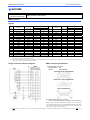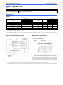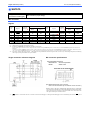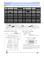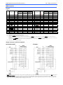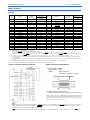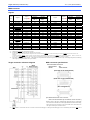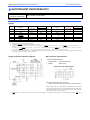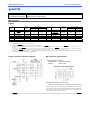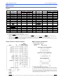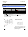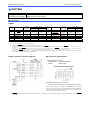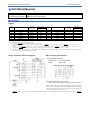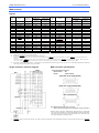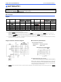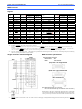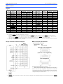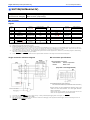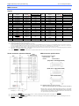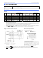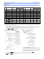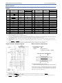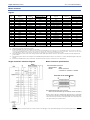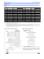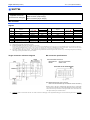
1
Technical Information
PALMiCE2 / PALMiCE3
SuperH-related Target Interface
Feb. 22, 2013
Tenth Edition
Go through the required procedures as stated under Foreign Exchange and Foreign Trade Control Law in exporting (including the case
where travellers directly carry) this product or providing this product for residents outside Japan.
No part of this manual, whether in whole or in part, may be adapted, copied or reproduced without prior permission.
The content of and the specifications of this product are subject to change without prior notice.
Computex Co., Ltd. shall not be held liable for any loss or damage arising from the use of this product although all possible measures
have been taken by Computex Co., Ltd. in good faith to ensure the quality of the product.
Contact us for any questions, feedback, comments, requests or anything of concern to you (or in the event of malfunction) regarding this
product or misprinting or missing information within this manual.
SuperH is a registered trademark or trademark of Renesas Electronics Corporation in Japan, the USA, and other countries.
Other names of CPUs etc. mentioned in this manual are trademarks or registered trademarks of their respective manufacturers.
COMPUTEX and PALMiCE are registered trademarks of Computex Co., Ltd. in Japan.
Copyright (C)2008 COMPUTEX Co., Ltd.
Document change history
First Edition
Second Edition
Feb. 12, 2008
Dec. 12, 2008
Third Edition
Jun. 30, 2009
Initial edition
Added a package to the table of Signals.
SH7750R
SH7751R
CSIDE for PALMiCE3-SH-E (Ver.5.10.00) was released.
・
Added PALMiCE3 to Applicable products for the following CPUs.
SH7047F
SH7083F/SH7084F/SH7085F/SH7086F
SH7144F/SH7145F
SH7606
SH7618
SH7615
SH7616
SH7206
SH7705
SH7706
SH7709S
SH7710
SH7712
SH7720
SH7727
SH7729
SH7729R
SH7750R/SH7750S
SH7751/SH7751R
SH7760
SH7780
・
Added the following CPUs to this manual.
SH7146F
SH7149F
SH7618A
SH7211F
SH7243F/SH7285F/ SH7286F
SH7201
SH7203
SH7261
SH7262/SH7264
SH7263
SH7670/SH7671/SH7672/SH7673
SH7205
SH7265
SH7290(SH-Mobile3AS)
SH7294(SH-MobileJ)
SH7300(SH-MobileV)
SH7713
SH7721
SH7343(SH-Mobile3AS)
SH7354(SH-MobileL3V)
SH7722(SH-MobileR)
SH7723(SH-MobileR2)
SH7730
SH7763
SH7764
SH7770
SH7774
SH7780
SH7781
SH7785
CSIDE for PALMiCE3 SH7055-E (Ver.5.07.00) was released.
・
Added the following CPUs to this manual.
SH7055F
SH7055SF
SH7058F
SH7058SF/SH7059F
Changed the descriptions of AUDSYNC signal regarding the following CPUs.
They had been written in negative logic, however, the descriptions were changed to positive logic
so that they conform to the descriptions in the hardware manual published by Renesas
Technology Corp..
SH7705
SH7751/SH7751R
SH7760
SH7780
Fourth Edition
Sep. 30, 2009
Fifth Edition
Jun. 1, 2010
Sixth Edition
Aug. 2, 2010
Seventh Edition
Apr. 01, 2011
Eighth Edition
Ninth Edition
Jul. 12, 2011
Apr. 11, 2012
Tenth Edition
Feb. 22, 2013
SH7243F/SH7285F/ SH7286F
Edited the note on MDR connector.
・ Made provision of support for Mictor connector.
SH7206
SH7211F
SH7243F/SH7285F/SH7286F
SH7201
SH7203
SH7261
SH7262/SH7264
SH7263
SH7205
SH7265
SH7723(SH-MobileR2)
SH7730
SH7764
・ SH7201, SH7261
Added the note on MDR connector.
・ SH7785
Edited the contents of note *3 and *4 of Mictor connector signal table.
・ SH7243F/SH7285F/SH7286F
The note on the use of PALMiCE3-SH AUD360 model given for MDR connector will now apply
to all connectors.
・ Added the note on the use of PALMiCE3-SH AUD360 model.
SH7083F/SH7084F/SH7085F/SH7086F
SH7146F
SH7149F
・ Added pages for description of the following:
PALMiCE3 - Supported connectors
PALMiCE3 - Target probe specifications
・ Changed the format.
・ Corrected the product name listed for Mictor probe under PALMiCE3 - Target probe
specifications as it contained errors.
[Correct] P3-SH-PRB-MIC38-MIC38 [Incorrect] P3-RE-PRB-MIC38-MIC38
・ PALMiCE3 - Supported connectors
Added the pin configuration and note.
PALMiCE3 - Supported connectors
(For detailed dimensions of the connectors, refer to the documentations by respective manufacturers of the connectors.)
36-pin MDR connector
●Top view on the target board
Recommended connector
Manufacturer : 3M
Model :
●Side view on the target board
10236-52A2JL
●Pin configuration
38-pin Mictor connector
●Top view on the target board and Pin configuration
Recommended connector
Manufacturer : AMP
Model :
Mictor connector
2-767004-2 / 767054-1 / 767061
14-pin MIL connector
●Top view on the target board and Pin configuration
Recommended connector
Manufacturer : Omron Corporation
Model :
XG4C-1431
* Please look at the pin configuration diagram and make sure that the connector is in the right
direction before connecting.
Moreover, please check the pin number in the corresponding signal table and make sure the signal and the pin
numbers match.
PALMiCE3 - Target probe specifications
Connector to be mounted
on the target board
Required target probe
36-pin MDR connector
AUD probe
38-pin Mictor connector
Mictor probe
14-pin MIL connector
HUDI cable
Target probe specifications
To be used by connecting it to PALMiCE3 main unit.
target system
Target probe
PALMiCE3
AUD probe
Product : P3-SH-PRB-MIC38-MDR36
Probe for connecting PALMiCE3 AUD360 main unit to
36-pin MDR connector on the target system.
(Unit: mm)
Mictor probe
Product : P3-SH-PRB-MIC38-MIC38
Probe for connecting PALMiCE3 AUD360 main unit to
38-pin Mictor connector on the target system.
(Unit: mm)
HUDI cable
Product : P3-CB-MIL14-MIL14
Probe for connecting PALMiCE3 HUDI141 main unit
to 14-pin MIL connector on the target system.
(Unit: mm)
SH-2
SH7047F
SH7055F
SH7055SF
SH7058F
SH7058SF/SH7059F
SH7083F/SH7084F/SH7085F/SH7086F
SH7144F/SH7145F
SH7146F
SH7149F
SH7606
SH7618/SH7618A
SH7619
Target interface (SH7047F)
Jun. 30, 2009 (Second Edition)
■ SH7047F
Applicable products
Applicable connectors
(Connectors for debugger)
PALMiCE3-SH / PALMiCE2-SH
MIL connector (14-pin design)
MDR connector (36-pin design)
MIL connector
Signals
Pin
No.
1
3
5
7
9
11
13
Signal
TCK
TRST
TDO
ASEBRKAK
TMS
TDI
RES
Input/
Output*1
Input
Input
Output
Output
Input
Input
Output
CPU Pin No.
QFP-100
63
58
60
11
59
61
87
Pin
No.
2
4
6
8
10
12
14
Signal
N.C.
GND(DBGMD)*2
GND
VCC *3
GND
GND
GND
Input/
Output*1
CPU Pin No.
QFP-100
(Input)
(16)
Output
・ For the pin where stated as N.C. in the table, leave the signal unconnected.
*1:
*2:
Input/output is based on the target system.
To debug, DBGMD pin needs to be brought to Low state.
*3:
For VCC, connect I/O power of CPU. Debugging can be performed even if the signal is N.C., however, by connecting I/O power, leak during
the target system power OFF can be prevented.
Shown in the target connection reference diagram is the circuit that brings DBGMD pin to Low state when you connect DBGMD signal to the connector for
debugger.
If you do not connect DBGMD signal to Pin No. 4 of the connector for debugger, the circuit that sets DBGMD pin by switch circuit will do. However, in such case,
do not connect DBGMD pin to Pin No. 4 of the connector for debugger, but connect Pin No. 4 of connector for the debugger to GND.
Target connection reference diagram
MIL connector specifications
Recommended connector
Manufacturer
Omron Corporation
Model
XG4C-1431
(Top view on the target board)
(For detailed dimensions of the connector,
refer to the documentation by manufacturer of the connector.)
*Please look at the pin configuration diagram above and make
sure that the connector is in the right direction before connecting.
Please check the pin number in the signal table above and make sure
the signal and the pin numbers match.
*1:
RES, which is connected to Pin No. 13 of the connector for debugger, is the signal that debugger uses for monitoring the state of RES pin of
CPU.
Target interface (SH7047F)
Jun. 30, 2009 (Second Edition)
MDR connector
Signals
Pin
No.
1
3
5
7
9
11
13
15
17
19
21
23
25
27
29
31
33
35
Signal
AUDCK
AUDATA0
AUDATA1
AUDATA2
AUDATA3
AUDSYNC
AUDRST
AUDMD
TCK
TMS
TRST
TDI
TDO
ASEBRKAK
VCC*3
RES
GND
N.C.
Input/
Output*1
Input/Output
Input/Output
Input/Output
Input/Output
Input/Output
Input/Output
Input
Input
Input
Input
Input
Input
Output
Output
Output
Output
CPU Pin No.
QFP-100
79
92
90
88
86
78
81
80
63
59
58
61
60
11
87
Pin
No.
2
4
6
8
10
12
14
16
18
20
22
24
26
28
30
32
34
36
Signal
GND
GND
GND
GND
GND
GND
GND
GND
GND
GND
GND(DBGMD)*2
GND
GND
GND
GND
GND
GND
GND
Input/
Output*1
CPU Pin No.
QFP-100
(Input)
(16)
・ For the pin where stated as N.C. in the table, leave the signal unconnected.
*1:
*2:
Input/output is based on the target system.
To debug, DBGMD pin needs to be brought to Low state.
*3:
For VCC, connect I/O power of CPU. Debugging can be performed even if the signal is N.C., however, by connecting I/O power, leak during
the target system power OFF can be prevented.
Shown in the target connection reference diagram is the circuit that brings DBGMD pin to Low state when you connect DBGMD signal to the connector for
debugger.
If you do not connect DBGMD signal to Pin No. 22 of the connector for debugger, the circuit that sets DBGMD pin by switch circuit will do. However, in such case,
do not connect DBGMD pin to Pin No. 22 of the connector for debugger, but connect Pin No. 22 of connector for the debugger to GND.
Target connection reference diagram
MDR connector specifications
Recommended connector
Manufacturer
3M
Model
10236-52A2JL
(Top view on the target board)
(Side view on the target board)
(Pin Configuration)
(For detailed dimensions of the connector,
refer to the documentation by manufacturer of the connector.)
*Please look at the pin configuration diagram above and make
sure that the connector is in the right direction before connecting.
Please check the pin number in the signal table above and make sure
the signal and the pin numbers match.
*1:
RES, which is connected to Pin No. 31 of the connector for debugger, is the signal that debugger uses for monitoring the state of RES pin of
CPU.
Target interface (SH7047F)
Jun. 30, 2009 (Second Edition)
Document change history (SH7047F)
First Edition
Second Edition
Feb. 12, 2008
Jun. 30, 2009
Initial edition
Added PALMiCE3-SH to Applicable products following the release of PALMiCE3-SH.
Target interface (SH7055F)
Jun. 30, 2009 (First Edition)
■ SH7055F
Applicable product
Applicable connector
(Connector for debugger)
PALMiCE3-SH7055
MDR connector (36-pin design)
MDR connector
Signals
Pin
No.
1
3
5
7
9
11
13
15
17
19
21
23
25
27
29
31
33
35
Signal
AUDCK
AUDATA0
AUDATA1
AUDATA2
AUDATA3
AUDSYNC
AUDRST
AUDMD
TCK
TMS
TRST
TDI
TDO
N.C.
VCC *2
RES
GND
N.C.
Input/
Output*1
Input/Output
Input/Output
Input/Output
Input/Output
Input/Output
Input/Output
Input
Input
Input
Input
Input
Input
Output
CPU Pin No.
FP-256H
245
241
242
243
244
246
238
240
236
232
233
234
235
Output
Output
58
Pin
No.
2
4
6
8
10
12
14
16
18
20
22
24
26
28
30
32
34
36
Signal
Input/
Output*1
CPU Pin No.
FP-256H
GND
GND
GND
GND
GND
GND
GND
GND
GND
GND
GND
GND
GND
GND
GND
GND
GND
GND
・ For the pin where stated as N.C. in the table, leave the signal unconnected.
*1:
*2:
Input/output is based on the target system.
For VCC, connect I/O power of CPU. Debugging can be performed even if the signal is N.C., however, by connecting I/O power, leak during
the target system power OFF can be prevented.
Target connection reference diagram
MDR connector specifications
Recommended connector
Manufacturer
3M
Model
10236-52A2JL
(Top view on the target board)
(Side view on the target board)
(Pin Configuration)
(For detailed dimensions of the connector,
refer to the documentation by manufacturer of the connector.)
*Please look at the pin configuration diagram above and make
sure that the connector is in the right direction before connecting.
Please check the pin number in the signal table above and make sure
the signal and the pin numbers match.
*1:
RES, which is connected to Pin No. 31 of the connector for debugger, is the signal that debugger uses for monitoring the state of RES pin of
CPU.
Target interface (SH7055F)
Jun. 30, 2009 (First Edition)
Document change history (SH7055F)
First Edition
Jun. 30, 2009
Initial edition
Target interface (SH7055SF)
Jun. 30, 2009 (First Edition)
■ SH7055SF
Applicable product
Applicable connector
(Connector for debugger)
PALMiCE3-SH7055
MDR connector (36-pin design)
MDR connector
Signals
Pin
No.
1
3
5
7
9
11
13
15
17
19
21
23
25
27
29
31
33
35
Signal
AUDCK
AUDATA0
AUDATA1
AUDATA2
AUDATA3
AUDSYNC
AUDRST
AUDMD
TCK
TMS
TRST
TDI
TDO
N.C.
VCC *2
RES
GND
N.C.
Input/
Output*1
Input/Output
Input/Output
Input/Output
Input/Output
Input/Output
Input/Output
Input
Input
Input
Input
Input
Input
Output
CPU Pin No.
FP-256H
245
241
242
243
244
246
238
240
236
232
233
234
235
Output
Output
58
Pin
No.
2
4
6
8
10
12
14
16
18
20
22
24
26
28
30
32
34
36
Signal
Input/
Output*1
CPU Pin No.
FP-256H
GND
GND
GND
GND
GND
GND
GND
GND
GND
GND
GND
GND
GND
GND
GND
GND
GND
GND
・ For the pin where stated as N.C. in the table, leave the signal unconnected.
*1:
*2:
Input/output is based on the target system.
For VCC, connect I/O power of CPU. Debugging can be performed even if the signal is N.C., however, by connecting I/O power, leak during
the target system power OFF can be prevented.
Target connection reference diagram
MDR connector specifications
Recommended connector
Manufacturer
3M
Model
10236-52A2JL
(Top view on the target board)
(Side view on the target board)
(Pin Configuration)
(For detailed dimensions of the connector,
refer to the documentation by manufacturer of the connector.)
*Please look at the pin configuration diagram above and make
sure that the connector is in the right direction before connecting.
Please check the pin number in the signal table above and make sure
the signal and the pin numbers match.
*1:
RES, which is connected to Pin No. 31 of the connector for debugger, is the signal that debugger uses for monitoring the state of RES pin of
CPU.
Target interface (SH7055SF)
Jun. 30, 2009 (First Edition)
Document change history (SH7055SF)
First Edition
Jun. 30, 2009
Initial edition
Target interface (SH7058F)
Jun. 30, 2009 (First Edition)
■ SH7058F
Applicable product
Applicable connector
(Connector for debugger)
PALMiCE3-SH7055
MDR connector (36-pin design)
MDR connector
Signals
Pin
No.
1
3
5
7
9
11
13
15
17
19
21
23
25
27
29
31
33
35
Signal
AUDCK
AUDATA0
AUDATA1
AUDATA2
AUDATA3
AUDSYNC
AUDRST
AUDMD
TCK
TMS
TRST
TDI
TDO
N.C.
VCC *2
RES
GND
N.C.
Input/
Output*1
Input/Output
Input/Output
Input/Output
Input/Output
Input/Output
Input/Output
Input
Input
Input
Input
Input
Input
Output
CPU Pin No.
FP-256H
BP-272
245
D1
241
G1
242
F1
243
G2
244
E1
246
F2
238
H2
240
H3
236
J2
232
K3
233
J1
234
K4
235
H1
Output
Output
58
Pin
No.
2
4
6
8
10
12
14
16
18
20
22
24
26
28
30
32
34
36
B16
Signal
Input/
Output*1
CPU Pin No.
FP-256H
BP-272
GND
GND
GND
GND
GND
GND
GND
GND
GND
GND
GND
GND
GND
GND
GND
GND
GND
GND
・ For the pin where stated as N.C. in the table, leave the signal unconnected.
*1:
*2:
Input/output is based on the target system.
For VCC, connect I/O power of CPU. Debugging can be performed even if the signal is N.C., however, by connecting I/O power, leak during
the target system power OFF can be prevented.
Target connection reference diagram
MDR connector specifications
Recommended connector
Manufacturer
3M
Model
10236-52A2JL
(Top view on the target board)
(Side view on the target board)
(Pin Configuration)
(For detailed dimensions of the connector,
refer to the documentation by manufacturer of the connector.)
*Please look at the pin configuration diagram above and make
sure that the connector is in the right direction before connecting.
Please check the pin number in the signal table above and make sure
the signal and the pin numbers match.
*1:
RES, which is connected to Pin No. 31 of the connector for debugger, is the signal that debugger uses for monitoring the state of RES pin of
CPU.
Target interface (SH7058F)
Jun. 30, 2009 (First Edition)
Document change history (SH7058F)
First Edition
Jun. 30, 2009
Initial edition
Target interface (SH7058SF/SH7059F)
Jun. 30, 2009 (First Edition)
■ SH7058SF/SH7059F
Applicable product
Applicable connector
(Connector for debugger)
PALMiCE3-SH7055
MDR connector (36-pin design)
MDR connector
Signals
Pin
No.
Signal
1
AUDCK
3
AUDATA0
5
AUDATA1
7
AUDATA2
9
AUDATA3
11
AUDSYNC
13
15
17
19
21
23
25
27
29
31
33
35
AUDRST
AUDMD
TCK
TMS
TRST
TDI
TDO
N.C.
VCC *2
RES
GND
N.C.
Input/
Output*1
Input/
Output
Input/
Output
Input/
Output
Input/
Output
Input/
Output
Input/
Output
Input
Input
Input
Input
Input
Input
Output
Output
Output
CPU Pin No.
FP-256H
BP-272
Pin
No.
Signal
245
D1
2
GND
241
G1
4
GND
242
F1
6
GND
243
G2
8
GND
244
E1
10
GND
246
F2
12
GND
238
240
236
232
233
234
235
H2
H3
J2
K3
J1
K4
H1
58
B16
14
16
18
20
22
24
26
28
30
32
34
36
GND
GND
GND
GND
GND
GND
GND
GND
GND
GND
GND
GND
Input/
Output*1
CPU Pin No.
FP-256H
BP-272
・ For the pin where stated as N.C. in the table, leave the signal unconnected.
*1:
*2:
Input/output is based on the target system.
For VCC, connect I/O power of CPU. Debugging can be performed even if the signal is N.C., however, by connecting I/O power, leak during
the target system power OFF can be prevented.
Target connection reference diagram
MDR connector specifications
Recommended connector
Manufacturer
3M
Model
10236-52A2JL
(Top view on the target board)
(Side view on the target board)
(Pin Configuration)
(For detailed dimensions of the connector,
refer to the documentation by manufacturer of the connector.)
*Please look at the pin configuration diagram above and make
sure that the connector is in the right direction before connecting.
Please check the pin number in the signal table above and make sure
the signal and the pin numbers match.
*1:
RES, which is connected to Pin No. 31 of the connector for debugger, is the signal that debugger uses for monitoring the state of RESpin of
CPU.
Target interface (SH7058SF/SH7059F)
Document change history (SH7058SF/SH7059F)
First Edition
Jun. 30, 2009
Initial edition
Jun. 30, 2009 (First Edition)
Target interface (SH7083F/SH7084F/SH7085F/SH7086F)
Aug. 2, 2010 (Third Edition)
■ SH7083F/SH7084F/SH7085F/SH7086F
Applicable products
Applicable connectors
(Connectors for debugger)
PALMiCE3-SH / PALMiCE2-SH
MIL connector (14-pin design)
MDR connector (36-pin design)
NB : When you use PALMiCE3-SH AUD360 model and if you are using CPU with voltage over 4.0V, please contact us.
MIL connector
Signals
Pin
No.
Signal
1
TCK
Input/
Output
*1
Input
7083F
TQFP
P-LBGA
-100
-112
80
A9
CPU Pin No.
7084F
7085F
LQFP
LQFP
-112
-144
89
143
7086F
LQFP
-176
Pin
No.
1
2
Input/
Output
Signal
*1
3
TRST
Input
77
A10
86
139
174
4
5
TDO
ASEBRKAK
/ ASEBRK
TMS
TDI
RES
Output
Input/
Output
Input
Input
Output
79
B9
88
142
176
6
100
A2
102
144
2
8
VCC *3
76
78
75
B10
D8
C9
85
87
84
138
140
108
172
175
132
10
12
14
GND
GND
GND
9
11
13
CPU Pin No.
7084F
7085F
LQFP
LQFP
-112
-144
7086F
LQFP
-176
N.C.
GND
(ASEMD0)*2
GND
7
7083F
TQFP
P-LBGA
-100
-112
(Input)
(27)
(L2)
(33)
(42)
(51)
Output
・ For the pin where stated as N.C. in the table, leave the signal unconnected.
*1:
*2:
*3:
Input/output is based on the target system.
ASEMD0To debug, ASEMD0 pin needs to be brought to Low state.
Shown in the target connection reference diagram is the circuit that brings ASEMD0 pin to Low state when you connect ASEMD0 signal to the connector for
debugger.
If you do not connect ASEMD0 signal to Pin No. 4 of the connector for debugger, the circuit that sets ASEMD0 pin by switch circuit will do. However, in such case,
do not connect ASEMD0 pin to Pin No. 4 of the connector for debugger, but connect Pin No. 4 of connector for the debugger to GND.
For VCC, connect I/O power of CPU. Debugging can be performed even if the signal is N.C., however, by connecting I/O power, leak during
the target system power OFF can be prevented.
Target connection reference diagram
MIL connector specifications
Recommended connector
Manufacturer
Omron Corporation
Model
XG4C-1431
(Top view on the target board)
(For detailed dimensions of the connector,
refer to the documentation by manufacturer of the connector.)
*Please look at the pin configuration diagram above and make
sure that the connector is in the right direction before connecting.
Please check the pin number in the signal table above and make sure
the signal and the pin numbers match.
*1:
RES, which is connected to Pin No. 13 of the connector for debugger, is the signal that debugger uses for monitoring the state of RES pin of
CPU.
Target interface (SH7083F/SH7084F/SH7085F/SH7086F)
Aug. 2, 2010 (Third Edition)
MDR connector
Signals
Pin
No.
Signal
1
3
5
7
9
11
13
15
17
19
AUDCK
AUDATA0
AUDATA1
AUDATA2
AUDATA3
AUDSYNC
N.C.
N.C.
TCK
TMS
21
TRST
23
25
TDI
TDO
ASEBRKAK
/ ASEBRK
VCC*4
RES
GND
N.C.
27
29
31
33
35
CPU Pin No.
Input/
Output
7083F
7084F
7085F
7086F
*2
*2
Pin
No.
Output
Output
Output
Output
Output
Output
TQFP
-100
45
51
50
49
48
44
P-LBGA
-112
H7
K10
L10
K9
J8
L8
LQFP
-112
53
60
59
58
57
52
LQFP
-144
65/109
72/116
70/115
69/114
68/113
64/100
LQFP
-176
89/133
97/140
95/139
93/138
92/137
88/124
Input
Input
80
76
A9
B10
89
85
143
138
1
172
2
4
6
8
10
12
14
16
18
20
Input
77
A10
86
139
174
22
Input
Output
Input/
Output
Output
Output
78
79
D8
B9
87
88
140
142
175
176
24
26
GND
GND
GND
GND
GND
GND
GND
GND
GND
GND
GND
(ASEMD0)*3
GND
GND
100
A2
102
144
2
28
GND
30
32
34
36
GND
GND
GND
GND
*1
75
C9
84
108
132
CPU Pin No.
Input/
Output
Signal
7084F
7085F
*2
*2
*1
TQFP
-100
P-LBGA
-112
LQFP
-112
LQFP
-144
LQFP
-176
(Input)
(27)
(L2)
(33)
(42)
(51)
7083F
7086F
・ For the pin where stated as N.C. in the table, leave the signal unconnected.
*1:
*2:
*3:
Input/output is based on the target system.
For SH7085F and SH7086F respectively, 2 routings of AUD ports are available.
To debug, ASEMD0 pin needs to be brought to Low state.
Choose either of the routings.
Shown in the target connection reference diagram is the circuit that brings ASEMD0 pin to Low state when you connect ASEMD0 signal to the connector for
debugger.
If you do not connect ASEMD0 signal to Pin No. 22 of the connector for debugger, the circuit that sets ASEMD0 pin by switch circuit will do. However, in such
case, do not connect ASEMD0 pin to Pin No. 22 of the connector for debugger, but connect Pin No. 22 of connector for the debugger to GND.
*4:
For VCC, connect I/O power of CPU. Debugging can be performed even if the signal is N.C., however, by connecting I/O power, leak during
the target system power OFF can be prevented.
Target connection reference diagram
MDR connector specifications
Recommended connector
Manufacturer
3M
Model
10236-52A2JL
(Top view on the target board)
(Side view on the target board)
(Pin Configuration)
(For detailed dimensions of the connector,
refer to the documentation by manufacturer of the connector.)
*Please look at the pin configuration diagram above and make
sure that the connector is in the right direction before connecting.
Please check the pin number in the signal table above and make sure
the signal and the pin numbers match.
*1:
RES, which is connected to Pin No. 31 of the connector for debugger, is the signal that debugger uses for monitoring the state of RES pin of
CPU.
Target interface (SH7083F/SH7084F/SH7085F/SH7086F)
Aug. 2, 2010 (Third Edition)
Document change history (SH7083F/SH7084F/SH7085F/SH7086F)
First Edition
Second Edition
Third Edition
Feb. 12, 2008
Jun. 30, 2009
Aug. 2, 2010
Initial edition
Added PALMiCE3-SH to Applicable products following the release of PALMiCE3-SH.
Added the note on the use of PALMiCE3-SH AUD360 model.
Target interface (SH7144F/SH7145F)
Jun. 30, 2009 (Second Edition)
■ SH7144F/SH7145F
Applicable products
Applicable connectors
(Connectors for debugger)
PALMiCE3-SH / PALMiCE2-SH
MIL connector (14-pin design)
MDR connector (36-pin design)
MIL connector
Signals
Pin
No.
Signal
Input/
Output*1
1
3
5
7
9
11
13
TCK
TRST
TDO
ASEBRKAK
TMS
TDI
RES
Input
Input
Output
Output
Input
Input
Output
CPU Pin No.
SH7144F
SH7145F
QFP-112
LQFP-144
89
143
86
139
88
142
27
35
85
138
87
140
84
108
Pin
No.
Signal
Input/
Output*1
2
4
6
8
10
12
14
N.C.
GND
GND
VCC *2
GND
GND
GND
Output
CPU Pin No.
SH7144F
SH7145F
QFP-112
LQFP-144
・ For the pin where stated as N.C. in the table, leave the signal unconnected.
*1:
*2:
Input/output is based on the target system.
For VCC, connect I/O power of CPU. Debugging can be performed even if the signal is N.C., however, by connecting I/O power, leak during
the target system power OFF can be prevented.
Target connection reference diagram
MIL connector specifications
Recommended connector
Manufacturer
Omron Corporation
Model
XG4C-1431
(Top view on the target board)
(For detailed dimensions of the connector,
refer to the documentation by manufacturer of the connector.)
*Please look at the pin configuration diagram above and make
sure that the connector is in the right direction before connecting.
Please check the pin number in the signal table above and make sure
the signal and the pin numbers match.
*1:
To debug, DBGMD pin needs to be brought to High state.
*2:
RES, which is connected to Pin No. 13 of the connector for debugger, is the signal that debugger uses for monitoring the state of RES pin of
CPU.
Shown in the target connection reference diagram is the circuit that brings DBGMD pin to High state when you turn OFF the switch.
Target interface (SH7144F/SH7145F)
Jun. 30, 2009 (Second Edition)
MDR connector
Signals
Pin
No.
Signal
1
3
5
7
9
11
13
15
17
19
21
23
25
27
29
31
33
35
AUDCK
AUDATA0
AUDATA1
AUDATA2
AUDATA3
AUDSYNC
AUDRST
AUDMD
TCK
TMS
TRST
TDI
TDO
ASEBRKAK
VCC*3
RES
GND
N.C.
Input/
Output*1
Input/Output
Input/Output
Input/Output
Input/Output
Input/Output
Input/Output
Input
Input
Input
Input
Input
Input
Output
Output
Output
Output
CPU Pin No.
SH7144F
SH7145F*2
QFP-112
LQFP-144
53
65/109
60
72/116
59
70/115
58
69/114
57
68/113
52
64/100
56
67/111
54
66/110
89
143
85
138
86
139
87
140
88
142
27
35
84
108
Pin
No.
Signal
2
4
6
8
10
12
14
16
18
20
22
24
26
28
30
32
34
36
GND
GND
GND
GND
GND
GND
GND
GND
GND
GND
GND
GND
GND
GND
GND
GND
GND
GND
Input/
Output*1
CPU Pin No.
SH7144F SH7145F*2
QFP-112
LQFP-144
・ For the pin where stated as N.C. in the table, leave the signal unconnected.
*1:
*2:
*3:
Input/output is based on the target system.
For SH7145F, 2 routings of AUD ports are available. Choose either of them.
For VCC, connect I/O power of CPU. Debugging can be performed even if the signal is N.C., however, by connecting I/O power, leak during
the target system power OFF can be prevented.
Target connection reference diagram
MDR connector specifications
Recommended connector
Manufacturer
3M
Model
10236-52A2JL
(Top view on the target board)
(Side view on the target board)
(Pin Configuration)
(For detailed dimensions of the connector,
refer to the documentation by manufacturer of the connector.)
*Please look at the pin configuration diagram above and make
sure that the connector is in the right direction before connecting.
Please check the pin number in the signal table above and make sure
the signal and the pin numbers match.
*1:
To debug, DBGMD pin needs to be brought to High state.
*2:
RES, which is connected to Pin No. 31 of the connector for debugger, is the signal that debugger uses for monitoring the state of RES pin of
CPU.
Shown in the target connection reference diagram is the circuit that brings DBGMD pin to High state when you turn OFF the switch.
Target interface (SH7144F/SH7145F)
Jun. 30, 2009 (Second Edition)
Document change history (SH7144F/SH7145F)
First Edition
Second Edition
Feb. 12, 2008
Jun. 30, 2009
Initial edition
Added PALMiCE3-SH to Applicable products following the release of PALMiCE3-SH.
Target interface (SH7146F)
Aug. 2, 2010 (Second Edition)
■ SH7146F
Applicable product
Applicable connector
(Connector for debugger)
PALMiCE3-SH
MIL connector (14-pin design)
NB : When you use PALMiCE3-SH AUD360 model and if you are using CPU with voltage over 4.0V, please contact us.
MIL connector
Signals
Pin
No.
1
3
5
7
9
11
13
Signal
TCK
TRST
TDO
ASEBRKAK
/ASEBRK
TMS
TDI
RES
Input/
Output*1
Input
Input
Output
Input/
Output
Input
Input
Output
CPU Pin No.
LQFP-80
7
1
3
Pin
No.
2
4
6
Signal
Input/
Output*1
CPU Pin No.
LQFP-80
N.C.
GND(ASEMD0)*2
GND
(Input)
(56)
8
8
VCC *3
Output
2
5
52
10
12
14
GND
GND
GND
・ For the pin where stated as N.C. in the table, leave the signal unconnected.
*1:
*2:
Input/output is based on the target system.
To debug, ASEMD0 pin needs to be brought to Low state.
Shown in the target connection reference diagram is the circuit that brings ASEMD0 pin to Low state when you connect ASEMD0 signal to the connector for
debugger.
If you do not connect ASEMD0 signal to Pin No. 4 of the connector for debugger, the circuit that sets ASEMD0 pin by switch circuit will do. However, in such case,
do not connect ASEMD0 pin to Pin No. 4 of the connector for debugger, but connect Pin No. 4 of connector for the debugger to GND.
*3:
For VCC, connect I/O power of CPU. Debugging can be performed even if the signal is N.C., however, by connecting I/O power, leak during
the target system power OFF can be prevented.
Target connection reference diagram
MIL connector specifications
Recommended connector
Manufacturer
Omron Corporation
Model
XG4C-1431
(Top view on the target board)
(For detailed dimensions of the connector,
refer to the documentation by manufacturer of the connector.)
*Please look at the pin configuration diagram above and make
sure that the connector is in the right direction before connecting.
Please check the pin number in the signal table above and make sure
the signal and the pin numbers match.
*1:
RES, which is connected to Pin No. 13 of the connector for debugger, is the signal that debugger uses for monitoring the state of RES pin of
CPU.
Target interface (SH7146F)
Aug. 2, 2010 (Second Edition)
Document change history (SH7146F)
First Edition
Second Edition
Jun. 30, 2009
Aug. 2, 2010
Initial edition
Added the note on the use of PALMiCE3-SH AUD360 model.
Target interface (SH7149F)
Aug. 2, 2010 (Second Edition)
■ SH7149F
Applicable product
Applicable connectors
(Connectors for debugger)
PALMiCE3-SH
MIL connector (14-pin design)
MDR connector (36-pin design)
NB : When you use PALMiCE3-SH AUD360 model and if you are using CPU with voltage over 4.0V, please contact us.
MIL connector
Signals
Pin
No.
1
3
5
7
9
11
13
Signal
TCK
TRST
TDO
ASEBRKAK
/ASEBRK
TMS
TDI
RES
Input/
Output*1
Input
Input
Output
Input/
Output
Input
Input
Output
CPU Pin No.
QFP-100
LQFP-100
6
3
2
99
4
1
Pin
No.
2
4
6
Signal
Input/
Output*1
N.C.
GND(ASEMD0)*2
GND
(Input)
Output
7
4
8
VCC *3
3
5
67
100
2
64
10
12
14
GND
GND
GND
CPU Pin No.
QFP-100
LQFP-100
(71)
(68)
・ For the pin where stated as N.C. in the table, leave the signal unconnected.
*1:
*2:
Input/output is based on the target system.
To debug, ASEMD0 pin needs to be brought to Low state.
*3:
For VCC, connect I/O power of CPU. Debugging can be performed even if the signal is N.C., however, by connecting I/O power, leak during
the target system power OFF can be prevented.
Shown in the target connection reference diagram is the circuit that brings ASEMD0 pin to Low state when you connect ASEMD0 signal to the connector for
debugger.
If you do not connect ASEMD0 signal to Pin No. 4 of the connector for debugger, the circuit that sets ASEMD0 pin by switch circuit will do. However, in such case,
do not connect ASEMD0 pin to Pin No. 4 of the connector for debugger, but connect Pin No. 4 of connector for the debugger to GND.
Target connection reference diagram
MIL connector specifications
Recommended connector
Manufacturer
Omron Corporation
Model
XG4C-1431
(Top view on the target board)
(For detailed dimensions of the connector,
refer to the documentation by manufacturer of the connector.)
*Please look at the pin configuration diagram above and make
sure that the connector is in the right direction before connecting.
Please check the pin number in the signal table above and make sure
the signal and the pin numbers match.
*1:
RES, which is connected to Pin No. 13 of the connector for debugger, is the signal that debugger uses for monitoring the state of RES pin of
CPU.
Target interface (SH7149F)
Aug. 2, 2010 (Second Edition)
MDR connector
Signals
Pin
No.
1
3
5
7
9
11
13
15
17
19
21
23
25
27
29
31
33
35
Signal
AUDCK
AUDATA0
AUDATA1
AUDATA2
AUDATA3
AUDSYNC
N.C.
N.C.
TCK
TMS
TRST
TDI
TDO
ASEBRKAK
/ASEBRK
VCC*3
RES
GND
N.C.
Input/
Output*1
Output
Output
Output
Output
Output
Output
CPU Pin No.
QFP-100
LQFP-100
31
28
37
34
36
33
35
32
34
31
30
27
Input
Input
Input
Input
Output
6
3
2
5
4
3
100
99
2
1
Pin
No.
2
4
6
8
10
12
14
16
18
20
22
24
26
Input/Output
7
4
28
GND
Output
Output
67
64
30
32
34
36
GND
GND
GND
GND
Input/
Output*1
Signal
GND
GND
GND
GND
GND
GND
GND
GND
GND
GND
GND(ASEMD0)*2
GND
GND
CPU Pin No.
QFP-100 LQFP-100
(Input)
(71)
(68)
・ For the pin where stated as N.C. in the table, leave the signal unconnected.
*1:
*2:
Input/output is based on the target system.
To debug, ASEMD0pin needs to be brought to Low state.
*3:
For VCC, connect I/O power of CPU. Debugging can be performed even if the signal is N.C., however, by connecting I/O power, leak during
the target system power OFF can be prevented.
Shown in the target connection reference diagram is the circuit that brings ASEMD0 pin to Low state when you connect ASEMD0 signal to the connector for
debugger.
If you do not connect ASEMD0 signal to Pin No. 22 of the connector for debugger, the circuit that sets ASEMD0 pin by switch circuit will do. However, in such
case, do not connect ASEMD0 pin to Pin No. 22 of the connector for debugger, but connect Pin No. 22 of connector for the debugger to GND.
Target connection reference diagram
MDR connector specifications
Recommended connector
Manufacturer
3M
Model
10236-52A2JL
(Top view on the target board)
(Side view on the target board)
(Pin Configuration)
(For detailed dimensions of the connector,
refer to the documentation by manufacturer of the connector.)
*Please look at the pin configuration diagram above and make
sure that the connector is in the right direction before connecting.
Please check the pin number in the signal table above and make sure
the signal and the pin numbers match.
*1:
RES, which is connected to Pin No. 31 of the connector for debugger, is the signal that debugger uses for monitoring the state of RES pin of
CPU.
Target interface (SH7149F)
Aug. 2, 2010 (Second Edition)
Document change history (SH7149F)
First Edition
Second Edition
Jun. 30, 2009
Aug. 2, 2010
Initial edition
Added the note on the use of PALMiCE3-SH AUD360 model.
Target interface (SH7606)
Jun. 30, 2009 (Second Edition)
■ SH7606
Applicable products
Applicable connector
(Connector for debugger)
PALMiCE3-SH / PALMiCE2-SH
MIL connector (14-pin design)
MIL connector
Signals
Pin
No.
1
3
5
7
9
11
13
Signal
TCK
TRST
TDO
N.C.
TMS
TDI
RES
Input/
Output*1
Input
Input
Output
CPU Pin No.
BP-176V
N10
M11
N11
Input
Input
Output
P11
R11
R12
Pin
No.
2
4
6
8
10
12
14
Signal
N.C.
GND(ASEMD)*2
GND
VCC *3
GND
GND
GND
Input/
Output*1
CPU Pin No.
BP-176V
(Input)
(N12)
Output
・ For the pin where stated as N.C. in the table, leave the signal unconnected.
*1:
*2:
Input/output is based on the target system.
To debug, ASEMD pin needs to be brought to Low state.
*3:
For VCC, connect I/O power of CPU. Debugging can be performed even if the signal is N.C., however, by connecting I/O power, leak during
the target system power OFF can be prevented.
Shown in the target connection reference diagram is the circuit that brings ASEMD pin to Low state when you connect ASEMD signal to the connector for
debugger.
If you do not connect ASEMD signal to Pin No. 4 of the connector for debugger, the circuit that sets ASEMD pin by switch circuit will do. However, in such case,
do not connect ASEMD pin to Pin No. 4 of the connector for debugger, but connect Pin No. 4 of connector for the debugger to GND.
Target connection reference diagram
MIL connector specifications
Recommended connector
Manufacturer
Omron Corporation
Model
XG4C-1431
(Top view on the target board)
(For detailed dimensions of the connector,
refer to the documentation by manufacturer of the connector.)
*Please look at the pin configuration diagram above and make
sure that the connector is in the right direction before connecting.
Please check the pin number in the signal table above and make sure
the signal and the pin numbers match.
*1:
RES, which is connected to Pin No. 13 of the connector for debugger, is the signal that debugger uses for monitoring the state of RES pin of
CPU.
Target interface (SH7606)
Jun. 30, 2009 (Second Edition)
Document change history (SH7606)
First Edition
Second Edition
Feb. 12, 2008
Jun. 30, 2009
Initial edition
Added PALMiCE3-SH to Applicable products following the release of PALMiCE3-SH.
Target interface (SH7618/SH7618A)
Jun. 30, 2009 (Second Edition)
■ SH7618/SH7618A
Applicable products*1
Applicable connector
(Connector for debugger)
PALMiCE3-SH / PALMiCE2-SH
MIL connector (14-pin design)
*1: SH7618A is not supported by PALMiCE2-SH.
MIL connector
Signals
Pin
No.
1
3
5
7
9
11
13
Signal
TCK
TRST
TDO
N.C.
TMS
TDI
RES
Input/
Output*1
Input
Input
Output
CPU Pin No.
PLBG0176GA-A
N10
M11
N11
Input
Input
Output
P11
R11
R12
Pin
No.
2
4
6
8
10
12
14
Signal
N.C.
GND(ASEMD)*2
GND
VCC *3
GND
GND
GND
Input/
Output*1
CPU Pin No.
PLBG0176GA-A
(Input)
(N12)
Output
・ For the pin where stated as N.C. in the table, leave the signal unconnected.
*1:
*2:
Input/output is based on the target system.
To debug, ASEMD pin needs to be brought to Low state.
Shown in the target connection reference diagram is the circuit that brings ASEMD pin to Low state when you connect ASEMD signal to the connector for
debugger.
If you do not connect ASEMD signal to Pin No. 4 of the connector for debugger, the circuit that sets ASEMD pin by switch circuit will do. However, in such case,
do not connect ASEMD pin to Pin No. 4 of the connector for debugger, but connect Pin No. 4 of connector for the debugger to GND.
*3:
For VCC, connect I/O power of CPU. Debugging can be performed even if the signal is N.C., however, by connecting I/O power, leak during
the target system power OFF can be prevented.
Target connection reference diagram
MIL connector specifications
Recommended connector
Manufacturer
Omron Corporation
Model
XG4C-1431
(Top view on the target board)
(For detailed dimensions of the connector,
refer to the documentation by manufacturer of the connector.)
*Please look at the pin configuration diagram above and make
sure that the connector is in the right direction before connecting.
Please check the pin number in the signal table above and make sure
the signal and the pin numbers match.
*1:
RES, which is connected to Pin No. 13 of the connector for debugger, is the signal that debugger uses for monitoring the state of RES pin of
CPU.
Target interface (SH7618/SH7618A)
Jun. 30, 2009 (Second Edition)
Document change history (SH7618/SH7618A)
First Edition
Second Edition
Feb. 12, 2008
Jun. 30, 2009
Initial edition
Added PALMiCE3-SH to Applicable products following its release.
Also, added CPU SH7618A.
Target interface (SH7619)
Jun. 30, 2009 (Second Edition)
■ SH7619
Applicable products
Applicable connector
(Connector for debugger)
PALMiCE3-SH / PALMiCE2-SH
MIL connector (14-pin design)
MIL connector
Signals
Pin
No.
1
3
5
7
9
11
13
Signal
TCK
TRST
TDO
N.C.
TMS
TDI
RES
Input/
Output*1
Input
Input
Output
CPU Pin No.
PLBG0176GA-A
P12
M14
N12
Input
Input
Output
M13
M12
M15
Pin
No.
2
4
6
8
10
12
14
Signal
N.C.
GND(ASEMD)*2
GND
VCC *3
GND
GND
GND
Input/
Output*1
CPU Pin No.
PLBG0176GA-A
(Input)
(L13)
Output
・ For the pin where stated as N.C. in the table, leave the signal unconnected.
*1:
*2:
Input/output is based on the target system.
To debug, ASEMD pin needs to be brought to Low state.
*3:
For VCC, connect I/O power of CPU. Debugging can be performed even if the signal is N.C., however, by connecting I/O power, leak during
the target system power OFF can be prevented.
Shown in the target connection reference diagram is the circuit that brings ASEMD pin to Low state when you connect ASEMD signal to the connector for
debugger.
If you do not connect ASEMD signal to Pin No. 4 of the connector for debugger, the circuit that sets ASEMD pin by switch circuit will do. However, in such case,
do not connect ASEMD pin to Pin No. 4 of the connector for debugger, but connect Pin No. 4 of connector for the debugger to GND.
Target connection reference diagram
MIL connector specifications
Recommended connector
Manufacturer
Omron Corporation
Model
XG4C-1431
(Top view on the target board)
(For detailed dimensions of the connector,
refer to the documentation by manufacturer of the connector.)
*Please look at the pin configuration diagram above and make
sure that the connector is in the right direction before connecting.
Please check the pin number in the signal table above and make sure
the signal and the pin numbers match.
*1:
RES, which is connected to Pin No. 13 of the connector for debugger, is the signal that debugger uses for monitoring the state of RES pin of
CPU.
Target interface (SH7619)
Jun. 30, 2009 (Second Edition)
Document change history (SH7619)
First Edition
Second Edition
Feb. 12, 2008
Jun. 30, 2009
Initial edition
Added PALMiCE3-SH to Applicable products following the release of PALMiCE3-SH.
SH2-DSP
SH7615
SH7616
Target interface (SH7615)
Jun. 30, 2009 (Second Edition)
■ SH7615
Applicable products
Applicable connector
(Connector for debugger)
PALMiCE3-SH / PALMiCE2-SH
MIL connector (14-pin design)
MIL connector
Signals
CPU Pin No.
PLQP0208
PLBG0240
KA-A
JA-A
30
L1
Pin
No.
Signal
Input/
Output*1
1
TCK
Input
3
TRST
Input
32
M3
4
5
7
9
11
13
TDO
N.C.
TMS
TDI
RES
Output
28
L4
Input
Input
Output
31
29
8
M4
L2
D3
6
8
10
12
14
Pin
No.
2
Signal
N.C.
GND
(ASEMODE)*2
GND
VCC *3
GND
GND
GND
Input/
Output*1
CPU Pin No.
PLQP0208
PLBG0240
KA-A
JA-A
(Input)
(6)
(E2)
Output
・ For the pin where stated as N.C. in the table, leave the signal unconnected.
*1:
*2:
Input/output is based on the target system.
To debug, ASEMODE pin needs to be brought to Low state.
*3:
For VCC, connect I/O power of CPU. Debugging can be performed even if the signal is N.C., however, by connecting I/O power, leak during
the target system power OFF can be prevented.
Shown in the target connection reference diagram is the circuit that brings ASEMODE pin to Low state when you connect ASEMODE signal to the connector for
debugger.
If you do not connect ASEMODE signal to Pin No. 4 of the connector for debugger, the circuit that sets ASEMODE pin by switch circuit will do. However, in such
case, do not connect ASEMODE pin to Pin No. 4 of the connector for debugger, but connect Pin No. 4 of connector for the debugger to GND.
Target connection reference diagram
MIL connector specifications
Recommended connector
Manufacturer
Omron Corporation
Model
XG4C-1431
(Top view on the target board)
(For detailed dimensions of the connector,
refer to the documentation by manufacturer of the connector.)
*Please look at the pin configuration diagram above and make
sure that the connector is in the right direction before connecting.
Please check the pin number in the signal table above and make sure
the signal and the pin numbers match.
*1:
RES, which is connected to Pin No. 13 of the connector for debugger, is the signal that debugger uses for monitoring the state of RES pin of
CPU.
Target interface (SH7615)
Jun. 30, 2009 (Second Edition)
Document change history (SH7615)
First Edition
Second Edition
Feb. 12, 2008
Jun. 30, 2009
Initial edition
Added PALMiCE3-SH to Applicable products following the release of PALMiCE3-SH.
Target interface (SH7616)
Jun. 30, 2009 (Second Edition)
■ SH7616
Applicable products
Applicable connector
(Connector for debugger)
PALMiCE3-SH / PALMiCE2-SH
MIL connector (14-pin design)
MIL connector
Signals
Pin
No.
1
3
5
7
9
11
13
Signal
TCK
TRST
TDO
N.C.
TMS
TDI
RES
Input/
Output*1
Input
Input
Output
CPU Pin No.
PLQP0208KA-A
30
32
28
Input
Input
Output
31
29
8
Pin
No.
2
4
6
8
10
12
14
Signal
N.C.
GND(ASEMODE)*2
GND
VCC *3
GND
GND
GND
Input/
Output*1
CPU Pin No.
PLQP0208KA-A
(Input)
(6)
Output
・ For the pin where stated as N.C. in the table, leave the signal unconnected.
*1:
*2:
Input/output is based on the target system.
To debug, ASEMODE pin needs to be brought to Low state.
*3:
For VCC, connect I/O power of CPU. Debugging can be performed even if the signal is N.C., however, by connecting I/O power, leak during
the target system power OFF can be prevented.
Shown in the target connection reference diagram is the circuit that brings ASEMODE pin to Low state when you connect ASEMODE signal to the connector for
debugger.
If you do not connect ASEMODE signal to Pin No. 4 of the connector for debugger, the circuit that sets ASEMODE pin by switch circuit will do. However, in such
case, do not connect ASEMODE pin to Pin No. 4 of the connector for debugger, but connect Pin No. 4 of connector for the debugger to GND.
Target connection reference diagram
MIL connector specifications
Recommended connector
Manufacturer
Omron Corporation
Model
XG4C-1431
(Top view on the target board)
(For detailed dimensions of the connector,
refer to the documentation by manufacturer of the connector.)
*Please look at the pin configuration diagram above and make
sure that the connector is in the right direction before connecting.
Please check the pin number in the signal table above and make sure
the signal and the pin numbers match.
*1:
RES, which is connected to Pin No. 13 of the connector for debugger, is the signal that debugger uses for monitoring the state of RES pin of
CPU.
Target interface (SH7616)
Jun. 30, 2009 (Second Edition)
Document change history (SH7616)
First Edition
Second Edition
Feb. 12, 2008
Jun. 30, 2009
Initial edition
Added PALMiCE3-SH to Applicable products following the release of PALMiCE3-SH.
SH-2A
SH7206
SH7211F
SH7243F/SH7285F/ SH7286F
Target interface (SH7206)
Jun. 1, 2010 (Third Edition)
■ SH7206
Applicable products
Applicable connectors
(Connectors for debugger)
PALMiCE3-SH / PALMiCE2-SH
MIL connector (14-pin design)
MDR connector (36-pin design)
Mictor connector (38-pin design)
MIL connector
Signals
Pin
No.
1
3
5
7
9
11
13
Signal
TCK
TRST
TDO
ASEBRKAK
/ASEBRK
TMS
TDI
RES
Input/
Output*1
Input
Input
Output
CPU Pin No.
LQFP-176
110
111
120
Pin
No.
2
4
6
Signal
Input/
Output*1
CPU Pin No.
LQFP-176
N.C.
GND(ASEMD)*2
GND
(Input)
(119)
Input/Output
104
8
VCC *3
Output
Input
Input
Output
116
112
37
10
12
14
GND
GND
GND
・ For the pin where stated as N.C. in the table, leave the signal unconnected.
*1:
*2:
Input/output is based on the target system.
To debug, ASEMD pin needs to be brought to Low state.
*3:
For VCC, connect I/O power of CPU. Debugging can be performed even if the signal is N.C., however, by connecting I/O power, leak during
the target system power OFF can be prevented.
Shown in the target connection reference diagram is the circuit that brings ASEMD pin to Low state when you connect ASEMD signal to the connector for
debugger.
If you do not connect ASEMD signal to Pin No. 4 of the connector for debugger, the circuit that sets ASEMD pin by switch circuit will do. However, in such case,
do not connect ASEMD pin to Pin No. 4 of the connector for debugger, but connect Pin No. 4 of connector for the debugger to GND.
Target connection reference diagram
MIL connector specifications
Recommended connector
Manufacturer
Omron Corporation
Model
XG4C-1431
(Top view on the target board)
(For detailed dimensions of the connector,
refer to the documentation by manufacturer of the connector.)
*Please look at the pin configuration diagram above and make
sure that the connector is in the right direction before connecting.
Please check the pin number in the signal table above and make sure
the signal and the pin numbers match.
*1:
RES, which is connected to Pin No. 13 of the connector for debugger, is the signal that debugger uses for monitoring the state of RES pin of
CPU.
Target interface (SH7206)
Jun. 1, 2010 (Third Edition)
MDR connector
Signals
Pin
No.
1
3
5
7
9
11
13
15
17
19
21
23
25
27
29
31
33
35
Signal
AUDCK
AUDATA0
AUDATA1
AUDATA2
AUDATA3
AUDSYNC
N.C.
N.C.
TCK
TMS
TRST
TDI
TDO
ASEBRKAK
/ASEBRK
VCC *4
RES
GND
N.C.
Input/
Output*1
Output
Output
Output
Output
Output
Output
CPU Pin No.*2
LQFP-176
75/134
84/140
82/139
86/138
80/137
132/167
Input
Input
Input
Input
Output
110
116
111
112
120
Pin
No.
2
4
6
8
10
12
14
16
18
20
22
24
26
GND
GND
GND
GND
GND
GND
GND
GND
GND
GND
GND(ASEMD)*3
GND
GND
Input/Output
104
28
GND
Output
Output
37
30
32
34
36
GND
GND
GND
GND
Signal
Input/
Output*1
CPU Pin No.*2
LQFP-176
(Input)
(119)
・ For the pin where stated as N.C. in the table, leave the signal unconnected.
*1:
*2:
*3:
Input/output is based on the target system.
2 routings of AUD ports are available. Choose either of them.
To debug, ASEMD pin needs to be brought to Low state.
*4:
For VCC, connect I/O power of CPU. Debugging can be performed even if the signal is N.C., however, by connecting I/O power, leak during
the target system power OFF can be prevented.
Shown in the target connection reference diagram is the circuit that brings ASEMD pin to Low state when you connect ASEMD signal to the connector for
debugger.
If you do not connect ASEMD signal to Pin No. 22 of the connector for debugger, the circuit that sets ASEMD pin by switch circuit will do. However, in such case,
do not connect ASEMD pin to Pin No. 22 of the connector for debugger, but connect Pin No. 22 of connector for the debugger to GND.
Target connection reference diagram
MDR connector specifications
Recommended connector
Manufacturer
3M
Model
10236-52A2JL
(Top view on the target board)
(Side view on the target board)
(Pin Configuration)
(For detailed dimensions of the connector,
refer to the documentation by manufacturer of the connector.)
*Please look at the pin configuration diagram above and make
sure that the connector is in the right direction before connecting.
Please check the pin number in the signal table above and make sure
the signal and the pin numbers match.
*1:
RES, which is connected to Pin No. 31 of the connector for debugger, is the signal that debugger uses for monitoring the state of RES pin of
CPU.
Target interface (SH7206)
Jun. 1, 2010 (Third Edition)
Mictor connector
Signals
Pin
No.
1
3
5
N.C.
GND (ASEMD) *3
GND (CON) *6
7
N.C.
9
11
13
15
17
19
21
23
25
27
29
31
33
35
37
RES
TDO
N.C.
TCK
TMS
TDI
TRST
N.C.
N.C.
N.C.
N.C.
N.C.
N.C.
N.C.
N.C.
Signal
Input/
Output*1
CPU Pin No.*2
LQFP-176
(Input)
(Output)
(119)
Output
Output
37
120
Input
Input
Input
Input
110
116
112
111
Pin
No.
2
4
6
8
10
12
14
16
18
20
22
24
26
28
30
32
34
36
38
Signal
N.C.
N.C.
AUDCK
ASEBRKAK
/ASEBRK
N.C.
VCC_AUD *4
VCC *5
N.C.
N.C.
N.C.
N.C.
AUDATA3
AUDATA2
AUDATA1
AUDATA0
AUDSYNC
N.C.
N.C.
N.C.
Input/
Output*1
CPU Pin No.*2
LQFP-176
Output
75/134
Input/Output
104
Output
Output
Output
Output
Output
Output
Output
80/137
86/138
82/139
84/140
132/167
・ For the pin where stated as N.C. in the table, leave the signal unconnected.
*1:
*2:
*3:
Input/output is based on the target system.
2 routings of AUD ports are available. Choose either of them.
To debug, ASEMD pin needs to be brought to Low state.
*4:
For VCC_AUD, the power same as the voltage level at which AUD signal of CPU works is to be connected. Connect the AUD signal to I/O
power of CPU.
For VCC, the power same as the voltage level at which HUDI signal of CPU works is to be connected. Connect the HUDI signal to I/O power
of CPU.
By detection of GND on the target system side, whether the target system is connected or not is determined.
*5:
*6:
Shown in the target connection reference diagram is the circuit that brings ASEMD pin to Low state when you connect ASEMD signal to the connector for
debugger. If you do not connect ASEMD signal to Pin No. 3 of the connector for debugger, the circuit that sets ASEMD pin by switch circuit will do. However, in
such case, do not connect ASEMD pin to Pin No. 3 of the connector for debugger, but connect Pin No. 3 of connector for the debugger to GND.
Target connection reference diagram
Mictor connector specifications
Recommended connector
Manufacturer
AMP
Model
Mictor connector
2-767004-2 / 767054-1 / 767061
(Top view on the target board)
(For detailed dimensions of the connector,
refer to the documentation by manufacturer of the connector.)
*Please look at the pin configuration diagram above and make
sure that the connector is in the right direction before connecting.
Please check the pin number in the signal table above and make sure
the signal and the pin numbers match.
*1:
RES, which is connected to Pin No. 9 of the connector for debugger, is the signal that debugger uses for monitoring the state of RES pin of
CPU.
Target interface (SH7206)
Jun. 1, 2010 (Third Edition)
Document change history (SH7206)
First Edition
Second Edition
Third Edition
Feb. 12, 2008
Jun. 30, 2009
Jun. 1, 2010
Initial edition
Added PALMiCE3-SH to Applicable products following the release of PALMiCE3-SH.
Made provision of support for Mictor connector.
Target interface (SH7211F)
Jun. 1, 2010 (Second Edition)
■ SH7211F
Applicable product
Applicable connectors
(Connectors for debugger)
PALMiCE3-SH
MIL connector (14-pin design)
MDR connector (36-pin design)
Mictor connector (38-pin design)
MIL connector
Signals
Pin
No.
1
3
5
7
9
11
13
Signal
TCK
TRST
TDO
ASEBRKAK
/ASEBRK
TMS
TDI
RES
Input/
Output*1
Input
Input
Output
CPU Pin No.
LQFP-144
16
18
15
Pin
No.
2
4
6
Signal
Input/
Output*1
CPU Pin No.
LQFP-144
N.C.
GND(ASEMD)*2
GND
(Input)
(29)
Input/Output
30
8
VCC *3
Output
Input
Input
Output
17
12
22
10
12
14
GND
GND
GND
・ For the pin where stated as N.C. in the table, leave the signal unconnected.
*1:
*2:
Input/output is based on the target system.
To debug, ASEMD pin needs to be brought to Low state.
*3:
For VCC, connect I/O power of CPU. Debugging can be performed even if the signal is N.C., however, by connecting I/O power, leak during
the target system power OFF can be prevented.
Shown in the target connection reference diagram is the circuit that brings ASEMD pin to Low state when you connect ASEMD signal to the connector for
debugger.
If you do not connect ASEMD signal to Pin No. 4 of the connector for debugger, the circuit that sets ASEMD pin by switch circuit will do. However, in such case,
do not connect ASEMD pin to Pin No. 4 of the connector for debugger, but connect Pin No. 4 of connector for the debugger to GND.
Target connection reference diagram
MIL connector specifications
Recommended connector
Manufacturer
Omron Corporation
Model
XG4C-1431
(Top view on the target board)
(For detailed dimensions of the connector,
refer to the documentation by manufacturer of the connector.)
*Please look at the pin configuration diagram above and make
sure that the connector is in the right direction before connecting.
Please check the pin number in the signal table above and make sure
the signal and the pin numbers match.
*1:
RES, which is connected to Pin No. 13 of the connector for debugger, is the signal that debugger uses for monitoring the state of RES pin of
CPU.
Target interface (SH7211F)
Jun. 1, 2010 (Second Edition)
MDR connector
Signals
Pin
No.
1
3
5
7
9
11
13
15
17
19
21
23
25
27
29
31
33
35
Signal
AUDCK
AUDATA0
AUDATA1
AUDATA2
AUDATA3
AUDSYNC
N.C.
N.C.
TCK
TMS
TRST
TDI
TDO
ASEBRKAK
/ASEBRK
VCC *3
RES
GND
N.C.
Input/
Output*1
Output
Output
Output
Output
Output
Output
CPU Pin No.
LQFP-144
110
116
115
112
111
109
Input
Input
Input
Input
Output
16
17
18
12
15
Pin
No.
2
4
6
8
10
12
14
16
18
20
22
24
26
GND
GND
GND
GND
GND
GND
GND
GND
GND
GND
GND(ASEMD)*2
GND
GND
Input/Output
30
28
GND
Output
Output
22
30
32
34
36
GND
GND
GND
GND
Signal
Input/
Output*1
CPU Pin No.
LQFP-144
(Input)
(29)
・ For the pin where stated as N.C. in the table, leave the signal unconnected.
*1:
*2:
Input/output is based on the target system.
To debug, ASEMD pin needs to be brought to Low state.
*3:
For VCC, connect I/O power of CPU. Debugging can be performed even if the signal is N.C., however, by connecting I/O power, leak during
the target system power OFF can be prevented.
Shown in the target connection reference diagram is the circuit that brings ASEMD pin to Low state when you connect ASEMD signal to the connector for
debugger.
If you do not connect ASEMD signal to Pin No. 22 of the connector for debugger, the circuit that sets ASEMD pin by switch circuit will do. However, in such case,
do not connect ASEMD pin to Pin No. 22 of the connector for debugger, but connect Pin No. 22 of connector for the debugger to GND.
Target connection reference diagram
MDR connector specifications
Recommended connector
Manufacturer
3M
Model
10236-52A2JL
(Top view on the target board)
(Side view on the target board)
(Pin Configuration)
(For detailed dimensions of the connector,
refer to the documentation by manufacturer of the connector.)
*Please look at the pin configuration diagram above and make
sure that the connector is in the right direction before connecting.
Please check the pin number in the signal table above and make sure
the signal and the pin numbers match.
*1:
RES, which is connected to Pin No. 31 of the connector for debugger, is the signal that debugger uses for monitoring the state of RES pin of
CPU.
Target interface (SH7211F)
Jun. 1, 2010 (Second Edition)
Mictor connector
Signals
Pin
No.
1
3
5
N.C.
GND (ASEMD) *2
GND (CON) *5
7
N.C.
9
11
13
15
17
19
21
23
25
27
29
31
33
35
37
RES
TDO
N.C.
TCK
TMS
TDI
TRST
N.C.
N.C.
N.C.
N.C.
N.C.
N.C.
N.C.
N.C.
Signal
Input/
Output*1
CPU Pin No.
LQFP-144
(Input)
(Output)
(29)
Output
Output
22
15
Input
Input
Input
Input
16
17
12
18
Pin
No.
2
4
6
8
10
12
14
16
18
20
22
24
26
28
30
32
34
36
38
Signal
N.C.
N.C.
AUDCK
ASEBRKAK
/ASEBRK
N.C.
VCC_AUD *3
VCC *4
N.C.
N.C.
N.C.
N.C.
AUDATA3
AUDATA2
AUDATA1
AUDATA0
AUDSYNC
N.C.
N.C.
N.C.
Input/
Output*1
CPU Pin No.
LQFP-144
Output
110
Input/Output
30
Output
Output
Output
Output
Output
Output
Output
111
112
115
116
109
・ For the pin where stated as N.C. in the table, leave the signal unconnected.
*1:
*2:
Input/output is based on the target system.
To debug, ASEMD pin needs to be brought to Low state.
*3:
For VCC_AUD, the power same as the voltage level at which AUD signal of CPU works is to be connected. Connect the AUD signal to I/O
power of CPU.
For VCC, the power same as the voltage level at which HUDI signal of CPU works is to be connected. Connect the HUDI signal to I/O power
of CPU.
By detection of GND on the target system side, whether the target system is connected or not is determined.
*4:
*5:
Shown in the target connection reference diagram is the circuit that brings ASEMD pin to Low state when you connect ASEMD signal to the connector for
debugger. If you do not connect ASEMD signal to Pin No. 3 of the connector for debugger, the circuit that sets ASEMD pin by switch circuit will do. However, in
such case, do not connect ASEMD pin to Pin No. 3 of the connector for debugger, but connect Pin No. 3 of connector for the debugger to GND.
Target connection reference diagram
Mictor connector specifications
Recommended connector
Manufacturer
AMP
Model
Mictor connector
2-767004-2 / 767054-1 / 767061
(Top view on the target board)
(For detailed dimensions of the connector,
refer to the documentation by manufacturer of the connector.)
*Please look at the pin configuration diagram above and make
sure that the connector is in the right direction before connecting.
Please check the pin number in the signal table above and make sure
the signal and the pin numbers match.
*1:
RES, which is connected to Pin No. 9 of the connector for debugger, is the signal that debugger uses for monitoring the state of RES pin of
CPU.
Target interface (SH7211F)
Jun. 1, 2010 (Second Edition)
Document change history (SH7211F)
First Edition
Second Edition
Jun. 30, 2009
Jun. 1, 2010
Initial edition
Made provision of support for Mictor connector.
Target interface (SH7243F/SH7285F/ SH7286F)
Aug. 2, 2010 (Fourth Edition)
■ SH7243F/SH7285F/ SH7286F
Applicable product
Applicable connectors
(Connectors for debugger)
PALMiCE3-SH
MIL connector (14-pin design)
MDR connector (36-pin design)
Mictor connector (38-pin design)
NB : When you use PALMiCE3-SH AUD360 model and if you are using CPU with voltage over 4.0V, please contact us.
MIL connector
Signals
Pin
No.
Signal
Input/
Output
*1
CPU Pin No.
SH7285F
SH7286F
LQFP-176
LQFP-100 LQFP-144
SH7243F
(FP-100UV)
(FP-144LV)
(FP-176AV,
FP-176EV)
Pin
No.
1
TCK
Input
8
133
91
2
3
TRST
Input
10
135
93
4
Signal
Input/
Output
*1
(Input)
5
N.C.
GND
(ASEMD0)*2
GND
7
VCC *3
Output
TDO
Output
7
132
90
6
Input/
ASEBRKAK/
77
114
134
8
ASEBRK
Output
9
TMS
Input
9
134
92
10
11
TDI
Input
6
131
89
12
13
RES
Output
76
113
133
14
・ For the pin where stated as N.C. in the table, leave the signal unconnected.
*1:
*2:
Input/output is based on the target system.
To debug, ASEMD0 pin needs to be brought to Low state.
*3:
For VCC, connect I/O power of CPU.
SH7243F
CPU Pin No.
SH7285F
LQFP-100
LQFP-144
(FP-100UV)
(FP-144LV)
(FP-176AV,
FP-176EV)
(78)
(115)
(135)
SH7286F
LQFP-176
GND
GND
GND
Shown in the target connection reference diagram is the circuit that brings ASEMD0 pin to Low state when you connect ASEMD0 signal to the connector for
debugger.
If you do not connect ASEMD0 signal to Pin No. 4 of the connector for debugger, the circuit that sets ASEMD0 pin by switch circuit will do. However, in such case,
do not connect ASEMD0 pin to Pin No. 4 of the connector for debugger, but connect Pin No. 4 of connector for the debugger to GND.
Target connection reference diagram
SH7243F/SH7285F
SH7286F
*1: RES, which is connected to Pin No. 13 of the connector for debugger, is the signal that debugger uses for monitoring the state of RES pin of CPU.
*2: ASEBRKAK/ASEBRK (Output/Input signals) are multiplexed with FWE (Input signal) in a pin. To allow the operation of the user target alone
when you use the ICE, in making signal arrangement, do not connect the pin to VCC nor GND directly, but connect it to a pull-up resistor with
ohmic value of 4.7K or a pull-down resistor with ohmic value of 100k.
MIL connector specifications
Recommended connector
Manufacturer Omron Corporation
Model
XG4C-1431
(Top view on the target board)
(For detailed dimensions of the connector, refer
to the documentation by manufacturer of the
connector.)
*Please look at the pin configuration diagram
above and make sure that the connector is in
the right direction before connecting.
Please check the pin number in the signal table
above and make sure the signal and the pin
numbers match.
Target interface (SH7243F/SH7285F/ SH7286F)
Aug. 2, 2010 (Fourth Edition)
MDR connector
Signals
Pin
No.
Signal
SH7243F
CPU Pin No.
SH7285F
*1
LQFP-100
LQFP-144
(FP-100UV)
(FP-144LV)
(FP-176AV,
FP-176EV)
Input/
Output
SH7286F
LQFP-176
Pin
No.
1
3
5
7
9
11
13
15
17
19
AUDCK
AUDATA0
AUDATA1
AUDATA2
AUDATA3
AUDSYNC
N.C.
N.C.
TCK
TMS
Output
Output
Output
Output
Output
Output
41
35
36
37
38
34
64
57
58
59
60
63
65
57
58
59
60
63
Input
Input
8
9
133
134
91
92
2
4
6
8
10
12
14
16
18
20
21
TRST
Input
10
135
93
22
23
25
TDI
Input
6
131
89
24
TDO
Output
7
132
90
26
ASEBRKAK Input/
77
114
134
28
27
/ASEBRK
Output
29
VCC *3
Output
30
31
RES
Output
76
113
133
32
33
GND
34
35
N.C.
36
・ For the pin where stated as N.C. in the table, leave the signal unconnected.
*1:
*2:
Input/output is based on the target system.
To debug, ASEMD0 pin needs to be brought to Low state.
*3:
For VCC, connect I/O power of CPU.
Signal
GND
GND
GND
GND
GND
GND
GND
GND
GND
GND
GND
(ASEMD0)*2
GND
GND
Input/
Outpu
t
SH7243F
CPU Pin No.
SH7285F
SH7286F
LQFP-176
*1
LQFP-100
LQFP-144
(FP-100UV)
(FP-144LV)
(FP-176AV,
FP-176EV)
(Input)
(78)
(115)
(135)
GND
GND
GND
GND
GND
Shown in the target connection reference diagram is the circuit that brings ASEMD0 pin to Low state when you connect ASEMD0 signal to the connector for
debugger.
If you do not connect ASEMD0 signal to Pin No. 4 of the connector for debugger, the circuit that sets ASEMD0 pin by switch circuit will do. However, in such case,
do not connect ASEMD0 pin to Pin No. 4 of the connector for debugger, but connect Pin No. 4 of connector for the debugger to GND.
Target connection reference diagram
SH7243F/SH7285F
SH7286F
*1: RES, which is connected to Pin No. 31 of the connector for debugger, is the signal that debugger uses for monitoring the state of RES pin of CPU.
*2:ASEBRKAK/ASEBRK (Output/Input signals) are multiplexed with FWE (Input signal) in a pin. To allow the operation of the user target alone
when you use the ICE, in making signal arrangement, do not connect the pin to VCC nor GND directly, but connect it to a pull-up resistor with
ohmic value of 4.7K or a pull-down resistor with ohmic value of 100k.
Target interface (SH7243F/SH7285F/ SH7286F)
Aug. 2, 2010 (Fourth Edition)
MDR connector specifications
Recommended connector
Manufacturer
3M
Model
10236-52A2JL
(Top view on the target board)
(Side view on the target board)
(Pin Configuration)
(For detailed dimensions of the connector, refer to the documentation by manufacturer of the connector.)
*Please look at the pin configuration diagram above and make sure that the connector is in the right direction before connecting.
Please check the pin number in the signal table above and make sure the signal and the pin numbers match.
Target interface (SH7243F/SH7285F/ SH7286F)
Aug. 2, 2010 (Fourth Edition)
Mictor connector
Signals
Pin
No.
1
3
5
7
Signal
Input/
Output
*1
N.C.
GND
(ASEMD0)*2
GND
(CON) *5
(Input)
SH7243F
CPU Pin No.
SH7285F
LQFP-100
LQFP-144
(FP-100UV)
(FP-144LV)
(78)
(115)
SH7286F
LQFP-176
(FP-176AV,
FP-176EV)
(135)
(Output)
N.C.
Pin
No.
SH7286F
LQFP-176
LQFP-100
LQFP-144
(FP-144LV)
(FP-176AV,
FP-176EV)
AUDCK
Output
41
64
65
ASEBRKAK
/ASEBRK
N.C.
VCC_AUD*3
VCC *4
N.C.
N.C.
N.C.
N.C.
AUDATA3
AUDATA2
AUDATA1
AUDATA0
AUDSYNC
N.C.
N.C.
N.C.
Input/
Output
77
114
134
38
37
36
35
34
60
59
58
57
63
60
59
58
57
63
4
N.C.
8
CPU Pin No.
SH7285F
(FP-100UV)
N.C.
6
SH7243F
*1
2
9
RES
Output
76
113
133
10
11
TDO
Output
7
132
90
12
13
N.C.
14
15
TCK
Input
8
133
91
16
17
TMS
Input
9
134
92
18
19
TDI
Input
6
131
89
20
21
TRST
Input
10
135
93
22
23
N.C.
24
25
N.C.
26
27
N.C.
28
29
N.C.
30
31
N.C.
32
33
N.C.
34
35
N.C.
36
37
N.C.
38
・ For the pin where stated as N.C. in the table, leave the signal unconnected.
*1:
*2:
Signal
Input/
Outpu
t
Output
Output
Output
Output
Output
Output
Output
Input/output is based on the target system.
To debug, ASEMD0 pin needs to be brought to Low state.
Shown in the target connection reference diagram is the circuit that brings ASEMD0 pin to Low state when you connect ASEMD0 signal to the connector for
debugger.
If you do not connect ASEMD0 signal to Pin No. 3 of the connector for debugger, the circuit that sets ASEMD0 pin by switch circuit will do. However, in such case,
do not connect ASEMD0 pin to Pin No. 3 of the connector for debugger, but connect Pin No. 3 of connector for the debugger to GND.
*3:
*4:
*5:
For VCC_AUD, the power same as the voltage level at which AUD signal of CPU works is to be connected. Connect the AUD signal to I/O
power of CPU.
For VCC, the power same as the voltage level at which HUDI signal of CPU works is to be connected. Connect the HUDI signal to I/O power
of CPU.
By detection of GND on the target system side, whether the target system is connected or not is determined.
Target connection reference diagram
SH7243F/SH7285F
SH7286F
*1: RES, which is connected to Pin No. 9 of the connector for debugger, is the signal that debugger uses for monitoring the state of RES pin of CPU.
*2:ASEBRKAK/ASEBRK (Output/Input signals) are multiplexed with FWE (Input signal) in a pin. To allow the operation of the user target alone
when you use the ICE, in making signal arrangement, do not connect the pin to VCC nor GND directly, but connect it to a pull-up resistor with
ohmic value of 4.7K or a pull-down resistor with ohmic value of 100k.
Target interface (SH7243F/SH7285F/ SH7286F)
Aug. 2, 2010 (Fourth Edition)
Mictor connector specifications
Recommended connector
Manufacturer
AMP
Model
Mictor connector
2-767004-2 / 767054-1 / 767061
(Top view on the target board)
(For detailed dimensions of the connector, refer to the documentation by manufacturer of the connector.)
*Please look at the pin configuration diagram above and make sure that the connector is in the right direction before connecting.
Please check the pin number in the signal table above and make sure the signal and the pin numbers match.
Target interface (SH7243F/SH7285F/ SH7286F)
Aug. 2, 2010 (Fourth Edition)
Document change history (SH7243F/SH7285F/ SH7286F)
First Edition
Second Edition
Third Edition
Fourth Edition
Jun. 30, 2009
Sep. 30, 2009
Jun. 1, 2010
Aug. 2. 2010
Initial edition
Edited the note on MDR connector.
Made provision of support for Mictor connector.
The note on the use of PALMiCE3-SH AUD360 model given for MDR connector will now apply
to all connectors.
SH2A-FPU
SH7201
SH7203
SH7261
SH7262/SH7264
SH7263
SH7670/SH7671/SH7672/SH7673
Target interface (SH7201)
Jun. 1, 2010 (Second Edition)
■ SH7201
Applicable product
Applicable connectors
(Connectors for debugger)
PALMiCE3-SH
MIL connector (14-pin design)
MDR connector (36-pin design)
Mictor connector (38-pin design)
MIL connector
Signals
Pin
No.
1
3
5
7
9
11
13
Signal
UDTCK
UDTRST
UDTDO
ASEBRKAK
/ASEBRK
UDTMS
UDTDI
RES
Input
Input
Output
CPU Pin No.
LQFP2424
-176Cu
131
126
129
Input/Output
132
8
VCC *3
Input
Input
Output
128
130
2
10
12
14
GND
GND
GND
Input/
Output*1
Pin
No.
Signal
Input/
Output*1
CPU Pin No.
LQFP2424
-176Cu
2
4
6
N.C.
GND(ASEMD)*2
GND
(Input)
(133)
Output
・ For the pin where stated as N.C. in the table, leave the signal unconnected.
*1:
*2:
Input/output is based on the target system.
To debug, ASEMD pin needs to be brought to Low state.
*3:
For VCC, connect I/O power of CPU. Debugging can be performed even if the signal is N.C., however, by connecting I/O power, leak during
the target system power OFF can be prevented.
Shown in the target connection reference diagram is the circuit that brings ASEMD pin to Low state when you connect ASEMD signal to the connector for
debugger.
If you do not connect ASEMD signal to Pin No. 4 of the connector for debugger, the circuit that sets ASEMD pin by switch circuit will do. However, in such case,
do not connect ASEMD pin to Pin No. 4 of the connector for debugger, but connect Pin No. 4 of connector for the debugger to GND.
Target connection reference diagram
MIL connector specifications
Recommended connector
Manufacturer
Omron Corporation
Model
XG4C-1431
(Top view on the target board)
(For detailed dimensions of the connector,
refer to the documentation by manufacturer of the connector.)
*Please look at the pin configuration diagram above and make
sure that the connector is in the right direction before connecting.
Please check the pin number in the signal table above and make sure
the signal and the pin numbers match.
*1:
RES, which is connected to Pin No. 13 of the connector for debugger, is the signal that debugger uses for monitoring the state of RES pin of
CPU.
Target interface (SH7201)
Jun. 1, 2010 (Second Edition)
MDR connector
Signals
Pin
No.
1
3
5
7
9
11
13
15
17
19
21
23
25
27
29
31
33
35
Signal
AUDCK
AUDATA0
AUDATA1
AUDATA2
AUDATA3
AUDSYNC
N.C.
N.C.
UDTCK
UDTMS
UDTRST
UDTDI
UDTDO
ASEBRKAK
/ASEBRK
VCC *3
RES
GND
N.C.
Output*4
Output*4
Output*4
Output*4
Output*4
Output*4
CPU Pin No.
LQFP2424
-176Cu
97
99
100
102
104
98
Input
Input
Input
Input
Output
131
128
126
130
129
2
4
6
8
10
12
14
16
18
20
22
24
26
Input/Output
132
28
GND
Output
Output
2
30
32
34
36
GND
GND
GND
GND
Input/
Output*1
Pin
No.
Signal
GND
GND
GND
GND
GND
GND
GND
GND
GND
GND
GND(ASEMD)*2
GND
GND
Input/
Output*1
CPU Pin No.
LQFP2424
-176Cu
(Input)
(133)
・ For the pin where stated as N.C. in the table, leave the signal unconnected.
*1:
*2:
Input/output is based on the target system.
To debug, ASEMD pin needs to be brought to Low state.
*3:
For VCC, connect I/O power of CPU. Debugging can be performed even if the signal is N.C., however, by connecting I/O power, leak during
the target system power OFF can be prevented.
It is used as an output signal as PALMiCE does not support RAM monitor function.
*4:
Shown in the target connection reference diagram is the circuit that brings ASEMD pin to Low state when you connect ASEMD signal to the connector for
debugger.
If you do not connect ASEMD signal to Pin No. 22 of the connector for debugger, the circuit that sets ASEMD pin by switch circuit will do. However, in such case,
do not connect ASEMD pin to Pin No. 22 of the connector for debugger, but connect Pin No. 22 of connector for the debugger to GND.
Target connection reference diagram
MDR connector specifications
Recommended connector
Manufacturer
3M
Model
10236-52A2JL
(Top view on the target board)
(Side view on the target board)
(Pin Configuration)
(For detailed dimensions of the connector,
refer to the documentation by manufacturer of the connector.)
*Please look at the pin configuration diagram above and make
sure that the connector is in the right direction before connecting.
*:
*1:
Please check the pin number in the signal table above and make sure
the signal and the pin numbers match.
When using the pins multiplexed with AUDMD or AUDRST signal, do not enable AUDMD nor AUDRST signal in Pin Function Controller.
When the debugger is used, neither AUDMD nor AUDRST signal is to be used; set the CPU to AUD trace mode. If you enable AUDMD or
AUDRST signal, it will inevitably change the setting of AUD.
RES, which is connected to Pin No. 31 of the connector for debugger, is the signal that debugger uses for monitoring the state of RES pin of
CPU.
Target interface (SH7201)
Jun. 1, 2010 (Second Edition)
Mictor connector
Signals
Pin
No.
Signal
1
3
5
N.C.
GND (ASEMD) *2
GND (CON) *5
7
N.C.
9
11
13
15
17
19
21
23
25
27
29
31
33
35
37
RES
UDTDO
N.C.
UDTCK
UDTMS
UDTDI
UDTRST
N.C.
N.C.
N.C.
N.C.
N.C.
N.C.
N.C.
N.C.
Input/
Output*1
(Input)
(Output)
CPU Pin No.
LQFP2424
-176Cu
Pin
No.
(133)
2
4
6
8
Output
Output
2
129
Input
Input
Input
Input
131
128
130
126
10
12
14
16
18
20
22
24
26
28
30
32
34
36
38
Signal
N.C.
N.C.
AUDCK
ASEBRKAK
/ASEBRK
N.C.
VCC_AUD *3
VCC *4
N.C.
N.C.
N.C.
N.C.
AUDATA3
AUDATA2
AUDATA1
AUDATA0
AUDSYNC
N.C.
N.C.
N.C.
Input/
Output*1
CPU Pin No.
LQFP2424
-176Cu
Output *6
97
Input/Output
132
Output
Output
Output *6
Output *6
Output *6
Output *6
Output *6
104
102
100
99
98
・ For the pin where stated as N.C. in the table, leave the signal unconnected.
*1:
*2:
Input/output is based on the target system.
To debug, ASEMD pin needs to be brought to Low state.
*3:
For VCC_AUD, the power same as the voltage level at which AUD signal of CPU works is to be connected. Connect the AUD signal to I/O
power of CPU.
For VCC, the power same as the voltage level at which HUDI signal of CPU works is to be connected. Connect the HUDI signal to I/O power
of CPU.
By detection of GND on the target system side, whether the target system is connected or not is determined.
It is used as an output signal as PALMiCE does not support RAM monitor function.
*4:
*5:
*6:
Shown in the target connection reference diagram is the circuit that brings ASEMD pin to Low state when you connect ASEMD signal to the connector for
debugger. If you do not connect ASEMD signal to Pin No. 3 of the connector for debugger, the circuit that sets ASEMD pin by switch circuit will do. However, in
such case, do not connect ASEMD pin to Pin No. 3 of the connector for debugger, but connect Pin No. 3 of connector for the debugger to GND.
Target connection reference diagram
Mictor connector specifications
Recommended connector
Manufacturer
AMP
Model
Mictor connector
2-767004-2 / 767054-1 / 767061
(Top view on the target board)
(For detailed dimensions of the connector,
refer to the documentation by manufacturer of the connector.)
*Please look at the pin configuration diagram above and make
sure that the connector is in the right direction before connecting.
Please check the pin number in the signal table above and make sure
the signal and the pin numbers match.
*:
When using the pins multiplexed with AUDMD or AUDRST signal, do not enable AUDMD nor AUDRST signal in Pin Function Controller.
When the debugger is used, neither AUDMD nor AUDRST signal is to be used; set the CPU to AUD trace mode. If you enable AUDMD or
AUDRST signal, it will inevitably change the setting of AUD.
*1:
RES, which is connected to Pin No. 9 of the connector for debugger, is the signal that debugger uses for monitoring the state of RES pin of
CPU.
Target interface (SH7201)
Jun. 1, 2010 (Second Edition)
Document change history (SH7201)
First Edition
Second Edition
Jun. 30, 2009
Jun. 1, 2010
Initial edition
・
Made provision of support for Mictor connector.
・
MDR connector
Added the note *4 to signal table.
Added notes to Target connection reference diagram.
Target interface (SH7203)
Jun. 1, 2010 (Second Edition)
■ SH7203
Applicable product
Applicable connectors
(Connectors for debugger)
PALMiCE3-SH
MIL connector (14-pin design)
MDR connector (36-pin design)
Mictor connector (38-pin design)
MIL connector
Signals
Pin
No.
1
3
5
7
9
11
13
Signal
TCK
TRST
TDO
ASEBRKAK
/ASEBRK
TMS
TDI
RES
Input
Input
Output
CPU Pin No.
QFP3232
-240Cu
178
176
177
Input/Output
175
8
VCC *3
Input
Input
Output
172
174
59
10
12
14
GND
GND
GND
Input/
Output*1
Pin
No.
Signal
Input/
Output*1
CPU Pin No.
QFP3232
-240Cu
2
4
6
N.C.
GND(ASEMD)*2
GND
(Input)
(61)
Output
・ For the pin where stated as N.C. in the table, leave the signal unconnected.
*1:
*2:
Input/output is based on the target system.
To debug, ASEMD pin needs to be brought to Low state.
*3:
For VCC, connect I/O power of CPU. Debugging can be performed even if the signal is N.C., however, by connecting I/O power, leak during
the target system power OFF can be prevented.
Shown in the target connection reference diagram is the circuit that brings ASEMD pin to Low state when you connect ASEMD signal to the connector for
debugger.
If you do not connect ASEMD signal to Pin No. 4 of the connector for debugger, the circuit that sets ASEMD pin by switch circuit will do. However, in such case,
do not connect ASEMD pin to Pin No. 4 of the connector for debugger, but connect Pin No. 4 of connector for the debugger to GND.
Target connection reference diagram
MIL connector specifications
Recommended connector
Manufacturer
Omron Corporation
Model
XG4C-1431
(Top view on the target board)
(For detailed dimensions of the connector,
refer to the documentation by manufacturer of the connector.)
*Please look at the pin configuration diagram above and make
sure that the connector is in the right direction before connecting.
Please check the pin number in the signal table above and make sure
the signal and the pin numbers match.
*1:
RES, which is connected to Pin No. 13 of the connector for debugger, is the signal that debugger uses for monitoring the state of RES pin of
CPU.
Target interface (SH7203)
Jun. 1, 2010 (Second Edition)
MDR connector
Signals
Pin
No.
1
3
5
7
9
11
13
15
17
19
21
23
25
27
29
31
33
35
Signal
AUDCK
AUDATA0
AUDATA1
AUDATA2
AUDATA3
AUDSYNC
N.C.
N.C.
TCK
TMS
TRST
TDI
TDO
ASEBRKAK
/ASEBRK
VCC *3
RES
GND
N.C.
Output
Output
Output
Output
Output
Output
CPU Pin No.
QFP3232
-240Cu
122
1
240
142
145
17
Input
Input
Input
Input
Output
178
172
176
174
177
2
4
6
8
10
12
14
16
18
20
22
24
26
Input/Output
175
28
GND
Output
Output
59
30
32
34
36
GND
GND
GND
GND
Input/
Output*1
Pin
No.
Signal
GND
GND
GND
GND
GND
GND
GND
GND
GND
GND
GND(ASEMD)*2
GND
GND
Input/
Output*1
CPU Pin No.
QFP3232
-240Cu
(Input)
(61)
・ For the pin where stated as N.C. in the table, leave the signal unconnected.
*1:
*2:
Input/output is based on the target system.
To debug, ASEMD pin needs to be brought to Low state.
*3:
For VCC, connect I/O power of CPU. Debugging can be performed even if the signal is N.C., however, by connecting I/O power, leak during
the target system power OFF can be prevented.
Shown in the target connection reference diagram is the circuit that brings ASEMD pin to Low state when you connect ASEMD signal to the connector for
debugger.
If you do not connect ASEMD signal to Pin No. 22 of the connector for debugger, the circuit that sets ASEMD pin by switch circuit will do. However, in such case,
do not connect ASEMD pin to Pin No. 22 of the connector for debugger, but connect Pin No. 22 of connector for the debugger to GND.
Target connection reference diagram
MDR connector specifications
Recommended connector
Manufacturer
3M
Model
10236-52A2JL
(Top view on the target board)
(Side view on the target board)
(Pin Configuration)
(For detailed dimensions of the connector,
refer to the documentation by manufacturer of the connector.)
*Please look at the pin configuration diagram above and make
sure that the connector is in the right direction before connecting.
Please check the pin number in the signal table above and make sure
the signal and the pin numbers match.
*1:
RES, which is connected to Pin No. 31 of the connector for debugger, is the signal that debugger uses for monitoring the state of RES pin of
CPU.
Target interface (SH7203)
Jun. 1, 2010 (Second Edition)
Mictor connector
Signals
Pin
No.
Signal
1
3
5
N.C.
GND (ASEMD) *2
GND (CON) *5
7
N.C.
9
11
13
15
17
19
21
23
25
27
29
31
33
35
37
RES
TDO
N.C.
TCK
TMS
TDI
TRST
N.C.
N.C.
N.C.
N.C.
N.C.
N.C.
N.C.
N.C.
Input/
Output*1
(Input)
(Output)
CPU Pin No.
QFP3232
-240Cu
Pin
No.
(61)
2
4
6
8
Output
Output
59
177
Input
Input
Input
Input
178
172
174
176
10
12
14
16
18
20
22
24
26
28
30
32
34
36
38
Signal
N.C.
N.C.
AUDCK
ASEBRKAK
/ASEBRK
N.C.
VCC_AUD *3
VCC *4
N.C.
N.C.
N.C.
N.C.
AUDATA3
AUDATA2
AUDATA1
AUDATA0
AUDSYNC
N.C.
N.C.
N.C.
Input/
Output*1
CPU Pin No.
QFP3232
-240Cu
Output
122
Input/Output
175
Output
Output
Output
Output
Output
Output
Output
145
142
240
1
17
・ For the pin where stated as N.C. in the table, leave the signal unconnected.
*1:
*2:
Input/output is based on the target system.
To debug, ASEMD pin needs to be brought to Low state.
*3:
For VCC_AUD, the power same as the voltage level at which AUD signal of CPU works is to be connected. Connect the AUD signal to I/O
power of CPU.
For VCC, the power same as the voltage level at which HUDI signal of CPU works is to be connected. Connect the HUDI signal to I/O power
of CPU.
By detection of GND on the target system side, whether the target system is connected or not is determined.
*4:
*5:
Shown in the target connection reference diagram is the circuit that brings ASEMD pin to Low state when you connect ASEMD signal to the connector for
debugger. If you do not connect ASEMD signal to Pin No. 3 of the connector for debugger, the circuit that sets ASEMD pin by switch circuit will do. However, in
such case, do not connect ASEMD pin to Pin No. 3 of the connector for debugger, but connect Pin No. 3 of connector for the debugger to GND.
Target connection reference diagram
Mictor connector specifications
Recommended connector
Manufacturer
AMP
Model
Mictor connector
2-767004-2 / 767054-1 / 767061
(Top view on the target board)
(For detailed dimensions of the connector,
refer to the documentation by manufacturer of the connector.)
*Please look at the pin configuration diagram above and make
sure that the connector is in the right direction before connecting.
Please check the pin number in the signal table above and make sure
the signal and the pin numbers match.
*1:
RES, which is connected to Pin No. 9 of the connector for debugger, is the signal that debugger uses for monitoring the state of RES pin of
CPU.
Target interface (SH7203)
Jun. 1, 2010 (Second Edition)
Document change history (SH7203)
First Edition
Second Edition
Jun. 30, 2009
Jun. 1, 2010
Initial edition
Made provision of support for Mictor connector.
Target interface (SH7261)
Jun. 1, 2010 (Second Edition)
■ SH7261
Applicable product
Applicable connectors
(Connectors for debugger)
PALMiCE3-SH
MIL connector (14-pin design)
MDR connector (36-pin design)
Mictor connector (38-pin design)
MIL connector
Signals
Pin
No.
1
3
5
7
9
11
13
Signal
UDTCK
UDTRST
UDTDO
ASEBRKAK
/ASEBRK
UDTMS
UDTDI
RES
Input
Input
Output
CPU Pin No.
LQFP2424
-176Cu
131
126
129
Input/Output
132
8
VCC *3
Input
Input
Output
128
130
2
10
12
14
GND
GND
GND
Input/
Output*1
Pin
No.
Signal
Input/
Output*1
CPU Pin No.
LQFP2424
-176Cu
2
4
6
N.C.
GND(ASEMD)*2
GND
(Input)
(133)
Output
・ For the pin where stated as N.C. in the table, leave the signal unconnected.
*1:
*2:
Input/output is based on the target system.
To debug, ASEMD pin needs to be brought to Low state.
*3:
For VCC, connect I/O power of CPU. Debugging can be performed even if the signal is N.C., however, by connecting I/O power, leak during
the target system power OFF can be prevented.
Shown in the target connection reference diagram is the circuit that brings ASEMD pin to Low state when you connect ASEMD signal to the connector for
debugger.
If you do not connect ASEMD signal to Pin No. 4 of the connector for debugger, the circuit that sets ASEMD pin by switch circuit will do. However, in such case,
do not connect ASEMD pin to Pin No. 4 of the connector for debugger, but connect Pin No. 4 of connector for the debugger to GND.
Target connection reference diagram
MIL connector specifications
Recommended connector
Manufacturer
Omron Corporation
Model
XG4C-1431
(Top view on the target board)
(For detailed dimensions of the connector,
refer to the documentation by manufacturer of the connector.)
*Please look at the pin configuration diagram above and make
sure that the connector is in the right direction before connecting.
Please check the pin number in the signal table above and make sure
the signal and the pin numbers match.
*1:
RES, which is connected to Pin No. 13 of the connector for debugger, is the signal that debugger uses for monitoring the state of RES pin of
CPU.
Target interface (SH7261)
Jun. 1, 2010 (Second Edition)
MDR connector
Signals
Pin
No.
1
3
5
7
9
11
13
15
17
19
21
23
25
27
29
31
33
35
Signal
AUDCK
AUDATA0
AUDATA1
AUDATA2
AUDATA3
AUDSYNC
N.C.
N.C.
UDTCK
UDTMS
UDTRST
UDTDI
UDTDO
ASEBRKAK
/ASEBRK
VCC *3
RES
GND
N.C.
Output*4
Output*4
Output*4
Output*4
Output*4
Output*4
CPU Pin No.
LQFP2424
-176Cu
97
99
100
102
104
98
Input
Input
Input
Input
Output
131
128
126
130
129
2
4
6
8
10
12
14
16
18
20
22
24
26
Input/Output
132
28
GND
Output
Output
2
30
32
34
36
GND
GND
GND
GND
Input/
Output*1
Pin
No.
Signal
GND
GND
GND
GND
GND
GND
GND
GND
GND
GND
GND(ASEMD)*2
GND
GND
Input/
Output*1
CPU Pin No.
LQFP2424
-176Cu
(Input)
(133)
・ For the pin where stated as N.C. in the table, leave the signal unconnected.
*1:
*2:
Input/output is based on the target system.
To debug, ASEMD pin needs to be brought to Low state.
*3:
For VCC, connect I/O power of CPU. Debugging can be performed even if the signal is N.C., however, by connecting I/O power, leak during
the target system power OFF can be prevented.
It is used as an output signal as PALMiCE does not support RAM monitor function.
*4:
Shown in the target connection reference diagram is the circuit that brings ASEMD pin to Low state when you connect ASEMD signal to the connector for
debugger.
If you do not connect ASEMD signal to Pin No. 22 of the connector for debugger, the circuit that sets ASEMD pin by switch circuit will do. However, in such case,
do not connect ASEMD pin to Pin No. 22 of the connector for debugger, but connect Pin No. 22 of connector for the debugger to GND.
Target connection reference diagram
MDR connector specifications
Recommended connector
Manufacturer
3M
Model
10236-52A2JL
(Top view on the target board)
(Side view on the target board)
(Pin Configuration)
(For detailed dimensions of the connector,
refer to the documentation by manufacturer of the connector.)
*Please look at the pin configuration diagram above and make
sure that the connector is in the right direction before connecting.
*:
*1:
Please check the pin number in the signal table above and make sure
the signal and the pin numbers match.
When using the pins multiplexed with AUDMD or AUDRST signal, do not enable AUDMD nor AUDRST signal in Pin Function Controller.
When the debugger is used, neither AUDMD nor AUDRST signal is to be used; set the CPU to AUD trace mode. If you enable AUDMD or
AUDRST signal, it will inevitably change the setting of AUD.
RES, which is connected to Pin No. 31 of the connector for debugger, is the signal that debugger uses for monitoring the state of RES pin of
CPU.
Target interface (SH7261)
Jun. 1, 2010 (Second Edition)
Mictor connector
Signals
Pin
No.
Signal
1
3
5
N.C.
GND (ASEMD) *2
GND (CON) *5
7
N.C.
9
11
13
15
17
19
21
23
25
27
29
31
33
35
37
RES
UDTDO
N.C.
UDTCK
UDTMS
UDTDI
UDTRST
N.C.
N.C.
N.C.
N.C.
N.C.
N.C.
N.C.
N.C.
Input/
Output*1
(Input)
(Output)
CPU Pin No.
LQFP2424
-176Cu
Pin
No.
(133)
2
4
6
8
Output
Output
2
129
Input
Input
Input
Input
131
128
130
126
10
12
14
16
18
20
22
24
26
28
30
32
34
36
38
Signal
N.C.
N.C.
AUDCK
ASEBRKAK
/ASEBRK
N.C.
VCC_AUD *3
VCC *4
N.C.
N.C.
N.C.
N.C.
AUDATA3
AUDATA2
AUDATA1
AUDATA0
AUDSYNC
N.C.
N.C.
N.C.
Input/
Output*1
CPU Pin No.
LQFP2424
-176Cu
Output*6
97
Input/Output
132
Output
Output
Output *6
Output *6
Output *6
Output *6
Output *6
104
102
100
99
98
・ For the pin where stated as N.C. in the table, leave the signal unconnected.
*1:
*2:
Input/output is based on the target system.
To debug, ASEMD pin needs to be brought to Low state.
Shown in the target connection reference diagram is the circuit that brings ASEMD pin to Low state when you connect ASEMD signal to the connector for
debugger.
If you do not connect ASEMD signal to Pin No. 3 of the connector for debugger, the circuit that sets ASEMD pin by switch circuit will do. However, in such case,
do not connect ASEMD pin to Pin No. 3 of the connector for debugger, but connect Pin No. 3 of connector for the debugger to GND.
*3:
*4:
*5:
*6:
For VCC_AUD, the power same as the voltage level at which AUD signal of CPU works is to be connected. Connect the AUD signal to I/O
power of CPU.
For VCC, the power same as the voltage level at which HUDI signal of CPU works is to be connected. Connect the HUDI signal to I/O power
of CPU.
By detection of GND on the target system side, whether the target system is connected or not is determined.
It is used as an output signal as PALMiCE does not support RAM monitor function.
Target connection reference diagram
Mictor connector specifications
Recommended connector
Manufacturer
AMP
Model
Mictor connector
2-767004-2 / 767054-1 / 767061
(Top view on the target board)
(For detailed dimensions of the connector,
refer to the documentation by manufacturer of the connector.)
*Please look at the pin configuration diagram above and make
sure that the connector is in the right direction before connecting.
Please check the pin number in the signal table above and make sure
the signal and the pin numbers match.
*:
When using the pins multiplexed with AUDMD or AUDRST signal, do not enable AUDMD nor AUDRST signal in Pin Function Controller.
When the debugger is used, neither AUDMD nor AUDRST signal is to be used; set the CPU to AUD trace mode. If you enable AUDMD or
AUDRST signal, it will inevitably change the setting of AUD.
*1:
RES, which is connected to Pin No. 9 of the connector for debugger, is the signal that debugger uses for monitoring the state of RES pin of
CPU.
Target interface (SH7261)
Jun. 1, 2010 (Second Edition)
Document change history (SH7261)
First Edition
Second Edition
Jun. 30, 2009
Jun. 1, 2010
Initial edition
・
Made provision of support for Mictor connector.
・
MDR connector
Added the note *4 to signal table.
Added notes to Target connection reference diagram.
Target interface (SH7262/SH7264)
Jun. 1, 2010 (Second Edition)
■ SH7262/SH7264
Applicable product
Applicable connectors
(Connectors for debugger)
PALMiCE3-SH
MIL connector (14-pin design)
MDR connector (36-pin design)
Mictor connector (38-pin design)
MIL connector
Signals
Pin
No.
1
3
5
7
9
11
13
Signal
TCK
TRST
TDO
ASEBRKAK
/ASEBRK
TMS
TDI
RES
Input/
Output*1
Input
Input
Output
CPU Pin No.
SH7262
SH7264
PLQP0176 PLQP0208
KB-A
KB-A
94
110
89
105
91
107
Pin
No.
Signal
Input/
Output*1
2
4
6
N.C.
GND(ASEMD)*2
GND
(Input)
Output
Input/Output
90
106
8
VCC *3
Input
Input
Output
93
92
43
109
108
51
10
12
14
GND
GND
GND
CPU Pin No.
SH7262
SH7264
PLQP0176 PLQP0208
KB-A
KB-A
(67)
(79)
・ For the pin where stated as N.C. in the table, leave the signal unconnected.
*1:
*2:
Input/output is based on the target system.
To debug, ASEMD pin needs to be brought to Low state.
Shown in the target connection reference diagram is the circuit that brings ASEMD pin to Low state when you connect ASEMD signal to the connector for
debugger.
If you do not connect ASEMD signal to Pin No. 4 of the connector for debugger, the circuit that sets ASEMD pin by switch circuit will do. However, in such case,
do not connect ASEMD pin to Pin No. 4 of the connector for debugger, but connect Pin No. 4 of connector for the debugger to GND.
*3:
For VCC, connect I/O power of CPU. Debugging can be performed even if the signal is N.C., however, by connecting I/O power, leak during
the target system power OFF can be prevented.
Target connection reference diagram
MIL connector specifications
Recommended connector
Manufacturer
Omron Corporation
Model
XG4C-1431
(Top view on the target board)
(For detailed dimensions of the connector,
refer to the documentation by manufacturer of the connector.)
*Please look at the pin configuration diagram above and make
sure that the connector is in the right direction before connecting.
Please check the pin number in the signal table above and make sure
the signal and the pin numbers match.
*1:
RES, which is connected to Pin No. 13 of the connector for debugger, is the signal that debugger uses for monitoring the state of RES pin of
CPU.
Target interface (SH7262/SH7264)
Jun. 1, 2010 (Second Edition)
MDR connector
Signals
Pin
No.
1
3
5
7
9
11
13
15
17
19
21
23
25
27
29
31
33
35
Signal
AUDCK
AUDATA0
AUDATA1
AUDATA2
AUDATA3
AUDSYNC
N.C.
N.C.
TCK
TMS
TRST
TDI
TDO
ASEBRKAK
/ASEBRK
VCC *3
RES
GND
N.C.
Input/
Output*1
Output
Output
Output
Output
Output
Output
CPU Pin No.
SH7262
SH7264
PLQP0176 PLQP0208
KB-A
KB-A
144
168
140
164
139
163
138
162
137
161
142
166
Pin
No.
Signal
GND
GND
GND
GND
GND
GND
GND
GND
GND
GND
GND(ASEMD)*2
GND
GND
Input
Input
Input
Input
Output
94
93
89
92
91
110
109
105
108
107
2
4
6
8
10
12
14
16
18
20
22
24
26
Input/Output
90
106
28
GND
Output
Output
43
51
30
32
34
36
GND
GND
GND
GND
Input/
Output*1
(Input)
CPU Pin No.
SH7262
SH7264
PLQP0176 PLQP0208
KB-A
KB-A
(67)
(79)
・ For the pin where stated as N.C. in the table, leave the signal unconnected.
*1:
*2:
Input/output is based on the target system.
To debug, ASEMD pin needs to be brought to Low state.
*3:
For VCC, connect I/O power of CPU. Debugging can be performed even if the signal is N.C., however, by connecting I/O power, leak during
the target system power OFF can be prevented.
Shown in the target connection reference diagram is the circuit that brings ASEMD pin to Low state when you connect ASEMD signal to the connector for
debugger.
If you do not connect ASEMD signal to Pin No. 22 of the connector for debugger, the circuit that sets ASEMD pin by switch circuit will do. However, in such case,
do not connect ASEMD pin to Pin No. 22 of the connector for debugger, but connect Pin No. 22 of connector for the debugger to GND.
Target connection reference diagram
MDR connector specifications
Recommended connector
Manufacturer
3M
Model
10236-52A2JL
(Top view on the target board)
(Side view on the target board)
(Pin Configuration)
(For detailed dimensions of the connector,
refer to the documentation by manufacturer of the connector.)
*Please look at the pin configuration diagram above and make
sure that the connector is in the right direction before connecting.
Please check the pin number in the signal table above and make sure
the signal and the pin numbers match.
*1:
RES, which is connected to Pin No. 31 of the connector for debugger, is the signal that debugger uses for monitoring the state of RES pin of
CPU.
Target interface (SH7262/SH7264)
Jun. 1, 2010 (Second Edition)
Mictor connector
Signals
Pin
No.
Signal
Input/
Output*1
(Input)
5
N.C.
GND
(ASEMD) *2
GND(CON) 5
7
N.C.
9
11
13
15
17
19
21
23
25
27
29
31
33
35
37
RES
TDO
N.C.
TCK
TMS
TDI
TRST
N.C.
N.C.
N.C.
N.C.
N.C.
N.C.
N.C.
N.C.
1
3
CPU Pin No.
SH7262
SH7264
PLQP0176 PLQP0208
KB-A
KB-A
(67)
(79)
(Output)
Pin
No.
Signal
2
N.C.
4
N.C.
6
AUDCK
ASEBRKAK
/ASEBRK
N.C.
VCC_AUD *3
VCC *4
N.C.
N.C.
N.C.
N.C.
AUDATA3
AUDATA2
AUDATA1
AUDATA0
AUDSYNC
N.C.
N.C.
N.C.
8
Output
Output
43
91
51
107
Input
Input
Input
Input
94
93
92
89
110
109
108
105
10
12
14
16
18
20
22
24
26
28
30
32
34
36
38
Input/
Output*1
CPU Pin No.
SH7262
SH7264
PLQP0176 PLQP0208
KB-A
KB-A
Output
144
168
Input/Output
90
106
137
138
139
140
142
161
162
163
164
166
Output
Output
Output
Output
Output
Output
Output
・ For the pin where stated as N.C. in the table, leave the signal unconnected.
*1:
*2:
Input/output is based on the target system.
To debug, ASEMD pin needs to be brought to Low state.
*3:
For VCC_AUD, the power same as the voltage level at which AUD signal of CPU works is to be connected. Connect the AUD signal to I/O
power of CPU.
For VCC, the power same as the voltage level at which HUDI signal of CPU works is to be connected. Connect the HUDI signal to I/O power
of CPU.
By detection of GND on the target system side, whether the target system is connected or not is determined.
*4:
*5:
Shown in the target connection reference diagram is the circuit that brings ASEMD pin to Low state when you connect ASEMD signal to the connector for
debugger.
If you do not connect ASEMD signal to Pin No. 3 of the connector for debugger, the circuit that sets ASEMD pin by switch circuit will do. However, in such case,
do not connect ASEMD pin to Pin No. 3 of the connector for debugger, but connect Pin No. 3 of connector for the debugger to GND.
Target connection reference diagram
Mictor connector specifications
Recommended connector
Manufacturer
AMP
Model
Mictor connector
2-767004-2 / 767054-1 / 767061
(Top view on the target board)
(For detailed dimensions of the connector,
refer to the documentation by manufacturer of the connector.)
*Please look at the pin configuration diagram above and make
sure that the connector is in the right direction before connecting.
Please check the pin number in the signal table above and make sure
the signal and the pin numbers match.
*1:
RES, which is connected to Pin No. 9 of the connector for debugger, is the signal that debugger uses for monitoring the state of RES pin of
CPU.
Target interface (SH7262/SH7264)
Jun. 1, 2010 (Second Edition)
Document change history (SH7262/SH7264)
First Edition
Second Edition
Jun. 30, 2009
Jun. 1, 2010
Initial edition
Made provision of support for Mictor connector.
Target interface (SH7263)
Jun. 1, 2010 (Second Edition)
■ SH7263
Applicable product
Applicable connectors
(Connectors for debugger)
PALMiCE3-SH
MIL connector (14-pin design)
MDR connector (36-pin design)
Mictor connector (38-pin design)
MIL connector
Signals
Pin
No.
1
3
5
7
9
11
13
Signal
TCK
TRST
TDO
ASEBRKAK
/ASEBRK
TMS
TDI
RES
Input
Input
Output
CPU Pin No.
QFP3232
-240Cu
178
176
177
Input/Output
175
8
VCC *3
Input
Input
Output
172
174
59
10
12
14
GND
GND
GND
Input/
Output*1
Pin
No.
Signal
Input/
Output*1
CPU Pin No.
QFP3232
-240Cu
2
4
6
N.C.
GND(ASEMD)*2
GND
(Input)
(61)
Output
・ For the pin where stated as N.C. in the table, leave the signal unconnected.
*1:
*2:
Input/output is based on the target system.
To debug, ASEMD pin needs to be brought to Low state.
*3:
For VCC, connect I/O power of CPU. Debugging can be performed even if the signal is N.C., however, by connecting I/O power, leak during
the target system power OFF can be prevented.
Shown in the target connection reference diagram is the circuit that brings ASEMD pin to Low state when you connect ASEMD signal to the connector for
debugger.
If you do not connect ASEMD signal to Pin No. 4 of the connector for debugger, the circuit that sets ASEMD pin by switch circuit will do. However, in such case,
do not connect ASEMD pin to Pin No. 4 of the connector for debugger, but connect Pin No. 4 of connector for the debugger to GND.
Target connection reference diagram
MIL connector specifications
Recommended connector
Manufacturer
Omron Corporation
Model
XG4C-1431
(Top view on the target board)
(For detailed dimensions of the connector,
refer to the documentation by manufacturer of the connector.)
*Please look at the pin configuration diagram above and make
sure that the connector is in the right direction before connecting.
Please check the pin number in the signal table above and make sure
the signal and the pin numbers match.
*1:
RES, which is connected to Pin No. 13 of the connector for debugger, is the signal that debugger uses for monitoring the state of RES pin of
CPU.
Target interface (SH7263)
Jun. 1, 2010 (Second Edition)
MDR connector
Signals
Pin
No.
1
3
5
7
9
11
13
15
17
19
21
23
25
27
29
31
33
35
Signal
AUDCK
AUDATA0
AUDATA1
AUDATA2
AUDATA3
AUDSYNC
N.C.
N.C.
TCK
TMS
TRST
TDI
TDO
ASEBRKAK
/ASEBRK
VCC *3
RES
GND
N.C.
Output
Output
Output
Output
Output
Output
CPU Pin No.
QFP3232
-240Cu
122
1
240
142
145
17
Input
Input
Input
Input
Output
178
172
176
174
177
2
4
6
8
10
12
14
16
18
20
22
24
26
Input/Output
175
28
GND
Output
Output
59
30
32
34
36
GND
GND
GND
GND
Input/
Output*1
Pin
No.
Signal
GND
GND
GND
GND
GND
GND
GND
GND
GND
GND
GND(ASEMD)*2
GND
GND
Input/
Output*1
CPU Pin No.
QFP3232
-240Cu
(Input)
(61)
・ For the pin where stated as N.C. in the table, leave the signal unconnected.
*1:
*2:
Input/output is based on the target system.
To debug, ASEMD pin needs to be brought to Low state.
*3:
For VCC, connect I/O power of CPU. Debugging can be performed even if the signal is N.C., however, by connecting I/O power, leak during
the target system power OFF can be prevented.
Shown in the target connection reference diagram is the circuit that brings ASEMD pin to Low state when you connect ASEMD signal to the connector for
debugger.
If you do not connect ASEMD signal to Pin No. 22 of the connector for debugger, the circuit that sets ASEMD pin by switch circuit will do. However, in such case,
do not connect ASEMD pin to Pin No. 22 of the connector for debugger, but connect Pin No. 22 of connector for the debugger to GND.
Target connection reference diagram
MDR connector specifications
Recommended connector
Manufacturer
3M
Model
10236-52A2JL
(Top view on the target board)
(Side view on the target board)
(Pin Configuration)
(For detailed dimensions of the connector,
refer to the documentation by manufacturer of the connector.)
*Please look at the pin configuration diagram above and make
sure that the connector is in the right direction before connecting.
Please check the pin number in the signal table above and make sure
the signal and the pin numbers match.
*1:
RES, which is connected to Pin No. 31 of the connector for debugger, is the signal that debugger uses for monitoring the state of RES pin of
CPU.
Target interface (SH7263)
Jun. 1, 2010 (Second Edition)
Mictor connector
Signals
Pin
No.
Signal
1
3
5
N.C.
GND (ASEMD) *2
GND (CON) *5
7
N.C.
9
11
13
15
17
19
21
23
25
27
29
31
33
35
37
RES
TDO
N.C.
TCK
TMS
TDI
TRST
N.C.
N.C.
N.C.
N.C.
N.C.
N.C.
N.C.
N.C.
Input/
Output*1
(Input)
(Output)
CPU Pin No.
QFP3232
-240Cu
Pin
No.
(61)
2
4
6
8
Output
Output
59
177
Input
Input
Input
Input
178
172
174
176
10
12
14
16
18
20
22
24
26
28
30
32
34
36
38
Signal
N.C.
N.C.
AUDCK
ASEBRKAK
/ASEBRK
N.C.
VCC_AUD *3
VCC *4
N.C.
N.C.
N.C.
N.C.
AUDATA3
AUDATA2
AUDATA1
AUDATA0
AUDSYNC
N.C.
N.C.
N.C.
Input/
Output*1
CPU Pin No.
QFP3232
-240Cu
Output
122
Input/Output
175
Output
Output
Output
Output
Output
Output
Output
145
142
240
1
17
・ For the pin where stated as N.C. in the table, leave the signal unconnected.
*1:
*2:
Input/output is based on the target system.
To debug, ASEMD pin needs to be brought to Low state.
*3:
For VCC_AUD, the power same as the voltage level at which AUD signal of CPU works is to be connected. Connect the AUD signal to I/O
power of CPU.
For VCC, the power same as the voltage level at which HUDI signal of CPU works is to be connected. Connect the HUDI signal to I/O power
of CPU.
By detection of GND on the target system side, whether the target system is connected or not is determined.
*4:
*5:
Shown in the target connection reference diagram is the circuit that brings ASEMD pin to Low state when you connect ASEMD signal to the connector for
debugger.
If you do not connect ASEMD signal to Pin No. 3 of the connector for debugger, the circuit that sets ASEMD pin by switch circuit will do. However, in such case,
do not connect ASEMD pin to Pin No. 3 of the connector for debugger, but connect Pin No. 3 of connector for the debugger to GND.
Target connection reference diagram
Mictor connector specifications
Recommended connector
Manufacturer
AMP
Model
Mictor connector
2-767004-2 / 767054-1 / 767061
(Top view on the target board)
(For detailed dimensions of the connector,
refer to the documentation by manufacturer of the connector.)
*Please look at the pin configuration diagram above and make
sure that the connector is in the right direction before connecting.
Please check the pin number in the signal table above and make sure
the signal and the pin numbers match.
*1:
RES, which is connected to Pin No. 9 of the connector for debugger, is the signal that debugger uses for monitoring the state of RES pin of
CPU.
Target interface (SH7263)
Jun. 1, 2010 (Second Edition)
Document change history (SH7263)
First Edition
Second Edition
Jun. 30, 2009
Jun. 1, 2010
Initial edition
Made provision of support for Mictor connector.
Target interface (SH7670/SH7671/SH7672/SH7673)
Jun. 30, 2009 (First Edition)
■ SH7670/SH7671/SH7672/SH7673
Applicable products
Applicable connector
(Connector for debugger)
PALMiCE3-SH
MIL connector (14-pin design)
MIL connector
Signals
Pin
No.
1
3
5
7
9
11
13
Signal
TCK
TRST
TDO
ASEBRKAK
/ASEBRK
TMS
TDI
RES
Input/
Output*1
Input
Input
Output
CPU Pin No.
P-FBGA256
V17
Y18
W19
Pin
No.
2
4
6
Signal
Input/
Output*1
CPU Pin No.
P-FBGA256
N.C.
GND(ASEMD)*2
GND
(Input)
(M2)
Input/Output
T20
8
VCC *3
Output
Input
Input
Output
Y19
V18
W18
10
12
14
GND
GND
GND
・ For the pin where stated as N.C. in the table, leave the signal unconnected.
*1:
*2:
Input/output is based on the target system.
To debug, ASEMD pin needs to be brought to Low state.
Shown in the target connection reference diagram is the circuit that brings ASEMD pin to Low state when you connect ASEMD signal to the connector for
debugger.
If you do not connect ASEMD signal to Pin No. 4 of the connector for debugger, the circuit that sets ASEMD pin by switch circuit will do. However, in such case,
do not connect ASEMD pin to Pin No. 4 of the connector for debugger, but connect Pin No. 4 of connector for the debugger to GND.
*3:
For VCC, connect I/O power of CPU. Debugging can be performed even if the signal is N.C., however, by connecting I/O power, leak during
the target system power OFF can be prevented.
Target connection reference diagram
MIL connector specifications
Recommended connector
Manufacturer
Omron Corporation
Model
XG4C-1431
(Top view on the target board)
(For detailed dimensions of the connector,
refer to the documentation by manufacturer of the connector.)
*Please look at the pin configuration diagram above and make
sure that the connector is in the right direction before connecting.
Please check the pin number in the signal table above and make sure
the signal and the pin numbers match.
*1:
RES, which is connected to Pin No. 13 of the connector for debugger, is the signal that debugger uses for monitoring the state of RES pin of
CPU.
Target interface (SH7670/SH7671/SH7672/SH7673)
Document change history (SH7670/SH7671/SH7672/SH7673)
First Edition
Jun. 30, 2009
Initial edition
Jun. 30, 2009 (First Edition)
SH2A-DUAL
(Implemented with 2 SH2A-FPUs.)
SH7205
SH7265
Target interface (SH7205)
Jun. 1, 2010 (Second Edition)
■ SH7205
Applicable product
Applicable connectors
(Connectors for debugger)
PALMiCE3-SH
MIL connector (14-pin design)
MDR connector (36-pin design)
Mictor connector (38-pin design)
MIL connector
Signals
Pin
No.
1
3
5
7
9
11
13
Signal
TCK
TRST
TDO
ASEBRKAK
/ASEBRK
TMS
TDI
RES
Input/
Output*1
Input
Input
Output
CPU Pin No.
P-FBGA272
J19
K20
J20
Pin
No.
2
4
6
Signal
Input/
Output*1
CPU Pin No.
P-FBGA272
N.C.
GND(ASEMD)*2
GND
(Input)
(K19)
Input/Output
L20
8
VCC *3
Output
Input
Input
Output
L19
H20
J17
10
12
14
GND
GND
GND
・ For the pin where stated as N.C. in the table, leave the signal unconnected.
*1:
*2:
Input/output is based on the target system.
To debug, ASEMD pin needs to be brought to Low state.
*3:
For VCC, connect I/O power of CPU. Debugging can be performed even if the signal is N.C., however, by connecting I/O power, leak during
the target system power OFF can be prevented.
Shown in the target connection reference diagram is the circuit that brings ASEMD pin to Low state when you connect ASEMD signal to the connector for
debugger.
If you do not connect ASEMD signal to Pin No. 4 of the connector for debugger, the circuit that sets ASEMD pin by switch circuit will do. However, in such case,
do not connect ASEMD pin to Pin No. 4 of the connector for debugger, but connect Pin No. 4 of connector for the debugger to GND.
Target connection reference diagram
MIL connector specifications
Recommended connector
Manufacturer
Omron Corporation
Model
XG4C-1431
(Top view on the target board)
(For detailed dimensions of the connector,
refer to the documentation by manufacturer of the connector.)
*Please look at the pin configuration diagram above and make
sure that the connector is in the right direction before connecting.
Please check the pin number in the signal table above and make sure
the signal and the pin numbers match.
*1:
RES, which is connected to Pin No. 13 of the connector for debugger, is the signal that debugger uses for monitoring the state of RES pin of
CPU.
Target interface (SH7205)
Jun. 1, 2010 (Second Edition)
MDR connector
Signals
Pin
No.
1
3
5
7
9
11
13
15
17
19
21
23
25
27
29
31
33
35
Signal
AUDCK
AUDATA0
AUDATA1
AUDATA2
AUDATA3
AUDSYNC
N.C.
N.C.
TCK
TMS
TRST
TDI
TDO
ASEBRKAK
/ASEBRK
VCC *3
RES
GND
N.C.
Input/
Output*1
Output
Output
Output
Output
Output
Output
CPU Pin No.
P-FBGA272
W9
U9
Y10
W10
Y11
V9
Input
Input
Input
Input
Output
J19
L19
K20
H20
J20
Pin
No.
2
4
6
8
10
12
14
16
18
20
22
24
26
GND
GND
GND
GND
GND
GND
GND
GND
GND
GND
GND(ASEMD)*2
GND
GND
Input/Output
L20
28
GND
Output
Output
J17
30
32
34
36
GND
GND
GND
GND
Signal
Input/
Output*1
CPU Pin No.
P-FBGA272
(Input)
(K19)
・ For the pin where stated as N.C. in the table, leave the signal unconnected.
*1:
*2:
Input/output is based on the target system.
To debug, ASEMD pin needs to be brought to Low state.
*3:
For VCC, connect I/O power of CPU. Debugging can be performed even if the signal is N.C., however, by connecting I/O power, leak during
the target system power OFF can be prevented.
Shown in the target connection reference diagram is the circuit that brings ASEMD pin to Low state when you connect ASEMD signal to the connector for
debugger.
If you do not connect ASEMD signal to Pin No. 22 of the connector for debugger, the circuit that sets ASEMD pin by switch circuit will do. However, in such case,
do not connect ASEMD pin to Pin No. 22 of the connector for debugger, but connect Pin No. 22 of connector for the debugger to GND.
Target connection reference diagram
MDR connector specifications
Recommended connector
Manufacturer
3M
Model
10236-52A2JL
(Top view on the target board)
(Side view on the target board)
(Pin Configuration)
(For detailed dimensions of the connector,
refer to the documentation by manufacturer of the connector.)
*Please look at the pin configuration diagram above and make
sure that the connector is in the right direction before connecting.
Please check the pin number in the signal table above and make sure
the signal and the pin numbers match.
*1:
RES, which is connected to Pin No. 31 of the connector for debugger, is the signal that debugger uses for monitoring the state of RES pin of
CPU.
Target interface (SH7205)
Jun. 1, 2010 (Second Edition)
Mictor connector
Signals
Pin
No.
1
3
5
N.C.
GND (ASEMD) *2
GND (CON) *5
7
N.C.
9
11
13
15
17
19
21
23
25
27
29
31
33
35
37
RES
TDO
N.C.
TCK
TMS
TDI
TRST
N.C.
N.C.
N.C.
N.C.
N.C.
N.C.
N.C.
N.C.
Signal
Input/
Output*1
CPU Pin No.
P-FBGA272
(Input)
(Output)
(K19)
Output
Output
J17
J20
Input
Input
Input
Input
J19
L19
H20
K20
Pin
No.
2
4
6
8
10
12
14
16
18
20
22
24
26
28
30
32
34
36
38
Signal
N.C.
N.C.
AUDCK
ASEBRKAK
/ASEBRK
N.C.
VCC_AUD *3
VCC *4
N.C.
N.C.
N.C.
N.C.
AUDATA3
AUDATA2
AUDATA1
AUDATA0
AUDSYNC
N.C.
N.C.
N.C.
Input/
Output*1
CPU Pin No.
P-FBGA272
Output
W9
Input/Output
L20
Output
Output
Output
Output
Output
Output
Output
Y11
W10
Y10
U9
V9
・ For the pin where stated as N.C. in the table, leave the signal unconnected.
*1:
*2:
Input/output is based on the target system.
To debug, ASEMD pin needs to be brought to Low state.
*3:
For VCC_AUD, the power same as the voltage level at which AUD signal of CPU works is to be connected. Connect the AUD signal to I/O
power of CPU.
For VCC, the power same as the voltage level at which HUDI signal of CPU works is to be connected. Connect the HUDI signal to I/O power
of CPU.
By detection of GND on the target system side, whether the target system is connected or not is determined.
*4:
*5:
Shown in the target connection reference diagram is the circuit that brings ASEMD pin to Low state when you connect ASEMD signal to the connector for
debugger. If you do not connect ASEMD signal to Pin No. 3 of the connector for debugger, the circuit that sets ASEMD pin by switch circuit will do. However, in
such case, do not connect ASEMD pin to Pin No. 3 of the connector for debugger, but connect Pin No. 3 of connector for the debugger to GND.
Target connection reference diagram
Mictor connector specifications
Recommended connector
Manufacturer
AMP
Model
Mictor connector
2-767004-2 / 767054-1 / 767061
(Top view on the target board)
(For detailed dimensions of the connector,
refer to the documentation by manufacturer of the connector.)
*Please look at the pin configuration diagram above and make
sure that the connector is in the right direction before connecting.
Please check the pin number in the signal table above and make sure
the signal and the pin numbers match.
*1:
RES, which is connected to Pin No. 9 of the connector for debugger, is the signal that debugger uses for monitoring the state of RES pin of
CPU.
Target interface (SH7205)
Jun. 1, 2010 (Second Edition)
Document change history (SH7205)
First Edition
Second Edition
Jun. 30, 2009
Jun. 1, 2010
Initial edition
Made provision of support for Mictor connector.
Target interface (SH7265)
Jun. 1, 2010 (Second Edition)
■ SH7265
Applicable product
Applicable connectors
(Connectors for debugger)
PALMiCE3-SH
MIL connector (14-pin design)
MDR connector (36-pin design)
Mictor connector (38-pin design)
MIL connector
Signals
Pin
No.
1
3
5
7
9
11
13
Signal
TCK
TRST
TDO
ASEBRKAK
/ASEBRK
TMS
TDI
RES
Input/
Output*1
Input
Input
Output
CPU Pin No.
P-FBGA272
J19
K20
J20
Pin
No.
2
4
6
Signal
Input/
Output*1
CPU Pin No.
P-FBGA272
N.C.
GND(ASEMD)*2
GND
(Input)
(K19)
Input/Output
L20
8
VCC *3
Output
Input
Input
Output
L19
H20
J17
10
12
14
GND
GND
GND
・ For the pin where stated as N.C. in the table, leave the signal unconnected.
*1:
*2:
Input/output is based on the target system.
To debug, ASEMD pin needs to be brought to Low state.
*3:
For VCC, connect I/O power of CPU. Debugging can be performed even if the signal is N.C., however, by connecting I/O power, leak during
the target system power OFF can be prevented.
Shown in the target connection reference diagram is the circuit that brings ASEMD pin to Low state when you connect ASEMD signal to the connector for
debugger.
If you do not connect ASEMD signal to Pin No. 4 of the connector for debugger, the circuit that sets ASEMD pin by switch circuit will do. However, in such case,
do not connect ASEMD pin to Pin No. 4 of the connector for debugger, but connect Pin No. 4 of connector for the debugger to GND.
Target connection reference diagram
MIL connector specifications
Recommended connector
Manufacturer
Omron Corporation
Model
XG4C-1431
(Top view on the target board)
(For detailed dimensions of the connector,
refer to the documentation by manufacturer of the connector.)
*Please look at the pin configuration diagram above and make
sure that the connector is in the right direction before connecting.
Please check the pin number in the signal table above and make sure
the signal and the pin numbers match.
*1:
RES, which is connected to Pin No. 13 of the connector for debugger, is the signal that debugger uses for monitoring the state of RES pin of
CPU.
Target interface (SH7265)
Jun. 1, 2010 (Second Edition)
MDR connector
Signals
Pin
No.
1
3
5
7
9
11
13
15
17
19
21
23
25
27
29
31
33
35
Signal
AUDCK
AUDATA0
AUDATA1
AUDATA2
AUDATA3
AUDSYNC
N.C.
N.C.
TCK
TMS
TRST
TDI
TDO
ASEBRKAK
/ASEBRK
VCC *3
RES
GND
N.C.
Input/
Output*1
Output
Output
Output
Output
Output
Output
CPU Pin No.
P-FBGA272
W9
U9
Y10
W10
Y11
V9
Input
Input
Input
Input
Output
J19
L19
K20
H20
J20
Pin
No.
2
4
6
8
10
12
14
16
18
20
22
24
26
GND
GND
GND
GND
GND
GND
GND
GND
GND
GND
GND(ASEMD)*2
GND
GND
Input/Output
L20
28
GND
Output
Output
J17
30
32
34
36
GND
GND
GND
GND
Signal
Input/
Output*1
CPU Pin No.
P-FBGA272
(Input)
(K19)
・ For the pin where stated as N.C. in the table, leave the signal unconnected.
*1:
*2:
Input/output is based on the target system.
To debug, ASEMD pin needs to be brought to Low state.
*3:
For VCC, connect I/O power of CPU. Debugging can be performed even if the signal is N.C., however, by connecting I/O power, leak during
the target system power OFF can be prevented.
Shown in the target connection reference diagram is the circuit that brings ASEMD pin to Low state when you connect ASEMD signal to the connector for
debugger.
If you do not connect ASEMD signal to Pin No. 22 of the connector for debugger, the circuit that sets ASEMD pin by switch circuit will do. However, in such case,
do not connect ASEMD pin to Pin No. 22 of the connector for debugger, but connect Pin No. 22 of connector for the debugger to GND.
Target connection reference diagram
MDR connector specifications
Recommended connector
Manufacturer
3M
Model
10236-52A2JL
(Top view on the target board)
(Side view on the target board)
(Pin Configuration)
(For detailed dimensions of the connector,
refer to the documentation by manufacturer of the connector.)
*Please look at the pin configuration diagram above and make
sure that the connector is in the right direction before connecting.
Please check the pin number in the signal table above and make sure
the signal and the pin numbers match.
*1:
RES, which is connected to Pin No. 31 of the connector for debugger, is the signal that debugger uses for monitoring the state of RES pin of
CPU.
Target interface (SH7265)
Jun. 1, 2010 (Second Edition)
Mictor connector
Signals
Pin
No.
1
3
5
N.C.
GND (ASEMD) *2
GND (CON) *5
7
N.C.
9
11
13
15
17
19
21
23
25
27
29
31
33
35
37
RES
TDO
N.C.
TCK
TMS
TDI
TRST
N.C.
N.C.
N.C.
N.C.
N.C.
N.C.
N.C.
N.C.
Signal
Input/
Output*1
CPU Pin No.
P-FBGA272
(Input)
(Output)
(K19)
Output
Output
J17
J20
Input
Input
Input
Input
J19
L19
H20
K20
Pin
No.
2
4
6
8
10
12
14
16
18
20
22
24
26
28
30
32
34
36
38
Signal
N.C.
N.C.
AUDCK
ASEBRKAK
/ASEBRK
N.C.
VCC_AUD *3
VCC *4
N.C.
N.C.
N.C.
N.C.
AUDATA3
AUDATA2
AUDATA1
AUDATA0
AUDSYNC
N.C.
N.C.
N.C.
Input/
Output*1
CPU Pin No.
P-FBGA272
Output
W9
Input/Output
L20
Output
Output
Output
Output
Output
Output
Output
Y11
W10
Y10
U9
V9
・ For the pin where stated as N.C. in the table, leave the signal unconnected.
*1:
*2:
Input/output is based on the target system.
To debug, ASEMD pin needs to be brought to Low state.
*3:
For VCC_AUD, the power same as the voltage level at which AUD signal of CPU works is to be connected. Connect the AUD signal to I/O
power of CPU.
For VCC, the power same as the voltage level at which HUDI signal of CPU works is to be connected. Connect the HUDI signal to I/O power
of CPU.
By detection of GND on the target system side, whether the target system is connected or not is determined.
*4:
*5:
Shown in the target connection reference diagram is the circuit that brings ASEMD pin to Low state when you connect ASEMD signal to the connector for
debugger.
If you do not connect ASEMD signal to Pin No. 3 of the connector for debugger, the circuit that sets ASEMD pin by switch circuit will do. However, in such case,
do not connect ASEMD pin to Pin No. 3 of the connector for debugger, but connect Pin No. 3 of connector for the debugger to GND.
Target connection reference diagram
Mictor connector specifications
Recommended connector
Manufacturer
AMP
Model
Mictor connector
2-767004-2 / 767054-1 / 767061
(Top view on the target board)
(For detailed dimensions of the connector,
refer to the documentation by manufacturer of the connector.)
*Please look at the pin configuration diagram above and make
sure that the connector is in the right direction before connecting.
Please check the pin number in the signal table above and make sure
the signal and the pin numbers match.
*1:
RES, which is connected to Pin No. 9 of the connector for debugger, is the signal that debugger uses for monitoring the state of RES pin of
CPU.
Target interface (SH7265)
Jun. 1, 2010 (Second Edition)
Document change history (SH7265)
First Edition
Second Edition
Jun. 30, 2009
Jun. 1, 2010
Initial edition
Made provision of support for Mictor connector.
SH-3
SH7705
SH7706
SH7709S
Target interface (SH7705)
Jun. 30, 2009 (Second Edition)
■ SH7705
Applicable products
Applicable connectors
(Connectors for debugger)
PALMiCE3-SH / PALMiCE2-SH
MIL connector (14-pin design)
MDR connector (36-pin design)
MIL connector
Signals
Pin
No.
1
TCK
Input/
Output*1
Input
3
TRST
Input
142
F16
4
5
7
9
11
13
TDO
ASEBRKAK
TMS
TDI
RESETP
Output
Output
Input
Input
Output
143
144
141
139
195
F15
F14
F17
G15
C6
6
8
10
12
14
Signal
CPU Pin No.
FP-208C
TBP-208A
140
G14
Pin
No.
2
Signal
N.C.
GND
(ASEMD0)*2
GND
VCC *3
GND
GND
GND
Input/
Output*1
(Input)
CPU Pin No.
FP-208C
TBP-208A
(145)
(E17)
Output
・ For the pin where stated as N.C. in the table, leave the signal unconnected.
*1:
*2:
Input/output is based on the target system.
To debug, ASEMD0 pin needs to be brought to Low state.
*3:
For VCC, connect I/O power of CPU. Debugging can be performed even if the signal is N.C., however, by connecting I/O power, leak during
the target system power OFF can be prevented.
Shown in the target connection reference diagram is the circuit that brings ASEMD0 pin to Low state when you connect ASEMD0 signal to the connector for
debugger.
If you do not connect ASEMD0 signal to Pin No. 4 of the connector for debugger, the circuit that sets ASEMD0 pin by switch circuit will do. However, in such case,
do not connect ASEMD0 pin to Pin No. 4 of the connector for debugger, but connect Pin No. 4 of connector for the debugger to GND.
Target connection reference diagram
MIL connector specifications
Recommended connector
Manufacturer
Omron Corporation
Model
XG4C-1431
(Top view on the target board)
(For detailed dimensions of the connector,
refer to the documentation by manufacturer of the connector.)
*Please look at the pin configuration diagram above and make
sure that the connector is in the right direction before connecting.
Please check the pin number in the signal table above and make sure
the signal and the pin numbers match.
*1:
RESETP, which is connected to Pin No. 13 of the connector for debugger, is the signal that debugger uses for monitoring the state of RESETP
pin of CPU.
Target interface (SH7705)
Jun. 30, 2009 (Second Edition)
MDR connector
Signals
Pin
No.
1
3
5
7
9
11
13
15
17
19
AUDCK
AUDATA0
AUDATA1
AUDATA2
AUDATA3
AUDSYNC
N.C.
N.C.
TCK
TMS
21
23
25
27
29
31
33
35
Input/
Output*1
Output
Output
Output
Output
Output
Output
CPU Pin No.
FP-208C
TBP-208A
191
C7
118
M15
119
M16
120
M17
121
L14
117
M14
Input
Input
140
141
G14
F17
Pin
No.
2
4
6
8
10
12
14
16
18
20
TRST
Input
142
F16
22
TDI
TDO
ASEBRKAK
VCC *3
RESETP
GND
N.C.
Input
Output
Output
Output
Output
139
143
144
G15
F15
F14
195
C6
24
26
28
30
32
34
36
Signal
Input/
Output*1
Signal
GND
GND
GND
GND
GND
GND
GND
GND
GND
GND
GND
(ASEMD0)*2
GND
GND
GND
GND
GND
GND
GND
(Input)
CPU Pin No.
FP-208C
TBP-208A
(145)
(E17)
・ For the pin where stated as N.C. in the table, leave the signal unconnected.
*1:
*2:
Input/output is based on the target system.
To debug, ASEMD0 pin needs to be brought to Low state.
*3:
For VCC, connect I/O power of CPU. Debugging can be performed even if the signal is N.C., however, by connecting I/O power, leak during
the target system power OFF can be prevented.
Shown in the target connection reference diagram is the circuit that brings ASEMD0 pin to Low state when you connect ASEMD0 signal to the connector for
debugger.
If you do not connect ASEMD0 signal to Pin No. 22 of the connector for debugger, the circuit that sets ASEMD0 pin by switch circuit will do. However, in such
case, do not connect ASEMD0 pin to Pin No. 22 of the connector for debugger, but connect Pin No. 22 of connector for the debugger to GND.
Target connection reference diagram
MDR connector specifications
Recommended connector
Manufacturer
3M
Model
10236-52A2JL
(Top view on the target board)
(Side view on the target board)
(Pin Configuration)
(For detailed dimensions of the connector,
refer to the documentation by manufacturer of the connector.)
*Please look at the pin configuration diagram above and make
sure that the connector is in the right direction before connecting.
Please check the pin number in the signal table above and make sure
the signal and the pin numbers match.
*1:
RESETP, which is connected to Pin No. 31 of the connector for debugger, is the signal that debugger uses for monitoring the state of RESETP
pin of CPU.
Target interface (SH7705)
Jun. 30, 2009 (Second Edition)
Document change history (SH7705)
First Edition
Second Edition
Feb. 12, 2008
Jun. 30, 2009
Initial edition
・ Added PALMiCE3-SH to Applicable products following the release of PALMiCE3-SH.
・ Changed the descriptions of AUDSYNC signal regarding the following CPUs.
They had been written in negative logic, however, the descriptions were changed to positive logic
so that they conform to the descriptions in the hardware manual published by Renesas
Technology Corp..
Target interface (SH7706)
Jun. 30, 2009 (Second Edition)
■ SH7706
Applicable products
Applicable connectors
(Connectors for debugger)
PALMiCE3-SH / PALMiCE2-SH
MIL connector (14-pin design)
MDR connector (36-pin design)
MIL connector
Signals
CPU Pin No.
PLQP0176
TTBG0208
KD-A
JA-A
116
H17
Pin
No.
Pin
No.
Signal
Input/
Output*1
1
TCK
Input
3
TRST
Input
119
G15
4
5
7
9
11
13
TDO
ASEBRKAK
TMS
TDI
RESETP
Output
Output
Input
Input
Output
120
121
118
114
165
G14
F16
G16
J17
A6
6
8
10
12
14
2
Signal
N.C.
GND
(ASEMD0)*2
GND
VCC *3
GND
GND
GND
Input/
Output*1
CPU Pin No.
PLQP0176
TTBG0208
KD-A
JA-A
(Input)
(122)
(F15)
Output
・ For the pin where stated as N.C. in the table, leave the signal unconnected.
*1:
*2:
Input/output is based on the target system.
To debug, ASEMD0 pin needs to be brought to Low state.
*3:
For VCC, connect I/O power of CPU. Debugging can be performed even if the signal is N.C., however, by connecting I/O power, leak during
the target system power OFF can be prevented.
Shown in the target connection reference diagram is the circuit that brings ASEMD0 pin to Low state when you connect ASEMD0 signal to the connector for
debugger.
If you do not connect ASEMD0 signal to Pin No. 4 of the connector for debugger, the circuit that sets ASEMD0 pin by switch circuit will do. However, in such case,
do not connect ASEMD0 pin to Pin No. 4 of the connector for debugger, but connect Pin No. 4 of connector for the debugger to GND.
Target connection reference diagram
MIL connector specifications
Recommended connector
Manufacturer
Omron Corporation
Model
XG4C-1431
(Top view on the target board)
(For detailed dimensions of the connector,
refer to the documentation by manufacturer of the connector.)
*Please look at the pin configuration diagram above and make
sure that the connector is in the right direction before connecting.
Please check the pin number in the signal table above and make sure
the signal and the pin numbers match.
*1:
RESETP, which is connected to Pin No. 13 of the connector for debugger, is the signal that debugger uses for monitoring the state of RESETP
pin of CPU.
Target interface (SH7706)
Jun. 30, 2009 (Second Edition)
MDR connector
Signals
Pin
No.
Signal
1
3
5
7
9
11
13
15
17
19
N.C.
AUDATA0
AUDATA1
AUDATA2
AUDATA3
AUDSYNC
N.C.
N.C.
TCK
TMS
21
23
25
27
29
31
33
35
Input/
Output*1
CPU Pin No.
PLQP0176 TTBG0208
KD-A
JA-A
Pin
No.
2
4
6
8
10
12
14
16
18
20
Output
Output
Output
Output
Output
109
110
111
112
113
K15
K16
K17
J14
J16
Input
Input
116
118
H17
G16
TRST
Input
119
G15
22
TDI
TDO
ASEBRKAK
VCC *3
RESETP
GND
AUDCK
Input
Output
Output
Output
Output
114
120
121
J17
G14
F16
165
A6
Input
159
C9
24
26
28
30
32
34
36
Input/
Output*1
Signal
GND
GND
GND
GND
GND
GND
GND
GND
GND
GND
GND
(ASEMD0)*2
GND
GND
GND
GND
GND
GND
GND
CPU Pin No.
PLQP0176 TTBG0208
KD-A
JA-A
(Input)
(122)
(F15)
・ For the pin where stated as N.C. in the table, leave the signal unconnected.
*1:
*2:
Input/output is based on the target system.
To debug, ASEMD0 pin needs to be brought to Low state.
*3:
For VCC, connect I/O power of CPU. Debugging can be performed even if the signal is N.C., however, by connecting I/O power, leak during
the target system power OFF can be prevented.
Shown in the target connection reference diagram is the circuit that brings ASEMD0 pin to Low state when you connect ASEMD0 signal to the connector for
debugger.
If you do not connect ASEMD0 signal to Pin No. 22 of the connector for debugger, the circuit that sets ASEMD0 pin by switch circuit will do. However, in such
case, do not connect ASEMD0 pin to Pin No. 22 of the connector for debugger, but connect Pin No. 22 of connector for the debugger to GND.
Target connection reference diagram
MDR connector specifications
Recommended connector
Manufacturer
3M
Model
10236-52A2JL
(Top view on the target board)
(Side view on the target board)
(Pin Configuration)
(For detailed dimensions of the connector,
refer to the documentation by manufacturer of the connector.)
*Please look at the pin configuration diagram above and make
sure that the connector is in the right direction before connecting.
Please check the pin number in the signal table above and make sure
the signal and the pin numbers match.
*1:
RESETP, which is connected to Pin No. 31 of the connector for debugger, is the signal that debugger uses for monitoring the state of RESETP
pin of CPU.
Target interface (SH7706)
Jun. 30, 2009 (Second Edition)
Document change history (SH7706)
First Edition
Second Edition
Feb. 12, 2008
Jun. 30, 2009
Initial edition
Added PALMiCE3-SH to Applicable products following the release of PALMiCE3-SH.
Target interface (SH7709S)
Jun. 30, 2009 (Second Edition)
■ SH7709S
Applicable products
Applicable connectors
(Connectors for debugger)
PALMiCE3-SH / PALMiCE2-SH
MIL connector (14-pin design)
MDR connector (36-pin design)
MIL connector
Signals
Pin
No.
1
TCK
Input/
Output*1
Input
3
TRST
Input
136
J19
4
5
7
9
11
13
TDO
ASEBRKAK
TMS
TDI
RESETP
Output
Output
Input
Input
Output
120
128
137
138
193
N18
L18
H16
H17
C7
6
8
10
12
14
Signal
CPU Pin No.
FP-208C/E
BP-240A
139
H18
Pin
No.
2
Signal
N.C.
GND
(ASEMD0)*2
GND
VCC *3
GND
GND
GND
Input/
Output*1
(Input)
CPU Pin No.
FP-208C/E
BP-240A
(127)
(L19)
Output
・ For the pin where stated as N.C. in the table, leave the signal unconnected.
*1:
*2:
Input/output is based on the target system.
To debug, ASEMD0 pin needs to be brought to Low state.
*3:
For VCC, connect I/O power of CPU. Debugging can be performed even if the signal is N.C., however, by connecting I/O power, leak during
the target system power OFF can be prevented.
Shown in the target connection reference diagram is the circuit that brings ASEMD0 pin to Low state when you connect ASEMD0 signal to the connector for
debugger.
If you do not connect ASEMD0 signal to Pin No. 4 of the connector for debugger, the circuit that sets ASEMD0 pin by switch circuit will do. However, in such case,
do not connect ASEMD0 pin to Pin No. 4 of the connector for debugger, but connect Pin No. 4 of connector for the debugger to GND.
Target connection reference diagram
MIL connector specifications
Recommended connector
Manufacturer
Omron Corporation
Model
XG4C-1431
(Top view on the target board)
(For detailed dimensions of the connector,
refer to the documentation by manufacturer of the connector.)
*Please look at the pin configuration diagram above and make
sure that the connector is in the right direction before connecting.
Please check the pin number in the signal table above and make sure
the signal and the pin numbers match.
*1:
RESETP, which is connected to Pin No. 13 of the connector for debugger, is the signal that debugger uses for monitoring the state of RESETP
pin of CPU.
Target interface (SH7709S)
Jun. 30, 2009 (Second Edition)
MDR connector
Signals
Pin
No.
1
3
5
7
9
11
13
15
17
19
N.C.
AUDATA0
AUDATA1
AUDATA2
AUDATA3
AUDSYNC
N.C.
N.C.
TCK
TMS
21
23
25
27
29
31
33
35
Input/
Output*1
CPU Pin No.
FP-208C/E
BP-240A
Output
Output
Output
Output
Output
135
133
131
130
94
J18
K19
K18
L17
V14
Input
Input
139
137
H18
H16
Pin
No.
2
4
6
8
10
12
14
16
18
20
TRST
Input
136
J19
22
TDI
TDO
ASEBRKAK
VCC *3
RESETP
GND
AUDCK
Input
Output
Output
Output
Output
138
120
128
H17
N18
L18
193
C7
Input
151
D16
24
26
28
30
32
34
36
Signal
Input/
Output*1
Signal
GND
GND
GND
GND
GND
GND
GND
GND
GND
GND
GND
(ASEMD0)*2
GND
GND
GND
GND
GND
GND
GND
CPU Pin No.
FP-208C/E
BP-240A
(Input)
(127)
(L19)
・ For the pin where stated as N.C. in the table, leave the signal unconnected.
*1:
*2:
Input/output is based on the target system.
To debug, ASEMD0 pin needs to be brought to Low state.
*3:
For VCC, connect I/O power of CPU. Debugging can be performed even if the signal is N.C., however, by connecting I/O power, leak during
the target system power OFF can be prevented.
Shown in the target connection reference diagram is the circuit that brings ASEMD0 pin to Low state when you connect ASEMD0 signal to the connector for
debugger.
If you do not connect ASEMD0 signal to Pin No. 22 of the connector for debugger, the circuit that sets ASEMD0 pin by switch circuit will do. However, in such
case, do not connect ASEMD0 pin to Pin No. 22 of the connector for debugger, but connect Pin No. 22 of connector for the debugger to GND.
Target connection reference diagram
MDR connector specifications
Recommended connector
Manufacturer
3M
Model
10236-52A2JL
(Top view on the target board)
(Side view on the target board)
(Pin Configuration)
(For detailed dimensions of the connector,
refer to the documentation by manufacturer of the connector.)
*Please look at the pin configuration diagram above and make
sure that the connector is in the right direction before connecting.
Please check the pin number in the signal table above and make sure
the signal and the pin numbers match.
*1:
RESETP, which is connected to Pin No. 31 of the connector for debugger, is the signal that debugger uses for monitoring the state of RESETP
pin of CPU.
Target interface (SH7709S)
Jun. 30, 2009 (Second Edition)
Document change history (SH7709S)
First Edition
Second Edition
Feb. 12, 2008
Jun. 30, 2009
Initial edition
Added PALMiCE3-SH to Applicable products following the release of PALMiCE3-SH.
SH3-DSP
SH7290(SH-Mobile1)
SH7294(SH-MobileJ)
SH7300(SH-MobileV)
SH7710
SH7712
SH7713
SH7720/SH7721
SH7727
SH7729
SH7729R
Target interface (SH7290(SH-Mobile1))
Jun. 30, 2009 (First Edition)
■ SH7290(SH-Mobile1)
Applicable product
Applicable connectors
(Connectors for debugger)
PALMiCE3-SH
MIL connector (14-pin design)
MDR connector (36-pin design)
MIL connector
Signals
Pin
No.
1
TCK
Input/
Output*1
Input
3
TRST
Input
J18
K20
4
5
7
9
11
13
TDO
ASEBRKAK
TMS
TDI
RESETP
Output
Output
Input
Input
Output
T18
U18
J19
H17
N16
U21
V20
K17
J21
N21
6
8
10
12
14
Signal
CPU Pin No.
CSP-240
CSP-256
H18
J18
Pin
No.
2
Signal
CA
GND
(ASEMD0)*2
GND
VCC *3
GND
GND
GND
Input/
Output*1
Output
(Input)
CPU Pin No.
CSP-240
CSP-256
M18
N20
(M17)
(M18)
Output
・ For the pin where stated as N.C. in the table, leave the signal unconnected.
*1:
*2:
*3:
Input/output is based on the target system.
To debug, ASEMD0 pin needs to be brought to Low state.
Shown in the target connection reference diagram is the circuit that brings ASEMD0 pin to Low state when you connect ASEMD0 signal to the connector for
debugger.
If you do not connect ASEMD0 signal to Pin No. 4 of the connector for debugger, the circuit that sets ASEMD0 pin by switch circuit will do. However, in such case,
do not connect ASEMD0 pin to Pin No. 4 of the connector for debugger, but connect Pin No. 4 of connector for the debugger to GND.
For VCC, connect I/O power of CPU. Debugging can be performed even if the signal is N.C., however, by connecting I/O power, leak during
the target system power OFF can be prevented.
Target connection reference diagram
MIL connector specifications
Recommended connector
Manufacturer
Omron Corporation
Model
XG4C-1431
(Top view on the target board)
(For detailed dimensions of the connector,
refer to the documentation by manufacturer of the connector.)
*Please look at the pin configuration diagram above and make
sure that the connector is in the right direction before connecting.
Please check the pin number in the signal table above and make sure
the signal and the pin numbers match.
*1:
RESETP, which is connected to Pin No. 13 of the connector for debugger, is the signal that debugger uses for monitoring the state of RESETP
pin of CPU.
Target interface (SH7290(SH-Mobile1))
Jun. 30, 2009 (First Edition)
MDR connector
Signals
Pin
No.
1
3
5
7
9
11
13
15
17
19
AUDCK
AUDATA0
AUDATA1
AUDATA2
AUDATA3
AUDSYNC
N.C.
N.C.
TCK
TMS
21
23
25
27
29
31
33
35
Input/
Output*1
Output
Output
Output
Output
Output
Output
CPU Pin No.
CSP-240
CSP-256
R18
T21
J17
K21
K19
L17
K17
M17
K18
L21
T14
Y14
Input
Input
H18
J19
J18
K17
Pin
No.
2
4
6
8
10
12
14
16
18
20
TRST
Input
J18
K20
22
TDI
TDO
ASEBRKAK
VCC *3 *4
RESETP
GND
N.C.
Input
Output
Output
Output
Output
H17
T18
U18
J21
U21
V20
N16
N21
24
26
28
30
32
34
36
Signal
Input/
Output*1
Signal
GND
GND
GND
GND
GND
GND
GND
GND
GND
GND
GND
(ASEMD0)*2
GND
GND
GND
GND
GND
GND
GND
CPU Pin No.
CSP-240
CSP-256
(Input)
(M17)
(M18)
・ For the pin where stated as N.C. in the table, leave the signal unconnected.
*1:
*2:
*3:
*4:
Input/output is based on the target system.
To debug, ASEMD0 pin needs to be brought to Low state.
Shown in the target connection reference diagram is the circuit that brings ASEMD0 pin to Low state when you connect ASEMD0 signal to the connector for
debugger.
If you do not connect ASEMD0 signal to Pin No. 22 of the connector for debugger, the circuit that sets ASEMD0 pin by switch circuit will do. However, in such
case, do not connect ASEMD0 pin to Pin No. 22 of the connector for debugger, but connect Pin No. 22 of connector for the debugger to GND.
In the target connection reference diagram, Pin No. 29 is VCC, however, CA pin can also be connected to Pin No. 29.
For VCC, connect I/O power of CPU. Debugging can be performed even if the signal is N.C., however, by connecting I/O power, leak during
the target system power OFF can be prevented.
Target connection reference diagram
MDR connector specifications
Recommended connector
Manufacturer
3M
Model
10236-52A2JL
(Top view on the target board)
(Side view on the target board)
(Pin Configuration)
(For detailed dimensions of the connector,
refer to the documentation by manufacturer of the connector.)
*Please look at the pin configuration diagram above and make
sure that the connector is in the right direction before connecting.
Please check the pin number in the signal table above and make sure
the signal and the pin numbers match.
*1:
RESETP, which is connected to Pin No. 31 of the connector for debugger, is the signal that debugger uses for monitoring the state of RESETP
pin of CPU.
Target interface (SH7290(SH-Mobile1))
Document change history (SH7290(SH-Mobile1))
First Edition
Jun. 30, 2009
Initial edition
Jun. 30, 2009 (First Edition)
Target interface (SH7294(SH-MobileJ))
Jun. 30, 2009 (First Edition)
■ SH7294(SH-MobileJ)
Applicable product
Applicable connectors
(Connectors for debugger)
PALMiCE3-SH
MIL connector (14-pin design)
MDR connector (36-pin design)
MIL connector
Signals
Pin
No.
1
3
5
7
9
11
13
Signal
TCK
TRST
TDO
ASEBRKAK
TMS
TDI
RESETP
Input/
Output*1
Input
Input
Output
Output
Input
Input
Output
CPU Pin No.
CSP-225
C2
E2
E1
G4
F4
D2
H15
Pin
No.
2
4
6
8
10
12
14
Signal
CA
GND(ASEMD0)*2
GND
VCC *3
GND
GND
GND
Input/
Output*1
Output
(Input)
CPU Pin No.
CSP-225
H18
(J15)
Output
・ For the pin where stated as N.C. in the table, leave the signal unconnected.
*1:
*2:
*3:
Input/output is based on the target system.
To debug, ASEMD0 pin needs to be brought to Low state.
Shown in the target connection reference diagram is the circuit that brings ASEMD0 pin to Low state when you connect ASEMD0 signal to the connector for
debugger.
If you do not connect ASEMD0 signal to Pin No. 4 of the connector for debugger, the circuit that sets ASEMD0 pin by switch circuit will do. However, in such case,
do not connect ASEMD0 pin to Pin No. 4 of the connector for debugger, but connect Pin No. 4 of connector for the debugger to GND.
For VCC, connect I/O power of CPU. Debugging can be performed even if the signal is N.C., however, by connecting I/O power, leak during
the target system power OFF can be prevented.
Target connection reference diagram
MIL connector specifications
Recommended connector
Manufacturer
Omron Corporation
Model
XG4C-1431
(Top view on the target board)
(For detailed dimensions of the connector,
refer to the documentation by manufacturer of the connector.)
*Please look at the pin configuration diagram above and make
sure that the connector is in the right direction before connecting.
Please check the pin number in the signal table above and make sure
the signal and the pin numbers match.
*1:
RESETP, which is connected to Pin No. 13 of the connector for debugger, is the signal that debugger uses for monitoring the state of RESETP
pin of CPU.
Target interface (SH7294(SH-MobileJ))
Jun. 30, 2009 (First Edition)
MDR connector
Signals
Pin
No.
1
3
5
7
9
11
13
15
17
19
21
23
25
27
29
31
33
35
Signal
AUDCK
AUDATA0
AUDATA1
AUDATA2
AUDATA3
AUDSYNC
N.C.
N.C.
TCK
TMS
TRST
TDI
TDO
ASEBRKAK
VCC *3 *4
RESETP
GND
N.C.
Input/
Output*1
Output
Output
Output
Output
Output
Output
CPU Pin No.
CSP-225
M18
J16
K18
K16
L18
J18
Input
Input
Input
Input
Output
Output
Output
Output
C2
F4
E2
D2
E1
G4
H15
Pin
No.
2
4
6
8
10
12
14
16
18
20
22
24
26
28
30
32
34
36
Signal
GND
GND
GND
GND
GND
GND
GND
GND
GND
GND
GND(ASEMD0)*2
GND
GND
GND
GND
GND
GND
GND
Input/
Output*1
CPU Pin No.
CSP-225
(Input)
(J15)
・ For the pin where stated as N.C. in the table, leave the signal unconnected.
*1:
*2:
Input/output is based on the target system.
To debug, ASEMD0 pin needs to be brought to Low state.
*3:
*4:
In the target connection reference diagram, Pin No. 29 is VCC, however, CA pin can also be connected to Pin No. 29.
For VCC, connect I/O power of CPU. Debugging can be performed even if the signal is N.C., however, by connecting I/O power, leak during
the target system power OFF can be prevented.
Shown in the target connection reference diagram is the circuit that brings ASEMD0 pin to Low state when you connect ASEMD0 signal to the connector for
debugger.
If you do not connect ASEMD0 signal to Pin No. 22 of the connector for debugger, the circuit that sets ASEMD0 pin by switch circuit will do. However, in such
case, do not connect ASEMD0 pin to Pin No. 22 of the connector for debugger, but connect Pin No. 22 of connector for the debugger to GND.
Target connection reference diagram
MDR connector specifications
Recommended connector
Manufacturer
3M
Model
10236-52A2JL
(Top view on the target board)
(Side view on the target board)
(Pin Configuration)
(For detailed dimensions of the connector,
refer to the documentation by manufacturer of the connector.)
*Please look at the pin configuration diagram above and make
sure that the connector is in the right direction before connecting.
Please check the pin number in the signal table above and make sure
the signal and the pin numbers match.
*1:
RESETP, which is connected to Pin No. 31 of the connector for debugger, is the signal that debugger uses for monitoring the state of RESETP
pin of CPU.
Target interface (SH7294(SH-MobileJ))
Document change history (SH7294(SH-MobileJ))
First Edition
Jun. 30, 2009
Initial edition
Jun. 30, 2009 (First Edition)
Target interface (SH7300(SH-MobileV))
Jun. 30, 2009 (First Edition)
■ SH7300(SH-MobileV)
Applicable product
Applicable connectors
(Connectors for debugger)
PALMiCE3-SH
MIL connector (14-pin design)
MDR connector (36-pin design)
MIL connector
Signals
Pin
No.
1
3
5
7
9
11
13
Signal
TCK
TRST
TDO
ASEBRKAK
TMS
TDI
RESETP
Input/
Output*1
Input
Input
Output
Output
Input
Input
Output
CPU Pin No.
CSP-256
K20
J17
J18
N20
J21
K17
H17
Pin
No.
2
4
6
8
10
12
14
Signal
CA
GND(ASEMD0)*2
GND
VCC *3
GND
GND
GND
Input/
Output*1
Output
(Input)
CPU Pin No.
CSP-256
J20
(K21)
Output
・ For the pin where stated as N.C. in the table, leave the signal unconnected.
*1:
*2:
*3:
Input/output is based on the target system.
To debug, ASEMD0 pin needs to be brought to Low state.
Shown in the target connection reference diagram is the circuit that brings ASEMD0 pin to Low state when you connect ASEMD0 signal to the connector for
debugger.
If you do not connect ASEMD0 signal to Pin No. 4 of the connector for debugger, the circuit that sets ASEMD0 pin by switch circuit will do. However, in such case,
do not connect ASEMD0 pin to Pin No. 4 of the connector for debugger, but connect Pin No. 4 of connector for the debugger to GND.
For VCC, connect I/O power of CPU. Debugging can be performed even if the signal is N.C., however, by connecting I/O power, leak during
the target system power OFF can be prevented.
Target connection reference diagram
MIL connector specifications
Recommended connector
Manufacturer
Omron Corporation
Model
XG4C-1431
(Top view on the target board)
(For detailed dimensions of the connector,
refer to the documentation by manufacturer of the connector.)
*Please look at the pin configuration diagram above and make
sure that the connector is in the right direction before connecting.
Please check the pin number in the signal table above and make sure
the signal and the pin numbers match.
*1:
RESETP, which is connected to Pin No. 13 of the connector for debugger, is the signal that debugger uses for monitoring the state of RESETP
pin of CPU.
Target interface (SH7300(SH-MobileV))
Jun. 30, 2009 (First Edition)
MDR connector
Signals
Pin
No.
1
3
5
7
9
11
13
15
17
19
21
23
25
27
29
31
33
35
Signal
AUDCK
AUDATA0
AUDATA1
AUDATA2
AUDATA3
AUDSYNC
N.C.
N.C.
TCK
TMS
TRST
TDI
TDO
ASEBRKAK
VCC *3 *4
RESETP
GND
N.C.
Input/
Output*1
Output
Output
Output
Output
Output
Output
CPU Pin No.
CSP-256
L20
L18
M20
N17
M21
P17
Input
Input
Input
Input
Output
Output
Output
Output
K20
J21
J17
K17
J18
N20
H17
Pin
No.
2
4
6
8
10
12
14
16
18
20
22
24
26
28
30
32
34
36
Signal
GND
GND
GND
GND
GND
GND
GND
GND
GND
GND
GND(ASEMD0)*2
GND
GND
GND
GND
GND
GND
GND
Input/
Output*1
CPU Pin No.
CSP-256
(Input)
(K21)
・ For the pin where stated as N.C. in the table, leave the signal unconnected.
*1:
*2:
Input/output is based on the target system.
To debug, ASEMD0 pin needs to be brought to Low state.
*3:
*4:
In the target connection reference diagram, Pin No. 29 is VCC, however, CA pin can also be connected to Pin No. 29.
For VCC, connect I/O power of CPU. Debugging can be performed even if the signal is N.C., however, by connecting I/O power, leak during
the target system power OFF can be prevented.
Shown in the target connection reference diagram is the circuit that brings ASEMD0 pin to Low state when you connect ASEMD0 signal to the connector for
debugger.
If you do not connect ASEMD0 signal to Pin No. 22 of the connector for debugger, the circuit that sets ASEMD0 pin by switch circuit will do. However, in such
case, do not connect ASEMD0 pin to Pin No. 22 of the connector for debugger, but connect Pin No. 22 of connector for the debugger to GND.
Target connection reference diagram
MDR connector specifications
Recommended connector
Manufacturer
3M
Model
10236-52A2JL
(Top view on the target board)
(Side view on the target board)
(Pin Configuration)
(For detailed dimensions of the connector,
refer to the documentation by manufacturer of the connector.)
*Please look at the pin configuration diagram above and make
sure that the connector is in the right direction before connecting.
Please check the pin number in the signal table above and make sure
the signal and the pin numbers match.
*1:
RESETP, which is connected to Pin No. 31 of the connector for debugger, is the signal that debugger uses for monitoring the state of RESETP
pin of CPU.
Target interface (SH7300(SH-MobileV))
Document change history (SH7300(SH-MobileV))
First Edition
Jun. 30, 2009
Initial edition
Jun. 30, 2009 (First Edition)
Target interface (SH7710)
Jun. 30, 2009 (Second Edition)
■ SH7710
Applicable products
Applicable connectors
(Connectors for debugger)
PALMiCE3-SH / PALMiCE2-SH
MIL connector (14-pin design)
MDR connector (36-pin design)
MIL connector
Signals
CPU Pin No.
PRQP0256
PLBG0256
LA-B
GA-A
202
D16
Pin
No.
Pin
No.
Signal
Input/
Output*1
1
TCK
Input
3
TRST
Input
201
A17
4
5
7
9
11
13
TDO
ASEBRKAK
TMS
TDI
RESETP
Output
Output
Input
Input
Output
200
203
199
198
215
C17
B15
A18
C16
A13
6
8
10
12
14
2
Signal
N.C.
GND
(ASEMD0)*2
GND
VCC *3
GND
GND
GND
Input/
Output*1
CPU Pin No.
PRQP0256
PLBG0256
LA-B
GA-A
(Input)
(197)
(B16)
Output
・ For the pin where stated as N.C. in the table, leave the signal unconnected.
*1:
*2:
Input/output is based on the target system.
To debug, ASEMD0 pin needs to be brought to Low state.
*3:
For VCC, connect I/O power of CPU. Debugging can be performed even if the signal is N.C., however, by connecting I/O power, leak during
the target system power OFF can be prevented.
Shown in the target connection reference diagram is the circuit that brings ASEMD0 pin to Low state when you connect ASEMD0 signal to the connector for
debugger.
If you do not connect ASEMD0 signal to Pin No. 4 of the connector for debugger, the circuit that sets ASEMD0 pin by switch circuit will do. However, in such case,
do not connect ASEMD0 pin to Pin No. 4 of the connector for debugger, but connect Pin No. 4 of connector for the debugger to GND.
Target connection reference diagram
MIL connector specifications
Recommended connector
Manufacturer
Omron Corporation
Model
XG4C-1431
(Top view on the target board)
(For detailed dimensions of the connector,
refer to the documentation by manufacturer of the connector.)
*Please look at the pin configuration diagram above and make
sure that the connector is in the right direction before connecting.
Please check the pin number in the signal table above and make sure
the signal and the pin numbers match.
*1:
RESETP, which is connected to Pin No. 13 of the connector for debugger, is the signal that debugger uses for monitoring the state of RESETP
pin of CPU.
Target interface (SH7710)
Jun. 30, 2009 (Second Edition)
MDR connector
Signals
Input/
Output*1
CPU Pin No.
PRQP0256
PLBG0256
LA-B
GA-A
205
A16
213
A14
212
C13
211
B13
210
D14
204
C15
Pin
No.
Signal
1
3
5
7
9
11
13
15
17
19
AUDCK
AUDATA0
AUDATA1
AUDATA2
AUDATA3
AUDSYNC
N.C.
N.C.
TCK
TMS
Output
Output
Output
Output
Output
Output
21
TRST
Input
201
A17
22
23
25
27
29
31
33
35
TDI
TDO
ASEBRKAK
VCC *3
RESETP
GND
N.C.
Input
Output
Output
Output
Output
198
200
203
C16
C17
B15
215
A13
24
26
28
30
32
34
36
Input
Input
202
199
D16
A18
Pin
No.
2
4
6
8
10
12
14
16
18
20
Input/
Output*1
Signal
GND
GND
GND
GND
GND
GND
GND
GND
GND
GND
GND
(ASEMD0)*2
GND
GND
GND
GND
GND
GND
GND
CPU Pin No.
PRQP0256
PLBG0256
LA-B
GA-A
(Input)
(197)
(B16)
・ For the pin where stated as N.C. in the table, leave the signal unconnected.
*1:
*2:
Input/output is based on the target system.
To debug, ASEMD0 pin needs to be brought to Low state.
*3:
For VCC, connect I/O power of CPU. Debugging can be performed even if the signal is N.C., however, by connecting I/O power, leak during
the target system power OFF can be prevented.
Shown in the target connection reference diagram is the circuit that brings ASEMD0 pin to Low state when you connect ASEMD0 signal to the connector for
debugger.
If you do not connect ASEMD0 signal to Pin No. 22 of the connector for debugger, the circuit that sets ASEMD0 pin by switch circuit will do. However, in such
case, do not connect ASEMD0 pin to Pin No. 22 of the connector for debugger, but connect Pin No. 22 of connector for the debugger to GND.
Target connection reference diagram
MDR connector specifications
Recommended connector
Manufacturer
3M
Model
10236-52A2JL
(Top view on the target board)
(Side view on the target board)
(Pin Configuration)
(For detailed dimensions of the connector,
refer to the documentation by manufacturer of the connector.)
*Please look at the pin configuration diagram above and make
sure that the connector is in the right direction before connecting.
Please check the pin number in the signal table above and make sure
the signal and the pin numbers match.
*1:
RESETP, which is connected to Pin No. 31 of the connector for debugger, is the signal that debugger uses for monitoring the state of RESETP
pin of CPU.
Target interface (SH7710)
Jun. 30, 2009 (Second Edition)
Document change history (SH7710)
First Edition
Second Edition
Feb. 12, 2008
Jun. 30, 2009
Initial edition
Added PALMiCE3-SH to Applicable products following the release of PALMiCE3-SH.
Target interface (SH7712)
Jun. 30, 2009 (Second Edition)
■ SH7712
Applicable products
Applicable connectors
(Connectors for debugger)
PALMiCE3-SH / PALMiCE2-SH
MIL connector (14-pin design)
MDR connector (36-pin design)
MIL connector
Signals
CPU Pin No.
PRQP0256
PLBG0256
LA-B
GA-A
202
D16
Pin
No.
Pin
No.
Signal
Input/
Output*1
1
TCK
Input
3
TRST
Input
201
A17
4
5
7
9
11
13
TDO
ASEBRKAK
TMS
TDI
RESETP
Output
Output
Input
Input
Output
200
203
199
198
215
C17
B15
A18
C16
A13
6
8
10
12
14
2
Signal
N.C.
GND
(ASEMD0)*2
GND
VCC *3
GND
GND
GND
Input/
Output*1
CPU Pin No.
PRQP0256
PLBG0256
LA-B
GA-A
(Input)
(197)
(B16)
Output
・ For the pin where stated as N.C. in the table, leave the signal unconnected.
*1:
*2:
Input/output is based on the target system.
To debug, ASEMD0 pin needs to be brought to Low state.
*3:
For VCC, connect I/O power of CPU. Debugging can be performed even if the signal is N.C., however, by connecting I/O power, leak during
the target system power OFF can be prevented.
Shown in the target connection reference diagram is the circuit that brings ASEMD0 pin to Low state when you connect ASEMD0 signal to the connector for
debugger.
If you do not connect ASEMD0 signal to Pin No. 4 of the connector for debugger, the circuit that sets ASEMD0 pin by switch circuit will do. However, in such case,
do not connect ASEMD0 pin to Pin No. 4 of the connector for debugger, but connect Pin No. 4 of connector for the debugger to GND.
Target connection reference diagram
MIL connector specifications
Recommended connector
Manufacturer
Omron Corporation
Model
XG4C-1431
(Top view on the target board)
(For detailed dimensions of the connector,
refer to the documentation by manufacturer of the connector.)
*Please look at the pin configuration diagram above and make
sure that the connector is in the right direction before connecting.
Please check the pin number in the signal table above and make sure
the signal and the pin numbers match.
*1:
RESETP, which is connected to Pin No. 13 of the connector for debugger, is the signal that debugger uses for monitoring the state of RESETP
pin of CPU.
Target interface (SH7712)
Jun. 30, 2009 (Second Edition)
MDR connector
Signals
Input/
Output*1
CPU Pin No.
PRQP0256
PLBG0256
LA-B
GA-A
205
A16
213
A14
212
C13
211
B13
210
D14
204
C15
Pin
No.
Signal
1
3
5
7
9
11
13
15
17
19
AUDCK
AUDATA0
AUDATA1
AUDATA2
AUDATA3
AUDSYNC
N.C.
N.C.
TCK
TMS
Output
Output
Output
Output
Output
Output
21
TRST
Input
201
A17
22
23
25
27
29
31
33
35
TDI
TDO
ASEBRKAK
VCC *3
RESETP
GND
N.C.
Input
Output
Output
Output
Output
198
200
203
C16
C17
B15
215
A13
24
26
28
30
32
34
36
Input
Input
202
199
D16
A18
Pin
No.
2
4
6
8
10
12
14
16
18
20
Input/
Output*1
Signal
GND
GND
GND
GND
GND
GND
GND
GND
GND
GND
GND
(ASEMD0)*2
GND
GND
GND
GND
GND
GND
GND
CPU Pin No.
PRQP0256
PLBG0256
LA-B
GA-A
(Input)
(197)
(B16)
・ For the pin where stated as N.C. in the table, leave the signal unconnected.
*1:
*2:
Input/output is based on the target system.
To debug, ASEMD0 pin needs to be brought to Low state.
*3:
For VCC, connect I/O power of CPU. Debugging can be performed even if the signal is N.C., however, by connecting I/O power, leak during
the target system power OFF can be prevented.
Shown in the target connection reference diagram is the circuit that brings ASEMD0 pin to Low state when you connect ASEMD0 signal to the connector for
debugger.
If you do not connect ASEMD0 signal to Pin No. 22 of the connector for debugger, the circuit that sets ASEMD0 pin by switch circuit will do. However, in such
case, do not connect ASEMD0 pin to Pin No. 22 of the connector for debugger, but connect Pin No. 22 of connector for the debugger to GND.
Target connection reference diagram
MDR connector specifications
Recommended connector
Manufacturer
3M
Model
10236-52A2JL
(Top view on the target board)
(Side view on the target board)
(Pin Configuration)
(For detailed dimensions of the connector,
refer to the documentation by manufacturer of the connector.)
*Please look at the pin configuration diagram above and make
sure that the connector is in the right direction before connecting.
Please check the pin number in the signal table above and make sure
the signal and the pin numbers match.
*1:
RESETP, which is connected to Pin No. 31 of the connector for debugger, is the signal that debugger uses for monitoring the state of RESETP
pin of CPU.
Target interface (SH7712)
Jun. 30, 2009 (Second Edition)
Document change history (SH7712)
First Edition
Second Edition
Feb. 12, 2008
Jun. 30, 2009
Initial edition
Added PALMiCE3-SH to Applicable products following the release of PALMiCE3-SH.
Target interface (SH7713)
Jun. 30, 2009 (First Edition)
■ SH7713
Applicable product
Applicable connectors
(Connectors for debugger)
PALMiCE3-SH
MIL connector (14-pin design)
MDR connector (36-pin design)
MIL connector
Signals
CPU Pin No.
PRQP0256
PRQP0256
LA-B
LA-B
202
D16
Pin
No.
Pin
No.
Signal
Input/
Output*1
1
TCK
Input
3
TRST
Input
201
A17
4
5
7
9
11
13
TDO
ASEBRKAK
TMS
TDI
RESETP
Output
Output
Input
Input
Output
200
203
199
198
215
C17
B15
A18
C16
A13
6
8
10
12
14
2
Signal
N.C.
GND
(ASEMD0)*2
GND
VCC *3
GND
GND
GND
Input/
Output*1
CPU Pin No.
PRQP0256
PRQP0256
LA-B
LA-B
(Input)
(197)
(B16)
Output
・ For the pin where stated as N.C. in the table, leave the signal unconnected.
*1:
*2:
Input/output is based on the target system.
To debug, ASEMD0 pin needs to be brought to Low state.
*3:
For VCC, connect I/O power of CPU. Debugging can be performed even if the signal is N.C., however, by connecting I/O power, leak during
the target system power OFF can be prevented.
Shown in the target connection reference diagram is the circuit that brings ASEMD0 pin to Low state when you connect ASEMD0 signal to the connector for
debugger.
If you do not connect ASEMD0 signal to Pin No. 4 of the connector for debugger, the circuit that sets ASEMD0 pin by switch circuit will do. However, in such case,
do not connect ASEMD0 pin to Pin No. 4 of the connector for debugger, but connect Pin No. 4 of connector for the debugger to GND.
Target connection reference diagram
MIL connector specifications
Recommended connector
Manufacturer
Omron Corporation
Model
XG4C-1431
(Top view on the target board)
(For detailed dimensions of the connector,
refer to the documentation by manufacturer of the connector.)
*Please look at the pin configuration diagram above and make
sure that the connector is in the right direction before connecting.
Please check the pin number in the signal table above and make sure
the signal and the pin numbers match.
*1:
RESETP, which is connected to Pin No. 13 of the connector for debugger, is the signal that debugger uses for monitoring the state of RESETP
pin of CPU.
Target interface (SH7713)
Jun. 30, 2009 (First Edition)
MDR connector
Signals
Input/
Output*1
CPU Pin No.
PRQP0256
PRQP0256
LA-B
LA-B
205
A16
213
A14
212
C13
211
B13
210
D14
204
C15
Pin
No.
Signal
1
3
5
7
9
11
13
15
17
19
AUDCK
AUDATA0
AUDATA1
AUDATA2
AUDATA3
AUDSYNC
N.C.
N.C.
TCK
TMS
Output
Output
Output
Output
Output
Output
21
TRST
Input
201
A17
22
23
25
27
29
31
33
35
TDI
TDO
ASEBRKAK
VCC *3
RESETP
GND
N.C.
Input
Output
Output
Output
Output
198
200
203
C16
C17
B15
215
A13
24
26
28
30
32
34
36
Input
Input
202
199
D16
A18
Pin
No.
2
4
6
8
10
12
14
16
18
20
Input/
Output*1
Signal
GND
GND
GND
GND
GND
GND
GND
GND
GND
GND
GND
(ASEMD0)*2
GND
GND
GND
GND
GND
GND
GND
CPU Pin No.
PRQP0256
PRQP0256
LA-B
LA-B
(Input)
(197)
(B16)
・ For the pin where stated as N.C. in the table, leave the signal unconnected.
*1:
*2:
Input/output is based on the target system.
To debug, ASEMD0 pin needs to be brought to Low state.
*3:
For VCC, connect I/O power of CPU. Debugging can be performed even if the signal is N.C., however, by connecting I/O power, leak during
the target system power OFF can be prevented.
Shown in the target connection reference diagram is the circuit that brings ASEMD0 pin to Low state when you connect ASEMD0 signal to the connector for
debugger.
If you do not connect ASEMD0 signal to Pin No. 22 of the connector for debugger, the circuit that sets ASEMD0 pin by switch circuit will do. However, in such
case, do not connect ASEMD0 pin to Pin No. 22 of the connector for debugger, but connect Pin No. 22 of connector for the debugger to GND.
Target connection reference diagram
MDR connector specifications
Recommended connector
Manufacturer
3M
Model
10236-52A2JL
(Top view on the target board)
(Side view on the target board)
(Pin Configuration)
(For detailed dimensions of the connector,
refer to the documentation by manufacturer of the connector.)
*Please look at the pin configuration diagram above and make
sure that the connector is in the right direction before connecting.
Please check the pin number in the signal table above and make sure
the signal and the pin numbers match.
*1:
RESETP, which is connected to Pin No. 31 of the connector for debugger, is the signal that debugger uses for monitoring the state of RESETP
pin of CPU.
Target interface (SH7713)
Jun. 30, 2009 (First Edition)
Document change history (SH7713)
First Edition
Jun. 30, 2009
Initial edition
Target interface (SH7720/SH7721)
Jun. 30, 2009 (Second Edition)
■ SH7720/SH7721
Applicable products*1
Applicable connectors
(Connectors for debugger)
PALMiCE3-SH / PALMiCE2-SH
MIL connector (14-pin design)
MDR connector (36-pin design)
*1: SH7721 is not supported by PALMiCE2-SH.
MIL connector
Signals
Pin
No.
Signal
Input/
Output*1
CPU Pin No.
PLBG0256
PLBG0256
GA-A
KA-A
T18
T18
Pin
No.
1
TCK
Input
3
TRST
Input
R19
R18
2
4
5
7
9
11
13
TDO
ASEBRKAK
TMS
TDI
RESETP
Output
Output
Input
Input
Output
U20
T20
T17
U18
V18
W20
V18
U20
T21
V17
6
8
10
12
14
Signal
N.C.
GND
(ASEMD0)*2
GND
VCC *3
GND
GND
GND
Input/
Output*1
CPU Pin No.
PLBG0256
PLBG0256
GA-A
KA-A
(Input)
(R18)
(R21)
Output
・ For the pin where stated as N.C. in the table, leave the signal unconnected.
*1:
*2:
Input/output is based on the target system.
To debug, ASEMD0 pin needs to be brought to Low state.
Shown in the target connection reference diagram is the circuit that brings ASEMD0 pin to Low state when you connect ASEMD0 signal to the connector for
debugger.
If you do not connect ASEMD0 signal to Pin No. 4 of the connector for debugger, the circuit that sets ASEMD0 pin by switch circuit will do. However, in such case,
do not connect ASEMD0 pin to Pin No. 4 of the connector for debugger, but connect Pin No. 4 of connector for the debugger to GND.
*3:
For VCC, connect I/O power of CPU. Debugging can be performed even if the signal is N.C., however, by connecting I/O power, leak during
the target system power OFF can be prevented.
Target connection reference diagram
MIL connector specifications
Recommended connector
Manufacturer
Omron Corporation
Model
XG4C-1431
(Top view on the target board)
(For detailed dimensions of the connector,
refer to the documentation by manufacturer of the connector.)
*Please look at the pin configuration diagram above and make
sure that the connector is in the right direction before connecting.
Please check the pin number in the signal table above and make sure
the signal and the pin numbers match.
*1:
RESETP, which is connected to Pin No. 13 of the connector for debugger, is the signal that debugger uses for monitoring the state of RESETP
pin of CPU.
Target interface (SH7720/SH7721)
Jun. 30, 2009 (Second Edition)
MDR connector
Signals
Pin
No.
Signal
Input/
Output*1
1
3
5
7
9
11
13
15
17
19
AUDCK
AUDATA0
AUDATA1
AUDATA2
AUDATA3
AUDSYNC
N.C.
N.C.
TCK
TMS
Output
Output
Output
Output
Output
Output
21
TRST
23
25
27
29
31
33
35
TDI
TDO
ASEBRKAK
VCC *3
RESETP
GND
N.C.
Input
Input
CPU Pin No.
PLBG0256
PLBG0256
GA-A
KA-A
P19
P18
P18
R20
N19
N18
N18
P20
N20
R17
R17
T20
Pin
No.
2
4
6
8
10
12
14
16
18
20
T18
T17
T18
U20
Input
R19
R18
22
Input
Output
Output
Output
Output
U18
U20
T20
T21
W20
V18
V18
V17
24
26
28
30
32
34
36
Input/
Output*1
Signal
GND
GND
GND
GND
GND
GND
GND
GND
GND
GND
GND
(ASEMD0)*2
GND
GND
GND
GND
GND
GND
GND
CPU Pin No.
PLBG0256
PLBG0256
GA-A
KA-A
(Input)
(R18)
(R21)
・ For the pin where stated as N.C. in the table, leave the signal unconnected.
*1:
*2:
Input/output is based on the target system.
To debug, ASEMD0 pin needs to be brought to Low state.
*3:
For VCC, connect I/O power of CPU. Debugging can be performed even if the signal is N.C., however, by connecting I/O power, leak during
the target system power OFF can be prevented.
Shown in the target connection reference diagram is the circuit that brings ASEMD0 pin to Low state when you connect ASEMD0 signal to the connector for
debugger.
If you do not connect ASEMD0 signal to Pin No. 22 of the connector for debugger, the circuit that sets ASEMD0 pin by switch circuit will do. However, in such
case, do not connect ASEMD0 pin to Pin No. 22 of the connector for debugger, but connect Pin No. 22 of connector for the debugger to GND.
Target connection reference diagram
MDR connector specifications
Recommended connector
Manufacturer
3M
Model
10236-52A2JL
(Top view on the target board)
(Side view on the target board)
(Pin Configuration)
(For detailed dimensions of the connector,
refer to the documentation by manufacturer of the connector.)
*Please look at the pin configuration diagram above and make
sure that the connector is in the right direction before connecting.
Please check the pin number in the signal table above and make sure
the signal and the pin numbers match.
*1:
RESETP, which is connected to Pin No. 31 of the connector for debugger, is the signal that debugger uses for monitoring the state of RESETP
pin of CPU.
Target interface (SH7720/SH7721)
Jun. 30, 2009 (Second Edition)
Document change history (SH7720/SH7721)
First Edition
Second Edition
Feb. 12, 2008
Jun. 30, 2009
Initial edition
Added PALMiCE3-SH to Applicable products following the release of PALMiCE3-SH.
Also, added CPU SH7721.
Target interface (SH7727)
Jun. 30, 2009 (Second Edition)
■ SH7727
Applicable products
Applicable connectors
(Connectors for debugger)
PALMiCE3-SH / PALMiCE2-SH
MIL connector (14-pin design)
MDR connector (36-pin design)
MIL connector
Signals
CPU Pin No.
PRQP0240 PLBG0240
KC-B
JA-A
164
W7
Pin
No.
Pin
No.
Signal
Input/
Output*1
1
TCK
Input
3
TRST
Input
160
W8
4
5
7
9
11
13
TDO
ASEBRKAK
TMS
TDI
RESETP
Output
Output
Input
Input
Output
143
151
162
163
220
U12
U10
U7
V7
H1
6
8
10
12
14
2
Signal
N.C.
GND
(ASEMD0)*2
GND
VCC *3
GND
GND
GND
Input/
Output*1
(Input)
CPU Pin No.
PRQP0240 PLBG0240
KC-B
JA-A
(150)
(T10)
Output
・ For the pin where stated as N.C. in the table, leave the signal unconnected.
*1:
*2:
Input/output is based on the target system.
To debug, ASEMD0 pin needs to be brought to Low state.
*3:
For VCC, connect I/O power of CPU. Debugging can be performed even if the signal is N.C., however, by connecting I/O power, leak during
the target system power OFF can be prevented.
Shown in the target connection reference diagram is the circuit that brings ASEMD0 pin to Low state when you connect ASEMD0 signal to the connector for
debugger.
If you do not connect ASEMD0 signal to Pin No. 4 of the connector for debugger, the circuit that sets ASEMD0 pin by switch circuit will do. However, in such case,
do not connect ASEMD0 pin to Pin No. 4 of the connector for debugger, but connect Pin No. 4 of connector for the debugger to GND.
Target connection reference diagram
MIL connector specifications
Recommended connector
Manufacturer
Omron Corporation
Model
XG4C-1431
(Top view on the target board)
(For detailed dimensions of the connector,
refer to the documentation by manufacturer of the connector.)
*Please look at the pin configuration diagram above and make
sure that the connector is in the right direction before connecting.
Please check the pin number in the signal table above and make sure
the signal and the pin numbers match.
*1:
RESETP, which is connected to Pin No. 13 of the connector for debugger, is the signal that debugger uses for monitoring the state of RESETP
pin of CPU.
Target interface (SH7727)
Jun. 30, 2009 (Second Edition)
MDR connector
Signals
Pin
No.
Signal
1
3
5
7
9
11
13
15
17
19
N.C.
AUDATA0
AUDATA1
AUDATA2
AUDATA3
AUDSYNC
N.C.
N.C.
TCK
TMS
21
23
25
27
29
31
33
35
Input/
Output*1
CPU Pin No.
PRQP0240 PLBG0240
KC-B
JA-A
Pin
No.
2
4
6
8
10
12
14
16
18
20
Output
Output
Output
Output
Output
158
156
154
153
104
U8
W9
T9
U9
N19
Input
Input
164
162
W7
U7
TRST
Input
160
W8
22
TDI
TDO
ASEBRKAK
VCC *3
RESETP
GND
AUDCK
Input
Output
Output
Output
Output
163
143
151
V7
U12
U10
220
H1
Input
176
W3
24
26
28
30
32
34
36
Input/
Output*1
Signal
GND
GND
GND
GND
GND
GND
GND
GND
GND
GND
GND
(ASEMD0)*2
GND
GND
GND
GND
GND
GND
GND
CPU Pin No.
PRQP0240 PLBG0240
KC-B
JA-A
(Input)
(150)
(T10)
・ For the pin where stated as N.C. in the table, leave the signal unconnected.
*1:
*2:
Input/output is based on the target system.
To debug, ASEMD0 pin needs to be brought to Low state.
*3:
For VCC, connect I/O power of CPU. Debugging can be performed even if the signal is N.C., however, by connecting I/O power, leak during
the target system power OFF can be prevented.
Shown in the target connection reference diagram is the circuit that brings ASEMD0 pin to Low state when you connect ASEMD0 signal to the connector for
debugger.
If you do not connect ASEMD0 signal to Pin No. 22 of the connector for debugger, the circuit that sets ASEMD0 pin by switch circuit will do. However, in such
case, do not connect ASEMD0 pin to Pin No. 22 of the connector for debugger, but connect Pin No. 22 of connector for the debugger to GND.
Target connection reference diagram
MDR connector specifications
Recommended connector
Manufacturer
3M
Model
10236-52A2JL
(Top view on the target board)
(Side view on the target board)
(Pin Configuration)
(For detailed dimensions of the connector,
refer to the documentation by manufacturer of the connector.)
*Please look at the pin configuration diagram above and make
sure that the connector is in the right direction before connecting.
Please check the pin number in the signal table above and make sure
the signal and the pin numbers match.
*1:
RESETP, which is connected to Pin No. 31 of the connector for debugger, is the signal that debugger uses for monitoring the state of RESETP
pin of CPU.
Target interface (SH7727)
Jun. 30, 2009 (Second Edition)
Document change history (SH7727)
First Edition
Second Edition
Feb. 12, 2008
Jun. 30, 2009
Initial edition
Added PALMiCE3-SH to Applicable products following the release of PALMiCE3-SH.
Target interface (SH7729)
Jun. 30, 2009 (Second Edition)
■ SH7729
Applicable products
Applicable connectors
(Connectors for debugger)
PALMiCE3-SH / PALMiCE2-SH
MIL connector (14-pin design)
MDR connector (36-pin design)
MIL connector
Signals
Pin
No.
1
TCK
Input/
Output*1
Input
3
TRST
Input
136
AJ13
4
5
7
9
11
13
TDO
ASEBRKAK
TMS
TDI
RESETP
Output
Output
Input
Input
Output
120
128
137
138
193
AJ21
AJ17
AH12
AJ12
K02
6
8
10
12
14
Signal
CPU Pin No.
FP-208C
TBT-216B
139
AH11
Pin
No.
2
Signal
N.C.
GND
(ASEMD0)*2
GND
VCC *3
GND
GND
GND
Input/
Output*1
(Input)
CPU Pin No.
FP-208C
TBT-216B
(127)
(AH17)
Output
・ For the pin where stated as N.C. in the table, leave the signal unconnected.
*1:
*2:
Input/output is based on the target system.
To debug, ASEMD0 pin needs to be brought to Low state.
*3:
For VCC, connect I/O power of CPU. Debugging can be performed even if the signal is N.C., however, by connecting I/O power, leak during
the target system power OFF can be prevented.
Shown in the target connection reference diagram is the circuit that brings ASEMD0 pin to Low state when you connect ASEMD0 signal to the connector for
debugger.
If you do not connect ASEMD0 signal to Pin No. 4 of the connector for debugger, the circuit that sets ASEMD0 pin by switch circuit will do. However, in such case,
do not connect ASEMD0 pin to Pin No. 4 of the connector for debugger, but connect Pin No. 4 of connector for the debugger to GND.
Target connection reference diagram
MIL connector specifications
Recommended connector
Manufacturer
Omron Corporation
Model
XG4C-1431
(Top view on the target board)
(For detailed dimensions of the connector,
refer to the documentation by manufacturer of the connector.)
*Please look at the pin configuration diagram above and make
sure that the connector is in the right direction before connecting.
Please check the pin number in the signal table above and make sure
the signal and the pin numbers match.
*1:
RESETP, which is connected to Pin No. 13 of the connector for debugger, is the signal that debugger uses for monitoring the state of RESETP
pin of CPU.
Target interface (SH7729)
Jun. 30, 2009 (Second Edition)
MDR connector
Signals
Pin
No.
1
3
5
7
9
11
13
15
17
19
N.C.
AUDATA0
AUDATA1
AUDATA2
AUDATA3
AUDSYNC
N.C.
N.C.
TCK
TMS
21
23
25
27
29
31
33
35
Input/
Output*1
CPU Pin No.
FP-208C
TBT-216B
Output
Output
Output
Output
Output
135
133
131
130
94
AH13
AH14
AH15
AJ16
AB29
Input
Input
139
137
AH11
AH12
Pin
No.
2
4
6
8
10
12
14
16
18
20
TRST
Input
136
AJ13
22
TDI
TDO
ASEBRKAK
VCC *3
RESETP
GND
AUDCK
Input
Output
Output
Output
Output
138
120
128
AJ12
AJ21
AJ17
193
K02
Input
151
AH05
24
26
28
30
32
34
36
Signal
Input/
Output*1
Signal
GND
GND
GND
GND
GND
GND
GND
GND
GND
GND
GND
(ASEMD0)*2
GND
GND
GND
GND
GND
GND
GND
(Input)
CPU Pin No.
FP-208C
TBT-216B
(127)
(AH17)
・ For the pin where stated as N.C. in the table, leave the signal unconnected.
*1:
*2:
Input/output is based on the target system.
To debug, ASEMD0 pin needs to be brought to Low state.
*3:
For VCC, connect I/O power of CPU. Debugging can be performed even if the signal is N.C., however, by connecting I/O power, leak during
the target system power OFF can be prevented.
Shown in the target connection reference diagram is the circuit that brings ASEMD0 pin to Low state when you connect ASEMD0 signal to the connector for
debugger.
If you do not connect ASEMD0 signal to Pin No. 22 of the connector for debugger, the circuit that sets ASEMD0 pin by switch circuit will do. However, in such
case, do not connect ASEMD0 pin to Pin No. 22 of the connector for debugger, but connect Pin No. 22 of connector for the debugger to GND.
Target connection reference diagram
MDR connector specifications
Recommended connector
Manufacturer
3M
Model
10236-52A2JL
(Top view on the target board)
(Side view on the target board)
(Pin Configuration)
(For detailed dimensions of the connector,
refer to the documentation by manufacturer of the connector.)
*Please look at the pin configuration diagram above and make
sure that the connector is in the right direction before connecting.
Please check the pin number in the signal table above and make sure
the signal and the pin numbers match.
*1:
RESETP, which is connected to Pin No. 31 of the connector for debugger, is the signal that debugger uses for monitoring the state of RESETP
pin of CPU.
Target interface (SH7729)
Jun. 30, 2009 (Second Edition)
Document change history (SH7729)
First Edition
Second Edition
Feb. 12, 2008
Jun. 30, 2009
Initial edition
Added PALMiCE3-SH to Applicable products following the release of PALMiCE3-SH.
Target interface (SH7729R)
Jun. 30, 2009 (Second Edition)
■ SH7729R
Applicable products
Applicable connectors
(Connectors for debugger)
PALMiCE3-SH / PALMiCE2-SH
MIL connector (14-pin design)
MDR connector (36-pin design)
MIL connector
Signals
Pin
No.
1
TCK
Input/
Output*1
Input
3
TRST
Input
136
J19
4
5
7
9
11
13
TDO
ASEBRKAK
TMS
TDI
RESETP
Output
Output
Input
Input
Output
120
128
137
138
193
N18
L18
H16
H17
C7
6
8
10
12
14
Signal
CPU Pin No.
FP-208C/E
BP-240A
139
H18
Pin
No.
2
Signal
N.C.
GND
(ASEMD0)*2
GND
VCC *3
GND
GND
GND
Input/
Output*1
(Input)
CPU Pin No.
FP-208C/E
BP-240A
(127)
(L19)
Output
・ For the pin where stated as N.C. in the table, leave the signal unconnected.
*1:
*2:
Input/output is based on the target system.
To debug, ASEMD0 pin needs to be brought to Low state.
*3:
For VCC, connect I/O power of CPU. Debugging can be performed even if the signal is N.C., however, by connecting I/O power, leak during
the target system power OFF can be prevented.
Shown in the target connection reference diagram is the circuit that brings ASEMD0 pin to Low state when you connect ASEMD0 signal to the connector for
debugger.
If you do not connect ASEMD0 signal to Pin No. 4 of the connector for debugger, the circuit that sets ASEMD0 pin by switch circuit will do. However, in such case,
do not connect ASEMD0 pin to Pin No. 4 of the connector for debugger, but connect Pin No. 4 of connector for the debugger to GND.
Target connection reference diagram
MIL connector specifications
Recommended connector
Manufacturer
Omron Corporation
Model
XG4C-1431
(Top view on the target board)
(For detailed dimensions of the connector,
refer to the documentation by manufacturer of the connector.)
*Please look at the pin configuration diagram above and make
sure that the connector is in the right direction before connecting.
Please check the pin number in the signal table above and make sure
the signal and the pin numbers match.
*1:
RESETP, which is connected to Pin No. 13 of the connector for debugger, is the signal that debugger uses for monitoring the state of RESETP
pin of CPU.
Target interface (SH7729R)
Jun. 30, 2009 (Second Edition)
MDR connector
Signals
Pin
No.
1
3
5
7
9
11
13
15
17
19
N.C.
AUDATA0
AUDATA1
AUDATA2
AUDATA3
AUDSYNC
N.C.
N.C.
TCK
TMS
21
23
25
27
29
31
33
35
Input/
Output*1
CPU Pin No.
FP-208C/E
BP-240A
Output
Output
Output
Output
Output
135
133
131
130
94
J18
K19
K18
L17
V14
Input
Input
139
137
H18
H16
Pin
No.
2
4
6
8
10
12
14
16
18
20
TRST
Input
136
J19
22
TDI
TDO
ASEBRKAK
VCC *3
RESETP
GND
AUDCK
Input
Output
Output
Output
Output
138
120
128
H17
N18
L18
193
C7
Input
151
D16
24
26
28
30
32
34
36
Signal
Input/
Output*1
Signal
GND
GND
GND
GND
GND
GND
GND
GND
GND
GND
GND
(ASEMD0)*2
GND
GND
GND
GND
GND
GND
GND
CPU Pin No.
FP-208C/E
BP-240A
(Input)
(127)
(L19)
・ For the pin where stated as N.C. in the table, leave the signal unconnected.
*1:
*2:
Input/output is based on the target system.
To debug, ASEMD0 pin needs to be brought to Low state.
*3:
For VCC, connect I/O power of CPU. Debugging can be performed even if the signal is N.C., however, by connecting I/O power, leak during
the target system power OFF can be prevented.
Shown in the target connection reference diagram is the circuit that brings ASEMD0 pin to Low state when you connect ASEMD0 signal to the connector for
debugger.
If you do not connect ASEMD0 signal to Pin No. 22 of the connector for debugger, the circuit that sets ASEMD0 pin by switch circuit will do. However, in such
case, do not connect ASEMD0 pin to Pin No. 22 of the connector for debugger, but connect Pin No. 22 of connector for the debugger to GND.
Target connection reference diagram
MDR connector specifications
Recommended connector
Manufacturer
3M
Model
10236-52A2JL
(Top view on the target board)
(Side view on the target board)
(Pin Configuration)
(For detailed dimensions of the connector,
refer to the documentation by manufacturer of the connector.)
*Please look at the pin configuration diagram above and make
sure that the connector is in the right direction before connecting.
Please check the pin number in the signal table above and make sure
the signal and the pin numbers match.
*1:
RESETP, which is connected to Pin No. 31 of the connector for debugger, is the signal that debugger uses for monitoring the state of RESETP
pin of CPU.
Target interface (SH7729R)
Jun. 30, 2009 (Second Edition)
Document change history (SH7729R)
First Edition
Second Edition
Feb. 12, 2008
Jun. 30, 2009
Initial edition
Added PALMiCE3-SH to Applicable products following the release of PALMiCE3-SH.
SH4AL-DSP
SH7343(SH-Mobile3AS)
SH7354(SH-MobileL3V)
SH7722(SH-MobileR)
Target interface (SH7343(SH-Mobile3AS))
Jun. 30, 2009 (First Edition)
■ SH7343(SH-Mobile3AS)
Applicable product
Applicable connectors
(Connectors for debugger)
PALMiCE3-SH
MIL connector (14-pin design)
MDR connector (36-pin design)
MIL connector
Signals
Pin
No.
1
3
5
7
9
11
13
Signal
Input/
Output*1
TCK
TRST
TDO
ASEBRK/BRKACK
TMS
TDI
RESETP*4
/RESETA*4
/RESETMFI*4
Input
Input
Output
Input/Output
Input
Input
Output
Output
Output
CPU Pin No.
P-LFBGA1212
-409
AB15
W14
Y14
AA13
W15
V15
V16
AB17
E11
Pin
No.
Signal
2
4
6
8
10
12
N.C.
GND(MPMD)*2
GND
VCC *3
GND
GND
14
GND
Input/
Output*1
CPU Pin No.
P-LFBGA1212
-409
(Input)
(AB13)
Output
・ For the pin where stated as N.C. in the table, leave the signal unconnected.
*1:
*2:
Input/output is based on the target system.
To debug, MPMD pin needs to be brought to Low state.
Shown in the target connection reference diagram is the circuit that brings MPMD pin to Low state when you connect MPMD signal to the connector for debugger.
If you do not connect MPMD signal to Pin No. 4 of the connector for debugger, the circuit that sets MPMD pin by switch circuit will do. However, in such case, do not
connect MPMD pin to Pin No. 4 of the connector for debugger, but connect Pin No. 4 of connector for the debugger to GND.
*3:
*4:
For VCC, connect I/O power of CPU. Debugging can be performed even if the signal is N.C., however, by connecting I/O power, leak during
the target system power OFF can be prevented.
As for RESETP, RESETA, and RESETMFI, connect them as required with reference to the target connection reference diagram.
Target connection reference diagram
MIL connector specifications
Recommended connector
Manufacturer
Omron Corporation
Model
XG4C-1431
(Top view on the target board)
(For detailed dimensions of the connector,
refer to the documentation by manufacturer of the connector.)
*Please look at the pin configuration diagram above and
make sure that the connector is in the right direction
before connecting.
Please check the pin number in the signal table above and
make sure the signal and the pin numbers match.
*1:
*2:
*3:
*4:
Avoid the use of RESETP after user system startup. When performing debugging with reset signal, use RESETA or RESETMFI.
If you connect neither RESETAor RESETMFI, fix it to High.
If you are using VccQ MFI at 1.8V, level shift circuit shown in the target connection reference diagram is required to adjust the signal level.
The signal, which is connected to Pin No.13 of the connector for debugger, is the signal that the debugger uses for monitoring the state of
RESETP pin, RESETA pin, and RESETMFI pin of CPU.
Target interface (SH7343(SH-Mobile3AS))
Jun. 30, 2009 (First Edition)
MDR connector
Signals
Pin
No.
1
3
5
7
9
11
13
15
17
19
21
23
25
27
29
31
33
35
Signal
AUDCK
AUDATA0
AUDATA1
AUDATA2
AUDATA3
AUDSYNC
N.C.
N.C.
TCK
TMS
TRST
TDI
TDO
ASEBRK/BRKACK
VCC *3
RESETP*4
/RESETA*4
/RESETMFI*4
GND
N.C.
Input/
Output*1
Output
Output
Output
Output
Output
Output
Input
Input
Input
Input
Output
Input/Output
Output
Output
Output
Output
CPU Pin No.
P-LFBGA1212
-409
Y13
AA14
V14
AB14
W13
V13
AB15
W15
W14
V15
Y14
AA13
V16
AB17
E11
Pin
No.
Signal
2
4
6
8
10
12
14
16
18
20
22
24
26
28
30
GND
GND
GND
GND
GND
GND
GND
GND
GND
GND
GND(MPMD)*2
GND
GND
GND
GND
32
GND
34
36
GND
GND
Input/
Output*1
CPU Pin No.
P-LFBGA1212
-409
(Input)
(AB13)
・ For the pin where stated as N.C. in the table, leave the signal unconnected.
*1:
*2:
*3:
*4:
Input/output is based on the target system.
To debug, MPMD pin needs to be brought to Low state.
Shown in the target connection reference diagram is the circuit that brings MPMD pin to Low state when you connect MPMD signal to the connector for debugger.
If you do not connect MPMD signal to Pin No. 22 of the connector for debugger, the circuit that sets MPMD pin by switch circuit will do. However, in such case, do
not connect MPMD pin to Pin No. 22 of the connector for debugger, but connect Pin No. 22 of connector for the debugger to GND.
For VCC, connect I/O power of CPU. Debugging can be performed even if the signal is N.C., however, by connecting I/O power, leak during
the target system power OFF can be prevented.
As for RESETP, RESETA, and RESETMFI, connect them as required with reference to the target connection reference diagram.
Target connection reference diagram
MDR connector specifications
Recommended connector
Manufacturer
3M
Model
10236-52A2JL
(Top view on the target board)
(Side view on the target board)
(Pin Configuration)
(For detailed dimensions of the connector,
refer to the documentation by manufacturer of the connector.)
*Please look at the pin configuration diagram above and make sure
that the connector is in the right direction before connecting.
Please check the pin number in the signal table above and make sure the
signal and the pin numbers match.
*1:
*2:
*3:
*4:
Avoid the use of RESETPafter user system startup. When performing debugging with reset signal, use RESETA or RESETMFI.
If you connect neither RESETAor RESETMFI, fix it to High.
If you are using VccQ MFI at 1.8V, level shift circuit shown in the target connection reference diagram is required to adjust the signal level.
The signal, which is connected to Pin No.31 of the connector for debugger, is the signal that the debugger uses for monitoring the state of
RESETP pin, RESETA pin, and RESETMFI pin of CPU.
Target interface (SH7343(SH-Mobile3AS))
Document change history (SH7343(SH-Mobile3AS))
First Edition
Jun. 30, 2009
Initial edition
Jun. 30, 2009 (First Edition)
Target interface (SH7354(SH-MobileL3V))
Jun. 30, 2009 (First Edition)
■ SH7354(SH-MobileL3V)
Applicable product
Applicable connectors
(Connectors for debugger)
PALMiCE3-SH
MIL connector (14-pin design)
MDR connector (36-pin design)
MIL connector
Signals
Pin
No.
1
3
5
7
9
11
13
Signal
TCK
TRST
TDO
ASEBRK
/BRKACK
TMS
TDI
RESETP*4
/RESETA*4
Input/
Output*1
Input
Input
Output
CPU Pin No.
PLBG0281KE-A
V3
T5
V4
Pin
No.
2
4
6
Signal
Input/
Output*1
CPU Pin No.
PLBG0281KE-A
N.C.
GND(MPMD)*2
GND
(Input)
(Y8)
Input/Output
W6
8
VCC *3
Output
Input
Input
Output
Output
U4
W3
T3
P4
10
12
GND
GND
14
GND
・ For the pin where stated as N.C. in the table, leave the signal unconnected.
*1:
*2:
*3:
*4:
Input/output is based on the target system.
To debug, MPMD pin needs to be brought to Low state.
Shown in the target connection reference diagram is the circuit that brings MPMD pin to Low state when you connect MPMD signal to the connector for debugger.
If you do not connect MPMD signal to Pin No. 4 of the connector for debugger, the circuit that sets MPMD pin by switch circuit will do. However, in such case, do not
connect MPMD pin to Pin No. 4 of the connector for debugger, but connect Pin No. 4 of connector for the debugger to GND.
For VCC, connect I/O power of CPU. Debugging can be performed even if the signal is N.C., however, by connecting I/O power, leak during
the target system power OFF can be prevented.
As for RESETP, and RESETA, connect them as required with reference to the target connection reference diagram.
Target connection reference diagram
MIL connector specifications
Recommended connector
Manufacturer
Omron Corporation
Model
XG4C-1431
(Top view on the target board)
(For detailed dimensions of the connector,
refer to the documentation by manufacturer of the connector.)
*Please look at the pin configuration diagram above and
make sure that the connector is in the right direction
before connecting.
Please check the pin number in the signal table above and
make sure the signal and the pin numbers match.
*1:
*2:
*3:
Avoid the use of RESETP after user system startup. When performing debugging with reset signal, use RESETA.
If you do not connect RESETA, fix it to High.
The signal, which is connected to Pin No.13 of the connector for debugger, is the signal that the debugger uses for monitoring the state of
RESETPpin and RESETApin of CPU.
Target interface (SH7354(SH-MobileL3V))
Jun. 30, 2009 (First Edition)
MDR connector
Signals
Pin
No.
1
3
5
7
9
11
13
15
17
19
21
23
25
27
29
31
33
35
Signal
AUDCK
AUDATA0
AUDATA1
AUDATA2
AUDATA3
AUDSYNC
N.C.
N.C.
TCK
TMS
TRST
TDI
TDO
ASEBRK/BRKACK
VCC *3
RESETP*4
/RESETA*4
GND
N.C.
Input/
Output*1
Output
Output
Output
Output
Output
Output
CPU Pin No.
PLBG0281KE-A
W5
W4
V5
U5
U6
V6
Input
Input
Input
Input
Output
Input/Output
Output
Output
Output
V3
U4
T5
W3
V4
W6
T3
P4
Pin
No.
2
4
6
8
10
12
14
16
18
20
22
24
26
28
30
GND
GND
GND
GND
GND
GND
GND
GND
GND
GND
GND(MPMD)*2
GND
GND
GND
GND
32
GND
34
36
GND
GND
Signal
Input/
Output*1
CPU Pin No.
PLBG0281KE-A
(Input)
(Y8)
・ For the pin where stated as N.C. in the table, leave the signal unconnected.
*1:
*2:
*3:
*4:
Input/output is based on the target system.
To debug, MPMD pin needs to be brought to Low state.
Shown in the target connection reference diagram is the circuit that brings MPMD pin to Low state when you connect MPMD signal to the connector for debugger.
If you do not connect MPMD signal to Pin No. 22 of the connector for debugger, the circuit that sets MPMD pin by switch circuit will do. However, in such case, do
not connect MPMD pin to Pin No. 22 of the connector for debugger, but connect Pin No. 22 of connector for the debugger to GND.
For VCC, connect I/O power of CPU. Debugging can be performed even if the signal is N.C., however, by connecting I/O power, leak during
the target system power OFF can be prevented.
As for RESETP and RESETA, connect them as required with reference to the target connection reference diagram.
Target connection reference diagram
MDR connector specifications
Recommended connector
Manufacturer
3M
Model
10236-52A2JL
(Top view on the target board)
(Side view on the target board)
(Pin Configuration)
(For detailed dimensions of the connector,
refer to the documentation by manufacturer of the connector.)
*Please look at the pin configuration diagram above and make
sure that the connector is in the right direction before connecting.
Please check the pin number in the signal table above and make sure
the signal and the pin numbers match.
*1:
*2:
*3:
Avoid the use of RESETP after user system startup. When performing debugging with reset signal, use RESETA.
If you do not connect RESETA, fix it to High.
The signal, which is connected to Pin No.31 of the connector for debugger, is the signal that the debugger uses for monitoring the state of
RESETPpin and RESETApin of CPU.
Target interface (SH7354(SH-MobileL3V))
Document change history (SH7354(SH-MobileL3V))
First Edition
Jun. 30, 2009
Initial edition
Jun. 30, 2009 (First Edition)
Target interface (SH7722(SH-MobileR))
Jun. 30, 2009 (First Edition)
■ SH7722(SH-MobileR)
Applicable product
Applicable connectors
(Connectors for debugger)
PALMiCE3-SH
MIL connector (14-pin design)
MDR connector (36-pin design)
MIL connector
Signals
Pin
No.
1
3
5
7
9
11
13
Signal
TCK
TRST
TDO
ASEBRK
/BRKACK
TMS
TDI
RESETP*4
/RESETA*4
Input/
Output*1
Input
Input
Output
CPU Pin No.
417pin
449pin
LFBGA
BGA
A7
A7
A6
C7
C6
D8
Pin
No.
Signal
Input/
Output*1
2
4
6
N.C.
GND(MPMD)*2
GND
(Input)
Output
Input/Output
D4
D6
8
VCC *3
Input
Input
Output
Output
D6
B6
B8
D8
D9
B7
B9
C10
10
12
GND
GND
14
GND
CPU Pin No.
417pin
449pin
LFBGA
BGA
(C4)
(C5)
・ For the pin where stated as N.C. in the table, leave the signal unconnected.
*1:
*2:
Input/output is based on the target system.
To debug, MPMD pin needs to be brought to Low state.
Shown in the target connection reference diagram is the circuit that brings MPMD pin to Low state when you connect MPMD signal to the connector for debugger.
If you do not connect MPMD signal to Pin No. 4 of the connector for debugger, the circuit that sets MPMD pin by switch circuit will do. However, in such case, do not
connect MPMD pin to Pin No. 4 of the connector for debugger, but connect Pin No. 4 of connector for the debugger to GND.
*3:
*4:
For VCC, connect I/O power of CPU. Debugging can be performed even if the signal is N.C., however, by connecting I/O power, leak during
the target system power OFF can be prevented.
As for RESETP, and RESETA, connect them as required with reference to the target connection reference diagram.
Target connection reference diagram
MIL connector specifications
Recommended connector
Manufacturer
Omron Corporation
Model
XG4C-1431
(Top view on the target board)
(For detailed dimensions of the connector,
refer to the documentation by manufacturer of the connector.)
*Please look at the pin configuration diagram above and
make sure that the connector is in the right direction
before connecting.
Please check the pin number in the signal table above and
make sure the signal and the pin numbers match.
*1:
*2:
*3:
Avoid the use of RESETP after user system startup. When performing debugging with reset signal, use RESETA.
If you do not connect RESETA, fix it to High.
The signal, which is connected to Pin No.13 of the connector for debugger, is the signal that the debugger uses for monitoring the state of
RESETPpin and RESETApin of CPU.
Target interface (SH7722(SH-MobileR))
Jun. 30, 2009 (First Edition)
MDR connector
Signals
Pin
No.
1
3
5
7
9
11
13
15
17
19
21
23
25
27
29
31
33
35
Signal
AUDCK
AUDATA0
AUDATA1
AUDATA2
AUDATA3
AUDSYNC
N.C.
N.C.
TCK
TMS
TRST
TDI
TDO
ASEBRK
/BRKACK
VCC *3
RESETP*4
/RESETA*4
GND
N.C.
Input/
Output*1
Output
Output
Output
Output
Output
Output
CPU Pin No.
417pin
449pin
LFBGA
BGA
B5
A6
A5
B6
D5
D7
B4
C6
C5
A5
A4
B5
Pin
No.
Signal
GND
GND
GND
GND
GND
GND
GND
GND
GND
GND
GND(MPMD)*2
GND
GND
Input
Input
Input
Input
Output
A7
D6
A6
B6
C6
A7
D9
C7
B7
D8
2
4
6
8
10
12
14
16
18
20
22
24
26
Input/Output
D4
D6
28
GND
Output
Output
Output
30
GND
B8
D8
B9
C10
32
GND
34
36
GND
GND
Input/
Output*1
CPU Pin No.
417pin
449pin
LFBGA
BGA
(Input)
(C4)
(C5)
・ For the pin where stated as N.C. in the table, leave the signal unconnected.
*1:
*2:
*3:
*4:
Input/output is based on the target system.
To debug, MPMD pin needs to be brought to Low state.
Shown in the target connection reference diagram is the circuit that brings MPMD pin to Low state when you connect MPMD signal to the connector for debugger.
If you do not connect MPMD signal to Pin No. 22 of the connector for debugger, the circuit that sets MPMD pin by switch circuit will do. However, in such case, do
not connect MPMD pin to Pin No. 22 of the connector for debugger, but connect Pin No. 22 of connector for the debugger to GND.
For VCC, connect I/O power of CPU. Debugging can be performed even if the signal is N.C., however, by connecting I/O power, leak during
the target system power OFF can be prevented.
As for RESETP and RESETA, connect them as required with reference to the target connection reference diagram.
Target connection reference diagram
MDR connector specifications
Recommended connector
Manufacturer
3M
Model
10236-52A2JL
(Top view on the target board)
(Side view on the target board)
(Pin Configuration)
(For detailed dimensions of the connector,
refer to the documentation by manufacturer of the connector.)
*Please look at the pin configuration diagram above and make
sure that the connector is in the right direction before connecting.
Please check the pin number in the signal table above and make sure
the signal and the pin numbers match.
*1:
*2:
*3:
Avoid the use of RESETP after user system startup. When performing debugging with reset signal, use RESETA.
If you do not connect RESETA, fix it to High.
The signal, which is connected to Pin No.31 of the connector for debugger, is the signal that the debugger uses for monitoring the state of
RESETPpin and RESETApin of CPU.
Target interface (SH7722(SH-MobileR))
Document change history (SH7722(SH-MobileR))
First Edition
Jun. 30, 2009
Initial edition
Jun. 30, 2009 (First Edition)
SH-4
SH7750R/SH7750S
SH7751/SH7751R
SH7760
Target interface (SH7750R/SH7750S)
Jun. 30, 2009 (Third Edition)
■ SH7750R/SH7750S
Applicable products
Applicable connector
(Connector for debugger)
PALMiCE3-SH / PALMiCE2-SH
MIL connector (14-pin design)
MIL connector
Signals
Pin
No.
Signal
1
TCK
Input/
Output
*1
Input
CPU Pin No.
SH7750R/50S
BGA-256 QFP-2008
A5
198
SH7750S
CSP-264
SH7750R
BGA-292
C6
A6
Pin
No.
2
TRST
Input
C4
200
A5
B5
4
TDO
Output
A6
194
A6
C6
6
ASEBRK/
Input/
7
B7
193
E6
A7
8
BRKACK
Output
9
TMS
Input
B6
197
E5
B6
10
11
TDI
Input
B5
199
D6
C5
12
13
RESET
Output
B1
2
B1
B1
14
・ For the pin where stated as N.C. in the table, leave the signal unconnected.
3
5
*1:
*2:
Signal
Input/
Output
*1
CPU Pin No.
SH7750R/50S
SH7750S
BGA-256 QFP-2008
CSP-264
SH7750R
BGA-292
N.C.
GND
GND
VCC
*2
Output
GND
GND
GND
Input/output is based on the target system.
For VCC, connect I/O power of CPU. Debugging can be performed even if the signal is N.C., however, by connecting I/O power, leak during
the target system power OFF can be prevented.
Target connection reference diagram
MIL connector specifications
Recommended connector
Manufacturer
Omron Corporation
Model
XG4C-1431
(Top view on the target board)
(For detailed dimensions of the connector,
refer to the documentation by manufacturer of the connector.)
*Please look at the pin configuration diagram above and make
sure that the connector is in the right direction before connecting.
Please check the pin number in the signal table above and make sure
the signal and the pin numbers match.
*1:
RESET, which is connected to Pin No. 13 of the connector for debugger, is the signal that debugger uses for monitoring the state of RESET
pin of CPU.
Target interface (SH7750R/SH7750S)
Jun. 30, 2009 (Third Edition)
Document change history (SH7750R/SH7750S)
First Edition
Second Edition
Feb. 12, 2008
Dec. 12, 2008
Third Edition
Jun. 30, 2009
Initial edition
Added a package to the table of Signals.
BGA-292
Added PALMiCE3-SH to Applicable products following the release of PALMiCE3-SH.
Target interface (SH7751/SH7751R)
Jun. 30, 2009 (Third Edition)
■ SH7751/SH7751R
Applicable products
Applicable connectors
(Connectors for debugger)
PALMiCE3-SH / PALMiCE2-SH
MIL connector (14-pin design)
MDR connector (36-pin design)
MIL connector
Signals
Pin
No.
1
3
5
7
9
11
13
Signal
Input/
Output
*1
TCK
TRST
TDO
ASEBRK/
BRKACK
TMS
TDI
RESET
Input
Input
Output
Input/
Output
Input
Input
Output
CPU Pin No.
SH7751/51R
SH7751R
QFP-256 BGA-256 BGA-292
2
C4
B2
199
C16
B17
246
B4
C4
Pin
No.
2
4
6
245
D5
B5
8
1
5
198
B3
D4
A17
B1
C1
A17
10
12
14
Signal
Input/
Output
*1
N.C.
GND
GND
VCC
*2
CPU Pin No.
SH7751/51R
SH7751R
QFP-256
BGA-256
BGA-292
Output
GND
GND
GND
・ For the pin where stated as N.C. in the table, leave the signal unconnected.
*1:
*2:
Input/output is based on the target system.
For VCC, connect I/O power of CPU. Debugging can be performed even if the signal is N.C., however, by connecting I/O power, leak during
the target system power OFF can be prevented.
Target connection reference diagram
MIL connector specifications
Recommended connector
Manufacturer
Omron Corporation
Model
XG4C-1431
(Top view on the target board)
(For detailed dimensions of the connector,
refer to the documentation by manufacturer of the connector.)
*Please look at the pin configuration diagram above and make
sure that the connector is in the right direction before connecting.
Please check the pin number in the signal table above and make sure
the signal and the pin numbers match.
*1:
RESET, which is connected to Pin No. 13 of the connector for debugger, is the signal that debugger uses for monitoring the state of RESET
pin of CPU.
Target interface (SH7751/SH7751R)
Jun. 30, 2009 (Third Edition)
MDR connector
Signals
Pin
No.
1
3
5
7
9
11
13
15
17
19
21
23
25
27
29
31
33
35
Signal
Input/
Output
*1
AUDCK
AUDATA0
AUDATA1
AUDATA2
AUDATA3
AUDSYNC
N.C.
N.C.
TCK
TMS
TRST
TDI
TDO
ASEBRK/
BRKACK
VCC *2
RESET
GND
N.C.
Output
Output
Output
Output
Output
Output
Input
Input
Input
Input
Output
Input/
Output
Output
Output
CPU Pin No.
SH7751/51R
SH7751R
QFP-256 BGA-256
BGA-292
220
A11
B11
223
C10
A10
224
A10
B10
227
B9
C10
228
D9
A9
219
B12
A11
Pin
No.
Signal
GND
GND
GND
GND
GND
GND
GND
GND
GND
GND
GND
GND
GND
*1
2
1
199
5
246
C4
B3
C16
D4
B4
B2
B1
B17
C1
C4
2
4
6
8
10
12
14
16
18
20
22
24
26
245
D5
B5
28
GND
30
32
34
36
GND
GND
GND
GND
198
A17
A17
Input/
Output
CPU Pin No.
SH7751/51R
QFP-256 BGA-256
BGA-292
・ For the pin where stated as N.C. in the table, leave the signal unconnected.
*1:
*2:
Input/output is based on the target system.
For VCC, connect I/O power of CPU. Debugging can be performed even if the signal is N.C., however, by connecting I/O power, leak during
the target system power OFF can be prevented.
Target connection reference diagram
MDR connector specifications
Recommended connector
Manufacturer
3M
Model
10236-52A2JL
(Top view on the target board)
(Side view on the target board)
(Pin Configuration)
(For detailed dimensions of the connector,
refer to the documentation by manufacturer of the connector.)
*Please look at the pin configuration diagram above and make
sure that the connector is in the right direction before connecting.
Please check the pin number in the signal table above and make sure
the signal and the pin numbers match.
*1:
RESET, which is connected to Pin No. 31 of the connector for debugger, is the signal that debugger uses for monitoring the state of RESET
pin of CPU.
Target interface (SH7751/SH7751R)
Jun. 30, 2009 (Third Edition)
Document change history (SH7751/SH7751R)
First Edition
Second Edition
Feb. 12, 2008
Dec. 12, 2008
Third Edition
Jun. 30, 2009
Initial edition
Added a package to the table of Signals.
BGA-292
・ Added PALMiCE3-SH to Applicable products following the release of PALMiCE3-SH.
・ Changed the descriptions of AUDSYNC signal regarding the following CPUs.
They had been written in negative logic, however, the descriptions were changed to positive logic
so that they conform to the descriptions in the hardware manual published by Renesas
Technology Corp..
Target interface (SH7760)
Jun. 30, 2009 (Second Edition)
■ SH7760
Applicable products
Applicable connectors
(Connectors for debugger)
PALMiCE3-SH / PALMiCE2-SH
MIL connector (14-pin design)
MDR connector (36-pin design)
MIL connector
Signals
Pin
No.
1
3
5
7
9
11
13
Signal
TCK
TRST
TDO
ASEBRK/BRKACK
TMS
TDI
RESET
Input/
Output*1
Input
Input
Output
Input/Output
Input
Input
Output
CPU Pin No.
P-LBGA2121-256
C15
D10
C12
C8
C10
D12
B1
Pin
No.
2
4
6
8
10
12
14
Signal
Input/
Output*1
N.C.
GND
GND
VCC *2
GND
GND
GND
Output
CPU Pin No.
P-LBGA2121-256
・ For the pin where stated as N.C. in the table, leave the signal unconnected.
*1:
*2:
Input/output is based on the target system.
For VCC, connect I/O power of CPU. Debugging can be performed even if the signal is N.C., however, by connecting I/O power, leak during
the target system power OFF can be prevented.
Target connection reference diagram
MIL connector specifications
Recommended connector
Manufacturer
Omron Corporation
Model
XG4C-1431
(Top view on the target board)
(For detailed dimensions of the connector,
refer to the documentation by manufacturer of the connector.)
*Please look at the pin configuration diagram above and make
sure that the connector is in the right direction before connecting.
Please check the pin number in the signal table above and make sure
the signal and the pin numbers match.
*1:
RESET, which is connected to Pin No. 13 of the connector for debugger, is the signal that debugger uses for monitoring the state of RESET
pin of CPU.
Target interface (SH7760)
Jun. 30, 2009 (Second Edition)
MDR connector
Signals
Pin
No.
1
3
5
7
9
11
13
15
17
19
21
23
25
27
29
31
33
35
Signal
AUDCK
AUDATA0
AUDATA1
AUDATA2
AUDATA3
AUDSYNC
N.C.
N.C.
TCK
TMS
TRST
TDI
TDO
ASEBRK
/BRKACK
VCC *3
RESET
GND
N.C.
Input/
Output*1
Output
Output
Output
Output
Output
Output
CPU Pin No.*2
P-LBGA2121-256
H19/P19
K19/T19
K20/T20
K19/R19
J20/R20
H20/P20
Input
Input
Input
Input
Output
C15
C10
D10
D12
C12
Pin
No.
2
4
6
8
10
12
14
16
18
20
22
24
26
Input/Output
C8
28
GND
Output
Output
B1
30
32
34
36
GND
GND
GND
GND
Signal
Input/
Output*1
CPU Pin No.*2
P-LBGA2121-256
GND
GND
GND
GND
GND
GND
GND
GND
GND
GND
GND
GND
GND
・ For the pin where stated as N.C. in the table, leave the signal unconnected.
*1:
*2:
*3:
Input/output is based on the target system.
2 routings of AUD ports are available. Choose either of them.
For VCC, connect I/O power of CPU. Debugging can be performed even if the signal is N.C., however, by connecting I/O power, leak during
the target system power OFF can be prevented.
Target connection reference diagram
MDR connector specifications
Recommended connector
Manufacturer
3M
Model
10236-52A2JL
(Top view on the target board)
(Side view on the target board)
(Pin Configuration)
(For detailed dimensions of the connector,
refer to the documentation by manufacturer of the connector.)
*Please look at the pin configuration diagram above and make
sure that the connector is in the right direction before connecting.
Please check the pin number in the signal table above and make sure
the signal and the pin numbers match.
*1:
RESET, which is connected to Pin No. 31 of the connector for debugger, is the signal that debugger uses for monitoring the state of RESET
pin of CPU.
Target interface (SH7760)
Jun. 30, 2009 (Second Edition)
Document change history (SH7760)
First Edition
Second Edition
Feb. 12, 2008
Jun. 30, 2009
Initial edition
・ Added PALMiCE3-SH to Applicable products following the release of PALMiCE3-SH.
・ Changed the descriptions of AUDSYNC signal regarding the following CPUs.
They had been written in negative logic, however, the descriptions were changed to positive logic
so that they conform to the descriptions in the hardware manual published by Renesas
Technology Corp..
SH-4A
SH7723(SH-MobileR2)
SH7730
SH7763
SH7764
SH7770
SH7774
SH7780
SH7781
SH7785
Target interface (SH7723(SH-MobileR2))
Jun. 1, 2010 (Second Edition)
■ SH7723(SH-MobileR2)
Applicable product
Applicable connectors
(Connectors for debugger)
PALMiCE3-SH
MIL connector (14-pin design)
MDR connector (36-pin design)
Mictor connector (38-pin design)
MIL connector
Signals
Pin
No.
1
3
5
7
9
11
13
Signal
TCK
TRST
TDO
ASEBRK
/BRKACK
TMS
TDI
RESETP*4
/RESETA*4
Input/
Output*1
Input
Input
Output
CPU Pin No.
P-FBGA2121-449
B16
A15
B15
Pin
No.
2
4
6
Signal
Input/
Output*1
CPU Pin No.
P-FBGA2121-449
N.C.
GND(MPMD)*2
GND
(Input)
(B13)
Input/Output
D12
8
VCC *3
Output
Input
Input
Output
Output
C15
A16
B17
B18
10
12
GND
GND
14
GND
・ For the pin where stated as N.C. in the table, leave the signal unconnected.
*1:
*2:
Input/output is based on the target system.
To debug, MPMD pin needs to be brought to Low state.
Shown in the target connection reference diagram is the circuit that brings MPMD pin to Low state when you connect MPMD signal to the connector for debugger.
If you do not connect MPMD signal to Pin No. 4 of the connector for debugger, the circuit that sets MPMD pin by switch circuit will do. However, in such case, do not
connect MPMD pin to Pin No. 4 of the connector for debugger, but connect Pin No. 4 of connector for the debugger to GND.
*3:
*4:
For VCC, connect I/O power of CPU. Debugging can be performed even if the signal is N.C., however, by connecting I/O power, leak during
the target system power OFF can be prevented.
As for RESETP, and RESETA, connect them as required with reference to the target connection reference diagram.
Target connection reference diagram
MIL connector specifications
Recommended connector
Manufacturer
Omron Corporation
Model
XG4C-1431
(Top view on the target board)
(For detailed dimensions of the connector,
refer to the documentation by manufacturer of the connector.)
*Please look at the pin configuration diagram above and
make sure that the connector is in the right direction
before connecting.
Please check the pin number in the signal table above and
make sure the signal and the pin numbers match.
*1:
*2:
*3:
Avoid the use of RESETP after user system startup. When performing debugging with reset signal, use RESETA.
If you do not connect RESETA, fix it to High.
The signal, which is connected to Pin No.13 of the connector for debugger, is the signal that the debugger uses for monitoring the state of
RESETPpin and RESETApin of CPU.
Target interface (SH7723(SH-MobileR2))
Jun. 1, 2010 (Second Edition)
MDR connector
Signals
Pin
No.
1
3
5
7
9
11
13
15
17
19
21
23
25
27
29
31
33
35
Signal
AUDCK
AUDATA0
AUDATA1
AUDATA2
AUDATA3
AUDSYNC
N.C.
N.C.
TCK
TMS
TRST
TDI
TDO
ASEBRK
/BRKACK
VCC *3
RESETP*4
/RESETA*4
GND
N.C.
Input/
Output*1
Output
Output
Output
Output
Output
Output
CPU Pin No.
P-FBGA2121-449
D14
C13
D13
A14
B14
C14
Input
Input
Input
Input
Output
B16
C15
A15
A16
B15
Pin
No.
2
4
6
8
10
12
14
16
18
20
22
24
26
GND
GND
GND
GND
GND
GND
GND
GND
GND
GND
GND(MPMD)*2
GND
GND
Input/Output
D12
28
GND
Output
Output
Output
30
GND
B17
B18
32
GND
34
36
GND
GND
Signal
Input/
Output*1
CPU Pin No.
P-FBGA2121-449
(Input)
(B13)
・ For the pin where stated as N.C. in the table, leave the signal unconnected.
*1:
*2:
*3:
*4:
Input/output is based on the target system.
To debug, MPMD pin needs to be brought to Low state.
Shown in the target connection reference diagram is the circuit that brings MPMD pin to Low state when you connect MPMD signal to the connector for debugger.
If you do not connect MPMD signal to Pin No. 22 of the connector for debugger, the circuit that sets MPMD pin by switch circuit will do. However, in such case, do
not connect MPMD pin to Pin No. 22 of the connector for debugger, but connect Pin No. 22 of connector for the debugger to GND.
For VCC, connect I/O power of CPU. Debugging can be performed even if the signal is N.C., however, by connecting I/O power, leak during
the target system power OFF can be prevented.
As for RESETP and RESETA, connect them as required with reference to the target connection reference diagram.
Target connection reference diagram
MDR connector specifications
Recommended connector
Manufacturer
3M
Model
10236-52A2JL
(Top view on the target board)
(Side view on the target board)
(Pin Configuration)
(For detailed dimensions of the connector,
refer to the documentation by manufacturer of the connector.)
*Please look at the pin configuration diagram above and make
sure that the connector is in the right direction before connecting.
Please check the pin number in the signal table above and make sure
the signal and the pin numbers match.
*1:
*2:
*3:
Avoid the use of RESETP after user system startup. When performing debugging with reset signal, use RESETA.
If you do not connect RESETA, fix it to High.
The signal, which is connected to Pin No.31 of the connector for debugger, is the signal that the debugger uses for monitoring the state of
RESETPpin and RESETApin of CPU.
Target interface (SH7723(SH-MobileR2))
Jun. 1, 2010 (Second Edition)
Mictor connector
Signals
Pin
No.
1
3
5
N.C.
GND (MPMD) *2
GND (CON) *6
7
N.C.
9
11
13
15
17
19
21
23
25
27
29
31
33
35
37
Signal
Input/
Output*1
CPU Pin No.
P-FBGA2121-449
(Input)
(Output)
(B13)
Pin
No.
2
4
6
8
RESETP
/RESETA*5
TDO
N.C.
TCK
TMS
TDI
TRST
N.C.
N.C.
N.C.
N.C.
N.C.
N.C.
N.C.
N.C.
*5
Output
Output
Output
B17
B18
B15
Input
Input
Input
Input
B16
C15
A16
A15
Signal
Input/
Output*1
CPU Pin No.
P-FBGA2121-449
N.C.
N.C.
AUDCK
ASEBRK
/BRKACK
Output
D14
Input/Output
D12
10
N.C.
12
14
16
18
20
22
24
26
28
30
32
34
36
38
VCC_AUD *3
VCC *4
N.C.
N.C.
N.C.
N.C.
AUDATA3
AUDATA2
AUDATA1
AUDATA0
AUDSYNC
N.C.
N.C.
N.C.
Output
Output
Output
Output
Output
Output
Output
B14
A14
D13
C13
C14
・ For the pin where stated as N.C. in the table, leave the signal unconnected.
*1:
*2:
*3:
*4:
*5:
*6:
Input/output is based on the target system.
To debug, MPMD pin needs to be brought to Low state.
Shown in the target connection reference diagram is the circuit that brings MPMD pin to Low state when you connect MPMD signal to the connector for debugger.
If you do not connect MPMD signal to Pin No. 3 of the connector for debugger, the circuit that sets MPMD pin by switch circuit will do. However, in such case, do not
connect MPMD pin to Pin No. 3 of the connector for debugger, but connect Pin No. 3 of connector for the debugger to GND.
For VCC_AUD, the power same as the voltage level at which AUD signal of CPU works is to be connected. Connect the AUD signal to I/O
power of CPU.
For VCC, the power same as the voltage level at which HUDI signal of CPU works is to be connected. Connect the HUDI signal to I/O power
of CPU.
As for RESETP and RESETA, connect them as required with reference to the target connection reference diagram.
By detection of GND on the target system side, whether the target system is connected or not is determined.
Target connection reference diagram
Mictor connector specifications
Recommended connector
Manufacturer
AMP
Model
Mictor connector
2-767004-2 / 767054-1 / 767061
(Top view on the target board)
(For detailed dimensions of the connector,
refer to the documentation by manufacturer of the connector.)
*Please look at the pin configuration diagram above and make
sure that the connector is in the right direction before connecting.
Please check the pin number in the signal table above and make sure
the signal and the pin numbers match.
*1:
*2:
*3:
Avoid the use of RESETP after user system startup. When performing debugging with reset signal, use RESETA.
If you do not connect RESETA, fix it to High.
The signal, which is connected to Pin No.9 of the connector for debugger, is the signal that the debugger uses for monitoring the state of
RESETPpin and RESETApin of CPU.
Target interface (SH7723(SH-MobileR2))
Document change history (SH7723(SH-MobileR2))
First Edition
Second Edition
Jun. 30, 2009
Jun. 1, 2010
Initial edition
Made provision of support for Mictor connector.
Jun. 1, 2010 (Second Edition)
Target interface (SH7730)
Jun. 1, 2010 (Second Edition)
■ SH7730
Applicable product
Applicable connectors
(Connectors for debugger)
PALMiCE3-SH
MIL connector (14-pin design)
MDR connector (36-pin design)
Mictor connector (38-pin design)
MIL connector
Signals
Pin
No.
1
3
5
7
9
11
13
Signal
TCK
TRST
TDO
ASEBRK/BRKACK
TMS
TDI
RESETP
Input/
Output*1
Input
Input
Output
Input/Output
Input
Input
Output
CPU Pin No.
PLQP0208KB-A
139
136
120
128
137
138
193
Pin
No.
2
4
6
8
10
12
14
Signal
N.C.
GND (MPMD) *2
GND
VCC *3
GND
GND
GND
Input/
Output*1
CPU Pin No.
PLQP0208KB-A
(Input)
(127)
Output
・ For the pin where stated as N.C. in the table, leave the signal unconnected.
*1:
*2:
*3:
Input/output is based on the target system.
To debug, MPMD pin needs to be brought to Low state.
Shown in the target connection reference diagram is the circuit that brings MPMD pin to Low state when you connect MPMD signal to the connector for debugger.
If you do not connect MPMD signal to Pin No. 4 of the connector for debugger, the circuit that sets MPMD pin by switch circuit will do. However, in such case, do not
connect MPMD pin to Pin No. 4 of the connector for debugger, but connect Pin No. 4 of connector for the debugger to GND.
For VCC, connect I/O power of CPU. Debugging can be performed even if the signal is N.C., however, by connecting I/O power, leak during
the target system power OFF can be prevented.
Target connection reference diagram
MIL connector specifications
Recommended connector
Manufacturer
Omron Corporation
Model
XG4C-1431
(Top view on the target board)
(For detailed dimensions of the connector,
refer to the documentation by manufacturer of the connector.)
*Please look at the pin configuration diagram above and make sure
that the connector is in the right direction before connecting.
Please check the pin number in the signal table above and make sure the
signal and the pin numbers match.
*1:
RESETP, which is connected to Pin No. 13 of the connector for debugger, is the signal that debugger uses for monitoring the state of RESETP
pin of CPU.
Target interface (SH7730)
Jun. 1, 2010 (Second Edition)
MDR connector
Signals
Pin
No.
1
3
5
7
9
11
13
15
17
19
21
23
25
27
29
31
33
35
Signal
AUDCK
AUDATA0
AUDATA1
AUDATA2
AUDATA3
AUDSYNC
N.C.
N.C.
TCK
TMS
TRST
TDI
TDO
ASEBRK/BRKACK
VCC *3
RESETP
GND
N.C.
Input/
Output*1
Output
Output
Output
Output
Output
Output
CPU Pin No.
PLQP0208KB-A
124
135
133
131
130
129
Input
Input
Input
Input
Output
Input/Output
Output
Output
139
137
136
138
120
128
193
Pin
No.
2
4
6
8
10
12
14
16
18
20
22
24
26
28
30
32
34
36
Signal
GND
GND
GND
GND
GND
GND
GND
GND
GND
GND
GND (MPMD) *2
GND
GND
GND
GND
GND
GND
GND
Input/
Output*1
CPU Pin No.
PLQP0208KB-A
(Input)
(127)
・ For the pin where stated as N.C. in the table, leave the signal unconnected.
*1:
*2:
*3:
Input/output is based on the target system.
To debug, MPMD pin needs to be brought to Low state.
Shown in the target connection reference diagram is the circuit that brings MPMD pin to Low state when you connect MPMD signal to the connector for debugger.
If you do not connect MPMD signal to Pin No. 22 of the connector for debugger, the circuit that sets MPMD pin by switch circuit will do. However, in such case, do
not connect MPMD pin to Pin No. 22 of the connector for debugger, but connect Pin No. 22 of connector for the debugger to GND.
For VCC, connect I/O power of CPU. Debugging can be performed even if the signal is N.C., however, by connecting I/O power, leak during
the target system power OFF can be prevented.
Target connection reference diagram
MDR connector specifications
Recommended connector
Manufacturer
3M
Model
10236-52A2JL
(Top view on the target board)
(Side view on the target board)
(Pin Configuration)
(For detailed dimensions of the connector,
refer to the documentation by manufacturer of the connector.)
*Please look at the pin configuration diagram above and make
sure that the connector is in the right direction before connecting.
Please check the pin number in the signal table above and make sure
the signal and the pin numbers match.
*1:
RESETP, which is connected to Pin No. 31 of the connector for debugger, is the signal that debugger uses for monitoring the state of RESETP
pin of CPU.
Target interface (SH7730)
Jun. 1, 2010 (Second Edition)
Mictor connector
Signals
Pin
No.
1
3
5
7
9
11
13
15
17
19
21
23
25
27
29
31
33
35
37
Signal
N.C.
GND (MPMD) *2
GND (CON) *5
N.C.
RESETP
TDO
N.C.
TCK
TMS
TDI
TRST
N.C.
N.C.
N.C.
N.C.
N.C.
N.C.
N.C.
N.C.
Input/
Output*1
CPU Pin No.
PLQP0208KB-A
(Input)
(Output)
(127)
Output
Output
193
120
Input
Input
Input
Input
139
137
138
136
Pin
No.
2
4
6
8
10
12
14
16
18
20
22
24
26
28
30
32
34
36
38
Signal
N.C.
N.C.
AUDCK
ASEBRK/BRKACK
N.C.
VCC_AUD *3
VCC *4
N.C.
N.C.
N.C.
N.C.
AUDATA3
AUDATA2
AUDATA1
AUDATA0
AUDSYNC
N.C.
N.C.
N.C.
Input/
Output*1
CPU Pin No.
PLQP0208KB-A
Output
Input/Output
124
128
Output
Output
Output
Output
Output
Output
Output
130
131
133
135
129
・ For the pin where stated as N.C. in the table, leave the signal unconnected.
*1:
*2:
Input/output is based on the target system.
To debug, MPMD pin needs to be brought to Low state.
Shown in the target connection reference diagram is the circuit that brings MPMD pin to Low state when you connect MPMD signal to the connector for debugger.
If you do not connect MPMD signal to Pin No. 3 of the connector for debugger, the circuit that sets MPMD pin by switch circuit will do. However, in such case, do not
connect MPMD pin to Pin No. 3 of the connector for debugger, but connect Pin No. 3 of connector for the debugger to GND.
*3:
*4:
*5:
For VCC_AUD, the power same as the voltage level at which AUD signal of CPU works is to be connected. Connect the AUD signal to I/O
power of CPU.
For VCC, the power same as the voltage level at which HUDI signal of CPU works is to be connected. Connect the HUDI signal to I/O power
of CPU.
By detection of GND on the target system side, whether the target system is connected or not is determined.
Target connection reference diagram
Mictor connector specifications
Recommended connector
Manufacturer
AMP
Model
Mictor connector
2-767004-2 / 767054-1 / 767061
(Top view on the target board)
(For detailed dimensions of the connector,
refer to the documentation by manufacturer of the connector.)
*Please look at the pin configuration diagram above and make
sure that the connector is in the right direction before connecting.
Please check the pin number in the signal table above and make sure
the signal and the pin numbers match.
*1:
RESETP, which is connected to Pin No. 9 of the connector for debugger, is the signal that debugger uses for monitoring the state of RESETP
pin of CPU.
Target interface (SH7730)
Jun. 1, 2010 (Second Edition)
Document change history (SH7730)
First Edition
Second Edition
Jun. 30, 2009
Jun. 1, 2010
Initial edition
Made provision of support for Mictor connector.
Target interface (SH7763)
Jun. 30, 2009 (First Edition)
■ SH7763
Applicable product
Applicable connectors
(Connectors for debugger)
PALMiCE3-SH
MIL connector (14-pin design)
MDR connector (36-pin design)
MIL connector
Signals
Pin
No.
1
3
5
7
9
11
13
Signal
TCK
TRST
TDO
ASEBRK/BRKACK
TMS
TDI
PRESET
Input/
Output*1
Input
Input
Output
Input/Output
Input
Input
Output
CPU Pin No.
P-FBGA2121-449
AE19
AC19
AB20
AD19
AC21
AC20
AE16
Pin
No.
2
4
6
8
10
12
14
Signal
N.C.
GND (MPMD) *2
GND
VCC *3
GND
GND
GND
Input/
Output*1
CPU Pin No.
P-FBGA2121-449
(Input)
(AB16)
Output
・ For the pin where stated as N.C. in the table, leave the signal unconnected.
*1:
*2:
*3:
Input/output is based on the target system.
To debug, MPMD pin needs to be brought to Low state.
Shown in the target connection reference diagram is the circuit that brings MPMD pin to Low state when you connect MPMD signal to the connector for debugger.
If you do not connect MPMD signal to Pin No. 4 of the connector for debugger, the circuit that sets MPMD pin by switch circuit will do. However, in such case, do not
connect MPMD pin to Pin No. 4 of the connector for debugger, but connect Pin No. 4 of connector for the debugger to GND.
For VCC, connect I/O power of CPU. Debugging can be performed even if the signal is N.C., however, by connecting I/O power, leak during
the target system power OFF can be prevented.
Target connection reference diagram
MIL connector specifications
Recommended connector
Manufacturer
Omron Corporation
Model
XG4C-1431
(Top view on the target board)
(For detailed dimensions of the connector,
refer to the documentation by manufacturer of the connector.)
*Please look at the pin configuration diagram above and make
sure that the connector is in the right direction before connecting.
Please check the pin number in the signal table above and make sure
the signal and the pin numbers match.
*1:
PRESET, which is connected to Pin No. 13 of the connector for debugger, is the signal that debugger uses for monitoring the state of PRESET
pin of CPU.
Target interface (SH7763)
Jun. 30, 2009 (First Edition)
MDR connector
Signals
Pin
No.
1
3
5
7
9
11
13
15
17
19
21
23
25
27
29
31
33
35
Signal
AUDCK
AUDATA0
AUDATA1
AUDATA2
AUDATA3
AUDSYNC
N.C.
N.C.
TCK
TMS
TRST
TDI
TDO
ASEBRK/BRKACK
VCC *3
PRESET
GND
N.C.
Input/
Output*1
Output
Output
Output
Output
Output
Output
CPU Pin No.
P-FBGA2121-449
AE18
AE17
AB18
AC18
AD18
AD17
Input
Input
Input
Input
Output
Input/Output
Output
Output
AE19
AC21
AC19
AC20
AB20
AD19
AE16
Pin
No.
2
4
6
8
10
12
14
16
18
20
22
24
26
28
30
32
34
36
Signal
GND
GND
GND
GND
GND
GND
GND
GND
GND
GND
GND (MPMD) *2
GND
GND
GND
GND
GND
GND
GND
Input/
Output*1
CPU Pin No.
P-FBGA2121-449
(Input)
(AB16)
・ For the pin where stated as N.C. in the table, leave the signal unconnected.
*1:
*2:
*3:
Input/output is based on the target system.
To debug, MPMD pin needs to be brought to Low state.
Shown in the target connection reference diagram is the circuit that brings MPMD pin to Low state when you connect MPMD signal to the connector for debugger.
If you do not connect MPMD signal to Pin No. 22 of the connector for debugger, the circuit that sets MPMD pin by switch circuit will do. However, in such case, do
not connect MPMD pin to Pin No. 22 of the connector for debugger, but connect Pin No. 22 of connector for the debugger to GND.
For VCC, connect I/O power of CPU. Debugging can be performed even if the signal is N.C., however, by connecting I/O power, leak during
the target system power OFF can be prevented.
Target connection reference diagram
MDR connector specifications
Recommended connector
Manufacturer
3M
Model
10236-52A2JL
(Top view on the target board)
(Side view on the target board)
(Pin Configuration)
(For detailed dimensions of the connector,
refer to the documentation by manufacturer of the connector.)
*Please look at the pin configuration diagram above and make
sure that the connector is in the right direction before connecting.
Please check the pin number in the signal table above and make sure
the signal and the pin numbers match.
*1:
PRESET, which is connected to Pin No. 31 of the connector for debugger, is the signal that debugger uses for monitoring the state of PRESET
pin of CPU.
Target interface (SH7763)
Jun. 30, 2009 (First Edition)
Document change history (SH7763)
First Edition
Jun. 30, 2009
Initial edition
Target interface (SH7764)
Jun. 1, 2010 (Second Edition)
■ SH7764
Applicable product
Applicable connectors
(Connectors for debugger)
PALMiCE3-SH
MIL connector (14-pin design)
MDR connector (36-pin design)
Mictor connector (38-pin design)
MIL connector
Signals
Pin
No.
1
3
5
7
9
11
13
Signal
TCK
TRST
TDO
ASEBRK/BRKACK
TMS
TDI
PRESET
Input/
Output*1
Input
Input
Output
Input/Output
Input
Input
Output
CPU Pin No.
BGA-404
AB6
W7
W6
W21
Y6
AA6
Y22
Pin
No.
2
4
6
8
10
12
14
Signal
N.C.
GND (MPMD) *2
GND
VCC *3
GND
GND
GND
Input/
Output*1
CPU Pin No.
BGA-404
(Input)
(H4)
Output
・ For the pin where stated as N.C. in the table, leave the signal unconnected.
*1:
*2:
*3:
Input/output is based on the target system.
To debug, MPMD pin needs to be brought to Low state.
Shown in the target connection reference diagram is the circuit that brings MPMD pin to Low state when you connect MPMD signal to the connector for debugger.
If you do not connect MPMD signal to Pin No. 4 of the connector for debugger, the circuit that sets MPMD pin by switch circuit will do. However, in such case, do not
connect MPMD pin to Pin No. 4 of the connector for debugger, but connect Pin No. 4 of connector for the debugger to GND..
For VCC, connect I/O power of CPU. Debugging can be performed even if the signal is N.C., however, by connecting I/O power, leak during
the target system power OFF can be prevented.
Target connection reference diagram
MIL connector specifications
Recommended connector
Manufacturer
Omron Corporation
Model
XG4C-1431
(Top view on the target board)
(For detailed dimensions of the connector,
refer to the documentation by manufacturer of the connector.)
*Please look at the pin configuration diagram above and make
sure that the connector is in the right direction before connecting.
Please check the pin number in the signal table above and make sure
the signal and the pin numbers match.
*1:
PRESET, which is connected to Pin No. 13 of the connector for debugger, is the signal that debugger uses for monitoring the state of PRESET
pin of CPU.
Target interface (SH7764)
Jun. 1, 2010 (Second Edition)
MDR connector
Signals
Pin
No.
1
3
5
7
9
11
13
15
17
19
21
23
25
27
29
31
33
35
Signal
AUDCK
AUDATA0
AUDATA1
AUDATA2
AUDATA3
AUDSYNC
N.C.
N.C.
TCK
TMS
TRST
TDI
TDO
ASEBRK/BRKACK
VCC *3
PRESET
GND
N.C.
Input/
Output*1
Output
Output
Output
Output
Output
Output
CPU Pin No.
BGA-404
W5
Y5
AA5
Y4
AA4
AB5
Input
Input
Input
Input
Output
Input/Output
Output
Output
AB6
Y6
W7
AA6
W6
W21
Y22
Pin
No.
2
4
6
8
10
12
14
16
18
20
22
24
26
28
30
32
34
36
Signal
GND
GND
GND
GND
GND
GND
GND
GND
GND
GND
GND (MPMD) *2
GND
GND
GND
GND
GND
GND
GND
Input/
Output*1
CPU Pin No.
BGA-404
(Input)
(H4)
・ For the pin where stated as N.C. in the table, leave the signal unconnected.
*1:
*2:
*3:
Input/output is based on the target system.
To debug, MPMD pin needs to be brought to Low state.
Shown in the target connection reference diagram is the circuit that brings MPMD pin to Low state when you connect MPMD signal to the connector for debugger.
If you do not connect MPMD signal to Pin No. 22 of the connector for debugger, the circuit that sets MPMD pin by switch circuit will do. However, in such case, do
not connect MPMD pin to Pin No. 22 of the connector for debugger, but connect Pin No. 22 of connector for the debugger to GND.
For VCC, connect I/O power of CPU. Debugging can be performed even if the signal is N.C., however, by connecting I/O power, leak during
the target system power OFF can be prevented.
Target connection reference diagram
MDR connector specifications
Recommended connector
Manufacturer
3M
Model
10236-52A2JL
(Top view on the target board)
(Side view on the target board)
(Pin Configuration)
(For detailed dimensions of the connector,
refer to the documentation by manufacturer of the connector.)
*Please look at the pin configuration diagram above and make
sure that the connector is in the right direction before connecting.
Please check the pin number in the signal table above and make sure
the signal and the pin numbers match.
*1:
PRESET, which is connected to Pin No. 31 of the connector for debugger, is the signal that debugger uses for monitoring the state of PRESET
pin of CPU.
Target interface (SH7764)
Jun. 1, 2010 (Second Edition)
Mictor connector
Signals
Pin
No.
1
3
5
7
9
11
13
15
17
19
21
23
25
27
29
31
33
35
37
Signal
N.C.
GND (MPMD) *2
GND (CON) *5
N.C.
PRESET
TDO
N.C.
TCK
TMS
TDI
TRST
N.C.
N.C.
N.C.
N.C.
N.C.
N.C.
N.C.
N.C.
Input/
Output*1
CPU Pin No.
BGA-404
(Input)
(Output)
(H4)
Output
Output
Y22
W6
Input
Input
Input
Input
AB6
Y6
AA6
W7
Pin
No.
2
4
6
8
10
12
14
16
18
20
22
24
26
28
30
32
34
36
38
Signal
N.C.
N.C.
AUDCK
ASEBRK/BRKACK
N.C.
VCC_AUD *3
VCC *4
N.C.
N.C.
N.C.
N.C.
AUDATA3
AUDATA2
AUDATA1
AUDATA0
AUDSYNC
N.C.
N.C.
N.C.
Input/
Output*1
CPU Pin No.
BGA-404
Output
Input/Output
W5
W21
Output
Output
Output
Output
Output
Output
Output
AA4
Y4
AA5
Y5
AB5
・ For the pin where stated as N.C. in the table, leave the signal unconnected.
*1:
*2:
Input/output is based on the target system.
To debug, MPMD pin needs to be brought to Low state.
Shown in the target connection reference diagram is the circuit that brings MPMD pin to Low state when you connect MPMD signal to the connector for debugger.
If you do not connect MPMD signal to Pin No. 3 of the connector for debugger, the circuit that sets MPMD pin by switch circuit will do. However, in such case, do not
connect MPMD pin to Pin No. 3 of the connector for debugger, but connect Pin No. 3 of connector for the debugger to GND.
*3:
*4:
*5:
For VCC_AUD, the power same as the voltage level at which AUD signal of CPU works is to be connected. Connect the AUD signal to I/O
power of CPU.
For VCC, the power same as the voltage level at which HUDI signal of CPU works is to be connected. Connect the HUDI signal to I/O power
of CPU.
By detection of GND on the target system side, whether the target system is connected or not is determined.
Target connection reference diagram
Mictor connector specifications
Recommended connector
Manufacturer
AMP
Model
Mictor connector
2-767004-2 / 767054-1 / 767061
(Top view on the target board)
(For detailed dimensions of the connector,
refer to the documentation by manufacturer of the connector.)
*Please look at the pin configuration diagram above and make
sure that the connector is in the right direction before connecting.
Please check the pin number in the signal table above and make sure
the signal and the pin numbers match.
*1:
PRESET, which is connected to Pin No. 9 of the connector for debugger, is the signal that debugger uses for monitoring the state of PRESET
pin of CPU.
Target interface (SH7764)
Jun. 1, 2010 (Second Edition)
Document change history (SH7764)
First Edition
Second Edition
Jun. 30, 2009
Jun. 1, 2010
Initial edition
Made provision of support for Mictor connector.
Target interface (SH7770)
Jun. 30, 2009 (First Edition)
■ SH7770
Applicable product
Applicable connectors
(Connectors for debugger)
PALMiCE3-SH
MIL connector (14-pin design)
MDR connector (36-pin design)
For details of connector interface, please contact us.
Target interface (SH7770)
Jun. 30, 2009 (First Edition)
Document change history (SH7770)
First Edition
Jun. 30, 2009
Initial edition
Target interface (SH7774)
Jun. 30, 2009 (First Edition)
■ SH7774
Applicable product
Applicable connectors
(Connectors for debugger)
PALMiCE3-SH
MIL connector (14-pin design)
MDR connector (36-pin design)
For details of connector interface, please contact us.
Target interface (SH7774)
Jun. 30, 2009 (First Edition)
Document change history (SH7774)
First Edition
Jun. 30, 2009
Initial edition
Target interface (SH7780)
Jun. 30, 2009 (Second Edition)
■ SH7780
Applicable products
Applicable connectors
(Connectors for debugger)
PALMiCE3-SH / PALMiCE2-SH
MIL connector (14-pin design)
MDR connector (36-pin design)
MIL connector
Signals
Pin
No.
1
3
5
7
9
11
13
Signal
TCK
TRST
TDO
ASEBRK/BRKACK
TMS
TDI
PRESET
Input/
Output*1
Input
Input
Output
Input/Output
Input
Input
Output
CPU Pin No.
BGA-449
C16
D17
B17
C17
D16
A17
A12
Pin
No.
2
4
6
8
10
12
14
Signal
N.C.
GND (MPMD) *2
GND
VCC *3
GND
GND
GND
Input/
Output*1
CPU Pin No.
BGA-449
(Input)
(AC25)
Output
・ For the pin where stated as N.C. in the table, leave the signal unconnected.
*1:
*2:
*3:
Input/output is based on the target system.
To debug, MPMD pin needs to be brought to Low state.
Shown in the target connection reference diagram is the circuit that brings MPMD pin to Low state when you connect MPMD signal to the connector for debugger.
If you do not connect MPMD signal to Pin No. 4 of the connector for debugger, the circuit that sets MPMD pin by switch circuit will do. However, in such case, do not
connect MPMD pin to Pin No. 4 of the connector for debugger, but connect Pin No. 4 of connector for the debugger to GND..
For VCC, connect I/O power of CPU. Debugging can be performed even if the signal is N.C., however, by connecting I/O power, leak during
the target system power OFF can be prevented.
Target connection reference diagram
MIL connector specifications
Recommended connector
Manufacturer
Omron Corporation
Model
XG4C-1431
(Top view on the target board)
(For detailed dimensions of the connector,
refer to the documentatio by manufacturer of the connector.)
*Please look at the pin configuration diagram above and make
sure that the connector is in the right direction before connecting.
Please check the pin number in the signal table above and make sure
the signal and the pin numbers match.
*1:
PRESET, which is connected to Pin No. 13 of the connector for debugger, is the signal that debugger uses for monitoring the state of PRESET
pin of CPU.
Target interface (SH7780)
Jun. 30, 2009 (Second Edition)
MDR connector
Signals
Pin
No.
1
3
5
7
9
11
13
15
17
19
21
23
25
27
29
31
33
35
Signal
AUDCK
AUDATA0
AUDATA1
AUDATA2
AUDATA3
AUDSYNC
N.C.
N.C.
TCK
TMS
TRST
TDI
TDO
ASEBRK/BRKACK
VCC *4
PRESET
GND
N.C.
Input/
Output*1
Output
Output
Output
Output
Output
Output
CPU Pin No.*2
BGA-449
B18/B13
B19/C14
A19/A15
D18/A16
C18/B16
A18/C13
Input
Input
Input
Input
Output
Input/Output
Output
Output
C16
D16
D17
A17
B17
C17
A12
Pin
No.
2
4
6
8
10
12
14
16
18
20
22
24
26
28
30
32
34
36
Signal
GND
GND
GND
GND
GND
GND
GND
GND
GND
GND
GND (MPMD) *3
GND
GND
GND
GND
GND
GND
GND
Input/
Output*1
CPU Pin No.*2
BGA-449
(Input)
(AC25)
・ For the pin where stated as N.C. in the table, leave the signal unconnected.
*1:
*2:
*3:
Input/output is based on the target system.
2 routings of AUD ports are available. Choose either of them.
To debug, MPMD pin needs to be brought to Low state.
*4:
For VCC, connect I/O power of CPU. Debugging can be performed even if the signal is N.C., however, by connecting I/O power, leak during
the target system power OFF can be prevented.
Shown in the target connection reference diagram is the circuit that brings MPMD pin to Low state when you connect MPMD signal to the connector for debugger.
If you do not connect MPMD signal to Pin No. 22 of the connector for debugger, the circuit that sets MPMD pin by switch circuit will do. However, in such case, do
not connect MPMD pin to Pin No. 22 of the connector for debugger, but connect Pin No. 22 of connector for the debugger to GND.
Target connection reference diagram
MDR connector specifications
Recommended connector
Manufacturer
3M
Model
10236-52A2JL
(Top view on the target board)
(Side view on the target board)
(Pin Configuration)
(For detailed dimensions of the connector,
refer to the documentation by manufacturer of the connector.)
*Please look at the pin configuration diagram above and make
sure that the connector is in the right direction before connecting.
Please check the pin number in the signal table above and make sure
the signal and the pin numbers match.
*1:
PRESET, which is connected to Pin No. 31 of the connector for debugger, is the signal that debugger uses for monitoring the state of PRESET
pin of CPU.
Target interface (SH7780)
Jun. 30, 2009 (Second Edition)
Document change history (SH7780)
First Edition
Second Edition
Feb. 12, 2008
Jun. 30, 2009
Initial edition
・ Added PALMiCE3-SH to Applicable products following the release of PALMiCE3-SH.
・ Changed the descriptions of AUDSYNC signal regarding the following CPUs.
They had been written in negative logic, however, the descriptions were changed to positive logic
so that they conform to the descriptions in the hardware manual published by Renesas
Technology Corp..
Target interface (SH7781)
Jun. 30, 2009 (First Edition)
■ SH7781
Applicable product
Applicable connectors
(Connectors for debugger)
PALMiCE3-SH
MIL connector (14-pin design)
MDR connector (36-pin design)
For details of connector interface, please contact us.
Target interface (SH7781)
Jun. 30, 2009 (First Edition)
Document change history (SH7781)
First Edition
Jun. 30, 2009
Initial edition
Target interface (SH7785)
Jun. 1, 2010 (Second Edition)
■ SH7785
Applicable product
Applicable connectors
(Connectors for debugger)
PALMiCE3-SH
MIL connector (14-pin design)
Mictor connector (38-pin design)
MIL connector
Signals
Pin
No.
1
3
5
7
9
11
13
Signal
TCK
TRST
TDO
ASEBRK/BRKACK
TMS
TDI
PRESET
Input/
Output*1
Input
Input
Output
Input/Output
Input
Input
Output
CPU Pin No.
BGA-436
A14
C15
E13
C14
E15
B14
N1
Pin
No.
2
4
6
8
10
12
14
Signal
N.C.
GND (MPMD) *2
GND
VCC *3
GND
GND
GND
Input/
Output*1
CPU Pin No.
BGA-436
(Input)
(C18)
Output
・ For the pin where stated as N.C. in the table, leave the signal unconnected.
*1:
*2:
*3:
Input/output is based on the target system.
To debug, MPMD pin needs to be brought to Low state.
Shown in the target connection reference diagram is the circuit that brings MPMD pin to Low state when you connect MPMD signal to the connector for debugger.
If you do not connect MPMD signal to Pin No. 4 of the connector for debugger, the circuit that sets MPMD pin by switch circuit will do. However, in such case, do not
connect MPMD pin to Pin No. 4 of the connector for debugger, but connect Pin No. 4 of connector for the debugger to GND..
For VCC, connect I/O power of CPU. Debugging can be performed even if the signal is N.C., however, by connecting I/O power, leak during
the target system power OFF can be prevented.
Target connection reference diagram
MIL connector specifications
Recommended connector
Manufacturer
Omron Corporation
Model
XG4C-1431
(Top view on the target board)
(For detailed dimensions of the connector,
refer to the documentatio by manufacturer of the connector.)
*Please look at the pin configuration diagram above and make
sure that the connector is in the right direction before connecting.
Please check the pin number in the signal table above and make sure
the signal and the pin numbers match.
*1:
PRESET, which is connected to Pin No. 13 of the connector for debugger, is the signal that debugger uses for monitoring the state of PRESET
pin of CPU.
Target interface (SH7785)
Jun. 1, 2010 (Second Edition)
Mictor connector
Signals
Pin
No.
1
3
5
7
9
11
13
15
17
19
21
23
25
27
29
31
33
35
37
Signal
N.C.
GND (MPMD) *2
GND
N.C.
PRESET
TDO
N.C.
TCK
TMS
TDI
TRST
N.C.
N.C.
N.C.
N.C.
N.C.
N.C.
N.C.
N.C.
Input/
Output*1
CPU Pin No.
BGA-436
(Input)
(C18)
Output
Output
N1
E13
Input
Input
Input
Input
A14
E15
B14
C15
Pin
No.
2
4
6
8
10
12
14
16
18
20
22
24
26
28
30
32
34
36
38
Signal
N.C.
N.C.
AUDCK
ASEBRK/BRKACK
N.C.
VCC_AUD *3
VCC *4
N.C.
N.C.
N.C.
N.C.
AUDATA3
AUDATA2
AUDATA1
AUDATA0
AUDSYNC
N.C.
N.C.
N.C.
Input/
Output*1
CPU Pin No.
BGA-436
Output
Input/Output
A13
C14
Output
Output
Output
Output
Output
Output
Output
C13
B12
D12
C12
A12
・ For the pin where stated as N.C. in the table, leave the signal unconnected.
*1:
*2:
Input/output is based on the target system.
To debug, MPMD pin needs to be brought to Low state.
Shown in the target connection reference diagram is the circuit that brings MPMD pin to Low state when you connect MPMD signal to the connector for debugger.
If you do not connect MPMD signal to Pin No. 3 of the connector for debugger, the circuit that sets MPMD pin by switch circuit will do. However, in such case, do not
connect MPMD pin to Pin No. 3 of the connector for debugger, but connect Pin No. 3 of connector for the debugger to GND.
*3:
*4:
For VCC_AUD, the power same as the voltage level at which AUD signal of CPU works is to be connected. Connect the AUD signal to
VDD-DDR(1.8V) of CPU.
For VCC, the power same as the voltage level at which HUDI signal of CPU works is to be connected. Connect the HUDI signal to I/O(3.3V) of
CPU.
Target connection reference diagram
Mictor connector specifications
Recommended connector
Manufacturer AMP
Model
Mictor connector
2-767004-2 / 767054-1 / 767061
(Top view on the target board)
(For detailed dimensions of the connector,
refer to the documentatio by manufacturer of the connector.)
*Please look at the pin configuration diagram above and make
sure that the connector is in the right direction before connecting.
Please check the pin number in the signal table above and make sure
the signal and the pin numbers match.
*1:
*2:
*3:
For VCC_AUD, connect VDD-DDR(1.8V) power.
For VCC, connect VDDQ(3.3V). Debugging can be performed even if the signal is N.C., however, by connecting I/O power, leak during the
target system power OFF can be prevented.
PRESET, which is connected to Pin No. 9 of the connector for debugger, is the signal that debugger uses for monitoring the state of PRESET
pin of CPU.
Target interface (SH7785)
Jun. 1, 2010 (Second Edition)
Document change history (SH7785)
First Edition
Second Edition
Jun. 30, 2009
Jun. 1, 2010
Initial edition
・ Mictor connector
Edited the contents of note *3 and *4 of signal table.
PALMiCE3 HUDI140 model
Hardware Manual
(Third Edition)
Copyright (C) 2008 Computex Co., Ltd.
Go through the required procedures as stated under Foreign Exchange and Foreign Trade Control Law in exporting
(including the case where travelers directly carry) this product or providing the software for residents outside Japan.
No part of this manual, whether in whole or in part, may be adapted, copied or reproduced without prior permission.
The content of and the specifications of this product are subject to change without prior notice.
Computex Co., Ltd. shall not be held liable for any loss or damage arising from the use of this product although all possible
measures have been taken by Computex Co., Ltd. in good faith to ensure the quality of the product.
Contact us for any question, feedback, comments, requests or anything of concern to you (or in the event of malfunction)
regarding this product or misprinting or missing information within this manual.
Other names of the programs and CPUs mentioned in this manual are trademarks or registered trademarks of their respective
manufacturers.
CSIDE, PALMiCE, and COMPUTEX are registered trademarks of Computex Co., Ltd. in Japan.
Table of Contents
Chapter 1 Getting Started.......................................................... 1
1.1 Introduction .............................................................................................................. 2
1.2 Product Composition Contents................................................................................. 3
1.3 Connection structure ................................................................................................ 4
Chapter 2 PALMiCE3 HUDI140 Hardware Specifications ....... 5
2.1 PALMiCE3 HUDI140 model hardware specifications............................................... 6
2.2 HUDI140 model specifications ................................................................................. 6
2.3 Name and function of each part ............................................................................... 7
2.3.1 RSTOUT probe ............................................................................................. 7
2.3.2 Hardware revision ......................................................................................... 8
How revision sticker reads ..........................................................................................................................8
Chapter 3 Target Interface Specifications ............................... 9
3.1 Introduction ............................................................................................................ 10
3.2 H-UDI interface ...................................................................................................... 10
3.2.1 Shape of the connector for debugger.......................................................... 10
3.2.2 Dimensions of H-UDI cable ......................................................................... 10
3.2.3 Dimensions of RSTOUT probe.................................................................... 10
3.2.4 Specifications of H-UDI interface signals .................................................... 11
3.2.5 RSTOUT signal ........................................................................................... 11
3.2.6 The target interface on PALMiCE3 side ...................................................... 11
Chapter 1 Getting Started
PALMiCE3 HUDI140 model Hardware Manual
Chapter 1 Getting Started
1
1.1 Introduction
PALMiCE3 HUDI140 model is an on-chip debugger that supports Renesas Electronics-made microcomputers.
Its main features are as follows:
Provides multi-core support
No power supply to PALMiCE3 is required (with VBus support)
Allows downloading to external flash memory and its debugging
Supports on-chip flash memory
Versatile
Supports USB Standard Revision2.0 high-speed and full-speed
Allows downloading of the latest CSIDE from the Internet
Designed with palm-sized, light, and compact body
Info.
This product supports various series of Renesas Electronics-made CPUs.
Therefore, names of other CPUs besides that of the one you are using are also mentioned in this manual.
PALMiCE3 HUDI140 model Hardware Manual
Chapter 1 Getting Started
2
1.2 Product Composition Contents
Product composition of PALMiCE3 HUDI140 is as follows.
・PALMiCE3 HUDI140 model ・・・・・・・・・・・・・・・・・・・・・・・・・・・・・・・・・・・・・・・・・・・・・・・・ x 1
・H-UDI cable (Specifically for PALMiCE3) ・・・・・・・・・・・・・・・・・・・・・・・・・・・・・・・・・・ x 1
・RSTOUT probe (For HUDI140) ・・・・・・・・・・・・・・・・・・・・・・・・・・・・・・・・・・・・・・・・・・・・ x 1
・Read before use (Introductory guide) ・・・・・・・・・・・・・・・・・・・・・・・・・・・・・・・・・・・・・・・ x 1
・USB cable ・・・・・・・・・・・・・・・・・・・・・・・・・・・・・・・・・・・・・・・・・・・・・・・・・・・・・・・・・・・・・・・・・・・ x 1
・Product name sticker ・・・・・・・・・・・・・・・・・・・・・・・・・・・・・・・・・・・・・・・・・・・・・・・・・・・・・・・ x 1
・Software (CD-ROM) *1 ・・・・・・・・・・・・・・・・・・・・・・・・・・・・・・・・・・・・・・・・・・・・・・・・・・・・・・ x 1
*1 : Its name varies depending on CSIDE, the debugger software you purchased.
PALMiCE3 HUDI140 model Hardware Manual
Chapter 1 Getting Started
3
1.3 Connection structure
PALMiCE3 is to be connected to the host computer with the USB cable included with the product. PALMiCE3 is
to be connected to the target system with the H-UDI cable included with the product. Also, RSTOUT probe is to
be connected as required. For details on RSTOUT probe and the target interface, see the next chapter.
Note
To use PALMiCE3, the interface connector for PALMiCE3 use needs to be mounted on the target system
beforehand.
PALMiCE3 HUDI140 model
Connection structure
Note
When connecting the hardware,
if you put too much pressure, stress, or strain on the connector, doing so may cause damage.
Be careful not to put too much pressure or try not to strain or put stress on the connector.
Note
About H-UDI cable specifically for PALMiCE3
・ Make sure to use PALMiCE3-specific H-UDI cable made by Computex.
・ When establishing connections, connect the connector with a tag ([1] in the illustration) to the target
system.
Info.
For connection to the target system, optional products such as conversion adapter are available.
PALMiCE3 HUDI140 model Hardware Manual
Chapter 1 Getting Started
4
Chapter 2
PALMiCE3 HUDI140 Hardware Specifications
PALMiCE3 HUDI140 model Hardware Manual
Chapter 2 PALMiCE3 HUDI140 Hardware Specifications
5
2.1 PALMiCE3 HUDI140 model hardware specifications
PALMiCE3 is a purpose-built debugger for utilizing on-chip debugging feature incorporated in Renesas
Electronics-made CPU.
PALMiCE3 incorporates on-chip debugging feature to provide the following functionalities.
Execution and break of the user program
Break by matching any address and data
Force break of the user program
Trace and step executions
Viewing and editing of memory, register, and I/O
This chapter spells out specifications of PALMiCE3 hardware.
2.2 HUDI140 model specifications
Item
Supported CPUs
Interface
Specification of the connector
Specification of the connector on
the target system side
*2
Target interface voltage
LED
Outside dimensions
Operating environment
USB host interface
AC adapter
Current consumption
Weight
HUDI140 model specifications
SH-Mobile
*1
SuperH RISC engine family
H8SX family
H8S family
R8J family
14-pin MIL connector (Cable length: Approx. 20cm)
OMRON-made XG4C-1431 (14-pin)
1.65V - 5.5V (Follows target)
Note, for 5V-spec CPUs, output level will be min. 4.2V - max. 4.7V.
・PWR ・BSY ・STS
95mm(W)×70mm(D)×21mm(H) (Exclusive of connector)
Operating temperature:5℃ to 40℃
Operating humidity:35% to 85%RH No condensation
USB(Ver2.0)
Not required (Vbus support)
DC5V ±5% Max. approx. 250mA (from USB VBus)
78g
*1: With the exception of SH7050 series
*2: Support also available for 36-pin MDR connector and 38-pin Mictor connector with optional dedicated adapters.
Note
MIL connector: 14-pin connector that supports H-UDI interface
MDR connector: 36-pin connector that supports AUD interface
PALMiCE3 HUDI140 model Hardware Manual
Chapter 2 PALMiCE3 HUDI140 Hardware Specifications
6
2.3 Name and function of each part
Appearance drawing of PALMiCE3 HUDI140 model is given to the following.
[1]
PWR LED
Comes on when the power is supplied to PALMiCE3. Power is
supplied from the host computer through USB cable.
[2]
BSY LED
Flickers during communication between PALMiCE3 and the target
CPU.
[3]
STS LED
Lit normally during user program execution.
Also, flashes in some cases to notify errors.
For details, refer to the user's manual.
[4]
TARGET connector
14-pin connector for connecting PALMiCE3 to the target system.
[5]
RST
Connect RSTOUT probe to be connected to reset circuit in the target
system. (When using PALMiCE3 SuperH)
[6]
EXT
Currently not used.
[7]
Power switch
Turns ON/OFF the PALMiCE3’s power. Power input state can be checked with [1] POWER LED.
[8]
USB connector
Connect USB cable. (mini-B type connector)
2.3.1 RSTOUT probe
■ When using PALMiCE3 SuperH
RSTOUT probe is to be used when you are using PALMiCE3
HUDI140 model and outputting reset signal to the target
system.
PALMiCE3 HUDI140 model Hardware Manual
Chapter 2 PALMiCE3 HUDI140 Hardware Specifications
7
2.3.2 Hardware revision
The sticker with PALMiCE3 information is placed at the back of PALMiCE3 main unit.
Back side of PALMiCE3 main unit
How revision sticker reads
Read the number given on the upper side and the last alphabet shaded with black.
Example 1): Hardware revision 1-B
1
A
B
C
F
D
E
G
H
I
J
K
L
In Example 1), PALMiCE3 hardware revision reads as 1-B.
Example 2): Hardware revision 2-0
2
A
B
C
F
D
E
G
H
I
J
K
L
PALMiCE3 HUDI140 model Hardware Manual
In Example 2), where alphabets are not shaded, PALMiCE3
hardware revision reads as 2-0.
Chapter 2 PALMiCE3 HUDI140 Hardware Specifications
8
Chapter 3 Target Interface Specifications
PALMiCE3 HUDI140 model Hardware Manual
Chapter 3 Target Interface Specifications
9
3.1 Introduction
This Chapter spells out H-UDI interface specifications for connecting PALMiCE3 HUDI140 to the target system.
3.2 H-UDI interface
The interface for connecting PALMiCE3 HUDI140 to the target system is described.
Target interface varies from CPU to CPU.
3.2.1 Shape of the connector for debugger
The shape of connector(14-pin MIL connector) for debugger to be mounted on the target system side is as follows.
(For detailed dimensions of the connector, refer to the documentations provided by manufacturers.)
3.2.2 Dimensions of H-UDI cable
The dimensions of H-UDI cable for connecting PALMiCE3 HUDI140 to the target system are as follows.
(For detailed dimensions of the connector, refer to the documentations provided by manufacturers.)
3.2.3 Dimensions of RSTOUT probe
■ When using PALMiCE3 SuperH
The dimensions of RSTOUT probe are as follows.
PALMiCE3 HUDI140 model Hardware Manual
Chapter 3 Target Interface Specifications
10
3.2.4 Specifications of H-UDI interface signals
Input voltage level
Output voltage level
VIL
VIH
VOL
VOH
Target voltage ÷ 2 – 0.35
Target voltage ÷ 2 + 0.35
Under 0.2V
Follows the target voltage
(Note, for 5V-spec CPUs, output level will be min. 4.2V - max. 4.7V.)
3.2.5 RSTOUT signal
■ When using PALMiCE3 SuperH
/RSTOUT signal is a signal for requesting reset from PALMiCE3 to the target system. The signal will be output
by open-collector circuit if from PALMiCE3.
Connect this signal to the reset circuit of the whole target system inclusive of CPU and peripherals. It is required
for synchronization at CSIDE startup.
If connection can not be established, you can still press reset switch button on the target system or use
power-on-reset.
3.2.6 The target interface on PALMiCE3 side
The target interface on PALMiCE3 side is described.
No.
Signal
Remarks
No.
Signal
1
2
TCK
33Ω Series
GND
4
3
GND(ASEMD)
33Ω Series
TRST
*1
6
5
GND
TDO
33Ω Series 10KΩ Pull-up
*1
8
7
ASEBRKAK
100Ω Series 10KΩ Pull-up
VCC
9
10
TMS
33Ω Series
GND
11
12
TDI
33Ω Series
GND
14
13
RESET
100Ω Series 100KΩ Pull-down
GND
*1: Potential has been pulled up to the same level as target VCC reference voltage.
Remarks
Note
Each name of the signal varies depending on the CPU you use.
Note
Besides this manual, also, consult "Technical Information on PALMiCE3" up on our website
(http://www.computex.co.jp/eg/)
PALMiCE3 HUDI140 model Hardware Manual
Chapter 3 Target Interface Specifications
11
Computex Co., Ltd.
Head Office
Tairanbo Bldg.,
4-432-13 Gojobashi-Higashi, Higashiyama-ku, KYOTO 6050846 Japan
Tokyo Sales Office
Ohmori Plaza Bldg. 5F,
3-28-3 Minami-Oi, Shinagawa-ku, TOKYO 1400013 Japan
Our Tokyo Sales Office has been relocated to the following address
since October 2013.
JK Ohmori Bldg. 7F,
3-28-10 Minami-Oi, Shinagawa-ku, TOKYO 1400013 Japan
PALMiCE3 HUDI140 model Hardware Manual
Third Edition printed in JANUARY 2011
CM845(C)1101
PALMiCE3 AUD360 model
Hardware Manual
(Fourth Edition)
Copyright (C) 2009 Computex Co., Ltd.
Go through the required procedures as stated under Foreign Exchange and Foreign Trade Control Law in exporting
(including the case where travelers directly carry) this product or providing the software for residents outside Japan.
No part of this manual, whether in whole or in part, may be adapted, copied or reproduced without prior permission.
The content of and the specifications of this product are subject to change without prior notice.
Computex Co., Ltd. shall not be held liable for any loss or damage arising from the use of this product although all possible
measures have been taken by Computex Co., Ltd. in good faith to ensure the quality of the product.
Contact us for any question, feedback, comments, requests or anything of concern to you (or in the event of malfunction)
regarding this product or misprinting or missing information within this manual.
SuperH™ is a registered trademark or trademark of Renesas Electronics Corporation in Japan, the USA, and other countries.
Other names of the programs and CPUs mentioned in this manual are trademarks or registered trademarks of their respective
manufacturers.
CSIDE, PALMiCE, and COMPUTEX are registered trademarks of Computex Co., Ltd. in Japan.
Table of Contents
Chapter 1 Getting Started.......................................................... 1
1.1 Introduction .............................................................................................................. 2
1.2 Product Composition Contents................................................................................. 3
1.3 Connection structure ................................................................................................ 4
Chapter 2 PALMiCE3 AUD360 Hardware Specifications ........ 5
2.1 PALMiCE3 AUD360 model hardware specifications ................................................ 6
2.2 AUD360 model specifications .................................................................................. 6
2.3 Name and function of each part ............................................................................... 7
2.3.1 Hardware revision ......................................................................................... 8
How revision sticker reads ..........................................................................................................................8
Chapter 3 Target Interface Specifications ............................... 9
3.1 Introduction ............................................................................................................ 10
3.2 AUD interface......................................................................................................... 10
3.2.1 Shape of the connector for debugger.......................................................... 10
3.2.2 Dimensions of AUD probe........................................................................... 10
3.2.3 Specifications of AUD interface signals....................................................... 11
3.2.4 RSTOUT signal ........................................................................................... 11
3.2.5 The target interface on PALMiCE3 side ...................................................... 11
Chapter 1 Getting Started
PALMiCE3 AUD360 model Hardware Manual
Chapter 1 Getting Started
1
1.1 Introduction
PALMiCE3 AUD360 model is an on-chip debugger that supports microcomputers made by Renesas Electronics.
Its main features are as follows:
Supports AUD tracing functionality
・Module measurement feature
・Function transition display feature
・Trace-back feature (Optional)
Provides multi-core support
No power supply to PALMiCE3 is required (with VBus support)
Allows downloading to external flash memory and its debugging
Supports on-chip flash memory (SH-2 embedded with flash memory)
Versatile
Supports USB Standard Revision2.0 high-speed and full-speed
Allows downloading of the latest CSIDE from the Internet
Designed with palm-sized, light, and compact body
Info.
This product supports various series of CPUs made by Renesas Electronics.
Therefore, names of other CPUs besides that of the one you are using are also mentioned in this manual.
PALMiCE3 AUD360 model Hardware Manual
Chapter 1 Getting Started
2
1.2 Product Composition Contents
Product composition of PALMiCE3 AUD360 is as follows.
・PALMiCE3 AUD360 model ・・・・・・・・・・・・・・・・・・・・・・・・・・・・・・・・・・・・・・・・・・・・・・・・・ x 1
・AUD probe (Specifically for PALMiCE3)・・・・・・・・・・・・・・・・・・・・・・・・・・・・・・・・・・・・ x 1
・Read before use (Introductory guide) ・・・・・・・・・・・・・・・・・・・・・・・・・・・・・・・・・・・・・・・ x 1
・USB cable ・・・・・・・・・・・・・・・・・・・・・・・・・・・・・・・・・・・・・・・・・・・・・・・・・・・・・・・・・・・・・・・・・・・ x 1
・Product name sticker ・・・・・・・・・・・・・・・・・・・・・・・・・・・・・・・・・・・・・・・・・・・・・・・・・・・・・・・ x 1
・Software (CD-ROM) *1 ・・・・・・・・・・・・・・・・・・・・・・・・・・・・・・・・・・・・・・・・・・・・・・・・・・・・・・ x 1
*1 : Its name varies depending on CSIDE, the debugger software you purchased.
PALMiCE3 AUD360 model Hardware Manual
Chapter 1 Getting Started
3
1.3 Connection structure
PALMiCE3 is to be connected to the host computer with the USB cable included with the product. PALMiCE3 is
to be connected to the target system with the AUD probe included with the product. Also, RSTOUT probe is to be
connected as required. For details on RSTOUT probe and the target interface, see the next chapter.
Note
To use PALMiCE3, the interface connector for PALMiCE3 use needs to be mounted on the target system
beforehand.
PALMiCE3 AUD360 model
Connection structure
Note
When connecting the hardware,
if you put too much pressure, stress, or strain on the connector, doing so may cause damage.
Be careful not to put too much pressure or try not to strain or put stress on the connector.
Info.
For connection to the target system, optional products such as conversion adapter and ICE-ADP are available.
PALMiCE3 AUD360 model Hardware Manual
Chapter 1 Getting Started
4
Chapter 2
PALMiCE3 AUD360 Hardware Specifications
PALMiCE3 AUD360 model Hardware Manual
Chapter 2 PALMiCE3 AUD360 Hardware Specifications
5
2.1 PALMiCE3 AUD360 model hardware specifications
PALMiCE3 is a purpose-built debugger for utilizing on-chip debugging feature incorporated in the CPUs made by
Renesas Electronics.
PALMiCE3 incorporates on-chip debugging feature to provide the following functionalities.
Execution and break of the user program
Break by matching any address and data
Force break of the user program
Trace and step executions
Viewing and editing of memory, register, and I/O
Large-capacity branch tracing with time stamp
This chapter spells out specifications of PALMiCE3 hardware.
2.2 AUD360 model specifications
Item
Supported CPUs
Branch tracing memory for AUD
Time stamp (Branch tracing memory)
Specification of the connector
*1
Interface
Specification of the connector on the
target system side
AUD360 model specifications
SH-Mobile
SuperH family
Max. 512K frame
32-bit (Clock 1us or 50nS to choose from)
36-pin MDR connector (Cable length: Approx. 33cm)
3M-made 10236-52A2JL
*2
Target interface voltage
LED
Outside dimensions
Operating environment
USB host interface
AC adapter
Current consumption
Weight
Output : 1.2V - 3.6V (Follows target) or fixed to 3.3V
Input : 5V-torelant
・PWR ・BSY ・STS
95mm(W)X70mm(D)X21mm(H) (Exclusive of connector)
Operating temperature: 5℃ to 40℃
Operating humidity:
35% to 85%RH No condensation
USB(Ver2.0)
Not required (Vbus support)
DC5V ±5% Max. approx. 350mA (from USB VBus)
78g
*1 : Support also available for 14-pin MIL connector and 38-pin Mictor connector with optional dedicated adapters.
*2 : In the case of TRST signal, it will be 1.8V - 5.5V (Follows target)
Note
MDR connector: 36-pin connector that supports AUD interface
MIL connector: 14-pin connector that supports H-UDI interface
PALMiCE3 AUD360 model Hardware Manual
Chapter 2 PALMiCE3 AUD360 Hardware Specifications
6
2.3 Name and function of each part
Appearance drawing of PALMiCE3 AUD360 model is given to the following.
[1]
PWR LED
Comes on when the power is supplied to PALMiCE3. Power is
supplied from the host computer through USB cable.
[2]
BSY LED
Flickers during communication between PALMiCE3 and the target
CPU.
[3]
STS LED
Lit normally during user program execution.
Also, flashes in some cases to notify errors.
For details, refer to the user's manual.
[4]
TARGET connector
36-pin connector for connecting PALMiCE3 to the target system.
[5]
EXT
Currently not used.
[6]
Power switch
Turns ON/OFF the PALMiCE3’s power. Power input state can be checked with [1] POWER LED.
[7]
USB connector
Connect USB cable. (mini-B type connector)
PALMiCE3 AUD360 model Hardware Manual
Chapter 2 PALMiCE3 AUD360 Hardware Specifications
7
2.3.1 Hardware revision
The sticker with PALMiCE3 information is placed at the back of PALMiCE3 main unit.
Back side of PALMiCE3 main unit
How revision sticker reads
Read the number given on the upper side and the last alphabet shaded with black.
Example 1): Hardware revision 1-B
1
A
B
C
F
D
E
G
H
I
J
K
L
In Example 1), PALMiCE3 hardware revision reads as 1-B.
Example 2): Hardware revision 2-0
2
A
B
C
F
D
E
G
H
I
J
K
L
PALMiCE3 AUD360 model Hardware Manual
In Example 2), where alphabets are not shaded, PALMiCE3 hardware
revision reads as 2-0.
Chapter 2 PALMiCE3 AUD360 Hardware Specifications
8
Chapter 3 Target Interface Specifications
PALMiCE3 AUD360 model Hardware Manual
Chapter 3 Target Interface Specifications
9
3.1 Introduction
This Chapter spells out AUD interface specifications for connecting PALMiCE3 AUD360 to the target system.
3.2 AUD interface
The interface for connecting PALMiCE3 AUD360 to the target system is described.
AUD360 supports AUD interface. Target interface varies from CPU to CPU.
3.2.1 Shape of the connector for debugger
The shape of connector (36-pin MDR connector) for debugger to be mounted on the target system side is as
follows.
(For detailed dimensions of the connector, refer to the documentations provided by manufacturers.)
3.2.2 Dimensions of AUD probe
The dimensions of AUD probe for connecting PALMiCE3 AUD360 to the target system are as follows.
PALMiCE3 AUD360 model Hardware Manual
Chapter 3 Target Interface Specifications
10
3.2.3 Specifications of AUD interface signals
VIL
Target voltage ÷ 2 – 0.35
VIH
Target voltage ÷ 2 + 0.35
VOL
Under 0.2V
Output voltage level
*1
VOH
Follows the target voltage (1.2V - 3.6V)
*1 : In the case of TRST signal, it will be 1.8V - 5.5V (Follows target)
Input voltage level
3.2.4 RSTOUT signal
/RSTOUT signal is a signal for requesting reset from PALMiCE3 to the target system. The signal will be output
by open-collector circuit if from PALMiCE3.
Connect this signal to the reset circuit of the whole target system inclusive of CPU and peripherals. It is required
for synchronization at CSIDE startup.
If connection can not be established, you can still press reset switch button on the target system or use
power-on-reset.
3.2.5 The target interface on PALMiCE3 side
The target interface on PALMiCE3 side is described.
No.
1
3
5
7
9
11
13
15
17
19
21
23
25
27
29
31
33
35
Signal
AUDCK2
AUDATA0
AUDATA1
AUDATA2
AUDATA3
AUDSYNC
AUDRST
AUDMD
TCK
TMS
TRST
TDI
TDO
ASEBRK
VCC
RESET
SENSE
AUDCK1
Remarks
33Ω Series
33Ω Series
33Ω Series
33Ω Series
33Ω Series
33Ω Series
33Ω Series
33Ω Series
33Ω Series
33Ω Series
33Ω Series
33Ω Series
*1
33Ω Series 10KΩ Pull-up
*1
33Ω Series 10KΩ Pull-up
100Ω Series
100Ω Series 100KΩ Pull-down
100Ω Series
33Ω Series
No.
2
4
6
8
10
12
14
16
18
20
22
24
26
28
30
32
34
36
Signal
GND
GND
GND
GND
GND
GND
GND
GND
GND
GND
GND(ASEMD)
GND
GND
GND
GND
GND
GND
GND
Remarks
*1 : Potential has been pulled up to the same level as target VCC reference voltage.
Note
Each name of the signal varies depending on the CPU you use.
Note
Besides this manual, also, consult "Technical Information on PALMiCE3" up on our website
(http://www.computex.co.jp/eg/)
PALMiCE3 AUD360 model Hardware Manual
Chapter 3 Target Interface Specifications
11
Computex Co., Ltd.
Head Office
Tairanbo Bldg.,
4-432-13 Gojobashi-Higashi, Higashiyama-ku, KYOTO 6050846 Japan
Tokyo Sales Office
Ohmori Plaza Bldg. 5F,
3-28-3 Minami-Oi, Shinagawa-ku, TOKYO 1400013 Japan
Our Tokyo Sales Office has been relocated to the following address
since October 2013.
JK Ohmori Bldg. 7F,
3-28-10 Minami-Oi, Shinagawa-ku, TOKYO 1400013 Japan
PALMiCE3 AUD360 model Hardware Manual
Aug. 2011 Fourth Edition
CM884(D)1108