1
13
4,317,181
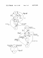
In the process and display mode, state 1 l of FIG. 10
and Table l, the display oscillator 404 and processor
oscillator 406 may be enabled simultaneously or alterna
tively the processor oscillator 406 only may be enabled.
This is particularly useful in the event that a long num
ber crunching routine is going to occur and a blank
display is undesirable for this length of time. The dis
play interface 416 can be updated in the process only
mode, and the system can then go to the process and
14
from the controller 400 of FIG. 9 forces the system to
change states to the display only mode, state 0 l of FIG.
11, as ‘described with reference to FIG. 10. Any opera
tive keycode (any key) forces a power up clear and a
state transition from state 0 1 display only mode to state
1 0 process only mode, as described with reference to
FIG. 10. In addition, in the system with timekeeping, a
request timekeep output from the timekeep counter
latch causes a power up clear to occur forcing a state
display mode so that the display will exhibit previously
transition from the display only mode 0 l to the process
updated data while the system is processing the number
only mode I 0.
crunching routine. While it is possible for the processor
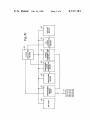
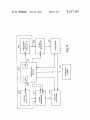
Referring to FIGS. 9 to 11, in a preferred mode, the
410 to communicate with the display interface 416 in
display oscillator 404 when enabled is operative at a
this mode, this will generally not be done except for
frequency of 50 Hz, and the main processor oscillator
quick input/output and K line communication since
406 when enabled is operative at a frequency of 1.6
enabling the main oscillator 406 only, will cause the
MHz or alternatively at a frequency of 500 KHz, de
display to blank. If a key is being held down after the
pending on the desired processor throughput.
system is ?nished processing it, the system will wait in
The system of FIG. 10 may be described as a master
the process and display mode (for calculators without
system controller which provides both processing and
the key rollover feature) for the key to be released 20 display control functions. In addition, the system inte
before returning to the display only mode. This is ac
grated circuit chip of FIG. 9 may exist without a display
complished by means of a software actuable any key
interface and therefore without a display oscillator. In
latch within the controller means 400, which when set
in response to instruction code set and reset signals will
this case, the system may be referred to as a slave con
troller system, as will be described with reference to the
pull all the select/R lines to VDD. The processor 410 25 state transition diagram of FIG. 12.
may then quickly scan the K lines to determine if a key
When the slave system is in an off state, state 0 0, the
is being held down. This sequence can generally be
appearance of an oscillator input causes a power up
done so quickly as to not affect the display. The se
clear to occur forcing the system to a process mode,
lect/R lines are interrupted and pulled to V55 in this
state I 0 FIG. 12. When the oscillator input is removed
mode also (every third common time for 125 microsec 30 (disappears) the system is forced to an off state, state 0
onds in a preferred embodiment) so that an off key
0 of FIG. 12.
(KD) can place the calculator in the off mode.
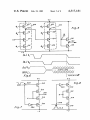
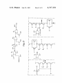
Referring to FIG. 13, a detailed schematic of an alter
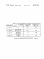
Referring to Table 2, instruction codes for the set
nate embodiment of the circuit group 50 of FIG. 3a and
display mode latch (DM), reset display mode latch
more specifically of a clocked CMOS circuit group
(DM), and off instructions are shown for the preferred 35 such as described with reference to FIGS. 7 and 8, is
embodiment.
shown. When the power consumption controller 51 of
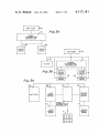
Referring to FIG. 11, a state transition diagram for
FIG. 3a forces the circuit group 52 to a standby low
the multimode power controller for a calculator system
power state, and clocks $4, (1);; and rbcof FIG. 13 are set
with timekeeping is shown. The state transitions in a
to the active logic level non-cycling state, all clocked
timekeeping application contain the same four modes as 40 gates are transformed to static gates, and all sequential
in the nontimekeeping application, as shown in FIG. 10,
logic to combinational logic, thereby allowing imposi
each mode serving the same function. A timekeeping
tion of a prede?ned output level. This requires that
overload register output will generate a power up clear
various critical input control nodes in the logic must be
and place the calculator system into the process only
forced to a fixed state so as to force the combinational
mode. In addition, as explained with reference to FIG. 45 logic to output a prede?ned voltage level. For example,
10, the on key operative key code (KA) generates a
if it is desired that node 500 be at a logical high level
power up clear so as to place the system in a process
during the standby state, node 502 must be set to a
only mode. In the timekeeping system, an additional
logical low level in the standby state. A preset output
means for going from the off mode, state 0 0 in FIG. 11,
504 from the power consumption controller 51 is cou
to the process only mode, State l 0 in FIG. 11, is accom
pled to one input of NOR gate 503. The output of NOR
plished in response to a request timekeep output from a
gate 503 is coupled to node 502, thereby effectively
counter latch in the timekeeping circuitry to provide for
controlling the forced state output at node 500. When
a periodic update of the timekeeping latches, every one
the preset output 504 is output at a high logic level
second in a preferred embodiment. As described above
during the standby state, the output of NOR gate 502
with reference to FIG. 10, a set display mode oscillator 55 will be forced to a logic low level irrespective of the
latch instruction code from the controller 400 of FIG. 9
logic level of signal e at input 505 of NOR gate 503.
causes the system of FIG. I] to go from the process
Thus, node 502 is forced to a logic low level in direct
only mode to the process and display mode, and a reset
response to a preset output 504 from the power con
display mode latch instruction code from the controller
sumption controller 51 and thereby forces a logical high
400 of FIG. 9 causes the system to go from a process 60 level output at node 500, as desired, irrespective of the
and display mode to a process only mode. In addition, a
other input signal levels. Thus, in response to the preset
timekeep overload output from a timekeeping overload
output from the power consumption controller 51. a
latch causes a power up clear to occur and forces a state
predefined output level is obtainable independent of the
transition to the process only mode. The timekeep over
active mode inputs 505, 506, or 507 to the logic circuitry
load output forces a power up clear, but when the sys 65 of FIG. 13. A significant advancement is achieved be
tem is already in the process only mode, no state transi
yond the standby power dissipation modes of ratiolcss
tion occurs. When the system is in the process and dis
precharge discharge logic shown in FIG. 5, or the
play mode, state I l of FIG. 11, an offinstruction code
clocked CMOS logic is shown in FIG. 7 and 8, by the