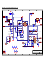
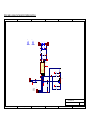
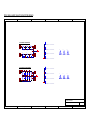
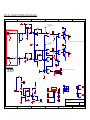
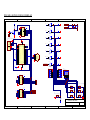
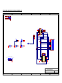
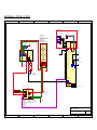
1
AVTECH
ELECTROSYSTEMS
N A N O S E C O N D
P.O. BOX 265
OGDENSBURG, NY
U.S.A. 13669-0265
W A V E F O R M E L E C T R O N I C S
S I N C E 1 9 7 5
TEL: 888-670-8729 (USA & Canada) or +1-613-226-5772 (Intl)
FAX: 800-561-1970 (USA & Canada) or +1-613-226-2802 (Intl)
[email protected]
-
LTD.
http://www.avtechpulse.com/
INSTRUCTIONS
MODEL AVR-GHV1-B
0 TO 500 Volts, 1 kHz PULSE GENERATOR
WITH IEEE 488.2 AND RS-232 CONTROL
SERIAL NUMBER: ____________
X
BOX 5120, LCD MERIVALE
OTTAWA, ONTARIO
CANADA K2C 3H4
2
WARRANTY
Avtech Electrosystems Ltd. warrants products of its manufacture to be free
from defects in material and workmanship under conditions of normal use. If,
within one year after delivery to the original owner, and after prepaid return by
the original owner, this Avtech product is found to be defective, Avtech shall at
its option repair or replace said defective item. This warranty does not apply to
units which have been dissembled, modified or subjected to conditions
exceeding the applicable specifications or ratings. This warranty is the extent of
the obligation assumed by Avtech with respect to this product and no other
warranty or guarantee is either expressed or implied.
TECHNICAL SUPPORT
Phone: 888-670-8729 (USA & Canada) or +1-613-226-5772 (Intl)
Fax: 800-561-1970 (USA & Canada) or +1-613-226-2802 (Intl)
E-mail: [email protected]
World Wide Web: http://www.avtechpulse.com
3
TABLE OF CONTENTS
WARRANTY.................................................................................................................... 2
TECHNICAL SUPPORT.................................................................................................. 2
TABLE OF CONTENTS.................................................................................................. 3
INTRODUCTION............................................................................................................. 5
AVAILABLE OPTIONS................................................................................................... 6
HIGH-VOLTAGE PRECAUTIONS.................................................................................. 7
SPECIFICATIONS........................................................................................................... 8
EUROPEAN REGULATORY NOTES............................................................................. 9
EC DECLARATION OF CONFORMITY....................................................................................9
DIRECTIVE 2002/95/EC (RoHS).............................................................................................. 9
DIRECTIVE 2002/96/EC (WEEE)..............................................................................................9
INSTALLATION............................................................................................................. 11
VISUAL CHECK...................................................................................................................... 11
POWER RATINGS.................................................................................................................. 11
CONNECTION TO THE POWER SUPPLY............................................................................ 11
PROTECTION FROM ELECTRIC SHOCK.............................................................................12
ENVIRONMENTAL CONDITIONS.......................................................................................... 12
LABVIEW DRIVERS............................................................................................................... 13
FUSES........................................................................................................................... 14
AC FUSE REPLACEMENT..................................................................................................... 14
DC FUSE REPLACEMENT..................................................................................................... 15
FUSE RATINGS...................................................................................................................... 15
FRONT PANEL CONTROLS........................................................................................ 16
REAR PANEL CONTROLS.......................................................................................... 18
GENERAL INFORMATION........................................................................................... 20
BASIC PULSE CONTROL...................................................................................................... 20
TRIGGER MODES.................................................................................................................. 22
PULSE WIDTH MODES.......................................................................................................... 22
GATING MODES..................................................................................................................... 22
OUTPUT IMPEDANCE............................................................................................................23
LOAD IMPEDANCE................................................................................................................ 23
BURST GENERATION (-BR OPTION)................................................................................... 23
4
PREVENTING OUTPUT STAGE FAILURE............................................................................ 25
OPERATIONAL CHECK............................................................................................... 26
PROGRAMMING YOUR PULSE GENERATOR........................................................... 29
KEY PROGRAMMING COMMANDS......................................................................................29
ALL PROGRAMMING COMMANDS...................................................................................... 30
MECHANICAL INFORMATION..................................................................................... 32
TOP COVER REMOVAL......................................................................................................... 32
RACK MOUNTING.................................................................................................................. 32
ELECTROMAGNETIC INTERFERENCE................................................................................32
MAINTENANCE............................................................................................................ 33
REGULAR MAINTENANCE.................................................................................................... 33
CLEANING.............................................................................................................................. 33
WIRING DIAGRAMS..................................................................................................... 34
WIRING OF AC POWER.........................................................................................................34
PCB 158K - LOW VOLTAGE POWER SUPPLY, 1/3.............................................................35
PCB 158K - LOW VOLTAGE POWER SUPPLY, 2/3.............................................................36
PCB 158K - LOW VOLTAGE POWER SUPPLY, 3/3.............................................................37
PCB 168B - HIGH VOLTAGE DC POWER SUPPLY............................................................. 38
PCB 183A-S AND 183A-P CAPACITOR BANKS...................................................................39
PCB 156 – POLARITY CONTROL (-PN UNITS ONLY)......................................................... 40
PCB 104D - KEYPAD / DISPLAY BOARD, 1/3...................................................................... 41
PCB 104D - KEYPAD / DISPLAY BOARD, 2/3...................................................................... 42
PCB 104D - KEYPAD / DISPLAY BOARD, 3/3...................................................................... 43
MAIN WIRING – POSITIVE (-P) UNITS..................................................................................44
MAIN WIRING – DUAL POLARITY (-PN) UNITS................................................................... 45
PERFORMANCE CHECK SHEET................................................................................ 46
Manual Reference: Z:\officefiles\instructword\avr-g\AVR-GHV1-B,edition2.odt.
Last modified July 13, 2006.
Copyright © 2006 Avtech Electrosystems Ltd, All Rights Reserved.
5
INTRODUCTION
The AVR-GHV1-B is a high performance, GPIB and RS232-equipped instrument
capable of generating 0 to 500V at repetition rates up to 1 kHz into high-impedance
loads of 100 kΩ or higher. The pulse width is variable from 200 ns to 500 ms, and the
duty cycle may be as high as 80%. Rise and fall times are fixed at less than 40 ns. The
AVR-GHV1-B includes an internal trigger source, but it can also be triggered or gated
by an external source. A front-panel pushbutton can also be used to trigger the
instrument. The output pulse width can be set to follow an input trigger pulse width.
The output voltage polarity depends on the model number:
"-P" units: 0 to +500 Volts
"-N" units: 0 to -500 Volts
"-PN" units: 0 to ±500 Volts
The AVR-GHV1-B features front panel keyboard and adjust knob control of the output
pulse parameters along with a four line by 40-character backlit LCD display of the
output amplitude, pulse width, pulse repetition frequency, and delay. The instrument
includes memory to store up to four complete instrument setups. The operator may use
the front panel or the computer interface to store a complete “snapshot” of all key
instrument settings, and recall this setup at a later time.
The instrument is protected against overload conditions (such as short circuits) by an
automatic control circuit. An internal power supply monitor removes the power to the
output stage for five seconds if an average power overload exists. After that time, the
unit operates normally for one second, and if the overload condition persists, the power
is cut again. This cycle repeats until the overload is removed.
This instrument is intended for use in research, development, test and calibration
laboratories by qualified personnel.
6
AVAILABLE OPTIONS
-BR Option:
This optional feature allows a burst of 1-500 pulses to be generated in
response to each trigger event.
-HN Option: The standard N-type output connector is replaced with an HN-type
connector.
-MHV Option: The standard N-type output connector is replaced with an MHV-type
connector.
-SHV Option: The standard N-type output connector is replaced with an SHV-type
connector.
-R5 Option: Rack-mount kit.
-TNT Option:
Adds a rear-panel Ethernet connector, providing Telnet-based remote
control from a network.
7
HIGH-VOLTAGE PRECAUTIONS
CAUTION: This instrument provides output voltages as high as 500 Volts under
normal operating conditions, and generates up to 530V internally, so extreme caution
must be employed when using this instrument. The instrument should only be used by
individuals who are thoroughly skilled in high voltage laboratory techniques. The
following precautions should always be observed:
1) Keep exposed high-voltage wiring to an absolute minimum.
2) Wherever possible, use shielded connectors and cabling.
3) Connect and disconnect loads and cables only when the instrument is turned off.
4) Keep in mind that all cables, connectors, oscilloscope probes, and loads must
have an appropriate voltage rating.
Do not attempt any repairs on the instrument, beyond the fuse replacement procedures
described in this manual. Contact Avtech technical support (see page 2 for contact
information) if the instrument requires servicing.
8
SPECIFICATIONS
Model:
AVR-GHV1-B1
Amplitude:
0 to 500 Volts
Pulse width (FWHM) :
2
Load impedance:
200 ns to 0.5 sec
≥ 100 kΩ
Output impedance:
50 Ω (i.e., internal resistance in series with the output).
7
Rise time (20%-80%) :
≤ 40 ns
Fall time (80%-20%) :
≤ 40 ns
7
PRF:
Duty cycle:
Polarity3:
GPIB and RS-232 control1:
LabView Drivers:
Telnet / Ethernet control4:
Burst mode:
1 Hz to 1 kHz
0 - 80 %
Positive or negative or both (specify)
Standard on -B units
Check http://www.avtechpulse.com/labview for availability and downloads
Optional on -B units. See http://www.avtechpulse.com/options/tnt for
details.
Optional5. Generates 1-500 pulses per trigger event. See
http://www.avtechpulse.com/options/br.
Propagation delay:
≤ 100 ns (Ext trig in to pulse out)
Jitter (Ext trig in to pulse out):
± 100 ps ± 0.03% of sync delay
Trigger required:
(External trigger modes)
Mode A: + 5 Volt, > 50 ns (TTL)
Mode B: + 5 Volt, PW IN = PW OUT (TTL)
Sync delay:
Variable, 0 to ± 1 second
Sync output:
+ 3 Volts, 100 ns, will drive 50 Ohm loads
Gate input:
Connectors (OUT)6:
Connectors (Trig, Sync, Gate):
Power requirements:
Dimensions (H x W x D):
Synchronous or asynchronous, active high or low, switchable.
Suppresses triggering when active.
Type N
BNC
100 - 240 Volts, 50 - 60 Hz
100 mm x 430 mm x 375 mm (3.9” x 17” x 14.8”)
Chassis material:
cast aluminum frame and handles, blue vinyl on aluminum cover plates
Mounting:
Any. Add the suffix -R5 to the model number to include a rack-mount kit.
Temperature range:
+5°C to +40°C
1) -B suffix indicates IEEE-488.2 GPIB and RS-232 control of amplitude, pulse width or duty cycle (as appropriate), pulse repetition frequency, and delay
(See http://www.avtechpulse.com/gpib).
2) When triggered externally, the pulse width can be set by the pulse instrument controls, or it may be set to track the input trigger pulse width.
3) Indicate desired polarity by suffixing model number with -P or -N (i.e. positive or negative) or -PN for dual polarity option (controlled by a two-position
switch which controls the polarity of the signal output port). Keypad polarity control on -B units.
4) Add the suffix -TNT to the model number to specify the Telnet / Ethernet control option.
5) Add the suffix -BR to the model number to specify the burst mode option. See http://www.avtechpulse.com/options/br for details about this option.
6) HV, MHV or HN output connectors can also be provided. To specify, suffix the model number by -SHV, -MHV or -HN as required.
7) Valid when the load is connected with zero cable length (for instance, on a binding post adapter). The rise and fall times will degrade for non-zero
lengths of cable, due to the product of the 50 Ohm output impedance and the cable capacitance. The maximum cable length for operation (with
degraded rise and fall times) is 2 meters (6 feet). If your application requires longer cable lengths, contact Avtech for appropriate modifications or
applications assistance.
9
EUROPEAN REGULATORY NOTES
EC DECLARATION OF CONFORMITY
We
Avtech Electrosystems Ltd.
P.O. Box 5120, LCD Merivale
Ottawa, Ontario
Canada K2C 3H4
declare that this pulse generator meets the intent of Directive 89/336/EEC for
Electromagnetic Compatibility. Compliance pertains to the following specifications as
listed in the official Journal of the European Communities:
EN 50081-1 Emission
EN 50082-1 Immunity
and that this pulse generator meets the intent of the Low Voltage Directive 72/23/EEC
as amended by 93/68/EEC. Compliance pertains to the following specifications as listed
in the official Journal of the European Communities:
EN 61010-1:2001
Safety requirements for electrical equipment for
measurement, control, and laboratory use
DIRECTIVE 2002/95/EC (RoHS)
This instrument is exempt from Directive 2002/95/EC of the European Parliament and
of the Council of 27 January 2003 on the Restriction of the use of certain Hazardous
Substances (RoHS) in electrical and electronic equipment. Specifically, Avtech
instruments are considered "Monitoring and control instruments" (Category 9) as
defined in Annex 1A of Directive 2002/96/EC. The Directive 2002/95/EC only applies to
Directive 2002/96/EC categories 1-7 and 10, as stated in the "Article 2 - Scope" section
of Directive 2002/95/EC.
DIRECTIVE 2002/96/EC (WEEE)
European customers who have purchased this equipment directly from Avtech will have
completed a “WEEE Responsibility Agreement” form, accepting responsibility for
10
WEEE compliance (as mandated in Directive 2002/96/EC of the European Union and
local laws) on behalf of the customer, as provided for under Article 9 of Directive
2002/96/EC.
Customers who have purchased Avtech equipment through local representatives
should consult with the representative to determine who has responsibility for WEEE
compliance. Normally, such responsibilities with lie with the representative, unless other
arrangements (under Article 9) have been made.
Requirements for WEEE compliance may include registration of products with local
governments, reporting of recycling activities to local governments, and financing of
recycling activities.
11
INSTALLATION
VISUAL CHECK
After unpacking the instrument, examine to ensure that it has not been damaged in
shipment. Visually inspect all connectors, knobs, liquid crystal displays (LCDs), and the
handles. Confirm that a power cord, a GPIB cable, and two instrumentation manuals
(this manual and the “Programming Manual for -B Instruments”) are with the instrument.
If the instrument has been damaged, file a claim immediately with the company that
transported the instrument.
POWER RATINGS
This instrument is intended to operate from 100 - 240 V, 50 - 60 Hz.
The maximum power consumption is 57 Watts. Please see the “FUSES” section for
information about the appropriate AC and DC fuses.
This instrument is an “Installation Category II” instrument, intended for operation from a
normal single-phase supply.
CONNECTION TO THE POWER SUPPLY
An IEC-320 three-pronged recessed male socket is provided on the back panel for AC
power connection to the instrument. One end of the detachable power cord that is
supplied with the instrument plugs into this socket. The other end of the detachable
power cord plugs into the local mains supply. Use only the cable supplied with the
instrument. The mains supply must be earthed, and the cord used to connect the
instrument to the mains supply must provide an earth connection. (The supplied cord
does this.)
Warning: Failure to use a grounded outlet may result in injury or death due to
electric shock. This product uses a power cord with a ground connection. It must be
connected to a properly grounded outlet. The instrument chassis is connected to the
ground wire in the power cord.
The table below describes the power cord that is normally supplied with this instrument,
depending on the destination region:
12
Destination Region
Description
Manufacturer
Part Number
Continental Europe
European CEE 7/7
“Schuko” 230V, 50Hz
Volex (http://www.volex.com)
17850-C3-326
Qualtek (http://www.qualtekusa.com)
319004-T01
United Kingdom
BS 1363,
230V, 50Hz
Qualtek (http://www.qualtekusa.com)
370001-E01
Switzerland
SEV 1011, 2
30V, 50Hz
Volex (http://www.volex.com)
2102H-C3-10
Israel
SI 32,
220V, 50Hz
Volex (http://www.volex.com)
2115H-C3-10
North America,
and all other areas
NEMA 5-15,
120V, 60 Hz
Qualtek (http://www.qualtekusa.com)
312007-01
PROTECTION FROM ELECTRIC SHOCK
Operators of this instrument must be protected from electric shock at all times. The
owner must ensure that operators are prevented access and/or are insulated from
every connection point. In some cases, connections must be exposed to potential
human contact. Operators must be trained to protect themselves from the risk of
electric shock. This instrument is intended for use by qualified personnel who recognize
shock hazards and are familiar with safety precautions required to avoid possibly injury.
In particular, operators should:
1) Keep exposed high-voltage wiring to an absolute minimum.
2) Wherever possible, use shielded connectors and cabling.
3) Connect and disconnect loads and cables only when the instrument is turned off.
4) Keep in mind that all cables, connectors, oscilloscope probes, and loads must
have an appropriate voltage rating.
5) Do not attempt any repairs on the instrument, beyond the fuse replacement
procedures described in this manual. Contact Avtech technical support (see
page 2 for contact information) if the instrument requires servicing. Service is to
be performed solely by qualified service personnel.
ENVIRONMENTAL CONDITIONS
This instrument is intended for use under the following conditions:
1) indoor use;
2) altitude up to 2 000 m;
3) temperature 5 °C to 40 °C;
13
4) maximum relative humidity 80 % for temperatures up to 31 °C decreasing
linearly to 50 % relative humidity at 40 °C;
5) Mains supply voltage fluctuations up to ±10 % of the nominal voltage;
6) no pollution or only dry, non-conductive pollution.
LABVIEW DRIVERS
A LabVIEW driver for this instrument is available for download on the Avtech web site,
at http://www.avtechpulse.com/labview. A copy is also available in National Instruments'
Instrument Driver Library at http://www.natinst.com/.
14
FUSES
This instrument contains four fuses. All are accessible from the rear-panel. Two protect
the AC prime power input, and two protect the internal DC power supplies. The
locations of the fuses on the rear panel are shown in the figure below:
Fuses #1 and #2
(AC fuses)
Fuse #4
(DC fuse)
Fuse #3
(DC fuse)
AC FUSE REPLACEMENT
To physically access the AC fuses, the power cord must be detached from the rear
panel of the instrument. The fuse drawer may then be extracted using a small flat-head
screwdriver, as shown below:
Pry out the fuse
drawer using a
screwdriver.
Fuse
Drawer
15
DC FUSE REPLACEMENT
The DC fuses may be replaced by inserting the tip of a flat-head screwdriver into the
fuse holder slot, and rotating the slot counter-clockwise. The fuse and its carrier will
then pop out.
FUSE RATINGS
The following table lists the required fuses:
Fuses
Nominal
Mains
Voltage
#1, #2 (AC) 100-240V
#3 (DC)
N/A
#4 (DC)
N/A
Rating
0.5A, 250V,
Time-Delay
1.6A, 250V,
Time-Delay
0.5A, 250V,
Time-Delay
Recommended Replacement Part
Case Size Littelfuse Part
Digi-Key Stock
Number
Number
5×20 mm
0218.500HXP
F2416-ND
5×20 mm
021801.6HXP
F2424-ND
5×20 mm
0218.500HXP
F2416-ND
The recommended fuse manufacturer is Littelfuse (http://www.littelfuse.com).
Replacement fuses may be easily obtained from Digi-Key (http://www.digikey.com) and
other distributors.
16
FRONT PANEL CONTROLS
1
2
3
6
5
4
1. POWER Switch. This is the main power switch. When turning the instrument on,
there may be a delay of several seconds before the instrument appears to respond.
2. OVERLOAD Indicator. When the instrument is powered, this indicator is normally
green, indicating normal operation. If this indicator is yellow, an internal automatic
overload protection circuit has been tripped. If the unit is overloaded (by operating at
an exceedingly high duty cycle or by operating into a very low impedance), the
protective circuit will disable the output of the instrument and turn the indicator light
yellow. The light will stay yellow (i.e. output disabled) for about 5 seconds after
which the instrument will attempt to re-enable the output (i.e. light green) for about 1
second. If the overload condition persists, the output will be disabled again (i.e. light
yellow) for another 5 seconds. If the overload condition has been removed, the
instrument will resume normal operation.
This overload indicator may flash yellow briefly at start-up. This is not a cause for
concern.
3. OUT CONNECTOR. This N-type connector provides the output to a 100 kΩ (or
higher) load.
Caution: Voltages as high as ±500V may be present on the center conductor of
this output connector. Avoid touching this conductor. Connect to this connector
using standard coaxial cable, to ensure that the center conductor is not exposed.
4. SYNC OUT. This connector supplies a SYNC output that can be used to trigger
other equipment, particularly oscilloscopes. This signal leads (or lags) the main
output by a duration set by the "DELAY" controls and has an approximate amplitude
of +3 Volts to RL > 1kΩ with a pulse width of approximately 100 ns.
5. LIQUID CRYSTAL DISPLAY (LCD). This LCD is used in conjunction with the
keypad to change the instrument settings. Normally, the main menu is displayed,
which lists the key adjustable parameters and their current values. The
17
“Programming Manual for -B Instruments” describes the menus and submenus in
detail.
6. KEYPAD.
Control Name
MOVE
CHANGE
×10
÷10
+/EXTRA FINE
ADJUST
Function
This moves the arrow pointer on the display.
This is used to enter the submenu, or to select the operating
mode, pointed to by the arrow pointer.
If one of the adjustable numeric parameters is displayed, this
increases the setting by a factor of ten.
If one of the adjustable numeric parameters is displayed, this
decreases the setting by a factor of ten.
If one of the adjustable numeric parameters is displayed, and
this parameter can be both positive or negative, this changes the
sign of the parameter.
This changes the step size of the ADJUST knob. In the extrafine mode, the step size is twenty times finer than in the normal
mode. This button switches between the two step sizes.
This large knob adjusts the value of any displayed numeric
adjustable values, such as frequency, pulse width, etc. The
adjust step size is set by the "EXTRA FINE" button.
When the main menu is displayed, this knob can be used to
move the arrow pointer.
18
REAR PANEL CONTROLS
4
5
8
GATE
LAN
1
3
GRN=LNK
YEL=ACT
TRIG
RS-232
AMP
GPIB
9
6
7
2
1. AC POWER INPUT. An IEC-320 C14 three-pronged recessed male socket is
provided on the back panel for AC power connection to the instrument. One end of
the detachable power cord that is supplied with the instrument plugs into this socket.
2. AC FUSE DRAWER. The two fuses that protect the AC input are located in this
drawer. Please see the “FUSES” section of this manual for more information.
3. DC FUSES. These two fuses protect the internal DC power supplies. Please see the
“FUSES” sections of this manual for more information.
4. GATE. This TTL-level (0 and +5V) logic input can be used to gate the triggering of
the instrument. This input can be either active high or active low, depending on the
front panel settings or programming commands. (The instrument triggers normally
when this input is unconnected). When set to active high mode, this input is pulleddown to ground by a 1 kΩ resistor. When set to active low mode, this input is pulledup to +5V by a 1 kΩ resistor.
5. TRIG. This TTL-level (0 and +5V) logic input can be used to trigger the instrument, if
the instrument is set to triggering externally. The instrument triggers on the rising
edge of this input. The input impedance of this input is 1 kΩ. (Depending on the
length of cable attached to this input, and the source driving it, it may be desirable to
add a coaxial 50 Ohm terminator to this input to provide a proper transmission line
termination. The Pasternack (www.pasternack.com) PE6008-50 BNC feed-thru 50
Ohm terminator is suggested for this purpose.)
When triggering externally, the instrument can be set such that the output pulse
width tracks the pulse width on this input, or the output pulse width can be set
independently.
19
6. GPIB Connector. A standard GPIB cable can be attached to this connector to allow
the instrument to be computer-controlled. See the “Programming Manual for -B
Instruments” for more details on GPIB control.
7. RS-232 Connector. A standard serial cable with a 25-pin male connector can be
attached to this connector to allow the instrument to be computer-controlled. See the
“Programming Manual for -B Instruments” for more details on RS-232 control.
8. LAN Connector and Indicator. (Optional feature. Present on -TNT units only.) The
-TNT option "Internet-enables" Avtech pulse generators by adding this standard
Ethernet port to the rear panel, in addition to the IEEE-488.2 GPIB and RS-232 ports
normally found on "-B" units. Commands are sent using the standard Telnet protocol.
The SCPI-compliant command set is the same as that used for GPIB and RS-232
control. The -TNT option uses the Dynamic Host Configuration Protocol (DHCP) to
obtain its network address. A DHCP server must be present on the local network for
the -TNT option to operate properly.
9. AMP Connector. This connector, if present, is not used.
20
GENERAL INFORMATION
BASIC PULSE CONTROL
This instrument can be triggered by its own internal clock or by an external TTL trigger
signal. In either case, two output channels respond to the trigger: OUT and SYNC. The
OUT channel is the signal that is applied to the load. Its amplitude and pulse width are
variable. The SYNC pulse is a fixed-width TTL-level reference pulse used to trigger
oscilloscopes or other measurement systems. When the delay is set to a positive value
the SYNC pulse precedes the OUT pulse. When the delay is set to a negative value the
SYNC pulse follows the OUT pulse.
These pulses are illustrated below, assuming internal triggering and a positive delay:
SYNC OUT
(generated by the
internal oscillator)
100 ns, FIXED
3V, FIXED
DELAY > 0
PULSE WIDTH
AMPLITUDE,
VARIABLE
MAIN OUTPUT
Figure A
If the delay is negative, the order of the SYNC and OUT pulses is reversed:
100 ns, FIXED
SYNC OUT
(generated by the
internal oscillator)
3V, FIXED
DELAY < 0
PULSE WIDTH
AMPLITUDE,
VARIABLE
MAIN OUTPUT
Figure B
The next figure illustrates the relationship between the signal when an external TTLlevel trigger is used:
21
> 50 ns
TRIG
(external input)
TTL LEVELS
(0V and 3V-5V)
PROPAGATION DELAY (FIXED)
100 ns, FIXED
SYNC OUT
3V, FIXED
DELAY > 0
PULSE WIDTH
AMPLITUDE,
VARIABLE
MAIN OUTPUT
Figure C
As before, if the delay is negative, the order of the SYNC and OUT pulses is reversed.
The last figure illustrates the relationship between the signal when an external TTL-level
trigger is used in the PW IN=PW OUT mode. In this case, the output pulse width equals the
external trigger’s pulse width (approximately), and the delay circuit is bypassed:
PW IN
TRIG
(external input)
TTL LEVELS
(0V and 3V-5V)
PROPAGATION DELAY (FIXED)
PW OUT ≈ PW IN
AMPLITUDE,
VARIABLE
MAIN OUTPUT
Figure D
The delay, pulse width, and frequency (when in the internal mode), of the OUT pulse
can be varied with front panel controls or via the GPIB or RS-232 computer interfaces.
22
TRIGGER MODES
This instrument has four trigger modes:
•
Internal Trigger: the instrument controls the trigger frequency, and generates the
clock internally.
•
External Trigger: the instrument is triggered by an external TTL-level clock on the
back-panel TRIG connector.
•
Manual Trigger: the instrument is triggered by the front-panel “SINGLE PULSE”
pushbutton.
•
Hold Trigger: the instrument is set to not trigger at all.
These modes can be selected using the front panel trigger menu, or by using the
appropriate programming commands. (See the “Programming Manual for -B
Instruments” for more details.)
PULSE WIDTH MODES
This instrument has two pulse width modes:
•
Normal: the instrument controls the output pulse width.
•
PW IN=PW OUT: the output pulse width equals the pulse width of the trigger signal on
the “TRIG” connector. The instrument must be in the external trigger mode.
These modes can be selected using the front panel pulse width menu, or by using the
appropriate programming commands. (See the “Programming Manual for -B
Instruments” for more details.)
GATING MODES
Triggering can be suppressed by a TTL-level signal on the rear-panel GATE connector.
The instrument can be set to stop triggering when this input high or low, using the frontpanel gate menu or the appropriate programming commands. This input can also be
set to act synchronously or asynchronously. When set to asynchronous mode, the
GATE will disable the output immediately. Output pulses may be truncated. When set
to synchronous mode, the output will complete the full pulse width if the output is high,
and then stop triggering. No pulses are truncated in this mode.
23
OUTPUT IMPEDANCE
The AVR-GHV1-B has an output impedance (i.e., an internal resistance in series with
the output) of 50 Ohms, to provide transmission line back-matching and short-circuit
protection.
The rise and fall times are fixed at less than 40 ns. However, since the output
impedance is 50Ω, the rise and fall times will degrade if cable lengths longer than 1
meter (3 feet) are used on the output, due to the cable capacitance. The maximum
usable cable length is 2 meters (6 feet).
LOAD IMPEDANCE
The AVR-GHV1-B can drive load impedances of 100 kΩ or higher. It is NOT designed
to drive 50 Ω loads or highly capacitive loads. (The AVR-GHV1-B is tested with
capacitive loads of 330 pF. Load capacitance should not exceed 330 pF.)
BURST GENERATION (-BR OPTION)
The waveforms given above assume that a single output pulse is generated for each
trigger event (regardless of the source). However, when the burst mode feature is used
on units with the -BR option, the instrument can generate 1-500 pulses for each
individual trigger event. The number of output pulses in each burst can be adjusted
from 1 to 500 using the front-panel controls (using the “N” menu), or by a computer
command. The time between pulses (i.e., from the falling edge of one pulse to the
rising edge of the next pulse) can also varied from 1 ms to 1.0 seconds from the front
panel (using the “BUR” menu), or by computer command.
The figure below shows burst mode operation (i.e., N > 1) used with internal triggering:
PERIOD = 1 / FREQUENCY
SYNC OUT
(generated by the
internal oscillator)
DELAY
(VARIABLE)
PULSE WIDTH
(VARIABLE)
BURST COUNT (N),
VARIABLE FROM 1 TO 500.
(N = 3, IN THIS EXAMPLE)
MAIN OUTPUT
BURST PULSE
SEPARATION
The figure below shows burst mode operation used with external triggering:
24
> 50 ns
TRIG
(external input)
TTL LEVELS
(0 and 3V-5V)
PROPAGATION DELAY (FIXED)
SYNC OUT
DELAY
(VARIABLE)
PULSE WIDTH
(VARIABLE)
BURST COUNT (N),
VARIABLE FROM 1 TO 500.
(N = 3, IN THIS EXAMPLE)
MAIN OUTPUT
BURST PULSE
SEPARATION
The burst mode may also be used with the front-panel “Single Pulse” pushbutton as a
trigger source. (Pressing the pushbutton will actually generate a single burst, rather
than a single pulse, in this mode.) Computer commands can also trigger a burst.
To control the burst count and timing from the front-panel, use the “N” and “BUR”
menus. To control them using computer commands, use the SOURce:PULSe:COUNt
and SOURce:PULSe:SEParation commands, as described in the programming manual.
The pulse spacing is constrained by several factors:
1. The maximum PRF limitation of the instrument applies within the burst. That is,
timing between two consecutive leading edges must lie between a minimum of
1/PRFMAX and a maximum of 1.0 seconds, where PRFMAX is the maximum
pulse repetition frequency specification for the instrument.
For this instrument, the maximum PRF for the instrument is 1 kHz, so the time
between two leading edges within the burst may not be smaller than 1
millisecond. The total number of pulses per second (i.e., Trigger Frequency x
Burst Count) must also be less than 1 kHz.
2. The maximum duty cycle limitation of the instrument can not be exceeded inside
the burst. Within the burst, the duty cycle may be calculated using DCBURST =
100% x Pulse Width / (Pulse Width + Pulse Separation). The total average duty
cycle is equal to DCAVG = 100% x Pulse Width x Burst Count x Trigger
Frequency. Both DCBURST and DCAVG must be less than the rated maximum
duty cycle of the instrument.
For this instrument, the maximum duty cycle is 80%.
25
PREVENTING OUTPUT STAGE FAILURE
The output stage is protected against overload conditions by an overload circuit and
fuses on the main frame back panel. However, the output switching elements may fail if
the unit is triggered at a PRF exceeding 1 kHz or if the load impedance is too low (<
100 kΩ or > 330 pF). Heating and subsequent possible failure of the output stage is
reduced if the following action is taken where possible:
•
PRF is kept to a minimum, i.e. operate in a low PRF range when possible rather
than in a high PRF range.
•
Keep the output PW to a minimum.
•
Never apply an externally generated voltage to the output port.
•
Reduce the amplitude below 100 Volts before changing the output polarity. Note
that internal protection circuits will prevent the polarity from switching when the
amplitude is set higher than ±100V, until the internal power supplies have
discharged the voltage on the internal energy-storage capacitors to below ±100V.
This may take several seconds.
•
Use the correct load impedance (> 100 kΩ and < 330 pF).
•
Keep output cable lengths to 2 meters (6 feet) or less.
26
OPERATIONAL CHECK
This section describes a sequence to confirm the basic operation of the instrument. It
should be performed after receiving the instrument. It is a useful learning exercise as
well.
Before proceeding with this procedure, finish read this instruction manual thoroughly.
Then read the “Local Control” section of the “Programming Manual for -B Instruments”
thoroughly. The “Local Control” section describes the front panel controls used in this
operational check - in particular, the MOVE, CHANGE, and ADJUST controls.
REAL-TIME
OSCILLOSCOPE
AVTECH
PULSER
MAIN OUTPUT
CONNECTOR
SCOPE
PROBE
CHANNEL A
TEST
LOAD
AC
POWER
SYNC
OUTPUT
TRIG
INPUT
ALL CABLES: 50 OHM COAXIAL
1. Connect a cable from the SYNC OUT connector to the TRIG input of an
oscilloscope. Connect a 100 kΩ (or higher) load to the OUT connector and place
the scope probe across this load. The load resistor must have a voltage rating of at
least 500V. The power dissipated in the resistor is given by
P = (V2 / R) × (PW / T) = (V2 / R) × PW × f
where “V” is the output voltage, “R” is the load resistance, “PW” is the pulse width,
and “T” is the pulse period (1/frequency), and “f” is the frequency. If a 100 kΩ
resistor is used, the worst-case power dissipation is 2.5 Watts. (Ohmite “OY”
ceramic composition resistors - http://www.ohmite.com - are recommended for such
applications. These resistors are readily available from http://www.digi-key.com/
and other distributors.)
2. Set the oscilloscope to trigger externally with the vertical setting at 100 Volts/div
and the horizontal setting at 1 us/div. Be sure that your oscilloscope and probe
setup can handle the maximum amplitude of 500V. A high-voltage attenuator might
be necessary to avoid damaging the probe and oscilloscope.
27
3. Turn on the AVR-GHV1-B. The main menu will appear on the LCD.
4. To set the AVR-GHV1-B to trigger from the internal clock at a PRF of 1 kHz:
The arrow pointer should be pointing at the frequency menu item. If it is not, press
the MOVE button until it is.
Press the CHANGE button. The frequency submenu will appear. Rotate the
ADJUST knob until the frequency is set at 1 kHz.
The arrow pointer should be pointing at the “Internal” choice. If it is not, press
MOVE until it is.
Press CHANGE to return to the main menu.
5. To set the delay to 1 us:
Press the MOVE button until the arrow pointer is pointing at the delay menu item.
Press the CHANGE button. The delay submenu will appear. Rotate the ADJUST
knob until the delay is set at 1 us.
The arrow pointer should be pointing at the “Normal” choice. If it is not, press
MOVE until it is.
Press CHANGE to return to the main menu.
6. To set the pulse width to 1 us:
Press the MOVE button until the arrow pointer is pointing at the pulse width menu
item.
Press the CHANGE button. The pulse width submenu will appear. Rotate the
ADJUST knob until the pulse width is set at 1 us.
The arrow pointer should be pointing at the “Normal” choice. If it is not, press
MOVE until it is.
Press CHANGE to return to the main menu.
7. At this point, nothing should appear on the oscilloscope.
8. To enable the output:
Press the MOVE button until the arrow pointer is pointing at the output menu item.
Press the CHANGE button. The output submenu will appear.
28
Press MOVE until the arrow pointer is pointing at the “ON” choice.
Press CHANGE to return to the main menu.
9. To change the output amplitude:
Press the MOVE button until the arrow pointer is pointing at the amplitude menu
item.
Press the CHANGE button. The amplitude submenu will appear. Rotate the
ADJUST knob until the amplitude is set at +200V (or -200V for "-N" instruments).
Observe the oscilloscope. You should see 1 us wide, 200V pulses.
Rotate the ADJUST knob. The amplitude as seen on the oscilloscope should vary.
Reduce the amplitude to 50V (or -50V for "-N" instruments), using the adjust knob.
For "-PN" units only: Change the output polarity by pressing the “+/-” button. The
output amplitude should become negative, and you should see -50V pulses on
the oscilloscope. (Avoid switching polarity when the amplitude is higher than
100V. Reduce the amplitude first.)
Rotate the ADJUST knob. The amplitude as seen on the oscilloscope should vary.
Press CHANGE to return to the main menu.
10. Repeat step 9, but set the amplitude to zero.
11. This completes the operational check.
29
PROGRAMMING YOUR PULSE GENERATOR
KEY PROGRAMMING COMMANDS
The “Programming Manual for -B Instruments” describes in detail how to connect the
pulse generator to your computer, and the programming commands themselves. A
large number of commands are available; however, normally you will only need a few of
these. Here is a basic sample sequence of commands that might be sent to the
instrument after power-up:
*rst
trigger:source internal
frequency 1000 Hz
pulse:width 1 us
pulse:delay 2 us
volt 200
output on
(resets the instrument)
(selects internal triggering)
(sets the frequency to 1000 Hz)
(sets the pulse width to 1 us)
(sets the delay to 2 us)
(sets the amplitude to 200 V)
(turns on the output)
For triggering a single event, this sequence would be more appropriate:
*rst
trigger:source hold
pulse:width 1 us
pulse:delay 2 us
output on
volt 200
trigger:source immediate
trigger:source hold
output off
(resets the instrument)
(turns off all triggering)
(sets the pulse width to 1 us)
(sets the delay to 2 us)
(turns on the output)
(sets the amplitude to 200 V)
(generates a single non-repetitive trigger event)
(turns off all triggering)
(turns off the output)
To set the instrument to trigger from an external TTL signal applied to the rear-panel
TRIG connector, use:
*rst
trigger:source external
pulse:width 1 us
pulse:delay 2 us
volt 200
output on
(resets the instrument)
(selects internal triggering)
(sets the pulse width to 1 us)
(sets the delay to 2 us)
(sets the amplitude to 200 V)
(turns on the output)
These commands will satisfy 90% of your programming needs.
30
ALL PROGRAMMING COMMANDS
For more advanced programmers, a complete list of the available commands is given
below. These commands are described in detail in the “Programming Manual for -B
Instruments”. (Note: this manual also includes some commands that are not
implemented in this instrument. They can be ignored.)
Keyword
LOCAL
OUTPut:
:[STATe]
:PROTection
:TRIPped?
REMOTE
[SOURce]:
:FREQuency
[:CW | FIXed]
[SOURce]:
:PULSe
:PERiod
:WIDTh
:DCYCle
:HOLD
:DELay
:GATE
:TYPE
:LEVel
[SOURce]:
:VOLTage
[:LEVel]
[:IMMediate]
[:AMPLitude]
:PROTection
:TRIPped?
STATUS:
:OPERation
:[EVENt]?
:CONDition?
:ENABle
:QUEStionable
:[EVENt]?
:CONDition?
:ENABle
SYSTem:
:COMMunicate
:GPIB
:ADDRess
:SERial
:CONTrol
:RTS
:[RECeive]
:BAUD
:BITS
:ECHO
:PARity
:[TYPE]
Parameter
Notes
<boolean value>
[query only]
<numeric value>
<numeric value>
<numeric value> | EXTernal
<numeric value>
WIDTh | DCYCle
<numeric value>
ASYNC | SYNC
HIgh | LOw
<numeric value> | EXTernal
[query only]
<numeric value>
[query only, always returns "0"]
[query only, always returns "0"]
[implemented but not useful]
<numeric value>
[query only, always returns "0"]
[query only, always returns "0"]
[implemented but not useful]
<numeric value>
ON | IBFull | RFR
1200 | 2400 | 4800 | 9600
7|8
<boolean value>
EVEN | ODD | NONE
31
:SBITS
:ERRor
:[NEXT]?
:COUNT?
:VERSion?
TRIGger:
:SOURce
*CLS
*ESE
*ESR?
*IDN?
*OPC
*SAV
*RCL
*RST
*SRE
*STB?
*TST?
*WAI
1|2
[query only]
[query only]
[query only]
INTernal | EXTernal | MANual | HOLD | IMMediate
[no query form]
<numeric value>
[query only]
[query only]
0|1|2|3
0|1|2|3
<numeric value>
[no query form]
[no query form]
[no query form]
[query only]
[query only]
[no query form]
32
MECHANICAL INFORMATION
TOP COVER REMOVAL
If necessary, the interior of the instrument may be accessed by removing the four
Phillips screws on the top panel. With the four screws removed, the top cover may be
slid back (and off).
Always disconnect the power cord and allow the instrument to sit unpowered for 10
minutes before opening the instrument. This will allow any internal stored charge to
discharge.
There are no user-adjustable internal circuits. For repairs other than fuse replacement,
please contact Avtech ([email protected]) to arrange for the instrument to be
returned to the factory for repair. Service is to be performed solely by qualified service
personnel.
Caution: High voltages are present inside the instrument during normal operation.
Do not operate the instrument with the cover removed.
RACK MOUNTING
A rack mounting kit is available. The -R5 rack mount kit may be installed after first
removing the one Phillips screw on the side panel adjacent to the front handle.
ELECTROMAGNETIC INTERFERENCE
To prevent electromagnetic interference with other equipment, all used outputs should
be connected to shielded loads using shielded coaxial cables. Unused outputs should
be terminated with shielded coaxial terminators or with shielded coaxial dust caps, to
prevent unintentional electromagnetic radiation. All cords and cables should be less
than 3m in length.
33
MAINTENANCE
REGULAR MAINTENANCE
This instrument does not require any regular maintenance.
On occasion, one or more of the four rear-panel fuses may require replacement. All
fuses can be accessed from the rear panel. See the “FUSES” section for details.
CLEANING
If desired, the interior of the instrument may be cleaned using compressed air to
dislodge any accumulated dust. (See the “TOP COVER REMOVAL” section for
instructions on accessing the interior.) No other cleaning is recommended.
WIRING DIAGRAMS
WIRING OF AC POWER
3
Do not attempt any repairs on this instrument
beyond the fuse replacement procedures described
in the manual. Contact Avtech if the instrument
requires servicing. Service is to be perf ormed
solely by qualified service personnel.
4
TO LCD
TO ENCODER
22-01- 1022,
08-56- 0110.
RTV SEAL.
TO LCD
A
K
C2 - GR N
C1 - RE D
TO PCB 108
19002-0001
G
1b
1
1a
1
3
A3 - BLACK
A4 - WHITE
5
G3
2b
Molex 19002-0009. 0.187" x 0.032"
2
A1 - BROWN
A2 - BLUE
Safety earth ground /
Primary earth ground /
Protective conductor terminal.
G2
TPVP103- 240042
X3
D
2a
N
TEM P
OV
AU X
1 0 4D
L
N
X1
POWER SWITCH SW325- ND (CW INDUSTRIES GRS-4022- 0013)
1
2
3
4
5
6
G
R
O
Y
G
6
G4
Y
B
SS+
BD2
PCB104D KEYPAD BOARD ( -BUNITS ONLY)
D
+V
+V
+V
-V
-V
-V
5
Mains circuits - hazardous live.
Mount with M2.5-0.45X12.
B1 - RE D
WARN ING
2
L
1
X2
CORCOM 6EGG1-2 POWER ENTRYMODULE
G1
C
-
+
DC
FAN
J2
20 AWG
Molex 19073-0013 ring terminal, #8.
Install green/yellow wires at bottom of stack, closest to wall.
J6
20 OR 24 AWG
24 AWG
+
S1 A
S1 B
DC / S2 A
S2 B
DC G ND
C H S G ND
+
J8
+2 4, NO OLO
GN D
POS OLO
OLO G ND
NEG O LO /+IN
J3
GN D
C A P B AN K
GN D
EXT +PS IN
GN D
-IN / +OU T
GN D
+1 2V O LO
GN D
P9768-ND
FAN1
J10
+2 4V , NO O LO
+2 4V , NO O LO
GN D
+5 V
+5 V
-5 V
-1 5 V
+1 5V
+1 5V
+1 0V
J1
+1 0V
+1 5V
-1 5 V
-5 V
+5 V
GN D
GN D
+5 V
+5 V
C3 - PUR
C4 - GRN
FAN NOT
HARNESSED
Chassis ground post.
Secondary earth ground.
20 AWG
J4
W IRE LENGTHS (CM )
20 AWG
2U-13"
2U-15"
2U-17"
3U-13"
3U-15"
3U-17"
28
23
28
23
28
23
66.5
66
47
47
27.5
21
26.5
71.5
71
52
52
27.5
21
26.5
20 AW G, ALPHA 3073, UL STYLE 1015 (600 Vrms)
J9 - FAN
G2 - GRN/YLW
G3 - GRN/YLW
A
K
B
C
Molex 19002-0001. 0.250" x 0.032".
GN D
GN D
GN D
20.5
20.5
20.5
20.5
20.5
20.5
20 AW G, BELDEN 83008, MIL-W -16878/4 (600 Vrms)
J7
A1 - BROWN
A2 - BLUE
A3 - BLACK
A4 - WHITE
B1 - RED
G1 - GREEN
G4 - GREEN
AMBER
GN D J5
GREEN
PCB 158K
AU X
EN J11
BD1
PCB 158K
USE TIE-DOWN POINT ON PCB 158J
48.5
46.5
36
36
26
16
25
53.5
51.5
41
41
26
16
25
58.5
56.5
46
46
26
16
25
60.5
61
42
42
27.5
21
26.5
B
24 AW G, BELDEN 83003, MIL-W -16878/4 (600 Vrms)
W HT
B LK
R ED
GR N
AM B
C1 - RED
C2 - GRN
C3 - PUR (-B)
C4 - GRN (-B)
X5
VCC LED MOUNT
23.5
23.5
34
34
23.5
23.5
39
39
23.5
23.5
44
44
25
25
45
45
25
25
50
50
25
25
55
55
12"
18"
18"
18"
18"
24"
LED ASSY
A
Date
GR N
AM B
Title
D1
P395-ND LED
QC3 HARNESS, FOR PCB158K
Revision
10-May-2006
Z: \mjcfiles\pcb\158\switching60hz.ddb - USAG E \QC3 v5.sch
1
2
3
4
5
6
5D
A
PCB 158K - LOW VOLTAGE POWER SUPPLY, 1/3
1
2
3
4
5
6
D
D
p cb 158 k _ ov p
p cb 158 k _ ov p .sch
C
+1 5V
-1 5 V
C
+1 5V
GN D
-1 5 V
BU+
P-OU T # 1
J3
6
5
4
3
2
1
64 04 4 5 -6
J4
8
7
6
5
4
3
2
1
p cb 158 k _ switchin g
p cb 158 k _ switchin g .sch
-1 5 V
P-OU T # 2
N- OUT
CAPBANK
64 04 4 5 -8
AMBER
GREEN
P-OU T # 3
1
2
3
B
J5
6 4 045 6 -3
1
2
+1 5V
B
BU+
EXT
NEG IN
+1 5V
GN D
-1 5 V
P-OU T # 1
J7
6 4 04 56 -2
A
A
Title
Date
LOW VOLTAGE DC/DC POWER SUPPLY
Rev ision
13-Sep-2005
Z: \mjcfiles\pcb\158\switching60hz.ddb - 158K\pcb158k.sch
1
2
3
4
5
6
PCB 158K - LOW VOLTAGE POWER SUPPLY, 2/3
1
2
3
D
4
5
6
D
B
X
TP6
TEST-LOO P
4
TP3
TEST-LOO P
3
6 4 04 4 5 -6
J6
S1 A
1
S1 B, OR D C
2
S2 A, O R DC
3
S2 B
4
5
6
1
2
A
A
F3
8 3 08 3 5 FUSEHO LDER
L5
BU+
43 4- 13 -1 0 0 M
C2 0
47 uF,5 0V
C2 1
2 .2u F
R2 0
C2 2
10K
1 0 00 uF,3 5 V (P5 16 9 -ND )
C1 6
C19
4 7uF,5 0V
D7
1 .5 K E3 9 A
1 0 00 u F,3 5 V (P5 16 9 -ND )
J1 0
1
2
3
4
5
6
7
8
9
10
1
2
3
4
5
6
7
8
9
J2
6 4 04 4 5 -9
C
+1 0V
+1 5V
+1 5V
-1 5 V
-5 V
+5 V
+5 V
GN D
+2 4V
+2 4V
C
J1
1 -6 4 04 5 6 -0
R5
0 , FOR 78 2 4 BYPA SS. N ORMA LLY IN STA LLED.
3
2
1
64 04 5 6 -3
U2
7 8 10
P-OU T # 1
Vo u t
3
+1 0V
C1
4 7 uF,3 5V
2
1
2
4 3 4- 13 -1 0 1 M
C8
2 .2 u F
C
1
+
+
4
3
4 3 4- 13 -1 0 1 M
C6
2 .2 u F
C1 3
4 7 uF,5 0V
B
J8
2 2 -0 4- 10 2 1
C4
4 7 uF,3 5V
L2
ASTRODY NE FEC1 5-24 D 15 DC-D C
3
2
-1 5 V
1
2
-
L1
5
Vo u t
1
2
U1
B
Vin
C7
4 7 uF,5 0V
GN D
Vin
GN D
1
U5
7 8 24 (NO T NO RMALLY INSTALLED)
J9
64 04 4 5 -2
+1 5V
C3
4 7 uF,3 5V
X6
TIE-DO WN-3 50
U4
2
-
C
1
+
+
A
L4
5
4 3 4- 13 -1 0 1 M
C1 2
2 .2 u F
4
-5 V
C5
4 7 uF,3 5V
L3
3
4 3 4- 13 -1 0 1 M
C1 1
2 .2 u F
ASTRODY NE FEC1 5-24 D 05 DC-D C
-1 5 V
-1 5 V
+1 5V
+1 5V
GN D
+5 V
C9
4 7 uF,3 5V
A
Title
Date
DC/DC, AND OVER-VOLTAGE PROTECTION
Rev ision
13-Sep-2005
Z: \mjcfiles\pcb\158\switching60hz.ddb - 158K\pcb158k_ovp.sch
1
2
3
4
5
6
PCB 158K - LOW VOLTAGE POWER SUPPLY, 3/3
1
2
3
4
5
6
R2 1
1 .5 K O Y
CAPBANK
C23
1 000 u F,35 V (P5 16 9 -ND )
1 N5 3 0 5
L6 27 1 1
HV WA RN ING
R1 7
D
SHO RTS OU T B ASE WHEN C HAR GING.
4
0 , IF OLO USES EXT PS. N OT N ORMA LLY IN STA LLED.
3
EXT
R1 5
K4
RELA Y - PS7 2 00
1
D4
0 .1 u F
R4
150
Vin
C25
4 7uF,5 0V
NO T N ORMALLY USED (0 .02 5 O HM, WLA R02 5 FCT-N D)
2
X
B
U3
7 8 12
C2 6
4
1
2
TP4
3
A
A
F2
8 3 08 3 5 FUSEHO LDER
R8
1 N5 3 0 5
3
Vou t
P-OU T # 3
GN D
0 , IF OLO USES IN T PS. NORMALLY I NSTALLED .
C1 0
4 7 uF,5 0V
2
BU+
1
D
X2
D8
D6
K5
TEST-LOO P
3
D5
3
2
5
2 5 CTQ 04 0 I N 29 4 -10 51 -N D (S7 01 ) HEATSIN K
TEST-LOO P
1
OPT. 22 A Y
TP5
1
U6
R2
4
2
GN D
2
3
1
I+
I+
4
OPT. G 2RL-1 4 -DC2 4
GN D
8
OU T
K1
7
6
II-
4
2
MA X4 7 1
P-OU T # 1
+
-
+
-
3
P-OU T # 2
5
N/C
1
AQ Z10 2
C
300
8
1 2 0 OY
5 .1 K
K2
K3
4
D9
DISAB LE AT PO WER -OFF
D2
1 N4 1 4 8
R2 3
1
+
2
4
R2 4
6
5
4
R2 2
+
+
-
+
-
470
4
N- OUT
R1 3
4 7 0, IF NO K 2 . NO RMALLY INSTALLED .
OPT. A QZ10 2
+1 5V
D1
1 N4 7 3 6A
C1 5
0 .1 uF
R1 1
4 .7 K
R7
75K
4
2
6
5
7
1
TP2
Q1 A
MPQ 22 2 2
1
3
C14
4 7uF,3 5V
TEST-LOO P
R9
ROLO
6 4 04 5 6 -2
C2
C18
C17
0 .1 u F
RESET
TRIG
THR
OU T
CON T
DI S
B
+1 5V
3
GN D
MC1 4 5 5
(A NY 15V, NON-C MOS 555)
R1 2
1K
AMBER
6 80
V+
R1 8
1 .2 K
R1 6
1 .2 K
GREEN
Q1B
MPQ 222 2
5
R27
51
R19
U7
8
DISAB LE OLO WHEN CH ARG IN G.
2
1
GR OU ND TO
ENA BLE OLO
+
R6
1
1
2
3
J11
-
2
OPT. A QZ10 2
R26
1 .2 K
TO AU X
+
Q1 C
MPQ 22 2 2
C2 4
4 7 uF,3 5V
K7
OPT. A QV2 2 1
-
0 , IF -1 5V SWITCHED BY OLO. N OT N ORMA LLY I NSTA LLED .
3
12
300
+1 5V
B
14
51
2
470
R2 5
+
R1
-1 5 V
K6
1 N4 1 4 8
3
NEG IN
1
+1 5V
DISAB LE AT PO WER -ON
(+15V LAGS HV BY 500 ms)
3
-
+ 4 7 0, IF NO K 6 . NO RMALLY INSTALLED .
AQ Z10 2
1 N4 7 3 3A
D1 0
C
R1 0
7
R1 4
Q1 D
MPQ 22 2 2
10
R3
TP1
X3
6 -32 MOUN T
X4
6 -32 MOUN T
X1
KEY STON E 6 2 1 BRACKET
2 2 0u F,16 V (P5 1 39 -N D)
TEST-LOO P
OPT. 1 0 00 u F,3 5V (P5 16 9 -N D)
A
-1 5 V
X1 0
6 -32 MOUN T
-1 5 V
A
X5
TRIMPOT ACCESS
Title
+1 5V
+15V
Date
GN D
OVER-CURRENT PROTECTION
Rev ision
13-Sep-2005
Z: \mjcfiles\pcb\158\switching60hz.ddb - 158K\pcb158k_swit ching.sch
1
2
3
4
5
6
PCB 168B - HIGH VOLTAGE DC POWER SUPPLY
1
2
3
4
5
6
D
D
X2
X1
J3
HV WA RN ING
2
1
HV WA RN ING
J4
D5
D4
1 N4 9 3 7
1 N4 9 3 7
6 4 04 4 5 -2
2
1
6 4 04 4 5 -2
D3
D2
1 N4 9 3 7
R8
1 0 0 OY
1 N4 9 3 7
C
C
R1 0
R1 1
BLEED
BLEED
R9
9
8
GN D
GN D
OU T
OU T
11
10
BLEED
12
13
GN D
+2 4V I N
M ON
EN
GN D
AD JUST
REF OUT
CASE
CASE
UV 1
1 /8 A 24 -P2 0
R6
1
2
3
4
5
6
7
R4
R5
B
CW
B
W
D1
1 N4 7 5 0
C1
2 .2 u F CER
6 4 04 4 5 -2
R3
R2
R1
J2
+24V OLO
ENA BLE
AMP IN
R7
5 K, 3 26 6W
CC W
1
2
TOP VIEW
J1
3
2
1
6 4 04 5 6 -3
A
A
Title
Date
UV-A CONTROL PCB
Rev ision
1-Apr-2005
P: \pcb\168\UV-A control\ UV-A cont rol.ddb - 168B\PCB168B.sch
1
2
3
4
5
6
1
PCB 183A-S AND 183A-P CAPACITOR BANKS
1
2
3
4
5
6
D
D
X2
183A-S (SERIES CAPACITOR BANK)
J1
1
2
R1
R2
P1
7 2 00 K -ND, Mfg . 7 2 0 0, 4 -4 0 th read stan do ff 3 /8"
J3
R3
P2
2
1
P3
HV +
GN D
J2
J4
X4
7 2 00 K -ND, Mfg . 7 2 0 0, 4 -4 0 th read stan do ff 3 /8"
X8
X9
X1 1
HV WA RN ING
HV WA RN ING
HV WA RN ING
X1
X3
X7
X5
C
2
1
R4
R5
N1
R6
N2
C
2
1
N3
HV -
7 2 00 K -ND, Mfg . 7 2 0 0, 4 -4 0 th read stan do ff 3 /8"
GN D
X6
7 2 00 K -ND, Mfg . 7 2 0 0, 4 -4 0 th read stan do ff 3 /8"
X1 0
183A-P (PARALLEL CAPACITOR BANK)
7 2 00 K -ND, Mfg . 7 2 0 0, 4 -4 0 th read stan do ff 3 /8"
J5
1
2
J7
R7
P4
HV +
P5
P6
R8
X1 2
2
1
7 2 00 K -ND, Mfg . 7 2 0 0, 4 -4 0 th read stan do ff 3 /8"
GN D
B
B
X1 3
R9
N4
J6
N5
N6
R1 0
J8
2
1
2
1
7 2 00 K -ND, Mfg . 7 2 0 0, 4 -4 0 th read stan do ff 3 /8"
GN D
HV WA RN ING
HV WA RN ING
HV WA RN ING
X1 4
HV 7 2 00 K -ND, Mfg . 7 2 0 0, 4 -4 0 th read stan do ff 3 /8"
A
A
PCB183 CAP BANKS
Printed
Rev ision
19-Aug-2005
Z: \mjcfiles\pcb\183\hv-cap-bank.Ddb - pcb183a.sch
1
2
3
4
5
6
1C
PCB 156 – POLARITY CONTROL (-PN UNITS ONLY)
1
2
3
56K
SUR FA CE MOU NT, ON B OTTOM.
D
2
OY
OY
3
1K
D2
1 N4 7 3 6A
U2 A
5
7
10K
U5 A
UV + H IGH
2
U3 A
2
6
1
1
3
LM3 5 8
R2 9
1K
R1 6
1K
Q1 A
MPQ 60 0 2
D
NTRIG
SMA 1
3
R1 7
470
LM3 9 3
7 4 ALS02
2
7 4 ALS08
13
Q1 C
MPQ 60 0 2
14
F1
YS4 0 2 0
1
R2 4
VCC
P4
UV - on
U4 B
R2 0
4
HV +
R3 5
R1 2
3K
1
0 .1 u F
"UV- ON" IS HIGH IF:
1) "UV+ HIGH" IS LOW, AND
2) "POL" IS LOW.
VCC
3
C4
8
3K
+1 5V
R1 9
R3 3
6
R2 3
1K
P1 3
5
12
R2 8
4
3K
R1 3
3K
UV - HIGH
4
HV -
F2
YS4 0 2 0
R3 2
R3 4
R1 8
OY
OY
1K
+1 5V
C6
R2 1
7
R1 1
470
7 4 ALS02
5
0 .1 u F
U4 A
8
5
1
9
9
U2 C
3
10K
PTRI G
SMA 2
C
Q1 D
MPQ 60 0 2
8
8
U5 B
Q1 B
MPQ 60 0 2
6
7 4 ALS08
6
D1
1 N4 7 3 6A
4
6
R1 5
P1 2
6
U3 B
5
56K
3 .9 K
R1 4
1K
P2
UV + o n
U2 B
R2 5
C
VCC
7
1K
IF THE POLARITY IS SWITCHED, AND THE OPPOSITE ULTRAVOLT IS TOO HIGH, NO TRIG
"UV+ ON" IS HIGH IF:
1) "UV- HIGH" IS LOW, AND
2) "POL" IS HIGH.
VCC
VCC
5
R2 7
10
R2 6
TTL IN
SMA 3
10
2
LM3 5 8
R2 2
51
7 4 ALS02
4
LM3 9 3
P8
+2 4V
HV RESISTORS USED
U2 D
AVR-5: 220K + 120K
AVR-7: 220K + 220K
AVR-8: 470K + 470K
P5
11
R3 0
13
12
2K
POL
R1 0
1K
B
R3 1
300
K1
1
2
3
+
+
7 4 ALS02
RELA Y - A QV 22 1
P7
RLY
B
CW
R3
4 .7 K
THIS DRIVES THE OUTPUT POLARITY RELAY.
6
5
4
R4
P1
W
-1 5 V
CW
EA P
CC W
5 K, PMAX
P9
+1 5V
J1
CON 9
VCC
X1
C1
R7
27K
R6
0 .1 u F
2
1
W
3
U1 A
A
R9
R2
10K
10K
4
C2
CC W
5
-1 5 V
R1
4 .7 K
0 .1 u F
U3 D
11
13
-1 5 V
7
7 4 ALS08
P1 1
+5 V
P3
6 -3 2 MOUN T
X3
A
Title
EA N
LM3 5 8
7 4 ALS08
12
6 -3 2 MOUN T
X4
6
8
C7
0 .1 u F
P1 0
-1 5 V
U1 B
LM3 5 8
5 K, N MAX
C5
0 .1 u F
6 -3 2 MOUN T
X2
+1 5V
CC W
4 .7 K
8
AMP
+1 5V
R5
CW
P6
9
10
C3
0 .1 u F
1
2
3
4
5
6
7
8
9
W
U3 C
VCC
R8
5 K, N MIN
2002 POLR
6 -3 2 MOUN T
VCC
Date
PROVIDES R /C FILTERING
Revision
10-May-2006
Z: \mjc files\pcb\156\polr \polr.ddb - polr .sch
1
2
3
4
5
6
PCB 104D - KEYPAD / DISPLAY BOARD, 1/3
1
2
3
4
5
6
D
D
AH E10 G- ND, Mfg 49 9 9 10 -1, 1 0 pin straig h t h ead er
J5
1
2
3
4
5
6
7
8
9
10
C
C
LCD-BUTT
LCD-BUTT.SCH
SDA
SCL
GN D
VCC
VCC-LED
BACKLIG HT
ENCOD ER
ENCOD ER.SCH
SDA
SCL
GN D
VCC
B
I2 C_ INT
SING LE PULSE
B
BACKLIG HT
A
A
Title
Date
PANEL TOP-LEVEL SCHEMATIC
Rev ision
17-Dec-2004
P: \pcb\104d\ keypad-2004.DDB - Documents\Panelbrd.prj
1
2
3
4
5
6
PCB 104D - KEYPAD / DISPLAY BOARD, 2/3
1
2
3
4
5
6
U4 A
VCC
C1 0
PIN3
U7
1
2
3
4
5
6
7
8
Q1
PIN3 1
MMBT2 2 2 2A PIN3 0
PIN2 9
PIN2 8
1
2
15K
VCC
VCC
16
15
14
13
12
11
10
9
A0
VCC
A1 SDA
A2
SCL
P0
IN T
P1
P7
P2
P6
P3
P5
GN D P4
MM7 4H C1 4 N
4
D
3
MM7 4H C1 4 N
U4 C
C1 2
6
5
2 .2 u F
MM7 4H C1 4 N
U4 D
12
34
SCLK /TCK
GN D
MO DE/TMS
C9
VCC
PIN1 5
PIN1 6
PIN1 7
PIN1 8
PIN1 9
PIN2 0
PIN2 1
PIN2 5
PIN2 6
PIN2 7
PIN2 8
CLK0 /I O
TDO
CLK1 /I 1
IO 8
IO 2 4
IO 16
IO 0
TCK
IO 9
IO 1 0
IO 1 1
IO 1 2
IO 1 3
IO 1 4
IO 1 5
VCC
IO 1 7
IO 1 8
IO 1 9
IO 2 0
1
23
C3
GN D
GN D
11
35
33
14
36
24
2
13
15
16
17
18
19
20
21
22
25
26
27
28
GN D
GN D
PIN6
VCC
C1 3
0 .1u F
2 .2 u F
PIN3 7
PIN4 1
4 -1 0 33 2 1-0 , 1 x40 br eak away h ead er str ip
X4
C
C15
0 .1 u F
C1 1
PIN4
PIN5
ispEN /N C
SDI/TDI
SDO /TDO
VCC
C4
0 .1 u F
PIN3 8
PCF8 5 7 4A PN
J8
6 4 04 5 6 -2
C2
0 .1 u F
GN D
U4 B
29
30
31
32
37
38
39
40
41
42
43
44
3
4
5
6
7
8
9
10
IO 2 1
IO 2 2
IO 2 3
TMS
IO 25
IO 26
IO 27
IO 28
IO 29
IO 30
IO 31
VCC
IO 1
IO 2
IO 3
IO 4
IO 5
IO 6
IO 7
TDI
PIN2 9
PIN3 0
PIN3 1
PIN3
PIN4
PIN5
PIN6
PIN7
PIN8
PIN9
9
2 .2 u F
MM7 4H C1 4 N
U4 E
PIN3 7
PIN3 8
PIN3 9
PIN4 0
PIN4 1
PIN4 2
PIN4 3
C7
PIN7
10
11
X6
2 .2 u F
VCC
VCC
PIN39
PIN40
RED, +5 V
U4 F
ORA NGE, B
YELLOW, A
GREEN, G ND
C6
PIN8
12
13
2 .2 u F
MM7 4H C1 4 N
6 0 0EN -12 8 -CN1
U1 E
C1
SING LE PULSE
M4 A 5- 32 /32 JC
U6
10
11
2 .2 u F
MM7 4H C1 4 N
0 .1 u F
RN2
VCC
PIN2 6
PIN2 5
PIN4 2
PIN2 1
U3
1
2
3
4
5
6
7
8
A0
VCC
A1 SDA
A2
SCL
P0
IN T
P1
P7
P2
P6
P3
P5
GN D P4
C
MM7 4H C1 4 N
1
2
3
4
5
VCC
B
8
VCC
16
15
14
13
12
PIN2 7
11
10
9
RN1
8
7
6
5
4
3
2
1
RN3
4 6 08 X -1- 47 3
1
2
3
4
5
6
7
8
B
1
2
3
4
5
6
7
8
R1
VCC
1
2 .2 u F
R4
15K
D
2
4 6 08 X -2- 10 1
4 6 08 X -2- 101
VCC
J7
AU X
OV
TEMP
3
2
1
X5
8 2 -6 01 -8 1 , 6 b u tto n k ey p ad
6 4 04 5 6 -3
PCF8 5 7 4A PN
MO VE
1A
U2
VCC
PIN1 6
PIN1 5
PIN4 3
PIN9
1
2
3
4
5
6
7
8
A0
VCC
A1 SDA
A2
SCL
P0
IN T
P1
P7
P2
P6
P3
P5
GN D P4
VCC
16
15
14
13
12
11
10
9
PIN2 0
PIN1 9
PIN1 8
PIN1 7
6A
2B
5A
3B
4A
X1 0
SDA
SCL
I2 C_ INT
2A
6B
/10
5B
X2
8 2 -1 01 -7 1 , 1 b u tto n k ey p ad
+/1A
PCF8 5 7 4A PN
A
CHA NGE
1B
1B
3A
EXTRA FI NE
4B
R2
1 0 0K
A
Title
VCC
Date
ENCODER, BUTTONS, AND PLD
Rev ision
17-Dec-2004
P: \pcb\104d\ keypad-2004.DDB - Documents\ENCODER.SCH
1
2
3
4
5
6
PCB 104D - KEYPAD / DISPLAY BOARD, 3/3
1
2
3
4
5
6
VCC
VCC
C5
0 .1 u F
GN D
C8
2 2 uF
D
D
VCC
U5
1
2
3
4
5
6
7
8
PAD 3 PAD 4
LED+ LED-
A0
VCC
A1 SDA
A2
SCL
P0
IN T
P1
P7
P2
P6
P3
P5
GN D P4
VCC
16
15
14
13
12
11
10
9
SDA
SCL
PCF8 57 4A PN
C
U1 A
LCD POW ER
C
U1 C
1
2
5
6
MM7 4H C1 4 N
MM7 4H C1 4 N
U1 D
U1 F
VCC
U1 B
3
4
9
MM7 4H C1 4 N
8
MM7 4H C1 4 N
13
RN4
R3
2 .7 OH M, 2W
VCC
12
MM7 4H C1 4 N
1
2
3
4
5
6
7
8
9
10
11
12
13
14
15
VCC
16
4 8 16 P-0 0 2- 10 2
B
B
X1 0
A
4 -4 0 MOUN T
X3
X1
4 -40 MOUN T
4 -40 MOUN T
X9
X8
4 -4 0 MOUN T
VCC
2
4
6
8
10
12
14
16
K
DB6
DB4
DB2
DB0
R/W
VEE
VCC
NC
1
3
5
7
9
11
13
15
DB7
DB5
DB3
DB1
E1
RS
VSS
E2
A HE1 6G -ND , Mf g 4 99 9 10 -3 , 1 6 p in str aig h t head er
A
A
Title
Date
LCD CIRCUITS, MECHANICAL
Rev ision
17-Dec-2004
P: \pcb\104d\ keypad-2004.DDB - Documents\LCD-BUTT.SCH
1
2
3
4
5
6
MAIN WIRING – POSITIVE (-P) UNITS
1
2
3
4
5
6
-TNT OPTION ONLY
D
CON N1
L-COM ECF5 0 4 -SC5
VCC LED MO UN T
X1
USE 1/2"STANDOFFS
P1, P2: 33uF, 400V
P3: JUMPER PA DSWITH #20 BUSBA R
N1-N3: UNUSED
R1,R2 (BOT): 100K OY
R3-R6 (BOT): UN USED
GRN
+
P3 ,R3
N3 ,R6
D1
P3 95 -N D LED
+
+1 5V
+5 V
AMB
BD1
PCB 1 8 3A -S
-
TO PS158, J1
D
L-COM TRD855SIG- 1 CA BLE
VPRF
VSPARE
WHT
BLK
RED
ACT
GN D
LNK
SYN C
+
HV
N/ C
GN D
GN D
GN D
+1 5V
+5 V
TR IG
SSR
-
-
C
P1 ,R1
N1 ,R4
+
G
G
-
G
G
+
+
OU T
TR IG
-
R1
47 OY
CH S GND
CHS GND
HV 1
CON N6
OU T2
DA NG ER - H IGH V OLTAGE
28
27
26
25
24
23
22
21
20
19
18
17
16
15
14
13
12
11
10
9
8
7
6
5
4
3
2
1
+1 5V O N/OFF
+5 V ON/OFF
MA IN OU T
SYN C OU T
EXT TRIG
GA TE
XRLY 1
XRLY 2 (D UA L PW )
XRLY 3 (V -I)
XRLY 4 (EO )
XRLY 5
AMPLRNG 0
AMPLRNG 1
AMPLRNG 2
AMPLRNG 3
AMPLRNG 4
O.LED
O.EA
O.SINE
O.TRI
O.SQU
O.LOG IC
O.ZOU T
O.POL
SPARE, 0- 10 V
PW, 0 -1 0V
OFFSET, 0 -1 0 V
AMPLI TU DE, 0 -1 0 V
CON N3
GA TE
CON N4
EXT TRIG
CON N5
AMP (- EA U NITS O NLY)
TRIG OUT
NO
C
NC
B
C
1 /2 A 24 -P3 0 -M-E, W I TH PCB 1 6 8
UV 1
J234-ND SPACERSX2
EA
+
SYN C
CON N2
TR IG
N2 ,R5
B
EAIN
IN T
RN G
EXT
+
P2 ,R2
GA TE
-
M1
PG2
OP1 B MAIN BOA RD, PCB 1 0 8M4
BD2
HV 2
OLO G ND
POS OLO
GN D
+LV
168
SSR
EN
VC
DA NG ER - H IGH V OLTAGE
GN D
GN D
R7 = 3266W, 5K
R6 = 4.7K
R4 = NOT USED
R5 = NOT USED
R3 = NOT USED
R2 = ZERO
R1 = NOT USED
A
HV
HV
D2 = 1N4937A
D3 = 1N4937A
D4 = NOT USED
D5 = NOT USED
R8 = 100 OY
R9 = NOT USED
R10 = 100K OY
R11 = 100K OY
CH S GND
A
AVR-GHV1-B-P WIRING
Printed
Revision
13-Jul-2006
1B
Z: \mjcfiles\circuits\avr-n\avr-N. ddb - A VR-GHV1-B -P\ G HV1-B -P wiring v1. sch
1
2
3
4
5
6
MAIN WIRING – DUAL POLARITY (-PN) UNITS
1
2
3
4
5
6
USE 1/2"STANDOFFS
+
-
-
+
+
-
G
G
N1 ,R 4
N2 ,R 5
+
P1 ,R 1
-
-
ISOLATEFROM OTHER LINES
P2 ,R 2
+
P3 ,R 3
D
N3 ,R 6
P1, P2, N1, N2: 33uF, 400V
P3, N3: JUMPER PADS WITH #20 BUSBAR
R1,R2,R4,R5 (BOT): 100K OY
R3, R6 (BOT): UNUSED
BD2
-
D
+
+
+
G
G
PCB 1 8 3A -S
FEED-THRU BOTH SIDESOFPCB158 CONNECTOR (I.E., SEPARATEPATHSFROMPCB158 FOR EACH UV).
OLO G ND
POS OLO
1 /2 A 24 -N 30 -M-E, WITH PCB 1 68
UV 2
J234-ND SPACERSX2
1 /2 A 24 -P3 0 -M-E, WI TH PCB 1 6 8
UV 1
J234-ND SPACERSX2
GN D
+LV
GN D
+LV
168
SSR
EN
VC
C
HV
HV
HV
HV
168
SSR
EN
VC
GN D
GN D
GN D
GN D
C
CHSGND
D2 = 1N4937A
D3 = 1N4937A
D4 = NOTUSED
D5 = NOTUSED
R8 = 100 OY
R9 = NOTUSED
R10 = 100K OY
R11 = 100K OY
ISOLATE
R7 = NOTUSED
R6 = NOTUSED
R4 = NOTUSED
R5 = NOTUSED
R3 = ZERO
R2 = NOTUSED
R1 = NOTUSED
R7 = NOTUSED
R6 = NOTUSED
R4 = NOTUSED
R5 = NOTUSED
R3 = ZERO
R2 = NOTUSED
R1 = NOTUSED
D2 = NOTUSED
D3 = NOTUSED
D4 = 1N4937A
D5 = 1N4937A
R8 = 100 OY
R9 = NOTUSED
R10 = 100K OY
R11 = 100K OY
ISOLATE
CHSGND
UV - ON
EA N
+5 V
-1 5 V
+1 5V
RV
RLY
AMP
POL
UV + O N
EA P
HV + (BOT)
220K + 100K
+1 5V
+5 V
B
TO PS158, J1
M1
PG-P
M2
PG-N
(ON BOTTOM)
HV - (BOT)
OU T
OU T
SYN C
CON N1
NO
C
NC
VSPAR E
VPR F
LNK
GN D
AC T
SYN C
1
2
3
4
5
6
7
8
9
10
11
12
13
14
15
16
17
18
19
20
21
22
23
24
25
26
27
28
TRIG O UT
AMPLITU DE, 0 -1 0 V
OFFSET, 0 -1 0V
PW, 0 -1 0 V
SPAR E, 0- 10 V
O.POL
O.ZOU T
O.LOG IC
O.SQU
O.TR I
O.SINE
O.EA
O.LED
AM PLR NG 4
AM PLR NG 3
AM PLR NG 2
AM PLR NG 1
AM PLR NG 0
XR LY 5
XR LY 4 (EO )
XR LY 3 (V -I)
XR LY 2 (D UA L PW)
XR LY 1
GA TE
EXT TR IG
SYN C OU T
M AI N OU T
+5 V ON /OFF
+1 5V O N/ OFF
A
BD1
OP1 B MAIN BOA RD, PCB 1 0 8Q
HV 1
N
P
CON N2
GA TE
GN D
A
OU T
ADD 47 OY IN SERIES WITH OUTPUT ON SW PCB.
AVR-GHV1-B-PN-SHV WIRING
TRIG
EAIN
IN T
RNG
EXT
DA NG ER - H IGH V OLTAGE
OU T
CON N5
RLY
CON N3
TRIG
GA TE
CHSGND
R ED
B LK
WHT
CHSGND
K1
HI GH CURREN T POLARITY SWITCH, WITH 2 4 V RELAY
Printed
CON N4
AMP (- EA U NITS O NLY)
EA
TR IG
X1
POLR, PCB15 6
HV
N/ C
GN D
GN D
GN D
+1 5V
+5 V
TR IG
SSR
220K + 100K
156
HV
N/ C
GN D
GN D
GN D
+1 5V
+5 V
TR IG
SSR
NOTE: INSTALL HV+, HVWIRES BEFORE SECURING
PCB TO CHASSIS.
+5 V
-1 5 V
+1 5V
+2 4V , NO O LO
TR IG
B
TR IG I N
INSTALL RESISTORS!
TR IG P
TR IG N
COAX
Revision
10-May-2006
2B
Z: \mjcfiles\circuits\AV R-N\avr-N.ddb - A VR-G HV1-B -PN-SHV\ghv1-pn v2.sch
1
2
3
4
5
6
46
PERFORMANCE CHECK SHEET