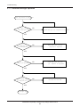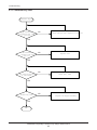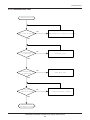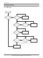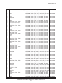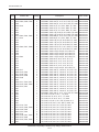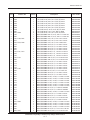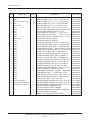
1
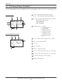
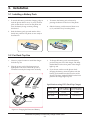
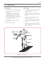
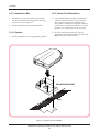
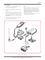
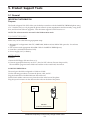
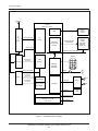
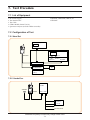
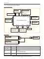
PORTABLE CELLULAR
TELEPHONE
SCH-3500 Series
SERVICE
PORTABLE CELLULAR TELEPHONE
Manual
CONTENTS
1. General Introduction
2. Specification
3. Installation
4. NAM Programming
5. Product Support Tools
6. Circuit Description
7. Test Procedure
8. Trouble Shooting
9. Exploded Views and Parts List
ABC
DEF
GHI
JKL
MNO
PQRS
TUV
WXYZ
SPACE
10. Block Diagram
11. Electrical Parts List
12. PCB Diagrams
13. Circuit Diagrams
1. General Introduction
The SCH-3500 DBDM(Dual Band Dual Mode) phone functions as both analog phone working in AMPS
(Advanced Mobile Phone Service) mode and digital phone working in PCS (Personal Communication Service)
mode.
The following standards and minimum performance standards shall be met or exceeded by each subscriber
unit.
Air Interface
The Subscriber Unit shall be Dual mode and Dual band in compliance with ANSI J-STD-008 and TIA/EIA IS95A(Analog).
ANSI J-STD-008 : Personal Station-Base Station Compatibility Requirements for 1.8 to 2.0 GHz CDMA PCS.
ANSI J-STD-018 : Recommended Minimum Performance Requirements for 1.8 to 2.0 GHz CDMA Personal
Stations.
CDG Ref. Document #27 : High Rate Speech Service Option for Wideband Spread Spectrum System.
TIA/EIA IS-96A : Speech Service Option 1 Standard for Dual mode Wideband Spread Spectrum Cellular
Systems.
TIA/EIA IS-125 : Recommended Minimum Performance standards for Digital Cellular Wideband Spread
Spectrum Speech Service Option1.
TIA/EIA IS-126-A : Mobile Station Loop back Service Option standard.
TIA/EIA IS-95A : Mobile Station-Base Station Compatibility Standard for Dual-Mode Wideband Spread
Spectrum Cellular Systems;for the analog air interface.
TIA/EIA IS-98A : Recommended Minimum Performance Requirements for 1.8 to 2.0 GHz CDMA Personal
Stations.
CDMA Receiver/Transmitter Specifications and Requirements
The Subscriber Unit shall comply with ANSI J-STD-008 and meet or exceed TIA/EIA IS-98A. The Subscriber
Unit shall comply with Personal Station Class II.
Analog Receiver/Transmitter Specifications and Requirements
The Subscriber Unit shall comply with TIA/EIA IS-95A and meet or exceed TIA/EIA IS-95. The Subscriber Unit
shall comply with Mobile Station Power Class III (600 mW).
SAMSUNG Proprietary-Contents may change without notice
1-1
2. Specification
2-1 General
Frequency Range
Transmitter
Receiver
PCS Mode
1850 ~ 1910 MHz
1930 ~ 1990 MHz
AMPS Mode
824 ~ 849 MHz
869 ~ 894 MHz
Channel Spacing
1.25 MHz
30 kHz
Number of Channels
1200
832
Duplex Spacing
80 MHz
45 MHz
Frequency Stability
(FRX - 80 MHz) ± 150 Hz
± 2.5 ppm
Operating Temperature
-30 C ~ 60 C
Operating Voltage
HHP
Hands-free
3.6V DC (± 10%)
13.7V DC (± 10%)
Size and Weight
Including standard battery
Including extended-life battery
11.2 x 5.2 x 2.5 cm, 146 cc, 146 g (5.1 ounces)
11.2 x 5.2 x 3.0 cm, 175 cc, 166 g (5.8 ounces)
o
o
SAMSUNG Proprietary-Contents may change without notice
2-1
Specification
2-2 AMPS Mode
TRANSMITTER
RF output power
: 0.6 W (+2/ - 4 dB)
Carrier ON/OFF Conditions
“ON” Condition
“OFF” Condition
: within ± 3 dB of specification output (in 2mS)
: below - 60 dBm (in 2mS)
Compressor
Compression Rate
Attack Time
Recovery Time
Reference Input
: 2:1
: 3 mS
: 13.5 mS
: Input level for producing a nominal ± 2.9 kHz peak
frequency deviation of transmitted carrier
Preamphasis
: 6 dB/OCT within 0.3 ~ 3 kHz
Maximum Frequency Deviation
F3 of G3
Supervisory Audio Tone
Signaling Tone
Wideband Data
: ± 12 kHz (± 10 %)
: ± 2 kHz (± 10 %)
: ± 8 kHz (± 10 %)
: ± 8kHz (± 10 %)
Post Deviation Limiter Filter
3.0 kHz ~ 5.9 kHz
5.9 kHz ~ 6.1 kHz
6.1 kHz ~ 15 kHz
Over 15 kHz
: above 40LOG (F/3000) dB
: above 35 dB
: above 40 LOG (F/3000) dB
: above 28 dB
Spectrum Noise Suppression
For All Modulation
f0 + 20 kHz ~ f0 + 45 kHz
: above 26 dB
For Modulation by Voice and SAT
f0 + 45 kHz
: above 63 + 10LOG (Py) dB
For Modulation by WBD (without SAT) and ST (with SAT)
f0 + 45 kHz ~ f0 + 60 kHz
: above 45 dB
f0 + 60 kHz ~ f0 + 90 kHz
: above 65 dB
f0 + 90 kHz ~ 2f0
: above 63 + 10LOG (Py) dB
(where f0 = carrier frequency,
Py = mean output power in watts)
Harmonic and Conducted Spurious Emissions
: above 43 + 10 LOG (Py) dB
SAMSUNG Proprietary-Contents may change without notice
2-2
Specification
RECEIVER
DE-Emphasis
: -6 dB/OCT within 0.3 ~ 3 kHz
Expander
Expansion Rate
Attack Time
Recovery Time
Reference Input
: 1:2
: within 3 mS
: within 13.5 mS
: Output level to a 1000 Hz tone from a carrier within ±
2.9 kHz peak frequency deviation
Sensitivity
: 12 dB SINAD/-116 dBm
Intermodulation Spurious Response Attenuation
: above 65 dB
RSSI Range
: above 60 dB
Protection Against Spurious Response Interference
: above 60 dB
In Band Conducted Spurious Emissions
Transmit Band
Receive Band
: below -60 dBm
: below -80 dBm
Out of Band Conducted Spurious Emissions
: below - 47 dBm
Radiated Spurious Emissions
Frequency Range
25 ~ 70 MHz
70 ~ 130 MHz
130 ~ 174 MHz
174 ~ 260 MHz
260 ~ 470 MHz
470 ~ 1 GHz
Maximum Allowable EIRP
-45
-41
-41
-32
-32
-21
dBm
dBm
~ -32 dBm
dBm
~ -26 dBm
dBm
SAMSUNG Proprietary-Contents may change without notice
2-3
Specification
2-3 PCS Mode
TRANSMITTER
Waveform Quality
: 0.944 or more
Open loop Power Control Range
-25 dBm
-65 dBm
-104 dBm
: -60.5 dBm ~ 41.5 dBm
: -20.5 dBm ~ -1.5 dBm
: +15.0 dBm ~ +30.0 dBm
Minimum Tx Power Control
: -50 dBm below
Closed Loop Power Control Range
: ±24 dB
Maximum RF Output Power
: 200 mW (+23 dBm)
Occupied Bandwidth
: 1.23 MHz
Conducted Spurious Emissions @ 1.25 MHz
: -42 dBc/30 KHz
RECEIVER
Rx Sensitivity and Dynamic Range
(Rate Set 2)
: -104 dBm, FER=0.5% or less
: -25 dBm, FER=0.5% or less
Conducted Spurious Emission
1930 ~ 1990 MHz
1850 ~ 1910 MHz
All Other Frequencies
: <-81 dBm
: <-61 dBm
: <-47 dBm
Single Tone Desensitization
Rx power = -101 dBm
Tx power = +15 dBm(According to IS-98C)
Tone power = -30 dBm
Tone offset from carrier = ±1.25 MHz
: lower than 1%
Intermodulation Spurious Response Attenuation
Rx power = -101 dBm
Tone power 1 = -43 dBm
Tone power 2 = -43 dBm
Tone 1 offset from carrier = ±1.25 MHz
Tone 2 offset from carrier = ±2.05 MHz
: lower than 1%
SAMSUNG Proprietary-Contents may change without notice
2-4
Specification
2-4 PCS Debug Display Information
To select debug display mode : Press [MENU] + [9] + [0], and press [0] + [4] + [0] + [7] + [9] + [3], and press [1].
1 Sxxxxx : SID (System Identification) toggle
Nxxxxx : NID (Network Identification) toggle
IN IDLE MODE
1
4
7
2
3
Sxxxxx SIx
x
T - xx
Dxxx - xx
Pxxx
CHxxxx
xx xx
12
6
8
3 Handset Status : 0 - NO SVC
1 - Synchronization
2 - Paging (Idle)
3 - Reg. Access state
4 - Traffic Initialization
5 - Waiting for order
6 - Waiting for answer
7 - Conversation state
8 - Exit
5
IN CONVERSATION MODE
9
10
2 SIx : Slot cycle index (lowest between the system
and the phone will be used)
1. SI0 : Slot Index 0
2. SI1 : Slot Index 1
3. SI2 : Slot Index 2
11
4 T-xx : Tx adjust, Value ranges from -63~+63dB
TVx RVx xx x
T - xx
Dxxx - xx
Pxxx
CHxxxx
xx xx
3
5 Dxxx : Sector power in dBm
6 -xx : ec/lo
7 Pxxx : PN offset
12
8 CHxxxx : Channel number
9 TV : Tx vocoder rate (8 is full rate, 1 is 1/8th rate)
10 RV : Rx vocoder rate (8 is full rate, 1 is 1/8th rate)
11 xx : Walsh code used in traffic channel
12 System acquisition state
SAMSUNG Proprietary-Contents may change without notice
2-5
Specification
2-5 AMPS Debug Display Information
To select debug display mode : Press [MENU] + [9] + [0], and press [0] + [4] + [0] + [7] + [9] + [3], and press [1].
1 SIDxxxxx : AMPS Home System ID
1
7
4
2 PWRx : Power Level 0 ~ 7
3 SATx : Supervisory Audio Tone code (0 ~ 2)
2
3
SIDxxxxx
x
x
PWRx
RSSIxxx
SATx
CHxxxx
xx xx
5
4 x (Using Frequency Band) : A Band or B Band
5 RSSIxxx : RSSI value
6 CHxxx : Channel number
8
6
7 Handset Status : 1 - Initialization state
2 - Idle state
3 - System Access state
4 - Voice channel state
8 System acquisition state
SAMSUNG Proprietary-Contents may change without notice
2-6
3. Installation
3-1 Installing a Battery Pack
1.
2.
To attach the battery pack after charging, align it
with the phone about 1cm (1/2”) away from its
place so that the two arrows on the phone are
seen, the battery charge contacts pointing
downward.
3.
To remove the battery pack, release it by
pressing the button on the rear of the phone.
4.
Slide the battery pack downward about 1cm
(1/2”) and lift it away from the phone.
Slide the battery pack upwards until it clicks
firmly into position. The phone is now ready to
be turned on.
Press this button to
release the battery pack.
3-2 For Desk Top Use
1.
Choose a proper location to install the charger
for desk top use.
2.
Plug the power cord of the charger into an
appropriate wall socket. When the power is
connected correctly, the lamps turn on briefly.
3.
To charge the battery pack, insert the battery
pack into the rear slot of the charger. The lamp
marked BATT on the front panel of the charger
lights up red.
4.
If you do not wish to use the phone while
charging the battery, insert the phone with the
battery pack attached into the front slot of the
charger. The lamp marked PHONE on the front
panel of the charger lights up red.
Specifications using DTC (Desk Top Charger)
SCH-3500 MAIN
STANDARD
BATTERY
PACK (BTS350)
EXTENDED
BATTERY PACK
(BTE350)
Battery Type
Standard Battery Extended battery
(Li-ion, 1000mAh)
Charging Time
SEC Code
(Li-ion, 1600mAh)
3 hours
4 hours
GH43-10316B
GH43-00121A
DTC : DTC350
Figure 3-1 Charging the Phone and Battery
SAMSUNG Proprietary-Contents may change without notice
3-1
Installation
3-3 For Mobile Mount
3-3-1 Antenna
3-3-2 Cradle
1.
1.
Choose a location where it is easy to reach and
does not interfere with the driver’s safe
operation of the car.
2.
Separate the two halves of the clamshell by
removing the two large slotted screws. See the
figure 3-2.
3.
Drill holes and mount the lower half of the
clamshell by using the screws.
4.
Place the cradle onto the remaining half of the
clamshell and assemble them by using the
screws.
5.
Reassemble the two halves of the clamshell
together. Adjust the mounting angle and tighten
the two slotted screws.
Choose a proper location to install the antenna.
•The center of the roof top provides the best
performance.
•The edge of the rear trunk also provides a
good performance. However, the antenna
should be higher than the roof of the car.
•In case of on-glass antenna, you should align
the antenna base with the round plate to
connect the cables correctly.
2.
Mount the antenna vertically, connect the
antenna cable.
3.
Tighten the antenna nut fully.
SCH-3500
MAIN PHONE ANTENNA
CRADLE
CLAM SHELL
MOUNT UPPER
HANDS
FREE BOX
FIXED SCREW
CLAM SHELL
MOUNT LOWER
CAR
32
32
Figure 3-2 Cradle Installation
SAMSUNG Proprietary-Contents may change without notice
3-2
Installation
3-3-3 Hands-Free Box
3-3-5 Hands-Free Microphone
1.
Drill holes in a proper location for the handsfree box, attach the mounting bracket by using
the screws. See the figure 3-3.
1.
2.
Install the hands-free box into the bracket.
It is recommended to install the microphone
where it is 30-45 cm (12-18”) away from the
driver. Choose the location where is least
susceptible to interference caused by external
noise sources, ie, adjacent windows, car audio
speakers, etc. Normal place is the sun visor.
2.
Once the microphone has been correctly
positioned, connect the microphone wire to the
MIC jack on the hands-free box.
3-3-4 Speaker
1.
Install the speaker into the appropriate position.
MOUNTING BRACKET
CAR
40
55
Figure 3-3 Hands-Free Box Installation
SAMSUNG Proprietary-Contents may change without notice
3-3
Installation
3-3-6 Cables
1.
Connect the cradle and the hands-free box with
the data cable. See the figure 3-4.
2.
Connect the antenna cable to the RF jack of the
cradle.
3.
Connect the red wire to the battery (+) terminal,
black wire to the vehicle chassis, brown wire to
the Car Audio Mute port and orange wire to the
ignition port in the key box of vehicle or battery
(+) terminal.
4.
Connect the other end of the power cable to the
PWR jack of the hands-free box.
Notes:
•It is recommended to connect the power cable
directly to the battery to avoid power noise.
•Make sure the connection between the battery (-)
terminal and vehicle chassis is made correctly.
•Make sure the fuse having a proper capacity is
used on the power cable.
•Make sure the cables do not pass over any sharp
metal edge that may damage it.
Red
Black
Brown
Orange
Figure 3-4 Cable Connections
SAMSUNG Proprietary-Contents may change without notice
3-4
4. NAM Programming
NAM features can be programmed as follows:
Notes:
- If you enter the NAM program mode, each item shows the currently stored data. Go to the next item by
pressing OK.
- You can modify the data by entering a new data.
- If you enter a wrong digit, press CLR to delete the last digit. Press and hold CLR to delete all digit.
- To scroll items backwards press the VOLUME button on the left side of the phone.
4-1 Single NAM
4-1-1 General Setup
LCD Display
Key in
Function
Menu, 6, 0
Select NAM programming
6-digit code
Enter random 6 digit code (MSL)
2
Choose ‘General’
Volume „
Electronic Serial Number of the phone is displayed
CAI version
1
Volume „
Common Air Interface version is displayed
VOC8/13/EVRC
SO_VOICE_13K
Volume „
SCM
Volume „
Enter Lock
??????
SVC Menui
1:Phone#
2:General
3:NAM
m
ESN
B0000000
10101010
Lock Code
0000
Slot Mode
Yes
4-digit code
OK
Lock code, current status is displayed.
-to change, enter new code.
-stores it.
ˆ or ¤
OK
Slot mode. ‘Yes’ indicates the slot mode.
-changes the status.
-store it.
0~7
OK
Slot mode index. The higher, the longer sleeping time.
-to change, enter new one.
-stores it.
Slot Index
2
Station Class Mark displays the power class, transmission,
slotted class, dual mode.
SAMSUNG Proprietary-Contents may change without notice
4-1
NAM Programming
4-1-2 Phone #
LCD Display
SVC Menui
1:Phone#
2:General
3:NAM
m
Phone #
1234567890
Mobile ID #
1234567890
Key in
Function
Choose ‘Phone#’.
1
Phone number
OK
Mobile ID
OK
4-1-3 Setting Up NAM
LCD Display
SVC Menui
1:Phone#
2:General
3:NAM
m
IMSI_MCC
310
Key in
3
Choose ‘NAM’.
Number
OK
IMSI Mobile Country Code, current code is displayed.
-to change, enter new one.
-stores it.
Number
OK
IMSI Mobile Network Code, current code is displayed.
-to change, enter new one.
-stores it.
Class number
OK
CDMA Access Overload Class, current status is displayed.
-to change, enter new one.
-stores it.
ˆ or ¤
OK
CDMA Home system ID, current status is displayed
-change the status
-store it.
IMSI_MNC
00
CDMA ACCOLC
0
CDMA HomeSID
Yes
Function
SAMSUNG Proprietary-Contents may change without notice
4-2
NAM Programming
LCD Display
Key in
Function
Yes
ˆ or ¤
OK
CDMA foreign SID, current status is displayed.
-change the system.
-store it.
Yes
ˆ or ¤
OK
CDMA foreign NID, current status is displayed.
-change the system
-store it.
HOME SID
4120
Number
OK
SID written in the list, current status is displayed.
-to change, enter new one.
-store it.
NID
Number
OK
NID written in the list, current status is displayed.
-to change, enter new one.
-store it.
CDMA fSID
CDMA fNID
65535
SAMSUNG Proprietary-Contents may change without notice
4-3
5. Product Support Tools
5-1 General
IMPORTANT INFORMATION
Purpose
The Product Support Tool (PST) offers you the ability to interface with the SAMSUNG DBDM telephone using
a PC. With this tool you can program the phones network system requirements and functionality, swap phone
data, and download software upgrades. This document supports UniPST version x.xx.
NOTE: This software must be executed in the Windows95/98 mode.
EQUIPMENT REQUIRED
Make sure you have the following equipment setup:
1. Minimum PC configuration: 586 CPU, 16MB RAM, Windows95/98, 5MB of disk space free for software
upgrade.
2. PST Software with appropriate cable (DM Cable for SAMSUNG DBDM phone).
3. Serial Port (16550 Serial Interface Card).
4. Power Supply (3.8 V) or Battery.
INSTALLATION
Software
1.Insert the PST floppy disk into drive (A:\).
2.Create an appropriate directory on the C:\ drive for PST software, Execute Setup.exe file,
The installation program creates folder and task bar on the windows95/98 start bar.
SAMSUNG DBDM Phone
The serial port should be configured to COM1 or COM2.
Use the following procedure to connect the phone, cable, and PC .
Plug the female end of the DM Cable into the 16550 card.
Pull the black rubber connector away from the socket at the base of the phone.
Plug the special connector on the cable into the socket at the base of the phone.
PC
Phone
DB Cable
(Parts No.:GH39-30525A)
SAMSUNG Proprietary-Contents may change without notice
5-1
Product Support Tools
5-2. PST (Product Support Tool)
5-2-1 Getting Started
MAIN MENU SCREEN
1. At the Windows95/98, Double Click “UniPst.exe”.
2. The Main Menu Screen will be displayed.
The Main Menu Screen shows the basic tasks that are available.
CAUTION: DO NOT attempt to program phone with a low battery.
PST SETUP
UniPst supports SAMSUNG DBDM portable telephone. You can select serial port COM1 or COM2.
5-2-2 Operation Procedure
Service Programming
The Service Programming screens enable you to set and change the service activation parameters of the
phones. These items can be changed individually or as a group via the “Edit Items” Property Sheet of the PST.
There are several pages on the Service Programming Property Sheet (See below Figure).
Read Data from File
Click “open” icon to select the name of a file whose extension is “mmc”. The values will be read from the
named file, and will initialize the parameter values seen on the Service programming screen
Read Data from Phone
Click Read from the Phone icon to upload the current programmable parameters of the phone. The values are
read from the phone, so the phone must have the power ON and be properly connected to the PST.
NOTE: To actually view the data you need to go to the Edit Items screens.
Edit Items
Click this icon to edit Number Assignment Module (NAM) items or UI items.
There are two types of screens:
1. Parameters associated with a particular Number Assignment Module (NAM)
2. UI items settings
Phone Book
Click this icon to edit Phone Book.
While you edit cell, you can use <Enter> and < UP , DOWN,LEFT,LIGHT Arrow> and <SPACE> key. If you
want to edit phone number or name , you must move rectangle box to cell where you want to edit , Write it
down . if <UP and DOWN Arrow> key is pressed, the cursor moves to next cell or previous cell.
SAMSUNG Proprietary-Contents may change without notice
5-2
Product Support Tools
Save Data to File
Click this icon to save the current parameters to a file. Once you enter a filename, Click <OK> button to write
all current parameters to that file. This way the same information can be downloaded into multiple phones.
Write to Phone
Click this icon to write the selected parameter values to the phone. Writing the selected values to the phone
may take up to a minute.
If there are dependencies in a field you can make all the changes in the proper fields and download the
information all together.
If you intend to use this “Write to Phone” feature, it is recommended that you do a “Read Data from Phone”
first, and then make the changes, so that nothing gets inadvertently overwritten.
NOTE: DO NOT TOUCH THE PHONE WHILE WRITING IS IN PROGRESS.
Software Download and Upgrade Screen
To begin a software upgrade or download, perform the following steps:
1. From the main menu screen choose DOWNLOAD MODE?
Click open icon to choose a BIN file of the new software to be loaded. Choose the appropriate BIN file, then
Click <Open> (see below figure).
2. Click Download? to begin downloading the file. You will notice various messages and a progress bar that
informs the user what percentage of the downloading has already occurred.
3. Click Mode Select box, then Select SERVICE MODE?to return to the Service Mode Screen.
NOTE: DO NOT POWER OFF WHILE THE PHONE IS BEING DOWNLOADED!
SAMSUNG Proprietary-Contents may change without notice
5-3
6. Circuit Description
6-1 Logic Section
6-1-1 Power Supply
CPU
With the battery installed on the phone and by
pressing the PWR key, the VBATT and ON_SW
signals will be connected. This will turn on Q905
(2SC4081BR). This in turn will be supplied to
regulators (U905 and U907), thus releasing them
from the shut-down state to output regulated 3.0V.
The VBATT applied to ON_SW will turn on Q907
(DTC144EE) resulting in the signal ON_SW_SENSE
to change state from HIGH to LOW. This will allow
MSM to send out PS_HOLD (logical HIGH) to turn
on Q905 even after the PWR key is released.
The voltage (+3.0VD) from U907 is used in the
digital parts of MSM. The voltage (+3.0VA) from
U905 is used in the analog part.
ARM7TDMI microprocessor is used for the main
processing. The CPU controls all the circuitry. For
the CPU clock, 27 MHz resonator is used.
MEMORY (U801)
16M Flash and 4 M SRAM one package is used to
store the terminals programs , the internal flag
information, call processing data, and timer data.
Using the down-loading program, the program can
be changed even after the terminal is fully
assembled.
EEPROM (U903)
One 256 kbit EEPROM is used to store ESN, NAM,
power level, volume level, and telephone number.
6-1-2 Logic Part
The Logic part consists of internal CPU of MSM,
Memory and EEPROM. The MSM receives TCXO
and CHIPX8 clock signals from the IFR and controls
the phone during the CDMA and the FM mode. The
major components are as follows:
•CPU
: ARM7TDMI Micro-processor
•Memory
: U801 (MB84VD21194-85-PBS)
16M Flash ROM, 4M SRAM
•EEPROM
: U903 (M24256)
256K Serial EEPROM
KEYPAD
For key recognition, key matrix is setup using
SCAN0-6 of STORE signals and KEY0-3 of input
ports of MSM. Ten LEDs and backlight circuitry are
included in the keypad for easy operation in the
dark.
LCD MODULE
LCD module contains a controller which will
display the information onto the LCD by 8-bit data
from the MSM.
SAMSUNG Proprietary-Contents may change without notice
6-1
Circuit Description
6-1-3 Baseband Part
MOBILE SYSTEM MODEM (MSM)
ADC Interface
The MSM equipped with the ARM7TDMI core is an
important component of the CDMA cellular phone.
The MSM comes in a 196 pins BGA package. The
interface block diagram is shown on page 6-3.
ADC_CLK (pin C1), ADC_ENABLE (pin C2) and
ADC_DATA (pin B1) are required to control the
internal ADC in the IFT/IFR.
Data Port Interface
MICROPROCESSOR INTERFACE
The interface circuitry consists of reset circuit,
address bus (A0-A19), data bus (AD0-AD15), and
memory controls (ALE, DT_R, HWR/, LWR/,
ROM_CS).
INPUT CLOCK
•CPU clock: 27 MHz
•TXCO(pin L2): 4.92 MHz. This clock signal from
the IFR is the reference clock for the MSM except
in CDMA mode.
•CHIPX8(pin H2) : 9.8304 MHz. The reference clock
used during the CDMA mode.
•SLEEP-XTAL-IN/OUT(pins M10, P12) : 32.768
kHz
IFT/IFR INTERFACE
CDMA, FM Data Interface
•TXIQDATA0-7 (pins L1, J3, K2, K1, J4, H3, J1, J2) :
TX data bus used during both CDMA and FM
mode.
•C_RX_IDATA0-3 (pins G1-G4) and
C_RX_QDATA0-3 (pins F1-F4) : RX data bus used
during CDMA mode.
•FM_RX_IDATA (pin E4) and FM_RX_QDATA (pin
E3) : RX data bus used during FM mode.
Clock
•TX_CLK (pin H1), TX_CLK/(pin H4) : Analog to
Digital Converter (ADC) reference clock used in
TX mode.
•CHIPX8 : ADC reference clock used in CDMA RX
mode.
•FMCLK : Reference clock in FM RX mode.
Includes the UART. Also, supports Diagnostic
Monitor (DM) and HP equipment interface.
CODEC Interface
The MSM outputs 2.048 MHz PCM_CLK (pin B11)
and 8 kHz PCM_SYNC (pin C11) to the CODEC
(U902). The voice PCM data from the MSM (U908)
PCM_DIN (pin A12) is compressed into 8 kHz by
QCELP algorithm in the CDMA mode. In FM mode,
the data is processed by D_FM.
RF Interface
TX : TX_AGC_ADJ (pin K3) port is used to control
the TX power level and PA_ON (pin L4) signal is
used to control the power amplifier.
RX : RX_AGC_ADJ (pin M1) port is used to control
the RX gain and TRK_LO_ADJ (pin N3) is used to
compensate the TCXO clock.
General Purpose I/O Register Pins
Input/output ports to control external devices.
Power Down Control
When the IDLE/ signal turns LOW, only the TX
sections will be disabled. If both the IDLE/ and
SLEEP/ changes to LOW, all the pins except for the
TXCO is disabled.
SAMSUNG Proprietary-Contents may change without notice
6-2
Circuit Description
ANTENNA
MSM3000
Mobile Station Modem
External
Test/Debug
System
UART
RF
and
IF
Circuits
RF Control Signals
RF
Interface
Peripheral
Circuits
(RAM, ROM,
EEPROM,
Display, etc.)
Microprocessor Bus
Address/Data
ARM7TDMI
Microprocessor
Subsystem
Offset Controls
General-Purpose Interface Bus
Keypad
Receive Data
and Status
IFR3000
1 2 3
4 5 6
7 8 9
0
CDMA
Processor
GENERAL
PURPOSE
INTERFACE
Transmit I and Q Data
IFT3000
RINGER
Receive Data
and Status
Receive Data
and Status
DFM
PROCESSING
SPK
PCM Data
General Purpose
ADC Interface
CODEC
MIC
VOCODER
PCM Data
MODE Select Interface
ANSI/IEEE 1149.1-1990
JTAG Interface
Extemal Mode Selection
Digital Test Bus
Figure 6-1 Baseband Block Diagram
SAMSUNG Proprietary-Contents may change without notice
6-3
Aux.
CODEC
Circuit Description
6-1-4 Audio Part
RX AUDIO PATH
TX AUDIO PATH
De-Emphasis Circuit
The voice signal output from microphone is filtered
and amplified by the internal OP-AMP and is
converted to PCM data by the CODEC (U902). This
signal is then applied to the MSM (U908)'s internal
vocoder.
RX AUDIO PATH
The PCM data out from the MSM is converted to
audio signal by ADC of CODEC (U902), is then
amplified by CODEC (U902) to be sent to the
speaker unit.
This circuit is 1st LPF featuring -6dB/oct to reduce
signal loss and noise in Rx path.
Expander
The expander features 1:2 level to reduce signal loss
and noise in Rx path. The zero crossing level of the
expander is ±2.9 kHz/dev, attack time is 3 mS, and
release time is 13.5 mS.
Volume Adjust
Volume can be adjusted up to 6 steps for the user to
obtain a proper loudness of received signal.
FM TX PATH
Pre-Emphasis Circuit
6-1-5 TX WBD, ST, And SAT
The circuit features +6dB/oct to reduce signal loss
and noise in Tx path.
These signals are generated from MSM. The
modulation level of TX WBD and ST is
±8 kHz/dev, and SAT is ±2 kHz/dev.
Compressor
The compressor features 2:1 level to reduce signal
loss and noise in Tx path. The zero crossing level of
the compressor is ±2.9 kHz/dev, attack time is 3 mS,
and release time is 13.5 mS.
Limiter
6-1-6 Buzzer Driving Circuitry
Buzzer generates alert tone. When the buzzer
receives the timer signal from the MSM, it generates
alert tone. The buzzer level is adjusted by the alert
signal's period generated from the MSM timer.
The limiter performs to cut ±0.53 Vp-p or higher
audio signal level so that the FM frequency
deviation is not over ±12 kHz/dev. The function is
used to avoid confusion over phone line. LPF is
used to reduce a specific high frequency of limited
signal.
SAMSUNG Proprietary-Contents may change without notice
6-4
Circuit Description
6-2 Receiver (For PCS)
LOW NOISE AMPLIFIER (LNA)
VOLTAGE CONTROLLED OSCILLATOR
The low noise amplifier featuring 1.6 dB Noise
Figure and 20dB gain amplifier a weak signal
receiver from the base station to obtain the
optimum signal level.
The VCO (U201) generates the signal having
1750 MHz center frequency and ±30 MHz deviation
with voltage control. PLL IC (U204) controls this
signal.
DOWN CONVERTER (MIXER)
PHASE LOCKED LOOP (PLL)
First local signal is applied to this down converter.
The down converter transfers the signal amplified
at the LNA into 210.38 MHz IF signal. 210.38 MHz
IF signal is made by subtracting 1960 ±30 MHz RF
signal from 1750 ± 30 MHz first local signal. The
LAN is Q101 and down converter is U101.
LOCAL BUFFER AMPLIFIER
Buffer (Q203) amplifies signal to be applied to the
local input of the down converter (U101) when a
phase is locked between U201 and U204.
Input reference frequency is generated at VCTCXO
(U205) and the divider signal is generated at VCO.
PLL compares the two signals and generates the
desired signal with a preprogrammed counter
which controls voltage.
VOLTAGE CONTROLLED TEMPERATURE
COMPENSATED CRYSTAL OSCILLATOR
It provides 19.68 MHz reference frequency to PLL
(U204) and IFT (U501), IFR (U103). A correct
frequency tuning is made by the voltage control.
RF BAND PASS FILTER (BPF)
TEMPERATURE TO VOLTAGE CONVERTER
The RF BPF (F104) passes only a specific frequency
(1960±30MHz) from the signal received from the
mobile station. The band width is 60MHz.
The Temperature to Voltage Converter (U341)
detects temperature. It is used to compensate active
component characteristics due to the temperature
difference.
IF SAW BAND PASS FILTER
IF SAW BPF (F106) is used for CDMA system
having 1.23MHz wide band and ±630 kHz
bandwidth. The filter also climinates spurious
signals generated at the mixer.
DUPLEXER
Duplexer (F101) controls to transmit through the
antenna only the signals within acceptable Tx
frequency range (1880 ±30 MHz). It also matches
LNA (U401) input in receiving part and PA out in
transmitter part with the antenna.
SAMSUNG Proprietary-Contents may change without notice
6-5
Circuit Description
IFT3000 FEATURES
IFR3000 FEATURES
- Dual-mode operation for CDMA and AMPS
- 8-bit DACs convert digital baseband to analog
baseband
- CDMA and FM signal paths include low-pass
filrers for I and Q output waveform smoothing
- IF mixer up-converts analog baseband to IF
- Controls Tx power level with AGC amplfier
having 84 dB dynamic range
- Programmable Tx PLL for generating Tx IF
frequency
- VCO for generation of transmit LO mixing signal
- 8-bit general-purpose ADC with 3-input analog
multiplexer
- Operational modes compatible with MSM2300 and
MSM3000
- Three-line Serial Bus Interface (SBI) for control of
the IFT3000 via the MSM3000
- 48-lead TQFP packaging for dense mechanical
assemblies
- Dual-mode operation for CDMA and AMPS
- Rx power level with 90 dB dynamic analog
baseband
- IF mixer down-converts Rx IF to quadrature
analog baseband
- CDMA and FM signal paths include low-pass
filrers for accurate selection of I and Q baseband
components
- 4-bit ADCs convert CDMA I and Q analog
baseband signals to digital baseband data
- 8-bit ADCs convert FM I and Q analog baseband
signals to digital baseband data
- RX Slotting operation for very low power
consumption in CDMA and FM signal paths
- Clock generators for CDMA and AMPS operation
- VCO for generation of receive LO mixing signal
- I and Q offset control inputs drive baseband DC
offsets to zero in CDMA and FM signal paths
- Operational modes compatible with MSM2300 and
MSM3000
- Three-line Serial Bus Interface for initializing and
control of the IFR3000 from the MSM3000
- 48-lead TQFP (JEDEC Pub 95 MS-026 BBC)
packaging for dense circuit boards
SAMSUNG Proprietary-Contents may change without notice
6-6
Circuit Description
6-3 Receiver (For AMPS)
LOW NOISE AMPLIFIER (LNA)
VOLTAGE CONTROLLED OSCILLATOR
The low noise amplifier featuring 1.6 dB Noise
Figure and 20 dB gain amplifier a weak signal
receiver from the base station to obtain the
optimum signal level.
The VCO (U202) generates the signal having
966MHz center frequency and ±12.5 MHz deviation
with voltage control. PLL IC (U204) controls this
signal.
DOWN CONVERTER (MIXER)
PHASE LOCKED LOOP (PLL)
First local signal is applied to this down converter.
The down converter transfers the signal amplified
at the LNA into 85.38 MHz IF signal. 85.38 MHz IF
signal is made by subtracting 881 ±12.5 MHz RF
signal from 966 ± 12.5 MHz first local signal. The
LNA is Q102 and down converter is U102.
Input reference frequency is generated at VCTCXO
(U205) and the divider signal is generated at VCO.
PLL compares the two signals and generates the
desired signal with a preprogrammed counter
which controls voltage.
LOCAL BUFFER AMPLIFIER
VOLTAGE CONTROLLED TEMPERATURE
COMPENSATED CRYSTAL ASCILLATOR
Buffer (Q204) amplifies signal to be applied to the
local input of the down converter (U412) when a
phase is locked between U202 and U204.
It provides 19.68 MHz reference frequency to PLL
(U204) and IFR (U103), IFT(U501). A correct
frequency tuning is made by the voltage control.
RF BAND PASS FILTER (BPF)
DUPLEXER
The RF BPF (F105) passes only a specific frequency
(881.49±12.5MHz) from the signal received from the
mobile station. The band width is 25 MHz.
Duplexer (F103) controls to transmit through the
antenna only the signals within acceptable Tx
frequency range (836 ±12.5 MHz). It also matches
LNA (Q102) input in receiving part and PA out in
transmitter part with the antenna.
IF SAW BAND PASS FILTER
IF SAW BPF (F107) is used for AMPS system having
30kHz channel spacing and ±15 kHz bandwidth.
The filter also climinates the spurious signals at the
mixer.
SAMSUNG Proprietary-Contents may change without notice
6-7
Circuit Description
6-4 Transmitter Section (For PCS)
POWER AMP
RF BAND PASS FILTER (BPF)
Power Amp module (U412) amplifier signal to be
sent out to the base station through the antenna.
The RF BPF (F403, F404) accepts only specific
frequency (1880±30 MHz) to send it out to power
and Power Amp module. The band width is 60
MHz.
DRIVER AMP
The driver amp (U409) allows the signal input to
the Power Amp module (U412) to be within a
specified level.
ISOLATOR
Isolator (U413) is used to reduce a reflected signal to
protect the power amp module from being
damaged.
UP CONVERTER (MIXER)
The up converter (U406) receives the first local
signal to generate 1880±30 MHz. 1880 ±30 MHz
signal comes out from the mixer output by adding
130MHz IF signal to 1750±30 MHz first local signal.
Up converter’s reference number is U406.
POWER SUPPLY REGULATOR
The power supply regulator (U344) supplies a
regulated power to each part of transmitter. VBatt is
connected to power Amp Module (U412) directly.
U344 supplies 3.0 V to the others.
ANTENNA
Antenna allows signal to send to receive from the
base station.
6-5 Transmitter Section (For AMPS)
POWER AMP MODULE
RF BAND PASS FILTER (BPF)
Power Amp module (U411) amplifier signal to be
sent out to the base station through the antenna.
The RF BPF (F402, F405) accepts only specific
frequency (836±12.5 MHz) to send it out to base
station module. The band width is 25 MHz.
UP CONVERTER (MIXER)
POWER SUPPLY REGULATOR
The up converter (U407) receives the first local
signal to generate 836±12.5 MHz. 836 ±12.5 MHz
signal comes out from the mixer output by adding
130MHz IF signal to 966±12.5 MHz first local signal.
The power supply regulator (U343) supply a
regulated power to each part of transmitter. U343
supplies 3.0V to TX driver (U408), mixer (U407) and
VBatt is connected to Power Amp Module (U411)
directly.
ANTENNA
Antenna allows signal to send to receive from the
base station.
SAMSUNG Proprietary-Contents may change without notice
6-8
Circuit Description
6-6 Test Command Table
To change the phone from normal mode to test mode, you should enter the following keys. :
Press [4 7 * 8 6 9 # 1 2 3 5]
Command No.
(OP, AB, RB)
Command SW Name
01(1F, 0, 0)
T_SUSPEND_I
Terminate the normal mode, enter to the test mode.
02(3f, 0, 0)
T_RESTART_I
Terminate the test mode, enter to the normal mode.
03(FD, 0, 0)
T_SAVE_VAL_I
Save value in EEPROM. (Only for Auto test)
04(1D, 0, 1)
T_GET_MODE_I
Get mode. (CDMA or AMPS)
05(1C, 1, 0)
T_SET_MODE I
Set mode to CDMA or AMPS. (Only for Auto test)
06(1E, 0, 0)
T_WRITE_NV_I
Write an EEPROM item. (one of the NV items)
07(81, 0, 0)
T_CARRIERON_I
Turn the carrier on.
08(82, 0, 0)
T_CARRIEROFF_I
Turn the carrier off.
09(83, 4, 0)
T_LOADSYN_I2)
Set the synthesizer to the channel specified by ch_ data.
10(84, 1, 0)
T_PWRLEVEL_I
Set the RF power attenuation to the specified value.
11(85, 0, 0)
T_RXMUTE_I
Mute the receive-audio signal.
12(86, 0, 0)
T_RXUNMUTE_I
Unmute the receive-audio signal.
13(87, 0, 0)
T_TXMUTE_I
Mute the transmit-audio signal.
14(88, 0, 0)
T_TXUNMUTE_I
Unmute the transmit-audio signal.
16(8F, 0, 0)
T_STON_I
Transmit a continuous Signaling Tone (ST).
17(90, 0, 0)
T_STOFF_I
Stop transmit a continuous Signaling Tone (ST).
20(94, 4, 0)
T_TEST_SYS_I
2)
Description
Roam Test System
1)
22(91,96,96)
T_SNDNAM_I
Display and send NAM information.
23(95, 3, 4)
T_SNDVERSION_I
24(9F, 7, 8)
T_SNDESN_I
Display and return ESN.
25(92, 0, 0)
T_BACKLIGHT_ON_I
Turn on the backlight.
26(93, 0, 0)
T_BACKLIGHT_OFF_I
Turn off the backlight.
27(96, 0, 0)
T_LAMP_ON_I
Turn on the LAMP.
28(97, 0, 0)
T_LAMP_OFF_I
Turn off the LAMP.
30(9D,16, 0)
T_PLINE_I
Display and return production date.
1)
1)
2)
Display and return S/W version.
32(A0, 1, 0)
T_SATON_I*
Enable the transmission of SAT.
33(A1, 0, 0)
T_SATOFF_I*
Disable the transmission of SAT.
34(A2, 0, 0)
T_CDATA_I
Transmit continuous 5-word Reverse CTL CH message.
35(A3, 0, 0)
T_VOLUME_UP_I
Increase value of the last command. (Only for autotest)
36(A4, 0, 0)
T_VOLUME_DOWN_I
Decrease value of the last command. (Only for autotest)
42(AA, 1, 0)
T_DTMFON_I
2)
Activate DTMF generator with keycode.
SAMSUNG Proprietary-Contents may change without notice
6-9
Circuit Description
Command No.
(OP, AB, RB)
Signal. Name
Description
43(AB, 0, 0)
T_DTMFOFF_I
Deactivate DTMF generator.
44(B0, 0, 0)
T_COMPANDORON_I
Enable the compressor and expandor.
45(B1, 0, 0)
T_COMPANDOROFF_I
Disable the compressor and expandor.
46(B2, 0, 0)
T_AMPS_VCLINE_I*
Enter Analog voice channel state.
47(B3, 3, 0)
T_AMPS_AUD_GAIN_I
FM audio gain.
48(B4, 0, 0)
T_VIBRATOR_ON_I
Activate a vibrator.
49(B5, 0, 0)
T_VIBRATOR_OFF_I
Deactivate a vibrator.
50(B6, 0, 4)
T_BATT_TYPE_I
Battery type.
51(B7, 1, 1)
T_BBA_I
BASIC supplier
52(B9, 2, 2)
T_HW_VERSION_I
HW version
57(BC, 0, 0)
T_MIC_ON_I
Mic path on.
58(BD, 0, 0)
T_MIC_OFF_I
Mic path off.
59(BE, 0, 0)
T_ALLPATH_I
Set RX Path, TX path Unmute to Earpiece.
60(BF, 3, 0)
T_AMPS_TX_GAIN_I
61(C0, 3, 0)
T_AMPS_RX_GAIN_I
62(C1, 3, 0)
T_DTMF_VOL_TX_I
63(C2, 3, 0)
T_TX_LIMITER_I
2)3)
AMPS TX Audio Gain Control.
2)3)
AMPS RX Audio Gain Control.
2)3)
AMPS TX DTMF Gain Control.
2)3)
AMPS TX Limiter Gain Control.
2)3)
64(C3, 3, 0)
T_AMPS_SAT_LEVEL_I
AMPS TX SAT level Control.
65(C4, 3, 0)
T_AMPS_FREQ_SGAIN_I
66(C5, 3, 0)
T_AMPS_ST_GAIN_I
67(C6, 3, 6)
T_READ_BATT_I
68(C8, 0, 3)
T_VBATT1_I
69(C9, 0, 3)
T_VBATT2_I
70(CA, 3, 0)
T_WRITE_BATT_I
71(D1, 3, 0)
T_CDMA_TXADJ_I
2)3)
2)3)
1)
AMPS TX Master Gain Control.
AMPS TX ST Gain Control.
Read low batt in the standby, talk mode.
3)
Set the low battery position in the standby.
3)
Set the low battery position in the talking.
3)3)
2)
2)
72(D2, 3, 0)
T_AMPS_TXADJ_I
73(D3, 1, 0)
T_SET_PA_R_I
74(D4, 4, 0)
T_TXRAS_ADJ_I
75(D5, 0, 3)
T_READ_RSSI_I
76(D5, 3, 0)
T_WRITE_RSSI_I
2)
Write low battery Level Value to NVM.
Change pdm TX AGC in CDMA.
Change pdm TX AGC in AMPS.
Set PA R1, R0 in CDMA.
TX Ras table adjust.
3)
3)
Read a RSSI.
Writes RSSI.
SAMSUNG Proprietary-Contents may change without notice
6-10
Circuit Description
Command No.
(OP, AB, RB)
Signal. Name
Description
77(D7, 0, 3)
T_READ_TEMP_I
Read Temp.
78(D8, 0, 3)
T_READ_HDET_I
Read High Detect.
2)
79(D9, 1, 0)
T_BUZZER_ON_I
Buzzer On at DTMF 0 key.
80(DA, 0, 0)
T_BUZZER_OFF_I
Buzzer Off.
81(E3, 0, 0)
T_VOC_PCMLPON_I
Play a PCM LOOP BACK.
82(E4, 0, 0)
T_VOC_PCMLPOFF_I
Play off a PCM LOOP BACK.
85(E7, 0, 0)
T_SPEAKER_ON_I
Turn on the speaker path.
86(E8, 0, 0)
T_SPEAKER_OFF_I
Turn off the speaker path.
87(E9, 0, 0)
T_AMPS_LOOP_TEST_I
Play a PCM AMPS loopback.
88(EA, 0, 0)
T_TRK_ADJ_I
RM TRK_LO_ADJ control.
89(EB, 0, 0)
T_CD_TRK_ADJ_I
CDMA TRK _LO_ADJ control.
90(F0, 4, 0)
T_HW_CHANFLAT_I
HW flatness channel.
91(F1, 4, 0)
T_SW_CHANFLAT_I
SW flatness channel.
92(F2, 3, 0)
T_AMPS_TX_PWR_2_I )
93(F3, 3, 0)
T_AMPS_TX_PWR_3_I
Adjust the channel flatness of AMPS.
95(F4, 4, 0)
T_PCS_HW_CHANFLAT_I
PCS HW flatness channel
96(F5, 4, 0)
T_PCS_SW_CHANFLAT_I
PCS SW flatness channel.
97(F6, 4, 0)
T_PCS_CH_CHANFLAT_I
PCS channel flatness adjust.
98(F6, 0, 0)
T_DATASVC_ON_I
“DATA SVC ON”
99(F7, 0, 0)
T_DATASVC_OFF_I
“DATA SVC OFF”
100(FF, 4, 0)
T_MAX_I
3)
2)3
2)3)
Setting the volume for Power Level.
1) The AB (Input Argument Byte Number) values of these commands are used only in the manual test. In
automatic test mode, the AB is regarded as 0.
2) You can assign the value for these commands. If the AB value is assigned without argument, the test is
achieved with the value stored in EEPROM.
3) After you get a desired test value by performing these commands, if you want to save the value into
EEPROM, use T-SAVE-VAL-I command to store the test value into the corresponding position.
*OP: Operation Command Number
AB: Input Argument Byte Number
RB: Return Byte Number
*SAT 32, 33 are not operating in MSM2 CHIP test
*46 command is required in Rx, and Tx path test at AMPS mode.
SAMSUNG Proprietary-Contents may change without notice
6-11
7. Test Procedure
7-1 List of Equipment
• DC Power Supply
• Test Interface Box
• Test Cable
• CDMA Mobile Station Test Set
• Spectrum Analyzer (include CDMA test mode)
• HP8924C, HP83236B, CMD-80, etc
• HP8596E
7-2 Configuration of Test
7-2-1 Hand Set
Spectrum Analyzer
RF In
HP8924C
Test Cable
Duplexer Out
Antenna In
From
Duplexer Out
To ANT In
HP83236B
RF In/Out
Directional Coupler
Test Interface Box
PC
DC Power Supply
(+3.8 V)
7-2-2 Hands-Free
HANDS FREE
KIT BOX
ANTENNA
CRADLE
DATA
PWR
Red
Black
Orange
Brown
DC POWER
SUPPLY
(+13.7V)
IGNITION
CAR AUDIO MUTE
SAMSUNG Proprietary-Contents may change without notice
7-1
Test Procedure
7-2-3 Test Cable Connection Diagram
TEST INTERFACE BOX
AUTO SELECT
DC POWER INPUT PORT
LEFT: AUDIO IN
RIGHT: AUDIO OFF
CHANGE VOLTAGE LEVEL
BY MODEL (3.8 VDC)
• RED: +
• BLACK: GND
UP: AUTO POWER ON
DOWN: NOT USE
DB25 CONNECTOR
CONNECT TO DB25
CONNECTOR OF
TEST CABLE
T
E
S
T
A-IN
AUTO
RED(+)
BLK(-)
DC3.8V
DB9 CONNECTOR
TO PC
CONNECT TO IBM PC
SERIAL PORT
TEST INTERFACE BOX
P
A
C
K
TO HP
TO A-OUT
CONNECT TO
AUDIO OUT PORT OF
TEST EQUIPMENT
(USE BNC CABLE)
TO A-IN
CONNECT TO
AUDIO IN PORT OF
TEST EQUIPMENT
(USE BNC CABLE)
RJ11 CONNECTOR
CONNECT TO HP
SERIAL PORT
PROBE
NOT USED
TEST CABLE
DB25 CONNECTOR
I/F CONNECTOR
CONNECT TO DB25 CONNECTOR OF
TEST CABLE
CONNECT TO HHP
BNC CONNECTOR
CONNECT TO RF IN/OUT PORT OF TEST
EQUIPMENT (Cable Loss : 1.2 ~ 2.1 dB)
Items needed to purchase from SAMSUNG
ITEMS
PARTS#
REMARK
TEST CABLE
GH39-30529A
* Cable Loss : 1.9 GHz (PCS) 2.1 dB, 800 MHz (Cellular) 1.2 dB (1.5 m)
TEST INTERFACE
BOX
GH80-00001A
Including
1. Power Cable (Black, Red)
2. 9-pin RS 232 Cable for PC.
DM Cable
GH39-30525A
Connection between Phone and PC
SAMSUNG Proprietary-Contents may change without notice
7-2
Test Procedure
7-3 Test Procedure
7-3-1 Change the test mode
A. To change the phone from normal mode to test
mode, you should enter the following keys.
: Press [4 7 * 8 6 9 # 1 2 3 5]
B. The command [0 1] (Suspend) is entered to start
test.
: Press [0 1]
C. To finish the test mode, you should enter the
command [0 2]
: Press [0 2]
7-3-2 Channel selection and Tx power
output level control
1.9 GHz (PCS)
A. To select PCS mode, you should enter the
following keys.
1) Press [4 7 * 8 6 9 # 1 2 3 5]
2) Press [2 0 3 0 0 0 0] + [OK] + [0 2]
B. You should change the phone from normal mode
to test mode
: Press [4 7 * 8 6 9 # 1 2 3 5]
C. You should change [0 1] (Suspend) is entered to
start test.
: Press [0 1]
D. You should enter the following keys.
: Press [0 9 0 6 0 0] + [#] + [0 7] + [3 4] +
[7 1 4 0 0]
• If you enter the command [0 9] you can select
the channel.
ex) [0 9 X X X X] ; Under bar means channel
number, and channel number must be 4
digits.
• The command [0 7] means carrier on.
• If you enter the command [3 4] you can
spread the carrier.
• If you enter the command [7 1] you can
control the power output level. Following
under bar means AGC code. And you can
control the power output level using
[TALK]/[END/ ] keys.
ex) [7 1 X X X]
• [#] key means the escape of current command.
800 MHz CELLULAR (AMPS)
A. To select AMPS mode, you should enter the
following keys.
1) Press [4 7 * 8 6 9 # 1 2 3 5].
2) Press [2 0 1 0 0 0 0] + [OK] + [0 2]
ex) [1 0 0 0 0] means SYS_A, and [1 0 0 0 1]
means SYS_B.
B. You should change the phone from normal mode
to test mode.
: Press [4 7 * 8 6 9 # 1 2 3 5]
C. The command [0 1 4 6 0 1] (Suspend) is entered
to start test.
: Press [0 1] + [4 6] + [0 1]
D. You should enter the following keys.
: Press [0 9 0 3 6 3] + [#] + [0 7] + [7 2 3 6 3]
• If you enter the command [0 9] you can select
the channel.
ex) [0 9 X X X X] ; Under bar means channel
number, and channel number must be 4
digits.
• The command [0 7] means carrier on.
• If you enter the command [7 2] you can
control the power output level. Following
under bar means AGC code. And you can
control the power output level using
[TALK]/[ END/ ] keys.
ex) [7 2 X X X]
• [#] key means the escape of current command.
SAMSUNG Proprietary-Contents may change without notice
7-3
8. Trouble Shooting
8-1 Logic Section
8-1-1 No Power
Press PWR button.
NO
Q905 Base input =600 mV?
Check Q905 and its neighboring circuits
YES
NO
Check U904 and its neighboring circuits.
U904 pin3 input = 0V?
YES
NO
U907 pin 5 output=3.0V?
Check U907 and its neighboring circuits.
YES
NO
R945 pin4 output=3.0V?
Check R945 and its neighboring circuits.
YES
END
SAMSUNG Proprietary-Contents may change without notice
8-1
Trouble Shooting
8-1-2 Abnormal initial operation (Normal +3.0V voltage source)
Press PWR Key
TCXO CLK
applied to U501 pin 35/
U103 pin 36?
NO
Check VCTCXO output.
YES
TCXO CLK
signal outputted from
U103 pin 37?
NO
Check U103 and its neighboring
circuits. Replace if required.
YES
RAM-CS signal outputted
from U100 pin 92?
NO
Check MSM board,U100 pins 93-96,
98-105, 107-117, 119-126, and
128-132. Replace if required.
YES
CHIP X 8 CLK
signal outputted from
U103 pin 38?
NO
Check ’H’ level input from
U103 pin38.
YES
NO
LED on?
Check the LED and its neighboring
circuits. Replace if required.
YES
Normal initial
display on LCD?
NO
Check the LCD pins and its neighboring
circuits. Replace if required.
YES
END
SAMSUNG Proprietary-Contents may change without notice
8-2
Trouble Shooting
8-1-3 Abnormal Backlight Operation
Press any button on the phone.
’H’ level outputted
from U908 pin 147?
NO
Check U908 pin 147. Replace if required.
YES
’H’ level
NO
from U908 pin 147 drive
Q4 through R35?
Check R34, R35, and Q4.
Replace if required.
YES
NO
Normal Q5 operation?
Check R28, R29, R30 and
Q5. Replace if required.
YES
The voltage applied
to LCD pins 46, 47?
NO
Resolder R31 and R32.
YES
Backlight LED on
SAMSUNG Proprietary-Contents may change without notice
8-3
Trouble Shooting
8-1-4 Abnormal Key Data Input
Check initial status.
Scanning signals
outputted from P901
pins 33~42?
NO
Resolder P901 pins 33~42
YES
NO
Normal Key data input?
Replace the Keypad assembly.
YES
END
SAMSUNG Proprietary-Contents may change without notice
8-4
Trouble Shooting
8-1-5 Abnormal Key tone
Abnormal keytone.
CLK waveform
outputted from U908
pin 189?
NO
Check U908 pin 189. Replace if required.
YES
CLK waveform
applied from U902
pin 2~3?
NO
Replace U902
YES
CLK waveform applied
to C907 R932?
NO
Check C907, R932
YES
NO
Normal key tone?
Replace the Keypad assembly.
YES
END
SAMSUNG Proprietary-Contents may change without notice
8-5
Trouble Shooting
8-1-6 Abnormal Alert Tone
Abnormal Alert tone.
NO
’Low’ level on U902 pin 17?
Check U902 pin 17. Replace if required.
YES
CLK waveform applied
to Q902 Base?
NO
Check R922, Q902.
YES
NO
CLK waveform applied
to Q901 Base?
Check R934, Q901
YES
Is the buzzer
connection correct?
NO
Connect the buzzer correctly.
YES
Check the buzzer
and replace if required.
SAMSUNG Proprietary-Contents may change without notice
8-6
Trouble Shooting
8-2 Receiver Section
8-2-1 AMPS mode
Start AMPS mode.
Check
AMPS 12dB SINAD
OK?
NO
Check LNA
in/output OK?
NO
Check Duplexer
& LNA power.
(Gain: +20dB)
YES
YES
YES
Check MIXER
in/output OK?
NO
Check 1st
NO
local & mixer power
OK?
(Gain(AMPS): +10dB)
Check PLL(U204)
& VCO output.
(Local:0dBm)
(VCO output: -6dBm)
YES
Check IF Filter
in/output OK?
NO
Check IF Filter
soldering.
(Loss: -5dB)
YES
YES
RSSI OK?
YES
NO
Check 2nd
local OK?
NO
Check PLL(U204)
& IFR #25.
(When RX Input Level is -90 dBm,
RSSI displays 40-60 in test mode 01,090363,75)
RF RX AMPS OK.
(IFR input: -30dBm)
SAMSUNG Proprietary-Contents may change without notice
8-7
Trouble Shooting
8-2-2 PCS mode
Start PCS mode.
Normal PCS SVC
& ROAM OK?
NO
Check PCS Rx path.
YES
NO
Setup PCS call. OK?
Check Transmitter.
YES
Measure PCS FER.
NO
Normal PCS RF?
SAMSUNG Proprietary-Contents may change without notice
8-8
Trouble Shooting
8-3 Transmitter Section
Abnormal
Transmitter section.
NO
NO
YES
Check U501
TX IF Level OK?
AMPS:-12dBm
PCS:-24 dBm
Check
U406(PCS), U407
(AMPS) RF out
Level OK?
NO
YES
Check PLL OK?
AMPS:-6dBm
PCS:-37 dBm
Check U407(AMPS)
U406(PCS)
local level.
AMPS:-2dBm
PCS:-3dBm
YES
NO
Check U409
(PCS) U408(AMPS) RF
Out level OK?
YES
AMPS:+5dBm
PCS:-17dBm
SAMSUNG Proprietary-Contents may change without notice
8-9
Check U412(PCS)
U411(AMPS)
Pout level.
AMPS:25dBm
PCS:-5.1dBm
9. Exploded View and Parts List
9-1 DBDM Phone Exploded View
4
5
1
1-3
1-2
1-1
1-4
1-5
1-6
7
6
11
8
10
12
3
13
9
14
15
2
2-1
16
18
2-2
2-3
17
SAMSUNG Proprietary-Contents may change without notice
9-1
Exploded View and Parts List
9-2 SCH-3500 Phone Parts List
Location No.
1
Description
SEC Code
Remark
MEA-FRONT COVER
GH75-00093C
1-1
PMO-FRONT COVER
GH72-00203C
SNA
1-2
PRO-REFLECTOR LED
GH72-00013A
SNA
1-3
PMO-FLIP UPPER
GH72-00206C
SNA
1-4
MEC-FLIP BRACKET(L)
GH75-11146A
SNA
MEC-FLIP BRACKET(R)
GH75-11146B
SNA
PMO-FLIP DUMMY(L)
GH71-00072A
SNA
PMO-FLIP DUMMY(R)
GH71-00072B
SNA
SCREW-MACHINE
6001-001155
SNA
MEC-REAR COVER
GH75-00092A
2-1
PMO-REAR COVER
GH72-00202A
SNA
2-2
IPR-SPRING LOCKER
GH70-10516A
SNA
2-3
LOCKER-BATT
GH64-30028B
SNA
3
PBA MAIN
GH92-00776A
4
PMO-WINDOW LCD
GH72-00204B
5
PMO-FLIP WINDOW
GH72-00205B
6
PMO-KNOB RECORD
GH73-00002A
7
PMO-KEY PAD
GH72-00199A
8
KEY PAD ASS’Y
GH59-00029A
9
RMO-CONNECTOR COVER
GH73-40659B
10
MPR-MIC ADHESIVE RUBBER
GH74-00325A
11
DISPLAY-LCD
GH07-00003A
12
PMO-SHIELD CAN MAIN
GH72-00198A
13
ANTENNA
GH42-00019A
14
NPR-ANT BRACKET
GH71-00097A
15
UNIT-KEY ASS’Y
GH59-00030A
16
BATTERY
GH43-10316B
1000mA
17
SCREW-MACHINE
6001-001046
4 PCS
18
PMO-EARP. DUMMY
GH72-41693A
1-5
1-6
2
SAMSUNG Proprietary-Contents may change without notice
9-2
GH71-10706A
7PIN (잘림 6PIN)
GH71-10706A
7PIN
GH71-10640A
3PIN (2EA)
GH71-10641A
4PIN
GH71-10641A
4PIN (잘림 4PIN)
GH71-10651A
5PIN (잘림 5PIN)
GH71-00019A
1PIN (1EA)
GH71-10643A
6PIN (잘림)
GH71-10707A
2PIN (잘림 2PIN)
Exploded View and Parts List
9-3 Desk-Top Rapid Charger Ass’y
9-4 Travel Charger Ass’y
(DTC350, GH44-00084A)
(TC20, GH44-40090A)
9-5 Cigarette Lighter Adaptor Ass’y
(CLC020, GH44-00021F)
SAMSUNG Proprietary-Contents may change without notice
9-4
Exploded View and Parts List
9-6 Hands Free Kit Ass’y
(HFC350, GH59-00046A)
SAMSUNG Proprietary-Contents may change without notice
9-5
38
10. Block Diagram
SAMSUNG Proprietary-Contents may change without notice
10-1
11. Electrical Parts List
Level
1
1
1
1
1
1
1
2
2
2
2
2
2
2
2
2
2
2
2
2
2
2
2
2
2
2
2
2
2
2
2
2
2
2
2
2
2
2
2
2
2
2
2
2
2
2
2
2
2
2
Location No.
D101
D500, D501
D102
D301
D900
D341, D905, D906
D322, D344, D903
D907
D321, D342, D343
D901, D902
Q210
Q401, Q403, Q904
Q402, Q905
Q901
Q103, Q104, Q201, Q202
Q203, Q204
Q105, Q342
Q211
Q600
Q903, Q907
Q906
Q902
Q341, Q404
U345, U904
U600
Q101
Q102
D904
U342, U404
U203
U903
U801
U405
U408
U411
U412
U409
U901
U301, U321, U322, U323
U343, U344, U905
U403
U907
U406, U407
Quantity
1
1
1
1
1
1
1
1
1
1
1
1
3
3
1
3
2
1
3
2
1
4
2
2
1
1
2
1
1
2
2
1
1
1
1
2
1
1
1
1
1
1
1
1
1
4
3
1
1
2
Description
DISPLAY LCD-SCH-3500 SCH-3500, 38.4 x 51.0 x 4.8
CBF INTERFACE-SCH-3500 SCH-3500, SEMIRIGID
ANTENNA-SCH-3500 SCH-3500, -, 2+-1DBI, 50 ohm
BATTERY-SCH-3500 3.6 V, 1000 MAH, 1CELL
CHARGER-SCH-3500 SCH-3500, -, -, 85-132VAC
UNIT-SCH-3500 KEYPAD ASS’Y SCH-3500
PBA MAIN-SCH-3500 SCH-3500, SPRINT, USA
DIODE-SWITCHING, 30 V, 100 mA, USC
DIODE-VARACTOR, 15 V, 3nA, USC, TP
DIODE-VARACTOR, 10 V, 3NA, ESC, TP
DIODE-TVS, 6 V, 300 W, SOT-23-6
DIODE-TVS, 6 V, 300 W, SOT-23-6
DIODE-ARRAY, 20 V, 100 mA, C2-3
DIODE-ARRAY, 80 V, 100 mA, CA2-3
DIODE-ARRAY, 80 V, 100 mA, CA2-3
DIODE-ARRAY, 80 V, 100 mA, CK2-3
DIODE-ARRAY, 80 V, 300 mA, C2-3
TR-SMALL SIGNAL, PNP, 200 mW
TR-SMALL SIGNAL, PNP, 200 mW
TR-SMALL SIGNAL, NPN, 200 mW
TR-SMALL SIGNAL, NPN, 225 mW
TR-SMALL SIGNAL, NPN, 200 mW
TR-SMALL SIGNAL, NPN, 200 mW
TR-DIGITAL, NPN, 100 mW, 10K/10K
TR-DIGITAL, NPN, 100 mW, 10K/10K
TR-DIGITAL, NPN, 100 mW, 10K/10K
TR-DIGITAL, NPN, 100 mW, 47K/47K
TR-DIGITAL, NPN, 100 mW, 47K/47K
TR-DIGITAL, PNP, 100 mW, 47K/47K
TR-DIGITAL, PNP, 150 mW, 10K/10K
FET-GAAS, 20 V, +-8 V, 3.3A, 2 W, TSOP-6
FET-GAAS, 20 V, +-8 V, 3.3A, 2 W, TSOP-6
FET-GAAS, 5 V, -3 V, 80 mA, 125 mW, SOT
FET-GAAS, 5 V, -3 V, 80 mA, 125 mW, SOT
LED CHIP, RED, 2.0 x 1.6 mm, 660 nm
IC-CMOS LOGIC, INVERTER, SOT-25, 5P
IC-ANALOG SWITCH, SPDP, SOT-26
IC-EEPROM, 32K x 8 BIT, SOP, 8P, 200MIL
IC-ETC. MEMORY, 2MX8 OR 1MX16 BIT
IC-OPAMP, SOT-23, 5P, -, SINGLE
IC-PREAMP, SOP, 6P, 59MIL, SINGLE
IC-POWERAMP, LCC, 8P, -, SINGLE
IC-POWERAMP, LCC, 8P, -, SINGLE
IC-RFAMP, SOP, 12P, PLASTIC, 8 V, 450 mW
IC-VOLTAGE COMP., SSOP, 8P, 110MIL
IC-SWITCH VOL. REG, SOT-23, 5P, 150MIL
IC-SWITCH VOL. REG, SOT-23, 5P, 150MIL
IC-SWITCH VOL. REG, SOT-23, 5P, 150MIL
IC-VOLTAGE REGULATOR, SOP, 8P, 118MIL
IC-MODULATOR, SOT-23, 6P, 59MIL
SAMSUNG Proprietary-Contents may change without notice
11-1
SEC Code
GH07-00014A
GH39-00031A
GH42-00019A
GH43-10316B
GH44-00084A
GH59-00029A
GH92-00776A
0401-000160
0405-001035
0405-001068
0406-001051
0406-001051
0407-000102
0407-000115
0407-000115
0407-000117
0407-000122
0501-000162
0501-000162
0501-000218
0501-000457
0501-002060
0501-002060
0504-000167
0504-000167
0504-000167
0504-000168
0504-000168
0504-000172
0504-001016
0505-001121
0505-001121
0505-001183
0505-001183
0601-000355
0801-002192
1001-001048
1103-001131
1109-001133
1201-001006
1201-001175
1201-001259
1201-001305
1201-001468
1202-001022
1203-001285
1203-001285
1203-001285
1203-001767
1204-001013
Electrical Parts List
Level
2
2
2
2
2
2
2
2
2
2
2
2
2
2
2
2
2
2
2
2
2
2
2
2
2
2
2
2
2
2
2
2
2
2
2
2
2
2
2
2
2
2
2
2
2
2
2
2
2
2
Location No.
U902
U103
U501
U908
U204
U341
U500
L117
L123, L131
L124
L415
L423
L426
L602
L901
R110
R203, R207
R219, R302
R305, R306, R307
R112, R217
R213
R222
R223, R224, R342, R512
R906, R907, R923, R934
R102, R118, R938
R225
R230
R347, R429
R945
R904, R908
R960
R514
C962
R119, R221, R345, R508
R210, R220
R500
R801, R804
R905, R925
R940
R924
R916, R917, R918, R921
R946
R105
R107
R206, R208, R301, R303
R353, R428, R915
R955
R321, R322, R323, R911
R520
R912
Quantity
1
1
1
1
1
1
1
1
2
1
1
1
1
1
1
1
2
2
3
2
1
1
4
4
3
1
1
2
1
2
1
1
1
4
1
1
2
2
1
1
4
1
1
1
4
3
1
4
1
1
Description
IC-ENCODER/DECODER ST5092TQFPTR, QFP
IC-RX IF CIRCUIT, TQFP, 48P, -, PLASTIC, 3.5V
IC-TX IF CIRCUIT, TQFP, 48P, -, PLASTIC, 3.5V
IC-TRANSCEIVER, PBGA, 196P
IC-PLL/SYNTHESISER, SOP, 24P
THERMISTOR-NTC 10 kohm, 5 %, 3650K, -, TP
THERMISTOR-NTC 10 kohm, 3 %, 4100K, 30MW/C
R-CHIP 0 ohm, 5 %, 1/16 W, DA, TP, 1608
R-CHIP 0 ohm, 5 %, 1/16 W, DA, TP, 1608
R-CHIP 0 ohm, 5 %, 1/16 W, DA, TP, 1608
R-CHIP 0 ohm, 5 %, 1/16 W, DA, TP, 1608
R-CHIP 0 ohm, 5 %, 1/16 W, DA, TP, 1608
R-CHIP 0 ohm, 5 %, 1/16 W, DA, TP, 1608
R-CHIP 0 ohm, 5 %, 1/16 W, DA, TP, 1608
R-CHIP 0 ohm, 5 %, 1/16 W, DA, TP, 1608
R-CHIP 100 ohm, 5 %, 1/16 W, DA, TP, 1005
R-CHIP 100 ohm, 5 %, 1/16 W, DA, TP, 1005
R-CHIP 100 ohm, 5 %, 1/16 W, DA, TP, 1005
R-CHIP 100 ohm, 5 %, 1/16 W, DA, TP, 1005
R-CHIP 1 kohm, 5 %, 1/16 W, DA, TP, 1005
R-CHIP 1 kohm, 5 %, 1/16 W, DA, TP, 1005
R-CHIP 1 kohm, 5 %, 1/16 W, DA, TP, 1005
R-CHIP 1 kohm, 5 %, 1/16 W, DA, TP, 1005
R-CHIP 1 kohm, 5 %, 1/16 W, DA, TP, 1005
R-CHIP 2.2 kohm, 5 %, 1/16 W, DA, TP, 1005
R-CHIP 2.2 kohm, 5 %, 1/16 W, DA, TP, 1005
R-CHIP 2.2 kohm, 5 %, 1/16 W, DA, TP, 1005
R-CHIP 2.7 kohm, 5 %, 1/16 W, DA, TP, 1005
R-CHIP 2.7 kohm, 5 %, 1/16 W, DA, TP, 1005
R-CHIP 4.7 kohm, 5 %, 1/16 W, DA, TP, 1005
R-CHIP 6.2 kohm, 5 %, 1/16 W, DA, TP, 1005
R-CHIP 8.2 kohm, 5 %, 1/16 W, DA, TP, 1005
R-CHIP 10 kohm, 5 %, 1/16 W, DA, TP, 1005
R-CHIP 10 kohm, 5 %, 1/16 W, DA, TP, 1005
R-CHIP 10 kohm, 5 %, 1/16 W, DA, TP, 1005
R-CHIP 10 kohm, 5 %, 1/16 W, DA, TP, 1005
R-CHIP 10 kohm, 5 %, 1/16 W, DA, TP, 1005
R-CHIP 10 kohm, 5 %, 1/16 W, DA, TP, 1005
R-CHIP 10 kohm, 5 %, 1/16 W, DA, TP, 1005
R-CHIP 15 kohm, 5 %, 1/16 W, DA, TP, 1005
R-CHIP 20 kohm, 5 %, 1/16 W, DA, TP, 1005
R-CHIP 20 kohm, 5 %, 1/16 W, DA, TP, 1005
R-CHIP 22 kohm, 5 %, 1/16 W, DA, TP, 1005
R-CHIP 22 kohm, 5 %, 1/16 W, DA, TP, 1005
R-CHIP 22 kohm, 5 %, 1/16 W, DA, TP, 1005
R-CHIP 22 kohm, 5 %, 1/16 W, DA, TP, 1005
R-CHIP 22 kohm, 5 %, 1/16 W, DA, TP, 1005
R-CHIP 47 kohm, 5 %, 1/16 W, DA, TP, 1005
R-CHIP 47 kohm, 5 %, 1/16 W, DA, TP, 1005
R-CHIP 47 kohm, 5 %, 1/16 W, DA, TP, 1005
SAMSUNG Proprietary-Contents may change without notice
11-2
SEC Code
1204-001375
1204-001504
1204-001505
1205-001670
1209-001128
1404-001040
1404-001165
2007-000070
2007-000070
2007-000070
2007-000070
2007-000070
2007-000070
2007-000070
2007-000070
2007-000138
2007-000138
2007-000138
2007-000138
2007-000140
2007-000140
2007-000140
2007-000140
2007-000140
2007-000141
2007-000141
2007-000141
2007-000142
2007-000142
2007-000143
2007-000145
2007-000147
2007-000148
2007-000148
2007-000148
2007-000148
2007-000148
2007-000148
2007-000148
2007-000151
2007-000152
2007-000152
2007-000153
2007-000153
2007-000153
2007-000153
2007-000153
2007-000157
2007-000157
2007-000157
Electrical Parts List
Level
2
2
2
2
2
2
2
2
2
2
2
2
2
2
2
2
2
2
2
2
2
2
2
2
2
2
2
2
2
2
2
2
2
2
2
2
2
2
2
2
2
2
2
2
2
2
2
2
2
2
Location No.
R937
R922
R513
R122, R437, R505
R411, R413, R414
R902, R903, R939
R930, R947
R942
R943, R951
R954
R957
R941
R308, R351, R352, R409
R952
R349
R600
R919
C218
R111
R113
R116, R123, R417, R501
R419
R425
R506, R803, R806, R913
R901, R910
R920
R931
R932
R949
R106, R121
R211, R215, R432
R502
R101, R214
R104
R209
R212
R400
R140
R958
R117
R202, R204
R114, R115
R304, R914, R935, R936
R431
R218
R423
R201
R933
R422, R424
R926, R927
Quantity
1
1
1
3
3
3
2
1
2
1
1
1
4
1
1
1
1
1
1
1
4
1
1
4
2
1
1
1
1
2
3
1
2
1
1
1
1
1
1
1
2
2
4
1
1
1
1
1
2
2
Description
R-CHIP 47 kohm, 5 %, 1/16 W, DA, TP, 1005
R-CHIP 56 kohm, 5 %, 1/16 W, DA, TP, 1005
R-CHIP 68 kohm, 5 %, 1/16 W, DA, TP, 1005
R-CHIP 100 kohm, 5 %, 1/16 W, DA, TP, 1005
R-CHIP 100 kohm, 5 %, 1/16 W, DA, TP, 1005
R-CHIP 100 kohm, 5 %, 1/16 W, DA, TP, 1005
R-CHIP 100 kohm, 5 %, 1/16 W, DA, TP, 1005
R-CHIP 100 kohm, 5 %, 1/16 W, DA, TP, 1005
R-CHIP 100 kohm, 5 %, 1/16 W, DA, TP, 1005
R-CHIP 100 kohm, 5 %, 1/16 W, DA, TP, 1005
R-CHIP 100 kohm, 5 %, 1/16 W, DA, TP, 1005
R-CHIP 120 kohm, 5 %, 1/16 W, DA, TP, 1005
R-CHIP 150 kohm, 5 %, 1/16 W, DA, TP, 1005
R-CHIP 150 kohm, 5 %, 1/16 W, DA, TP, 1005
R-CHIP 470 kohm, 5 %, 1/16 W, DA, TP, 1005
R-CHIP 470 kohm, 5 %, 1/16 W, DA, TP, 1005
R-CHIP 1 mohm, 5 %, 1/16 W, DA, TP, 1005
R-CHIP 0 ohm, 5 %, 1/16 W, DA, TP, 1005
R-CHIP 0 ohm, 5 %, 1/16 W, DA, TP, 1005
R-CHIP 0 ohm, 5 %, 1/16 W, DA, TP, 1005
R-CHIP 0 ohm, 5 %, 1/16 W, DA, TP, 1005
R-CHIP 0 ohm, 5 %, 1/16 W, DA, TP, 1005
R-CHIP 0 ohm, 5 %, 1/16 W, DA, TP, 1005
R-CHIP 0 ohm, 5 %, 1/16 W, DA, TP, 1005
R-CHIP 0 ohm, 5 %, 1/16 W, DA, TP, 1005
R-CHIP 0 ohm, 5 %, 1/16 W, DA, TP, 1005
R-CHIP 0 ohm, 5 %, 1/16 W, DA, TP, 1005
R-CHIP 0 ohm, 5 %, 1/16 W, DA, TP, 1005
R-CHIP 0 ohm, 5 %, 1/16 W, DA, TP, 1005
R-CHIP 10 ohm, 5 %, 1/16 W, DA, TP, 1005
R-CHIP 10 ohm, 5 %, 1/16 W, DA, TP, 1005
R-CHIP 10 ohm, 5 %, 1/16 W, DA, TP, 1005
R-CHIP 22 ohm, 5 %, 1/16 W, DA, TP, 1005
R-CHIP 22 ohm, 5 %, 1/16 W, DA, TP, 1005
R-CHIP 22 ohm, 5 %, 1/16 W, DA, TP, 1005
R-CHIP 47 ohm, 5 %, 1/16 W, DA, TP, 1005
R-CHIP 1.5 kohm, 5 %, 1/16 W, DA, TP, 1005
R-CHIP 330 kohm, 5 %, 1/16 W, DA, TP, 1005
R-CHIP 330 kohm, 5 %, 1/16 W, DA, TP, 1005
R-CHIP 33 kohm, 5 %, 1/16 W, DA, TP, 1005
R-CHIP 33 kohm, 5 %, 1/16 W, DA, TP, 1005
R-CHIP 470 ohm, 5 %, 1/16 W, DA, TP, 1005
R-CHIP 470 ohm, 5 %, 1/16 W, DA, TP, 1005
R-CHIP 5.6 kohm, 5 %, 1/16 W, DA, TP, 1005
R-CHIP 680 ohm, 5 %, 1/16 W, DA, TP, 1005
R-CHIP 30 ohm, 5 %, 1/16 W, DA, TP, 1005
R-CHIP 68 ohm, 5 %, 1/16 W, DA, TP, 1005
R-CHIP 150 ohm, 5 %, 1/16 W, DA, TP, 1005
R-CHIP 180 ohm, 5 %, 1/16 W, DA, TP, 1005
R-CHIP 330 ohm, 5 %, 1/16 W, DA, TP, 1005
SAMSUNG Proprietary-Contents may change without notice
11-3
SEC Code
2007-000157
2007-000159
2007-000160
2007-000162
2007-000162
2007-000162
2007-000162
2007-000162
2007-000162
2007-000162
2007-000162
2007-000163
2007-000164
2007-000164
2007-000168
2007-000168
2007-000170
2007-000171
2007-000171
2007-000171
2007-000171
2007-000171
2007-000171
2007-000171
2007-000171
2007-000171
2007-000171
2007-000171
2007-000171
2007-000172
2007-000172
2007-000172
2007-000173
2007-000173
2007-000173
2007-000174
2007-000242
2007-000758
2007-000758
2007-000775
2007-000775
2007-000932
2007-000932
2007-000982
2007-001119
2007-001291
2007-001301
2007-001306
2007-001307
2007-001313
Electrical Parts List
Location No.
Level
2
2
2
2
2
2
2
2
2
2
2
2
2
2
2
2
2
2
2
2
2
2
2
2
2
2
2
2
2
2
2
2
2
2
2
2
2
2
2
2
2
2
2
2
2
2
2
2
2
2
R346
R950
R504
R900
R415
R961
R108
R103
R205
R436
R503
R511
R343
R341
R509
R348
R909
R421
R426
R427
R507
C101,
C145
C156
C157,
C161,
C246,
C255,
C314,
C256
C165,
C258,
C304,
C324,
C331,
C340
C345,
C350
C352,
C360
C406,
C432,
C513,
C801,
C901,
C921,
C950
C125
C203
C423
C106, C114, C115
C424, C503
C163, C237, C245
C252, C253, C254
C311, C312, C313
C400, C410, C418
C166,
C301,
C317,
C326,
C341,
C169,
C302,
C321,
C327
C343,
C247
C303
C323
C344
C347, C348
C353, C355, C356
C408,
C434,
C162,
C803,
C909,
C923
C413, C425
C501, C502
C164
C804
C913, C914
Quantity
1
1
1
1
1
1
1
1
1
1
1
1
1
1
1
1
1
1
1
1
1
4
1
1
3
4
4
4
4
1
4
4
4
3
4
1
3
1
4
1
4
4
3
3
4
2
1
1
1
1
Description
R-CHIP 1.2 kohm, 5 %, 1/16 W, DA, TP, 1005
R-CHIP 1.2 kohm, 5 %, 1/16 W, DA, TP, 1005
R-CHIP 1.8 kohm, 5 %, 1/16 W, DA, TP, 1005
R-CHIP 18 kohm, 5 %, 1/16 W, DA, TP, 1005
R-CHIP 180 kohm, 5 %, 1/16 W, DA, TP, 1005
R-CHIP 180 kohm, 5 %, 1/16 W, DA, TP, 1005
R-CHIP 15 ohm, 5 %, 1/16 W, DA, TP, 1005
R-CHIP 56 ohm, 5 %, 1/16 W, DA, TP, 1005
R-CHIP 27 ohm, 5 %, 1/16 W, DA, TP, 1005
R-CHIP 51 kohm, 5 %, 1/16 W, DA, TP, 1005
R-CHIP 75 kohm, 5 %, 1/16 W, DA, TP, 1005
R-CHIP 100 kohm, 1 %, 1/16 W, DA, TP, 1005
R-CHIP 13 kohm, 1 %, 1/16 W, DA, TP, 1005
R-CHIP 15 kohm, 1 %, 1/16 W, DA, TP, 1005
R-CHIP 18 kohm, 1 %, 1/16 W, DA, TP, 1005
R-CHIP 4.7 kohm, 1 %, 1/16 W, DA, TP, 1005
R-CHIP 4.7 kohm, 1 %, 1/16 W, DA, TP, 1005
R-CHIP 10 kohm, 1 %, 1/16 W, DA, TP, 1005
R-CHIP 33 kohm, 1 %, 1/16 W, DA, TP, 1005
R-CHIP 2.4 kohm, 1 %, 1/16 W, DA, TP, 1005
R-CHIP 2 kohm, 1 %, 1/16 W, DA, TP, 1005
C-CERAMIC, CHIP 100 pF, 5 %, 50 V, NPO, TP, 1005
C-CERAMIC, CHIP 100 pF, 5 %, 50 V, NPO, TP, 1005
C-CERAMIC, CHIP 100 pF, 5 %, 50 V, NPO, TP, 1005
C-CERAMIC, CHIP 100 pF, 5 %, 50 V, NPO, TP, 1005
C-CERAMIC, CHIP 100 pF, 5 %, 50 V, NPO, TP, 1005
C-CERAMIC, CHIP 100 pF, 5 %, 50 V, NPO, TP, 1005
C-CERAMIC, CHIP 100 pF, 5 %, 50 V, NPO, TP, 1005
C-CERAMIC, CHIP 100 pF, 5 %, 50 V, NPO, TP, 1005
C-CERAMIC, CHIP 0.1 nF, 5 %, 50 V, NPO, TP, 1608
C-CERAMIC, CHIP 10 nF, 10 %, 16 V, X7R, TP, 1005
C-CERAMIC, CHIP 10 nF, 10 %, 16 V, X7R, TP, 1005
C-CERAMIC, CHIP 10 nF, 10 %, 16 V, X7R, TP, 1005
C-CERAMIC, CHIP 10 nF, 10 %, 16 V, X7R, TP, 1005
C-CERAMIC, CHIP 10 nF, 10 %, 16 V, X7R, TP, 1005
C-CERAMIC, CHIP 10 nF, 10 %, 16 V, X7R, TP, 1005
C-CERAMIC, CHIP 10 nF, 10 %, 16 V, X7R, TP, 1005
C-CERAMIC, CHIP 10 nF, 10 %, 16 V, X7R, TP, 1005
C-CERAMIC, CHIP 10 nF, 10 %, 16 V, X7R, TP, 1005
C-CERAMIC, CHIP 10 nF, 10 %, 16 V, X7R, TP, 1005
C-CERAMIC, CHIP 10 nF, 10 %, 16 V, X7R, TP, 1005
C-CERAMIC, CHIP 10 nF, 10 %, 16 V, X7R, TP, 1005
C-CERAMIC, CHIP 10 nF, 10 %, 16 V, X7R, TP, 1005
C-CERAMIC, CHIP 10 nF, 10 %, 16 V, X7R, TP, 1005
C-CERAMIC, CHIP 10 nF, 10 %, 16 V, X7R, TP, 1005
C-CERAMIC, CHIP 10 nF, 10 %, 16 V, X7R, TP, 1005
C-CERAMIC, CHIP 10 nF, 10 %, 16 V, X7R, TP, 1005
C-CERAMIC, CHIP 10 pF, 0.5 pF, 50 V, NPO, TP, 1005
C-CERAMIC, CHIP 10 pF, 0.5 pF, 50 V, NPO, TP, 1005
C-CERAMIC, CHIP 10 pF, 0.5 pF, 50 V, NPO, TP, 1005
SAMSUNG Proprietary-Contents may change without notice
11-4
SEC Code
2007-001319
2007-001319
2007-001320
2007-001333
2007-001339
2007-001339
2007-002965
2007-002970
2007-003112
2007-007014
2007-007021
2007-007107
2007-007131
2007-007132
2007-007135
2007-007136
2007-007136
2007-007142
2007-007308
2007-007697
2007-007766
2203-000233
2203-000233
2203-000233
2203-000233
2203-000233
2203-000233
2203-000233
2203-000233
2203-000236
2203-000254
2203-000254
2203-000254
2203-000254
2203-000254
2203-000254
2203-000254
2203-000254
2203-000254
2203-000254
2203-000254
2203-000254
2203-000254
2203-000254
2203-000254
2203-000254
2203-000254
2203-000278
2203-000278
2203-000278
Electrical Parts List
Level
2
2
2
2
2
2
2
2
2
2
2
2
2
2
2
2
2
2
2
2
2
2
2
2
2
2
2
2
2
2
2
2
2
2
2
2
2
2
2
2
2
2
2
2
2
2
2
2
2
2
Location No.
C430
C441
C138
C154
C168, C342
C460
R953
C103, C107, C108, C109
C111, C112, C113, C117
C118, C119, C121, C123
C126, C129, C132, C134
C128
C137, C139, C144, C147
C142
C148, C149, C151, C153
C201, C204, C213
C215, C235, C236, C238
C216
C217
C221
C244, C315, C316, C346
C358, C402, C403
C405, C407, C414, C415
C417
C419, C429, C431, C438
C444, C445, C446
C449, C452, C453, C514
C915, C938, C941
C944, C946, C949
C957
C100, C202
C122, C124
C155
C214
C411
C428
C305
C333, C334, C335, C455
C228
C932, C933
C105, C211
C140, C243
C172, C173, C206
C222
C422, C433
C239
C136, C427, C436, C437
C212
C152, C401
C160
Quantity
1
1
1
1
2
1
1
4
4
4
4
1
4
1
4
3
4
1
1
1
4
3
4
1
4
3
4
3
3
1
2
2
1
1
1
1
1
4
1
2
2
2
3
1
2
1
4
1
2
1
Description
C-CERAMIC, CHIP 10 pF, 0.5 pF, 50 V, NPO, TP, 1005
C-CERAMIC, CHIP 10 pF, 0.5 pF, 50 V, NPO, TP, 1005
C-CERAMIC, CHIP 12 pF, 5 %, 50 V, NPO, TP, 1005
C-CERAMIC, CHIP 12 pF, 5 %, 50 V, NPO, TP, 1005
C-CERAMIC, CHIP 15 pF, 5 %, 50 V, NPO, TP, 1005
C-CERAMIC, CHIP 15 pF, 5 %, 50 V, NPO, TP, 1005
C-CERAMIC, CHIP 18 pF, 5 %, 50 V, NPO, TP, 1005
C-CERAMIC, CHIP 1 nF, 10 %, 50 V, X7R, TP, 1005
C-CERAMIC, CHIP 1 nF, 10 %, 50 V, X7R, TP, 1005
C-CERAMIC, CHIP 1 nF, 10 %, 50 V, X7R, TP, 1005
C-CERAMIC, CHIP 1 nF, 10 %, 50 V, X7R, TP, 1005
C-CERAMIC, CHIP 1 nF, 10 %, 50 V, X7R, TP, 1005
C-CERAMIC, CHIP 1 nF, 10 %, 50 V, X7R, TP, 1005
C-CERAMIC, CHIP 1 nF, 10 %, 50 V, X7R, TP, 1005
C-CERAMIC, CHIP 1 nF, 10 %, 50 V, X7R, TP, 1005
C-CERAMIC, CHIP 1 nF, 10 %, 50 V, X7R, TP, 1005
C-CERAMIC, CHIP 1 nF, 10 %, 50 V, X7R, TP, 1005
C-CERAMIC, CHIP 1 nF, 10 %, 50 V, X7R, TP, 1005
C-CERAMIC, CHIP 1 nF, 10 %, 50 V, X7R, TP, 1005
C-CERAMIC, CHIP 1 nF, 10 %, 50 V, X7R, TP, 1005
C-CERAMIC, CHIP 1 nF, 10 %, 50 V, X7R, TP, 1005
C-CERAMIC, CHIP 1 nF, 10 %, 50 V, X7R, TP, 1005
C-CERAMIC, CHIP 1 nF, 10 %, 50 V, X7R, TP, 1005
C-CERAMIC, CHIP 1 nF, 10 %, 50 V, X7R, TP, 1005
C-CERAMIC, CHIP 1 nF, 10 %, 50 V, X7R, TP, 1005
C-CERAMIC, CHIP 1 nF, 10 %, 50 V, X7R, TP, 1005
C-CERAMIC, CHIP 1 nF, 10 %, 50 V, X7R, TP, 1005
C-CERAMIC, CHIP 1 nF, 10 %, 50 V, X7R, TP, 1005
C-CERAMIC, CHIP 1 nF, 10 %, 50 V, X7R, TP, 1005
C-CERAMIC, CHIP 1 nF, 10 %, 50 V, X7R, TP, 1005
C-CERAMIC, CHIP 1 pF, 0.25 pF, 50 V, NPO, TP, 1005
C-CERAMIC, CHIP 1 pF, 0.25 pF, 50 V, NPO, TP, 1005
C-CERAMIC, CHIP 1 pF, 0.25 pF, 50 V, NPO, TP, 1005
C-CERAMIC, CHIP 1 pF, 0.25 pF, 50 V, NPO, TP, 1005
C-CERAMIC, CHIP 1 pF, 0.25 pF, 50 V, NPO, TP, 1005
C-CERAMIC, CHIP 1 pF, 0.25 pF, 50 V, NPO, TP, 1005
C-CERAMIC, CHIP 2.2 nF, 10 %, 50 V, X7R, TP, 1005
C-CERAMIC, CHIP 220 pF, 10 %, 50 V, X7R, TP, 1005
C-CERAMIC, CHIP 22 pF, 5 %, 50 V, NPO, TP, 1005
C-CERAMIC, CHIP 27 pF, 5 %, 50 V, NPO, TP, 1005
C-CERAMIC, CHIP 2 pF, 0.25 pF, 50 V, NPO, TP, 1005
C-CERAMIC, CHIP 2 pF, 0.25 pF, 50 V, NPO, TP, 1005
C-CERAMIC, CHIP 2 pF, 0.25 pF, 50 V, NPO, TP, 1005
C-CERAMIC, CHIP 2 pF, 0.25 pF, 50 V, NPO, TP, 1005
C-CERAMIC, CHIP 2 pF, 0.25 pF, 50 V, NPO, TP, 1005
C-CERAMIC, CHIP 3.9 nF, 10 %, 50 V, X7R, TP, 1005
C-CERAMIC, CHIP 33 pF, 5 %, 50 V, NPO, TP, 1005
C-CERAMIC, CHIP 39 pF, 5 %, 50 V, NPO, TP, 1005
C-CERAMIC, CHIP 3 pF, 0.25 pF, 50 V, NPO, TP, 1005
C-CERAMIC, CHIP 3 pF, 0.25 pF, 50 V, NPO, TP, 1005
SAMSUNG Proprietary-Contents may change without notice
11-5
SEC Code
2203-000278
2203-000278
2203-000330
2203-000330
2203-000386
2203-000386
2203-000425
2203-000438
2203-000438
2203-000438
2203-000438
2203-000438
2203-000438
2203-000438
2203-000438
2203-000438
2203-000438
2203-000438
2203-000438
2203-000438
2203-000438
2203-000438
2203-000438
2203-000438
2203-000438
2203-000438
2203-000438
2203-000438
2203-000438
2203-000438
2203-000466
2203-000466
2203-000466
2203-000466
2203-000466
2203-000466
2203-000489
2203-000585
2203-000628
2203-000679
2203-000696
2203-000696
2203-000696
2203-000696
2203-000696
2203-000725
2203-000812
2203-000854
2203-000870
2203-000870
Electrical Parts List
Level
2
2
2
2
2
2
2
2
2
2
2
2
2
2
2
2
2
2
2
2
2
2
2
2
2
2
2
2
2
2
2
2
2
2
2
2
2
2
2
2
2
2
2
2
2
2
2
2
2
2
Location No.
C159
C249, C309, C935, C936
C329
C205, C516
C412
C807
C150
C226
C131, C902, C904, C955
C511, C512
C133
C404
C500
C925, C926, C927, C928
C170
C306
C308
C470
C104, C223
C241
C515
C143
C234
C450
C158, C517
C208, C219, C224
C227, C233, C257
C506, C507, C508
C805, C906
C900
C908, C911, C912, C917
C918, C919, C922, C924
C929, C931, C951
C981
C982
C961
C505
C251
C242
C940
C357
C102, C116, C127
C167, C207, C209, C248
C318, C322, C325
C332, C351, C354
C409, C416
C439, C448, C451, C454
C509, C612, C806
C903, C916, C942, C945
C947
Quantity
1
4
1
2
1
1
1
1
4
2
1
1
1
4
1
1
1
1
2
1
1
1
1
1
2
3
3
3
2
1
4
4
3
1
1
1
1
1
1
1
1
3
4
3
3
2
4
3
4
1
Description
C-CERAMIC, CHIP 470 pF, 10 %, 50 V, X7R, TP, 1005
C-CERAMIC, CHIP 470 pF, 10 %, 50 V, X7R, TP, 1005
C-CERAMIC, CHIP 470 pF, 10 %, 50 V, X7R, TP, 1005
C-CERAMIC, CHIP 47 pF, 5 %, 50 V, NPO, TP, 1005
C-CERAMIC, CHIP 47 pF, 5 %, 50 V, NPO, TP, 1005
C-CERAMIC, CHIP 47 pF, 5 %, 50 V, NPO, TP, 1005
C-CERAMIC, CHIP 4 pF, 0.25 pF, 50 V, NPO, TP, 1005
C-CERAMIC, CHIP 4 pF, 0.25 pF, 50 V, NPO, TP, 1005
C-CERAMIC, CHIP 680 pF, 10 %, 50 V, X7R, TP, 1005
C-CERAMIC, CHIP 68 pF, 5 %, 50 V, NPO, TP, 1005
C-CERAMIC, CHIP 6 pF, 0.5 pF, 50 V, NPO, TP, 1005
C-CERAMIC, CHIP 7 pF, 0.5 pF, 50 V, NPO, TP, 1005
C-CERAMIC, CHIP 7 pF, 0.5 pF, 50 V, NPO, TP, 1005
C-CERAMIC, CHIP 8.2 nF, 10 %, 16 V, X7R, TP, 1005
C-CERAMIC, CHIP 8 pF, 0.5 pF, 50 V, NPO, TP, 1005
C-CERAMIC, CHIP 0.5 pF, 0.25 pF, 50 V, NPO, TP
C-CERAMIC, CHIP 0.5 pF, 0.25 pF, 50 V, NPO, TP
C-CERAMIC, CHIP 0.5 pF, 0.25 pF, 50 V, NPO, TP
C-CERAMIC, CHIP 1.5 pF, 0.25 pF, 50 V, NPO, TP
C-CERAMIC, CHIP 22 nF, 20 %, 25 V, Y5 V, TP
C-CERAMIC, CHIP 33 nF, 10 %, 16 V, Y5 V, TP
C-CERAMIC, CHIP 47 nF, 10 %, 16 V, Y5 V, TP
C-CERAMIC, CHIP 47 nF, 10 %, 16 V, Y5 V, TP
C-CERAMIC, CHIP 3.3 pF, 0.25 pF, 50 V, NPO, TP
C-CERAMIC, CHIP 100 nF, +80-20 %, 16 V, Y5 V, TP
C-CERAMIC, CHIP 100 nF, +80-20 %, 16 V, Y5 V, TP
C-CERAMIC, CHIP 100 nF, +80-20 %, 16 V, Y5 V, TP
C-CERAMIC, CHIP 100 nF, +80-20 %, 16 V, Y5 V, TP
C-CERAMIC, CHIP 100 nF, +80-20 %, 16 V, Y5 V, TP
C-CERAMIC, CHIP 100 nF, +80-20 %, 16 V, Y5 V, TP
C-CERAMIC, CHIP 100 nF, +80-20 %, 16 V, Y5 V, TP
C-CERAMIC, CHIP 100 nF, +80-20 %, 16 V, Y5 V, TP
C-CERAMIC, CHIP 100 nF, +80-20 %, 16 V, Y5 V, TP
C-CERAMIC, CHIP 100 nF, +80-20 %, 16 V, Y5 V, TP
C-CERAMIC, CHIP 100 nF, +80-20 %, 16 V, Y5 V, TP
C-CERAMIC, CHIP 100 nF, 10 %, 16 V, X7R, TP, 1608
C-TA, CHIP 1 uF, 20 %, 16 V, -, TP, 3216
C-TA, CHIP 2.2 uF, 20 %, 16 V, -, TP, 3216
C-TA, CHIP 1.5 uF, 20 %, 16 V, -, TP, 3216
C-TA, CHIP 1 uF, 20 %, 10 V, GP, TP, 2012, 2, 0
C-TA, CHIP 10 uF, 20 %, 10 V, GP, TP, 3216, 3.2
C-TA, CHIP 10 uF, 20 %, 6.3 V, GP, TP, 2012
C-TA, CHIP 10 uF, 20 %, 6.3 V, GP, TP, 2012
C-TA, CHIP 10 uF, 20 %, 6.3 V, GP, TP, 2012
C-TA, CHIP 10 uF, 20 %, 6.3 V, GP, TP, 2012
C-TA, CHIP 10 uF, 20 %, 6.3 V, GP, TP, 2012
C-TA, CHIP 10 uF, 20 %, 6.3 V, GP, TP, 2012
C-TA, CHIP 10 uF, 20 %, 6.3 V, GP, TP, 2012
C-TA, CHIP 10 uF, 20 %, 6.3 V, GP, TP, 2012
C-TA, CHIP 10 uF, 20 %, 6.3 V, GP, TP, 2012
SAMSUNG Proprietary-Contents may change without notice
11-6
SEC Code
2203-000940
2203-000940
2203-000940
2203-000995
2203-000995
2203-000995
2203-001017
2203-001017
2203-001124
2203-001153
2203-001178
2203-001201
2203-001201
2203-001210
2203-001259
2203-001383
2203-001383
2203-001383
2203-001385
2203-001405
2203-001416
2203-001432
2203-001432
2203-005052
2203-005061
2203-005061
2203-005061
2203-005061
2203-005061
2203-005061
2203-005061
2203-005061
2203-005061
2203-005061
2203-005061
2203-005148
2404-000151
2404-000167
2404-000274
2404-001017
2404-001020
2404-001064
2404-001064
2404-001064
2404-001064
2404-001064
2404-001064
2404-001064
2404-001064
2404-001064
Electrical Parts List
Level
2
2
2
2
2
2
2
2
2
2
2
2
2
2
2
2
2
2
2
2
2
2
2
2
2
2
2
2
2
2
2
2
2
2
2
2
2
2
2
2
2
2
2
2
2
2
2
2
2
2
Location No.
C948
C952
C953
C954
C958
C980
C426
C907
C231, C232
L126
L400
L105, L108, L407
L210
L409, L418, L422
L116
L205
L406
L421
L103, L114, L115
L302
L102
L109, L121
L408
L128
L113
L110
L118
L120, L125
L206
L111
L424
L301
L430
L106
L413
L132
L412
L101
L417
L104
L401
L428
L419
L129
L201, L202
L204
L414
L425
L500
L203, L207
Quantity
1
1
1
1
1
1
1
1
2
1
1
3
1
3
1
1
1
1
3
1
1
2
1
1
1
1
1
2
1
1
1
1
1
1
1
1
1
1
1
1
1
1
1
1
2
1
1
1
1
2
Description
C-TA, CHIP 10 uF, 20 %, 6.3 V, GP, TP, 2012
C-TA, CHIP 10 uF, 20 %, 6.3 V, GP, TP, 2012
C-TA, CHIP 10 uF, 20 %, 6.3 V, GP, TP, 2012
C-TA, CHIP 10 uF, 20 %, 6.3 V, GP, TP, 2012
C-TA, CHIP 10 uF, 20 %, 6.3 V, GP, TP, 2012
C-TA, CHIP 10 uF, 20 %, 6.3 V, GP, TP, 2012
C-TA, CHIP 3.3 uF, 20 %, 6.3 V, GP, TP, 2012
C-TA, CHIP 68 uF, 10 %, 10 V, GP, TP, 6032
C-TA, CHIP 22 uF, 10 %, 6.3 V, GP, TP, 3216
INDUCTOR-SMD 470 nH, 10 %, 0.8 x 1.6 x 0.8 mm
INDUCTOR-SMD 220 nH, 10 %, 0.8 x 1.6 x 0.8 mm
INDUCTOR-SMD 1 uH, 10 %, 0.8 x 1.6 x 0.8 mm
INDUCTOR-SMD 1 uH, 10 %, 0.8 x 1.6 x 0.8 mm
INDUCTOR-SMD 1 uH, 10 %, 0.8 x 1.6x0.8 mm
INDUCTOR-SMD 10 nH, 5 %, 1.6 x 0.8 x 0.8 mm
INDUCTOR-SMD 15 nH, 5 %, 1.6 x 0.8 x 0.8 mm
INDUCTOR-SMD 15 nH, 5 %, 1.6 x 0.8 x 0.8 mm
INDUCTOR-SMD 15 nH, 5 %, 1.6 x 0.8 x 0.8 mm
INDUCTOR-SMD 8.2 nH, 5 %, 1.6 x 0.8 x 0.8 mm
INDUCTOR-SMD 8.2 nH, 5 %, 1.6 x 0.8 x 0.8 mm
INDUCTOR-SMD 6.8 nH, 5 %, 1.6 x 0.8 x 0.8 mm
INDUCTOR-SMD 100 nH, 5 %, 1.6 x 0.8 x 0.8 mm
INDUCTOR-SMD 100 nH, 5 %, 1.6 x 0.8 x 0.8 mm
INDUCTOR-SMD 12 nH, 5 %, 1.6 x 0.8 x 0.8 mm
INDUCTOR-SMD 33 nH, 5 %, 1.6 x 0.8 x 0.8 mm
INDUCTOR-SMD 56 nH, 5 %, 1.6 x 0.8 x 0.8 mm
INDUCTOR-SMD 56 nH, 5 %, 1.6 x 0.8 x 0.8 mm
INDUCTOR-SMD 56 nH, 5 %, 1.6 x 0.8 x 0.8 mm
INDUCTOR-SMD 27 nH, 10 %, 1 x 0.5 x 0.5 mm
INDUCTOR-SMD 18 nH, 5 %, 1.6 x 0.8 x 0.8 mm
INDUCTOR-SMD 18 nH, 5 %, 1.6 x 0.8 x 0.8 mm
INDUCTOR-SMD 2.2 nH, 0.3 nH, 1.6 x 0.8 x 0.8 mm
INDUCTOR-SMD 2.2 nH, 0.3 nH, 1.6 x 0.8 x 0.8 mm
INDUCTOR-SMD 4.7 nH, 0.3 nH, 1.6 x 0.8 x 0.8 mm
INDUCTOR-SMD 4.7 nH, 0.3 nH, 1.6 x 0.8 x 0.8 mm
INDUCTOR-SMD 3.3 nH, 0.3 nH, 1.6 x 0.8 x 0.8 mm
INDUCTOR-SMD 3.3 nH, 0.3 nH, 1.6 x 0.8 x 0.8 mm
INDUCTOR-SMD 47 nH, 5 %, 1.6 X 0.8 X 0.8 MM
INDUCTOR-SMD 47 nH, 5 %, 1.6 X 0.8 X 0.8 MM
INDUCTOR-SMD 3.9 nH, 0.3 nH, 1.6 x 0.8 x 0.8 mm
INDUCTOR-SMD 68 nH, 5 %, 1.6 x 0.8 x 0.8 mm
INDUCTOR-SMD 68 nH, 5 %, 1.6 x 0.8 x 0.8 mm
INDUCTOR-SMD 27 nH, 10 %, 1.6 x 0.8 x 0.8 mm
INDUCTOR-SMD 22 nH, 5 %, 1.6 x 0.8 x 0.8 mm
INDUCTOR-SMD 5.6 nH, 0.3 nH, 1.6 x 0.8 x 0.8 mm
INDUCTOR-SMD 5.6 nH, 0.3 nH, 1.6 x 0.8 x 0.8 mm
INDUCTOR-SMD 5.6 nH, 0.3 nH, 1.6 x 0.8 x 0.8 mm
INDUCTOR-SMD 5.6 nH, 0.3 nH, 1.6 x 0.8 x 0.8 mm
INDUCTOR-SMD 27 nH, 5 %, 1.8 x 1.12 x 1.02 mm
INDUCTOR-SMD 33 uH, 20 %, 1.6 x 0.8 x 0.8 mm
SAMSUNG Proprietary-Contents may change without notice
11-7
SEC Code
2404-001064
2404-001064
2404-001064
2404-001064
2404-001064
2404-001064
2404-001087
2404-001140
2404-001141
2703-000213
2703-000295
2703-000300
2703-000300
2703-000300
2703-001040
2703-001041
2703-001041
2703-001041
2703-001080
2703-001080
2703-001113
2703-001172
2703-001172
2703-001173
2703-001174
2703-001175
2703-001175
2703-001175
2703-001181
2703-001189
2703-001189
2703-001205
2703-001205
2703-001206
2703-001206
2703-001258
2703-001258
2703-001259
2703-001259
2703-001295
2703-001308
2703-001308
2703-001413
2703-001422
2703-001441
2703-001441
2703-001441
2703-001441
2703-001512
2703-001707
Electrical Parts List
Level
2
2
2
2
2
2
2
2
2
2
2
2
2
2
2
2
2
2
2
2
2
2
2
2
2
2
2
2
2
2
2
2
2
2
2
2
1
2
1
2
2
Location No.
C447
C442
L127, L403, L404, L405
L501
L122, L410
L119
Y902
Y901
U201
U202
U205
F403, F404
F104
F107
F402
F105
F405
F401
F106
F103
F101
U401
J903
J902
J301
J904
P901
J901
U101
U102
U413
F102
PCB
K101, K102, K103
K104, K105, K106, K107
K108, K109, K110, K111
-
Quantity
1
1
4
1
2
1
1
1
1
1
1
2
1
1
1
1
1
1
1
1
1
1
1
1
1
1
1
1
1
1
1
1
1
3
4
4
1
1
1
1
2
Description
INDUCTOR-SMD 1.2 nH, 0.3 nH, 1.0 x 0.5 x 0.5 mm
INDUCTOR-SMD 1.5 nH, 0.3 nH, 1 x 0.5 x 0.5 mm
INDUCTOR-SMD 100 nH, 5 %, 1.6 x 0.8 x 0.8 mm
INDUCTOR-SMD 100 nH, 5 %, 1.6 x 0.8 x 0.8 mm
INDUCTOR-SMD 82 nH, 5 %, 1.6 x 0.8 x 0.8 mm
INDUCTOR-SMD 220 nH, 5 %, 2 x 1.25 x 1.2 mm
CRYSTAL-SMD .032768 MHz, 30PPM, 28-ACM, 9 pF
RESONATOR-CERAMIC 27 MHz, 0.5 %, TP
OSCILLATOR-VCO 1750 MHz, -, -, TP, 3 V, 7 mA
OSCILLATOR-VCO 967.5 MHz, -, -, TP, 2.7 V, 30 mA
OSCILLATOR-VCTCXO 19.68 MHz, 2 ppm, -, TP, 3 V
FILTER-SAW 1880 MHz, 60 MHz
FILTER-SAW 1960 MHz, 60 MHz
FILTER-SAW 85.380 MHz, 13 kHz, +-13 kHz/1.5dB
FILTER-SAW 836.5 MHz, 25 MHz, +-25 MHz/0.9 dB
FILTER-SAW 881.5 MHz, 25 MHz, +-25 MHz/0.9 dB
FILTER-SAW 836.50 MHz, -, 849 MHz/1 dB, TP, 849M
FILTER-SAW 130.38 MHz, .63MHz, 0.7 dB, TP, 5.5 dB
FILTER-SAW 210.38M, .79M, +-0.3M/0.5 dB, TP
FILTER-DUPLEXER 881.5M, 836.5M, 3.8/2DB, TP
FILTER-DUPLEXER 1.96G, 1.88G, 4.4/3.6DB, TP
FILTER-LC 130.38M, .7M, 5 dB, TP, 32DB/85.38M
CONNECTOR-FPC/FC/PIC 8P, 0.5 mm, SMD-A, SN
CONNECTOR-SOCKET 2P, 1R, 1.27 mm, SMD-S
CONNECTOR-SOCKET 18P, 1R, 0.5 mm, SMD-A
CONNECTOR-SOCKET 2P, 1R, 1.27 mm, SMD-A
CONNECTOR-HEADER NOWALL, 50P, 2R, 1.25 mm
JACK-AC POWER 2P, 2.6PI, AU, BLK, NO
FREQ-MIXER 210.38 MHz, -, 10.5 dB, -, 18 dB, 20 dB
FREQ-MIXER 85 MHz, -, -, 10 dB, 20 dB, 10 dB
FREQ-ISOLATOR 1.85~1.91 GHz, 15 dB, 0.6 dB, 1.5
FREQ-SEPARATOR 824-894 MHz, 1850-1990 MHz
PCB-SCH-3500, FR-4, -, 0.8T, 118 x 138
NPR-GROUNDING TERMINAL SCH-510, C1720, T0.1
NPR-GROUNDING TERMINAL SCH-510, C1720, T0.1
NPR-GROUNDING TERMINAL SCH-510, C1720, T0.1
MEA REAR-COVER, SAMSUNG, USA
UNIT-SCH-3500 KEY ASS’Y, YWC3500
MEA FRONT-COVER(SIL) SCH-3500, -, KORA, SIL
UNIT-SCH-3500REC KEY ASS’Y
GASKET-SCH-3500,CONDUCTIVE FABLIC
SAMSUNG Proprietary-Contents may change without notice
11-8
SEC Code
2703-001724
2703-001728
2703-001838
2703-001838
2703-001839
2703-001861
2801-003747
2802-001104
2806-001193
2806-001211
2809-001216
2904-001020
2904-001021
2904-001074
2904-001135
2904-001136
2904-001138
2904-001176
2904-001191
2909-001082
2909-001096
2909-001105
3708-001180
3710-001105
3710-001302
3710-001436
3711-002048
3722-001172
4709-001103
4709-001104
4709-001127
4709-001145
GH41-00032A
GH71-00002A
GH71-00002A
GH71-00002A
GH97-00891A
GH59-00030A
GH97-00892C
GH59-00031A
GH63-00010A
12. PCB Diagram
12-1 Main PCB Top Diagram
SAMSUNG Proprietary-Contents may change without notice
12-1
PCB Diagrams
12-2 Main PCB Bottom Diagram
SAMSUNG Proprietary-Contents may change without notice
12-2
PCB Diagrams
12-3 Key PCB Top Diagram
SAMSUNG Proprietary-Contents may change without notice
12-3
PCB Diagrams
12-4 Key PCB Bottom Diagram
SAMSUNG Proprietary-Contents may change without notice
12-4
13. Circuit Diagrams
13-1 Receiver Circuit Diagram
SAMSUNG Proprietary-Contents may change without notice
13-1
Circuit Diagrams
13-2 Transmitter Circuit Diagram
SAMSUNG Proprietary-Contents may change without notice
13-2
Circuit Diagrams
13-3 Memory Circuit Diagram
SAMSUNG Proprietary-Contents may change without notice
13-3
Circuit Diagrams
13-4 DC-DC Converter Circuit Diagram
SAMSUNG Proprietary-Contents may change without notice
13-4
Circuit Diagrams
13-5 Control Circuit Diagram
SAMSUNG Proprietary-Contents may change without notice
13-5
ELECTRONICS
©Samsung Electronics Co.,Ltd. Sep. 99
Printed in Korea.
Code No.: GH68-00676A
Sprint.