1
LTC3375
Operation
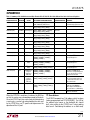
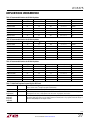
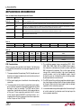
Table 1. Summary of I2C Sub-Addresses and Byte Formats. Bits A7, A6, A5, A4 of Sub-Address Need to be 0 to Access Registers
SUB-ADDRESS
A7A6A5A4A3A2A1A0 OPERATION
ACTION
Global Logic
BYTE FORMAT D7D6D5D4D3D2D1D0
DEFAULT
D7D6D5D4D3D2D1D0 COMMENTS
0000 0000 (00h)
Read/Write
RESET_ALL, DT[1], DT[0], IGNORE_EN, 0000 0000
1KPD, SLOW, RD_TEMP, Unused
0000 0001 (01h)
Read/Write Buck1 Register ENABLE, MODE, PHASE[1], PHASE[0],
DAC[3], DAC[2]. DAC[1], DAC[0]
0000 1100
0000 0010 (02h)
Read/Write Buck2 Register ENABLE, MODE, PHASE[1], PHASE[0],
DAC[3], DAC[2]. DAC[1], DAC[0]
0000 1100
0000 0011 (03h)
Read/Write Buck3 Register ENABLE, MODE, PHASE[1], PHASE[0],
DAC[3], DAC[2]. DAC[1], DAC[0]
0001 1100
0000 0100 (04h)
Read/Write Buck4 Register ENABLE, MODE, PHASE[1], PHASE[0],
DAC[3], DAC[2]. DAC[1], DAC[0]
0001 1100
0000 0101 (05h)
Read/Write Buck5 Register ENABLE, MODE, PHASE[1], PHASE[0],
DAC[3], DAC[2]. DAC[1], DAC[0]
0010 1100
0000 0110 (06h)
Read/Write Buck6 Register ENABLE, MODE, PHASE[1], PHASE[0],
DAC[3], DAC[2]. DAC[1], DAC[0]
0010 1100
0000 0111 (07h)
Read/Write Buck7 Register ENABLE, MODE, PHASE[1], PHASE[0],
DAC[3], DAC[2]. DAC[1], DAC[0]
0011 1100
0000 1000 (08h)
Read/Write Buck8 Register ENABLE, MODE, PHASE[1], PHASE[0],
DAC[3], DAC[2]. DAC[1], DAC[0]
0011 1100
0000 1001 (09h)
Read/Write
RST Mask
PGOOD[8], PGOOD[7], PGOOD[6],
PGOOD[5], PGOOD[4], PGOOD[3],
PGOOD[2], PGOOD[1]
1111 1111
Fault will pull RST low if the
corresponding bit is ‘1’
0000 1010 (0Ah)
Read/Write
IRQ PGOOD
Mask
PGOOD[8], PGOOD[7], PGOOD[6],
PGOOD[5], PGOOD[4], PGOOD[3],
PGOOD[2], PGOOD[1]
0000 0000
Fault will pull IRQ low if the
corresponding bit is ‘1’
0000 1011 (0Bh)
Read/Write
IRQ UVLO
Mask
UVLO[8], UVLO[7], UVLO[6], UVLO[5], 0000 0000
UVLO[4], UVLO[3], UVLO[2], UVLO[1]
Fault will pull IRQ low if the
corresponding bit is ‘1’
0000 1100 (0Ch)
Read
0000 1101 (0Dh)
Read
UVLO Status
Register
(Latched at
IRQ fault)
0000 1110 (0Eh)
Read
Temp Monitor DT_WARN, TEMP[6], TEMP[5],
TEMP[4], TEMP[3], TEMP[2], TEMP[1],
TEMP[0]
0000 1111 (0Fh)
Write
Clear Interrupt
Read back of PGOOD based
faults. If the corresponding mask
bit is ‘0’, then bit can be used to
read back real time data
PGOOD Status PGOOD[8], PGOOD[7], PGOOD[6],
PGOOD[5], PGOOD[4], PGOOD[3],
Register
(Latched at PGOOD[2], PGOOD[1]
IRQ fault)
UVLO[8], UVLO[7], UVLO[6], UVLO[5],
UVLO[4], UVLO[3], UVLO[2], UVLO[1]
Read back of UVLO based faults.
If the corresponding mask bit is
‘0’, then bit can be used to read
back real time data
TEMP bits read back the TEMP
digital code. DT_WARN bit
latches high if an IRQ fault has
been caused due to a DT Warning
NA
When the LTC3375 is read from, it releases the SDA line
so that the master may acknowledge receipt of the data.
Since the LTC3375 only transmits one byte of data during
a read cycle, a master not acknowledging the data sent
by the LTC3375 has no I2C specific consequence on the
operation of the I2C port.
Bits either act at top level or on all
buck switching regulators at once
Clears the Interrupt Bit, Status
Latches are Unlatched
I2C Slave Address
The LTC3375 responds to a 7-bit address which has been
factory programmed to b’0110100[R/WB]’. The LSB of
the address byte, known as the read/write bit, should
be 0 when writing to the LTC3375 and 1 when reading
data from it. Considering the address as an 8-bit word,
3375fc
For more information www.linear.com/3375
21