1
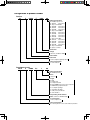
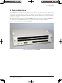
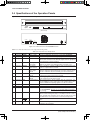
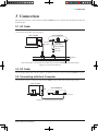
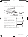
CMOS 4-BIT SINGLE CHIP MICROCOMPUTER
S5U1C63000H6 Manual
(S1C63 Family In-Circuit Emulator)
NOTICE
No part of this material may be reproduced or duplicated in any form or by any means without the written permission
of Seiko Epson. Seiko Epson reserves the right to make changes to this material without notice. Seiko Epson does not
assume any liability of any kind arising out of any inaccuracies contained in this material or due to its application or
use in any product or circuit and, further, there is no representation that this material is applicable to products requiring high level reliability, such as medical products. Moreover, no license to any intellectual property rights is granted by
implication or otherwise, and there is no representation or warranty that anything made in accordance with this material will be free from any patent or copyright infringement of a third party. This material or portions thereof may contain
technology or the subject relating to strategic products under the control of the Foreign Exchange and Foreign Trade
Law of Japan and may require an export license from the Ministry of Economy, Trade and Industry or other approval
from another government agency.
© SEIKO EPSON CORPORATION 2007, All rights reserved.
Configuration of product number
Devices
S1
C
63158
F
0A01
00
Packing specifications
00 : Besides tape & reel
0A : TCP BL
2 directions
0B : Tape & reel BACK
0C : TCP BR
2 directions
0D : TCP BT
2 directions
0E : TCP BD
2 directions
0F : Tape & reel FRONT
0G : TCP BT
4 directions
0H : TCP BD
4 directions
0J : TCP SL
2 directions
0K : TCP SR
2 directions
0L : Tape & reel LEFT
0M : TCP ST
2 directions
0N : TCP SD
2 directions
0P : TCP ST
4 directions
0Q : TCP SD
4 directions
0R : Tape & reel RIGHT
99 : Specs not fixed
Specification
Package
D: die form; F: QFP, B: BGA
Model number
Model name
C: microcomputer, digital products
Product classification
S1: semiconductor
Development tools
S5U1
C
63000
A1
1
00
Packing specifications
00: standard packing
Version
1: Version 1
Tool type
Hx : ICE
Ex : EVA board
Px : Peripheral board
Wx: Flash ROM writer for the microcomputer
Xx : ROM writer peripheral board
Cx : C compiler package
Ax : Assembler package
Dx : Utility tool by the model
Qx : Soft simulator
Corresponding model number
63000: common to S1C63 Family
Tool classification
C: microcomputer use
Product classification
S5U1: development tool for semiconductor products
COnTEnTS
– Contents –
1 Introduction.................................................................................................................... 1
2 S5U1C63000H6 Package ............................................................................................... 2
2.1
2.2
2.3
2.4
Components ...................................................................................................................... 2
Component Specifications ................................................................................................ 3
Environmental Condition for Operation ............................................................................. 3
Specifications of the Operation Panels ............................................................................. 4
3 Connection ..................................................................................................................... 5
3.1
3.2
3.3
3.4
AC Cable ........................................................................................................................... 5
DC Cable ........................................................................................................................... 5
Connection with Host Computer ....................................................................................... 5
Installing Peripheral Circuit Board (S5U1C63xxxP) ......................................................... 6
4 Getting Started .............................................................................................................. 7
5 Operations and Functions of the S5U1C63000H6 ...................................................... 8
5.1 Outline of Operation .......................................................................................................... 8
5.2 Break Function .................................................................................................................. 9
5.3 Monitoring Terminals ......................................................................................................... 9
5.4 Display During Execution and During Break .................................................................... 10
5.5 Break Commands ............................................................................................................ 10
5.6 Target Interrupt and Break................................................................................................ 11
5.7 Trace Function .................................................................................................................. 11
5.8 Trace Mode ....................................................................................................................... 12
5.9 Trace Trigger Point ............................................................................................................ 12
5.10 Coverage Function ......................................................................................................... 12
5.11 Measurement of Execution Time .................................................................................... 12
5.12 Self-Diagnostic Function ................................................................................................ 13
5.13 Restrictions on Emulation .............................................................................................. 13
6 lCD Driver ..................................................................................................................... 16
6.1 Differences from Actual IC ............................................................................................... 16
6.2 Connection with the Target System .................................................................................. 16
7 notes on Use................................................................................................................. 18
7.1 Notes on Operations ........................................................................................................ 18
7.2 Differences from Actual IC ............................................................................................... 18
8 Maintenance and Warranty .......................................................................................... 19
8.1 Self-Diagnostic Test.......................................................................................................... 19
8.2 Warranty ........................................................................................................................... 19
9 Troubleshooting ............................................................................................................ 20
S5U1C63000H6 Manual
(S1C63 Family In-Circuit Emulator)
EPSON
i
1 InTRODUCTIOn
1 Introduction
S5U1C63000H6 (S1C63 Family In-Circuit Emulator) is a hardware tool to effectively develop software for the
S1C63 Family, 4-bit single chip microcomputers. In combination with a peripheral circuit board (S5U1C63xxxP),
it provides the development environment of the software using a personal computer as a host computer, which requires Windows 2000/XP.
This manual describes the operation of the S5U1C63000H6 hardware and connections of the S5U1C63000H6 system. Refer to the “S5U1C63000A Manual” for how to use the control software on the PC (debugger).
Figure 1.1 shows the external view of the S5U1C63000H6.
Figure 1.1 External View of S5U1C63000H6
S5U1C63000H6 Manual
(S1C63 Family In-Circuit Emulator)
EPSON
1
2 S5U1C63000H6 PaCKaGE
2 S5U1C63000H6 Package
2.1 Components
This package is in common with all models of the S1C63 Family. After unpacking the S5U1C63000H6 package,
check to see that all of the following components are included. Figure 2.1.1 shows the package structure.
(1)
(2)
(3)
(4)
(5)
(6)
(7)
(8)
(9)
(10)
(11)
(12)
(13)
S5U1C63000H6 (main unit) ...................................................................... 1 unit
USB cable................................................................................................... 1 cable
AC adapter.................................................................................................. 1 pcs.
AC cable ..................................................................................................... 1 cable
Jig for installing / dismounting board ........................................................ 2 pcs.
S5U1C63000H6 Manual (S1C63 Family In-Circuit Emulator) ................ 1 copy (this manual)
Flat cable with 50-pin × 2 connectors ........................................................ 1 pair
Flat cable with 34-pin × 1 connector.......................................................... 1 pcs.
50-pin connector for target system ............................................................. 2 pcs.
34-pin connector for target system ............................................................. 1 pcs.
User registration card ................................................................................. 1 pcs.
Warranty card ............................................................................................. 1 pcs.
Precautions on using the S5U1C63000H6 ................................................. 1 pcs.
Note that the items listed below are not included in this package. These items need to be provided separately.
(14) S5U1C63xxxP Board (included in the S5U1C63xxxP package)
(15) S5U1C63xxxP Manual (included in the technical manual for each models)
(16) S1C63 Family Debugger (included in the S1C63 Family Assembler package)
(17) S5U1C63000A Manual (included in the S1C63 Family Assembler package)
• S5U1C63000H6
Manual
EPSON
EPSON
S5U1C63000H2 Manual
• User registration card
• Warranty card
• Precautions on using
the S5U1C63000H6
Registration
..............
..........
............
........
S5U1C63000H2 Manual
English
Japanese
Registration
..............
..........
............
........
English
Japanese
OFF
ON
DIAG
LC2
LC1
TR
G
ST OU
OP T
O
TR UT
C
BR IN
K
IN
G
N
D
PO
W
ER
SL EM
P/H U
LT
• S5U1C63000H6 main unit
S5U1C63000H6
• AC adapter
EPSOn
• Connectors
for target system
(50-pin × 2) (34-pin × 1)
• AC cable
• USB cable
• Jigs
• Flat cables
(50-pin × 2)
(× 2)
(34-pin × 1)
Figure 2.1.1 S5U1C63000H6 Package Structure
2
EPSON
S5U1C63000H6 Manual
(S1C63 Family In-Circuit Emulator)
2 S5U1C63000H6 PaCKaGE
2.2 Component Specifications
Table 2.2.1 shows the specifications of the component in the S5U1C63000H6 package.
Table 2.2.1 Specifications of S5U1C63000H6 Components
no.
1
Components
S5U1C63000H6
(main unit)
Items
Dimensions
Weight
External color
Input voltage
Power consumption
Board mounted
2
Interface cable
Length
3
AC adapter
Dimensions
Input voltage
Input frequency
Power consumption
Output voltage,
Current
Length
Plug type
Jig
4
AC cable
5
Accessories
User connector
6
Package
Hardware manual
Warranty card,
User registration card
Dimension
Materials
Specifications
282 mm (W) × 177 mm (D) × 70 mm (H)
Approx. 1.8 kg (main body)
Approx. 3.5 kg (total weight of package)
Cygnus white
DC 12 V
3 A, max.
Main board (included LCD driver) 1 board
USB cable: 1.5 m
LCD cable: 0.4 m
100 mm (W) × 60 mm (D) × 30 mm (H)
AC 90 V to 264 V
50 Hz to 60 Hz ±3 Hz
36 W, max. (in main system load)
DC 12 V,
3 A, with over current protection
1.8 m
2-pin
For installing/dismounting option boards
2 pcs.
3431-6002-LCPL (3M): 1 pcs.
3433-6002-LCPL (3M): 2 pcs.
Remarks
Rubber feet included
Peripheral circuit board
is sold separately.
Outside: 0 V
Inside: 12 V
380 mm (W) × 260 mm (D) × 225 mm (H)
W carton, cardboard
2.3 Environmental Condition for Operation
Table 2.3.1 shows the environmental conditions to operate S5U1C63000H6 that has to be used.
Table 2.3.1 Environmental Conditions
no.
1
2
3
4
5
Items
Operating temperature
Storage temperature
Operation humidity
Storage humidity
Resistance to vibration
S5U1C63000H6 Manual
(S1C63 Family In-Circuit Emulator)
Specifications
5 to 40°C
-10 to 60°C
35 to 80%
20 to 90%
Operating:
Transportation:
EPSON
Remarks
No condensation
0.25 m/s2
1 m/s2
3
2 S5U1C63000H6 PaCKaGE
2.4 Specifications of the Operation Panels
OFF
ON
DIAG
LC2
TR
G
ST OU
OP T
O
TR UT
C
BR IN
K
IN
G
N
D
PO
W
ER
SL EM
P/ U
H
LT
Figure 2.4.1 shows the external view of the panels.
LC1
S5U1C63000H6
EPSOn
(Front view)
POWER
DC 12V
FG
CB
O I
(Rear view)
Figure 2.4.1 External View of S5U1C63000H6 Panels
Table 2.4.1 shows the function of each component on the panels.
Table 2.4.1 Function List of Components
no.
1
2
3
Position
Symbol
name
Function
Front panel POWER
Front panel EMU
Front panel SLP/HLT
Power on LED
This green LED lights upon power-on of the S5U1C63000H6.
Emulation LED
This red LED lights when the target program is in running status.
SLEEP/HALT LED This yellow LED lights when the S1C63000 CPU executes the
HALT or SLP instruction. This LED also lights when the peripheral
circuit board has not been installed.
4 Front panel DIAG
Self-diagnostic
This switch is used to select whether the S5U1C63000H6 selfselect switch
diagnosis at startup of the debugger will be executed or not.
5 Front panel TRGOUT Trace-trigger
Upon coincidence of trigger conditions with a tracing trigger point,
output terminal
a pulse is output from this terminal.
6 Front panel STOPOUT SLEEP/HALT
When the S1C63000 CPU is in HALT or SLEEP status, a low level
status output
signal is output from this terminal. This is used to measure executerminal
tion rate of the CPU. Also this terminal goes low in break status.
7 Front panel TRCIN
Trace input
Trace information will be stored in the trace memory by connecting
terminal
a signal of the target system to this terminal.
8 Front panel BRKIN
Break input
A running program enters break status by input a low level signal
terminal
to this terminal from the target system.
9 Front panel GND
Ground terminal
When monitoring the above terminals with an oscilloscope, connect the GND line of the oscilloscope to this terminal. This is also
used as a GND when inputting signals to the above terminals.
10 Front panel LC1, LC2 LCD connectors
These connectors are used to connect an LCD panel.
11 Rear panel POWER
Power switch
Turns the S5U1C63000H6 power on and off.
12 Rear panel DC12V
DC input connector This connector is used to connect the DC cable of the AC adapter
for S5U1C63000H6. Be sure to use the AC adapter included in
this package.
13 Rear panel CB
Circuit breaker
The breaker cuts off the power of this system (peripheral board,
add-on board and target board) at consumption current of 3 A or
more. A small staff of breaker comes up at the shut-off. The staff
should be at the recessed position for normal operating status.
14 Rear panel
USB connector
This USB cable connector is used to interface with the host computer.
15 Rear panel FG
Frame ground
This is the frame ground terminal. We recommend to connect this
terminal to the ground line.
4
EPSON
S5U1C63000H6 Manual
(S1C63 Family In-Circuit Emulator)
3 COnnECTIOn
3 Connection
This chapter describes the connection between S5U1C63000H6 and a host computer and a Peripheral Circuit Board
(S5U1C63xxxP).
3.1 aC Cable
The S5U1C63000H6 package includes a dedicated AC cable (with 2-pin plug) and AC adapter. The AC cable is
connected into the AC inlet on the AC adapter.
Host computer
S5U1C63000H6
DC 12V
POWER
FG
CB
DC 12V
FG
AC adapter
dedicated for
S5U1C63000H6
DC cable
AC inlet
AC cable
AC line
Frame ground line
* We recommend to connect between the FG terminal of the S5U1C63000H6 and a frame ground.
Figure 3.1.1 Connection of AC Line
3.2 DC Cable
Connect the DC output cable of the AC adapter to the DC12V connector located at the S5U1C63000H6 rear panel.
3.3 Connecting with Host Computer
Connect between the host computer and the S5U1C63000H6 using the USB cable included in this package.
Host computer
S5U1C63000H6
USB
DC 12V
POWER
CB
FG
USB connector
Figure 3.3.1 Connecting with Host Computer
S5U1C63000H6 Manual
(S1C63 Family In-Circuit Emulator)
EPSON
5
3 COnnECTIOn
3.4 Installing Peripheral Circuit Board (S5U1C63xxxP)
By installing the S5U1C63xxxP peripheral circuit board (to be separately sold) into a slot of the S5U1C63000H6, a
debug system can be made corresponding to each device of the S1C63 Family. Figure 3.4.1 shows installing method of the peripheral circuit board. The S5U1C63000H6 is equipped with an LCD driver function, so an LCD board
is not required.
(1), (4)
(2)
LC1
LC2
6
63000H
S5U1C
DIAG
OFF
ON
Peripheral circuit board
(2), (3)
Figure 3.4.1 Installing Peripheral Circuit Board
(1) Unfasten the screws located on the left and right sides of the front panel of the S5U1C63000H6 by turning them
counterclockwise then remove the front panel.
(2) Insert the peripheral circuit board into the slot and push it
using the jig attached with the S5U1C63000H6 as shown
in Figure 3.4.2.
Using this jig as a lever, push it toward the inside of the
board evenly on the left and right sides. After confirming
that the peripheral circuit board has been firmly fitted into
the internal slot of the S5U1C63000H6, remove the jig.
Peripheral circuit board
Figure 3.4.2 Installing Peripheral Circuit Board
(3) When dismounting the peripheral circuit board, set the jig
into position as shown in Figure 3.4.3. Using this jig as a
lever, push it toward the outside of the board evenly on the
left and right sides and pull the peripheral circuit board out
of the S5U1C63000H6.
Peripheral circuit board
(4) Mounting the front panel removed at the step (1) on the
main case by pushing and turning two screws located at
both side.
Figure 3.4.3 Dismounting Peripheral Circuit Board
(5) The jig has a magnet for keeping under the bottom plate of the case while not in use.
6
EPSON
S5U1C63000H6 Manual
(S1C63 Family In-Circuit Emulator)
4 GETTInG STaRTED
4 Getting Started
The S5U1C63000H6 can start using the debugger software after connecting to the host computer.
(1) Setting the DIaG switch
The S5U1C63000H6 has a self-diagnostic function at power-on.
When using this function, set the DIAG switch to ON. To skip the diagnosis, set the switch to OFF.
See Section 5.12, “Self-Diagnostic Function,” for more information on the self-diagnostic function.
(2) Turning the S5U1C63000H6 on
Turn the power switch on. The power LED (green) lights. The SLP/HLT LED (yellow) lights momentarily and
goes out.
(3) Starting the debugger
Launch the debugger on the host computer. The SLP/HLT LED (yellow) lights momentarily and goes out.
(4) Executing the target program
Execute the target program from the debugger. When the target program starts running, the EMU LED (red)
lights to indicate that the S5U1C63000H6 enters emulation mode. When the SLP or HALT instruction is executed, the SLP/HLT LED (yellow) lights.
(5) When a break occurs
When the target program stops at the break point set with the debugger, the EMU LED (red) goes out.
S5U1C63000H6 Manual
(S1C63 Family In-Circuit Emulator)
EPSON
7
5 OPERaTIOnS anD FUnCTIOnS OF THE S5U1C63000H6
5 Operations and Functions of the
S5U1C63000H6
This chapter describes operations, functions in detail and restrictions in the emulation mode of the S5U1C63000H6.
5.1 Outline of Operation
ICE control
processor
ICE firmware
Emulation control portion
Emulation program memory
Emulation data memory
S1C63000
CPU
Trace control unit
Break control unit
Target monitor unit
To peripheral circuit board
Figure 5.1.1 Function Block Diagram of the S5U1C63000H6
The S5U1C63000H6 has a processor to control in-circuit emulation, which processes the commands. The function
to execute or stop target programs by the S1C63000 CPU is called emulation, and it is controlled by the emulation
control unit.
The operating mode while the S1C63000 CPU is running (specified by the G command) or single stepping (specified
by the S or N command) is called emulation mode. The EMU LED lights in this mode. The other status is called
standby mode in which the EMU LED goes out.
The target program to be executed with the S1C63000 CPU is stored in the emulation program memory and
data RAM area of the S1C63000 CPU is assigned to the emulation data memory. In the standby mode, the
S5U1C63000H6 control processor loads the program from the host computer.
The trace control unit consists of a memory of 8,192 words × 120 bits and records execution bus cycles of the
S1C63000 CPU. The memory enables the register value inside the S1C63000 CPU to be real timely recorded. The
program execution is traced in the emulation mode and the traced information is analyzed by the S5U1C63000H6
control processor in the standby mode.
The break control unit compares the bus condition of the S1C63000 CPU with break points and stops the execution
of the target program upon coincident. The break can be also real timely made by register values of the S1C63000
CPU.
While the target program is running, the S5U1C63000H6 control processor monitors the executed program counter
value of the S1C63000 CPU and RAM contents at watching points via the target monitor unit. The monitored results are displayed as on-the-fly information. The S1C63000 CPU can real timely execute the target program while
the information is displayed.
8
EPSON
S5U1C63000H6 Manual
(S1C63 Family In-Circuit Emulator)
5 OPERaTIOnS anD FUnCTIOnS OF THE S5U1C63000H6
5.2 Break Function
(1) Forced break
The debugger on the host computer can forced break the emulation. This function is useful when the program
counter does not proceed by executing the SLP or HALT instruction in a single step process.
(2) Break commands
Some break commands are available to set various breaking condition. A break occurs when the break condition specified by the command and status of the S1C63000 CPU are met.
(3) Break by accessing to undefined area
This break occurs when the target program accesses an address exceeding the ROM capacity of the actual chip.
The break is also occurred when any address other than the RAM area or mapped I/O area of the actual chip is
accessed.
(4) Break by accessing write protect area
This break occurs when the target program writes data to the read only memory such as a character generator
ROM. The memory contents are protected even if this break occurs.
(5) Break by incorrect stack accessing
This break occurs when the target program makes incorrectly stacking operation exceeding the defined stack
area in the S1C63000 CPU.
(6) BRKIn terminal
When a signal is input to the BRKIN terminal, a break occurs at the falling edge of the signal.
5.3 Monitoring Terminals
(1) TRGOUT output terminal
A low level pulse is output at the T3 state of the clock when the trace trigger condition and the bus cycle are
met.
T1
CLK from
peripheral circuit board
T2
T3
T4
PK
PL
Bus cycle
Coincidence with trace trigger
TRGOUT output
Figure 5.3.1 TRGOUT Terminal Output
(2) STOPOUT output terminal
This terminal goes low when the S1C63000 CPU is suspended (by executing of the HALT or SLP instruction).
This terminal also outputs low level during a break.
STOPOUT output
Indicating suspension
of CPU operation
Running
Breaking
Figure 5.3.2 STOPOUT Terminal Output
S5U1C63000H6 Manual
(S1C63 Family In-Circuit Emulator)
EPSON
9
5 OPERaTIOnS anD FUnCTIOnS OF THE S5U1C63000H6
(3) TRnIn input terminal
By connecting a signal line of the target system to this terminal, the signal status is stores in the trace memory
as a trace information. “1” is written to the trace memory when no signal is connected or the signal goes high,
or “0” is written when the signal goes low. The signal level is sampled at the rising edge of T4 state.
(4) BRKIn input terminal
A break occurs when a low level signal is input to this terminal while the target program is running. To use this
terminal for the break function, the low level pulse must be 20 ms or longer. By connecting the TRGOUT output terminal to the BRKIN input terminal, breaks can be occurred according to the trace trigger conditions.
Note: The above output terminals outputs 5.0 V. The input terminals have a pull-up resistor and allow
input of a signal within 3.3 V to 5.0 V.
5.4 Display During Execution and During Break
The S5U1C63000H6 control processor monitors the execution status of the S1C63000 CPU while the target program is running. It displays the S1C63000 CPU’s execution status in every 500 ms when the on-the-fly display
mode is specified. The program counter value that is displayed during break shows the address to be executed in the
next step. The register contents displayed are the values when the previous break occurred.
5.5 Break Commands
The S5U1C63000H6 has abundant break functions.
(1) Program counter break
This break function is specified by the BP command. When the program counter of the S1C63000 CPU coincides with the specified address, a break occurs before executing the instruction. Multiple program counter values (up to maximum size of program memory) can be specified as break points.
(2) Program counter sequential break
This break function is specified by the BS command. A break occurs when the program counter of the
S1C63000 CPU counts three addresses in the specified order. The pass counter can be specified for the last
address. The sequence (address 1 coincidence) → (address 2 coincidence) → (address 3 counted by specified
times) breaks the execution.
(3) Break by data access
This break function is specified by the BD command. A break occurs immediately after the target program accesses the data memory in the specified condition (address, data and read or write operation). It is possible to
specify a range for the address condition, a mask in bit units for the data condition and a mask for the read/
write condition. This specification can set one break point only.
(4) Break by register value
This break function is specified by the BR command. When the register values of the S1C63000 CPU coincide
with the specified values, a break occurs immediately after the instruction is executed. A/B register, E/I/C/Z
flag and X/Y register values can be specified as a break condition. It is also possible to specify masking on each
register. This specification can set one break point only.
The above break functions (1, 2, 3 and 4) can be independently specified. When the target program is executed with
all the BP, BS, BD and BR commands specified, a break occurs by meeting any condition.
10
EPSON
S5U1C63000H6 Manual
(S1C63 Family In-Circuit Emulator)
5 OPERaTIOnS anD FUnCTIOnS OF THE S5U1C63000H6
5.6 Target Interrupt and Break
When an interrupt in the target program and a break are simultaneously occurred, the target interrupt is prioritized.
The break occurs after completing the stack operation of the interrupt. The program counter at the break shows the
top address of the interrupt handler routine. When the target program is restarted, it executes from the top address
of the interrupt handler routine.
If an interrupt and a break are simultaneously occurred when “I” (interrupt flag) = “1” is set as a break condition by
BR command, a break occurs when the “I” flag goes “1.” However, the flags after the break occurred are displayed
as “EICZ: 0000” (the “I” flag is reset) because of the prioritized interrupt process.
5.7 Trace Function
During running in emulation mode, information of the S1C63000 CPU (program counter, instruction code, data
RAM address, data content and CPU register values) is stored into the trace memory at every CPU bus cycle. The
trace memory has a capacity of 8,192 cycles, which can store the latest instructions up to 4,096 in 2 bus-cycle instruction and 2,048 in 4 bus-cycle instruction.
Trace memory
Trace memory
Earliest instruction
(TP = 0)
Effective trace
Effective trace
Execution of
a program
Instruction just before
break (TP = 700)
(TP = 8,191)
Instruction just before break
Earliest instruction
(TP = 0)
Effective trace
Free space
Figure 5.7.1 Trace Function
Figure 5.7.1 shows the trace function. When the trace memory becomes full, old information is erased and new
information is overwritten. TP, which is called trace pointer, shows that the point of 0 means the earliest instruction
and the break point means the latest information. The maximum value of the TP is 8,191.
Trace information
TP = 0
Earliest
instruction
Trace information at any point can be displayed
by the TD command.
TP = 8,191
Latest
instruction
Figure 5.7.2 Trace Pointer
S5U1C63000H6 Manual
(S1C63 Family In-Circuit Emulator)
EPSON
11
5 OPERaTIOnS anD FUnCTIOnS OF THE S5U1C63000H6
5.8 Trace Mode
There are following three trace modes available in the S5U1C63000H6.
(1) all bus cycle trace mode
In this trace mode, all bus cycles are traced during run emulation and step emulation until a break occurs.
(2) Specified program counter range trace mode
In this mode, bus cycles within the specified range (or outside the specified range) are traced during run emulation and step emulation until a break occurs. This function is useful for cases of tracing objective work data
only or removing an WAIT routine from the trace.
(3) Single delay trigger
In this mode, starting a run emulation starts tracing for all bus cycles. When the emulation hit the trace trigger
condition, the trace continues for the specified number of bus cycles, and then it stops. The trace information is
displayed after a break occurs.
In the debugger, one of the above modes can be selected by the TM command.
5.9 Trace Trigger Point
In the S5U1C63000H6, a trace trigger point can be specified independent of break points. The trace trigger point is
specified as the program counter conditions of the S1C63000 CPU. A low level pulse is output from the TRGOUT
terminal with the timing of T3 upon coincidence of the specified value and the program counter. The information of
the trace trigger point is also stored into the trace memory. In the single delay trigger mode, the trace trigger point
becomes a condition for stopping the trace.
5.10 Coverage Function
The S5U1C63000H6 can retrieve and display the address information of the program accessed at the execution.
The confirmation of portions whether failure analysis or debugging is completed or not can be done by checking
the program through reference of the coverage information after running the program for a long time. This function
is specified by the CV or CVC command.
5.11 Measurement of Execution Time
The S5U1C63000H6 has a function to measure the time from start to break of the target program or to count the
number of bus cycles. This function is set by the MD command.
(1) Time measurement mode
• Range of time measurement
1 µs to 1*(231-1) µs (≈ 2,147 seconds ≈ 36 minutes)
• Measurement error
±1 µs
• Units of time display
Micro second (µs) units
(2) Bus cycle count mode
• Range of cycle measurement
1 bus cycle to (231-1) bus cycles (= 2*109 bus cycles)
• Measurement error
0 cycles
12
EPSON
S5U1C63000H6 Manual
(S1C63 Family In-Circuit Emulator)
5 OPERaTIOnS anD FUnCTIOnS OF THE S5U1C63000H6
5.12 Self-Diagnostic Function
The S5U1C6300H6 allows selection whether the self-diagnostic check at power on is performed or not.
(1) Disabling self-diagnostic mode (DIaG switch: OFF)
When the DIAG switch on the S5U1C63000H6 front panel is set to OFF, the S5U1C63000H6 becomes ready
to accept commands without the self-diagnostic check after power on.
(2) Enabling self-diagnostic mode (DIaG switch: On)
When the DIAG switch is set to ON, the S5U1C63000H6 executes the self-diagnostic check shown below after
power on, and then it becomes ready to accept commands.
(a) ROM test
Tests the check-sum of the firmware.
(b) RAM test
Performs the read/write test of the RAM in the S5U1C63000H6.
(c) Emulation test
Tests if a break occurs normally by executing a run emulation for a few steps of instructions on the emulation memory.
When the debugger is started up after the S5U1C63000H6 is turned on with the self-diagnostic mode enabled, the
S5U1C63000H6 performs diagnosis for about one minute. After that, the debugger enters command waiting status.
5.13 Restrictions on Emulation
(1) Timer operation in standby mode
In the emulation with a peripheral circuit board connected to the S5U1C63000H6, the S1C63000 CPU ordinarily idles (standby mode) as shown in Section 5.1. In the standby mode, the S5U1C63000H6 executes the monitor program and the peripheral circuit board is in stop status. The S5U1C63000H6 executes the target program
by the G command and returns to the monitor program after a break occurs.
S1C63000
CPU operation
Monitor program is running
(standby mode)
Target program is running
(emulation mode)
Monitor program is running
(standby mode)
Figure 5.13.1 Operation of S1C63000 CPU
In the models with a built-in timer or watchdog timer, the timer runs only when the target program is executed
if the timer is enabled. Therefore, in the single step operation, the S1C63xxx timer cannot count in real time.
(2) Interrupt in standby mode
In the standby mode, interrupt requests from the target system is reserved. The interrupt while the monitor
program is being executed is accepted at the execution of the target program. For instance, when an interrupt
request from the target system is generated while breaking, the interrupt will be accepted immediately after the
target program restarts if the interrupt is enabled in the S1C63000 CPU.
S5U1C63000H6 Manual
(S1C63 Family In-Circuit Emulator)
EPSON
13
5 OPERaTIOnS anD FUnCTIOnS OF THE S5U1C63000H6
(3) Interrupt at single step operation
Interrupts during single step operation can be enabled or disable using the MD command. Each operation is as
follows.
When interrupt is enabled
If an interrupt request is generated while the target program is single stepping by the S or N command, the
interrupt processing will be started when an instruction is executed, and the execution stops after fetching
the vector address of the interrupt. Therefore, the next single step operation executes the interrupt handler
routine. When the HALT or SLP instruction is executed by the S or N command, the execution is not terminated until an interrupt occurs. In this status, a forced break input from the host computer can suspend the
execution.
When interrupt is disabled
An interrupt processing is not executed by the S command. Therefore, the execution of the HALT or SLP
instruction is immediately suspended, and the program counter indicates the address next to the HALT or
SLP instruction. The N command operates similar to the S command in the execution of the main routine.
However, it enables interrupts while a sub routine is being executed regardless of whether the MD command enables interrupts or not.
(4) Data read from undefined RaM area
When a data RAM (ROM) area or an I/O area that is not available in the actual IC chip is read, the read
data becomes indefinite. Read data from the actual IC is also indefinite, however it is different from the
S5U1C63000H6.
(5) Detection of SP1 incorrect stack access
It is possible to detect any incorrect stack access to out of the SP1 area by specifying the SP1 area with the BSP
command.
The S1C63000 CPU has a queue register and takes stack values in advance in order to make high speed process
of the stacking operation for the CALR instruction and interrupts. Therefore, when restoring a value from the
top address of the stack, the S1C63000 CPU takes a value beyond the top address and writes it into the queue
register. This operation works without any problem. However, the queue register has an indefinite value. In order not to make this process incorrect access, add three to the top address of the SP1 area when specifying.
(6) Data read break
Executing the “INT addr6” instruction issues a dummy read cycle for the memory specified with the addr6 operand. Therefore, a break caused by the dummy read will occur at this instruction when a data read break condition has been specified by the BD command.
14
EPSON
S5U1C63000H6 Manual
(S1C63 Family In-Circuit Emulator)
5 OPERaTIOnS anD FUnCTIOnS OF THE S5U1C63000H6
(7) Register (data) break
The register (data) value after a break occurs may differ from the value set as a register (data) break condition.
The following shows an example if a break condition has been set so that a break will occur when the A register
is set to 5, and when the S1C63000 CPU has executed the sequence in the timing chart shown below to set the A
register to 5 and 6:
CLK
Instruction execution
ld %a, 5
A register
ICE data judgment point
<1>
ld %a, 6
ICE monitor command ICE monitor command
5
6
<2>
<3>
Figure 5.13.2 Example of Register Break
The S5U1C63000H6 judges the register data at the points indicated with a “↑.” It judges that the A register is
“5” at the point of <2>, and the register break condition is met at the same time. However, the S1C63000 CPU
is executing the following “ld %a, 6” instruction at this point and the break occurs after the A register is set to
“6.” Therefore, “6” is read from the A register after the break has occurred. This is also applied to the break by
accessing to undefined area function.
(8) Register (data) break and hardware interrupt
If a hardware interrupt occurs when the register (data) break condition described in Item (7) is met, register (data)
break will occur at the top address of the interrupt handler routine. The following shows an example when a
hardware interrupt factor occurs while the S1C63000 CPU is executing the sequence in the timing chart shown
below to set the A register to 5 and 6, if a break condition has been set so that a register break will occur when
the A register is set to 5:
CLK
Instruction execution
ld %a, 5
A register
ld %a, 6
5
6
<2>
<3>
Interrupt factor
IACK
ICE data judgment point
<1>
Figure 5.13.3 Example When a Register Break and an Interrupt Occur Simultaneously
In the timing chart above, if an interrupt factor occurs (falling edge) at the point of <1>, the S1C63000 CPU
outputs the IACK signal to indicate that an interrupt acknowledgment cycle is executed. The interrupt processing cannot be stopped while IACK is at low level. Therefore, the S5U1C63000H6 cannot disable the interrupt
even if the register break condition (A register = “5”) is met at the point of <2>, as IACK is at low level. The
register break will occur after jumping to the interrupt vector address.
S5U1C63000H6 Manual
(S1C63 Family In-Circuit Emulator)
EPSON
15
6 lCD DRIVER
6 LCD Driver
The S5U1C63000H6 has an LCD driver for emulating built-in LCD driver models.
Note, however, that some functions supported with the S5U1C63000H6 may not be available in the model to be
used. For details of the LCD driver functions, refer to the technical manual for each model.
6.1 Differences from actual IC
Be aware that there are differences on the functions and characteristics from those of the actual IC as shown below.
If they are not taken into consideration, the program may not be operated properly on the actual IC even if there is
no problem on the S5U1C63000H6 with the LCD diver.
(1) Initialization
In the actual IC, contents of the LCD segment memory are indefinite at system reset and the output LCD drive
waveform is also indefinite according to the memory contents. It means that the segment memory and the LCD
drive waveforms are coincident even though both are indefinite. However, in the S5U1C63000H6, the segment
memory and the output LCD drive waveform are not coincident. Therefore, be sure to create the initial routine
so that the LCD segment memory will be cleared (or set) after a system reset.
(2) lCD segment RaM (for models in which the memory-bit assignment for the LCD segments is fixed)
In the actual IC, when reading a segment memory address that contains both the bits assigned for the LCD segments and the bits not assigned, the unassigned bits are always read as “0.” However, in the S5U1C63000H6,
the unassigned bits in the segment memory can be read and written as memory bits. Therefore, the program
must ignore these unassigned bit values when a segment memory word is read out.
(3) Drive capability of SEG and COM terminals
The output drive capability of the SEG and COM terminals in the S5U1C63000H6 is different from that of the
actual IC. The S5U1C6300H6 cannot be used for evaluating electrical characteristics. The system should be designed in consideration of the electrical characteristics described in the technical manual of each model.
(4) lCD dive voltage
The LCD drive voltage in the S5U1C63000H6 may differ from that of the actual IC.
6.2 Connection with the Target System
Use the supplied connection cables (100-pin/50-pin × 2 flat type, 34-pin flat type) to connect between the
S5U1C63000H6 and the LCD connectors on the target board.
mark
Connection cable
mark
CN4-1
(50-pin)
CN4-2
(50-pin)
CN5
(34-pin)
To target board
Figure 6.2.1 Connecting with the Target System
16
EPSON
S5U1C63000H6 Manual
(S1C63 Family In-Circuit Emulator)
6 lCD DRIVER
Connector pin assignments
Table 6.2.1 LC1 Connector (100-pin/50-pin × 2 flat type)
lC1 connector (Cn4-1)
no.
Signal name
lC1 connector (Cn4-2)
no.
Signal name
1
2
3
4
5
6
7
8
9
10
11
12
13
14
15
16
17
18
19
20
21
22
23
24
25
26
27
28
29
30
31
32
33
34
35
36
37
38
39
40
41
42
43
44
45
46
47
48
49
50
1
2
3
4
5
6
7
8
9
10
11
12
13
14
15
16
17
18
19
20
21
22
23
24
25
26
27
28
29
30
31
32
33
34
35
36
37
38
39
40
41
42
43
44
45
46
47
48
49
50
COM0
COM1
COM2
COM3
COM4
COM5
COM6
COM7
SEG0
SEG1
SEG2
SEG3
SEG4
SEG5
SEG6
SEG7
SEG8
SEG9
SEG10
SEG11
SEG12
SEG13
SEG14
SEG15
SEG16
SEG17
SEG18
SEG19
SEG20
SEG21
SEG22
SEG23
SEG24
SEG25
SEG26
SEG27
SEG28
SEG29
SEG30
SEG31
SEG32
SEG33
SEG34
SEG35
SEG36
SEG37
SEG38
SEG39
SEG40
SEG41
S5U1C63000H6 Manual
(S1C63 Family In-Circuit Emulator)
SEG42
SEG43
SEG44
SEG45
SEG46
SEG47
SEG48
SEG49
SEG50
SEG51
SEG52
SEG53
SEG54
SEG55
SEG56
SEG57
SEG58
SEG59
SEG60
SEG61
SEG62
SEG63
SEG64
SEG65
SEG66
SEG67
SEG68
SEG69
SEG70
SEG71
SEG72
SEG73
SEG74
SEG75
SEG76
SEG77
SEG78
SEG79
Cannot be connected
Cannot be connected
Cannot be connected
Cannot be connected
Cannot be connected
Cannot be connected
Cannot be connected
Cannot be connected
Cannot be connected
Cannot be connected
Cannot be connected
Cannot be connected
EPSON
Table 6.2.2 LC2 Connector (34-pin flat type)
no.
1
2
3
4
5
6
7
8
9
10
11
12
13
14
15
16
17
18
19
20
21
22
23
24
25
26
27
28
29
30
31
32
33
34
lC2 connector (Cn5)
Signal name
COM0
COM1
COM2
COM3
COM4
COM5
COM6
COM7
COM8
COM9
COM10
COM11
COM12
COM13
COM14
COM15
COM16
COM17
COM18
COM19
COM20
COM21
COM22
COM23
COM24
COM25
COM26
COM27
COM28
COM29
COM30
COM31
Cannot be connected
Cannot be connected
Note that some signals do not exist
in the actual IC depending on the
model.
The COM0–COM7 pins are available in the both connectors CN4-1
and CN5, and either one can be
used.
17
7 nOTES On USE
7 Notes on Use
Pay attention to the following matters for proper use of the S5U1C63000H6.
7.1 notes on Operations
(1) Connecting and disconnecting the units
Make sure that the S5U1C63000H6 is turned off when installing the peripheral circuit board (S5U1C63xxxP)
and connecting/disconnecting the cables, as hot insertion/removal may damage the IC.
(2) Turning power on and off
When turning the S5U1C63000H6 off and on again, wait at least 10 seconds before turning on. If power is
turned on without an interval, the power-on-reset sequence may not be executed normally and the result is that
the S5U1C63000H6 fails to function normally, or the circuit breaker on the S5U1C63000H6 may trip.
(3) Peripheral circuit board (S5U1C63xxxP)
A peripheral circuit board is required to operate the S5U1C63000H6. The S5U1C63000H6 package does not
include a peripheral circuit board, so it must be prepared separately. If the S5U1C63000H6 is turned on without
a peripheral circuit board installed, the “SLP/HLT” LED on the S5U1C63000H6 front panel lights.
(4) Over current protection
If the S5U1C63000H6 is turned on when VDD and VSS are short-circuited on the target system, the over current
protection function of the dedicated AC adapter works to cut off its output current and the power LED does not
light. The circuit breaker cuts the power at the load current of 3 A or more on the target system.
7.2 Differences from actual IC
(1) Initialization of RaM
The data RAM of the actual IC is not initialized at system reset, however, the S5U1C63000H6 initializes the
RAM with “0A.” Therefore, be sure to initialize the RAM in the target program, and do not create a program
depending on the initial value.
(2) Initialization of registers
In the actual IC, the CPU registers are not initialized at power on. At initial reset, they keep values prior to the
reset expect the program counter (PC), the interrupt flag (I) and the extension flag (E). However, the CPU registers in the S5U1C63000H6 are initialized to “0A” (4-bit), “0AA” (8-bit) and “0AAAA” (16-bit) at the power
on and at a software reset by the debugger command. Therefore, be sure to initialize the registers, and do not
create a program depending on the initial value. The reset switch on the peripheral circuit board and the hardware reset input from the I/O connector keep values prior to the reset the same as the actual IC.
(3) access to undefined area
In the S5U1C63000H6, a break occurs if an undefined area is accessed. However, a RAM is included in the
undefined area and an undefined area break occurs after the area has been accessed, so any data can be written
to the undefined area. When the target program is restarted after an undefined area break has occurred, it works
using a memory area that does not exists in the actual IC. Therefore, be sure to avoid reading/writing from/to
undefined area by the target program.
(4) Data dump
The S5U1C63000H6 uses a peripheral circuit board clock for accessing a RAM, ROM, LCD or I/O area with a
data dump command. Therefore, the value of the I/O area read in the target program may differ from the value
read by a dump command, when an I/O area that develops a delay until the correct value is obtained due to the
parasitic capacitance and the pull-up/down resistor of the I/O terminal.
18
EPSON
S5U1C63000H6 Manual
(S1C63 Family In-Circuit Emulator)
8 MaInTEnanCE anD WaRRanTY
8 Maintenance and Warranty
8.1 Self-Diagnostic Test
The self-diagnostic test is executed by starting the debugger after setting the DIAG switch on the front panel to “ON”
position and then turning the S5U1C63000H6 on.
The debugger displays the messages shown below during the start-up sequence.
Debugger for S1C63 Ver. x.xx
Copyright (C) SEIKO EPSON CORP. 1998-xxxx
Connecting USB ... done
DIAG test, please wait 1 min ... done
← <1>
Parameter file name
: Par63xxx.par
Version
: xx
Chip name : xxxxx
CPU version
: x.x
PRC board version
: x.x
LCD board version
: x.x
EXT board version
: x.x
ICE hardware version
: x.x
ICE software version
: x.x
DIAG test
: OK.
Map ............................. done
Initialize ...................... done
>
When an error is detected in the diagnosis, the error message is displayed at the point <1> instead of “done.”
If an error message is displayed, stop using the S5U1C63000H6, as it may have a hardware failure.
This self-diagnostic test takes about one minute for its precise inspection until it is completed and the
S5U1C63000H6 is ready to accept commands.
8.2 Warranty
Please refer to the warranty card included in the package for the warranty details.
S5U1C63000H6 Manual
(S1C63 Family In-Circuit Emulator)
EPSON
19
9 TROUBlESHOOTInG
9 Troubleshooting
Following shows some hardware errors and their possible causes.
(1) a message of “connecting USB ... failure” is displayed at start-up of the debugger.
• Is power of the S5U1C63000H6 on?
• Is the circuit breaker (CB) off?
• Is the host cable connected correctly?
• Is the target cable connected correctly?
• Is the peripheral circuit board insert firmly?
(2) The circuit breaker (CB) trips and the POWER lED goes out when the S5U1C63000H6 is
turned on.
• Is the target cable connected correctly?
• Is VDD and VSS short-circuited on the target board?
Refer to the “S5U1C63000A Manual” for operations of the debugger.
20
EPSON
S5U1C63000H6 Manual
(S1C63 Family In-Circuit Emulator)
International Sales Operations
AMERICA
ASIA
EPSON ELECTRONICS AMERICA, INC.
EPSON (CHINA) CO., LTD.
23F, Beijing Silver Tower 2# North RD DongSanHuan
ChaoYang District, Beijing, CHINA
Phone: +86-10-6410-6655
Fax: +86-10-6410-7320
HEADQUARTERS
2580 Orchard Parkway
San Jose, CA 95131, U.S.A.
Phone: +1-800-228-3964
Fax: +1-408-922-0238
SALES OFFICE
Northeast
301 Edgewater Place, Suite 210
Wakefield, MA 01880, U.S.A.
Phone: +1-800-922-7667
Fax: +1-781-246-5443
EUROPE
EPSON EUROPE ELECTRONICS GmbH
HEADQUARTERS
Riesstrasse 15
80992 Munich, GERMANY
Phone: +49-89-14005-0
Fax: +49-89-14005-110
SHANGHAI BRANCH
7F, High-Tech Bldg., 900, Yishan Road
Shanghai 200233, CHINA
Phone: +86-21-5423-5522
Fax: +86-21-5423-5512
EPSON HONG KONG LTD.
20/F, Harbour Centre, 25 Harbour Road
Wanchai, Hong Kong
Phone: +852-2585-4600
Fax: +852-2827-4346
Telex: 65542 EPSCO HX
EPSON Electronic Technology Development
(Shenzhen) LTD.
12/F, Dawning Mansion, Keji South 12th Road
Hi- Tech Park, Shenzhen
Phone: +86-755-2699-3828
Fax: +86-755-2699-3838
EPSON TAIWAN TECHNOLOGY & TRADING LTD.
14F, No. 7, Song Ren Road
Taipei 110
Phone: +886-2-8786-6688
Fax: +886-2-8786-6660
EPSON SINGAPORE PTE., LTD.
1 HarbourFront Place
#03-02 HarbourFront Tower One, Singapore 098633
Phone: +65-6586-5500
Fax: +65-6271-3182
SEIKO EPSON CORPORATION
KOREA OFFICE
50F, KLI 63 Bldg., 60 Yoido-dong
Youngdeungpo-Ku, Seoul, 150-763, KOREA
Phone: +82-2-784-6027
Fax: +82-2-767-3677
GUMI OFFICE
2F, Grand B/D, 457-4 Songjeong-dong
Gumi-City, KOREA
Phone: +82-54-454-6027
Fax: +82-54-454-6093
SEIKO EPSON CORPORATION
SEMICONDUCTOR OPERATIONS DIVISION
IC Sales Dept.
IC International Sales Group
421-8, Hino, Hino-shi, Tokyo 191-8501, JAPAN
Phone: +81-42-587-5814
Fax: +81-42-587-5117
S5U1C63000H6 Manual
(S1C63 Family In-Circuit Emulator)
SEMICONDUCTOR OPERATIONS DIVISION
EPSON Electronic Devices Website
http://www.epson.jp/device/semicon_e
Document code: 411189600
Issue September, 2007
Printed in Japan
L
A