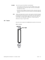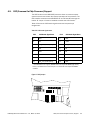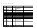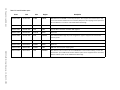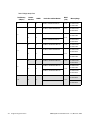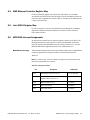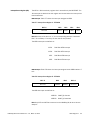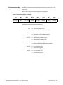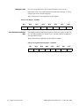
1
HW400p/M
A High-Performance PCI Communications Controller
Technical Reference, Rev. 1.0, March 6, 2002
Primary Text Number M8239
SBE, Inc.
2305 Camino Ramon #200, San Ramon, California 94583
(925) 355-2000
Technical Support (800) 444-0990
Fax: (925) 355-2020
FaxBack Service: (800) 214-4723
Website: http://www.sbei.com
Copyright ©2002 by SBE, Inc. All rights reserved.
No part of this manual may be reproduced by any means without written
permission from SBE, Inc., except that the purchaser may copy necessary
portions for internal use only.
While every effort has been made to ensure the accuracy of this manual, SBE
cannot be held responsible for damage resulting from information herein. All
specifications are subject to change without notice.
SBE, Inc. and the SBE logo are trademarks of SBE, Inc.
All other trademarks and copyrights are owned by their respective companies.
About SBE, Inc. SBE, Inc., provides a broad range of intelligent communications
controllers used primarily in networking systems applications. These products
are sold worldwide through direct sales and distribution channels.
SBE is based in San Ramon, California, and can be reached at 925-355-2000
or online at http://www.sbei.com
2
HW400p/M Technical Reference - 1.0, March 6, 2002
Contents
1. About This Manual ..................................................................................................................................... 7
1-1. Related Documents ..............................................................................................................................7
1-2. Documentation Conventions ................................................................................................................8
2. HW400p/M Introduction ........................................................................................................................... 9
2-1. Functional Components ........................................................................................................................9
3. Specifications ...........................................................................................................................................11
3-1. Processor ............................................................................................................................................ 11
Motorola MPC8245 ........................................................................................................................ 11
3-2. Memory ............................................................................................................................................... 12
Synchronous DRAM ........................................................................................................................ 12
Boot PROM ...................................................................................................................................... 12
EEPROM ........................................................................................................................................... 12
High-density Flash ........................................................................................................................... 12
3-3. I/O ....................................................................................................................................................... 13
DUART .............................................................................................................................................. 13
10/100 Mbps Ethernet/Am79C973 ............................................................................................. 13
Intel 21554 PCI-to-PCI Bridge ........................................................................................................ 13
3-4. Operating Requirements ................................................................................................................... 14
3-5. Power Requirements .......................................................................................................................... 14
3-6. Physical Characteristics ..................................................................................................................... 15
3-7. Mean Time Between Failures ............................................................................................................ 16
3-8. Compliance ......................................................................................................................................... 16
Industry standards compliance ..................................................................................................... 16
3-9. Certifications ...................................................................................................................................... 16
Safety ............................................................................................................................................... 16
Emissions ........................................................................................................................................ 16
Telecom ........................................................................................................................................... 17
Industry Canada CS03 .................................................................................................................... 18
Agency compliance ......................................................................................................................... 18
3-10. Software Support ............................................................................................................................. 19
3-11. Returns/Service ............................................................................................................................... 19
4. Functional Information ............................................................................................................................21
4-1. MPC8245 ........................................................................................................................................... 21
Development/debug support ......................................................................................................... 21
Reset ................................................................................................................................................ 21
Download and console ports ......................................................................................................... 21
4-2. PMC Site ............................................................................................................................................. 21
Compatible PMC modules .............................................................................................................. 21
Voltage keying ................................................................................................................................. 21
EMI requirements ........................................................................................................................... 22
4-3. PCI–to-PCI Bridge ............................................................................................................................... 23
HW400p/M Technical Reference - 1.0, March 6, 2002
Contents
3
PCI interface .................................................................................................................................... 23
Local PCI bus ................................................................................................................................... 23
21554 initialization without serial preload ................................................................................... 23
4-4. LEDs .................................................................................................................................................... 24
4-5. I/O Bus ................................................................................................................................................ 26
DUART .............................................................................................................................................. 26
EEPROM ........................................................................................................................................... 26
Flash ROM ....................................................................................................................................... 27
CPLD ................................................................................................................................................ 27
4-6. Panels ................................................................................................................................................. 27
4-7. I/O Bus Control and Miscellaneous Logic ........................................................................................ 28
I/O registers .................................................................................................................................... 28
Power up and reset ......................................................................................................................... 29
4-8. Connectors ......................................................................................................................................... 29
Ethernet connector ......................................................................................................................... 29
PCI connectors ................................................................................................................................ 29
4-9. COP (Common On-Chip Processor) Support ..................................................................................... 33
5. Programming Information .......................................................................................................................34
5-1. MPC8245 Memory Map .................................................................................................................... 34
Master window ................................................................................................................................ 34
8-bit peripheral devices .................................................................................................................. 34
16-bit peripheral devices ............................................................................................................... 34
Master PCI memory (MPCIM) ......................................................................................................... 34
5-2. Local PCI Address Space Map ........................................................................................................... 36
Firmware .......................................................................................................................................... 36
Masters ............................................................................................................................................ 36
Master windows .............................................................................................................................. 36
5-3. High-Density Flash ............................................................................................................................. 39
5-4. AMD Ethernet Controller Register Map ............................................................................................ 41
5-5. Intel 21554 Register Map ................................................................................................................. 41
5-6. MPC8245 Interrupt Assignments ..................................................................................................... 41
MPC8245 interrupt routing ............................................................................................................ 41
5-7. CPLD Registers ................................................................................................................................... 42
Interrupt Source Register (ISR) ...................................................................................................... 43
Interrupt Enable Register A (IERA) ................................................................................................. 44
Interrupt Enable Register B (IERB) ................................................................................................ 44
Board Status Register (BSR) .......................................................................................................... 45
LED Registers (LED) ........................................................................................................................ 46
Geographic Addressing Register (GAR) ......................................................................................... 46
Port Option Register (POR) ............................................................................................................. 47
Board Option Register (BOR) .......................................................................................................... 48
General Purpose Register (GPR) .................................................................................................... 49
4
Contents
HW400p/M Technical Reference - 1.0, March 6, 2002
Figures
Figure 2-1
Figure 3-1
Figure 3-2
Figure 4-1
Figure 4-2
Figure 4-3
Figure 4-4
Figure 4-5
HW400p/M functional block diagram.................................................................................................... 10
HW400p/M board layout......................................................................................................................... 11
HW400p/M dimensions .......................................................................................................................... 15
Voltage keying .......................................................................................................................................... 22
Voltage key post screw ............................................................................................................................ 22
Board LEDs ............................................................................................................................................... 25
I/O panel................................................................................................................................................... 27
COP jumpers............................................................................................................................................. 33
HW400p/M Technical Reference - 1.0, March 6, 2002
Contents
5
Tables
Table 3-1
Table 3-2
Table 3-3
Table 4-1
Table 4-2
Table 4-3
Table 4-4
Table 4-5
Table 4-6
Table 4-7
Table 4-8
Table 5-1
Table 5-2
Table 5-3
Table 5-4
Table 5-5
Table 5-6
Table 5-7
Table 5-8
Table 5-9
Table 5-10
Table 5-11
Table 5-12
Table 5-13
Table 5-14
Table 5-15
Table 5-16
Operating requirements........................................................................................................................... 14
Power requirements................................................................................................................................. 14
HW400p/M physical characteristics ...................................................................................................... 15
PCI configuration access bit definitions ................................................................................................. 23
LEDs .......................................................................................................................................................... 24
EEPROM address ranges......................................................................................................................... 26
I/O registers.............................................................................................................................................. 28
Devices affected by power up and reset types ...................................................................................... 29
PCI connector P1 pin assignments ......................................................................................................... 30
MPC8245 debug connector pin assignments ....................................................................................... 32
COP header signal names ....................................................................................................................... 33
MPC8245 local address space memory map........................................................................................ 35
Masters and window access regions...................................................................................................... 36
Local PCI address space.......................................................................................................................... 38
High-density Flash.................................................................................................................................... 40
Interrupt pin functions ............................................................................................................................. 41
I/O registers.............................................................................................................................................. 42
Interrupt Source Register A – FFE20000............................................................................................... 43
Interrupt Source Register B – FFE20001............................................................................................... 43
Interrupt Enable Register A – FFE20003 ............................................................................................... 44
Interrupt Enable Register B – FFE20004............................................................................................... 44
Board Status Register – FFE20005 ....................................................................................................... 45
LED Register – FFE20006....................................................................................................................... 46
Geographic Addressing Register – FFE20008....................................................................................... 46
Port Option Register – FFE2000C .......................................................................................................... 47
Board Option Register – FFE2000D ....................................................................................................... 48
General Purpose Register—FFE2000E ................................................................................................... 49
Contents
HW400p/M Technical Reference - 1.0, March 6, 2002
-
6
1. About This Manual
This manual is the technical reference for the HW400p/M communications
controller for the PCI bus. This manual is intended for hardware engineers
who are incorporating the HW400p/M into a system.
The HW400p/M Technical Reference includes:
• Introduction and background on the HW400p/M communications
controller and SBE, Inc.
• Specifications and physical characteristics of the controller
• Support information
• Installation instructions
• Programming information
1-1. Related Documents
• PCI Local Bus Specification Rev. 2.1, June 1, 1995.
• IEEE 1386-2001, Standard for a Common Mezzanine Card (CMC),
Aug. 21, 2001, IEEE.
• IEEE 1386.1-2001, Standard Physical and Environmental Layers for PCI
Mezzanine Cards (PMC), Aug. 16, 2001, IEEE.
• MPC8245 Integrated Processor User’s Manual, October 2001, Rev. 1.0.
• Intel 21554 PCI-PCI Bridge Hardware Reference Manual, Sept. 1998.
• AMD Am79C973/Am79C975 Single-Chip 10/100 Mbps PCI Ethernet
Controller with Integrated PHY.
• 3 Volt Advanced+ Boot Block Flash Memory Data Sheet, October 2001,
Intel.
HW400p/M Technical Reference - 1.0, March 6, 2002
Related Documents
7
1-2. Documentation Conventions
Registers
Register bits are numbered starting with 0. Bit 0 is the
least significant and bit 7 is the most significant bit of a
byte. Unless otherwise noted, register bits that are
identified as “unused” do not affect the function of the
register, and, if read, yield no information.
Signals
When referring to a signal function in text, signal names do
not indicate polarity, and the / is not used. Occasionally a
signal name may be followed by an asterisk (*), a pound
sign (#), a # after the name, or with a / in front of the signal
name. These are valid ways of indicating active low signals.
Code
Code is represented in Courier
typeface.
Placeholders
Placeholders are represented in italic typeface.
Throughout this manual you may find notes, cautions, and warnings that
emphasize certain portions of the material presented in the text.
Note: Provides information that is important to the surrounding text.
Caution!
8
About This Manual
Points out possible ways the product can be damaged if proper precautions
are not followed.
HW400p/M Technical Reference - 1.0, March 6, 2002
2. HW400p/M Introduction
The HW400p/M is a member of SBE’s HighWire™ product line, a family of
high-performance communications products.
The HW400p/M is a network interface and protocol processing product with
these characteristics:
• PCI variable length form factor
• A single PMC site
• PCI 2.1 host interface
• Architecture and software similarity with HW400
2-1. Functional Components
The HW400p/M includes these functional components:
• Motorola MPC8245 on-board processor
• Intel 21554 PCI-PCI bridge module
• 10/100base-Tx Ethernet port
• PCI 2.1 host interface
Figure 2-1 shows the functional block diagram for the HW400p/M.
HW400p/M Technical Reference - 1.0, March 6, 2002
Functional Components
9
Figure 2-1 HW400p/M functional block diagram
Development/Debug
LEDs
Ports
Optional
DUART
CPLD
EEPROM
Flash/OTP
Flash
ROM
NVRAM
SDRAM
I/O Bus and Ctrls
For Development Only
LEDs
10BaseT/
Am79C973
PMC Connectors
100BaseTx
Ethernet
Jn1 and Jn2
MPC8245
Processor
Controller
RJ-45
Xfrmr
Local/Secondary PCI Bus
21554
PCI-to-PCI Bridge
Host/Primary PCI Bus
Connector
10
HW400p/M Introduction
HW400p/M Technical Reference - 1.0, March 6, 2002
3. Specifications
This chapter details the physical characteristics and specifications for the
HW400p/M communications controller.
Figure 3-1 shows the HW400p/M board layout. See Figure 2-1 for a
HW400p/M functional block diagram.
Figure 3-1 HW400p/M board layout
RJ45 connector
Debug connector
Ethernet LEDS (4x)
U65
J9
Dual-color
U66
J8
Altera
status LED
CPLD
EPM3256
MPC8245
AM79C973
JN2
JN1
21554
Intel
PCI Bridge
M2
M4
(3.3V)
(5V)
3-1. Processor
Motorola MPC8245
The main controller is the Motorola MPC8245, which consists of:
• PowerPC 603e core operating at 333MHz
• 32-bit PCI interface operating at 33MHz
• SDRAM memory controller supporting SDRAMs and operating at 133MHz
• General purpose I/O and ROM interface
• Two-channel DMA controller
• Programmable interrupt controller with multiple timers and counters
HW400p/M Technical Reference - 1.0, March 6, 2002
Processor
11
3-2. Memory
The HW400p/M contains a variety of memory devices for use by the
MPC8245. Their characteristics are described in the following sections.
Synchronous DRAM
The synchronous DRAM provides the following features:
• 133MHz operation
• 64MB organized as a single bank of four 8M x 16 devices
• No parity
Boot PROM
The boot PROM provides the following features:
• The Flash implementation uses two byte-wide devices
• PLCC devices (29LV010 or 29LV040) socketed
• 3.3V LVTTL-compatible
• Attached to the local I/O bus of the MPC8245
• U65 and U66 PCB reference designators (U66 is accessed by processor
at power up)
EEPROM
The EEPROM provides the following features:
• A 2k x 8 parallel device, used for the retention of manufacturing
identification information
• 250nsec
• Attached to the local I/O bus of the MPC8245
High-density Flash
Two Intel 3V Advance+ Boot Block Flash devices are used, the
TE28F320C3B100A.
The optional high-density Flash provides the following features:
• 48-pin TSOP with an access time of 100nsec or better
• 0/2/4/8 Mbytes organized as 0/512KB/1MB/2MB x 16 bits
12
Specifications
HW400p/M Technical Reference - 1.0, March 6, 2002
3-3. I/O
DUART
10/100 Mbps Ethernet/Am79C973
The Exar ST16C2550 Dual Universal Asynchronous Receiver/Transmitter
(DUART) provides connectivity to the two serial ports via a console accessory
kit.
The Am79C973 controller is a single-chip 32-bit full-duplex, 10/100-Mbps
fully integrated PCI-to-Wire Fast Ethernet controller.
The Am79C973 controller provides the following features:
• An Ethernet circuit that supports either 10BaseT or 100BaseTx
• Integrates the complete 10/100 PHY interface
• The internal 10/100 PHY implements Auto-Negotiation for twisted-pair
(10T/100X) operating as defined in the IEEE 802.3u specification
• 12k buffers
• 32-bit 33MHz PCI bus interface
• Four LEDS indicating the Ethernet status are surface-mounted on the
board along the top edge of the PCB near RJ-45 (see Section 4-4, LEDs)
• Accessible through RJ-45 (not front panel accessible)
Intel 21554 PCI-to-PCI Bridge
The PCI bus interface is implemented using the Intel 21554 PCI/PCI
Translation Bridge chip operating at 33MHz on both the host PCI and local
PCI.
The PCI bus interface provides the following features:
• The 21554 is a PCI master or slave for memory and I/O accesses on a
33MHz/32- or 64-bit PCI bus
• 32-bit local bus
• A universal signaling device that operates at 3.3V but is also 5.0-V I/Otolerant
• A nontransparent PCI-to-PCI bridge that allows a local processor to
independently configure and control a local subsystem
HW400p/M Technical Reference - 1.0, March 6, 2002
I/O
13
3-4. Operating Requirements
Table 3-1 Operating requirements
Operating Requirement
Caution!
Acceptable Range or Value
Storage temperature
−40 to +85° C (−40 to 185° F)
Cold start temperature
0 to 55° C (32 to 131° F)
Operating temperature
−5 to 55° C (23 to 131° F)
(at board surface with power applied)
Relative humidity
20% to 80% noncondensing
Storage humidity
10% to 95% noncondensing
Power requirements
13 watts maximum, without a PMC module
Bring the HW400p/M communications controller to operating temperature in
a noncondensing environment. The rate of change in board temperature
should not exceed 2° C (35.6 °F) per minute.
3-5. Power Requirements
The power requirements of the HW400p/M are 13 watts maximum, without a
PMC module.
Table 3-2 Power requirements
14
Specifications
Voltage
5.0V
Tolerance
±5%
4.75V to 5.25V
Max Current
2.75A at 4.75V
HW400p/M Technical Reference - 1.0, March 6, 2002
3-6. Physical Characteristics
Table 3-3 provides the HW400p/M board’s parameters and dimensions.
Table 3-3 HW400p/M physical characteristics
Parameter
Dimension
Length
8.661 inches (22 cm)
Height
4.25 inches (10.8 cm)
Maximum component height
(front)
0.570 inches (1.448 cm)
Maximum component height
(back)
0.105 inches (0.267 cm)
Board thickness
0.062 inches ± 0.005 inches
(0.157 cm ± 0.0127 cm)
Figure 3-2 HW400p/M dimensions
8.661″ (22 cm)
4.25″ (10.8 cm)
HW400p/M Technical Reference - 1.0, March 6, 2002
Physical Characteristics
15
3-7. Mean Time Between Failures
The part failure source rate was calculated in accordance with the TELCORDIA
TECHNOLOGIES Specification TR-332, version 6. This is based on an ambient
temperature of 40 °C in a benign controlled environment, using Quality Level
II parts.
The mean time between failures for the HW400p/M is greater than or equal
to 275,000 hours.
3-8. Compliance
Industry standards compliance
HW400p/M complies with the following industry standard specifications:
• PCI Special Interest Group, “PCI Local Bus Specification,” Rev. 2.1,
June 1995.
• IEEE P1386 Common Mezzanine Card Standard.
• IEEE P1386.1 Physical and Environmental Layers for PCI Mezzanine
Cards.
• GR-63-CORE, “Network Equipment-Building Systems (NEBS)
Requirements: Physical Protection,” Issue 1, October 1995.
3-9. Certifications
All certifications described in the following sections are pending.
Safety
Tested to Comply with
IEC 60950:1991+A1:1992+A2:1993+A3:1995+A4:1996
(CB Report Reference No. XXXXXX - PENDING)
UL 1950 Edition 3 and cUL. This adapter is a UL-listed accessory (UL File No.
PENDING) and is for use only with UL-listed computers, workstations, network
servers, etc. that have installation instructions that detail how to install
adapter cards.
Emissions
EN 50082-1 and EN55022 (Report JTN PENDING).
CC Part 15, Subpart B. This equipment generates, uses and can radiate radio
frequency energy, and, if not installed properly and used in accordance with
instructions contained in this manual, may cause harmful interference to
radio communications. This device was tested and found to comply with the
limits for a Class A Computing Device, in accordance with the specification in
Part 15 of FCC Rules.
Operation of this equipment in a residential area is likely to cause harmful
interference. The user will be required to correct the interference at his or her
own expense.
16
Specifications
HW400p/M Technical Reference - 1.0, March 6, 2002
Telecom
CTR13 (includes CTR12 and ETS 300046; −2.048 Mbit/s structured 120 ohm)
(Registration No. PENDING).
FCC Part 68. This device was tested and found to comply with Part 68 of FCC
Rules. A label can be found on the back of the board near the RJ45 connector.
This label contains the FCC Registration Number for this unit. You must, upon
request, provide this information to your telephone company.
FCC Registration Number PENDING
USOC Jack RJ48C
Note: An FCC Modular Jack is provided with this equipment. This equipment is
designed to be connected to the telephone network or premises wiring using
a compatible modular plug. See installation instructions, under separate
cover, for details.
If this equipment causes harm to the telephone network, the telephone
company will notify you in advance that temporary discontinuance of service
may be required. But if advance notice is not practical, the telephone
company will notify the customer as soon as possible. Also, you will be
advised of your right to file a complaint with the FCC if you believe it is
necessary.
The telephone company may make changes in its facilities, equipment,
operations, or procedures that could affect the operation of the equipment. If
this happens, the telephone company will provide advance notice in order for
you to make the necessary modifications so as to maintain uninterrupted
service.
If trouble is experienced with the HW400, contact SBE, Inc., at 1-800-9252666. If the equipment is causing harm to the network, the telephone
company may request you to remove the equipment from the network until
the problem is resolved.
Caution!
No repairs are to be made by you. All repairs are made only by SBE’s USA
Service Center. Unauthorized repairs void registration and warranty.
Manufacturer SBE, Inc.
Model name HW400p/M
FCC Part 68 tests conducted by TUV Telecom
1775 Old Highway 8 NW
Suites 107 & 108
St. Paul, MN 55112-1891
Report dated PENDING
Report number PENDING
HW400p/M Technical Reference - 1.0, March 6, 2002
Certifications
17
Industry Canada CS03
PENDING
Note: The Industry Canada label identifies certified equipment. This
certification means that the equipment meets telecommunications network
protective, operational and safety requirements as prescribed in the
appropriate Terminal Equipment Technical Requirements document(s). The
Department does not guarantee the equipment will operate to the user’s
satisfaction.
Before installing the equipment, users should ensure that it is permissible to
be connected to the facilities of the local telecommunications company. The
equipment must also be installed using an accepted method of connection.
The customer should be aware that compliance with the above conditions
may not prevent degradation of service in some situations.
Repairs to certified equipment should be coordinated by a representative
designated by the supplier. Any repairs or alterations made by the user to this
equipment, or any equipment malfunctions, may give the telecommunications
company cause to request the user to disconnect the equipment.
Caution!
Agency compliance
For their own protection, users should ensure that the electrical ground
connections of the power utility, telephone lines and internal metallic water
pipe system, if present, are connected together. This precaution may be
particularly important in rural areas. Users should not attempt to make such
connections themselves, but should contact the local electrical inspection
authority or electrician, as appropriate.
Manufacturer SBE, Inc.
Model name HW400p/M
CS-03 Tests conducted by TUV Telecom
1775 Old Highway 8 NW
Suites 107 & 108
St. Paul, MN 55112-1891
Report dated PENDING
Report number PENDING
Certifications number PENDING
The HW400p/M is designed to comply with the following standards or
requirements:
• NEBs
• VCCI
18
Specifications
HW400p/M Technical Reference - 1.0, March 6, 2002
3-10. Software Support
Contact SBE for a list of software available for the HW400p/M
communications controller.
SBE website
–
http://www.sbei.com
SBE Technical Support
–
1-800-444-0990 (in North America)
SBE Technical Support
–
+925-355-2000 (outside North America)
3-11. Returns/Service
Before returning any equipment for service, you must obtain a Return Material
Authorization (RMA) number from SBE. To obtain an RMA, contact SBE
Customer Service:
TEL: 800-925-2666 (Toll free, USA)
TEL: +925-355-2000 (Outside of USA)
FAX: +925-355-2020
Ship all returns to the SBE USA Service Center:
SBE, Inc.
2305 Camino Ramon #200
San Ramon, CA 94583
HW400p/M Technical Reference - 1.0, March 6, 2002
Software Support
19
20
Specifications
HW400p/M Technical Reference - 1.0, March 6, 2002
4. Functional Information
4-1. MPC8245
Development/debug support
Reset
Development and debug support is provided in the console accessory kit. A
COP header is also provided on board. See Section 4-9.
The following types of reset are available on the MPC8245:
• Power-on reset.
• Host accessible reset, which allows the host on the PCI bus to reset only
the board’s local bus.
• External pushbutton reset via a special SBE reset/interrupt cable on the
console accessory kit.
Download and console ports
The console accessory kit connects to a 30-pin EBBI connector located along
the top edge of the HW400p/M. The console accessory kit provides external
pushbutton reset and interrupt along with download and console ports.
Table 4-7 shows the pin assignments for the processor’s debug port
connector.
4-2. PMC Site
Compatible PMC modules
Voltage keying
The PMC site on the HW400p/M accepts a single wide (149mm x 74mm)
module of either the PMC32 or PMC64 type. PMC64 modules operate in
32-bit mode when fitted to the HW400p/M. Both 3.3V and 5V PCI signaling
modes are supported (see Voltage keying). The HW400p/M supports front
panel I/O access only. Pn3/Jn3 and Pn4/Jn4 user I/O connections are not
supported.
PCI signaling voltage is selected using a voltage key post that mechanically
prevents a signaling voltage mismatch between the module and HW400p/M.
The voltage key is attached to one of two positions using a screw through the
board.
HW400p/M Technical Reference - 1.0, March 6, 2002
MPC8245
21
Figure 4-1 Voltage keying
JN1
JN2
M2
M4
(3.3V)
(5V)
Figure 4-2 Voltage key post screw
voltage key post
Jn1/Jn2 side of PCB
screw
EMI requirements
22
Functional Information
To ensure acceptable EMI performance, use a suitable EMI gasket on the
installed PMC module. In addition, install all four mounting screws to provide
proper grounding and mechanical stability.
HW400p/M Technical Reference - 1.0, March 6, 2002
4-3. PCI–to-PCI Bridge
PCI interface
The PCI bus interface is implemented using the Intel 21554 PCI/PCI
Translation Bridge chip operating at 33MHz on the backplane (PCI) and local
PCI bus interface. The 21554 is a PCI master or slave for memory, and I/O
accesses on a 33MHz/32- or 64-bit PCI bus. The secondary (local side) PCI
bus is 32 bits in width at 33MHz.
Local PCI bus
The Intel 21554 provides the PCI bridge functions between the host PCI
interface and local PCI bus. The 21554 supports a secondary (local side) PCI
bus at a maximum operating frequency of 33MHz. The local PCI bus is 32-bit.
The MPC8245 provides local PCI bus arbitration. Table 4-1 defines the PCI
configuration access bits (IDSEL) used for each local PCI-capable component.
Table 4-1 PCI configuration access bit definitions
Local PCI IDSEL
21554 initialization without serial
preload
Address Bit
MPC8245 REQ/GNT
Ethernet Controller
16
0
PCI Bridge – 21554
17
1
PMC site
20
2
The HW400p/M does not use serial ROM to initialize the 21554. After primary
reset, the 21554 terminates the serial ROM read if the first byte read does not
contain the preload enable sequence. The MPC8245 must initialize the
21554 registers.
Note: At power-up or PCI reset, the 21554 should be configured so that host
access to the local PCI bus is disabled until the host’s configuration cycle is
complete.
HW400p/M Technical Reference - 1.0, March 6, 2002
PCI–to-PCI Bridge
23
4-4. LEDs
A dual-color board-status LED visible from the front panel of the HW400p/M
PCI is controlled by the MPC8245 via the Board Status Register (BSR) in the
CPLD.
See Table 4-2 for a chart of the LED functions and physical descriptions.
Figure 4-3 shows the board LEDs.
Table 4-2 LEDs
LED Function
Qty
Color
Description
Ethernet
Ethernet Link Pass LED
(LAN)
1
Green
Controlled by the Am79C973 Ethernet
controller; indicates an active link.
Ethernet Collision LED
(LAN)
1
Green
Controlled by the Am79C973;
indicates a collision.
Ethernet Active LED
1
Green
Controlled by the Am79C973;
indicates Ethernet activity.
Ethernet 100BaseT Mode
LED
2
Green
Controlled by the Am79C973;
indicates 100 Base-T.
Power Good LED (PWR)
1
Green
Indicates good power (above the
minimum voltage tolerance). Can be
turned off by Dark Office if desired.
STATUS LED
1
Green/
Yellow
(dual color)
Controlled by MPC8245; visible from
the front panel.
8
Green
Controlled by MPC8245.
Surface-mounted near the top edge of
the board next to the Flash sockets.
See LED Registers (LED) on page 46.
General Board Status
Development
General Purpose LED Array
24
Functional Information
HW400p/M Technical Reference - 1.0, March 6, 2002
Figure 4-3 Board LEDs
E th e rn e t L E D S (4 x )
R J4 5 c o n n e c to r
D e b u g c o n n e c to r
Dd e v e l o p m e n t L E D s
J9
D u a l-c o lo r
s ta tu s L E D
J8
A lte r a
C P L D
E P M 3 2 5 6
A M 7 9 C 9 7 3
JN 1
HW400p/M Technical Reference - 1.0, March 6, 2002
JN 2
LEDs
25
4-5. I/O Bus
The I/O Bus connects the following functional elements:
• DUART
• EEPROM
• Flash ROM
• CPLD
The I/O Bus has the following characteristics:
• It is an 8/16-bit data bus.
• It operates at 250-nsec cycle time buffered from the SDRAM bus.
• It is the Port X bus from the MPC8245.
DUART
The DUART has two channels to support the console feature on channel B and
the download feature on channel A. Each channel has a separate interrupt
that is sent to the MPC8245 via the CPLD’s interrupt registers. See Section 47, I/O Bus Control and Miscellaneous Logic, for register details.
Configuration, control, and data accesses are done through the DUART’s
microprocessor interface.
EEPROM
A 2KB EEPROM organized as 2KB x 8-bit stores 1024 bytes of static factory
identification information, including the board’s serial number and MAC
addresses. When used with SBE’s VxWorks Boot Firmware, the remaining
1024 bytes store a boot parameter table. If the EEPROM is used for another
RTOS, do not overwrite the factory information in the address ranges given in
Table 4-3. Before it can be written, the EEPROM must be write-enabled by
setting the EEPWEN bit in the Board Status register (BSR) of the CPLD. See
Board Status Register (BSR) on page 45 for additional information.
Table 4-3 EEPROM address ranges
26
Functional Information
Start
End
Size
Description
0xFFE10000
0xFFE103FF
1024
Reserved for factory use only. Do
not overwrite.
0xFFE10400
0xFFE107FF
1024
Available for use by RTOS or
applications code.
HW400p/M Technical Reference - 1.0, March 6, 2002
Flash ROM
There are two types of Flash ROM on the HW400p/M:
• Two contiguous 512-kByte banks for the Boot PROM. U66 is the lower
bank while U65 is the upper bank. U66 is accessed by the MPC8245
upon power up or reset.
• An optional 0/2/4/8 Mbytes of high-density Flash, comprised of two Intel
3V Advance+ Boot Block Flash devices organized as 0/512KB/1MB/2MB
x 16 bits.
CPLD
The Main CPLD generates chip selects, control signals, and read/write signals
for the devices on the I/O Bus based on the address and control signals from
the MPC8245. The CPLD’s internal registers also reside on the I/O Bus and
are accessible by the MPC8245. See Section 4-7, I/O Bus Control and
Miscellaneous Logic, for register details.
4-6. Panels
Figure 4-4 shows an example of the HW400p/M I/O panel for the main board.
Figure 4-4 I/O panel
Dual color LED
SBE
HW400p/M Technical Reference - 1.0, March 6, 2002
Panels
27
4-7. I/O Bus Control and Miscellaneous Logic
Two Altera CPLD on the main board provide:
• Port-X I/O bus controls signals and glue logic for all devices attached to
the I/O bus
• Control signals that drive the front panel LEDs
• General-purpose I/O registers
• Reset signals
I/O registers
The I/O registers are accessible only by the MPC8245. Table 4-4 identifies the
I/O registers.
Table 4-4 I/O registers
Name
28
Functional Information
Description
Address
Function
ISRA
MPC8245 interrupt source
register: INT [15:8]
FFE20000
Read only
ISRB
MPC8245 interrupt source
register: INT [7:0]
FFE20001
Read only
IERA
Interrupt enable register A
FFE20002
Read-write
IERB
Interrupt enable register B
FFE20003
Read-write
PCSR
Port clock select
FFE20004
Read-write
BSR
Board status register
FFE20005
Read-write
LED
LED register
FFE20006
Read-write
GAR
Geographic address register
FFE20008
Read only
POR
Port Option Register
FFE2000C
Read only
BOR
Board Option Register
FFE2000D
Read only
GPR
General Purpose Register
FFE2000E
Read-write
HW400p/M Technical Reference - 1.0, March 6, 2002
Power up and reset
A microprocessor supervisory manager provides the power up reset. The
device monitors both 3.3V and 2.0V levels and issues a reset if either voltage
falls below its specification.
The reset is active for 100ms. The reset generates other logical resets. This
reset logic resides in the CPLD to provide system reset as the result of power
up reset and pushbutton reset.
The CPLD reset manages the various reset signals to all devices. After power
up, all devices are held in a reset state for 100ms (minimum). Beyond the
power up reset, all devices can be reset by the host via the PCI bus or by a
pushbutton switch.
Table 4-5 shows all reset types and which devices are affected.
Table 4-5 Devices affected by power up and reset types
Reset
MPC8245
CPLD
Ethernet
DUART
21554
MPC8245
Pushbutton*
X
X
X
X
Host PCI
X
X
X
X
X
Power Up
X
X
X
X
X
* Pushbutton reset requires the console accessory kit
4-8. Connectors
Ethernet connector
PCI connectors
The ethernet connector is a standard RJ45 connector. It is not front panel
accessible.
PCI connector P1 pin assignments. Table 4-6 shows the standard PCI bus
connector pin assignments for a 64-bit PCI card where the direction is with
respect to the PCB.
Note: The # symbol indicates an active LOW signal.
HW400p/M Technical Reference - 1.0, March 6, 2002
Connectors
29
Table 4-6 PCI connector P1 pin assignments
A
30
Functional Information
B
Pin
Pin
A
B
NC
-12V
1
2
+12V
NC
NC
GND
3
4
TDIa
TDOa
+5V
+5V
5
6
+5V
INTA#
NC
NC
7
8
+5V
NC
Reserved
PRSNT1#b
9
10
V (I/O)
Reserved
Reserved
PRSNT2#b
11
12
Keyway
Keyway
Keyway
Keyway
13
14
Reserved
Reserved
RST#
GND
15
16
V (I/O)
CLK
GNT#
GND
17
18
GND
REQ#
Reserved
V (I/O)
19
20
AD[30]
AD[31]
+3.3V
AD[29]
21
22
AD[28]
GND
AD[26]
AD[27]
23
24
GND
AD[25]
+3.3V
AD[24]
25
26
IDSEL
C/BE[3]#
+3.3V
AD[23]
27
28
AD[22]
GND
AD[20]
AD[21]
29
30
GND
AD[19]
AD[18]
+3.3V
31
32
AD[16]
AD[17]
+3.3V
C/BE[2]#
33
34
FRAME#
GND
GND
IRDY#
35
36
TRDY#
+3.3V
GND
DEVSEL#
37
38
STOP#
GND
+3.3V
NC
39
40
NC
PERR#
NC
+3.3V
41
42
GND
SERR#
PAR
+3.3V
43
44
AD[15]
C/BE[1]#
+3.3V
AD[14]
45
46
AD[13]
GND
AD[11]
AD[12]
47
48
GND
AD[10]
AP[09]
M66EN
49
50
GND
GND
Connector
Key
Connector
Key
51
52
C/BE[0]#
AD[08]
HW400p/M Technical Reference - 1.0, March 6, 2002
Table 4-6 PCI connector P1 pin assignments (continued)
A
B
Pin
Pin
A
B
+3.3V
AD[07]
53
54
AD[06]
+3.3V
AD[04]
AD[05]
55
56
GND
AD[03]
AD[02]
GND
57
58
AD[00]
AD[01]
V (I/O)
V (I/O)
59
60
REQ64#
ACK64#
+5V
+5V
61
62
+5V
+5V
Key way - 64-bit spacer
Key way - 64-bit spacer
Key way - 64-bit spacer
Key way - 64-bit spacer
GND
Reserved
63
64
C/BE[7]#
GND
C/BE[5]#
C/BE[6]#
65
66
V (I/O)
C/BE[4]#
PAR64
GND
67
68
AD[62]
AD[63]
GND
AD[61]
69
70
AD[60]
V (I/O)
AD[58]
AD[59]
71
72
GND
AD[57]
AD[56]
GND
73
74
AD[54]
AD[55]
V (I/O)
AD[53]
75
76
AD[52]
GND
AD[50]
AD[51]
77
78
GND
AD[49]
AD[48]
V (I/O)
79
80
AD[46]
AD[47]
GND
AD[45]
81
82
AD[44]
GND
AD[42]
AD[43]
83
84
V (I/O)
AD[41]
AD[40]
GND
85
86
AD[38]
AD[39]
GND
AD[37]
87
88
AD[36]
V (I/O)
AD[34]
AD[35]
89
90
GND
AD[33]
AD[32]
GND
91
92
Reserved
Reserved
GND
Reserved
93
94
Reserved
GND
a. JTAG over PCI is not supported. TDO and TDI pins are shorted together on
the HW400p/M.
b. PRSNT1# is grounded and PRSNT2# is left floating to indicate 25W power
for the HW400p/M.
HW400p/M Technical Reference - 1.0, March 6, 2002
Connectors
31
MPC8245 debug connector pin assignment.
Table 4-7 MPC8245 debug connector pin assignments
30-pin EBBI
Connector Pins
32
Functional Information
Function
Direction with
Respect to PCB
1
DTE TxD for Download Port
Output
2
Not used
3
DTE RxD for Download Port
4
Not used
5
Not used
6
GND
7
Not used
8
Not used
9
DCE TxD for Console Port
Output
10
GND
Power
11
DCE RxD for Console Port
Input
12
Not used
13
VCC
Power
14
Reset from Pushbutton
Bidirect
15
VCC
Power
16
Not used
17
Not used
18
VCC
19
Not used
20
Not used
21
Not used
22
Not used
23
Push Button Interrupt
Input
24
GND
Power
25
Not used
26
Not used
27
GND
28
Not used
29
Not used
Input
30
GND
Power
Input
Power
Power
Power
HW400p/M Technical Reference - 1.0, March 6, 2002
4-9. COP (Common On-Chip Processor) Support
The COP function on the MPC8245 processor allows a remote computer
system to access and control the internal operations of the processor. The
COP interface connects to the MPC8245 via its JTAG interface through the
header J8. Jumper J9 must be installed to enable the COP function.
Table 4-8 shows the COP header signal names and respective pin
assignments.
Table 4-8 COP header signal names
Pin #
COP Header Signal Name
Pin #
COP Header Signal Name
1
TDO
2
GND
3
TDI
4
/TRST
5
VCC_3.3 (w/10K pullup)
6
VCC_3.3 (w/2K pullup)
7
TCK
8
NC
9
TMS
10
NC
11
/SRESET*
12
NC
13
/HRESET
14
NC
15
VCC_3.3 (w/10K pullup)
16
GND
* The 8245 does not support /SRESET when the expanded ROM (high-density
Flash) is enabled. Ensure that this pin is not asserted when expanded ROM is
enabled.
Figure 4-5 COP jumpers
J9
J8
HW400p/M Technical Reference - 1.0, March 6, 2002
COP (Common On-Chip Processor) Support
33
5. Programming Information
5-1. MPC8245 Memory Map
The MPC8245 local address space map is based on the Address Map B
template presented in the MPC8245 User’s Manual. The template imposes a
number of constraints on where a particular function can be located within
the MPC8245 memory space. Of particular concern to the HW400p/M design
is the size of the PCI master window, since both the local PCI resources and
the host system memory must be accessed through this region.
Master window
The HW400p/M uses a 2GB master window, the largest window supported.
The MPC8245 dictates that a 2GB window must reside in the upper 2GB of
the MPC8245 address space, overlapping the reserved areas in the upper
48MB. These reserved areas show up as holes in the master window. That is,
an access to one of the reserved areas accesses the MPC8245 defined
function instead of PCI space.
8-bit peripheral devices
The MPC8245 local address space map has the ability to address 8-bit
peripheral devices. Access to 8-bit devices is provided via the Port-X region. To
accommodate the five 8-bit devices on the HW400p/M, the 8-bit Port-X region
is externally decoded into two 512KB regions and sixteen 64KB regions. The
512KB regions are used to support the HW400p/M’s PLCC flash memory
devices and the 64KB regions are used to provide access to the EEPROM,
DUART, and CPLD.
16-bit peripheral devices
Master PCI memory (MPCIM)
34
Programming Information
The MPC8245 local address space map has the ability to address 16-bit
peripheral devices. Access to 16-bit devices is provided via the expanded
ROM interface.
The MPCIM region of the MPC8245’s address space maps 1:1 to the same
region on the HW400p/M’s local PCI bus. This arrangement was chosen to
simplify the overall HW400p/M design by reducing the number of address
translations required. Details of what is accessible via the MPC8245 MPCIM
region are contained in the HW400p/M local PCI bus address space map.
See Table 5-1.
HW400p/M Technical Reference - 1.0, March 6, 2002
HW400p/M Technical Reference - 1.0, March 6, 2002
Table 5-1 MPC8245 local address space memory map
Start
End
MPC8245 Memory Map
35
Size
Region
0x0000 0000
Description
Reference
0x03FF FFFF
64MB
CSDRAM
MPC8245 SDRAM
0x0400 0000
0x77FF FFFF
1916MB
RSVD
Reserved
0x7800 0000
0x787F FFFF
8MB
FLASH_C
0/1/4/8MB Extended Flash memory
(Manufacturing option)
0x7880 0000
0x7FFF FFFF
120MB
RSVD
Reserved
0x8000 0000
0xFFEF FFFF
2015MB
MPCIM
PCI memory space master window. The
CPU’s window looking out into local PCI
bus memory address space.
MPC8245 Integrated Processor User’s Manual
0xFC00 0000
0xFC00 0FFF
4KB
EUMB
MPC8245 Embedded Utilities Block.
MPC8245 Integrated Processor User’s Manual
0xFC00 1000
0xFCFF FFFF
1020KB
RSVD
Reserved
0xFD00 0000
0xFEBF FFFF
28MB
RSVD
Reserved
0xFEC0 0000
0xFEDF FFFF
2MB
PCI_CADDR
PCI Configuration Space address register.
MPC8245 Integrated Processor User’s Manual
0xFEE0 0000
0xFEEF FFFF
1MB
PCI_CDAT
PCI Configuration Space data register.
MPC8245 Integrated Processor User’s Manual
0xFEF0 0000
0xFFDF FFFF
15MB
RSVD
Reserved
0xFFE0 0000
0xFFE0 FFFF
64KB
DUART
Exar ST16C2550 DUART registers.
Console and download ports.
See Download and console ports on page 21.
0xFFE1 0000
0xFFE1 FFFF
64KB
EEPROM
EEPROM for factory ID information.
See EEPROM on page 12.
0xFFE2 0000
0xFFE2 FFFF
64KB
CSREG
I/O Register Module. Register access to
the CPLD.
See I/O registers on page 28.
0xFFE3 0000
0xFFEF FFFF
832KB
RSVD
Reserved
0xFFF0 0000
0xFFF7 FFFF
512KB
FLASH_A
PLCC-32 Flash memory socket A. Boot
device.
0XFFF80000
0xFFFF FFFF
512KB
FLASH_B
PLCC-32 Flash memory socket B.
MPC8245 Integrated Processor User’s Manual
See High-density Flash on page 12.
See Boot PROM on page 12.
5-2. Local PCI Address Space Map
The local PCI bus address space is arbited by the MPC8245, which provides
the IDSEL lines and performs the PCI configuration phase of the local PCI bus.
Firmware
Masters
Unlike a standard PCI BIOS implementation, the MPC8245 firmware does not
use a dynamic address map. The firmware uses static mapping because it
knows of all possible PCI devices on the bus and their required window sizes.
This simplifies the on board software by allowing static addressing to be used.
Components on the installed PMC modules can be mapped within the 512MB
set aside for that purpose.
There are four possible masters on the local PCI bus:
• MPC8245
• Am79C973 Ethernet controller
• PMC site
• Intel 21554 PCI-to-PCI Bridge
Master windows
Each master has a master window onto the bus that allows it access to
specific resources. Table 5-2 shows the access regions for the individual
masters.
Table 5-2 Masters and window access regions
Master
Window Access Region
MPC8245
All regions except its own memory and Configuration
Space Register (CSR) registers (KMEM and KCSR regions).
Ethernet controller
The MPC8245’s memory, allowing it to do DMA transfers.
21554
Maps the MPC8245’s memory, or a portion thereof, and
CSR registers onto the hosts PCI bus to allow the host
system processor access to those memory areas.
PMC
All regions except its own memory space.
Location rules. Two basic rules dictate the location of the main regions. First, no
master can access its own resources via the PCI bus; that is, a device’s
master window cannot overlap the resources it exposes to the PCI bus.
Second, the base address of a master window must be a multiple of the
window’s size. For example, the 2GB MPC8245 master window must start on
one of the two 2GB boundaries.
Host PCI bus address space. The 21554 PCI-to-PCI Bridge can map up to 1GB of
primary PCI bus address space onto the local PCI bus. This space then falls
within the MPC8245 master window, allowing the MPC8245 access to the
host’s memory.
36
Programming Information
HW400p/M Technical Reference - 1.0, March 6, 2002
This space is also accessible by the multichannel DMA controller integrated
into the MPC8245. Using the DMA controller, the MPC8245 can perform DMA
operation using either its own memory or any of the resources on the local PCI
bus as the source or destination.
Table 5-3 shows the local PCI bus address space.
Note: Large portions of the PCI address space map are reserved for possible
future products based on the HW400p/M main board’s modular architecture.
HW400p/M Technical Reference - 1.0, March 6, 2002
Local PCI Address Space Map
37
38
Programming Information
Table 5-3 Local PCI address space
HW400p/M Technical Reference - 1.0, March 6, 2002
Start
End
Size
Region
Description
0x0000 0000
0x02FF FFFF
64MB
KMEM
MPC8245 Shared SDRAM in secondary PCI space. Also mapped into host PCI space. This
is the host’s PCI bus window into the secondary PCI space. The mapping of this space onto
the host PCI bus is a function of the 21554 PCI-to-PCI bridge.
0x0300 0000
0x8BFF FFFF
1472MB
RSVD
Reserved
0x8C00 0000
0x8C00 03FF
1KB
ENET
10/100 Base T Ethernet Controller CSR registers.
0x8C00 0400
0x8C0F FFFF
2047KB
RSVD
Reserved
0x8C20 0000
0x8C20 0FFF
4KB
PPBCSR
The 21554 PCI-PCI bridge chip local configuration registers mapped into local PCI bus
memory space.
0x8C20 1000
0x8C4F FFFF
1020KB
RSVD
Reserved
0x8C50 0000
0x9FFF FFFF
315MB
RSVD
Reserved
0xA000 0000
0xBFFF FFFF
512MB
PMC
PMC site memory space mapping area.
0xC00 00000
0xFFFF FFFF
1GB
HPMWIN
Host PCI bus master window. This is the MPC8245’s master window looking out onto the
host PCI bus. Up to 1GB of host PCI bus address space can be mapped into the secondary
PCI bus address space via the 21554 PCI-to-PCI bridge.
5-3. High-Density Flash
The HW400p/M supports up to 16 Mbytes of high-density Flash via the
8245’s Expanded ROM interface. This memory utilizes a 16-bit data bus. Bits
in the General Purpose Register (see General Purpose Register (GPR) on page
49) provide information about the size of each device and number of devices.
Bits NVSIZ[2:0] specifies the size of each device and bit NVDEV specifies the
number of devices.
Table 5-4 shows the various possibilities for the high-density Flash. For a given
total high-density memory size, the high-density Flash occupies a contiguous
memory block (starting at 0x7800 000 in MPC8245’s local address space)
regardless of the number of devices used. However when two devices are
used, the device boundary must be considered during programming. The
standard configuration for HW400p/M is 8Mbytes. The 64Mbit Flash device is
currently unavailable, as shown in gray on the table.
HW400p/M Technical Reference - 1.0, March 6, 2002
High-Density Flash
39
Table 5-4 High-density Flash
Total Memory
(Mbytes)
Number
of Devices
NVDEV
1
1
0
8 Mbit, TE28F800C3BA110
000
0x7800 0000
0x780F FFFF
1
0
16 Mbit, TE28F160C3BA110
001
0x7800 0000
0x781F FFFF
Device Size and Part Number
NVSIZ
[2:0]
8 Mbit, TE28F800C3BA110
2
2
1
000
8 Mbit, TE28F800C3BA110
1
0
2
1
1
0
16 Mbit, TE28F160C3BA110
64 Mbit, TE28F640C3BC100
2
2
1
Programming Information
0x7800 0000
0x783F FFFF
0x7800 0000
0x781F FFFF
001
011
010
0x7820 0000
0x783F FFFF
0x7800 0000
0x787F FFFF
0x7800 0000
0x783F FFFF
32 Mbit, TE28F320C3BA110
0x7840 0000
0x787F FFFF
64 Mbit, TE28F640C3BC100
0x7800 0000
0x787F FFFF
1
011
64 Mbit, TE28F640C3BC100
40
010
32 Mbit, TE28F320C3BA110
8
0x7800 0000
0x780F FFFF
0x7810 0000
0x781F FFFF
16 Mbit, TE28F160C3BA110
4
16
32 Mbit, TE28F320C3BA110
Memory Range
0x7880 0000
0x78FF FFFF
HW400p/M Technical Reference - 1.0, March 6, 2002
5-4. AMD Ethernet Controller Register Map
For the Am79C973 register map and further information, see the AMD
Am79C973/Am79C975 PCnet-Fast III Single-Chip 10/100 Mbps PCI Ethernet
Controller with Integrated PHY product manual. The URL for the AMD website
is http://www.amd.com.
5-5. Intel 21554 Register Map
For more information, see the Intel 21554 PCI-to-PCI Bridge for Embedded
Applications Hardware Reference Manual. The URL for Intel’s website is
http://www.intel.com.
5-6. MPC8245 Interrupt Assignments
All interrupts are latched into an interrupt register resident in the CPLD. The
CPLD generates INT0–INT4, which are read by the MPC8245 via the Epic
Interrupt interface. See MPC8245 interrupt routing in Section 5-7, and the
Motorola MPC8245 Integrated Processor User’s Manual Rev 1.0.
MPC8245 interrupt routing
The Embedded Programmable Interrupt Controller (EPIC) within the MPC8245
must be programmed to accept interrupts in discrete IRQ mode. See
Table 5-5.
Note: The “Active Level” column indicates the high or low active state of the
interrupt as generated by the device.
Table 5-5 Interrupt pin functions
Pin
Description
Active Level
INT 0
MPC8245 Pushbutton Interrupt
Low to High Edge
INT 1
Combined Interrupts (see Interrupt Source
Register (ISR) in Section 5-7)
High Active
INT 2
PMC Site INTA Interrupt
Low Active
INT 3
Ethernet Interface
Low Active
INT 4
PCI bridge 21554
Low Active
HW400p/M Technical Reference - 1.0, March 6, 2002
AMD Ethernet Controller Register Map
41
5-7. CPLD Registers
Table 5-6 I/O registers
Name
42
Programming Information
Description
Address
Function
ISRA
MPC8245 interrupt source
register: INT [15:8]
FFE20000
Read only
ISRB
MPC8245 interrupt source
register: INT [7:0]
FFE20001
Read only
IERA
Interrupt enable register A
FFE20002
Read-write
IERB
Interrupt enable register B
FFE20003
Read-write
PCSR
Port clock select
FFE20004
Read-write
BSR
Board status register
FFE20005
Read-write
LED
LED register
FFE20006
Read-write
GAR
Geographic address register
FFE20008
Read only
POR
Port Option Register
FFE2000C
Read only
BOR
Board Option Register
FFE2000D
Read only
GPR
General Purpose Register
FFE2000E
Read-write
HW400p/M Technical Reference - 1.0, March 6, 2002
Interrupt Source Register (ISR)
The ISR is a 16-bit read-only register that is accessible by the MPC8245. The
16 interrupts are latched into this register and cleared when the interrupt has
been deasserted.
ISRA Interrupts. Table 5-7 shows the interrupts assigned to ISRA.
Table 5-7 Interrupt Source Register A – FFE20000
Bit 7–4
Bit 3
Bit 2
Bit 1
Bit 0
Reserved
INT11
INT10
INT9
INT8
Note: When any of the bits is a “1”, the corresponding interrupt is asserted.
Bits 7–4 are always “0” as they are not used on this product.
The ISRA interrupts are defined as:
INT11
PMC Site INTD Interrupt
INT10
PMC Site INTC Interrupt
INT9
PMC Site INTB Interrupt
INT8
PMC Site INTA Interrupt
ISRB Interrupts. Table 5-8 shows the interrupts assigned to the ISRB locations 7
to 0.
Table 5-8 Interrupt Source Register B – FFE20001
Bit 7–4
Bit 3
Bit 2
Bit 1–0
Reserved
IRREG3
IRREG2
Reserved
The ISRB interrupts are defined as:
IRREG3
DUART_B Console
IRREG2
DUART_A Download
Note: Only INT2 and INT3 are asserted on the HW400p/M; all other bits are
always 0.
HW400p/M Technical Reference - 1.0, March 6, 2002
CPLD Registers
43
Interrupt Enable Register A (IERA)
The Interrupt Enable Register A (IERA) contains an interrupt enable mask. The
device interrupt status appears in the interrupt source registers. Setting a “1”
to any of the bits enables the corresponding interrupt
Table 5-9 shows the interrupts assigned to the IERA.
Table 5-9 Interrupt Enable Register A – FFE20003
Bit 7–4
Bit 3
Bit 2
Bit 1
Bit 0
Reserved
IE11
IE10
IE9
IE8
The IER interrupts are defined as:
IE11
PMC Site INTD Interrupt
IE10
PMC Site INTC Interrupt
IE9
PMC Site INTB Interrupt
IE8
PMC Site INTA Interrupt
Note: For all: 1= Enabled, and 0 = Disabled.
Interrupt Enable Register B (IERB)
The Interrupt Enable Register B (IERB) is a read/write register. This register
allows the MPC8245 to mask or unmask interrupts. Setting a “1” to any of the
bits enables the corresponding interrupt.
Table 5-10 shows the interrupts assigned to IERB.
Table 5-10 Interrupt Enable Register B – FFE20004
Bit 7–4
Bit 3
Bit 2
Bit 1–0
Reserved
IE3
IE2
Reserved
The IERB interrupts are defined as:
IE3
DUART B Interrupt
IE2
DUART A Interrupt
Note: For all: 1= Enabled, and 0 = Disabled
44
Programming Information
HW400p/M Technical Reference - 1.0, March 6, 2002
Board Status Register (BSR)
The BSR controls two board status LEDs on the panel. It also controls the
Power LED.
Table 5-11 shows the functions assigned to the BSR bits.
Table 5-11 Board Status Register – FFE20005
Bit 7
Bit 6
Bit 5
Bit 4
Bit 3
Bit 2
Bit 1
Bit 0
Reserved
FACT
Reserved
DARK
PRTYPE
EEPWEN
STLEDB
STLEDA
The BSR functions and states are defined as:
FACT
0 = Normal operating mode
1 = Factory Mode (For Factory Use Only)
DARK
0 = Normal operating mode
1 = Dark Office mode (POWER LED off)
PRTYPE
EEPWEN
0 = MPC8245 boot PROM is flash
1 = MPC8245 boot PROM is OTP
0 = Writes to MPC8245 EEPROM are disabled
1 = Writes to MPC8245 EEPROM are enabled
STLEDB
0 = Turn off Status LED B
1 = Turn on Status LED B
STLEDA
0 = Turn off Status LED A
1 = Turn on Status LED A
HW400p/M Technical Reference - 1.0, March 6, 2002
CPLD Registers
45
LED Registers (LED)
On power up, all LEDs will be off until the LED bits are set to a 1. See
Section 4-4, LEDs, for complete definitions of each LED. Writing a “1” to any
LED bit turns on the corresponding LED.
Table 5-12 shows the bits assigned to the LED register.
Table 5-12 LED Register – FFE20006
Bit 7
Bit 6
Bit 5
Bit 4
Bit 3
Bit 2
Bit 1
Bit 0
LED_A7
LED_A6
LED_A5
LED_A4
LED_A3
LED_A2
LED_A1
LED_A0
Geographic Addressing Register
(GAR)
The Geographic Addressing Register (GAR) is a read-only register; all bits read
as 1. The GAR will always be read as FF hex. The GAR provides compatibility
with other SBE products.
Table 5-13 shows the organization of the GAR 8-bit register.
Table 5-13 Geographic Addressing Register – FFE20008
46
Programming Information
Bit 7
Bit 6
Bit 5
Bit 4
Bit 3
Bit 2
Bit 1
Bit 0
1
1
1
1
1
1
1
1
HW400p/M Technical Reference - 1.0, March 6, 2002
Port Option Register (POR)
The Port Option Register (POR) is a read-only register. This register indicates
the number and type of ports in the product specific design.
Table 5-14 shows the bits assigned to the POR.
Table 5-14 Port Option Register – FFE2000C
Bit 7
Bit 6
Bit 5
Bit 4
Bit 3
Bit 2
Bit 1
Bit 0
POR7
POR6
POR5
POR4
POR3
POR2
POR1
POR0
The POR bits and states are defined as:
POR[7:0]
= 00 hex
2 T1/E1/J1 ports available
= 01
4 T1/E1/J1 ports available
= 02
6 T1/E1/J1 ports available
= 03
8 T1/E1/J1 ports available
= 04
No ports
= 05–FF
Reserved
Note: For HW400p/M, the register will always be 0x04.
HW400p/M Technical Reference - 1.0, March 6, 2002
CPLD Registers
47
Board Option Register (BOR)
The Board Option Register (BOR) is a read-only register. This register indicates
the configuration and product type.
Table 5-15 shows the bits assigned to the BOR.
Table 5-15 Board Option Register – FFE2000D
Bit 7
Bit 6
Bit 5
Bit 4
Bit 3
Bit 2
Bit 1
Bit 0
Reserved
BUSMODE
ENET
RSVD
TYPE3
TYPE2
TYPE1
TYPE0
The BOR bits and states are defined as:
BUSMODE
ENET
TYPE[3:0]
=0
PMC Site is incapable of performing PCI protocol
=1
PMC Site is capable of performing PCI protocol
=0
Ethernet circuit not present
=1
Ethernet circuit is present
= 0000
HW400c/R+
= 0001
HW400c/F+
= 0010
HW400p/p+
= 0011
HW400p/M
other values are reserved for future products
48
Programming Information
HW400p/M Technical Reference - 1.0, March 6, 2002
General Purpose Register (GPR)
The General Purpose Register (GPR) is a read/write register. Bits 0 and 1 are
not used.
Table 5-16 shows the functions assigned to the GPR bits.
Table 5-16 General Purpose Register—FFE2000E
Bit 7
Bit 6
Bit 5
Bit 4
Bit 3
Bit 2
Bit 1
Bit 0
NVLCK
NVSIZ2
NVSIZ1
NVSIZ0
NVDEV
MPC_TYPE
RSVD
RSVD
The GPR bits and states are defined as:
NVLCK
NVSIZ[2:0]
=0
High-density Flash lock-down mechanism is
disabled (default state)
=1
High-density Flash lock-down mechanism is
enabled
= 000
Each high-density Flash device size is 0 Mbytes
= 001
Each high-density Flash device size is 2 Mbytes
= 010
Each high-density Flash device size is 4 Mbytes
= 011
Each high-density Flash device size is 8 Mbytes
other values are reserved for future device sizes
Note: NVSIZ denotes size of each device, not the total size of
the Flash.
NVDEV
MPC_TYP
HW400p/M Technical Reference - 1.0, March 6, 2002
=0
One high-density Flash device is installed
=1
Two high-density Flash devices are installed
=0
8245 (hard-wired)
CPLD Registers
49
50
Programming Information
HW400p/M Technical Reference - 1.0, March 6, 2002