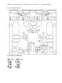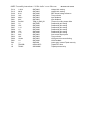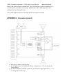
1
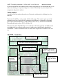
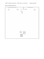
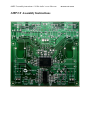
AMP2-T assembly instructions. © 41Hz Audio / www.41hz.com
AMP2-T Assembly Instructions
Revision 1.0T boards
AMP2-T assembly instructions. © 41Hz Audio / www.41hz.com
Revision 1.0T boards
TABLE OF CONTENT
Assembly instructions for AMP2.................................................................................................... 3
Considerations before you start .................................................................................................. 3
Tools needed ............................................................................................................................... 4
The PCB, a summary .................................................................................................................. 4
Components not included in the kit ............................................................................................ 6
Mounting the components........................................................................................................... 7
Trimming and testing................................................................................................................ 10
APPENDIX 1: Bill Of Materials (BOM) ..................................................................................... 16
BOM by component symbol / component name .......................................................................... 17
APPENDIX 2: Fine tuning the AMP2.......................................................................................... 20
Input impedance, input gain...................................................................................................... 20
Input capacitors......................................................................................................................... 21
Modulator gain.......................................................................................................................... 22
Current limiting......................................................................................................................... 22
Voltage limiting ........................................................................................................................ 23
APPENDIX 3: Mounting the TP2350B chip................................................................................ 24
Soldering the heat slug.............................................................................................................. 24
APPENDIX 4: Connector Pinouts ................................................................................................ 25
APPENDIX 5: Power supply board for the AMP2 amplifier....................................................... 25
The AMP2-T is an advanced high power amplifier. Building this amplifier is not for “beginners”.
It is assumed that you have thorough knowledge about electronics and building electrical and
electronic devices.
WARNING: The voltages and currents involved can be lethal if not handled properly. If you do
not have sufficient knowledge, do not proceed in building and using this kit. 41hz Audio can in
no way be held responsible for the consequences of the use of the kit.
AMP2-T assembly instructions. © 41Hz Audio / www.41hz.com
Revision 1.0T boards
Assembly instructions for AMP2
Thank you for choosing an audio kit from 41hz.com!
On delivery, check that all components have been included. If something is missing, let us know
immediately. A bill of material (BOM) should have been included with your delivery and is also
included here, as APPENDIX 1
Download the data sheet for the Tripath TK2350 reference board, as the schematic and layout of
AMP2-T is identical. However, component specifications and values may differ. Generally,
better components are delivered with the AMP2T kit than specified for the reference board. The
data sheet for the TK2350 is another useful source of information.
Considerations before you start
The AMP2 kit is designed for certain operating conditions. Depending on the way you will use
it, there will some considerations are left to you. The AMP2 kit is intended for supply voltages of
about +/- 40V to +/- 50V and four ohm or eight ohm speaker loads. With eight ohm loads, +/60V supplies can be used, with only minor changes. Power supply voltages or impedances
outside this range may require changing of some components. If you want to use the AMP2
board with 4 ohm loads and voltages higher than +/-50 and thereby very high power outputs, you
may also need to update some components. Also for lower voltages, you should change a few
component values. With the supplied components you will have the following:
- Current limiting is set to 10A. You may want to increase or decrease this depending on
your application.
- Voltage limiting is set to about +/-33 to +/-70 V. You may want to change this. Note that
supply voltages between +/-40 to +/- 60V are still recommended with the components in
the AMP2 kit.
- Input sensitivity. With the supplied components the amplifier is optimized for a nominal
average signal of 1.23V RMS at full power. This is the standard signal level for most pro
audio equipment and some HiFi preamplifiers. Domestic audio devices and portable
players without a preamplifier typically have a lower signal level and for those, a higher
input sensitivity setting in AMP2 may be required.
- Modulator gain (power stage gain) is selected so that the amplifier will start clipping at
2V RMS signal input with a +/-45V supply and the suggested input sensitivity. You may
want to fine tune this.
Please read more about how to fine tune the AMP2 kit in APPENDIX 2.
The driver chip TP2350B will dissipate some heat and must be kept cool. The board has
mounting holes for mounting a small heat sink over the chip. The bottom of the chip has a heat
slug. Heat transfer from the slug can be enhanced by heat transfer paste or by soldering the slug
to the board.
AMP2-T assembly instructions. © 41Hz Audio / www.41hz.com
Revision 1.0T boards
If you are not familiar with soldering surface mount components, it is recommended that you do
some test soldering on a separate scrap piece of material. Preferably buy some simpler kit or
components and practice on these.
Tools needed
Assembly of the kits requires the usual set of electronics working tools; soldering iron, wire
cutter etc.
The boards for AMP2 are triple weight, double sided copper. This requires quite a powerful
soldering iron to heat. Especially the components and pads that are connected to the ground
plane require substantial heating. A 50W soldering iron is the very minimum recommended.
Preheating the board to about 100ºC will help a lot.
If the heat slug of the TP2350B chip is to be soldered to the board (typically for AMPs used at
very high power) you will also need access to a solder oven or similar (more about this in
APPENDIX 3). Some information on how to solder SMT components is available on the web
site.
The PCB, a summary
5. Power MOSFETs
3. Gate drive resistors & current sensing
4. Power supply rail
2. MOSFET driver with
current / voltage sensing
6. Left channel
output and
output filters
7. Right channel
output and output
filters
1. Analogue input section
AMP2-T assembly instructions. © 41Hz Audio / www.41hz.com
Revision 1.0T boards
Figure 1: Top view of the PCB
The numbers refer to the sections shown in
Figure 1: Top view of the PCB.
1. The main component of the input section is one of the two chips in the TK2350 chipset;
the TC2001 signal modulator. This chip sees only low voltages 0 and +5V. It translates
analogue inputs to a digital signal train. Input and feedback resistors set the gain of the
input operational amplifiers in the TC2001 chip. Input capacitors block DC signal to and
from the chip. There are also offset trimmers and timing jumpers here. There are
connectors for low level signals to and from the board. The TC2001 chip modulator
generates binary logic level outputs that control the TP2350 MOSFET driver chip. The
driver frequency is 600 kHz at idle and is a spread spectrum type signal varying from
about 200 kHz to 1.2 MHz.
2. The TP2350B driver translates the logic signals from the modulator chip into level
shifted 10 volt high current pulses required to switch the power MOSFETs gates on and
off. The TP2350B chip also has voltage and current sensing inputs that can shut off the
gate drivers if the correct conditions are not met. The chip controls external power
MOSFETs. These are basically voltage controlled devices. But in reality, the gates of the
MOSFETs have a capacitance and a significant current pulse is required to switch the
MOSFETs on and off at high frequency. The TP2350 chip may get hot and therefore it
AMP2-T assembly instructions. © 41Hz Audio / www.41hz.com
Revision 1.0T boards
has a cooling slug that helps transporting heat to the PCB or a heat sink. There are
mounting holes through the PCB for optionally using an external heat sink on top of the
chip.
3. Gate drive resistors and protection diodes. These are between the driver chip and the
FETs and control the switching speed and indirectly also the heat dissipated by the driver
chip. Also, the current sense resistors are here.
4. This is the main power supply rail with positive, ground and negative supplies. The rail
has high ripple, low ESR, bulk capacitors that the MOSFETs draw current from. There
are also decoupling capacitors and protection diodes.
5. This is where the power switching MOSFETs are. There are normally two MOSFETS for
each side; one for the negative side and one for the positive side. Most users will
probably use only the standard MOSFETs. Each of the four FETs has a gate drive resistor
and protection diode. Between the power rail and the MOSFETs there are current sense
resistors for over current detection / protection. These shut down the output in case the
curret is too high, such as if the speaker cables are shorted (don’t try it…). The 10V
SMPS generator components are also located here. For the low side FETs, the gate drive
voltage must be 10V above the negative power rail. The TP2350B chip has a built in 10V
SMPS output that drives an external MOSFET and generates this voltage. The VN10
generator has its own inductor and capacitors to smooth out the ripple. Up to 200 mA
current is drawn from the negative rail for this.
6. Left channel output section. The output part for each side has filters that remove high
frequency patterns from the power switches that could otherwise recombine into audible
noise. A second order, two pole filter is used. It consists of a toroid inductor, some high
ripple filter capacitors and a snubber resistor. The corner frequency is in the order of 100
kHz. This section also holds the connection points for the loudspeaker leads.
7. The same as section 6 but for the right hand channel.
Components not included in the kit
The following parts / components will at some stage be needed to complete the amplifier, but is
not included in the kit:
-
Heat sink with screws and heat conductive paste to mount the heat sink. One of the great
advantages with PWM mode amplifiers is that the heat losses are small. However, this is
a high power amplifier and even if only a small percentage of the power is dissipated as
heat, the heat can be considerable for a high power / low impedance application.
-
Copper wire for the inductors. About 2.5 meters (8 ft) of 1.2 or 1.3 mm (AWG 16)
enamel insulation copper wire is needed. “Litz” type multi-strand wire of the same
equivalent area can also be used and is recommended as it is much easier to wind and has
good high frequency characteristics. However, Litz wire is expensive and a bit hard to
source.
AMP2-T assembly instructions. © 41Hz Audio / www.41hz.com
Revision 1.0T boards
-
Connection terminals and connection wire. I recommend soldering wires to the board
unless you plan to connect and disconnect them a lot. I also recommend you use the wire
you plan to use in your final application right from the start. The PCB leads and wire
required for connecting the power supply and speakers are heavy duty. Soldering them
requires substantial heat and with repeated soldering you risk damaging the PCB. There
is much debate in the audio world about connectors and IMO the best connector is none
at all; a well made solder connection is better than the best connector. Unless you need to
disconnect them frequently.
-
Wire jumpers. Depending on how you configure the board you will need some wire
jumpers.
Mounting the components
1. First, decide how to solder the TP2350B chip. If you are soldering the heat slug to the
board this must be done first, or at the same time as soldering the other components in an
oven. You should read more in APPENDIX 3 about this.
2. Solder all surface mount components on the bottom side. A picture of how the
components are placed is included below in Figure 2: Components, bottom view.
3. Mount the axial lead diodes D12, D22, D23, and D24 on the bottom side. Cut the leads
snugly on the top side of the board (and always do the final soldering after cutting the
wires).
4. Turn the board over and solder all surface mount components on the top side. A picture
of the component placement can be found in Figure 3: Components top view. The
component numbers are better seen in this figure than on the board. Most surface mount
components are placed around the U2 chip. Four diodes and four 0.1 uF decoupling
capacitors are placed above the U1 chip.
a. J1 is a jumper wires that set the BBM (Break Before Make) timing. Normally set
the BBM to 80 nS by placing the jumpers as shown in Figure 4. Shorter BBM
timing may cause current shoot-trough and is not recommended. 120 nS BBM
timing can be used for heavy duty (woofer amps) for increased shoot through
margin but may increase distortion in the > 2 kHz range.
b. Leave R33 open. It’s connected to an undocumented test pin. Tripath just state it
should be left open.
5. Solder the L3 inductor bead. This component connects the analogue signal ground plane
around the TC2001 chip to the rail power ground plane and dampens HF power ground
plane fluctuations from disturbing the analogue section.
6. Solder the axial resistors and diodes.
a. R31 and R32 are placed vertically, with one lead doubling back.
AMP2-T assembly instructions. © 41Hz Audio / www.41hz.com
Revision 1.0T boards
b. The leads of the current sense resistors R1, R2, R15, and R18. These should
preferably be mounted with some standoff that helps keeping them cool. The
whole supply rail current will pass through these resistors.
c. Mount the gate diodes and resistors D1, D2, D3, D4, R3, R4, R11 and R12.
d. Mount the other axial resistors.
7. Solder the offset trim potentiometers R104 and R204
8. Before connecting the final components, now is the time do a first test of the board. Do
not proceed further until the test described below, has completed successfully. Please
look at APPENDIX 4 for the connector pin assignments. Testing:
a. Check the resistance on the power supply connector J1. It should be about 1
Mohm between positive and ground, about 1.3 Mohm between negative and
ground and about 2 Mohm between positive and negative rail.
b. The +5V input should measure something like 0.5 kohm to ground.
c. The +5V supply should be well stabilized and fused, (before the voltage
regulator), at 200mA. Use a shielded cable for connecting the +5V and connect +
to pin 8 and negative to pin 7 of J2. The +5 supply should never go above +6V,
or be connected with wrong polarity, as this will damage the Tripath chipset.
Do not turn on the power yet.
i. Note, the +5V is used for both the analogue preamp section of the Tripath
chip and also for the logic level signals in the chipset. It is essential that
the +5V supply is quiet / well stabilized. Using shielded cable for hooking
up the +5V prevents feedback of high frequency EMI from the power amp
into the analogue section.
d. Connect the rail positive, ground and negative leads to J1. Double check the
polarity! Connecting the wrong polarity will damage components. The amp
may draw around 100 mA on the positive rail and around 200-250 mA on the
negative rail at “transistor radio volume”. Do not turn on the power yet.
i. As a protection you should use current limiting resistors in series with the
power supply lines. If the amp draws unexpectedly high current, the
voltage will drop below the level where under-voltage limit shuts off the
amp. Suitable resistor values can be 68 to 100 ohms, 3W for the positive
rail and 33 ohms to 47 ohm 3W for the negative rail. With the default
components, the amp will mute if the supply voltage drops below about
+/- 34V. Do not turn on the power yet.
ii. Alternatively, the amp could be protected with a 100mA fuse, placed on
the AC side of the supply. This way, both rails de-power in the case of
failure. The down side is that the energy in the supply capacitors may
discharge through the amp, even if the fuse has blown. Other fuse values
may be required, depending on your transformer and capacitors. Do not
turn on the power yet.
e. The onboard LED is connected via R90 (2.2K). Optionally, instead connect an
external LED from pin HMUTE (J2 pin 9), for example on the front panel of your
amp. An external LED needs its own 2.2 kΩ resistor to ground. A LED helps a lot
when testing.
i. Do not connect two LEDs at the same time, as this may draw too much
current from the HMUTE output
AMP2-T assembly instructions. © 41Hz Audio / www.41hz.com
f.
g.
h.
i.
j.
k.
Revision 1.0T boards
ii. The HMUTE output can be used to control speaker output relay, via a
driver circuit. The HMUTE will go high (+5V) in case the amp is muted
or in case of over current, over/under voltage and other errors. Shorted
outputs or shorted output transistors would also trig the over current
sensing. If no errors are detected and the amp is unmated HMUTE will be
low (0V).
Connect the MUTE input (J2 pin 11) to +5V (J2 pin 8) in a manner that the
MUTE signal can be shifted from +5V to ground (J2 pin 5, 6 or 7).
Switch on the +5V supply, but not the main rail voltage yet. The +5V should
draw about 25 mA. If a LED is connected to J2 pin 9, it should light up. If a LED
is not connected, check if there is +5V on the J2 pin 9.
Now, switch on the rail (main) power supply. It should draw a current of about
1mA.
Shifting the MUTE input from +5V to ground will toggle the amplifier from mute
to active. Now the amps should go active, and the +5V should draw about 50mA
and the LED (or J2 pin 9) should go low/off. If it does not, this indicates the
amplifier is still muted, for example because the voltage is too low or high or
current is over limits (shorted outputs…) If this happens, shut off the power,
dischargen the rail capacitors with a suitable resistor. Check all soldering and
everything else in the previous paragraphs. Do not proceed further until this
testing stage has passed successfully.
i. Note that under-voltage protection has a 200 mS delay and is non-latching
and the amp may “instantly” turn on again when the voltage recovers, and
then go on-off-on-off several times per second. In that case, turn the power
off!
ii. Note with the supplied voltage sense resistors, R112, R113, R114 and
R115, the lowest voltage the amplifier can be operated at is about +/-34V.
At lower voltages, the amp will not leave the mute state.
iii. Note also that the current sense (0.01 ohm) resistors must be in place for
this test to work.
When the amplifier is un-muted (LED is turned off), the positive rail should draw
a maximum of 40-80mA. The negative rail current may be 150-200 mA.
If everything looks OK, then power down, remove the current limiting resistors,
and proceed as described below.
9. Mount and solder film and ceramic radial lead capacitors.
a. There are two types of 0.1uF 250V film capacitors. C3 and C4 are rail to rail
mounted to reduce ripple on the DC supplies. These are Panasonic polyester caps
in a brownish dipped casing. C8 and C10 are part of the output filter and remove
high frequency ripple from the speaker outputs. A 100V rating would be
sufficient here but the 250V give a higher high frequency ripple voltage margin.
b. There are also four 100V 0.1 uF decoupling capacitors on the power rail; C1, C2,
C11 and C12.
10. Mount and electrolytic capacitors. Respect the polarity as marked on the PCBs.
a. There are two high ripple, low ESR bulk capacitors; C29 and C30. One on each
rail to ground and rated 100V. The C6 and C7 are rail to rail and therefore rated
160V.
b. C100 and C200 are the input capacitors. There are 1uF electrolytic Panasonic FC
capacitors are supplied in the kit. These are good quality standard capacitors.
AMP2-T assembly instructions. © 41Hz Audio / www.41hz.com
Revision 1.0T boards
c. There are three low ESR 100uF (150 uF) 35V for the onboard V10 PWM supply.
These are the C300, C19 and C71.
d. There are two 47uF for the bootstrap circuitry, C17 and C18.
11. Solder the inductor L4 and the Q1 MOSFET for the V10 supply.
12. Wind the toroid inductors. You should use 29 turns of 1.2 or 1.3 mm enamel insulated
wire for the T108-2 toroids included in the kit. The inductance should be 11 uH. Wind as
tight as you can. Tight winding minimizes any stray signals. This thick wire is a
challenge to wind. Leave a bit of wire so you can pull the toroids snugly to the board.
i. For high frequency, high current windings like the main inductors, a good
alternative is to use several thinner wires, with the same cross section area,
in parallel. A bundle of thin wires is easy to wind and the insulation
between strands reduces the “skin effect” and thereby reduces losses. You
can buy “Litz” wire which is simply a pre-made multi-strand wire, where
each strand is separately insulated with enamel insulation.
13. Scrape the enamel off the wires where they will be soldered and solder the wires to the
PCB. It may be a good idea to glue the toroids to the PCB to prevent the copper wires to
break from fatigue in case the PCB is subjected to vibrations. Use a temperature resistant
glue as the toroid will be warm at high loads.
14. Optionally solder board connectors ***J1 for power and J5 and J6 for speakers.
Connectors should have a current rating exceeding the currents you expect to have and
also exceed the current limit setting you use. The default for the AMP2 kits is 10A. If you
do not use connectors, solder the power cabling and speaker output cabling in place.
15. Connect signal connectors. Again consult the APPENDIX 4 and decide what connections
you would like to make.
a. Bridging or no bridging? Permanent bridging or an external switch?
b. Mute switch? Strongly recommended! If you do not use a switch, you should
permanently ground pin 11 of J2
c. Hmute indicator? The Hmute (pin 9 of J2) can drive an external LED via a 2 kΩ
resistor. The LED will be on if the amplifier is muted by pin 11 or due to over
voltage or over current limit has been exceeded.
16. Mount the four MOSFETs in positions M1, M2, M3 and M4. IMPORTANT. Take care
that the leads of the MOSFETS do not touch adjoining tracks before soldering them. The
legs of the provided MOSFETs have a fairly wide shoulder that may short circuit to
adjoining tracks. Therefore the MOSFETs should be lifted by about a millimeter before
they are soldered. Make sure they are in line, at the same height and flatly on the same
surface. They need to adhere well to the heat sink.
17. You are now ready to test the amplifier as described below. A heat sink is not required
for low power testing but will surely be required for higher power levels.
Trimming and testing
-
Put the amplifier to Mute (J2 pin 11 to pin 8)
AMP2-T assembly instructions. © 41Hz Audio / www.41hz.com
-
-
-
-
Revision 1.0T boards
Ground the signal inputs to signal ground (connect IN1 and IN2 to AGND on connector
J2). Do NOT connect the speakers yet.
Connect the +5V supply and its ground. A 100 mA fast fuse is recommended. Important;
If the +5V supply is higher than 6V the chipset will be permanently damaged. The 5V
supply should be well stabilized and filtered. A good option is to use a type 8705 with a
1000 uF before and another 1000 uF after the regulator. Voltage regulators should always
be bypassed with a 0.1 uF or similar at input and output, close to the chip. The regulator
data sheets usually give suggested schematics for this.
Connect the power supply. Double check the polarity of the power supply. Wrong
polarity will permanently destroy some components, including the Tripath chipset. For
the first testing, use current limiting resistors as described above.
Turn on the power.
When muted and with no speakers connected, the +5V should draw about 20 mA and
each main rail should draw about 1mA.
Switch the MUTE setting from Mute to Awake
Check the fuses. If they have blown, disconnect the board and check all components and
solders.
With the amp unmated (awake) the +5V should draw about 50mA and the positive rail
should draw about 80mA, the negative about 200 mA.
If the fuses are OK then, adjust the trimmer pots until the speaker output signal is as close
to 0V as you can get it. This minimizes turn on/off pops and minimizes DC through the
speakers. You should be able to trim the offset to below 10 mV. Do not run the amp for
extended periods without speakers or a dummy resistor connected.
Shut of the power.
Connect the speaker wires
Connect a signal source with music.
Set the volume on the signal source very low
Turn on the power and check if you get any sound.
If everything seems OK, switch off power, replace the power supply fuses for larger fuses
like 1A and try again at slightly higher volume. (The 5V fuse should remain about 100200mA).
For testing at low power no heat sink is required. For low to medium power applications
the amplifier housing may be sufficient as a heat sink. For high power outputs, you
should have an efficiency of 90-95% with 8 ohm loads and 85-90% with 4 ohm loads.
The rest of the power, 5-15%, can be assumed that is dissipated from the MOSFETs. I.e.
if you drive the amplifier to 2x150W into 8 ohms you will have 15-30W of heat
dissipated. If you drive the amp to 2x300W into 4 ohms you will have 60-90W of heat.
Select a heat sink / cooling method that can handle this. Keeping the FET temperature
down is important for reliability and lifetime. The MOSFETs must be electrically
insulated form the heat sink. Using thick pads between the FETs and heat sink is a good
idea s this decreases capacitive coupling between FETs and heat sink, and thereby
minimizes the EMI that may otherwise be emitted by the heat sink.
Connect the amplifier to your power supply and change the power supply fuses to the
proper value.
Enjoy!
Please note:
• Speaker leads must be grounded to the PCB connectors, not to the power supply.
The modulator feedback has separate returns from these connections. The
speaker returns are grounded in a star point on the PCB.
AMP2-T assembly instructions. © 41Hz Audio / www.41hz.com
•
Revision 1.0T boards
Audio signal sources and the 5V supply must be grounded to J2. This connector
is in turn connected via an inductor bead to the star grounding point where the
power supply is connected.
If you have any questions, write any questions on the forum on our web site
http://www.support.41hz.com , as the questions may be of general interest.
For any questions please do not hesitate to contact us at [email protected]
Feedback is very much appreciated!
AMP2-T assembly instructions. © 41Hz Audio / www.41hz.com
Figure 2: Components, bottom view
Revision 1.0T boards
AMP2-T assembly instructions. © 41Hz Audio / www.41hz.com
Figure 3: Components top view
Figure 4: Jumper J1 BBM settings
Revision 1.0T boards
AMP2-T assembly instructions. © 41Hz Audio / www.41hz.com
Figure 5: Shape of current sense resistors
Revision 1.0T boards
AMP2-T assembly instructions. © 41Hz Audio / www.41hz.com
APPENDIX 1: Bill Of Materials (BOM) ***
Count
(R) 4
(C) 11
(C) 4
(C) 2
(C) 2
(C) 2
(R) 4
(R) 1
(R) 9
(C) 2
(R) 4
(R) 1
(R) 2
(R) 1
(R) 6
(R) 4
(R) 5
(R) 2
(C) 2
(C) 2
(R) 2
(C) 1
(C) 1
(C) 3
(L) 1
(C) 1
(C) 2
(R) 2
(C) 2
(C) 2
(C) 1
(C) 4
(R) 1
(R) 2
(R) 4
(L) 1
(Q) 1
(M) 4
(D) 8
(D) 6
(R) 2
(D) 1
(U) 1
(L) 2
(U) 1
(Board) 1
Value
0.01 ohm
0.1 uF 50V
0.1 uF 100V ceramic
0.1 uF 100V (250V)
0.1 uF 250V
0.22 uF 100V (250V)
1.1 K
1.18 M
1K
1 uF 10V (63V)
2.2 ohm 1W
8.2 K
10 K
10 ohm
15 ohm 1W
15 K
20 K
22 ohm 3W
33 pF 50V
47 uF 25V
49.9 k
100 pF 50V
100 uF 10V
100 uF 35V low ESR
100 uH 2A inductor
150 pF 50V
33 uF 160V Low ESR, high ripple
220 ohm 0.25W
220 pF 50V (200V)
220 pF 200V
270 pF 50V
220 uF 100V Low ESR, high ripple
392 K
422 K
510 K
Ferrite bead
IRF9510 or MTP12P10
MOSFET STW34NB20
MUR120 diode, ultra fast
MURS120 diode, ultra fast
Pot 50K
Schottky 1A 35V
TC2001
Toroid (11uH)
TP2350B
AMP2 PCB
Package
Axial 1% 2W
SMT 0805
Radial
Radial
Radial
Radial
SMT 0805
SMT 0805
SMT 0805
Radial
Axial
SMT 0805
SMT 0805
SMT 0805
Axial
SMT 0805
SMT 0805
Axial
SMT 0805
Radial
SMT 0805
SMT 0805
Radial
Radial
Radial
SMT 0805
Radial
Axial
SMT 0805
SMT 0805
SMT 0805
Radial
SMT 0805
SMT 0805
SMT 0805
Axial
TO220
TO247
Axial
SMB
Trimmer
SMB
SOIC28MIC
Toroiod for winding, T106-2
64PIN-LQFP
Revision 1.0T boards
AMP2-T assembly instructions. © 41Hz Audio / www.41hz.com
Revision 1.0T boards
BOM by component symbol / component name
Symbol
C1
C2
C3
C4
C5
C6
C7
C8
C9
C10
C11
C12
C13
C14
C15
C16
C17
C18
C19
C20
C27
C29
C30
C31
C32
C35
C40
C5A1
C60
C71
C100
C103
C107
C200
C101
C201
C203
C207
C300
C301
C332
D1
D2
D3
D4
D5
D6
D7
Value
0.1 uF 100V
0.1 uF 100V
0.1 uF 250V
0.1 uF 250V
0.22 uF 100V
33 uF 160V
33 uF 160V
0.22 uF 100V
0.22 uF 100V
0.22 uF 100V
0.1 uF 100V
0.1 uF 100V
0.1 uF 50V
0.1 uF 50V
0.1 uF 50V
0.1 uF 50V
47 uF 25V
47 uF 25V
100 uF 35V
0.1 uF 50V
0.1 uF 50V
330 uF 100V
330 uF 100V
220 pF 200V
220 pF 200V
0.1 uF 50V
0.1 uF 50V
0.1 uF 50V
100 pF 50V
100 uF 35V
1 uF 10V
220 pF 50V
270 pF 50V
1 uF 10V
33 pF 50V
33 pF 50V
220 pF 50V
150 pF 50V
100 uF 35V
0.1 uF 50V
0.1 uF 50V
MUR120
MUR120
MUR120
MUR120
MURS120
MURS120
MURS120
Footprint
CAP_RM5_7.2X2.5
CAP_RM5_7.2X2.5
CAP_RM7.5_10X6
CAP_RM7.5_10X6
CAP_RM15_20X7
CAP RADIAL
CAP RADIAL
CAP_RM15_20X7
CAP_RM15_20X7
CAP_RM15_20X7
CAP_RM5_7.2X2.5
CAP_RM5_7.2X2.5
SMT 1206
SMT 1206
SMT 0805
SMT 0805
CAP6MM_RAD_RM2.5
CAP6MM_RAD_RM2.5
CAP8MM_RAD_RM3.5
SMT 0805
SMT 0805
CAP RADIAL
CAP RADIAL
SMT 0805
SMT 0805
SMT 0805
SMT 0805
SMT 0805
SMT 0805
CAP8MM_RAD_RM3.5
CAP_RM15_20X7
SMT 0805
SMT 0805
CAP_RM15_20X7
SMT 0805
SMT 0805
SMT 0805
SMT 0805
CAP8MM_RAD_RM3.5
SMT 0805
SMT 0805
MUR_RM10
MUR_RM10
MUR_RM10
MUR_RM10
SMB_DIODE
SMB_DIODE
SMB_DIODE
Comment
Rail decoupling
Rail decoupling
Rail-Rail decoupling
Rail-Rail decoupling
Output filter
Rail-rail power supply decoupling
Rail-rail power supply decoupling
Output filter
Output filter
Output filter
Rail decoupling
Rail decoupling
Decoupling of feedback
Decoupling of feedback
Decoupling of boot circuit
Decoupling of boot circuit
Boot circuit cap
Boot circuit cap
VN10 decoupling
Decoupling of VN10
Decoupling of VN10 SMPS feedback
Power supply close-up buffering
Power supply close-up buffering
Output snubber
Output snubber
Decoupling of V5
Biascap
Decoupling of VN10
Decoupling of VREF
VN10 decoupling
Input capacitor
Current set point delay
Feedback delay / switch frequency
Input capacitor
Input RF decoupling
Input RF decoupling
Current set point delay
Feedback delay / switch frequency
VN10 decoupling
Decoupling of VN10
Decoupling of V5
Gate discharge diode
Gate discharge diode
Gate discharge diode
Gate discharge diode
Boot diode
Boot diode
Protection of HF feedback
AMP2-T assembly instructions. © 41Hz Audio / www.41hz.com
D8
D9
D10
D11
D21
D22
D23
D24
L1
L2
L3 (FB)
L10
M1
M2
M3
M4
Q1
R1
R11
R2
R12
R3
R4
R5
R6
R7
R8
R9
R10
R13
R14
R15
R16
R17
R18
R19
R20
R22
R30
R31
R32
R100
R101
R104
R105
R106
R107
R108
R109
R110
R111
R112
R113
MURS120
MURS120
MURS120
Schottky 1A 100V
MUR120
MUR120
MUR120
MUR120
Toroid 11uH
Toroid 11uH
Ferrite bead
100 uH
MOSFET
MOSFET
MOSFET
MOSFET
IRF9510
0.01 ohm
15 ohm
0.01 ohm
15 ohm
15 ohm
15 ohm
510 K
510 K
2.2 ohm
2.2 ohm
22 ohm
22 ohm
510 K
510 K
0.01 ohm
2.2 ohm
2.2 ohm
0.01 ohm
220 ohm
220 ohm
20 K
2.2 K
15 ohm
15 ohm
49.9 k
20 K
Pot 50K
1K
15 K
1.1 K
1K
15 K
1.1 K
20 K
422 K
422 K
SMB_DIODE
SMB_DIODE
SMB_DIODE
SMB_DIODE
MUR_RM30
MUR_RM10
MUR_RM10
MUR_RM10
T108-2
T108-2
R05W
Inductor
TO220 or TO248
TO220 or TO248
TO220 or TO248
TO220 or TO248
TO220
R2W Ohmite axial 1%
R1W
R2W Ohmite axial 1%
R1W
R1W
R1W
SMT 0805
SMT 0805
R1W
R1W
R3W
R3W
SMT 0805
SMT 0805
R2W Ohmite axial 1%
R1W
R1W
R2W Ohmite axial 1%
R05W
R05W
SMT 0805
SMT 0805
R1W (vertical)
R1W (vertical)
SMT 0805
SMT 0805
TRIM_3_RM5_D6
SMT 0805
SMT 0805
SMT 0805
SMT 0805
SMT 0805
SMT 0805
SMT 0805
SMT 0805
SMT 0805
Revision 1.0T boards
Protection of HF feedback
Protection of HF feedback
Protection of HF feedback
VN10 SMPS diode
Overshoot protection of outputs
Overshoot protection of outputs
Overshoot protection of outputs
Overshoot protection of outputs
Output filter inductor
Output filter inductor
EMI damping analog ground Ù ground
VN10 SMPS inductor
Main FET
Main FET
Main FET
Main FET
VN10 FET
Current sensing
Gate drive current limiting
Current sensing
Gate drive current limiting
Gate drive current limiting
Gate drive current limiting
Gate ground reference
Gate ground reference
Feedback damping
Feedback damping
Output zobel filter
Output zobel filter
Gate ground reference
Gate ground reference
Current sensing
Feedback damping
Feedback damping
Current sensing
Boot circuit current limiting
Boot circuit current limiting
Bridging resistor
LED current limiting
FET snubber
FET snubber
Input feedback
Input feedback
Trimmer for nulling output offset
Feedback & gain setting
Feedback & gain setting
Feedback & gain setting
Feedback & gain setting
Feedback & gain setting
Feedback & gain setting
Over-current trip set point
Voltage limit sensing
Voltage limit sensing
AMP2-T assembly instructions. © 41Hz Audio / www.41hz.com
R114
R115
R120
R122
R200
R201
R204
R205
R206
R207
R208
R209
R210
R211
R222
R300
R301
R33
U1
U2
1.18 M
392 K
8.2 K
10 K
49.9 k
20 K
Pot 50K
1K
15 K
1.1 K
1K
15 K
1.1 K
20 K
10 K
10 ohm
1K
----TP2350B
TC2001
SMT 0805
SMT 0805
SMT 0805
SMT 0805
SMT 0805
SMT 0805
TRIM_3_RM5_D6
SMT 0805
SMT 0805
SMT 0805
SMT 0805
SMT 0805
SMT 0805
SMT 0805
SMT 0805
SMT 0805
SMT 0805
SMT0805
64PIN-LQFP
SOIC28MIC
Revision 1.0T boards
Voltage limit sensing
Voltage limit sensing
REF internal voltage reference
Trim pot limiter
Input feedback
Input feedback
Trimmer for nulling output offset
Feedback & gain setting
Feedback & gain setting
Feedback & gain setting
Feedback & gain setting
Feedback & gain setting
Feedback & gain setting
Over-current trip set point
Trim pot limiter
VN10 gate drive current limiting
VN10 feedback
Leave open. Internal Tripath test only.
Tripath FET driver
Tripath processor chip
AMP2-T assembly instructions. © 41Hz Audio / www.41hz.com
Revision 1.0T boards
APPENDIX 2: Fine tuning the AMP2
The components included in the AMP2 kit work well for many users. For optimal performance
the AMP2 board may be fine tuned to each application. Here is a summary of what to think of.
Input impedance, input gain
The TK2350 can be described as a two stage amplifier. The first is an operational amplifier while
the second is the power stage / modulator.
So first we have to select input and gain resistors for the input operational amplifier. The input
impedance has an effect on any equipment upstream of the amplifier, such as pre amplifiers.
Modern pre-amplifiers are usually capable of driving fairly high currents / low impedance loads.
But usually, the THD+N is better if the impedance is not to low. On the other hand very high
impedance in the power amplifier will introduce current noise so a compromise has to be found.
Values of between 10k Ω and 100KΩ are typical while 20 KΩ to 50 KΩ are most common.
Some people prefer carbon thick film resistors for the input and feedback resistors while others
prefer thin film or metal film resistors which usually have lower noise. With thick film carbon
resistors we could use lower values, say 20 KΩ for low noise while higher values can be used
with thin film or metal film, often 50 KΩ.
Most consumer audio equipment like CD players etc have a signal level output of -10dBV which
corresponds to 0.316 V RMS. Portable devices like MP3 players, MD and CD players often
have lower output to extend battery life. A preamplifier would usually have a gain of about +10
dB giving an output of 0dBV or 0.775 V RMS maximum. Similar levels could be expected from
computer soundcards. Professional equipment usually has a nominal +4 dBU maximum output
signal which corresponds to 1.23 V RMS.
The TK2350 amplifier chip modulator stage has a maximum input level of about 4V peak to
peak, equivalent to 1.41 V RMS. For best performance we should select the gain for the input
stage so that at maximum volume (from the preamp) the voltage in the input stage is close to the
maximum 4Vptp. Some headroom margin for transient peaks is however required.
The following table gives some examples. For a consumer audio level signal of 0.316 V and
select a gain of one (1) for the power amplifier input stage, we would have headroom of 15dB
which is a bit much and means the amplifier can not reach its maximum power. If we add a
+10dB gain preamplifier we would have headroom of 5 dB which is reasonable. With a pro
audio input of 1.23 V and an amplifier gain setting of -0.4 we would have 10dB headroom,
which again is reasonable.
AMP2-T assembly instructions. © 41Hz Audio / www.41hz.com
Revision 1.0T boards
Consumer
audio
With +10 dB
pre-amp
Pro audio
+4dBU
Value in
AMP2 kit
Nominal VinRMS
AMP2 Gain
Rin
Rfeedback
0.316
1
50 KΩ
50 KΩ
0.775
1
50 KΩ
50 KΩ
1.23
0.4
50 KΩ
20 KΩ
1.23
0.4
50 KΩ
20 KΩ
Headroom/margin
15 dB
5 dB
10 dB
Component in
AMP2
R100, R200
R101, R201,
(& R99 for bridging)
The gain, G is calculated: G = -Rfeedback/Rin
The AMP2 kit is shipped with 50 KΩ input resistors and 20 KΩ feedback resistors for
a 0.4 gain. These are 0805 size low noise thin film type. You may want to adjust these values for
your own application. On request we can supply other resistor values than the ones included.
SUMMARY
• The input sensitivity with the AMP2 kit components are suitable for a pro audio signal
level of 1.23VRMS (+4 dBu)
• For home audio equipment you should probably increase the input stage gain by
replacing the 20 K feedback resistors with other, higher values.
Input capacitors
Some people have an almost religious in the belief of the influence on the sound quality from the
input capacitors. The AMP2 PCBs have space for RM5, RM10 and RM15 lead spacing for the
input capacitors so you can practice your belief. You can use many different types of
capacitors. Input capacitors are recommended as they block any DC from flowing between
equipment components. The inputs of the Tripath chips are biased by about 2.5V, so a capacitor
is usually required. However, if you hardwire the power amp to a preamplifier that has a
capacitor on the output, then the input capacitor to the power amplifier can be omitted and
replaced by a jumper. The input impedance resistor and the input capacitor form a high pass
filter. The corner frequency is
fc = 1/(2*Pi*Rin*Cin).
The value should be chosen so that the corner frequency is well below the used lowest
frequency. There will be a phase shift close to the corner frequency so a margin of at leas one
octave is desirable. A fc of lower than 10 Hz should usually be used for full range and woofer
amplifiers. Higher values can be used for mid range / tweeter amplifiers. Sometimes it is claimed
that input capacitor values should be about 5 uF or more. This may be true with older carbon
film input resistors where impedance had to be low to minimize noise. But with low noise thin
film resistors, fairly high impedance can be used and a corresponding low value for the
capacitor. The AMP2 kit is shipped with 50 KΩ input resistors and 1 uF capacitors, giving a
corner frequency of 3.2 Hz.
It should be noted that two capacitors in series (in the pre amp output and power amp input) will
AMP2-T assembly instructions. © 41Hz Audio / www.41hz.com
Revision 1.0T boards
combine into half the equivalent value, increasing the corner frequency. It can also be noted that
the Tripath boards and measurement results given in the Tripath data sheets are usually done
with standard electrolyte capacitors as input caps.
Modulator gain
The AMP2 and TK2350 is a feedback topology. The voltage gain of the power section of the
amplifier is set by resistors that feed back the loudspeaker output voltage to the chipset. The
ground for each side has separate lead backs, for accurate sensing. This means there are four
feedback paths and four feedback resistors. For optimal amplifier use, the gain resistor values
could be changed, depending on the used rail voltage and the application. Some "over gain"
could be used so that the power stage will start clipping, i.e. output voltage is as high as the rail
voltage, when the input signal is a bit over the nominal maximum. If the gain is set to low then
the power stage will run below full power even when the input stage signal is high enough to
saturate the input stage. If the gain is to high, the power stage will start clipping at a low input
signal and this implies the preamp level has to be turned down, which may be unfavorable from a
THD+N point of view, especially at low volume. A reasonable balance has to be found.
Calculating the modulator gain / feedback resistor values
Description
Typical value
Vpp Rail voltage (+/-)
40-50V
50-60V
Rfba Typical value
1 KΩ
1 KΩ
Rfbb = Rfba * Vpp/(Vpp-4)
1.1 KΩ
1.07 KΩ
Rfbc = Rfba * Vpp/4
12 KΩ
15 K
AMP2 Component
R105, R108, R205, R208
R107, R110, R207, R210
R106, R109, R206, R209
Current limiting
The TK2350 chipset has built in over current setting. Actually, it senses the voltage over a
current sense resistor via set point resistors. The set point resistors are of the 0805 size. At an
over current situation the amplifier will go into mute and has to be power cycled off/on to reset.
The resistors supplied in the AMP2 component kit are 20 KΩ and will trip the amplifier at 10A.
You may want to select other values for your application. The on-board power supply capacitors
are placed after the current sense resistors. Therefore the MOSFETs may draw current from the
caps and the current sense resistors will see a slightly smoothed current signal. The over current
sensing is still fast and will mute the amplifier even on short over current peaks. Please note that
the over current shut-off sets the chipset into mute state but if the MOSFETs are damaged, the
rail voltage can still be on the speaker outputs. The over current protection should therefore be
regarded as “soft” protection. Proper fuses are still required. But fuses may not blow before the
loudspeakers are damaged. For “hard” shutdown you can use a relay on the speaker outputs,
controlled by the HMUTE signal output. This will shut of the speaker outputs even if the output
FETs are damaged.
AMP2-T assembly instructions. © 41Hz Audio / www.41hz.com
Revision 1.0T boards
Calculating the over current sense resistor values
Description
Current limit trip point
Component
6A
10A
12A
16A
22A
Isc
Over-current trip point
0.01
Ω
0.01
Ω
0.01Ω
0.01Ω
0.01Ω R51, R52, R53, R54
Rsense Current sense resistor
20K
18K
15K
12K
R111, R211
Rorc =3473/(Rsense* Isc+0.0716) 27K
Voltage limiting
The TK2350 chipset also has over / under voltage sensing. The voltage values are set with four
resistors in the 0805 size. If the voltage is outside the specified values, the amplifier will mute.
Unlike the over current sensing the voltage sensing is non latching i.e if the amplifier is unmuted it will mute when outside the specified range and go back to the un-muted state as soon as
the voltage is within specified values again. Please again note that that the over voltage sensing
sets the chipset in mute and can prevent damage by stopping instable conditions like power
supply transients. However it can not protect the chipset from severe over voltage damage; the
maximum chipset voltage is +/- 70V also when muted.
The voltage limiting trip point resistor values
Description
Vpp
Rail voltage (positive)
Vnn
Rail voltage (negative)
Ivppsense
Positive sense current from data sheet
Ivnnsense
Negative sense current from data sheet
Rvpp1
= Vpp / Ivppsense
Rvpp2
= Vpp / Ivppsense
Rvnn1
= Vnn / Ivnnsense
Rvnn2
= 3xRvnn1
Value in the AMP2 kit
(+40 to +60V)
(-40 to -60V)
(0.162mA)
(0.174mA)
422 KΩ
422 KΩ
392 KΩ
1.18 MΩ
Component in AMP2
R112
R113
R115
R114
The tolerances of the voltage sensing and limiting are not very tight so there may be variations in
the actual trip points. Please see the TK2350 chipset datasheet for details.
The resistors supplied with the AMP2 component kits will set the lower voltage limit to about
+/- 33 volts and the upper limit to about +/- 65 volts.
Note you should have a margin of about 5V from the nominal power supply voltage, or the
voltage protection may mute the amp due to voltage transients and component tolerances.
AMP2-T assembly instructions. © 41Hz Audio / www.41hz.com
Revision 1.0T boards
APPENDIX 3: Mounting the TP2350B chip
The TP2350B driver chip can produce some heat, especially if driving MOSFETs with high gate
charges and / or at high rail voltages. The chip has a slug on the bottom side that enhances the
heat transfer from the chip. The AMP2 PCB has a corresponding area with a number of holes /
vias that lead heat from the chip to the back of the PCB. There are also four larger mounting
holes around the chip so a heat sink can be mounted with screws on top of the chip. So to
enhance the heat transferal, it is possible to
- Use heat conductive paste on the bottom of the chip
- Solder the chip slug to the PCB.
- Use a heat sink on top of the chip and also under the chip.
It is recommended that at least one of these methods is used, especially at high power outputs
and high rail voltages.
The use of heat conductive paste on the bottom of the chip is probably the most straight forward
method and this method can be used for light and medium loaded amplifier boards. It also has
the advantage that it is possible to replace the chip without too much trouble. For higher power
applications, such as woofer amplifiers and highly loaded pro amplifiers it is recommended to
solder the slug to the PCB or / and use a heat sink.
Soldering the heat slug
The chip heat slug can not be soldered with a solder iron as it is at the bottom of the chip. A
solder oven or similar must be used. Even a domestic electric oven can be used if no solder oven
is available. Do as follows:
1. Make sure your solder material has a melting point that is not higher than 190 ºC. Most
60%Zn 40%Pb will melt at around 180ºC
2. Heat an oven to about 230-240 ºC
3. Scrape of the solder mask in the rectangle in the middle of the U1 chip position on the
PCB with a sharp knife. Make sure you remove all solder mask varnish in this area.
4. Place about 20 mm (3/4”) long bit of solder with a diameter of 0.6 mm or the equivalent
amount, bent into a circle, on the cleaned PCB area. Place the PCB in the oven and
measure the time it takes before the solder has melted and flowed out on the solder area.
It may take about 2-3 minutes.
5. Remove the PCB from the oven and let the PCB cool down.
6. Spread some “no-clean” non aggressive solder flux on the solder area. A solder flux pen
is handy for this.
7. Place the TP2350B chip perfectly in place on the PCB. Make sure all chip leads are
aligned to the solder pads of the PCB.
8. Place the PCB in the oven and allow as much time as before, but add 20 seconds for the
chip to heat up. After this time shut of the oven power, open the oven door and gently
fan cool air into the oven.
9. Let the PCB cool down and inspect it.
10. If everything is OK, solder the chip legs to the PCB pads.
AMP2-T assembly instructions. © 41Hz Audio / www.41hz.com
Revision 1.0T boards
Most Zn-PB solder will melt at around 180ºC. The TP2350B chip is tested for soldering for 10
seconds in 260ºC so you have some margin. Subjecting the chip to high temperatures for a
prolonged time may damage the chip.
The TC2001 chip does not have a heat slug and does not require a heat sink.
APPENDIX 4: Connector pinouts
•
•
•
Mute jumper; close to awake the amp
The V5-agnd must be well stabilized / filtered. Voltages above 5.5V will damage the
Tripath chipset
In1 and In2 should be grounded as indicated, not elsewhere. Input signals above +/- 2.5V
can damage the TC2001 chip.
AMP2-T assembly instructions. © 41Hz Audio / www.41hz.com
APPENDIX 5: Power supply board for the AMP2 amplifier
Coming…
Revision 1.0T boards
AMP2-T assembly instructions. © 41Hz Audio / www.41hz.com
APPENDIX 6 AMP2 Specifications
Coming…
Revision 1.0T boards