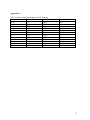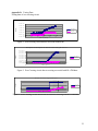
1
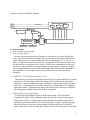
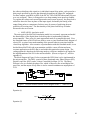
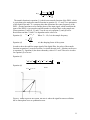
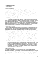
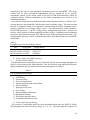
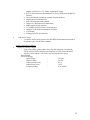
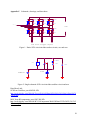
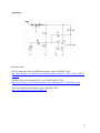
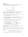
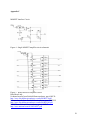
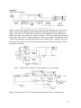
ECE 481 Senior Design Project Final Report
For
Scalable Regulated Three Phase Power Rectifier
December 10, 2004 Rev. 1.0
Sponsors: Dr. Herb Hess (University of Idaho)
Dr. Richard Wall (University of Idaho)
Instructor: Dr. Jim Frenzel (University of Idaho)
Prepared By,
Tao Nguyen
[email protected]
Tyler Budzianowski
[email protected]
2
II.
Table of Contents
Abstract………………………………………………………………………………………..5
Project Description
Problem Statement…………………………………………………………………….5
Solution Method………………………………………………………………………5
Project Status
What is designed and working
Zero crossing detector…………………………………………………………6
MOSFET 5V/12V interface circuit……………………………………………6
SCR rectifying circuit………………………………………………………....6
PIC16C74B microcontroller (open loop)…………………………………...…7
MATLAB simulation model…………………………………………………..7
What is designed but not working
PIC16C74B microcontroller (closed loop)……………………………………7
What is designed but not tested
Six SCR rectifier circuit……………………………………………………….7
Enerpro FCO-AUX60 firing circuit………………………………………...…7
Method of Solution
Technical description and theoretical basis
Zero crossing detector…………………………………………………………8
MOSFET 5V/12V interface circuit……………………………………………8
SCR rectifying circuit………………………………………………………....8
PIC16C74B microcontroller………………………………………………..…9
MATLAB simulation model……………………………………………..10, 11
Validation Procedure
Testing Method
Zero crossing detector……………………………………………………..…12
MOSFET 5V/12V interface circuit…………………………………....….….12
SCR rectifying circuit……………………………………………..………....12
PIC16C74B microcontroller…………………………………....……………13
3
MATLAB simulation model……………………………...… ………………13
Testing Results
Zero crossing detector……………………………….…………...………..…13
MOSFET 5V/12V interface circuit…………………………..….………..…13
SCR rectifying circuit……………………………………………...………...14
PIC16C74B microcontroller………………………………………..……..…14
MATLAB simulation model……………………………..…………….….…14
Manufacturing and Support
Product Life Cycle
Design and Development Phase……………………………………………...15
Introductory Phase………………………………………………………..….15
Active Phase………………………………………………...………….……15
Functionally Stable Phase………………………..……………………….…16
Maturity Phase………………………………………..……………….…….16
Retirement Phase………………………………………..…………………...17
Failure Modes, Effects, and Criticality Analysis (FMECA)
Overview…………………………………………………………………….17
FMECA ………….……………………………………………………….…18
Conclusion of FMECA…………………………………..…………...……...19
Societal Concerns…………………………………………….………………………20
Appendix
A Specifications…………………………………………………………………..…21-24
B. Bill of Materials…………………………………………………………………..….25
C. Schematics, Drawings, Data Sheets…………………………………………..….26-30
D. Test Data…………………………………………………………………...……..31-40
E. User Manual…………………………………………………..……...………………41
4
III.
Abstract
The scalable three phase rectifier project is based on an original 1996 design created by Dr.
Herb Hess and Dr. Richard Wall of the Electrical and Computer Engineering Department at
the University of Idaho. The original prototype utilized an Intel 80C196KD microcontroller
with a digital phase locked loop (PLL) and a three component design including the processor,
optoisolator zero crossing detectors, and SCR gate drivers. The original processor is no
longer available and newer hardware implementation methods have been discovered since
this inception. The new design for this project utilizes a modern, less expensive, and widely
available processor, as well as the newer and more accurate hardware implementation
methods (zero crossing, gate firing architecture, SCR snubbing and protection). This
implementation is described in detail in this technical document.
IV.
A. Project Description
i. Problem Statement
Due to the fact that new technologies have been recently developed to increase the accuracy
and efficiency of the microcontroller-based three phase rectifier system, changes need to be
made to the existing design to produce a product with the highest accuracy, reliability, and
reproducibility possible. The obsolescence of the Intel 87C196KD-20 microcontroller, zero
crossing detection methods, and hardware implementation methods included in the original
design brings the need for newer and more widely available replacement techniques. The
original design was also not easily understood nor reproducible by others seeking similar
results, creating the need for inexpensive and widely available commercial components in the
design as well as a phase locked loop software model.
ii. Solution Method
To apply the newer technologies and components now available, an upgrade to a Microchip
PIC16C74B microcontroller system was the starting point to replace the obsolete Intel
processor and has the adequate resources necessary to implement the 6 pulse firing and a
phase locked loop. To increase accuracy in the input AC line zero crossing detection, new
methods for zero-crossing detection as outlined in Richard Wall’s 2003 paper entitled
“Simple Methods for Zero Crossing Detection” were analyzed and applied to this design. It
was determined that replacing the original optoisolator zero crossing detection configuration
with a dynamic hysteresis comparator circuit would be most ideal. To further the accuracy in
this system, a phase locked loop implementation similar to the original design would need to
be employed. In following the need for commercially available components, an Enerpro
FCO-AUX60 SCR gate firing board was chosen to accurately and reliably amplify and relay
the firing signals (6 total) from the output of the microcontroller to the gates of the SCRs.
Using this device did require the need for an interface circuit between the PIC16C74B
processor (5 V logic) and the FCO-AUX60 board (12 V logic). The newer device needed to
employ methods of snubbing and protection for the SCRs as well. The application of these
newer components and techniques is the main purpose of the system design.
5
Overview of the System Block Diagram:
M
O
V
S C R
S n u b e r
C i r c u it
7 8 0 5
Z e r o C r o s s in g
C ic ru it
P o w e r
S u p p ly
L M 3 1 7
O
u
t
p
u
t
s
In p u ts
P IC
K E Y P A D
u C o n t r o lle r
C
M
O
S
In te r f a c e
C K T
G a te
F irin g C irc u it B o a r d
F C 0 -A U X 6 0
L C D
B. Project Status
i. What is designed and working
a. Zero Crossing Detector
The zero crossing detection circuit functions as designed but with some slight offset
error. The circuit can detect the rising edge zero cross point of the input sinusoidal line
signal, and convert it to a square digital logic pulse of magnitude 0 to 5 V. However,
there is a slight offset error in the actual zero crossing time of the sinusoidal signal, and
the detected zero crossing time of the circuit. This has been concluded to be due to the
resistance value between the comparator and the AC line interface, which is too high to
allow enough significant current to the dual schottky diode junction and to the input of
the comparator. A lower input resistor value causes this error to decrease and/or
disappear.
b. MOSFET 5V/12V firing board interface circuit
The transistor circuit that was designed to interface the 5V microcontroller logic output
signal to the 12V logic input signal of the Enerpro FCO-AUX60 gate firing board is
functional. Using a configuration of three MOSFET transistors per channel (6 channels
total), the 5 V input signal is successfully amplified to an identical but 12V magnitude
signal at the output. Switching times among the transistors have not been a problem in
the testing process and the subcircuit functions as designed.
c. SCR rectifying circuit (single stage)
A single stage representation of the six-SCR circuit design is fully functional.
Comprised of a single SCR, a snubbing resistor & capacitor, and a protection metal
oxide varistor (MOV), a voltage applied across the anode and cathode of the SCR is
successfully passed through the device when an adequate voltage is applied to the gate.
The device turns on with a gate voltage applied, produces a half-wave rectified DC
output, and turns off again once the gate voltage is removed and the input AC sinusoidal
6
signal crosses the zero point on its falling edge. The sinusoidal input AC signal is thus
rectified to a DC output value as was designed.
d. PIC17C74B microcontroller system utilizing open loop control
The Microchip PIC16C74B processor was designed to initially produce six individual
firing outputs based on a detected square pulse signal input. This method employed an
open loop configuration that can not compensate for any phase errors that may be present
and could cause inaccuracies. The device successfully accepted an input signal pulse
(modeling the digital output of the zero crossing detector) and produced six individual
outputs spaced approximately 60 degrees apart from each other.
e. MATLAB PLL simulation model
The simulation model created within the MATLAB simulation program was designed to
model the operation and calculations of the PLL system within the microcontroller. The
digital-based system does function as a true phase locked loop and can detect phase error
within a system and lock the frequencies of the input signal to the output signal as
intended. However, this particular designed PLL model does not fully represent the
original PLL as designed by Dr. Wall. While it does model the general behavior of the
PLL, it does not truly model in detail the functionality of the zero crossing prediction
method that it was intended to do.
C. What is designed but not working
a. PIC16C74B microcontroller system utilizing closed loop control
While the microcontroller had the functionality to produce six individual firing outputs
based on a digital pulse input, it did not successfully use closed loop control based on a
phase locked loop to correct for any inaccuracies and predict the next estimated zero
crossing time. This implies that the device could run continuously in the open loop
configuration without ever correcting for any errors or faults that may be present. Also,
the phase spacing of the individual firing outputs was not fully consistent and therefore
not fully accurate.
D. What is designed but not tested
a. Six silicon-controlled rectifier circuit
The circuit that consists of six SCRs, each individual snubbing (resistor and capacitor)
and each individual protection device (metal oxide varistor) was designed and
constructed and based upon the single SCR circuit as previously described. However,
due to the fact that an accurate and reliable method of sequentially triggering the gates of
the six SCRs was not obtainable, this circuit could not be fully tested and verified.
b. Enerpro FCO-AUX60 auxiliary gate firing circuit
The commercially available firing board obtained to amplify the triggering signal for the
gates of the SCRs was not fully tested, again due to the fact that an accurate and reliable
method of sequentially triggering the gates of the SCRs was not found. It was per the
recommendation of the engineers at Enerpro Inc. that we not attempt to test a single
channel of the board alone due to the potential for damage. This device was not tested.
7
C.
i.
Method of Solution
Technical description and theoretical basis
a. Zero crossing detector
The zero crossing detector circuit detects the zero crossing of the source line voltage and
feeds a 5 V output signal into the input of the microcontroller. The basic circuit consists
of a comparator IC, two resistors (one at the input and one at the output for the 5V
supply), a feedback capacitor, and two schottky diodes at the input to limit (clamp) the
input voltage of the circuit to protect the comparator IC. This basic design was discussed
in Richard Wall’s 2003 paper entitled “Simple Methods for Zero Crossing Detection,”
which was the foundation for this zero crossing detection technique. The input resistor is
latched onto the AC sinusoidal source input line and reduces the voltage and current to
levels suitable for the comparator IC. A sinusoidal signal crosses the zero (horizontal
axis) once upon the rising edge and again on the falling edge, creating a full signal
period. As the signal crosses this zero point, the voltage input to the comparator circuit
causes a 5V output from the 5V source to pass to the output. This signal is the digital
output square wave pulse that is sent to the microcontroller. This detected zero crossing
signal is a representation of the sinusoidal AC input signal and is intended to be as
accurate as possible. (Please see figure 3 in Appendix C for schematic.)
b. MOSFET 5V/12V interface circuit
The output voltage of the PIC16C74B microcontroller is a logic level of approximately
0V (logic low) to 5V (logic high) and in the form of a digital square wave pulse. The
Enerpro FCO-AUX60 gate firing board requires an input logic signal pulse of
approximately 0V (logic low) to 12V (logic high) for the gate pulses to be successfully
amplified and relayed to the gates of the SCR devices. Therefore, an interface between
the microcontroller output and the FCO-AUX60 board input was necessary. Thus The
MOSFET amplification circuit’s primary function is to step up the 5 V logic output of the
microcontroller to an equivalent 12V logic signal that is compatible with the Enerpro gate
firing circuit. Using a configuration of a BS170 N-channel transistor attached to the
input and a inverting configuration comprised of a BS170 N-channel transistor and a
BS250P P-channel transistor with common gate nodes (Please see figure 4 and 5 for the
single stage schematic and the complete MOSFET interface circuit), the 5V input signal
could be successfully stepped up to the necessary 12V, while a logic 0V signal could be
maintained when the input signal was low (0V). The switching times associated with the
transistors are fast enough for this application and ensure an accurate transition time.
c. SCR rectifying circuit with snubbing and protection
For a three phase rectifier, it is necessary to employ 6 separate rectifying diodes, with
the top three having a common cathode, the bottom three having a common anode, and
each set of three having the bottom three’s cathode connected to the top three’s anodes.
(Please look at the figure 1 and 2 in the appendix C) For this application, it is necessary
to control the firing times and firing angles (turn on and turn off times) of the diodes, so
silicon controlled rectifying diodes were used. These devices have the ability to turn on
(pass current from the anode to the cathode) and turn off (stop the flow of current from
anode to cathode) when desired. This is controlled by the means of a gate connected to
the SCRs. An adequate voltage to the gate will turn on the device, while the removal of
8
the voltage to the gate will eventually turn off the device. However, the device will not
actually turn off until the sinusoidal signal flowing from the anode to cathode crosses the
zero crossing point on its falling signal edge, completing a signal period. While the input
to the SCR is a fully sinusoidal AC signal, the output is a rectified DC positive half wave
signal. This behavior is much like a simple diode.
The purpose of the gate on the SCR is to have the ability to control the turn on and turn
off times of the diode. This is important such that the when all six SCRs are working in
the rectifying circuit together, the magnitude of the output DC voltage can be controlled
to a desired value based on the firing pattern (turn on/turn off) to the SCR gates. This
firing pattern is fully controlled by the PIC16C74B microcontroller, based on the input
AC signal’s period. Because the SCRs are turned on and off at a rapid rate of time, some
voltage and current transients may be present in the signal that can introduce noise and
inaccuracies. To suppress and/or eliminate these transients, a snubber system was
employed. The snubber consists of a series combination of a resistor and a capacitor (RC
circuit), with the combination placed in parallel with each SCR device. This RC circuit
can “absorb” any signal transients present in the SCR anode and pass the snubbed signal
to the cathode. Another potential danger or hazard present within the SCR circuit is the
possibility of a voltage or current spike that could easily overload an SCR, destroying it.
As a protection precaution, metal oxide varistors rated at 230 VAC were placed in
parallel with the SCR and snubber circuit for each device. These are designed to also
“absorb” any potentially dangerous high voltage/current spikes before they can destroy
an SCR, essentially destroying the MOV instead. The SCRs used within this application
are rated at 400 VAC and 20 A to meet the defined circuit specifications.
d. PIC16C74B microcontroller implementation
The primary purpose of the microcontroller is to have the ability to control the output
DC voltage of the rectifier to a desired magnitude specified by the user. This output DC
voltage magnitude is controlled by the firing pattern (delay angle) of the gates of the six
SCR devices. By accurately controlling their gates, the time at which the device is
physically turned on and off can be controlled, directly controlling the magnitude of the
output voltage. This gate control timing and firing angle delay is handled by the
calculations of the microcontroller. The processor accepts a 5V digital logic pulse signal
directly from the output of the zero crossing detector. This signal is the period of the
input three phase AC line signal and is the main reference point for which the firing of
the SCRs is based on. This input period signal is used in conjunction with the desired
input firing angle as specified by the user (for example, 60 degrees). This relates directly
to the desired output DC voltage that must be created by the microcontroller’s firing
outputs and regulated by means of closed loop control within the processor software.
The microcontroller has two main design components associated with it: open loop six
pulse production, and closed loop control by means of an all digital phase locked loop
implemented within the processor software.
The first important design feature is the ability accept a digital input pulse (from the
zero crossing detector) and use this signal to produce six individual firing outputs on six
output ports of the microcontroller. For this port RA0 of the PORTA bidirectional I/O
port was set as an input and captures the period of the digital input pulse. This is then
assumes to be the period of the AC line voltage. Then, period calculations made within
9
the software distributes this signal to six individual output firing pulses, each spaced at a
delay angle specified by the user that ultimately determines the output DC magnitude.
For these outputs, ports RD0 to RD5 of the PIC16C74B’s PORTD bidirectional I/O port
were set as outputs. These six firing pulses were then running in an open loop fashion.
To regulate the voltage and current output and overall system accuracy, the phase lock is
utilized to detect the error in phase of the input signal, and modify the timing of the
output firing pulses to compensate for these errors by means of predicting the next
possible zero crossing time. The functionality of the phase locked loop is further
discussed in the next section.
e. MATLAB PLL simulation model
The main goal of the MATLAB simulation model is to accurately represent and model
the functionality of the digital phase locked loop that is implemented within the
microcontroller. There were two main approached made to accomplish this task. First,
the Simulink feature of MATLAB was used to create a visual functional block diagram of
a basic PLL to gain a better understanding of the general behavior associated with the
closed loop algorithm. After extensive experimentation with this Simulink model, it was
decided that a MATLAB code representation would be a more efficient and more
accurate application to the PLL that is used within this particular system design. The
coding approach is based on the following analyses, which are intended to be applied to
the implementation of the PLL in the microcontroller. (Please see figure 6,7, and 8 in
appendix C)
The block diagram in Figure 1below represents the DPLL that is to be implemented in
the microcontroller. The DPLL consists of three functional units: Phase Detector (PD),
Digital Loop Filter (DLF), and a Voltage Controlled Oscillator (VCO). The Phase
Detector is use to calculate the phase error, which is filtered by the second digital low
pass filter, and the output of loop filter is used to control instantaneous output phase of
VCO.
C1
Constant
1
1
Input-Ph
z
Unit Delay
Product
C2
1
z
Unit Delay1
OutputPhase
To W orkspace
Product1
Figure 1. Discrete transfer function block diagram of the 2nd order DPLL
Equation (1)
C2 .( Z
H( z)
(Z
1)
2
1)
C2 . ( Z
C1
1)
C1
Equation (2)
10
2.n .ω n .S
H( s )
2
S
ω
2 . n .ω n . S
2
n
2
ωn
The transfer function in equation (1) is the discrete transfer function of the DPLL, which
is equivalent to the analogues transfer function in equation (2). C1 and C2 are parameters
of the digital filter and C is a constant value that determines the center frequency of the
DPLL Arcsine functions used to find the phase of the input signal, which meant that the
input of the DPLL is just a number and this number is sampled base on the sample rate.
From equations (3) and (4), C1 and C2 can be set as in equation (3) and (4) below.
Result turns out that C1 and C2 is dependent on the value of n.
Equation (3)
2.n .ω n .T
C1
C2
C1
4 .n
1
Equation (4)
Where T = 1/fs, fs is the sample frequency.
2
2
n is the damping factor of the system.
In order to have the stabilize output signal of the digital filter, the poles of the transfer
function in equation (1) must be less than 1 or inside the unit circle. Solution can be seen
in equation (5). Equation (6) has shown boundary value of C1 and C2 has to be in order
for equation (5) to be true.
Equation (5)
1
2
C2
or
C2
2
2
4 .C 1
2
C2
1
2
<
1
Equation (6)
2. C2
4 < C1 < 2
C1>0
Figure 2. Stable region of the system, dot area is where the signal becomes oscillation
due to linear phase error or quantization error.
11
F. Validation Procedure
i. Testing Method
a. Zero crossing detector
A small sinusoidal voltage of 0 to 10Vpp was applied to the input to test the zero
crossing detector circuit. Using a DC power supply of 5Vdc to the comparator in
conjunction with a function generator at a frequency of 60 Hz in to the circuit, the output
should be a logic signal pulse waveform with a magnitude of 5 V. The output displayed on
the oscilloscope should be 5 V pulse logic signal with the same frequency and waveform
shape of the input signal. There should not be any error (lead or lag) at the zero crossing
between the input and the output signal.
b. MOSFET Logic Amplification Circuit
To verify the functionality of this subsystem, a single MOSFET logic amplification
circuit was tested instead of the six channels at the same time. A DC power supply was set to
12Vdc and supplied to the transistors. A function generator was also set to produce a 5V
square wave output with a frequency about 60Hz and was fed to the input of each individual
channel of the amplification circuit. The output of this circuit should be 12Vdc logic signal
(same consistent frequency of the input) by observation on the oscilloscope.
c. Single stage SCR circuit
The six silicon-controlled rectifier (SCR) circuit performs one of the most important tasks
in the overall system. The circuit includes the individual SCR devices, snubber circuits to
suppress high voltage transients at turn on and turn off points, and metal-oxide varistors
(MOVs) to protect against potential high voltage spikes and surges. In order to test the SCR
circuit, two main procedures were involved.
1. First, each SCR in the circuit was tested by connecting two load resistors
(R1=1Kohm & R2=100ohm) in series to the anode of the SCR and applying 12Vdc to
a node between these load resistors with respect to the ground line. With a gate
voltage pulse applied, the SCR should turn on and remain on after the gate is
disconnected until the sinusoidal input crosses the zero axis upon its period
completion. The circuit was then opened at the anode (with the gate connected to the
cathode) and then the anode resistor was again connected. The SCR now should be
off again.
2. With the snubber circuit and MOV in parallel with the SCR, and this configuration
connected to a load and a 120Vac Variac source, the voltage was varied from 10Vac
to 120Vac to confirm that the SCR functioned properly. The snubber circuit must
reduce or eliminate any voltage/current transients at a point where the SCR turns on
and turns off. Also, the MOV device should absorb any applied voltage level above
230 VAC when the SCR turns on or off.
d. Microchip PIC16C74B
To validate the functionality of the controlling processor, several standard laboratory
instruments were required. To simulate the 5 V logic level input to the input port, a function
generator producing a 0 to 5 V square pulse output was used. It was set to a frequency of
approximately 60 Hz to simulate the three phase AC input line voltage frequency. This input
12
pulse to the microcontroller is the basis for the six output firing pulses and it is therefore
essential to monitor both this simulated input pulse and the individual output firing pulses in
parallel to ensure that the output phase is consistent enough to fire the gates at the intended
time and phase with respect to each other. To analyze the 6 output firing pulses, an
oscilloscope was attached to the 6 individual firing outputs of the microcontroller, only two
at a time. These are comprised of 6 outputs of PORTD on the PIC controller (pins RD0 to
RD5). By analyzing these logic output pulses, the phase of each signal in relation to each
other can be visually illustrated and allows for better understanding as to the accuracy of the
outputs with respect to phase. Unfortunately, we are only able to view two output signals at
a time (on one oscilloscope plot) and cannot see all six pulses simultaneously on the same
plot. The purpose is to maintain a constant phase difference among each separate output
firing pulse. This was the primary testing procedure for the microcontroller
e. MATLAB phase locked loop (PLL) simulation model
There are two types of PLL models that were designed: the first design was a Simulink based
PLL model; the second design was a MATLAB code simulation model.
1. Simulink PLL model
Two testing processes required to test this model
a. To test the Simulink PLL model with one input at a time, the output of PLL must
be in phase with the input. The phase must be locked in a short time (less 0.5
second).
b. To test the Simulink PLL model with a whole input file, as mentioned before, this
file contains a step function to generate frequencies from (53 Hz to 69 Hz). These
frequencies were sampled at a high rate. The PLL should be able to lock the
frequencies within this range.
2. MATLAB code PLL model (second design that replaces the first design)
a. To test the model with a single input period, the output of this model must be in
phase with the input. In other words, the error between the input and output must
be zero. Locking time must small (less than 0.5 sec).
b. To test the model with the whole input file, the input file contains a step function
to generate from 53hz to 69 Hz, (i.e. Po, 2Po, 3Po…. )Thus the output of the PLL
should be in phase with the input and the error between the input and output must
be close to zero.
ii. Testing Results
a. Single SCR Circuit
The SCRs successfully turned on, and turned off when a gate voltage is applied, and
removed. The data in Table 1 in appendix D shows that the SCR circuit operates properly.
Functionality of the snubber circuit is hard to determine because it is hard to visually inspect
whether there is a voltage/current transient in the circuit signal with an oscilliscope. The
MOV’s functionality could not be confirmed because a high enough voltage spike greater
than approximately 230 VAC could not be applied instantaneously.
b. Zero crossing detector
13
The zero crossing detector circuit successfully generated a five volt pulse logic signal at the
output when a sinusoidal input was applied. However, the actual zero crossing was detected
with a slight amount of input/output phase error due to the input resistor value (R1) that was
too large (approx. 170kohm) forcing the input current to be too small for the comparator IC
to detect the exact crossing point. The device did function overall as intended. (Please see
test data in figure 1, 2, and 3 in appendix D for more clarification).
c. MOSFET 5V/12V interface circuit
By analyzing the output voltage of the circuit, it was verified that the 5V logic signal was
successfully converted to a 12 V logic signal (both of the same consistent frequency and
waveform shape) suitable for use by the Enerpro gate firing circuit board. There was a slight
ringing characteristic at the rising edge switching time, which was concluded to be caused by
the equipment (probe mainly) or connection wire inductance. Test data from figure 4, 5, and
6 have showed that this circuit is function correctly.
d. PIC16C74B microcontroller
Using the function generator and oscilloscope configuration as described previously, the
microcontroller successfully accepted a square wave input on the PORTA port RA0, and
produced six open loop firing pulses. Using a phase reference of 60 degrees to space the
output pulses apart form each other, the PORTD output ports fired consecutively. However,
the sequence of firing pulses did not remain at the 60 degree phase reference on each output
port. Basically, the first two outputs (ports RD0 and RD1) were sixty degrees out of phase
with each other, but the other ports (RD2 to RD5) were not out of phase consistently with
each other. This is assumed to be due to a timing error based on the internal 16 bit timer of
the PIC16C74B that was not resolved. At the time of the final demonstration and
presentation the microcontroller and/or the development board were non functional. There is
some sort of major error or damage that has occurred. The open loop control port firing
configuration was successful but the closed loop port firing process was never completed.
e. MATLAB PLL model
1. For simulink: the output error was zero. Output and input signal were in phase that
can be verified by phase error and output of the low pass filter. Please look figure 6,
7 and digital filter code in appendix D. However, the Simulink PLL can only work
for the single input test. When implementing the input file into the system to test, the
PLL is run but there is no signal produced at the output.
2. For the MATLAB code simulation (replacing the Simulink attempt): Phase error
becomes small (close to zero), The locking time is less than 0.5 seconds and is
dependent on the parameter values inside the system. (Please look at MATLAB code
and test data from figure 8, 9, 10 and 11 for more understanding.) The output
oscillates because the phase error is linear such that the model does represent a
functional PLL, but not to the exact detail of the rectifier system. Also, using Excel
to compute the value of damping factor (n), and this is consistent with the MATLAB
model. Table 2 and Table 3 in appendix D have shown the maximum value of n can
be are 24 for 53 Hz and 18.5 for 69 Hz.
14
E. Manufacturing and Support
i. Product Life Cycle
a. Design and Development Phase
It is important that the development of the design and end product be carried out with the
needs of potential customers in mind. The purpose of the system design will ultimately be to
release the product to the customer’s full satisfaction. At this stage however, the customer
focus is primarily potential investors and proprietors for the product, including those from the
engineering and the business worlds to establish funding and a solid foundation to begin
work. The customer support focus is to propose the project in great detail and structured
planning such that the potential investors will desire to be a part of the process. Direct and
immediate concerns of the customer will be focused on the proposed work including the
overall design specifications, the necessity for such a product in the marketplace, and
economic constraints that are present to ensure that such an endeavor will be worthwhile.
The chosen components and design configuration is based on the best possible method for
the most successful product. This stage is very important to ensure that every important
characteristic of the original design is applied and implemented towards the new product
design. The design choices made during this initial stage will set the tone for the overall
product lifecycle and form the basis for any changes or future product support issues to
come.
b. Introductory Phase
The customer base will change to focus on actual end users and consumers seeking a
product of this type. The primary customers of the Three Phase Rectifier product will be
those dealing with any type of application where a three phase DC output voltage must be
obtained from a three phase AC power source. There are several customer applications
involved with this particular phase, including those throughout the electric power utility
industry and with any other field associated with related electrical distribution. Another
specific customer application includes users of three phase DC electric motors, as well as
almost any DC engineering application where the primary source of power is a three phase
AC line. Their primary needs and concerns include discussion and notification of system
functions and features, as well as any inaccuracies that may be present that would need to be
incorporated into a particular design application.
Advertising of the product to inform potential customers is a primary method in which the
consumer base can be expanded and product revenue can be maximized, as well as continued
work to keep production, customer support, and further development costs at a minimum.
Initially, costs will be greater during this phase due to component availability and cost, but
will start to become less expensive as the technology further develops. The overall life cycle
of the product is determined by the amount of advertising and production effort put into this
stage to ensure a quality product, leading to a firm customer base.
c. Active Phase
During this stage of the Three Phase Rectifier’s lifecycle, it will be fully functional and in
the hands of the consumer. The consumer base remains virtually unchanged from the
introductory phase and the continued input from these customers is important in eliminating
any initial problems that may arise as the product remains on the market. This recognition of
15
customer feedback and input is the major focus of customer support. By this point, most of
the initial problems with relation to the original design and prototype testing will have been
worked out and provisions will have been made to ensure that the mass produced product has
been as streamlined as possible and produced at the highest quality but lowest cost possible,
to maximize product revenue. If all components and upgrades could also be purchased in a
bulk quantity during this phase that lowers the overall individual component costs but yet
still can all be completely used in manufacturing would also contribute to increased product
revenue.
It is predicted that the competition will start to notice this product’s technology and minor
changes and upgrades may be necessary to ensure notoriety and uniqueness in the
marketplace as well as consumer satisfaction. This initial product satisfaction illustrates the
primary needs and concerns of the customer that will continue to be addressed. Support costs
will be based on how many product problems do arise at this stage of the lifecycle and also
based on what type of repairs or upgrades need to be fulfilled, such as component types or
subsystem replacements. The design choices made within the active phase will determine
whether the product life cycle will be extended as long as possible or whether the system will
perish in the near future.
d. Functionally Stable Phase
Now that the product has been successfully launched and has been on the market for a while
and has been applied to numerous specific customer applications, the customer focus remains
on faithful users from previous phases as well as those who may be new to the product. It is
in this phase of the product’s life that several support and maintenance issues that have been
previously raised need to continue to be taken care of, as well as any more foreseeable
conflicts to come. A major potential customer support issue would be the potential failure of
a component or subsystem within the main system (such as a SCR or microcontroller
failure/problem) that would need to be repaired or replaced within the lifetime of the product,
as in the active phase. These potential problems should be getting increasingly smaller by
this point, but the availability of replacement components or systems, as well as the
availability of individual engineers or technicians to carry out any necessary modification or
upgrades would directly affect product support costs, as will the frequency and difficulty of
these potential problems or failures. These issues directly affect support costs and therefore
overall product revenue as well.
System problems and failures should be at a minimum by this stage, and product revenue
should be gaining towards a maximum. Advertising costs can be decreased due to current
product popularity, as can initial repair costs. A key to the overall success and popularity of
the product is to not only to note every outlined problem or issue but to fully utilize every bit
of feedback obtained from the end user at this phase and apply these concepts to the overall
maintenance and customer support plan. The design choices made based on this customer
interaction will directly affect the length to which the product’s lifecycle will be. At the
completion of this stage, most significant setbacks and customer complaints will have been
dealt with and the product will be at its most beneficial and error free state for the customer.
e. Maturity Phase
When the designed product reaches this stage in its lifecycle, it will have been on the
market for an extended period of time and the majority of problems will have already
16
occurred and been addressed as necessary. With this phase may come the growth of the
market for similar competing products that could potentially draw from the original product
consumer base. To minimize this effect, customer support will continue to be a primary
focus of the product and will be the ultimate determination of the overall product life cycle to
keep faithful customers satisfied. Spending on component upgrades and overall customer
support will still occur, but at a minimum cost in the life cycle due to knowledge gained in
the previous stages. This will contribute to maximizing product revenue as will the
decreased focus on advertising spending. The design choices associated with the maturity
phase focus mainly on customer support, which is the ultimate determinant of the length of
the product life cycle at this point. A satisfied customer and consumer base will provide for
greater revenue through multiple purchases. Because other similar competing products will
exist at this time, it is important to keep the customer base satisfied that was established in
the introductory, active, and functionally stable phases.
f. Retirement Phase
As with any product or system design, its useful lifecycle will come to an end at some point
in time in the future since its conception. This particular product is based on a previous
design that was created eight years previous and is now currently obsolete, and the prediction
is that this will occur again in a similar lifecycle time frame. This is due mainly to the
discontinuation and unavailability of certain individual components within the design, as well
as the discovery of newer technologies that could be applied to the design to increase
accuracy and precision more so than ever before. The customer base focus will remain the
same as the previous life cycle stage but customer support will gradually decline and be
eliminated within this phase as components and subsystems reach obsolescence and can no
longer be feasibly obtained from both an engineering and economic standpoint. Needs and
problems faced by the customer in this situation include the need to find a separate but
similar product to the current one near the end of its life. This would be a great opportunity
for the company at hand to develop a new replacement system. The product life cycle will
unfortunately come to an end when the components incorporated into the design can no
longer be purchased or maintained nor can the design be supported.
ii. Failure Modes, Effects, and Criticality Analysis
The reliability characteristics of a designed system are important to incorporate into a
successful end product. By analyzing the behavior of integrated components and individual
subsystems, the performance and lifecycle characteristics of an entire system design can be
determined. This information can be used to identify any potential design problems or flaws
as early as possible in the design process and to allocate effort and resources into the research
and prevention of any identified problem.
A. Reliability Analysis Overview
The overall failure rate of the system was calculated using the Relex Analytical Tools
(demo version) from the Relex Software Corporation. This software program has the ability
to calculate the overall failure rate and Mean Time Between Failure (MTBF) values based
upon the actual components utilized within the system design. Because each individual
component and the subsystems comprised of these components has its own individual
performance and reliability characteristics, the overall failure rate and MTBF can be
17
comprised of the sum of each individual component failure rate and MTBF. The demo
version used for these calculations unfortunately did not contain all of our specific
components utilized in the design (such as the PIC16C74B microcontroller) within its
component library. Similar components to the actual components were selected as an
estimating alternative.
Our particular design has been divided into three main subsystems and are as follows: zerocrossing detector, microcontroller, and the three phase rectifying circuit. The zero-crossing
detector is comprised mainly of a comparator circuit utilizing an LM393 integrated circuit,
resistors, capacitors, and a supply voltage source. The microcontroller system includes a
PIC16C74B processor, 9 volt DC voltage source, and demonstration board. Finally, the
rectifier circuit requires 6 silicon-controlled rectifiers (SCRs), a snubbing circuit comprised
of resistors and capacitors for each SCR, MOVs, and an SCR gate firing circuit system. The
following table (please see Table 1) illustrates the results of the Relex failure rate and MTBF
calculations.
Table 1.
Reliability scores for the Hardware System
Part
Failure Rate
MTBF (hours)
Zero Crossing 0.045784
21842000
Rectifier Circuit 0.312870
3196217.33
Microcontroller 0.015281
65440800
B. Failure Modes and FMECA Analysis
1)
Potential Failure Modes
All potential failures modes that may be associated with the system design throughout its
lifecycle are presented in the following table. They are based on each individual subsystem
and the components used to implement each subsystem (please see Table 2).
Table 2.
List of potential failure modes
1. Firing gate circuit failure
2. SCR failures
3. Software failure
4. Zero crossing detector
5. Snubber and protection circuit failure
6. Physical damage
7. Improper set up or use
8. Over voltage
9. Microcontroller malfunction
10. Mechanical Problem
11. Three phase input line noise
12. Temperature increase/decrease
2) Failure Mode Severity Rating
The severity of each failure mode has been determined based upon the FMECA Failure
Effect Rating Scale and is based on a range of ‘1’ to ‘10’. The scale spans the categories of
18
‘Not Noticeable’ to ‘Moderate’ to ‘Hazardous’, respectfully. These ratings are determined
by the severity of the effect on the system/customer, the potential for property damage, and
the potential injury hazard.
3) Probability of Occurrence Rating
The probability of the occurrence of each outlined failure mode has been determined based
on the FMECA Probability of Occurrence Rating Scale and illustrates how likely a
determined failure mode may or may not occur. Spanning from ‘Extremely Remote’ to
‘Occasional’ to ‘Extremely High’, this is also based on a scale from ‘1’ to ‘10’, respectfully.
4) Probability of Failure Detection Rating
This rating is based on the FMECA Probability of Failure Detection Rating Scale and is
used to determine how likely it may or may not be to detect a potential failure mode before
actual failure or malfunction actually occurs. It ranges from ‘Almost Certain’ to ‘Moderate’
to ‘Almost None’. Also based on ‘1’ to ’10’, the scale defines more detectable failure modes
to have a higher number than less detectable failure modes.
5) Risk Priority Number
The Risk Priority Number (RPN) was determined from the product of the previously
determined failure mode severity, probability of occurrence, and probability of detection
ratings:
[(severity) X (prob. of occurrence) X (prob. of detection)].
This calculated value ultimately determines the overall priority of system risks and influences
what and how each subsystem’s potential problems and hazards are addressed. As a general
rule, the greater the value, the higher the priority. It can be determined from the RPN value
which subsystems and individual components need immediate additional resources allocated
such that these potential failures can be reduced and eliminated. The RPN for each failure
mode has been calculated and is listed in Table 3.
Table 3. FMECA Table of Ratings
Severity Occurrence Detection RPN
Phys. Damage
8
6
8
384
Improper Use
9
3
7
189
Zero Crossing
6
4
7
168
AC Line Noise
5
5
6
150
uC Failure
8
2
7
122
Gate Ckt Failure
7
4
4
112
Voltage Transients
8
4
3
96
Thermal Shock
5
2
8
80
Software Failure
5
2
7
70
Protection Ckt
6
4
2
48
Uneven Load
4
6
1
24
SCR Failure
7
3
1
21
B . Conclusion of Failure Mode and Effect Critical Analysis
Based upon the FMECA assessment, we have determined which top three component and
subsystems need to receive the highest design assessment priority. The failure modes that
are most likely to occur in the design are failure of the zero crossing detection subsystem,
19
gate firing circuit subsystem failure, and failure of the microcontroller system. It is noted
that from the FMECA ratings table, modes such as physical damage, improper use, and AC
three phase input line noise are listed as the top failure modes. These modes however, cannot
be fully prevented by means of design changes or additions and have therefore been excluded
as failure modes that are preventable and at high risk to the design.
Physical damage can be prevented by means of a solid system enclosure, while AC line
noise is practically unpreventable, although should be accounted for. Improper use will be
minimized as much as possible by means of a useful and easily understood operating manual.
While these particular events and situations are out of the designer’s ultimate control, it is
helpful to understand that these risks are present and can potentially occur. For our
application, it is uncertain as to the accuracy of the FMECA calculations because our
particular components were not all contained within the software library. It is the intention
that this is not a major problem. This aside, the FMECA analysis is a useful tool in
determining how resources need to be allocated in a design to achieve the best possible
solution.
iii.
Societal concern
There are no immediate environmental concerns that this product would severely impact.
The environment in which it will be put to use must be safe and suitable to handle high
voltage applications. Safety must be a main issue when installing and using this device
because of the risk of human/animal electrocution and/or fatal death. Along these lines go
the important concern with the customer as safety. Because the system is designed to operate
with high voltage and high current levels, every precaution necessary must be taken to ensure
the full safety of not only the direct consumer, but of any other potential users or
environmental situations that will exist. Interference issues do not seem to be a problem, as
this device does not utilize any radio or high frequency components. This should be a safe
product, assuming all outlined precautions are followed.
20
Appendix A.
SCR Circuit
• 4020L Silicon Controlled Rectifiers
- Used to control the output DC voltage magnitude in based on a user defined
firing angle.
Specifications:
• Rated Current:
25A
• Rated Voltage:
400 V
• Gate Trigger Current:
1mA to 35mA
• Gate Trigger Voltage (max)
1.5 V
•
Snubbing Capacitors and Resistors
- Used to implement a snubbing system for each individual SCR within the SCR
circuit.
Electrical Ratings:
Maximum Power Handling
0.25 W
Metal Oxide Varistors (MOVs)
- Used as a means of overvoltage/overcurrent protection for each individual SCR
within the SCR circuit.
Specifications:
Features:
• Zinc-Oxide disc, epoxy coated
• Non-Flammable
Electrical Ratings:
Maximum Continuous Voltage
550 Vrms & 745 Vdc
Maximum non-repetitive Current
100 to 4500 A
•
Zero Crossing Detector Circuit
•
LM393 Comparator IC
- Used in place of the original optoisolator implementation in a dynamic hysteresis
configuration to detect the input signal zero crossings while eliminating as much
signal line noise as possible.
Specifications:
Electrical Ratings:
• Power supply voltage :
VCC = +/- 18V or 36V
• Supply current:
ICC = 0.6 mA – 2.5 mA
• Input voltage:
-0.3V to +36V
• Operating Temperature:
0 degree C – 70 degree C
•
Schottky Diodes
- Used in the zero crossing detector circuit to safely clamp the input current as a
means of protection of the comparator IC.
Specifications:
Electrical Ratings:
Reverse Voltage (peak)
30 V
Forward Current (peak)
150 mA
Junction Temperature
125 deg. C
21
7805 Voltage Regulator
- Used to step up the output voltage signal pulse from the processor to the firing
board (up to 12 V).
Specifications:
Features:
• TO-220 Package
Electrical Ratings:
Max Input Voltage
35 V
Output Voltage Range
4.9 to 5.1 V
Quiescent Current
6 mA
Typical Output Resistance
8 mOhm
•
Power Supply
- Utilizes the Omron 24 Vdc supply by means of voltage reduction and regulation
to 5 Vdc
MOSFET Interface Circuit
•
BS170 and BS250P MOSFETs
- Used in the interfacing circuit between the microcontroller output and the input
of the Enerpro gate firing board.
Specifications:
BS170
Features:
• TO-92 package
Electrical Ratings:
Maximum Drain/Source Voltage
60 V
Maximum Gate/Source Voltage
+/- 20V
Maximum Continuous Drain Current
500 mA
Maximum Pulsed Drain Current
1200 mA
Switching Time (turn on/turn off)
10 nS
BS250P
Features:
• TO-92 package
Electrical Ratings:
Maximum Drain/Source Voltage
45 V
Maximum Gate/Source Voltage
+/- 20V
Maximum Continuous Drain Current
230 mA
Maximum Pulsed Drain Current
3A
Switching Time (turn on/turn off)
20 nS
•
LM317 Variable Voltage Regulator
- Used to produce a regulated 5 V output from the Omron 24 Vdc power supply
source.
Specifications:
Features:
• TO-220 Package
Electrical Ratings:
Max Input Voltage
37 V
Output Voltage Range
1.2 to 37 V
Max Output Current
1.5 A
Typical Output Resistance
8 mOhm
22
•
Gate Firing Circuit
Enerpro FC0-AUX60
- Commercially available firing circuitry used to amplify the output
digital pulse from the microcontroller to a gate-level voltage to fire the
SCRs.
Specifications:
Features:
• Utilizes 6 isolated pulse transformers
• Three pulse shaping RC filter circuits
• High Current Darlington transistor array IC
• Entirely encapsulated in epoxy-glass coating material
Electrical Ratings:
Input Logic Signal Level
Open Circuit Voltage
Short Circuit Current
Rise Time/Rate
-
12V
15 V
2.2 A
0.5 A in 0.5 uS
Microcontroller Implementation
Microchip PIC16C74B Microcontroller
- Used to replace the original Intel 196 microcontroller with an updated and non
obsolete processor.
Specifications:
Resources:
• 4 K x 14 words of Program Memory,
• 192 x 8 bytes of Data Memory (RAM)
• High performance RISC CPU
• 22 I/O ports
• 8-bit timer/counter with 8-bit prescaler
• 16-bit timer/counter with prescaler
• DC - 20 MHz clock input
• PWM max. resolution is 10-bit
•
Electrical Ratings:
Ambient Operating Temperature
deg C to 125 deg
Pin Voltage Range
-0.3 V to +7.5 V
Maximum Supply Output Current
300 mA
Maximum Supply Input Current
250 mA
Max Current Sunk by All Ports
200 mA
Power Consumption
< 5 mA @ 5V, 4 MHz
•
-55
Microchip PICDEM2 Plus Demonstration Board
- Used to allow for prototyping and demonstration of the PIC16C74B
microcontroller’s features and functionality.
Specifications:
• 18, 28, and 40pin DIP sockets.
• On board +5V regulator for direct input from 9V, 100mA AC/DC wall
23
•
•
•
•
•
•
•
•
•
•
•
•
adapter or hooks for a +5V, 100mA regulated DC supply
RS-232 socket and associated hardware for direct connection to an RS-232
interface.
Three push button switches for external stimulus and Reset
Green power on indicator LED
Four red LEDs connected to PortB
Jumper J6 to disconnect LED from PortB
4MHz canned crystal oscillator
32.768KHz crystal for Timer1 clock operation
Jumper J7 to disconnect on board RC oscillator
LCD display
Prototype area for user hardware
9 Vdc Power Supply
- 9 V battery used to supply power to the PICDEM2 demonstration board and as
the primary source for the microcontroller.
Primary System Power Supply
Omron 24 Vdc Power Supply
- Used as the primary power supply source for each subsystem. Provides the
24Vdc necessary for the Enerpro gate firing board, 12 Vdc for the MOSFET
interface circuit, and the 5 Vdc for the zero crossing detector circuit.
Specifications:
Electrical Ratings:
Input Voltage
120 VAC
Output Voltage
24 VDC
Output Current (max)
0.5 A
Output Power (max)
12 W
Frequency Range
47 to 450 Hz
24
Appendix B.
Table 1. Bill of Materials
Components
Price/unit
Cost
1 Gate Firing Circuit Board
$292.45
$292.45
1 Demo Board for PIC
$104.38
$104.38
1 Omron 24 Vdc Supply
$41.80
$41.80
1 12Vdc Power Supply
$14.95
$14.95
1 Key Pad
$14.95
$14.95
1 LCD
$14.91
$14.91
1 PIC16C74 processor
$12.73
$12.73
12 BS250P P MOSFETs
$0.96
$11.52
10 x 4020L SCRs
$1.80
$10.80
Resistors & Capacitors
Approx.
$10.00
10 MOVs
$0.46
$4.56
12 BS170 N MOSFETs
$0.33
$3.96
6 Schottky Diodes
$0.44
$2.64
1 Comparator circuit
$1.10
$1.10
1 7805 Voltage Regulator
$0.99
$0.99
Total Cost
$541.74
25
Appendix C. Schematic, drawings, and data sheets
0.068 u
0.068 u
162
0.068 u
162
162
Phase A
Phase B
LOAD
Phase C
0.068 u
0.068 u
162
0.068 u
162
162
SCR Gate Trigger Inputs
Figure 1. Entire SCRs circuit includes snuber circuits, scrs and mov
0.068 u
MOV
162
15.5
V2
V1
0.7Vdc
Variable AC
Figure 2. Single schematic SCR circuit includes snubber circuit and mov
Data Sheet Link:
SCR from Littelfuse, part #S4020L-ND:
http://rocky.digikey.com/WebLib/Teccor/Web%20Data/SCR%20(%201%20A%20to%2070
%20A).pdf
MOV from BCcomponents, part # BC1388-ND:
http://rocky.digikey.com/WebLib/BC%20Components/Web%20Data/2322%20592,3,4,5%2
0Varistors.pdf
26
Appendix C.
Figure 3. Zero crossing detector circuit
Data sheet link:
LM393 comparator from Fairchild Semicoductor, part # LM393MFS-ND:
http://rocky.digikey.com/WebLib/Fairchild/Web%20Data/LM2903_LM293_293A_LM393_
393A.pdf
Schottky Diode from Panasonic-SSG, part # MA2J3200LCT-ND:
http://rocky.digikey.com/WebLib/Panasonic/Web%20data/MA2J732%20(MA732).pdf
7805 from National Semiconductor, part # LM340T-5-ND
http://www.national.com/ds/LM/LM340.pdf
27
Appendix C.
Snubber circuit analyses:
In order to compute the suitable value of the snubber circuit components, we can us the
following circuit as a basic circuit to analyze the snubber circuit.
Figure of SCR and snubber circuit
In practice, there is a finite inductance on the ac side, which is normally not know. For the
worst case analysis, the ac side reactance Xc (=wLc) can be assumed to be 5%.
Therefore, Xs = w*Lc = 0.05*Vll / (sqrt(3)*Id)
eqt(1)
Where Vll is the line to line voltage in rms value voltage and Id is the load current. Voltage
at the source will have its maximum value of sqrt(2) * Vll.
Vab (wt) = sqrt(2)*Vll
eqt(2)
During the current commutation, assume that voltage has a constant value of sqrt(2)*Vll, so
the rate of change of current respect to time through the SCR can be define as
di/dt = sqrt(2)*Vll/(2*Lc)
eqt(3a)
In this analyses, we assume the recovery time time trr = 10ns. So we have
Irr = (di/dt)*trr = sqrt(6) * Vll *trr * Id/ (0.1 * Vll) = 0.09*Id
eqt(3b)
Cs = Cbase is lose to tan optimum value, which could be define
Cbase = Lc*(Irr/Vll)^2
eqt(4)
In our case w = 377 rad/sec, substitude Lc and Irr into equation (4), we find that
Cs = Cbase(uF) = 0.6*Id/Vll
eqt(5)
Rs = Ropt = 1.3Rbase, the value of Rbase = sqrt(2)*Vll/Irr
In order to estimate the loss, voltage waveform across a SCR having a worst case trigger
angle of 90 degree.
Therefore,
Wsnubber = 3*Cs*Vll^2 = 1.8*10^-6*Id*Vll. eqt(6)
From all derivation above, we know that in our design the rated current allow to go throught
the SCR is 20 A. Therefore, we set Id = 20A and Vll = Vab/sqrt(2) (see eqt(3). And Vab is
230 Vac.
Turns out:
Rs=20*Vll/Id = 20*(230/sqrt(2)) * (1/20) = 162 ohms
Cs = Cbase(uF) = 0.6*Id / Vll = 0.6*20 / (230/sqrt(2)) = 0.073 uf
Due to standard values of R and C, we chose Rs = 162ohm, and Cs = 0.068 uF.
28
Appendix C
MOSFET Interface Circuit
Figure 4. Single MOSFET amplifier circuit schematic
Figure 5. Whole MOSFET amplifier circuit
Data Sheet Link:
N channel mosfet from Fairchild Semeconductor, part # BS170:
http://www.fairchildsemiconductor.com/ds/BS/BS170.pdf
P channel mosfet from Fairchild Semiconductor, part # BS250P:
http://www.fairchildsemiconductor.com/ds/BS/BS250P.pdf
LM317 from National Semiconductor, part # LM317
http://www.national.com/ds/LM/LM317.pdf
29
Apendix C
Simulink block diagram
Figure 6. DPLL block diagram in Simulink. Phase Detector subsystem can be seen in next
figure. Phase detector detects the phase different between the input and the output every
sample. The discrete 2nd order filter is generate by codes implement inside of the block to
filter out the error. This code can be seen on next page. VCO is use control the output bases
on the input. There are two constant parameters in VCO, Ka and Kb. Changing the values
of thess two parameters can change the behavior of the output of PLL. Output to firing CKT
block generate six pulses which represent the input of the gate firing circuit board. Each is
out phase by 60 degree.
Figure 7. Phase detector diagram, it detects phase every every sample.
Figure 8. Subsystem of the VCO, which already discuss above about its functionality.
30
Appendix D
Table I. Data record from testing of one SCR circuit.
Vinrms (V)
Voutrms(V)
Iload(DC) (A)
20.21
13.3
0.693
30.22
20.1
1.047
40.7
27.2
1.421
50.1
33.5
1.754
61.5
41.1
2.158
70
47
2.456
80.5
54.2
2.838
90.2
60.8
3.184
100.6
67.7
3.549
110
74.7
3.912
120.4
81.3
4.26
130
87.6
4.59
Vscr (V) rms
14.4
21.5
29.1
35.8
43.9
50
57.7
64.4
72.2
79.2
86.4
93.8
31
Appendix D. Testing Data
Testing data of zero crossing circuit
In p u t a n d O u t p u t o f t h e Z e r o
C r o s s in g
D e te c to r
2 .5 0 E - 0 1
2 .0 0 E - 0 1
Volt (V)
1 .5 0 E - 0 1
O u tp u t
1 .0 0 E - 0 1
In p u t
5 .0 0 E - 0 2
0 .0 0 E + 0 0
8 .3 2 E - 5 .0 0 E - 0 2 0 3
8 .3 3 E 0 3
8 .3 3 E 0 3
8 .3 3 E 0 3
T im e
8 .3 3 E 0 3
8 .3 3 E 0 3
8 .3 3 E 0 3
(S e c )
Figure 1. Zero crossing circuit detects successful without R1
O u tp u t a n d
In p u t o f Z e r o
C r o s s in g
D e te c o r
8 .0 0 E -0 1
7 .0 0 E -0 1
Volt (V)
6 .0 0 E -0 1
5 .0 0 E -0 1
4 .0 0 E -0 1
O u tp u t
In p u t
3 .0 0 E -0 1
2 .0 0 E -0 1
1 .0 0 E -0 1
0 .0 0 E + 0 0
- 1 . 0 0 E -80 .13 1 E - 0 3
8 .3 2 E -0 3
8 .3 2 E -0 3
8 .3 3 E -0 3
8 .3 3 E -0 3
8 .3 4 E -0 3
8 .3 4 E -0 3
T im e (s e c )
Figure 2. Zero Crossing circuit detects crossing successful with R1=47Kohms
Z e r o
C r o s s in g
D e t e c t o r
2 .5 0 E + 0 0
2 .0 0 E + 0 0
Volt (V)
1 .5 0 E + 0 0
1 .0 0 E + 0 0
V o u t
V in
5 .0 0 E -0 1
0 .0 0 E + 0 0
-8 .0 0 E 0 4
-7 .0 0 E 0 4
-6 .0 0 E 0 4
-5 .0 0 E 0 4
- 4 .0 0 E 0 4
-3 .0 0 E 0 4
-2 .0 0 E 0 4
- 1 .0 0 E 0 .0 0 E + 0
0
-0 5 4 . 0 0 E - 0 1
1 .0 0 E -0 4
2 .0 0 E -0 4
-1 .0 0 E + 0 0
T im
e
(S e c o n d )
Figure 3. Zero Crossing circuit detects not successful at crossing with R1=170Kohm
32
Appendix D. continues
Test Data for the Cmos amplifier circuit
S w it c h
A m p lifie r 5 to
1 2
V d c
1.4 0 E + 0 1
1.2 0 E + 0 1
1.0 0 E + 0 1
8 .0 0 E + 0 0
Volt (V)
6 .0 0 E + 0 0
O u t p u t S ig n a l
4 .0 0 E + 0 0
2 .0 0 E + 0 0
In p u t S i g n a l
0 .0 0 E + 0 0
- 3 .0 0 E - 0 2
- 2 .0 0 E - 0 2
- 1 . 0 0 E -- 20 .20 0 E + 0
0 .00 0 E + 0 0
1.0 0 E - 0 2
2 .0 0 E - 0 2
3 .0 0 E - 0 2
- 4 .0 0 E + 0 0
- 6 .0 0 E + 0 0
- 8 .0 0 E + 0 0
T im e
(s)
Figure 4. Output voltage is successful 12 logic pulse
S w itc h
fo rm
5 V
to
1 2 V
2 .5 0 E + 0 1
2 .0 0 E + 0 1
Volts (V)
1 .5 0 E + 0 1
1 .0 0 E + 0 1
5 .0 0 E + 0 0
0 .0 0 E + 0 0
-6 .0 0 E -0 6
-4 .0 0 E -0 6
-2 .0 0 E -0 6
0 .0 0 E + 0 0
-5 .0 0 E + 0 0
2 .0 0 E -0 6
4 .0 0 E -0 6
6 .0 0 E -0 6
-1 .0 0 E + 0 1
T im e
(s )
Figure 5. Output of cmos circuit with ringing signal at due the instrument (probe)
S w itc h fro m 5 V to 1 2 V d c
1.20E+01
1.00E+01
8.00E+00
Volts (V)
6.00E+00
O u t p u t S ig n a l
In p u t S ig n a l
4.00E+00
2.00E+00
-6.00E-08
-4.00E-08
-2.00E-08
0.00E+00
0.00E+00
-2.00E+00
2.00E-08
4.00E-08
6.00E-08
-4.00E+00
-6.00E+00
T im e (s )
Figure 6. The switching time is less than 20 ns.
33
Appendix D.
Test Data for the matlab PLL mode
For Simulink:
Matlab codes install in digital filter block to make it function as 2nd order low pass filter
Wo=2*pi*Fo;
str=sprintf(' Fo=%iHz\n\n',Fo);
switch FilterType
case 1, % Lowpass
X=[0 1 2 3 4];
Y=[-2 -2 -3 -4 -4];
n2=0;n1=0;n0=Wo*Wo;
d2=1;d1=2*Zeta*Wo;d0=Wo*Wo;
case 2, % Highpass
X=[0 1 2 3 4];
Y=[-4 -4 -3 -2 -2];
n2=1;n1=0;n0=0;
d2=1;d1=2*Zeta*Wo;d0=Wo*Wo;
end
numc=[n2 n1 n0];
denc=[d2 d1 d0];
[Ac,Bc,Cc,Dc]=tf2ss(numc,denc);
% Conversion to discrete transfer function
nstates = size(Ac,1);
invexp = inv(eye(nstates) - (Ts/2)*Ac);
Ad = invexp*(eye(nstates) + (Ts/2)*Ac);
Bd = invexp*Bc;
Cd = Cc*invexp*Ts;
Dd = Cc*invexp*Bc*(Ts/2) + Dc;
%
if Initialize==1 % Compute initial conditions on states
u1=Vac_Init(1)*exp(j*Vac_Init(2)*pi/180);
u2=Vdc_Init*exp(j*90*pi/180);
u=u1+u2;
u0=imag(u); % input at t=0;
I=eye(size(Ac));
sI1=I*j*(2*pi*Vac_Init(3));
sI2=I*j*0;
x=inv(sI1-Ac)*Bc*u1 + inv(sI2-Ac)*Bc*u2;
x0c=imag(x);
x0d=(I-Ac*Ts/2)*x0c/Ts - Bc/2*u0;
else
x0d=0;
end
%
34
Appendix D
Test Data for the Simulink
Figure 6. Input Signal Frequency is 51Hz., oscillator freq 60, Ka =1, Kb=1.0005664,
10000Hz, simulation time 3s. Locking time is 0.33 which is small enough.
Note: first plot is input, second plot is output, third plot is phase error, last is filter output
Figure
7. Input Signal Frequency is 69Hz., oscillator freq 60, Ka =1, Kb=1.0005664, 10000Hz,
Simulation time 1s. Locking time is 0.5, about good enough.
Note: The problem of using simulink block to generate the model is the hard to implement
the file input into the block.
35
Appendix D
Matlab code
%*********************************************************************
clear all;
close all;
fs = 8000; % sampling frequency (Hz)
fc = 60; % Central frequency or the input frequency.
Ts = 1/fs; %Sampling Time
%calculate c1 and c2 for fs and fc
% check the condition Wn*Ts << 1;
WnTs = 2*pi*fc*Ts;
disp(['(WnTs << 1) is a sufficient condition. We have WnTs = ', num2str(WnTs)]);
n = 12
% factor for (damping or under damp or over damp or critical damp)
c2 = 2*n*2*pi*fc*Ts
c1 = c2^2/4/(n^2)
c0 = 1; % this c0 is set to be sensitive of the VCO .
SampleTime = [0:(Ts):50/fc];
InputSig = sin(2*pi*fc*(SampleTime));
figure(1);
plot(SampleTime,InputSig);
y = awgn(InputSig,50/fc,'measured'); % Add white Gaussian noise.
%figure(1);
plot(SampleTime,InputSig,SampleTime,y) % Plot both signals.
legend('Original signal','Signal with AWGN');
figure(1);
plot(SampleTime,InputSig);
grid;
hold on;
SampleSize = size(SampleTime,2); %return the length of the dimention specified by the
scalar 2
% initialize the condition;
D = [pi pi/4];% Initial phase
phas_i = 0; %phase input
Phas_o = 0; %phase output initially or could be other value as well
Phas_e = 0; %phase error
36
Appendix D
Matlab code continues.
%********************************************************************
i = 0;
while i < SampleSize
i = i + 1;
%--------------------------------------------------------------------DPLLOut(i) = sin(Phas_o); %mag. of output at phas_e of each sample
Phas_i = asin(InputSig(i)); %figure phase of input at each sample
% Phase Detector
% Note Phas_o value come from the last calculation
Phas_e = Phas_i - Phas_o;
%-------End the concurrent operation ----------------------------------------------------------% calculate new FOut or the filter output
FOut = D(1) + Phas_e*c2;
% calculate new VCOinput
VCOinput = c0*FOut;
%Update the D(1) and D(2) registor
D(1) = D(1) + c1*Phas_e; %new D(1) with added of c1*phase error
D(2) = D(2) + VCOinput; %new output phase or angle of output signal
% calculate new Phas_o
Phas_o = D(2);
Phase(i) =Phas_i - Phas_o;
end;
plot(SampleTime,DPLLOut,'g'); %plot the output of the DPLL with th green line
%plot(SampleTime, Phase, 'b');
% plot error
error = DPLLOut - InputSig;
%phas_e=Phas_o-Phas_i
plot(SampleTime, error,'r');
%plot the output of the DPLL with the red line
hold off;
legend('Input Signal','DPLL Output', 'Error')
xlabel('Time of Signals')
ylabel('Amplitude')
figure(2);
plot(SampleTime, Phase, 'b');
37
Appendix D
Test Data for matlab simulation
Figure 8. When n=17, 53 Hz capture time is big but error is small. c1 = 0.0017 and c2 =
1.4153 Sample rate is at 8000Hz. Phase error is approximately 0.005. error oscillates.
Figure 9. Error Signal. When n=17, 53 Hz capture time is big but error is small. c1 =
0.0017 and c2 = 1.4153. Error oscillates.
38
Appendix D
Test Data for matlab simulation
Figure 10. When n=4, 53 Hz locking time is short but error is big. c2 = 0.3330 c1 =
0.0017. Sample rate is at 8000Hz. Phase error is approximately 0.1
Figure 10. Error output. When n=4, 53 Hz locking time is short but error is big. c2 = 0.3330
c1 = 0.0017. Sample rate is at 8000Hz. Error oscillates.
Conclusion Notes: n increases, locking time increases and phase error decreases. If n
decreases, locking time will be faster, error increases. Trade off. Filter output is oscillated
because the phase error is linear. All signal are stabled. There is an input file need to write
in the matlab program in order to complete the model. It can not be done now due to time
limitation.
39
Appendix D
Test Data for Matlab Simulation: Using excel to compute the limitation of value n.
Table 2. Using excel to compute the max value of n can be in order to have output stable and
oscillate. In this case, when fc = 53, max n can be is 24.
Fs
8000
8000
8000
8000
8000
8000
8000
8000
8000
8000
8000
8000
8000
8000
8000
8000
Ts
0.000125
0.000125
0.000125
0.000125
0.000125
0.000125
0.000125
0.000125
0.000125
0.000125
0.000125
0.000125
0.000125
0.000125
0.000125
0.000125
Fc
53
53
53
53
53
53
53
53
53
53
53
53
53
53
53
53
N
23.25
23.3
23.35
23.4
23.45
23.5
23.55
23.6
23.65
23.7
23.75
23.8
23.85
23.9
23.95
24
C2
1.9354950
1.9396574
1.9438197
1.9479821
1.9521444
1.9563065
1.9604695
1.9646315
1.9687939
1.9729562
1.9771186
1.9812809
1.9854433
1.9896056
1.9937680
1.9979304
C1
0.0017325
0.0017325
0.0017325
0.0017325
0.0017325
0.0017325
0.0017325
0.0017325
0.0017325
0.0017325
0.0017325
0.0017325
0.0017325
0.0017325
0.0017325
0.0017325
Table 3. Using excel to compute the max value of n can be in order to have output stable and
oscillate. In this case, when fc = 69, max n can be is 18.5.
Fs
8000
8000
8000
8000
8000
8000
8000
8000
8000
8000
8000
8000
8000
8000
8000
8000
8000
8000
Ts
0.000125
0.000125
0.000125
0.000125
0.000125
0.000125
0.000125
0.000125
0.000125
0.000125
0.000125
0.000125
0.000125
0.000125
0.000125
0.000125
0.000125
0.000125
Fc
69
69
69
69
69
69
69
69
69
69
69
69
69
69
69
69
69
69
N
17.6
17.65
17.7
17.75
17.8
17.85
17.9
17.95
18
18.05
18.1
18.15
18.2
18.25
18.3
18.35
18.4
18.45
C2
1.9074580
1.9128769
1.9182959
1.9237148
1.9291337
1.9345526
1.9399715
1.9453904
1.9508094
1.9562283
1.9616472
1.9670661
1.9724850
1.9779039
1.9833228
1.9887418
1.9941607
1.9995796
C1
0.0029364
0.0029364
0.0029364
0.0029364
0.0029364
0.0029364
0.0029364
0.0029364
0.0029364
0.0029364
0.0029364
0.0029364
0.0029364
0.0029364
0.0029364
0.0029364
0.0029364
0.0029364
40
Appendix E. User Manual
User Manual
Engaging The Device
1. Ensure that all three-phase sources to be used with the power converter are safely
disabled and NOT ENERGIZED. DO NOT ATTEMPT TO HOOK UP THE DEVICE
UNTUL ALL LINE VOLTAGES ARE DE-ENERGIZED.
2. Attach the de-energzed three phase lines one at a time to the input three phase
jacks/receptacles on the device. Start with phase A to the phase A jack, phase B to the
phase B jack, and phase C to the phase C jack.
3. Connect the zero crossing jack to the three-phase AC line. This is for the zero crossing
detection.
4. Connect the desired load to the output load jacks of the device.
5. Ensure that all made connections are secure and fully safe.
6. Turn the power converter on by means of the main power switch.
7. Now the three-phase AC line may be energized.
8. The desired output DC voltage may now be specified by the user with the input keypad.
9. The actual DC output voltage may now be monitored to ensure the correct magnitude is
achieved,
10. Continue to practice all safety precautions throughout the use of the product.
Disengaging The Device
1. When finished with using the device, de-energize the three-phase AC line. DO NOT
ATTEMPT TO DISCONNECT ANYTHING UNTIL THE LINE IS SAFELY DEENERGIZED.
2. Once the line is safely de-energized, turn of the power to the device by means of the main
power switch.
3. Disconnect the load from the device.
4. Disconnect the zero crossing jack from the three phase AC line and the device.
5. Disconnect the three-phase AC line from the device.
FOLLOW ALL SET INSTRUCTIONS AND MAINTAIN SAFE ELECTRICAL
PRACTICES ALWAYS.
41
42