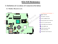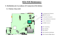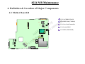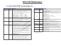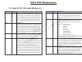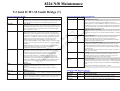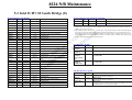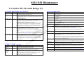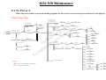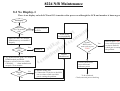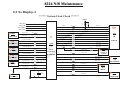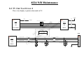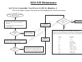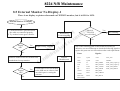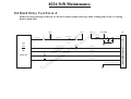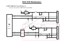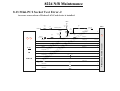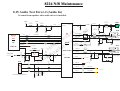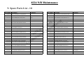
1
SERVICE MANUAL FOR 8224 BY: Star Meng Validation Tool Research Department /EDVD Mar.2006 / R01 8224 N/B Maintenance Contents 1. Hardware Engineering Specification ………………………………………………………………….. 4 1.1 Introduction …………………………………………………………………………………………………………… 4 1.2 Hardware System …………………………………………………………………………………………………….. 8 1.3 Other Functions ………………………………………………………………………………………………………. 38 1.4 Power Management ………………………………………………………………………………………………….. 44 1.5 Appendix 1: Intel ICH7-M GPIO Definitions ……………………………………………………………………… 47 1.6 Appendix 2: W83L951DG GPIO Definitions …………………….………………………………………………… 49 t t n e e r c m e 2. System View and Disassembly …………………………………………………………………………. u S c c o a D T l i ia M t n ……………………………………………………… 3. Definition & Location of Connectors / Switches e id f n o CMajor Components ………………………………………………………… 4. Definition & Location of 54 2.1 System View …………………………………………………………………………………………………………... 54 2.2 Tools Introduction ……………………………………………………………………………………………………. 57 2.3 System Disassembly ………………………………………………………………………………………………….. 58 78 3.1 Mother Board ………………………………………………………………………………………………………… 78 3.2 Daughter Board ………………………………………………………………………………………………………. 81 82 4.1 Mother Board ………………………………………………………………………………………………………… 82 5. Pin Description of Major Components …….………………………………………………………….. 84 5.1 Intel 945/945P North Bridge ………………………………………………………………………………………… 84 5.2 Intel ICH7-M South Bridge …………………………………………………………………………………………. 90 1 8224 N/B Maintenance Contents 6. System Block Diagram …………………………………………………………………………………. 101 7. Maintenance Diagnostics ………………………………………………………………………………. 102 7.1 Introduction ………………………………………………………………………………………………………….. 102 t t n e e r 8. Trouble Shooting ……………………………………………………………………………………….. c m e u S c c Do a iT ial M t n e id f n o C 7.2 Error Codes …………………………………………………………………………………………………………… 103 7.3 Debug Tool ……………………………………………………………………………………………………………. 105 107 8.1 No Power ……………………………………………………………………………………………………………… 109 8.2 No Display …………………………………………………………………………………………………………….. 115 8.3 TV Out Test Error …………………………………………………………………………………………………… 118 8.4 VGA Controller Test Error LCD No Display ………………………………………………………………………. 120 8.5 External Monitor No Display ………………………………………………………………………………………… 122 8.6 Memory Test Error …………………………………………………………………………………………………... 125 8.7 Keyboard (K/B) Touch-Pad (T/P) Test Error ……………………………………………………………………… 127 8.8 Hard Driver Test Error ……………………………………………………………………………………………… 129 8.9 CD-ROM Driver Test Error ………………………………………………………………………………………… 131 8.10 USB Port Test Error ………………………………………………………………………………………………… 133 8.11 New Card Socket Test Error ……………………………………………………………………………………….. 136 8.12 Blue Tooth Test Error ………………………………………………………………………………………………. 138 8.13 Mini-PCI Socket Test Error ………………………………………………………………………………………... 140 8.14 CardReader & IEEE1394 Socket Test Error ……………………………………………………………………… 143 8.15 Audio Test Error ……………………………………………………………………………………………………. 146 2 8224 N/B Maintenance Contents 8.16 LAN Test Error ……………………………………………………………………………………………………… 149 9. Spare Parts List ………………………………………………………………………………………… 151 10. System Exploded Views ……………………………………………………………………………….. 163 11. Reference Material ……………………………………………………………………………………. 165 t t n e e r c m e u S c c Do a iT ial M t n e id f n o C 3 8224 N/B Maintenance 1. Hardware Engineering Specification 1.1 Introduction 1.1.1 General Description t t n e e r c m e 1.1.2 System Overview u S c c Do a iT ial M t n e id f n o C This document describes the brief introduction for MiTAC 8224 portable notebook computer system. The MiTAC 8224 model is designed for Intel Mobile Pentium-M Processor Yonah 533 and 667 FSB. This system is based on PCI architecture and is fully compatible with IBM PC/AT specification, which has standard hardware peripheral interface. The power management complies with Advanced Configuration and Power Interface. It also provides easy configuration through CMOS setup, which is built in system BIOS software and can be pop-up by pressing F2 key at system start up or warm reset. System also provides icon LEDs to display system status, such as AC Power indicator, Battery Power indicator, Battery status indicator, HDD,CD-ROM, NUM LOCK, CAP LOCK, SCROLL LOCK. It also equipped with GIGA LAN, 56K Fax MODEM, 4 USB port, S-Video and audio line out, SPIDIF, and internal/external microphone function. The memory subsystem supports DDR2 SDRAM channels (64-bits wide). The 945GM MCH Host Memory Controller integrates a high performance host interface for Intel Yonah processor, 4 8224 N/B Maintenance a high performance PCI Express interface, a high performance memory controller, Digital Video port (DVOB & DVOC) interface, and Direct Media Interface (DMI) connecting with Intel ICH7-M. The Intel ICH7-M integrates three Universal Serial Bus 2.0 Host Controllers Interface (UHCI), the Audio Controller with Azalia interface, the Ethernet includes a 32-bit PCI controller, the IDE Master/Slave controllers, the SATA controller and Direct Media Interface technology. t t n e e r c m e u S c c Do a iT ial M t n e id f n o C Intel Graphics enhancements includes DVMT 3.0 , Zone Rendering 2.0, Quad pixel pipe rendering engine, Pixel Shader 2.0 and 4x Faster Setup Engine. The BCM5789 is a highly integrated, cost-effective single-chip Fast Ethernet controller that provides 32-bit performance, PCI bus master capability, and full compliance with IEEE 802.3u 100Base-T specifications and IEEE 802.3x Full Duplex Flow Control. It also supports the Advanced Configuration Power management Interface (ACPI). The Texas Instruments PCI8402 controller is an integrated single-socket IEEE 1394 open HCI host controller.and one-port PHY and flash media controller. This high-performance integrated solution provides the latest in IEEE 1394, SD, MMC, Memory Stick/PRO, SmartMedia, and xD technology. The ALC880 2-Channel High Definition Audio Codec with UAA (Universal Audio Architecture), featuring a 24-bit two-channel DAC and two stereo 20-bit ADCs, are designed for commercial Notebook PC system. The ALC880 provide 2 output channels, along with flexible mixing, mute, and fine gain control functions. Also, supporting 32-bit S/PDIF input and output functions and a sampling rate of up to 96kHz. The W83L951D is a high performance microcontroller on-chip supporting functions optimized for embedded control. These include ROM, RAM, four types of timers, a serial communication interface, optional I²C bus 5 8224 N/B Maintenance interface, host interface, A/D converter, D/A converter, I/O ports, and other functions needed in control system configurations, so that compact, high performance systems can be implemented easily. A full set of software drivers and utilities are available to allow advanced operating systems such as Windows ME, Windows 2000 and Windows XP to take full advantage of the hardware capabilities. Features such as bus mastering IDE, Plug and Play, Advanced Power Management (APM) with application restart, software-controlled power shutdown. t t n e e r c m e u S c c Do a iT ial M t n e id f n o C Following chapters will have more detail description for each individual sub-systems and functions. 6 8224 N/B Maintenance 1.1.3 System Parts Item Description CPU Mobile Pentium-M Processor Yonah 533 and 667 FSB Thermal spec 40 W TDP Core Logic System BIOS Memory HDD ODD Display Clock Generator Video Control LAN Card Reader + IEEE1394 Audio System Modem Wireless LAN CIR USB TV Tuner Card New Card Intel 945GM(PM) + ICH7-M chipset SST49LF004A DDR2 533 256 MB: Nanya NT256T64UH4A0FN-37B Micron MT4HTF3264HY-53EB3 DDR2 533 512 MB: Nanya NT512T64UH8A0FN-37B Micron MT8HTF6464HDY-53EB3 t t n e e r c m e u S c c Do a iT ial M t n e id f n o C SATA: Fujitsu: MHT2060BH, 60 GB PATA: Fujitsu: MHT2060AT+, 60 GB COMBO : Lite-On LSC-2483K or KME-UJDA760 14.1W”: AUO B141XG05 CHI-MEI N141I1-L02 ICS 9LPR310 Intel 945GM ATI: M56-P with 8 cells 32 MB GDDR2 memory BCM5787 PCI8402ZHK Azalia CODEC: ALC880 56 Kbps(V.90) Fax Modem(MDC(Azalia I/F)) and 10/100(Reserved for 1000) Base-TX LAN Ekron (10/100) or Vidalia (GbE) Wireless LAN Intel Pro/Wireless 3945ABG(Mini PCI-E Interface IEEE802.11a, b, g)with RF(USB interface) IRM-2638 USB2.0 x 4 (individual) Internal USB: Blue Tooth Mini-PCI-E AVerMedia Hybrid TV Tuner Card Mini-PCI-E interface 7 8224 N/B Maintenance 1.2 Hardware System 1.2.1 Intel Yonah Processors in Micro-FCBGA Package Intel Yonah Processors with 478 pins Micro-FCBGA package. The Yonah processor is built on Intel’s next generation 65 nanometer process technology. Yonah is Intel’s first dual core processor for mobile. The following list provides some of the key features on this processor: t t n e e r c m e u S c c Do a iT ial M t n e id f n o C • First dual core processor for mobile • Supports Intel Architecture with Dynamic Execution • On-die, primary 32 kB instruction cache and 32 kB write-back data cache • On-die, 2 MB second level cache with Advanced Transfer Cache Architecture • Data Prefetch Logic • Streaming SIMD Extensions 2 (SSE2) and Streaming SIMD Extensions 3 (SSE3) • The Yonah Standard Voltage and Low Voltage processor are offered at 667 MHz FSB • The Yonah Ultra Low Voltage processor is offered at 533 MHz FSB • Advanced Power Management features including Enhanced Intel SpeedStep technology • Digital Thermal Sensor • Micro-FCPGA and Micro-FCBGA packaging technologies 8 8224 N/B Maintenance • Execute Disable Bit support for enhanced security • Intel Virtualization Technology 1.2.2 Clock Generator t t n e e r c m e u S c c Do a iT ial M t n e id f n o C ICS9LPR310 is a low power CK410M-compliant clock specification. This clock synthesizer provides a single chip solution for next generation P4 Intel processors and Intel chipsets. ICS9LPR310 is driven with a 14.318MHz crystal. Output Features: • 2 - 0.7 V differential CPU pairs • 8 - 0.7 V differential PCIEX pairs • 1 - 0.7 V differential SATA pair • 1 - 0.7 V differential LCDCLK/PCIEX selectable pair • 4 - PCI (33 MHz) • 2 - PCICLK_F, (33 MHz) free-running • 1 - USB, 48 MHz • 1 - DOT 96 MHz/27 MHz selectable pair • 2 - REF, 14.318 MHz 9 8224 N/B Maintenance Key Specifications: • CPU outputs cycle-cycle jitter < 85ps • PCIEX outputs cycle-cycle jitter < 125ps • SATA outputs cycle-cycle jitter < 125ps • PCI outputs cycle-cycle jitter < 500ps t t n e e r c m e u S c c Do a iT ial M t n e id f n o C • +/- 300ppm frequency accuracy on CPU, PCIEX and SATA clocks • +/- 100ppm frequency accuracy on USB clocks Features/Benefits: • Supports tight ppm accuracy clocks for Serial-ATA and PCIEX • Supports programmable spread percentage and frequency • Uses external 14.318 MHz crystal, external crystal load caps are required for frequency tuning 10 8224 N/B Maintenance 1.2.3 The Mobile Intel 945GM Express Chipset The Mobile Intel 945GM Express Chipset is designed for use in Intel’s next generation mobile platform,code named NAPA. The Intel 945GM Express Chipset come with the Generation 3.5 Intel Integrated Graphics Engine,and the Intel Graphics Media Accelerator (GMA) 950,providing enhanced graphics support over the previous generation(G)MCH’s. t t n e e r c m e u S c c Do a iT ial M t n e id f n o C The (G)MCH manages the flow of information between the four following primary interfaces: • FSB • System Memory Interface • Graphics Interface • DMI The (G)MCH can also be enabled to support external graphics,using the x16 PCI Express Graphics attch port.When external graphics is enabled,the internal graphics port are inactive. Features Processor Support • All Yonah variants 11 8224 N/B Maintenance • Merom support • 533 MHz and 667MHz Front Side Bus (FSB) support • Source synchronous double-pumped (2x) Address • Source synchronous quad-pumped (4x) Data • Other key features are: t t n e e r c m e u S c c Do a iT ial M t n e id f n o C -- Support for DBI (Data Bus Inversion) -- Support for MSI (Message Signaled Interrupt) -- 32-bit interface to address up to 4 GB of memory -- A 12 deep In-Order Queue to pipeline FSB commands -- GTL+ bus driver with integrated GTL termination resistors Memory System • Support Single/Dual Channel DDR2 SDRAM • Maximum Memory supported 2 GB • 64 bit wide per channel • Three Memory Channel Configurations supported -- Single Channel -- Dual Channel Symmetric 12 8224 N/B Maintenance -- Dual Channel Asymmetric • One SO-DIMM connector per channel • Support for DDR2 at 400MHz, 533MHz and 667MHz • 256Mb , 512Mb and 1 Gb Memory Technologies supported • Support for x8 and x16 devices t t n e e r c m e u S c c Do a iT ial M t n e id f n o C • Maximum Memory supported: 2 GB • Support for DDR2 On-Die Termination (ODT) • Supports Partial Writes to memory using Data Mask signals (DM) • Intel Rapid Memory Power Management • Dynamic row power-down • No support for Fast Chip Select mode • Support for 2N timings only Discrete Graphics using PCI Express • One 16-lane (x16) PCI Express port for external PCI Express Based graphics card • Fully compliant to the PCI Express Base Specification revision 1.0a. base PCI Express frequency of 2.5 GHz only 13 8224 N/B Maintenance • Raw bit-rate on the data pins of 2.5Gb/s, resulting in a real bandwidth per pair of 250 MB/s given the 8/10 encoding used to transmit data across this interface • Maximum theoretical realized bandwidth on interface of 4 GB/s in each direction simultaneously, for an aggregate of 8 GB/s when x16 • 100 MHz differential reference clock (shared by PCI Express Gfx and DMI) • STP-AGP/AGP_BUSY Protocol equivalent for PCI Express based attach is via credit based PCI Express mecanism t t n e e r c m e u S c c Do a iT ial M t n e id f n o C • PCI Express power management support: L0s, L1, L2/L3 Ready, L3 • Lane# 0 only for signaling and detection of exit from L0s and L1 • Hierarchical PCI-compliant configuration mechanism for downstream devices (i.e., normal PCI 2.2 Configuration space as a PCI-to-PCI Bridge) • PCI Express Extended Configuration Space. The first 256 bytes of configuration space aliases directly to the PCI Compatibility configuration space. The remaining portion of the fixed 4KB block of memory-mapped space above that (starting at 100h) is known as extended configuration space • PCI Express Enhanced Addressing Mechanism. Accessing the device configuration space in a flat memory mapped fashion • Automatic discovery, negotiation, and training of link out of reset • Supports traditional PCI style traffic (asynchronous snooped, PCI ordering) • Supports traditional AGP style traffic (asynchronous non-snooped, PCI-X Relaxed ordering) • Support for peer segment destination write traffic (no peer-to-peer read traffic) in Virtual Channel 0 only 14 8224 N/B Maintenance • APIC and MSI interrupt messaging support. Will send Intel-defined “End Of Interrupt” broadcast message when initiated by the CPU • Support for Isochronous non-snooped traffic through a dedicated Virtual Channel • Downstream Lock Cycles(including Split Locks) • Automatic clock extraction and phase correction at the receiver Internal Graphics t t n e e r c m e u S c c Do a iT ial M t n e id f n o C • Intel Gen 3.5 Integrated Graphics Engine • 250 MHz core rendor clock at 1.05V core voltage • Supports TV-Out, LVDS, CRT and SDVO • Intel Dual Frequency Graphics Technology • Intel Dynamic Video Memory Technology (DVMT 3.0) • Intel Smart 2D Display Technology • Intel Display Power Saving Technology 2.0 • Video Capture via x1 concurrent PCIE port • Higher Performance MPEG-2 Decoding • Hardware Acceleration for VLD / iDCT • 4x pixel rate HWMC 15 8224 N/B Maintenance • DX 9.1 • Hardware Motion Compensation • Intermediate Z in Classic Rendering Analog CRT t t n e e r c m e u S c c Do a iT ial M t n e id f n o C • Integrated 400 MHz RAMDAC • Analog Monitor Support up to QXGA (2048 x 1536) • Support for CRT Hot Plug Dual Channel LVD • Panel support up to UXGA (1600 x 1200) • 25-112 MHz single / dual channel -- Single channel LVDS interface support: 1 x 18 bpp -- Dual channels LVDS interface support: 2 x 18 bpp panel support up to UXGA (1600 x 1200) -- TFT panel type supported • Pixel Dithering for 18 bit TFT panel to emulate 24 bpp true color displays • Panel Fitting. Panning , and Center Mode Supported • CPIS 1.5 compliant 16 8224 N/B Maintenance • Spread spertrum clocking supported • Panel Power Sequencing support • Integrated PWM interface for LCD backlight inberter control TV - OUT t t n e e r c m e u S c c Do a iT ial M t n e id f n o C • Three integrated 10 bit DACS • Macro Vision support • Overscaling • NTSC / PAL • Component, S-Video and Composite Output interfaces • HDTV support -- Single channel LVDS interface support: 1 x 18 bpp DMI • Chip-to-chip interface between (G)MCH and Intel 82801GBM (ICH7M) • Configurable as x2 or x4 DMI lanes • 2 GB/s (1 GB/s each direction) point-to-point interface to Intel 82801GBM 17 8224 N/B Maintenance • 32 bit downstream address • Direct Media Interface asynchronously coupled to core • Supports 3 Virtual Channels for traffic class performance differentiation • Supports both snooped and non-snooped traffic • Supports isochronous non-snooped traffic t t n e e r c m e u S c c Do a iT ial M t n e id f n o C • Supports legacy snooped isochronous traffic • Supports the following traffic types to or from Intel 82801GBM • Peer write traffic between DMI and PCI Express Graphics port • DMI-to-DRAM • DMI-to-CPU (FSB Interrupts or MSIs only) • CPU-to-DMI • Messaging in both directions, including Intel Vendor-specific messages • Supports Power Management state change messages • APIC and MSI interrupt messaging support • Supports SMI, SCI and SERR error indication • Legacy support for ISA regime protocol (PHOLD/PHOLDA) required for parallel port DMA, floppy drive, and LPC bus masters 18 8224 N/B Maintenance 1.2.4 I/O Controller Hub : INTEL ICH7-M The ICH7 provides extensive I/O support. Functions and capabilities include: • PCI Express Base Specification, Revision 1.0a support • PCI Local Bus Specification, Revision 2.3 support for 33 MHz PCI operations ( supports up to six Req/Gnt pairs) t t n e e r c m e u S c c Do a iT ial M t n e id f n o C • ACPI Power Management Logic Support • Enhanced DMA controller, interrupt controller, and timer functions • Integrated Serial ATA host controller with independent DMA operation on four ports and AHCI (ICH7R only)support • USB host interface with support for eight USB ports; four UHCI host controllers; one EHCI high-speed USB 2.0 Host controller • Integrated LAN controller • System Management Bus (SMbus) Specification, Version 2.0 with additional support for I2C devices • Supports Audio Codec ’97, Revision 2.3 Specification (a.k.a , AC ’97 Component Specification, Revision 2.3) which provides a link for Audio and Telephony codecs (up to 7 channels) • Supports Intel High Definition Audio • Supports Intel Matrix Storage Technology (ICH7R only) • Supports Intel Active Management Technology 19 8224 N/B Maintenance • Low Pin Count (LPC) interface • Firmware Hub (FWH) interface support • Serial Peripheral Interface (SPI) support t t n e e r c m e u S c c Do a iT ial M t n e id f n o C 1.2.5 VGA Controller: ATI M56-P The M52-P is based on PCI Express technology and leverages a brand new graphics architecture. Based on 90nm micron process technology, the M52-P will deliver a 16-lane PCI Express bus interface and lead-free ASIC. Features Processor / Host Bus Support • Support for Microsoft® DirectX® 9.0 programmable vertex and pixel shaders in hardware. • Shader model 3.0 vertex and pixel shader support: • Full speed 32-bit floating point processing • High dynamic range rendering with floating point blending support • High performance dynamic branching and flow control • Complete feature set also supported in OpenGL® 2.0. 20 8224 N/B Maintenance Anti-Aliasing and Anisotropic Filtering • 2x/4x/6x Anti-Aliasing modes • Sparse multi-sample algorithm with gamma correction, programmable sample patterns, and centroid sampling • Lossless Color Compression (up to 6:1) at all resolutions, including widescreen HDTV resolutions • Temporal Anti-Aliasing t t n e e r c m e u S c c Do a iT ial M t n e id f n o C • 2x/4x/8x/16x Anisotropic Filtering modes • Up to 128-tap texture filtering • Adaptive algorithm with performance and quality options 3Dc+™ — Advanced Texture Compression • High quality 4:1 compression for normal maps and luminance maps • Works with any single-channel or two-channel data format Next-Generation HYPER Z™ Technology • Hierarchical Z-Buffer with Early Z Test • Lossless Z-Buffer Compression (up to 48:1) • Fast Z-Buffer Clear 21 8224 N/B Maintenance • Z Cache optimized for real-time shadow rendering • Optimized for performance at high display resolutions, including widescreen HDTV resolutions High Performance Memory Support • Support for DDR1 and DDR2 SDRAM/SGRAM, and GDDR3 SDRAM (except M56-P) t t n e e r c m e u S c c Do a iT ial M t n e id f n o C Programmable Video Processing Engine • Seamless integration of pixel shaders with video in real time • FULLSTREAM™ video de-blocking technology for Real, DivX, and WMV9 formats • VIDEOSOAP™ noise removal filtering for captured video • MPEG1/2/4 decode and encode acceleration • DXVA Support • Hardware Motion Compensation, iDCT, DCT and color space conversion • All-format DTV/HDTV decoding • YPrPb component output for direct drive of HDTV displays • Adaptive Per-Pixel De-Interlacing and Frame Rate Conversion (temporal filtering) • Dual integrated display controllers 22 8224 N/B Maintenance • Dual integrated 10 bit per channel 400 MHz DACs • Integrated 165 MHz TMDS transmitter (DVI 1.0 / HDMI compliant and HDCP ready) • Additional external TMDS support for dual-link DVI • Integrated TV Output support up to 1024x768 resolution t t n e e r c m e u S c c Do a iT ial M t n e id f n o C 1.2.6 AZALIA AUDIO SYSTEM: ALC880 ALC880 provides 7.1 channels of outputs and multiple stereo inputs, along with flexible mixing, mute and finer gain control functions to provide a complete integrated audio solution for PCs. Also the highest 192KHz sample rate DACs and Realtek proprietary hardware content protection are applicable for DVD Audio, which only implemented in high end consumer electronics, now is achieved by PCs with ALC880 inside. ALC880 is also the one and only High Definition Audio Codec integrating three pairs of stereo ADCs which can support microphone array with AEC (Acoustic Echo Cancellation), BF (Beam Forming) and NS (Noise Suppression) technology simultaneously to significantly improve recording quality for conference call. With this unique feature (3 pairs of Stereo ADCs), ALC880 can perform the ultimate performance of HAD like using S/PDIF to output analog data or multiple recording application. Features • High performance DACs with 95dB S/N ratio • Meets performance requirements for audio on PC2001 systems 23 8224 N/B Maintenance • 8 channels of DAC support 16/20/24-bit PCM format for 7.1 audio solution • 3 stereo ADCs support 16/20-bit PCM format, two for microphone array, one for legacy mixer recording • Supports 44.1K/48K/96K/192KHz DAC sample rate • All ADCs support 44.1K/48K/96K sample rate • Applicable for 4ch/192KHz and 6ch/96KHz DVD-Audio solution t t n e e r c m e u S c c Do a iT ial M t n e id f n o C • Up to 4 channels of microphone input are supported for AEC/BF application • Support Power Off CD function • Support external PCBEEP input and built in BEEP generator • PCBEEP Pass-Through when link is in RESET state • Software selectable 2.5V/3.75V VREFOUT • Default 6 VREFOUTs are supported, additional 4 VREFOUTs are capable by sharing un-used analog I/O pins • 2 jack detection pins each supports up to 4 jacks plugging can be detected • 16/20/24-bit S/PDIF-OUT supports 44.1K/48K/96KHz sample rate • 16/20/24-bit S/PDIF-IN supports 44.1K/48K/96KHz sample rate • Optional EPAD (External Amplifier Power Down) is supported • Power support: Digital: 3.3V; Analog: 3.3V/5.0V • Power management and enhanced power saving features 24 8224 N/B Maintenance • 48-pin LQFP package is compatible with AC’97 • Reserve analog mixer architecture is backward compatible with AC’97 • –64dB ~ +30dB with 1dB resolution of mixer gain to achieve finer volume control • Impedance sensing capability for each re-tasking jack • All analog jacks are stereo input and output re-tasking for analog plug & play t t n e e • r c m e • u S c c o • a D T l i ia M t nCard (MDC56AZS2) 1.2.7 MDC: Azalia MDC Modem e id f n o C • Built in headphone amplifier for each re-tasking jack Support external volume knob control Support 2 GPIO (General Purpose Input/Output) for customized application Hardware content protection for DVD-Audio supporting Features • AC’97/MC’97 2.2 compliant • MDC Modem support current sense, whenever the current on the line exceeds approximately 150mA, and should immediately go back on hook • ITU-T V.92 PCM Upstream and V.90 data rates with auto0fallback to V.34, V.32ter V.32 bis and fallbacks 25 8224 N/B Maintenance • Virtual Com port with a through put of up to 460.8Kbps • V.42 bis/MNP 5 data compression • FAX: Send and receive rates up to 14.4kbps, V.17, V.29, V.27ter • Hayes AT Command set • Supports V.42 error correction and V.44, V.42bis/MNP5 data compression t t n e e • r c m e u S c c o a 1.2.8 System Flash Memory (BIOS) D iT ial M t • n e • id f n o C • FAX capabilities: ITU-T V.17, V.29, V.27ter, V.21 Ch2 and TIA/EIA 578 Class1 FAX Modem Support Wake up on Ring Firmware Hub for Intel® 810, 810E, 815, 815E,815EP, 820, 840, 850 Chipsets Flexible Erase Capability -- Uniform 4 KByte Sectors -- Uniform 16 KByte overlay blocks for SST49LF002A -- Uniform 64 KByte overlay blocks for SST49LF004A -- Top boot block protection -- 16 KByte for SST49LF002A -- 64 KByte for SST49LF004A 26 8224 N/B Maintenance -- Chip-Erase for PP Mode • Single 3.0-3.6V Read and Write Operations • Superior Reliability • Firmware Hub Hardware Interface Mode -- 5-signal communication interface supporting byte Read and Write t t n e e r c m e u S c c Do a iT ial M t n e id f 1.2.9 Memory Systemon C -- 33 MHz clock frequency operation -- WP# and TBL# pins provide hardware write protect for entire chip and/or top Boot Block -- Block Locking Register for all blocks -- Standard SDP Command Set -- Data# Polling and Toggle Bit for End-of-Write detection -- 5 GPI pins for system design flexibility -- 4 ID pins for multi-chip selection 128MB, 256MB, 512MB, 1GB (x64) 200-Pin DDR2 SDRAM SODIMMs • JEDEC-standard 200-pin, small-outline, dual in-line memory module (SODIMM) • VDD=+1.8V±0.1V, VDDQ=+1.8V±0.1V 27 8224 N/B Maintenance • JEDEC standard 1.8V I/O (SSTL_18-compatible) • Differential data strobe (DQS,DQS#) option • Four-bit prefetch architecture • Differential clock input (CK,CK#) • Command entered on each rising CK edge t t n e e r c m e u S c c Do a iT ial M t n e id f n o C • DQS edge-aligned with data for Reads • DQS center-aligned with data for Writes • Duplicate output strobe (RDQS) option for x8 configuration • DLL to align DQ and DQS transitions with CK • Four internal banks for concurrent operation • Data mask (DM) for masking write data • Programmable CAS Latency (CL): 2,3,4 and 5 • Posted CAS additive latency (AL): 0,1,2,3 and 4 • Write latency = Read latency – 1tCK • Programmable burst lengths: 4 or 8 • Read burst interrupt supported by another READ • Write burst interrupt supported by another WRITE 28 8224 N/B Maintenance • Adjustable data – output drive strength • Concurrent auto precharge option is supported • Auto Refresh (CBS) and Self Refresh Mode • 64ms, 8,192-cycle refresh • Off-chip drive (OCD) impedance calibration t t n e e r c m e u S 1.2.10 GIGALAN – BCM5787 c c Do a iT ial M t n e id f n o C • On-die termination (ODT) The BCM5787 is a seventh generation 10/100/1000BASE-T Ethernet LAN controller solution for highperformance network applications. The device combines a triple-speed IEEE 802.3 compliant Media Access Controller (MAC) with a triple-speed Ethernet transceiver, 1x PCI-E bus interface, and on-chip buffer memory in a single device. The device is fabricated in a 1.2V CMOS process providing a low-power system solution. Features • Integrated 10/100/1000BASE-T transceiver • Automatic MDI crossover function • PCI-E v1.0a • 10/100/1000BASE-T full/half-duplex MAC 29 8224 N/B Maintenance • Wake on LAN support meeting the ACPI requirements • Statistics for SNMP MIB II, Ethernet-like MIB, and Ethernet MIB (802.3z, clause 30) • Serial EEPROM or serial flash support • JTAG support • 196-FBGA package t t n e e r 1.2.11 Keyboard System: Winbond W83L951DG c m e u S c c Do a iT ial M t n e id f n o C The Winbond mobile keyboard and embedded controller W83L951D/F architecture consists of a Turbo-8051 core logic controller and surrounded by various components, 2K+256 bytes of RAM, 64K on-chip FLASH, LPC host interface, 13 general purpose I/O port with 24 external interrupt source, 4 timers, 1 serial port, 2 SMBus interface for master mode, 3 PS/2 port, two 8-bits and two 16-bits PWM channels, 2 D-A and 8 A-D converters, 1 Consumer Infrared Communications Receiver, 2 Fan Tachometer , 1 Real Time Clock Generator, and Matrix Interface. The part number with an affix of “G” is the Lead-free package product. Core logic • 8-bit Turbo 8052 Microprocessor Code based, Speed up to 24MHz • 256 bytes Internal RAM • 64K bytes Embedded Programmable Flash Memory 30 8224 N/B Maintenance • 2K bytes External SRAM Host interface • Software Optional with LPC Interface • Primary Programmable I/O Address Communication Port in LPC Mode t t n e e r c m e u S c c Do a iT ial M t n e id f n o C • Support SERIRQ in LPC Interface • Support Hardware Fast Gate A20 and KBRST • Support Port 92h SMBus • Support 2 SMBus Interface support Master Mode Timers • Support Four Timer Signal with Three Pre-scalars • Timer 1 and 2 Shard the Same Pre-scalar and are Free-Running Only • Timer X and Y Have Individual Pre-scalar and Support up to Four Control Modes, Free • Running, Pulse Output, Event Counter and Pulse Width Measurement 31 8224 N/B Maintenance PWM • Support Four PWM Channels • PWM 0 and 1 are 8-bits and Programmable Frequency from 62Hz to 7.5 KHz • PWM 2 and 3 are 16-bits and Programmable Frequency from 6Hz to 3MHz Fan Tachometer t t n e e r c m e u S c c Do a iT ial M t n e id f n o C • Support two Fan Tachometer Inputs A/D Converter • Firmware Programmable Optional with 10-bite or 8-bit Resolution • Support Eight Channels D/A Converter • 8-bit Resolution • Support Two Channels 32 8224 N/B Maintenance PS2 • Support Three Hardware PS2 Channels • Optional PS2 Clock Inhibit by Hardware or Firmware Keyboard Controller t t n e e r c m e u S c c Do a iT ial M t n e id f n o C • Support 16*8 Keyboard Matrix-scan, Expanding to 18*8 and 20*8 GPIO • Support 104 Useful GPIO Pins Totally and Bit–addressable to Facility Firmware Coding FLASH • Support External On-Board 64K Flash via Matrix Interface (GP0, 1, 3) CIR • Support Decoding for the NEC Consumer IR Remote Control Format 33 8224 N/B Maintenance RTC • Real Time Clock Generator with 32.768 KHz Input ACPI • Support ACPI Appliance t t n e e r c m e u S c c Do • a iT ial M t n 1.2.12 Hard Disk Drive e id f n o C • Secondary Programmable I/O Address Communication Port in LPC Mode Package 128 Pin QFP and 128 Pin LQFP Package Options 8224 can support SATA or PATA HDD by equipped different HDD transition board. SATA HDD The SATA function in the ICH7 has dual modes of operation to support different operating system conditions. In the case of Native IDE enabled operating systems, the ICH7 has separate PCI functions for serial and parallel ATA (“enhanced mode”). To support legacy operating systems, there is only one PCI function for both the serial and 34 8224 N/B Maintenance parallel ATA ports if functionality from both SATA and PATA devices is desired (“combined mode”). SATA interface transfer rates are independent of UDMA mode settings. SATA interface transfer rates will operate at the bus’s maximum speed, regardless of the UDMA mode reported by the SATA device or the system BIOS. -- Up-to 150MB/sec bus speed (Serial ATA Generation 1) -- Compliant with Serial ATA 1.0a Specification and Serial ATA 2 Extensions 1.0 -- Supports 48bit-LBA addressing t t n e e r c m e u S c c Do a iT ial M t n e id f n o C -- Supports Native DMA Queued command (First party DMA queued) -- Also supports Legacy DMA Queued command -- Supports Staggered Spin-Up function -- Supports Hot-Plug features -- Supports Serial ATA power management (Host initiated Partial/Slumber) IDE HDD The ICH7 IDE controller features one set of interface signals that can be enabled, tri-stated or driven low. The IDE interfaces of the ICH7 can support several types of data transfers: -- Programmed I/O (PIO): processor is in control of the data transfer -- 8237 style DMA: DMA protocol that resembles the DMA on the ISA bus, although it does not use the 8237 in the ICH7. This protocol off loads the processor from moving data. This allows higher transfer rate of up to 16MB/s -- Ultra ATA/33/66/100: DMA protocol that redefines signals on the IDE cable to allow both host and target throttling of data and transfer rates of up to 33/66/100 MB/s 35 8224 N/B Maintenance 1.2.13 CIR The TSOP62.. - series are miniaturized SMD-IR Receiver Modules for infrared remote control systems. PIN diode and preamplifier are assembled on lead frame, the epoxy package is designed as IR filter. The demodulated output signal can directly be decoded by a microprocessor. TSOP62.. is the standard IR remote control SMD-Receiver series, supporting all major transmission codes. Features t t n e e r c m e u S c c Do a iT ial M t n e id f n o C Photo detector and preamplifier in onepackage • Internal filter for PCM frequency • Continuous data transmission possible • TTL and CMOS compatibility • Output active low • Low power consumption • High immunity against ambient light • Low power consumption • Lead (Pb)-free component • Component in accordance to RoHS 2002/95/EC and WEEE 2002/96/EC 36 8224 N/B Maintenance 1.2.14 Card Reader & IEEE 1394 – PCI8402ZHK The PCI8402 controller is a four-function PCI controller compliant with PCI Local Bus Specification, It is 216 ball PBGA package. Function 0 is a dummy PC Card controller function. The PC Card socket is non-functional and the pins associated with the PC card socket may be left unconnected. The function is required for device enumeration and is provided for BIOS compatibility with existing devices. The PC Card function may be hidden from the OS by the BIOS. t t n e e r c m e u S c c Do a iT ial M t n e id f n o C Function 1 of the PCI8402 controller is compatible with IEEE Std 1394a-2000 and the latest 1394 Open Host Controller Interface Specification. The chip provides the IEEE1394 link and 1-port PHY function and is compatible with data rates of 100, 200, and 400 Mbits per second. Deep FIFOs are provided to buffer 1394 data and accommodate large host bus latencies. The PCI8402 controller provides physical write posting and a highly tuned physical data path for SBP-2 performance. Function 2 of the PCI8402 controller is a PCI-based Flash Media controller that supports Memory Stick, Memory Stick-Pro, SmartMedia, xD, SD, and MMC cards. This function controls communication with these Flash Media cards through a dedicated Flash Media socket. In addition, this function includes DMA capabilities for improved Flash Media performance. Function 3 of the PCI8402 controller is a PCI-based SD host controller that supports MMC, SD, and SDIO cards. This function controls communication with these Flash Media cards through a dedicated Flash Media socket. In addition, this function is compliant with the SD Host Controller Standard Specification and includes both DMA capabilities and support for SD suspend/resume. 37 8224 N/B Maintenance 1.3 Other Functions 1.3.1 Hot Key Function Keys Combination Fn + F1 Fn + F3 Fn + F4 Fn + F5 Fn + F6 Fn + F7 Fn + F8 Fn + F10 Fn + F11 Fn + F12 Feature Power down Meaning Mini PCI power down t t n e e r c m e u S c c Do a iT ial M t n e id f n o C Reserve Volume down Volume up LCD/external CRT switching Rotate display mode in LCD only, CRT only, and simultaneously display Brightness down Decreases the LCD brightness Brightness up Increases the LCD brightness Mute Audio Mute Panel Off/On T oggle Panel on/off Suspend to DRAM / HDD Force the computer into either Suspend to HDD or Suspend to DRAM mode depending on BIOS Setup 1.3.2 Power On/Off/Suspend/Resume Button 1.3.2.1 APM Mode At APM mode, power button is on/off system power. 38 8224 N/B Maintenance 1.3.2.2 ACPI Mode At ACPI mode, Windows power management control panel set power button behavior. You could set “standby” , “power off” or “hibernate” (must enable hibernate function in power management) to power button function. Continue pushing power button over 4 seconds will force system off at ACPI mode. t t n e e r 1.3.3 Cover Switch c m e u S c c Do a iT ial M t n e id f n o C System automatically provides power saving by monitoring Cover Switch. It will save battery power and prolong the usage time when user closes the notebook cover. At ACPI mode there are four functions to be chosen at windows power management control panel. 1. None 2. Standby 3. Off 4. Hibernate (must enable hibernate function in power management) 39 8224 N/B Maintenance 1.3.4 LED Indicators 1.3.4.1 Five LED Indicators at Front Side: From left to right that indicates POWER, Battery Status, HDD/CD-ROM, NUM LOCK, CAP LOCK, SCROLL LOCK, WLAN. -- POWER: t t n e e r c m e u S c c Do a iT ial M t n e id f n o C This LED lights bule when the notebook was powered by AC or battery power line, Flashes orange (on 1 second, off 1 second) when entered suspend to RAM state . The LED is off when the notebook is in power off state. -- BATTERY STATUS: With battery operation, this LED stays off. When the battery charge drops to 10% of capacity, the LED lights red, flashes per 1 second and beeps per 2 second. When AC is connected, this indicator glows blue if the battery pack is fully charged or orange (amber) if the battery is being charged. System has five status LED indicators at front side which to display system activity. HDD/CD-ROM, NUM LOCK, CAPS LOCK, SCROLL LOCK and WLAN. 40 8224 N/B Maintenance 1.3.5 Battery Status 1.3.5.1 Battery Warning System also provides Battery capacity monitoring and gives users a warning signal to alarm they to store data before battery dead. This function also protects system from mal-function while battery capacity is low. t t n e e r c m e u S c 1.3.5.2 Battery Low State c Do a iT ial M t n e 1.3.5.3 Battery Dead State fid n o C Battery Warning: Capacity below 10%, Battery Capacity LED flashes per second, system beeps per 2 seconds. System will Suspend to HDD after 2 Minutes to protect users data. After Battery Warning State, and battery capacity is below 5%, system will generate beep sound for twice per second. When the battery voltage level reaches 8.56 volts, system will shut down automatically in order to extend the battery packs' life. 41 8224 N/B Maintenance 1.3.6 Fan Power on/off Management FAN is controlled by W83L951DG embedded controller-using ADM1032 to sense CPU temperature and PWM control fan speed. Fan speed is depended on CPU temperature. Higher CPU temperature faster Fan Speed. t t n e e r c m e u S c c Do a iT ial M t n e id f n o C 1.3.7 CMOS Battery CR2032 3V 220mAh lithium battery When AC in or system main battery inside, CMOS battery will consume no power. AC or main battery not exists, CMOS battery life at less (220mAh/5.8uA) 4 years. 1.3.8 I/O Port One Power Supply Jack One External CRT Connector For CRT Display Supports four USB port for all USB devices One MODEM RJ-11 phone jack for PSTN line One RJ-45 for LAN 42 8224 N/B Maintenance One IEEE1394 port One S/PDIF Jack. One Microphone Input Jack. One S-Video (PAL/NTSC) connector One Express Card Jack t t n e e r c m e u S 1.3.9 Battery Current Limit and Learning c c Do a iT ial M t n e id f n o C Two MINI PCI-E Jack for WLAN & TV Tuner Card Implanted H/W current limit and battery learning circuit to enhance protection of battery. 43 8224 N/B Maintenance 1.4 Power Management The 8224 system has built in several power saving modes to prolong the battery usage for mobile purpose. User can enable and configure different degrees of power management modes via ROM CMOS setup (booting by pressing F2 key). Following are the descriptions of the power management modes supported. t t n e e r c m e u S c c Do a iT ial M t n e id f n o C 1.4.1 System Management Mode Photo detector and preamplifier in onepackage • In this mode, each device is running with the maximal speed. CPU clock is up to its maximum. Doze Mode • In this mode, CPU will be toggling between on & stop grant mode either. The technology is clock throttling. • This can save battery power without loosing much computing capability. • The CPU power consumption and temperature is lower in this mode. Standby Mode • For more power saving, it turns of the peripheral components. In this mode, the following is the status of each device: 44 8224 N/B Maintenance -- CPU: Stop grant -- LCD: backlight off -- HDD: spin down Suspend to DRAM t t n e e r c m e u S c c Do a iT ial M t n e id f n o C • The most chipset of the system is entering power down mode for more power saving. In this mode, the following is the status of each device: 1. Suspend to DRAM -- CPU: off -- Intel 915GM: Partial off -- VGA: Suspend -- PCMCIA: Suspend -- Audio: off -- SDRAM: self refresh 2. Suspend to HDD -- All devices are stopped clock and power-down -- System status is saved in HDD -- All system status will be restored when powered on again 45 8224 N/B Maintenance 1.4.2 Other Power Management Functions HDD & Video access System has the ability to monitor video and hard disk activity. User can enable monitoring function for video and/or hard disk individually. When there is no video and/or hard disk activity, system will enter next PMU state depending on the application. When the VGA activity monitoring is enabled, the performance of the system will have some impact. t t n e e r c m e u S c c Do a iT ial M t n e id f n o C 46 8224 N/B Maintenance 1.5 Appendix 1: Intel ICH7-M GPIO Definitions (1) Pin Name GPIO0 GPIO1 GPIO2 GPIO3 GPIO4 GPIO5 GPIO6 GPIO7 GPIO8 GPIO9 GPIO10 GPIO11 GPIO12 GPIO13 GPIO14 GPIO15 GPIO16 GPIO17 GPIO18 GPIO19 GPIO20 GPIO21 GPIO22 GPIO23 GPIO24 GPIO25 GPIO26 Current Define PM_BMBUSY# MINIPCI_ACT# PCI_INTE# PCI_INTF# PCI_INTG# PCI_INTH# W_DISABLE# SCI# EXTSMI# X X SMBALERT# X X X TV_DISABLE# DPRSLPVR X STOP_PCI# PANEL_ID1 STOP_CPU# PANEL_ID0 PCI_REQ4# CRT_IN# X SPK_OFF SB_BT_ON# Input/Output I/O I/O I/O I/O I/O I/O I/O I/O I/O I/O I/O I/O I/O I/O I/O I/O I/O I/O I/O I/O I/O I/O I/O I/O I/O I/O I/O Function BM BUSY MINIPCI in detect PCI interrupt for LAN PCI interrupt for MINIPCI PCI interrupt for IEEE 1394 pull high for PCI Wireless LAN disable Sytem Control Interrupt SMI signal for chipset X X SMBus alert X X X TV disable Deeper Sleep X PCI stop Panel ID CPU stop Panel ID PCI Request CRT detect X Speak off Blue Tooth in detect Power Well t t n e e r c m e u S c c Do a iT ial M t n e id f n o C CORE CORE CORE CORE CORE CORE CORE CORE RESUME RESUME RESUME RESUME RESUME RESUME RESUME RESUME CORE CORE CORE CORE CORE CORE CORE CORE RESUME RESUME RESUME 47 8224 N/B Maintenance 1.5 Appendix 1: Intel ICH7-M GPIO Definitions (2) Continue to the previous page Pin Name GPIO27 GPIO28 GPIO29 GPIO30 GPIO31 GPIO32 GPIO33 GPIO34 GPIO35 GPIO36 GPIO37 GPIO38 GPIO39 GPIO48 GPIO49 Current Define Input/Output Function X X X X X PCLKRUN# WIRELESS_PD# LAN_ENABLE# X PANEL_ID2 X MB_ID0 MB_ID1 I/O I/O I/O I/O I/O I/O I/O I/O I/O I/O I/O I/O I/O X X X X X Clock run Wireless power down LAN enable X Panel ID X Mother Board ID Mother Board ID X I/O X HPWRGD I/O CPU power good Power Well t t n e e r c m e u S c c Do a iT ial M t n e id f n o C RESUME RESUME RESUME RESUME RESUME CORE CORE CORE CORE CORE CORE CORE CORE CORE V_CPU_IO 48 8224 N/B Maintenance 1.6 Appendix 2: W83L951DG GPIO Pins Definitions (1) Pin Name Pin No. 915 Pin Definitions I/O Hi/Low Function Port 0 GP00 94 KB OUT 0 O Key matrix scan output 0 GP01 93 KB OUT 1 O Key matrix scan output 1 GP02 92 KB OUT 2 O Key matrix scan output 2 GP03 91 KB OUT 3 O Key matrix scan output 3 GP04 90 KB OUT 4 O Key matrix scan output 4 GP05 89 KB OUT 5 O Key matrix scan output 5 GP06 88 KB OUT 6 O Key matrix scan output 6 GP07 87 KB OUT 7 O Key matrix scan output 7 GP10 86 KB OUT 8 O Key matrix scan output 8 GP11 85 KB OUT 9 O Key matrix scan output 9 GP12 84 KB OUT 10 O Key matrix scan output 10 GP13 83 KB OUT 11 O Key matrix scan output 11 GP14 82 KB OUT 12 O Key matrix scan output 12 GP15 81 KB OUT 13 O Key matrix scan output 13 GP16 80 KB OUT 14 O Key matrix scan output 14 GP17 79 KB OUT 15 O Key matrix scan output 15 GP20 77 MALL_KEY I MALL quick key GP21 76 IE_KEY I IE quick key GP22 75 I GP23 74 I GP24/PWM0 73 GP25/PWM1 72 GP26/PWM2 71 Port 1 Port 2 t t n e e r c m e u S c c Do a iT ial M t n e id f n o C KBC_BEEP FAN# KBC beep O Fan power PWM control 49 8224 N/B Maintenance 1.6 Appendix 2: W83L951DG GPIO Pins Definitions (2) Continue to the previous page Pin Name Pin No. GP27/PWM3 70 915 Pin Definitions I/O Hi/Low Function O Port 3 GP30 102 KEY IN 0 I Pull High Key matrix input 0 GP31 101 KEY IN 1 I Pull High Key matrix input 1 GP32 100 KEY IN 2 I Pull High Key matrix input 2 GP33 99 KEY IN 3 I Pull High Key matrix input 3 GP34 98 KEY IN 4 I Pull High Key matrix input 4 GP35 97 KEY IN 5 I Pull High Key matrix input 5 GP36 96 KEY IN 6 I Pull High Key matrix input 6 GP37 95 KEY IN 7 I Pull High Key matrix input 7 GP40/FAN_TACH0 68 FAN_SPEED I Fan speed input GP41/FAN_TACH1 67 GP42/RXD 66 KBC_RX I For firmware debug (请留焊点) GP43/TXD 65 KBC_TX O For firmware debug (请留焊点) GP44/KBRST# 64 HRCIN# O CPU Reset GP45/GATE_A20 63 A20GATE O System A20 Gate GP46/CLKRUN# 62 PCLKRUN# LPC Clock Run GP47/LPCPD# 61 LPCPD LPC Power-Down GP50 121 EXTSMI# GP51 120 H8_SCI GP52 119 H8_WAKE_IP# O Wake-up SouthBridge at ACPI mode GP53 118 H8_THRM# O Thermal throttling control to SouthBridge GP54 117 Port 4 Port 5 t t n e e r c m e u S c c Do a iT ial M t n e id f n o C O External SMI# Need invert to SCI# sending to SouthBridge O 50 8224 N/B Maintenance 1.6 Appendix 2: W83L951DG GPIO Pins Definitions (3) Continue to the previous page Pin Name Pin No. GP55 116 GP56/DA0 114 BLADJ O Backlight inverter brightness adjust GP57/DA1 113 I_CTRL O Charging current adjust GP60/AD0 111 BAT_VOLT I Battery voltage meansure GP61/AD1 110 I_LIMIT I I-Limit function GP62/AD2 109 PWRGD I Monitor system on/off state GP63/AD3 108 Vtt I System Vtt voltage GP64/AD4 107 BAT_TEMP I Battery thermister temperature GP65/AD5 106 GP66/AD6 105 GP67/AD7 104 Port 6 Port 7 915 Pin Definitions I/O Hi/Low Function t t n e e r c m e u S c c Do a iT ial M t n e id f n o C I I I GP70/PS2_1CLK 48 T_CLK I/O Pull High +5V TouchPAD Clock GP71/PS2_1DAT 47 T_DATA I/O Pull High +5V TouchPAD Data GP72/PS2_2CLK 46 GP73/PS2_2DAT 45 PWROK O Power OK GP74/PS2_3CLK 44 SUSB_VGA_C O SUSB VGA Power GP75/PS2_3DAT 43 SUSB0.9V O SUSC 0.9V GP76/SDA0 42 BAT_DATA I/O Pull High +5V SMBus Data GP77/SCL0 41 BAT_CLK I/O Pull High +5V SMBus Clock GP80/SDA1 40 H8_THRM_DATA Reserve for SMBus Data GP81/SCL1 39 H9_THRM_CLK Reserve for SMBus Clock GP82/CNTR0 38 Port 8 Reserve for Fan0 Speed detect 51 8224 N/B Maintenance 1.6 Appendix 2: W83L951DG GPIO Pins Definitions (4) Continue to the previous page Pin Name Pin No. GP83/CNTR1 37 GP84/CIR_RX 36 CIR_RX I CIR Receiver GP85 35 LEARNING O Auto-Learning GP86 34 CHARGING O Battery charge control GP87 33 H8_ENABKL O Enable Backlight GP90 31 KBC_PWRON_VDD3S O Turn on VDD3.3 and VDD1.5 GP91 30 H8_RSMRST O SouthBridge RSMRST# GP92 29 ICH_PWRBTN# O SouthBridge power button GP93 28 SUSB1.5V O SUSB 1.5V GP94 27 SUSB1.8V O SUSC 1.8V GP95 26 SW_VDD3 O VDD3 power source switch GP96 25 SUSB_VCC_CORE O SUSB VCC CORE GP97 24 SUDB1.8V O SUSB 1.8V GPA0/EXTINT10 22 DCON5V O DC ON 5V GPA1/EXTINT11 21 DCON3V O DC ON 3V GPA2/EXTINT12 20 SUSB2.5V O SUSB 2.5V GPA3/EXTINT13 19 SUSB_VCCP O SUSB 1.05V GPA4/EXTINT14 18 SUSB3V O SUSB 3V GPA5/EXTINT15 17 SUSB5V O SUSB 5V GPA6/EXTINT16 16 SUSC1.2V O SUSC 1.2V GPA7/EXTINT17 15 SUSB1.2V O SUSB 1.2V 14 CAP# O Capitals Lock LED indicator Port 9 Port A 915 Pin Definitions I/O Hi/Low Function Reserve for Fan1 Speed detect t t n e e r c m e u S c c Do a iT ial M t n e id f n o C Port B GPB0/EXTINT20 52 8224 N/B Maintenance 1.6 Appendix 2: W83L951DG GPIO Pins Definitions (5) Continue to the previous page Pin Name Pin No. GPB1/EXTINT21 13 NUM# O Numeral Lock LED indicator GPB2/EXTINT22 12 SCROLL# O Scroll Lock LED indicator GPB3/EXTINT23 11 BATT_R# O Battery Charger Red LED indicator GPB4/EXTINT24 10 BATT_G# O Battery Charger Green LED indicator GPB5/EXTINT25 9 GPB6/EXTINT26 8 AC_BATT_POWER# O Power LED indicator GPB7/EXTINT27 7 PWRBTN# I Port C GPC0/EXTINT30 6 915 Pin Definitions I/O Hi/Low Function t t n e e r c m e u S c c Do a iT ial M t n e id f n o C Pull High Power Button GPC1/EXTINT31 5 H8_SUSB# I Invert from SUSA# to wake up KBC when system resumed by MDC modem and internal LAN. Inform system powe management status. GPC2/EXTINT32 4 SUSC# I System to S4 (soft off) or S5 GPC3/EXTINT33 3 ADEN# I AC adapter in detect GPC4/EXTINT34 2 BATT_DEAD# I Battery low detect GPC5/EXTINT35 1 H8_LIDSW# I Cover switch GPC6/EXTINT36 128 INSTAND_KEY I INSTAND quick key GPC7/EXTINT37 127 CIR_RX I CIR RX 53 8224 N/B Maintenance 2. System View and Disassembly 2.1 System View 2.1.1 Front View t t n e e r c m e u S c c Do a T al i 2.1.2 Left-side View M ti n e n id f o n p o C n o p q Microphone Jack Line In Jack SPDIF Jack Blue Tooth n p o q CRT Connector IEEE1394 Port Ventilation Openings q BTWIRE Switch r TV-out Connector s t u v RJ45/RJ11 Connector USB Port CardReader Socket New Card Socket n o p q r s t u v 54 8224 N/B Maintenance 2.1.3 Right-side View n DVD-ROM Drive o USB Port Z Power Connector 2.1.4 Rear View n o p q t t n e e r c m e u S c c Do a iT ial M t n e id f n o C n o Z TV antenna Connector USB Ports *2 Kensington Lock DVI Connector o n p q 55 8224 N/B Maintenance 2.1.5 Bottom View p n Hard Disk Drive o DDR/CPU/Wireless LAN Card/TV Card Z Battery Park t t n e e r c m e u S c c Do a iT ial 2.1.6 Top-open View M t n n e o id f p n o q C o n LCD Screen n Speaker Set o o Instand/Mail/P1 Key Keyboard r Device LED Indicators s Touch Pad t Power Button p t q r ] 56 8224 N/B Maintenance 2.2 Tools Introduction 1. Minus screw driver with bit size 2 mm and 1.5 mm for notebook assembly & disassembly. . 2 mm t t n e e 2 mm r c m e u S c c Do a 1.5 mm iT ial M t n e id f n o C 2. Auto screw driver for notebook assembly & disassembly. Bit Size #0 Screw Size 1. M2.0 Tooling Auto-Screw driver Tor. Bit Size 2.0-2.5 kg/cm² #0 57 8224 N/B Maintenance 2.3 System Disassembly The section discusses at length each major component for disassembly/reassembly and show corresponding illustrations.Use the chart below to determine the disassembly sequence for removing components from the notebook. NOTE: Before you start to install/replace these modules, disconnect all peripheral devices and make sure the notebook is not turned on or connected to AC power. t t n e e r c m e u S c c Do a iT ial M t n e id f n o C 2.3.1 Battery Pack 2.3.2 Keyboard 2.3.3 CPU Modular Components 2.3.4 HDD Module 2.3.5 DVD-ROM Drive 2.2.6 TV Card 2.3.7 Wireless Card NOTEBOOK 2.3.8 DDR2-SDRAM 2.3.9 LCD Assembly LCD Assembly Components 2.3.10 Inverter Board 2.3.11 LCD Panel Base Unit Components 2.3.12 System Board 58 8224 N/B Maintenance 2.3.1 Battery Pack Disassembly 1. Carefully put the notebook upside down. 2. Slide the two release lever outwards to the “unlock” ( compartment (o). (Figure 2-1) ) position (n), while take the battery pack out of the t t n e e r c m e u S c c Do a iT ial M t n e id f n o C o n n Figure 2-1 Remove the battery pack Reassembly 1. Replace the battery pack into the compartment. The battery pack should be correctly connected when you hear a clicking sound. 2. Slide the release lever to the “lock” ( ) position. 59 8224 N/B Maintenance 2.3.2 Keyboard Disassembly 1. Remove the battery pack. (Refer to section 2.3.1 Disassembly) 2. Remove the eight screws fastening the keyboard cover. (Figure 2-2) 3. Lift the keyboard cover up. (Figure 2-3) t t n e e r c m e u S c c Do a iT ial M t n e id f n o C Figure 2-2 Remove the eight screws Figure 2-3 Lift the keyboard cover 60 8224 N/B Maintenance 4. Slightly lift up the keyboard, then disconnect the cable from the system board, then separate the keyboard. (Figure 2-4) t t n e e r c m e u S c c Do a iT ial M t n e id f n o C Figure 2-4 Lift the keyboard Reassembly 1. Reconnect the keyboard cable and fit the keyboard back into place. 2. Replace the keyboard cover and secure with nine screws. 3. Replace the battery pack. (Refer to section 2.3.1 Reassembly) 61 8224 N/B Maintenance 2.3.3 CPU Disassembly 1. Remove the battery pack. (Refer to section 2.3.1 Disassembly) 2. Remove the seven screws fastening the CPU cover. (Figure 2-5) 3. Remove the six spring screws that secure the heatsink upon the CPU and disconnect the fan’s power cord from system board. (Figure 2-6) t t n e e r c m e u S c c Do a iT ial M t n e id f n o C Figure 2-5 Remove the seven screws Figure 2-6 Free the heatsink 62 8224 N/B Maintenance 4. To remove the existing CPU, loosen the screw by a flat screwdriver,upraise the CPU socket to unlock the CPU. (Figure 2-7) t t n e e r c m e u S c c Do a iT ial M t n e id f n o C Figure 2-7 Remove the CPU Reassembly 1. Carefully, align the arrowhead corner of the CPU with the beveled corner of the socket, then insert CPU pins into the holes. Tighten the screw by a flat screwdriver to locking the CPU. 2. Connect the fan’s power cord to the system board, fit the heatsink upon the CPU and secure with six spring screws. 3. Replace the CPU cover and secure with seven screws. 4. Replace the battery pack. (Refer to section 2.3.1 Reassembly) 63 8224 N/B Maintenance 2.3.4 HDD Module Disassembly 1. Carefully put the notebook upside down. Remove the battery pack. (Refer to section 2.3.1 Disassembly) 2. Remove the two screws fastening the HDD compartment cover. (Figure 2-8) 3. Remove one screw and slide the HDD module out of the compartment. (Figure 2-9) t t n e e r c m e u S c c Do a iT ial M t n e id f n o C Figure 2-8 Remove the HDD compartment cover Figure 2-9 Remove HDD module 64 8224 N/B Maintenance 4. Remove the four screws to separate the hard disk drive from the bracket, remove the hard disk drive. (Figure 2-10) t t n e e r c m e u S c c Do a iT ial M t n e id f n o C Figure 2-10 Remove hard disk drive Reassembly 1. Attach the bracket to hard disk drive and secure with four screws. 2. Slide the HDD module into the compartment and secure with one screw. 3. Replace the HDD compartment cover and secure with two screws. 4. Replace the battery pack. (Refer to section 2.3.1 Reassembly) 65 8224 N/B Maintenance 2.3.5 DVD-ROM Drive Disassembly 1. Carefully put the notebook upside down. Remove the battery pack. (Refer to section 2.3.1 Disassembly) 2. Remove the one screw fastening the DVD-ROM drive. (Figure 2-11) 3. Insert a small rod, such as a straightened paper clip, into DVD-ROM drive’s manual eject hole (n) and push firmly to release the tray. Then gently pull out the DVD-ROM drive by holding the tray that pops out (o). (Figure 2-11) o n t t n e e r c m e u S c c Do a iT ial M t n e id f n o C Figure 2-11 Remove the CD/DVD-ROM drive Reassembly 1. Push the DVD-ROM drive into the compartment and secure with one screw. 2. Replace the battery pack. (Refer to section 2.3.1 Reassembly) 66 8224 N/B Maintenance 2.3.6 TV Card Disassembly 1. Carefully put the notebook upside down. Remove the battery pack. (Refer to section 2.3.1 Disassembly) 2. Remove seven screws fastening the CPU cover. (Refer to step 2 of section 2.3.3 Disassembly) 3. Disconnect the TV card’s antennae first (n). Then pull up the TV card (o) and remove the TV card (p). (Figure 2-12) t t n e e r c m e u S c c Do a iT ial M t n e id f n o C o n p Figure 2-12 Remove the TV card Reassembly 1. To install the TV card, match the TV card 's notched part with the socket's projected part and firmly insert it into the socket. Then push down the TV card into position. Then make sure the antennae fully populated. 2. Replace seven screws to fasten the CPU cover. (Refer to step 3 of section 2.3.3 Reassembly) 3. Replace the battery pack. (Refer to section 2.3.1 Reassembly) 67 8224 N/B Maintenance 2.3.7 Wireless Card Disassembly 1. Carefully put the notebook upside down. Remove the battery pack. (Refer to section 2.3.1 Disassembly) 2. Remove seven screws fastening the CPU cover. (Refer to step 2 of section 2.3.3 Disassembly) 3. Disconnect the wireless card’s antennae first (n). Then pull up the wireless card (o) and remove the wireless card (p). (Figure 2-13) t t n e e r c m e u S c c Do a iT ial M t n e id f n o C o n p Figure 2-13 Remove the wireless card Reassembly 1. To install the wireless card, match the wireless card 's notched part with the socket's projected part and firmly insert it into the socket. Then push down the wireless card into position. Then make sure the antennae fully populated. 2. Replace seven screws to fasten the CPU cover. (Refer to step 3 of section 2.3.3 Reassembly) 3. Replace the battery pack. (Refer to section 2.3.1 Reassembly) 68 8224 N/B Maintenance 2.3.8 DDR2-SDRAM Disassembly 1. Carefully put the notebook upside down. Remove the battery pack. (See section 2.3.1 Disassembly) 2. Remove seven screws fastening the CPU cover. (Refer to step 2 of section 2.3.3 Disassembly) 3. Pull the retaining clips outwards (n) and remove two SO-DIMM (o). (Figure 2-14) t t n e e r c m e u S c c Do a iT ial M t n e id f n o C Figure 2-14 Remove the SO-DIMM Reassembly 1. To install the DDR2, match the DDR2's notched part with the socket's projected part and firmly insert the SO-DIMM into the socket at 20-degree angle. Then push down until the retaining clips lock the DDR2 into position. 2. Replace seven screws to fasten the CPU cover. (Refer to step 3 of section 2.3.3 Reassembly) 3. Replace the battery pack. (See section 2.3.1 Reassembly) 69 8224 N/B Maintenance 2.3.9 LCD Assembly Disassembly 1. Remove the battery pack, keyboard, wireless card. (See sections 2.3.1, 2.3.2, and 2.3.7 Disassembly) 2. Remove five screws that secure the hinge and disconnect three cables. (Figure 2-15) 3. Carefully pull the antenna out. Now you can lift up the LCD assembly from base unit. t t n e e r c m e u S c c Do a iT ial M t n e id f n o C Figure 2-15 Free the LCD ASSY Reassembly 1. Attach the LCD assembly to the base unit and secure with five screws. 2. Reconnect the three cables to the system board. 3. Replace the wireless card, keyboard and battery pack. (Refer to sections 2.3.7, 2.3.2 and 2.3.1 Reassembly) 70 8224 N/B Maintenance 2.3.10 Inverter Board Disassembly 1. Remove the battery, keyboard, wireless card, LCD assembly. (Refer to section 2.3.1, 2.3.2, 2.3.7 and 2.3.9 Disassembly) 2. Remove the two rubber pads and two screws on the corners of the panel. (Figure 2-16) 3. Insert a flat screwdriver to the lower part of the LCD cover and gently pry the frame out. Repeat the process until the cover is completely separated from the housing. 4. Remove the two screws and disconnect the two cables to free the inverter board. (Figure 2-17) t t n e e r c m e u S c c Do a iT ial M t n e id f n o C Figure 2-16 Remove LCD cover Figure 2-17 Remove the two screws and disconnect the two cables 71 8224 N/B Maintenance Reassembly 1. Reconnect two cables. Fit the inverter board back into place and secure with two screws. 2. Fit the LCD cover and secure with two screws and rubber pads. 3. Replace the LCD assembly, wireless card, keyboard and battery pack. (Refer to sections 2.3.9, 2.3.7, 2.3.2 and 2.3.1 Reassembly) t t n e e r c m e u S c c Do a iT ial M t n e id f n o C 72 8224 N/B Maintenance 2.3.11 LCD Panel Disassembly 1. Remove the battery, keyboard, wireless card, LCD assembly and inverter board. (Refer to section 2.3.1, 2.3.2, 2.3.7, 2.3.9 and 2.3.10 Disassembly) 2. Remove six screws. (Figure 2-18) 3. Remove eight screws that secure the LCD bracket. (Figure 2-19) t t n e e r c m e u S c c Do a iT ial M t n e id f n o C Figure 2-18 Remove six screws Figure 2-19 Remove eight screws 73 8224 N/B Maintenance 4. Disconnect the cable to free the LCD panel. (Figure 2-20) t t n e e r c m e u S c c Do a iT ial M t n e id f n o C Figure 2-20 Disconnect the cable Reassembly 1. Replace the cable to the LCD. 2. Attach the LCD panel’s bracket back to LCD panel and secure with eight screws. 3. Replace the LCD panel into LCD housing, fasten the LCD panel by six screws. 4. Replace the inverter board, LCD assembly, wireless card, keyboard, battery pack. (See sections 2.3.10, 2.3.9, 2.3.7, 2.3.2 and 2.3.1 Reassembly) 74 8224 N/B Maintenance 2.3.12 System Board Disassembly 1. Remove the battery pack, keyboard, CPU, HDD, DVD-ROM, TV card, wireless card, DDR2 and LCD assembly. (Refer to sections 2.3.1 ~ 2.3.9 Disassembly) 2. Disconnect the cable. (Figure 2-21) 3. Carefully put the notebook upside down, remove the sixteen screws fastening the housing and four hex nuts fastening the housing. (Figure 2-22) t t n e e r c m e u S c c Do a iT ial M t n e id f n o C Figure 2-21 disconnect the cable Figure 2-22 Remove the sixteen screws and four hex nuts 75 8224 N/B Maintenance 4. Remove the two screws and free the top cover. (Figure 2-23) 5. Carefully put the system board upside down and remove one screw. Then separate the bracket, now you can separate the daughter board from system board. (Figure 2-24) t t n e e r c m e u S c c Do a iT ial M t n e id f n o C Figure 2-23 Remove the two screws Figure 2-24 Free the daughter board 76 8224 N/B Maintenance 6. Remove two screws and disconnect the cable, now you can separate the modem board from system board and free the system board. (Figure 2-25) t t n e e r c m e u S c c Do a iT ial M t n e id f n o C Figure 2-25 Free the system board Reassembly 1. Replace the modem board to the system board. 2. Replace the daughter board to the system board. 3. Replace the system board back into the housing and secure with two screws. 4. Replace the top cover into the housing and reconnect the touch pad’s cable. 5. Secure with sixteen screws and four hex nuts fasten the housing. 6. Replace the LCD assembly, DDR2, Wireless Card, TV card, DVD-ROM, HDD, CPU, keyboard and battery pack. (Refer to previous section reassembly) 77 8224 N/B Maintenance 3. Definition & Location of Connectors/Switches 3.1 Mother Board-A (1) J511 PJ501: Battery Connector t t n e e r c m e u S c c Do a iT ial M t n e id f n o C J504 J510 J501: CRT Connector PJ501 J509 J502: DVI Connector J503: IEEE 1394 Connector J504: Board to Board Connector J505: CPU Fan Connector J505 J506: TV-Out Connector J507: RJ45/RJ11 Connector J508: RJ45 Jump Wire Connector J501 J508 J503 J507 J506 J502 J509, J510: Extend DDR2 SDRAM Socket J511: Secondary IDE Connector ----- To next page ------ 78 8224 N/B Maintenance 3. Definition & Location of Connectors/Switches 3.1 Mother Board-A (2) ------ Continued to previous page ------ J522 t t n e e r c m e u S c c Do a iT ial M t n e id f n o C J512: USB Port J513: RTC Connector J517 J515: CardReader Slot J516: Wireless LAN Connector J521 J520 J517: TV Card Connector J516 J519 J518: MDC Board Connector J518 J519: SPDIF Jack J520: Microphone Jack J515 J513 J521: Line In Jack J522: Blue Tooth Connector J512 79 8224 N/B Maintenance 3. Definition & Location of Connectors/Switches 3.1 Mother Board-B J8 J1: LCD Inverter Connector t t n e e r c m e u S c c Do a iT ial M t n e id f n o C J2: LCD Connector J4 J3: Touch Pad Connector SW6 J3 J4: Internal Keyboard Connector SW5 J5: New Card Socket J8: HDD Connector SW1: Instand Key J2 J1 SW3 SW2: Mail Key SW2 SW1 J5 SW3: P1 Key SW5: Touch-Pad Left Button SW6: Touch-Pad Right Button 80 8224 N/B Maintenance 3. Definition & Location of Connectors/Switches 3.2 Daughter Board-A BJ501: Board to Board Connector t t n e e r c m e u S c c Do a iT ial M t n e id f n o C BJ501 BSW501 BJ502 BJ504 BJ505 BJ503 BSW502 BJ502/BJ504: USB Port BJ503: Speaker Jack BJ505: Power Jack BSW501: Power Button BSW502: Cover Switch 81 8224 N/B Maintenance 4. Definition & Location of Major Components 4.1 Mother Board-A U506: CPU (Intel Yonah) Socket U525 t t n e e r c m e u S c c Do a iT ial M t n e id f n o C U507, U509, U515, U516: GDDR2 VRAM U524 U511: ATI M56-P U527 U506 U512: North Bridge (Intel 945GM ) U519: ICS9LR310 Clock Generator U512 U520: CardReader & IEEE1394 ( PCI8402) U519 U522: GIGA LAN (BCM5789) U520 U524: TPA0212 Audio AMP U516 U511 9 50 U U522 7 50 U U515 U525: ALC880 Audio Codec U527: CIR 82 8224 N/B Maintenance 4. Definition & Location of Major Components 4.1 Mother Board-B U5~U8: GDDR2 VRAM t t n e e r c m e u S c c Do a iT ial M t n e id f n o C U12: IEEE1394 (VT6301S) U15 U14 U13: New Card Controller U14: System BIOS U13 U15: KBC (W83L951D) U12 U8 U 6 U 5 U7 83 8224 N/B Maintenance 5. Pin Descriptions of Major Components 5.1 Intel 945G/945P North Bridge (1) Host Interface Signals Signal Name HADS# HBNR# Description I/O GTL+ Address Strobe: The processor bus owner asserts HADS# to indicate the first of two cycles of a request phase. The (G)MCH can assert this signal for snoop cycles and interrupt messages. Block Next Request: HBNR# is used to block the current request bus owner from issuing new requests. This signal is used to dynamically control the processor bus pipeline depth. Priority Agent Bus Request: The (G)MCH is the only Priority Agent on the processor bus. It asserts this signal to obtain the ownership of the address bus. This signal has priority over symmetric bus requests and will cause the current symmetric owner to stop issuing new transactions unless the HLOCK# signal was asserted. Bus Request 0: The (G)MCH pulls the processor’s bus HBREQ0# signal low during HCPURST#. The processor samples this signal on the active-toinactive transition of HCPURST#. The minimum setup time for this signal is 4 HCLKs. The minimum hold time is 2 HCLKs and the maximum hold time is 20 HCLKs. HBREQ0# should be tristated after the hold time requirement has been satisfied. CPU Reset: The HCPURST# pin is an output from the (G)MCH. The (G)MCH asserts HCPURST# while RSTIN# is asserted and for approximately 1 ms after RSTIN# is de-asserted. The HCPURST# allows the processors to begin execution in a known state. Note that the Intel® ICH7 must provide processor frequency select strap setup and hold times around HCPURST#. This requires strict synchronization between (G)MCH HCPURST# de-assertion and the ICH7 driving the straps. Data Bus Busy: This signal is used by the data bus owner to hold the data bus for transfers requiring more than one cycle. Defer: HDEFER# indicates that the (G)MCH will terminate the transaction currently being snooped with either a deferred response or with a retry response. I/O GTL+ HBPRI# O GTL+ HBREQ0# I/O GTL+ HCPURST# Host Interface Signals (Continued) Type O GTL+ HDBSY# I/O GTL+ HDEFER# O GTL+ Signal Name HDRDY# Type Description I/O GTL+ O GTL+ Data Ready: This signal is asserted for each cycle that data is transferred. Early Data Ready: This signal indicates that the data phase of a read transaction will start on the bus exactly one common clock after assertion. Dynamic Bus Inversion: These signals are driven along with the HD[63:0] signals. They indicate if the associated signals are inverted or not. HDINV[3:0]# are asserted such that the number of data bits driven electrically low (low voltage) within the corresponding 16 bit group never exceeds 8.. HDINV[x]# Data Bits HDINV3# HD[63:48] HDINV2# HD[47:32] HDINV1# HD[31:16] HDINV0# HD[15:0] Host Address Bus: HA[31:3]# connect to the processor address bus. During processor cycles, the HA[31:3]# are inputs. The (G)MCH drives HA[31:3]# during snoop cycles on behalf of DMI and PCI Express* initiators. HA[31:3]# are transferred at 2x rate. Host Address Strobe: These signals are the source synchronous strobes used to transfer HA[31:3]# and HREQ[4:0] at the 2x transfer rate. Host Data: These signals are connected to the processor data bus. Data on HD[63:0] is transferred at 4x rate. Note that the data signals may be inverted on the processor bus, depending on the HDINV[3:0]# signals. Hit: This signal indicates that a caching agent holds an unmodified version of the requested line. In addition, HHIT# is driven in conjunction with HHITM# by the target to extend the snoop window. t t n e e r c m e u S c c Do a iT ial M t n e id f n o C HEDRDY# HDINV[3:0]# I/O GTL+ HA[31:3]# I/O GTL+ HADSTB[1:0]# I/O GTL+ HD[63:0]# I/O GTL+ HHIT# I/O GTL+ 84 8224 N/B Maintenance 5.1 Intel 945G/945P North Bridge (2) Host Interface Signals (Continued) Host Interface Signals (Continued) Signal Name Signal Name Type Description HDSTBP[3:0]# HDSTBN[3:0]# I/O GTL+ Differential Host Data Strobes: These signals are the differential source synchronous strobes used to transfer HD[63:0]# and HDINV[3:0]# at 4x transfer rate. These signals are named this way because they are not level sensitive. Data is captured on the falling edge of both strobes. Hence they are pseudo-differential, and not true differential. Strobe Data Bits HDSTBP3#, HDSTBN3# HD[63:48] HDINV3# HDSTBP2#, HDSTBN2# HD[47:32] HDINV2# HDSTBP1#, HDSTBN1# HD[31:16] HDINV1# HDSTBP0#, HDSTBN0# HD[15:00] HDINV0# Hit Modified: This signal indicates that a caching agent holds a modified version of the requested line and that this agent assumes responsibility for providing the line. In addition, HHITM# is driven in conjunction with HHIT# to extend the snoop window. Host Lock: All processor bus cycles sampled with the assertion of HLOCK# and HADS#, until the negation of HLOCK# must be atomic (i.e., no DMI or PCI Express accesses to DRAM are allowed when HLOCK# is asserted by the processor). Precharge Request: The processor provides a “hint” to the (G)MCH that it is OK to close the DRAM page of the memory read request with which the hint is associated. The (G)MCH uses this information to schedule the read request to memory using the special “AutoPrecharge” attribute. This causes the DRAM to immediately close (Precharge) the page after the read data has been returned. This allows subsequent processor requests to more quickly access information on other DRAM pages, since it will no longer be necessary to close an open page prior to opening the proper page. HPCREQ# is asserted by the requesting agent during both halves of Request Phase. The same information is provided in both halves of the request phase. Host Request Command: These signals define the attributes of the request. HREQ[4:0]# are transferred at 2x rate. They are asserted by the requesting agent during both halves of Request Phase. In the first half, the signals define the transaction type to a level of detail that is sufficient to begin a snoop request. In the second half, the signals carry additional information to define the complete transaction type. HHITM# I/O GTL+ HLOCK# I/O GTL+ HPCREQ# I GTL+ 2X HREQ[4:0]# I/O GTL+ 2X HTRDY# Type Description O GTL+ Host Target Ready: This signal indicates that the target of the processor transaction is able to enter the data transfer phase. HRS[2:0]# O Host Response Status: GTL+ These signals indicate the type of response as shown below: 000 = Idle state 001 = Retry response 010 = Deferred response 011 = Reserved (not driven by (G)MCH) 100 = Hard Failure (not driven by (G)MCH) 101 = No data response 110 = Implicit Write back 111 = Normal data response BSEL[2:0] I Bus Speed Select: COMS At the de-assertion of RSTIN#, the value sampled on these pins determines the expected frequency of the bus. HRCOMP I/O Host RCOMP: COMS This signal is used to calibrate the Host GTL+ I/O buffers. This signal is powered by the Host Interface termination rail (VTT). HSCOMP I/O Slew Rate Compensation: COMS This is the compensation signal for the Host Interface. HSWING I Host Voltage Swing: A This signal provides the reference voltage used by FSB RCOMP circuits. HSWING is used for the signals handled by HRCOMP. HDVREF I Host Reference Voltage: A Voltage input for the data, address, and common clock signals of the Host GTL interface. HACCVREF I Host Reference Voltage: A Reference voltage input for the Address, and Common clock signals of the Host GTL interface. Note: Unless otherwise noted, the voltage level for all signals in this interface is tied to the termination voltage of the Host Bus (VTT). t t n e e r c m e u S c c Do a iT ial M t n e id f n o C 85 8224 N/B Maintenance 5.1 Intel 945G/945P North Bridge (3) DDR2 DRAM Channel A Interface Signal Name SCLK_A[5:0] SCLK_A[5:0]# SCS_A[3:0]# SMA_A[13:0] SBS_A[2:0] SRAS_A# SCAS_A# SWE_A# SDQ_A[63:0] SDM_A[7:0] SDQS_A[7:0] Type DDR2 DRAM Channel A Interface (Continued) Description Signal Name O SDRAM Differential Clock: SSTL-1.8 (3 per DIMM). SCLK_Ax and its complement SCLK_Ax# signal make a differential clock pair output. The crossing of the positive edge of SCLK_Ax and the negative edge of its complement SCLK_Ax# are used to sample the command and control signals on the SDRAM. O SDRAM Complementary Differential Clock: SSTL-1.8 (3 per DIMM). These are the complementary Differential DDR2 Clock signals. O Chip Select: SSTL-1.8 (1 per Rank). These signals select particular SDRAM components during the active state. There is one chip select for each SDRAM rank. O Memory Address: SSTL-1.8 These signals are used to provide the multiplexed row and column address to the SDRAM. O Bank Select: SSTL-1.8 These signals define which banks are selected within each SDRAM rank. DDR2: 1-Gb technology is 8 banks. O Row Address Strobe: SSTL-1.8 This signal is used with SCAS_A# and SWE_A# (along with SCS_A#) to define the SDRAM commands. O Column Address Strobe: SSTL-1.8 This signal is used with SRAS_A# and SWE_A# (along with SCS_A#) to define the SDRAM commands. O Write Enable: SSTL-1.8 This signal is used with SCAS_A# and SRAS_A# (along with SCS_A#) to define the SDRAM commands. I/O Data Lines: SSTL-1.8 The SDQ_A[63:0] signals interface to the SDRAM data bus. 2X O Data Mask: SSTL-1.8 When activated during writes, the corresponding data groups in 2X the SDRAM are masked. There is one SDM_Ax bit for every data byte lane. I/O Data Strobes: SSTL-1.8 For DDR2, SDQS_Ax and its complement SDQS_Ax# signal 2X make up a differential strobe pair. The data is captured at the crossing point of SDQS_Ax and its complement SDQS_Ax# during read and write transactions. SDQS_A[7:0]# SCKE_A[3:0] Type I/O SSTL-1.8 2X O SSTL-1.8 Description Data Strobe Complements: These are the complementary DDR2 strobe signals. Clock Enable: (1 per Rank). SCKE_Ax is used to initialize the SDRAMs during power-up, to power-down SDRAM ranks, and to place all SDRAM ranks into and out of self-refresh during Suspend-to-RAM. O On Die Termination: SSTL-1.8 Active On-die Termination Control signals for DDR2 devices. t t n e e r c m e u S c c Do a iT ial M t n e id f n o C SODT_A[3:0] DDR2 DRAM Channel B Interface Signal Name SCLK_B[5:0] SCLK_B[5:0]# SCS_B[3:0]# SMA_B[13:0] SBS_B[2:0] SRAS_B# Type Description O SDRAM Differential Clock: SSTL-1.8 (3 per DIMM). SCLK_Bx and its complement SCLK_Bx# signal make a differential clock pair output. The crossing of the positive edge of SCLK_Bx and the negative edge of its complement SCLK_Bx# are used to sample the command and control signals on the SDRAM. O SDRAM Complementary Differential Clock: SSTL-1.8 (3 per DIMM). These are the complementary Differential DDR2 Clock signals. O Chip Select: SSTL-1.8 (1 per Rank). These signals select particular SDRAM components during the active state. There is one chip select for each SDRAM rank. O Memory Address: SSTL-1.8 These signals are used to provide the multiplexed row and column address to the SDRAM. O Bank Select: SSTL-1.8 These signals define which banks are selected within each SDRAM rank. DDR2: 1-Gb technology is 8 banks. O Row Address Strobe: SSTL-1.8 This signal is used with SCAS_B# and SWE_B# (along with SCS_B#) to define the SDRAM commands. 86 8224 N/B Maintenance 5.1 Intel 945G/945P North Bridge (4) DDR2 DRAM Channel B Interface (Continued) Signal Name SCAS_B# SWE_B# SDQ_B[63:0] SDM_B[7:0] SDQS_B[7:0] SDQS_B[7:0]# SCKE_B[3:0] SODT_B[3:0] Type Description Signal Name Signal Name O Column Address Strobe: SSTL-1.8 This signal is used with SRAS_B# and SWE_B# (along with SCS_B#) to define the SDRAM commands. O Write Enable: SSTL-1.8 This signal is used with SCAS_B# and SRAS_B# (along with SCS_B#) to define the SDRAM commands. I/O Data Lines: SSTL-1.8 The SDQ_B[63:0] signals interface to the SDRAM data bus. 2X O Data Mask: SSTL-1.8 When activated during writes, the corresponding data groups in 2X the SDRAM are masked. There is one SDM_Bx bit for every data byte lane. I/O Data Strobes: SSTL-1.8 For DDR2, SDQS_Bx and its complement SDQS_Bx# signal make up a differential strobe pair. The data is captured at the crossing 2X point of SDQS_Bx and its complement SDQS_Bx# during read and write transactions. I/O Data Strobe Complements: SSTL-1.8 These are the complementary DDR2 strobe signals. 2X O Clock Enable: SSTL-1.8 (1 per Rank). SCKE_Bx is used to initialize the SDRAMs during power-up, to power-down SDRAM ranks, and to place all SDRAM ranks into and out of self-refresh during Suspend-to-RAM. O On Die Termination: SSTL-1.8 Active On-die Termination Control signals for DDR2 devices. PCI Express* Interface Signals Type Description Type RED O A RED# O A GREEN O A GREEN# O A BLUE O A BLUE# O A REFSET O A HSYNC O 2.5V CMOS O 2.5V CMOS I/O 2.5V CMOS I/O 2.5V CMOS Description RED Analog Video Output: This signal is a CRT Analog video output from the internal color palette DAC. The DAC is designed for a 37.5 Ω routing impedance; however, the terminating resistor to ground will be 75 Ω (e.g., 75 Ω resistor on the board, in parallel with a 75 Ω CRT load). REDB Analog Output: This signal is an analog video output from the internal color palette DAC. It should be shorted to the ground plane. GREEN Analog Video Output: This signal is a CRT Analog video output from the internal color palette DAC. The DAC is designed for a 37.5 Ω routing impedance: however, the terminating resistor to ground will be 75 Ω (e.g., 75 Ω resistor on the board, in parallel with a 75 ΩCRT load). GREENB Analog Output: This signal is an analog video output from the internal color palette DAC. It should be shorted to the ground plane. BLUE Analog Video Output: This signal is a CRT Analog video output from the internal color palette DAC. The DAC is designed for a 37.5 Ω routing impedance; however, the terminating resistor to ground will be 75 Ω (e.g., 75 Ω resistor on the board, in parallel with a 75 Ω CRT load). BLUEB Analog Output: This signal is an analog video output from the internal color palette DAC. It should be shorted to the ground plane. Resistor Set: Set point resistor for the internal color palette DAC. A 255 Ω 1% resistor is required between REFSET and motherboard ground. CRT Horizontal Synchronization: This signal is used as the horizontal sync (polarity is programmable) or “sync interval”. 2.5 V output. CRT Vertical Synchronization: This signal is used as the vertical sync (polarity is programmable). 2.5 V output. Monitor Control Clock: This signal may be used as the DDC_CLK for a secondary multiplexed digital display connector. Monitor Control Data: This signal may be used as the DDC_Data for a secondary multiplexed digital display connector. t t n e e r c m e u S c c Do a iT ial M t n e id f n o C I/O PCI Express* Receive Differential Pair PCIE O PCI Express* Transmit Differential Pair PCIE I PCI Express* Output Current and Resistance Compensation A EXP_COMPI I PCI Express* Input Current Compensation A Unless otherwise specified, PCI Express signals are AC coupled, so the only voltage specified is a maximum 1.2 V differential swing. EXP_RXN[15:0] EXP_RXP[15:0] EXP_TXN[15:0] EXP_TXP[15:0] EXP_ICOMPO Analog Display Signals (Intel® 82945G GMCH Only) VSYNC DDC_CLK DDC_DATA 87 8224 N/B Maintenance 5.1 Intel 945G/945P North Bridge (5) Clock, Reset, and Miscellaneous Signal Name HCLKP HCLKN Description I HCSL Differential Host Clock In: These pins receive a differential host clock from the external clock synthesizer. This clock is used by all of the (G)MCH logic that is in the Host clock domain. Memory domain clocks are also derived from this source. Differential PCI Express* Clock In: These pins receive a differential 100 MHz Serial Reference clock from the external clock synthesizer. This clock is used to generate the clocks necessary for the support of PCI Express. Display PLL Differential Clock In GCLKP GCLKN I HCSL DREFCLKN DREFCLKP RSTIN# I HCSL I HVIN PWROK EXTTS# EXP_EN EXP_SLR ICH_SYNC# Clock, Reset, and Miscellaneous (Continued) Type Signal Name Type Description XORTEST I/O GTL+ LLLZTEST I/O GTL+ XOR Test: This signal is used for Bed of Nails testing by OEMs to execute XOR Chain test. All Z Test: As an input this signal is used for Bed of Nails testing by OEMs to execute XOR Chain test. It is used as an output for XOR chain testing. t t n e e r c m e u S c c Do a iT ial M t n e id f n o C Reset In: When asserted, this signal will asynchronously reset the (G)MCH logic. This signal is connected to the PCIRST# output of the Intel® ICH7. All PCI Express graphics attach output signals will also tri-state compliant to PCI Express* Specification, Revision 1.0a. This input should have a Schmitt trigger to avoid spurious resets. This signal is required to be 3.3 V tolerant. I Power OK: HVIN When asserted, PWROK is an indication to the (G)MCH that core power has been stable for at least 10 us. I External Thermal Sensor Input: CMOS This signal may connect to a precision thermal sensor located on or near the DIMMs. If the system temperature reaches a dangerously high value, then this signal can be used to trigger the start of system thermal management. This signal is activated when an increase in temperature causes a voltage to cross some threshold in the sensor. I PCI Express SDVO Concurrent Select: CMOS 0 = Only SDVO or PCI Express operational 1 = SDVO and PCI Express operating simultaneously via PCI Express port NOTES: For the 82945P MCH, this signal should be pulled low. I PCI Express* Lane Reversal/Form Factor Selection: CMOS (G)MCH’s PCI Express lane numbers are reversed to differentiate Balanced Technology Extended (BTX) or ATX form factors. 0 = (G)MCH’s PCI Express lane numbers are reversed (BTX Platforms) 1 = Normal operation (ATX Platforms) O ICH Sync: HVCMOS This signal is connected to the MCH_SYNCH# signal on the ICH7. DDR2 DRAM Reference and Compensation Signal Name Type Description SRCOMP[1:0] I/O System Memory RCOMP SOCOMP[1:0] I/O A I A DDR2 On-Die DRAM Over Current Detection (OCD) Driver Compensation SDRAM Reference Voltage: These signals are reference voltage inputs for each SDQ_x, SDM_x, SDQS_x, and SDQS_x# input signals. SMVREF[1:0] Direct Media Interface (DMI) Signal Name Type Description DMI_RXP[3:0] DMI_RXN[3:0] DMI_TXP[3:0] DMI_TXN[3:0] I/O DMI O DMI Direct Media Interface: These signals are receive differential pairs (Rx). Direct Media Interface: These signals are transmit differential pairs (Tx). 88 8224 N/B Maintenance 5.1 Intel 945G/945P North Bridge (6) Intel® Serial DVO (SDVO) Interface (Intel® 82945G GMCH Only) Signal Name Type Description SDVOB_CLK- O PCIE O PCIE O PCIE O PCIE O PCIE O PCIE O PCIE O PCIE O PCIE Serial Digital Video Channel B Clock Complement: This signal is multiplexed with EXP_TXN12. Serial Digital Video Channel B Clock Clock: This signal is multiplexed with EXP_TXP12. Serial Digital Video Channel C Red Complement: This signal is multiplexed with EXP_TXN15. Serial Digital Video Channel C Red: This signal is multiplexed with EXP_TXP15. Serial Digital Video Channel B Green Complement: This signal is multiplexed with EXP_TXN14. Serial Digital Video Channel B Green: This signal is multiplexed with EXP_TXP14. Serial Digital Video Channel B Blue Complement: This signal is multiplexed with EXP_TXN13. Serial Digital Video Channel B Blue: This signal is multiplexed with EXP_TXP13. Serial Digital Video Channel C Red Complement Channel B Alpha Complement: This signal is multiplexed with EXP_TXN11. Serial Digital Video Channel C Red Complement Channel B Alpha: This signal is multiplexed with EXP_TXP11. Serial Digital Video Channel C Green Complement: This signal is multiplexed with EXP_TXN10. Serial Digital Video Channel C Green: This signal is multiplexed with EXP_TXP10. Serial Digital Video Channel C Blue Complement: This signal is multiplexed with EXP_TXN9. Serial Digital Video Channel C Blue: This signal is multiplexed with EXP_TXP9. Serial Digital Video Channel C Clock Complement: This signal is multiplexed with EXP_TXN8. Serial Digital Video Channel C Clock: This signal is multiplexed with EXP_TXP8. Serial Digital Video TV-OUT Synchronization Clock Complement: This signal is multiplexed with EXP_RXN15. Serial Digital Video TV-OUT Synchronization Clock: This signal is multiplexed with EXP_RXP15. Serial Digital Video Input Interrupt Complement: This signal is multiplexed with EXP_RXN14. SDVOB_CLK+ SDVOB_REDSDVOB_RED+ SDVOB_GREEN SDVOB_GREEN + SDVOB_BLUESDVOB_BLUE+ SDVOC_RED-/ SDVOB_ALPHA SDVOC_RED+/ SDVOB_ALPHA + SDVOC_GREEN SDVOC_GREEN + SDVOC_BLUESDVOC_BLUE+ SDVOC_CLKSDVOC_CLK+ SDVO_TVCLKI NSDVO_TVCLKI N+ SDVOB_INT- O PCIE O PCIE O PCIE O PCIE O PCIE O PCIE O PCIE I PCIE I PCIE I PCIE Intel® Serial DVO (SDVO) Interface (Intel® 82945G GMCH Only) (Continued) Signal Name SDVOB_INT+ SDVOC_INTSDVOC_INT+ Voltage I PCIE I PCIE I PCIE I PCIE I PCIE I/O COD I/O COD Description Serial Digital Video Input Interrupt: This signal is multiplexed with EXP_RXP14. Serial Digital Video Input Interrupt Complement: This signal is multiplexed with EXP_RXN10. Serial Digital Video Input Interrupt: This signal is multiplexed with EXP_RXP10. Serial Digital Video Filed Stall Complement: This signal is multiplexed with EXP_RXN13. Serial Digital Video Filed Stall: This signal is multiplexed with EXP_RXP13. Serial Digital Video Device Control Clock. t t n e e r c m e u S c c Do a iT ial M t n e id f n o C SDVO_STALL- SDVO_STALL+ SDVO_CTRLCL K SDVO_CTRLDA TA Serial Digital Video Device Control Data. Power and Ground Name Voltage Description VCC 1.5V Core Power VTT 1.2V Processor System Bus Power VCC_EXP 1.5V PCI Express* and DMI Power VCCSM 1.8V System Memory Power VCC2 2.5V 2.5V COMS Power VCCA_EXPPL L VCCA_DPLLA (GMCH ONLY) VCCA_DPLLB (GMCH ONLY) VCCA_HPLL 1.5V PCI Express PLL Analog Power 1.5V Display PLL A Analog Power 1.5V Display PLL B Analog Power 1.5V Host PLL Analog Power VCCA_SMPLL 1.5V System Memory PLL Analog Power VCCA_DAC 2.5V Display DAC Analog Power VSS 0V Ground VSSA_DAC 0V Ground 89 8224 N/B Maintenance 5.2 Intel ICH7-M South Bridge (1) PCI Interface Signals (Continued) PCI Interface Signals Signal Name IRDY# Type I/O TRDY# I/O STOP# I/O PAR I/O Name Description Initiator Ready: IRDY# indicates the ICH7's ability, as an initiator, to complete the current data phase of the transaction. It is used in conjunction with TRDY#. A data phase is completed on any clock both IRDY# and TRDY# are sampled asserted. During a write, IRDY# indicates the ICH7 has valid data present on AD[31:0]. During a read, it indicates the ICH7 is prepared to latch data. IRDY# is an input to the ICH7 when the ICH7 is the target and an output from the ICH7 when the ICH7 is an initiator. IRDY# remains tri-stated by the ICH7 until driven by an initiator. Target Ready: TRDY# indicates the Intel® ICH7's ability as a target to complete the current data phase of the transaction. TRDY# is used in conjunction with IRDY#. A data phase is completed when both TRDY# and IRDY# are sampled asserted. During a read, TRDY# indicates that the ICH7, as a target, has placed valid data on AD[31:0]. During a write, TRDY# indicates the ICH7, as a target is prepared to latch data. TRDY# is an input to the ICH7 when the ICH7 is the initiator and an output from the ICH7 when the ICH7 is a target. TRDY# is tri-stated from the leading edge of PLTRST#. TRDY# remains tri-stated by the ICH7 until driven by a target. Stop: STOP# indicates that the ICH7, as a target, is requesting the initiator to stop the current transaction. STOP# causes the ICH7, as an initiator, to stop the current transaction. STOP# is an output when the ICH7 is a target and an input when the ICH7 is an initiator. Calculated/Checked Parity: PAR uses “even” parity calculated on 36 bits, AD[31:0] plus C/BE[3:0]#. “Even” parity means that the ICH7 counts the number of one within the 36 bits plus PAR and the sum is always even. The ICH7 always calculates PAR on 36 bits regardless of the valid byte enables. The ICH7 generates PAR for address and data phases and only guarantees PAR to be valid one PCI clock after the corresponding address or data phase. The ICH7 drives and tristates PAR identically to the AD[31:0] lines except that the ICH7 delays PAR by exactly one PCI clock. PAR is an output during the address phase (delayed one clock) for all ICH7 initiated transactions. PAR is an output during the data phase (delayed one clock) when the ICH7 is the initiator of a PCI write transaction, and when it is the target of a read transaction. ICH7 checks parity when it is the target of a PCI write transaction. If a parity error is detected, the ICH7 will set the appropriate internal status bits, and has the option to generate an NMI# or SMI#. AD[31:0] Type I/O Description PCI Address/Data: AD[31:0] is a multiplexed address and data bus. During the first clock of a transaction, AD[31:0] contain a physical address (32 bits). During subsequent clocks, AD[31:0] contain data. The Intel® ICH7 will drive all 0s on AD[31:0] during the address phase of all PCI Special Cycles. Bus Command and Byte Enables: The command and byte enable signals are multiplexed on the same PCI pins. During the address phase of a transaction, C/BE[3:0]# define the bus command. During the data phase C/BE[3:0]# define the Byte Enables. C/BE[3:0]# Command Type 0000b Interrupt Acknowledge 0001b Special Cycle 0010b I/O Read 0011b I/O Write 0110b Memory Read 0111b Memory Write 1010b Configuration Read 1011b Configuration Write 1100b Memory Read Multiple 1110b Memory Read Line 1111b Memory Write and Invalidate All command encodings not shown are reserved. The ICH7 does not decode reserved values, and therefore will not respond if a PCI master generates a cycle using one of the reserved values. Device Select: The ICH7 asserts DEVSEL# to claim a PCI transaction. As an output, the ICH7 asserts DEVSEL# when a PCI master peripheral attempts an access to an internal ICH7 address or an address destined DMI (main memory or graphics). As an input, DEVSEL# indicates the response to an ICH7-initiated transaction on the PCI bus. DEVSEL# is tri-stated from the leading edge of PLTRST#. DEVSEL# remains tri-stated by the ICH7 until driven by a target device. Cycle Frame: The current initiator drives FRAME# to indicate the beginning and duration of a PCI transaction. While the initiator asserts FRAME#, data transfers continue. When the initiator negates FRAME#, the transaction is in the final data phase. FRAME# is an input to the ICH7 when the ICH7 is the target, and FRAME# is an output from the ICH7 when the ICH7 is the initiator. FRAME# remains tristated by the ICH7 until driven by an initiator. t t n e e r c m e u S c c Do a iT ial M t n e id f n o C C/BE[3:0]# I/O DEVSEL# I/O FRAME# I/O 90 8224 N/B Maintenance 5.2 Intel ICH7-M South Bridge (2) Serial ATA Interface Signals PCI Interface Signals (Continued) Signal Name PERR# REQ[0:3]# REQ[4]#/ GPIO22 REQ[5]#/GPIO1 GNT[0:3]# GNT[4]#/ GPIO48 GNT[5]#/ GPIO17# PCICLK PCIRST# PLOCK# Type I/O I O I O I/O SERR# I/OD PME# I/OD Description Name Parity Error: An external PCI device drives PERR# when it receives data that has a parity error. The ICH7 drives PERR# when it detects a parity error. The ICH7 can either generate an NMI# or SMI# upon detecting a parity error (either detected internally or reported via the PERR# signal). PCI Requests: The ICH7 supports up to 6 masters on the PCI bus. The REQ[4]# and REQ5# pins can instead be used as a GPIO. Type SATA0TXP SATA0TXN SATA0RXP SATA0RXN SATA1TXP SATA1TXN SATA1RXP SATA1RXN SATA2TXP SATA2TXN SATA2RXP SATA2RXN SATA3TXP SATA3TXN SATA3RXP SATA3RXN SATARBIAS O SATARBIAS# I SATA0GP/ GPIO21 I SATA1GP/ GPIO19 I SATA2GP/ GPIO36 I I O Description Serial ATA 0 Differential Transmit Pair: These are outbound high-speed differential signals to Port 0. Serial ATA 0 Differential Receive Pair: These are inbound high-speed differential signals from Port 0. Serial ATA 1 Differential Transmit Pair: These are outbound high-speed differential signals to Port 1. Serial ATA 1 Differential Receive Pair: These are inbound high-speed differential signals from Port 1. Serial ATA 2 Differential Transmit Pair: These are outbound high-speed differential signals to Port 2. Serial ATA 2 Differential Receive Pair: These are inbound high-speed differential signals from Port 2. Serial ATA 3 Differential Transmit Pair: These are outbound high-speed differential signals to Port 3. Serial ATA 3 Differential Receive Pair: These are inbound high-speed differential signals from Port 3. Serial ATA Resistor Bias: These are analog connection points for an external resistor to ground. Serial ATA Resistor Bias Complement: These are analog connection points for an external resistor to ground. Serial ATA 0 General Purpose: This is an input pin which can be configured as an interlock switch corresponding to SATA Port 0. When used as an interlock switch status indication, this signal should be drive to ‘0’ to indicate that the switch is closed and to ‘1’ to indicate that the switch is open. If interlock switches are not required, this pin can be configured as GPIO21. Serial ATA 1 General Purpose: Same function as SATA0GP, except for SATA Port 1. If interlock switches are not required, this pin can be configured as GPIO19. Serial ATA 2 General Purpose: Same function as SATA0GP, except for SATA Port 2. If interlock switches are not required, this pin can be configured as GPIO36. t t n e e r c m e u S c c Do a iT ial M t n e id f n o C PCI Grants: The ICH7 supports up to 6 masters on the PCI bus. The GNT4# and GNT5# pins can instead be used as a GPIO. Pull-up resistors are not required on these signals. If pull-ups are used, they should be tied to the Vcc3_3 power rail. GNT5#/GPIO17 has an internal pull-up. NOTE: PCI Clock: This is a 33 MHz clock. PCICLK provides timing for all transactions on the PCI Bus. PCI Reset: This is the Secondary PCI Bus reset signal. It is a logical OR of the primary interface PLTRST# signal and the state of the Secondary Bus Reset bit of the Bridge Control register (D30:F0:3Eh, bit 6). PCI Lock: This signal indicates an exclusive bus operation and may require multiple transactions to complete. The ICH7 asserts PLOCK# when it performs non-exclusive transactions on the PCI bus. PLOCK# is ignored when PCI masters are granted the bus in desktop configurations. System Error: SERR# can be pulsed active by any PCI device that detects a system error condition. Upon sampling SERR# active, the ICH7 has the ability to generate an NMI, SMI#, or interrupt. PCI Power Management Event: PCI peripherals drive PME# to wake the system from low-power states S1–S5. PME# assertion can also be enabled to generate an SCI from the S0 state. In some cases the ICH7 may drive PME# active due to an internal wake event. The ICH7 will not drive PME# high, but it will be pulled up to VccSus3_3 by an internal pull-up resistor. I O I O I O 91 8224 N/B Maintenance 5.2 Intel ICH7-M South Bridge (3) Serial ATA Interface Signals (Continued) Name SATA3GP/ GPIO37 SATALED# SATACLKREQ #/GPIO35 Type Platform LAN Connect Interface Signals Name Description I Serial ATA 3 General Purpose: Same function as SATA0GP, except for SATA Port 3. If interlock switches are not required, this pin can be configured as GPIO37. OC Serial ATA LED: This is an open-collector output pin driven during SATA command activity. It is to be connected to external circuitry that can provide the current to drive a platform LED. When active, the LED is on. When tri-stated, the LED is off. An external pull-up resistor to Vcc3_3 is required. NOTE: An internal pull-up is enabled only during PLTRST# assertion. OD Serial ATA Clock Request: (Native)/ This is an open-drain output pin when configured as I/O (GP) SATACLKREQ#. It is to connect to the system clock chip. When active, request for SATA Clock running is asserted. When tri-stated, it tells the Clock Chip that SATA Clock can be stopped. An external pull-up resistor is required. LAN_CLK I LAN_RXD[2:0] I Name SPI_CS# Type I/O SPI_MISO I SPI_MOSI O SPI _ARB I SPI_CLK O Description Description LAN I/F Clock: This signal is driven by the Platform LAN Connect component. The frequency range is 5 MHz to 50 MHz. Received Data: The Platform LAN Connect component uses these signals to transfer data and control information to the integrated LAN controller. These signals have integrated weak pull-up resistors. Transmit Data: The integrated LAN controller uses these signals to transfer data and control information to the Platform LAN Connect component. LAN Reset/Sync: The Platform LAN Connect component’s Reset and Sync signals are multiplexed onto this pin. t t n e e r c m e u S c c Do a iT ial M t n e id f n o C LAN_TXD[2:0] O LAN_RSTSYNC O Other Clock Name Serial Peripheral Interface (SPI) Signals Type SPI Chip Select: Also used as the SPI bus request signal. SPI Master IN Slave OUT: Data input pin for Intel® ICH7. SPI Master OUT Slave IN: Data output pin for ICH7. SPI Arbitration: SPI arbitration signal is used to arbitrate the SPI bus with Intel PRO 82573E Gigabit Ethernet Controller when Shared Flash is implemented. SPI Clock: SPI clock signal, during idle the bus owner will drive the clock signal low. 17.86 MHz. Type CLK14 I CLK48 I SATA_CLKP SATA_CLKN I DMI_CLKP, DMI_CLKN I Description Oscillator Clock: This clock is used for 8254 timers. It runs at 14.31818 MHz. This clock is permitted to stop during S3 (or lower) states. 48 MHz Clock: This clock is used to run the USB controller. Runs at 48.000 MHz. This clock is permitted to stop during S3 (or lower) states. 100 MHz Differential Clock: These signals are used to run the SATA controller at 100 MHz. This clock is permitted to stop during S3/S4/S5 states. 100 MHz Differential Clock: These signals are used to run the Direct Media Interface. Runs at 100 MHz. 92 8224 N/B Maintenance 5.2 Intel ICH7-M South Bridge (4) IDE Interface Signals Name Type DCS1# O DCS3# O DA[2:0] O DD[15:0] I/O DDREQ I DDACK# O DIOR#/ (DWSTB/ RDMARDY#) O IDE Interface Signals (Continued) Name Description IDE Device Chip Selects for 100 Range: For ATA command register block. This output signal is connected to the corresponding signal on the IDE connector. IDE Device Chip Select for 300 Range: For ATA control register block. This output signal is connected to the corresponding signal on the IDE connector. IDE Device Address: These output signals are connected to the corresponding signals on the IDE connector. They are used to indicate which byte in either the ATA command block or control block is being addressed. IDE Device Data: These signals directly drive the corresponding signals on the IDE connector. There is a weak internal pull-down resistor on DD7. IDE Device DMA Request: This input signal is directly driven from the DRQ signal on the IDE connector. It is asserted by the IDE device to request a data transfer, and used in conjunction with the PCI bus master IDE function and are not associated with any AT compatible DMA channel. There is a weak internal pulldown resistor on this signal. IDE Device DMA Acknowledge: This signal directly drives the DAK# signal on the IDE connector. DDACK# is asserted by the Intel® ICH7 to indicate to IDE DMA slave devices that a given data transfer cycle (assertion of DIOR# or DIOW#) is a DMA data transfer cycle. This signal is used in conjunction with the PCI bus master IDE function and are not associated with any AT-compatible DMA channel. DIOR# /Disk I/O Read (PIO and Non-Ultra DMA): This is the command to the IDE device that it may drive data onto the DD lines. Data is latched by the ICH7 on the deassertion edge of DIOR#. The IDE device is selected either by the ATA register file chip selects (DCS1# or DCS3#) and the DA lines, or the IDE DMA acknowledge (DDAK#). Disk Write Strobe (Ultra DMA Writes to Disk): This is the data write strobe for writes to disk. When writing to disk, ICH7 drives valid data on rising and falling edges of DWSTB. Disk DMA Ready (Ultra DMA Reads from Disk): This is the DMA ready for reads from disk. When reading from disk, ICH7 deasserts RDMARDY# to pause burst data transfers. DIOW#/ (DSTOP) Type O Description Disk I/O Write (PIO and Non-Ultra DMA): This is the command to the IDE device that it may latch data from the DD lines. Data is latched by the IDE device on the deassertion edge of DIOW#. The IDE device is selected either by the ATA register file chip selects (DCS1# or DCS3#) and the DA lines, or the IDE DMA acknowledge (DDAK#). Disk Stop (Ultra DMA): ICH7 asserts this signal to terminate a burst. I/O Channel Ready (PIO): This signal will keep the strobe active (DIOR# on reads, DIOW# on writes) longer than the minimum width. It adds wait-states to PIO transfers. Disk Read Strobe (Ultra DMA Reads from Disk): When reading from disk, ICH7 latches data on rising and falling edges of this signal from the disk. Disk DMA Ready (Ultra DMA Writes to Disk): When writing to disk, this is deasserted by the disk to pause burst data transfers. t t n e e r c m e u S c c Do a iT ial M t n e id f n o C IORDY/ (DRSTB/ WDMARDY#) I System Management Interface Signals Name Type INTRUDER# I SMLINK[1:0] I/OD LINKALERT# I/OD Description Intruder Detect: This signal can be set to disable system if box detected open. This signal’s status is readable, so it can be used like a GPIO if the Intruder Detection is not needed. System Management Link: SMBus link to optional external system management ASIC or LAN controller. External pull-ups are required. Note that SMLINK0 corresponds to an SMBus Clock signal, and SMLINK1 corresponds to an SMBus Data signal. SMLink Alert: Output of the integrated LAN and input to either the integrated ASF or an external management controller in order for the LAN’s SMLINK slave to be serviced. 93 8224 N/B Maintenance 5.2 Intel ICH7-M South Bridge (5) EEPROM Interface Signals USB Interface Signals Name USBP0P, USBP0N, USBP1P, USBP1N Type I/O USBP2P, USBP2N, USBP3P, USBP3N I/O USBP4P, USBP4N, USBP5P, USBP5N I/O USBP6P, USBP6N, USBP7P, USBP7N I/O OC[4:0]# OC5#/GPIO29 OC6#/GPIO30 OC7#/GPIO31 I USBRBIAS O USBRBIAS# I Name Description Universal Serial Bus Port [1:0] Differential: These differential pairs are used to transmit Data/Address/Command signals for ports 0 and 1. These ports can be routed to UHCI controller #1 or the EHCI controller. NOTE: No external resistors are required on these signals. The Intel® ICH7 integrates 15 kΩ pull-downs and provides an output driver impedance of 45 Ω which requires no external series resistor. Universal Serial Bus Port [3:2] Differential: These differential pairs are used to transmit data/address/command signals for ports 2 and 3. These ports can be routed to UHCI controller #2 or the EHCI controller. NOTE: No external resistors are required on these signals. The ICH7 integrates 15 KΩ p? ull-downs and provides an output driver impedance of 45 Ω which requires no external series resistor. Universal Serial Bus Port [5:4] Differential: These differential pairs are used to transmit Data/Address/Command signals for ports 4 and 5. These ports can be routed to UHCI controller #3 or the EHCI controller. NOTE: No external resistors are required on these signals. The ICH7 integrates 15 KΩ?pull-downs and provides an output driver impedance of 45 Ω which requires no external series resistor. Universal Serial Bus Port [7:6] Differential: These differential pairs are used to transmit Data/Address/Command signals for ports 6 and 7. These ports can be routed to UHCI controller #4 or the EHCI controller. NOTE: No external resistors are required on these signals. The ICH7 integrates 15 KΩ?pull-downs and provides an output driver impedance of 45 Ω which requires no external series resistor. Overcurrent Indicators: These signals set corresponding bits in the USB controllers to indicate that an overcurrent condition has occurred. OC[7:4]# may optionally be used as GPIOs. NOTE: OC[7:0]# are not 5 V tolerant. USB Resistor Bias: Analog connection point for an external resistor. Used to set transmit currents and internal load resistors. USB Resistor Bias Complement: Analog connection point for an external resistor. Used to set transmit currents and internal load resistors. Type EE_SHCLK O EE_DIN I EE_DOUT O EE_CS O Description EEPROM Shift Clock: Serial shift clock output to the EEPROM. EEPROM Data In: Transfers data from the EEPROM to the Intel® ICH7. This signal has an integrated pull-up resistor. EEPROM Data Out: Transfers data from the ICH7 to the EEPROM. EEPROM Chip Select: Chip select signal to the EEPROM. t t n e e r c m e u S c c Do a iT ial M t n e id f n o C Interrupt Signals Name SERIRQ Type I/O PIRQ[D:A]# I/OD PIRQ[H:E]#/ GPIO[5:2] I/OD IDEIRQ I Description Serial Interrupt Request: This pin implements the serial interrupt protocol. PCI Interrupt Requests: In non-APIC mode the PIRQx# signals can be routed to interrupts 3, 4, 5, 6, 7, 9, 10, 11, 12, 14 or 15 as described in the Interrupt Steering section. Each PIRQx# line has a separate Route Control register. In APIC mode, these signals are connected to the internal I/O APIC in the following fashion: PIRQA# is connected to IRQ16, PIRQB# to IRQ17, PIRQC# to IRQ18, and PIRQD# to IRQ19. This frees the legacy interrupts. PCI Interrupt Requests: In non-APIC mode the PIRQx# signals can be routed to interrupts 3, 4, 5, 6, 7, 9, 10, 11, 12, 14 or 15 as described in the Interrupt Steering section. Each PIRQx# line has a separate Route Control register. In APIC mode, these signals are connected to the internal I/O APIC in the following fashion: PIRQE# is connected to IRQ20, PIRQF# to IRQ21, PIRQG# to IRQ22, and PIRQH# to IRQ23. This frees the legacy interrupts. If not needed for interrupts, these signals can be used as GPIO. IDE Interrupt Request: This interrupt input is connected to the IDE drive. 94 8224 N/B Maintenance 5.2 Intel ICH7-M South Bridge (6) Power Management Interface Signals Name PWRBTN# RI# Type I I SYS_RESET# I LAN_RST# I WAKE# I MCH_SYNC# I THRM# I THRMTRIP# I SUS_STAT#/ LPCPD# O Power Management Interface Signals (Continued) Description Name Power Button: The Power Button will cause SMI# or SCI to indicate a system request to go to a sleep state. If the system is already in a sleep state, this signal will cause a wake event. If PWRBTN# is pressed for more than 4 seconds, this will cause an unconditional transition (power button override) to the S5 state. Override will occur even if the system is in the S1-S4 states. This signal has an internal pullup resistor and has an internal 16 ms de-bounce on the input. Ring Indicate: This signal is an input from a modem. It can be enabled as a wake event, and this is preserved across power failures. System Reset: This pin forces an internal reset after being debounced. The ICH7 will reset immediately if the SMBus is idle; otherwise, it will wait up to 25 ms ± 2 ms for the SMBus to idle before forcing a reset on the system. LAN Reset: When asserted, the internal LAN controller will be put into reset. This signal must be asserted for at least 10 ms after the resume well power (VccSus3_3 and VccSus1_5) is valid. When de-asserted, this signal is an indication that the resume well power is stable. NOTE: LAN_RST# should be tied to RSMEST#. PCI Express* Wake Event: Sideband wake signal on PCI Express asserted by components requesting wakeup. MCH SYNC: This input is internally ANDed with the PWROK input. Connected to the ICH_SYNC# output of (G)MCH. Thermal Alarm: Active low signal generated by external hardware to generate an SMI# or SCI. Thermal Trip: When low, this signal indicates that a thermal trip from the processor occurred, and the ICH7 will immediately transition to a S5 state. The ICH7 will not wait for the processor stop grant cycle since the processor has overheated. Suspend Status: This signal is asserted by the ICH7 to indicate that the system will be entering a low power state soon. This can be monitored by devices with memory that need to switch from normal refresh to suspend refresh mode. It can also be used by other peripherals as an indication that they should isolate their outputs that may be going to powered-off planes. This signal is called LPCPD# on the LPC I/F. Type SUSCLK O RSMRST# I VRMPWRGD I PLTRST# O SLP_S3# O SLP_S4# O SLP_S5# O PWROK I Description Suspend Clock: This clock is an output of the RTC generator circuit to use by other chips for refresh clock. Resume Well Reset: This signal is used for resetting the resume power plane logic. VRM Power Good: This should be connected to be the processor’s VRM Power Good signifying the VRM is stable. This signal is internally ANDed with the PWROK input. Platform Reset: The Intel® ICH7 asserts PLTRST# to reset devices on the platform (e.g., SIO, FWH, LAN, (G)MCH, IDE, TPM, etc.). The ICH7 asserts PLTRST# during power-up and when S/W initiates a hard reset sequence through the Reset Control register (I/O Register CF9h). The ICH7 drives PLTRST# inactive a minimum of 1 ms after both PWROK and VRMPWRGD are driven high. The ICH7 drives PLTRST# active a minimum of 1 ms when initiated through the Reset Control register (I/O Register CF9h). NOTE: PLTRST# is in the VccSus3_3 well. S3 Sleep Control: SLP_S3# is for power plane control. This signal shuts off power to all non-critical systems when in S3 (Suspend To RAM), S4 (Suspend to Disk), or S5 (Soft Off) states. S4 Sleep Control: SLP_S4# is for power plane control. This signal shuts power to all non-critical systems when in the S4 (Suspend to Disk) or S5 (Soft Off) state. NOTE: This pin must be used to control the DRAM power to use the ICH7’s DRAM power-cycling feature. Refer to Chapter 5.14.10.2 for details. S5 Sleep Control: SLP_S5# is for power plane control. This signal is used to shut power off to all non-critical systems when in the S5 (Soft Off) states. Power OK: When asserted, PWROK is an indication to the ICH7 that core power has been stable for 99 ms and that PCICLK has been stable for 1 ms. An exception to this rule is if the system is in S3HOT, in which PWROK may or may not stay asserted even though PCICLK may be inactive. PWROK can be driven asynchronously. When PWROK is negated, the ICH7 asserts PLTRST#. NOTE: PWROK must deassert for a minimum of three RTC clock periods for the ICH7 to fully reset the power and properly generate the PLTRST# output. t t n e e r c m e u S c c Do a iT ial M t n e id f n o C 95 8224 N/B Maintenance 5.2 Intel ICH7-M South Bridge (7) Processor Interface Signals Name Type A20M# O CPUSLP# O FERR# I IGNNE# O INIT# O INIT3_3V# O INTR O Processor Interface Signals (Continued) Description Name Mask A20: A20M# will go active based on either setting the appropriate bit in the Port 92h register, or based on the A20GATE input being active. CPU Sleep: This signal puts the processor into a state that saves substantial power compared to Stop-Grant state. However, during that time, no snoops occur. The Intel® ICH7 can optionally assert the CPUSLP# signal when going to the S1 state. Numeric Coprocessor Error: This signal is tied to the coprocessor error signal on the processor. FERR# is only used if the ICH7 coprocessor error reporting function is enabled in the OIC.CEN register (Chipset Config Registers:Offset 31FFh: bit 1). If FERR# is asserted, the ICH7 generates an internal IRQ13 to its interrupt controller unit. It is also used to gate the IGNNE# signal to ensure that IGNNE# is not asserted to the processor unless FERR# is active. FERR# requires an external weak pull-up to ensure a high level when the coprocessor error function is disabled. NOTE: FERR# can be used in some states for notification by the processor of pending interrupt events. This functionality is independent of the OIC register bit setting. Ignore Numeric Error: This signal is connected to the ignore error pin on the processor. IGNNE# is only used if the ICH7 coprocessor error reporting function is enabled in the OIC.CEN register (Chipset Config Registers:Offset 31FFh: bit 1). If FERR# is active, indicating a coprocessor error, a write to the Coprocessor Error register (I/O register F0h) causes the IGNNE# to be asserted. IGNNE# remains asserted until FERR# is negated. If FERR# is not asserted when the Coprocessor. Error register is written, the IGNNE# signal is not asserted. Initialization: INIT# is asserted by the ICH7 for 16 PCI clocks to reset the processor. ICH7 can be configured to support processor Built In Self Test (BIST). Initialization 3.3 V: This is the identical 3.3 V copy of INIT# intended for Firmware Hub. Processor Interrupt: INTR is asserted by the ICH7 to signal the processor that an interrupt request is pending and needs to be serviced. It is an asynchronous output and normally driven low. Type O NMI Description Non-Maskable Interrupt: NMI is used to force a non-Maskable interrupt to the processor. The ICH7 can generate an NMI when either SERR# is asserted or IOCHK# goes active via the SERIRQ# stream. The processor detects an NMI when it detects a rising edge on NMI. NMI is reset by setting the corresponding NMI source enable/disable bit in the NMI Status and Control register (I/O Register 61h). System Management Interrupt: SMI# is an active low output synchronous to PCICLK. It is asserted by the ICH7 in response to one of many enabled hardware or software events. Stop Clock Request: STPCLK# is an active low output synchronous to PCICLK. It is asserted by the ICH7 in response to one of many hardware or software events. When the processor samples STPCLK# asserted, it responds by stopping its internal clock. Keyboard Controller Reset CPU: The keyboard controller can generate INIT# to the processor. This saves the external OR gate with the ICH7’s other sources of INIT#. When the ICH7 detects the assertion of this signal, INIT# is generated for 16 PCI clocks. NOTE: The ICH7 will ignore RCIN# assertion during transitions to the S3, S4, and S5 states. A20 Gate: A20GATE is from the keyboard controller. The signal acts as an alternative method to force the A20M# signal active. It saves the external OR gate needed with various other chipsets. CPU Power Good: This signal should be connected to the processor’s PWRGOOD input to indicate when the CPU power is valid. This is an output signal that represents a logical AND of the ICH7’s PWROK and VRMPWRGD signals. This signal may optionally be configured as a GPIO. t t n e e r c m e u S c c Do a iT ial M t n e id f n o C SMI# O STPCLK# O RCIN# I A20GATE I CPUPWRGD/ GPIO49 O Firmware Hub Interface Signals Name FWH[3:0]/ LAD[3:0] FWH4/ LFRAME# Type I/O O Description Firmware Hub Signals: These signals are multiplexed with the LPC address signals. Firmware Hub Signals: This signal is multiplexed with the LPC LFRAME# signal. 96 8224 N/B Maintenance 5.2 Intel ICH7-M South Bridge (8) General Purpose I/O Signals Name Type Tolerance Power Well Description General Purpose I/O Signals (Continued) Name Type Tolerance Power Well Description GPIO49 I/O V_CPU_IO V_CPU_IO Multiplexed with CPUPWRGD GPIO1 I/O 5V Core Multiplexed with REQ5#. GPIO48 I/O 3.3 V Core Multiplexed with GNT4# GPIO0 I/O 3.3 V Core Unmultiplexed. GPIO[47:40] N/A 3.3 V N/A Not implemented. GPIO[39:38] I/O 3.3 V Core Unmultiplexed. GPIO37 I/O 3.3 V Core Multiplexed with SATA3GP. GPIO36 I/O 3.3 V Core Multiplexed with SATA2GP. GPIO35 I/O 3.3 V Core Multiplexed with SATACLKREQ#. GPIO34 I/O 3.3 V Core Unmultiplexed. NOTES: 1. GPI[15:0] can be configured to cause a SMI# or SCI. Note that a GPI can be routed to either an SMI# or an SCI, but not both. 2. Some GPIOs exist in the VccSus3_3 power plane. Care must be taken to make sure GPIO signals are not driven high into powered-down planes. Some ICH7 GPIOs may be connected to pins on devices that exist in the core well. If these GPIOs are outputs, there is a danger that a loss of core power (PWROK low) or a Power Button Override event will result in the Intel ICH7 driving a pin to a logic 1 to another device that is powered down.. GPIO33 I/O 3.3 V Core Unmultiplexed. GPIO32 I/O 3.3 V Core GPIO31 I/O 3.3 V Resume Multiplexed with OC7# GPIO30 I/O 3.3 V Resume Multiplexed with OC6# GPIO29 I/O 3.3 V Resume Multiplexed with OC5# GPIO28 I/O 3.3 V Resume Unmultiplexed. GPIO27 I/O 3.3 V Resume Unmultiplexed. GPIO26 I/O 3.3 V Resume Unmultiplexed. GPIO25 I/O 3.3 V Resume Unmultiplexed. GPIO24 I/O 3.3 V Resume GPIO23 I/O 3.3 V Core Unmultiplexed. Not cleared by CF9h reset event. Multiplexed with LDRQ1# GPIO22 I/O 3.3 V Core Multiplexed with REQ4# GPIO21 I/O 3.3 V Core Multiplexed with SATA0GP. GPIO20 I/O 3.3 V Core Unmultiplexed. GPIO19 I/O 3.3 V Core Multiplexed with SATA1GP. GPIO18 I/O 3.3 V Core Unmultiplexed. GPIO17 I/O 3.3 V Core Multiplexed with GNT5#. GPIO16 I/O 3.3 V Core Unmultiplexed. GPIO[15:12] I/O 3.3 V Resume Unmultiplexed. GPIO11 I/O 3.3 V Resume Multiplexed with SMBALERT# GPIO[10:8] I/O 3.3 V Resume Unmultiplexed. GPIO[7:6] I/O 3.3 V Core Unmultiplexed. GPIO[5:2] I/OD 5V Core Multiplexed with PIRQ[H:E]#. t t n e e r c m e u S c c Do a iT ial M t n e id f n o C Unmultiplexed. PCI Express* Signals Name PETp[1:4], PETn[1:4] PERp[1:4], PERn[1:4] PETp[5:6], PETn[5:6] (Intel® ICH7R Only) PERp[1:4], PERn[5:6] (ICH7R Only) Type Description O PCI Express* Differential Transmit Pair 1:4 I PCI Express Differential Receive Pair 1:4 O PCI Express* Differential Transmit Pair 5:6 Reserved: ICH7 I PCI Express Differential Receive Pair 5:6 Reserved: ICH7 SM Bus Interface Signals Name Type Description SMBDATA I/OD SMBCLK I/OD SMBus Data: External pull-up resistor is required. SMBus Clock: External pull-up resistor is required. SMBus Alert: This signal is used to wake the system or generate SMI#. If not used for SMBALERT#, it can be used as a GPIO. SMBALERT#/ GPIO11 I 97 8224 N/B Maintenance 5.2 Intel ICH7-M South Bridge (9) AC’97/Intel® High Definition Auto Link Signals Name Type ACZ_RST# O ACZ_SYNC O ACZ_BIT_CLK I/O ACZ_SDOUT ACZ_SDIN[2:0] O I Description AC’97/Intel® High Definition Audio Reset: Master hardware reset to external codec(s). AC ’97/Intel High Definition Audio Sync: 48 kHz fixed rate sample sync to the codec(s). Also used to encode the stream number. AC ’97 Bit Clock Input: 12.288 MHz serial data clock generated by the external codec(s). This signal has an integrated pull-down resistor (see Note below). Intel High Definition Audio Bit Clock Output: 24.000 MHz serial data clock generated by the Intel High Definition Audio controller (the Intel® ICH7). This signal has an integrated pull-down resistor so that ACZ_BIT_CLK doesn’t float when an Intel High Definition Audio codec (or no codec) is connected but the signals are temporarily configured as AC ’97. AC ’97/Intel High Definition Audio Serial Data Out: Serial TDM data output to the codec(s). This serial output is double-pumped for a bit rate of 48 Mb/s for Intel High Definition Audio. NOTE: ACZ_SDOUT is sampled at the rising edge of PWROK as a functional strap. See Function Straps for more details. There is a weak integrated pull-down resistor on the ACZ_SDOUT pin. AC ’97/Intel High Definition Audio Serial Data In [2:0]: Serial TDM data inputs from the three codecs. The serial input is single-pumped for a bit rate of 24 Mb/s for Intel® High Definition Audio. These signals have integrated pulldown resistors, which are always enabled. Power and Ground Signals Name Description Vcc3_3 Vcc1_05 Vcc1_5_A t t n e e r c m e u S c c Do a iT ial M t n e id f n o C Vcc1_5_B V5REF VccSus3_3 VccSus1_05 V5REF_Sus VccRTC VccUSBPLL VccDMIPLL LPC Interface Signals Name LAD[3:0]/ FWH[3:0] LFRAME#/ FWH4 LDRQ[0]# LDRQ[1]#/ GPIO23 Type I/O O I Description 3.3 V supply for core well I/O buffers (22 pins). This power may be shut off in S3, S4, S5 or G3 states. 1.05 V supply for core well logic (20 pins). This power may be shut off in S3, S4, S5 or G3 states. 1.5 V supply for Logic and I/O (30 pins). This power may be shut off in S3, S4, S5 or G3 states. 1.5 V supply for Logic and I/O (53 pins). This power may be shut off in S3, S4, S5 or G3 states. Reference for 5 V tolerance on core well inputs (2 pins). This power may be shut off in S3, S4, S5 or G3 states. 3.3 V supply for resume well I/O buffers (24 pins). This power is not expected to be shut off unless the system is unplugged in desktop configurations. 1.05 V supply for resume well logic (5 pins). This power is not expected to be shut off unless the system is unplugged in desktop configurations. This voltage may be generated internally (see Function Straps for strapping option). If generated internally, these pins should not be connected to an external supply. Reference for 5 V tolerance on resume well inputs (1 pin). This power is not expected to be shut off unless the system is unplugged in desktop configurations. 3.3 V (can drop to 2.0 V min. in G3 state) supply for the RTC well (1 pin). This power is not expected to be shut off unless the RTC battery is removed or completely drained. Note: Implementations should not attempt to clear CMOS by using a jumper to pull VccRTC low. Clearing CMOS in an Intel® ICH7-based platform can be done by using a jumper on RTCRST# or GPI. 1.5 V supply for core well logic (1 pin). This signal is used for the USB PLL. This power may be shut off in S3, S4, S5 or G3 states. Must be powered even if USB not used. 1.5 V supply for core well logic (1 pins. This signal is used for the DMI PLL. This power may be shut off in S3, S4, S5 or G3 states. 1.5 V supply for core well logic (1 pins). This signal is used for the SATA PLL. This power may be shut off in S3, S4, S5 or G3 states. Must be powered even if SATA not used. Powered by the same supply as the processor I/O voltage (3 pins). This supply is used to drive the processor interface signals listed in Process Interface Signals. Grounds (194 pins). LPC Multiplexed Command, Address, Data: For LAD[3:0], internal pull-ups are provided. LPC Frame: LFRAME# indicates the start of an LPC cycle, or an abort. LPC Serial DMA/Master Request Inputs: LDRQ[1:0]# are used to request DMA or bus master access. These signals are typically connected to external Super I/O device. An internal pull-up resistor is provided on these signals. LDRQ1# may optionally be used as GPIO. VccSATAPLL V_CPU_IO Vss 98 8224 N/B Maintenance 5.2 Intel ICH7-M South Bridge (10) Functional Strap Definitions Signal Usage When Sampled Description GNT3# GNT2# Top-Block Swap Override Reserved XOR Chain Selection LINKALER Reserved T# No Reboot SPKR REQ[4:1]# INTVRMEN Integrated VccSus1_05 VRM Enable/ Disable Reserved EE_CS EE_DOUT GNT5#/ GPIO17#, GNT4#/ GPIO48 Rising Edge of PWROK Rising Edge of PWROK ACZ_SDOU XOR Chain Entrance/PCI T Express* Port Config bit 1 Rising Edge of PWROK Always Rising Edge of PWROK Rising Edge of PWROK t t n e e r c m e u S c c Do a iT ial M t n e id f n o C ACZ_SYNC PCI Express Port Config bit 0 GPIO25 Reserved The signal has a weak internal pull-down. If the signal is sampled high, this indicates that the system is strapped to the “No Reboot” mode (ICH7 will disable the TCO Timer system reboot feature). The status of this strap is readable via the NO REBOOT bit (Chipset Config Registers:Offset 3410h:bit 5). Enables integrated VccSus1_05 VRM when sampled high. GPIO16 Reserved This signal has a weak internal pull-down. NOTE: This signal should not be pulled high. This signal has a weak internal pull-up. NOTE: This signal should not be pulled low. This field determines the destination of accesses to the BIOS memory range. Signals have weak internal pull-ups.Also controllable via Boot BIOS Destination bit (Chipset Config Registers:Offset 3410h:bit 11:10) (GNT5# is MSB) 01-SPI 10-PCI 11-LPC Rising Edge of PWROK Rising Edge of RSMRST# This signal requires an external pull-up resistor. Reserved Boot BIOS Destination Selection The signal has a weak internal pull-up. If the signal is sampled low, this indicates that the system is strapped to the “top-block swap” mode (Intel® ICH7 inverts A16 for all cycles targeting FWH BIOS space). The status of this strap is readable via the Top Swap bit (Chipset Config Registers:Offset 3414h:bit 0). Note that software will not be able to clear the Top-Swap bit until the system is rebooted without GNT3# being pulled down. This signal has a weak internal pull-up. NOTE: This signal should not be pulled low. See Chapter 25 for functionality information. Functional Strap Definitions (Continued) Signal Usage When Sampled Description SATALED# Reserved XOR Chain Entrance TP3 Rising Edge of PWROK Allows entrance to XOR Chain testing when TP3 pulled low at rising edge of PWROK. See Chapter 25 for XOR Chain functionality information. When TP3 not pulled low at rising edge of PWROK, sets bit 1 of RPC.PC (Chipset Config Registers:Offset 224h). See Section 7.1.34 for details. This signal has a weak internal pull-down. This signal has a weak internal pull-down. Sets bit 0 of RPC.PC (Chipset Config Registers:Offset 224h). See Section 7.1.34 for details. This signal has a weak internal pull-up. NOTE: This signal should not be pulled low. This signal has a weak internal pull-down. NOTE: This signal should not be pulled high. This signal has a weak internal pull-up enabled only when PLTRST# is asserted. NOTE: This signal should not be pulled low. See Chapter 25 for functionality information. This signal has a weak internal pull-up. NOTE: This signal should not be pulled low unless using XOR Chain testing. Direct Media Interface Signals Name Type Description DMI[0:3]TXP, DMI[0:3]TXN DMI[0:3]RXP, DMI[0:3]RXN DMI_ZCOMP O Direct Media Interface Differential Transmit Pair 0:3 I Direct Media Interface Differential Receive Pair 0:3 O DMI_IRCOMP I Impedance Compensation Input: Determines DMI input impedance. Impedance/Compensation Compensation Output: Determines DMI output impedance and bias current. 99 8224 N/B Maintenance 5.2 Intel ICH7-M South Bridge (11) Miscellaneous Signals Name Type INTVRMEN I SPKR O RTCRST# I TP0 I TP1 O TP2 O TP3 I/O Description Internal Voltage Regulator Enable: This signal enables the internal 1.05 V Suspend regulator when connected to VccRTC. When connected to Vss, the internal regulator is disabled. Speaker: The SPKR signal is the output of counter 2 and is internally “ANDed” with Port 61h bit 1 to provide Speaker Data Enable. This signal drives an external speaker driver device, which in turn drives the system speaker. Upon PLTRST#, its output state is 0. NOTE: SPKR is sampled at the rising edge of PWROK as a functional strap. See Function Straps for more details. There is a weak integrated pull-down resistor on SPKR pin. RTC Reset: When asserted, this signal resets register bits in the RTC well. NOTES: 1. Unless CMOS is being cleared (only to be done in the G3 power state), the RTCRST# input must always be high when all other RTC power planes are on. 2. In the case where the RTC battery is dead or missing on the platform, the RTCRST# pin must rise before the RSMRST# pin. Test Point 0: This signal must have an external pull-up to VccSus3_3. Test Point 1: Route signal to a test point. Test Point 2: Route signal to a test point. Test Point 3: Route signal to a test point. Real Time Clock Interface Name Type RTCX1 Special RTCX2 Special t t n e e r c m e u S c c Do a iT ial M t n e id f n o C Description Crystal Input 1: This signal is connected to the 32.768 KHz crystal. If no external crystal is used, then RTCX1 can be driven with the desired clock rate. Crystal Input 2: This signal is connected to the 32.768 KHz crystal. If no external crystal is used, then RTCX2 should be left floating. 100 8224 N/B Maintenance 6. System Block Diagram U506 Clock Generator ICS9LPR310 Intel Yonal/Merom CPU DVI-I Panel (14.1” XGA) VRAM 16X16 LCD Panel (14.1” XGA) VRAM 16X16 VRAM 16X16 FSB 533/667 MHz VRAM 16X16 t t n e e r c m e u S c c Do a iT ial M t n e id f n o C U512 TV PCI-E ATI M56P CRT DIMM0 DIMM1 DDR2 400/533/667 MHz North Bridge Intel 945PM PCI Bus x4 DMI CD-ROM Primary IDE USB*4 Blue Tooth USB U13 USB South Bridge PCI-EXPREE/USB U520 PCI8402ZHK Card Reader TPS2231 U522 BCM5789 New Card Mini-PCIE TV RJ-45 Jack AZALIA M.D.C Serial ATA0 SATA HDD IEEE1394 PCI-EXPRESS RJ-11 Jack Intel ICH7-M Mini-PCIE Wireless LPC Bus System BIOS U525 Audio Codec ALC880 EXT MIC INT MIC LINE_IN SPDIF 3 in 1 Card Reader Slot FAN IEEE1394 Port U15 KBC BIOS CIR W83L951D Internal Speaker Keyboard Touch Pad U524 Amplifier HP Jack 101 8224 N/B Maintenance 7. Maintenance Diagnostics 7.1 Introduction Each time the computer is turned on, the system bios runs a series of internal checks on the hardware. This poweron self test (post) allows the computer to detect problems as early as the power-on stage. Error messages of post can alert you to the problems of your computer. t t n e e r c m e u S c c Do a iT ial M t n e id f n o C If an error is detected during these tests, you will see an error message displayed on the screen. If the error occurs before the display is initialized,then the screen cannot display the error message. Error codes or system beeps are used to identify a post error that occurs when the screen is not available. The value for the diagnostic port is written at the beginning of the test. Therefore, if the test failed, the user can determine where the problem occurred by reading the last value written to port by the debug card. 102 8224 N/B Maintenance 7.2 Error Codes (1) Following is a list of error codes in sequent display on the debug card. Code POST Routi ne Description 0x21 EFI_COMPUTING_UNIT_CHIPSET | EFI_CU_PC_INIT_BEGIN 0x22 EFI_COMPUTING_UNIT_MEMORY | EFI_CU_MEMORY_PC_SPD_READ 0x23 EFI_COMPUTING_UNIT_MEMORY | EFI_CU_MEMORY_PC_PRESENCE_DETECT 0x24 EFI_COMPUTING_UNIT_MEMORY | EFI_CU_MEMORY_PC_TIMING 0x25 EFI_COMPUTING_UNIT_MEMORY | EFI_CU_MEMORY_PC_CONFIGURING 0x26 EFI_COMPUTING_UNIT_MEMORY | EFI_CU_MEMORY_PC_OPTIMIZING 0x27 EFI_COMPUTING_UNIT_MEMORY | EFI_CU_MEMORY_PC_INIT 0x28 EFI_COMPUTING_UNIT_MEMORY | EFI_CU_MEMORY_PC_TEST 0x30 EFI_SOFTWARE_PEI_MODULE | EFI_SW_PEIM_PC_RECOVERY_BEGIN 0x31 EFI_SOFTWARE_PEI_MODULE | EFI_SW_PEIM_PC_RECOVERY_AUTO 0x34 EFI_SOFTWARE_PEI_MODULE | EFI_SW_PEIM_PC_CAPSULE_LOAD 0x35 EFI_SOFTWARE_PEI_MODULE | EFI_SW_PEIM_PC_CAPSULE_START 0x3F EFI_SOFTWARE_PEI_MODULE | EFI_SW_PEIM_EC_NO_RECOVERY_CAPSULE 0x10 EFI_COMPUTING_UNIT_HOST_PROCESSOR | EFI_CU_HP_PC_POWER_ON_INIT 0x11 EFI_COMPUTING_UNIT_HOST_PROCESSOR | EFI_CU_HP_PC_CACHE_INIT 0x12 EFI_COMPUTING_UNIT_HOST_PROCESSOR | EFI_CU_HP_PC_AP_INIT 0x13 EFI_COMPUTING_UNIT_HOST_PROCESSOR | EFI_CU_HP_PC_SMM_INIT 0x50 EFI_IO_BUS_PCI | EFI_IOB_PCI_PC_BUS_ENUM 0x51 EFI_IO_BUS_PCI | EFI_IOB_PCI_PC_RES_ALLOC 0x52 EFI_IO_BUS_PCI | EFI_IOB_PCI_PC_HPC_INIT 0x58 EFI_IO_BUS_USB | EFI_IOB_PC_RESET 0x5A EFI_IO_BUS_ATA_ATAPI | EFI_IOB_PC_RESET 0x5C EFI_IO_BUS_SMBUS | EFI_IOB_PC_RESET t t n e e r c m e u S c c Do a iT ial M t n e id f n o C 103 8224 N/B Maintenance 7.2 Error Codes (2) Following is a list of error codes in sequent display on the debug card. Code POST Routi n e D e s c r i p t i o n 0x70 EFI_PERIPHERAL_LOCAL_CONSOLE | EFI_P_PC_RESET 0x71 EFI_PERIPHERAL_LOCAL_CONSOLE | EFI_P_PC_DISABLE 0x72 EFI_PERIPHERAL_LOCAL_CONSOLE | EFI_P_PC_ENABLE 0x78 EFI_PERIPHERAL_REMOTE_CONSOLE | EFI_P_PC_RESET 0x79 EFI_PERIPHERAL_REMOTE_CONSOLE | EFI_P_PC_DISABLE 0x7A EFI_PERIPHERAL_REMOTE_CONSOLE | EFI_P_PC_ENABLE 0x90 EFI_PERIPHERAL_KEYBOARD | EFI_P_PC_RESET 0x91 EFI_PERIPHERAL_KEYBOARD | EFI_P_PC_DISABLE 0x92 EFI_PERIPHERAL_KEYBOARD | EFI_P_PC_PRESENCE_DETECT 0x93 EFI_PERIPHERAL_KEYBOARD | EFI_P_PC_ENABLE 0x94 EFI_PERIPHERAL_KEYBOARD | EFI_P_KEYBOARD_PC_CLEAR_BUFFER 0x95 EFI_PERIPHERAL_KEYBOARD | EFI_P_KEYBOARD_PC_SELF_TEST 0x98 EFI_PERIPHERAL_MOUSE | EFI_P_PC_RESET 0x99 EFI_PERIPHERAL_MOUSE | EFI_P_PC_DISABLE 0x9A EFI_PERIPHERAL_MOUSE | EFI_P_PC_PRESENCE_DETECT 0x9B EFI_PERIPHERAL_MOUSE | EFI_P_PC_ENABLE 0xB0 EFI_PERIPHERAL_FIXED_MEDIA | EFI_P_PC_RESET 0xB1 EFI_PERIPHERAL_FIXED_MEDIA | EFI_P_PC_DISABLE 0xB2 EFI_PERIPHERAL_FIXED_MEDIA | EFI_P_PC_PRESENCE_DETECT 0xB3 EFI_PERIPHERAL_FIXED_MEDIA | EFI_P_PC_ENABLE 0xB8 EFI_PERIPHERAL_REMOVABLE_MEDIA | EFI_P_PC_RESET 0xB9 EFI_PERIPHERAL_REMOVABLE_MEDIA | EFI_P_PC_DISABLE 0xBA EFI_PERIPHERAL_REMOVABLE_MEDIA | EFI_P_PC_PRESENCE_DETECT t t n e e r c m e u S c c Do a iT ial M t n e id f n o C 104 8224 N/B Maintenance 7.2 Error Codes (3) Following is a list of error codes in sequent display on the debug card. Code POST Routi n e D e s c r i p t i o n 0xBB EFI_PERIPHERAL_REMOVABLE_MEDIA | EFI_P_PC_ENABLE 0xE0 EFI_SOFTWARE_PEI_CORE | EFI_SW_PC_INIT_BEGIN 0x00 EFI_SOFTWARE_PEI_CORE | EFI_SW_PC_INIT_END 0xE4 EFI_SOFTWARE_DXE_CORE | EFI_SW_DXE_CORE_PC_ENTRY_POINT 0xE5 EFI_SOFTWARE_DXE_CORE | EFI_SW_PC_INIT_BEGIN 0xE6 EFI_SOFTWARE_DXE_CORE | EFI_SW_DXE_CORE_PC_START_DRIVER 0xE7 EFI_SOFTWARE_DXE_BS_DRIVER | EFI_SW_PC_INPUT_WAIT 0xE9 EFI_SOFTWARE_DXE_BS_DRIVER | EFI_SW_PC_USER_SETUP 0xEB EFI_SOFTWARE_DXE_BS_DRIVER | EFI_SW_DXE_BS_PC_LEGACY_OPROM_INIT 0xF8 EFI_SOFTWARE_EFI_BOOT_SERVICE | EFI_SW_BS_PC_EXIT_BOOT_SERVICES 0xF9 EFI_SOFTWARE_EFI_BOOT_SERVICE | EFI_SW_RS_PC_SET_VIRTUAL_ADDRESS_MAP 0xFA EFI_SOFTWARE_EFI_BOOT_SERVICE | EFI_SW_RS_PC_RESET_SYSTEM t t n e e r c m e u S c c Do a iT ial M t n e id f n o C 105 8224 N/B Maintenance 7.3 Debug Tool t t n e e r c m e u S c c Do a iT ial M t n e id f n o C 106 8224 N/B Maintenance 8. Trouble Shooting 8.1 No Power (*1) 8.2 No Display (*2) 8.3 TV Out Test Error t t n e e r c m e u S c c Do a iT ial M t n e id f n o C 8.4 VGA Controller Test Error LCD No Display 8.5 External Monitor No Display 8.6 Memory Test Error 8.7 Keyboard (K/B) or Touch-Pad (T/P) Test Error 8.8 Hard Drive Test Error 8.9 CD-ROM Drive Test Error 8.10 USB Port Test Error 8.11 New Card Test Error 8.12 Blue Tooth Test Error 8.13 Mini-PCI Socket Test Error 8.14 CardReader & IEEE1394 Socket Test Error 8.15 Audio Test Error 8.16 LAN Test Error 107 8224 N/B Maintenance *1: No Power Definition Base on ACPI Spec. We define the no power as while we press the power button, the system can’t leave S5 status or none the PG signal send out from power supply. Judge condition: ¾ Check whether there are any voltage feedback control to turn off the power ¾ Check whether no CPU power will cause system can’t leave S5 status t t n e e r c m e *2: No Display Definition u S c c Do a iT ial M t n e id f n o C If there are not any diagram match these condition, we should stop analyzing the schematic in power supply sending out the PG signal. If yes, we should add the effected analysis into no power chapter. Base on the digital IC three basic working conditions: working power, reset, Clock. We define the no display as while system leave S5 status but can’t get into S0 status. Judge condition: ¾ Check which power will cause no display ¾ Check which reset signal will cause no display ¾ Check which Clock signal will cause no display Base on these three conditions to analyze the schematic and edit the no display chapter. Keyword: ¾ S5: Soft Off ¾ S0: Working For detail please refer the ACPI specification. 108 8224 N/B Maintenance 8.1 No Power-1 When the power button is pressed, nothing happens, no fan activity is heard and power indicator is not light up. No Power Is the notebook connected to power (either AC adaptor or battery)? No t t n e e r c m e u S c c Do a iT ial M t n e id f n o C Connect AC adaptor or battery. Yes Try another known good battery or AC adapter. Power OK? Board-level Troubleshooting Yes Replace the faulty AC adaptor or Battery. No Is the M/B and daughter BD connected properly? Yes Connect AC adaptor or battery. No Try another known good daughter BD. Where from power source problem (first use AC to power it)? Power OK? Yes Replace the faulty daughter BD. No Replace Motherboard Battery AC Power Check following parts and signals: Parts: Signals: BPJ501 (B)ADINP BPF2 (B)DVMAIN BPL7 (B)+PWR_VDDIN BPL8 BPR27 BPQ5 BPD5 BPU2 Check following parts and signals: Parts: Signals: PJ501 BATT PF501 BAT_T PL504 BAT_V PQ502 BAT_C PL501 BAT_D PD503 PU501 PU504 109 8224 N/B Maintenance 8.1 No Power-2 When the power button is pressed, nothing happens, no fan activity is heard and power indicator is not light up. Main Voltage Map PF504,PL509,PL510,PU3 PU503,PU5,PQ[511~516] PQ[519,520],PL512,PL513 P37 P31 R391 +CPU_CORE PF501,PL504,PU501 PQ502, PL501,PD503 P36 t t n e e r c m e u S c c Do a iT ial M t n e id f n o C BATT Charge PJ501 PF1,PU502 PD504,PQ508,PR516 PR515,PQ507,PQ506 P43 BPR501 BPQ5 POWER IN BPR25,BPR21 BPD5 P43 (B)ADINP BPJ501 PL508,PQ509 PQ510,PL2 PL1,PQ3,PQ523 PQ524,PL502 Discharge PBF2,BPL7 BPL8,BPR27 +KBC_CPUCORE P40 P40 JS[10~12] 1.8VDD 1.8VDDM P40 +VGA_CORE_A JS[8,9],JS[519,520] (B)D/VMAIN PF502,PL505,PU1 PR501,PQ503 PQ504,PL503 R389 P38 JS1,JS3 JS4 P38 +1.05V_A Discharge BPD501 PF505,PU4 BPU1,BPR4,BPR18 P46 (B)+VDD3_A P46 (B)+VDD5_A +M5X_VDD +MPVDD +VCCP PL515,PQ518 PQ521,PL517 PL514,PQ517 PL516 P39 +1.8V_A JS[5~7] P39 +1.5VS_A P39 1.8VDDS JS[508,509] JS511 NOTE : P37 : Page 37 on M/B Board circuit diagram. To the next page P7 L48 P7 +2.5VS_CRTDAC P12 L21 +VDD2DI 2.5VDDM R619,R620 +TXVDDR P12 L528 +VDDDI P12 L529 P5 +VDD_DAC2.5 M_VREF R136 P39 +1.5VS P12 L527 L58 L534 L57 L27 L28 PF504 : Through by part PF504. P12 L32 P31 +KBC_VCCP D16,R199 (B)+PWR_VDDIN BBP P43 BPD502 P43 P11 R175 P40 L46 L49 D15,R184 U12 P4 +VCCA P7 +1.5VS_PCIE P7 +1.5VS_DPLLA P7 +1.5VS_DPLLB P7 +1.5VS_HPLL P7 +1.5VS_MPLL P7 +1.5VS_TVDAC P7 +1.5VS_3GPLL P7 +3VS P25 CARD_+1.5VS L40 L41 L47 P7 +3VS_TVDACA P7 +3VS_TVDACB P7 +3VS_TVDACC 110 8224 N/B Maintenance 8.1 No Power-3 When the power button is pressed, nothing happens, no fan activity is heard and power indicator is not light up. Continue to the previous page (B)D/VMAIN PPF1, BPU1 L505 BPQ1,BPQ2 BPL3,BPL5 P46 (B)+5V P34 U3,L13,L14 PU2 +5VS P25 P15 DVI_5VS P41 +1.2VS t t n e e r c m e u S c c Do a iT ial M t n e id f n o C U517,L59 BU1,BL1 BU2,BL2 +VCC USB 0 L577 P45 B+VCC USB 1 P22 +5VS_HDD P22 L43 +5VS_CDROM P45 B+VCC USB 2 P45 BU501,BL510 B+VCC USB 3 U12 BPQ3,BPQ4 BPL4,BPL6 R1992 P46 (B)+3V Q24 P25 CARD_3.3V P29 LAN3.3V P34 +VDD3 P34 Q21 D19 +VDD3_AVREF P34 +VDD3_A Q510,L548 P34 +VDD3S U2,L11,L12 P34 L62 +3VS_PCI +3VS L541 L526 U12 L556 L550 L555 PU6 R362 P8 P8 +3VS_PCIE R685 R365 P8 +3VS_USB P8 +3VS_REF P8 +3VS_VDDA P11 VDDR4 P25 CARD_+3.3VS P27 CORE_VCC P27 CORE_AVDD_33 P27 CORE_VDDPL33 P38 +0.9VDDM R348 P9 +DDR2_VREF 111 8224 N/B Maintenance 8.1 No Power-4 When the power button is pressed, nothing happens, no fan activity is heard and power indicator is not light up. B+PWR_VDDIN BPD502 BAV70LT1 1 3 t t n e e r c m e u S c c Do a iT ial M t n e id f n o C BPL7 120Z/100M 1 BPR27 0.01 8 7 6 5 3 2 1 BPR29 10 3 BPC42 0.01U BPJO504 SPARKGAP_6 BPR501 470K VCC GND[0,1] 4 RS+ 5 RS- 6 OUT BPU2 MAX4173FEUT-T 48 ADEN# 3 50 P33 P44 48 BI_LIMIT 50 BLEARNING DVMAIN 8 7 6 5 3 2 1 PR516 100K PR515 4.7K G S PQ507 2N7002 BPC43 1U BPR22 1M 1 2 BATT PQ506 DTC144WK PC527 0.1U PC516 0.01U PC517 1000P PJ501 3 PD504 PDS1040-13 PL507 120Z/100M P35 PF503 TR/SFT-10A 1,2 D PR508 100K ADPIN PC528 1000P G BPR23 0_DFS C386 0.1U KBC W83L951D I_LIMIT BPQ6 2N7002 BPC49 1000P BPC48 0.1U PQ508 AO4407 J504 BJ501 LEARNING 35 BPR25 10K S 110 U15 BPC46 0.1U S P31 R385 0 BPC47 1000P BPR21 10K BPR28 100K BPR26 10 Mother Board BPC36 0.1U BPD5 PDS1040-13 1 2 G 4 BPJO503 SPARKGAP_6 1,2 BPC37 1000P G BPC44 0.01U D 3 4 2 S BPC45 0.01U BPD7 BZV55C24 BADPIN BPQ5 AO4407 BPL8 120Z/100M 2 D BPF2 TR/SFT-10A D BPJ501 3 2 PL506 120Z/100M PC518 0.1U Battery Connector P43 BDVMAIN BPD501 BAV70LT1 1 112 8224 N/B Maintenance 8.1 No Power-5 When the power button is pressed, nothing happens, no fan activity is heard and power indicator is not light up. Charge P36 PQ502 AO4407 PL504 120Z/100M ADINP PR3 4.7K PQ501 MMBT2222A PR4 0 PC503 10U G PR2 4.7K 4 PC4 0.01U PC501 0.01U BATT PD503 SSA34 t t n e e r c m e u S c c Do a iT ial M t n e id f n o C S PC510 0.01U PL501 33µH 8 7 6 5 3 2 1 D PF501 TR/3216FF-3A PC502 10U PC5 0.1U PD501 SCD34 D PQ4 2N7002 S 12 13 5 6 PC11 1000P PJS2 SHORT-SMT3 14 PR6 10K VCC P36 C1,C2 2IN+ OUTPUTCTRL PU501 CT RT REF 1IN- 16 2IN+ PR503 13.7K PR10 392K PR504 976K PJOH501 OPEN-SMT2 2IN+ PC526 0.01U FEEDBACK DTC D PQ505 2N7002 CHARGING 2 PWM TL594C PJOL1 OPEN-SMT2 PR514 2.49K 8,11 PC509 0.1U From Page31 U15 PR12 2M S From Page31 U15 PR513 6.19K 3 G 4 2IN- PC525 0.1U 15 PR502 10K PC14 0.01U PR9 124K PC13 1U PR11 0 DVMAIN PC571 0.1U PR560 1K +VDD3S PR561 100K PR563 750K 1.25V 3 2 PR17 0.02 I_CTRL PC572 0.1U PR7 100K PC12 0.1U REF +VDD3S 8 G PR13 20K GND PQ522 SOT23N PC573 0.1U PR562 100K BATT_DEAD + 1 _ 4 CHARGING PC511 0.1U PR1 100K PD508 BAS32L PQ5 DDTA144WKA BATT+ PU504A LMV393M To Page23 U521 GNDB From Page31 U15 113 8224 N/B Maintenance 8.1 No Power-6 When the power button is pressed, nothing happens, no fan activity is heard and power indicator is not light up. Discharge C755 2.2U PQ508 AO4407 t t n e e r c m e u S c c Do a iT ial M t n e id f n o C D508 BAS32L PQ507 2N7002 Q513 DTC144TKA DVMAIN 8 7 6 5 3 2 1 S R781 1K PC517 1000P D PC516 0.01U D G R780 100K BATT +VDD3S PR516 100K PR515 4.7K PC528 1000P PC527 0.1U D S L548 120Z/100M G 4 Q510 AO3413 +VDD3 PD504 PDS1040-13 1 3 2 S G 31 KBC_PWRON_VDD3S 3 ADEN# PF503 TR/SFT-10A 1,2 PC518 0.1U +VDD3_AVREF 2 1 3 U15 D505 BAV70LT1 R743,R744,R447,R450 22 +VDD3_AVREF PR565 4.99K BAT_T 107 C756 0.1U C757 0.1U PC76 0.1U +VDD3 PR70 100K P35 PR59 499K BAT_V 111 PJ501 BATT+ PL507 120Z/100M PL506 120Z/100M P31 KBC PQ506 DTC144WK ADINP 5 PC574 0.1U PR564 20K Battery Connector PR508 100K W83L951D R448 2.7K R449 2.7K 41 BAT_CLK BAT_C 42 BAT_DATA BAT_D PR15 0 3 4 PR16 0 PJO4 SPARKGAP-6 PJO1 SPARKGAP-6 114 8224 N/B Maintenance 8.2 No Display-1 There is no display on both LCD and VGA monitor after power on although the LCD and monitor is known-good. No Display Monitor or LCD module OK? No Board-level Troubleshooting Yes Make sure that CPU module, DIMM memory are installed Properly. Display OK? Yes 1.Try another known good CPU module, DIMM module and BIOS. 2.Remove all of I/O device ( HDD, CD-ROM…….) from motherboard except LCD or monitor. No System BIOS writes error code to port 378H? Correct it. No Display OK? t t n e e r c m e u S c c Do a iT ial M t n e id f n o C Replace monitor or LCD. Yes Replace Motherboard Yes Refer to port 378H error code description section to find out which part is causing the problem. No Check system clock, reset circuit and reference power 1. Replace faulty part. 2. Connect the I/O device to the M/B one at a time to find out which part is causing the problem. To be continued Clock,reset and power checking 115 8224 N/B Maintenance 8.2 No Display-2 ****** System Clock Check ****** +VDD3S 1,7 +3VS_PCI +3VS_USB 45 +3VS_VDDA HCLK_CPU# U506 CPU Yonah P26 J516 Wireless LAN HCLK_CPU J517 TV CARD R690 22 22 7 MINIPCIECLKREQ1# 11 MINIPCIECLK1# R679 22 13 MINIPCIECLK1 R680 22 7 P26 R689 52 P8 38 39 U519 33 11 MINIPCIECLK2# R681 22 13 MINIPCIECLK2 R716 22 16 NEWCARDCLKREQ# 18 PCIECLK_NCARD# R719 22 19 PCIECLK_NCARD R720 22 40 CLK_PCIE_LAN# R683 22 41 CLK_PCIE_LAN R684 22 SMBCLK R729 55 SMBDATA R769 J5 NEW CARD P29 U522 BCM5789 PCICLK_FWH 35 36 R727 STOP_CPU# 63 STOP_PCI# 8 R733 33 PCICLK_ICH 60 R694 33 14M_CLK 24 R712 22 CLK_ICH 25 R713 22 CLK_ICH# 26 R718 22 CLK_SATA 27 R717 22 CLK_SATA# 12 R359 22 Clock Generator 23 22 33 CLK48M_CARD R726 33 PCICLK_CARD 48 R687 22 HCLK_MCH# 49 R688 22 HCLK_MCH 15 R156 33 CLK_27MSS 14 R633 130 CLK_27M 30 R715 22 CLK_M5X 31 R714 22 CLK_M5X# 64 R693 33 PCICLK_KBC 4 HCLK_MCH_OE# P10 U512 NB Intel 945PM P5 U511 ATI M56-P P31 X502 14.318MHz 2 U14 System BIOS C716 56P ICH7-M U520 P27 CardReader& IEEE1394 PCI8402 22 34 SB CLK_USB48 R491 0 R358 ICS9LR310 U13 1 P32 C717 56P P19 P20 SMB_DATA 0 32 58 31 SMB_CLK 62 5 P25 0 51 16 MINIPCIECLKREQ2# 54 R735 2.2K t t n e e r c m e u S c c Do a iT ial M t n e id f n o C 28,42,50 +3VS_PCIE P3 R770 2.2K 11 57 51 U15 KBC W83L951D 116 8224 N/B Maintenance 8.2 No Display-3 ****** Power Good & Reset Circuit Check ****** P3 U512 R671 100 NB GMCH_RST# VRMPWRGD PWRGD 45 PWROK 53 R386 0 R327 0 KBC_PCIRST# P31 t t n e e r c m e u S c c Do a iT ial M t n e id f n o C HPWRGD 12 13 R326 0 11 PWROK_R R325 0 U9D 74HC08_V PLT_RST# 3 7 D 1 2 G H8_RSMRST +VDD3 U16 IMP811 S U15 50 H8_RESET# 2 1 KBC R456 100K RESET GND P34 U13 R452 10K MN VCC SB PWRBTN# 27 P33 P44 1 3 2 4 5 MDC P23 U525 Audio Codec ALC880 11 11 14 9 10 JL3 JP_NET10 ACZ_RST# J511 Secondary IDE Connector KBC_PCIRST# JL5 JP_NET10 FWH_PCIRST# JL6 JP_NET10 MINIPCIE_PCIRST# R799 39 JL7 JP_NET10 2 22 P32 U14 System BIOS P26 J516 Wireless LAN 22 P26 J517 TV CARD GMCH_RST# JL8 JP_NET10 LAN_RST# JL10 JP_NET10 CARD_PCIRST# 8 7 R836 39 R825 39 5 +3VS PCIRST# P23 P22 U9B 74HC08_V BSW501 BR501 1K BC501 0.IU J518 JL2 JP_NET10 BJO502 Daughter Board 27 BPWRBTN# 6 7 ICH7-M 6 U511 ATI M-56P +3VS 4 C437 0.01U J504 BJ501 IDE_RST# R312 0 P10 3 4 5 W83L951D R169 0 U9A 74HC08_V 14 30 M5X_PCIRST# +3VS RSMRST# Q512 FDV301N JL4 JP_NET10 P19 14 109 U506 CPU Yonah +3VS 7 Intel 945PM 14 P5 HCPURST# R862 0 U9C 74HC08_V 1 P25 U12 NEW CARD P29 U522 BCM5789 8 PREST# 13 P25 J5 NEW CARD 117 8224 N/B Maintenance 8.3 TV Out Test Error-1 There is no display or picture abnormal on TV. TV Out Test Error t t n e e r c m e u S c c Do a iT ial M t n e id f n o C Board-level Troubleshooting Confirm TV is good and check the cable are connected properly. One of the following parts on the mother-board may be defective, use an oscilloscope to check the following signal or replace the parts one at a time and test after each replacement. Display OK? No Replace Motherboard. Yes Replace faulty cable Parts: Signals: U511 R97 M5X_TV_LUMA U512 R100 M5X_TV_CRMA J506 R94 M5X_TV_COMP L18 C655~C670 L19 C335~C344 L20 C328~C333 R93 R96 R99 118 8224 N/B Maintenance 8.3 TV Out Test Error-2 There is no display or picture abnormal on TV. +1.2VS R666 24.9 P5 t t n e e r c m e u S c c Do a iT ial M t n e id f n o C +1.5VS U512 R168 2K P10 C655~C670,C335~C344,C328~C333 0 PEG_TXP U511 R161 562 PEG_TXN NB ATI PEG_RXP PEG_RXN Intel 945PM R171 47K M56-P JO2 SHORT-SMT3 JO504 SHORT-SMT3 U511 ATI P17 M5X_TV_ LUMA R100 0 L20 130Z/100M 4 M5X_TV_ CRMA R94 0 L18 130Z/100M 6 M5X_TV_COMP R97 0 L19 130Z/100M 7 R99,R93,R96 75 M56-P GND C101,98,C99 10P GND C111,C107,C109 10P GND 1,3,GND1,GND2 GND S-Video Port TVGND P10 J506 TVGND 119 8224 N/B Maintenance 8.4 VGA Controller Test Error LCD No Display-1 There is no display or picture abnormal on LCD although power-on-self-test is passed. VGA Controller Test Error LCD No Display 1. Confirm LCD panel or monitor is good and check the cable are connected properly. 2. Try another known good monitor or LCD module. Display OK? Yes Remove all the I/O device & cable from motherboard except LCD panel. Display OK? No Yes Re-soldering. Board-level Troubleshooting Replace Motherboard Connect the I/O device & cable to the M/B one at a time to find out which part is causing the problem. No One of the following parts on the mother-board may be defective, use an oscilloscope to check the following signal or replace the parts one at a time and test after each replacement. Replace faulty LCD or monitor. No Yes t t n e e r c m e u S c c Do a iT ial M t n e id f n o C Check if J1, J2 are cold solder? Parts: Signals: U511 +3VS U15 DVMAIN J1 H8_ENABKL J2 ENBKL_M5X J501 BLADJ U1 M5X_ENVDD Q2 LVDS_TX[0..2]+ Q502 LVDS_TX[0..2]- L5~L8 LVDS_CLK+ L518 LVDS_CLK- 120 8224 N/B Maintenance 8.4 VGA Controller Test Error LCD No Display-2 There is no display or picture abnormal on LCD although power-on-self-test is passed. Q2 AO4403 R21 0 +3VS U511 0 R1988 0 G C6 1U P16 D R592 4.7K PDIDDATA 30 PDIDCLK 29 CLK+ 13 CLK- 15 R541~R546,,R548,R565 0 ATI LVDS_CLK+ LVDS_CLKLVDS_TX[0..2]+ LVDS_TX[0..2]PANEL_ID[0..2] R38 0 2 TX[0..2]- 28,22,27 H8_ENABKL U1 NC7SZ08P5 14,10,6 J2 L8 130Z/100M ENABKL_VGA_C 4 1 Inverter Board 4 L6 120Z/100M 3 P31 26,20,25 LCD +3VS 5 R41 10K 33 TX[0..2]+ PANEL_ID[0..2] ENBKL_M5X 3 +3VS P16 1,2 DVMAIN C14 0.01U KBC 114 BLADJ C410 0.1U C10 1000P C9 0.1U C16 0.1U L518 130Z/100M R566 0 Inverter L7 120Z/100M U15 W83L951D C2 0.22U 4 LCD Connector R591 4.7K R1987 R23 1M 1~3 t t n e e r c m e u S c c Do a iT ial M t n e id f n o C S P10 P11 M56-P R19 10K Q502 AO4403 S +3VS G R20 100K J1 L5 120Z/100M 8 7 6 5 3 2 1 D M5X_ENVDD 6 C534 4.7U 121 8224 N/B Maintenance 8.5 External Monitor No Display-1 There is no display or picture abnormal on CRT/DVI monitor, but it is OK for LCD. External Monitor No Display 1. Confirm monitor is good and check the cable are connected properly. 2. Try another known good monitor. Display OK? Yes Board-level Troubleshooting Parts: Remove all the I/O device & cable from motherboard except monitor. No Yes Connect the I/O device & cable to the M/B one at a time to find out which part is causing the problem. Yes Re-soldering. No One of the following parts on the mother-board may be defective, use an oscilloscope to check the following signal or replace the parts one at a time and test after each replacement. Replace faulty monitor. No Display OK? t t n e e r c m e u S c c Do a iT ial M t n e id f n o C Check if J502/J501 are cold solder? Replace Motherboard Signals: U511 Q503 +3VS DVI_5VS J502 Q504 +5VS HPDET U502 L1 CRT_DDDA M5X_DVI_TX[0..5]+ U05 L4 CRT_HSYNC M5X_DVI_TX[0..5]- Q3 L505 CRT_VSYNC M5X_DVI_DDCK Q4 R513 CRT_DDCK M5X_DVI_DDDA CP501 R514 CRT_RED CP502 R551 CRT_GREEN R28~R32 R554 CRG_BLUE R531~R533 122 8224 N/B Maintenance 8.5 External Monitor No Display-2 (CRT Monitor) There is no display or picture abnormal on CRT monitor, but it is OK for LCD. +3VS t t n e e r c m e u S c c Do a iT ial M t n e id f n o C S 0 D U502 AHC1G08DBV P10 M5X_CRT_VSYNC U511 CRT_DDDA R536 0 CRT_VSYNC 1 2 3 A VCC B Y GND 5 4 1 15 6 3 12 7 2 14 5 4 13 +3V U505 AHC1G08DBV M5X_CRT_HSYNC R564 ATI 0 CRT_HSYNC 1 2 3 A VCC Y B GND P18 FA1 120OHM/100MHZ 5 4 External VGA Connector R35 8 1 M5X_CRT_DDDA D Q3 2N7002 2 G Q4 2N7002 CP501 47P*4 8 CRT_DDCK 3 0 J502 R24 4.7K 7 R28 R25 4.7K G 4 M5X_CRT_DDCK R29 2.2K 6 R30 2.2K +5VS 5 +3VS JO502 JO508 CHAGND JO509 CHAGND CRT_GREEN 7 2 2 CRT_RED 8 1 1 5 4 FA2 120OHM/100MHZ GND CP502 47P*4 5 CHAGND R531~R533 75 4 C5,C4,C3 33P R31,R32,R7 0 3 3 2 3 6 M5X_CRT_RED 6 1 M5X_CRT_GREEN CRT_BIUE 7 M5X_CRT_BIUE GND 8 M56-P CHAGND CHAGND 123 8224 N/B Maintenance 8.5 External Monitor No Display-3 (DVI Monitor) There is no display or picture abnormal on DVI monitor, but it is OK for LCD. R511,R509,R516,R517 R520,R522,R524,R526 0 R593 180 P10 R510,R508,R515,R518 R519,R521,R523,R525 0 J501 M5X_DVI_CLK+ DVI_TXC+ 23 M5X_DVI_CLK- DVI_TXC- 24 M5X_DVI_TX[0..2]+ DVI_TX[0..2]+ 2,10,18 M5X_DVI_TX[0..2]- DVI_TX[0..2]- 1,9,7 t t n e e r c m e u S c c Do a iT ial M t n e id f n o C P15 U511 M5X_DVI_TX[3..5]+ 13,5,21 M5X_DVI_TX[3..5]- 12,4,20 R131,R158,R159 180 ATI +5VS L505 120Z/100M HPDET C1 100P M56-P R9 100K +3VS +5VS R513 4.7K G M5X_DVI_DDCK M5X_DVI_DDDA R551 R554 0 0 S Q504 2N7002 G D D Q503 2N7002 DVI_5VS C508 10U 14 C507 0.1U External DVI Connector R594,R595,R599 180 16 R514 4.7K L1 130Z/100M 6 L4 130Z/100M 7 C868 47P C869 47P JO507 JO506 124 8224 N/B Maintenance 8.6 Memory Test Error-1 Extend DDR2-DIMM is failure or system hangs up. Memory Test Error 1. If your system installed with expansion DDR2-DIMM module then check them for proper installation. 2. Make sure that your DDR2-DIMM sockets are OK. 3. Then try another known good DDR2-DIMM modules. Test OK? Yes Board-level Troubleshooting Correct it. No If your system host bus clock running at 400/533/667 MHz then make sure that DDR2DIMM module meet require of PC 3200/4200/5300. Test OK? t t n e e r c m e u S c c Do a iT ial M t n e id f n o C Yes Replace Motherboard Replace the faulty DDR2 module. One of the following components or signals on the motherboard may be defective ,Use an oscilloscope to check the signals or replace the parts one at a time and test after each replacement. Parts: Signals: U512 1.8VDDS SB_DM [0..7] U13 +0.9VDDM SA_BS [0..2] J509 +DDR2_VREF SB_BS [0..2] J510 SA_DQ [0..63] M_A_A [0..13] R209~R241 SB_DQ [0..63] M_B_A [0..13] R293~R311 SMBDATA SA_WE# R348 SMBCLK SB_WE# R735 CKE [0..3] SA_CAS# R770 CS# [0..3] SB_CAS# R769 SA_DQS# [0..7] SA_RAS# R729 SA_DQS [0..7] SB_RAS# C381 SB_DQS# [0..7] ODT [0..3] C382 SB_DQS [0..7] NB_CLK_DDR [0..3] SA_DM [0..7] NB_CLK_DDR [0..3]# No 125 8224 N/B Maintenance 8.6 Memory Test Error-2 Extend DDR2-DIMM is failure or system hangs up. +0.9VREF +0.9VDDM +DDR2_VREF J509 R348 0 C381 2.2U t t n e e r c m e u S c c Do a iT ial M t n e id f n o C C384 0.1U R209~R241 R293~R311 56 SA_DQ [0..63] M_A_A[0..13] , CS#[0,1] P5 P6 CKE[0,1], ODT[0,1], SA_BS[0..2] SA_WE#, SA_CAS#, SA_RAS# SA_DQS#[0..7], SA_DQS[0..7], SA_MD[0..7] NB_CLK_DDR[0,1], NB_CLK_DDR[0,1], EXT_TS0# +VDD3S U512 C383 2.2U 1.8VDDS P9 DDR2-DIMM C382 0.1U SMBCLK SMBDATA NB U13 SB ICH7-M SMB_CLK SMB_DATA R770 2.2K R729 0 R769 0 SMBCLK SMBCLK SMBDATA Intel 945GM SB_DQ [0..63] M_B_A[0..13] , CS#[2,3] CKE[2,3], ODT[2,3], SB_BS[0..2] SB_WE#, SB_CAS#, SB_RAS# SB_DQS#[0..7], SB_DQS[0..7], SB_MD[0..7] NB_CLK_DDR[2,3], NB_CLK_DDR[2,3], EXT_TS1# J510 SMBDATA 1.8VDDS P9 +DDR2_VREF C380 2.2U C379 0.1U DDR2-DIMM P20 R735 2.2K 126 8224 N/B Maintenance 8.7 Keyboard (K/B) or Touch-Pad (T/P) Test Error-1 Error message of keyboard or touch-pad failure is shown or any key does not work. Keyboard or Touch-Pad Test Error Is K/B or T/P cable connected to notebook properly? Yes Try another known good Keyboard or Touch-pad. Test Ok? No Yes t t n e e r c m e u S c c Do a iT ial M t n e id f n o C Check J3, J4 for cold solder? Board-level Troubleshooting No Yes Re-soldering. Correct it. Replace Motherboard Replace the faulty Keyboard or Touch-Pad. No One of the following parts or signals on the motherboard may be defective, use an oscilloscope to check the signals or replace the parts one at a time and test after each replacement. Parts Signals U15 VDD3 U13 +KBC_VDD J3 KI[0..7] J4 KO[0..15] L557 LAD[0..3] X1 SERIRQ R378 LFRAME# L29~L31 INSTAND_KEY 127 8224 N/B Maintenance 8.7 Keyboard (K/B) or Touch-Pad (T/P) Test Error-2 Error message of keyboard or touch-pad failure is shown or any key does not work. L557 120Z/100M +VDD3 J4 +KBC_VDD 49 +3V WAKE_UP# U13 SERIRQ 119 C13 0.1U INSTAND_KEY R378 1M JO3 VDD3 R395 10K C408 22P 3 2 1 BSW501 2 4 5 BR501 1K 1 3 BC501 0.IU C409 22P BTWIRE_ON P44 P33 27 R163 0 J3 L29 120Z/100M 11,12 +5VS 42 T_DATA L30 120Z/100M 9,10 41 T_CLK L31 120Z/100M 7,8 P32 72 SW5 C145 0.1U 4 2 4 5 1 3 BJ501 J504 BPWRBTN# 27 P1 Key KBC SW_LEFT Daughter Board 2 4 5 1 3 C12 0.1U C430 0.1U SW4 BJO502 KO1 W83L951D R578 1K Internal Keyboard Connector JO2 128 C15 0.1U 26 Mail Key SW3 123 X1 24MHZ R39 1K JO19~JO42 2 4 5 JO2 122 52 1 3 JO515 1 3 U15 R397 10K P31 1~16 P31 54 VDD3 2 4 5 KO[0..15] SW2 56~59 LFRAME# SW1 94~79 24~17 t t n e e r c m e u S c c Do a iT ial M t n e id f n o C H8_WAKE_UP# LAD[0:3] SB ICH7-M C441 0.1U KI[0..7] KO0 Q19 DTC144TKA R139 10K P19 P20 C442 10U 102~95 1 SW6 PWRBTN# 6 SW_RIGHT 1 3 2 4 5 C146,C147 C471,C472 47P Touch-Pad JO15~JO18 128 8224 N/B Maintenance 8.8 Hard Drive Test Error-1 Either an error message is shown, or the drive motor spins non-stop, while reading data from or writing data to hard disk. Hard Drive Test Error 1. Check if BIOS setup is OK?. 2. Try another working drive. Re-boot OK? Yes No Check the system driver for proper installation. t t n e e r c m e u S c c Do a iT ial M t n e id f n o C Board-level Troubleshooting Replace the faulty parts. Replace Motherboard One of the following parts or signals on the motherboard may be defective, use an oscilloscope to check the signals or replace the parts one at a time and test after each replacement. Parts: Signals: U13 +5VS J7 +5VSHDD L577 SATA_LED# D28 SATARXP0 R37 SATARXN0 R859 SATATXP0 R398 SATATXN0 C423 Re - Test OK? Yes C435 End C434 C436 No C504~C506 129 8224 N/B Maintenance 8.8 Hard Drive Test Error-2 Either an error message is shown, or the drive motor spins non-stop, while reading data from or writing data to hard disk. t t n e e r c m e u S c c Do a iT ial M t n e id f n o C SATA_LED# P19 U13 SB ICH7-M R37 0 +3VS R398 10K HDD_LED# D28 LTST-C191TBKT +5VS +5VS_HDD J7 L577 120Z/100M R859 220 P7,P8,P9 C505 0.1U C506 0.1U C504 10U P22 SATA_RXP0 C423 3900P SATARXP0 S6 SATA_RXN0 C435 3900P SATARXN0 S5 C436 3900P SATA_TXP0 SATATXP0 S2 C434 3900P SATA_TXN0 SATATXN0 S3 S1,S4,S7,P4~P6,P10,P12,GND1,GND2 SATA HDD Connector +3VS 130 8224 N/B Maintenance 8.9 CD-ROM Drive Test Error-1 An error message is shown when reading data from CD-ROM drive. CD-ROM Drive Test Error 1. Try another known good compact disk. 2. Check install for correctly. Test OK? Yes No Check the CD-ROM drive for proper installation. Re - Test OK? No t t n e e r c m e u S c c Do a iT ial M t n e id f n o C Board-level Troubleshooting Replace the faulty parts. Replace Motherboard Yes End One of the following parts or signals on the motherboard may be defective, use an oscilloscope to check the signals or replace the parts one at a time and test after each replacement. Parts: Signals: U13 +5VS J511 +5VS_CDROM D27 CD_LED# R187 SD_D[0..15] R189 RSTDRV# L43 SDA[0..2] R312 SDDREQ JL2 SDDACK# U9 SIORDY C258 SDIOW# C299 SDIOR# C300 IDEREQ SDCS[1,3]# 131 8224 N/B Maintenance 8.9 CD-ROM Drive Test Error-2 An error message is shown when reading data from CD-ROM drive. +5VS +5VS_CDROM J511 L43 120Z/100M 38~42 D27 LTST-C191TBKT 14 +3VS P19 U13 SB 1 2 JL2 JP_NET10 3 7 PLT_RST# U9A 74HC08_V SD_D[0..15] C300 0.1U C299 0.1U P22 CD_LED# 37 RSTDRV# 5 +3VS R189 4.7K R187 8.2K 6~20 SIORDY 27 IDEIRQ 29 SDA[0..2] ICH7-M R312 0 IDE_RST# C258 10U 31,33,34 SDDACK# 28 SDIOR# 24 SDIOW# 25 SDDREQ 22 SDCS[1,3]# Primary EIDE Connector t t n e e r c m e u S c c Do a iT ial M t n e id f n o C +3VS 35,36 4,23,26,43~48,GND1,GND2 132 8224 N/B Maintenance 8.10 USB Port Test Error-1 An error occurs when a USB I/O device is installed. USB Port Test Error Check if the USB device is installed properly. t t n e e r c m e u S c c Do a iT ial M t n e id f n o C Board-level Troubleshooting Test OK? Yes Correct it. Parts: No Replace another known good USB device. Replace Motherboard Re-test OK? No Check the following parts for cold solder or one of the following parts on the mother-board may be defective, use an oscilloscope to check the following signal or replace the parts one at a time and test after each replacement. Yes Correct it. Signals: U13 BL1 +(B)5V J512 BL2 USB_OC0# U517 BL510 USB_OC1# L53 BL501 USB_OC2# L55 BL503 USBP[0..3]+ L59 BL504 USBP[0..3]- R672 BL506 +VCC_USB_0 R673 BL507 +VCC_USB_1 BJ502 BL509 +VCC_USB_2 BJ504 BR502 +VCC_USB_3 BU1 BR503 BU2 BU501 133 8224 N/B Maintenance 8.10 USB Port Test Error-2 An error occurs when a USB I/O device is installed. U517 RT9701-CB VIN VOUT0 CE VOUT1 USB_OC0# +VCC_USB_0 1 5 C322 0.1U R672 33K 2 4 J512 L59 120Z/100M USBP0- P20 P25 C347 22U t t n e e r c m e u S c c Do a iT ial M t n e id f n o C L53 0 USBP0+ C675 1000P GND_USB L55 0 R673 47K 1 3 2 JO57 JO58 JO56 USB Port 3 GND +5V 4,GND1,GND2 GND_USB SB 3 4 J504 BJ501 VOUT0 CE VOUT1 BL1 120Z/100M 1 5 BR4 33K 2 ICH7-M VIN BJ502 Daughter Board BU1 RT9701-CB B+5V GND U13 B+VCC_USB_1 BC5 0.1U 1 BC4 22U P45 BGND USBP1+ USBP1- 21 5 3 P33 P44 21 BUSB_OC1# 5 BUSBP1+ 3 BUSBP1- BL501 0 3 2 BC2 1000P BL503 0 BR3 47K BJO504 BJO503 BJO1 USB Port BGND_USB0 USB_OC1# 4,GND1,GND2 BGND BGND BGND_USB0 134 8224 N/B Maintenance 8.10 USB Port Test Error-3 An error occurs when a USB I/O device is installed. Daughter Board BU2 RT9701-CB 3 4 VIN VOUT0 GND B+5V CE VOUT1 1 B+VCC_USB_2 BR6 33K 2 BJ501 1 5 t t n e e r c m e u S c c Do a iT ial M t n e id f n o C J504 BJ504 BL2 120Z/100M BC8 0.1U BC9 22U BGND BGND_USB1 USBP2+ P20 USBP2- 23 23 11 11 BUSBP2+ 9 9 BUSBP2- BL507 0 BC7 1000P BGND P33 P44 3 SB BL509 0 BR5 47K VIN VOUT0 CE VOUT1 ICH7-M 2 BJO508 BJO507 BJO3 BGND_USB1 BL510 120Z/100M B+VCC_USB_3 1 5 BR503 33K 2 4 3 BGND BU501 RT9701-CB B+5V GND U13 P45 BUSB_OC2# BC5 0.1U A1 BC4 22U USB Port USB_OC2# BGND BGND_USB1 USB_OC1# USBP1+ USBP1- 25 25 BUSB_OC3# 17 17 BUSBP3+ 15 15 BUSBP3- BL504 0 BC503 1000P BR502 47K BL506 0 A3 A2 BJO506 BJO505 BJO509 4,A4,GND1,GND2 BGND BGND BGND_USB1 135 8224 N/B Maintenance 8.11 New Card Socket Test Error-1 An error occurs when a New Card device is installed. New Card Socket Test Error Check if the New Card device is installed properly. t t n e e r c m e u S c c Do a iT ial M t n e id f n o C Board-level Troubleshooting Test OK? Yes No Replace another known good New Card device. Correct it. Replace Motherboard Re-test OK? No Yes Correct it. Check the following parts for cold solder or one of the following parts on the mother-board may be defective, use an oscilloscope to check the following signal or replace the parts one at a time and test after each replacement. Parts: Signals: U13 CARD_+3.3VS J5 CARD_+3.3V U12 CARD_+1.5VS R355 USBP4+ R356 USBP4- R400 PREST# R401 NEWCARD_PERn0 R759 NEWCARD_PERp0 U9 NEWCARD_PETn0 R735 NEWCARD_PETp0 R770 136 8224 N/B Maintenance 8.11 New Card Socket Test Error-2 An error occurs when a New Card device is installed. 6,7 4,5 +3VS R759 10K 20 14 JL10 JP_NET10 2 CARD_PCIRST# NEW CARD 1 +3V CARD_+1.5VS U12 R400 10K 8 R356 10K R355 10K 11 CPUBS# 12 CPPE# 17 8 PREST# 13 4 U9C 74HC08_V +VDD3S U13 R735 2.2K SMB_CLK SMB_DATA SB R770 2.2K USBP4+ USBP4- ICH7-M P25 R729 0 SMBCLK 7 R769 0 SMBDATA 8 3 2 NEWCARD_PERn0 21 NEWCARD_PERp0 22 NEWCARD_PETn0 24 NEWCARD_PETp0 25 NEW CARD Connector 7 9 10 13,14 J5 CARD_+3.3V 3 +3V PCIRST# CARD_+3.3VS t t n e e r c m e u S c c Do a iT ial M t n e id f n o C R401 10K P19 P20 17 15,16 +1.5VS +3VS P20 137 8224 N/B Maintenance 8.12 Blue Tooth Test Error-1 An error occurs when a Blue Tooth device is installed. Blue Tooth Test Error Check if the Blue Tooth device is installed properly. t t n e e r c m e u S c c Do a iT ial M t n e id f n o C Board-level Troubleshooting Test OK? Yes No Replace another known good Blue Tooth device. Correct it. Replace Motherboard Re-test OK? Yes Correct it. Check the following parts for cold solder or one of the following parts on the mother-board may be defective, use an oscilloscope to check the following signal or replace the parts one at a time and test after each replacement. Parts: Signals: U13 +3VS U15 +VCC_BT J522 BT_IN# Q501 USB_BT_P5+ L576 USB_BT_P5- L542 BT_LED R502 BLT_DT R1964 BLT_EN R503 R765 No R1965 138 8224 N/B Maintenance 8.12 Blue Tooth Test Error-2 An error occurs when a Blue Tooth device is installed. +3VS J522 R1964 10K t t n e e r c m e u S c c Do a iT ial M t n e id f n o C R765 0 P31 BT_IN# BLT_DT +3VS U15 7 BLT_EN G S KBC 8 R502 100K R1965 0 +VCC_BT D Q501 AO3414 P25 1 C501 10U SB_BT_ON# GND_USB2 W83L951D P20 U13 SB ICH7-M R503 0 USB_BT_P5+ R853 220 D22 BT_LED 4 2 +3VS L576 0 USB_BT_P5- L542 0 JO504 4 3 BLUE TOOTH Connector 116 JO503 2,GND1,GND2 GND_USB2 139 8224 N/B Maintenance 8.13 Mini-PCI Socket Test Error-1 An error occurs when a Mini-PCI Card device is installed. Mini-PCI Socket Test Error 1. Check if the Mini-PCI Card device is installed properly. 2. Confirm Mini-PCI driver is installed ok. Test OK? Yes Correct it No Try another known good Mini-PCI Card device. Re-test OK? No t t n e e r c m e u S c c Do a iT ial M t n e id f n o C Yes Change the faulty part then end. Replace Motherboard Board-level Troubleshooting Check the following parts for cold solder or one of the following parts on the mother-board may be defective, use an oscilloscope to check the following signal or replace the parts one at a time and test after each replacement. Parts: Signals: U13 WAKE_UP# TV_IN# J516 PCIE_PERn1 PCIE_PERn2 J517 PCIE_PERp1 PCIE_PERp2 Q33 PCIE_PETn1 PCIE_PETn2 R364 PCIE_PETp1 PCIE_PETp2 R790 USBPCIEP6+ USBPCIEP7+ R791 USBPCIEP6- USBPCIEP7- R399 LAD[0..3 WIRE_IN# R504 LFRAME# W_DISABLE# R383 LDRQ0 R1398 SERIRQ 140 8224 N/B Maintenance 8.13 Mini-PCI Socket Test Error-2 An error occurs when a Wireless LAN Card device is installed. +3VS R394 10K D22 R383 0 t t n e e r c m e u S c c Do a iT ial M t n e id f n o C 1 +3VS 3 Q33 2N7002 D +3VS W_DISABLE# G P13 U13 SB ICH7-M R504 0 20 S P12 WIRE_DT From P31 U15 R1938 10K J516 WIRE_EN From P31 U15 WIRELESS_LED# R399 0 WIRE_IN# P26 4 LAD[0..3] LAD[0..3]_R LFRAME# LFRAME#_R 45 LDRQ0# LDRQ0#_R 47 SERIRQ SERIRQ_R 49 37,39,41,43 PCIE_PERn1 23 PCIE_PERp1 25 PCIE_PETn1 C370 0.1U 31 PCIE_PETp1 C371 0.1U 33 R364 0 USBPCIEP6+ USBPCIEP6- WAKE_UP# R790 0 R791 0 1 38 WIRELESS LAN CARD Connector R852 220 36 141 8224 N/B Maintenance 8.13 Mini-PCI Socket Test Error-3 An error occurs when a TV Card device is installed. +3VS R394 10K D22 R383 0 t t n e e r c m e u S c c Do a iT ial M t n e id f n o C 1 +3VS 3 Q33 2N7002 D +3VS W_DISABLE# G P12 P13 U13 SB WIRE_DT From P31 U15 TV_IN# P26 4 LAD[0..3] LAD[0..3]_R LFRAME# LFRAME#_R 45 LDRQ0# LDRQ0#_R 47 SERIRQ SERIRQ_R 49 37,39,41,43 PCIE_PERn2 23 PCIE_PERp2 25 PCIE_PETn2 PCIE_PETp2 ICH7-M 20 S R393 10K J517 WIRE_EN From P31 U15 WIRELESS_LED# R364 0 C372 0.1U 31 C373 0.1U 33 WAKE_UP# TV CARD Connector R852 220 1 USBPCIEP7+ 38 USBPCIEP7- 36 142 8224 N/B Maintenance 8.14 CardReader & IEEE1394 Socket Test Error-1 An error occurs when the CardReader & IEEE1394 device is installed. CardReader & IEEE1394 Socket Test Error 1. Check if the CardReader & IEEE1394 device is installed properly. 2. Confirm PC Card driver is installed ok. Test OK? Yes Try another known good PC Card or device. No Board-level Troubleshooting Correct it No Re-test OK? t t n e e r c m e u S c c Do a iT ial M t n e id f n o C Replace Motherboard Yes Change the faulty part then end. Check the following parts for cold solder or one of the following parts on the mother-board may be defective, use an oscilloscope to check the following signal or replace the parts one at a time and test after each replacement. Parts: Signals: U13 CORE_VCC PCI_INTA# U520 CARD_PCIRST# PCI_INTB# U529 PCI_REQ0# PCI_INTC# J515 PCI_GNT0# PCI_AD[0..31] J503 PCI_SERR# PCI_C/BE#[0..3] Q514 PCI_PERR# TPA0P X503 PCI_DEVSEL# TPA0N R816 PCI_FRAME# TPB0P R748 PCI_IRDY# TPB0N R750 PCI_TRDY# TPBIAS0 R49~R51 PCI_STOP# XDD[0..7] R403~R405 PIC_PAR SDD[0..3] R809~R812 SERIRQ MSD[0..3] 143 8224 N/B Maintenance 8.14 CardReader & IEEE1394 Socket Test Error-2 An error occurs when the CardReader & IEEE1394 device is installed. SDCD# CORE_VCC CORE_AVDD_33 1,13 SDD0 5 SDD1 9 SDD2 16 J515 P28 U529 74CBTD3384 t t n e e r c m e u S c c Do a iT ial M t n e id f n o C SDD3 SDCD# 21 4 SD_DAT0 19 8 SD_DAT1 20 17 SD_DAT2 11 21 SD_DAT3 12 XDD0 33 XDD1 34 XDD2 35 XDD3 36 MSD0 4 MSD1 3 MSD2 5 20 CORE_VDDPL33 From P8 U519 P27 PCIEST# Change to CARD_PCIRST# XI P19 P20 C808 22P C760 22P X503 24.576MHZ U520 R816 1M XO PCI_AD[0..31], PCI_C/BE#[0..3] PCI_AD21 PCI_INTA#, PCI_INTB#, -PCI_INTC# SERIRQ ICH7-M R702,R699,R704 0 SDCLK 16 R753 33 XDWP# 31 R748 33 MSCLK 8 SDCMD 13 XDWE# 30 PCMCIA MSBS CardBus R705 0 2 XDR/B# 25 SDWP 43 XDCE# 27 XDRE# 26 MSIHS#, XDCD#, XDCLE, XDALE, XDD[4..7] PCI8402ZHK PCI_GNT0#, PCI_REQ0#, PCI_SERR# 33 6,23,28,29,37~40 +3VS CARD_PWR PCI_DEVSEL#, PCI_FRAME#, PCI_PAR R827 10K PCI_IRDY#, PCI_TRDY#, PCI_PERR#, PCI_STOP# MC_PWR_CTRL R826 0 G S SB R711 100 7 R750 Q514 AO3413 R809 2.2K XDWE# 30 R810 2.2K XDCE# 27 R811 2.2K XDRE# 26 R812 2.2K XDR/B# 25 D U13 MSD3 P19 Card Reader Socket PCICLK_CARD R808 4.7K C819 10U C786 0.1U 144 8224 N/B Maintenance 8.14 CardReader & IEEE1394 Socket Test Error-3 An error occurs when the CardReader & IEEE1394 device is installed. PCICLK_CARD From P8 U519 PCIEST# Change to t t n e e r c m e u S c c Do a iT ial M t n e id f n o C CORE_VCC JO5 CORE_AVDD_33 JO10 P27 CARD_PCIRST# CORE_VDDPL33 P19 P20 GND C760 22P X503 24.576MHZ R816 1M U520 TPB0N R51 0 TPB0P R52 0 XO U13 PCI_AD[0..31], PCI_C/BE#[0..3] PCI_AD21 SB PCI_INTA#, PCI_INTB#, -PCI_INTC# SERIRQ R711 100 R702,R699,R704 0 R705 0 TPA0N PCMCIA TPA0P CardBus R426 56.2 R425 56.2 R404 56.2 R403 56.2 R405 5.1K C421 220P J503 1 P28 2 R50 0 3 R49 0 4 1394 Socket C808 22P ICH7-M 1394_GND XI TPBIAS0 PCI_GNT0#, PCI_REQ0#, PCI_SERR# PCI_DEVSEL#, PCI_FRAME#, PCI_PAR PCI8402ZHK C431 1U JO6~JO9 5,6 PCI_IRDY#, PCI_TRDY#, PCI_PERR#, PCI_STOP# 1394_GND 145 8224 N/B Maintenance 8.15 Audio Test Error-1 No sound from speaker after audio driver is installed. Audio Test Error 1. Check if speaker cables are connected properly. 2. Make sure all the drivers are installed properly. Yes Test OK? No Try another known good speaker, CD-ROM. t t n e e r c m e u S c c Do a iT ial M t n e id f n o C Board-level Troubleshooting Parts: Correct it. Replace Motherboard Re-test OK? No Yes Correct it. Check the following parts for cold solder or one of the following parts on the motherboard may be defective,use an oscilloscope to check the following signal or replace parts one at a time and test after each replacement. Signals: U13 L561 +5VS AMP_RIGHT U525 L562 +VA AMP_LEFT U524 J519 +AMPVDD SPK_ROUT+ U528 Q517 ACZ_RST# SPK_ROUT- J520 Q515 ACZ_SYNC SPK_LOUT+ J521 Q27 ACZ_SDIN0 SPK_LOUT- MIC1 L56 ACZ_BITCLK MIC_INT L70 L80 ACZ_SDOUT LINEIN_L L75 L8 CDROM_RIGHT LINEIN_R L76 L568 CDROM_LEFT MIC1_VREFR L79 BJ503 CDROM_COMM MIC1_VREFL 146 8224 N/B Maintenance 8.15 Audio Test Error-2 (Audio In) No sound from speaker after audio driver is installed. +5VS +VA L78 120Z/100M L70 600Z/100M L77 120Z/100M AVDD C840 0.1U C475 10U A_GND 25,38 DVCD[1,2] U13 SB t t n e e r c m e u S c c Do a iT ial M t n e id f n o C 39 ACZ_SDIN0 R824 39 8 R799 39 -ACZ_RST# R825 39 11 R798 39 ACZ_SYNC R800 39 ACZ_SDOUT 5 R437 0 ACZ_BITCLK 6 ICH7-M SBSPKR U528 74AHCT1G32 1 R870 0 CARD_SPKR 2 From the P27 U520 R873 47K R871 47K J511 2 P22 3 1 A B P23 VCC Y GND MIC1_VREFR 28 MIC1_VREFL 10 R823 22 To next page 32 22 MIC1_R U525 21 L558 220Z/100M MIC1_L R477 51 C844 1U R840 51 Audio Codec R869 10K C818 1U 4 24 LINEIN_R 23 LINEIN_L J520 R848 1K C841 1U R840 51 C842 1U R840 51 C843 1U R480 6.8K R478 100K 4 L75 600Z/100M 3 6 2 1 L561 600Z/100M C831 100P L74 0 JO521 External MIC CAGND C839 100P ALC880 20 19 47 EAPD 48 SPDFOUT 36 AOUT_R 35 AOUT_L 18 J521 A_GND 5 4 3 6 2 1 C832 100P 36 R477 51 5 L76 600Z/100M L82 600Z/100M 12 PC_BEEP C862 0.1U 3 JO523 L562 600Z/100M +VA 5 C459 1U 2 L79 600Z/100M L71 600Z/100M R476,R874 4.7K AGND 1 C456 47P C816 10U R819 SPK_OFF +3VS AVDD[1,2] P23 P19 P19 1,9 C863 0.1U MIC1 MIC_INT C470 100P L563 0 JO70 Line In Jack To next page JO522 A_GND CAGND To next page R474 4.42K R475 4.42K AMP_LEFT To next page AMP_RIGHT R479 6.8K Secondary IDE Connector A_GND 147 8224 N/B Maintenance 8.15 Audio Test Error-3 (Audio Out) No sound from speaker after audio driver is installed. BJ501 J504 AMPVDD ROUT+ ROUT7,18,19 C860 0.1U 600Z/100M SPK_ROUT+ 31 33 L572 600Z/100M SPK_ROUT- 4 L564 600Z/100M SPK_LOUT+ 35 9 L565 600Z/100M SPK_LOUT- 37 16 t t n e e r c m e u S c c Do a iT ial M t n e id f n o C LOUT+ C855 10U L570 21 C859 0.1U LOUT- P44 P33 R402 0 C858 1U BSPK_ROUT+ 33 BSPK_ROUT- 2 35 BSPK_LOUT+ 3 BSPK_LOUT- 4 37 AMP_RIGHT C856 1U From previous page 20 R867 33K RHPIN AMP_LEFT From previous page C835 1U AMPVDD Q36 2N7002 23 EAPD D2 BAV70LT1 1 SPK_OFF From previous page R1990 0 R1991 0 1 D21 BAW56 R846 1K AGND LLINEIN Audio Amplifier R863 1K LHPIN R865 1K R864 C852 100P TPA0212 22 AMPVDD C853 100P R465 4.7K G R468 10K S Q37 2N7002 S D 22 L569 600Z/100M DECT_HP_OPT# L80 600Z/100M L73 600Z/100M G AMPVDD J519 L81 600Z/100M D AGND SPK_OFF# 3 3 2 6 L568 600Z/100M R866 22 R471 100K 2 Q28 DDTC144TKA 5 AMPVDD R470 4.7K From previous page R845 33K P44 U524 RLINEIN C834 1U 1 Internal Speaker Connector EN_SOUND From P31 U15 R427 0 BJ503 31 P24 AGND Daughter Board SPDIFOUT 5 4 2 3 1 7 8 9 Drive IC LED From previous page L72 600Z/100M R868 10K Line Out Jack L567 600Z/100M DEVICE_DECT# SHUTDOWN 15,17 DEVICE_DECT Q517 DDTC144TKA C857 1U AMPVDD AGND +3VS AGND R459 0 R467 10K C457 1U R466 10K OPTIN# Q27 DTC114TKA DECT_HP_OPT# Q515 DTC114TKA DEVICE_DECT# 148 8224 N/B Maintenance 8.16 LAN Test Error-1 An error occurs when a LAN device is installed. LAN Test Error 1.Check if the driver is installed properly. 2.Check if the notebook connect with the LAN properly. t t n e e r c m e u S c c Do a iT ial M t n e id f n o C Board-level Troubleshooting Test OK? Yes Correct it. No Check if BIOS setup is ok. Replace Motherboard Re-test OK? No Yes Correct it. Check the following parts for cold solder or one of the following parts on the mother-board may be defective, use an oscilloscope to check the following signal or replace the parts one at a time and test after each replacement. Parts: Signals: U13 LAN3.3V U522 LAN1.2V U513 LAN_XTAL1 J507 LAN_XTAL2 X504 PCIE_RXP1_LAN L554 PCIE_RXN1_LAN L549 PCIE_TXP1_LAN L559 PCIE_TXN1_LAN L566 MDI[0..3]+ U521 MDI[0..3]- R829 PJTX[0,1]+ R830 PJTX[0,1]- R190~R192 PJRX[0,1]+ R244~R248 PJRX[0,1]- 149 8224 N/B Maintenance 8.16 LAN Test Error-2 An error occurs when a LAN device is installed. LAN3.3V LAN1.2V L554 120Z/100M JS44 R1978 1K AVDDL R1979 1K R815 1K L549 120Z/100M 5 GPHY_PLVDD C796 4.7U C793 4.7U C797 0.1U 7 C794 0.1U SDA 1 A0 P29 t t n e e r c m e u S c c Do a iT ial M t n e id f n o C 6 8 SCLK A1 U521 WC- VCC A2 AT24C64 GND JS45 2 3 GND 4 GND_45 P29 C788 LAN2.5V L559 120Z/100M 1U PCIE_PLVDD L566 120Z/100M PCIE_SDS_VDD C825 4.7U C849 4.7U C827 0.1U MDI[0..3]+ 13 TX0+ PJTX0+ 1 14 TX0- PJTX0- 2 1 16 TX1+ PJTX1+ 4 4 17 TX1- PJTX1- 5 19 RX0+ PJRX0+ 3 20 RX0- PJRX0- 6 22 RX1+ PJRX1+ 7 23 RX1- PJRX1- 8 12,9,6,3 MDI[0..3]- C850 0.1U 11,8,5,2 U522 7 10 CLK_PCIE_LAN From P8 U519 P13 PCIRST# U13 SB Change to R364 0 GIGA LAN CLK_PCIE_LAN# LAN_RAT# WAKE_UP# PCIE_RXP1_LAN C824 0.1U PCIE_RXN1_LAN C823 0.1U R862 0 PCIE_TXN1_LAN P30 U513 NS692403 C443~C446 0.01U BCM5789 R830 200 LAN_XTAL1 JO46~JO48,JO51~JO55 P30 R829 1M LAN_XTAL2 GND_45 2 PCIE_TXP1_LAN ICH7-M J507 R190~R192,R244~R248 0 L2 120Z/100M RJ45 LAN Connector LAN1.2V C821 33P 1 X504 25MHZ C822 33P 150 8224 N/B Maintenance 9. Spare Parts List - 1 Part Number Deacription Location(S) Part Number Deacription 526280442004 LTAVIO;8224D1BenQY / G5 A1 /0F08 422804400011 TF041-WIRE ASSY;INVERTER,ISMT,82 323780440002 TF041-DDR2 SO-DIMM;NT512T64UH8A1 345803700003 TF041-RUBBER;COVER,LCD,8090 324180787343 BFM BENQ IC,CPU;DUAL-CORE,YONAH 412804400001 TF041-PCB ASSY;D/A BD,8224,GPU,P 346804400034 TF041-INSULATOR;HOUSING,DTV,8224 365350000009 LF-SOLDER WIRE;SN96.5/AG3.0/CU0. 412804400005 TF041-BFM-BENQ; PCB ASSY, WLAN C 242802200010 TF041-LABEL,SKYPE,CARTON,45.K560 t t n e e r c m e u S c c Do a iT ial M t n e id f n o C Location(S) 411804400017 TF041-PWA;D/A BD,8224,DA-1A08-N0 271071102313 TF041-TH-RES;1K ,1/16W,5% ,060 R11 271071104310 TF041-TH-RES;100K ,1/16W,5% ,060 R7 271071131103 TF041-TH-RES;130 ,1/16W,1% ,060 R14A 271071202304 TF041-TH-RES;2K ,1/16W,5% ,060 R12 271071304103 TF041-TH-RES;301K ,1/16W,1% ,060 R13,R3 271071333305 TF041-TH-RES;33K ,1/16W,5% ,060 R2 271071470103 TF041-TH-RES;4.32K,1/16W,1% ,060 R10 271071563102 TF041-TH-RES;56K ,1/16W,1% ,060 R6 271071753302 TF041-TH-RES;75K ,1/16W,5% ,060 R8 271072433101 TF041-TH-RES;43.2K,1/10W,1% ,060 R1 271072474102 TF041-TH-RES;470K ,1/10W,1% ,060 R4,R5,R9 272012016401 TF041-TH-CAP;1U,CR,16V,10%,1206, C14A,C14B 272023475402 TF041-TH-CAP;4.7U ,25V ,10%,1210 C1 272030680404 TF041-TH-CAP;68P ,3KV,10%,1808, C20 272071105411 TF041-TH-CAP;1U ,10V ,10%,0603,X C10,C4 370102610604 TF041-SPC-SCREW;M2.6L6,K-HD(+1)D 272071334404 TF041-TH-CAP;0.33U ,10V ,10%,060 C2 371102010263 TF041-SCREW;M2L2.5,K-HD(+1),D4.0 272072105403 TF041-TH-CAP;0.1U ,CR,16V,10%,0 C12,C17 422804400007 TF041-WLAN ASSY,LCD HOUSING,8224 272072683408 TF041-TH-CAP;0.068U ,16V ,10%,06 C16 242664800093 TF041-LABEL;CAUTION,INVERT BD,PI 272073104712 TF041-TH-CAP;0.1U,25V,10%,0603,X C7 422804400012 TF041-WIRE ASSY,LCD AUB141EW01,I 272073105404 TF041-TH-CAP;1UF ,25V,10%,0603, C6 561880220014 TF041-SINGLE PAGE;BENQ SKYPE RED 412600000048 TF041-PCB ASSY;BLUETOOTH,GUBTCR4 242804400033 TF041-LABEL;BLUE TOOTH,BENQ,8224 370102030304 TF041-SPC-SCREW;M2L3,K-HD(+1)D3. 422804400006 TF041-WIRE ASSY;BLUETOOTH,ISMT,8 413000021302 TF041-BFM-BenQ;TFT LCD;B141EW01 340804400007 TF041-COVER ASSY;LCD,8224 340804400008 TF041-HOUSING ASSY;LCD,8224 340804400009 TF041-SPEAKER ASSY;VECO,8224 342804400006 TF041-HINGE;R,SINHER,8224 342804400007 TF041-HINGE;L,SINHER,8224 346804400011 TF041-INSULATOR;INVERTER,8224 370102030304 TF041-SPC-SCREW;M2L3,K-HD(+1)D3. 370102610409 TF041-SPC-SCREW;M2.6L4,K-HD,T0.8 151 8224 N/B Maintenance 9. Spare Parts List - 2 Part Number Deacription Location(S) Part Number Deacription Location(S) 272073223408 TF041-TH-CAP;0.022U,CR,25V ,10%, C9 340804400021 COVER ASSY;CPU,SPUTTER,8224 272075103415 TF041-TH-CAP;0.01U ,50V,10%,060 C11,C13,C3,C8 346804400036 TF041-INSULATOR;COVER,8224 272075222407 TF041-TH-CAP;2200P,50V ,10%,0603 C5 346804400032 TF041-INSULATOR;SCREW,KB,8224 272075472503 TF041-TH-CAP;4700P,50V ,+ -20%,0 C15A 422804400005 TF041-WIRE ASSY;MDC,ISMT,8224 C19 242682800106 LABEL;SCREW,HDD COVER,BEN Q,8089 T1 411804400018 TF041-PWA;PWA-8224,HYNIX,945PM+ U1 411804400020 TF041-PWA;PWA-8224,HYNIX,945PM+ J2 270110000011 TF041-TL-THERMISTOR;10K,1%,0603, PR571 F1 270110000017 TF041-TH-THERMISTOR;470K,5%,0603 PR48 R0B 271002000312 TF041-TH-RES;0 ,1/10W,5% ,080 R163 271012000308 TF041-TH-RES;0 ,1/8W,5% ,1206 D19,PR4 271045029102 TF041-TH-RES;.02 ,1W,1%,2512,SMT PR17 271061000003 TF041-TH-RES;0 ,1/16W,0402,SM PR31,PR34,PR36,PR37,PR38,PR39, 271061100103 TF041-TH-RES;10,1/16W,1%,0402,SM PR519,PR524,PR525,PR541,PR58,P 271061101109 TF041-TH-RES;100 ,1/16W,1% ,040 R186,R387,R598,R611,R615,R628,R 271061102113 TF041-TH-RES;1K ,1/16W,1% ,040 R123,R139,R166,R167,R1978,R1979 271061103114 TF041-TH-RES;10K ,1/16W,1% ,040 PR33,PR522,PR523,PR533,PR536,R 271061104108 TF041-TH-RES;100K ,1/16W,1% ,040 PR508,R1964,R20,R2019,R2035,R4 271061106308 TF041-TH-RES;10M ,1/16W,5% ,040 R378,R441 271061201107 TF041-TH-RES;200 ,1/16W, 1%,040 R185,R2068,R830 370102611804 TF041-SPC-SCREW;M2.6L18,k-HD(+1) 271061202104 TF041-TH-RES;2K ,1/16W,1% ,040 R140,R168 371102010263 TF041-SCREW;M2L2.5,K-HD(+1),D4.0 271061220308 TF041-TH-RES;22 ,1/16W,5% ,040 R2057,R447,R450,R679,R680,R681, 422804400002 TF041-FFC;TP,8224 271061221318 TF041-TH-RES;220 ,1/16W, 5%,040 R1943,R1944,R487,R493,R495,R852 340804400020 Housing ASSY;SPUTTER,8224 271061222104 TF041-TH-RES;2.2K,1/16W,1%,0402, R29,R30,R691,R696,R725,R735,R77 340804400022 COVER ASSY;HDD,SPUTTER,8224 271061240102 TF041-TH-RES;24.9,1/16W,1% ,0402 R330,R422,R609,R616,R666,R772 272990100302 TF041-TH-CAP;10P,3000V,+- 5%,NPO 273001050217 TF041-TH-XFMR;CI8.5,25T/2150T,29 281101010003 TF041-TH-IC;MP1010BEM-LF,CCFL CT 291000020229 TF041-TH-CON;HDR,MA,2P*1,3.5MM,R 295000010216 TF041-TH-FUSE;FAST,1.25A,63V,120 316686500004 TF041-PCB;PWA-GHARIAL/INVERTER B 361200003064 TF041-SOLDER PASTE;SN96.5/AG3.0/ 291000000717 TF041-TH-CON;1.25mm R/A WTB,7P,S 242804400009 TF041-TH-LABEL;BAR CODE,20*10,BL 340804400001 TF041-COVER ASSY;8224 340804400010 TF041-COVER ASSU;KB,8224 342803700011 TF041-STANDOFF;IO DVI,8090 344804400004 TF041-DUMMY CARD;NEW CARD,8224 370102030304 TF041-SPC-SCREW;M2L3,K-HD(+1)D3. 370102610409 TF041-SPC-SCREW;M2.6L4,K-HD,T0.8 370102610604 TF041-SPC-SCREW;M2.6L6,K-HD(+1)D t t n e e r c m e u S c c Do a iT ial M t n e id f n o C J1 152 8224 N/B Maintenance 9. Spare Parts List - 3 Part Number Deacription Location(S) Part Number Deacription Location(S) 271071103117 TF041-TH-RES;10.2K,1/16W,1%,0603 PR567 271071332313 TF041-TH-RES;332K ,1/16W,1% ,060 R821 271071104108 TF041-TH-RES;100K ,1/16W,1% ,060 PR1,PR516,PR561,PR562,PR7,PR70 271071391103 TF041-TH-RES;390,1/16W,1% ,0603, R784 271071113115 TF041-TH-RES;11.8K ,1/16W,1% ,06 PR539 271071432113 TF041-TH-RES;4.3K ,1/16W,1% ,060 PR517,R686 271071122105 TF041-TH-RES;1.2K ,1/16W,1% ,060 PR14,PR25,PR551,PR568,PR62,PR6 271071452101 TF041-TH-RES;4.53K ,1/16W,1% ,06 PR545 PR9 271071472309 TF041-TH-RES;4.7K ,1/16W,5% ,060 PR2,PR3,PR515 R833 271071490103 TF041-TH-RES;499 ,1/16W,1% ,060 R128,R130,R162 PR503 271071492102 TF041-TH-RES;4.99K,1/16W,1% ,060 PR565 R171 271071494101 TF041-TH-RES;499K ,1/16W,1% ,060 PR69 R288 271071512103 TF041-TH-RES;5.1K ,1/16W,1% ,060 PR44,PR543,PR544 PR23,PR537 271071561104 TF041-TH-RES;560 ,1/16W,1% ,060 PR28 PR507 271071562815 TF041-TH-RES;56.2 ,1/16W,1% ,060 R403,R404,R425,R426 PR548 271071612101 TF041-TH-RES;6.19K,1/16W,1% ,060 PR513 PR564,R674 271071682103 TF041-TH-RES;6.8K ,1/16W,1% ,060 PR538,PR553 PR13 271071683103 TF041-TH-RES;68.1K ,1/16W,1% ,06 PR552 PR12 271071711101 TF041-TH-RES;715 ,1/16W,1% ,0603 R597 PR49,PR64 271071754102 TF041-TH-RES;750K,1/16W,1% ,0603 PR563 R389,R391,R435,R743,R744 271071800101 TF041-TH-RES;80.6 ,1/16W,1% ,060 R621,R622 R612,R614 271071974102 TF041-TH-RES;976K ,1/16W,1% ,060 PR504 PR50,PR67,R362,R685 271072394102 TF041-TH-RES;392K ,1/10W,1% ,060 PR10 R152 271072562101 TF041-TH-RES;56.2K ,1/10W,1% ,06 PR554 271071242104 TF041-TH-RES;2.49K,1/16W,1% ,060 PR514 271611103305 TF041-TH-RP;10K*4 ,8P ,1/16W,5% RP2 271071251101 TF041-TH-RES;255 ,1/16W,1% ,0603 R202 271621103306 TF041-TH-RP;10K*8 ,10P,1/32W,5% RP502 271071292101 TF041-TH-RES;2.94K ,1/16W,1% ,06 PR542 271621472306 TF041-TH-RP;4.7K*8,10P,1/32W,5% RP501 271071301114 TF041-TH-RES;300 ,1/16W,1% ,0603 PR35 272001105410 TF041-TH-CAP;1U ,10%,10V ,0805 PC537,PC56 271071332102 TF041-TH-RES;3.3K ,1/16W,1% ,060 PR26 272001106514 TF041-TH-CAP;10U,6.3V,+- 20%,080 C104,C1465,C258,C26,C271,C277,C 271071124117 TF041-TH-RES;124K ,1/16W,1% ,060 271071124118 TF041-TH-RES;1.24K,1/16W,1% ,060 271071133114 TF041-TH-RES;13.7K,1/16W,.1%,060 271071141104 TF041-TH-RES;1.47K,1/16W,1% ,060 271071152107 TF041-TH-RES;1.5K ,1/16W,1% ,060 271071154115 TF041-TH-RES;150K ,1/16W,1% ,060 271071178112 TF041-TH-RES;1.78K,1/16W,1% ,060 271071181103 TF041-TH-RES;180 ,1/16W,1% ,060 271071203106 TF041-TH-RES;20K ,1/16W,1% ,060 271071203107 TF041-TH-RES;20K ,1/16W,.1%,060 271071205313 TF041-TH-RES;2M ,1/16W,5% ,060 271071213104 TF041-TH-RES;21.5K,1/16W,1% ,060 271071220308 TF041-TH-RES;22 ,1/16W,5% ,060 271071221103 TF041-TH-RES;221 ,1/16W,1% ,060 271071228306 TF041-TH-RES;2.2 ,1/16W,5% ,060 271071241105 TF041-TH-RES;243,1/16W,1%,0603,S t t n e e r c m e u S c c Do a iT ial M t n e id f n o C 153 8224 N/B Maintenance 9. Spare Parts List - 4 Part Number Deacription Location(S) Part Number Deacription Location(S) 272001475704 TF041-TH-CAP;4.7U ,CR,10V ,+80-2 PC15 272101474703 TF041-TH-CAP; 0.47U ,CR,10V,+80- C257,C281,C591,C592,C594,C602,C 272002105709 TF041-TH-CAP;1U ,CR,16V ,-20+80 PC13 272102223409 TF041-TH-CAP;0.022U,16V ,+-10%,0 C243,C245,C246,C249,C265,C266,C 272002224405 TF041-TH-CAP;0.22U,16V,0805,10%, PC41,PC68 272103330403 TF041-TH-CAP;33P ,25V ,+/-10%,0 C3,C4,C5,C821,C822 272002225705 TF041-TH-CAP;2.2U ,CR,16V ,+80-2 PC29,PC67 272105100307 TF041-TH-CAP;10P ,CR,50V ,5%,04 C101,C107,C109,C111,C398,C403,C PC33,PC524,PC557,PC559 272105101404 TF041-TH-CAP;100P ,50V ,+ -10%,0 C1,C470,C530,C831,C832,C839,C85 PC536,PC66 272105102421 TF041-TH-CAP;1000P,CR,50V,10%,04 C10,C359,C367,C44,C543,C547,C67 PC1,PC2,PC30,PC31,PC37,PC49,PC 272105103704 TF041-TH-CAP;0.01U ,50V,+80-20%, C100,C14,C259,C302,C303,C304,C3 C301,C447,C448 272105180308 TF041-TH-CAP;18P ,50V ,+/-5%,04 C432,C433 C624,C848 272105220404 TF041-TH-CAP;22P ,50V ,+ -10%,0 C408,C409,C760,C808,C817 C25,C256,C27,C273,C28,C380,C381 272105221410 TF041-TH-CAP;220P ,CR,50V ,10%,0 C421,PC541 C274,C391,C396,C415,C453,C465,C 272105222503 TF041-TH-CAP;2200P,50V ,+/-20%,0 C568,C587 PC525 272105331303 TF041-TH-CAP;330P,CR,50V,5%,0402 PC554 PC545 272105392502 TF041-TH-CAP;3900P,50V,+/-20%,04 C423,C434,C435,C436 PC538,PC539,PC551 272105470403 TF041-TH-CAP;47P ,50V ,+ -10%,0 C146,C147,C471,C472,C868,C869 PC51,PC511 272105471408 TF041-TH-CAP;470P ,50V,10%,0402, C113,C305,C307,C78 PC24,PC514,PC550 272105561302 TF041-TH-CAP;56P ,50V ,5%,0402,N C716,C717 PC54 272431227404 TF041-TH-CAP;220U,2V,-35/+10%,H1 PC45,PC46,PC48,PC58 PC11,PC16,PC3,PC517,PC528,PC52 272431477003 TF041-TH-CAP;470U,2.5V,2R5TPE470 C308,C609 C105,PC14,PC4,PC510,PC513,PC51 272625470405 TF041-TH-CP;47P*4 ,8P,50V ,10%,1 CP501,CP502 C16,C873,PC12,PC17,PC34,PC5,PC 273000500184 TF041-TH-FERRITE CHIP;600OHM/100 L10,L3,L561,L562,L564,L565,L570 272075222704 TF041-TH-CAP;2200P,50V ,+/-20%,0 PC53 273000500267 TF041-TH-CHOKE COIL;400uH MIN,12 L532 272101016401 TF041-TH-CAP;.1U ,CR,10V,10%,04 C328,C329,C330,C331,C332,C333 273000500291 TF041-TH-CHOKE COIL;0.36UH,1.1mo PL512,PL513 272101105705 TF041-TH-CAP;1U ,CR,6.3V ,80-2 C115,C116,C118,C119,C120,C121,C 273000500315 TF041-TH-CHOKE COIL;1UH,+-20%,3. PL502 272101224702 TF041-TH-CAP;0.22U ,10V ,+80-20% C2,C252,C253,C254,C270,C588 273000610041 TF041-TH,FERRITE CHIP;120OHM/100 L13,L14,L27,L28,L29,L38,L40,L41 272101473407 TF041-TH-CAP;0.047U,10V,10%,0402 C378,C399,C707,C708,C709,C711,C 273000994009 TF041-TH-INDUCTOR;PCMC063T-4R7MN PL2,PL503,PL516,PL517 272005105402 TF041-TH-CAP;0.1U,CR,50V,10%,X7R 272011106417 TF041-TH-CAP;10U,10V,+/-10%,1206 272013106504 TF041-TH-CAP;10U,25V,+/-20%,1206 272030102411 TF041-TH-CAP;1000P,2KV,10%,1808, 272071106503 TF041-TH-CAP;10UF,+-20%,6.3V,060 272071225406 TF041-TH-CAP;2.2U ,CR,6.3V ,10%, 272071475403 TF041-TH-CAP;4.7U,6.3V,10%,0603, 272072105403 TF041-TH-CAP;0.1U ,CR,16V,10%,0 272072153405 TF041-TH-CAP;0.015U ,CR,16V,10%, 272072224405 TF041-TH-CAP;0.22U ,16V ,10%,060 272073104713 TF041-TH-CAP;0.1U ,25V,+80-20%, 272073105404 TF041-TH-CAP;1UF ,25V,10%,0603, 272073223408 TF041-TH-CAP;0.022U,CR,25V ,10%, 272075102419 TF041-TH-CAP;1000P,CR,50V,10%,06 272075103414 TF041-TH-CAP;0.01U ,CR,50V ,10%, 272075104710 TF041-TH-CAP;0.1U ,50V,+80-20%, t t n e e r c m e u S c c Do a iT ial M t n e id f n o C 154 8224 N/B Maintenance 9. Spare Parts List - 5 Part Number Deacription Location(S) Part Number Deacription Location(S) 273001050278 TF041-TH-XSFORMER;10/100/1000BAS U513 286309701004 TF041-TH-IC;RT9701PB,POWER DISTR U517 274011431454 TF041-TH-XTAL;14.318MHZ,32PF,50P X502 286396625001 TF041-TH-IC;G966-25ADJF1U,LDO,GM PU2 274013275401 TF041-TH-XTAL;32.768KHZ,20PPM,12 X3 288100032014 TF041-TH-DIODE;BAS32L,VRRM75V,ME D3,D508,PD508 281307085005 TF041-TH-IC;NC7SZ08P5,2-INPUT & U1 288100034010 TF041-TH-DIODE;SCD34,40V,3A,2010 PD1,PD10,PD13,PD501,PD503 U9 288100054034 TF041-TH-DIODE;BAT54,30V,200mA,S D506,D507 U502,U505 288100054035 TF041-TH-DIODE;BAT54C,SCHOTTKY D D15,D16 U528 288100056022 TF041-TH-DIODE;BAW56,70V,215mA,S D21,PD12,PD505 U521 288100140012 TF041-TH-DIODE;SCS140PL,40V,1A,S PD5 U5,U507,U509,U515,U516,U6,U7,U 288100530009 TF041-TH-DIODE;B0530WS-7-F,0.5A, PD16 U511 288100541004 TF041-TH-DIODE;BAT54ALT1,COM. AN D504 U508 288100701003 TF041-TH-DIODE;BAV70LT1,70V,225M D2,D503,D505 U520 288104148020 TF041-TH-DIODE;RLS4148,200MA,500 D1,D7 U519 288105524005 TF041-TH-DIODE;BZV55-C2V4,ZENER, PD11,PD14,PD506,PD509,PD510,P U510 288200069011 TF041-TH-TRANS;BCP69,PNP,SOT-223 Q516 U15 288200114010 TF041-TH-TRANS;DTC114TKA,10K,N-M Q27,Q515 PU504 288200144027 TF041-TH-TRANS;DDTC144WCA,NPN,SO Q23,Q35 U527 288200144028 TF041-TH-TRANS;DDTC144TCA,NPN,SO Q1,Q13,Q14,Q17,Q41,Q509,Q511,Q PU501 288200144029 TF041-TH-TRANS;DTC144WK,NPN,SOT- PQ506 U16 288200144030 TF041-TH-TRANS;DDTC144TKA,N-MOSF Q15,Q18,Q19,Q20,Q22,Q28,Q39,Q4 U12 288200144034 TF041-TH-TRANS;DDTA144WKA,PNP,SM PQ5 286302996002 TF041-TH-IC;G2996P1U,DDR,GMT,SOP PU6 288200301017 TF041-TH-TRANS;FDV301N_NL,N-CHAN Q502,Q512 286304315001 TF041-TH-IC;SC431LCSK-.5,.5%,ADJ PQ522 288202222021 TF041-TH-TRANS;PMBT2222A,NPN,SOT PQ501 286306208002 TF041-TH-IC;ISL6208CBZ-T,PWM DRI PU3,PU5 288203413002 TF041-TH-TRANS;AO3413,P-MOSFET,S Q21,Q24,Q40,Q45,Q5,Q501,Q505,Q 286306227003 TF041-TH-IC;ISL6227CAZ, PWM CONT PU4,PU502 288203414002 TF041-TH-IC;TRANS;AO3414,N-CHANN Q534,Q6,Q8 286306260002 TF041-TH-IC;ISL6260,IMVP-VI,QFN4 PU503 288204403011 TF041-TH-TRANS;AO4403,P-MOSFET,4 Q2,U2,U3 282574008013 TF041-TH-IC;74AHC08,QUAD 2-I/P A 282574108008 TF041-TH-IC;74AHC1G08,SINGLE AND 282574132012 TF041-TH-IC;74AHCT1G32,SINGLE OR 283480440007 TF041-TH-IC;EEPROM,AT24C64,64K,S 283780430003 TF041-TH-IC;HY5PS561621AFP-25,HY 284500056001 TF041-TL-IC;ATI-M56P,33X33MM,BGA 284501032008 TF041-TH-IC;ADM1032ARMZ-2;MSOP;8 284508402001 TF041-TH-IC;PCI8402ZHK SINGLE SO 284509310001 TF041-TH-IC;ICS9LPR310, LOW POWE 284510321002 TF041-TH-IC;ADM1032ARZ-1,TEMPERA 481804400010 TF041-F/W ASSY;GAZELLE,945PM+ DI 286100393013 TF041-TH-IC;LMV393,DUAL COMPARTO 286206238004 TF041-TH-IC;TSOP6238,IR,4P,SMT 286300594004 TF041-TH-IC;TL594C,PWM CONTROL,S 286300692001 TF041-TH-IC;G692L293TCUf,RESET C 286302231002 TF041-TH-IC;TPS2231,POWER INTERF t t n e e r c m e u S c c Do a iT ial M t n e id f n o C 155 8224 N/B Maintenance 9. Spare Parts List - 6 Part Number Deacription Location(S) Part Number Deacription Location(S) 288204407002 TF041-TH-TRANS;AO4407,P-MOS,.01O PQ502,PQ508 331000004081 TF041-TH-CON;IEEE1394,MA,4P*1,0. J503 288204702004 TF041-TH-TRANS;AO4702, N-MOSFET, PQ504,PQ510,PQ521 331000007073 TF041-TH-CON;BATT,C103A1-107A1-B PJ501 288209003005 TF041-TH-TRANS;RSS090N03,N-MOSFE PQ503,PQ509,PQ518 331000008124 TF041-TH-CON;STEREO JACK,W/SPDIF J519 288213003005 TF041-TH-TRANS;RQA130N03,N-MOSFE PQ3,PQ513,PQ514,PQ515,PQ516 331000024012 TF041-TH-CON;VGA-DVI-D,C16207-32 J501 PQ511,PQ512,PQ519,PQ520,PQ523 331040004036 TF041-TH-CON;HDR,MA,4P*1,R/A,USB J512 J5 331040050029 TF041-TH-CON;CDROM,C1240T-250A1- J511 J506 331720015093 TF041-TH-CON;D,FM,15P/3R,R/A,070 J502 J518 291000000819 TF041-TH-CON;BLUE TOOTH CONNECTO J522 J513 342686000023 TF041-SMT SCREW;A40M20-50AS,HOOK MTG501,MTG502 J505 242600000565 TF041-LABEL;BLANK,11*5MM,COMMON J508 242600000562 TF041-LABEL;6*6MM,GAL,BLANK,COMM J1 242600000632 TF041-LABEL;27*7MM,XF-5811;POLYI J2 242600000560 TF041-LABEL;PAL,20*5MM,COMMON J515 242600000566 TF041-LABEL;BLANK,7MM*7MM,PRC U506 361200001024 TF041-CLEANNER;YC-336,LIQUID,STE J509 361200003064 TF041-SOLDER PASTE;SN96.5/AG3.0/ J510 316804400004 TF041-TH-PCB;PWA-8224/M+Daughter R01 J507 273000610042 TF041-TH,FERRITE CHIP;220OHM/100 L35,L558 D26,D27,D28,D29 273000500185 TF041-TH-FERRITE CHIP;130OHM/100 L1,L18,L19,L20,L4,L518,L8 D22,D23,D24 273000130192 TF041-TH,FERRITE CHIP; 120OHM/10 L15,L16,L17,L2,L21,L22,L23,L24,L 295000010205 TF041-TH-FUSE;NORMAL,5A/24VDC,32 PF505 273000610048 TF041-TH,FERRITE ARRAY;120OHM/10 FA1,FA2 295000010207 TF041-TH-FUSE;FAST,3A,32V,1206,S PF2,PF501,PF502 274012457449 TF041-TH-XTAL;24.576MHZ,16PF,30p X503 295000010210 TF041-TH-FUSE;2A,NORMAL,1206,SMT PF3 274012500452 TF041-TH-XTAL;25MHZ,20PF,30PPM,8 X504 295000010243 TF041-TH-FUSE;NANO,10A/125V,R451 PF503 272431227014 TF041-TH-CAP;220uF,4V,+10/-30%,2 PC32,PC35,PC70 297040100033 TF041-TH-SW;PUSH BUTTOM,5P,SPST, SW1,SW2,SW3,SW5,SW6 272603276503 TF041-TH-EC;27uF,25V,+/-20%,H5.7 PC505,PC534,PC561 288218003001 TF041-TH-TRANS;RQA180N03,N-MOSFE 291000000071 TF041-TH-CON;EXPRESS CARD,EXP-26 291000000713 TF041-TH-CON;MINI DIN,7P,R/A,C10 291000001256 TF041-TH-CON;6P*2,0.8MM,BD/BD,88 291000010229 TF041-TH-CON;HDR,MA,2P*1,1.25MM, 291000010318 TF041-TH-CON;HDR,MA,3P*1,1.25MM, 291000010440 TF041-TH-CON;HDR,MA,4P,1.25MM,H3 291000013044 TF041-TH-CON;HDR,MA,15P*2,88107291000021109 TF041-TH-CON;HDR,MA,11P*1,ACES,8 291000250006 TF041-TH-CON;MEMORY CARD,4 IN 1, 291000614798 TF041-TH-IC SOCKET;UPGA479M,479P 291000622025 TF041-TH-DIMM SOCKET;DDR2,200P,0 291000622026 TF041-TH-DIMM SOCKET;DDR2,200P,0 291000810003 TF041-TH-CON;PHONE JACK,2 IN 1,7 294011200514 TF041-TH-LED;BLUE,H0.55,LTST-C19 294011200538 TF041-TH-LED;BLUE/ORG,19-22UYOSU t t n e e r c m e u S c c Do a iT ial M t n e id f n o C 156 8224 N/B Maintenance 9. Spare Parts List - 7 Part Number Deacription Location(S) Part Number Deacription Location(S) 273000996273 TF041-TH-INDUCTOR;33uH,2.3A,93mO PL501 271061490102 TF041-TH-RES;49.9 ,1/16W,1% ,040 R193,R194,R249,R250,R251,R252,R 273000500187 TF041-TH-FERRITE CHIP;120OHM/100 PL1 271071390306 TF041-TH-RES;39 ,1/16W,5% ,060 R2027,R437 284505789002 TF041-TH-IC;BCM5789KFBG;GIGA BIT U522 272001226518 TF041-TH-CAP;22U,10V,+- 20%,0805 C347,C489 286301117133 TF041-TH-IC;APL1117-25V,2.5V,1A, U514 272003107501 TF041-TH-EC;100U,25V,20%,D6.3,L8 PC582,PC583,PC584 PU1 274012700434 TF041-TH-XTAL;27MHZ,20PF,30PPM,8 X505 PD504 284501819006 TF041-TH-IC;P1819B,EMI REDUCTION U532 PQ517 271061223105 TF041-TH-RES;22K,1/16W,1% ,0402, R812 J3 271061750303 TF041-TH-RES;75 ,1/16W,5% ,040 R637 J4 271071470103 TF041-TH-RES;4.32K,1/16W,1% ,060 PR547 U14 272001106550 TF041-TH-CAP;10U,6.3V,+-20%,0805 C103,C122,C125,C130,C134,C137,C C139,C346,C750,PC18,PC507,PC51 272001106549 TF041-TH-CAP;10U,10V,+-20%,0805, C541,C819 U529 272011226509 TF041-TH-CAP;22U,6.3V,+-20%,1206 PC74 PQ1,PQ4,PQ505,PQ507,PQ6,Q3,Q3 272101104442 TF041-TH-CAP;0.1U,CR,10V,10%,040 C219,C220,C221,C222,C223,C224,C J7 272431337548 TF041-TH-CAP;330uF,2V,∮20%,6m PC47,PC548,PC549 R395,R397,R583 284500007024 TF041-TH-BFM-BENQ-IC;ICH7M,SOUTH U13 MTG503,MTG504,MTG505,MTG50 284500883002 TF041-TH-IC,ALC883-GR,AUDIO CODE U525 R131,R158,R159,R593,R594,R595,R 284500945008 TF041-TH-BFM-BENQ-IC;945PM,NORTH U512 PR21,PR506,PR557 286102030002 TF041-TH-IC;APA2030RI-TRL,AMPLIF U524 C454,C477 288203415002 TF041-TH-TRANS;AO3415,P-MOSFET,4 Q29 R2,R23,R676,R816,R829 291000920610 TF041-TH-CON;STEREO JACK,6P,W9.5 J520,J521 271071471103 TF041-TH-RES;470 ,1/16W,1% ,060 PR27,PR569 291000615202 TF041-TH-CON;MINIPCI EXPRESS SOC J516,J517 272102104708 TF041-TH-CAP;0.1U ,16V,+80-20%, C102,C127,C128,C131,C136,C141,C 291000615001 TF041-TH-CON;BTB-SOCKET,FEMALE,5 J504 272430337501 TF041-TH-CAP;330uF,2V,∮20%,15mo C749 272101334702 TF041-TH-CAP;0.33U ,CR,10V ,+80- C456 271061121120 TF041-TH-RES;121,1/16W,1%,0402,S R2058 295000010247 TF041-TH-FUSE;FAST,7A/24V,1206,S PF1 342808100001 TF041-SMT-NUT;A40M20-45AS-8824 MTG1 274011200427 'TF041-TH-XTAL;12MHZ,16PF,30PPM, X1 286305234006 TF041-TH-IC;FAN5234MTCX_NL,PWM C 288101040012 TF041-TH-DIODE;PDS1040,10A SCHOT 288204912002 TF041-TH-TRANS;AO4912,24mOHM ,SM 291000001261 TF041-TH-CON;FPC/FFC,12P,88501-1 291000150006 TF041-TH-CON;1.0mm FPC EASY ON C 481804400009 TF041-F/W ASSY;GAZELLE,945PM+ DI 272431227565 TF041-TH-CAP;220uF,2V,∮20%,25m 282074338003 TF041-TH-IC;74CBTD3384,10 BIT BU 288227002044 TF041-TH-TRANS;AP2N7002K,N-CHANN 291000012207 TF041-TH-CON;HDR-SATA,H2.94MM,C1 271061103307 TF041-TH-RES;10K ,1/16W,5% ,040 342804400009 TF041-SMT NUT;M2.0,B40M20-301230 271061181105 TF041-TH-RES;180,1/16W,1%,0402,S 271071683102 TF041-TH-RES;68K ,1/16W,1% ,060 272421107515 TF041-TH-CAP;100U,6.3V,+/-20%,H1 271061105307 TF041-TH-RES;1M ,1/16W,5% ,040 t t n e e r c m e u S c c Do a iT ial M t n e id f n o C 157 8224 N/B Maintenance 9. Spare Parts List - 8 Part Number Deacription 273000500309 TF041-TH-CHOKE COIL;90OHM/100MHZ Location(S) L504,L506,L507,L508,L511,L512,L 365350000004 SOLDER WIRE;LEAD_FREE,ECO,RMA98S Part Number Deacription 371102010263 TF041-SCREW;M2L2.5,K-HD(+1),D4.0 346804400022 TF041-INSULATOR;CARDREADER,8224 297150200023 TF041-TH-SW;SLIDE SWITCH,NSS504- SW4 348203020050 TF041-GASKET;2,03,020,050 339115000074 TF041-MICROPHONE;-62dB+-2dB,D6.0 MIC1 442686800007 TF041-TOUCHPAD;TM61PDZG391 J5 340804400006 TF041-HEATSINK ASSY;8224 342804400003 TF041-SHIELDING;EXPRESS CARD,EXP 242600000566 TF041-LABEL;BLANK,7MM*7MM,PRC 242600000567 TF041-LABEL;32*7MM,POLYESTER FIL 242600000564 TF041-LABEL;25*6,HI-TEMP,COMMON 346804400001 TF041-INSULATOR;MB,8224 346804400002 TF041-INSULATOR;NEW CARD,8224 Location(S) t t n e e r c m e u S c c Do a iT ial M t n e id f n o C 341800200007 TF041-SPRING-SCREW-HEATSINK-LYNX 370102610409 TF041-SPC-SCREW;M2.6L4,K-HD,T0.8 411804400035 TF041-PWA;PWA-8224,DAUGHTER BD-B 411804400037 TF041-PWA;PWA-8224,DAUGHTER BD,S 271009103101 TF041-TH-RES;10K ,1/10W,1% ,080 BPR21,BPR25 271045107104 TF041-TH-RES;.01 ,1W ,1% ,2512 BPR27 271061000003 TF041-TH-RES;0 ,1/16W,0402,SM BR504 271061102113 TF041-TH-RES;1K ,1/16W,1% ,040 BR1,BR501 271061104108 TF041-TH-RES;100K ,1/16W,1% ,040 BPR2 271061105307 TF041-TH-RES;1M ,1/16W,5% ,040 BPR22 271061221318 TF041-TH-RES;220 ,1/16W, 5%,040 BR505,BR506 271061333304 TF041-TH-RES;33K ,1/16W,5% ,0402 BR4,BR503,BR6 271061473502 TF041-TH-RES;47K ,1/16W,5% ,040 BR3,BR5,BR502 271061474304 TF041-TH-RES;470K ,1/16W,5% ,040 BR2 271071000312 TF041-TH-RES;0 ,1/16W,5% ,060 BL501,BL503,BL504,BL506,BL507 348206035024 TF041-GASKET;2,06,035,024 271071100103 TF041-TH-RES;10 ,1/16W,1% ,060 BPR26,BPR29 346804300013 TF041-INSULATOR;CHP,SABLE GT 271071102107 TF041-TH-RES;1K ,1/16W,1% ,060 BPR18 346804400026 TF041-INSULATOR;DDR,8224 271071104108 TF041-TH-RES;100K ,1/16W,1% ,060 BPR28 348208080025 TF041-GASKET;2,08,080,025 271071112106 TF041-TH-RES;1.13K,1/16W,1%,0603 BPR17 345804400007 TF041-SPONGE;LENS,MB,8224 271071228306 TF041-TH-RES;2.2 ,1/16W,5% ,060 BPR3,BPR4,BPR5 346804400008 TF041-INSULATOR;DDR,PCI,8224 346804400006 TF041-INSULATOR;PCI,MODEM,8224 346804400007 TF041-INSULATOR;HEATSINK,MB,8224 370102010509 TF041-SPC-SCREW;M2L5,K-HD(+1),NI 345803700005 TF041-SPONGE;RTC BATTERY,8090 422802800003 TF041-WIRE ASSY;BATT TO MB,MOLEX 343803700001 TF041-HEATSINK;NORTHBRIDGE,8090 348208020020 TF041-GASKET;2,08,020,020 348105040015 TF041-GASKET;1,05,040,015 348206020006 TF041-GASKET;2,6,020,006 158 8224 N/B Maintenance 9. Spare Parts List - 9 Part Number Deacription Location(S) Part Number Deacription Location(S) 271071394305 TF041-TH-RES;390K ,1/16W,5% ,060 BPR16 286306232002 TF041-TH-IC;ISL6232,PWM ,QSOP,28 BPU1 271071471103 TF041-TH-RES;470 ,1/16W,1% ,060 BPR15 286309701004 TF041-TH-IC;RT9701PB,POWER DISTR BU1,BU2,BU501 271071751104 TF041-TH-RES;750 ,1/16W,1% ,060 BPR7,BPR8 288100024013 TF041-TH-DIODE;RLZ24B,ZENER,SOD- BPD7 271072300331 TF041-TH-RES;300K ,1/10W,5% ,060 BPR10 288100701003 TF041-TH-DIODE;BAV70LT1,70V,225M BPD501,BPD502 BPR501 288101040012 TF041-TH-DIODE;PDS1040,10A SCHOT BPD5 BC4,BC505,BC9 288105543002 TF041-TH-DIODE;BZV55-C4V3,ZENER, BPD1 BPC43 288105556002 TF041-TH-DIODE;BZV55-C5V6,ZENER, BPD3 BPC13,BPC27 288204407002 TF041-TH-TRANS;AO4407,P-MOS,.01O BPQ5 BPC30,BPC32,BPC33,BPC41 288204702004 TF041-TH-TRANS;AO4702, N-MOSFET, BPQ1,BPQ3 BPC17,BPC24 288209003005 TF041-TH-TRANS;RSS090N03,N-MOSFE BPQ2,BPQ4 BPC4,BPC8 288227002044 TF041-TH-TRANS;AP2N7002K,N-CHANN BPQ6 BC5,BC504,BC8,BPC19,BPC3,BPC7 291000010440 TF041-TH-CON;HDR,MA,4P,1.25MM,H3 BJ503 BPC22 294011200538 TF041-TH-LED;BLUE/ORG,19-22UYOSU BD503 BPC21,BPC5,BPC6 295000010205 TF041-TH-FUSE;NORMAL,5A/24VDC,32 BPF1 BPC37 295000010243 TF041-TH-FUSE;NANO,10A/125V,R451 BPF2 BPC42,BPC44,BPC45 297040100039 TF041-TH-SW;PUSH BUTTOM,5P,SPST, BSW501 BPC12,BPC16,BPC36,BPC40,BPC46 331000008100 TF041-TH-CON;USB,FM,H15.64,R/A,4 BJ504 BPC26,BPC34 331040004042 TF041-TH-CON;HDR,MA,4P*1,R/A,USB BJ502 BC1,BC501 316804400002 TF041-TH-PCB;PWA-8224/Daughter A R02 BC2,BC503,BC7,BPC11,BPC15,BPC 297140200007 TF041-TH-SW;COVER SWITCH,SPST,30 BSW502 272431157520 TF041-TH-CAP;150U,KOCAP,6.3V,20% BPC1,BPC10,BPC2,BPC9 331910002016 TF041-TH-CON;DC POWER JACK,2P,20 BPJ501 273000610037 TF041-TH,FERRITE CHIP;120OHM/100 BPL1,BPL2,BPL5,BPL6 242600000632 TF041-LABEL;27*7MM,XF-5811;POLYI 273000610041 TF041-TH,FERRITE CHIP;120OHM/100 BL1,BL2,BL510,BPL7,BPL8 242600000562 TF041-LABEL;6*6MM,GAL,BLANK,COMM 273000990430 TF041-TH-INDUCTOR;6.8uH,4.8A,27m BPL4 242600000566 TF041-LABEL;BLANK,7MM*7MM,PRC 286104173002 TF041-TH-IC;MAX4173F,I-SENSE AMP BPU2 361200003064 TF041-SOLDER PASTE;SN96.5/AG3.0/ 271079474101 TF041-TH-RES;470K,1/10W,1% ,0603 272000226501 TF041-TH-CAP;22U ,CR,6.3V,0805,X 272001105410 TF041-TH-CAP;1U ,10%,10V ,0805 272005104410 TF041-TH-CAP;0.1U ,50V,+/-10%,08 272013106504 TF041-TH-CAP;10U,25V,+/-20%,1206 272071105411 TF041-TH-CAP;1U ,10V ,10%,0603,X 272071475403 TF041-TH-CAP;4.7U,6.3V,10%,0603, 272072105403 TF041-TH-CAP;0.1U ,CR,16V,10%,0 272072224405 TF041-TH-CAP;0.22U ,16V ,10%,060 272073104713 TF041-TH-CAP;0.1U ,25V,+80-20%, 272075102419 TF041-TH-CAP;1000P,CR,50V,10%,06 272075103414 TF041-TH-CAP;0.01U ,CR,50V ,10%, 272075104710 TF041-TH-CAP;0.1U ,50V,+80-20%, 272075271408 TF041-TH-CAP;270P ,50V,+-10%,060 272102104708 TF041-TH-CAP;0.1U ,16V,+80-20%, 272105102421 TF041-TH-CAP;1000P,CR,50V,10%,04 t t n e e r c m e u S c c Do a iT ial M t n e id f n o C 159 8224 N/B Maintenance 9. Spare Parts List - 10 Part Number Deacription Location(S) 361200001024 TF041-CLEANNER;YC-336,LIQUID,STE Part Number Deacription 342686900015 TF041-CONTACT PLATE;W5L63T0.13mm 271071333102 TF041-TH-RES;33K ,1/16W,1% ,060 BPR11 342686900017 TF041-CONTACT PLATE;T=0.13mm,L=8 271071103117 TF041-TH-RES;10.2K,1/16W,1%,0603 BPR12 342801200002 TF041-CONTACT PLATE;W5L27T0.13,T 291000010052 TF041-TH-CON;BOX HEADER,T03@112- BJ501 346686900016 TF041-INSULATOR;BATT ASSY,BATT+, BPL3 346686900017 TF041-INSULATOR;FIBER,T=0.25mm,1 273000501293 TF041-TH-CHOKE COIL;4.7UH,+/-30% 422804400010 TF041-WIRE ASSY;MMCX R/A JACK WI 346804400003 TF041-INSULATOR;DB,8224 345804400008 TF041-SPONGE;DB,8224 348110010010 TF041-GASKET;1,10,010,010 348205050005 TF041-GASKET;2,05,050,005 348210015010 TF041-GASKET;2,10,015,010 412803400005 TF041-PCB ASSY;FAX MODEM 56K,145 441804400001 TF041-BATT ASSY;LI-ION,10.8V/4.7 222687630001 TF041-PE BUBBLE BAG;BATTERY,GRAM 225686920001 TF041-TAPE;INSULATING,POLYESTER 225686920002 TF041-TAPE;ADHENSIVE,DOUBLE-FACE 226687620001 TF041-SPONGE;320*290*10,CAIMAN,P 242683200024 TF041-LABEL;5*20,BLANK,COMMON 242686000009 TF041-LABEL;LOT NUMBER,HOOK 242687600004 TF041-LABEL;MIRRIR PAPER,WHITE,E Location(S) t t n e e r c m e u S c c Do a iT ial M t n e id f n o C 346686900019 TF041-INSULATOR;FIBRE,T=1.2mm,L= 346686900020 TF041-INSULATOR;FIBER,T=0.25,2CE 361200003064 TF041-SOLDER PASTE;SN96.5/AG3.0/ 361400004013 TF041-ADHESIVE;ABS+PC PACK,G485, 411804400001 TF041-PWA;PWA-8224/BATT,LI,PANAS 310111103041 TF041-THERMISTOR;10K,1%,RA,DISK, RT1 331000007063 TF041-CONNECTOR;7 PIN,DIP,ALLTOP CON1 333020000026 TF041-SHRINK TUBE;UL,600V,105'C, 335152000127 TF041-TH-FUSE;LR4-73X,POLY SWITC 335152000128 TF041-FUSE; 128 DC-7A/50V 139 , F2 361400003017 TF041-JET-MELT ADHESIVES;3478-Q, 365350000009 LF-SOLDER WIRE;SN96.5/AG3.0/CU0. 332100026014 TF041-WIRE;#26,UL1007,93MM,YELLO CN2 332110026167 TF041-WIRE;#26,UL1007,40MM,ORANG CN3 335152000134 TF041-FUSE;THERMAL FUSE,G7F510,9 242804400001 TF041-LABEL;BATT,10.8V/4.7Ah,LI, 332100020031 TF041-WIRE;#20,UL1007,117mm,BLAC CN5 333020000025 TF041-SHRINK TUBE;300V,125,I.D=2 411803700013 TF041-PWA;PWA-8090/BATT,PANASONI 333025000015 TF041-SHRINK TUBE;300V,125,I.D=2 271045059102 TF041-TH-RES;0.050,1W, 1%,2512,S R24,R24A,R24C 338936020006 TF041-BATTERY;LI,3.6V/2.35AH,CGR 271048107101 TF041-TH-RES;0.010,2W,1%,2512,SM R6 342686000018 TF041-TH-CONTACT PLATE;W5L63T0.1 271071000312 TF041-TH-RES;0 ,1/16W,5% ,060 C16,R31 160 8224 N/B Maintenance 9. Spare Parts List - 11 Part Number Deacription Location(S) Part Number Deacription 271071101309 TF041-TH-RES;100 ,1/16W,5% ,060 R11,R12,R14,R15,R16,R20,R21 361200003064 TF041-SOLDER PASTE;SN96.5/AG3.0/ 271071103310 TF041-TH-RES;10K ,1/16W,5% ,060 R5,R7,R8 242804400010 TF041-TH-LABEL;BAR CODE,20*5,BLA 271071104108 TF041-TH-RES;100K ,1/16W,1% ,060 R18,R22,R23,R9 225680620003 TF041-TAPE;ADHESIVE,DOUBLE-FACE, 271071105312 TF041-TH-RES;1M ,1/16W,5% ,060 R10,R3 344804400025 TF041-COVER;BATTERY,8224 R1A,R1B 344804400026 TF041-HOUSING;BATTERY,8224 R17B 346686900030 TF041-INSULATOR;FIBRE,W12L125,SI R1 342680800002 TF041-CONTACT PLATE;W4L12T0.15,G C14 442685200004 TF041-AC ADPT ASSY;19V,4.74A,DEL R17A 242803400065 TF041-LABEL;SCREW,HDD COVER,BEN C14A,C14B,C4A,C4B 242803400066 TF041-LABEL;BEN Q,SPEC,,170mm*70 C13 242803400067 TF041-LABEL;BEN Q,BAR CODE,100mm C10,C11,C12,C15,C3,C5,C6,C7,C8,C 242804400048 TF041-LABEL;AK CONTECT,BEN Q,822 C1,C2,C20A,C24,C25 242804400029 TF041-LABEL;RATING,BENQ,90W,8224 C4 242804400030 TF041-LABEL;INNER CARTON,BENQ,82 IC2 242600000559 TF041-LABEL;BAR CODE,125*65,COMM IC1 242679900009 TF041-LABEL;BAR CODE,(25*10MM)*1 IC4 242300400022 TF041-LABEL;BLANK,60*80MM,LL-261 IC3 242803400070 TF041-LABEL;50mmx10mm,BEN Q,8050 ZD3,ZD4 242804400003 TF041-NAMEPLATE;LCD COVER,BEN Q, D3 242803400064 TF041-LABEL;SEAL,CARTON,BEN Q,80 288101355004 TF041-TH-DIODE;1N4448HWS-F,80V,1 D2 242804400004 TF041-NAMEPLATE;LCD HOUSING,BEN 288111544002 TF041-TH-DIODE;S1G-F,400V,1.0A,S D1 242804400052 TF041-LABEL;BARCODE,70x20,BEN Q, 288200144035 TF041-TH-TRANS;DDTA144EKA,PNP,SM Q1 242804400015 TF041-NAMEPLATE;KB COVER,JOYBOOK 288204409003 TF041-TH-TRANS;AO4409,P-MOSFET,S Q3,Q5 242687800047 CFM-ATI;LABEL,ATI,9110089100,16. 316686900004 TF041-PCB;PWA-8965-8066/BATTERY R0B 531080440002 TF041-KBD;TRADITIONAL CHINESE,DA 271071201306 TF041-TH-RES;200 ,1/16W,5% ,060 271071204104 TF041-TH-RES;200K ,1/16W,1% ,060 271071224305 TF041-TH-RES;220K ,1/16W,5% ,060 271071331306 TF041-TH-RES;330 ,1/16W,5% ,060 271071494101 TF041-TH-RES;499K ,1/16W,1% ,060 272005105702 TF041-TH-CAP ;1U CR 50V +80-20% 272075010401 TF041-TH-CAP; 0.001U CR 50V 10% 272075102424 TF041-TH-CAP ;0.1U CR 50V 10% 06 272075221701 TF041-TH-CAP;.22u,50v,+80-20%,06 272075470407 TF041-TH-CAP; 0.0047U CR 50V 10% 283240260001 TF041-TH-IC;EEPROM,M24C02-WMN6T, 286002040002 TF041-TH-IC;BQ2040,GAS GAUGE,SO, 286301414005 TF041-TH-IC;MM1414,PROTECTION,TS 286400812001 TF041-TH-IC;S-812C,DECECTOR,SOT288100056032 TF041-TH-DIODE;PDZ5.6B,ZENER,5.6 288100717001 TF041-TH-DIODE;SDMG0340LA,SCHOTT Location(S) t t n e e r c m e u S c c Do a iT ial M t n e id f n o C 161 8224 N/B Maintenance 9. Spare Parts List - 12 Part Number Deacription Location(S) Part Number Deacription 332800003012 TF041-PWR CORD;125V/7A,3P,BLACK, 370103011402 TF041-SPC-SCREW;M3L3,NIW,K-HD(+) 561580440025 TF041-MANUAL;TWN_HK_TC,BENQ 4J.K 523400032090 TF041-HDD DRIVE;80GB,2.5",ST9882 561580440037 TF041-MANUAL;EN/TC/SC,BENQ 4J.K6 340804400011 TF041-BEZEL ASSY;D-D+R9,UJ840,82 561880220012 TF041-SINGLE PAGE;TC,BENQ ORW 4J 370102010207 TF041-SPC-SCREW;M2L2,NIW/NLK,K-H 561880220007 TF041-SINGLE PAGE;TC,BENQ WARRAN t t n e e r c m e u S c c Do a iT ial M t n e id f n o C 342672200010 TF041-BRACKET;CD-ROM,8500 242802200008 TF041-LABEL;WARRANTY,BEN Q,TAIWA 523430061923 TF041-8X DUAL DVD +R9 DEVICE,SDW 242804400049 TF041-LABEL;PALM REST,TC,BEN Q,8 531180440001 TF041-SLIM TYPE REMOTE CONTROL;M 242804400018 TF041-CFM-BENQ;INTEL DUO-CORE CE 242804400022 TF041-CFM-BEN Q;INTEL 2006 CARTO 222667220005 TF041-PE BAG;L560XW345,CERES 222804410001 TF041-PROTECTING COLTH;LCD/KB/82 221803420011 TF041-CARTON;OUTER,BenQ,8050QR 221803420012 TF041-CARTON;BenQ,8050QR 227804400001 TF041-END CAP;BEN Q,L/R,8224 221803450006 TF041-PARTITION;AK BOX,BenQ,8050 224802630001 TF041-PALLET;1200x1000x120MM,WHA 221803450007 TF041-CARD BOARD;TOP/BTM,PALLET, 221803450008 TF041-CARD BOARD;FRAME,PALLET,Be 221803450009 TF041-PARTITION;PALLET,BenQ,8050 Location(S) 561580440007 TF041-MANUAL;TWN_TC,WINXP Home,B 565180440001 TF041-S/W;OS CD 1,WIN XPH TWN-TC 565180440033 TF041-S/W;OS RCD-1,D/A JBS73,Ben 565180440034 TF041-S/W;OS RCD-2,D/A JBS73,Ben 565180440035 TF041-S/W;OS RCD,ANTI-VIRUS,BenQ 242804400053 TF041-CFM-BEN Q;MS WIN LABEL,4E 242804400054 TF041-CFM-BEN Q;MS COA LABEL,XPH 225600020008 TF041-TAPE;T=0.05MM,W=20MM,KAPTO 222804920002 TF041-PE BUBBLE BAG;200x240mm,RH 222803420001 TF041-PE BAG;302*208MM,BEN Q,805 242803400064 TF041-LABEL;SEAL,CARTON,BEN Q,80 221803440001 TF041-BOX;AK,BenQ,8050QR 340804400012 TF041-SHIELDING ASSY;HDD,MPT,822 526280442004 162 t t n e e r m c e u S c c o a D T l i ia M t n e id f n o C t t n e e r c m e u S c c Do a iT ial M t n e id f n o C Reference Material Intel Yonah/Merom Processor Intel.INC Intel 945GM/945PM North Bridge Intel.INC Intel ICH7-M South Bridge Intel.INC Clock Generator ICS9LR310 ICS.INC Keyboard Controller W83L951DG Data Sheet WIN.INC System Explode View Technology.Corp./MiTAC 8224 Hardware Engineering Specification Technology.Corp./MiTAC SERVICE MANUAL FOR 8224 Sponsoring Editor: Ally Yuan Author: Star Meng Publisher: MiTAC International Corp. Address: No.269, Road 2, Export Processing Zone, Kunshan, P.R.C Tel: 086-512-57367777 Fax: 086-512-57385099 First Edition: Mar. 2006 E-mail: Ally.Yuan @ mic.com.tw Web: http: //www.mitac.com http: ///www.mtc.mitacservice.com