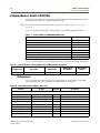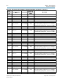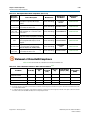
1
100G Development Kit, Stratix V GX Edition
Reference Manual
101 Innovation Drive
San Jose, CA 95134
www.altera.com
MNL-01066-1.1
Feedback Subscribe
© 2012 Altera Corporation. All rights reserved. ALTERA, ARRIA, CYCLONE, HARDCOPY, MAX, MEGACORE, NIOS, QUARTUS and STRATIX words and logos
are trademarks of Altera Corporation and registered in the U.S. Patent and Trademark Office and in other countries. All other words and logos identified as
trademarks or service marks are the property of their respective holders as described at www.altera.com/common/legal.html. Altera warrants performance of its
semiconductor products to current specifications in accordance with Altera's standard warranty, but reserves the right to make changes to any products and
services at any time without notice. Altera assumes no responsibility or liability arising out of the application or use of any information, product, or service
described herein except as expressly agreed to in writing by Altera. Altera customers are advised to obtain the latest version of device specifications before relying
on any published information and before placing orders for products or services.
August 2012
Altera Corporation
ISO
9001:2008
Registered
100G Development Kit, Stratix V GX Edition
Reference Manual
Contents
Chapter 1. Overview
General Description . . . . . . . . . . . . . . . . . . . . . . . . . . . . . . . . . . . . . . . . . . . . . . . . . . . . . . . . . . . . . . . . . . . . . 1–1
Development Board Block Diagram . . . . . . . . . . . . . . . . . . . . . . . . . . . . . . . . . . . . . . . . . . . . . . . . . . . . . . . . 1–3
Handling the Board . . . . . . . . . . . . . . . . . . . . . . . . . . . . . . . . . . . . . . . . . . . . . . . . . . . . . . . . . . . . . . . . . . . . . . 1–3
Chapter 2. Board Components
Introduction . . . . . . . . . . . . . . . . . . . . . . . . . . . . . . . . . . . . . . . . . . . . . . . . . . . . . . . . . . . . . . . . . . . . . . . . . . . . 2–1
Board Overview . . . . . . . . . . . . . . . . . . . . . . . . . . . . . . . . . . . . . . . . . . . . . . . . . . . . . . . . . . . . . . . . . . . . . . . . . 2–2
Featured Device: Stratix V GX FPGA . . . . . . . . . . . . . . . . . . . . . . . . . . . . . . . . . . . . . . . . . . . . . . . . . . . . . . . 2–6
I/O Resources . . . . . . . . . . . . . . . . . . . . . . . . . . . . . . . . . . . . . . . . . . . . . . . . . . . . . . . . . . . . . . . . . . . . . . . . 2–6
MAX II CPLD EPM2210 System Controller . . . . . . . . . . . . . . . . . . . . . . . . . . . . . . . . . . . . . . . . . . . . . . . . 2–11
Configuration, Status, and Setup Elements . . . . . . . . . . . . . . . . . . . . . . . . . . . . . . . . . . . . . . . . . . . . . . . . . 2–17
Configuration . . . . . . . . . . . . . . . . . . . . . . . . . . . . . . . . . . . . . . . . . . . . . . . . . . . . . . . . . . . . . . . . . . . . . . . 2–17
FPGA Programming over On-Board USB-Blaster II . . . . . . . . . . . . . . . . . . . . . . . . . . . . . . . . . . . . . 2–17
FPGA Programming from Flash Memory . . . . . . . . . . . . . . . . . . . . . . . . . . . . . . . . . . . . . . . . . . . . . 2–18
FPGA Programming over External USB-Blaster . . . . . . . . . . . . . . . . . . . . . . . . . . . . . . . . . . . . . . . . 2–18
Status Elements . . . . . . . . . . . . . . . . . . . . . . . . . . . . . . . . . . . . . . . . . . . . . . . . . . . . . . . . . . . . . . . . . . . . . . 2–19
Status LEDs . . . . . . . . . . . . . . . . . . . . . . . . . . . . . . . . . . . . . . . . . . . . . . . . . . . . . . . . . . . . . . . . . . . . . . . 2–19
Setup Elements . . . . . . . . . . . . . . . . . . . . . . . . . . . . . . . . . . . . . . . . . . . . . . . . . . . . . . . . . . . . . . . . . . . . . . 2–21
Board settings DIP switch . . . . . . . . . . . . . . . . . . . . . . . . . . . . . . . . . . . . . . . . . . . . . . . . . . . . . . . . . . . 2–21
Push Buttons . . . . . . . . . . . . . . . . . . . . . . . . . . . . . . . . . . . . . . . . . . . . . . . . . . . . . . . . . . . . . . . . . . . . . . 2–22
Board Jumpers . . . . . . . . . . . . . . . . . . . . . . . . . . . . . . . . . . . . . . . . . . . . . . . . . . . . . . . . . . . . . . . . . . . . 2–22
Clock Circuitry . . . . . . . . . . . . . . . . . . . . . . . . . . . . . . . . . . . . . . . . . . . . . . . . . . . . . . . . . . . . . . . . . . . . . . . . . 2–23
General User Input/Output . . . . . . . . . . . . . . . . . . . . . . . . . . . . . . . . . . . . . . . . . . . . . . . . . . . . . . . . . . . . . 2–26
User Push Buttons . . . . . . . . . . . . . . . . . . . . . . . . . . . . . . . . . . . . . . . . . . . . . . . . . . . . . . . . . . . . . . . . . . . 2–26
User DIP Switches . . . . . . . . . . . . . . . . . . . . . . . . . . . . . . . . . . . . . . . . . . . . . . . . . . . . . . . . . . . . . . . . . . . 2–27
User LEDs . . . . . . . . . . . . . . . . . . . . . . . . . . . . . . . . . . . . . . . . . . . . . . . . . . . . . . . . . . . . . . . . . . . . . . . . . . 2–28
LCD . . . . . . . . . . . . . . . . . . . . . . . . . . . . . . . . . . . . . . . . . . . . . . . . . . . . . . . . . . . . . . . . . . . . . . . . . . . . . . . . 2–29
Flash Memory . . . . . . . . . . . . . . . . . . . . . . . . . . . . . . . . . . . . . . . . . . . . . . . . . . . . . . . . . . . . . . . . . . . . . . . . . 2–30
Components and Interfaces . . . . . . . . . . . . . . . . . . . . . . . . . . . . . . . . . . . . . . . . . . . . . . . . . . . . . . . . . . . . . . 2–32
Transceiver Interfaces . . . . . . . . . . . . . . . . . . . . . . . . . . . . . . . . . . . . . . . . . . . . . . . . . . . . . . . . . . . . . . . . 2–32
QSFP Interface . . . . . . . . . . . . . . . . . . . . . . . . . . . . . . . . . . . . . . . . . . . . . . . . . . . . . . . . . . . . . . . . . . . . 2–33
SFP+ Interface . . . . . . . . . . . . . . . . . . . . . . . . . . . . . . . . . . . . . . . . . . . . . . . . . . . . . . . . . . . . . . . . . . . . . 2–35
CFP Interface . . . . . . . . . . . . . . . . . . . . . . . . . . . . . . . . . . . . . . . . . . . . . . . . . . . . . . . . . . . . . . . . . . . . . 2–37
Interlaken Interface . . . . . . . . . . . . . . . . . . . . . . . . . . . . . . . . . . . . . . . . . . . . . . . . . . . . . . . . . . . . . . . . 2–40
External Memory Interfaces . . . . . . . . . . . . . . . . . . . . . . . . . . . . . . . . . . . . . . . . . . . . . . . . . . . . . . . . . . . 2–44
DDR3 Interface . . . . . . . . . . . . . . . . . . . . . . . . . . . . . . . . . . . . . . . . . . . . . . . . . . . . . . . . . . . . . . . . . . . . 2–44
QDR II Interface . . . . . . . . . . . . . . . . . . . . . . . . . . . . . . . . . . . . . . . . . . . . . . . . . . . . . . . . . . . . . . . . . . . 2–55
Gigabit Ethernet Interface . . . . . . . . . . . . . . . . . . . . . . . . . . . . . . . . . . . . . . . . . . . . . . . . . . . . . . . . . . . . . 2–60
Heatsink and Fan . . . . . . . . . . . . . . . . . . . . . . . . . . . . . . . . . . . . . . . . . . . . . . . . . . . . . . . . . . . . . . . . . . . . . . . 2–62
Power . . . . . . . . . . . . . . . . . . . . . . . . . . . . . . . . . . . . . . . . . . . . . . . . . . . . . . . . . . . . . . . . . . . . . . . . . . . . . . . . 2–62
Power Distribution System . . . . . . . . . . . . . . . . . . . . . . . . . . . . . . . . . . . . . . . . . . . . . . . . . . . . . . . . . . . . 2–63
Power Measurement . . . . . . . . . . . . . . . . . . . . . . . . . . . . . . . . . . . . . . . . . . . . . . . . . . . . . . . . . . . . . . . . . 2–64
Statement of China-RoHS Compliance . . . . . . . . . . . . . . . . . . . . . . . . . . . . . . . . . . . . . . . . . . . . . . . . . . . . 2–65
August 2012
Altera Corporation
100G Development Kit, Stratix V GX Edition
Reference Manual
iv
Contents
Additional Information
Document Revision History . . . . . . . . . . . . . . . . . . . . . . . . . . . . . . . . . . . . . . . . . . . . . . . . . . . . . . . . . . . . . . 1–1
How to Contact Altera . . . . . . . . . . . . . . . . . . . . . . . . . . . . . . . . . . . . . . . . . . . . . . . . . . . . . . . . . . . . . . . . . . . 1–1
Typographic Conventions . . . . . . . . . . . . . . . . . . . . . . . . . . . . . . . . . . . . . . . . . . . . . . . . . . . . . . . . . . . . . . . . 1–1
100G Development Kit, Stratix V GX Edition
Reference Manual
August 2012 Altera Corporation
1. Overview
The 100G Development Kit, Stratix® V GX Edition allows you to evaluate the
performance of the Stratix V GX FPGA in a 100G design. This document provides the
detailed pin-out and component reference information required to create FPGA
designs that interface with all components on the board.
f For information about setting up the Stratix V GX 100G development board and using
the included software, refer to the 100G Development Kit, Stratix V GX Edition User
Guide.
General Description
The Stratix V GX 100G development board provides a hardware platform for
evaluating the performance and signal integrity features of the Altera® Stratix V GX
devices. The board features the following major component blocks:
■
■
622,000 logic elements (LEs)
■
50-Mbits (Mb) embedded memory
■
48 transceivers
■
210 full-duplex LVDS channels
■
28 phase locked loops (PLLs)
■
512 18x18-bit multipliers
■
840 user I/Os
■
2 PCI Express hard IP blocks
■
MAX® II 324-pin CPLD (EPM2210F324C3N)
■
FPGA configuration
■
August 2012
Stratix V GX FPGA (5SGXEA7N2F45C2N) in 1932-pin FineLine BGA® (FBGA)
package
■
MAX II CPLD and Flash Fast Passive Parallel (FPP) configuration
■
1-Gigabit (Gb) flash storage for two configuration images (factory and user)
■
On-board USB-BlasterTM II for use with the Quartus® II Programmer, Nios® II
software, and System Console
■
JTAG header for external USB-Blaster
Memory
■
Twelve 256-Mb DDR3 SDRAM devices
■
Two 72-Mb QDR II SRAM devices
■
Status and setup elements
■
FPGA clock sources
Altera Corporation
100G Development Kit, Stratix V GX Edition
Reference Manual
1–2
Chapter 1: Overview
General Description
■
Clock outputs and triggers
■
General user input/output
■
■
■
Seven user push buttons
■
Two user DIP switches
■
Eight user LEDs
■
Two-line character LCD
■
Ten configuration status LEDs
Components and interfaces
■
10/100/1000 Ethernet PHY and RJ-45 connector
■
USB 2.0 PHY
■
48 transceiver channels
■
Two channels for SMA interface
■
Four channels for SFP+ interface
■
Eight channels for Quad Small Form-factor Pluggable (QSFP) interface
■
10 channels for CFP interface
■
24 channels for Interlaken interface
Power
■
19-V DC input
■
2.5-mm barrel jack for DC power input
■
On/Off power slide switch
■
On-board power measurement circuitry
100G Development Kit, Stratix V GX Edition
Reference Manual
August 2012 Altera Corporation
Chapter 1: Overview
Development Board Block Diagram
1–3
Development Board Block Diagram
Figure 1–1 shows the block diagram of the Stratix V GX 100G development board.
Figure 1–1. Stratix V GX 100G Development Board Block Diagram
User LEDs,
Push Buttons
User LEDs,
Push Buttons
CFP
QSFP
QSFP
RJ45
Jack
64 MB
Flash
10/100/1000
Ethernet
Transceivers
Connected to
SMA Connectors
CPLD
(x32)
4 SFP+
Modules
On-Board
USB-Blaster
5SGXEA7N2F45C2
Interlaken
4 MB QDR II
(x18)
4 MB QDR II
(x36)
Clocks
& PLL
6 DDR3 SDRAM
(x32)
Handling the Board
When handling the board, it is important to observe the following static discharge
precaution:
c Without proper anti-static handling, the board can be damaged. Therefore, use
anti-static handling precautions when touching the board.
The Stratix V GX 100G development board must be stored between –40º C and 100º C.
The recommended operating temperature is between 0º C and 55º C.
August 2012
Altera Corporation
100G Development Kit, Stratix V GX Edition
Reference Manual
1–4
100G Development Kit, Stratix V GX Edition
Reference Manual
Chapter 1: Overview
Handling the Board
August 2012 Altera Corporation
2. Board Components
Introduction
This chapter introduces all the important components on the Stratix V GX 100G
development board. Figure 2–1 illustrates major component locations and Table 2–1
provides a brief description of all features of the board.
1
A complete set of schematics, a physical layout database, and GERBER files for the
development board reside in the Stratix V GX 100G development kit installation
directory.
f For information about powering up the board and installing the development kit
software, refer to the 100G Development Kit, Stratix V GX Edition User Guide.
This chapter consists of the following sections:
August 2012
■
“Board Overview” on page 2–2
■
“Featured Device: Stratix V GX FPGA” on page 2–6
■
“MAX II CPLD EPM2210 System Controller” on page 2–11
■
“Configuration, Status, and Setup Elements” on page 2–17
■
“Clock Circuitry” on page 2–23
■
“General User Input/Output” on page 2–26
■
“Flash Memory” on page 2–30
■
“Components and Interfaces” on page 2–32
■
“Power” on page 2–62
Altera Corporation
100G Development Kit, Stratix V GX Edition
Reference Manual
2–2
Chapter 2: Board Components
Board Overview
Board Overview
This section provides an overview of the Stratix V GX 100G development board,
including an annotated board image and component descriptions. Figure 2–1
provides an overview of the board features.
Figure 2–1. Overview of the Stratix V GX 100G Development Board Features
Interlaken Channel 12-23
(J54, J55)
DDR3 Memory
(U72-U83)
Stratix V GX FPGA
(U38)
QDR II SRAM
(U70, U71)
Interlaken Channel 0-11
(J52, J53)
Power
Switch
(SW1)
User DIP Switch
(SW5)
Clock Circuitry
FPGA User
Push Buttons
(S7-S10)
Power
Regulators
Character
LCD (J62)
Program Select
Push Button (S13)
DC Power
Jack (J1)
Reset Push Button
(S1)
Factory Push Button
(S15)
Load Push Button
(S14)
Board Settings
DIP Switch (SW4)
User DIP Switch
(SW6)
Auxiliary
Power
Jack (J2)
User Push Buttons
(S4-S6)
CPU Reset
Push Button (S3)
USB Type-B
Connector
(J65)
SFP Connectors (J45)
QSFP
Interface
(J65)
CFP
(J46)
JTAG
Ethernet Ethernet
QSFP
Interface Status LEDs RJ-45 Programming
(D12-D17) Connector Header
(J67)
(J7)
(J59)
Table 2–1 describes the components and lists their corresponding board references.
Table 2–1. Stratix V GX 100G Development Board Components (Part 1 of 4)
Board
Reference
Type
Description
Featured Device
U38
FPGA
5SGXEA7N2F45C2N Stratix V GX device in a 1932-pin FBGA package.
Configuration, Status, and Setup Elements
D24–D29,
D31–D34
Configuration status LEDs
100G Development Kit, Stratix V GX Edition
Reference Manual
Indicates the FPP configuration status.
August 2012 Altera Corporation
Chapter 2: Board Components
Board Overview
2–3
Table 2–1. Stratix V GX 100G Development Board Components (Part 2 of 4)
Board
Reference
Type
Description
D1
Power LED
Indicates the board power status.
D20-D23
Ethernet status LEDs
Indicates the Ethernet connection speed as well as transmit or receive activity.
D31
Factory POF LED
Illuminates when the factory design is being loaded into the FPGA.
D32
Load LED
Illuminates when the FPGA is being configured.
D24
Error LED
Illuminates when the FPGA configuration from flash fails.
D25
Configuration done LED
Illuminates when the FPGA is successfully configured.
J62
MAX_JTAG_EN jumper
Bypasses the MAX II CPLD EPM2210 System Controller in the JTAG chain when
shunted.
J59
JTAG programming header
JTAG programming header for connecting an Altera USB-Blaster dongle to
program the FPGA and MAX II CPLD devices.
J65
JTAG for on-board
USB-Blaster II
JTAG for on-board USB-Blaster MAX II CPLD device programming.
S1
CPU reset push button
Resets the FPGA logic.
S7
Reset push button
Resets the MAX II CPLD EPM2210 System Controller logic.
S8
PGM_SEL push button
Selects which design file to load into the FPGA.
S5
Load push button
Initiates loading of the FPGA.
S6
Factory push button
Initiates loading of factory design into the FPGA.
Board settings DIP switch
Controls the MAX II CPLD EPM2210 System Controller functions such as clock
enable, power and temperature monitor, as well as voltage settings for
transceivers and SMA clock input control.
U59
MAX II CPLD (System)
Altera EPM2210F324C3N, MAX II CPLD for MAX II+FPP configuration.
U62
MAX II CPLD (On-Board
USB-Blaster II)
Altera EPM570GF100, MAX II CPLD for on-board USB-Blaster II circuitry.
SW3
Clock Circuitry
J41, J50
LVDS differential clock input to I/O bank 3.
J17, J21
LVDS reference clock input for the optical interfaces
J18, J22
LVDS reference clock input for Stratix V GX device for the optical interfaces.
J43, J52
SMA input clocks
Center LVDS reference clock inputs for the Interlaken interface.
J46, J55
Outer LVDS reference clock inputs for the Interlaken interface.
J20, J23
LVDS reference clock input for upper 12 bits of the Interlaken interface.
J58, J63
LVDS reference clock input for lower 12 bits of the Interlaken interface.
J42, J51
Differential SMA clock output for I/O bank 3.
J11, J14
Reference SMA clock output for the optical interfaces.
J12, J15
SMA output clock divided for the CFP interface.
J8, J13
644.53125 MHz LVDS clock.
J44, J53
SMA output clocks
LVDS SMA output clock for the Interlaken interface.
J45, J54
LVDS SMA output clock for the Interlaken interface.
J47, J56
LVDS SMA output clock for the Interlaken interface.
J5, J6
SMA output clock from upper 12 bits of the Interlaken interface.
J27, J28
SMA output clock from lower 12 bits of the Interlaken interface.
August 2012
Altera Corporation
100G Development Kit, Stratix V GX Edition
Reference Manual
2–4
Chapter 2: Board Components
Board Overview
Table 2–1. Stratix V GX 100G Development Board Components (Part 3 of 4)
Board
Reference
Type
Description
U20
LVPECL to LVDS buffer
644.53125MHz LVDS clock buffer.
U47, U48,
U49
Differential to LVDS clock
buffer
Differential clock buffer (2 to 4) distributed to CMU and dedicated differential
clock inputs on the vertical banks of the FPGA.
U21
Differential divide-by-4
clock divider
Divide-by-4 clock circuit to provide the required clock to CFP.
U30
Differential to LVDS clock
buffer
Differential clock buffer (2 to 6) distributed to CMU of the FPGA and to clock
dividers for the optical clock.
U44, U22,
U53
External programmable
PLLs
On-board programmable PLL clock source with buffers.
X1
644.53125-MHz LVPECL
oscilator
644.53-MHz clock to the FPGA transceivers.
X2
100-MHz oscillator
100-MHz oscillator for the MAX II device’s PFL function.
X3
25-MHz oscillator
25-MHz oscillator for the Ethernet controller.
X4
125-MHz oscillator
125-MHz oscillator for the Ethernet interface.
X5
50-MHz oscillator
50-MHz NIOS II CPU clock (CMOS).
Y1, Y2, Y3
25-MHz crystal clock
25-MHz reference clock for external PLLs.
General User Input and Output
D39–D42
User LEDs
Four green LEDs for the MAX II CPLD EPM2210 System Controller.
D43–D50
FPGA LEDs
Eight green LEDs for the FPGA.
J64
Character LCD
Connector which interfaces to the 16 character × 2 line LCD module.
S2–S4
User push buttons
User push buttons that connect to the MAX II CPLD EPM2210 System Controller.
S9–S12
FPGA user push buttons
User push buttons that connect to the Stratix V GX device.
SW4
Bank-of-eight user DIP
switch
User DIP switch that connects to the FPGA.
SW5
Bank-of-eight user DIP
switch
User DIP switch that connects to the MAX II CPLD EPM2210 System Controller.
Memory Devices
U24-U29,
U31-U36
DDR3 x32 port
Twelve 256-Mb independent DDR3 memory with 16-bit data bus, combining to
make six 32-bit DDR3 interface.
U40
QDR II x18 port
One 72-Mb independent QDR II memory with 18-bit data bus.
U41
QDR II x36 port
One 72-Mb independent QDR II memory with 36-bit data bus.
U60
Flash memory
Synchronous burst mode flash device which provides 1-Gb non-volatile memory.
This device is located under the character LCD.
Components and Interfaces
J33
QSFP interface
QSFP XCVR interface (4 channels): QSFP0_TX_P/_N[3:0], QSFP0_RX_P/_N[3:0]
J19
QSFP interface
QSFP XCVR interface (4 channels): QSFP1_TX_P/_N[3:0], QSFP1_RX_P/_N[3:0]
J25
CFP interface
CFP XCVR interface (10 channels): CFP_TX_P/_N[9:0], CFP_RX_P/_N[9:0]
J10
SFP+ interface
Four SFP+ XCVR interfaces.
J61
I/O connector
General purpose expansion connector with 10 user-definable I/Os that connect to
the MAX II CPLD EPM2210 System Controller.
100G Development Kit, Stratix V GX Edition
Reference Manual
August 2012 Altera Corporation
Chapter 2: Board Components
Board Overview
2–5
Table 2–1. Stratix V GX 100G Development Board Components (Part 4 of 4)
Board
Reference
Type
Description
J4, J16,
J38, J60
Interlaken interface
Interlaken interface (24 channels).
U50
10/100/1000 Ethernet PHY Marvell 88E1111 triple speed Ethernet PHY.
J57
Ethernet RJ-45 connector
Halo HFJ11-1G02E RJ-45 connector with integrated magnetic that provides a
10/100/1000 Ethernet connection via a Marvell 88E1111 PHY and the
FPGA-based Altera Triple Speed Ethernet MegaCore function in RGMII mode.
J5
USB type-B connector
For type-B USB cable connection to program the FPGA using JTAG on-board
USB-Blaster II.
U63
USB PHY
FT245BL USB PHY device for configuring the FPGA using on-board
USB-Blaster II.
DC power jack
19-V DC power jack.
Power switch
Switch to power on or off the board when power is supplied from the DC power
input jack.
U9, U10
Dual 5-V switcher
Supplies 5-V power to the dual switcher and other regulators for biasing.
U13
2.5-V switcher
Supplies 2.5-V power to VCCIO, VCCPD, VCC_CLKIN, and VCC_PGM on the
FPGA.
U11, U12
Dual 1.5-V switcher
Supplies 1.5-V power to the VCCIO on the FPGA and external memory.
U7
3.3-V switcher
Supplies 3.3-V power.
U19
12-V switcher
Supplies 12-V power.
U15-U18
Quad 0.9-V swither
Supplies 0.9-V power to the FPGA core and VCCHIP.
U77
1.5-V linear regulator
Supplies 1.5-V power to VCCPT on the FPGA.
U65
2.5-V switcher
Supplies 2.5-V power to VCC_AUX and VCCA on the FPGA.
U70
1.6-V linear regulator
Supplies 1.6-V power to the VCCH_GXB on the FPGA.
U67
1.2-V linear regulator
Supplies 1.2-V power to the VCCT_GXB on the FPGA.
Power
J2
SW1
U69
1.2-V linear regulator
Supplies 1.2-V power to the VCCR_GXB on the FPGA.
U71, U75
ADC 8/16 channel 24-bit
Monitors the current of all FPGA power rails.
U72, U76
4.25-V linear regulator
Supplies 4.25-V power for the current monitor circuit.
U37
3.3-V linear regulator
Supplies 3.3-V power to the VCCA_GXB on the FPGA.
U73
0.9-V linear regulator
Supplies 0.9 V power to VCCD on the FPGA.
U54, U45,
U23
3.3-V linear regulator
Supplies 3.3-V power to the external PLLs.
U46
1.1-V linear regulator
Supplies 1.1-V power to the 10/100/1000 Ethernet PHY.
U43
LM95235 temperature
sensor
Monitors the FPGA temperature.
U8
5-V switcher
Supplies 5-V power to the optical regulators.
U66
3.3-V linear regulator
Supplies 3.3-V power to QSFP and SFP+.
U74
1.8-V linear regulator
Supplies 1.8-V power to QDR II VDD.
U78
1.2-V linear regulator
Supplies 1.2-V power to the translator device for CFP.
U64, U80,
U79
0.75-V VTT/VREF regulator Supplies 0.75-V VTT/VREF to external memories and termination.
August 2012
Altera Corporation
100G Development Kit, Stratix V GX Edition
Reference Manual
2–6
Chapter 2: Board Components
Featured Device: Stratix V GX FPGA
Featured Device: Stratix V GX FPGA
The Stratix V GX 100G development board features the 5SGXEA7N2F45C2N Stratix V
GX FPGA device (U38) in a 1932-pin FBGA package.
f For more information about the Stratix V GX devices, refer to the Stratix V Device
Handbook.
Table 2–2 describes the features of the Stratix V GX 5SGXEA7N2F45C2N device.
Table 2–2. Stratix V GX Device 5SGXEA7N2F45C2N Features
Features
Total
Equivalent LEs
622,000
M20K Memory Blocks (2048 × 72 bits)
2,560
M20K Memory (Mbits)
50
Total Transceiver Channels
48
18-bit × 18-bit Multipliers
512
27-bit × 27-bit Multipliers
256
PLLs
28
Maximum User I/O pins
840
Table 2–3 lists the Stratix V GX component reference and manufacturing information.
Table 2–3. Stratix V GX Device Component Reference and Manufacturing Information
Board Reference
U38
Manufacturer
Manufacturing
Part Number
Manufacturer
Website
Altera Corporation
5SGXEA7N2F45C2N
www.altera.com
Description
Stratix V GX F1932, Lead Free
I/O Resources
Table 2–4 summarizes the FPGA I/O usage by function on the Stratix V GX 100G
development board. The I/O direction is with respect to the FPGA.
Table 2–4. Stratix V GX I/O Usage Summary (Part 1 of 6)
Function
I/O Type
I/O Count
Description
REFCLK_CAP_QL0
2.5-V LVDS input
2
Differential REFCLK input
REFCLK_CAP_QL1
2.5-V LVDS input
2
Differential REFCLK input
REFCLK_CAP_QL2
2.5-V LVDS input
2
Differential REFCLK input
REFCLK_CAP_QL3
2.5-V LVDS input
2
Differential REFCLK input
REFCLK_CAP_QR0
2.5-V LVDS input
2
Differential REFCLK input
REFCLK_CAP_QR1
2.5-V LVDS input
2
Differential REFCLK input
REFCLK_CAP_QR2
2.5-V LVDS input
2
Differential REFCLK input
REFCLK_CAP_QR3
2.5-V LVDS input
2
Differential REFCLK input
REFCLKB_CAP_QL0
2.5-V LVDS input
2
Differential REFCLK input
FPGA Transceiver Clocks
100G Development Kit, Stratix V GX Edition
Reference Manual
August 2012 Altera Corporation
Chapter 2: Board Components
Featured Device: Stratix V GX FPGA
2–7
Table 2–4. Stratix V GX I/O Usage Summary (Part 2 of 6)
Function
I/O Type
I/O Count
Description
REFCLKB_CAP_QL2
2.5-V LVDS input
2
Differential REFCLK input
PRGCLK_QL1
2.5-V LVDS input
2
Differential REFCLK input
SMA_REFCLK_CAP
2.5-V LVDS input
2
Differential REFCLK input
FPGA Global Clocks
CLKIN_125
2.5-V LVDS input
2
Global clock
CLKIN_50_FPGA
2.5-V LVCMOS input
1
Global clock
DDR3A_CLK_IN
2.5-V LVDS input
2
Differential global clock
DIFFCLK_IN1
2.5-V LVDS input
2
Differential global clock
QDR2A_CLK_IN
2.5-V LVDS input
2
Differential global clock
QDR2B_CLK_IN
2.5-V LVDS input
2
Differential global clock
VCXOB_CLK_IN
2.5-V LVDS input
2
Differential global clock
SMA_IN
2.5-V LVCMOS input
1
SMA clock input
SMA_OUT
2.5-V LVCMOS output
1
SMA clock output
SMA_RX_P/_N[1:0]
Transceiver
non-inverted/inverted input
4
SMA receive channel
SMA_TX_P/_N[1:0]
Transceiver
non-inverted/inverted output
4
SMA transmit channel
2.5-V LVCMOS output
1
Flash advance input
SMA Transceivers
Flash
FLASH_ADVN
FLASH_CEN
2.5-V LVCMOS output
1
Flash chip enable
FLASH_CLK
2.5-V LVCMOS output
1
Flash clock
FLASH_OEN
2.5-V LVCMOS output
1
Flash output enable
FLASH_RDYBSYN
2.5-V LVCMOS output
1
Flash ready
FLASH_RESETN
2.5-V LVCMOS output
1
Flash reset
FLASH_WEN
2.5-V LVCMOS output
1
Flash write enable
FSM_A[25:1]
2.5-V LVCMOS output
25
Flash address bus
FSM_D[15:0]
2.5-V LVCMOS bidirectional
16
Flash data bus
DDR3_RZQIN
1.5-V
1
DDR3
DDR3_A[13:0]
1.5-V SSTL output
14
DDR3 address
DDR3_BA[2:0]
1.5-V SSTL output
3
DDR3 bank address
Diff 1.5-V SSTL input
4
DDR3 data strobe
1.5-V SSTL bidirectional
32
DDR3 data
1.5-V SSTL output
1
DDR3 clock enable
Diff 1.5-V SSTL input
2
DDR3 clock
DDR3 SDRAM (Six each)
DDR3_DQS_P/_N[3:0]
DDR3_DQ[31:0]
DDR3_CKE
DDR3_CK_P/_N
DDR3_CASN
1.5-V SSTL output
1
DDR3 chip select
DDR3_WEN
1.5-V SSTL output
1
DDR3 write enable
DDR3_RASN
1.5-V SSTL output
1
DDR3 RAS#
August 2012
Altera Corporation
100G Development Kit, Stratix V GX Edition
Reference Manual
2–8
Chapter 2: Board Components
Featured Device: Stratix V GX FPGA
Table 2–4. Stratix V GX I/O Usage Summary (Part 3 of 6)
Function
I/O Type
I/O Count
Description
DDR3_CASN
1.5-V SSTL output
1
DDR3 CAS#
DDR3_RSTN
1.5-V SSTL output
1
DDR3 reset
DDR3_ODT
1.5-V SSTL output
1
DDR3 on-die termination
QDR II SRAM (x36)
QDR2A_RZQIN
1.5-V
1
QDR II
QDR2A_A[19:0]
1.5-V HSTL output
20
QDR II address
QDR2A_Q[35:0]
1.5-V HSTL input
36
QDR II data output
QDR2A_D[35:0]
1.5-V HSTL output
36
QDR II data input
QDR2A_BWSN[3:0]
1.5-V HSTL output
4
QDR II byte write select
QDR2A_WPSN
1.5-V HSTL output
1
QDR II write port select
QDR2A_RPSN
1.5-V HSTL output
1
QDR II read port select
QDR2A_K_P/_N
1.5-V HSTL output
2
QDR II clock input
QDR2A_CQ_P/_N
1.5-V HSTL output
2
QDR II echo clock
QDR2B_A[20:0]
1.5-V HSTL output
21
QDR II address
QDR2B_Q[17:0]
1.5-V HSTL input
18
QDR II data output
QDR2B_D[17:0]
1.5-V HSTL output
18
QDR II data input
QDR2B_BWSN[1:0]
1.5-V HSTL output
2
QDR II byte write select
QDR2B_WPSN
1.5-V HSTL output
1
QDR II write port select
QDR2B_RPSN
1.5-V HSTL output
1
QDR II read port select
QDR2B_K_P/_N
1.5-V HSTL output
2
QDR II clock input
QDR2B_CQ_P/_N
1.5-V HSTL output
2
QDR II echo clock
QSFP_RX_P/_N[3:0]
Transceiver
non-inverted/inverted input
4
QSFP receive channel
QSFP_TX_P/_N[3:0]
Transceiver
non-inverted/inverted output
4
QSFP transmit channel
QSFP_MOD_SELN
2.5-V LVCMOS output
1
QSFP module select
QSFP_RST
2.5-V LVCMOS output
1
QSFP reset
QSFP_SCL
2.5-V LVCMOS output
1
QSFP serial two-wire clock
QSFP_SDA
2.5-V LVCMOS bidirectional
1
QSFP serial two-wire data
QSFP_INTERRUPTN
2.5-V LVCMOS output
1
QSFP interrupt
QSFP_MOD_PRSN
2.5-V LVCMOS input
1
QSFP module present
QSFP_LP_MODE
2.5-V LVCMOS output
1
QSFP low power mode
SFP_RD_P/_N
Transceiver
non-inverted/inverted input
2
SFP+ receive channel
SFP_TD_P/_N
Transceiver
non-inverted/inverted output
2
SFP+ transmit channel
QDR II SRAM (x18)
QSFP (Two each)
SFP+ (Four each)
100G Development Kit, Stratix V GX Edition
Reference Manual
August 2012 Altera Corporation
Chapter 2: Board Components
Featured Device: Stratix V GX FPGA
2–9
Table 2–4. Stratix V GX I/O Usage Summary (Part 4 of 6)
Function
I/O Type
I/O Count
SFP_TXDISABLE
2.5-V LVCMOS output
1
SFP+ transmitter disable
SFP_RATESEL
2.5-V LVCMOS output
1
SFP+ rate select
SFP_MOD_PRSNTN
2.5-V LVCMOS input
1
SFP+ module present
2.5-V CMOS input
2
SFP+ module absent
SFP_SCL
2.5-V LVCMOS output
1
SFP+ serial two-wire clock
SFP_SDA
2.5-V LVCMOS bidirectional
1
SFP+ serial two-wire data
SFP_TXFAULT
2.5-V LVCMOS input
1
SFP+ transmitter fault
SFP_LOS
2.5-V LVCMOS input
1
SFP+ loss of signal
CFP_RX_P/_N[9:0]
Transceiver input
20
CFP receive channel
CFP_TX_P/_N[9:0]
Transceiver output
20
CFP transmit channel
2.5-V LVCMOS output
3
CFP programmable control I/O
CFP_MDC
2.5-V LVCMOS output
1
CFP management data I/O clock
CFP_MDIO
2.5-V LVCMOS bidirectional
1
CFP management data I/O data
CFP_MOD_RST
2.5-V LVCMOS output
1
CFP module reset
CFP_TX_DIS
2.5-V LVCMOS output
1
CFP transmitter disable
CFP_RX_LOS
2.5-V LVCMOS input
1
CFP loss of signal
CFP_PRG_ALRM[3:1]
2.5-V LVCMOS input
3
CFP programmable alarm
CFP_GLB_ALRM
2.5-V LVCMOS input
1
CFP global alarm
CFP_MOD_LOPWR
2.5-V LVCMOS output
1
CFP low power mode
CFP_MOD_ABS
2.5-V LVCMOS input
1
CFP module absent
INT_CAP_RX_P/_N[23:0]
Transceiver
non-inverted/inverted input
48
Interlaken receive channel
INT_TX_P/_N[23:0]
Transceiver
non-inverted/inverted output
48
Interlaken transmit channel
INT_LSB_CON_RX_FC_CK
2.5-V LVCMOS input
1
Interlaken reference clock input (LSB)
INT_LSB_CON_RX_FC_DATA
2.5-V LVCMOS input
1
Interlaken reference clock data (LSB)
SFP_MOD_ABS
Description
CFP
CFP_PRG_CNTL[3:1]
Interlaken
INT_LSB_CON_RX_FC_SYNC
2.5-V LVCMOS input
1
Interlaken reference clock sync (LSB)
INT_LSB_CON_TX_FC_CK
2.5-V LVCMOS output
1
Interlaken reference clock output (LSB)
INT_LSB_CON_TX_FC_DATA
2.5-V LVCMOS output
1
Interlaken reference clock data (LSB)
INT_LSB_CON_TX_FC_SYNC
2.5-V LVCMOS output
1
Interlaken reference clock sync (LSB)
INT_MSB_CON_RX_FC_CK
2.5-V LVCMOS input
1
Interlaken reference clock input (MSB)
INT_MSB_CON_RX_FC_DATA
2.5-V LVCMOS input
1
Interlaken reference clock data (MSB)
INT_MSB_CON_RX_FC_SYNC
2.5-V LVCMOS input
1
Interlaken reference clock sync (MSB)
INT_MSB_CON_TX_FC_CK
2.5-V LVCMOS output
1
Interlaken reference clock output (MSB)
INT_MSB_CON_TX_FC_DATA
2.5-V LVCMOS output
1
Interlaken reference clock data (MSB)
INT_MSB_CON_TX_FC_SYNC
2.5-V LVCMOS output
1
Interlaken reference clock sync (MSB)
MAX II Bridge Control
August 2012
Altera Corporation
100G Development Kit, Stratix V GX Edition
Reference Manual
2–10
Chapter 2: Board Components
Featured Device: Stratix V GX FPGA
Table 2–4. Stratix V GX I/O Usage Summary (Part 5 of 6)
Function
I/O Type
I/O Count
Description
MAX2_CLK
2.5-V LVCMOS output
1
FPGA flash control
MAX2_OEN
2.5-V LVCMOS output
1
MAX II output enable
MAX2_WEN
2.5-V LVCMOS output
1
MAX II write enable
MAX2_CSN
2.5-V LVCMOS output
1
MAX II chip select
USB_ADDR[1:0]
1.5-V output
2
USB-Blaster II address
USB_CLK
1.5-V output
1
USB-Blaster II clock
1.5-V bidirectional
8
USB-Blaster II data
USB_EMPTY
1.5-V input
1
USB-Blaster II empty
USB_FULL
1.5-V input
1
USB-Blaster II full
USB_OEN
1.5-V output
1
USB-Blaster II output enable
USB_RDN
1.5-V output
1
USB-Blaster II ready
USB_RESETN
1.5-V output
1
USB-Blaster II reset
USB_SCL
1.5-V output
1
USB-Blaster II two-wire clock
USB_SDA
1.5-V bidirectional
1
USB-Blaster II two-wire data
USB_WRN
1.5-V output
1
USB-Blaster II write enable
FPGA DCLK
2.5-V LVCMOS input
1
FPP clock
FPGA DATA[7:0]
2.5-V LVCMOS input
8
FPP data
FPGA_MSEL[4:0]
2.5-V LVCMOS input
5
Dedicated configuration pins
FPGA_CONFIGN
2.5-V LVCMOS
1
Dedicated configuration pins
FPGA_STATUSN
2.5-V LVCMOS output
1
Dedicated configuration pins
FPGA_CEN
2.5-V LVCMOS input
1
Dedicated configuration pins
FPGA_NIO_PULLUP
2.5-V LVCMOS input
1
Dedicated configuration pins
FPGA_CONF_DONE
2.5-V LVCMOS output
1
Dedicated configuration pins
FPGA_JTAG_TCK
2.5-V LVCMOS input
1
FPP JTAG chain clock
FPGA_JTAG_TDO
2.5-V LVCMOS
1
FPP JTAG chain data out
FPGA_JTAG_TMS
2.5-V LVCMOS input
1
FPP JTAG chain mode
FPGA_JTAG_TRST
2.5-V LVCMOS input
1
FPP JTAG chain reset
2.5-V LVCMOS
1
MAX II CPLD on-board JTAG chain data out
CPU_RESET
2.5-V LVCMOS input
1
Nios® II CPU reset push button
USER_RESET
2.5-V LVCMOS input
1
User reset push button
FPGA_USER_DIPSW[7:0]
2.5-V LVCMOS input
8
8 user DIP switches
FPGA_USER_LED[7:0]
2.5-V LVCMOS input
8
8 user LEDs
FPGA_USER_PB[3:0]
2.5-V LVCMOS input
4
4 user push buttons
LCD_CSN
2.5-V LVCMOS output
1
LCD chip select
LCD_D_CN
2.5-V LVCMOS output
1
LCD data or control signal
LCD_DATA[7:0]
2.5-V LVCMOS output
8
LCD data
On-Board USB-Blaster II
USB_DATA[7:0]
FPP Configuration
JTAG_BLASTER_TDO
User I/O
100G Development Kit, Stratix V GX Edition
Reference Manual
August 2012 Altera Corporation
Chapter 2: Board Components
MAX II CPLD EPM2210 System Controller
2–11
Table 2–4. Stratix V GX I/O Usage Summary (Part 6 of 6)
Function
I/O Type
I/O Count
2.5-V LVCMOS output
1
LCD write enable
ENET_TXD[3:0]
2.5-V LVCMOS output
4
Ethernet transmit RGMII data bus
ENET_TX_EN
2.5-V LVCMOS output
1
Ethernet transmit enable
ENET_GTX_CLK
2.5-V LVCMOS output
1
Ethernet transmit clock
ENET_RXD[3:0]
2.5-V LVCMOS input
4
Ethernet receive RGMII data bus
ENET_RX_DV
2.5-V LVCMOS input
1
Ethernet receive data valid
ENET_RX_CLK
2.5-V LVCMOS input
1
Ethernet receive clock
ENET_INTN
2.5-V LVCMOS input
1
Ethernet management bus interrupt
ENET_MDC
2.5-V LVCMOS output
1
Ethernet RGMII clock
ENET_MDIO
2.5-V LVCMOS bidirectional
1
Ethernet RGMII data
2.5-V LVCMOS output
1
Ethernet reset
LCD_WEN
Description
Ethernet
ENET_RESETN
1020
Total I/O:
MAX II CPLD EPM2210 System Controller
The board utilizes the EPM2210 System Controller, an Altera MAX II CPLD, for the
following purposes:
August 2012
■
FPGA configuration from flash memory
■
Power consumption monitoring
■
Temperature monitoring
■
Virtual JTAG interface for PC-based power and temperature GUI
■
Control registers for clocks
■
Control registers for Remote System Update
■
Control registers for general purpose I/O and PFL
■
Register with CPLD design revision and board information (read-only)
Altera Corporation
100G Development Kit, Stratix V GX Edition
Reference Manual
2–12
Chapter 2: Board Components
MAX II CPLD EPM2210 System Controller
Figure 2–2 illustrates the MAX II CPLD EPM2210 System Controller's functionality
and external circuit connections.
Figure 2–2. MAX II CPLD EPM2210 System Controller Block Diagram
PC
JTAG Control
On-Board
USB-Blaster II
SLD-HUB
FSM BUS
Information
Register
Encoder
Decoder
Virtual-JTAG
Control
Register
Temperature
Measure
Results
LM95235
Controller
Power
Measure
Results
LTC2418
Controller
Si5338
Programmable
Oscillator
Si5338
Controller
FPGA
FLASH
PFL
GPIO
Fast Configuration
Downloader
MAX II CPLD
Table 2–5 lists the I/O signals present on the MAX II CPLD EPM2210 System
Controller. The signal names and functions are relative to the MAX II device (U59).
Table 2–5. MAX II CPLD EPM2210 System Controller Device Pin-Out (Part 1 of 5)
Board
Reference
(U59)
Schematic Signal
Name
I/O
Standard
Stratix V GX
Device Pin
Number
Pin Description
R18
CLK125_EN
2.5-V
—
125-MHz oscillator clock enable
D16
CLK50_EN
2.5-V
—
50-MHz oscillator clock enable
D2
CLK_1588_SEL
2.5-V
—
Programmable VCXO enable signal for the clock to FPGA
bank 3B
C2
CLK_SFP_SEL
2.5-V
—
Programmable VCXO enable signal for the clock to FPGA
bank QR1
J6
CLKIN_50_MAX
2.5-V
—
50-MHz oscillator clock enable
H17
CONFIGN_LED
2.5-V
—
FPGA initialization LED
J1
CSENSE_SCK
2.5-V
—
Power monitor SPI clock
H6
CSENSE_SDI
2.5-V
—
Power monitor SPI input data
K1
CSENSE_SDO
2.5-V
—
Power monitor SPI output data
R12
EXTRA_SIG0
1.5-V
—
Extra signal
V14
EXTRA_SIG1
1.5-V
—
Extra signal
P12
EXTRA_SIG2
1.5-V
—
Extra signal
100G Development Kit, Stratix V GX Edition
Reference Manual
August 2012 Altera Corporation
Chapter 2: Board Components
MAX II CPLD EPM2210 System Controller
2–13
Table 2–5. MAX II CPLD EPM2210 System Controller Device Pin-Out (Part 2 of 5)
Board
Reference
(U59)
Schematic Signal
Name
I/O
Standard
Stratix V GX
Device Pin
Number
Pin Description
M3
FACTORY
2.5-V
—
Push button to load factory image into the FPGA
M4
FACTORY_POF
2.5-V
—
LED to Indicate that factory Programmer Object File (.pof)
is loaded into the FPGA
V15
FACTORY_REQUEST
1.5-V
—
On-board USB-Blaster II request to send FACTORY
command
R13
FACTORY_STATUS
1.5-V
—
On-board USB-Blaster II FACTORY command status
A9
FLASH_ADVN
2.5-V
AE34
FSM bus flash address valid
D9
FLASH_CEN
2.5-V
AD14
FSM bus flash chip enable
E9
FLASH_OEN
2.5-V
AV8
FSM bus flash output enable
B9
FLASH_RDYBSYN
2.5-V
AU20
FSM bus flash ready
F9
FLASH_RESETN
2.5-V
AE32
FSM bus flash reset
A8
FLASH_WEN
2.5-V
AJ11
FSM bus flash write enable
B15
FPGA_CONF_DONE
2.5-V
AH9
FPGA configuration done
A15
FPGA_CONFIGN
2.5-V
AM38
Initiates new image to the FPGA
B18
FPGA_DATA0
2.5-V
BB38
FPGA configuration data
D14
FPGA_DATA1
2.5-V
BD38
FPGA configuration data
A17
FPGA_DATA2
2.5-V
BC39
FPGA configuration data
E13
FPGA_DATA3
2.5-V
BD37
FPGA configuration data
B16
FPGA_DATA4
2.5-V
BC38
FPGA configuration data
D13
FPGA_DATA5
2.5-V
AR37
FPGA configuration data
C15
FPGA_DATA6
2.5-V
AP37
FPGA configuration data
F12
FPGA_DATA7
2.5-V
AN39
FPGA configuration data
C14
FPGA_DCLK
2.5-V
AG36
FPGA configuration clock
R4
FPGA_JTAG_TCK
2.5-V
AL34
FPGA on-board JTAG chain clock
M7
FPGA_JTAG_TDO
2.5-V
AL36
FPGA on-board JTAG chain data out
E12
FPGA_STATUSN
2.5-V
AL8
FPGA configuration error
E11
FSM_A1
2.5-V
AR10
FSM bus flash address
B14
FSM_A2
2.5-V
AJ10
FSM bus flash address
B13
FSM_A3
2.5-V
AV20
FSM bus flash address
A12
FSM_A4
2.5-V
AN37
FSM bus flash address
A13
FSM_A5
2.5-V
BD7
FSM bus flash address
C13
FSM_A6
2.5-V
AL12
FSM bus flash address
C12
FSM_A7
2.5-V
AJ34
FSM bus flash address
D10
FSM_A8
2.5-V
AR11
FSM bus flash address
A7
FSM_A9
2.5-V
BD34
FSM bus flash address
B6
FSM_A10
2.5-V
AG19
FSM bus flash address
B7
FSM_A11
2.5-V
AW11
FSM bus flash address
C7
FSM_A12
2.5-V
AT11
FSM bus flash address
August 2012
Altera Corporation
100G Development Kit, Stratix V GX Edition
Reference Manual
2–14
Chapter 2: Board Components
MAX II CPLD EPM2210 System Controller
Table 2–5. MAX II CPLD EPM2210 System Controller Device Pin-Out (Part 3 of 5)
Board
Reference
(U59)
Schematic Signal
Name
I/O
Standard
Stratix V GX
Device Pin
Number
Pin Description
A5
FSM_A13
2.5-V
AE29
FSM bus flash address
B5
FSM_A14
2.5-V
AW22
FSM bus flash address
A4
FSM_A15
2.5-V
AN36
FSM bus flash address
A6
FSM_A16
2.5-V
AW9
FSM bus flash address
B3
FSM_A17
2.5-V
AT36
FSM bus flash address
B11
FSM_A18
2.5-V
BA21
FSM bus flash address
E8
FSM_A19
2.5-V
AJ12
FSM bus flash address
C8
FSM_A20
2.5-V
AD33
FSM bus flash address
C11
FSM_A21
2.5-V
AF34
FSM bus flash address
B8
FSM_A22
2.5-V
AH33
FSM bus flash address
C4
FSM_A23
2.5-V
AT20
FSM bus flash address
B4
FSM_A24
2.5-V
AJ33
FSM bus flash address
A2
FSM_A25
2.5-V
AW36
FSM bus flash address
B1
FSM_A26
2.5-V
BC20
FSM bus flash address
E10
FSM_D0
2.5-V
AG9
FSM bus flash data
A14
FSM_D1
2.5-V
AG11
FSM bus flash data
F10
FSM_D2
2.5-V
AY33
FSM bus flash data
F11
FSM_D3
2.5-V
BD35
FSM bus flash data
C5
FSM_D4
2.5-V
AV37
FSM bus flash data
D7
FSM_D5
2.5-V
AV35
FSM bus flash data
F7
FSM_D6
2.5-V
AL9
FSM bus flash data
C6
FSM_D7
2.5-V
AF13
FSM bus flash data
D11
FSM_D8
2.5-V
AP9
FSM bus flash data
B12
FSM_D9
2.5-V
AJ32
FSM bus flash data
F8
FSM_D10
2.5-V
AT33
FSM bus flash data
E7
FSM_D11
2.5-V
AK9
FSM bus flash data
D8
FSM_D12
2.5-V
AN38
FSM bus flash data
D5
FSM_D13
2.5-V
AJ21
FSM bus flash data
D6
FSM_D14
2.5-V
BC10
FSM bus flash data
E6
FSM_D15
2.5-V
BB36
FSM bus flash data
H13
INIT_DONE_LED
2.5-V
—
FPGA initialization done LED. Indicates that the FPGA is in
user mode.
N6
JTAG_MAX_TDO
2.5-V
—
MAX II CPLD on-board JTAG chain data out
P5
MAX_JTAG_TMS
2.5-V
—
MAX II CPLD on-board JTAG chain mode
H1
LCD_CSN
2.5-V
BA22
LCD display chip select
G7
LCD_D_CN
2.5-V
AR12
LCD data or control signal
G6
LCD_DATA0
2.5-V
BB39
LCD data
H2
LCD_DATA1
2.5-V
AR21
LCD data
100G Development Kit, Stratix V GX Edition
Reference Manual
August 2012 Altera Corporation
Chapter 2: Board Components
MAX II CPLD EPM2210 System Controller
2–15
Table 2–5. MAX II CPLD EPM2210 System Controller Device Pin-Out (Part 4 of 5)
Board
Reference
(U59)
Schematic Signal
Name
I/O
Standard
Stratix V GX
Device Pin
Number
Pin Description
G5
LCD_DATA2
2.5-V
AV11
LCD data
H3
LCD_DATA3
2.5-V
AF31
LCD data
G4
LCD_DATA4
2.5-V
AE12
LCD data
G1
LCD_DATA5
2.5-V
BD20
LCD data
F6
LCD_DATA6
2.5-V
AP31
LCD data
G2
LCD_DATA7
2.5-V
AU11
LCD data
J3
LCD write enable
LCD_WEN
2.5-V
AM32
N17
LINE_SIDE0
2.5-V
—
M13
LINE_SIDE1
2.5-V
—
N18
LINE_SIDE2
2.5-V
—
M12
LINE_SIDE3
2.5-V
—
M16
LINE_SIDE4
2.5-V
—
L16
LINE_SIDE5
2.5-V
—
M17
LINE_SIDE6
2.5-V
—
Spare I/Os on the MAX II CPLD and function as an I/O
expander for the FPGA. Data can pass through the MAX II
CPLD to the Stratix V GX interface.
L15
LINE_SIDE7
2.5-V
—
M18
LINE_SIDE8
2.5-V
—
L14
LINE_SIDE9
2.5-V
—
M5
LOAD
2.5-V
—
Initiates a load of the selected image from the PFL
U16
M570_CLOCK
1.5-V
—
25-MHz clock to on-board USB-Blaster II for sending the
FACTORY command
G12
MAX2_CLK
2.5-V
AW10
MAX II CPLD clock
F17
MAX2_CSN
2.5-V
AG10
MAX II CPLD chip select
F18
MAX2_OEN
2.5-V
AY37
MAX II CPLD output enable
G13
MAX2_WEN
2.5-V
AN12
MAX II CPLD write enable
T16
MAX_CONF_DONEN
2.5-V
—
FPGA configuration done LED. Indicates that the FPGA is
loaded with the new image.
T17
MAX_ERROR
2.5-V
—
FPGA configuration error LED
R15
MAX_LOAD
2.5-V
—
FPGA configuration active LED
C17
OVERTEMPN
2.5-V
—
Over-temperature indicator from the temperature sense
circuit
N1
PGM_SEL
2.5-V
—
Push button to select which image to program into the
FPGA
P3
PHASE60
2.5-V
—
Switch control for the dual 1.5-V and 3.3-V regulators
P2
PHASE120
2.5-V
—
Switch control for the dual 5.0-V and 2.5-V regulators
P4
PHASE180
2.5-V
—
Switch control for the dual 5.0-V and 2.5-V regulators
P1
PHASE240
2.5-V
—
Switch control for the dual 1.5-V and 3.3-V regulators
N4
PWR_CTL
2.5-V
—
Power monitor control
H5
SENSE_CE0
2.5-V
—
Chip select for the first current sense ADC
J2
SENSE_CE1
2.5-V
—
Chip select for the second current sense ADC
August 2012
Altera Corporation
100G Development Kit, Stratix V GX Edition
Reference Manual
2–16
Chapter 2: Board Components
MAX II CPLD EPM2210 System Controller
Table 2–5. MAX II CPLD EPM2210 System Controller Device Pin-Out (Part 5 of 5)
Board
Reference
(U59)
Schematic Signal
Name
I/O
Standard
Stratix V GX
Device Pin
Number
Pin Description
J15
SI5338_PLL_SCL
2.5-V
AT21
Si5338 serial two-wire clock for transceiver PLL
J17
SI5338_PLL_SDA
2.5-V
AJ19
Si5338 serial two-wire data for transceiver PLL
G18
STATUSN_LED
2.5-V
—
Status indicator for programming the FPGA
E15
TSENSE_SMB_CLK
2.5-V
—
Temperature sense clock
C16
TSENSE_SMB_DATA
2.5-V
—
Temperature sense data
J13
USB_CLK
1.5-V
AP10
On-board USB-Blaster II clock
V2
USB_CFG0
1.5-V
BC17
On-board USB-Blaster II data
R5
USB_CFG1
1.5-V
BA19
On-board USB-Blaster II data
U3
USB_CFG2
1.5-V
BB23
On-board USB-Blaster II data
P6
USB_CFG3
1.5-V
AT26
On-board USB-Blaster II data
T4
USB_CFG4
1.5-V
BB24
On-board USB-Blaster II data
R6
USB_CFG5
1.5-V
AT17
On-board USB-Blaster II data
U4
USB_CFG6
1.5-V
BD19
On-board USB-Blaster II data
T6
USB_CFG7
1.5-V
AN23
On-board USB-Blaster II data
N3
USER1_POF
2.5-V
—
N5
USER2_POF
2.5-V
—
N2
USER3_POF
2.5-V
—
E16
USER_DIPSW0
2.5-V
—
User DIP switch
F14
USER_DIPSW1
2.5-V
—
User DIP switch
D18
USER_DIPSW2
2.5-V
—
User DIP switch
F13
USER_DIPSW3
2.5-V
—
User DIP switch
E17
USER_DIPSW4
2.5-V
—
User DIP switch
G15
USER_DIPSW5
2.5-V
—
User DIP switch
E18
USER_DIPSW6
2.5-V
—
User DIP switch
G14
USER_DIPSW7
2.5-V
—
User DIP switch
C10
USER_LED0
2.5-V
—
User LED
A11
USER_LED1
2.5-V
—
User LED
C9
USER_LED2
2.5-V
—
User LED
B10
USER_LED3
2.5-V
—
User LED
E14
USER_PB0
2.5-V
—
User push button
D17
USER_PB1
2.5-V
—
User push button
F15
USER_PB2
2.5-V
—
User push button
F16
USER_PB3
2.5-V
—
User push button
100G Development Kit, Stratix V GX Edition
Reference Manual
LED to Indicate which user .pof file is loaded into the FPGA
August 2012 Altera Corporation
Chapter 2: Board Components
Configuration, Status, and Setup Elements
2–17
Table 2–6 lists the MAX II CPLD EPM2210 System Controller component reference
and manufacturing information.
Table 2–6. MAX II CPLD EPM2210 System Controller Component Reference and Manufacturing Information
Board
Reference
Description
Manufacturer
Manufacturing
Part Number
Manufacturer
Website
U59
MAX II CPLD EPM2210 324FBGA -3
Altera Corporation
EPM2210F324C3N
www.altera.com
Configuration, Status, and Setup Elements
This section describes the board’s configuration, status, and setup elements.
Configuration
The Stratix V GX development board supports three configuration methods:
■
On-board USB-Blaster II is the default method for configuring the FPGA at any
time using the Quartus II Programmer in JTAG mode with the supplied USB cable.
■
MAX II+Flash Fast Passive Parallel (FPP) download for configuring the FPGA
using stored images from flash memory on either a power-up or by pressing the
LOAD or FACTORY push button (S5).
■
JTAG programming header (J59) for configuring the FPGA using an external
USB-Blaster (not supplied) and the Quartus II Programmer.
The following sections describe each of these methods.
FPGA Programming over On-Board USB-Blaster II
The USB-Blaster II is implemented using a USB type-B connector (J5), a USB 2.0 PHY
device, and an Altera MAX II CPLD EPM570GF100 (U62). This allows configuration
of the FPGA using a USB cable that connects directly between the USB port on the
board (J5) and a USB port of a PC running the Quartus II software. The on-board
USB-Blaster II normally masters the JTAG chain. The on-board USB-Blaster II
automatically disables when you connect an external USB-Blaster to the JTAG chain at
the JTAG programming header (J59).
Figure 2–3 shows a block diagram for the FPGA programming over on-board
USB-Blaster II.
Figure 2–3. FPGA Programming over On-Board USB-Blaster II
JTAG
JTAG Programming
Header
USB Type-B
Connector
August 2012
USB
Altera Corporation
USB PHY
USB FIFO BUS EPM570F100
MAX II
CPLD
JTAG
Stratix V GX
FPGA
100G Development Kit, Stratix V GX Edition
Reference Manual
2–18
Chapter 2: Board Components
Configuration, Status, and Setup Elements
FPGA Programming from Flash Memory
On either power-up or by pressing the LOAD or FACTORY push button (S5 or S6), the
MAX II CPLD System Controller’s parallel flash loader configures the FPGA from the
flash memory. The configuration program select push-button, PGM_SEL, (S8) selects
between two .pof files (factory or user) stored in the flash. The MAX II CPLD System
Controller uses the Altera Parallel Flash Loader (PFL) megafunction to configure the
FPGA by reading data from the flash and converting it to FPP format. This data is
then written to the FPGA’s dedicated configuration pins during configuration.
Figure 2–4 shows the block diagram for the MAX II+Flash FPP configuration.
Figure 2–4. MAX II+Flash FPP Configuration
FPP Configuration
LOAD/FACTORY
Push Button
MAX II
CPLD
Flash
Stratix V GX
FPGA
MAX_ERROR LED
USER_POF LED
FACTORY_POF LED
Flash
PGM_SEL
Push Button
Flash
Memory
Additionally, ten green configuration status LEDs (D24–D29 and D31–D34) indicate
the FPP configuration status. After configuration completes, you can determine which
.pof image is loaded into the FPGA by observing the FACTORY_POF LED (D31) or the
USER1_POF, USER2_POF, USER3_POF LEDs (D34, D33, D32).
f For more information on the flash map storage, refer to the 100G Development Kit,
Stratix V GX Edition User Guide.
FPGA Programming over External USB-Blaster
The JTAG programming header provides another method for configuring the FPGA
using an external USB-Blaster device with the Quartus II Programmer running on a
PC. The MAX II JTAG configuration jumper allows you to remove the MAX II CPLD
from the JTAG chain so that the FPGA is the only device on the chain.
100G Development Kit, Stratix V GX Edition
Reference Manual
August 2012 Altera Corporation
Chapter 2: Board Components
Configuration, Status, and Setup Elements
2–19
Figure 2–5 shows the schematic connections for the dedicated JTAG programming
header (J59).
Figure 2–5. JTAG Programming Header
Jumper to remove
the MAX II CPLD from
JTAG programming header
JTAG
Programming Header
TDI
9
TMS
5
TCK
1
3
Stratix V GX
MAX II CPLD
S4GT_TDI
S4GT_TDO
JTAG_TMS
MAX_FPP_TDI MAX_FPP_TDO
JTAG_TCK
JTAG_TMS
JTAG_TCK
LAST_TDO
Status Elements
The development board include board-specific status LEDs and switches for enabling
and configuring various features on the board, as well as a 16 character × 2 line LCD
for displaying board power and temperature measurements. This section describes
the status and setup elements.
Status LEDs
Surface mount LEDs indicate the various status of the board. A logic 0 is driven on the
I/O port to turn on the LED while a logic 1 is driven to turn off the LED.
Table 2–7 lists the LED board references, names, and functional descriptions.
Table 2–7. Status LEDs (Part 1 of 2)
Board
Reference
LED Name
Schematic
Signal Name
I/O Standard
LED Description
—
—
Blue LED. Illuminates when the board power switch
(SW1) is on. Driven by the 3.3-V regulator.
ENET_LED_DUPLEX
2.5-V CMOS
Green LED. Illuminates to indicate Ethernet full
duplex status. Driven by the Marvell 88E1111 PHY.
D1
Power
D20
DUPLEX
D21
1000
ENET_LED_LINK1000
Green LED. Illuminates to indicate Ethernet linked
2.5-V CMOS at 1000-Mbps connection speed. Driven by the
Marvell 88E1111 PHY.
D22
100
ENET_LED_LINK100
Green LED. Illuminates to indicate Ethernet linked
2.5-V CMOS at 100-Mbps connection speed. Driven by the
Marvell 88E1111 PHY.
D23
10
ENET_LED_LINK10
Green LED. Illuminates to indicate Ethernet linked
2.5-V CMOS at 10-Mbps connection speed. Driven by the
Marvell 88E1111 PHY.
August 2012
Altera Corporation
100G Development Kit, Stratix V GX Edition
Reference Manual
2–20
Chapter 2: Board Components
Configuration, Status, and Setup Elements
Table 2–7. Status LEDs (Part 2 of 2)
Board
Reference
LED Name
Schematic
Signal Name
I/O Standard
LED Description
D18
TX
ENET_LED_TX
Green LED. Blinks to indicate Ethernet PHY
2.5-V CMOS transmit activity. Driven by the Marvell 88E1111
PHY.
D19
RX
ENET_LED_RX
2.5-V CMOS
D34,
User1 POF
USER1_POF
D33,
User2 POF
USER2_POF
D32
User3 POF
USER3_POF
D31
Factory POF
FACTORY_POF
D26
MAX_LOAD
MAX_LOAD
D25
MAX_CONF_DN
Green LED. Blinks to indicate Ethernet PHY receive
activity. Driven by the Marvell 88E1111 PHY.
Green LED. Illuminates when the user .pof image is
2.5-V CMOS to be programmed into the FPGA.
2.5-V CMOS
Green LED. Illuminates when the factory .pof image
is successfully programmed into the FPGA.
Green LED. Illuminates when the MAX II CPLD is
2.5-V CMOS actively configuring the FPGA. Driven by the MAX II
System Controller CPLD.
MAX_CONF_DONEn
2.5-V CMOS
Green LED. Illuminates when the FPGA is
successfully configured. Driven by the FPGA.
Red LED. Illuminates when the MAX II CPLD
EPM2210 System Controller fails to configure the
2.5-V CMOS
FPGA. Driven by the MAX II CPLD EPM2210
System Controller.
D24
MAX_ERR
D27
INIT DN
INIT_DONE_LED
2.5-V CMOS
Green LED. Illuminates when the FPGA is initialized
and in user mode.
D28
CONFIG
CONFIGn_LED
2.5-V CMOS
Green LED. Illuminates when the FPGA is
configured and is loaded with the new image.
D29
STATUSn
STATUSn_LED
2.5-V CMOS
Green LED. Illuminates when the FPGA is being
programmed.
D30
OVERTEMPn
MAX_ERROR
OVERTEMPn
Green LED. Illuminates when a heat sink or fan
2.5-V CMOS should be installed. Driven by the MAX1619
thermal sensor OVERTEMPn signal.
Table 2–8 lists the board-specific LEDs component references and manufacturing
information.
Table 2–8. Status LEDs Component References and Manufacturing Information
Board Reference
Device
Description
Manufacturer
D19–D23, D25–D34,
D39–D50
Green LEDs
D11, D14, D15, D16
Green LEDs
D17, D24
Red LED
D1
Blue LED
Lumex Inc.
100G Development Kit, Stratix V GX Edition
Reference Manual
Lumex Inc.
Manufacturer
Part Number
Manufacturer
Website
SML-LX1206GC-TR
www.lumex.com
Lumex Inc.
SML-LXT0805GW-TR
www.lumex.com
Lumex Inc.
SML-LX1206IC-TR
www.lumex.com
SML-LX1206USBC-TR
www.lumex.com
August 2012 Altera Corporation
Chapter 2: Board Components
Configuration, Status, and Setup Elements
2–21
Setup Elements
The development board includes several different kinds of setup elements. This
section describes the following setup elements:
■
Board settings DIP switch
■
Push buttons
■
Board jumpers
Board settings DIP switch
The board settings DIP switch (SW3) controls various features specific to the board
and the MAX II CPLD EPM2210 System Controller logic design.
Table 2–9 lists the board settings DIP switch controls and descriptions.
Table 2–9. Board Settings DIP Switch Controls
Board Reference
(SW3)
Schematic Signal
Name
USB_DISABLEn
1
I/O
Standard
2.5-V
DIFFCLKA_SEL
2
2.5-V
REFCLKA_SEL
3
2.5-V
DIFFCLKB_SEL
4
2.5-V
REFCLKB_SEL
5
CLK644_EN
6
2.5-V
2.5-V
SECURITY
7
2.5-V
Settings
(1)
1: Enabled
Description
Disables the on-board USB-Blaster II.
0: Disabled
1: SMA input
0: PLL input
1: SMA input
0: PLL input
1: SMA input
0: PLL input
1: SMA input
Selects SMA or PLL for the differential clock that
goes to the global clock inputs of clock A tree
structure.
Selects SMA or PLL that goes to the transceivers
of clock A tree structure.
Selects SMA or PLL for the differential clock that
goes to the global clock inputs of clock B tree
structure.
0: PLL input
Selects SMA or PLL that goes to the transceivers
of clock B tree structure.
1: Enabled
Enables the 644.53125-MHz clock.
0: Disabled
1: Enabled
0: Disabled
Turns on configuration security. When enabled,
the FPGA cannot be accessed via JTAG if the
device has already been programmed by the PFL.
Note to Table 2–9:
(1) When the switch is in the OFF position, a logic 1 is selected while in the ON position, a logic 0 is selected.
Table 2–10 lists the board settings DIP switch component reference and
manufacturing information.
Table 2–10. Board Settings DIP Switch Component References and Manufacturing Information
Board
Reference
SW3
August 2012
Device Description
DIP switch
Altera Corporation
Manufacturer
Grayhill Corporation
Manufacturer
Part Number
Manufacturer Website
76SB08ST
www.grayhill.com
100G Development Kit, Stratix V GX Edition
Reference Manual
2–22
Chapter 2: Board Components
Configuration, Status, and Setup Elements
Push Buttons
Board reference S1 is the CPU reset push button, CPU_RESET, which is an input to the
Stratix V GX device. The CPU_RESET is the master reset signal for the FPGA design
loaded into the Stratix V GX device. You must enable the CPU_RESET signal within the
Quartus II software for this reset function to work. Otherwise, the CPU_RESET acts as a
regular I/O pin. When you enable this signal in the Quartus II software, and then set
to logic 1 on the board, this push button resets every register within the FPGA.
Board reference S7 is the reset push button, RESET, which is an input to the MAX II
CPLD EPM2210 System Controller. This reset signal is the default reset for the CPLD
logic. This signal forces a FPGA reconfiguration from the flash memory.
Board references S5, S6, and S8 are push buttons for MAX II+Flash FPP configuration.
Use the PGM_SEL push button (S8) to select the configuration programming image
stored in the flash memory.
Table 2–11 lists the push buttons references, names, and functional descriptions.
Table 2–11. Push Buttons Signal Names and Functions
Board
Reference
Schematic Signal
Name
I/O Standard
Description
S1
CPU_RESET
2.5-V
Reset signal for the FPGA and MAX II CPLD EPM2210 System
Controller.
S5
LOAD
2.5-V
Initiates loading of the FPGA.
S6
FACTORY
2.5-V
Initiates loading of factory design into the FPGA.
S7
RESET
2.5-V
User reset signal for the MAX II CPLD EPM2210 System Controller.
S8
PGM_SEL
2.5-V
Selects between two .pof files (factory or user) stored in the flash.
Table 2–12 lists the push buttons component references and the manufacturing
information.
Table 2–12. Push-Buttons Component References and Manufacturing Information
Board Reference
S1, S5–S8
Device Description
Push buttons
Manufacturer
Manufacturer
Part Number
Manufacturer
Website
Panasonic Corporation
EVQPAC07K
www.panasonic.com
Board Jumpers
The board jumpers control feature specific to the JTAG chain and the MAX II CPLD
EPM2210 System Controller logic design. Table 2–13 lists the board jumper references,
names, and functional descriptions.
Table 2–13. Board Jumpers
Board
Reference
Schematic
Signal Name
J62
MAX_JTAG_EN
J9
FAN BYPASS
Description
■
Jumper installed – includes the MAX II CPLD device (U59) in the JTAG programming chain.
■
Jumper removed – removes the MAX II CPLD device (U59) from the JTAG programming
chain.
■
Jumper installed – fan is always on.
■
Jumper removed – MAX II CPLD EPM2210 System Controller controls the fan speed.
100G Development Kit, Stratix V GX Edition
Reference Manual
August 2012 Altera Corporation
Chapter 2: Board Components
Clock Circuitry
2–23
Clock Circuitry
The clock tree structure for the line side and QDRII interface on the Stratix V GX
board is made up of two programmable quad PLLs where each output can be
programmed for a specific frequency. The default frequency for the clocks going to
QL0 through QL3 is 644.53125 MHz and the default frequency going to the QDRII
interface is 100 MHz.
Figure 2–6 shows the Stratix V GX development board clock tree structure for the line
side and QDRII interface.
Figure 2–6. Development Board Clock Tree Structure for Line Side and QDRII Interface
SMA
LVDS
Clock Buffer
MUX
SMA
REFCLK_QR3
PLL
644.53125 MHz
REFCLK_QL1
SMA
SMA
Si571
ICS8543
100 MHz
125 MHz
PLL
PLL
1588
644.53125 MHz
25 MHz
Si5338
LVDS
Clock Buffer
MUX
SMA
SMA
REFCLK_QR0
REFCLK_QR1
REFCLK_QR2
REFCLK_QR3
Optical Clock
ICS8543
644.53125 MHz
Divide-by-4
Differential
Clock
CFP
SMA
SMA
SMA
LVDS
Clock
Buffer
Si571
MC100ES6139
SMA
SMA
SMA
NB6L11SMNG
50MHZ_MAX_II
Clock
Buffer
50MHZ_STRATIX
50 MHz
100 MHz
100 MHz
PLL
644.53125 MHz
25 MHz
644.53125 MHz
QDRII_CLK
QDRII_CLK
REFCLK_QR0
REFCLK_QR2
Si5338
SMA
SMA
REFCLK_QR3
The clock tree structure for the Interlaken interface and the DDR3 interface uses one
programmable on-board quad PLL to generate the necessary frequencies. The default
frequency for the Interlaken interface is 625 MHz and for the DDR3 interface is
100 MHz.
August 2012
Altera Corporation
100G Development Kit, Stratix V GX Edition
Reference Manual
2–24
Chapter 2: Board Components
Clock Circuitry
Figure 2–7 shows the Stratix V GX development board clock tree structure for the
Interlaken side and DDR3 interface.
Figure 2–7. Stratix V GX Development Board Clock Tree Structure for Interlaken Side and DDR3 Interface
SMA
LVDS
Clock Buffer
MUX
SMA
100 MHz
DDR3_CLK
625 MHz
ICS8543
REFCLK_QR1
REFCLK_QR2
SMA
SMA
SMA
SMA
SMA
PLL
Interlaken
x12
SMA
Interlaken
x12
SMA
SMA
SMA
625 MHz
25 MHz
Si5338
LVDS
Clock Buffer
MUX
SMA
SMA
ICS8543
REFCLK_QR0
REFCLK_QR3
SMA
SMA
SMA
SMA
SMA
You can select between the PLL or an off-board clock for the clock distribution path by
using the board settings DIP switch (SW3). This DIP switch is located near the bottom
left corner of the board. Refer to Table 2–9 on page 2–21 for the switch settings and
descriptions. The DIP switch with USB_DISABLEn label connects to the MAX II device
and controls the traffic that passes through the USB connector.
Table 2–14 lists the clock signal names, I/O standards, and functional descriptions.
Table 2–14. Clock Circuitry Pin-Out (Part 1 of 2)
Schematic
Signal Name
I/O
Standard
Stratix V GX Device
Pin Name
DIFFCLK_IN1_N/P
LVDS
BA34/AY34
Differential programmable clock to I/O bank 3B.
CLKIN_125_N/P
LVDS
BA18/AY18
Differential fixed clock to I/O bank 3B for Ethernet.
REFCLK_QL0_N/P
LVDS
AK6/AK7
Differential programmable clock to reference clock for the
transceivers that go to the optical interfaces.
REFCLKB_QL0_N/P
LVDS
AH5/AH6
Differential programmable clock to reference clock for the
transceivers that go to the optical interfaces.
REFCLK_QL1_N/P
LVDS
AF6/AF7
Differential programmable clock to reference clock for the
transceivers that go to the optical interfaces.
REFCLK_QL2_N/P
LVDS
AB5/AB6
Differential programmable clock to reference clock for the
transceivers that go to the optical interfaces.
REFCLKB_QL2_N/P
LVDS
Y6/Y7
Differential programmable clock to reference clock for the
transceivers that go to the optical interfaces.
REFCLK_QL3_N/P
LVDS
V5/V6
Differential programmable clock to reference clock for the
transceivers that go to the optical interfaces.
SMA_REFCLK_N/P
LVDS
T6/T7
Reference clock SMA input to transceivers that go to the
optical interfaces.
PRGCLK_QL1_N/P
LVDS
AD5/AD6
Differential programmable clock to reference clock for the
transceivers that go to the optical interfaces.
CFP_REFCLK_N/P
CML
—
100G Development Kit, Stratix V GX Edition
Reference Manual
Description
Divide-by-four differential programmable clock to the
reference clock for the CFP interface.
August 2012 Altera Corporation
Chapter 2: Board Components
Clock Circuitry
2–25
Table 2–14. Clock Circuitry Pin-Out (Part 2 of 2)
Schematic
Signal Name
I/O
Standard
Stratix V GX Device
Pin Name
Description
REFCLK_QR0_N/P
LVDS
AK39/AK38
Differential programmable clock to reference clock for the
transceivers that go to the Interlaken interface.
REFCLK_QR1_N/P
LVDS
AF39/AF38
Differential programmable clock to reference clock for the
transceivers that go to the Interlaken interface.
REFCLK_QR2_N/P
LVDS
AB40/AB39
Differential programmable clock to reference clock for the
transceivers that go to the Interlaken interface.
REFCLK_QR3_N/P
LVDS
V40/V39
Differential programmable clock to reference clock for the
transceivers that go to the Interlaken interface.
QDR2A_CLK_IN_N/P
LVDS
BB27/BA27
Differential programmable clock to the FPGA fabric for the
QDRII interface.
QDR2B_CLK_IN_N/P
LVDS
BD8/BC8
Differential programmable clock to the FPGA fabric for the
QDRII interface.
VCXOB_CLK_IN_N/P
LVDS
BC34/BB33
Differential programmable clock to I/O bank 3B for 1588.
DDR3A_CLK_IN_N/P
LVDS
F16/G16
Differential programmable clock to the FPGA fabric for the
DDR3 interface.
SMA_DIFF_CLKIN_N/P0
LVDS
—
SMA input to FPGA reference clocks for the FPGA fabric.
REFCLK_OSC_N/P
LVDS
—
SMA input to FPGA reference clocks for transceivers to
optical interfaces.
SMA_REF_CLKIN_N/P
LVDS
—
SMA input to FPGA reference clocks for transceivers to
Interlaken interface.
SMA_DIFF_CLKIN_N/P1
LVDS
—
SMA input to FPGA reference clocks for transceivers to
Interlaken interface.
BUFFB_CLK_N/P
LVDS
—
SMA buffered output of reference clocks distribute to
transceivers for Interlaken interface.
REFCLK_QL_N/P
LVDS
—
SMA buffered output of reference clocks distributed to
transceivers for optical interfaces.
OPTIC_CLK_N/P
LVDS
—
SMA buffered output of divide-by-four clock distributed to
the CFP optical interface.
BUFFA_DIFF_CLK_N/P
LVDS
—
SMA buffered output to clocks distributed to FPGA fabric.
BUFFA_REF_CLK0_N/P
LVDS
—
SMA buffered output of reference clocks distribute to
transceivers for Interlaken interface.
BUFFA_REF_CLK1_N/P
LVDS
—
SMA buffered output of reference clocks distribute to
transceivers for Interlaken interface.
CLK_644_N/P
LVDS
—
644.53125 MHz SMA output clock.
CLK_CONFIG
2.5-V
LVCMOS
—
100 MHz clock that goes to the MAX II System Controller
for the PFL.
CLKIN_50_FPGA
2.5-V
LVCMOS
AY9
50 MHz clock that goes to the Stratix V GX and MAX II
System Controller.
August 2012
Altera Corporation
100G Development Kit, Stratix V GX Edition
Reference Manual
2–26
Chapter 2: Board Components
General User Input/Output
General User Input/Output
This section describes the user I/O interface to the FPGA and MAX II CPLD EPM2210
System Controller, including the following elements:
■
User push buttons
■
User DIP switches
■
User LEDs
■
LCD
Figure 2–8 shows the general user I/O connection.
Figure 2–8. General User I/O Connection
MAX II
CPLD
4 User
LEDs
Stratix V GX
FPGA
User DIP
Switch
8 FPGA 4 User
User LEDs Push
Buttons
3 User Push
Buttons
User DIP
Switch
User Push Buttons
The development board includes seven push buttons for user-defined logic input and
one CPU reset. For information on the CPU reset push button, refer to “Push Buttons”
on page 2–22.
Board references S2 to S4 and S9 to S12 are push buttons that allow you to interact
with the MAX II CPLD device and the Stratix V GX device. When you press the
switch and hold it down, the device pin is set to logic 0. When you release the switch,
the device pin is set to logic 1. There is no board-specific function for these general
user push buttons.
Table 2–15 lists the user push button schematic signal names and their corresponding
Stratix V GX device pin numbers.
Table 2–15. User Push Button Signal Names and Functions (Part 1 of 2)
Board
Reference
Schematic
Signal Name
I/O Standard
Stratix V GX Device
Pin Number
Description
S2
USER_PB2
2.5-V CMOS
—
MAX II user push button
S3
USER_PB1
2.5-V CMOS
—
MAX II user push button
100G Development Kit, Stratix V GX Edition
Reference Manual
August 2012 Altera Corporation
Chapter 2: Board Components
General User Input/Output
2–27
Table 2–15. User Push Button Signal Names and Functions (Part 2 of 2)
Board
Reference
Schematic
Signal Name
I/O Standard
Stratix V GX Device
Pin Number
—
MAX II user push button
S4
USER_PB0
2.5-V CMOS
Description
S9
FPGA_USER_PB3
2.5-V CMOS
AM23
FPGA user push button
S10
FPGA_USER_PB2
2.5-V CMOS
AW23
FPGA user push button
S11
FPGA_USER_PB1
2.5-V CMOS
AR24
FPGA user push button
S12
FPGA_USER_PB0
2.5-V CMOS
AU25
FPGA user push button
Table 2–23 lists the user push-button switch component reference and the
manufacturing information.
Table 2–16. User Push-Button Switch Component References and Manufacturing Information
Board
Reference
S2–S4,
S9–S12
Device Description
Push buttons
Manufacturer
Manufacturer
Part Number
Manufacturer Website
Panasonic Corporation
EVQPAC07K
www.panasonic.com
User DIP Switches
Board references SW4 and SW5 are an 8-pin DIP switch with numbering marked on it
to indicate the switch number. When the switch is in the ON position, a logic 1 is
selected. When the switch is in the OFF position, a logic 0 is selected. The switches are
user-defined and provide additional FPGA input control. There is no board-specific
function for these switches.
Table 2–17 lists the user-defined DIP switch schematic signal names and their
corresponding Stratix V GX pin numbers.
Table 2–17. User-Defined DIP Switch Schematic Signal Names and Functions
Board
Reference
Schematic
Signal Name
I/O Standard
Stratix V GX Device
Pin Number
SW5.1
USER_DIPSW0
2.5-V CMOS
—
SW5.2
USER_DIPSW1
2.5-V CMOS
—
SW5.3
USER_DIPSW2
2.5-V CMOS
—
SW5.4
USER_DIPSW3
2.5-V CMOS
—
SW5.5
USER_DIPSW4
2.5-V CMOS
—
SW5.6
USER_DIPSW5
2.5-V CMOS
—
SW5.7
USER_DIPSW6
2.5-V CMOS
—
SW5.8
USER_DIPSW7
2.5-V CMOS
—
August 2012
Altera Corporation
Description
User-defined DIP switch that connects to
the MAX II CPLD device.
100G Development Kit, Stratix V GX Edition
Reference Manual
2–28
Chapter 2: Board Components
General User Input/Output
Table 2–17. User-Defined DIP Switch Schematic Signal Names and Functions
Board
Reference
Schematic
Signal Name
I/O Standard
Stratix V GX Device
Pin Number
AG12
SW4.1
FPGA_USER_DIPSW0
2.5-V CMOS
SW4.2
FPGA_USER_DIPSW1
2.5-V CMOS
BC7
SW4.3
FPGA_USER_DIPSW2
2.5-V CMOS
AE13
SW4.4
FPGA_USER_DIPSW3
2.5-V CMOS
AG21
SW4.5
FPGA_USER_DIPSW4
2.5-V CMOS
AY22
SW4.6
FPGA_USER_DIPSW5
2.5-V CMOS
AU9
SW4.7
FPGA_USER_DIPSW6
2.5-V CMOS
AM31
SW4.8
FPGA_USER_DIPSW7
2.5-V CMOS
AF35
Description
User-defined DIP switch that connects to
the FPGA device.
Table 2–18 lists the component references and the manufacturing information.
Table 2–18. Component Reference Input and Ouput Devices
Board Reference
SW4, SW5
Manufacturer
Manufacturer
Part Number
Manufacturer Website
Grayhill Corporation
76SB08ST
www.grayhill.com
Device Description
DIP switches
User LEDs
This section describes all user-defined LEDs. For information on board specific or
status LEDs, refer to“Status Elements” on page 2–19.
Board references D39 through D42 and D43 through D49 are 12 user LEDs that allow
status and debugging signals to be driven to the LEDs from the designs loaded into
the Stratix V GX device. The LEDs illuminate when a logic 0 is driven, and turns off
when a logic 1 is driven. There is no board-specific function for these LEDs.
Table 2–19 lists the user-defined LED schematic signal names and their corresponding
Stratix V GX pin numbers.
Table 2–19. User-Defined LED Schematic Signal Names and Functions (Part 1 of 2)
Board
Reference
Schematic
Signal Name
I/O Standard
Stratix V GX Device
Pin Number
D39
USER_LED3
2.5-V CMOS
—
D40
USER_LED2
2.5-V CMOS
—
D41
USER_LED1
2.5-V CMOS
—
D42
USER_LED0
2.5-V CMOS
—
100G Development Kit, Stratix V GX Edition
Reference Manual
Description
General-purpose green surface mount
(type 1206) user LEDs.
August 2012 Altera Corporation
Chapter 2: Board Components
General User Input/Output
2–29
Table 2–19. User-Defined LED Schematic Signal Names and Functions (Part 2 of 2)
Board
Reference
Schematic
Signal Name
I/O Standard
Stratix V GX Device
Pin Number
D43
FPGA_USER_LED7
2.5-V CMOS
AY19
D44
FPGA_USER_LED6
2.5-V CMOS
D36
D45
FPGA_USER_LED5
2.5-V CMOS
AN17
D46
FPGA_USER_LED4
2.5-V CMOS
AV23
D47
FPGA_USER_LED3
2.5-V CMOS
AK18
D48
FPGA_USER_LED2
2.5-V CMOS
AN14
D49
FPGA_USER_LED1
2.5-V CMOS
AT27
D50
FPGA_USER_LED0
2.5-V CMOS
AU27
Description
General-purpose green surface mount
(type 1206) user LEDs.
Table 2–23 lists the component references and the manufacturing information.
Table 2–20. Component Reference Input and Ouput Devices
Board Reference
D39––D50
Device
Description
Green LEDs
Manufacturer
Part Number
Manufacturer
Lumex Inc.
Manufacturer Website
SML-LX1206GC-TR
www.lumex.com
LCD
The development board contains a single 14-pin 0.1" pitch dual-row header that
interfaces to a 16 character × 2 line Lumex LCD display. The LCD has a 14-pin
receptacle that mounts directly to the board's 14-pin header, so it can be easily
removed for access to components under the display. You can also use the header for
debugging or other purposes.
Table 2–21 summarizes the LCD pin assignments. The signal names and directions are
relative to the MAX II CPLD.
Table 2–21. LCD Pin Assignments, Schematic Signal Names, and Functions
Board
Reference (J64)
Schematic
Signal Name
I/O Standard
Stratix V GX Device
Pin Number
Description
7
LCD_DATA0
2.5-V CMOS
BB39
LCD data bus 0
8
LCD_DATA1
2.5-V CMOS
AR21
LCD data bus 1
9
LCD_DATA2
2.5-V CMOS
AV11
LCD data bus 2
10
LCD_DATA3
2.5-V CMOS
AF31
LCD data bus 3
11
LCD_DATA4
2.5-V CMOS
AE12
LCD data bus 4
12
LCD_DATA5
2.5-V CMOS
BD20
LCD data bus 5
13
LCD_DATA6
2.5-V CMOS
AP31
LCD data bus 6
14
LCD_DATA7
2.5-V CMOS
AU11
LCD data bus 7
4
LCD_D_Cn
2.5-V CMOS
AR12
LCD data or control signal
5
LCD_WEn
2.5-V CMOS
AM32
LCD write enable
6
LCD_CSn
2.5-V CMOS
BA22
LCD chip select
August 2012
Altera Corporation
100G Development Kit, Stratix V GX Edition
Reference Manual
2–30
Chapter 2: Board Components
Flash Memory
Table 2–22 shows the LCD pin definitions, and is an excerpt from the Lumex data
sheet.
f For more information such as timing, character maps, interface guidelines, and other
related documentation, visit www.lumex.com.
Table 2–22. LCD Pin Definitions and Functions
Pin Number
Symbol
Level
Function
1
VDD
—
2
VSS
—
Power supply
GND (0 V)
5V
3
V0
—
For LCD drive
4
RS
H/L
Register select signal
H: Data input
L: Instruction input
5
R/W
H/L
H: Data read (module to MPU)
L: Data write (MPU to module)
6
7–14
1
E
H, H to L
Enable
DB0–DB7
H/L
Data bus, software selectable 4-bit or 8-bit mode
The particular model used on this board does not have a backlight and therefore the
LCD drive pin is not connected.
Table 2–23 lists the LCD component references and the manufacturing information.
Table 2–23. LCD Component References And The Manufacturing Information
Board
Reference
J64
Device Description
Manufacturer
Part Number
Manufacturer
Manufacturer
Website
2×16 character display, 5×8 dot matrix
Lumex Inc.
LCM-S01602DSR/C
www.lumex.com
2×7 pin, 100 mil, vertical header
Samtec
TSM-107-01-G-DV
www.samtec.com
Flash Memory
The board features a Numonyx PC28F00AP30BF 1-Gb CFI-compliant NOR-type flash
memory device, which stores configuration files for the FPGA. Both the MAX II CPLD
(U59) and FPGA (U38) devices can access the flash. The MAX II access to the flash’s
user space for FPP configuration of the FPGA using the PFL Megafunction. The FPGA
access to the flash’s user space for embedded NIOS applications.
Table 2–24 provides the pin-out information of the flash memory interface to the
FPGA. The signal direction is with respect to the FPGA device.
Table 2–24. Flash Memory Pin Assignments, Schematic Signal Names, and Functions (Part 1 of 3)
Board
Reference (U60)
Schematic Signal
Name
I/O Standard
Stratix V GX Device
Pin Number
Description
F6
FLASH_ADVN
2.5-V CMOS
AE34
Flash address valid
B4
FLASH_CEN
2.5-V CMOS
AD14
Flash chip enable
100G Development Kit, Stratix V GX Edition
Reference Manual
August 2012 Altera Corporation
Chapter 2: Board Components
Flash Memory
2–31
Table 2–24. Flash Memory Pin Assignments, Schematic Signal Names, and Functions (Part 2 of 3)
Board
Reference (U60)
Schematic Signal
Name
I/O Standard
Stratix V GX Device
Pin Number
AF14
Flash clock
Description
E6
FLASH_CLK
2.5-V CMOS
F8
FLASH_OEN
2.5-V CMOS
AV8
Flash output enable
F7
FLASH_RDYBSYN
2.5-V CMOS
AU20
Flash ready
D4
FLASH_RESETN
2.5-V CMOS
AE32
Flash reset
G8
FLASH_WEN
2.5-V CMOS
AJ11
Flash write enable
C6
FLASH_WPN
2.5-V CMOS
—
Flash write protect
A1
FSM_A1
2.5-V CMOS
AR10
Flash address bus
B1
FSM_A2
2.5-V CMOS
AJ10
Flash address bus
C1
FSM_A3
2.5-V CMOS
AV20
Flash address bus
D1
FSM_A4
2.5-V CMOS
AN37
Flash address bus
D2
FSM_A5
2.5-V CMOS
BD7
Flash address bus
A2
FSM_A6
2.5-V CMOS
AL12
Flash address bus
C2
FSM_A7
2.5-V CMOS
AJ34
Flash address bus
A3
FSM_A8
2.5-V CMOS
AR11
Flash address bus
B3
FSM_A9
2.5-V CMOS
BD34
Flash address bus
C3
FSM_A10
2.5-V CMOS
AG19
Flash address bus
D3
FSM_A11
2.5-V CMOS
AW11
Flash address bus
C4
FSM_A12
2.5-V CMOS
AT11
Flash address bus
A5
FSM_A13
2.5-V CMOS
AE29
Flash address bus
B5
FSM_A14
2.5-V CMOS
AW22
Flash address bus
C5
FSM_A15
2.5-V CMOS
AN36
Flash address bus
D7
FSM_A16
2.5-V CMOS
AW9
Flash address bus
D8
FSM_A17
2.5-V CMOS
AT36
Flash address bus
A7
FSM_A18
2.5-V CMOS
BA21
Flash address bus
B7
FSM_A19
2.5-V CMOS
AJ12
Flash address bus
C7
FSM_A20
2.5-V CMOS
AD33
Flash address bus
C8
FSM_A21
2.5-V CMOS
AF34
Flash address bus
A8
FSM_A22
2.5-V CMOS
AH33
Flash address bus
G1
FSM_A23
2.5-V CMOS
AT20
Flash address bus
H8
FSM_A24
2.5-V CMOS
AJ33
Flash address bus
B6
FSM_A25
2.5-V CMOS
AW36
Flash address bus
B8
FSM_A26
2.5-V CMOS
BC20
Flash address bus
F2
FSM_D0
2.5-V CMOS
AG9
Flash data bus
E2
FSM_D1
2.5-V CMOS
AG11
Flash data bus
G3
FSM_D2
2.5-V CMOS
AY33
Flash data bus
E4
FSM_D3
2.5-V CMOS
BD35
Flash data bus
E5
FSM_D4
2.5-V CMOS
AV37
Flash data bus
G5
FSM_D5
2.5-V CMOS
AV35
Flash data bus
G6
FSM_D6
2.5-V CMOS
AL9
Flash data bus
August 2012
Altera Corporation
100G Development Kit, Stratix V GX Edition
Reference Manual
2–32
Chapter 2: Board Components
Components and Interfaces
Table 2–24. Flash Memory Pin Assignments, Schematic Signal Names, and Functions (Part 3 of 3)
Board
Reference (U60)
Schematic Signal
Name
I/O Standard
Stratix V GX Device
Pin Number
AF13
Flash data bus
Description
H7
FSM_D7
2.5-V CMOS
E1
FSM_D8
2.5-V CMOS
AP9
Flash data bus
E3
FSM_D9
2.5-V CMOS
AJ32
Flash data bus
F3
FSM_D10
2.5-V CMOS
AT33
Flash data bus
F4
FSM_D11
2.5-V CMOS
AK9
Flash data bus
F5
FSM_D12
2.5-V CMOS
AN38
Flash data bus
H5
FSM_D13
2.5-V CMOS
AJ21
Flash data bus
G7
FSM_D14
2.5-V CMOS
BC10
Flash data bus
E7
FSM_D15
2.5-V CMOS
BB36
Flash data bus
Table 2–25 lists the flash memory device component reference and manufacturing
information.
Table 2–25. Flash Memory Component References And The Manufacturing Information
Board Reference
U60
Description
Manufacturer
Manufacturing
Part Number
Manufacturer
Website
Numonyx
PC28F00AP30BF
www.numonyx.com
1-Gb NOR-type flash
Components and Interfaces
This section describes the development board's communication ports, external
memory, and interface cards relative to the Stratix V GX device. The development
board supports the following components and interfaces:
■
■
Transceiver interfaces
■
QSFP Interface
■
Small Form-Factor Pluggable (SFP+) Interface
■
CFP Interface
■
Interlaken Interface
External memory
■
DDR3 Interface
■
QDR II Interface
■
Gigabit Ethernet interface
■
Heatsink and fan
Transceiver Interfaces
The Stratix V GX 100G development board includes four transceiver interfaces that
utilize 46 transceiver channels. There are eight channels on the QSFP interface, four
independent channels on the SFP+, 10 channels on the CFP interface, and 24 channels
that make up the Interlaken interface.
100G Development Kit, Stratix V GX Edition
Reference Manual
August 2012 Altera Corporation
Chapter 2: Board Components
Components and Interfaces
2–33
QSFP Interface
The development board includes two QSFP interfaces for a 40G QSFP module. The
QSFP interface can support four full-duplex transceiver channels.
Table 2–26 lists the pin assignments for the first QSFP interface (J33) and their
corresponding schematic signal names and Stratix V GX pin numbers.
Table 2–26. QSFP Interface Pin Assignments, Schematic Signal Names, and Functions (Part 1 of 2)
Board
Reference
(J33)
Schematic Signal
Name
I/O Standard
Stratix V GX
Device Pin
Number
Description
Module interrupt output:
28
QSFP0_INTERRUPTN
2.5-V LVCMOS
AM22
0: Possible module operational fault
1: Normal mode
Low power mode input:
31
QSFP0_LP_MODE
2.5-V LVCMOS
BC22
0: Set module for high-power mode
1: Set module for low-power mode (maximum power
consumption is 1.5 W)
Module present (output):
27
QSFP0_MOD_PRSN
2.5-V LVCMOS
AR31
0: Module present (inserted)
1: Module absent
Module select input:
8
QSFP0_MOD_SELN
2.5-V LVCMOS
AK20
0: Select module for two-wire serial communication
1: Module not available for two-wire serial
communication
Module reset input:
9
QSFP0_RST
2.5-V LVCMOS
BC35
0: Reset module
1: Normal mode
17
QSFP0_RX_P0
1.5-V PCML
AW4
Receive XCVR pair 0 from FPGA
18
QSFP0_RX_N0
1.5-V PCML
AW3
Receive XCVR pair 0 from FPGA
22
QSFP0_RX_P1
1.5-V PCML
AY2
Receive XCVR pair 1 from FPGA
21
QSFP0_RX_N1
1.5-V PCML
AY1
Receive XCVR pair 1 from FPGA
14
QSFP0_RX_P2
1.5-V PCML
AV2
Receive XCVR pair 2 from FPGA
15
QSFP0_RX_N2
1.5-V PCML
AV1
Receive XCVR pair 2 from FPGA
25
QSFP0_RX_P3
1.5-V PCML
AT2
Receive XCVR pair 3 from FPGA
24
QSFP0_RX_N3
1.5-V PCML
AT1
Receive XCVR pair 3 from FPGA
11
QSFP0_SCL
2.5-V LVCMOS
AU8
Two-wire serial clock input
12
QSFP0_SDA
2.5-V LVCMOS
AK35
Two-wire serial data
36
QSFP0_TX_P0
1.5-V PCML
AT6
Transmit XCVR pair 0 from FPGA
37
QSFP0_TX_N0
1.5-V PCML
AT5
Transmit XCVR pair 0 from FPGA
3
QSFP0_TX_P1
1.5-V PCML
AU4
Transmit XCVR pair 1 from FPGA
2
QSFP0_TX_N1
1.5-V PCML
AU3
Transmit XCVR pair 1 from FPGA
33
QSFP0_TX_P2
1.5-V PCML
AR4
Transmit XCVR pair 2 from FPGA
34
QSFP0_TX_N2
1.5-V PCML
AR3
Transmit XCVR pair 2 from FPGA
August 2012
Altera Corporation
100G Development Kit, Stratix V GX Edition
Reference Manual
2–34
Chapter 2: Board Components
Components and Interfaces
Table 2–26. QSFP Interface Pin Assignments, Schematic Signal Names, and Functions (Part 2 of 2)
Board
Reference
(J33)
Schematic Signal
Name
I/O Standard
Stratix V GX
Device Pin
Number
Description
6
QSFP0_TX_P3
1.5-V PCML
AN4
Transmit XCVR pair 3 from FPGA
5
QSFP0_TX_N3
1.5-V PCML
AN3
Transmit XCVR pair 3 from FPGA
Table 2–27 lists the pin assignments for the second QSFP interface (J19) and their
corresponding schematic signal names and Stratix V GX pin numbers.
Table 2–27. QSFP Interface Pin Assignments, Schematic Signal Names, and Functions (Part 1 of 2)
Board
Reference
(J19)
Schematic Signal
Name
I/O Standard
Stratix V GX
Device Pin
Number
Description
Module interrupt output:
28
QSFP1_INTERRUPTN
2.5-V LVCMOS
BD22
0: Possible module operational fault
1: Normal mode
Low power mode input:
31
QSFP1_LP_MODE
2.5-V LVCMOS
AE10
0: Set module for high-power mode
1: Set module for low-power mode (maximum
power consumption is 1.5 W)
Module present (output):
27
QSFP1_MOD_PRSN
2.5-V LVCMOS
AV22
0: Module present (inserted)
1: Module absent
Module select input:
8
QSFP1_MOD_SELN
2.5-V LVCMOS
AE33
0: Select module for two-wire serial communication
1: Module not available for two-wire serial
communication
Module reset input:
9
QSFP1_RST
2.5-V LVCMOS
AR22
0: Reset module
1: Normal mode
17
QSFP1_RX_P0
1.5-V PCML
K2
Receive XCVR pair 0 from FPGA
18
QSFP1_RX_N0
1.5-V PCML
K1
Receive XCVR pair 0 from FPGA
22
QSFP1_RX_P1
1.5-V PCML
H2
Receive XCVR pair 1 from FPGA
21
QSFP1_RX_N1
1.5-V PCML
H1
Receive XCVR pair 1 from FPGA
14
QSFP1_RX_P2
1.5-V PCML
F2
Receive XCVR pair 2 from FPGA
15
QSFP1_RX_N2
1.5-V PCML
F1
Receive XCVR pair 2 from FPGA
25
QSFP1_RX_P3
1.5-V PCML
D2
Receive XCVR pair 3 from FPGA
24
QSFP1_RX_N3
1.5-V PCML
D1
Receive XCVR pair 3 from FPGA
11
QSFP1_SCL
2.5-V LVCMOS
AW33
12
QSFP1_SDA
2.5-V LVCMOS
BB8
Two-wire serial data
36
QSFP1_TX_P0
1.5-V PCML
K6
Transmit XCVR pair 0 from FPGA
37
QSFP1_TX_N0
1.5-V PCML
K5
Transmit XCVR pair 0 from FPGA
3
QSFP1_TX_P1
1.5-V PCML
H6
Transmit XCVR pair 1 from FPGA
100G Development Kit, Stratix V GX Edition
Reference Manual
Two-wire serial clock input
August 2012 Altera Corporation
Chapter 2: Board Components
Components and Interfaces
2–35
Table 2–27. QSFP Interface Pin Assignments, Schematic Signal Names, and Functions (Part 2 of 2)
Board
Reference
(J19)
Schematic Signal
Name
I/O Standard
Stratix V GX
Device Pin
Number
Description
2
QSFP1_TX_N1
1.5-V PCML
H5
Transmit XCVR pair 1 from FPGA
33
QSFP1_TX_P2
1.5-V PCML
G4
Transmit XCVR pair 2 from FPGA
34
QSFP1_TX_N2
1.5-V PCML
G3
Transmit XCVR pair 2 from FPGA
6
QSFP1_TX_P3
1.5-V PCML
E4
Transmit XCVR pair 3 from FPGA
5
QSFP1_TX_N3
1.5-V PCML
E3
Transmit XCVR pair 3 from FPGA
Table 2–30 lists the QSFP interfaces component reference and manufacturing
information.
Table 2–28. QSFP interfaces Component Reference And Manufacturing Information
Board
Reference
Description
Manufacturer
Manufacturing
Part Number
Manufacturer
Website
J33, J19
Single-port, family-standard QSFP cage,
right-angle, press-fit connector
Tyco Electronics
1888617-1
www.te.com
SFP+ Interface
The development board consists of four SFP+ interfaces. All the SPF+ interfaces
connect directly to the Stratix V GX transceivers. The SFP+ interfaces can support
datacom applications such as 8.5 GBd Fibre Channel, 10 Gigabit Ethernet, or
10 Gigabit Fibre Channel.
Table 2–29 lists the pin assignments for the SFP+ interface and their corresponding
schematic signal names and Stratix V GX pin numbers.
Table 2–29. SFP+ Interface Pin Assignments, Schematic Signal Names, and Functions (Part 1 of 3)
Board
Reference
(J10)
Schematic Signal
Name
I/O Standard
Stratix V GX
Device Pin
Number
Description
68
SFP0_LOS
2.5-V LVCMOS
AY10
Signal loss indicator from the SFP+ interface
66
SFP0_MOD0_PRSNTN
2.5-V LVCMOS
BB9
Module present indicator from the SFP+ interface
65
SFP0_MOD1_SCL
2.5-V LVCMOS
BB35
Two-wire serial interface clock line
64
SFP0_MOD2_SDA
2.5-V LVCMOS
AV34
Two-wire serial interface data line
67
SFP0_RATESEL
2.5-V LVCMOS
AT9
Rate select. Controls the SFP+ interface receiver.
When input signaling is high, the rate is > 4.25 GBps
and when input signaling is low, the rate ≤ 4.25 GBps.
72
SFP0_RDN
1.5-V PCML
AF1
Received data (output from the SFP+ interface)
73
SFP0_RDP
1.5-V PCML
AF2
Received data (output from the SFP+ interface)
69
SFP0_RS1
2.5-V LVCMOS
AP34
Rate select. Controls the SFP+ interface transmitter.
When input signaling is high, the rate is > 4.25 GBps
and when input signaling is low, the rate ≤ 4.25 GBps.
79
SFP0_TDN
1.5-V PCML
AC3
Transmitted data (input to the SFP+ interface)
78
SFP0_TDP
1.5-V PCML
AC4
Transmitted data (input to the SFP+ interface)
63
SFP0_TXDISABLE
2.5-V LVCMOS
AT8
Turns off and disables the transmitter laser output
August 2012
Altera Corporation
100G Development Kit, Stratix V GX Edition
Reference Manual
2–36
Chapter 2: Board Components
Components and Interfaces
Table 2–29. SFP+ Interface Pin Assignments, Schematic Signal Names, and Functions (Part 2 of 3)
Board
Reference
(J10)
Schematic Signal
Name
I/O Standard
Stratix V GX
Device Pin
Number
Description
62
SFP0_TXFAULT
2.5-V LVCMOS
BA9
Interface transmitter fault
48
SFP1_LOS
2.5-V LVCMOS
AG13
Signal loss indicator from the SFP+ interface
46
SFP1_MOD0_PRSNTN
2.5-V LVCMOS
BA33
Module present indicator from the SFP+ interface
45
SFP1_MOD1_SCL
2.5-V LVCMOS
AL20
Two-wire serial interface clock line
44
SFP1_MOD2_SDA
2.5-V LVCMOS
AR33
Two-wire serial interface data line
47
SFP1_RATESEL
2.5-V LVCMOS
AR35
Rate select. Controls the SFP+ interface receiver.
When input signaling is high, the rate is > 4.25 GBps
and when input signaling is low, the rate ≤ 4.25 GBps.
52
SFP1_RDN
1.5-V PCML
P1
Received data (output from the SFP+ interface)
53
SFP1_RDP
1.5-V PCML
P2
Received data (output from the SFP+ interface)
49
SFP1_RS1
2.5-V LVCMOS
AY12
59
SFP1_TDN
1.5-V PCML
L3
Transmitted data (input to the SFP+ interface)
58
SFP1_TDP
1.5-V PCML
L4
Transmitted data (input to the SFP+ interface)
43
SFP1_TXDISABLE
2.5-V LVCMOS
AU36
Turns off and disables the transmitter laser output
42
SFP1_TXFAULT
2.5-V LVCMOS
BB21
Interface transmitter fault
28
SFP2_LOS
2.5-V LVCMOS
AF11
Signal loss indicator from the SFP+ interface
26
SFP2_MOD0_PRSNTN
2.5-V LVCMOS
AP21
Module present indicator from the SFP+ interface
25
SFP2_MOD1_SCL
2.5-V LVCMOS
AN33
Two-wire serial interface clock line
24
SFP2_MOD2_SDA
2.5-V LVCMOS
AE30
Two-wire serial interface data line
27
SFP2_RATESEL
2.5-V LVCMOS
BD10
Rate select. Controls the SFP+ interface receiver.
When input signaling is high, the rate is > 4.25 GBps
and when input signaling is low, the rate ≤ 4.25 GBps.
32
SFP2_RDN
1.5-V PCML
B1
Received data (output from the SFP+ interface)
33
SFP2_RDP
1.5-V PCML
B2
Received data (output from the SFP+ interface)
29
SFP2_RS1
2.5-V LVCMOS
BC37
39
SFP2_TDN
1.5-V PCML
F5
Transmitted data (input to the SFP+ interface)
38
SFP2_TDP
1.5-V PCML
F6
Transmitted data (input to the SFP+ interface)
23
SFP2_TXDISABLE
2.5-V LVCMOS
AN22
Turns off and disables the transmitter laser output
22
SFP2_TXFAULT
2.5-V LVCMOS
AY36
Interface transmitter fault
8
SFP3_LOS
2.5-V LVCMOS
AF10
Signal loss indicator from the SFP+ interface
6
SFP3_MOD0_PRSNTN
2.5-V LVCMOS
AD32
Module present indicator from the SFP+ interface
5
SFP3_MOD1_SCL
2.5-V LVCMOS
BB12
Two-wire serial interface clock line
4
SFP3_MOD2_SDA
2.5-V LVCMOS
AM11
Two-wire serial interface data line
7
SFP3_RATESEL
2.5-V LVCMOS
AE31
Rate select. Controls the SFP+ interface receiver.
When input signaling is high, the rate is > 4.25 GBps
and when input signaling is low, the rate ≤ 4.25 GBps.
12
SFP3_RDN
1.5-V PCML
C3
100G Development Kit, Stratix V GX Edition
Reference Manual
Rate select. Controls the SFP+ interface transmitter.
When input signaling is high, the rate is > 4.25 GBps
and when input signaling is low, the rate ≤ 4.25 GBps.
Rate select. Controls the SFP+ interface transmitter.
When input signaling is high, the rate is > 4.25 GBps
and when input signaling is low, the rate ≤ 4.25 GBps.
Received data (output from the SFP+ interface)
August 2012 Altera Corporation
Chapter 2: Board Components
Components and Interfaces
2–37
Table 2–29. SFP+ Interface Pin Assignments, Schematic Signal Names, and Functions (Part 3 of 3)
Board
Reference
(J10)
Schematic Signal
Name
I/O Standard
Stratix V GX
Device Pin
Number
Description
13
SFP3_RDP
1.5-V PCML
C4
Received data (output from the SFP+ interface)
9
SFP3_RS1
2.5-V LVCMOS
AG33
19
SFP3_TDN
1.5-V PCML
D5
Transmitted data (input to the SFP+ interface)
18
SFP3_TDP
1.5-V PCML
D6
Transmitted data (input to the SFP+ interface)
3
SFP3_TXDISABLE
2.5-V LVCMOS
AH10
Turns off and disables the transmitter laser output
2
SFP3_TXFAULT
2.5-V LVCMOS
AU22
Interface transmitter fault
Rate select. Controls the SFP+ interface transmitter.
When input signaling is high, the rate is > 4.25 GBps
and when input signaling is low, the rate ≤ 4.25 GBps.
Table 2–30 lists the SFP+ interfaces component reference and manufacturing
information.
Table 2–30. SFP+ interfaces Component Reference And Manufacturing Information
Board
Reference
J10
Description
SFP+ host connector
Manufacturer
Manufacturing
Part Number
Manufacturer
Website
Samtec
MECT-110-01-M-D-RA1
www.samtec.com
CFP Interface
The CFP interface consists of 10 full-duplex transceiver channels. The CFP interface
can support both telecom and datacom applications such as Fibre Channel, Gigabit
Ethernet, ATM, and SONET/SDH.
Table 2–31 lists the pin assignments for the CFP interface and their corresponding
schematic signal names and Stratix V GX pin numbers.
Table 2–31. CFP Interface Pin Assignments, Schematic Signal Names, and Functions (Part 1 of 4)
Board
Reference
(J25)
Schematic Signal
Name
I/O Standard
Stratix V GX
Device Pin
Number
Description
Global alarm.
41
CFP_GLB_ALRM
2.5-V LVCMOS
AR9
0: Alarm on in MDIO alarm register
1: Alarm off
Module absent.
38
CFP_MOD_ABS
2.5-V LVCMOS
AR20
0: Module present. Pull-up resistor on the host
1 or NC: Module absent
Module low-power mode.
37
CFP_MOD_LOPWR
2.5-V LVCMOS
AW37
0: Power-on enabled
1 or NC: Module in low-power (safe) mode
Module reset.
39
CFP_MOD_RST
2.5-V LVCMOS
AH34
0: Reset
1 or NC: Module enabled. Pull-down resistor on
the module
August 2012
Altera Corporation
100G Development Kit, Stratix V GX Edition
Reference Manual
2–38
Chapter 2: Board Components
Components and Interfaces
Table 2–31. CFP Interface Pin Assignments, Schematic Signal Names, and Functions (Part 2 of 4)
Board
Reference
(J25)
Schematic Signal
Name
I/O Standard
Stratix V GX
Device Pin
Number
Description
Programmable alarm 1 set via MDIO and MSA for
RXS, RX CDR lock indication.
33
CFP_PRG_ALRM1
2.5-V LVCMOS
AG34
0: Locked
1: Unlocked
Programmable alarm 2 set via MDIO and MSA
(HIPWR_ON).
34
CFP_PRG_ALRM2
2.5-V LVCMOS
AP33
0: Module not powered-up
1: Module power-up completed
Programmable alarm 3 set via MDIO and MSA for
module initialization (MOD_READY)
35
CFP_PRG_ALRM3
2.5-V LVCMOS
AK32
0: Initialization not done
1: Initialization completed
Programmable control 1 set via MDIO and MSA
for TX and RX IC reset (TRXIC_RSTn)
30
CFP_PRG_CNTL1
2.5-V LVCMOS
AU21
0: Reset
1 or NC: Enabled or not in use
Programmable control 2 set via MDIO and MSA
for hardware power interlock (LSB).
00: < 8 W
31
CFP_PRG_CNTL2
2.5-V LVCMOS
AG32
01: < 16 W
10: < 24 W
11 or NC: > 24 W or not in use
Programmable control 3 set via MDIO and MSA
for hardware power interlock (MSB).
00: < 8 W
32
CFP_PRG_CNTL3
2.5-V LVCMOS
AW21
01: < 16 W
10: < 24 W
11 or NC: > 24 W or not in use
147
CFP_REFCLK_N
LVDS
—
Input reference clock
146
CFP_REFCLK_P
LVDS
—
Input reference clock
40
CFP_RX_LOS
2.5-V LVCMOS
BB20
Receiver loss of optical signal on any channel.
0: Normal condition.
1: Signal loss.
77
CFP_RX_MCLK_N
CML
—
Only used for optical waveform testing
76
CFP_RX_MCLK_P
CML
—
Only used for optical waveform testing
79
CFP_RX_P0
1.5-V PCML
AP2
Receive XCVR pair 0 to FPGA
80
CFP_RX_N0
1.5-V PCML
AP1
Receive XCVR pair 0 to FPGA
82
CFP_RX_P1
1.5-V PCML
AM2
Receive XCVR pair 1 to FPGA
83
CFP_RX_N1
1.5-V PCML
AM1
Receive XCVR pair 1 to FPGA
85
CFP_RX_P2
1.5-V PCML
AK2
Receive XCVR pair 2 to FPGA
100G Development Kit, Stratix V GX Edition
Reference Manual
August 2012 Altera Corporation
Chapter 2: Board Components
Components and Interfaces
2–39
Table 2–31. CFP Interface Pin Assignments, Schematic Signal Names, and Functions (Part 3 of 4)
Board
Reference
(J25)
Schematic Signal
Name
I/O Standard
Stratix V GX
Device Pin
Number
Description
86
CFP_RX_N2
1.5-V PCML
AK1
Receive XCVR pair 2 to FPGA
88
CFP_RX_P3
1.5-V PCML
AH2
Receive XCVR pair 3 to FPGA
89
CFP_RX_N3
1.5-V PCML
AH1
Receive XCVR pair 3 to FPGA
91
CFP_RX_P4
1.5-V PCML
AD2
Receive XCVR pair 4 to FPGA
92
CFP_RX_N4
1.5-V PCML
AD1
Receive XCVR pair 4 to FPGA
94
CFP_RX_P5
1.5-V PCML
AB2
Receive XCVR pair 5 to FPGA
95
CFP_RX_N5
1.5-V PCML
AB1
Receive XCVR pair 5 to FPGA
97
CFP_RX_P6
1.5-V PCML
Y2
Receive XCVR pair 6 to FPGA
98
CFP_RX_N6
1.5-V PCML
Y1
Receive XCVR pair 6 to FPGA
100
CFP_RX_P7
1.5-V PCML
V2
Receive XCVR pair 7 to FPGA
101
CFP_RX_N7
1.5-V PCML
V1
Receive XCVR pair 7 to FPGA
103
CFP_RX_P8
1.5-V PCML
T2
Receive XCVR pair 8 to FPGA
104
CFP_RX_N8
1.5-V PCML
T1
Receive XCVR pair 8 to FPGA
106
CFP_RX_P9
1.5-V PCML
M2
Receive XCVR pair 9 to FPGA
107
CFP_RX_N9
1.5-V PCML
M1
Receive XCVR pair 9 to FPGA
48
CFP_T_MDC
2.5-V LVCMOS
AN31
Management data clock
47
CFP_T_MDIO
2.5-V LVCMOS
AH12
Management data I/O (bi-directional data)
46
CFP_T_PRTADR0
2.5-V LVCMOS
—
MDIO port address
45
CFP_T_PRTADR1
2.5-V LVCMOS
—
MDIO port address
44
CFP_T_PRTADR2
2.5-V LVCMOS
—
MDIO port address
43
CFP_T_PRTADR3
2.5-V LVCMOS
—
MDIO port address
42
CFP_T_PRTADR4
2.5-V LVCMOS
—
MDIO port address
36
CFP_TX_DIS
2.5-V LVCMOS
BC11
Transmitter disable
24
CFP_TX_MCLK_N
CML
—
Only used for optical waveform testing.
25
CFP_TX_MCLK_P
CML
—
Only used for optical waveform testing.
113
CFP_TX_P0
1.5-V PCML
AL4
Transmit XCVR pair 0 from FPGA
114
CFP_TX_N0
1.5-V PCML
AL3
Transmit XCVR pair 0 from FPGA
116
CFP_TX_P1
1.5-V PCML
AJ4
Transmit XCVR pair 1 from FPGA
117
CFP_TX_N1
1.5-V PCML
AJ3
Transmit XCVR pair 1 from FPGA
119
CFP_TX_P2
1.5-V PCML
AG4
Transmit XCVR pair 2 from FPGA
120
CFP_TX_N2
1.5-V PCML
AG3
Transmit XCVR pair 2 from FPGA
122
CFP_TX_P3
1.5-V PCML
AE4
Transmit XCVR pair 3 from FPGA
123
CFP_TX_N3
1.5-V PCML
AE3
Transmit XCVR pair 3 from FPGA
125
CFP_TX_P4
1.5-V PCML
AA4
Transmit XCVR pair 4 from FPGA
126
CFP_TX_N4
1.5-V PCML
AA3
Transmit XCVR pair 4 from FPGA
128
CFP_TX_P5
1.5-V PCML
W4
Transmit XCVR pair 5 from FPGA
129
CFP_TX_N5
1.5-V PCML
W3
Transmit XCVR pair 5 from FPGA
131
CFP_TX_P6
1.5-V PCML
U4
Transmit XCVR pair 6 from FPGA
August 2012
Altera Corporation
100G Development Kit, Stratix V GX Edition
Reference Manual
2–40
Chapter 2: Board Components
Components and Interfaces
Table 2–31. CFP Interface Pin Assignments, Schematic Signal Names, and Functions (Part 4 of 4)
Board
Reference
(J25)
Schematic Signal
Name
I/O Standard
Stratix V GX
Device Pin
Number
Description
132
CFP_TX_N6
1.5-V PCML
U3
Transmit XCVR pair 6 from FPGA
134
CFP_TX_P7
1.5-V PCML
R4
Transmit XCVR pair 7 from FPGA
135
CFP_TX_N7
1.5-V PCML
R3
Transmit XCVR pair 7 from FPGA
137
CFP_TX_P8
1.5-V PCML
N4
Transmit XCVR pair 8 from FPGA
138
CFP_TX_N8
1.5-V PCML
N3
Transmit XCVR pair 8 from FPGA
140
CFP_TX_P9
1.5-V PCML
J4
Transmit XCVR pair 9 from FPGA
141
CFP_TX_N9
1.5-V PCML
J3
Transmit XCVR pair 9 from FPGA
Table 2–30 lists the CFP interface component reference and manufacturing
information.
Table 2–32. CFP interface Component Reference And Manufacturing Information
Board
Reference
J25
Description
CFP host board receptacle connector
Manufacturer
Manufacturing
Part Number
Manufacturer
Website
Tyco Electronics
2057630-1
www.te.com
Interlaken Interface
The Interlaken interface consists of 24 full-duplex transceiver channels with
AC-coupling on the receiver data. The header connector transmits data across the
interface while the receptacle connector receives data from the interface.
Since the pin labeling of the header and receptacle connectors are mirror image of
each other, the transmit and receive differential pairs have the same pin assignment.
For example, TX_P0 at A7 of header mates with RX_P0 at A7 of receptacle.
Table 2–33 lists the pin assignments for the Interlaken interface and their
corresponding schematic signal names and Stratix V GX pin numbers.
Table 2–33. Interlaken Interface Pin Assignments, Schematic Signal Names, and Functions (Part 1 of 5)
Board
Reference
Schematic Signal Name
I/O Standard
Stratix V GX
Device Pin
Number
Description
Interlaken Interface Channel 0-11 (J4, J16)
B1
INT_LSB_CON_TX_CLK_N
LVDS
—
Transmit clock for the first 12 bits of the bus
A1
INT_LSB_CON_TX_CLK_P
LVDS
—
Transmit clock for the first 12 bits of the bus
E10
INT_LSB_CON_TX_FC_CK
2.5-V LVCMOS
AM13
Transmit flow control clock signal for the
first 12 bits of the bus
H7
INT_LSB_CON_TX_FC_DATA
2.5-V LVCMOS
AR34
Transmit flow control data signal for the first
12 bits of the bus
H9
INT_LSB_CON_TX_FC_SYNC
2.5-V LVCMOS
AR32
Transmit flow control synchronization signal
for the first 12 bits of the bus
A7
INT_TX_P0
1.5-V PCML
AE41
Transmit XCVR pair 0 from FPGA
B7
INT_TX_N0
1.5-V PCML
AE42
Transmit XCVR pair 0 from FPGA
100G Development Kit, Stratix V GX Edition
Reference Manual
August 2012 Altera Corporation
Chapter 2: Board Components
Components and Interfaces
2–41
Table 2–33. Interlaken Interface Pin Assignments, Schematic Signal Names, and Functions (Part 2 of 5)
Board
Reference
Schematic Signal Name
I/O Standard
Stratix V GX
Device Pin
Number
Description
D6
INT_TX_P1
1.5-V PCML
AG41
Transmit XCVR pair 1 from FPGA
E6
INT_TX_N1
1.5-V PCML
AG42
Transmit XCVR pair 1 from FPGA
D8
INT_TX_P2
1.5-V PCML
AC41
Transmit XCVR pair 2 from FPGA
E8
INT_TX_N2
1.5-V PCML
AC42
Transmit XCVR pair 2 from FPGA
A9
INT_TX_P3
1.5-V PCML
AA41
Transmit XCVR pair 3 from FPGA
B9
INT_TX_N3
1.5-V PCML
AA42
Transmit XCVR pair 3 from FPGA
A3
INT_TX_P4
1.5-V PCML
AU41
Transmit XCVR pair 4 from FPGA
B3
INT_TX_N4
1.5-V PCML
AU42
Transmit XCVR pair 4 from FPGA
D2
INT_TX_P5
1.5-V PCML
AY39
Transmit XCVR pair 5 from FPGA
E2
INT_TX_N5
1.5-V PCML
AY40
Transmit XCVR pair 5 from FPGA
D4
INT_TX_P6
1.5-V PCML
AR41
Transmit XCVR pair 6 from FPGA
E4
INT_TX_N6
1.5-V PCML
AR42
Transmit XCVR pair 6 from FPGA
A5
INT_TX_P7
1.5-V PCML
AL41
Transmit XCVR pair 7 from FPGA
B5
INT_TX_N7
1.5-V PCML
AL42
Transmit XCVR pair 7 from FPGA
G5
INT_TX_P8
1.5-V PCML
AN41
Transmit XCVR pair 8 from FPGA
H5
INT_TX_N8
1.5-V PCML
AN42
Transmit XCVR pair 8 from FPGA
G3
INT_TX_P9
1.5-V PCML
AT39
Transmit XCVR pair 9 from FPGA
H3
INT_TX_N9
1.5-V PCML
AT40
Transmit XCVR pair 9 from FPGA
J4
INT_TX_P10
1.5-V PCML
AJ41
Transmit XCVR pair 10 from FPGA
K4
INT_TX_N10
1.5-V PCML
AJ42
Transmit XCVR pair 10 from FPGA
G1
INT_TX_P11
1.5-V PCML
AV39
Transmit XCVR pair 11 from FPGA
H1
INT_TX_N11
1.5-V PCML
AV40
Transmit XCVR pair 11 from FPGA
B1
INT_LSB_CON_RX_CLK_N
LVDS
—
Receive clock for the first 12 bits of the bus
A1
INT_LSB_CON_RX_CLK_P
LVDS
—
Receive clock for the first 12 bits of the bus
E10
INT_LSB_CON_RX_FC_CK
2.5-V LVCMOS
AJ20
Receive flow control clock signal for the first
12 bits of the bus
H7
INT_LSB_CON_RX_FC_DATA
2.5-V LVCMOS
AL35
Receive flow control data signal for the first
12 bits of the bus
H9
INT_LSB_CON_RX_FC_SYNC
2.5-V LVCMOS
BD11
Receive flow control synchronization signal
for the first 12 bits of the bus
A7
INT_RX_P0
1.5-V PCML
AH43
Receive XCVR pair 0 to FPGA
B7
INT_RX_N0
1.5-V PCML
AH44
Receive XCVR pair 0 to FPGA
D6
INT_RX_P1
1.5-V PCML
AK43
Receive XCVR pair 1 to FPGA
E6
INT_RX_N1
1.5-V PCML
AK44
Receive XCVR pair 1 to FPGA
D8
INT_RX_P2
1.5-V PCML
AF43
Receive XCVR pair 2 to FPGA
E8
INT_RX_N2
1.5-V PCML
AF44
Receive XCVR pair 2 to FPGA
A9
INT_RX_P3
1.5-V PCML
AD43
Receive XCVR pair 3 to FPGA
B9
INT_RX_N3
1.5-V PCML
AD44
Receive XCVR pair 3 to FPGA
A3
INT_RX_P4
1.5-V PCML
AY43
Receive XCVR pair 4 to FPGA
August 2012
Altera Corporation
100G Development Kit, Stratix V GX Edition
Reference Manual
2–42
Chapter 2: Board Components
Components and Interfaces
Table 2–33. Interlaken Interface Pin Assignments, Schematic Signal Names, and Functions (Part 3 of 5)
Board
Reference
Schematic Signal Name
I/O Standard
Stratix V GX
Device Pin
Number
Description
B3
INT_RX_N4
1.5-V PCML
AY44
Receive XCVR pair 4 to FPGA
D2
INT_RX_P5
1.5-V PCML
BB43
Receive XCVR pair 5 to FPGA
E2
INT_RX_N5
1.5-V PCML
BB44
Receive XCVR pair 5 to FPGA
D4
INT_RX_P6
1.5-V PCML
AV43
Receive XCVR pair 6 to FPGA
E4
INT_RX_N6
1.5-V PCML
AV44
Receive XCVR pair 6 to FPGA
A5
INT_RX_P7
1.5-V PCML
AP43
Receive XCVR pair 7 to FPGA
B5
INT_RX_N7
1.5-V PCML
AP44
Receive XCVR pair 7 to FPGA
G5
INT_RX_P8
1.5-V PCML
AT43
Receive XCVR pair 8 to FPGA
H5
INT_RX_N8
1.5-V PCML
AT44
Receive XCVR pair 8 to FPGA
G3
INT_RX_P9
1.5-V PCML
AW41
Receive XCVR pair 9 to FPGA
H3
INT_RX_N9
1.5-V PCML
AW42
Receive XCVR pair 9 to FPGA
J4
INT_RX_P10
1.5-V PCML
AM43
Receive XCVR pair 10 to FPGA
K4
INT_RX_N10
1.5-V PCML
AM44
Receive XCVR pair 10 to FPGA
G1
INT_RX_P11
1.5-V PCML
BA41
Receive XCVR pair 11 to FPGA
H1
INT_RX_N11
1.5-V PCML
BA42
Receive XCVR pair 11 to FPGA
Interlaken Interface Channel 12-23 (J38, J60)
B1
INT_MSB_CON_TX_CLK_N
LVDS
—
Transmit clock for the second 12 bits of the
bus
A1
INT_MSB_CON_TX_CLK_P
LVDS
—
Transmit clock for the second 12 bits of the
bus
E10
INT_MSB_CON_TX_FC_CK
2.5-V LVCMOS
AK33
Transmit flow control clock signal for the
second 12 bits of the bus
H7
INT_MSB_CON_TX_FC_DATA
2.5-V LVCMOS
AE36
Transmit flow control data signal for the
second 12 bits of the bus
H9
INT_MSB_CON_TX_FC_SYNC
2.5-V LVCMOS
AH21
Transmit flow control synchronization signal
for the second 2 bits of the bus
A7
INT_TX_P12
1.5-V PCML
F39
Transmit XCVR pair 12 from FPGA
B7
INT_TX_N12
1.5-V PCML
F40
Transmit XCVR pair 12 from FPGA
D6
INT_TX_P13
1.5-V PCML
G41
Transmit XCVR pair 13 from FPGA
E6
INT_TX_N13
1.5-V PCML
G42
Transmit XCVR pair 13 from FPGA
D8
INT_TX_P14
1.5-V PCML
E41
Transmit XCVR pair 14 from FPGA
E8
INT_TX_N14
1.5-V PCML
E42
Transmit XCVR pair 14 from FPGA
A9
INT_TX_P15
1.5-V PCML
D39
Transmit XCVR pair 15 from FPGA
B9
INT_TX_N15
1.5-V PCML
D40
Transmit XCVR pair 15 from FPGA
A3
INT_TX_P16
1.5-V PCML
R41
Transmit XCVR pair 16 from FPGA
B3
INT_TX_N16
1.5-V PCML
R42
Transmit XCVR pair 16 from FPGA
D2
INT_TX_P17
1.5-V PCML
W41
Transmit XCVR pair 17 from FPGA
E2
INT_TX_N17
1.5-V PCML
W42
Transmit XCVR pair 17 from FPGA
D4
INT_TX_P18
1.5-V PCML
L41
Transmit XCVR pair 18 from FPGA
100G Development Kit, Stratix V GX Edition
Reference Manual
August 2012 Altera Corporation
Chapter 2: Board Components
Components and Interfaces
2–43
Table 2–33. Interlaken Interface Pin Assignments, Schematic Signal Names, and Functions (Part 4 of 5)
Board
Reference
Schematic Signal Name
I/O Standard
Stratix V GX
Device Pin
Number
Description
E4
INT_TX_N18
1.5-V PCML
L42
Transmit XCVR pair 18 from FPGA
A5
INT_TX_P19
1.5-V PCML
K39
Transmit XCVR pair 19 from FPGA
B5
INT_TX_N19
1.5-V PCML
K40
Transmit XCVR pair 19 from FPGA
G5
INT_TX_P20
1.5-V PCML
J41
Transmit XCVR pair 20 from FPGA
H5
INT_TX_N20
1.5-V PCML
J42
Transmit XCVR pair 20 from FPGA
G3
INT_TX_P21
1.5-V PCML
N41
Transmit XCVR pair 21 from FPGA
H3
INT_TX_N21
1.5-V PCML
N42
Transmit XCVR pair 21 from FPGA
J4
INT_TX_P22
1.5-V PCML
H39
Transmit XCVR pair 22 from FPGA
K4
INT_TX_N22
1.5-V PCML
H40
Transmit XCVR pair 22 from FPGA
G1
INT_TX_P23
1.5-V PCML
U41
Transmit XCVR pair 23 from FPGA
H1
INT_TX_N23
1.5-V PCML
U42
Transmit XCVR pair 23 from FPGA
B1
INT_MSB_CON_RX_CLK_N
LVDS
—
Receive clock for the second 12 bits of the
bus
A1
INT_MSB_CON_RX_CLK_P
LVDS
—
Receive clock for the second 12 bits of the
bus
E10
INT_MSB_CON_RX_FC_CK
2.5-V LVCMOS
AJ20
Receive flow control clock signal for the
second 12 bits of the bus
H7
INT_MSB_CON_RX_FC_DATA
2.5-V LVCMOS
AL35
Receive flow control data signal for the
second 12 bits of the bus
H9
INT_MSB_CON_RX_FC_SYNC
2.5-V LVCMOS
BD11
Receive flow control synchronization signal
for the second 12 bits of the bus
A7
INT_RX_P12
1.5-V PCML
B43
Receive XCVR pair 12 to FPGA
B7
INT_RX_N12
1.5-V PCML
B44
Receive XCVR pair 12 to FPGA
D6
INT_RX_P13
1.5-V PCML
F43
Receive XCVR pair 13 to FPGA
E6
INT_RX_N13
1.5-V PCML
F44
Receive XCVR pair 13 to FPGA
D8
INT_RX_P14
1.5-V PCML
D43
Receive XCVR pair 14 to FPGA
E8
INT_RX_N14
1.5-V PCML
D44
Receive XCVR pair 14 to FPGA
A9
INT_RX_P15
1.5-V PCML
C43
Receive XCVR pair 15 to FPGA
B9
INT_RX_N15
1.5-V PCML
C44
Receive XCVR pair 15 to FPGA
A3
INT_RX_P16
1.5-V PCML
V43
Receive XCVR pair 16 to FPGA
B3
INT_RX_N16
1.5-V PCML
V44
Receive XCVR pair 16 to FPGA
D2
INT_RX_P17
1.5-V PCML
AB43
Receive XCVR pair 17 to FPGA
E2
INT_RX_N17
1.5-V PCML
AB44
Receive XCVR pair 17 to FPGA
D4
INT_RX_P18
1.5-V PCML
P43
Receive XCVR pair 18 to FPGA
E4
INT_RX_N18
1.5-V PCML
P44
Receive XCVR pair 18 to FPGA
A5
INT_RX_P19
1.5-V PCML
K43
Receive XCVR pair 19 to FPGA
B5
INT_RX_N19
1.5-V PCML
K44
Receive XCVR pair 19 to FPGA
G5
INT_RX_P20
1.5-V PCML
M43
Receive XCVR pair 20 to FPGA
H5
INT_RX_N20
1.5-V PCML
M44
Receive XCVR pair 20 to FPGA
August 2012
Altera Corporation
100G Development Kit, Stratix V GX Edition
Reference Manual
2–44
Chapter 2: Board Components
Components and Interfaces
Table 2–33. Interlaken Interface Pin Assignments, Schematic Signal Names, and Functions (Part 5 of 5)
Board
Reference
Schematic Signal Name
I/O Standard
Stratix V GX
Device Pin
Number
Description
G3
INT_RX_P21
1.5-V PCML
T43
Receive XCVR pair 21 to FPGA
H3
INT_RX_N21
1.5-V PCML
T44
Receive XCVR pair 21 to FPGA
J4
INT_RX_P22
1.5-V PCML
H43
Receive XCVR pair 22 to FPGA
K4
INT_RX_N22
1.5-V PCML
H44
Receive XCVR pair 22 to FPGA
G1
INT_RX_P23
1.5-V PCML
Y43
Receive XCVR pair 23 to FPGA
H1
INT_RX_N23
1.5-V PCML
Y44
Receive XCVR pair 23 to FPGA
Table 2–34 lists the Interlaken interface component reference and manufacturing
information.
Table 2–34. Interlaken interface Component Reference And Manufacturing Information
Board
Reference
Description
Manufacturer
Manufacturing
Part Number
Manufacturer
Website
J16, J60
Interlaken interface header
FCI
10035515-101LF
www.fci.com
J4, J38
Interlaken interface receptical
FCI
10045722-101LF
www.fci.com
External Memory Interfaces
This section describes the development board’s memory interface support, signal
names, types, and connectivity relative to the Stratix V GX device.
The development board contains two types of external memory interfaces that utilizes
the top and bottom of the Stratix V GX device.
■
DDR3 Interface—3 GB of high-speed DRAM for packet storage and other
sequential access memory uses.
■
QDR II Interface—9 MB of quad-port SRAM for high-speed random access
applications such as lookup tables and packet inspection.
f For more information about the memory interfaces, refer to the External Memory
Interface Handbook.
DDR3 Interface
The DDR3 interface consists of 12 DDR3 devices, each providing 256-MB with a 16-bit
data bus. The maximum target speed is 800 MHz DDR for a theoretical bandwidth of
over 51.2 Gbps per 32-bit port, or a total bandwidth of 307.2 Gbps for the full 192-bit
bus. The targeted Micron device is rated at 800 MHz with a CAS latency of 11.
1
The board will be adapted to support the 933 MHz devices from Micron as a drop in
replacement once they become available.
100G Development Kit, Stratix V GX Edition
Reference Manual
August 2012 Altera Corporation
Chapter 2: Board Components
Components and Interfaces
2–45
Table 2–35 lists the pin assignments for the DDR3 interface and their corresponding
schematic signal names and Stratix V GX pin numbers.
Table 2–35. DDR3 Interface Pin Assignments, Schematic Signal Names, and Functions (Part 1 of 11)
Board
Reference
Schematic Signal
Name
I/O Standard
Stratix V GX
Device Pin Number
Description
DDR3 Port A Interface (U24, U31)
N3
DDR3A_A0
1.5-V SSTL
D10
Address bus
P7
DDR3A_A1
1.5-V SSTL
G8
Address bus
P3
DDR3A_A2
1.5-V SSTL
M12
Address bus
N2
DDR3A_A3
1.5-V SSTL
F9
Address bus
P8
DDR3A_A4
1.5-V SSTL
K12
Address bus
P2
DDR3A_A5
1.5-V SSTL
H8
Address bus
R8
DDR3A_A6
1.5-V SSTL
J9
Address bus
R2
DDR3A_A7
1.5-V SSTL
P8
Address bus
T8
DDR3A_A8
1.5-V SSTL
B7
Address bus
R3
DDR3A_A9
1.5-V SSTL
P12
Address bus
L7
DDR3A_A10
1.5-V SSTL
N8
Address bus
R7
DDR3A_A11
1.5-V SSTL
K10
Address bus
N7
DDR3A_A12
1.5-V SSTL
K9
Address bus
T3
DDR3A_A13
1.5-V SSTL
U14
Address bus
M2
DDR3A_BA0
1.5-V SSTL
F8
Bank address bus
N8
DDR3A_BA1
1.5-V SSTL
L9
Bank address bus
M3
DDR3A_BA2
1.5-V SSTL
E9
Bank address bus
K3
DDR3A_CASN
1.5-V SSTL
A8
Column address select
K7
DDR3A_CK_N
1.5-V SSTL
L8
Clock input N
J7
DDR3A_CK_P
1.5-V SSTL
M8
Clock input P
K9
DDR3A_CKE
1.5-V SSTL
H12
Clock enable
L2
DDR3A_CSN
1.5-V SSTL
M9
Chip select
E3
DDR3A_DQ0
1.5-V SSTL
V9
Data bus
F7
DDR3A_DQ1
1.5-V SSTL
T11
Data bus
F2
DDR3A_DQ2
1.5-V SSTL
T10
Data bus
F8
DDR3A_DQ3
1.5-V SSTL
V10
Data bus
H3
DDR3A_DQ4
1.5-V SSTL
R12
Data bus
H8
DDR3A_DQ5
1.5-V SSTL
T12
Data bus
G2
DDR3A_DQ6
1.5-V SSTL
R10
Data bus
H7
DDR3A_DQ7
1.5-V SSTL
L12
Data bus
D7
DDR3A_DQ8
1.5-V SSTL
J12
Data bus
C3
DDR3A_DQ9
1.5-V SSTL
H11
Data bus
C8
DDR3A_DQ10
1.5-V SSTL
G10
Data bus
C2
DDR3A_DQ11
1.5-V SSTL
F10
Data bus
A7
DDR3A_DQ12
1.5-V SSTL
N11
Data bus
August 2012
Altera Corporation
100G Development Kit, Stratix V GX Edition
Reference Manual
2–46
Chapter 2: Board Components
Components and Interfaces
Table 2–35. DDR3 Interface Pin Assignments, Schematic Signal Names, and Functions (Part 2 of 11)
Board
Reference
Schematic Signal
Name
I/O Standard
Stratix V GX
Device Pin Number
Description
A2
DDR3A_DQ13
1.5-V SSTL
M11
Data bus
B8
DDR3A_DQ14
1.5-V SSTL
H10
Data bus
A3
DDR3A_DQ15
1.5-V SSTL
J10
Data bus
E3
DDR3A_DQ16
1.5-V SSTL
V11
Data bus
F7
DDR3A_DQ17
1.5-V SSTL
R13
Data bus
F2
DDR3A_DQ18
1.5-V SSTL
U11
Data bus
F8
DDR3A_DQ19
1.5-V SSTL
V12
Data bus
H3
DDR3A_DQ20
1.5-V SSTL
N13
Data bus
H8
DDR3A_DQ21
1.5-V SSTL
P13
Data bus
G2
DDR3A_DQ22
1.5-V SSTL
T13
Data bus
H7
DDR3A_DQ23
1.5-V SSTL
T14
Data bus
D7
DDR3A_DQ24
1.5-V SSTL
E12
Data bus
C3
DDR3A_DQ25
1.5-V SSTL
A11
Data bus
C8
DDR3A_DQ26
1.5-V SSTL
B11
Data bus
C2
DDR3A_DQ27
1.5-V SSTL
A10
Data bus
A7
DDR3A_DQ28
1.5-V SSTL
G11
Data bus
A2
DDR3A_DQ29
1.5-V SSTL
F11
Data bus
B8
DDR3A_DQ30
1.5-V SSTL
C10
Data bus
A3
DDR3A_DQ31
1.5-V SSTL
E11
Data bus
F3
DDR3A_DQS_P0
1.5-V SSTL
U9
Data strobe P byte lane 0
G3
DDR3A_DQS_N0
1.5-V SSTL
T9
Data strobe N byte lane 0
C7
DDR3A_DQS_P1
1.5-V SSTL
K11
Data strobe P byte lane 1
B7
DDR3A_DQS_N1
1.5-V SSTL
L11
Data strobe N byte lane 1
F3
DDR3A_DQS_P2
1.5-V SSTL
P14
Data strobe P byte lane 2
G3
DDR3A_DQS_N2
1.5-V SSTL
N14
Data strobe N byte lane 2
C7
DDR3A_DQS_P3
1.5-V SSTL
D12
Data strobe P byte lane 3
B7
DDR3A_DQS_N3
1.5-V SSTL
C12
Data strobe N byte lane 3
K1
DDR3A_ODT
1.5-V SSTL
K8
On-die termination
J3
DDR3A_RASN
1.5-V SSTL
B8
Row address select
T2
DDR3A_RSTN
1.5-V SSTL
A7
Reset
L3
DDR3A_WEN
1.5-V SSTL
C9
Write enable
DDR3 Port B Interface (U25, U32)
N3
DDR3B_A0
1.5-V SSTL
B20
Address bus
P7
DDR3B_A1
1.5-V SSTL
M14
Address bus
P3
DDR3B_A2
1.5-V SSTL
C22
Address bus
N2
DDR3B_A3
1.5-V SSTL
A20
Address bus
P8
DDR3B_A4
1.5-V SSTL
U20
Address bus
P2
DDR3B_A5
1.5-V SSTL
B14
Address bus
R8
DDR3B_A6
1.5-V SSTL
U15
Address bus
100G Development Kit, Stratix V GX Edition
Reference Manual
August 2012 Altera Corporation
Chapter 2: Board Components
Components and Interfaces
2–47
Table 2–35. DDR3 Interface Pin Assignments, Schematic Signal Names, and Functions (Part 3 of 11)
Board
Reference
Schematic Signal
Name
I/O Standard
Stratix V GX
Device Pin Number
T21
R2
DDR3B_A7
1.5-V SSTL
Description
Address bus
T8
DDR3B_A8
1.5-V SSTL
K16
Address bus
R3
DDR3B_A9
1.5-V SSTL
U21
Address bus
L7
DDR3B_A10
1.5-V SSTL
B10
Address bus
R7
DDR3B_A11
1.5-V SSTL
N16
Address bus
N7
DDR3B_A12
1.5-V SSTL
B13
Address bus
T3
DDR3B_A13
1.5-V SSTL
V19
Address bus
M2
DDR3B_BA0
1.5-V SSTL
B19
Bank address bus
N8
DDR3B_BA1
1.5-V SSTL
G13
Bank address bus
M3
DDR3B_BA2
1.5-V SSTL
L20
Bank address bus
K3
DDR3B_CASN
1.5-V SSTL
M18
Column address select
K7
DDR3B_CK_N
1.5-V SSTL
D9
Clock input N
J7
DDR3B_CK_P
1.5-V SSTL
E8
Clock input P
K9
DDR3B_CKE
1.5-V SSTL
P20
Clock enable
L2
DDR3B_CSN
1.5-V SSTL
D11
Chip select
E3
DDR3B_DQ0
1.5-V SSTL
J13
Data bus
F7
DDR3B_DQ1
1.5-V SSTL
H13
Data bus
F2
DDR3B_DQ2
1.5-V SSTL
F13
Data bus
F8
DDR3B_DQ3
1.5-V SSTL
K13
Data bus
H3
DDR3B_DQ4
1.5-V SSTL
H15
Data bus
H8
DDR3B_DQ5
1.5-V SSTL
H14
Data bus
G2
DDR3B_DQ6
1.5-V SSTL
G14
Data bus
H7
DDR3B_DQ7
1.5-V SSTL
J16
Data bus
D7
DDR3B_DQ8
1.5-V SSTL
W17
Data bus
C3
DDR3B_DQ9
1.5-V SSTL
Y17
Data bus
C8
DDR3B_DQ10
1.5-V SSTL
R15
Data bus
C2
DDR3B_DQ11
1.5-V SSTL
P15
Data bus
A7
DDR3B_DQ12
1.5-V SSTL
V13
Data bus
A2
DDR3B_DQ13
1.5-V SSTL
W14
Data bus
B8
DDR3B_DQ14
1.5-V SSTL
T15
Data bus
A3
DDR3B_DQ15
1.5-V SSTL
V15
Data bus
E3
DDR3B_DQ16
1.5-V SSTL
L14
Data bus
F7
DDR3B_DQ17
1.5-V SSTL
T16
Data bus
F2
DDR3B_DQ18
1.5-V SSTL
M15
Data bus
F8
DDR3B_DQ19
1.5-V SSTL
K15
Data bus
H3
DDR3B_DQ20
1.5-V SSTL
P16
Data bus
H8
DDR3B_DQ21
1.5-V SSTL
R16
Data bus
G2
DDR3B_DQ22
1.5-V SSTL
J15
Data bus
H7
DDR3B_DQ23
1.5-V SSTL
T17
Data bus
August 2012
Altera Corporation
100G Development Kit, Stratix V GX Edition
Reference Manual
2–48
Chapter 2: Board Components
Components and Interfaces
Table 2–35. DDR3 Interface Pin Assignments, Schematic Signal Names, and Functions (Part 4 of 11)
Board
Reference
Schematic Signal
Name
I/O Standard
Stratix V GX
Device Pin Number
Description
D7
DDR3B_DQ24
1.5-V SSTL
C16
Data bus
C3
DDR3B_DQ25
1.5-V SSTL
C15
Data bus
C8
DDR3B_DQ26
1.5-V SSTL
F14
Data bus
C2
DDR3B_DQ27
1.5-V SSTL
E14
Data bus
A7
DDR3B_DQ28
1.5-V SSTL
C13
Data bus
A2
DDR3B_DQ29
1.5-V SSTL
A13
Data bus
B8
DDR3B_DQ30
1.5-V SSTL
A14
Data bus
A3
DDR3B_DQ31
1.5-V SSTL
D14
Data bus
F3
DDR3B_DQS_P0
1.5-V SSTL
L15
Data strobe P byte lane 0
G3
DDR3B_DQS_N0
1.5-V SSTL
K14
Data strobe N byte lane 0
C7
DDR3B_DQS_P1
1.5-V SSTL
Y16
Data strobe P byte lane 1
B7
DDR3B_DQS_N1
1.5-V SSTL
W16
Data strobe N byte lane 1
F3
DDR3B_DQS_P2
1.5-V SSTL
V17
Data strobe P byte lane 2
G3
DDR3B_DQS_N2
1.5-V SSTL
U17
Data strobe N byte lane 2
C7
DDR3B_DQS_P3
1.5-V SSTL
E15
Data strobe P byte lane 3
B7
DDR3B_DQS_N3
1.5-V SSTL
D15
Data strobe N byte lane 3
K1
DDR3B_ODT
1.5-V SSTL
U12
On-die termination
J3
DDR3B_RASN
1.5-V SSTL
B17
Row address select
T2
DDR3B_RSTN
1.5-V SSTL
V16
Reset
L3
DDR3B_WEN
1.5-V SSTL
K18
Write enable
DDR3 Port C Interface (U26, U33)
N3
DDR3C_A0
1.5-V SSTL
D21
Address bus
P7
DDR3C_A1
1.5-V SSTL
L21
Address bus
P3
DDR3C_A2
1.5-V SSTL
J22
Address bus
N2
DDR3C_A3
1.5-V SSTL
G22
Address bus
P8
DDR3C_A4
1.5-V SSTL
H21
Address bus
P2
DDR3C_A5
1.5-V SSTL
M22
Address bus
R8
DDR3C_A6
1.5-V SSTL
K20
Address bus
R2
DDR3C_A7
1.5-V SSTL
J21
Address bus
T8
DDR3C_A8
1.5-V SSTL
H20
Address bus
R3
DDR3C_A9
1.5-V SSTL
K21
Address bus
L7
DDR3C_A10
1.5-V SSTL
T22
Address bus
R7
DDR3C_A11
1.5-V SSTL
G20
Address bus
N7
DDR3C_A12
1.5-V SSTL
N22
Address bus
T3
DDR3C_A13
1.5-V SSTL
K22
Address bus
M2
DDR3C_BA0
1.5-V SSTL
E21
Bank address bus
N8
DDR3C_BA1
1.5-V SSTL
P21
Bank address bus
M3
DDR3C_BA2
1.5-V SSTL
D20
Bank address bus
K3
DDR3C_CASN
1.5-V SSTL
F20
Column address select
100G Development Kit, Stratix V GX Edition
Reference Manual
August 2012 Altera Corporation
Chapter 2: Board Components
Components and Interfaces
2–49
Table 2–35. DDR3 Interface Pin Assignments, Schematic Signal Names, and Functions (Part 5 of 11)
Board
Reference
Schematic Signal
Name
I/O Standard
Stratix V GX
Device Pin Number
K7
DDR3C_CK_N
1.5-V SSTL
V20
Description
Clock input N
J7
DDR3C_CK_P
1.5-V SSTL
V21
Clock input P
K9
DDR3C_CKE
1.5-V SSTL
F22
Clock enable
L2
DDR3C_CSN
1.5-V SSTL
R21
Chip select
E3
DDR3C_DQ0
1.5-V SSTL
N17
Data bus
F7
DDR3C_DQ1
1.5-V SSTL
L17
Data bus
F2
DDR3C_DQ2
1.5-V SSTL
K17
Data bus
F8
DDR3C_DQ3
1.5-V SSTL
P17
Data bus
H3
DDR3C_DQ4
1.5-V SSTL
R18
Data bus
H8
DDR3C_DQ5
1.5-V SSTL
M17
Data bus
G2
DDR3C_DQ6
1.5-V SSTL
L18
Data bus
H7
DDR3C_DQ7
1.5-V SSTL
R19
Data bus
D7
DDR3C_DQ8
1.5-V SSTL
H17
Data bus
C3
DDR3C_DQ9
1.5-V SSTL
G17
Data bus
C8
DDR3C_DQ10
1.5-V SSTL
E17
Data bus
C2
DDR3C_DQ11
1.5-V SSTL
F17
Data bus
A7
DDR3C_DQ12
1.5-V SSTL
A16
Data bus
A2
DDR3C_DQ13
1.5-V SSTL
B16
Data bus
B8
DDR3C_DQ14
1.5-V SSTL
D17
Data bus
A3
DDR3C_DQ15
1.5-V SSTL
H16
Data bus
E3
DDR3C_DQ16
1.5-V SSTL
A17
Data bus
F7
DDR3C_DQ17
1.5-V SSTL
A19
Data bus
F2
DDR3C_DQ18
1.5-V SSTL
C18
Data bus
F8
DDR3C_DQ19
1.5-V SSTL
D18
Data bus
H3
DDR3C_DQ20
1.5-V SSTL
H19
Data bus
H8
DDR3C_DQ21
1.5-V SSTL
C19
Data bus
G2
DDR3C_DQ22
1.5-V SSTL
E18
Data bus
H7
DDR3C_DQ23
1.5-V SSTL
J19
Data bus
D7
DDR3C_DQ24
1.5-V SSTL
N20
Data bus
C3
DDR3C_DQ25
1.5-V SSTL
M20
Data bus
C8
DDR3C_DQ26
1.5-V SSTL
N19
Data bus
C2
DDR3C_DQ27
1.5-V SSTL
K19
Data bus
A7
DDR3C_DQ28
1.5-V SSTL
W18
Data bus
A2
DDR3C_DQ29
1.5-V SSTL
U18
Data bus
B8
DDR3C_DQ30
1.5-V SSTL
V18
Data bus
A3
DDR3C_DQ31
1.5-V SSTL
T18
Data bus
F3
DDR3C_DQS_P0
1.5-V SSTL
P19
Data strobe P byte lane 0
G3
DDR3C_DQS_N0
1.5-V SSTL
P18
Data strobe N byte lane 0
C7
DDR3C_DQS_P1
1.5-V SSTL
J18
Data strobe P byte lane 1
August 2012
Altera Corporation
100G Development Kit, Stratix V GX Edition
Reference Manual
2–50
Chapter 2: Board Components
Components and Interfaces
Table 2–35. DDR3 Interface Pin Assignments, Schematic Signal Names, and Functions (Part 6 of 11)
Board
Reference
Schematic Signal
Name
I/O Standard
Stratix V GX
Device Pin Number
Description
B7
DDR3C_DQS_N1
1.5-V SSTL
H18
Data strobe N byte lane 1
F3
DDR3C_DQS_P2
1.5-V SSTL
G19
Data strobe P byte lane 2
G3
DDR3C_DQS_N2
1.5-V SSTL
F19
Data strobe N byte lane 2
C7
DDR3C_DQS_P3
1.5-V SSTL
T20
Data strobe P byte lane 3
B7
DDR3C_DQS_N3
1.5-V SSTL
T19
Data strobe N byte lane 3
K1
DDR3C_ODT
1.5-V SSTL
R22
On-die termination
J3
DDR3C_RASN
1.5-V SSTL
F21
Row address select
T2
DDR3C_RSTN
1.5-V SSTL
H22
Reset
L3
DDR3C_WEN
1.5-V SSTL
E20
Write enable
DDR3 Port D Interface (U27, U34)
N3
DDR3D_A0
1.5-V SSTL
F25
Address bus
P7
DDR3D_A1
1.5-V SSTL
B25
Address bus
P3
DDR3D_A2
1.5-V SSTL
T23
Address bus
N2
DDR3D_A3
1.5-V SSTL
E26
Address bus
P8
DDR3D_A4
1.5-V SSTL
P24
Address bus
P2
DDR3D_A5
1.5-V SSTL
A25
Address bus
R8
DDR3D_A6
1.5-V SSTL
C25
Address bus
R2
DDR3D_A7
1.5-V SSTL
R24
Address bus
T8
DDR3D_A8
1.5-V SSTL
D24
Address bus
R3
DDR3D_A9
1.5-V SSTL
T24
Address bus
L7
DDR3D_A10
1.5-V SSTL
G23
Address bus
R7
DDR3D_A11
1.5-V SSTL
D23
Address bus
N7
DDR3D_A12
1.5-V SSTL
C24
Address bus
T3
DDR3D_A13
1.5-V SSTL
U23
Address bus
M2
DDR3D_BA0
1.5-V SSTL
H25
Bank address bus
N8
DDR3D_BA1
1.5-V SSTL
B23
Bank address bus
M3
DDR3D_BA2
1.5-V SSTL
G25
Bank address bus
K3
DDR3D_CASN
1.5-V SSTL
F24
Column address select
K7
DDR3D_CK_N
1.5-V SSTL
K24
Clock input N
J7
DDR3D_CK_P
1.5-V SSTL
L23
Clock input P
K9
DDR3D_CKE
1.5-V SSTL
U24
Clock enable
L2
DDR3D_CSN
1.5-V SSTL
F23
Chip select
E3
DDR3D_DQ0
1.5-V SSTL
D29
Data bus
F7
DDR3D_DQ1
1.5-V SSTL
A26
Data bus
F2
DDR3D_DQ2
1.5-V SSTL
B26
Data bus
F8
DDR3D_DQ3
1.5-V SSTL
E29
Data bus
H3
DDR3D_DQ4
1.5-V SSTL
B28
Data bus
H8
DDR3D_DQ5
1.5-V SSTL
C27
Data bus
G2
DDR3D_DQ6
1.5-V SSTL
D27
Data bus
100G Development Kit, Stratix V GX Edition
Reference Manual
August 2012 Altera Corporation
Chapter 2: Board Components
Components and Interfaces
2–51
Table 2–35. DDR3 Interface Pin Assignments, Schematic Signal Names, and Functions (Part 7 of 11)
Board
Reference
Schematic Signal
Name
I/O Standard
Stratix V GX
Device Pin Number
A28
Data bus
Description
H7
DDR3D_DQ7
1.5-V SSTL
D7
DDR3D_DQ8
1.5-V SSTL
F29
Data bus
C3
DDR3D_DQ9
1.5-V SSTL
G29
Data bus
C8
DDR3D_DQ10
1.5-V SSTL
G28
Data bus
C2
DDR3D_DQ11
1.5-V SSTL
F28
Data bus
A7
DDR3D_DQ12
1.5-V SSTL
J27
Data bus
A2
DDR3D_DQ13
1.5-V SSTL
H26
Data bus
B8
DDR3D_DQ14
1.5-V SSTL
H28
Data bus
A3
DDR3D_DQ15
1.5-V SSTL
J28
Data bus
E3
DDR3D_DQ16
1.5-V SSTL
V25
Data bus
F7
DDR3D_DQ17
1.5-V SSTL
T26
Data bus
F2
DDR3D_DQ18
1.5-V SSTL
V26
Data bus
F8
DDR3D_DQ19
1.5-V SSTL
T25
Data bus
H3
DDR3D_DQ20
1.5-V SSTL
N25
Data bus
H8
DDR3D_DQ21
1.5-V SSTL
U27
Data bus
G2
DDR3D_DQ22
1.5-V SSTL
U26
Data bus
H7
DDR3D_DQ23
1.5-V SSTL
M25
Data bus
D7
DDR3D_DQ24
1.5-V SSTL
L26
Data bus
C3
DDR3D_DQ25
1.5-V SSTL
M28
Data bus
C8
DDR3D_DQ26
1.5-V SSTL
M27
Data bus
C2
DDR3D_DQ27
1.5-V SSTL
N28
Data bus
A7
DDR3D_DQ28
1.5-V SSTL
P26
Data bus
A2
DDR3D_DQ29
1.5-V SSTL
P27
Data bus
B8
DDR3D_DQ30
1.5-V SSTL
N26
Data bus
A3
DDR3D_DQ31
1.5-V SSTL
P29
Data bus
F3
DDR3D_DQS_P0
1.5-V SSTL
F26
Data strobe P byte lane 0
G3
DDR3D_DQS_N0
1.5-V SSTL
E27
Data strobe N byte lane 0
C7
DDR3D_DQS_P1
1.5-V SSTL
H27
Data strobe P byte lane 1
B7
DDR3D_DQS_N1
1.5-V SSTL
G26
Data strobe N byte lane 1
F3
DDR3D_DQS_P2
1.5-V SSTL
R25
Data strobe P byte lane 2
G3
DDR3D_DQS_N2
1.5-V SSTL
P25
Data strobe N byte lane 2
C7
DDR3D_DQS_P3
1.5-V SSTL
L27
Data strobe P byte lane 3
B7
DDR3D_DQS_N3
1.5-V SSTL
K27
Data strobe N byte lane 3
K1
DDR3D_ODT
1.5-V SSTL
A23
On-die termination
J3
DDR3D_RASN
1.5-V SSTL
E23
Row address select
T2
DDR3D_RSTN
1.5-V SSTL
D26
Reset
L3
DDR3D_WEN
1.5-V SSTL
E24
Write enable
1.5-V SSTL
P28
Address bus
DDR3 Port E Interface (U28, U35)
N3
August 2012
DDR3E_A0
Altera Corporation
100G Development Kit, Stratix V GX Edition
Reference Manual
2–52
Chapter 2: Board Components
Components and Interfaces
Table 2–35. DDR3 Interface Pin Assignments, Schematic Signal Names, and Functions (Part 8 of 11)
Board
Reference
Schematic Signal
Name
I/O Standard
Stratix V GX
Device Pin Number
A29
P7
DDR3E_A1
1.5-V SSTL
Description
Address bus
P3
DDR3E_A2
1.5-V SSTL
V27
Address bus
N2
DDR3E_A3
1.5-V SSTL
R27
Address bus
P8
DDR3E_A4
1.5-V SSTL
T27
Address bus
P2
DDR3E_A5
1.5-V SSTL
C28
Address bus
R8
DDR3E_A6
1.5-V SSTL
M23
Address bus
R2
DDR3E_A7
1.5-V SSTL
T31
Address bus
T8
DDR3E_A8
1.5-V SSTL
P23
Address bus
R3
DDR3E_A9
1.5-V SSTL
V29
Address bus
L7
DDR3E_A10
1.5-V SSTL
H23
Address bus
R7
DDR3E_A11
1.5-V SSTL
N23
Address bus
N7
DDR3E_A12
1.5-V SSTL
L24
Address bus
T3
DDR3E_A13
1.5-V SSTL
Y32
Address bus
M2
DDR3E_BA0
1.5-V SSTL
L30
Bank address bus
N8
DDR3E_BA1
1.5-V SSTL
J25
Bank address bus
M3
DDR3E_BA2
1.5-V SSTL
N29
Bank address bus
K3
DDR3E_CASN
1.5-V SSTL
H29
Column address select
K7
DDR3E_CK_N
1.5-V SSTL
K25
Clock input N
J7
DDR3E_CK_P
1.5-V SSTL
K26
Clock input P
K9
DDR3E_CKE
1.5-V SSTL
E30
Clock enable
L2
DDR3E_CSN
1.5-V SSTL
H24
Chip select
E3
DDR3E_DQ0
1.5-V SSTL
R28
Data bus
F7
DDR3E_DQ1
1.5-V SSTL
W28
Data bus
F2
DDR3E_DQ2
1.5-V SSTL
V28
Data bus
F8
DDR3E_DQ3
1.5-V SSTL
T28
Data bus
H3
DDR3E_DQ4
1.5-V SSTL
V30
Data bus
H8
DDR3E_DQ5
1.5-V SSTL
Y27
Data bus
G2
DDR3E_DQ6
1.5-V SSTL
U29
Data bus
H7
DDR3E_DQ7
1.5-V SSTL
Y28
Data bus
D7
DDR3E_DQ8
1.5-V SSTL
E32
Data bus
C3
DDR3E_DQ9
1.5-V SSTL
D32
Data bus
C8
DDR3E_DQ10
1.5-V SSTL
F31
Data bus
C2
DDR3E_DQ11
1.5-V SSTL
A32
Data bus
A7
DDR3E_DQ12
1.5-V SSTL
B29
Data bus
A2
DDR3E_DQ13
1.5-V SSTL
A31
Data bus
B8
DDR3E_DQ14
1.5-V SSTL
C30
Data bus
A3
DDR3E_DQ15
1.5-V SSTL
D30
Data bus
E3
DDR3E_DQ16
1.5-V SSTL
K29
Data bus
F7
DDR3E_DQ17
1.5-V SSTL
H31
Data bus
100G Development Kit, Stratix V GX Edition
Reference Manual
August 2012 Altera Corporation
Chapter 2: Board Components
Components and Interfaces
2–53
Table 2–35. DDR3 Interface Pin Assignments, Schematic Signal Names, and Functions (Part 9 of 11)
Board
Reference
Schematic Signal
Name
I/O Standard
Stratix V GX
Device Pin Number
L29
Data bus
F2
DDR3E_DQ18
1.5-V SSTL
Description
F8
DDR3E_DQ19
1.5-V SSTL
K30
Data bus
H3
DDR3E_DQ20
1.5-V SSTL
G32
Data bus
H8
DDR3E_DQ21
1.5-V SSTL
F32
Data bus
G2
DDR3E_DQ22
1.5-V SSTL
M30
Data bus
H7
DDR3E_DQ23
1.5-V SSTL
H32
Data bus
D7
DDR3E_DQ24
1.5-V SSTL
W32
Data bus
C3
DDR3E_DQ25
1.5-V SSTL
W31
Data bus
C8
DDR3E_DQ26
1.5-V SSTL
V31
Data bus
C2
DDR3E_DQ27
1.5-V SSTL
R31
Data bus
A7
DDR3E_DQ28
1.5-V SSTL
T29
Data bus
A2
DDR3E_DQ29
1.5-V SSTL
U30
Data bus
B8
DDR3E_DQ30
1.5-V SSTL
P31
Data bus
A3
DDR3E_DQ31
1.5-V SSTL
P30
Data bus
F3
DDR3E_DQS_P0
1.5-V SSTL
Y30
Data strobe P byte lane 0
G3
DDR3E_DQS_N0
1.5-V SSTL
Y29
Data strobe N byte lane 0
C7
DDR3E_DQS_P1
1.5-V SSTL
C31
Data strobe P byte lane 1
B7
DDR3E_DQS_N1
1.5-V SSTL
B31
Data strobe N byte lane 1
F3
DDR3E_DQS_P2
1.5-V SSTL
J30
Data strobe P byte lane 2
G3
DDR3E_DQS_N2
1.5-V SSTL
H30
Data strobe N byte lane 2
C7
DDR3E_DQS_P3
1.5-V SSTL
T30
Data strobe P byte lane 3
B7
DDR3E_DQS_N3
1.5-V SSTL
R30
Data strobe N byte lane 3
K1
DDR3E_ODT
1.5-V SSTL
J24
On-die termination
J3
DDR3E_RASN
1.5-V SSTL
G31
Row address select
T2
DDR3E_RSTN
1.5-V SSTL
W29
Reset
L3
DDR3E_WEN
1.5-V SSTL
K28
Write enable
DDR3 Port F Interface (U29, U36)
N3
DDR3F_A0
1.5-V SSTL
F36
Address bus
P7
DDR3F_A1
1.5-V SSTL
D37
Address bus
P3
DDR3F_A2
1.5-V SSTL
P39
Address bus
N2
DDR3F_A3
1.5-V SSTL
H36
Address bus
P8
DDR3F_A4
1.5-V SSTL
R36
Address bus
P2
DDR3F_A5
1.5-V SSTL
C37
Address bus
R8
DDR3F_A6
1.5-V SSTL
G37
Address bus
R2
DDR3F_A7
1.5-V SSTL
P38
Address bus
T8
DDR3F_A8
1.5-V SSTL
N37
Address bus
R3
DDR3F_A9
1.5-V SSTL
P37
Address bus
L7
DDR3F_A10
1.5-V SSTL
A37
Address bus
R7
DDR3F_A11
1.5-V SSTL
J36
Address bus
August 2012
Altera Corporation
100G Development Kit, Stratix V GX Edition
Reference Manual
2–54
Chapter 2: Board Components
Components and Interfaces
Table 2–35. DDR3 Interface Pin Assignments, Schematic Signal Names, and Functions (Part 10 of 11)
Board
Reference
Schematic Signal
Name
I/O Standard
Stratix V GX
Device Pin Number
B39
Address bus
N7
DDR3F_A12
1.5-V SSTL
Description
T3
DDR3F_A13
1.5-V SSTL
T36
Address bus
M2
DDR3F_BA0
1.5-V SSTL
U36
Bank address bus
N8
DDR3F_BA1
1.5-V SSTL
B38
Bank address bus
M3
DDR3F_BA2
1.5-V SSTL
E36
Bank address bus
K3
DDR3F_CASN
1.5-V SSTL
W35
Column address select
K7
DDR3F_CK_N
1.5-V SSTL
H37
Clock input N
J7
DDR3F_CK_P
1.5-V SSTL
J37
Clock input P
K9
DDR3F_CKE
1.5-V SSTL
P36
Clock enable
L2
DDR3F_CSN
1.5-V SSTL
A38
Chip select
E3
DDR3F_DQ0
1.5-V SSTL
C33
Data bus
F7
DDR3F_DQ1
1.5-V SSTL
A34
Data bus
F2
DDR3F_DQ2
1.5-V SSTL
D33
Data bus
F8
DDR3F_DQ3
1.5-V SSTL
B32
Data bus
H3
DDR3F_DQ4
1.5-V SSTL
D35
Data bus
H8
DDR3F_DQ5
1.5-V SSTL
B35
Data bus
G2
DDR3F_DQ6
1.5-V SSTL
A35
Data bus
H7
DDR3F_DQ7
1.5-V SSTL
C36
Data bus
D7
DDR3F_DQ8
1.5-V SSTL
V34
Data bus
C3
DDR3F_DQ9
1.5-V SSTL
V33
Data bus
C8
DDR3F_DQ10
1.5-V SSTL
U32
Data bus
C2
DDR3F_DQ11
1.5-V SSTL
U33
Data bus
A7
DDR3F_DQ12
1.5-V SSTL
M31
Data bus
A2
DDR3F_DQ13
1.5-V SSTL
N32
Data bus
B8
DDR3F_DQ14
1.5-V SSTL
P32
Data bus
A3
DDR3F_DQ15
1.5-V SSTL
M33
Data bus
E3
DDR3F_DQ16
1.5-V SSTL
H33
Data bus
F7
DDR3F_DQ17
1.5-V SSTL
E35
Data bus
F2
DDR3F_DQ18
1.5-V SSTL
F34
Data bus
F8
DDR3F_DQ19
1.5-V SSTL
G34
Data bus
H3
DDR3F_DQ20
1.5-V SSTL
J33
Data bus
H8
DDR3F_DQ21
1.5-V SSTL
F35
Data bus
G2
DDR3F_DQ22
1.5-V SSTL
H34
Data bus
H7
DDR3F_DQ23
1.5-V SSTL
J31
Data bus
D7
DDR3F_DQ24
1.5-V SSTL
V35
Data bus
C3
DDR3F_DQ25
1.5-V SSTL
W34
Data bus
C8
DDR3F_DQ26
1.5-V SSTL
T34
Data bus
C2
DDR3F_DQ27
1.5-V SSTL
R34
Data bus
A7
DDR3F_DQ28
1.5-V SSTL
K32
Data bus
100G Development Kit, Stratix V GX Edition
Reference Manual
August 2012 Altera Corporation
Chapter 2: Board Components
Components and Interfaces
2–55
Table 2–35. DDR3 Interface Pin Assignments, Schematic Signal Names, and Functions (Part 11 of 11)
Board
Reference
Schematic Signal
Name
I/O Standard
Stratix V GX
Device Pin Number
Description
A2
DDR3F_DQ29
1.5-V SSTL
L32
Data bus
B8
DDR3F_DQ30
1.5-V SSTL
P34
Data bus
A3
DDR3F_DQ31
1.5-V SSTL
L33
Data bus
F3
DDR3F_DQS_P0
1.5-V SSTL
C34
Data strobe P byte lane 0
G3
DDR3F_DQS_N0
1.5-V SSTL
B34
Data strobe N byte lane 0
C7
DDR3F_DQS_P1
1.5-V SSTL
T33
Data strobe P byte lane 1
B7
DDR3F_DQS_N1
1.5-V SSTL
T32
Data strobe N byte lane 1
F3
DDR3F_DQS_P2
1.5-V SSTL
H35
Data strobe P byte lane 2
G3
DDR3F_DQS_N2
1.5-V SSTL
G35
Data strobe N byte lane 2
C7
DDR3F_DQS_P3
1.5-V SSTL
U35
Data strobe P byte lane 3
B7
DDR3F_DQS_N3
1.5-V SSTL
T35
Data strobe N byte lane 3
K1
DDR3F_ODT
1.5-V SSTL
B37
On-die termination
J3
DDR3F_RASN
1.5-V SSTL
K34
Row address select
T2
DDR3F_RSTN
1.5-V SSTL
N38
Reset
L3
DDR3F_WEN
1.5-V SSTL
V36
Write enable
Table 2–36 lists the DDR3 interfaces component reference and manufacturing
information.
Table 2–36. DDR3 interfaces Component Reference And Manufacturing Information
Board
Reference
Description
U24-U29,
U31-U36
16 M × 16-bit × 8 banks, 667M, CL9
DDR3 device
Manufacturer
Manufacturing
Part Number
Manufacturer
Website
Micron
MT41J128M16HA-125
www.micron.com
QDR II Interface
The QDR II interface consists of two 72-Mbit QDR II burst-of-two SRAM devices.
Port A has a 18-bit read data bus and a 18-bit write data bus while Port B has 36-bit
busses. The target speed is 300 MHz with a theoretical bandwidth of 10.8 Gbps for
Port A and 21.6 Gbps for Port B (total bandwidth of 32.4 Gbps or 64.8 Gbps for
simultaneous read and write).
Table 2–37 lists the pin assignments for the QDR II interface and their corresponding
schematic signal names and Stratix V GX pin numbers.
Table 2–37. QDR II Interface Pin Assignments, Schematic Signal Names, and Functions (Part 1 of 6)
Board
Reference
Schematic Signal
Name
I/O Standard
Stratix V GX
Device Pin Number
Description
QDRII Port A Interface (U41)
R9
QDR2A_A0
1.5-V HSTL
AP24
Address bus
R8
QDR2A_A1
1.5-V HSTL
AL24
Address bus
B4
QDR2A_A2
1.5-V HSTL
AR23
Address bus
B8
QDR2A_A3
1.5-V HSTL
BB26
Address bus
August 2012
Altera Corporation
100G Development Kit, Stratix V GX Edition
Reference Manual
2–56
Chapter 2: Board Components
Components and Interfaces
Table 2–37. QDR II Interface Pin Assignments, Schematic Signal Names, and Functions (Part 2 of 6)
Board
Reference
Schematic Signal
Name
I/O Standard
Stratix V GX
Device Pin Number
C5
QDR2A_A4
1.5-V HSTL
BA24
Description
Address bus
C7
QDR2A_A5
1.5-V HSTL
BC26
Address bus
N5
QDR2A_A6
1.5-V HSTL
AW24
Address bus
N6
QDR2A_A7
1.5-V HSTL
BA25
Address bus
N7
QDR2A_A8
1.5-V HSTL
AY25
Address bus
P4
QDR2A_A9
1.5-V HSTL
AH22
Address bus
P5
QDR2A_A10
1.5-V HSTL
AJ23
Address bus
P7
QDR2A_A11
1.5-V HSTL
AU24
Address bus
P8
QDR2A_A12
1.5-V HSTL
AR25
Address bus
R3
QDR2A_A13
1.5-V HSTL
AJ22
Address bus
R4
QDR2A_A14
1.5-V HSTL
AK21
Address bus
R5
QDR2A_A15
1.5-V HSTL
AL21
Address bus
R7
QDR2A_A16
1.5-V HSTL
AK23
Address bus
A9
QDR2A_A17
1.5-V HSTL
AV25
Address bus
A3
QDR2A_A18
1.5-V HSTL
AT23
Address bus
C6
QDR2A_A19
1.5-V HSTL
BD26
Address bus
B7
QDR2A_BWSN0
1.5-V HSTL
AJ29
Byte write select
A7
QDR2A_BWSN1
1.5-V HSTL
AF29
Byte write select
A5
QDR2A_BWSN2
1.5-V HSTL
AF28
Byte write select
B5
QDR2A_BWSN3
1.5-V HSTL
AE28
Byte write select
A1
QDR2A_CQ_N
1.5-V HSTL
BC28
QDR II echo clock
A11
QDR2A_CQ_P
1.5-V HSTL
AH27
QDR II echo clock
P10
QDR2A_D0
1.5-V HSTL
AR30
Write data bus
N11
QDR2A_D1
1.5-V HSTL
AT32
Write data bus
M11
QDR2A_D2
1.5-V HSTL
AU32
Write data bus
K10
QDR2A_D3
1.5-V HSTL
AV32
Write data bus
J11
QDR2A_D4
1.5-V HSTL
AV31
Write data bus
G11
QDR2A_D5
1.5-V HSTL
AW30
Write data bus
E10
QDR2A_D6
1.5-V HSTL
BD32
Write data bus
D11
QDR2A_D7
1.5-V HSTL
AY30
Write data bus
C11
QDR2A_D8
1.5-V HSTL
AG30
Write data bus
N10
QDR2A_D9
1.5-V HSTL
AT30
Write data bus
M9
QDR2A_D10
1.5-V HSTL
AU31
Write data bus
L9
QDR2A_D11
1.5-V HSTL
AU30
Write data bus
J9
QDR2A_D12
1.5-V HSTL
AW32
Write data bus
G10
QDR2A_D13
1.5-V HSTL
AY31
Write data bus
F9
QDR2A_D14
1.5-V HSTL
BC32
Write data bus
D10
QDR2A_D15
1.5-V HSTL
AG29
Write data bus
C9
QDR2A_D16
1.5-V HSTL
AH31
Write data bus
100G Development Kit, Stratix V GX Edition
Reference Manual
August 2012 Altera Corporation
Chapter 2: Board Components
Components and Interfaces
2–57
Table 2–37. QDR II Interface Pin Assignments, Schematic Signal Names, and Functions (Part 3 of 6)
Board
Reference
Schematic Signal
Name
I/O Standard
Stratix V GX
Device Pin Number
B9
QDR2A_D17
1.5-V HSTL
AH30
Write data bus
B3
QDR2A_D18
1.5-V HSTL
BD31
Write data bus
C3
QDR2A_D19
1.5-V HSTL
BC31
Write data bus
D2
QDR2A_D20
1.5-V HSTL
BA30
Write data bus
F3
QDR2A_D21
1.5-V HSTL
AR29
Write data bus
G2
QDR2A_D22
1.5-V HSTL
AP30
Write data bus
J3
QDR2A_D23
1.5-V HSTL
AN28
Write data bus
L3
QDR2A_D24
1.5-V HSTL
AL31
Write data bus
M3
QDR2A_D25
1.5-V HSTL
AL29
Write data bus
N2
QDR2A_D26
1.5-V HSTL
AK29
Write data bus
C1
QDR2A_D27
1.5-V HSTL
BB30
Write data bus
D1
QDR2A_D28
1.5-V HSTL
AT29
Write data bus
E2
QDR2A_D29
1.5-V HSTL
BA29
Write data bus
G1
QDR2A_D30
1.5-V HSTL
AP28
Write data bus
J1
QDR2A_D31
1.5-V HSTL
AN30
Write data bus
K2
QDR2A_D32
1.5-V HSTL
AM29
Write data bus
M1
QDR2A_D33
1.5-V HSTL
AL30
Write data bus
N1
QDR2A_D34
1.5-V HSTL
AJ31
Write data bus
P2
QDR2A_D35
1.5-V HSTL
AJ30
Write data bus
A6
QDR2A_K_N
1.5-V HSTL
BB32
QDR II clock input
B6
QDR2A_K_P
1.5-V HSTL
BA31
QDR II clock input
B10
QDR2A_Q0
1.5-V HSTL
BD29
Read data bus
D9
QDR2A_Q1
1.5-V HSTL
BA28
Read data bus
E9
QDR2A_Q2
1.5-V HSTL
AY28
Read data bus
F10
QDR2A_Q3
1.5-V HSTL
AW29
Read data bus
G9
QDR2A_Q4
1.5-V HSTL
AU28
Read data bus
K9
QDR2A_Q5
1.5-V HSTL
AR28
Read data bus
L10
QDR2A_Q6
1.5-V HSTL
AM28
Read data bus
N9
QDR2A_Q7
1.5-V HSTL
AK27
Read data bus
P9
QDR2A_Q8
1.5-V HSTL
AH28
Read data bus
B11
QDR2A_Q9
1.5-V HSTL
BC29
Read data bus
C10
QDR2A_Q10
1.5-V HSTL
BB29
Read data bus
E11
QDR2A_Q11
1.5-V HSTL
AV28
Read data bus
F11
QDR2A_Q12
1.5-V HSTL
AV29
Read data bus
J10
QDR2A_Q13
1.5-V HSTL
AU29
Read data bus
K11
QDR2A_Q14
1.5-V HSTL
AN27
Read data bus
L11
QDR2A_Q15
1.5-V HSTL
AL28
Read data bus
M10
QDR2A_Q16
1.5-V HSTL
AL27
Read data bus
P11
QDR2A_Q17
1.5-V HSTL
AJ28
Read data bus
August 2012
Altera Corporation
Description
100G Development Kit, Stratix V GX Edition
Reference Manual
2–58
Chapter 2: Board Components
Components and Interfaces
Table 2–37. QDR II Interface Pin Assignments, Schematic Signal Names, and Functions (Part 4 of 6)
Board
Reference
Schematic Signal
Name
I/O Standard
Stratix V GX
Device Pin Number
B2
QDR2A_Q18
1.5-V HSTL
BD28
Read data bus
D3
QDR2A_Q19
1.5-V HSTL
AU26
Read data bus
E3
QDR2A_Q20
1.5-V HSTL
AR27
Read data bus
F2
QDR2A_Q21
1.5-V HSTL
AP25
Read data bus
G3
QDR2A_Q22
1.5-V HSTL
AN25
Read data bus
K3
QDR2A_Q23
1.5-V HSTL
AM25
Read data bus
L2
QDR2A_Q24
1.5-V HSTL
AL25
Read data bus
N3
QDR2A_Q25
1.5-V HSTL
AJ24
Read data bus
P3
QDR2A_Q26
1.5-V HSTL
AH24
Read data bus
B1
QDR2A_Q27
1.5-V HSTL
AY27
Read data bus
C2
QDR2A_Q28
1.5-V HSTL
AW27
Read data bus
E1
QDR2A_Q29
1.5-V HSTL
AR26
Read data bus
F1
QDR2A_Q30
1.5-V HSTL
AP27
Read data bus
J2
QDR2A_Q31
1.5-V HSTL
AM26
Read data bus
K1
QDR2A_Q32
1.5-V HSTL
AL26
Read data bus
L1
QDR2A_Q33
1.5-V HSTL
AK26
Read data bus
M2
QDR2A_Q34
1.5-V HSTL
AK24
Read data bus
P1
QDR2A_Q35
1.5-V HSTL
AH25
Read data bus
A8
QDR2A_RPSN
1.5-V HSTL
AT24
Read port select
A4
QDR2A_WPSN
1.5-V HSTL
AU23
Write port select
Description
QDRII Port B Interface (U40)
R9
QDR2B_A0
1.5-V HSTL
AU18
Address bus
R8
QDR2B_A1
1.5-V HSTL
AV19
Address bus
B4
QDR2B_A2
1.5-V HSTL
AG18
Address bus
B8
QDR2B_A3
1.5-V HSTL
AJ16
Address bus
C5
QDR2B_A4
1.5-V HSTL
AH18
Address bus
C7
QDR2B_A5
1.5-V HSTL
AJ15
Address bus
N5
QDR2B_A6
1.5-V HSTL
AR19
Address bus
N6
QDR2B_A7
1.5-V HSTL
AP19
Address bus
N7
QDR2B_A8
1.5-V HSTL
AN20
Address bus
P4
QDR2B_A9
1.5-V HSTL
AP18
Address bus
P5
QDR2B_A10
1.5-V HSTL
AU19
Address bus
P7
QDR2B_A11
1.5-V HSTL
AL19
Address bus
P8
QDR2B_A12
1.5-V HSTL
AM19
Address bus
R3
QDR2B_A13
1.5-V HSTL
AN19
Address bus
R4
QDR2B_A14
1.5-V HSTL
AM17
Address bus
R5
QDR2B_A15
1.5-V HSTL
AL18
Address bus
R7
QDR2B_A16
1.5-V HSTL
AW19
Address bus
A9
QDR2B_A17
1.5-V HSTL
AJ17
Address bus
100G Development Kit, Stratix V GX Edition
Reference Manual
August 2012 Altera Corporation
Chapter 2: Board Components
Components and Interfaces
2–59
Table 2–37. QDR II Interface Pin Assignments, Schematic Signal Names, and Functions (Part 5 of 6)
Board
Reference
Schematic Signal
Name
I/O Standard
Stratix V GX
Device Pin Number
A3
QDR2B_A18
1.5-V HSTL
AG17
A10
QDR2B_A19
1.5-V HSTL
AK17
Address bus
C6
QDR2B_A20
1.5-V HSTL
AH19
Address bus
B7
QDR2B_BWSN0
1.5-V HSTL
BA13
Byte write select
A5
QDR2B_BWSN1
1.5-V HSTL
AY13
Byte write select
A1
QDR2B_CQ_N
1.5-V HSTL
AP15
QDR II echo clock
A11
QDR2B_CQ_P
1.5-V HSTL
AU12
QDR II echo clock
P10
QDR2B_D0
1.5-V HSTL
BC16
Write data bus
N11
QDR2B_D1
1.5-V HSTL
BD16
Write data bus
M11
QDR2B_D2
1.5-V HSTL
BB15
Write data bus
K10
QDR2B_D3
1.5-V HSTL
BB14
Write data bus
J11
QDR2B_D4
1.5-V HSTL
BC14
Write data bus
G11
QDR2B_D5
1.5-V HSTL
BD14
Write data bus
E10
QDR2B_D6
1.5-V HSTL
AE18
Write data bus
D11
QDR2B_D7
1.5-V HSTL
AE17
Write data bus
C11
QDR2B_D8
1.5-V HSTL
AF17
Write data bus
B3
QDR2B_D9
1.5-V HSTL
AK15
Write data bus
Description
Address bus
C3
QDR2B_D10
1.5-V HSTL
AJ14
Write data bus
D2
QDR2B_D11
1.5-V HSTL
AH15
Write data bus
F3
QDR2B_D12
1.5-V HSTL
AG16
Write data bus
G2
QDR2B_D13
1.5-V HSTL
AG15
Write data bus
J3
QDR2B_D14
1.5-V HSTL
AG14
Write data bus
L3
QDR2B_D15
1.5-V HSTL
AF16
Write data bus
M3
QDR2B_D16
1.5-V HSTL
AE16
Write data bus
N2
QDR2B_D17
1.5-V HSTL
AE15
Write data bus
A6
QDR2B_K_N
1.5-V HSTL
BA15
QDR II clock input
B6
QDR2B_K_P
1.5-V HSTL
AY15
QDR II clock input
P11
QDR2B_Q0
1.5-V HSTL
AR16
Read data bus
M10
QDR2B_Q1
1.5-V HSTL
AR15
Read data bus
L11
QDR2B_Q2
1.5-V HSTL
AT15
Read data bus
K11
QDR2B_Q3
1.5-V HSTL
AU15
Read data bus
J10
QDR2B_Q4
1.5-V HSTL
AU14
Read data bus
F11
QDR2B_Q5
1.5-V HSTL
AW14
Read data bus
E11
QDR2B_Q6
1.5-V HSTL
AU13
Read data bus
C10
QDR2B_Q7
1.5-V HSTL
AW13
Read data bus
B11
QDR2B_Q8
1.5-V HSTL
AV13
Read data bus
B2
QDR2B_Q9
1.5-V HSTL
AT14
Read data bus
D3
QDR2B_Q10
1.5-V HSTL
AR14
Read data bus
E3
QDR2B_Q11
1.5-V HSTL
AN15
Read data bus
August 2012
Altera Corporation
100G Development Kit, Stratix V GX Edition
Reference Manual
2–60
Chapter 2: Board Components
Components and Interfaces
Table 2–37. QDR II Interface Pin Assignments, Schematic Signal Names, and Functions (Part 6 of 6)
Board
Reference
Schematic Signal
Name
I/O Standard
Stratix V GX
Device Pin Number
F2
QDR2B_Q12
1.5-V HSTL
AM16
Read data bus
G3
QDR2B_Q13
1.5-V HSTL
AL16
Read data bus
K3
QDR2B_Q14
1.5-V HSTL
AL15
Read data bus
L2
QDR2B_Q15
1.5-V HSTL
AL14
Read data bus
N3
QDR2B_Q16
1.5-V HSTL
AJ13
Read data bus
P3
QDR2B_Q17
1.5-V HSTL
AH13
Read data bus
A8
QDR2B_RPSN
1.5-V HSTL
AV17
Read port select
A4
QDR2B_WPSN
1.5-V HSTL
AJ18
Write port select
Description
Table 2–36 lists the QDR II interface component reference and manufacturing
information.
Table 2–38. QDR II interface Component Reference And Manufacturing Information
Board
Reference
Description
Manufacturer
Manufacturing
Part Number
Manufacturer
Website
U40
4 M × 18-bit, 333 MHZ,
burst-of-2 QDR II device
Cypress
Semiconductor Inc.
CY7C1512KV18-333BZXC
www.cypress.com
U41
2 M × 36-bit, 333 MHZ,
burst-of-2 QDR II device
Cypress
Semiconductor Inc.
CY7C1514KV18-333BZXC
www.cypress.com
Gigabit Ethernet Interface
The Stratix V GX development board incorporates a triple speed 10/100/1000 Base-T
Ethernet RGMII interface.
The implementation uses an auto-negotiating Marvell 88E1111 Ethernet PHY (U50)
with an RGMII interface to the FPGA (using Altera Triple-Speed Ethernet MegaCore
MAC function) and to a RJ-45 connector (J57) with internal magnetics that can be used
for driving copper lines with Ethernet traffic.
Figure 2–9 shows the RGMII interface between the FPGA and Marvell 88E1111 PHY.
Figure 2–9. Ethernet RGMII Interface
Stratix V GX
FPGA
RGMII
Interface
100G Development Kit, Stratix V GX Edition
Reference Manual
Marvell 88E1111
Ethernet PHY
TX/RX
Transformer
RJ-45
Connector
CAT 5 UTP:
- 10BASE-T
- 100BASE-TX
- 1000BASE-T
August 2012 Altera Corporation
Chapter 2: Board Components
Components and Interfaces
2–61
Table 2–39 lists the pin assignments for the Ethernet interface and their corresponding
schematic signal names and Stratix V GX pin numbers. All the signal names and
directions are relative to the Stratix V GX FPGA.
Table 2–39. Ethernet Interface Pin Assignments, Signal Names and Functions (Part 1 of 2)
Board
Reference
(U50)
Schematic Signal Name
I/O Standard
Stratix V GX
Device Pin
Number
Description
8
ENET_GTX_CLK
2.5-V LVCMOS
BA36
125-MHz transmit clock
23
ENET_INTN
2.5-V LVCMOS
BA12
Ethernet management bus interrupt
60
ENET_LED_DUPLEX
2.5-V LVCMOS
—
Ethernet duplex or collision LED
70
ENET_LED_DUPLEX
2.5-V LVCMOS
—
Ethernet duplex or collision LED
64
ENET_LED_LINK10
2.5-V LVCMOS
—
Ethernet 10 Mb link LED
76
ENET_LED_LINK10
2.5-V LVCMOS
—
Ethernet 10 Mb link LED
74
ENET_LED_LINK100
2.5-V LVCMOS
—
Ethernet 100 Mb link LED
73
ENET_LED_LINK1000
2.5-V LVCMOS
—
Ethernet 1000 Mb link LED
65
ENET_LED_RX
2.5-V LVCMOS
—
Ethernet receive data active LED
69
ENET_LED_RX
2.5-V LVCMOS
—
Ethernet receive data active LED
61
ENET_LED_TX
2.5-V LVCMOS
—
Ethernet transmit data active LED
68
ENET_LED_TX
2.5-V LVCMOS
—
Ethernet transmit data active LED
25
ENET_MDC
2.5-V LVCMOS
AP39
Ethernet management bus data
24
ENET_MDIO
2.5-V LVCMOS
AR36
Ethernet management bus control
28
ENET_RESETN
2.5-V LVCMOS
AR8
Ethernet reset
30
ENET_RSET
2.5-V LVCMOS
—
Bias voltage for the Ethernet PHY that
connects to a 4.99 K resistor to ground.
2
ENET_RX_CLK
2.5-V LVCMOS
AW35
Ethernet receive clock
94
ENET_RX_DV
2.5-V LVCMOS
AN34
Ethernet receive data valid
95
ENET_RXD0
2.5-V LVCMOS
AE14
Ethernet receive data
92
ENET_RXD1
2.5-V LVCMOS
AP12
Ethernet receive data
93
ENET_RXD2
2.5-V LVCMOS
AT12
Ethernet receive data
91
ENET_RXD3
2.5-V LVCMOS
AP13
Ethernet receive data
9
ENET_TX_EN
2.5-V LVCMOS
AP36
Ethernet transmit enable
11
ENET_TXD0
2.5-V LVCMOS
AE11
Ethernet transmit data
12
ENET_TXD1
2.5-V LVCMOS
AK12
Ethernet transmit data
14
ENET_TXD2
2.5-V LVCMOS
AV10
Ethernet transmit data
16
ENET_TXD3
2.5-V LVCMOS
AL11
Ethernet transmit data
29
MDI_P0
2.5-V LVCMOS
—
Media dependent interface 0
31
MDI_N0
2.5-V LVCMOS
—
Media dependent interface 0
33
MDI_P1
2.5-V LVCMOS
—
Media dependent interface 1
34
MDI_N1
2.5-V LVCMOS
—
Media dependent interface 1
39
MDI_P2
2.5-V LVCMOS
—
Media dependent interface 2
41
MDI_N2
2.5-V LVCMOS
—
Media dependent interface 2
August 2012
Altera Corporation
100G Development Kit, Stratix V GX Edition
Reference Manual
2–62
Chapter 2: Board Components
Heatsink and Fan
Table 2–39. Ethernet Interface Pin Assignments, Signal Names and Functions (Part 2 of 2)
Board
Reference
(U50)
Schematic Signal Name
I/O Standard
Stratix V GX
Device Pin
Number
Description
42
MDI_P3
2.5-V LVCMOS
—
Media dependent interface 3
43
MDI_N3
2.5-V LVCMOS
—
Media dependent interface 3
Table 2–40 lists the Ethernet RGMII interface component reference and manufacturing
information.
Table 2–40. Ethernet RGMII Interface Component Reference And Manufacturing Information
Board
Reference
Description
Manufacturer
Manufacturing
Part Number
Manufacturer
Website
U50
10/100/1000 Base-T Ethernet PHY
Marvell
Semiconductor
88E1111-B2-CAA1C000
www.marvell.com
J57
RJ-45 connector with integrated
magnetics
Bel Stewart
Connector
085-2R1T-E4
www.belfuse.com/stewart
connector
Heatsink and Fan
The development board can support fans that fit into the 55-mm spaced holes. For
instance, you can use the Dynatron SCP1 heat-sink with integrated fan for FPGA heat
dissipation on the Stratix V GX device. This fan uses 190 mA at 12 V and can dissipate
25 W of heat with no additional air flow in a lab-bench type environment. A two-pin
100-mil header delivers 12 V power to the fan.
Power
The board power is provided through a laptop style DC power input. The input
voltage must be 19 V. The DC voltage is then stepped down to various power rails
used by the components on the board.
100G Development Kit, Stratix V GX Edition
Reference Manual
August 2012 Altera Corporation
Chapter 2: Board Components
Power
2–63
Power Distribution System
A 19-V DC input from the DC power jack (J2) powers up the development board.
Figure 2–10 shows the power distribution system on the development board.
Figure 2–10. Power Distribution System
12 V ATX Power
LT1374
Switcher
12 V
Ideal Diode
Mux
DC INPUT
14 - 20 V
12 V
LTM4601
Switcher
3.3 V
Fan
MAX II, USB, CLOCKS,
CFP, User IO
LTC3026
Linear
2.5 V
2.5V_AUX
2.5V_VCCA_PLL
LTM4601
Switcher
1.5 V
QDR II, DDR3, VCC_IO
1.0 V
LTC3026
Linear
1.0 V
VCCT_GXB
LTC3026
Linear
1.1 V
Ethernet PHY
2.5 V
LTM4601
Switcher
LTM4601
Switcher
LT3070
Linear
5.0 V
VCCR_GXB
2.5VIO_PD_CLK_PGM
LTC3026
Linear
1.5 V
LTC3026
Linear
1.5 V
LTC3026
Linear
1.5 V
LTC3026
Linear
1.2 V
MIC65902
Linear
1.8 V
MIC65902
Linear
3.0 V
VCCH_GXB
1.5V_VCCPT
VCCD_PLL
CFP Translators
Flash, QDR II
VCCA_GXB
0.9 V
VCC, VCCHSSI, VCCHIP
LTM4627
Switcher
LTM4600
Switcher
August 2012
Altera Corporation
5.0 V
TPS5100
Regulator
0.75 V
MIC49500
Linear
3.3 V
VTT, VREF
QSFP, SFP
100G Development Kit, Stratix V GX Edition
Reference Manual
2–64
Chapter 2: Board Components
Power
Power Measurement
There are 11 power supply rails which have on-board voltage and current sense
capabilities. These 8-channel differential 24-bit ADC devices and rails are split from
the primary supply plane by a low-value sense resistor for the ADC to measure
voltage and current. A serial peripheral interface (SPI) bus connects these ADC
devices to the MAX II CPLD EPM2210 System Controller.
Figure 2–11 shows the block diagram for the power measurement circuitry.
Figure 2–11. Power Measurement Circuitry
On-Board
USB-Blaster II
To User PC
Power GUI
USB
PHY
EPM570
Supply
0x0
To Plane
JTAG Chain
R SENSE
MAX II CPLD
To Plane
Supply
0xE
LTC2418
R SENSE
U32
8 Ch.
SCK
DSI
DSO
CSn
SPI Bus
LTC2418
U41
8 Ch.
SCK
DSI
DSO
CSn
Table 2–41 lists the development board power components and its manufacturing
information.
Table 2–41. Development Board Power Components (Part 1 of 2)
Reference
Designator
J2
SW1
U64, U79, U80
Device Description
Right angle PC mount DC power jack
3-pin connector
Slide switch
Regulator - 3 A, sink/source DDR
termination, MSOP, 10-pin
Manufacturer
Manufacturer
Part Number
Manufacturer
Website
Switchcraft, Inc.
RAPC712X
www.switchcraft.com
E-Switch, Inc.
EG2201A
www.e-switch.com
Texas
Instruments, Inc.
TPS51100DGQ
www.ti.com
U66
Regulator - 1.4 V–6 V input, 5 A, ADJ
output, linear, S-PAK-7
Micrel
Semiconductor
MIC49500WR
www.micrel.com
U8
Regulator - 10 A high efficiency DC/DC
module
Linear Technology
LTM4600EV#PBF
www.linear.com
Micrel
Semiconductor
MIC69502WR
www.micrel.com
U37, U74
Regulator - 5 A, LDO regulator
100G Development Kit, Stratix V GX Edition
Reference Manual
August 2012 Altera Corporation
Chapter 2: Board Components
Statement of China-RoHS Compliance
2–65
Table 2–41. Development Board Power Components (Part 2 of 2)
Reference
Designator
Manufacturer
Manufacturer
Part Number
Manufacturer
Website
Regulator - 100 mA, low noise, LDO
U51, U72, U76 micropower regulator, ADJ output,
SOT23
Linear Technology
LT1761ES5SD#PBF
www.linear.com
U7, U9, U10, Regulator - 12 A DC/DC µmodule, VIN
U11, U12, U13 4.5 V–20 V, VOUT 0.6 V–5 V
Linear Technology
LTM4601EV#PBF
www.linear.com
U46, U65,
Regulator - 1.5 A low input voltage VLDO
U67, U70,
linear regulator, VIN 1.14 V–5.5 V, VOUT
U73, U77, U78 0.4 V–2.6 V
Linear Technology LTC3026EDD#PBF
www.linear.com
Device Description
U19
Regulator - 25 V, 4.5 A, 500 kHZ
Linear Technology
step-down switching regulator, TSSOP16
U69
Regulator - 5 A linear regulator, low
noise, programmable output, 85 mV
dropout
Regulator - 1.1A, parallelable LDO,
U23, U45, U54 1.2 V–36 V input, 0 V–36 V output,
300 mV dropout, 40 UVRMS, DFN-8
U15, U16,
U17, U18
Regulator - 15 A DC/DC µmodule, VIN
4.5 V–20 V, VOUT 0.6 V–5 V
LT1374CFE#PBF
www.linear.com
Linear Technology
LT3070EUFD#PBF
www.linear.com
Linear Technology
LT3080EDD1#PBF
www.linear.com
Linear Technology
LTM4627EV#PBF
www.linear.com
Statement of China-RoHS Compliance
Table 2–42 lists hazardous substances included with the kit.
Table 2–42. Table of Hazardous Substances’ Name and Concentration
(1) (2)
Lead (Pb)
Cadmium
(Cd)
Hexavalent
Chromium
(Cr6+)
Mercury
(Hg)
Polybrominated
biphenyls (PBB)
Polybrominated
diphenyl Ethers
(PBDE)
Stratix V GX 100G
development board
X*
0
0
0
0
0
19-V power supply
0
0
0
0
0
0
Type A-B USB cable
0
0
0
0
0
0
User guide
0
0
0
0
0
0
Part Name
Notes to Table 2–42:
(1) 0 indicates that the concentration of the hazardous substance in all homogeneous materials in the parts is below the relevant threshold of the
SJ/T11363-2006 standard.
(2) X* indicates that the concentration of the hazardous substance of at least one of all homogeneous materials in the parts is above the relevant
threshold of the SJ/T11363-2006 standard, but it is exempted by EU RoHS.
August 2012
Altera Corporation
100G Development Kit, Stratix V GX Edition
Reference Manual
2–66
100G Development Kit, Stratix V GX Edition
Reference Manual
Chapter 2: Board Components
Statement of China-RoHS Compliance
August 2012 Altera Corporation
Additional Information
This chapter provides additional information about the document and Altera.
Document Revision History
The following table shows the revision history for this document.
Date
Version
August 2012
1.1
January 2012
1.0
Changes
■
New board revision—changed to production silicon.
■
Updated Figure 2–10.
■
Converted document to new frame template and made textual and style changes.
Initial release.
How to Contact Altera
To locate the most up-to-date information about Altera products, refer to the
following table.
Contact (1)
Technical support
Technical training
Product literature
Contact Method
Address
Website
www.altera.com/support
Website
www.altera.com/training
Email
Website
[email protected]
www.altera.com/literature
Nontechnical support (general)
Email
[email protected]
(software licensing)
Email
[email protected]
Note to Table:
(1) You can also contact your local Altera sales office or sales representative.
Typographic Conventions
The following table shows the typographic conventions this document uses.
Visual Cue
Meaning
Bold Type with Initial Capital
Letters
Indicate command names, dialog box titles, dialog box options, and other GUI
labels. For example, Save As dialog box. For GUI elements, capitalization matches
the GUI.
bold type
Indicates directory names, project names, disk drive names, file names, file name
extensions, software utility names, and GUI labels. For example, \qdesigns
directory, D: drive, and chiptrip.gdf file.
Italic Type with Initial Capital Letters
Indicate document titles. For example, Stratix IV Design Guidelines.
August 2012
Altera Corporation
100G Development Kit, Stratix V GX Edition
Reference Manual
1–2
Additional InformationAdditional Information
Typographic Conventions
Visual Cue
Meaning
Indicates variables. For example, n + 1.
italic type
Variable names are enclosed in angle brackets (< >). For example, <file name> and
<project name>.pof file.
Initial Capital Letters
Indicate keyboard keys and menu names. For example, the Delete key and the
Options menu.
“Subheading Title”
Quotation marks indicate references to sections in a document and titles of
Quartus II Help topics. For example, “Typographic Conventions.”
Indicates signal, port, register, bit, block, and primitive names. For example, data1,
tdi, and input. The suffix n denotes an active-low signal. For example, resetn.
Courier type
Indicates command line commands and anything that must be typed exactly as it
appears. For example, c:\qdesigns\tutorial\chiptrip.gdf.
Also indicates sections of an actual file, such as a Report File, references to parts of
files (for example, the AHDL keyword SUBDESIGN), and logic function names (for
example, TRI).
r
An angled arrow instructs you to press the Enter key.
1., 2., 3., and
a., b., c., and so on
Numbered steps indicate a list of items when the sequence of the items is important,
such as the steps listed in a procedure.
■ ■
Bullets indicate a list of items when the sequence of the items is not important.
■
1
The hand points to information that requires special attention.
h
The question mark directs you to a software help system with related information.
f
The feet direct you to another document or website with related information.
m
The multimedia icon directs you to a related multimedia presentation.
c
A caution calls attention to a condition or possible situation that can damage or
destroy the product or your work.
w
A warning calls attention to a condition or possible situation that can cause you
injury.
The envelope links to the Email Subscription Management Center page of the Altera
website, where you can sign up to receive update notifications for Altera documents.
The feedback icon allows you to submit feedback to Altera about the document.
Methods for collecting feedback vary as appropriate for each document.
100G Development Kit, Stratix V GX Edition
Reference Manual
August 2012 Altera Corporation